Embed Size (px)
Citation preview

Imaging of Surface Impurities, Imperfections, Residues, Contaminations and Nano-scaled Pattern:
Microscopic Techniques vs. Imaging Ellipsometry
J. Baier, U. Beck, A. Hertwig, M. Sahre, M. Weise, J. M. Stockmann, S. Trutz
Division 6.7 „Surface Modification and Measurement Techniques“ Unter den Eichen 87, 12205 Berlin, Germany
8th Workshop Ellipsometry IPF Dresden
March 10 - 12, 2014
page 01 of 23
Outline
page 02 of 23
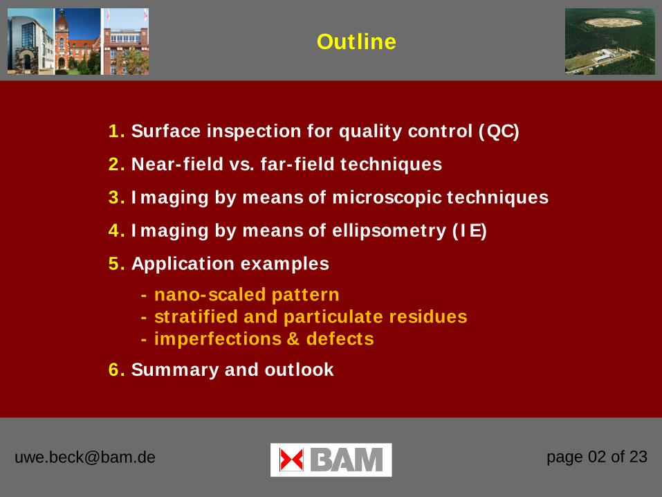
1. Surface inspection for quality control (QC)
2. Near-field vs. far-field techniques
3. Imaging by means of microscopic techniques
4. Imaging by means of ellipsometry (IE)
5. Application examples
- nano-scaled pattern - stratified and particulate residues - imperfections & defects
6. Summary and outlook

Surface Inspection for QC
General Requirements
page 03 of 23
Key product functionalities on the surface on the µm- and nm-scale, mostly film-based Huge variety of applications, e.g. micro- and optoelectronics, micro-devices, smart windows, sensor-on-chip, lab-on-chip, precision & ophthalmic optics, …
QC-1: material quality & chemical purity – qualitatively (validated fingerprints) QC-2: structural dimensions, film thickness – quantitatively (within specification) QC-3: applicable both to R&D and QC
QC-4: non-destructive, non-invasive QC-5: high lateral and vertical resolution, high depth of field QC-6: high sensitivity and material contrast to contaminations & defects
QC-7: ease of use, fast, atmospheric pressure QC-8: in-line, at-line, in-situ, on-line, i.e. technical far-field QC-9: robustness, reproducibility, maintenance-free

Metrology demands - field of inspection (FOI) cm2 to m2 - field of view (FOV) µm2 to cm2
- field of analysis (FOA) µm2 to cm2
- region of interest (ROI) ≤ µm2 to mm2
Evaluation demands - „all-in-one“ QC tool - materials - chemistry - dimensions (x, y, z) - thickness h LED light chip (36 x 36)mm2 Low-E glazing (3.21 x 6.00)m2
Source: OSRAM Source: VON ARDENNE
Surface Inspection for QC
Metrology & Evaluation Demands
page 04 of 23
Near-field vs. Far-field Techniques
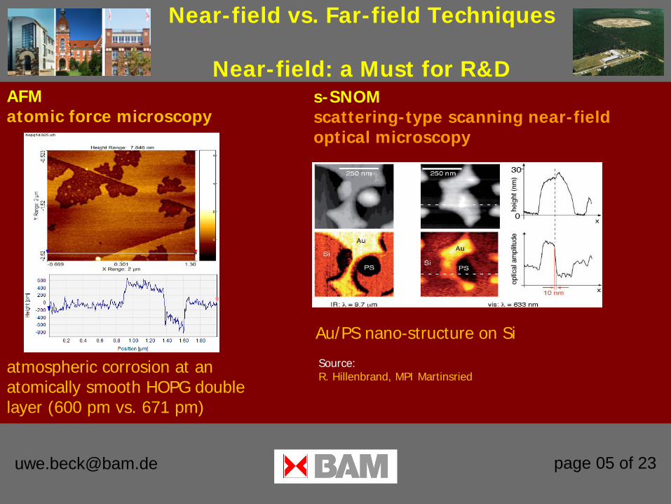
Near-field: a Must for R&D
page 05 of 23
Source: R. Hillenbrand, MPI Martinsried
s-SNOM scattering-type scanning near-field optical microscopy
atmospheric corrosion at an atomically smooth HOPG double layer (600 pm vs. 671 pm)
AFM atomic force microscopy
Au/PS nano-structure on Si

Near-field vs. Far-field Techniques
Far-field: a Must for QC
page 06 of 23
Conventional microscopic techniques normal incidence, i.e. p- and s-polarization undistinguishable
FM fluorescence microscopy LM light microscopy SM stereo microscopy IR-M IR-microscopy
diffraction limit: 0.5µm/10µm FWHMxy = 0.4λ /(n × sinα) FWHMz = 0.45λ /(1 - cosα) × n Advanced microscopic techniques normal incidence, i.e. p- and s-polarization undistinguishable, but with z-quantification CLSM confocal laser scanning microscopy WLIM white light interference microscopy diffraction limit: 0.5µm
FM: visible, not measurable
LM-DF: visible, not measurable

Microscopic Techniques
Light-, Stereo-, Fluorescence-, IR- Microscopy (LM, SM, FM, IR-M)
page 07 of 23
LM: microstructure of AlSi10Mg FM: PDA-Rhodamin/PS on SiO2
SM: glass fibre mat IR-M: adhesive failure
LM: rolling texture of steel
LM: electroplated Zn

Microscopic Techniques
WLIM & CLSM
page 08 of 23
1.14µm, 2.15µm, 5.17µm, 10.2µm monodisperse MF-beads
laser ripples on 100Cr6 laser crater in glass fibre single laser shot in ABS
WLIM broad R acceptance range ∆z, ∆x, ∆y Ra , Sa, …
CLSM R & T ∆z, ∆x, ∆y

State-of-the-art in
Microscopy
page 09 of 23
Source: St. Hell, Biophysical Journal, Vol. 105, issue 1, 07/2013, L01-L03
Microscopy (FM, …, CLSM) not an „all-in-one“ QC tool - measurement of dimensions
(x, y, z) but - no identificaction of materials - no verification of chemistry
(except for IR-M) - no direct determination of thicknesses hi
for QC
physical far-field (µm-range) vs. technical far-field (dm-range)
STED stimulated emission depletion, normal incidence below diffraction limit down to 10 nm, fluorescence required
BAM Brewster angle microscopy, at oblique incidence, with monolayer sensitivity, Rp polarisation matters
monopalmitoyl-rac-Glycerol air/water interface Source: Accurion GmbH, Göttingen
protein complex (FHWM 14 nm)

Brewster-angle Microscopy
vs. Imaging Ellipsometry at/near Brewster Angle
[email protected] page 10 of 23
From optically thin to thick medium: Brewster angle has to be considered

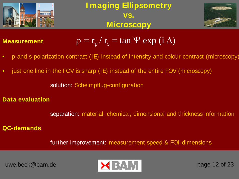
Imaging Ellipsometry
vs. Microscopy
page 11 of 23
oblique incidence: p- & s-amplitudes ( Ψ ) and phase (Δ ) matter at/near Brewster angle: i.e. tan ϑB = n and for incidenting p-polarized light, there is no reflected intensity, i.e. the (known) substrate „vanishes“ in reflection high surface sensitivity (to unknown contaminations) settings to adjust: PCA-configuration, AOI (ϑ) vs. wavelength λ vs. n(λ), light source three images (video, Ψ , Δ ) with material, chemical, dimensional and thickness information video-image (R ), Ψ -image (|𝒓𝒑/𝒓𝒔|), Δ -image (φp - φs)
Imaging Ellipsometry
vs. Microscopy
page 12 of 23
Measurement ρ = rp / rs = tan Ψ exp (i ∆) • p-and s-polarization contrast (IE) instead of intensity and colour contrast (microscopy) • just one line in the FOV is sharp (IE) instead of the entire FOV (microscopy) solution: Scheimpflug-configuration Data evaluation separation: material, chemical, dimensional and thickness information QC-demands further improvement: measurement speed & FOI-dimensions

Imaging Ellipsometry
Scheimpflug Configuration
page 13 of 23
Dual head gonio-spectros- copic imaging ellipsometer (IE & AFM) EP3@BAM automated variable angle, flow cell, SPR kit
Scheimpflug configuration, sharp image over entire FOV with ultra-objective: EP3-ultra@BAM EP4@Accurion
Application Example 1
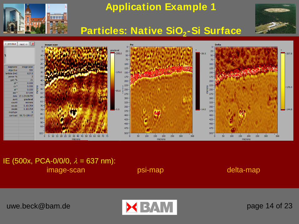
Particles: Native SiO2-Si Surface
page 14 of 23
IE (500x, PCA-0/0/0, λ = 637 nm): image-scan psi-map delta-map

Application Example 2
Fingerprint: Native SiO2-Si Surface
page 15 of 23
IE (500x, PCA-0/0/0, image-scan): Xe-lamp 560 nm laser 637 nm

Application Example 3
Dried Stain: Native SiO2-Si Surface
page 16 of 20
IE: image-scan (500x, PCA-0/0/0, image-scan): Xe-lamp 560 nm laser 637 nm
IE: delta-map (500x, PCA: 45/35/25-Xe, 35/25/15-laser) Xe-lamp 560 nm laser 637 nm

Application Example 4
0.5nm Film Pattern: AFM vs. IE
page 17 of 23
AFM: FOV (2 x 2)µm2
IE: image-scan & delta-map FOV (1200 x 1800)µm2
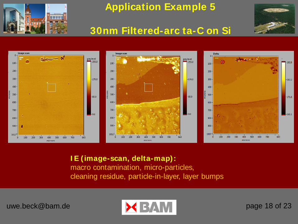
Application Example 5
30nm Filtered-arc ta-C on Si
page 18 of 23
IE (image-scan, delta-map): macro contamination, micro-particles, cleaning residue, particle-in-layer, layer bumps

Application Example 6
Hidden Forensic In-layer Features
page 19 of 23
LM-DIC polarized light, special illumination almost invisible using LM, …,WLIM
IE (delta-map) phase-contrast imaging depolarisation-contrast imaging

Application Example 7
Micro-patterned Glass Surfaces
page 20 of 23
IE: image-scan residue from chemical etching
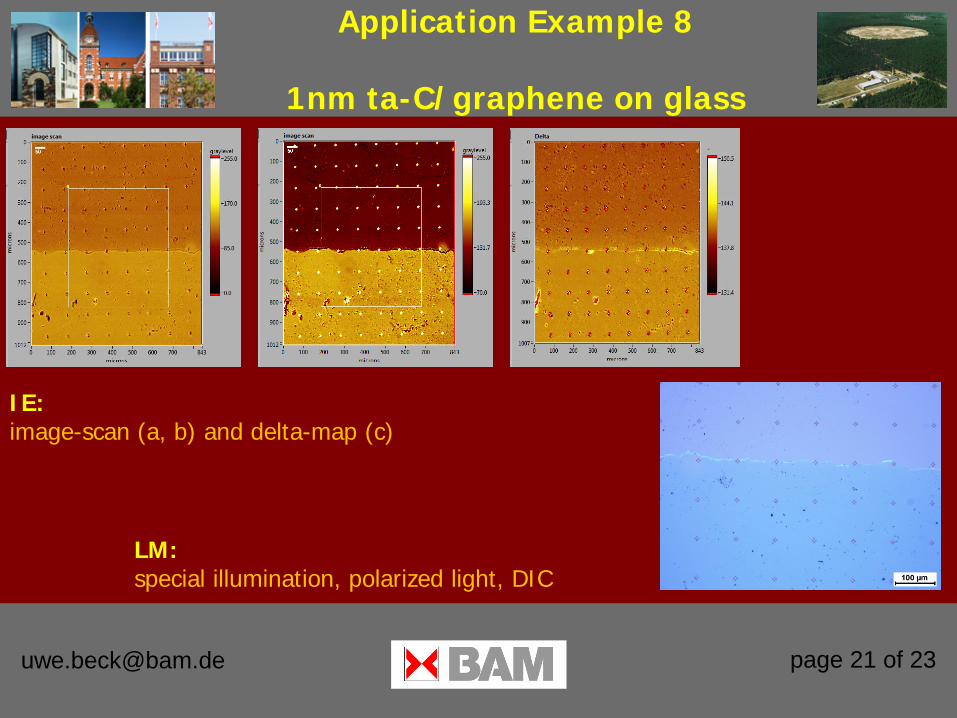
Application Example 8
1nm ta-C/graphene on glass
page 21 of 23
IE: image-scan (a, b) and delta-map (c)
LM: special illumination, polarized light, DIC

Summary & Outlook
page 22 of 23
Imaging ellipsometry vs. microscpoy materials (n, k, ε1, ε2) chemistry (residue from cleaning, dried stain, fingerprint-contamination) dimensions (micro-pattern: structured films and wet etching in glass; particles; preparation artefacts) thickness (0.5nm island film, 1nm ta-C/graphene, 30nm ta-C) Mapping & imaging: image-scan, psi- and delta-maps; ROI: 10µm2 to 2mm2 Scheimpflug-objective a further step to QC-applications Faster search for best contrast, larger areas, further improvement of measurement speed, and SOP-adaptation to selected industrial applications will be addressed in a new project.

Thanks for your Attendence and Attention
Upcoming events: ICSE-7, Berlin, Germany, 2016 Organized by: ISAS: N. Esser, K. Hinrichs & BAM: U. Beck, A. Hertwig
page 23 of 23
division 6.7, branch FB: 12203 Berlin, Unter den Eichen 44-46