Embed Size (px)
Citation preview

7 Series FPGAs SelectIO Resources
User Guide
UG471 (v1.9) August 22, 2017

7 Series FPGAs SelectIO Resources User Guide www.xilinx.com UG471 (v1.9) August 22, 2017
The information disclosed to you hereunder (the "Materials") is provided solely for the selection and use of Xilinx products. To the maximum extent permitted by applicable law: (1) Materials are made available "AS IS" and with all faults, Xilinx hereby DISCLAIMS ALL WARRANTIES AND CONDITIONS, EXPRESS, IMPLIED, OR STATUTORY, INCLUDING BUT NOT LIMITED TO WARRANTIES OF MERCHANTABILITY, NON-INFRINGEMENT, OR FITNESS FOR ANY PARTICULAR PURPOSE; and (2) Xilinx shall not be liable (whether in contract or tort, including negligence, or under any other theory of liability) for any loss or damage of any kind or nature related to, arising under, or in connection with, the Materials (including your use of the Materials), including for any direct, indirect, special, incidental, or consequential loss or damage (including loss of data, profits, goodwill, or any type of loss or damage suffered as a result of any action brought by a third party) even if such damage or loss was reasonably foreseeable or Xilinx had been advised of the possibility of the same. Xilinx assumes no obligation to correct any errors contained in the Materials, or to advise you of any corrections or update. You may not reproduce, modify, distribute, or publicly display the Materials without prior written consent. Certain products are subject to the terms and conditions of the Limited Warranties which can be viewed at http://www.xilinx.com/warranty.htm; IP cores may be subject to warranty and support terms contained in a license issued to you by Xilinx. Xilinx products are not designed or intended to be fail-safe or for use in any application requiring fail-safe performance; you assume sole risk and liability for use of Xilinx products in Critical Applications: http://www.xilinx.com/warranty.htm#critapps.
AUTOMOTIVE APPLICATIONS DISCLAIMERAUTOMOTIVE PRODUCTS (IDENTIFIED AS “XA” IN THE PART NUMBER) ARE NOT WARRANTED FOR USE IN THE DEPLOYMENT OF AIRBAGS OR FOR USE IN APPLICATIONS THAT AFFECT CONTROL OF A VEHICLE (“SAFETY APPLICATION”) UNLESS THERE IS A SAFETY CONCEPT OR REDUNDANCY FEATURE CONSISTENT WITH THE ISO 26262 AUTOMOTIVE SAFETY STANDARD (“SAFETY DESIGN”). CUSTOMER SHALL, PRIOR TO USING OR DISTRIBUTING ANY SYSTEMS THAT INCORPORATE PRODUCTS, THOROUGHLY TEST SUCH SYSTEMS FOR SAFETY PURPOSES. USE OF PRODUCTS IN A SAFETY APPLICATION WITHOUT A SAFETY DESIGN IS FULLY AT THE RISK OF CUSTOMER, SUBJECT ONLY TO APPLICABLE LAWS AND REGULATIONS GOVERNING LIMITATIONS ON PRODUCT LIABILITY.
© Copyright 2011–2017 Xilinx, Inc. XILINX, the Xilinx logo, Virtex, Zynq, Artix, Kintex, Spartan, ISE and other designated brands included herein are trademarks of Xilinx in the United States and other countries. All other trademarks are the property of their respective owners.
Revision HistoryThe following table shows the revision history for this document.
Date Version Revision
03/01/2011 1.0 Initial Xilinx release.
04/06/2011 1.0.1 Updated disclaimer and copyright sections on page 2.
05/31/2011 1.1 Added New Features. Updated the example device including Figure 1-15 and the partgen example on page 24. Added VRN/VRP External Resistance Design Migration Guidelines.
Updated the BITSLIP Submodule section including Figure 3-12. Removed Figure 3-13: Bits from Data Input Stream (D) of Figure 3-12.
07/20/2012 1.2 Updated paragraph before Table 1-1. Added LVDS signaling to Table 1-1. Updated VCCO and VCCAUX_IO. Updated Xilinx DCI. Removed VCCINT. Added Match_cycle Configuration Option, DCIUpdateMode Configuration Option, DCIRESET Primitive, and Special DCI Requirements for Some Banks. Updated DCI Cascading. Updated DCI cascading guidelines after Figure 1-7. Updated table note in Table 1-3. Added Uncalibrated Split Termination in High-Range I/O Banks (IN_TERM). Updated 7 Series FPGA SelectIO Primitives. Added DCI_CASCADE Constraint and VCCAUX_IO Constraint. Updated IBUF_LOW_PWR Attribute, Output Slew Rate Attributes, Output Drive Strength Attributes, PULLUP/PULLDOWN/KEEPER Attribute for IBUF, OBUFT, and IOBUF, and 7 Series FPGA I/O Resource VHDL/Verilog Examples. Put Internal VREF inside Differential Termination Attribute, page 49. Updated DRIVE attribute in Table 1-10. Updated titles of Figure 1-41 through Figure 1-44. Updated LVDS and LVDS_25 (Low Voltage Differential Signaling), including adding Figure 1-72. Added IN_TERM attribute to SSTL (Stub-Series Terminated Logic). Added table note to Table 1-55. Added Simultaneous Switching Outputs.

UG471 (v1.9) August 22, 2017 www.xilinx.com 7 Series FPGAs SelectIO Resources User Guide
07/20/2012 1.2(Cont’d)
Updated ILOGIC Resources. In Table 2-3, added TICOCKD/TIOCKDD and removed TICE1Q. Updated Input Delay Resources (IDELAY). Updated functional description of LD port in Table 2-4. In IDELAY Ports, updated Module Load - LD and Increment/Decrement Signals - CE, INC, and added Pipeline Register Load - LDPIPEEN and Pipeline Register Reset - REGRST. Removed Table 2-5: “Control Pin Descriptions.” Updated descriptions of IDELAY_TYPE and IDELAY_VALUE in Table 2-5. Updated IDELAY_TYPE Attribute, IDELAY_VALUE Attribute, and HIGH_PERFORMANCE_MODE Attribute. Updated IDELAY Timing. Updated text before Figure 2-12. Updated Stability after an Increment/Decrement Operation. Updated IDELAYCTRL, including Figure 2-16. Added paragraph about OLOGICE2 and OLOGICE3 to OLOGIC Resources. Updated first paragraph of Output Delay Resources (ODELAY)—Not Available in HR Banks. Updated functions of REGRST, LD, CNTVALUEIN, LDPIPEEN, and CNTVALUEOUT in Table 2-13. Added description of VAR_LOAD_PIPE mode to Module Load - LD. Added Pipeline Register Load - LDPIPEEN and Pipeline Register Reset - REGRST. Updated Count Value In - CNTVALUEIN, Count Value Out - CNTVALUEOUT, and Increment/Decrement Signals - CE, INC. Removed Table 2-14: “Control Pin Descriptions.” Updated descriptions of ODELAY_TYPE and ODELAY_VALUE in Table 2-14. Updated ODELAY Attributes. Added ODELAY Modes. Updated text before Figure 2-26.
Updated Reset Input - RST, page 149. Added INIT_Q and SRVAL_Q attributes to Table 3-2. Updated bulleted list after Figure 3-6 and in MEMORY Interface Type. Updated Figure 3-7. Updated ISERDESE2 Width Expansion, BITSLIP Submodule, and Data Parallel-to-Serial Converter. Deleted the OCBEXTEND pin in Figure 3-14. Updated descriptions of OFB and TFB in Table 3-6. Updated Output Feedback from OSERDESE2 - OFB, 3-state Control Output - TFB, and Reset Input - RST, page 164. Updated OSERDESE2 Clocking Methods and OSERDESE2 Width Expansion. Updated latencies in Table 3-11. Added IO_FIFO Overview. Updated Resetting the IO_FIFO.
Added Appendix A, Termination Options for SSO Noise Analysis.
10/31/2012 1.3 Removed XC7V1500T from third bullet after Figure 1-7.
05/13/2014 1.4 Updated VCCO. Added item to bulleted list after Figure 1-7. Updated paragraph after Figure 1-10. In VRN/VRP External Resistance Design Migration Guidelines, updated first two paragraphs and added description of power rating. Updated title of Figure 1-11 and Figure 1-12. Updated step 4 of DCI in 7 Series FPGAs I/O Standards. Updated Figure 1-14. Updated first paragraph of Uncalibrated Split Termination in High-Range I/O Banks (IN_TERM). Added IOBUF_DCIEN, IOBUF_INTERMDISABLE, IOBUFDS_DIFF_OUT_DCIEN, IOBUFDS_DIFF_OUT_INTERMDISABLE, and IOBUFDS_INTERMDISABLE to 7 Series FPGA SelectIO Primitives. Removed O output from Figure 1-22 and following description. Updated HSTL_ II_T_DCI and HSTL_ II_T_DCI_18. Added IBUFDS_DIFF_OUT_INTERMDISABLE, IOBUF_DCIEN, and IOBUF_INTERMDISABLE. Updated connections in Figure 1-28, Figure 1-30, Figure 1-31, and Figure 1-32. Reversed RVRN and RVRP in Figure 1-46, Figure 1-48, Figure 1-49, Figure 1-50, Figure 1-52, Figure 1-54, Figure 1-55, Figure 1-56, Figure 1-57, Figure 1-58, Figure 1-60, Figure 1-62, and Figure 1-63. Added note to SSTL18_II, SSTL15, SSTL135, DIFF_SSTL18_II, DIFF_SSTL15, DIFF_SSTL135. Updated fifth paragraph of SSTL (Stub-Series Terminated Logic). Removed Thevenin equivalent of R/2 and description of source termination series resistors from SSTL18_I_DCI, DIFF_SSTL18_I_DCI, SSTL18_II, SSTL15, SSTL135, DIFF_SSTL18_II, DIFF_SSTL15, DIFF_SSTL135, SSTL18_II_DCI, SSTL_15_DCI, SSTL135_DCI, DIFF_SSTL18_II_DCI, DIFF_SSTL_15_DCI, DIFF_ SSTL135_DCI, SSTL18_II_T_DCI, SSTL15_T_DCI, SSTL135_T_DCI, DIFF_SSTL18_II_T_DCI, DIFF_SSTL15_T_DCI, DIFF_ SSTL135_T_DCI, and SSTL12, SSTL12_DCI, SSTL12_T_DCI, DIFF_SSTL12, DIFF_SSTL12_DCI, DIFF_SSTL12_T_DCI. Updated Figure 1-57 and Figure 1-59.
Date Version Revision

7 Series FPGAs SelectIO Resources User Guide www.xilinx.com UG471 (v1.9) August 22, 2017
05/13/2014 1.4(Cont’d)
Added to list of criteria after Table 1-44. Added note to Table 1-48. Updated description after Table 1-51. Updated VCCO Input column in Table 1-55. Added note 3 to Table 1-56.
Updated DLYIN connection in Figure 2-4. Updated Clock Input - C, page 117. Updated description of PIPE_SEL in Table 2-5 and Table 2-14. Added VAR_LOAD description to first paragraph of Stability after an Increment/Decrement Operation, page 123. Removed center I/Os from Figure 2-16. Updated Data Output - DATAOUT, page 135. In ODELAY Modes, replaced ODELAYCTRL with IDELAYCTRL.
In Table 3-1, added CLKDIVP and updated descriptions of OCLK and OCLKB. Updated High-Speed Clock for Strobe-Based Memory Interfaces and Oversampling Mode - OCLK and Reset Input - RST. Added IOBDELAY to Table 3-2. Updated bullets in MEMORY Interface Type. Updated bullets in OVERSAMPLE Interface Type. Updated Figure 3-7. Added sentence about ISERDESE2 being reset to Guidelines for Using the Bitslip Submodule. Removed Bitslip submodule from description of CLKDIV in Table 3-6. Added TBYTE_CTL and TBYTE_SRC to Table 3-7. In Figure 3-18, shifted OQ, TQ, and OBUFT.O by one CLK edge.
05/15/2015 1.5 Added paragraph about overvoltage protection mode to VCCO. Added State of I/Os During and After Configuration. Updated Special DCI Requirements for Some Banks. In IOSTANDARD Attribute, replaced DIFF_HSTL18_II with DIFF_HSTL_II_18. Reversed RVRN and RVRP resistors in left side IOB of DCI terminations in Figure 1-49, Figure 1-50, Figure 1-52, Figure 1-54, Figure 1-57, Figure 1-58, Figure 1-60, and Figure 1-62. Added note 2 to Table 1-55. Added Vivado Design Suite to Pin Planning to Mitigate SSO Sensitivity.
Updated description of clock input C in IDELAY Ports and ODELAY Ports. Replaced SR with S/R in Figure 2-17, Figure 2-20, and Table 2-10.
09/18/2015 1.6 Replaced SR with S/R throughout. Added note about set and reset pins to Table 2-1 and Table 2-10. In RDY - Ready, updated sentence about RDY signal being deasserted if REFCLK is held High or Low for more than one clock period.
In Table 3-6, changed TBYTEOUT port type from input to output.
09/15/2016 1.7 Updated first paragraph of VCCO. Added reference to UG912: Vivado Design Suite Properties Reference Guide in Uncalibrated Split Termination in High-Range I/O Banks (IN_TERM) and 7 Series FPGA SelectIO Attributes/Constraints. Added description of termination for unused I/Os to PULLUP/PULLDOWN/KEEPER Attribute for IBUF, OBUFT, and IOBUF.
Updated third bullet in OSERDESE2 Clocking Methods. In Table 3-11, updated DDR 14:1 latency to 5 CLK cycles.
09/27/2016 1.8 Added Spartan-7 family to Preface. Updated Reset Input - RST. Removed bullet describing CLK driven by BUFG and CLKDIV driven by a different BUFG from NETWORKING Interface Type and OSERDESE2 Clocking Methods.
08/22/2017 1.9 Replaced HR with HP in second paragraph of VCCO. Expanded description of ZHOLD in ILOGIC Resources. Updated REFCLK_FREQUENCY value and description in Table 2-5 and Table 2-14. Updated description of Clock Input from Clock Buffer - CLKIN.
Updated descriptions of SHIFTOUT1, SHIFTOUT2, SHIFTIN1, and SHIFTIN2 in Table 3-6. Updated input span to D1–D8 in Timing Characteristics of 8:1 DDR Serialization.
Date Version Revision

7 Series FPGAs SelectIO Resources User Guide www.xilinx.com 5UG471 (v1.9) August 22, 2017
Revision History . . . . . . . . . . . . . . . . . . . . . . . . . . . . . . . . . . . . . . . . . . . . . . . . . . . . . . . . . . . . . 2
Preface: About This GuideGuide Contents . . . . . . . . . . . . . . . . . . . . . . . . . . . . . . . . . . . . . . . . . . . . . . . . . . . . . . . . . . . . . 11Additional Resources . . . . . . . . . . . . . . . . . . . . . . . . . . . . . . . . . . . . . . . . . . . . . . . . . . . . . . . 11
Chapter 1: SelectIO ResourcesI/O Tile Overview . . . . . . . . . . . . . . . . . . . . . . . . . . . . . . . . . . . . . . . . . . . . . . . . . . . . . . . . . . . 13New Features . . . . . . . . . . . . . . . . . . . . . . . . . . . . . . . . . . . . . . . . . . . . . . . . . . . . . . . . . . . . . . . 14SelectIO Resources Introduction . . . . . . . . . . . . . . . . . . . . . . . . . . . . . . . . . . . . . . . . . . . . 15SelectIO Resources General Guidelines . . . . . . . . . . . . . . . . . . . . . . . . . . . . . . . . . . . . . 17
7 Series FPGA I/O Bank Rules . . . . . . . . . . . . . . . . . . . . . . . . . . . . . . . . . . . . . . . . . . . . . . 17Supply Voltages for the SelectIO Pins. . . . . . . . . . . . . . . . . . . . . . . . . . . . . . . . . . . . . . . 18State of I/Os During and After Configuration . . . . . . . . . . . . . . . . . . . . . . . . . . . . . . . . 19
7 Series FPGA DCI—Only available in the HP I/O banks . . . . . . . . . . . . . . . . . . . . 19Introduction . . . . . . . . . . . . . . . . . . . . . . . . . . . . . . . . . . . . . . . . . . . . . . . . . . . . . . . . . . . . . 19Xilinx DCI . . . . . . . . . . . . . . . . . . . . . . . . . . . . . . . . . . . . . . . . . . . . . . . . . . . . . . . . . . . . . . . 20Match_cycle Configuration Option . . . . . . . . . . . . . . . . . . . . . . . . . . . . . . . . . . . . . . . . . . 21DCIUpdateMode Configuration Option . . . . . . . . . . . . . . . . . . . . . . . . . . . . . . . . . . . . . 21DCIRESET Primitive . . . . . . . . . . . . . . . . . . . . . . . . . . . . . . . . . . . . . . . . . . . . . . . . . . . . . . 22Special DCI Requirements for Some Banks . . . . . . . . . . . . . . . . . . . . . . . . . . . . . . . . . . . 22DCI Cascading . . . . . . . . . . . . . . . . . . . . . . . . . . . . . . . . . . . . . . . . . . . . . . . . . . . . . . . . . . . 22Controlled Impedance Driver (Source Termination) . . . . . . . . . . . . . . . . . . . . . . . . . . . 25Controlled Impedance Driver with Half Impedance (Source Termination) . . . . . . . . 25Split-Termination DCI (Thevenin Equivalent Termination to VCCO/2) . . . . . . . . . . 26VRN/VRP External Resistance Design Migration Guidelines . . . . . . . . . . . . . . . . . . . 27DCI and 3-state DCI (T_DCI) . . . . . . . . . . . . . . . . . . . . . . . . . . . . . . . . . . . . . . . . . . . . . . . 28DCI in 7 Series FPGAs I/O Standards . . . . . . . . . . . . . . . . . . . . . . . . . . . . . . . . . . . . . . . 29DCI Usage Examples . . . . . . . . . . . . . . . . . . . . . . . . . . . . . . . . . . . . . . . . . . . . . . . . . . . . . . 31
Uncalibrated Split Termination in High-Range I/O Banks (IN_TERM) . . . . . . . 337 Series FPGA SelectIO Primitives. . . . . . . . . . . . . . . . . . . . . . . . . . . . . . . . . . . . . . . . . . . 34
IBUF and IBUFG . . . . . . . . . . . . . . . . . . . . . . . . . . . . . . . . . . . . . . . . . . . . . . . . . . . . . . . . . 35IBUF_IBUFDISABLE . . . . . . . . . . . . . . . . . . . . . . . . . . . . . . . . . . . . . . . . . . . . . . . . . . . . . . 35IBUF_INTERMDISABLE . . . . . . . . . . . . . . . . . . . . . . . . . . . . . . . . . . . . . . . . . . . . . . . . . . 36IBUFDS and IBUFGDS . . . . . . . . . . . . . . . . . . . . . . . . . . . . . . . . . . . . . . . . . . . . . . . . . . . . 36IBUFDS_DIFF_OUT and IBUFGDS_DIFF_OUT . . . . . . . . . . . . . . . . . . . . . . . . . . . . . . . 37IBUFDS_DIFF_OUT_IBUFDISABLE . . . . . . . . . . . . . . . . . . . . . . . . . . . . . . . . . . . . . . . . 37IBUFDS_IBUFDISABLE . . . . . . . . . . . . . . . . . . . . . . . . . . . . . . . . . . . . . . . . . . . . . . . . . . . 37IBUFDS_INTERMDISABLE . . . . . . . . . . . . . . . . . . . . . . . . . . . . . . . . . . . . . . . . . . . . . . . . 38IBUFDS_DIFF_OUT_INTERMDISABLE . . . . . . . . . . . . . . . . . . . . . . . . . . . . . . . . . . . . . 38IOBUF . . . . . . . . . . . . . . . . . . . . . . . . . . . . . . . . . . . . . . . . . . . . . . . . . . . . . . . . . . . . . . . . . . 39IOBUF_DCIEN . . . . . . . . . . . . . . . . . . . . . . . . . . . . . . . . . . . . . . . . . . . . . . . . . . . . . . . . . . . 39IOBUF_INTERMDISABLE . . . . . . . . . . . . . . . . . . . . . . . . . . . . . . . . . . . . . . . . . . . . . . . . . 40IOBUFDS . . . . . . . . . . . . . . . . . . . . . . . . . . . . . . . . . . . . . . . . . . . . . . . . . . . . . . . . . . . . . . . . 41IOBUFDS_DCIEN . . . . . . . . . . . . . . . . . . . . . . . . . . . . . . . . . . . . . . . . . . . . . . . . . . . . . . . . 41
Table of Contents
Send Feedback

6 www.xilinx.com 7 Series FPGAs SelectIO Resources User GuideUG471 (v1.9) August 22, 2017
IOBUFDS_DIFF_OUT . . . . . . . . . . . . . . . . . . . . . . . . . . . . . . . . . . . . . . . . . . . . . . . . . . . . . 42IOBUFDS_DIFF_OUT_DCIEN . . . . . . . . . . . . . . . . . . . . . . . . . . . . . . . . . . . . . . . . . . . . . 43IOBUFDS_DIFF_OUT_INTERMDISABLE . . . . . . . . . . . . . . . . . . . . . . . . . . . . . . . . . . . 44IOBUFDS_INTERMDISABLE . . . . . . . . . . . . . . . . . . . . . . . . . . . . . . . . . . . . . . . . . . . . . . 44OBUF . . . . . . . . . . . . . . . . . . . . . . . . . . . . . . . . . . . . . . . . . . . . . . . . . . . . . . . . . . . . . . . . . . . 45OBUFDS . . . . . . . . . . . . . . . . . . . . . . . . . . . . . . . . . . . . . . . . . . . . . . . . . . . . . . . . . . . . . . . . 45OBUFT . . . . . . . . . . . . . . . . . . . . . . . . . . . . . . . . . . . . . . . . . . . . . . . . . . . . . . . . . . . . . . . . . . 46OBUFTDS . . . . . . . . . . . . . . . . . . . . . . . . . . . . . . . . . . . . . . . . . . . . . . . . . . . . . . . . . . . . . . . 46
7 Series FPGA SelectIO Attributes/Constraints . . . . . . . . . . . . . . . . . . . . . . . . . . . . . . 46DCI_CASCADE Constraint . . . . . . . . . . . . . . . . . . . . . . . . . . . . . . . . . . . . . . . . . . . . . . . . 46Location Constraints . . . . . . . . . . . . . . . . . . . . . . . . . . . . . . . . . . . . . . . . . . . . . . . . . . . . . . 47IOSTANDARD Attribute . . . . . . . . . . . . . . . . . . . . . . . . . . . . . . . . . . . . . . . . . . . . . . . . . . 47IBUF_LOW_PWR Attribute . . . . . . . . . . . . . . . . . . . . . . . . . . . . . . . . . . . . . . . . . . . . . . . . 47Output Slew Rate Attributes . . . . . . . . . . . . . . . . . . . . . . . . . . . . . . . . . . . . . . . . . . . . . . . 48Output Drive Strength Attributes . . . . . . . . . . . . . . . . . . . . . . . . . . . . . . . . . . . . . . . . . . . 48PULLUP/PULLDOWN/KEEPER Attribute for IBUF, OBUFT, and IOBUF . . . . . . . 49Differential Termination Attribute . . . . . . . . . . . . . . . . . . . . . . . . . . . . . . . . . . . . . . . . . . 49
Internal VREF. . . . . . . . . . . . . . . . . . . . . . . . . . . . . . . . . . . . . . . . . . . . . . . . . . . . . . . . . . 50VCCAUX_IO Constraint . . . . . . . . . . . . . . . . . . . . . . . . . . . . . . . . . . . . . . . . . . . . . . . . . . . 507 Series FPGA I/O Resource VHDL/Verilog Examples . . . . . . . . . . . . . . . . . . . . . . . . 51
Supported I/O Standards and Terminations . . . . . . . . . . . . . . . . . . . . . . . . . . . . . . . . . 51LVTTL (Low Voltage TTL) . . . . . . . . . . . . . . . . . . . . . . . . . . . . . . . . . . . . . . . . . . . . . . . . . 51LVCMOS (Low Voltage CMOS) . . . . . . . . . . . . . . . . . . . . . . . . . . . . . . . . . . . . . . . . . . . . 54
LVDCI (Low-Voltage Digitally Controlled Impedance) . . . . . . . . . . . . . . . . . . . . . . . . . 56LVDCI_DV2 . . . . . . . . . . . . . . . . . . . . . . . . . . . . . . . . . . . . . . . . . . . . . . . . . . . . . . . . . . 57HSLVDCI (High-Speed LVDCI) . . . . . . . . . . . . . . . . . . . . . . . . . . . . . . . . . . . . . . . . . . . 59
HSTL (High-Speed Transceiver Logic) . . . . . . . . . . . . . . . . . . . . . . . . . . . . . . . . . . . . . . . 60HSTL_ I and HSTL_ I_18 . . . . . . . . . . . . . . . . . . . . . . . . . . . . . . . . . . . . . . . . . . . . . . . . 60HSTL_I_12 . . . . . . . . . . . . . . . . . . . . . . . . . . . . . . . . . . . . . . . . . . . . . . . . . . . . . . . . . . . 60HSTL_ I_DCI and HSTL_ I_DCI_18 . . . . . . . . . . . . . . . . . . . . . . . . . . . . . . . . . . . . . . . . 60HSTL_ II and HSTL_ II_18 . . . . . . . . . . . . . . . . . . . . . . . . . . . . . . . . . . . . . . . . . . . . . . . 60HSTL_ II_DCI and HSTL_ II_DCI_18 . . . . . . . . . . . . . . . . . . . . . . . . . . . . . . . . . . . . . . . 61HSTL_ II_T_DCI and HSTL_ II_T_DCI_18 . . . . . . . . . . . . . . . . . . . . . . . . . . . . . . . . . . . 61DIFF_HSTL_I and DIFF_HSTL_I_18. . . . . . . . . . . . . . . . . . . . . . . . . . . . . . . . . . . . . . . . 61DIFF_HSTL_I_DCI and DIFF_HSTL_I_DCI_18 . . . . . . . . . . . . . . . . . . . . . . . . . . . . . . . 61DIFF_HSTL_ II and DIFF_HSTL_II_18 . . . . . . . . . . . . . . . . . . . . . . . . . . . . . . . . . . . . . . 61DIFF_HSTL_II_DCI and DIFF_HSTL_II_DCI_18 . . . . . . . . . . . . . . . . . . . . . . . . . . . . . . 62DIFF_HSTL_II_T_DCI and DIFF_HSTL_II_T_DCI_18 . . . . . . . . . . . . . . . . . . . . . . . . . . 62
HSTL Class I (1.2V, 1.5V, or 1.8V) . . . . . . . . . . . . . . . . . . . . . . . . . . . . . . . . . . . . . . . . . . . 62Differential HSTL Class I . . . . . . . . . . . . . . . . . . . . . . . . . . . . . . . . . . . . . . . . . . . . . . . . . . 64HSTL Class II . . . . . . . . . . . . . . . . . . . . . . . . . . . . . . . . . . . . . . . . . . . . . . . . . . . . . . . . . . . . 66Differential HSTL Class II . . . . . . . . . . . . . . . . . . . . . . . . . . . . . . . . . . . . . . . . . . . . . . . . . . 68HSTL_II_T_DCI (1.5V or 1.8V) Split-Thevenin Termination (3-state) . . . . . . . . . . . . . 72SSTL (Stub-Series Terminated Logic) . . . . . . . . . . . . . . . . . . . . . . . . . . . . . . . . . . . . . . . . 74
SSTL15_R, SSTL135_R, DIFF_SSTL15_R, DIFF_SSTL135_R . . . . . . . . . . . . . . . . . . . . . . 76SSTL18_I, DIFF_SSTL18_I . . . . . . . . . . . . . . . . . . . . . . . . . . . . . . . . . . . . . . . . . . . . . . . . 76SSTL18_I_DCI, DIFF_SSTL18_I_DCI . . . . . . . . . . . . . . . . . . . . . . . . . . . . . . . . . . . . . . . 76SSTL18_II, SSTL15, SSTL135, DIFF_SSTL18_II, DIFF_SSTL15, DIFF_SSTL135 . . . . . . . . 76SSTL18_II_DCI, SSTL_15_DCI, SSTL135_DCI, DIFF_SSTL18_II_DCI, DIFF_SSTL_15_DCI, DIFF_
SSTL135_DCI . . . . . . . . . . . . . . . . . . . . . . . . . . . . . . . . . . . . . . . . . . . . . . . . . . . . . . . 77SSTL18_II_T_DCI, SSTL15_T_DCI, SSTL135_T_DCI, DIFF_SSTL18_II_T_DCI,
DIFF_SSTL15_T_DCI, DIFF_ SSTL135_T_DCI . . . . . . . . . . . . . . . . . . . . . . . . . . . . . . 77SSTL12, SSTL12_DCI, SSTL12_T_DCI, DIFF_SSTL12, DIFF_SSTL12_DCI, DIFF_SSTL12_T_DCI77
Send Feedback

7 Series FPGAs SelectIO Resources User Guide www.xilinx.com 7UG471 (v1.9) August 22, 2017
SSTL18, SSTL15, SSTL135, SSTL12 . . . . . . . . . . . . . . . . . . . . . . . . . . . . . . . . . . . . . . . . . . 78Differential SSTL18, SSTL15, SSTL135, SSTL12 . . . . . . . . . . . . . . . . . . . . . . . . . . . . . . . . 80SSTL18, SSTL15, SSTL135, or SSTL12 (T_DCI) Termination . . . . . . . . . . . . . . . . . . . . . 84HSUL_12 (High Speed Unterminated Logic) . . . . . . . . . . . . . . . . . . . . . . . . . . . . . . . . . 84
HSUL_12 and DIFF_HSUL_12 . . . . . . . . . . . . . . . . . . . . . . . . . . . . . . . . . . . . . . . . . . . . 84HSUL_DCI_12 and DIFF_HSUL_12_DCI . . . . . . . . . . . . . . . . . . . . . . . . . . . . . . . . . . . . 85
HSUL_12 . . . . . . . . . . . . . . . . . . . . . . . . . . . . . . . . . . . . . . . . . . . . . . . . . . . . . . . . . . . . . . . . 85Differential HSUL_12 . . . . . . . . . . . . . . . . . . . . . . . . . . . . . . . . . . . . . . . . . . . . . . . . . . . . . 86MOBILE_DDR (Low Power DDR) . . . . . . . . . . . . . . . . . . . . . . . . . . . . . . . . . . . . . . . . . . 88Summary of Memory Interface IOSTANDARDs and Attributes Supported . . . . . . . 88LVDS and LVDS_25 (Low Voltage Differential Signaling) . . . . . . . . . . . . . . . . . . . . . . 91
Transmitter Termination. . . . . . . . . . . . . . . . . . . . . . . . . . . . . . . . . . . . . . . . . . . . . . . . . 91Receiver Termination . . . . . . . . . . . . . . . . . . . . . . . . . . . . . . . . . . . . . . . . . . . . . . . . . . . 91
RSDS (Reduced Swing Differential Signaling) . . . . . . . . . . . . . . . . . . . . . . . . . . . . . . . . 94Mini-LVDS (Mini Low Voltage Differential Signaling) . . . . . . . . . . . . . . . . . . . . . . . . . 94PPDS (Point-to-Point Differential Signaling) . . . . . . . . . . . . . . . . . . . . . . . . . . . . . . . . . . 95TMDS (Transition Minimized Differential Signaling) . . . . . . . . . . . . . . . . . . . . . . . . . . 95BLVDS (Bus LVDS) . . . . . . . . . . . . . . . . . . . . . . . . . . . . . . . . . . . . . . . . . . . . . . . . . . . . . . . 96
Rules for Combining I/O Standards in the Same Bank . . . . . . . . . . . . . . . . . . . . . . . 97Simultaneous Switching Outputs. . . . . . . . . . . . . . . . . . . . . . . . . . . . . . . . . . . . . . . . . . . 104
Pin Planning to Mitigate SSO Sensitivity . . . . . . . . . . . . . . . . . . . . . . . . . . . . . . . . . . . . 104
Chapter 2: SelectIO Logic ResourcesIntroduction . . . . . . . . . . . . . . . . . . . . . . . . . . . . . . . . . . . . . . . . . . . . . . . . . . . . . . . . . . . . . . . 105ILOGIC Resources . . . . . . . . . . . . . . . . . . . . . . . . . . . . . . . . . . . . . . . . . . . . . . . . . . . . . . . . . 106
Combinatorial Input Path . . . . . . . . . . . . . . . . . . . . . . . . . . . . . . . . . . . . . . . . . . . . . . . . . 109Input DDR Overview (IDDR) . . . . . . . . . . . . . . . . . . . . . . . . . . . . . . . . . . . . . . . . . . . . . 109
OPPOSITE_EDGE Mode. . . . . . . . . . . . . . . . . . . . . . . . . . . . . . . . . . . . . . . . . . . . . . . . 109SAME_EDGE Mode . . . . . . . . . . . . . . . . . . . . . . . . . . . . . . . . . . . . . . . . . . . . . . . . . . . 110SAME_EDGE_PIPELINED Mode. . . . . . . . . . . . . . . . . . . . . . . . . . . . . . . . . . . . . . . . . 110
Input DDR Resources (IDDR) . . . . . . . . . . . . . . . . . . . . . . . . . . . . . . . . . . . . . . . . . . . . . 111IDDR VHDL and Verilog Templates . . . . . . . . . . . . . . . . . . . . . . . . . . . . . . . . . . . . . . . 112ILOGIC Timing Models . . . . . . . . . . . . . . . . . . . . . . . . . . . . . . . . . . . . . . . . . . . . . . . . . . 113
ILOGIC Timing Characteristics . . . . . . . . . . . . . . . . . . . . . . . . . . . . . . . . . . . . . . . . . . 113ILOGIC Timing Characteristics, DDR. . . . . . . . . . . . . . . . . . . . . . . . . . . . . . . . . . . . . . 113
Input Delay Resources (IDELAY) . . . . . . . . . . . . . . . . . . . . . . . . . . . . . . . . . . . . . . . . . . . 115IDELAYE2 Primitive . . . . . . . . . . . . . . . . . . . . . . . . . . . . . . . . . . . . . . . . . . . . . . . . . . . . . 116IDELAY Ports . . . . . . . . . . . . . . . . . . . . . . . . . . . . . . . . . . . . . . . . . . . . . . . . . . . . . . . . . . . 117IDELAY Attributes . . . . . . . . . . . . . . . . . . . . . . . . . . . . . . . . . . . . . . . . . . . . . . . . . . . . . . 119IDELAY Modes . . . . . . . . . . . . . . . . . . . . . . . . . . . . . . . . . . . . . . . . . . . . . . . . . . . . . . . . . 120IDELAY Timing . . . . . . . . . . . . . . . . . . . . . . . . . . . . . . . . . . . . . . . . . . . . . . . . . . . . . . . . . 121
Stability after an Increment/Decrement Operation . . . . . . . . . . . . . . . . . . . . . . . . . . . 123IDELAY VHDL and Verilog Instantiation Template . . . . . . . . . . . . . . . . . . . . . . . . . . 123
IDELAYCTRL. . . . . . . . . . . . . . . . . . . . . . . . . . . . . . . . . . . . . . . . . . . . . . . . . . . . . . . . . . . . . . 124IDELAYCTRL Overview . . . . . . . . . . . . . . . . . . . . . . . . . . . . . . . . . . . . . . . . . . . . . . . . . 124
IDELAYCTRL Primitive . . . . . . . . . . . . . . . . . . . . . . . . . . . . . . . . . . . . . . . . . . . . . . . . 124IDELAYCTRL Ports . . . . . . . . . . . . . . . . . . . . . . . . . . . . . . . . . . . . . . . . . . . . . . . . . . . 124IDELAYCTRL Timing. . . . . . . . . . . . . . . . . . . . . . . . . . . . . . . . . . . . . . . . . . . . . . . . . . 125IDELAYCTRL Locations. . . . . . . . . . . . . . . . . . . . . . . . . . . . . . . . . . . . . . . . . . . . . . . . 125IDELAYCTRL Usage and Design Guidelines . . . . . . . . . . . . . . . . . . . . . . . . . . . . . . . . 126
OLOGIC Resources . . . . . . . . . . . . . . . . . . . . . . . . . . . . . . . . . . . . . . . . . . . . . . . . . . . . . . . . 126
Send Feedback

8 www.xilinx.com 7 Series FPGAs SelectIO Resources User GuideUG471 (v1.9) August 22, 2017
Combinatorial Output Data and 3-State Control Path . . . . . . . . . . . . . . . . . . . . . . . . . 127Output DDR Overview (ODDR) . . . . . . . . . . . . . . . . . . . . . . . . . . . . . . . . . . . . . . . . . . . 127
OPPOSITE_EDGE Mode. . . . . . . . . . . . . . . . . . . . . . . . . . . . . . . . . . . . . . . . . . . . . . . . 128SAME_EDGE Mode . . . . . . . . . . . . . . . . . . . . . . . . . . . . . . . . . . . . . . . . . . . . . . . . . . . 128Clock Forwarding . . . . . . . . . . . . . . . . . . . . . . . . . . . . . . . . . . . . . . . . . . . . . . . . . . . . . 128
Output DDR Primitive (ODDR). . . . . . . . . . . . . . . . . . . . . . . . . . . . . . . . . . . . . . . . . . . . 129ODDR VHDL and Verilog Templates . . . . . . . . . . . . . . . . . . . . . . . . . . . . . . . . . . . . . . 129OLOGIC Timing Models. . . . . . . . . . . . . . . . . . . . . . . . . . . . . . . . . . . . . . . . . . . . . . . . . . 130
Timing Characteristics . . . . . . . . . . . . . . . . . . . . . . . . . . . . . . . . . . . . . . . . . . . . . . . . . 130Output Delay Resources (ODELAY)—Not Available in HR Banks . . . . . . . . . . 134
ODELAYE2 Primitive . . . . . . . . . . . . . . . . . . . . . . . . . . . . . . . . . . . . . . . . . . . . . . . . . . . . 134ODELAY Ports . . . . . . . . . . . . . . . . . . . . . . . . . . . . . . . . . . . . . . . . . . . . . . . . . . . . . . . . . . 135ODELAY Attributes . . . . . . . . . . . . . . . . . . . . . . . . . . . . . . . . . . . . . . . . . . . . . . . . . . . . . . 137ODELAY Modes . . . . . . . . . . . . . . . . . . . . . . . . . . . . . . . . . . . . . . . . . . . . . . . . . . . . . . . . . 138ODELAY Timing . . . . . . . . . . . . . . . . . . . . . . . . . . . . . . . . . . . . . . . . . . . . . . . . . . . . . . . . 139
Stability after an Increment/Decrement Operation . . . . . . . . . . . . . . . . . . . . . . . . . . . 141ODELAY VHDL and Verilog Instantiation Template. . . . . . . . . . . . . . . . . . . . . . . . . . 141
Chapter 3: Advanced SelectIO Logic ResourcesIntroduction . . . . . . . . . . . . . . . . . . . . . . . . . . . . . . . . . . . . . . . . . . . . . . . . . . . . . . . . . . . . . . . 143Input Serial-to-Parallel Logic Resources (ISERDESE2) . . . . . . . . . . . . . . . . . . . . . . 143
ISERDESE2 Primitive (ISERDESE2) . . . . . . . . . . . . . . . . . . . . . . . . . . . . . . . . . . . . . . . . 145ISERDESE2 Ports . . . . . . . . . . . . . . . . . . . . . . . . . . . . . . . . . . . . . . . . . . . . . . . . . . . . . . . . 146
Registered Outputs – Q1 to Q8 . . . . . . . . . . . . . . . . . . . . . . . . . . . . . . . . . . . . . . . . . . . 146Combinatorial Output – O . . . . . . . . . . . . . . . . . . . . . . . . . . . . . . . . . . . . . . . . . . . . . . 147Bitslip Operation - BITSLIP. . . . . . . . . . . . . . . . . . . . . . . . . . . . . . . . . . . . . . . . . . . . . . 147Clock Enable Inputs - CE1 and CE2 . . . . . . . . . . . . . . . . . . . . . . . . . . . . . . . . . . . . . . . 147High-Speed Clock Input - CLK. . . . . . . . . . . . . . . . . . . . . . . . . . . . . . . . . . . . . . . . . . . 148High-Speed Clock Input - CLKB. . . . . . . . . . . . . . . . . . . . . . . . . . . . . . . . . . . . . . . . . . 148Divided Clock Input - CLKDIV . . . . . . . . . . . . . . . . . . . . . . . . . . . . . . . . . . . . . . . . . . 148Serial Input Data from IOB - D . . . . . . . . . . . . . . . . . . . . . . . . . . . . . . . . . . . . . . . . . . . 148Serial Input Data from IDELAYE2 - DDLY. . . . . . . . . . . . . . . . . . . . . . . . . . . . . . . . . . 149Serial Input Data from OSERDESE2 - OFB . . . . . . . . . . . . . . . . . . . . . . . . . . . . . . . . . . 149High-Speed Clock for Strobe-Based Memory Interfaces and
Oversampling Mode - OCLK . . . . . . . . . . . . . . . . . . . . . . . . . . . . . . . . . . . . . . . . . . 149Reset Input - RST . . . . . . . . . . . . . . . . . . . . . . . . . . . . . . . . . . . . . . . . . . . . . . . . . . . . . 149
ISERDESE2 Attributes . . . . . . . . . . . . . . . . . . . . . . . . . . . . . . . . . . . . . . . . . . . . . . . . . . . . 150DATA_RATE Attribute. . . . . . . . . . . . . . . . . . . . . . . . . . . . . . . . . . . . . . . . . . . . . . . . . 151DATA_WIDTH Attribute . . . . . . . . . . . . . . . . . . . . . . . . . . . . . . . . . . . . . . . . . . . . . . . 151INTERFACE_TYPE Attribute . . . . . . . . . . . . . . . . . . . . . . . . . . . . . . . . . . . . . . . . . . . . 151NUM_CE Attribute. . . . . . . . . . . . . . . . . . . . . . . . . . . . . . . . . . . . . . . . . . . . . . . . . . . . 152SERDES_MODE Attribute . . . . . . . . . . . . . . . . . . . . . . . . . . . . . . . . . . . . . . . . . . . . . . 152
ISERDESE2 Clocking Methods . . . . . . . . . . . . . . . . . . . . . . . . . . . . . . . . . . . . . . . . . . . . 152NETWORKING Interface Type . . . . . . . . . . . . . . . . . . . . . . . . . . . . . . . . . . . . . . . . . . 152MEMORY Interface Type . . . . . . . . . . . . . . . . . . . . . . . . . . . . . . . . . . . . . . . . . . . . . . . 153MEMORY_QDR Interface Type . . . . . . . . . . . . . . . . . . . . . . . . . . . . . . . . . . . . . . . . . . 153OVERSAMPLE Interface Type . . . . . . . . . . . . . . . . . . . . . . . . . . . . . . . . . . . . . . . . . . . 153MEMORY_DDR3 Interface Type . . . . . . . . . . . . . . . . . . . . . . . . . . . . . . . . . . . . . . . . . 155
ISERDESE2 Width Expansion . . . . . . . . . . . . . . . . . . . . . . . . . . . . . . . . . . . . . . . . . . . . . 155Guidelines for Expanding the Serial-to-Parallel Converter Bit Width . . . . . . . . . . . . . 155
ISERDESE2 Latencies . . . . . . . . . . . . . . . . . . . . . . . . . . . . . . . . . . . . . . . . . . . . . . . . . . . . 156Dynamic Clock Inversions . . . . . . . . . . . . . . . . . . . . . . . . . . . . . . . . . . . . . . . . . . . . . . . . 156
Send Feedback

7 Series FPGAs SelectIO Resources User Guide www.xilinx.com 9UG471 (v1.9) August 22, 2017
ISERDESE2 Feedback from OSERDESE2 . . . . . . . . . . . . . . . . . . . . . . . . . . . . . . . . . . . . 156Using D and DDLY in the ISERDESE2 . . . . . . . . . . . . . . . . . . . . . . . . . . . . . . . . . . . . . . 157ISERDESE2 Timing Model and Parameters . . . . . . . . . . . . . . . . . . . . . . . . . . . . . . . . . . 157
Timing Characteristics . . . . . . . . . . . . . . . . . . . . . . . . . . . . . . . . . . . . . . . . . . . . . . . . . 157ISERDESE2 VHDL and Verilog Instantiation Template . . . . . . . . . . . . . . . . . . . . . . . 158BITSLIP Submodule . . . . . . . . . . . . . . . . . . . . . . . . . . . . . . . . . . . . . . . . . . . . . . . . . . . . . . 158
Bitslip Operation. . . . . . . . . . . . . . . . . . . . . . . . . . . . . . . . . . . . . . . . . . . . . . . . . . . . . . 158Bitslip Timing Model and Parameters . . . . . . . . . . . . . . . . . . . . . . . . . . . . . . . . . . . . . 160
Output Parallel-to-Serial Logic Resources (OSERDESE2) . . . . . . . . . . . . . . . . . . . 161Data Parallel-to-Serial Converter . . . . . . . . . . . . . . . . . . . . . . . . . . . . . . . . . . . . . . . . . 1613-State Parallel-to-Serial Conversion. . . . . . . . . . . . . . . . . . . . . . . . . . . . . . . . . . . . . . . 162
OSERDESE2 Primitive. . . . . . . . . . . . . . . . . . . . . . . . . . . . . . . . . . . . . . . . . . . . . . . . . . . . 162OSERDESE2 Ports . . . . . . . . . . . . . . . . . . . . . . . . . . . . . . . . . . . . . . . . . . . . . . . . . . . . . . . 163
Data Path Output - OQ . . . . . . . . . . . . . . . . . . . . . . . . . . . . . . . . . . . . . . . . . . . . . . . . . 163Output Feedback from OSERDESE2 - OFB. . . . . . . . . . . . . . . . . . . . . . . . . . . . . . . . . . 1633-state Control Output - TQ . . . . . . . . . . . . . . . . . . . . . . . . . . . . . . . . . . . . . . . . . . . . . 1643-state Control Output - TFB. . . . . . . . . . . . . . . . . . . . . . . . . . . . . . . . . . . . . . . . . . . . . 164High-Speed Clock Input - CLK. . . . . . . . . . . . . . . . . . . . . . . . . . . . . . . . . . . . . . . . . . . 164Divided Clock Input - CLKDIV . . . . . . . . . . . . . . . . . . . . . . . . . . . . . . . . . . . . . . . . . . 164Parallel Data Inputs - D1 to D8 . . . . . . . . . . . . . . . . . . . . . . . . . . . . . . . . . . . . . . . . . . . 164Reset Input - RST . . . . . . . . . . . . . . . . . . . . . . . . . . . . . . . . . . . . . . . . . . . . . . . . . . . . . 164Output Data Clock Enable - OCE . . . . . . . . . . . . . . . . . . . . . . . . . . . . . . . . . . . . . . . . . 1643-state Signal Clock Enable - TCE . . . . . . . . . . . . . . . . . . . . . . . . . . . . . . . . . . . . . . . . . 164Parallel 3-state Inputs - T1 to T4 . . . . . . . . . . . . . . . . . . . . . . . . . . . . . . . . . . . . . . . . . . 164
OSERDESE2 Attributes . . . . . . . . . . . . . . . . . . . . . . . . . . . . . . . . . . . . . . . . . . . . . . . . . . . 165DATA_RATE_OQ Attribute . . . . . . . . . . . . . . . . . . . . . . . . . . . . . . . . . . . . . . . . . . . . . 165DATA_RATE_TQ Attribute . . . . . . . . . . . . . . . . . . . . . . . . . . . . . . . . . . . . . . . . . . . . . 165DATA_WIDTH Attribute . . . . . . . . . . . . . . . . . . . . . . . . . . . . . . . . . . . . . . . . . . . . . . . 166SERDES_MODE Attribute . . . . . . . . . . . . . . . . . . . . . . . . . . . . . . . . . . . . . . . . . . . . . . 166TRISTATE_WIDTH Attribute. . . . . . . . . . . . . . . . . . . . . . . . . . . . . . . . . . . . . . . . . . . . 166
OSERDESE2 Clocking Methods. . . . . . . . . . . . . . . . . . . . . . . . . . . . . . . . . . . . . . . . . . . . 166OSERDESE2 Width Expansion . . . . . . . . . . . . . . . . . . . . . . . . . . . . . . . . . . . . . . . . . . . . 167
Guidelines for Expanding the Parallel-to-Serial Converter Bit Width . . . . . . . . . . . . . 168Output Feedback . . . . . . . . . . . . . . . . . . . . . . . . . . . . . . . . . . . . . . . . . . . . . . . . . . . . . . . . 168OSERDESE2 Latencies. . . . . . . . . . . . . . . . . . . . . . . . . . . . . . . . . . . . . . . . . . . . . . . . . . . . 168
DEFAULT Interface Type Latencies . . . . . . . . . . . . . . . . . . . . . . . . . . . . . . . . . . . . . . . 168OSERDESE2 Timing Model and Parameters . . . . . . . . . . . . . . . . . . . . . . . . . . . . . . . . . 169
Timing Characteristics of 2:1 SDR Serialization . . . . . . . . . . . . . . . . . . . . . . . . . . . . . . 170Timing Characteristics of 8:1 DDR Serialization . . . . . . . . . . . . . . . . . . . . . . . . . . . . . . 171Timing Characteristics of 4:1 DDR 3-State Controller Serialization . . . . . . . . . . . . . . . 172
OSERDESE2 VHDL and Verilog Instantiation Templates . . . . . . . . . . . . . . . . . . . . . . 173IO_FIFO Overview . . . . . . . . . . . . . . . . . . . . . . . . . . . . . . . . . . . . . . . . . . . . . . . . . . . . . . . . . 173
IN_FIFO . . . . . . . . . . . . . . . . . . . . . . . . . . . . . . . . . . . . . . . . . . . . . . . . . . . . . . . . . . . . . . . . 174IN_FIFO Primitive . . . . . . . . . . . . . . . . . . . . . . . . . . . . . . . . . . . . . . . . . . . . . . . . . . . . 175
OUT_FIFO . . . . . . . . . . . . . . . . . . . . . . . . . . . . . . . . . . . . . . . . . . . . . . . . . . . . . . . . . . . . . . 177OUT_FIFO Primitive. . . . . . . . . . . . . . . . . . . . . . . . . . . . . . . . . . . . . . . . . . . . . . . . . . . 178
Resetting the IO_FIFO . . . . . . . . . . . . . . . . . . . . . . . . . . . . . . . . . . . . . . . . . . . . . . . . . . . . 180EMPTY and FULL Flags . . . . . . . . . . . . . . . . . . . . . . . . . . . . . . . . . . . . . . . . . . . . . . . . . . 180ALMOST EMPTY and ALMOST FULL Flags . . . . . . . . . . . . . . . . . . . . . . . . . . . . . . . . 180
Appendix A: Termination Options for SSO Noise Analysis
Send Feedback

10 www.xilinx.com 7 Series FPGAs SelectIO Resources User GuideUG471 (v1.9) August 22, 2017
Send Feedback

7 Series FPGAs SelectIO Resources User Guide www.xilinx.com 11UG471 (v1.9) August 22, 2017
Preface
About This Guide
Xilinx® 7 series FPGAs include four FPGA families that are all designed for lowest power to enable a common design to scale across families for optimal power, performance, and cost. The Spartan®-7 family is the lowest density with the lowest cost entry point into the 7 series portfolio. The Artix®-7 family is optimized for highest performance-per-watt and bandwidth-per-watt for cost-sensitive, high volume applications. The Kintex®-7 family is an innovative class of FPGAs optimized for the best price-performance. The Virtex®-7 family is optimized for highest system performance and capacity.
This guide serves as a technical reference describing the 7 series FPGAs SelectIO™ resources. This 7 series FPGAs SelectIO resources user guide, part of an overall set of documentation on the 7 series FPGAs, is available on the Xilinx website at www.xilinx.com/documentation.
Guide ContentsThis manual contains the following chapters:
• Chapter 1, SelectIO Resources
• Chapter 2, SelectIO Logic Resources
• Chapter 3, Advanced SelectIO Logic Resources
Additional ResourcesTo find additional documentation, see the Xilinx website at:
http://www.xilinx.com/support/documentation/index.htm.
To search the Answer Database of silicon, software, and IP questions and answers, or to create a technical support WebCase, see the Xilinx website at:
http://www.xilinx.com/support.
Send Feedback

12 www.xilinx.com 7 Series FPGAs SelectIO Resources User GuideUG471 (v1.9) August 22, 2017
Preface: About This Guide
Send Feedback

7 Series FPGAs SelectIO Resources User Guide www.xilinx.com 13UG471 (v1.9) August 22, 2017
Chapter 1
SelectIO Resources
I/O Tile OverviewInput/output characteristics and logic resources are covered in three consecutive chapters.
Chapter 1, SelectIO Resources describes the electrical behavior of the output drivers and input receivers, and gives detailed examples of many standard interfaces. Chapter 2, SelectIO Logic Resources describes the input and output data registers and their double-data rate (DDR) operation, and the programmable input delay (IDELAY) and programmable output delay (ODELAY). Chapter 3, Advanced SelectIO Logic Resources describes the data serializer/deserializer (SERDES).
The 7 series FPGAs offer both high-performance (HP) and high-range (HR) I/O banks. The HP I/O banks are designed to meet the performance requirements of high-speed memory and other chip-to-chip interfaces with voltages up to 1.8V. The HR I/O banks are designed to support a wider range of I/O standards with voltages up to 3.3V. Table 1-1 highlights the features supported in the HP and HR I/O banks. Refer to Table 1-1 for help when making initial decisions on I/O banks for a particular design's requirements. See the specific device family data sheet for details on the performance and other electrical requirements of the HP and HR I/O banks.
The 7 series FPGAs contain different combinations of HR and HP I/O banks. The 7 Series FPGAs Overview documents the available number of each type of bank for all devices.
Table 1-1: Supported Features in the HR and HP I/O Banks
Feature HP I/O Banks HR I/O Banks
3.3V I/O standards(1) N/A Supported
2.5V I/O standards(1) N/A Supported
1.8V I/O standards(1) Supported Supported
1.5V I/O standards(1) Supported Supported
1.35V I/O standards(1) Supported Supported
1.2V I/O standards(1) Supported Supported
LVDS signaling Supported(2) Supported
24 mA drive option for LVCMOS18 and LVTTL outputs N/A Supported
VCCAUX_IO supply rail Supported N/A
Digitally-controlled impedance (DCI) and DCI cascading Supported N/A
Internal VREF Supported Supported
Send Feedback

14 www.xilinx.com 7 Series FPGAs SelectIO Resources User GuideUG471 (v1.9) August 22, 2017
Chapter 1: SelectIO Resources
New FeaturesThe 7 series devices support many of the same features supported in the Virtex®-6 and Spartan®-6 FPGAs, however, some of these features are changed in form or functionality. These changes include:
• There are now two distinctly different types of I/O banks, HR and HP, and each type supports some unique I/O standards and features.
• The memory interface related I/O standards such as SSTL and HSTL now support the SLEW attribute, and are selectable between both FAST and SLOW edge rates. The default SLEW for all I/O standards is SLOW, which has been the case for all I/O standards that supported the SLEW attribute in all previous FPGA families (namely LVCMOS and LVTTL). However, because this attribute is a new addition to the memory interface standards, if left unchanged (not specified in the RTL, UCF file, or I/O planning software), the default slew rates for these for these standards will result in much slower slew rates than in previous families. To achieve similar slew rates as in previous families, new designs now require the SLEW attribute to be specified and set to FAST. Table 1-56 shows (among other features) which I/O standards support the SLEW attribute.
• The 7 series FPGA DCI calibration circuit has improved the accuracy of the internal termination resistance. As a result, the selection of values for the external precision resistors is different for the split-termination DCI standards. Specifically, the external resistors are now chosen to be double the target Thevenin-equivalent resistance, whereas in Virtex-6 FPGAs and earlier families they were chosen to be equal to the target Thevenin-equivalent resistance. See the Xilinx DCI section for more details.
• There are additional I/O Logic design primitives with new features and functions. See Chapter 2, SelectIO Logic Resources for more details on these primitives.
Internal differential termination (DIFF_TERM) Supported Supported
IDELAY Supported Supported
ODELAY Supported N/A
IDELAYCTRL Supported Supported
ISERDES Supported Supported
OSERDES Supported Supported
ZHOLD_DELAY N/A Supported
Notes: 1. Not all I/O standards and drive strengths are supported in both the HP and HR I/O banks. The I/O
Bank Availability column in Table 1-55 shows the specific I/O standards that are available in the HP and HR I/O banks.
2. Although LVDS is generally considered a 2.5V I/O standard, it is supported in both the HR and HP I/O banks.
Table 1-1: Supported Features in the HR and HP I/O Banks (Cont’d)
Feature HP I/O Banks HR I/O Banks
Send Feedback
7 Series FPGAs SelectIO Resources User Guide www.xilinx.com 15UG471 (v1.9) August 22, 2017
SelectIO Resources Introduction
SelectIO Resources IntroductionAll 7 series FPGAs have configurable SelectIO drivers and receivers, supporting a wide variety of standard interfaces. The robust feature set includes programmable control of output strength and slew rate, on-chip termination using digitally-controlled impedance (DCI), and the ability to internally generate a reference voltage (INTERNAL_VREF).
Note: HR banks do not have DCI. Therefore, any reference to DCI in this user guide does not apply to the HR banks.
With some exceptions, each I/O bank contains 50 SelectIO pins. The two pins at the very ends of each bank can only be used with single-ended I/O standards. The remaining 48 pins can be used with either single-ended or differential standards using two SelectIO pins grouped together as positive/negative (P/N) pairs. Every SelectIO resource contains input, output, and 3-state drivers.
The SelectIO pins can be configured to various I/O standards, both single-ended and differential.
• Single-ended I/O standards (e.g., LVCMOS, LVTTL, HSTL, PCI, and SSTL)
• Differential I/O standards (e.g., LVDS, Mini_LVDS, RSDS, PPDS, BLVDS, and differential HSTL and SSTL)
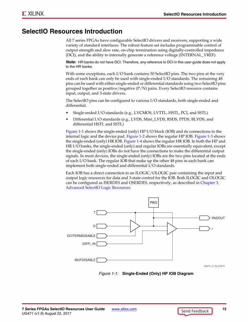
Figure 1-1 shows the single-ended (only) HP I/O block (IOB) and its connections to the internal logic and the device pad. Figure 1-2 shows the regular HP IOB. Figure 1-3 shows the single-ended (only) HR IOB. Figure 1-4 shows the regular HR IOB. In both the HP and HR I/O banks, the single-ended (only) and regular IOBs are essentially equivalent, except the single-ended (only) IOBs do not have the connections to make the differential output signals. In most devices, the single-ended (only) IOBs are the two pins located at the ends of each I/O bank. The regular IOB that make up the other 48 pins in each bank can implement both single-ended and differential I/O standards.
Each IOB has a direct connection to an ILOGIC/OLOGIC pair containing the input and output logic resources for data and 3-state control for the IOB. Both ILOGIC and OLOGIC can be configured as ISERDES and OSERDES, respectively, as described in Chapter 3, Advanced SelectIO Logic Resources.X-Ref Target - Figure 1-1
Figure 1-1: Single-Ended (Only) HP IOB Diagram
UG471_c1_03_010711
PAD
O
T
I
PADOUT
DCITERMDISABLE
DIFFI_IN
IBUFDISABLE
Send Feedback

16 www.xilinx.com 7 Series FPGAs SelectIO Resources User GuideUG471 (v1.9) August 22, 2017
Chapter 1: SelectIO Resources
X-Ref Target - Figure 1-2
Figure 1-2: Regular HP IOB Diagram
X-Ref Target - Figure 1-3
Figure 1-3: Single-Ended (Only) HR IOB Diagram
X-Ref Target - Figure 1-4
Figure 1-4: Regular HR IOB Diagram
UG471_c1_04_010711
PAD
O
T
I
DIFFO_OUT
O_OUT
PADOUT
DCITERMDISABLE
DIFFI_IN
IBUFDISABLE
UG471_c1_05 _011010
PAD
O
T
I
PADOUT
DIFFI_IN
IBUFDISABLE
UG471_c1_06_011110
PAD
O
T
I
DIFFO_OUT
O_OUT
PADOUT
DIFFI_IN
IBUFDISABLE
Send Feedback

7 Series FPGAs SelectIO Resources User Guide www.xilinx.com 17UG471 (v1.9) August 22, 2017
SelectIO Resources General Guidelines
SelectIO Resources General GuidelinesThis section summarizes the general guidelines to be considered when designing with the SelectIO resources in 7 series FPGAs.
7 Series FPGA I/O Bank RulesIn 7 series devices, an I/O bank consists of 50 IOBs. The number of banks depends upon the device size and the package pinout. In the 7 Series FPGAs Overview the total number of available I/O banks is listed by device type. For example, the XC7K325T has 10 usableI/O banks. Figure 1-5 is an example of a columnar floorplan showing the XC7K325T I/O banks. UG475: 7 Series FPGAs Packaging and Pinout Specifications includes information on the I/O banks for each device/package combination.X-Ref Target - Figure 1-5
Figure 1-5: 7 Series FPGA XC7K325T I/O Banks
UG471_c1_07_032111
Bank 18HR
50 I/0
Bank 17HR
50 I/0
Bank 16HR
50 I/0
Bank 15HR
50 I/0
Bank 14HR
50 I/0
Bank 13HR
50 I/0
Bank 34HP
50 I/0
Bank 33HP
50 I/0
Bank 12HR
50 I/0
Bank 32HP
50 I/0
Send Feedback

18 www.xilinx.com 7 Series FPGAs SelectIO Resources User GuideUG471 (v1.9) August 22, 2017
Chapter 1: SelectIO Resources
Supply Voltages for the SelectIO Pins
VCCO
The VCCO supply is the primary power supply of the 7 series I/O circuitry. The VCCO (V) columns in Table 1-55 provide the VCCO requirements for each of the supported I/O standards, and illustrate the VCCO requirements for both inputs and outputs as well as the optional internal differential termination circuit. All VCCO pins for a given I/O bank must be connected to the same external voltage supply on the board, and as a result all of the I/O within a given I/O bank must share the same VCCO level. The VCCO voltage must match the requirements for the I/O standards that have been assigned to the I/O bank. An incorrect VCCO voltage can result in loss of functionality or damage to the device. The 7 series power supply requirements, including power-on and power-off sequencing, are described in the 7 series FPGA data sheets.
In HP I/O banks, if the I/O standard voltage requirement is < 1.8V, but a VCCO > 2.5V is applied, the device automatically enters an overvoltage protection mode. Reconfiguring the device with the correct VCCO level restores normal operation.
VREF
Single-ended I/O standards with a differential input buffer require an input reference voltage (VREF). When VREF is required within an I/O bank, the two multi-function VREF pins for the bank must be used as VREF supply inputs. 7 series FPGAs can optionally use an internally generated reference voltage by enabling the INTERNAL_VREF constraint. For more information on this constraint, see 7 Series FPGA SelectIO Attributes/Constraints, page 46.
VCCAUX
The global auxiliary (VCCAUX) supply rail is primarily used for providing power to the various block feature’s interconnect logic inside the 7 series FPGAs. In the I/O banks, VCCAUX is also used to power input buffer circuits for some of the I/O standards. These include all of the single-ended I/O standards at or below 1.8V, and also some of the 2.5V standards (HR I/O banks only). Additionally, the VCCAUX rail provides power to the bank’s differential input buffer circuits used for the differential and VREF I/O standards.
The 7 series power supply requirements, including power-on and power-off sequencing, are described in the 7 series FPGA data sheets.
VCCAUX_IO
The auxiliary I/O (VCCAUX_IO) supply rail is only present in HP I/O banks and provides power to the I/O circuitry. The Kintex-7 and Virtex-7 FPGAs data sheets contain a table titled Maximum Physical Interface (PHY) Rate for Memory Interfaces that references VCCAUX_IO. This table indicates how the VCCAUX_IO pins can be powered at either 1.8V (default), or optionally at 2.0V to achieve higher frequency performance for certain types of memory interfaces. Although this table is designed for memory interfaces, it can also provide guidance on powering VCCAUX_IO for other high-speed single-ended interfaces based on the target bit rates. The table does not apply to LVDS, which uses a different type of driver circuit than the single-ended drivers that are more affected by the VCCAUX_IO level. Thus, for LVDS interfaces, it does not matter which voltage level the VCCAUX_IO rail is powered at. The default value of 1.8V affords a lower-power consumption and provides very close to the same performance in the I/Os. The 2.0V option is available when the slightly-increased performance is required for the very fastest bit rates supported for the single-ended drivers.
Send Feedback

7 Series FPGAs SelectIO Resources User Guide www.xilinx.com 19UG471 (v1.9) August 22, 2017
7 Series FPGA DCI—Only available in the HP I/O banks
There is a design constraint for I/O nets and primitives called VCCAUX_IO, which should be specified in the design if the VCCAUX_IO pins for any banks are to be set at 2.0V. See 7 Series FPGA SelectIO Attributes/Constraints, page 46 for information on this constraint.
The VCCAUX_IO pins are connected together internally inside Kintex-7 and Virtex-7 device packages in groups of three or four HP I/O banks. The package files chapter of UG475: 7 Series FPGA Packaging and Pinout Specification contains links to the ASCII package files, and the figures in the device diagrams chapter indicate which device/package combinations contain HP I/O banks with VCCAUX_IO pins. The ASCII package files indicate which bank’s VCCAUX_IO pins are grouped together inside the package. The VCCAUX_IO package pin names have the syntax VCCAUX_IO_G#, where the # is the internal group number. The package files contain a column called “VCCAUX Group” that shows for every I/O pin which VCCAUX group that I/O bank is associated with. All I/O pins that are in the same VCCAUX_IO group must have VCCAUX_IO constraints on their nets or primitives that are compatible. All VCCAUX_IO pins that are grouped together should be tied to the same voltage rail on the board. FBG packages for Kintex-7 devices contain VCCAUX_IO pins but are no connects internally. All HP I/O banks in those packages are powered from the main VCCAUX rail instead.
State of I/Os During and After Configuration
7 series FPGAs have pins dedicated to configuration functions contained in I/O bank 0. Banks 14 and 15 also contain I/O pins known as multi-function or multi-purpose pins that can also be used for configuration, but then convert to normal I/O pins after configuration is complete. Additionally in SSI devices, pins in banks 11, 12, 17, 18, 20, and 21 have restrictions during configuration similar to multi-function pins. However, pins in these banks do not have any configuration functions.
In devices where bank 14 and/or bank 15 are HR banks and configured with a VCCO requirement < 1.8V, inputs might have a 0-1-0 transition to the interconnect logic during configuration if the input is tied to 0 or floating and the configuration voltage is > 2.5V. For further details, refer to UG470: 7 Series FPGAs Configuration User Guide.
7 Series FPGA DCI—Only available in the HP I/O banks
IntroductionAs FPGAs get bigger and system clock speeds get faster, PC board design and manufacturing becomes more difficult. With ever faster edge rates, maintaining signal integrity becomes a critical issue. PC board traces must be properly terminated to avoid reflections or ringing.
To terminate a trace, resistors are traditionally added to make the output and/or input match the impedance of the receiver or driver to the impedance of the trace. However, due to increased device I/Os, adding resistors close to the device pins increases the board area and component count, and can in some cases be physically impossible. To address these issues and to achieve better signal integrity, Xilinx developed the digitally controlled impedance (DCI) technology.
Depending on the I/O standard, DCI can either control the output impedance of a driver, or add a parallel termination present at the driver and/or receiver, with the goal of accurately matching the characteristic impedance of the transmission line. DCI actively adjusts these impedances inside the I/O to calibrate to external precision reference resistors placed on the VRN and VRP pins. This compensates for changes in I/O
Send Feedback

20 www.xilinx.com 7 Series FPGAs SelectIO Resources User GuideUG471 (v1.9) August 22, 2017
Chapter 1: SelectIO Resources
impedance due to process variation. It also continuously adjusts the impedances to compensate for variations of temperature and supply voltage fluctuations.
For the I/O standards with controlled impedance drivers, DCI controls the driver impedance to either match the two reference resistors, or for some standards, to match half the value of these reference resistors.
For the I/O standards with controlled parallel termination, DCI provides the parallel termination for both transmitters and receivers. This eliminates the need for termination resistors on the board, reduces board routing difficulties and component count, and improves signal integrity by eliminating stub reflection. Stub reflection occurs when termination resistors are located too far from the end of the transmission line. With DCI, the termination resistors are as close as possible to the output driver or the input buffer, thus, eliminating stub reflections. DCI is only available in 7 series FPGAs HP I/O banks. DCI is not available in HR I/O banks.
Xilinx DCIDCI uses two multi-purpose reference pins in each I/O bank to control the impedance of the driver or the parallel-termination value for all of the I/Os of that bank. The N reference pin (VRN) must be pulled up to VCCO by a reference resistor, and the P reference pin (VRP) must be pulled down to ground by another reference resistor. The value of each reference resistor should be either equal to the characteristic impedance of the PC board traces or twice that value.
To implement DCI in a design:
1. Assign one of the DCI I/O standards in an HP I/O bank (see Table 1-2 and Table 1-3).
2. Connect the VRN multi-function pin to a precision resistor tied to the VCCO rail for the same bank.
3. Connect the VRP multi-function pin to a precision resistor tied to ground.
The following sections discuss how to determine the precision resistor values for VRN and VRP for the different I/O standards. Only one set of VRN and VRP resistors is used for each bank, so all DCI standards within each bank must be able to share the same external resistance values. If several I/O banks in the same I/O bank column are using DCI, and all of those I/O banks use the same VRN/VRP resistor values, the internal VRN and VRP nodes can be cascaded so that only one pair of pins for all of the I/O banks in the entire I/O column is required to be connected to precision resistors. This option is called DCI cascading and is detailed in DCI Cascading, page 22. This section also describes how to determine if I/O banks share the same I/O bank column. If DCI I/O standards are not used in the bank, these pins are available as regular I/O pins. UG475: 7 Series FPGAs Packaging and Pinout Specifications gives detailed pin descriptions.
DCI adjusts the impedance of the I/O by selectively turning transistors in the I/Os on or off. The impedance is adjusted to match the external reference resistors. The adjustment starts during the device startup sequence. By default, the DONE pin does not go High until the first part of the impedance adjustment process is completed.
The DCI calibration can be reset by instantiating the DCIRESET primitive. Toggling the RST input to the DCIRESET primitive while the device is operating, resets the DCI state machine and restarts the calibration process. All I/Os using DCI will be unavailable until the LOCKED output from the DCIRESET block is asserted. This functionality is useful in applications where the temperature and/or supply voltage changes significantly from device power-up to the nominal operating condition.
Send Feedback

7 Series FPGAs SelectIO Resources User Guide www.xilinx.com 21UG471 (v1.9) August 22, 2017
7 Series FPGA DCI—Only available in the HP I/O banks
For controlled impedance output drivers, the impedance can be adjusted either to match the reference resistors or half the resistance of the reference resistors. For on-chip termination, the termination is always adjusted to match the reference resistors.
For the I/O standards that support the DCI controlled impedance driver, DCI can configure output drivers to be the following types:
• Controlled Impedance Driver (Source Termination)
• Controlled Impedance Driver with Half Impedance (Source Termination)
For the I/O standards that support parallel termination, DCI creates a Thevenin equivalent, or split-termination resistance, to the VCCO/2 voltage level. The I/O standards' naming convention adds:
• DCI in the name of the I/O standard if split-termination resistors are always present in the I/O, independent of whether the standard is used on an input, output, or bidirectional pin.
• T_DCI in the name of the I/O standard if split-termination resistors are only present when the output buffer is 3-stated.
Match_cycle Configuration OptionMatch_cycle is a configuration option that optionally halts the startup sequence at the end of the FPGA configuration sequence until the DCI logic has performed the first match (calibration) to the external reference resistors. This option is also sometimes referred to as DCI match. For more information about the Match_cycle option, refer to the “Configuration Details” chapter in UG470: 7 Series FPGAs Configuration User Guide. For information on how to invoke the option in a design and to set it to a specific startup cycle, refer to the Match_cycle option in UG628: Command Line Tools User Guide.
DCIUpdateMode Configuration OptionDCIUpdateMode is a configuration option that can override control of how often the DCI circuit updates the impedance matching to the VRN and VRP reference resistors. This option defaults to AsRequired but also has an optional value of Quiet in the Xilinx implementation software. The settings for the DCIUpdateMode configuration option are:
• AsRequired: Initial impedance calibration is made at device initialization, and dynamic impedance adjustments are made as needed throughout device operation (default).
• Continuous: For 7 series FPGAs, this value has no effect (defaults back to AsRequired).
• Quiet: Impedance calibration is done only once at device initialization, or each time the RST pin is asserted on the DCIRESET primitive for designs that include this primitive.
It is strongly recommended that the DCIUpdateMode option be kept with the default value of AsRequired so that the DCI circuitry is allowed to operate normally. See UG628: Command Line Tools User Guide for more details if there is a special need to set this option to Quiet.
Send Feedback

22 www.xilinx.com 7 Series FPGAs SelectIO Resources User GuideUG471 (v1.9) August 22, 2017
Chapter 1: SelectIO Resources
DCIRESET PrimitiveDCIRESET is a Xilinx design primitive that provides the capability to perform a reset of the DCI controller state machine during normal operation of the design. Unless DCIUpdateMode is set to Quiet (see DCIUpdateMode Configuration Option) or for the case outlined below related to the use of multi-function pins set to use DCI, for most situations this primitive should not be required in a design. See UG768: Xilinx 7 Series FPGA Libraries Guide for HDL Designs for more details on the DCIRESET primitive.
Special DCI Requirements for Some BanksIf any of the multi-function pins in I/O banks 14 or 15 (any device), or banks 11, 12, 17, 18, 20, and 21 (SSI devices only) are assigned DCI I/O standards in the user design, the DCIRESET primitive should also be included and used in the design. In that case, the design should pulse the RST input of DCIRESET and then wait for the LOCKED signal to be asserted prior to using any user input or outputs on these pins with DCI standards. This is required because these I/O pins ignore the initial DCI calibration that happens during the normal device initialization.
As a result, if the DCIRESET primitive had not been used and DCIUpdateMode was set to AsRequired, after those pins become normal I/O pins there would be an indeterministic delay between the end of configuration and when the DCI calibration algorithm updated those pins DCI settings. If DCIRESET was not used and DCIUpdateMode was set to Quiet, these pins would never have their DCI values set. In that case, the Controlled Impedance DCI I/O standards (such as LVDCI_18) would behave as if in the high-Z state all the time, and Split Termination DCI I/O standards (such as SSTL15_DCI) would behave as if there was no internal termination. Including and using the DCIRESET primitive in the design allows these pins to have DCI I/O standards and to perform without issue.
DCI CascadingThe 7 series FPGA HP I/O banks using DCI I/O standards have the option of deriving the DCI impedance values from another HP I/O bank. As shown in Figure 1-6, a digital control bus is internally distributed throughout the bank to control the impedance of each I/O.
With DCI cascading, one I/O bank (the master bank) must have its VRN/VRP pins connected to external reference resistors. Other I/O banks in the same HP I/O bank column (slave banks) can use DCI standards with the same impedance as the master bank, without connecting the VRN/VRP pins on these slave banks to external resistors. DCI impedance control in cascaded banks is received from the I/O master bank.
X-Ref Target - Figure 1-6
Figure 1-6: DCI Use within a Bank
UG471_c1_08_101810
DCI VRN/VRP
From Bank Above
From Bank Below
ToLocalBank
Send Feedback

7 Series FPGAs SelectIO Resources User Guide www.xilinx.com 23UG471 (v1.9) August 22, 2017
7 Series FPGA DCI—Only available in the HP I/O banks
Figure 1-7 shows DCI cascading support over multiple I/O banks. Bank B is the masterI/O bank, and Banks A and C are considered slave I/O banks.X-Ref Target - Figure 1-7
Figure 1-7: DCI Cascading Supported Over Multiple I/O Banks
UG471_c1_09_011811
DCI VRN/VRP
Bank A
Bank B
Bank C
ToLocalBank
ToLocalBank
ToLocalBank
To Banks Above (When Cascaded)
To Banks Below(When Cascaded)
Send Feedback

24 www.xilinx.com 7 Series FPGAs SelectIO Resources User GuideUG471 (v1.9) August 22, 2017
Chapter 1: SelectIO Resources
The guidelines when using DCI cascading are as follows:
• DCI cascading is only available through a column of HP I/O banks
• The master and slave SelectIO banks must all reside on the same HP I/O column on the device and can span the entire column unless there is an interposer boundary.
• DCI cascading cannot pass through the interposer boundaries of the larger Virtex-7 devices with stacked silicon interconnect (SSI) technology. This includes the XC7V2000T and XC7VX1140T devices. For these devices, the I/O banks that are separated by these interposer boundaries are shown in the figures of the “Die Level Bank Numbering Overview” section of UG475: 7 Series FPGAs Packaging and Pinout Specifications.
• Master and slave I/O banks must have the same VCCO and VREF (if applicable) voltage.
• I/O banks in the same HP I/O column that are not using DCI (pass-through banks) do not have to comply with the VCCO and VREF voltage rules for combining DCI settings.
• DCI I/O banking compatibility rules must be satisfied across all master and slave banks (for example, only one DCI I/O standard using single termination type is allowed across all master and slave banks).
• To locate I/O banks that reside in the same I/O column, refer to the figures of the “Die Level Bank Numbering Overview” section of UG475: 7 Series FPGAs Packaging and Pinout Specifications.
• For specific information on implementing DC cascading in a design, see DCI_CASCADE Constraint, page 46.
• Xilinx recommends that unused banks be powered up because leaving the VCCO pins of unused I/O banks floating reduces the level of ESD protection on these pins and the I/O pins in the bank. If the bank is unpowered, DCI can still be cascaded through the unpowered bank.
Send Feedback

7 Series FPGAs SelectIO Resources User Guide www.xilinx.com 25UG471 (v1.9) August 22, 2017
7 Series FPGA DCI—Only available in the HP I/O banks
Controlled Impedance Driver (Source Termination)To optimize signal integrity for high-speed or high-performance applications, extra measures are required to match the output impedance of drivers to the impedance of the transmission lines and receivers. Optimally, drivers must have an output impedance matching the characteristic impedance of the driven line, otherwise reflections can occur due to discontinuities. To solve this issue, designers sometimes use external-source series-termination resistors placed close to the pins of high-strength, low-impedance drivers. The resistance values are chosen such that the sum of the driver's output impedance plus the resistance of the source series-termination resistor roughly equals the impedance of the transmission line.
DCI can provide controlled impedance output drivers to eliminate reflections without requiring the use of an external source-termination resistor. The impedance is set by the external reference resistors with resistance equal to the trace impedance.
The DCI I/O standards supporting the controlled impedance driver are: LVDCI_15, LVDCI_18, HSLVDCI_15, HSLVDCI_18, HSUL_12_DCI, and DIFF_HSUL_12_DCI. Figure 1-8 illustrates a controlled impedance driver in a 7 series device.
Controlled Impedance Driver with Half Impedance (Source Termination)DCI also provides drivers with one half of the impedance of the reference resistors. This doubling of the reference resistor value reduces the static power consumption through these resistors by a factor of half. The DCI I/O standards supporting controlled impedance drivers with half-impedance are LVDCI_DV2_15 and LVDCI_DV2_18.
Figure 1-9 illustrates a controlled driver with half impedance inside a 7 series device. The reference resistors R must be 2 × Z0 in order to match the impedance of Z0.
X-Ref Target - Figure 1-8
Figure 1-8: Controlled Impedance Driver
UG471_c1_10_101810
IOBR
7 Series FPGAHP Bank DCI
Z0
X-Ref Target - Figure 1-9
Figure 1-9: Controlled Impedance Driver with Half Impedance
UG471_c1_11_101810
IOBR/2
7 Series FPGAHP Bank DCI
Z0
Send Feedback

26 www.xilinx.com 7 Series FPGAs SelectIO Resources User GuideUG471 (v1.9) August 22, 2017
Chapter 1: SelectIO Resources
Split-Termination DCI (Thevenin Equivalent Termination to VCCO/2)Some I/O standards (e.g., HSTL and SSTL) require an input termination resistance (R) to a VTT voltage of VCCO/2 (see Figure 1-10).
Split-termination DCI creates a Thevenin equivalent circuit using two resistors of twice the resistance value (2R). One terminates to VCCO, the other to ground. Split-termination DCI provides an equivalent termination to VCCO/2 using this method. The 2R termination resistance is set by the external reference resistors. For example, to achieve the Thevenin equivalent parallel-termination circuit of 50Ω to VCCO/2, would require 100Ω external precision resistors at the VRN and VRP pins. The DCI input standards supporting split termination are shown in Table 1-2.
X-Ref Target - Figure 1-10
Figure 1-10: Input Termination to VCCO/2 without DCI
R
UG471_c1_12_011811
VCCO/2
VREF
IOB
Z0
7 Series FPGA
Table 1-2: All DCI I/O Standards Supporting Split-Termination DCI
HSTL_I_DCI DIFF_HSTL_I_DCI SSTL18_I_DCI DIFF_SSTL18_I_DCI
HSTL_I_DCI_18 DIFF_HSTL_I_DCI_18 SSTL18_II_DCI DIFF_SSTL18_II_DCI
HSTL_II_DCI DIFF_HSTL_II_DCI SSTL18_II_T_DCI DIFF_SSTL18_II_T_DCI
HSTL_II_DCI_18 DIFF_HSTL_II_DCI_18 SSTL15_DCI DIFF_SSTL15_DCI
HSTL_II_T_DCI DIFF_HSTL_II_T_DCI SSTL15_T_DCI DIFF_SSTL15_T_DCI
HSTL_II_T_DCI_18 DIFF_HSTL_II_T_DCI_18 SSTL135_DCI DIFF_SSTL135_DCI
SSTL135_T_DCI DIFF_SSTL135_T_DCI
SSTL12_DCI DIFF_SSTL12_DCI
SSTL12_T_DCI DIFF_SSTL12_T_DCI
Send Feedback

7 Series FPGAs SelectIO Resources User Guide www.xilinx.com 27UG471 (v1.9) August 22, 2017
7 Series FPGA DCI—Only available in the HP I/O banks
Figure 1-11 illustrates split-termination DCI inside a 7 series device.
VRN/VRP External Resistance Design Migration GuidelinesPrevious Xilinx FPGA families featuring DCI used a slightly different circuit for calibrating the split-termination impedance from the external reference resistors placed on the VRN and VRP pins. The Virtex-6 FPGA DCI calibrates each leg of the split-termination circuit to be double the external resistor values. For example, in a Virtex-6 device with a target parallel termination of 50Ω to VCCO/2 requires 50Ω external resistors on the VRN and VRP pins.
The 7 series FPGAs DCI calibrates each leg of the split termination circuit to be directly equal to the external resistor values. For example, in a 7 series device with a target parallel termination of 50Ω to VCCO/2 requires 100Ω external resistors on the VRN and VRP pins. This is particularly important to consider when choosing the VRN and VRP values to be used in the same I/O bank (or multiple cascaded DCI banks) for both controlled-impedance DCI and split-termination DCI standards.
In a Virtex-6 FPGA design with a 50Ω target controlled impedance driver for an LVDCI_18 output and a 50Ω target split-termination receiver for an HSTL_I_DCI_18 input, can be implemented using 50Ω external resistors on the VRN and VRP pins. To migrate this same design to a 7 series FPGA would not change the HSTL_I_DCI_18 I/O standard; however, the external resistors must change to 100Ω and the controlled impedance driver changes to an LVDCI_DIV2_18 output. This example outcome is equivalent; however both resistor values and I/O standard changes are required. A power rating of 0.05W or higher can be safely used for the VRN and VRP external resistors.
X-Ref Target - Figure 1-11
Figure 1-11: Input Termination to VCCO/2 Using Split-Termination DCI (External Resistors on VRN, VRP = 2R)
2R
2R
UG471_c1_13_011811
VCCO
VREF
IOB
Z0
7 Series FPGA HP Bank DCI
Send Feedback

28 www.xilinx.com 7 Series FPGAs SelectIO Resources User GuideUG471 (v1.9) August 22, 2017
Chapter 1: SelectIO Resources
DCI and 3-state DCI (T_DCI)The class-I driver versions of the SSTL and HSTL I/O standards are only supported for unidirectional signaling; they can only be assigned to input-only or output-only pins in a design, not bidirectional pins. The DCI versions of class-I SSTL and HSTL I/O standards only have internal split-termination resistors present on inputs (not outputs). The class-II driver versions of SSTL and HSTL I/O standards are supported for bidirectional and unidirectional signaling; they can be assigned to input, output, or bidirectional pins in a design. The DCI versions of class-II SSTL and HSTL I/O standards always have internal split-termination resistors present on input, outputs, or bidirectional pins. Figure 1-12 illustrates a driver with split termination inside a 7 series device.
When the split-termination is present while driving, DCI only controls the impedance of the termination, but not the driver. However, many applications can benefit from having the split-termination resistors turned off whenever the pin is driving. The 3-state DCI (T_DCI) standards were designed to meet this requirement by turning off the split-termination resistors whenever the output buffer is driving, and turning on the split-termination resistors when the output is in 3-state (such as when receiving or in an idle state). The T_DCI standards can only be assigned to bidirectional pins. For unidirectional input pins, the DCI version of the standard can be assigned. For unidirectional output pins, either the non-DCI or the DCI version can be assigned.
X-Ref Target - Figure 1-12
Figure 1-12: Driver with Termination to VCCO/2 Using DCI Split Termination (External Resistors on VRN, VRP = 2R)
2R
2R
UG471_c1_14_011811
VCCOIOB
Z0
7 Series FPGA HP Bank DCI
Send Feedback

7 Series FPGAs SelectIO Resources User Guide www.xilinx.com 29UG471 (v1.9) August 22, 2017
7 Series FPGA DCI—Only available in the HP I/O banks
The I/O standards with split-termination DCI resistors that are always present are shown in Table 1-3.
The I/O standards with split-termination DCI (T_DCI) that are only enabled when 3-stated are shown in Table 1-4.
Note: The T_DCI standards can only be assigned to bidirectional pins.
DCI in 7 Series FPGAs I/O StandardsDCI supports the standards shown in Table 1-5.
Table 1-3: I/O Standards with Split-Termination DCI Always Present
HSTL_I_DCI(1) DIFF_HSTL_I_DCI(1) SSTL18_I_DCI(1) DIFF_SSTL18_I_DCI(1)
HSTL_I_DCI_18(1) DIFF_HSTL_I_DCI_18(1) SSTL18_II_DCI DIFF_SSTL18_II_DCI
HSTL_II_DCI DIFF_HSTL_II_DCI SSTL15_DCI(1) DIFF_SSTL15_DCI(1)
HSTL_II_DCI_18 DIFF_HSTL_II_DCI_18 SSTL135_DCI(1) DIFF_SSTL135_DCI(1)
SSTL12_DCI(1) DIFF_SSTL12_DCI(1)
Notes: 1. The non-class II versions of the HSTL and SSTL I/O standards only have the split-termination DCI resistors present on inputs, not
outputs. Bidirectional pin assignments are not allowed for these standards.
Table 1-4: I/O Standards with Split-Termination DCI Only When 3-Stated
HSTL_II_T_DCI SSTL18_II_T_DCI DIFF_SSTL18_II_T_DCI
HSTL_II_T_DCI_18 SSTL15_T_DCI DIFF_SSTL15_T_DCI
DIFF_HSTL_II__T_DCI SSTL135_T_DCI DIFF_SSTL135_T_DCI
DIFF_HSTL_II_T_DCI_18 SSTL12_T_DCI DIFF_SSTL12_T_DCI
Table 1-5: All 7 Series Device DCI I/O Standards
LVDCI_18 HSTL_I_DCI DIFF_HSTL_I_DCI SSTL18_I_DCI DIFF_SSTL18_I_DCI
LVDCI_15 HSTL_I_DCI_18 DIFF_HSTL_I_DCI_18 SSTL18_II_DCI DIFF_SSTL18_II_DCI
LVDCI_DV2_18 HSTL_II_DCI DIFF_HSTL_II_DCI SSTL18_II_T_DCI DIFF_SSTL18_II_T_DCI
LVDCI_DV2_15 HSTL_II_DCI_18 DIFF_HSTL_II_DCI_18 SSTL15_DCI DIFF_SSTL15_DCI
HSLVDCI_18 HSTL_II_T_DCI DIFF_HSTL_II_T_DCI SSTL15_T_DCI DIFF_SSTL15_T_DCI
HSLVDCI_15 HSTL_II_T_DCI_18 DIFF_HSTL_II_T_DCI_18 SSTL135_DCI DIFF_SSTL135_DCI
SSTL135_T_DCI DIFF_SSTL135_T_DCI
SSTL12_DCI DIFF_SSTL12_DCI
SSTL12_T_DCI DIFF_SSTL12_T_DCI
HSUL_12_DCI DIFF_HSUL_12_DCI
Send Feedback

30 www.xilinx.com 7 Series FPGAs SelectIO Resources User GuideUG471 (v1.9) August 22, 2017
Chapter 1: SelectIO Resources
To correctly use DCI in 7 series devices:
1. VCCO pins must be connected to the appropriate VCCO voltage based on the IOSTANDARDs in that I/O bank.
2. Correct DCI I/O buffers must be used in the software either by using IOSTANDARD attributes or instantiations in the HDL code.
3. DCI standards require connecting external reference resistors to the multipurpose pins (VRN and VRP). When this is required, these two multipurpose pins cannot be used as general-purpose I/O in the I/O bank using DCI or in the master I/O bank when cascading DCI. Refer to the 7 series FPGA pinout tables for the specific pin locations. Pin VRN must be pulled up to VCCO by its reference resistor. Pin VRP must be pulled down to ground by its reference resistor. An exception to this requirement comes when cascading DCI in slave I/O banks since the VRN and VRP pins can be used as general-purpose I/O.
DCI standards with the controlled impedance driver can be used on input-only signals. For this case, if these pins are the only pins using DCI standards in a given I/O bank, that bank does not require connecting the external reference resistors to the VRP/VRN pins. When these DCI-based I/O standards are the only ones in a bank, the VRP and VRN pins in that bank can be used as general-purpose I/O.
• DCI inputs that do not require reference resistors on VRP/VRN are shown in Table 1-6.
4. The value of the external reference resistors should be selected to give the desired output driver impedance or split-termination impedance. For example, when using LVDCI_15, to achieve a 50Ω output driver impedance, the external reference resistors used on the VRN and VRP pins should each be 50Ω. When using SSTL15_T_DCI, to achieve a 50Ω Thevenin equivalent termination (R) to VCCO/2, the external reference resistors should each be 100Ω, which is (2R). Xilinx requires that the exact same value of the resistance be used on the VRP and VRN pins in order to achieve the expected DCI behavior.
5. Follow the DCI I/O banking rules:
a. VREF must be compatible for all of the inputs in the same I/O bank or in a group of I/O banks when using DCI cascade.
b. VCCO must be compatible for all of the inputs and outputs in the same I/O bank.
c. Split termination, controlled impedance driver, and controlled impedance driver with half impedance can co-exist in the same bank.
Table 1-6: I/O Standards with DCI Inputs that Do Not Require Reference Resistors
LVDCI_18 LVDCI_DV2_18 HSLVDCI_18 HSUL_12_DCI
LVDCI_15 LVDCI_DV2_15 HSLVDCI_15 DIFF_HSUL_12_DCI
Send Feedback

7 Series FPGAs SelectIO Resources User Guide www.xilinx.com 31UG471 (v1.9) August 22, 2017
7 Series FPGA DCI—Only available in the HP I/O banks
DCI Usage Examples• Figure 1-13 provides examples illustrating the use of the HSTL_I_DCI and
HSTL_II_DCI I/O standards.
• Figure 1-14 provides examples illustrating the use of the SSTL18_I_DCI and SSTL18_II_DCI I/O standards.
X-Ref Target - Figure 1-13
Figure 1-13: HSTL DCI Usage Examples
R R
2R
2R
R
2R
R 2R
2R
2R 2R
2R
UG471_c1_15_011811
Conventional
DCI TransmitConventionalReceive
ConventionalTransmitDCI Receive
DCI TransmitDCI Receive
Bidirectional
ReferenceResistor
Recommended Z0
VRN = VRP = 2R = 2Z0
50Ω
VRN = VRP = 2R = 2Z0
50Ω
HSTL_I HSTL_II
N/A
Z0
R
R
2R
2R
2R
2R
Z0
Z0Z0
Z0 Z0
Z0Z0
7 Series FPGAHP Bank DCI
7 Series FPGAHP Bank DCI
7 Series FPGAHP Bank DCI
7 Series FPGAHP Bank DCI
7 Series FPGAHP Bank DCI
7 Series FPGAHP Bank DCI
7 Series FPGAHP Bank DCI
7 Series FPGAHP Bank DCI 7 Series FPGA
HP Bank DCI
Z0
2R
2R
2R
2R
VCCO/2
VCCO/2
VCCO/2
VCCO/2
VCCO/2 VCCO/2
VCCOVCCO
VCCOVCCO
VCCOVCCOVCCO
VCCO
Notes:1. Z0 is the recommended PCB trace impedance.
Send Feedback

32 www.xilinx.com 7 Series FPGAs SelectIO Resources User GuideUG471 (v1.9) August 22, 2017
Chapter 1: SelectIO Resources
X-Ref Target - Figure 1-14
Figure 1-14: SSTL DCI Usage Examples
ug471_c1_16_042413
SSTL18_I SSTL18_II
R R
2R
2R
R
2R
R 2R
2R
2R 2R
2R
Conventional
DCI TransmitConventionalReceive
ConventionalTransmitDCI Receive
DCI TransmitDCI Receive
Bidirectional
ReferenceResistor
Recommended Z0
VRN = VRP = 2R = 2Z0
50Ω
VRN = VRP = 2R = 2Z0
50Ω
N/A
Z0
R
R
2R
2R
2R
2R
Z0
Z0Z0
Z0 Z0
Z0Z0
7 Series FPGAHP Bank DCI
7 Series FPGAHP Bank DCI
7 Series FPGAHP Bank DCI
7 Series FPGAHP Bank DCI
7 Series FPGAHP Bank DCI
7 Series FPGAHP Bank DCI
7 Series FPGAHP Bank DCI
7 Series FPGAHP Bank DCI 7 Series FPGA
HP Bank DCI
Z0
2R
2R
2R
2R
VCCO/2
VCCO/2
VCCO/2
VCCO/2
VCCO/2 VCCO/2
VCCOVCCO
VCCOVCCO
VCCOVCCOVCCO
VCCO
Notes:1. Z0 is the recommended PCB trace impedance.
Send Feedback

7 Series FPGAs SelectIO Resources User Guide www.xilinx.com 33UG471 (v1.9) August 22, 2017
Uncalibrated Split Termination in High-Range I/O Banks (IN_TERM)
Uncalibrated Split Termination in High-Range I/O Banks (IN_TERM)The HR I/O banks have an optional on-chip split-termination feature very similar to the 3-state split-termination DCI feature available in the HP I/O banks. Similar to the 3-state split-termination DCI in the HP banks, the option in the HR banks creates a Thevenin equivalent circuit using two internal resistors of twice the target resistance value. One resistor terminates to VCCO and the other to ground, providing a Thevenin equivalent termination circuit to the mid-point VCCO/2. The termination is present constantly on inputs, and on bidirectional pins whenever the output buffer is 3-stated. However, an important difference between this uncalibrated split-termination option and 3-state split-termination DCI is that instead of calibrating to external reference resistors on the VRN and VRP pins when using DCI, this feature invokes internal resistors that have no calibration routine to compensate for temperature, process, or voltage variations. This option has target Thevenin equivalent resistance values of 40Ω, 50Ω, and 60Ω.
Another difference from the DCI termination is how this uncalibrated termination is invoked in a design. While the 3-state split-termination DCI option is invoked by assigning the T_DCI I/O standards to I/O pins in HP I/O banks, the uncalibrated split-termination option is invoked by assigning IN_TERM constraints to the I/O pin nets in HR I/O banks. This can be done in several ways, including in the source HDL design, in the UCF, NCF, or XCF files, or in the PlanAhead™ software. For more details, see IN_TERM in UG625: Constraints Guide (for the ISE® tools) or UG912: Vivado Design Suite Properties Reference Guide.
In HR banks, the IN_TERM constraint can be set to NONE (default), UNTUNED_SPLIT_40, UNTUNED_SPLIT_50, or UNTUNED_SPLIT_60. An example of the UCF syntax is:
NET "pad_net_name"IN_TERM = "UNTUNED_SPLIT_50";
Table 1-7 shows a list of I/O standards that support the IN_TERM constraint in the HR I/O banks. IN_TERM is not supported in HP I/O banks.
Table 1-7: I/O Standards that Support IN_TERM
HSTL_I DIFF_HSTL_I SSTL15_R DIFF_SSTL15_R
HSTL_II DIFF_HSTL_II SSTL15 DIFF_SSTL15
HSTL_I_18 DIFF_HSTL_I_18 SSTL135_R DIFF_SSTL135_R
HSTL_II_18 DIFF_HSTL_II_18 SSTL135 DIFF_SSTL135
SSTL18_I DIFF_SSTL18_I
SSTL18_II DIFF_SSTL18_II
Send Feedback

34 www.xilinx.com 7 Series FPGAs SelectIO Resources User GuideUG471 (v1.9) August 22, 2017
Chapter 1: SelectIO Resources
7 Series FPGA SelectIO PrimitivesThe Xilinx software library includes an extensive list of primitives to support a variety of I/O standards available in the 7 series FPGA I/O primitives. The following generic primitives can each support most of the available single-ended I/O standards.
• IBUF (input buffer)
• IBUF_IBUFDISABLE (input buffer with buffer disable control)
• IBUF_INTERMDISABLE (input buffer with buffer disable and IN_TERM disable controls)
• IBUFG (clock input buffer)
• IOBUF (bidirectional buffer)
• IOBUF_DCIEN (bidirectional buffer with DCI disable and input buffer disable)
• IOBUF_INTERMDISABLE (bidirectional buffer with IN_TERM disable and input buffer disable)
• OBUF (output buffer)
• OBUFT (3-state output buffer)
These eight generic primitives can each support most of the available differential I/O standards:
• IBUFDS (differential input buffer)
• IBUFDS_DIFF_OUT (differential input buffer with complementary outputs)
• IBUFDS_DIFF_OUT_IBUFDISABLE (differential input buffer with complementary outputs and buffer disable)
• IBUFDS_DIFF_OUT_INTERMDISABLE (differential input buffer with complementary outputs, buffer disable, and IN_TERM disable)
• IBUFDS_IBUFDISABLE (differential input buffer with buffer disable control)
• IBUFDS_INTERMDISABLE (differential input buffer with buffer disable, and IN_TERM disable)
• IBUFGDS (differential clock input buffer)
• IBUFGDS_DIFF_OUT (differential clock input buffer with complementary outputs)
• IOBUFDS (differential bidirectional buffer)
• IOBUFDS_DCIEN (differential bidirectional buffer with DCI disable and input buffer disable)
• IOBUFDS_DIFF_OUT (differential bidirectional buffer with complementary outputs from the input buffer)
• IOBUFDS_DIFF_OUT_DCIEN (differential bidirectional buffer with complementary outputs from the input buffer, with DCI disable and input buffer disable)
• IOBUFDS_DIFF_OUT_INTERMDISABLE (differential bidirectional buffer with complementary outputs from the input buffer with IN_TERM disable and buffer disable)
• IOBUFDS_INTERMDISABLE (differential bidirectional buffer with buffer disable and IN_TERM disable)
• OBUFDS (differential output buffer)
• OBUFTDS (differential 3-state output buffer)
Send Feedback

7 Series FPGAs SelectIO Resources User Guide www.xilinx.com 35UG471 (v1.9) August 22, 2017
7 Series FPGA SelectIO Primitives
More information including instantiation techniques and available attributes for these and all other design primitives is available in UG768: Xilinx 7 Series FPGA Libraries Guide for HDL Designs.
IBUF and IBUFGSignals used as inputs to 7 series devices must use an input buffer (IBUF). The generic 7 series FPGA IBUF primitive is shown in Figure 1-15.
The IBUF and IBUFG primitives are the same. IBUFGs are used when an input buffer is used as a clock input. In the Xilinx software tools, an IBUFG is automatically placed at clock input sites.
IBUF_IBUFDISABLEThe IBUF_IBUFDISABLE primitive shown in Figure 1-16 is an input buffer with a disable port that can be used as an additional power saving feature for periods when the input is not used.
The IBUF_IBUFDISABLE primitive can disable the input buffer and force the O output to the fabric to a logic High when the USE_IBUFDISABLE attribute is set to TRUE and the IBUFDISABLE signal is asserted High. If USE_IBUFDISABLE is set to FALSE, this input is ignored and should be tied to ground. This feature can be used to reduce power at times when the I/O is idle. Input buffers that use the VREF power rail (such as SSTL and HSTL) benefit the most from the IBUFDISABLE being set to TRUE because they tend to have higher static power consumption than the non-VREF standards such as LVCMOS and LVTTL.
X-Ref Target - Figure 1-15
Figure 1-15: Input Buffer Primitives (IBUF/IBUFG)
ug471_c1_17_011811
IBUF/IBUFG
O (Output)into FPGA
I (Input)From device pad
X-Ref Target - Figure 1-16
Figure 1-16: Input Buffer With Input Buffer Disable (IBUF_IBUFDISABLE)
IBUF_IBUFDISABLE
IBUFDISABLE
I O
UG471_c1_63_041412
Send Feedback

36 www.xilinx.com 7 Series FPGAs SelectIO Resources User GuideUG471 (v1.9) August 22, 2017
Chapter 1: SelectIO Resources
IBUF_INTERMDISABLEThe IBUF_INTERMDISABLE primitive shown in Figure 1-17 is available in the HR I/O banks and is similar to the IBUF_IBUFDISABLE primitive in that it has a IBUFDISABLE port that can be used to disable the input buffer during periods that the buffer is not being used. The IBUF_INTERMDISABLE primitive also has an INTERMDISABLE port that can be used to disable the optional uncalibrated split-termination feature. See Uncalibrated Split Termination in High-Range I/O Banks (IN_TERM) for more details about this feature.
The IBUF_INTERMDISABLE primitive can disable the input buffer and force the O output to the fabric to a logic High when the USE_IBUFDISABLE attribute is set to TRUE and the IBUFDISABLE signal is asserted High. If USE_IBUFDISABLE is set to FALSE, this input is ignored and should be tied to ground. If the I/O is using the optional uncalibrated split-termination feature (IN_TERM), those termination legs are disabled whenever the driver is active (T is low). The IBUF_INTERMDISABLE primitive further allows the termination legs to be disabled whenever the INTERMDISABLE signal is asserted High. These features can be combined to reduce power whenever the input is idle. Input buffers that use the VREF power rail (such as SSTL and HSTL) benefit the most from the IBUFDISABLE signal being set to TRUE because they tend to have higher static power consumption than the non-VREF standards such as LVCMOS and LVTTL.
IBUFDS and IBUFGDSThe usage and rules corresponding to the differential primitives are similar to the single-ended SelectIO primitives. Differential SelectIO primitives have two pins to and from the device pads to show the P and N channel pins in a differential pair. N channel pins have a B suffix. The IBUFDS and IBUFGDS primitives are the same, IBUFGDS is used when an differential input buffer is used as a clock input.
Figure 1-18 shows the differential input buffer primitive.
X-Ref Target - Figure 1-17
Figure 1-17: Input Buffer With Input Buffer Disable and IN_TERM Disable (IBUF_INTERMDISABLE)
IBUF_INTERMDISABLE
IBUFDISABLE
INTERMDISABLE
I O
UG471_c1_64_041412
X-Ref Target - Figure 1-18
Figure 1-18: Differential Input Buffer Primitives (IBUFDS/IBUFGDS)
ug471_c1_21_041112
+
–
I
IB
O
IBUFDS/IBUFGDS
Inputs fromdevice pads
Output toFPGA
Send Feedback

7 Series FPGAs SelectIO Resources User Guide www.xilinx.com 37UG471 (v1.9) August 22, 2017
7 Series FPGA SelectIO Primitives
IBUFDS_DIFF_OUT and IBUFGDS_DIFF_OUTFigure 1-19 shows the differential input buffer primitives with complementary outputs(O and OB). IBUFDS_DIFF_OUT and IBUFGDS_DIFF_OUT primitives are the same, IBUFGDS_DIFF_OUT is used for clock inputs. These primitives are only recommended for use by experienced Xilinx designers.
IBUFDS_DIFF_OUT_IBUFDISABLEThe IBUFDS_DIFF_OUT_IBUFDISABLE primitive shown in Figure 1-20 is a differential input buffer with complementary differential outputs and a disable port that can be used as an additional power saving feature for periods when the input is not used.
The IBUFDS_DIFF_OUT_IBUFDISABLE primitive can disable the input buffer and force both the O and OB outputs to the fabric high when the USE_IBUFDISABLE attribute is set to TRUE and the IBUFDISABLE signal is asserted High. If USE_IBUFDISABLE is set to FALSE, this input is ignored and should be tied to ground. This feature can be used to reduce power whenever the I/O is idle.
IBUFDS_IBUFDISABLEThe IBUFDS_IBUFDISABLE primitive shown in Figure 1-21 is a differential input buffer with a disable port that can be used as an additional power saving feature for periods when the input is not used.
X-Ref Target - Figure 1-19
Figure 1-19: Differential Input Buffer Primitives With Complementary Outputs(IBUFDS_DIFF_OUT/IBUFGDS_DIFF_OUT)
ug471_c1_25_041112
+
– OB
OI
IB
IBUFDS_DIFF_OUT/IBUFGDS_DIFF_OUT
Input from Device Pad
Output toFPGA
X-Ref Target - Figure 1-20
Figure 1-20: Differential Input Buffer With Complementary Outputs and Input Buffer Disable (IBUFDS_DIFF_OUT_IBUFDISABLE)
IBUFDS_DIFF_OUT_IBUFDISABLE
I
IB OB
O
UG471_c1_67_041412
IBUFDISABLE
Send Feedback

38 www.xilinx.com 7 Series FPGAs SelectIO Resources User GuideUG471 (v1.9) August 22, 2017
Chapter 1: SelectIO Resources
The IBUFDS_IBUFDISABLE primitive can disable the input buffer and force the O output to the fabric to a logic High when the USE_IBUFDISABLE attribute is set to TRUE and the IBUFDISABLE signal is asserted High. If USE_IBUFDISABLE is set to FALSE, this input is ignored and should be tied to ground. This feature can be used to reduce power whenever the I/O is idle.
IBUFDS_INTERMDISABLEThe IBUFDS_INTERMDISABLE primitive shown in Figure 1-22 is available in the HR I/O banks and is similar to the IBUFDS_IBUFDISABLE primitive in that it has an IBUFDISABLE port that can be used to disable the input buffer during periods that the buffer is not being used. The IBUFDS_INTERMDISABLE primitive also has an INTERMDISABLE port that can be used to disable the optional uncalibrated split-termination feature. See Uncalibrated Split Termination in High-Range I/O Banks (IN_TERM) for more details on this feature.
The IBUFDS_INTERMDISABLE primitive can disable the input buffer and force the O output to the fabric High when the USE_IBUFDISABLE attribute is set to TRUE and the IBUFDISABLE signal is asserted High. If USE_IBUFDISABLE is set to FALSE, the IBUFDISABLE input is ignored and should be tied to ground. If the I/O is using the optional uncalibrated split-termination feature (IN_TERM), this primitive disables the termination legs whenever the INTERMDISABLE signal is asserted High. These features can both be combined to reduce power whenever the input is idle.
IBUFDS_DIFF_OUT_INTERMDISABLEThe IBUFDS_DIFF_OUT_ INTERMDISABLE primitive shown in Figure 1-23 is available in the HR I/O banks and is similar to the IBUFDS_IBUFDISABLE primitive in that it has an
X-Ref Target - Figure 1-21
Figure 1-21: Differential Input Buffer With Input Buffer Disable (IBUFDS_IBUFDISABLE)
IBUFDS_IBUFDISABLE
IBUFDISABLE
I
IBO
UG471_c1_65_041412
X-Ref Target - Figure 1-22
Figure 1-22: Differential Input Buffer With Input Buffer Disable and IN_TERM Disable (IBUFDS_INTERMDISABLE)
IBUFDS_INTERMDISABLE
I
IBO
UG471_c1_66_021214
IBUFDISABLE
INTERMDISABLE
Send Feedback

7 Series FPGAs SelectIO Resources User Guide www.xilinx.com 39UG471 (v1.9) August 22, 2017
7 Series FPGA SelectIO Primitives
IBUFDISABLE port that can be used to disable the input buffer during periods that the buffer is not being used. The IBUFDS_DIFF_OUT_INTERMDISABLE primitive also has an INTERMDISABLE port that can be used to disable the optional uncalibrated split-termination feature. See Uncalibrated Split Termination in High-Range I/O Banks (IN_TERM) for more details on this feature.
The IBUFDS_DIFF_OUT_INTERMDISABLE primitive can disable the input buffer and force both the O and OB outputs to the fabric High when the USE_IBUFDISABLE attribute is set to TRUE and the IBUFDISABLE signal is asserted High. If USE_IBUFDISABLE is set to FALSE, the IBUFDISABLE input is ignored and should be tied to ground. If the I/O is using the optional uncalibrated split-termination feature (IN_TERM), this primitive disables the termination legs whenever the INTERMDISABLE signal is asserted High. These features can both be combined to reduce power whenever the input is idle.
IOBUFThe IOBUF primitive is needed when bidirectional signals require both an input buffer and a 3-state output buffer with an active High 3-state T pin. Figure 1-24 shows a generic 7 series FPGA IOBUF. A logic High on the T pin disables the output buffer.
IOBUF_DCIENThe IOBUF_DCIEN primitive shown in Figure 1-25 is available in the HP I/O banks. It has an IBUFDISABLE port that can be used to disable the input buffer during periods that the buffer is not being used. The IOBUF_DCIEN primitive also has a DCITERMDISABLE port that can be used to manually disable the optional DCI split-termination feature. See
X-Ref Target - Figure 1-23
Figure 1-23: Differential Input Buffer With Input Buffer Disable and IN_TERM Disable (IBUFDS_DIFF_OUT_ INTERMDISABLE)
IBUFDS_DIFF_OUT_INTERMDISABLE
I
IB OB
O
UG471_c1_73_021214
IBUFDISABLE
INTERMDISABLE
X-Ref Target - Figure 1-24
Figure 1-24: Input/Output Buffer Primitive (IOBUF)
ug471_c1_20_041112
IOBUF
IO to/from device pad
I (Input)from FPGA
O (Output)to FPGA
T3-state input
Send Feedback
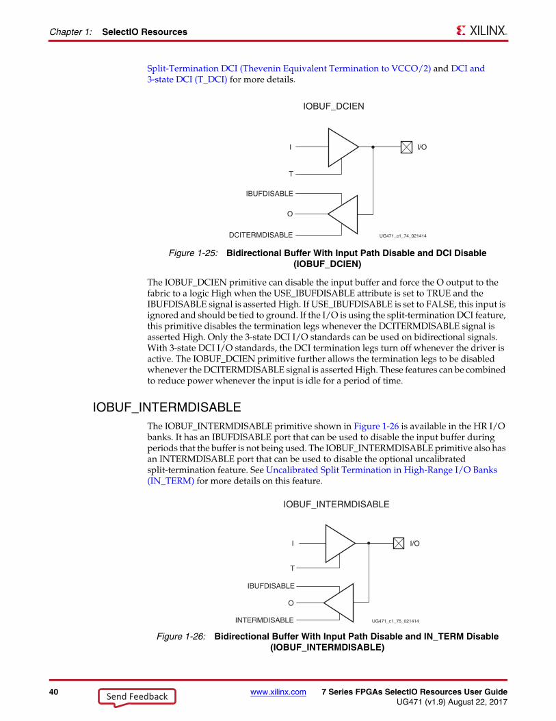
40 www.xilinx.com 7 Series FPGAs SelectIO Resources User GuideUG471 (v1.9) August 22, 2017
Chapter 1: SelectIO Resources
Split-Termination DCI (Thevenin Equivalent Termination to VCCO/2) and DCI and 3-state DCI (T_DCI) for more details.
The IOBUF_DCIEN primitive can disable the input buffer and force the O output to the fabric to a logic High when the USE_IBUFDISABLE attribute is set to TRUE and the IBUFDISABLE signal is asserted High. If USE_IBUFDISABLE is set to FALSE, this input is ignored and should be tied to ground. If the I/O is using the split-termination DCI feature, this primitive disables the termination legs whenever the DCITERMDISABLE signal is asserted High. Only the 3-state DCI I/O standards can be used on bidirectional signals. With 3-state DCI I/O standards, the DCI termination legs turn off whenever the driver is active. The IOBUF_DCIEN primitive further allows the termination legs to be disabled whenever the DCITERMDISABLE signal is asserted High. These features can be combined to reduce power whenever the input is idle for a period of time.
IOBUF_INTERMDISABLEThe IOBUF_INTERMDISABLE primitive shown in Figure 1-26 is available in the HR I/O banks. It has an IBUFDISABLE port that can be used to disable the input buffer during periods that the buffer is not being used. The IOBUF_INTERMDISABLE primitive also has an INTERMDISABLE port that can be used to disable the optional uncalibrated split-termination feature. See Uncalibrated Split Termination in High-Range I/O Banks (IN_TERM) for more details on this feature.
X-Ref Target - Figure 1-25
Figure 1-25: Bidirectional Buffer With Input Path Disable and DCI Disable (IOBUF_DCIEN)
IOBUF_DCIEN
I/OI
UG471_c1_74_021414
O
DCITERMDISABLE
IBUFDISABLE
T
X-Ref Target - Figure 1-26
Figure 1-26: Bidirectional Buffer With Input Path Disable and IN_TERM Disable (IOBUF_INTERMDISABLE)
UG471_c1_75_021414
IOBUF_INTERMDISABLE
I/OI
O
INTERMDISABLE
IBUFDISABLE
T
Send Feedback

7 Series FPGAs SelectIO Resources User Guide www.xilinx.com 41UG471 (v1.9) August 22, 2017
7 Series FPGA SelectIO Primitives
The IOBUF_INTERMDISABLE primitive can disable the input buffer and force the O output to the fabric to a logic High when the USE_IBUFDISABLE attribute is set to TRUE and the IBUFDISABLE signal is asserted High. If USE_IBUFDISABLE is set to FALSE, this input is ignored and should be tied to ground. If the I/O is using the optional uncalibrated split-termination feature (IN_TERM), those termination legs are disabled whenever the driver is active (T is low). This primitive further allows the termination legs to be disabled whenever the INTERMDISABLE signal is asserted High. These features can be combined to reduce power whenever the input is idle for a period of time.
IOBUFDSFigure 1-27 shows the differential input/output buffer primitive. A logic High on the T pin disables the output buffer.
IOBUFDS_DCIENThe IOBUFDS_DCIEN primitive shown in Figure 1-28 is available in the HP I/O banks. It has a IBUFDISABLE port that can be used to disable the input buffer during periods that the buffer is not being used. The IOBUFDS_DCIEN primitive also has a DCITERMDISABLE port that can be used to manually disable the optional DCI split-termination feature. See Split-Termination DCI (Thevenin Equivalent Termination to VCCO/2) and DCI and 3-state DCI (T_DCI) for more details.
X-Ref Target - Figure 1-27
Figure 1-27: Differential Input/Output Buffer Primitive (IOBUFDS)
ug471_c1_24_041112
IOBUFDS
I/O to/fromdevice pad
I (Input)from FPGA
O (Output)to FPGA
T3-state Input
+
–
+
–
IO
IOB
Send Feedback

42 www.xilinx.com 7 Series FPGAs SelectIO Resources User GuideUG471 (v1.9) August 22, 2017
Chapter 1: SelectIO Resources
The IOBUFDS_DCIEN primitive can disable the input buffer and force the O output to the fabric to a logic High when the USE_IBUFDISABLE attribute is set to TRUE and the IBUFDISABLE signal is asserted High. If USE_IBUFDISABLE is set to FALSE, this input is ignored and should be tied to ground. If the I/O is using the split-termination DCI feature, this primitive disables the termination legs whenever the DCITERMDISABLE signal is asserted High. Only the 3-state DCI I/O standards can be used on bidirectional signals. With 3-state DCI I/O standards, the DCI termination legs turn off whenever the driver is active. The IOBUFDS_DCIEN primitive further allows the termination legs to be disabled whenever the DCITERMDISABLE signal is asserted High. These features can be combined to reduce power whenever the input is idle for a period of time.
IOBUFDS_DIFF_OUTFigure 1-29 shows the differential input/output buffer primitive with complementary outputs (O and OB). This primitive is only recommended for use by experienced Xilinx designers with memory interface applications. A logic High on the T pin disables the output buffer.
X-Ref Target - Figure 1-28
Figure 1-28: Differential Bidirectional Buffer With Input Path Disable and DCI Disable (IOBUFDS_DCIEN)
IOBUFDS_DCIEN
IBUFDISABLE
DCITERMDISABLE
T
I
O
IO
IOB
UG471_c1_69_021214
Send Feedback

7 Series FPGAs SelectIO Resources User Guide www.xilinx.com 43UG471 (v1.9) August 22, 2017
7 Series FPGA SelectIO Primitives
IOBUFDS_DIFF_OUT_DCIENThe IOBUFDS_DIFF_OUT_DCIEN primitive shown in Figure 1-30 is available in the HP I/O banks. It has complementary differential outputs, an IBUFDISABLE port that can be used to disable the input buffer during periods that the buffer is not being used, and a DCITERMDISABLE port that can be used to manually disable the optional DCI split-termination feature. See Split-Termination DCI (Thevenin Equivalent Termination to VCCO/2) and DCI and 3-state DCI (T_DCI) for more details.
The IOBUFDS_DIFF_OUT_DCIEN primitive can disable the input buffer and force both the O and OB outputs to the fabric High when the USE_IBUFDISABLE attribute is set to TRUE and the IBUFDISABLE signal is asserted High. If USE_IBUFDISABLE is set to FALSE, this input is ignored and should be tied to ground. If the I/O is using the
X-Ref Target - Figure 1-29
Figure 1-29: Differential Input/Output Buffer Primitive With Complementary Outputs for the Input Buffer (IOBUFDS_DIFF_OUT)
ug471_c1_26_041112
IOBUFDS_DIFF_OUT
To/From Device Pad
IO
IOB
Input from FPGA
Output to FPGA
3-state input frommaster OLOGIC
O
OB
TM
I
3-state input fromslave OLOGIC
TS
X-Ref Target - Figure 1-30
Figure 1-30: Differential Bidirectional Buffer with Complementary Outputs, Input Path Disable, and DCI Disable (IOBUFDS_DCIEN)
IOBUFDS_DIFF_OUT_DCIEN
IBUFDISABLE
DCITERMDISABLE
TSI
TM
O
OB
IO
IOB
UG471_c1_70_021214
Send Feedback

44 www.xilinx.com 7 Series FPGAs SelectIO Resources User GuideUG471 (v1.9) August 22, 2017
Chapter 1: SelectIO Resources
split-termination DCI feature, this primitive disables the termination legs whenever the DCITERMDISABLE signal is asserted high. Only the 3-state DCI I/O standards can be used on bidirectional signals. With 3-state DCI I/O standards, the DCI termination legs turn off whenever the driver is active (TS is low for the IO output, TM is low for the IOB output). The IOBUFDS_DIFF_OUT_DCIEN primitive further allows the termination legs to be disabled whenever the DCITERMDISABLE signal is asserted High. These features can be combined to reduce power whenever the input is idle for a period of time.
IOBUFDS_DIFF_OUT_INTERMDISABLEThe IOBUFDS_DIFF_OUT_INTERMDISABLE primitive shown in Figure 1-31 is available in the HR I/O banks. It has an IBUFDISABLE port that can be used to disable the input buffer during periods that the buffer is not being used. The IOBUFDS_DIFF_OUT_INTERMDISABLE primitive also has an INTERMDISABLE port that can be used to disable the optional uncalibrated split-termination feature. See Uncalibrated Split Termination in High-Range I/O Banks (IN_TERM) for more details on this feature.
The IOBUFDS_DIFF_OUT_INTERMDISABLE primitive can disable the input buffer and force both the O and OB outputs to the fabric High when the USE_IBUFDISABLE attribute is set to TRUE and the IBUFDISABLE signal is asserted High. If USE_IBUFDISABLE is set to FALSE, this input is ignored and should be tied to ground. If the I/O is using the optional uncalibrated split-termination feature (IN_TERM), those termination legs are also disabled whenever the driver is active (TS is low for the IO output, TM is low for the IOB output). The IOBUFDS_DIFF_OUT_INTERMDISABLE primitive further allows the termination legs to be disabled whenever the INTERMDISABLE signal is asserted High. These features can be combined to reduce power whenever the input is idle for a period of time.
IOBUFDS_INTERMDISABLEThe IOBUFDS_INTERMDISABLE primitive shown in Figure 1-32 is available in the HR I/O banks. It has an IBUFDISABLE port that can be used to disable the input buffer during periods that the buffer is not being used. The IOBUFDS_INTERMDISABLE primitive also has an INTERMDISABLE port that can be used to disable the optional uncalibrated
X-Ref Target - Figure 1-31
Figure 1-31: Differential Bidirectional Buffer with Complementary Outputs, Input Buffer Disable, and IN_TERM Disable (IOBUFDS_DIFF_OUT_INTERMDISABLE)
IOBUFDS_DIFF_OUT_INTERMDISABLE
IBUFDISABLE
INTERMDISABLE
TSI
TM
O
OB
IO
IOB
UG471_c1_71_021412
Send Feedback

7 Series FPGAs SelectIO Resources User Guide www.xilinx.com 45UG471 (v1.9) August 22, 2017
7 Series FPGA SelectIO Primitives
split-termination feature. See Uncalibrated Split Termination in High-Range I/O Banks (IN_TERM) for more details on this feature.
The IOBUFDS_INTERMDISABLE primitive can disable the input buffer and force the O output to the fabric to a logic High when the USE_IBUFDISABLE attribute is set to TRUE and the IBUFDISABLE signal is asserted High. If USE_IBUFDISABLE is set to FALSE, this input is ignored and should be tied to ground. If the I/O is using the optional uncalibrated split-termination feature (IN_TERM), those termination legs are disabled whenever the driver is active (T is low). This primitive further allows the termination legs to be disabled whenever the INTERMDISABLE signal is asserted High. These features can be combined to reduce power whenever the input is idle for a period of time.
OBUFAn output buffer (OBUF) must be used to drive signals from 7 series devices to external output pads. A generic 7 series FPGA OBUF primitive is shown in Figure 1-33.
OBUFDSFigure 1-34 shows the differential output buffer primitive.
X-Ref Target - Figure 1-32
Figure 1-32: Differential Bidirectional Buffer With Input Buffer Disable and IN_TERM Disable (IOBUFDS_INTERMDISABLE)
IOBUFDS_INTERMDISABLE
IBUFDISABLE
INTERMDISABLE
T
I
O
IO
IOB
UG471_c1_68_021214
X-Ref Target - Figure 1-33
Figure 1-33: Output Buffer Primitive (OBUF)
ug471_c1_18_011811
OBUF
O (Output)to device pad
I (Input)From FPGA
Send Feedback

46 www.xilinx.com 7 Series FPGAs SelectIO Resources User GuideUG471 (v1.9) August 22, 2017
Chapter 1: SelectIO Resources
OBUFTThe generic 3-state output buffer OBUFT, shown in Figure 1-35, typically implements 3-state outputs or bidirectional I/O.
OBUFTDSFigure 1-36 shows the differential 3-state output buffer primitive.
7 Series FPGA SelectIO Attributes/ConstraintsAccess to some 7 series FPGA I/O resource features (e.g., location constraints, input delay, output drive strength, and slew rate) is available through the attributes/constraints associated with these features. For more information about implementing these constraints and attributes as well as others, see UG625: Constraints Guide (for the ISE tools) or UG912: Vivado Design Suite Properties Reference Guide.
DCI_CASCADE ConstraintThe DCI_CASCADE constraint identifies a DCI master bank and its corresponding slave banks. See DCI Cascading, page 22 for more information.
X-Ref Target - Figure 1-34
Figure 1-34: Differential Output Buffer Primitive (OBUFDS)
ug471_c1_22_041112
+
– OB
OI
OBUFDS
Input from FPGA
Output toDevice Pads
X-Ref Target - Figure 1-35
Figure 1-35: 3-State Output Buffer Primitive (OBUFT)
ug471_c1_19_011811
OBUFT
O (Output)to device pad
I (Input)From FPGA
T3-state input
X-Ref Target - Figure 1-36
Figure 1-36: Differential 3-state Output Buffer Primitive (OBUFTDS)
ug471_c1_23_041112
+
– OB
OI
T
OBUFTDS
Input from FPGA
3-state Input
Output toDevice Pads
Send Feedback

7 Series FPGAs SelectIO Resources User Guide www.xilinx.com 47UG471 (v1.9) August 22, 2017
7 Series FPGA SelectIO Attributes/Constraints
The DCI_CASCADE attribute uses this syntax in the UCF file:
CONFIG DCI_CASCADE = "<master> <slave1> <slave2> ...";
For example:
CONFIG DCI_CASCADE = "11 13 15 17";
Location ConstraintsThe location constraint (LOC) must be used to specify the I/O location of an instantiated I/O primitive. The possible values for the location constraint are all the external port identifiers (e.g., A8, M5, AM6, etc.). These values are device and package size dependent.
The LOC attribute uses the following syntax in the UCF file:
INST <I/O_BUFFER_INSTANTIATION_NAME> LOC = "<EXTERNAL_PORT_IDENTIFIER>";
Example:
INST MY_IO LOC=R7;
IOSTANDARD AttributeThe IOSTANDARD attribute is available to choose the values for an I/O standard for all I/O buffers. The supported I/O standards are listed in the specific 7 series FPGAs data sheets, however, Table 1-56 lists the IOSTANDARD support by bank type (HR, HP, or both). The IOSTANDARD attribute uses the following syntax in the UCF file:
INST <I/O_BUFFER_INSTANTIATION_NAME> IOSTANDARD=”<IOSTANDARD VALUE>”;
The IOSTANDARD default for single-ended I/O is LVCMOS18, for differential I/Os the default is DIFF_HSTL_II_18.
IBUF_LOW_PWR AttributeThe IBUF_LOW_PWR attribute is available for the following inputs:
• All I/O standards with differential inputs, including:
• LVDS
• LVDS_25
• PPDS_25
• RSDS_25
• MINI_LVDS_25
• BLVDS_25
• DIFF_HSTL (all variations)
• DIFF_SSTL (all variations)
• DIFF_MOBILE_DDR
• DIFF_HSUL (all variations)
Send Feedback

48 www.xilinx.com 7 Series FPGAs SelectIO Resources User GuideUG471 (v1.9) August 22, 2017
Chapter 1: SelectIO Resources
• All VREF-based inputs such as HSLVDCI, SSTL, HSTL, and HSUL
• All input and bidirectional primitives
The IBUF_LOW_PWR attribute allows an optional trade-off between performance and power. The change in the performance is reflected in the delay through the input buffer and can be measured in the static timing report for the design. The change in power can be estimated using the XPower Estimator (XPE) or XPower Analyzer (XPA) tools.
This attribute is set to TRUE by default, which implements the input buffer in the lower-power mode rather than the higher-performance mode. The IBUF_LOW_PWR attribute is applied to the I/O buffer instance and uses the following syntax in the UCF file:
INST <I/O_BUFFER_INSTANTIATION_NAME> IBUF_LOW_PWR=[TRUE|FALSE];
Output Slew Rate AttributesA variety of attribute values provide the option of choosing the desired slew rate for I/O output buffers. For LVCMOS, LVTTL, SSTL, HSTL, MOBILE_DDR, and HSUL output buffers, including the differential versions, the desired slew rate can be specified with the SLEW attribute.
It might be important to specify FAST slew rate for high-performance applications such as high-frequency memory interfaces. However, faster slew rates can also lead to reflections or increased noise issues if not properly designed (such as with terminations, transmission line impedance continuity, and cross-coupling).
The allowed values for the SLEW attribute are:
• SLEW = SLOW (Default)
• SLEW = FAST
The SLEW attribute uses the following syntax in the UCF file:
INST <I/O_BUFFER_INSTANTIATION_NAME> SLEW = "<SLEW_VALUE>";
By default, the slew rate for each output buffer is set to SLOW. This is the default used to minimize the power bus transients when switching non-critical signals.
Output Drive Strength AttributesFor LVCMOS and LVTTL output buffers (OBUF, OBUFT, and IOBUF), the desired drive strength (in mA) can be specified with the DRIVE attribute.
The allowed values for the DRIVE attribute are shown in Table 1-8. The default DRIVE value is 12.
Table 1-8: Allowed Values for the DRIVE Attribute
Standard HR Bank Current Drive (mA) HP Bank Current Drive (mA)
LVCMOS12 4, 8, or 12 2, 4, 6, or 8
LVCMOS15 4, 8, 12, or 16 2, 4, 6, 8, 12, or 16
LVCMOS18 4, 8, 12, 16, or 24 2, 4, 6, 8, 12, or 16
LVCMOS25 4, 8, 12, or 16 N/A
LVCMOS33 4, 8, 12, or 16 N/A
LVTTL 4, 8, 12, 16, or 24 N/A
Send Feedback

7 Series FPGAs SelectIO Resources User Guide www.xilinx.com 49UG471 (v1.9) August 22, 2017
7 Series FPGA SelectIO Attributes/Constraints
The DRIVE attribute uses the following syntax in the UCF file:
INST <I/O_BUFFER_INSTANTIATION_NAME> DRIVE = "<DRIVE_VALUE>";
PULLUP/PULLDOWN/KEEPER Attribute for IBUF, OBUFT, and IOBUFInput buffers (e.g., IBUF), 3-state output (e.g., OBUFT), and bidirectional (e.g., IOBUF) buffers can have a weak pull-up resistor, a weak pull-down resistor, or a weak “keeper” circuit. This feature can be invoked by adding the following possible constraint values to the relevant net of the buffers:
• PULLUP
• PULLDOWN
• KEEPER
The logic level can be set globally for unused I/O using the BITSTREAM.CONFIG.UNUSEDPIN property. For more information on implementing these attributes on either individual I/Os or globally for all I/Os, see the pull-up, pull-down, and keeper descriptions in UG625: Constraints Guide (for the ISE tools) or UG912: Vivado Design Suite Properties Reference Guide. For more information on implementing device configuration bitstream settings, refer to UG628: Command Line Tools User Guide (for the ISE tools) or UG908: Vivado Design Suite User Guide: Programming and Debugging.
Differential Termination AttributeThe differential termination (DIFF_TERM) attribute supports the differential I/O standards when used as inputs. It is used to turn the built-in, 100Ω, differential termination on or off. The on-chip input differential termination in 7 series devices provides major advantages over using a discrete resistor by removing the stub at the receiver completely and therefore greatly improving signal integrity. Additionally it:
• Consumes less power than DCI termination
• Does not use VRP/VRN pins (DCI)
This attribute can be applied to input pins for the following I/O standards:
• LVDS
• LVDS_25
• MINI_LVDS_25
• PPDS_25
• RSDS_25
The VCCO of the I/O bank must be connected to 1.8V for LVDS, and 2.5V for the other differential I/O standards to provide 100Ω of effective differential termination. DIFF_TERM is only available for inputs and can only be used the appropriate VCCO voltage.
The DIFF_TERM attribute can be specified in the UCF constraints file or by setting the appropriate value in the generic map (VHDL) or in-line parameter (Verilog) of the instantiated IBUFDS, IBUFGDS, IBUFDS_DIFF_OUT, or IOBUFDS_DIFF_OUT primitives. Refer to the ISE tools language templates or the 7 series FPGA HDL Libraries Guide for the proper syntax for instantiating these primitives and setting the DIFF_TERM attribute.
The allowed values for the DIFF_TERM attribute are:
• DIFF_TERM = TRUE
Send Feedback

50 www.xilinx.com 7 Series FPGAs SelectIO Resources User GuideUG471 (v1.9) August 22, 2017
Chapter 1: SelectIO Resources
• DIFF_TERM = FALSE (Default)
The DIFF_TERM attribute uses the following syntax in the UCF file:
INST <I/O_BUFFER_INSTANTIATION_NAME> DIFF_TERM = "[TRUE|FALSE]";
Internal VREF
The VREF for an I/O bank can be (optionally) generated inside the 7 series FPGA. Internal generation removes the need to provide for a particular VREF supply rail on the printed circuit board (PCB) and frees the multi-purpose VREF pins in a given I/O bank to be used as normal I/O pins. Consider this alternative when the 7 series FPGA is the only device on the board/system requiring a particular VREF voltage supply level, or if there is a shortage of I/O pins in a given I/O bank. The internally generated VREF (INTERNAL_VREF) is sourced from the VCCAUX. Each bank has a single VREF plane and each I/O bank can therefore only have the optional INTERNAL_VREF set to a single voltage level for the entire bank.
The constraint INTERNAL_VREF is assigned to one bank at time.
Example 1: INTERNAL_VREF for Bank 14 using HSTL_II (1.5V), which requires a 0.75V reference voltage, uses the following constraint:
INTERNAL_VREF_BANK14 = 0.75;
Example 2: INTERNAL_VREF for Bank 15 using HSTL_II_18 (1.8V), which requires a 0.9V reference voltage, uses the following constraint.
INTERNAL_VREF_BANK15 = 0.90;
The rules for using INTERNAL_VREF are:
• One value of VREF can be set for the bank.
• INTERNAL_VREF can only be set to the nominal reference voltage value of a given I/O standard.
• Valid settings of INTERNAL_VREF are:
• 0.60• 0.675• 0.75• 0.90
• When using INTERNAL_VREF in a bank, the multi-purpose VREF pins in that bank can be used as normal I/O.
The rules for combining I/O standards in the same bank also apply for INTERNAL_VREF.
VCCAUX_IO ConstraintVCCAUX_IO is a constraint available for I/O nets and primitives that should be specified in the design if the VCCAUX_IO pins for any HP banks are going to be set to 2.0V. VCCAUX_IO defaults to a value of DONTCARE but can be set to NORMAL (1.8V) or HIGH (2.0V). If the VCCAUX_IO pins in a given bank are to be powered at 2.0V, at least one I/O net or primitive in that bank should have its VCCAUX_IO constraint set to HIGH, and all other I/O nets and primitives that must either be set to HIGH or DONTCARE. If the VCCAUX_IO pins in a bank are to be powered at 1.8V, at least one I/O net or primitive in that bank should have this constraint set to NORMAL, and all other I/O nets or primitives should be set to either NORMAL or DONTCARE.
Send Feedback

7 Series FPGAs SelectIO Resources User Guide www.xilinx.com 51UG471 (v1.9) August 22, 2017
Supported I/O Standards and Terminations
In VHDL, the VHDL constraint associated with the IOB primitive instantiation is declared as follows:
attribute VCCAUX_IO of {component_name |label_name}:{component|label} is “{NORMAL|HIGH|DONTCARE}”;
In Verilog, the Verilog constraint is placed immediately before the module or instantiation of the IOB primitive. The Verilog constraint is specified as follows:
(* VCCAUX_IO = {NORMAL|HIGH|DONTCARE}*)UCF and NCF SyntaxNET “net_name” VCCAUX_IO=(0|NORMAL|HIGH|DONTCARE);INST “instance_name ” VCCAUX_IO=(NORMAL|HIGH|DONTCARE);
7 Series FPGA I/O Resource VHDL/Verilog ExamplesThe VHDL and Verilog example syntaxes for instantiating 7 series FPGA I/O resources are found in UG768: Xilinx 7 Series FPGA Libraries Guide for HDL Designs.
Supported I/O Standards and TerminationsThe following sections provide an overview of the I/O standards and options supported by all 7 series devices.
While most 7 series FPGA I/O supported standards specify a range of allowed voltages, this chapter records typical voltage values only. Detailed information on each specification can be found on the Electronic Industry Alliance JEDEC web site at http://www.jedec.org.
LVTTL (Low Voltage TTL)
LVTTL is a general-purpose EIA/JESD standard for 3.3V applications that uses a single-ended CMOS input buffer and a push-pull output buffer. This standard requires a 3.3V output source voltage (VCCO), but does not require the use of a reference voltage (VREF) or a termination voltage (VTT). This standard is defined by JEDEC (JESD 8C.01).
Sample circuits illustrating both unidirectional and bidirectional LVTTL termination techniques are shown in Figure 1-37 and Figure 1-38. These two diagrams show examples of source-series and parallel terminated topologies.
Table 1-9: Available I/O Bank Type
HR HP
Available N/A
Send Feedback

52 www.xilinx.com 7 Series FPGAs SelectIO Resources User GuideUG471 (v1.9) August 22, 2017
Chapter 1: SelectIO Resources
Figure 1-37 shows unidirectional terminated topologies.X-Ref Target - Figure 1-37
Figure 1-37: LVTTL Unidirectional Termination
Z0
IOB IOB
LVTTL LVTTL
Z0
IOB IOB
LVTTL LVTTL
Z0
IOB IOB
LVTTL LVTTL
ug471_c1_27_011811
VTT
Note: VTT is any voltage from 0V to VCCO
RP = Z0
RS = Z0 – RD
Send Feedback

7 Series FPGAs SelectIO Resources User Guide www.xilinx.com 53UG471 (v1.9) August 22, 2017
Supported I/O Standards and Terminations
Figure 1-38 shows a bidirectional, parallel-terminated topology.
Table 1-10 details the allowed attributes that can be applied to the LVTTL I/O standard. This standard is only available in the HR I/O banks.
X-Ref Target - Figure 1-38
Figure 1-38: LVTTL Bidirectional Termination
Table 1-10: Allowed Attributes for the LVTTL I/O Standards
AttributesPrimitives
IBUF/IBUFG OBUF/OBUFT/ IOBUF
IOSTANDARD LVTTL LVTTL
DRIVE N/A 4, 8, 12 (default), 16, 24
SLEW N/A {FAST, SLOW}
Z0
IOB IOB
LVTTL
Z0
IOB IOB
LVTTL LVTTL
VTT
Note: VTT is any voltage from 0V to VCCO
RP = Z0
VTT
RP = Z0
ug471_c1_28_011811
LVTTL
Send Feedback

54 www.xilinx.com 7 Series FPGAs SelectIO Resources User GuideUG471 (v1.9) August 22, 2017
Chapter 1: SelectIO Resources
LVCMOS (Low Voltage CMOS)
LVCMOS is a widely used switching standard implemented in CMOS transistors. This standard is defined by JEDEC (JESD 8C.01). The LVCMOS standards supported in 7 series FPGAs are: LVCMOS12, LVCMOS15, LVCMOS18, LVCMOS25, and LVCMOS33.
Sample circuits illustrating both unidirectional and bidirectional LVCMOS termination techniques are shown in Figure 1-39 and Figure 1-40. These two diagrams show examples of source-series and parallel terminated topologies.
Figure 1-39 shows unidirectional terminated topologies.
Table 1-11: Available I/O Bank Type
HR HP
Available Available
X-Ref Target - Figure 1-39
Figure 1-39: LVCMOS Unidirectional Termination
Z0
IOB IOB
LVCMOS LVCMOS
Z0
IOB IOB
LVCMOS LVCMOS
Z0
IOB IOB
LVCMOS LVCMOS
ug471_c1_29_011811
VTT
Note: VTT is any voltage from 0V to VCCO
RP = Z0
RS = Z0 – RD
Send Feedback

7 Series FPGAs SelectIO Resources User Guide www.xilinx.com 55UG471 (v1.9) August 22, 2017
Supported I/O Standards and Terminations
Figure 1-40 shows a bidirectional, parallel-terminated topology.
Table 1-12 details the allowed attributes that can be applied to the LVCMOS33 and LVCMOS25 I/O standards. These standards are only available in the HR I/O banks.
Table 1-13 details the allowed attributes that can be applied to the LVCMOS18 I/O standard. This standard is available in both the HR and HP I/O banks.
X-Ref Target - Figure 1-40
Figure 1-40: LVCMOS Bidirectional Termination
Table 1-12: Allowed Attributes for the LVCMOS33 and LVCMOS25 I/O Standards
AttributesPrimitives
IBUF/IBUFG OBUF/OBUFT/ IOBUF
IOSTANDARD LVCMOS33, LVCMOS25 LVCMOS33, LVCMOS25
DRIVE N/A 4, 8, 12, 16
SLEW N/A {FAST, SLOW}
Table 1-13: Allowed Attributes for the LVCMOS18 I/O Standard
Attributes
Primitives
IBUF/IBUFGOBUF/OBUFT/IOBUF
HP I/O Banks HR I/O Banks
IOSTANDARD LVCMOS18 LVCMOS18 LVCMOS18
DRIVE N/A 2, 4, 6, 8, 12, 16 4, 8, 12, 16, 24
SLEW N/A {FAST, SLOW} {FAST, SLOW}
Z0
IOB IOB
LVCMOS
Z0
IOB IOB
LVCMOS LVCMOS
VTT
Note: VTT is any voltage from 0V to VCCO
RP = Z0
VTT
RP = Z0
ug471_c1_30_011811
LVCMOS
Send Feedback

56 www.xilinx.com 7 Series FPGAs SelectIO Resources User GuideUG471 (v1.9) August 22, 2017
Chapter 1: SelectIO Resources
Table 1-14 details the allowed attributes that can be applied to the LVCMOS15 I/O standard. This standard is available in both the HR and HP I/O banks.
Table 1-15 details the allowed attributes that can be applied to the LVCMOS12 I/O standard. This standard is available in both the HR and HP I/O banks.
LVDCI (Low-Voltage Digitally Controlled Impedance)
Using these I/O buffers configures the outputs as controlled impedance drivers. The receiver of LVDCI is identical to a LVCMOS receiver. Some I/O standards, such as LVCMOS, must have a drive impedance that matches the characteristic impedance of the driven line. The HP I/O banks in the 7 series devices provide a controlled impedance output driver to provide series termination without external-source termination resistors. The impedance is set by the common external reference resistors, with resistance equal to the trace characteristic impedance, Z0.
Sample circuits illustrating both unidirectional and bidirectional topologies for a controlled impedance driver are shown in Figure 1-41 and Figure 1-42. The DCI I/O standards supporting a controlled impedance driver are: LVDCI_15 and LVDCI_18.
Table 1-14: Allowed Attributes for the LVCMOS15 I/O Standard
Attributes
Primitives
IBUF/IBUFGOBUF/OBUFT/IOBUF
HP I/O Banks HR I/O Banks
IOSTANDARD LVCMOS15 LVCMOS15 LVCMOS15
DRIVE N/A 2, 4, 6, 8, 12, 16 4, 8, 12, 16
SLEW N/A {FAST, SLOW} {FAST, SLOW}
Table 1-15: Allowed Attributes for the LVCMOS12 I/O Standard
Attributes
Primitives
IBUF/IBUFGOBUF/OBUFT/IOBUF
HP I/O Banks HR I/O Banks
IOSTANDARD LVCMOS12 LVCMOS12 LVCMOS12
DRIVE N/A 2, 4, 6, 8 4, 8, 12
SLEW N/A {FAST, SLOW} {FAST, SLOW}
Table 1-16: Available I/O Bank Type
HR HP
N/A Available
Send Feedback

7 Series FPGAs SelectIO Resources User Guide www.xilinx.com 57UG471 (v1.9) August 22, 2017
Supported I/O Standards and Terminations
LVDCI_DV2
A controlled impedance driver with half impedance (source termination) can also provide drivers with one half of the impedance of the reference resistors. This allows reference resistors to be twice as large, thus reducing static power consumption through VRN/VRP. The I/O standards supporting a controlled impedance driver with half impedance are: LVDCI_DV2_15 and LVDCI_DV2_18. Figure 1-43 and Figure 1-44 illustrate a controlled driver with half impedance unidirectional topologies.
To match the drive impedance to Z0 when using a driver with half impedance, the reference resistor R must be twice Z0.
X-Ref Target - Figure 1-41
Figure 1-41: Unidirectional Controlled Impedance Driver Topology
X-Ref Target - Figure 1-42
Figure 1-42: Bidirectional Controlled Impedance Driver Topology
Z0
IOB IOB
LVDCI LVDCI
ug471_c1_31_011811
R0 = RVRN = RVRP = Z0
Z0
IOB IOB
LVDCI LVDCI
ug471_c1_32_011811
R0 = RVRN = RVRP = Z0
R0 = RVRN = RVRP = Z0
Table 1-17: Available I/O Bank Type
HR HP
N/A Available
Send Feedback

58 www.xilinx.com 7 Series FPGAs SelectIO Resources User GuideUG471 (v1.9) August 22, 2017
Chapter 1: SelectIO Resources
There are no optional current drive strength settings for LVDCI drivers. When the driver impedance is one-half of the VRN/VRP reference resistors, it is indicated by the addition of DV2 to the attribute name.
X-Ref Target - Figure 1-43
Figure 1-43: Unidirectional Controlled Impedance Driver with Half Impedance Topology
X-Ref Target - Figure 1-44
Figure 1-44: Bidirectional Controlled Impedance Driver with Half Impedance Topology
Z0
IOB IOB
LVDCI_DV2 LVDCI_DV2
ug471_c1_33_011811
R0 = ½RVRN = ½RVRP = Z0
Z0
IOB IOB
LVDCI_DV2 LVDCI_DV2
ug471_c1_34_011811
R0 = ½RVRN = ½RVRP = Z0
R0 = ½RVRN = ½RVRP = Z0
Send Feedback

7 Series FPGAs SelectIO Resources User Guide www.xilinx.com 59UG471 (v1.9) August 22, 2017
Supported I/O Standards and Terminations
HSLVDCI (High-Speed LVDCI)
The HSLVDCI standard is intended for bidirectional use. The driver is identical to LVDCI, while the input is identical to HSTL and SSTL. By using a VREF-referenced input, HSLVDCI allows greater input sensitivity at the receiver than when using a single-ended LVCMOS-type receiver.
A sample circuit illustrating bidirectional termination techniques for an HSLVDCI controlled impedance driver is shown in Figure 1-45. The DCI I/O standards supporting a controlled impedance driver with a VREF referenced input are: HSLVDCI_15 and HSLVDCI_18.
For electrical specifications, refer to the LVDCI VOH and VOL entries in the 7 series data sheets.
Table 1-18: Available I/O Bank Type
HR HP
N/A Available
X-Ref Target - Figure 1-45
Figure 1-45: HSLVDCI Controlled Impedance Driver with Bidirectional Termination
Z0
IOBHSLVDCI_15HSLVDCI_18
HSLVDCI_15HSLVDCI_18
ug471_c1_35_121610
R0 = RVRN = RVRP = Z0
R0 = RVRN = RVRP = Z0
IOB
VREF = VCCO/2
VREF = VCCO/2
+
–
Send Feedback

60 www.xilinx.com 7 Series FPGAs SelectIO Resources User GuideUG471 (v1.9) August 22, 2017
Chapter 1: SelectIO Resources
HSTL (High-Speed Transceiver Logic)The high-speed transceiver logic (HSTL) standard is a general purpose high-speed bus standard is defined by JEDEC (JESD8-6). The HSTL standards have four variations (classes). To support clocking high-speed memory interfaces, differential versions are also available. 7 series FPGA I/O supports class-I for the 1.2V version of HSTL (in HP banks), and class-I and II for the 1.5V and 1.8V versions, including the differential versions. The differential versions of the standard require a differential amplifier input buffer and a push-pull output buffer. The HP I/O banks also support DCI versions.
HSTL_ I and HSTL_ I_18
HSTL_I and HSTL_ I_18 use VCCO/2 as a parallel-termination voltage (VTT) and are intended for use in unidirectional links.
HSTL_I_12
HSTL_I_12 uses VCCO/2 as a parallel-termination voltage (VTT) and is intended for use in unidirectional links.
HSTL_ I_DCI and HSTL_ I_DCI_18
HSTL_I_DCI and HSTL_I_DCI_18 provide on-chip split thevenin termination powered from VCCO, creating an equivalent parallel-termination voltage (VTT) of VCCO/2, and are intended for use in unidirectional links.
HSTL_ II and HSTL_ II_18
HSTL_II and HSTL_II_18 use VCCO/2 as a parallel-termination voltage (VTT) and are intended for use in bidirectional links.
Table 1-19: Available I/O Bank Type
HR HP
Available Available
Table 1-20: Available I/O Bank Type
HR HP
N/A Available
Table 1-21: Available I/O Bank Type
HR HP
N/A Available
Table 1-22: Available I/O Bank Type
HR HP
Available Available
Send Feedback

7 Series FPGAs SelectIO Resources User Guide www.xilinx.com 61UG471 (v1.9) August 22, 2017
Supported I/O Standards and Terminations
HSTL_ II_DCI and HSTL_ II_DCI_18
HSTL_II_DCI and HSTL_II_DCI_18 provide on-chip split thevenin termination powered from VCCO, creating an equivalent termination voltage of VCCO/2, and are intended for use in bidirectional links.
HSTL_ II_T_DCI and HSTL_ II_T_DCI_18
HSTL_ II_T_DCI and HSTL_ II_T_DCI_18 provide on-chip split-thevenin termination powered from VCCO that creates an equivalent termination voltage of VCCO/2 at the receiver when the driver is 3-stated. When the driver is not 3-stated, these two standards do not have termination.
DIFF_HSTL_I and DIFF_HSTL_I_18
Differential HSTL class-I pairs complementary single-ended HSTL_I type drivers with a differential receiver, and are intended to be used in unidirectional links.
DIFF_HSTL_I_DCI and DIFF_HSTL_I_DCI_18
Differential HSTL class-I pairs complementary single-ended HSTL_I type drivers with a differential receiver, including on-chip split-thevenin termination, and are intended to be used in unidirectional links.
DIFF_HSTL_ II and DIFF_HSTL_II_18
Differential HSTL class-II pairs complementary single-ended HSTL_II type drivers with a differential receiver. Differential HSTL class-II is intended to be used in bidirectional links.
Table 1-23: Available I/O Bank Type
HR HP
N/A Available
Table 1-24: Available I/O Bank Type
HR HP
N/A Available
Table 1-25: Available I/O Bank Type
HR HP
Available Available
Table 1-26: Available I/O Bank Type
HR HP
N/A Available
Table 1-27: Available I/O Bank Type
HR HP
Available Available
Send Feedback

62 www.xilinx.com 7 Series FPGAs SelectIO Resources User GuideUG471 (v1.9) August 22, 2017
Chapter 1: SelectIO Resources
Differential HSTL can also be used for differential clock and DQS signals in memory interface designs.
DIFF_HSTL_II_DCI and DIFF_HSTL_II_DCI_18
Differential HSTL class-II pairs complementary single-ended HSTL_II type drivers with a differential receiver, including on-chip split-thevenin termination. Differential HSTL class-II is intended to be used in bidirectional links. Differential HSTL can also be used for differential clock and DQS signals in memory interface designs.
DIFF_HSTL_II_T_DCI and DIFF_HSTL_II_T_DCI_18
These standards are almost the same as the DIFF_HSTL_II_DCI and DIFF_HSTL_II_DCI_18 standards except that the termination is only present when the driver is 3-stated.
HSTL Class I (1.2V, 1.5V, or 1.8V)Figure 1-46 shows a sample circuit illustrating a termination technique for HSTL class-I for the 1.2V, 1.5V, or 1.8V versions. In a specific circuit, all drivers and receivers must be at the same voltage level (either 1.2V, 1.5V or 1.8V); they are not interchangeable. Only HP I/O banks support the DCI standards.
Table 1-28: Available I/O Bank Type
HR HP
N/A Available
Table 1-29: Available I/O Bank Type
HR HP
N/A Available
Send Feedback

7 Series FPGAs SelectIO Resources User Guide www.xilinx.com 63UG471 (v1.9) August 22, 2017
Supported I/O Standards and Terminations
X-Ref Target - Figure 1-46
Figure 1-46: HSTL Class I (1.2V, 1.5V, or 1.8V) Termination
Z0
IOB IOB
HSTL_IHSTL_I_12HSTL_I_18
HSTL_IHSTL_I_12HSTL_I_18
ug471_c1_36_021214
VTT = 0.75V for HSTL_I 0.6V for HSTL_I_12 0.9V for HSTL_I_18
RP = Z0 = 50Ω
Z0
IOB IOB
HSTL_I_DCIHSTL_I_DCI_18
HSTL_I_DCIHSTL_I_DCI_18
VCCO = 1.5V for HSTL_I_DCI 1.8V for HSTL_I_DCI_18
RVRN = 2Z0= 100Ω
RVRP = 2Z0= 100Ω
VREF = 0.75V for HSTL_I 0.6V for HSTL_I_12 0.9V for HSTL_I_18
+
–
VREF = 0.75V for HSTL_I_DCI 0.9V for HSTL_I_DCI_18
+
–
External Termination
DCI
Send Feedback

64 www.xilinx.com 7 Series FPGAs SelectIO Resources User GuideUG471 (v1.9) August 22, 2017
Chapter 1: SelectIO Resources
Differential HSTL Class IFigure 1-47 shows a sample circuit illustrating a termination technique for differential HSTL class-I (1.5V or 1.8V) with unidirectional termination. In a specific circuit, all drivers and receivers must be at the same voltage level (either 1.5V or 1.8V); they are not interchangeable.X-Ref Target - Figure 1-47
Figure 1-47: Differential HSTL Class I (1.5V or 1.8V) Unidirectional Termination
ug471_c1_37_011811
+
–
External Termination
Z0
IOB IOB
DIFF_HSTL_IDIFF_HSTL_I_18
DIFF_HSTL_IDIFF_HSTL_I_18
DIFF_HSTL_IDIFF_HSTL_I_18
Z0
VTT = 0.75V for HSTL_I 0.9V for HSTL_I_18
VTT = 0.75V for HSTL_I 0.9V for HSTL_I_18
50Ω
50Ω
Send Feedback

7 Series FPGAs SelectIO Resources User Guide www.xilinx.com 65UG471 (v1.9) August 22, 2017
Supported I/O Standards and Terminations
Figure 1-48 shows a sample circuit illustrating a termination technique for differential HSTL class-I (1.5V or 1.8V) with unidirectional DCI termination. In a specific circuit, all drivers and receivers must be at the same voltage level (either 1.5V or 1.8V); they are not interchangeable. Only HP I/O banks support these DCI standards.
X-Ref Target - Figure 1-48
Figure 1-48: Differential HSTL Class I (1.5V or 1.8V) DCI Unidirectional Termination
ug471_c1_38_021214
IOB
DIFF_HSTL_I_DCIDIFF_HSTL_I_DCI_18
DIFF_HSTL_I_DCIDIFF_HSTL_I_DCI_18
DIFF_HSTL_I_DCIDIFF_HSTL_I_DCI_18
VCCO = 1.5V for DIFF_HSTL_I_DCI 1.8V for DIFF_HSTL_I_DCI_18
VCCO = 1.5V for DIFF_HSTL_I_DCI 1.8V for DIFF_HSTL_I_DCI_18
RVRN = 2Z0= 100Ω
RVRP = 2Z0= 100Ω
+
–
DCI
RVRN = 2Z0= 100Ω
RVRP = 2Z0= 100Ω
IOB
Z0
Z0
Send Feedback

66 www.xilinx.com 7 Series FPGAs SelectIO Resources User GuideUG471 (v1.9) August 22, 2017
Chapter 1: SelectIO Resources
HSTL Class IIFigure 1-49 shows a sample circuit illustrating a termination technique for HSTL class-II (1.5V or 1.8V) with unidirectional termination. In a specific circuit, all drivers and receivers must be at the same voltage level (either 1.5V or 1.8V); they are not interchangeable. Only HP I/O banks support the DCI standards. The internal split-termination resistors are always present, independent of whether the drivers are 3-stated.
X-Ref Target - Figure 1-49
Figure 1-49: HSTL Class II (1.5V or 1.8V) Unidirectional Termination
Z0
IOB IOB
HSTL_IIHSTL_II_18
HSTL_IIHSTL_II_18
ug471_c1_39_121214
VTT = 0.75V for HSTL_II 0.9V for HSTL_II_18
VTT = 0.75V for HSTL_II 0.9V for HSTL_II_18
RP = Z0 = 50ΩRP = Z0 = 50Ω
Z0
IOB IOB
HSTL_II_DCIHSTL_II_DCI_!8
HSTL_II_DCIHSTL_II_DCI_!8
VCCO = 1.5V for HSTL_II_DCI 1.8V for HSTL_II_DCI_18
VCCO = 1.5V for HSTL_II_DCI 1.8V for HSTL_II_DCI_18
RVRN = 2Z0= 100Ω
RVRP = 2Z0= 100Ω
VREF = 0.75V for HSTL_II0.9V for HSTL_II_18
VREF = 0.75V for HSTL_II_DCI0.9V for HSTL_II_DCI_18
+
–
+
–
External Termination
DCI
RVRN = 2Z0= 100Ω
RVRP = 2Z0= 100Ω
Send Feedback

7 Series FPGAs SelectIO Resources User Guide www.xilinx.com 67UG471 (v1.9) August 22, 2017
Supported I/O Standards and Terminations
Figure 1-50 shows a sample circuit illustrating a termination technique for HSTL class-II (1.5V or 1.8V) with bidirectional termination. In a specific circuit, all drivers and receivers must be at the same voltage level (either 1.5V or 1.8V); they are not interchangeable. Only HP I/O banks support the DCI standards. The internal split-termination resistors are always present, independent of whether the drivers are 3-stated.
X-Ref Target - Figure 1-50
Figure 1-50: HSTL Class II (1.5V or 1.8V) Bidirectional Termination
Z0
IOB IOBHSTL_IIHSTL_II_18
HSTL_IIHSTL_II_18
HSTL_II_DCIHSTL_II_DCI_18 HSTL_II_DCI
HSTL_II_DCI_18
ug471_c1_40_121214
RP = Z0 = 50ΩRP = Z0 = 50Ω
Z0
IOB IOB
VCCO = 1.5V for HSTL_II_DCI 1.8V for HSTL_II_DCI_18
VCCO = 1.5V for HSTL_II_DCI 1.8V for HSTL_II_DCI_18
RVRN = 2Z0= 100Ω
RVRP = 2Z0= 100Ω
+
–
+
–
External Termination
DCI
RVRN = 2Z0= 100Ω
RVRP = 2Z0= 100Ω
VTT = 0.75V for HSTL_II 0.9V for HSTL_II_18
VTT = 0.75V for HSTL_II 0.9V for HSTL_II_18
VREF = 0.75V for HSTL_II0.9V for HSTL_II_18
VREF = 0.75V for HSTL_II_DCI0.9V for HSTL_II_DCI_18
VREF = 0.75V for HSTL_II_DCI0.9V for HSTL_II_DCI_18
VREF = 0.75V for HSTL_II0.9V for HSTL_II_18
Send Feedback

68 www.xilinx.com 7 Series FPGAs SelectIO Resources User GuideUG471 (v1.9) August 22, 2017
Chapter 1: SelectIO Resources
Differential HSTL Class IIFigure 1-51 shows a sample circuit illustrating a termination technique for differential HSTL class-II (1.5V or 1.8V) with unidirectional termination. In a specific circuit, all drivers and receivers must be at the same voltage level (either 1.5V or 1.8V); they are not interchangeable.
X-Ref Target - Figure 1-51
Figure 1-51: Differential HSTL Class II (1.5V or 1.8V) Unidirectional Termination
ug471_c1_41_011811
+
–
External Termination
Z0
IOBIOB
DIFF_HSTL_IIDIFF_HSTL_II_18
DIFF_HSTL_IIDIFF_HSTL_II_18
DIFF_HSTL_IIDIFF_HSTL_II_18
Z0
50Ω
VTT = 0.75V for DIFF_HSTL_II0.9V for DIFF_HSTL_II_18
VTT = 0.75V for DIFF_HSTL_II0.9V for DIFF_HSTL_II_18
VTT = 0.75V for DIFF_HSTL_II0.9V for DIFF_HSTL_II_18
VTT = 0.75V for DIFF_HSTL_II0.9V for DIFF_HSTL_II_18
50Ω
50Ω 50Ω
Send Feedback

7 Series FPGAs SelectIO Resources User Guide www.xilinx.com 69UG471 (v1.9) August 22, 2017
Supported I/O Standards and Terminations
Figure 1-52 shows a sample circuit illustrating a termination technique for differential HSTL class-II (1.5V or 1.8V) with unidirectional DCI termination. In a specific circuit, all drivers and receivers must be at the same voltage level (either 1.5V or 1.8V); they are not interchangeable. Only HP I/O banks support the DCI standards. The internal split-termination resistors are always present, independent of whether the drivers are 3-stated.
X-Ref Target - Figure 1-52
Figure 1-52: Differential HSTL Class II (1.5V or 1.8V) DCI Unidirectional Termination
ug471_c1_42_121214
IOB
DIFF_HSTL_II_DCIDIFF_HSTL_II_DCI_18
DIFF_HSTL_II_DCIDIFF_HSTL_II_DCI_18
DIFF_HSTL_II_DCIDIFF_HSTL_II_DCI_18
VCCO = 1.5V for DIFF_HSTL_II_DCI1.8V for DIFF_HSTL_II_DCI_18
VCCO = 1.5V for DIFF_HSTL_II_DCI1.8V for DIFF_HSTL_II_DCI_18
VCCO = 1.5V for DIFF_HSTL_II_DCI1.8V for DIFF_HSTL_II_DCI_18
VCCO = 1.5V for DIFF_HSTL_II_DCI1.8V for DIFF_HSTL_II_DCI_18
RVRN = 2Z0= 100Ω
RVRP = 2Z0= 100Ω
+
–
DCI
RVRN = 2Z0= 100Ω
RVRP = 2Z0= 100Ω
IOB
RVRN = 2Z0= 100Ω
RVRP = 2Z0= 100Ω
RVRN = 2Z0= 100Ω
RVRP = 2Z0= 100Ω
Z0
Z0
Send Feedback

70 www.xilinx.com 7 Series FPGAs SelectIO Resources User GuideUG471 (v1.9) August 22, 2017
Chapter 1: SelectIO Resources
Figure 1-53 shows a sample circuit illustrating a termination technique for differential HSTL class-II (1.5V or 1.8V) with bidirectional termination. In a specific circuit, all drivers and receivers must be at the same voltage level (either 1.5V or 1.8V); they are not interchangeable.
X-Ref Target - Figure 1-53
Figure 1-53: Differential HSTL Class II (1.5V or 1.8V) Bidirectional Termination
Z0
IOB IOB
DIFF_HSTL_IIDIFF_HSTL_II_18
DIFF_HSTL_IIDIFF_HSTL_II_18
DIFF_HSTL_IIDIFF_HSTL_II_18
DIFF_HSTL_IIDIFF_HSTL_II_18
DIFF_HSTL_IIDIFF_HSTL_II_18
DIFF_HSTL_IIDIFF_HSTL_II_18
+
–
External Termination
50Ω
ug471_c1_43_011811
Z0
+
–
50ϖ
VTT = 0.75V for DIFF_HSTL_II0.9V for DIFF_HSTL_II_18
VTT = 0.75V for DIFF_HSTL_II0.9V for DIFF_HSTL_II_18
VTT = 0.75V for DIFF_HSTL_II0.9V for DIFF_HSTL_II_18
VTT = 0.75V for DIFF_HSTL_II0.9V for DIFF_HSTL_II_18
50Ω
50Ω
Send Feedback

7 Series FPGAs SelectIO Resources User Guide www.xilinx.com 71UG471 (v1.9) August 22, 2017
Supported I/O Standards and Terminations
Figure 1-54 shows a sample circuit illustrating a termination technique for differential HSTL class-II (1.5V or 1.8V) with bidirectional DCI termination. In a specific circuit, all drivers and receivers must be at the same voltage level (either 1.5V or 1.8V); they are not interchangeable. Only HP I/O banks support the DCI standards. The internal split-termination resistors are always present, independent of whether the drivers are 3-stated.
X-Ref Target - Figure 1-54
Figure 1-54: Differential HSTL Class II (1.5V or 1.8V) DCI Bidirectional Termination
Z0
IOB IOB
DIFF_HSTL_II_DCIDIFF_HSTL_II_DCI_18
DIFF_HSTL_II_DCIDIFF_HSTL_II_DCI_18
DIFF_HSTL_II_DCIDIFF_HSTL_II_DCI_18
DIFF_HSTL_II_DCIDIFF_HSTL_II_DCI_18
DIFF_HSTL_II_DCIDIFF_HSTL_II_DCI_18
DIFF_HSTL_II_DCIDIFF_HSTL_II_DCI_18
VCCO = 1.5V for DIFF_HSTL_II_DCIVCCO = 1.8Vfor DIFF_HSTL_II_DCI_18
VCCO = 1.5V for DIFF_HSTL_II_DCIVCCO = 1.8Vfor DIFF_HSTL_II_DCI_18
VCCO = 1.5V for DIFF_HSTL_II_DCIVCCO = 1.8Vfor DIFF_HSTL_II_DCI_18
VCCO = 1.5V for DIFF_HSTL_II_DCIVCCO = 1.8Vfor DIFF_HSTL_II_DCI_18
RVRN = 2Z0= 100Ω
RVRP = 2Z0= 100Ω
+
–
DCI
RVRN = 2Z0= 100Ω
RVRP = 2Z0= 100Ω
ug471_c1_44_121214
Z0
RVRN = 2Z0= 100Ω
RVRP = 2Z0= 100Ω
+
–
RVRN = 2Z0= 100Ω
RVRP = 2Z0= 100Ω
+
Send Feedback

72 www.xilinx.com 7 Series FPGAs SelectIO Resources User GuideUG471 (v1.9) August 22, 2017
Chapter 1: SelectIO Resources
HSTL_II_T_DCI (1.5V or 1.8V) Split-Thevenin Termination (3-state)Figure 1-55 shows a sample circuit illustrating a termination technique for HSTL_II_T_DCI (1.5V) and HSTL_II_T_DCI_18 (1.8V) with on-chip split-thevenin termination. In this bidirectional case, when 3-stated, the termination is invoked on the receiver and not on the driver. In a specific circuit, all drivers and receivers must be at the same voltage level (either 1.5V or 1.8V); they are not interchangeable. Only HP I/O banks support the T_DCI standards. The internal split-termination resistors are only present when the output buffers are 3-stated.
X-Ref Target - Figure 1-55
Figure 1-55: HSTL_II_T_DCI (1.5V) and HSTL_II_T_DCI_18 (1.8V) Split-Thevenin Termination (3-state)
ug471_c1_45_021214
Z0
IOB IOB
1
0
HSTL_II_T_DCIHSTL_II_T_DCI_18
HSTL_II_T_DCIHSTL_II_T_DCI_18
VCCO = 1.5V for HSTL_II_T_DCI 1.8V for HSTL_II_T_DCI_18
RVRN = 2Z0= 100Ω
RVRP = 2Z0= 100Ω
VREF = 0.75V for HSTL_II_T_DCI0.9V for HSTL_II_T_DCI_18
VREF = 0.75V for HSTL_II_T_DCI0.9V for HSTL_II_T_DCI_18
+
–
DCINot 3-stated
(T pin logic Low)3-stated(T pin logic High)
Send Feedback

7 Series FPGAs SelectIO Resources User Guide www.xilinx.com 73UG471 (v1.9) August 22, 2017
Supported I/O Standards and Terminations
Figure 1-56 shows a sample circuit illustrating a termination technique for differential HSTL class-II (1.5V or 1.8V) with on-chip split-thevenin termination. In a specific circuit, all drivers and receivers must be at the same voltage level (either 1.5V or 1.8V); they are not interchangeable. Only HP I/O banks support the T_DCI standards. The internal split-termination resistors are only present when the output buffers are 3-stated.
X-Ref Target - Figure 1-56
Figure 1-56: Differential HSTL Class II (1.5V or 1.8V) DCI with Split-Thevenin Termination (3-state)
Z0
IOB
0
0 1
1
IOB
DIFF_HSTL_II_DCI_TDIFF_HSTL_II_DCI_T_18
DIFF_HSTL_II_DCI_TDIFF_HSTL_II_DCI_T_18
DIFF_HSTL_II_DCI_TDIFF_HSTL_II_DCI_T_18
DIFF_HSTL_II_DCIDIFF_HSTL_II_DCI_T_18
DIFF_HSTL_II_DCIDIFF_HSTL_II_DCI_T_18
DIFF_HSTL_II_DCI_TDIFF_HSTL_II_DCI_T_18
VCCO = 1.5V for DIFF_HSTL_II_DCI_TVCCO = 1.8V for DIFF_HSTL_II_DCI_T_18
VCCO = 1.5V for DIFF_HSTL_II_DCI_TVCCO = 1.8Vfor DIFF_HSTL_II_DCI_T_18
RVRN = 2Z0= 100Ω
RVRP = 2Z0= 100Ω
+
–
DCI 3-stated (T pin logic High)Not 3-stated (T pin logic Low)
ug471_c1_46_021214
Z0
RVRN = 2Z0= 100Ω
RVRP = 2Z0= 100Ω
+
–
Send Feedback

74 www.xilinx.com 7 Series FPGAs SelectIO Resources User GuideUG471 (v1.9) August 22, 2017
Chapter 1: SelectIO Resources
SSTL (Stub-Series Terminated Logic)The Stub-Series Terminated Logic (SSTL) for 1.8V (SSTL18), 1.5V (SSTL15), and 1.35V (SSTL135) are I/O standards used for general purpose memory buses.
While example termination techniques are discussed in this section, the optimal termination schemes for a given memory interface are determined using signal-integrity analysis of the actual PCB topology including the memory devices used, the board layout, and transmission line impedances. Xilinx provides both IBIS model files and encrypted HSPICE model files for all of the I/O standards. 7 series FPGAs support these SSTL standards for both single-ended signaling and differential signaling. The differential versions use a true differential amplifier input buffer and complementary push-pull output buffers. The 3-state DCI (T_DCI) versions of these standards are the preferred I/O standards to use for memory interfaces implemented in the HP I/O banks. The IN_TERM (untuned internal termination) attribute is recommended for interfaces implemented in HR I/O banks.
New to the 7 series FPGAs is the option to specify the slew rate of the output buffer for all of the memory interface related I/O standards: HSTL, SSTL, HSUL, and MOBILE_DDR. This is similar to the Xilinx LVCMOS and LVTTL I/O standards, where both slow and fast slew options are available. Although slow is the default setting, for most fast interface frequencies the fast slew option is preferable. However, the optimal selection is determined through signal-integrity analysis.
SSTL18 is defined by the JEDEC standard JESD8-15, and is used for DDR2 SDRAM memory interfaces. The class-I driver can only be used in unidirectional topologies (no bidirectional support). The class-II driver can be used for both for bidirectional and unidirectional signaling. For some topologies (such as short, point-to-point interfaces), the class-I driver can result in reduced overshoot and better signal integrity.
SSTL18 class-I and class-II are available in both the HP and HR I/O banks, with the HP banks providing DCI and T_DCI options for tuned internal parallel split-termination resistors. The T_DCI option is only available for bidirectional signals (no input-only or output-only). HR banks provide IN_TERM options for untuned internal parallel split-termination resistors. Although the optimal drive and termination scheme for any new design is determined through careful signal-integrity analysis, initial considerations include:
• HP I/O banks: SSTL18_II_T_DCI at the 7 series FPGAs bidirectional pins (DQ and DQS), and SSTL18_II at the unidirectional pins (all other pins). Use on-die termination (ODT) at the memory device on the bidirectional signals, and external parallel-termination resistors to VTT = VCCO/2 for the unidirectional signals.
• HR I/O banks: SSTL18_II at the 7 series FPGAs pins for both bidirectional (DQ/DQS) and unidirectional (all other pins) signals, combined with the IN_TERM (internal termination) attribute on the bidirectional pins. Use ODT at the memory device on the bidirectional signals, and external parallel-termination resistors to VTT = VCCO/2 for the unidirectional signals.
SSTL15 is used for DDR3 SDRAM memory interfaces and is roughly defined (not by name) in the JEDEC standard JESD79-3E. For this standard, the full-strength driver (SSTL15) is available in both the HP and HR I/O banks. A weaker, reduced-strength driver, designated by an R in the standard name (SSTL15_R), is available in the HR I/O banks. Both drivers support bidirectional and unidirectional signaling. For some topologies (such as short point-to-point interfaces), the reduced-strength driver can result in reduced overshoot and better signal integrity. The HP I/O banks provide DCI and T_DCI options for tuned internal parallel split-termination resistors. While the DCI option is not available for bidirectional signals (input or output only), the T_DCI option is only available for
Send Feedback

7 Series FPGAs SelectIO Resources User Guide www.xilinx.com 75UG471 (v1.9) August 22, 2017
Supported I/O Standards and Terminations
bidirectional signals (no input-only or output-only). HR banks provide IN_TERM options for untuned internal parallel split-termination resistors. Although the optimal drive and termination scheme for any new design is determined through careful signal-integrity analysis, initial considerations include:
• HP I/O banks: SSTL15_T_DCI at the 7 series FPGAs bidirectional pins (DQ and DQS), and SSTL15 at the unidirectional pins (all other pins). ODT used at the memory device on the bidirectional signals, and external parallel-termination resistors to VTT = VCCO/2 for the unidirectional signals.
• HR I/O banks: SSTL15 at the 7 series FPGAs pins for both bidirectional (DQ/DQS) and unidirectional (all other pins) signals, combined with the IN_TERM (internal termination) attribute on the bidirectional pins. Use ODT at the memory device on the bidirectional signals, and external parallel-termination resistors to VTT = VCCO/2 for the unidirectional signals.
SSTL135 is used for DDR3L SDRAM memory interfaces and is roughly defined (not by name) in the JEDEC standard JESD79-3-1. For this standard, the full-strength driver (SSTL135) is available in both the HP and HR I/O banks. A weaker, reduced-strength driver, designated by an R in the standard name (SSTL135_R), is available in the HR I/O banks. Both drivers support bidirectional and unidirectional signaling. For some topologies (such as short point-to-point interfaces), the reduced-strength driver can result in reduced overshoot and better signal integrity.
The HP I/O banks also provide DCI and T_DCI options for tuned internal parallel split-termination resistors. While the DCI option is not available for bidirectional signals (input or output only), the T_DCI option is only available for bidirectional signals (no input-only or output-only). HR banks provide IN_TERM options for untuned internal parallel split-termination resistors. Although the optimal drive and termination scheme for any new design is determined through careful signal-integrity analysis, initial considerations include:
• HP I/O banks: SSTL135_T_DCI at the 7 series FPGAs bidirectional pins (DQ and DQS), and SSTL135 at the unidirectional pins (all other pins). ODT used at the memory device on the bidirectional signals, and external parallel-termination resistors to VTT = VCCO/2 for the unidirectional signals.
• HR I/O banks: SSTL135 at the 7 series FPGAs pins for both bidirectional (DQ/DQS) and unidirectional (all other pins) signals, combined with the IN_TERM (internal termination) attribute on the bidirectional pins. Use ODT at the memory device on the bidirectional signals, and external parallel-termination resistors to VTT = VCCO/2 for the unidirectional signals.
SSTL12 supports Micron's next-generation RLDRAM3 memory. This standard is only available in the HP I/O banks. Both DCI and T_DCI options are available to improve the signal integrity through the use of tuned internal split-termination resistors. While the DCI option is not available for bidirectional signals (input or output only), the T_DCI option is only available for bidirectional signals (no input-only or output-only). Although the optimal drive and termination scheme for any new design is determined through careful signal-integrity analysis, initial considerations include:
• SSTL12_T_DCI at the 7 series FPGAs bidirectional pins (DQ and DQS)
• SSTL12 at the unidirectional pins (all other pins).
• ODT used at the memory device, if available on the bidirectional signals, and external parallel-termination resistors to VTT = VCCO/2 where ODT is not available.
Send Feedback

76 www.xilinx.com 7 Series FPGAs SelectIO Resources User GuideUG471 (v1.9) August 22, 2017
Chapter 1: SelectIO Resources
SSTL15_R, SSTL135_R, DIFF_SSTL15_R, DIFF_SSTL135_R
The reduced drive-strength R standards are versions of the standard drivers, which can be preferred for short, point-to-point board topologies. Parallel end-termination resistors (commonly 50Ω) to VTT = (VCCO/2) are typically placed on the board close to any receiver. The differential (DIFF_) versions use complementary single-ended drivers for outputs and differential receivers for inputs.
SSTL18_I, DIFF_SSTL18_I
These standards are only available for unidirectional (input or output) signals. Class-I drivers can be preferred for short, point-to-point board topologies. Parallel end-termination resistors (commonly 50Ω) to VTT = (VCCO/2) are typically placed on the board close to any receiver. The differential (DIFF_) version uses complementary single-ended drivers for outputs and differential receivers for inputs.
SSTL18_I_DCI, DIFF_SSTL18_I_DCI
These standards are only available for unidirectional (input or output) signals. Class-I drivers can be preferred for short, point-to-point board topologies. DCI provides tuned internal parallel split-termination resistors that are always present (for receivers). The value of both the pull-up and pull-down resistors mirror the resistance measured on the VRN/VRP pins, creating the Thevenin equivalent resistance to the VCCO/2 mid-point level. The differential (DIFF_) version uses complementary single-ended drivers for outputs and differential receivers for inputs.
SSTL18_II, SSTL15, SSTL135, DIFF_SSTL18_II, DIFF_SSTL15, DIFF_SSTL135
Parallel end-termination resistors (commonly 50Ω) to VTT = (VCCO/2) are typically placed on the board close to any receiver. The differential (DIFF_) versions use complementary single-ended drivers for outputs and differential receivers for inputs.
Table 1-30: Available I/O Bank Type
HR HP
Available N/A
Table 1-31: Available I/O Bank Type
HR HP
Available Available
Table 1-32: Available I/O Bank Type
HR HP
N/A Available
Table 1-33: Available I/O Bank Type
HR HP
Available Available
Send Feedback

7 Series FPGAs SelectIO Resources User Guide www.xilinx.com 77UG471 (v1.9) August 22, 2017
Supported I/O Standards and Terminations
Note: A lower resistance value can be used for the parallel end-termination resistors in some DDR3 applications. Refer to UG586: Zynq-7000 SoC and 7 Series Devices Memory Interface Solutions v2.0 User Guide for details.
SSTL18_II_DCI, SSTL_15_DCI, SSTL135_DCI, DIFF_SSTL18_II_DCI, DIFF_SSTL_15_DCI, DIFF_ SSTL135_DCI
The DCI standards provide tuned internal parallel split-termination resistors that are always present (for receivers). The value of both the pull-up and pull-down resistors mirror the resistance measured on the VRN/VRP pins, creating the Thevenin equivalent resistance to the VCCO/2 mid-point level. The differential (DIFF_) versions use complementary single-ended drivers for outputs and differential receivers for inputs.
SSTL18_II_T_DCI, SSTL15_T_DCI, SSTL135_T_DCI, DIFF_SSTL18_II_T_DCI, DIFF_SSTL15_T_DCI, DIFF_ SSTL135_T_DCI
These standards are only available for bidirectional (input and output) signals. The T_DCI standards provide tuned internal parallel split-termination resistors that are only present when the 3-state control is enabled on the output buffer. The termination is disabled whenever the output buffer is driving. The value of both the pull-up and pull-down resistors mirror the resistance measured on the VRN/VRP pins, creating the Thevenin equivalent resistance to the VCCO/2 mid-point level. The differential (DIFF_) versions use complementary single-ended drivers for outputs and differential receivers for inputs.
SSTL12, SSTL12_DCI, SSTL12_T_DCI, DIFF_SSTL12, DIFF_SSTL12_DCI, DIFF_SSTL12_T_DCI
DCI provides tuned internal parallel split-termination resistors that are always present for receivers. DCI versions are only available for unidirectional (input or output) signals. The T_DCI versions limit the resistors to only be present when the 3-state control is enabled on the output buffer (only when receiving). With T_DCI, the termination is disabled whenever the output buffer is driving. The T_DCI versions are only available for bidirectional signals (input and output). The value of both the pull-up and pull-down resistors mirror the resistance measured on the VRN/VRP pins, creating the Thevenin equivalent resistance to the VCCO/2 mid-point level. The differential (DIFF_) versions use complementary single-ended drivers for outputs, and differential receivers for inputs.
Table 1-34: Available I/O Bank Type
HR HP
N/A Available
Table 1-35: Available I/O Bank Type
HR HP
N/A Available
Table 1-36: Available I/O Bank Type
HR HP
N/A Available
Send Feedback

78 www.xilinx.com 7 Series FPGAs SelectIO Resources User GuideUG471 (v1.9) August 22, 2017
Chapter 1: SelectIO Resources
SSTL18, SSTL15, SSTL135, SSTL12Figure 1-57 shows a sample circuit illustrating a unidirectional termination technique for SSTL18, SSTL15, SSTL135, or SSTL12. In a specific circuit, all drivers and receivers must be at the same voltage level (1.8V, 1.5V, 1.35V, or 1.2V); they are not interchangeable. Also shown in Figure 1-57, only SSTL18_II_DCI has internal split-termination resistors present in an output pin.
X-Ref Target - Figure 1-57
Figure 1-57: SSTL18, SSTL15, SSTL135, or SSTL12 Unidirectional Termination
Z0
IOB IOB
SSTL18_(I/II)SSTL15(_R)SSTL135(_R)SSTL12
SSTL18_(I/II)SSTL15(_R)SSTL135(_R)SSTL12
ug471_c1_47_121214
VTT =0.9V for SSTL18_(I/II)0.75V for SSTL15(_R)0.675V for SSTL135(_R)0.6V for SSTL12
RP = Z0 = 50Ω
Z0
IOB IOB
SSTL18_(I/II)_DCISSTL15_DCISSTL135_DCISSTL12_DCI
SSTL18_(I/II)_DCISSTL15_DCISSTL135_DCISSTL12_DCI
VCCO = 1.8V for SSTL18_(I/II)_DCI1.5V for SSTL15_DCI1.35V for SSTL135_DCI1.2V for SSTL12_DCI
VCCO = 1.8V for SSTL18_II_DCI
RVRN = 2Z0= 100Ω
RVRP = 2Z0= 100Ω
VREF =0.9V for SSTL18_(I/II)0.75V for SSTL15(_R)0.675V for SSTL135(_R)0.6V for SSTL12
VREF =
0.9V for SSTL18_(I/II)_DCI0.75V for SSTL15_DCI0.675V for SSTL135_DCI0.6V for SSTL12_DCI
+
–
+
–
External Termination
DCI
RVRN = 2Z0= 100Ω
RVRP = 2Z0= 100Ω
VTT =0.9V for SSTL18_II
RP = Z0 = 50Ω
Send Feedback

7 Series FPGAs SelectIO Resources User Guide www.xilinx.com 79UG471 (v1.9) August 22, 2017
Supported I/O Standards and Terminations
Figure 1-58 shows a sample circuit illustrating a bidirectional termination technique for SSTL18, SSTL15, SSTL135, or SSTL12. In a specific circuit, all drivers and receivers must be at the same voltage level (1.8V, 1.5V,1.35V, or 1.2V); they are not interchangeable. SSTL18 class-I is not available for bidirectional signaling. Also, SSTL18_II_DCI is the only available DCI standard available for bidirectional signaling. The DCI versions of SSTL18_I, SSTL15, SSTL135, and SSTL12 are only available for unidirectional signaling. Use the T_DCI standards for bidirectional signaling of SSTL15, SSTL135, and SSTL12 with DCI termination. The internal split-termination resistors are always present on SSTL18_II_DCI, independent of whether the drivers are 3-stated.
X-Ref Target - Figure 1-58
Figure 1-58: SSTL18, SSTL15, SSTL135, or SSTL12 Bidirectional Termination
Z0
IOB SSTL18_IISSTL15(_R)SSTL135(_R)SSTL12
SSTL18_IISSTL15(_R)SSTL135(_R)SSTL12
ug471_c1_48_121214
VTT =0.9V for SSTL18_II0.75V for SSTL15(_R)0.675V for SSTL135(_R)0.6V for SSTL12
VTT =0.9V for SSTL18_II0.75V for SSTL15(_R)0.675V for SSTL135(_R)0.6V for SSTL12
RP = Z0 = 50ΩRP = Z0 = 50Ω
Z0
IOB IOB
SSTL18_II_DCISSTL18_II_DCI
VCCO = 1.8V
RVRN = 2Z0= 100Ω
RVRP = 2Z0= 100Ω
VREF = 0.9V for SSTL18_II0.75V for SSTL15(_R)0.675V for SSTL135(_R)0.6V for SSTL12
VREF = 0.9V for SSTL18_II0.75V for SSTL15(_R)0.675V for SSTL135(_R)0.6V for SSTL12
+
–
VREF = 0.9V
+
–
External Termination
DCI
VCCO = 1.8V
RVRN = 2Z0= 100Ω
RVRP = 2Z0= 100Ω
IOB
VREF = 0.9V
Send Feedback

80 www.xilinx.com 7 Series FPGAs SelectIO Resources User GuideUG471 (v1.9) August 22, 2017
Chapter 1: SelectIO Resources
Differential SSTL18, SSTL15, SSTL135, SSTL12Figure 1-59 shows a sample circuit illustrating a termination technique for differential SSTL18, SSTL15, SSTL135, or SSTL12 with unidirectional termination. In a specific circuit, all drivers and receivers must be at the same voltage level (1.8V, 1.5V,1.35V, or 1.2V); they are not interchangeable.
X-Ref Target - Figure 1-59
Figure 1-59: Differential SSTL18, SSTL15, SSTL135, or SSTL12 Unidirectional Termination
UG471_c1_49_042913
+
–
External Termination
Z0
IOB
IOB
DIFF_SSTL18_(I/II)DIFF_SSTL15(_R)DIFF_SSTL135(_R)DIFF_SSTL12
DIFF_SSTL18_(I/II)DIFF_SSTL15(_R)DIFF_SSTL135(_R)DIFF_SSTL12
DIFF_SSTL18_(I/II)DIFF_SSTL15(_R)DIFF_SSTL135(_R)DIFF_SSTL12
Z0
50Ω
50Ω
VTT = 0.9V for DIFF_SSTL18_(I/II)0.75V for DIFF_SSTL15(_R)0.675V for DIFF_SSTL135(_R)0.6V for DIFF_SSTL12
VTT = 0.9V for DIFF_SSTL18_(I/II)0.75V for DIFF_SSTL15(_R)0.675V for DIFF_SSTL135(_R)0.6V for DIFF_SSTL12
VTT = 0.9V for DIFF_SSTL18_II
VTT = 0.9V for DIFF_SSTL18_II
50Ω
50Ω
Send Feedback

7 Series FPGAs SelectIO Resources User Guide www.xilinx.com 81UG471 (v1.9) August 22, 2017
Supported I/O Standards and Terminations
Figure 1-60 shows a sample circuit illustrating a termination technique for differential SSTL18, SSTL15, SSTL135, or SSTL12 with unidirectional DCI termination. In a specific circuit, all drivers and receivers must be at the same voltage level (1.8V, 1.5V, 1.35V, or 1.2V); they are not interchangeable. Also shown in Figure 1-60, only SSTL18_II_DCI has internal split-termination resistors present in an output pin.
X-Ref Target - Figure 1-60
Figure 1-60: Differential SSTL18, SSTL15, SSTL135, or SSTL12 Unidirectional DCI Termination
ug471_c1_50_121214
IOB
DIFF_SSTL18_(I/II)_DCIDIFF_SSTL15_DCIDIFF_SSTL135_DCIDIFF_SSTL12_DCI
DIFF_SSTL18_(I/II)_DCIDIFF_SSTL15_DCIDIFF_SSTL135_DCIDIFF_SSTL12_DCI
DIFF_SSTL18_(I/II)_DCIDIFF_SSTL15_DCIDIFF_SSTL135_DCIDIFF_SSTL12_DCI
RVRN = 2Z0= 100Ω
RVRP = 2Z0= 100Ω
+
–
DCI
RVRN = 2Z0= 100Ω
RVRP = 2Z0= 100Ω
IOB
RVRN = 2Z0= 100Ω
RVRP = 2Z0= 100Ω
RVRN = 2Z0= 100Ω
RVRP = 2Z0= 100Ω
Z0
Z0
VCCO = 1.8V for DIFF_SSTL18_(I/II)_DCI1.5V for DIFF_SSTL15_DCI1.35V for DIFF_SSTL135_DCI1.2V for DIFF_SSTL12_DCI
VCCO = 1.8V for DIFF_SSTL18_II_DCI
VCCO = 1.8V for DIFF_SSTL18_(I/II)_DCI1.5V for DIFF_SSTL15_DCI1.35V for DIFF_SSTL135_DCI1.2V for DIFF_SSTL12_DCIVCCO =
1.8V for DIFF_SSTL18_II_DCI
Send Feedback

82 www.xilinx.com 7 Series FPGAs SelectIO Resources User GuideUG471 (v1.9) August 22, 2017
Chapter 1: SelectIO Resources
Figure 1-61 shows a sample circuit illustrating a termination technique for differential SSTL18, SSTL15, SSTL135, or SSTL12 with bidirectional termination. In a specific circuit, all drivers and receivers must be at the same voltage level (1.8V, 1.5V, 1.35V, or 1.2V); they are not interchangeable. Differential SSTL18 class-I is not available for bidirectional use.
X-Ref Target - Figure 1-61
Figure 1-61: Differential SSTL18, SSTL15, SSTL135, or SSTL12 with Bidirectional Termination
Z0
IOB IOB DIFF_SSTL18_IIDIFF_SSTL15(_R)DIFF_SSTL135(_R)DIFF_SSTL12
DIFF_SSTL18_IIDIFF_SSTL15(_R)DIFF_SSTL135(_R)DIFF_SSTL12
DIFF_SSTL18_IIDIFF_SSTL15(_R)DIFF_SSTL135(_R)DIFF_SSTL12
DIFF_SSTL18_IIDIFF_SSTL15(_R)DIFF_SSTL135(_R)DIFF_SSTL12
DIFF_SSTL18_IIDIFF_SSTL15(_R)DIFF_SSTL135(_R)DIFF_SSTL12
DIFF_SSTL18_IIDIFF_SSTL15(_R)DIFF_SSTL135(_R)DIFF_SSTL12
+
–
External Termination
50Ω
VTT = 0.9V for DIFF_SSTL18_II0.75V for DIFF_SSTL15(_R)0.675V for DIFF_SSTL135(_R)0.6V for DIFF_SSTL12
VTT = 0.9V for DIFF_SSTL18_II0.75V for DIFF_SSTL15(_R)0.675V for DIFF_SSTL135(_R)0.6V for DIFF_SSTL12
VTT = 0.9V for DIFF_SSTL18_II0.75V for DIFF_SSTL15(_R)0.675V for DIFF_SSTL135(_R)0.6V for DIFF_SSTL12
VTT = 0.9V for DIFF_SSTL18_II0.75V for DIFF_SSTL15(_R)0.675V for DIFF_SSTL135(_R)0.6V for DIFF_SSTL12
50Ω
ug471_c1_51_011811
Z0
+
–
50Ω50Ω
Send Feedback

7 Series FPGAs SelectIO Resources User Guide www.xilinx.com 83UG471 (v1.9) August 22, 2017
Supported I/O Standards and Terminations
Figure 1-62 shows a sample circuit illustrating a termination technique for differential SSTL18 with bidirectional DCI termination. DIFF_SSTL18_II_DCI is the only available DCI standard for bidirectional use signaling. The DCI versions of DIFF_SSTL18_I, DIFF_SSTL15, DIFF_SSTL135, and DIFF_SSTL12 are only available for unidirectional signaling. Use the T_DCI standards for bidirectional signaling of DIFF_SSTL15, DIFF_SSTL135, and DIFF_SSTL12 with DCI termination.
X-Ref Target - Figure 1-62
Figure 1-62: Differential SSTL18 Class II with DCI Bidirectional Termination
Z0
IOB IOB
DIFF_SSTL18_II_DCI DIFF_SSTL18_II_DCI
VCCO = 1.8V
RVRN = 2Z0= 100Ω
RVRP = 2Z0= 100Ω
+
–
DCI
VCCO = 1.8V
RVRN = 2Z0= 100Ω
RVRP = 2Z0= 100Ω
DIFF_SSTL18_II_DCI
ug471_c1_52_121214
Z0
DIFF_SSTL18_II_DCI
DIFF_SSTL18_II_DCI DIFF_SSTL18_II_DCIVCCO = 1.8V
RVRN = 2Z0= 100Ω
RVRP = 2Z0= 100Ω
+
–
VCCO = 1.8V
RVRN = 2Z0= 100Ω
RVRP = 2Z0= 100Ω
Send Feedback

84 www.xilinx.com 7 Series FPGAs SelectIO Resources User GuideUG471 (v1.9) August 22, 2017
Chapter 1: SelectIO Resources
SSTL18, SSTL15, SSTL135, or SSTL12 (T_DCI) TerminationFigure 1-63 shows a sample circuit illustrating a termination technique for SSTL18, SSTL15, SSTL135, or SSTL12 (T_DCI) with on-chip split-thevenin termination. In this bidirectional I/O standard, when 3-stated, the internal split-termination is invoked on the receiver and not on the driver.
HSUL_12 (High Speed Unterminated Logic)The HSUL_12 standard is for LPDDR2 memory buses. HSUL_12 is defined by the JEDEC standard JESD8-22. 7 series FPGAs support this standard for single-ended signaling and differential signaling. Similar to SSTL, this standard also requires a differential amplifier input buffer and a push-pull output buffer.
HSUL_12 and DIFF_HSUL_12
The differential (DIFF_) version uses complementary single-ended drivers for outputs and differential receivers for inputs.
X-Ref Target - Figure 1-63
Figure 1-63: SSTL18, SSTL15, SSTL135, or SSTL12 (T_DCI) Termination
ug471_c1_53_021214
Z0
IOB IOB
1
0
SSTL18_II_T_DCISSTL15_T_DCISSTL135_T_DCISSTL12_T_DCI
SSTL18_II_T_DCISSTL15_T_DCISSTL135_T_DCISSTL12_T_DCI
VCCO =1.8V for SSTL18_II_T_DCI1.5V for SSTL15_T_DCI1.35V for SSTL135_T_DCI1.2V for SSTL12_T_DCI
RVRN = 2Z0= 100Ω
RVRP = 2Z0= 100Ω
VREF = 0.9V for SSTL18_II_T_DCI0.75V for SSTL15_T_DCI0.675V for SSTL135_T_DCI0.6V for SSTL12_T_DCIVREF =
0.9V for SSTL18_II_T_DCI0.75V for SSTL15_T_DCI0.675V for SSTL135_T_DCI0.6V for SSTL12_T_DCI
+
–
DCI Not 3-stated (T pin logic Low) 3-stated (T pin logic High)
Table 1-37: Available I/O Bank Type
HR HP
Available Available
Send Feedback

7 Series FPGAs SelectIO Resources User Guide www.xilinx.com 85UG471 (v1.9) August 22, 2017
Supported I/O Standards and Terminations
HSUL_DCI_12 and DIFF_HSUL_12_DCI
DCI provides a tuned output impedance driver that matches the output impedance to the reference resistors on the VRP and VRN pins. No split termination resistors are present for either drivers or receivers. The differential (DIFF_) versions use complementary single-ended drivers for outputs and differential receivers for inputs.
HSUL_12Figure 1-64 shows a sample circuit illustrating a unidirectional board topology (with no termination) for HSUL_12. Only HP I/O banks support the DCI version.
Table 1-38: Available I/O Bank Type
HR HP
N/A Available
X-Ref Target - Figure 1-64
Figure 1-64: HSUL_12 with Unidirectional Signalling
Z0
IOB IOB
HSUL_12HSUL_12
ug471_c1_54_011811
Z0
IOB IOB
HSUL_12_DCIHSUL_12_DCI
VREF = 0.60V
+
–
VREF = 0.60V
+
–
Example Board Topology
DCI
R0 = 50Ω
Send Feedback

86 www.xilinx.com 7 Series FPGAs SelectIO Resources User GuideUG471 (v1.9) August 22, 2017
Chapter 1: SelectIO Resources
Figure 1-65 shows a sample circuit illustrating a bidirectional board topology (with no termination) for HSUL_12. Only HP I/O banks support the DCI version.
Differential HSUL_12Figure 1-66 shows a sample circuit illustrating a board topology (with no termination) for differential HSUL_12 with unidirectional signalling.
X-Ref Target - Figure 1-65
Figure 1-65: HSUL_12 with Bidirectional Signalling
Z0
IOB
HSUL_12
ug471_c1_55_011811
Z0
IOB IOB
HSUL_12_DCIHSUL_12_DCI
VREF = 0.60V
+
–
VREF = 0.60V
+
–
External Termination
DCI
IOB
HSUL_12
R0 = 50Ω
VREF = 0.60V
VREF = 0.60V
R0 = 50Ω
X-Ref Target - Figure 1-66
Figure 1-66: Differential HSUL_12 with Unidirectional Signalling
ug471_c1_56_011811
+
–
External Termination
Z0
IOB IOB
DIFF_HSUL_2
DIFF_HSUL_2
Z0
DIFF_HSUL_2
Send Feedback

7 Series FPGAs SelectIO Resources User Guide www.xilinx.com 87UG471 (v1.9) August 22, 2017
Supported I/O Standards and Terminations
Figure 1-67 shows a sample circuit illustrating a board topology (with no termination) for differential HSUL_12 with unidirectional DCI signalling.
Figure 1-68 shows a sample circuit illustrating a board topology (with no termination) for differential HSUL_12 with bidirectional signalling.
X-Ref Target - Figure 1-67
Figure 1-67: Differential HSUL_12 with Unidirectional DCI Signalling
ug471_c1_57_0111811
IOB
DIFF_HSUL_12_DCI
DIFF_HSUL_12_DCI
+
–
DCI
DIFF_HSUL_12_DCI
IOB
Z0
Z0
R0 = 50Ω
R0 = 50Ω
X-Ref Target - Figure 1-68
Figure 1-68: Differential HSUL_12 with Bidirectional Signalling
Z0
IOB IOB
DIFF_HSUL_12 DIFF_HSUL_12
+
–
External Termination
DIFF_HSUL_12
ug471_c1_58_011811
Z0
DIFF_HSUL_12
DIFF_HSUL_12 DIFF_HSUL_12
+
–
Send Feedback

88 www.xilinx.com 7 Series FPGAs SelectIO Resources User GuideUG471 (v1.9) August 22, 2017
Chapter 1: SelectIO Resources
Figure 1-69 shows a sample circuit illustrating a board topology (with no termination) for differential HSUL_12 with bidirectional DCI signalling.
MOBILE_DDR (Low Power DDR)
The MOBILE_DDR standard is for LPDDR and Mobile DDR memory buses. MOBILE_DDR is defined by the JEDEC I/O standard JESD209A. It is a 1.8V single-ended I/O standard that eliminates the need for VREF and VTT voltage supplies. 7 series FPGAs support this standard for single-ended signaling and differential outputs. The differential outputs drive the CK/CK# pins.
The differential (DIFF_) version uses complementary single-ended drivers for outputs, and differential receivers for inputs.
Summary of Memory Interface IOSTANDARDs and Attributes SupportedTable 1-40 lists the available 7 series FPGA single-ended HSTL, SSTL, HSUL, and MOBILE_DDR I/O standards and attributes supported.
Table 1-41 lists the available 7 series FPGA differential HSTL, SSTL, HSUL, and MOBILE_DDR I/O standards and attributes supported.
Table 1-42 lists the SLEW attribute for the 7 series FPGA single-ended and differential HSTL, SSTL, HSUL, and MOBILE_DDR I/O standards.
X-Ref Target - Figure 1-69
Figure 1-69: Differential HSUL_12 with DCI Bidirectional Signalling
Z0
IOB IOBDIFF_HSUL_12_DCI DIFF_HSUL_12_DCI
+
–
DCI
DIFF_HSUL_12_DCI
ug471_c1_59_011811
Z0
DIFF_HSUL_12_DCI
DIFF_HSUL_12_DCI DIFF_HSUL_12_DCI
+
–
R0 = 50Ω
R0 = 50Ω
R0 = 50Ω
R0 = 50Ω
Table 1-39: Available I/O Bank Type
HR HP
Available N/A
Send Feedback

7 Series FPGAs SelectIO Resources User Guide www.xilinx.com 89UG471 (v1.9) August 22, 2017
Supported I/O Standards and Terminations
Table 1-40: IOSTANDARD Attributes for Single-Ended HSTL, SSTL, HSUL, or MOBILE_DDR I/O Standards
Attributes
Primitives
IBUF, IBUFG, OBUF, or OBUFT IOBUF
HP I/O Banks HR I/O Banks HP I/O Banks HR I/O Banks
IOSTANDARD
HSTL_I HSTL_I N/A N/A
HSTL_I_12 N/A N/A N/A
HSTL_I_18 HSTL_I_18 N/A N/A
HSTL_I_DCI N/A N/A N/A
HSTL_I_DCI_18 N/A N/A N/A
HSTL_II HSTL_II HSTL_II HSTL_II
HSTL_II_18 HSTL_II_18 HSTL_II_18 HSTL_II_18
HSTL_II_DCI N/A HSTL_II_DCI N/A
HSTL_II_DCI_18 N/A HSTL_II_DCI_18 N/A
N/A N/A HSTL_II_T_DCI N/A
N/A N/A HSTL_II_T_DCI_18 N/A
SSTL12 N/A SSTL12 N/A
SSTL12_DCI N/A N/A N/A
N/A N/A SSTL12_T_DCI N/A
N/A SSTL135_R N/A SSTL135_R
SSTL135 SSTL135 SSTL135 SSTL135
SSTL135_DCI N/A N/A N/A
N/A N/A SSTL135_T_DCI N/A
N/A SSTL15_R N/A SSTL15_R
SSTL15 SSTL15 SSTL15 SSTL15
SSTL15_DCI N/A N/A N/A
N/A N/A SSTL15_T_DCI N/A
SSTL18_I SSTL18_I N/A N/A
SSTL18_I_DCI N/A N/A N/A
SSTL18_II SSTL18_II SSTL18_II SSTL18_II
SSTL18_II_DCI N/A SSTL18_II_DCI N/A
N/A N/A SSTL18_II_T_DCI N/A
HSUL_12 HSUL_12 HSUL_12 HSUL_12
HSUL_12_DCI N/A HSUL_12_DCI N/A
N/A MOBILE_DDR N/A MOBILE_DDR
Send Feedback

90 www.xilinx.com 7 Series FPGAs SelectIO Resources User GuideUG471 (v1.9) August 22, 2017
Chapter 1: SelectIO Resources
Table 1-41: IOSTANDARD Attributes for Differential HSTL, SSTL, HSUL, or MOBILE_DDR I/O Standards
Attributes
Primitives
IBUFDS, IBUFGDS, IBUFDS_DIFF_OUT, IBUFGDS_DIFF_OUT, OBUFDS, or OBUFTDS
IOBUFDS or IOBUFDS_DIFF_OUT
HP I/O Banks HR I/O Banks HP I/O Banks HR I/O Banks
IOSTANDARD
DIFF_HSTL_I DIFF_HSTL_I N/A N/A
DIFF_HSTL_I_18 DIFF_HSTL_I_18 N/A N/A
DIFF_HSTL_I_DCI N/A N/A N/A
DIFF_HSTL_I_DCI_18 N/A N/A N/A
DIFF_HSTL_II DIFF_HSTL_II DIFF_HSTL_II DIFF_HSTL_II
DIFF_HSTL_II_18 DIFF_HSTL_II_18 DIFF_HSTL_II_18 DIFF_HSTL_II_18
DIFF_HSTL_II_DCI N/A DIFF_HSTL_II_DCI N/A
DIFF_HSTL_II_DCI_18 N/A DIFF_HSTL_II_DCI_18 N/A
DIFF_HSTL_II_T_DCI N/A DIFF_HSTL_II_T_DCI N/A
DIFF_HSTL_II_T_DCI_18 N/A DIFF_HSTL_II_T_DCI_18 N/A
DIFF_SSTL12 N/A DIFF_SSTL12 N/A
DIFF_SSTL12_DCI N/A N/A N/A
N/A N/A DIFF_SSTL12_T_DCI N/A
N/A DIFF_SSTL135_R N/A DIFF_SSTL135_R
DIFF_SSTL135 DIFF_SSTL135 DIFF_SSTL135 DIFF_SSTL135
DIFF_SSTL135_DCI N/A N/A N/A
N/A N/A DIFF_SSTL135_T_DCI N/A
N/A DIFF_SSTL15_R N/A DIFF_SSTL15_R
DIFF_SSTL15 DIFF_SSTL15 DIFF_SSTL15 DIFF_SSTL15
DIFF_SSTL15_DCI N/A N/A N/A
N/A N/A DIFF_SSTL15_T_DCI N/A
DIFF_SSTL18_I DIFF_SSTL18_I N/A N/A
DIFF_SSTL18_I_DCI N/A N/A N/A
DIFF_SSTL18_II DIFF_SSTL18_II DIFF_SSTL18_II DIFF_SSTL18_II
DIFF_SSTL18_II_DCI N/A DIFF_SSTL18_II_DCI N/A
N/A N/A DIFF_SSTL18_II_T_DCI N/A
DIFF_HSUL_12 DIFF_HSUL_12 DIFF_HSUL_12 DIFF_HSUL_12
DIFF_HSUL_12_DCI N/A DIFF_HSUL_12_DCI N/A
N/A DIFF_MOBILE_DDR N/A DIFF_MOBILE_DDR
Send Feedback

7 Series FPGAs SelectIO Resources User Guide www.xilinx.com 91UG471 (v1.9) August 22, 2017
Supported I/O Standards and Terminations
LVDS and LVDS_25 (Low Voltage Differential Signaling)Low-voltage differential signaling (LVDS) is a powerful high-speed interface in many system applications. 7 series FPGA I/Os are designed to comply with the EIA/TIA electrical specifications for LVDS to make system and board design easier. With the use of an LVDS current-mode driver in the IOBs and the optional internal differential termination feature, the need for external source termination in point-to-point applications is eliminated. 7 series devices provide the most flexible solution for doing an LVDS design in an FPGA.
The LVDS I/O standard is only available in the HP I/O banks. It requires a VCCO to be powered at 1.8V for outputs and for inputs when the optional internal differential termination is implemented (DIFF_TERM = TRUE).
The LVDS_25 I/O standard is only available in the HR I/O banks. It requires a VCCO to be powered at 2.5V for outputs and for inputs when the optional internal differential termination is implemented (DIFF_TERM = TRUE).
Transmitter Termination
The 7 series FPGA LVDS transmitter does not require any external termination. Table 1-44 lists the allowed attributes corresponding to the 7 series FPGA LVDS current-mode drivers. 7 series FPGA LVDS current-mode drivers are a true current source and produce the proper (EIA/TIA compliant) LVDS signal.
Receiver Termination
Figure 1-70 is an example of differential termination for an LVDS or LVDS_25 receiver on a board with 50Ω transmission lines.
Table 1-42: SLEW Attribute for All Single-Ended and Differential HSTL, SSTL, HSUL, and Mobile_DDR IOSTANDARDs
Attribute
Primitives
IBUF, IBUFG, IBUFDS, IBUFGDS, IBUFDS_DIFF_OUT, or IBUFGDS_DIFF_OUT
OBUF, OBUFT, OBUFDS, or OBUFTDS, IOBUF, IOBUFDS or IOBUFDS_DIFF_OUT
HP I/O Banks HR I/O Banks HP I/O Banks HR I/O Banks
SLEW N/A N/A {FAST, SLOW} {FAST, SLOW}
Table 1-43: Available I/O Bank Type
HR HP
Available for LVDS_25 only Available for LVDS only
Send Feedback

92 www.xilinx.com 7 Series FPGAs SelectIO Resources User GuideUG471 (v1.9) August 22, 2017
Chapter 1: SelectIO Resources
Figure 1-71 is an example of a differential termination for an LVDS or LVDS_25 receiver on a board with 50Ω transmission lines.
Table 1-44 lists the available 7 series FPGA LVDS I/O standards and attributes supported.
It is acceptable to have differential inputs such as LVDS and LVDS_25 in I/O banks that are powered at voltage levels other than the nominal voltages required for the outputs of those standards (1.8V for LVDS outputs, and 2.5V for LVDS_25 outputs). However, these criteria must be met:
• The optional internal differential termination is not used (DIFF_TERM = FALSE, which is the default value).
• The differential signals at the input pins meet the VIN requirements in the Recommended Operating Conditions table of the specific device family data sheet.
X-Ref Target - Figure 1-70
Figure 1-70: LVDS or LVDS_25 Receiver Termination
X-Ref Target - Figure 1-71
Figure 1-71: LVDS or LVDS_25 With DIFF_TERM Receiver Termination
Table 1-44: Allowed Attributes of the LVDS I/O Standards
Attributes
Primitives
IBUFDS, IBUFGDS, IBUFDS_DIFF_OUT, or IBUFGDS_DIFF_OUT
OBUFDS or OBUFTDS
IOSTANDARD LVDS (HP I/O Banks) or LVDS_25 (HR I/O Banks)
DIFF_TERM TRUE, FALSE N/A
ug471_c1_60_011811
+
–
External Termination
Z0
IOB IOB
LVDSLVDS_25
LVDSLVDS_25
Z0
RDIFF = 2Z0= 100Ω
ug471_c1_61_011811
Data in
Z0 = 50
Z0 = 50
RDIFF= 100
LVDSLVDS_25
LVDSLVDS_25
+
–
0
0
IOB IOB
Send Feedback

7 Series FPGAs SelectIO Resources User Guide www.xilinx.com 93UG471 (v1.9) August 22, 2017
Supported I/O Standards and Terminations
• The differential signals at the input pins meet the VIDIFF (min) requirements in the corresponding LVDS or LVDS_25 DC specifications tables of the specific device family data sheet.
• For HR I/O banks in bidirectional configuration, internal differential termination is always used.
One way to accomplish the above criteria is to use an external circuit that both AC-couples and DC-biases the input signals. Figure 1-72 shows an example circuit for providing an AC-coupled and DC-biased circuit for a differential clock input. RDIFF provides the 100Ω differential receiver termination because the internal DIFF_TERM is set to FALSE. To maximize the input noise margin, all RBIAS resistors should be the same value, essentially creating a VICM level of VCCO/2. Resistors in the 10k–100KΩ range are recommended. The typical values for the AC coupling capacitors CAC are in the range of 100 nF. All components should be placed physically close to the FPGA inputs.X-Ref Target - Figure 1-72
Figure 1-72: Example Circuit for AC-Coupled and DC-Biased Differential Clock Input
VCCOFPGA
DifferentialTransmission Line
CAC
CAC
RBIASRBIAS
RBIAS
RBIAS
RDIFF
100ΩN
P
LVDS orLVDS_25
InputBuffer
Differential ClockInput to the FPGA
UG471_c1_72_050212
Send Feedback

94 www.xilinx.com 7 Series FPGAs SelectIO Resources User GuideUG471 (v1.9) August 22, 2017
Chapter 1: SelectIO Resources
RSDS (Reduced Swing Differential Signaling)
Reduced-swing differential signaling (RSDS) is similar to an LVDS high-speed interface using differential signaling. RSDS has a similar implementation to LVDS_25 in 7 series FPGAs and is only intended for point-to-point applications. RSDS is only available in HR I/O banks and requires a VCCO voltage level of 2.5V. The IOSTANDARD is called RSDS_25. Table 1-46 summarizes all the possible RSDS I/O standards and attributes supported.
Mini-LVDS (Mini Low Voltage Differential Signaling)
Mini-LVDS is a serial, intra-flat panel differential I/O standard that serves as an interface between the timing control function and an LCD source driver. Mini-LVDS inputs require a parallel-termination resistor, either by using a discrete resistor on the PCB, or by using the 7 series FPGAs DIFF_TERM attribute to enable internal termination. Mini-LVDS is only available in HR I/O banks and requires a VCCO voltage level of 2.5V. The IOSTANDARD is called MINI_LVDS_25. Table 1-48 summarizes all the possible Mini-LVDS I/O standards and attributes supported.
Table 1-45: Available I/O Bank Type
HR HP
Available N/A
Table 1-46: Allowed Attributes of the RSDS I/O Standard
Attributes
Primitives
IBUFDS, IBUFGDS, IBUFDS_DIFF_OUT, or IBUFGDS_DIFF_OUT
OBUFDS or OBUFTDS
IOSTANDARD RSDS_25
DIFF_TERM TRUE, FALSE N/A
Table 1-47: Available I/O Bank Type
HR HP
Available N/A
Table 1-48: Allowed Attributes of the Mini-LVDS I/O Standard(1)
Attributes
Primitives
IBUFDS, IBUFGDS, IBUFDS_DIFF_OUT, or IBUFGDS_DIFF_OUT
OBUFDS or OBUFTDS
IOSTANDARD MINI_LVDS_25
DIFF_TERM TRUE, FALSE N/A
Notes: 1. When in bidirectional configuration, internal differential termination is always used for this
standard.
Send Feedback

7 Series FPGAs SelectIO Resources User Guide www.xilinx.com 95UG471 (v1.9) August 22, 2017
Supported I/O Standards and Terminations
PPDS (Point-to-Point Differential Signaling)
PPDS is a differential I/O standard for next-generation LCD interface row and column drivers. PPDS inputs require a parallel-termination resistor, either through the use of a discrete resistor on the PCB, or by using the 7 series FPGAs DIFF_TERM attribute to enable internal termination. PPDS is only available in HR I/O banks and requires a VCCO voltage level of 2.5V. The IOSTANDARD is called PPDS_25. Table 1-50 summarizes all the possible PPDS I/O standards and attributes supported.
TMDS (Transition Minimized Differential Signaling)
TMDS is a differential I/O standard for transmitting high-speed serial data used by the DVI and HDMI video interfaces. The TMDS standard requires external 50Ω pull-up resistors to 3.3V on the inputs. TMDS inputs do not require differential input termination resistors. TMDS is only available in HR I/O banks and requires a VCCO voltage level of 3.3V. The IOSTANDARD is called TMDS_33. Table 1-52 summarizes all the possible TMDS I/O standards.
Table 1-49: Available I/O Bank Type
HR HP
Available N/A
Table 1-50: Allowed Attributes of the PPDS I/O Standard
Attributes
Primitives
IBUFDS, IBUFGDS, IBUFDS_DIFF_OUT, or IBUFGDS_DIFF_OUT
OBUFDS or OBUFTDS
IOSTANDARD PPDS_25
DIFF_TERM TRUE, FALSE N/A
Table 1-51: Available I/O Bank Type
HR HP
Available N/A
Table 1-52: Allowed Attributes of the TMDS I/O Standard
Attributes
Primitives
IBUFDS, IBUFGDS, IBUFDS_DIFF_OUT, or IBUFGDS_DIFF_OUT
OBUFDS or OBUFTDS
IOSTANDARD TMDS_33
Send Feedback

96 www.xilinx.com 7 Series FPGAs SelectIO Resources User GuideUG471 (v1.9) August 22, 2017
Chapter 1: SelectIO Resources
BLVDS (Bus LVDS)
Since LVDS is intended for point-to-point applications, BLVDS is not an EIA/TIA standard implementation and requires careful adaptation of I/O and PCB layout design rules. The primitive supplied in the software library for bidirectional LVDS does not use the 7 series FPGA LVDS current-mode driver, instead, it uses complementary single-ended differential drivers. Therefore, source termination is required. BLVDS is only available in HR I/O banks and requires a VCCO voltage level of 2.5V. The IOSTANDARD is called BLVDS_25. Table 1-54 summarizes all the possible BLVDS I/O standards.
Figure 1-73 shows the BLVDS transmitter termination.
Table 1-53: Available I/O Bank Type
HR HP
Available N/A
Table 1-54: Allowed Attributes of the BLVDS I/O Standard
Attributes
Primitives
IBUFDS, IBUFGDS, IBUFDS_DIFF_OUT, or IBUFGDS_DIFF_OUT
OBUFDS, OBUFTDS, IOBUFDS, or IOBUFDS_DIFF_OUT
IOSTANDARD BLVDS_25
X-Ref Target - Figure 1-73
Figure 1-73: BLVDS Transmitter Termination
ug471_c1_62_011811
Z0 = 50Ω
Z0 = 50Ω
RDIV140Ω
RDIFF = 100Ω
RS
165Ω
RS
165Ω
IN
INX
Data in
-
+
BLVDS_25
IOBBLVDS_25
BLVDS_25
IOB
Send Feedback

7 Series FPGAs SelectIO Resources User Guide www.xilinx.com 97UG471 (v1.9) August 22, 2017
Rules for Combining I/O Standards in the Same Bank
Rules for Combining I/O Standards in the Same Bank The following rules must be obeyed to combine different input, output, and bidirectional standards in the same bank:
1. Combining output standards only. Output standards with the same output VCCO requirement can be combined in the same bank.
Compatible example:
SSTL15_I and LVDCI_15 outputs
Incompatible example:
SSTL15 (output VCCO = 1.5V) and LVCMOS18 (output VCCO = 1.8V) outputs
2. Combining input standards only. Input standards with the same VCCO and VREF requirements can be combined in the same bank.
Compatible example:
LVCMOS15 and HSTL_II inputs
Incompatible example:
LVCMOS15 (input VCCO = 1.5V) and LVCMOS18 (input VCCO = 1.8V) inputs
Incompatible example:
HSTL_I_DCI_18 (VREF = 0.9V) and HSTL_I_DCI (VREF = 0.75V) inputs
3. Combining input standards and output standards. Input standards and output standards with the same VCCO requirement can be combined in the same bank.
Compatible example:
LVDS_25 output and LVCMOS25 input
Incompatible example:
LVDS_25 output (output VCCO = 2.5V) and HSTL_I_DCI_18 input (input VCCO = 1.8V)
4. Combining bidirectional standards with input or output standards. When combining bidirectional I/O with other standards, make sure the bidirectional standard can meet the first three rules.
5. Additional rules for combining DCI I/O standards.
a. Only one DCI target resistance value (controlled driver output impedance or split termination) can be used in any one HP I/O bank (or group of banks when using DCI chaining).
Incompatible example:
HSUL_12_DCI output with a 40Ω output impedance and SSTL12_T_DCI input with 100Ω/100Ωm split termination
The implementation tools enforce these design rules.
Send Feedback

98 www.xilinx.com 7 Series FPGAs SelectIO Resources User GuideUG471 (v1.9) August 22, 2017
Chapter 1: SelectIO Resources
Table 1-55, summarizes the VCCO and VREF requirements for each 7 series FPGA supported I/O standard. For more detailed DC specifications, including the recommended operating ranges of the supplies for each supported I/O standard, see the 7 series FPGA data sheets.
Table 1-55: VCCO and VREF Requirements for Each Supported I/O Standard
I/O StandardI/O Bank
Availability
VCCO (V) VREF (V)
Output InputInput with
DIFF_TERM = TRUEInput
BLVDS_25 HR 2.5 2.5(1) N/A N/A
DIFF_HSTL_I Both 1.5 Any N/A N/A
DIFF_HSTL_I_18 Both 1.8 Any N/A N/A
DIFF_HSTL_I_DCI HP 1.5 1.5 N/A N/A
DIFF_HSTL_I_DCI_18 HP 1.8 1.8 N/A N/A
DIFF_HSTL_II Both 1.5 Any N/A N/A
DIFF_HSTL_II_18 Both 1.8 Any N/A N/A
DIFF_HSTL_II_DCI HP 1.5 1.5 N/A N/A
DIFF_HSTL_II_DCI_18 HP 1.8 1.8 N/A N/A
DIFF_HSTL_II_T_DCI HP 1.5 1.5 N/A N/A
DIFF_HSTL_II_T_DCI_18 HP 1.8 1.8 N/A N/A
DIFF_HSUL_12 Both 1.2 Any N/A N/A
DIFF_HSUL_12_DCI HP 1.2 1.2 N/A N/A
DIFF_MOBILE_DDR HR 1.8 1.8 N/A N/A
DIFF_SSTL12 HP 1.2 Any N/A N/A
DIFF_SSTL12_DCI HP 1.2 1.2 N/A N/A
DIFF_SSTL12_T_DCI HP 1.2 1.2 N/A N/A
DIFF_SSTL135 Both 1.35 Any N/A N/A
DIFF_SSTL135_R HR 1.35 Any N/A N/A
DIFF_SSTL135_DCI HP 1.35 1.35 N/A N/A
DIFF_SSTL135_T_DCI HP 1.35 1.35 N/A N/A
DIFF_SSTL15 Both 1.5 Any N/A N/A
DIFF_SSTL15_R HR 1.5 Any N/A N/A
DIFF_SSTL15_DCI HP 1.5 1.5 N/A N/A
DIFF_SSTL15_T_DCI HP 1.5 1.5 N/A N/A
DIFF_SSTL18_I Both 1.8 Any N/A N/A
DIFF_SSTL18_I_DCI HP 1.8 1.8 N/A N/A
DIFF_SSTL18_II Both 1.8 Any N/A N/A
Send Feedback

7 Series FPGAs SelectIO Resources User Guide www.xilinx.com 99UG471 (v1.9) August 22, 2017
Rules for Combining I/O Standards in the Same Bank
DIFF_SSTL18_II_DCI HP 1.8 1.8 N/A N/A
DIFF_SSTL18_II_T_DCI HP 1.8 1.8 N/A N/A
HSLVDCI_15 HP 1.5 Any N/A 0.75
HSLVDCI_18 HP 1.8 Any N/A 0.9
HSTL_I Both 1.5 Any N/A 0.75
HSTL_I_12 HP 1.2 Any N/A 0.6
HSTL_I_18 Both 1.8 Any N/A 0.9
HSTL_I_DCI HP 1.5 1.5 N/A 0.75
HSTL_I_DCI_18 HP 1.8 1.8 N/A 0.9
HSTL_II Both 1.5 Any N/A 0.75
HSTL_II_18 Both 1.8 Any N/A 0.9
HSTL_II_DCI HP 1.5 1.5 N/A 0.75
HSTL_II_DCI_18 HP 1.8 1.8 N/A 0.9
HSTL_II_T_DCI HP 1.5 1.5 N/A 0.75
HSTL_II_T_DCI_18 HP 1.8 1.8 N/A 0.9
HSUL_12 Both 1.2 Any N/A 0.6
HSUL_12_DCI HP 1.2 1.2 N/A 0.6
LVCMOS12 Both 1.2 1.2 N/A N/A
LVCMOS15 Both 1.5 1.5 N/A N/A
LVCMOS18 Both 1.8 1.8 N/A N/A
LVCMOS25 HR 2.5 2.5 N/A N/A
LVCMOS33 HR 3.3 3.3 N/A N/A
LVDCI_15 HP 1.5 1.5 N/A N/A
LVDCI_18 HP 1.8 1.8 N/A N/A
LVDCI_DV2_15 HP 1.5 1.5 N/A N/A
LVDCI_DV2_18 HP 1.8 1.8 N/A N/A
LVDS HP 1.8 1.8(1) 1.8 N/A
LVDS_25 HR 2.5(2) 2.5(1) 2.5 N/A
SSTL12 HP 1.2 Any N/A 0.6
SSTL12_DCI HP 1.2 1.2 N/A 0.6
SSTL12_T_DCI HP 1.2 1.2 N/A 0.6
Table 1-55: VCCO and VREF Requirements for Each Supported I/O Standard (Cont’d)
I/O StandardI/O Bank
Availability
VCCO (V) VREF (V)
Output InputInput with
DIFF_TERM = TRUEInput
Send Feedback

100 www.xilinx.com 7 Series FPGAs SelectIO Resources User GuideUG471 (v1.9) August 22, 2017
Chapter 1: SelectIO Resources
LVTTL HR 3.3 3.3 N/A N/A
MINI_LVDS_25 HR 2.5(2) 2.5(1) 2.5 N/A
MOBILE_DDR HR 1.8 1.8 N/A N/A
PCI33_3 HR 3.3 3.3 N/A N/A
PPDS_25 HR 2.5(2) 2.5(1) 2.5 N/A
RSDS_25 HR 2.5(2) 2.5(1) 2.5 N/A
SSTL135 Both 1.35 Any N/A 0.675
SSTL135_R HR 1.35 Any N/A 0.675
SSTL135_DCI HP 1.35 1.35 N/A 0.675
SSTL135_T_DCI HP 1.35 1.35 N/A 0.675
SSTL15 Both 1.5 Any N/A 0.75
SSTL15_R HR 1.5 Any N/A 0.75
SSTL15_DCI HP 1.5 1.5 N/A 0.75
SSTL15_T_DCI HP 1.5 1.5 N/A 0.75
SSTL18_I Both 1.8 Any N/A 0.9
SSTL18_I_DCI HP 1.8 1.8 N/A 0.9
SSTL18_II Both 1.8 Any N/A 0.9
SSTL18_II_DCI HP 1.8 1.8 N/A 0.9
SSTL18_II_T_DCI HP 1.8 1.8 N/A 0.9
TMDS_33 HR 3.3 Any N/A N/A
Notes: 1. Differential inputs for these standards can be placed in banks with VCCO levels that are different from the required level for
outputs. There are some important criteria that need to be considered:
a. The optional internal differential termination is not used (DIFF_TERM = FALSE, which is the default value) unless the VCCO voltage is at the level required for outputs.
b. The differential signals at the input pins meet the VIN requirements in the Recommended Operating Conditions table of the specific device family data sheet.
c. The differential signals at the input pins meet the VIDIFF and VICM requirements in the corresponding LVDS or LVDS_25 DC Specifications tables in the specific device family data sheet. In some cases, to accomplish this it might be necessary to provide an external circuit to both AC-couple and DC-bias the pins.
2. If the voltage exceeds 2.85V, the outputs will be in a high-Z state. The device should always be operated within the recommended operating range as specified in the 7 series FPGA data sheets.
Table 1-55: VCCO and VREF Requirements for Each Supported I/O Standard (Cont’d)
I/O StandardI/O Bank
Availability
VCCO (V) VREF (V)
Output InputInput with
DIFF_TERM = TRUEInput
Send Feedback

7 Series FPGAs SelectIO Resources User Guide www.xilinx.com 101UG471 (v1.9) August 22, 2017
Rules for Combining I/O Standards in the Same Bank
Table 1-56, summarizes the DRIVE and SLEW attribute options, bidirectional buffer availability, and DCI termination type for each 7 series FPGA supported I/O standard.
Table 1-56: DRIVE and SLEW Attributes, Bidirectional Buffers, and DCI Termination Type
I/O StandardI/O Bank
Availability
DRIVE (mA) SLEW Bidirectional Buffers(1)
DCI Type(2)
Outputs Outputs Outputs Inputs
BLVDS_25 HR N/A N/A Yes None None
DIFF_HSTL_I Both N/A SLOW, FAST No None None
DIFF_HSTL_I_18 Both N/A SLOW, FAST No None None
DIFF_HSTL_I_DCI HP N/A SLOW, FAST No None Split
DIFF_HSTL_I_DCI_18 HP N/A SLOW, FAST No None Split
DIFF_HSTL_II Both N/A SLOW, FAST Yes None None
DIFF_HSTL_II_18 Both N/A SLOW, FAST Yes None None
DIFF_HSTL_II_DCI HP N/A SLOW, FAST Yes Split Split
DIFF_HSTL_II_DCI_18 HP N/A SLOW, FAST Yes Split Split
DIFF_HSTL_II_T_DCI HP N/A SLOW, FAST Required None Split
DIFF_HSTL_II_T_DCI_18 HP N/A SLOW, FAST Required None Split
DIFF_HSUL_12 Both N/A SLOW, FAST Yes None None
DIFF_HSUL_12_DCI HP N/A SLOW, FAST Yes Driver None
DIFF_MOBILE_DDR HR N/A SLOW, FAST Yes None None
DIFF_SSTL12 HP N/A SLOW, FAST Yes None None
DIFF_SSTL12_DCI HP N/A SLOW, FAST No None Split
DIFF_SSTL12_T_DCI HP N/A SLOW, FAST Required None Split
DIFF_SSTL135 Both N/A SLOW, FAST Yes None None
DIFF_SSTL135_R HR N/A SLOW, FAST Yes None None
DIFF_SSTL135_DCI HP N/A SLOW, FAST No None Split
DIFF_SSTL135_T_DCI HP N/A SLOW, FAST Required None Split
DIFF_SSTL15 Both N/A SLOW, FAST Yes None None
DIFF_SSTL15_R HR N/A SLOW, FAST Yes None None
DIFF_SSTL15_DCI HP N/A SLOW, FAST No None Split
DIFF_SSTL15_T_DCI HP N/A SLOW, FAST Required None Split
DIFF_SSTL18_I Both N/A SLOW, FAST No None None
DIFF_SSTL18_I_DCI HP N/A SLOW, FAST No None Split
DIFF_SSTL18_II Both N/A SLOW, FAST Yes None None
DIFF_SSTL18_II_DCI HP N/A SLOW, FAST Yes Split Split
DIFF_SSTL18_II_T_DCI HP N/A SLOW, FAST Required None Split
Send Feedback

102 www.xilinx.com 7 Series FPGAs SelectIO Resources User GuideUG471 (v1.9) August 22, 2017
Chapter 1: SelectIO Resources
HSLVDCI_15 HP N/A N/A Yes Driver None
HSLVDCI_18 HP N/A N/A Yes Driver None
HSTL_I Both N/A SLOW, FAST No None None
HSTL_I_12 HP N/A SLOW, FAST No None None
HSTL_I_18 Both N/A SLOW, FAST No None None
HSTL_I_DCI HP N/A SLOW, FAST No None Split
HSTL_I_DCI_18 HP N/A SLOW, FAST No None Split
HSTL_II Both N/A SLOW, FAST Yes None None
HSTL_II_18 Both N/A SLOW, FAST Yes None None
HSTL_II_DCI HP N/A SLOW, FAST Yes Split Split
HSTL_II_DCI_18 HP N/A SLOW, FAST Yes Split Split
HSTL_II_T_DCI HP N/A SLOW, FAST Required None Split
HSTL_II_T_DCI_18 HP N/A SLOW, FAST Required None Split
HSUL_12 Both N/A SLOW, FAST Yes None None
HSUL_12_DCI HP N/A SLOW, FAST Yes Driver None
LVCMOS12 Both HP: 2, 4, 6, 8HR: 4, 8, 12
SLOW, FAST Yes None None
LVCMOS15 BothHP: 2, 4, 6, 8, 12, 16
HR: 4, 8, 12, 16SLOW, FAST Yes None None
LVCMOS18 BothHP: 2, 4, 6, 8, 12, 16 HR: 4, 8, 12, 16, 24
SLOW, FAST Yes None None
LVCMOS25 HR 4, 8, 12, 16 SLOW, FAST Yes None None
LVCMOS33 HR 4, 8, 12, 16 SLOW, FAST Yes None None
LVDCI_15 HP N/A N/A Yes Driver None
LVDCI_18 HP N/A N/A Yes Driver None
LVDCI_DV2_15 HP N/A N/A Yes Driver None
LVDCI_DV2_18 HP N/A N/A Yes Driver None
LVDS HP N/A N/A Yes None None
LVDS_25 HR N/A N/A Yes(3) None None
SSTL12 HP N/A SLOW, FAST Yes None None
SSTL12_DCI HP N/A SLOW, FAST No None Split
SSTL12_T_DCI HP N/A SLOW, FAST Required None Split
LVTTL HR 4, 8, 12, 16, 24 SLOW, FAST Yes None None
Table 1-56: DRIVE and SLEW Attributes, Bidirectional Buffers, and DCI Termination Type (Cont’d)
I/O StandardI/O Bank
Availability
DRIVE (mA) SLEW Bidirectional Buffers(1)
DCI Type(2)
Outputs Outputs Outputs Inputs
Send Feedback

7 Series FPGAs SelectIO Resources User Guide www.xilinx.com 103UG471 (v1.9) August 22, 2017
Rules for Combining I/O Standards in the Same Bank
MINI_LVDS_25 HR N/A N/A Yes(3) None None
MOBILE_DDR HR N/A SLOW, FAST Yes None None
PCI33_3 HR N/A N/A Yes None None
PPDS_25 HR N/A N/A No None None
RSDS_25 HR N/A N/A No None None
SSTL135 Both N/A SLOW, FAST Yes None None
SSTL135_R HR N/A SLOW, FAST Yes None None
SSTL135_DCI HP N/A SLOW, FAST No None Split
SSTL135_T_DCI HP N/A SLOW, FAST Required None Split
SSTL15 Both N/A SLOW, FAST Yes None None
SSTL15_R HR N/A SLOW, FAST Yes None None
SSTL15_DCI HP N/A SLOW, FAST No None Split
SSTL15_T_DCI HP N/A SLOW, FAST Required None Split
SSTL18_I Both N/A SLOW, FAST No None None
SSTL18_I_DCI HP N/A SLOW, FAST No None Split
SSTL18_II Both N/A SLOW, FAST Yes None None
SSTL18_II_DCI HP N/A SLOW, FAST Yes Split Split
SSTL18_II_T_DCI HP N/A SLOW, FAST Required None Split
TMDS_33 HR N/A N/A No None None
Notes: 1. The bidirectional buffers column describes the I/O standards use of a bidirectional signal. The standards labeled as required can
only be used with bidirectional signals and require primitives such as the IOBUF and IOBUFDS.2. The DCI termination type column describes the type of termination available for the DCI I/O standards. Split refers to the
split-termination resistors.3. Internal differential termination is always used in bidirectional configuration.
Table 1-56: DRIVE and SLEW Attributes, Bidirectional Buffers, and DCI Termination Type (Cont’d)
I/O StandardI/O Bank
Availability
DRIVE (mA) SLEW Bidirectional Buffers(1)
DCI Type(2)
Outputs Outputs Outputs Inputs
Send Feedback

104 www.xilinx.com 7 Series FPGAs SelectIO Resources User GuideUG471 (v1.9) August 22, 2017
Chapter 1: SelectIO Resources
Simultaneous Switching OutputsDue to package inductance, each part/package supports a limited number of simultaneous switching outputs (SSOs), particularly when using fast, high-drive outputs. Fast, high-drive outputs should only be used when required by the application.
The SSN predictor tool within the PlanAhead software provides a way of analyzing the amount of noise margin on each I/O pin in a design based on information for the pin (the victim), as well as all other pins (aggressors) in the design. The tool takes into account I/O pin locations, I/O standards, slew rates, and terminations used, and provides a value for the noise margin for each pin based on these characteristics. The noise margin does not include any system-level characteristics such as board trace cross-talk or reflections due to board impedance discontinuities.
Ground or power bounce occurs when a large number of outputs simultaneously switch in the same direction. The output drive transistors all conduct current to a common rail. Low-to-High transitions connect to the VCCO rail, while High-to-Low transitions connect to the ground rail. The resulting cumulative current transient induces a voltage difference across the inductance that exists between the internal and external ground levels, or internal and external VCCO levels. The inductance is associated with bonding wires, package lead frame, die routing, package routing, and ball inductance. Any SSO-induced voltage consequently affects internal switching noise margins and ultimately signal quality.
The SSN predictor results assume that the FPGA is soldered on the PCB and that the board uses sound design practices. The noise margin values do not apply for FPGAs mounted in sockets due to the additional BGA ball inductance introduced by the socket.
Pin Planning to Mitigate SSO SensitivityWhen performing pin planning of a design, it is important to choose I/O pin placements that separate strong outputs and/or SSOs from sensitive inputs and outputs (particularly asynchronous inputs). Strong outputs tend to be the class-II versions of HSTL and SSTL drivers, PCI variants, and any LVCMOS or LVTTL with drive strengths over 8 mA. Sensitive inputs and outputs can have a low noise margin and tend to be high-speed signals or signals where the swing is reduced by parallel receiver termination. Because localized SSO noise in 7 series FPGAs is based on the proximity of signals to one another, it is important to try to separate signals based on the position of the package solder balls. To further reduce potential noise induced from SSOs, outputs should be distributed evenly rather than clustered in one area. SSOs within a bank should be spread across the bank as much as possible. Whenever possible, SSOs should be distributed into multiple banks.
The floorplanning capability in the Vivado® Design Suite and the PlanAhead tool in the ISE software can help accomplish pin planning to avoid SSO sensitivity issues. By clicking on a package pin in the Package window, a corresponding IOB is highlighted in the Device window. These IOB site types represent the die pads and show the relative physical location around the die edge. Through the use of the PlanAhead tool and the floorplanning capability in the Vivado Design Suite, intelligent pin placement can be used to separate the die pads of pins. This is implemented by separating the die pads of pins with strong outputs and SSOs from the die pads of pins with sensitive inputs and outputs. SSO effects can also be minimized by adding virtual ground pins and virtual VCCO pins. A virtual ground is created by defining an output pin driven by a logic 0 at the highest drive strength available and connected to ground on the board. Similarly, a virtual VCCO pin is created by defining an output pin driven by a logic 1 at the highest drive strength and connected to VCCO on the board.
Send Feedback

7 Series FPGAs SelectIO Resources User Guide www.xilinx.com 105UG471 (v1.9) August 22, 2017
Chapter 2
SelectIO Logic Resources
IntroductionThis chapter describes the logic directly behind the I/O drivers and receivers covered in Chapter 1, SelectIO Resources.
7 series FPGAs contain the basic I/O logic resources from previous Xilinx FPGAs. These resources include the following:
• Combinatorial input/output
• 3-state output control
• Registered input/output
• Registered 3-state output control
• Double-Data-Rate (DDR) input/output
• DDR output 3-state control
• IDELAY provides users control of an adjustable, fine-resolution delay taps
• ODELAY provides users control of an adjustable, fine-resolution delay taps
• SAME_EDGE output DDR mode
• SAME_EDGE and SAME_EDGE_PIPELINED input DDR mode
Figure 2-1 shows a I/O tile for the 1.8V HP banks. Figure 2-2 shows an I/O tile for a 3.3V HR bank. The SelectIO™ input, output, and 3-state drivers are in the input/output buffer (IOB). The HP banks have separate IDELAY and ODELAY blocks. The HR bank has the same logic elements as the HP banks except for the ODELAY block.X-Ref Target - Figure 2-1
Figure 2-1: 7 Series FPGA HP Bank I/O Tile
UG471_c1_01_012211
IDELAYE2
IOB
ILOGICE2/ISERDESE2
ODELAYE2OLOGICE2/
OSERDESE2
PAD
Send Feedback

106 www.xilinx.com 7 Series FPGAs SelectIO Resources User GuideUG471 (v1.9) August 22, 2017
Chapter 2: SelectIO Logic Resources
ILOGIC ResourcesThe ILOGIC block is located next to the I/O block (IOB). The ILOGIC block contains the synchronous elements for capturing data as it comes into the FPGA through the IOB. The possibilities for ILOGIC configuration in 7 series devices are the ILOGICE2 (HP I/O banks) and ILOGICE3 (HR I/O banks). Although always described as ILOGIC in this guide, unless explicitly delineated, ILOGICE2 and ILOGICE3 are functionally identical and so are their ports. The only differences between ILOGICE2 and ILOGICE3 are:
• ILOGICE3 is located in the HR banks and has a zero hold delay element (ZHOLD).
• ILOGICE2 is located in the HP banks and does not have a ZHOLD element.
These differences are shown in Figure 2-3 and Figure 2-4. The ZHOLD delay at the D-input of the input/output interconnect (IOI) storage element eliminates any pad-to-pad hold time requirement. The ZHOLD delay is automatically matched to the internal clock-distribution delay, and when used, assures that the pad-to-pad hold time is zero. The ILOGIC block supports an optional static uncompensated zero hold (ZHOLD) delay line on inputs to compensate for clock insertion delay. The ZHOLD feature is optimized to compensate for clock insertion delays when the clocking path is directly sourced from a BUFG/BUFGCE that is sourced in the same bank or on an adjacent bank. ZHOLD is enabled by default unless the clock source is an MMCM or PLL, or unless the IOBDELAY attribute is set in the Xilinx design constraints (XDC).
Important: ZHOLD might not be appropriate for all applications, so consult the timing report to verify the impact to a specific clocking scheme.
ILOGICE2 and ILOGICE3 are not primitives in the sense that they cannot be instantiated. They contain user-instantiated elements such as an input flip-flop (IFD) or an input DDR element (IDDR) after place and route.
X-Ref Target - Figure 2-2
Figure 2-2: 7 Series FPGA HR Bank I/O Tile
UG471_c1_02_012211
IDELAYE2
IOB
ILOGICE3/ISERDESE2
OLOGICE3/OSERDESE2
PAD
Send Feedback

7 Series FPGAs SelectIO Resources User Guide www.xilinx.com 107UG471 (v1.9) August 22, 2017
ILOGIC Resources
X-Ref Target - Figure 2-3
Figure 2-3: ILOGICE2 Block Diagram
UG471_c2_01_081215
O
D
DDLY
D
CE
CK
CKB
S/R
Q1
LatchFFDDR
Q2
OFB
TFB
CE1
CLK
CLKB
S/R
Q1
Q2
Send Feedback

108 www.xilinx.com 7 Series FPGAs SelectIO Resources User GuideUG471 (v1.9) August 22, 2017
Chapter 2: SelectIO Logic Resources
ILOGIC can support the following operations:
• Edge-triggered D-type flip-flop
• IDDR mode (OPPOSITE_EDGE or SAME_EDGE or SAME_EDGE_PIPELINED). See Input DDR Overview (IDDR), page 109 for further discussion on input DDR.
• Level sensitive latch
• Asynchronous/combinatorial
The ILOGIC block registers have a common clock enable signal (CE1) that is active High by default. If left unconnected, the clock enable pin for any storage element defaults to the active state.
X-Ref Target - Figure 2-4
Figure 2-4: ILOGICE3 Block Diagram
UG471_c2_02_081215
O
ZHOLD_DELAY
D
DDLY
D
DLYFABRIC
DLVIFF DLYIN
CE
CK
CKB
S/R
Q1
LatchFFDDR
Q2
OFB
TFB
CE1
CLK
CLKB
S/R
Q1
Q2
Send Feedback

7 Series FPGAs SelectIO Resources User Guide www.xilinx.com 109UG471 (v1.9) August 22, 2017
ILOGIC Resources
The ILOGIC block registers have a common synchronous or asynchronous set and reset (SR signal). The set/reset input pin, SR forces the storage element into the state specified by the SRVAL attributes. The reset condition predominates over the set condition.
The SRVAL attributes can be set individually for each storage element in the ILOGIC block, but the choice of synchronous or asynchronous set/reset (SRTYPE) can not be set individually for each storage element in the ILOGIC block.
The following sections discuss the various resources within the ILOGIC blocks.
Combinatorial Input PathThe combinatorial input path is used to create a direct connection from the input driver to the FPGA logic. This path is used by software automatically when:
1. There is a direct (unregistered) connection from input data to logic resources in the FPGA logic.
2. The pack I/O register/latches into IOBs software map directive is set to OFF.
Input DDR Overview (IDDR)7 series devices have dedicated registers in the ILOGIC blocks to implement input double-data-rate (DDR) registers. This feature is used by instantiating the IDDR primitive.
All clocks feeding into the I/O tile are fully multiplexed, i.e., there is no clock sharing between ILOGIC and OLOGIC blocks. The IDDR primitive supports the following modes of operation:
• OPPOSITE_EDGE mode
• SAME_EDGE mode
• SAME_EDGE_PIPELINED mode
The SAME_EDGE and SAME_EDGE_PIPELINED modes are the same as for the Virtex-6 architecture. These modes allow designers to transfer falling edge data to the rising edge domain within the ILOGIC block, saving CLB and clock resources, and increasing performance. These modes are implemented using the DDR_CLK_EDGE attribute. The following sections describe each of the modes in detail.
OPPOSITE_EDGE Mode
A traditional input DDR solution, or OPPOSITE_EDGE mode, is accomplished via a single input in the ILOGIC block. The data is presented to the FPGA logic via the output Q1 on the rising edge of the clock and via the output Q2 on the falling edge of the clock. This structure is similar to the Virtex-6 FPGA implementation. Figure 2-5 shows the timing diagram of the input DDR using the OPPOSITE_EDGE mode.
Send Feedback

110 www.xilinx.com 7 Series FPGAs SelectIO Resources User GuideUG471 (v1.9) August 22, 2017
Chapter 2: SelectIO Logic Resources
SAME_EDGE Mode
In the SAME_EDGE mode, the data is presented into the FPGA logic on the same clock edge. This structure is similar to the Virtex-6 FPGA implementation.
Figure 2-6 shows the timing diagram of the input DDR using SAME_EDGE mode. In the timing diagram, the output pairs Q1 and Q2 are no longer (0) and (1). Instead, the first pair presented is pair Q1 (0) and Q2 (don't care), followed by pair (1) and (2) on the next clock cycle.
SAME_EDGE_PIPELINED Mode
In the SAME_EDGE_PIPELINED mode, the data is presented into the FPGA logic on the same clock edge.
Unlike the SAME_EDGE mode, the data pair is not separated by one clock cycle. However, an additional clock latency is required to remove the separated effect of the SAME_EDGE mode. Figure 2-7 shows the timing diagram of the input DDR using the SAME_EDGE_PIPELINED mode. The output pairs Q1 and Q2 are presented to the FPGA logic at the same time.
X-Ref Target - Figure 2-5
Figure 2-5: Input DDR Timing in OPPOSITE_EDGE Mode
ug471_c2_03_090810
C
CE
D
Q1
Q2
D0A D1A D2A
D0A D2A D4A D6A D8A D10A D12A
D1A D3A D5A D7A D9A D11A
D3A D4A D5A D6A D7A D8A D9A D10A D11A D12A D13A
X-Ref Target - Figure 2-6
Figure 2-6: Input DDR Timing in SAME_EDGE Mode
ug471_c2_04_090810
C
CE
D
Q1
Q2
D1A
D0A D2A D4A D6A D8A D10A
D1A D3A D5A D7A D9A D11A
D3A D5A D7A D9A D11AD0A D2A D4A D6A D8A D10A
Don't care
Send Feedback

7 Series FPGAs SelectIO Resources User Guide www.xilinx.com 111UG471 (v1.9) August 22, 2017
ILOGIC Resources
Input DDR Resources (IDDR)Figure 2-8 shows the block diagram of the IDDR primitive. Set and Reset are not supported at the same time. Table 2-1 lists the IDDR port signals. Table 2-2 describes the various attributes available and default values for the IDDR primitive.
X-Ref Target - Figure 2-7
Figure 2-7: Input DDR Timing in SAME_EDGE_PIPELINED Mode
ug471_c2_05_090810
C
CE
D
Q1
Q2
D0A D1A D2A
D0A D2A D4A D6A D8A D10A
D1A D3A D5A D7A D9A D11A
D3A D4A D5A D6A D7A D8A D9A D10A D11A D12A D13A
X-Ref Target - Figure 2-8
Figure 2-8: IDDR Primitive Block Diagram
Table 2-1: IDDR Port Signals
PortName
Function Description
Q1 and Q2 Data outputs IDDR register outputs.
C Clock input port The C pin represents the clock input pin.
CE Clock enable port The enable pin affects the loading of data into the DDR flip-flop. When Low, clock transitions are ignored and new data is not loaded into the DDR flip-flop. CE must be High to load new data into the DDR flip-flop.
D Data input (DDR) IDDR register input from IOB.
ug471_c2_06_061215
CCE
D
S/R
Q1
Q2IDDR
Send Feedback

112 www.xilinx.com 7 Series FPGAs SelectIO Resources User GuideUG471 (v1.9) August 22, 2017
Chapter 2: SelectIO Logic Resources
IDDR VHDL and Verilog TemplatesThe Libraries Guide includes templates for instantiation of the IDDR primitive in VHDL and Verilog.
S/R(1) Set/Reset Synchronous/Asynchronous Set/Reset pin. S/R is asserted High.
Notes: 1. The IDDR primitive contains both set and reset pins. However only one can be used per IDDR. As a
result, S/R is described instead of separate set and reset pins.
Table 2-2: IDDR Attributes
Attribute Name Description Possible Values
DDR_CLK_EDGE Sets the IDDR mode of operation with respect to clock edge
OPPOSITE_EDGE (default), SAME_EDGE, SAME_EDGE_PIPELINED
INIT_Q1 Sets the initial value for Q1 port 0 (default), 1
INIT_Q2 Sets the initial value for Q2 port 0 (default), 1
SRTYPE Set/Reset type with respect to clock (C)
ASYNC (default), SYNC
Table 2-1: IDDR Port Signals (Cont’d)
PortName
Function Description
Send Feedback

7 Series FPGAs SelectIO Resources User Guide www.xilinx.com 113UG471 (v1.9) August 22, 2017
ILOGIC Resources
ILOGIC Timing ModelsThis section describes the timing associated with the various resources within the ILOGIC block.
ILOGIC Timing Characteristics
Figure 2-9 illustrates ILOGIC register timing. When IDELAY is used, TIDOCK is replaced by TIDOCKD.
Clock Event 1
• At time TICE1CK before Clock Event 1, the input clock enable signal becomes valid-high at the CE1 input of the input register, enabling the input register for incoming data.
• At time TIDOCK before Clock Event 1, the input signal becomes valid-high at the D input of the input register and is reflected on the Q1 output of the input register at time TICKQ after Clock Event 1.
Clock Event 4
• At time TISRCK before Clock Event 4, the S/R signal (configured as synchronous reset in this case) becomes valid-high resetting the input register and reflected at the Q1 output of the IOB at time TICKQ after Clock Event 4.
ILOGIC Timing Characteristics, DDR
Figure 2-10 illustrates the ILOGIC in IDDR mode timing characteristics. When IDELAY is used, TIDOCK is replaced by TIDOCKD. The example shown uses IDDR in OPPOSITE_EDGE mode. For other modes, add the appropriate latencies as shown in Figure 2-7, page 111.
X-Ref Target - Figure 2-9
Figure 2-9: ILOGIC Input Register Timing Characteristics
1 2 3 4 5
CLK
D
CE1
S/R
Q1
TICKQ TICKQ
TIDOCK
TICE1CK
TISRCK
ug471_c2_07_081215
Send Feedback

114 www.xilinx.com 7 Series FPGAs SelectIO Resources User GuideUG471 (v1.9) August 22, 2017
Chapter 2: SelectIO Logic Resources
Clock Event 1
• At time TICE1CK before Clock Event 1, the input clock enable signal becomes valid-high at the CE1 input of both of the DDR input registers, enabling them for incoming data. Since the CE1 and D signals are common to both DDR registers, care must be taken to toggle these signals between the rising edges and falling edges of CLK as well as meeting the register setup-time relative to both edges.
• At time TIDOCK before Clock Event 1 (rising edge of CLK), the input signal becomes valid-high at the D input of both registers and is reflected on the Q1 output of input-register 1 at time TICKQ after Clock Event 1.
Clock Event 4
• At time TIDOCK before Clock Event 4 (falling edge of CLK), the input signal becomes valid-low at the D input of both registers and is reflected on the Q2 output of input-register 2 at time TICKQ after Clock Event 4 (no change in this case).
Clock Event 9
• At time TISRCK before Clock Event 9, the S/R signal (configured as synchronous reset in this case) becomes valid-high resetting Q1 at time TICKQ after Clock Event 9, and Q2 at time TICKQ after Clock Event 10.
Table 2-3 describes the timing parameters of the ILOGIC switching characteristics in the 7 series FPGA data sheets.
X-Ref Target - Figure 2-10
Figure 2-10: ILOGIC in IDDR Mode Timing Characteristics (OPPOSITE_EDGE Mode)
Table 2-3: ILOGIC Switching Characteristics
Symbol Description
Setup/Hold
TICE1CK/TICKCE1 CE1 pin Setup/Hold with respect to CLK
TISRCK/TICKSR S/R pin Setup/Hold with respect to CLK
TIDOCK/TIOCKD D pin Setup/Hold with respect to CLK
1 2 3 4 5 6 7 8 9 10 11
TIDOCK
TICE1CK
TISRCK
TICKQ
TICKQ
TICKQ
TIDOCK
CLK
D
CE1
S/R(Reset)
Q1
Q2
TICKQ
UG471_c2_08_081215
Send Feedback

7 Series FPGAs SelectIO Resources User Guide www.xilinx.com 115UG471 (v1.9) August 22, 2017
Input Delay Resources (IDELAY)
Note: The DDLY pin timing diagrams and parameters are identical to the D pin timing diagrams and parameters.
Input Delay Resources (IDELAY)Every I/O block contains a programmable delay primitive called IDELAYE2. The IDELAY can be connected to an ILOGICE2/ISERDESE2 or ILOGICE3/ISERDESE2 block. IDELAYE2 is a 31-tap, wraparound, delay primitive with a calibrated tap resolution. Refer to the 7 series FPGA data sheets for delay values. It can be applied to the combinatorial input path, registered input path, or both. It can also be accessed directly from the FPGA logic. IDELAY allows incoming signals to be delayed on an individual input pin basis. The tap delay resolution is contiguously calibrated by the use of an IDELAYCTRL reference clock from the range specified in the 7 series FPGA data sheets.
TICOCKD/TIOCKDD DDLY pin Setup/Hold with respect to CLK
Combinatorial
TIDI D pin to O pin propagation delay, no Delay
Sequential Delays
TIDLO D pin to Q1 pin using flip-flop as a latch without Delay
TICKQ CLK to Q outputs
TRQ S/R pin to OQ/TQ out
Table 2-3: ILOGIC Switching Characteristics (Cont’d)
Symbol Description
Send Feedback

116 www.xilinx.com 7 Series FPGAs SelectIO Resources User GuideUG471 (v1.9) August 22, 2017
Chapter 2: SelectIO Logic Resources
IDELAYE2 PrimitiveFigure 2-11 shows the IDELAYE2 primitive.
Table 2-4 lists the available ports in the IDELAYE2 primitive.
X-Ref Target - Figure 2-11
Figure 2-11: IDELAYE2 Primitive
C DATAOUT
INC
CE
IDATAIN
REGRST
LD
CINVCTRL
CNTVALUEIN[4:0]
LDPIPEEN
DATAIN
CNTVALUEOUT[4:0]
IDELAYE2
ug471_c2_09_011911
Table 2-4: IDELAYE2 Primitive Ports
Port Name Direction Width Function
C Input 1 Clock input used in VARIABLE, VAR_LOAD, or VAR_LOAD_PIPE mode.
REGRST Input 1 Reset for the pipeline register. Only used in VAR_LOAD_PIPE mode.
LD Input 1Loads the IDELAYE2 primitive to the pre-programmed value in VARIABLE mode. In VAR_LOAD mode, it loads the value of CNTVALUEIN.
In VAR_LOAD_PIPE mode it loads the value currently in the pipeline register.
CE Input 1 Enable increment/decrement function.
INC Input 1 Increment/decrement number of tap delays.
CINVCTRL Input 1 Dynamically inverts the clock (C) polarity.
CNTVALUEIN Input 5 Counter value from FPGA logic for dynamically loadable tap value.
IDATAIN Input 1 Data input for IDELAY from the IBUF.
DATAIN Input 1 Data input for IDELAY from the FPGA logic.
LDPIPEEN Input 1 Enables the pipeline register to load data.
DATAOUT Output 1 Delayed data from one of two data input ports (IDATAIN or DATAIN).
CNTVALUEOUT Output 5 Counter value going to FPGA logic for monitoring tap value.
Send Feedback

7 Series FPGAs SelectIO Resources User Guide www.xilinx.com 117UG471 (v1.9) August 22, 2017
Input Delay Resources (IDELAY)
IDELAY Ports
Data Input from the IOB - IDATAIN
The IDATAIN input is driven by its associated IOB. IDELAY can drive data to either an ILOGICE2/ISERDESE2 or ILOGICE3/ISERDESE2 block, directly into the FPGA logic, or to both through the DATAOUT port with a delay set by the IDELAY_VALUE.
Data Input from the FPGA Logic - DATAIN
The DATAIN input is directly driven by the FPGA logic providing a logic accessible delay line. The data is driven back into the FPGA logic through the DATAOUT port with a delay set by the IDELAY_VALUE. DATAIN can be locally inverted. The data cannot be driven to an IOB.
Data Output - DATAOUT
Delayed data from the two data input ports. DATAOUT can drive to either an ILOGICE2/ISERDESE2 or ILOGICE3/ISERDESE2 block, directly into the FPGA logic, or to both.
Clock Input - C
All control inputs to IDELAYE2 primitive (REGRST, LD, CE, and INC) are synchronous to the clock input (C). A clock must be connected to this port when IDELAY is configured in VARIABLE, VAR_LOAD, or VAR_LOAD_PIPE mode. C can be locally inverted, and must be supplied by a global or regional clock buffer. If the ODELAYE2 primitive is used in the same I/O bank as the IDELAYE2 primitive, C must use the same clock net for both primitives.
Module Load - LD
When in VARIABLE mode, the IDELAY load port, LD, loads the value set by the IDELAY_VALUE attribute. The default value of the IDELAY_VALUE attribute is zero. When the default value is used, the LD port acts as an asynchronous reset for the ILDELAY. The LD signal is an active-High signal and is synchronous to the input clock signal (C).
When in VAR_LOAD mode, the IDELAY load port, LD, loads the value set by the CNTVALUEIN. The value present at CNTVALUEIN[4:0] will be the new tap value. When in VAR_LOAD_PIPE mode, the IDELAY load port LD loads the value currently in the pipeline register. The value present in the pipeline register will be the new tap value.
C Pin Polarity Switch - CINVCTRL
The CINVCTRL pin is used for dynamically switching the polarity of the C pin. This is for use in applications when glitches are not an issue. When switching the polarity, do not use IDELAY control pins for two clock cycles.
Count Value In - CNTVALUEIN
The CNTVALUEIN pins are used for dynamically switching the loadable tap value.
Count Value Out - CNTVALUEOUT
The CNTVALUEOUT pins are used for reporting the loaded tap value.
Pipeline Register Load - LDPIPEEN
When High, this input loads the pipeline register with the value currently on the CNTVALUEIN pins.
Send Feedback

118 www.xilinx.com 7 Series FPGAs SelectIO Resources User GuideUG471 (v1.9) August 22, 2017
Chapter 2: SelectIO Logic Resources
Pipeline Register Reset - REGRST
When high, this input resets the pipeline register to all zeroes.
Increment/Decrement Signals - CE, INC
The increment/decrement is controlled by the enable signal (CE). This interface is only available when the IDELAY is in VARIABLE, VAR_LOAD, or VAR_LOAD_PIPE mode.
As long as CE remains High, IDELAY will increment or decrement by TIDELAYRESOLUTION every clock (C) cycle. The state of INC determines whether IDELAY will increment or decrement; INC = 1 increments, INC = 0 decrements, synchronously to the clock (C). If CE is Low the delay through IDELAY will not change regardless of the state of INC.
When CE goes High, the increment/decrement operation begins on the next positive clock edge. When CE goes Low, the increment/decrement operation ceases on the next positive clock edge.
The programmable delay taps in the IDELAYE2 primitive wrap-around. When the last tap delay is reached (tap 31) a subsequent increment function will return to tap 0. The same applies to the decrement function: decrementing from zero moves to tap 31.
The pipeline register functionality in VAR_LOAD_PIPE mode is extremely useful in bus structure designs. Individual delays can be (pipeline) loaded one at a time using LDPIPEEN and then all delays updated to their new values at the same time using the LD pin.
Send Feedback

7 Series FPGAs SelectIO Resources User Guide www.xilinx.com 119UG471 (v1.9) August 22, 2017
Input Delay Resources (IDELAY)
IDELAY AttributesTable 2-5 summarizes the IDELAY attributes.
Table 2-5: IDELAY Attribute Summary
Attribute Value Default Value Description
IDELAY_TYPE String: FIXED, VARIABLE, VAR_LOAD, or VAR_LOAD_PIPE
FIXED Sets the type of tap delay line. FIXED delay sets a static delay value. VAR_LOAD dynamically loads tap values. VARIABLE delay dynamically adjusts the delay value. VAR_LOAD_PIPE is similar to VAR_LOAD mode with the ability to store the CNTVALUEIN value ready for a future update.
DELAY_SRC String: IDATAIN, DATAIN
IDATAIN IDATAIN: IDELAY chain input is IDATAIN
DATAIN: IDELAY chain input is DATAIN
IDELAY_VALUE Integer: 0 to 31 0 Specifies the fixed number of delay taps in fixed mode or the initial starting number of taps in VARIABLE mode (input path). When IDELAY_TYPE is set to VAR_LOAD, or VAR_LOAD_PIPE mode, this value is ignored and assumed to be zero.
HIGH_PERFORMANCE_MODE Boolean: FALSE or TRUE TRUE When TRUE, this attribute reduces the output jitter. The difference in power consumption is quantified in the Xilinx Power Estimator tool.
SIGNAL_PATTERN String: DATA, CLOCK DATA Causes the timing analyzer to account for the appropriate amount of delay-chain jitter in the data or clock path.
REFCLK_FREQUENCY Real: 190 to 210,290 to 310, or 390 to 410
200 Sets the tap value (in MHz) used by the timing analyzer for static timing analysis. The ranges of 290.0 to 310.0 and 390 to 410 are not available in all speed grades. See the 7 series FPGA data sheets.
CINVCTRL_SEL Boolean: FALSE or TRUE FALSE Enables the CINVCTRL_SEL pin to dynamically switch the polarity of the C pin.
PIPE_SEL Boolean: FALSE or TRUE FALSE Selects pipeline mode. This attribute should only be set to TRUE when using the VAR_LOAD_PIPE mode of operation.
Send Feedback

120 www.xilinx.com 7 Series FPGAs SelectIO Resources User GuideUG471 (v1.9) August 22, 2017
Chapter 2: SelectIO Logic Resources
IDELAY_TYPE Attribute
The IDELAY_TYPE attribute sets the type of delay used.
When the IDELAY_TYPE attribute is set to FIXED, the tap-delay value is fixed at the number of taps determined by the IDELAY_VALUE attribute setting. This value is preset and cannot be changed after configuration.
When the IDELAY_TYPE attribute is set to VARIABLE, the variable tap delay is selected. The tap delay can be incremented by setting CE = 1 and INC = 1, or decremented by CE = 1 and INC = 0. The increment/decrement operation is synchronous to C.
When the IDELAY_TYPE attribute is set to VAR_LOAD or VAR_LOAD_PIPE, the variable tap delay can be changed and dynamically loaded. The tap delay can be incremented by setting CE = 1 and INC = 1, or decremented by CE = 1 and INC = 0. The increment/decrement operation is synchronous to C. The LD pin in this mode loads the value presented on CNTVALUEIN in VAR_LOAD mode or the value previously written to the pipeline register in VAR_LOAD_PIPE mode. This allows the tap value to be dynamically set.
IDELAY_VALUE Attribute
The IDELAY_VALUE attribute specifies the initial number of tap delays. The possible values are any integer from 0 to 31. The default value is zero. The value of the tap delay reverts to IDELAY_VALUE when the tap delay is reset (by asserting the LD pin). In VARIABLE mode this attribute determines the initial setting of the delay line. In VAR_LOAD or VAR_LOAD_PIPE mode, this attribute is not used, and the initial value of the delay line is therefore always zero.
HIGH_PERFORMANCE_MODE Attribute
When TRUE, this attribute reduces the output jitter. This reduction in jitter results in a slight increase in power dissipation from the IDELAYE2 primitive.
SIGNAL_PATTERN Attribute
Clock and data signals have different electrical profiles and therefore accumulate different amounts of jitter in the IDELAY chain. By setting the SIGNAL_PATTERN attribute, the user enables timing analyzer to account for jitter appropriately when calculating timing. A clock signal is periodic in nature and does not have long sequences of consecutive ones or zeroes, while data is random in nature and can have long and short sequences of ones and zeroes.
IDELAY ModesWhen used as IDELAY, the data input comes from either IBUF or the FPGA logic and the output goes to ILOGICE2/ISERDESE2 or ILOGICE3/ISERDESE2. There are four modes of operation available:
• Fixed delay mode (IDELAY_TYPE = FIXED)
In the fixed delay mode, the delay value is preset at configuration to the tap number determined by the attribute IDELAY_VALUE. Once configured, this value cannot be changed. When used in this mode, the IDELAYCTRL primitive must be instantiated. See IDELAYCTRL Usage and Design Guidelines for more details.
• Variable delay mode (IDELAY_TYPE = VARIABLE)
In the variable delay mode, the delay value can be changed after configuration by manipulating the control signals CE and INC. When used in this mode, the
Send Feedback

7 Series FPGAs SelectIO Resources User Guide www.xilinx.com 121UG471 (v1.9) August 22, 2017
Input Delay Resources (IDELAY)
IDELAYCTRL primitive must be instantiated. See IDELAYCTRL Usage and Design Guidelines for more details. The control pins being used in VARIABLE mode are described in Table 2-6.
• Loadable variable delay mode (IDELAY_TYPE = VAR_LOAD)
In addition to having the same functionality of (IDELAY_TYPE = VARIABLE) in this mode the IDELAY tap can be loaded via the 5-input bits CNTVALUEIN<4:0> from the FPGA logic. When LD is pulsed the value present at CNTVALUEIN<4:0> will be the new tap value. As a results of this functionality the IDELAY_VALUE attribute is ignored. When used in this mode, the IDELAYCTRL primitive must be instantiated. See IDELAYCTRL Usage and Design Guidelines for more details. The control pins being used in VAR_LOAD mode are described in Table 2-7.
IDELAY TimingTable 2-8 shows the IDELAY switching characteristics.
Table 2-6: Control Pin when IDELAY_TYPE = VARIABLE
C LD CE INC TAP Setting
0 x x x No Change
1 1 x x IDELAY_VALUE
1 0 0 x No Change
1 0 1 1 Current Value +1
1 0 1 0 Current Value –1
1 0 0 0 No Change
Table 2-7: Control Pin when IDELAY_TYPE = VAR_LOAD
C LD CE INC CNTVALUEIN CNTVALUEOUT TAP Setting
0 x x x x No Change No Change
1 1 x x CNTVALUEIN CNTVALUEIN CNTVALUEIN
1 0 0 x x No Change No Change
1 0 1 1 x Current Value +1 Current Value +1
1 0 1 0 x Current Value –1 Current Value –1
1 0 0 0 0 No Change No Change
Table 2-8: IDELAY Switching Characteristics
Symbol Description
TIDELAYRESOLUTION IDELAY tap resolution
TICECK/TICKCE CE pin Setup/Hold with respect to C
TIINCCK/TICKINC INC pin Setup/Hold with respect to C
TIRSTCK/TICKRST LD pin Setup/Hold with respect to C
Send Feedback

122 www.xilinx.com 7 Series FPGAs SelectIO Resources User GuideUG471 (v1.9) August 22, 2017
Chapter 2: SelectIO Logic Resources
Figure 2-12 shows an IDELAY (IDELAY_TYPE = VARIABLE, IDELAY_VALUE = 0, and DELAY_SRC = IDATAIN) timing diagram.
Clock Event 1
On the rising edge of C, a reset is detected (LD is High), causing the output DATAOUT to select tap 0 as the output from the 31-tap chain.
Clock Event 2
A pulse on CE and INC is captured on the rising edge of C. This indicates an increment operation. The output changes without glitches from tap 0 to tap 1. See Stability after an Increment/Decrement Operation.
Clock Event 3
CE and INC are no longer asserted, thus completing the increment operation. The output remains at tap 1 indefinitely until there is further activity on the LD, CE, or INC pins.
Figure 2-13 shows an IDELAY timing diagram in VAR_LOAD mode.
X-Ref Target - Figure 2-12
Figure 2-12: IDELAY Timing Diagram
X-Ref Target - Figure 2-13
Figure 2-13: IDELAY in VAR_LOAD Timing Diagram
UG471_c2_10_011811
LD
C
1 2 3
CE
INC
DATAOUT Tap 0 Tap 1
C
LD
INC
CE
CNTVALUEIN
CNTVALUEOUT
DATAOUT
5’b00010 5’b00011 5’b01010
5’b00010 5’b01010
0 1 2 3
Tap 2 Tap 3 Tap 10
UG471_c2_11_011811
Send Feedback

7 Series FPGAs SelectIO Resources User Guide www.xilinx.com 123UG471 (v1.9) August 22, 2017
Input Delay Resources (IDELAY)
Clock Event 0
Before LD is pulsed the tap setting and therefore CNTVALUEOUT are at an unknown value.
Clock Event 1
On the rising edge of C, LD is detected as High causing the output DATAOUT to have a delay defined by the CNTINVALUE, and changing the tap setting to tap 2. The CNTVALUEOUT is updated to represent the new tap value.
Clock Event 2
A pulse on CE and INC are captured on the rising edge of C. This indicates an increment operation. The output changes without glitches from tap 2 to tap 3. The CNTVALUEOUT is updated to represent the new tap value.
Clock Event 3
On the rising edge of C, a LD is detected as High causing the output DATAOUT to be delayed by the CNTINVALUE. The CNTVALUEOUT shows the value of the tap setting. The output will remain at tap 10 indefinitely until there is further activity on the LD, CE, or INC pins.
Stability after an Increment/Decrement Operation
Figure 2-12 shows the delay line changing from tap 0 to tap 1 in response to an INC and CE command. Clearly, when the data value at tap 0 is different from the data value at tap 1, the output must change state. However, when the data values at tap 0 and tap 1 are the same (e.g., both 0 or both 1), then the transition from tap 0 to tap 1 causes no glitch or disruption on the output. This concept can be better comprehended by imagining the receiver data signal passing through the IDELAY tap chain. If tap 0 and tap 1 are both near the center of the receiver data eye, then the data sampled at tap 0 will be no different than the data sampled at tap 1. In this case, the transition from tap 0 to tap 1 causes no change to the output. To ensure that this is the case, the increment/decrement operation of IDELAY is designed to be glitchless. The same explanation also applies to the VAR_LOAD behavior shown in Figure 2-13. VAR_LOAD does, however, give the possibility of changing the delay by more than one tap, which could potentially result in a sample point that is well away from the current eye centre point.
The user can therefore dynamically adjust the IDELAY tap setting in real-time while live user data is passing through the IDELAYE2 primitive. The adjustments do not disrupt the live user data, provided that the current delay line value is near the middle of the received data eye.
The glitchless behavior also applies when an IDELAYE2 primitive is used in the path of a clock signal. Adjusting the tap setting does not cause a glitch or disruption on the output, provided that the delay line value is not near the edges seen in the received clock signal. In this case, the tap setting of the IDELAYE2 primitive in the clock path can be adjusted without disrupting any clock management elements or state machines that could be running on that clock.
IDELAY VHDL and Verilog Instantiation Template
VHDL and Verilog instantiation templates are available in the Libraries Guide for all primitives and submodules.
Send Feedback

124 www.xilinx.com 7 Series FPGAs SelectIO Resources User GuideUG471 (v1.9) August 22, 2017
Chapter 2: SelectIO Logic Resources
In VHDL, each template has a component declaration section and an architecture section. Each part of the template should be inserted within the VHDL design file. The port map of the architecture section should include the design signal names.
IDELAYCTRL
IDELAYCTRL OverviewIf the IDELAYE2 or ODELAYE2 primitives are instantiated, the IDELAYCTRL module must also be instantiated. The IDELAYCTRL module continuously calibrates the individual delay taps (IDELAY/ODELAY) in its region (see Figure 2-16, page 126), to reduce the effects of process, voltage, and temperature variations. The IDELAYCTRL module calibrates IDELAY and ODELAY using the user supplied REFCLK.
IDELAYCTRL Primitive
Figure 2-14 shows the IDELAYCTRL primitive.
IDELAYCTRL Ports
RST - Reset
The reset input pin (RST) is an active-High asynchronous reset. To ensure proper IDELAY and ODELAY operation, IDELAYCTRL must be reset after configuration and the REFCLK signal is stable. A reset pulse width TIDELAYCTRL_RPW is required.
REFCLK - Reference Clock
The reference clock (REFCLK) provides a time reference to IDELAYCTRL to calibrate all IDELAY and ODELAY modules in the same region. This clock must be driven by a global or horizontal clock buffer (BUFG or BUFH). REFCLK must be FIDELAYCTRL_REF ± the specified ppm tolerance (IDELAYCTRL_REF_PRECISION) to guarantee a specified IDELAY and ODELAY resolution (TIDELAYRESOLUTION). REFCLK can be supplied directly from a user-supplied source or the MMCM and must be routed on a global clock buffer.
X-Ref Target - Figure 2-14
Figure 2-14: IDELAYCTRL Primitive
REFCLK RDY
RST
IDELAYCTRL
ug471_c2_12_011811
Send Feedback

7 Series FPGAs SelectIO Resources User Guide www.xilinx.com 125UG471 (v1.9) August 22, 2017
IDELAYCTRL
RDY - Ready
The ready (RDY) signal indicates when the IDELAY and ODELAY modules in the specific region are calibrated. The RDY signal is deasserted if REFCLK is held High or Low for more than one clock period. If RDY is deasserted Low, the IDELAYCTRL module must be reset. The implementation tools allow RDY to be unconnected/ignored. Figure 2-15 illustrates the timing relationship between RDY and RST.
IDELAYCTRL Timing
Table 2-9 shows the IDELAYCTRL switching characteristics.
As shown in Figure 2-15, the 7 series FPGA IDELAYCTRL RST is an edge-triggered signal.
IDELAYCTRL Locations
IDELAYCTRL modules exist in every I/O column in every clock region. An IDELAYCTRL module calibrates all the IDELAYE2 and ODELAYE2 modules within its clock region. See the 7 Series FPGA Clocking User Guide for the definition of a clock region.
Figure 2-16 illustrates the relative locations of the IDELAYCTRL modules.
Table 2-9: IDELAYCTRL Switching Characteristics
Symbol Description
FIDELAYCTRL_REF REFCLK frequency
IDELAYCTRL_REF_PRECISION REFCLK precision
TIDELAYCTRLCO_RDY Reset/Startup to Ready for IDELAYCTRL
X-Ref Target - Figure 2-15
Figure 2-15: Timing Relationship Between RST and RDY
RST
REFCLK
RDYug471_c2_13_011811
TIDELAYCTRLCO_RDY
Send Feedback

126 www.xilinx.com 7 Series FPGAs SelectIO Resources User GuideUG471 (v1.9) August 22, 2017
Chapter 2: SelectIO Logic Resources
IDELAYCTRL Usage and Design Guidelines
For more information on placing and locking IDELAYCTRLs, see the constraints guide.
OLOGIC ResourcesThe OLOGIC block is located next to the I/O block (IOB). OLOGIC is a dedicated synchronous block sending data out of the FPGA through the IOB. The types of OLOGIC resources are OLOGICE2 (HP I/O banks) and OLOGICE3 (HR I/O banks). Although described as OLOGIC in this guide, unless explicitly delineated, OLOGICE2 and OLOGICE3 are functionally identical and so are their ports.
OLOGICE2 and OLOGICE3 are not primitives in the sense that they cannot be instantiated. They contain user-instantiated elements such as an output flip-flop (OFD) or an output DDR element (ODDR) after place and route.
OLOGIC consists of two major blocks, one to configure the output data path and the other to configure the 3-state control path. These two blocks have a common clock (CLK) but different enable signals, OCE and TCE. Both have asynchronous and synchronous set and reset (S/R signal) controlled by an independent SRVAL attribute.
The output and the 3-state paths can be independently configured in one of the following modes.
• Edge triggered D type flip-flop
• DDR mode (SAME_EDGE or OPPOSITE_EDGE)
• Level sensitive latch
• Asynchronous/combinatorial
Figure 2-17 illustrates the various logic resources in the OLOGIC block.
X-Ref Target - Figure 2-16
Figure 2-16: Relative Locations of IDELAYCTRL Modules
Left Edge I/O
Right Edge I/O
hclkrow
I/O bank(50 I/O)
IDE
LAY
CT
RL
ug471_c2_14_021914
Send Feedback

7 Series FPGAs SelectIO Resources User Guide www.xilinx.com 127UG471 (v1.9) August 22, 2017
OLOGIC Resources
This section of the documentation discusses the various features available using the OLOGIC resources.
Combinatorial Output Data and 3-State Control Path
The combinatorial output paths create a direct connection from the FPGA logic to the output driver or output driver control. These paths are used automatically by software when:
1. There is direct (unregistered) connection from logic resources in the FPGA logic to the output data or 3-state control.
2. The pack I/O register/latches into IOBs software map directive is set to OFF.
Output DDR Overview (ODDR)7 series devices have dedicated registers in the OLOGIC to implement output DDR registers. This feature is accessed when instantiating the ODDR primitive. DDR multiplexing is automatic when using OLOGIC. No manual control of the mux-select is needed. This control is generated from the clock.
There is only one clock input to the ODDR primitive. Falling edge data is clocked by a locally inverted version of the input clock. All clocks feeding into the I/O tile are fully multiplexed, i.e., there is no clock sharing between the ILOGIC or the OLOGIC blocks. The ODDR primitive supports the following modes of operation:
• OPPOSITE_EDGE mode
• SAME_EDGE mode
The SAME_EDGE mode is the same as for the Virtex-6 architecture. This mode allows designers to present both data inputs to the ODDR primitive on the rising-edge of the ODDR clock, saving CLB and clock resources, and increasing performance. This mode is implemented using the DDR_CLK_EDGE attribute. It is supported for 3-state control as well. The following sections describe each of the modes in detail.
X-Ref Target - Figure 2-17
Figure 2-17: OLOGIC Block Diagram
D1
D2
T1
T2
TCE
CLK
S/R
QTQ
CE
CK
S/R
ug471_c2_15_022715
D1
D2
D1
D2
OCE
QOQ
CE
CK
S/R
Send Feedback

128 www.xilinx.com 7 Series FPGAs SelectIO Resources User GuideUG471 (v1.9) August 22, 2017
Chapter 2: SelectIO Logic Resources
OPPOSITE_EDGE Mode
In OPPOSITE_EDGE mode, both the edges of the clock (CLK) are used to capture the data from the FPGA logic at twice the throughput. This structure is similar to the Virtex-6 FPGA implementation. Both outputs are presented to the data input or 3-state control input of the IOB. The timing diagram of the output DDR using the OPPOSITE_EDGE mode is shown in Figure 2-18.
SAME_EDGE Mode
In SAME_EDGE mode, data can be presented to the IOB on the same clock edge. Presenting the data to the IOB on the same clock edge avoids setup time violations and allows the user to perform higher DDR frequency with minimal register to register delay, as opposed to using the CLB registers. Figure 2-19 shows the timing diagram of the output DDR using the SAME_EDGE mode.
Clock Forwarding
Output DDR can forward a copy of the clock to the output. This is useful for propagating a clock and DDR data with identical delays, and for multiple clock generation, where every clock load has a unique clock driver. This is accomplished by tying the D1 input of the ODDR primitive High, and the D2 input Low. Xilinx recommends using this scheme to forward clocks from the FPGA logic to the output pins.
X-Ref Target - Figure 2-18
Figure 2-18: Output DDR Timing in OPPOSITE_EDGE Mode
ug471_c2_16_011811
CLK
OCE
OQ
D1
D2
D1A D2A D1B
D1A D1B D1C D1D
D2A D2B D2C D2D
D2B D1C D2C D1D
X-Ref Target - Figure 2-19
Figure 2-19: Output DDR Timing in SAME_EDGE Mode
ug471_c2_17_011811
CLK
OCE
OQ
D1
D2
D1A D2A D1B
D1A D1B D1C D1D
D2A D2B D2C D2D
D2B D1C D2C D1D
Send Feedback

7 Series FPGAs SelectIO Resources User Guide www.xilinx.com 129UG471 (v1.9) August 22, 2017
OLOGIC Resources
Output DDR Primitive (ODDR)Figure 2-20 shows the ODDR primitive block diagram. Set and Reset are not supported at the same time. Table 2-10 lists the ODDR port signals. Table 2-11 describes the various attributes available and default values for the ODDR primitive.
ODDR VHDL and Verilog TemplatesThe Libraries Guide includes templates for instantiation of the ODDR module in VHDL and Verilog.
X-Ref Target - Figure 2-20
Figure 2-20: ODDR Primitive Block Diagram
Table 2-10: ODDR Port Signals
PortName
Function Description
Q Data output (DDR) ODDR register output.
C Clock input port The CLK pin represents the clock input pin.
CE Clock enable port CE represents the clock enable pin. When asserted Low, this port disables the output clock on port Q.
D1 and D2 Data inputs ODDR register inputs.
S/R(1) Set/Reset Synchronous/Asynchronous set/reset pin. Set/Reset is asserted High.
Notes: 1. The ODDR primitive contains both set and reset pins. However only one can be used per ODDR. As a
result, S/R is described instead of separate set and reset pins.
Table 2-11: ODDR Attributes
Attribute Name Description Possible Values
DDR_CLK_EDGE Sets the ODDR mode of operation with respect to clock edge
OPPOSITE_EDGE (default), SAME_EDGE
INIT Sets the initial value for Q port 0 (default), 1
SRTYPE Set/Reset type with respect to clock (C) ASYNC, SYNC (default)
ug471_c2_18_022715
C
CE
D1
S/R
Q
D2 ODDR
Send Feedback

130 www.xilinx.com 7 Series FPGAs SelectIO Resources User GuideUG471 (v1.9) August 22, 2017
Chapter 2: SelectIO Logic Resources
OLOGIC Timing ModelsThis section discusses all timing models associated with the OLOGIC block. Table 2-12 describes the function and control signals of the OLOGIC switching characteristics in the7 series FPGA data sheets.
Timing Characteristics
Figure 2-21 illustrates the OLOGIC output register timing.
Clock Event 1
• At time TOOCECK before Clock Event 1, the output clock enable signal becomes valid-high at the OCE input of the output register, enabling the output register for incoming data.
Table 2-12: OLOGIC Switching Characteristics
Symbol Description
Setup/Hold
TODCK/TOCKD D1/D2 pins Setup/Hold with respect to CLK
TOOCECK/TOCKOCE OCE pin Setup/Hold with respect to CLK
TOSRCK/TOCKSR S/R pin Setup/Hold with respect to CLK
TOTCK/TOCKT T1/T2 pins Setup/Hold with respect to CLK
TOTCECK/TOCKTCE TCE pin Setup/Hold with respect to CLK
Clock to Out
TOCKQ CLK to OQ/TQ out
TRQ S/R pin to OQ/TQ out
X-Ref Target - Figure 2-21
Figure 2-21: OLOGIC Output Register Timing Characteristics
1 2 3 4 5
CLK
D1
OCE
S/R
OQ
TOCKQ
TODCK
TOOCECK
TOSRCK
ug471_c2_19_081215
Send Feedback

7 Series FPGAs SelectIO Resources User Guide www.xilinx.com 131UG471 (v1.9) August 22, 2017
OLOGIC Resources
• At time TODCK before Clock Event 1, the output signal becomes valid-high at the D1 input of the output register and is reflected at the OQ output at time TOCKQ after Clock Event 1.
Clock Event 4
At time TOSRCK before Clock Event 4, the S/R signal (configured as synchronous reset in this case) becomes valid-High, resetting the output register and reflected at the OQ output at time TRQ after Clock Event 4.
Figure 2-22 illustrates the OLOGIC ODDR register timing.
Clock Event 1
• At time TOOCECK before Clock Event 1, the ODDR clock enable signal becomes valid-High at the OCE input of the ODDR, enabling ODDR for incoming data. Care must be taken to toggle the OCE signal of the ODDR register between the rising edges and falling edges of CLK as well as meeting the register setup-time relative to both clock edges.
• At time TODCK before Clock Event 1 (rising edge of CLK), the data signal D1 becomes valid-high at the D1 input of ODDR register and is reflected on the OQ output at time TOCKQ after Clock Event 1.
Clock Event 2
• At time TODCK before Clock Event 2 (falling edge of CLK), the data signal D2 becomes valid-high at the D2 input of ODDR register and is reflected on the OQ output at time TOCKQ after Clock Event 2 (no change at the OQ output in this case).
Clock Event 9
At time TOSRCK before Clock Event 9 (rising edge of CLK), the S/R signal (configured as synchronous reset in this case) becomes valid-high resetting ODDR register, reflected at the OQ output at time TRQ after Clock Event 9 (no change at the OQ output in this case) and
X-Ref Target - Figure 2-22
Figure 2-22: OLOGIC ODDR Register Timing Characteristics (OPPOSITE_EDGE Mode)
1 2 3 4 5 6 7 8 9 10 11
TODCK
TOOCECK
TODCK
TOSRCK
TRQ
CLK
D1
D2
OCE
S/R
OQTOCKQ
ug471_c2_20_081215
Send Feedback

132 www.xilinx.com 7 Series FPGAs SelectIO Resources User GuideUG471 (v1.9) August 22, 2017
Chapter 2: SelectIO Logic Resources
resetting ODDR register, reflected at the OQ output at time TRQ after Clock Event 10 (no change at the OQ output in this case).
Figure 2-23 illustrates the OLOGIC 3-state register timing.
Clock Event 1
• At time TOTCECK before Clock Event 1, the 3-state clock enable signal becomes valid-high at the TCE input of the 3-state register, enabling the 3-state register for incoming data.
• At time TOTCK before Clock Event 1 the 3-state signal becomes valid-high at the T input of the 3-state register, returning the pad to high-impedance at time TOCKQ after Clock Event 1.
Clock Event 2
• At time TOSRCK before Clock Event 2, the S/R signal (configured as synchronous reset in this case) becomes valid-high, resetting the 3-state register at time TRQ after Clock Event 2.
X-Ref Target - Figure 2-23
Figure 2-23: OLOGIC 3-State Register Timing Characteristics
1 2 3 4 5
CLK
T1
TCE
S/R
TQ
TOCKQ TRQ
TOTCK
TOTCECK
TOSRCK
UG471_c2_21_081215
Send Feedback

7 Series FPGAs SelectIO Resources User Guide www.xilinx.com 133UG471 (v1.9) August 22, 2017
OLOGIC Resources
Figure 2-24 illustrates IOB DDR 3-state register timing. This example is shown using DDR in opposite edge mode. For other modes add the appropriate latencies as shown in Figure 2-7, page 111.
Clock Event 1
• At time TOTCECK before Clock Event 1, the 3-state clock enable signal becomes valid-High at the TCE input of the 3-state ODDR register, enabling them for incoming data. Care must be taken to toggle the TCE signal of the 3-state ODDR between the rising edges and falling edges of CLK as well as meeting the register setup-time relative to both clock edges.
• At time TOTCK before Clock Event 1 (rising edge of CLK), the 3-state signal T1 becomes valid-high at the T1 input of 3-state register and is reflected on the TQ output at time TOCKQ after Clock Event 1.
Clock Event 2
• At time TOTCK before Clock Event 2 (falling edge of CLK), the 3-state signal T2 becomes valid-high at the T2 input of 3-state register and is reflected on the TQ output at time TOCKQ after Clock Event 2 (no change at the TQ output in this case).
Clock Event 9
• At time TOSRCK before Clock Event 9 (rising edge of CLK), the S/R signal (configured as synchronous reset in this case) becomes valid-high resetting 3-state Register, reflected at the TQ output at time TRQ after Clock Event 9 (no change at the TQ output in this case) and resetting 3-state Register, reflected at the TQ output at time TRQ after Clock Event 10 (no change at the TQ output in this case).
X-Ref Target - Figure 2-24
Figure 2-24: OLOGIC ODDR 3-State Register Timing Characteristics
1 2 3 4 5 6 7 8 9 10 11
TOTCK
TOTCECK
TOTCK
TOSRCK
TRQ
CLK
T1
T2
TCE
S/R
TQTOCKQ
ug471_c2_22_081215
Send Feedback

134 www.xilinx.com 7 Series FPGAs SelectIO Resources User GuideUG471 (v1.9) August 22, 2017
Chapter 2: SelectIO Logic Resources
Output Delay Resources (ODELAY)—Not Available in HR BanksEvery HP I/O block contains a programmable absolute delay primitive called ODELAYE2. The ODELAY can be connected to an OLOGICE2/OSERDESE2 block. ODELAY is a 31-tap, wraparound, delay primitive with a calibrated tap resolution. Refer to the 7 series FPGA data sheets for delay values. It can be applied to the combinatorial output path or registered output path. It can also be accessed directly from the FPGA logic. ODELAY allows outgoing signals to be delayed on an individual basis. The tap delay resolution is varied by selecting an IDELAYCTRL reference clock from the range specified in the 7 series FPGA data sheets.
ODELAYE2 PrimitiveFigure 2-25 shows the ODELAYE2 primitive.
Table 2-13 lists the available ports in the ODELAYE2 primitive.
X-Ref Target - Figure 2-25
Figure 2-25: ODELAYE2 Primitive
C DATAOUT
INC
CE
CLKIN
ODATAIN
REGRST
LD
CINVCTRL
CNTVALUEIN[4:0]
LDPIPEEN
CNTVALUEOUT[4:0]
ODELAYE2
ug471_c2_23_0118
Table 2-13: ODELAYE2 Primitive Ports
PortName
Direction Width Function
C Input 1 Clock input used in VARIABLE, VAR_LOAD, or VAR_LOAD_PIPE mode.
REGRST Input 1 Reset to all zeroes for the pipeline register.
LD Input 1Loads the ODELAY primitive to the pre-programmed value in VARIABLE mode. In VAR_LOAD mode, it loads the value of CNTVALUEIN. In VAR_LOAD_PIPE mode, it loads the value currently in the pipeline register.
CE Input 1 Enable increment/decrement function.
INC Input 1 Increment/decrement number of tap delays.
CINVCTRL Input 1 Dynamically inverts the clock (C) polarity.
CNTVALUEIN Input 5 Input value from FPGA logic for dynamically loadable tap value.
CLKIN Input 1 Clock Access into the ODELAY (from the I/O CLKMUX).
Send Feedback

7 Series FPGAs SelectIO Resources User Guide www.xilinx.com 135UG471 (v1.9) August 22, 2017
Output Delay Resources (ODELAY)—Not Available in HR Banks
ODELAY Ports
Data Input from the FPGA OLOGICE2/OSERDESE2 - ODATAIN
The ODATAIN input is driven by OLOGICE2/OSERDESE2. The ODATAIN drives the DATAOUT port which is connected to an IOB with a delay set by the ODELAY_VALUE.
Clock Input from Clock Buffer - CLKIN
The CLKIN input is driven from clock buffers (BUFIO, BUFG or BUFR). This clock is then delayed by a value set to ODELAY_VALUE and output though the DATAOUT and output buffer (OBUFT or OBUFTDS). When an IOBUF is used, the delayed clock can be routed back to the FPGA logic.
Caution! Be aware that a package pin of the FPGA is used when using an IOBUF to route a clock back into the FPGA.
Data Output - DATAOUT
Delayed data from one of the two data input ports. DATAOUT connects to the IOB.
Clock Input - C
All control inputs to ODELAYE2 primitive (LD, CE, and INC) are synchronous to the clock input (C). A clock must be connected to this port when ODELAY is configured in VARIABLE, VAR_LOAD, or VAR_LOAD_PIPE mode. C can be locally inverted, and must be supplied by a global or regional clock buffer. This clock must be connected to the same clock as used in the SelectIO logic resources. For example, when using the OSERDESE2, C is connected to the same clock as CLKDIV. If the IDELAYE2 primitive is used in the same I/O bank as the ODELAYE2 primitive, C must use the same clock net for both primitives.
Module Load - LD
When in VARIABLE mode, the ODELAY load port, LD, loads the delay primitive to a value set by the ODELAY_VALUE attribute. If these attributes are not specified, a value of zero is assumed. The LD signal is an active-High signal and is synchronous to the input clock signal (C).
When in VAR_LOAD mode, the ODELAY load port, LD, loads the delay primitive to a value set by the CNTVALUEIN. The value present at CNTVALUEIN[4:0] will be the new tap value. As a result of this functionality the ODELAY_VALUE attribute is ignored.
When in VAR_LOAD_PIPE mode, the IDELAY load port, LD, loads the value currently in the pipeline register. The value present in the pipeline register will be the new tap value.
ODATAIN Input 1 Data input for ODELAY from the OLOGICE2/OSERDESE2.
LDPIPEEN Input 1 Enables the pipeline register to load data from CNTVALUEIN.
DATAOUT Output 1 Delayed data from one of two data input ports (ODATAIN and CLKIN).
CNTVALUEOUT Output 5 Current delay value going to FPGA logic for monitoring tap value.
Table 2-13: ODELAYE2 Primitive Ports (Cont’d)
PortName
Direction Width Function
Send Feedback

136 www.xilinx.com 7 Series FPGAs SelectIO Resources User GuideUG471 (v1.9) August 22, 2017
Chapter 2: SelectIO Logic Resources
Pipeline Register Load - LDPIPEEN
When High, this input loads the pipeline register with the value currently on the CNTVALUEIN pins.
Pipeline Register Reset - REGRST
When high, this input resets the pipeline register to all zeroes.
C Pin Polarity Switch - CINVCTRL
The CINVCTRL pin is used for dynamically switching the polarity of C pin. This is for use in applications when glitches are not an issue. When switching the polarity, do not use ODELAY control pins for two clock cycles.
Count Value In - CNTVALUEIN
The CNTVALUEIN pins are used together with the LD pin for dynamically switching the loadable tap value.
Count Value Out - CNTVALUEOUT
The CNTVALUEOUT pins are used for reporting the loaded tap value.
Increment/Decrement Signals - CE, INC
The increment/decrement is controlled by the enable signal (CE). This interface is only available when ODELAY is in VARIABLE, VAR_LOAD, or VAR_LOAD_PIPE mode.
As long as CE remains High, ODELAY will increment or decrement by TIDELAYRESOLUTION every clock (C) cycle. The state of INC determines whether ODELAY will increment or decrement; INC = 1 increments, INC = 0 decrements, synchronously to the clock (C). If CE is Low the delay through ODELAY will not change regardless of the state of INC.
When CE goes High, the increment/decrement operation begins on the next positive clock cycle. When CE goes Low, the increment/decrement operation ceases on the next positive clock edge.
The programmable delay taps in the ODELAYE2 primitive wrap-around. When the end of the delay tap is reached (tap 31) a subsequent increment function will return to tap 0. The same applies to the decrement function: decrementing below zero moves to tap 31.
The pipeline register functionality in VAR_LOAD_PIPE mode is extremely useful in bus structure designs. Individual delays might be (pipeline) loaded one at a time using LDPIPEEN and then all delays updated to their new values at the same time using the LD pin.
Send Feedback

7 Series FPGAs SelectIO Resources User Guide www.xilinx.com 137UG471 (v1.9) August 22, 2017
Output Delay Resources (ODELAY)—Not Available in HR Banks
ODELAY AttributesTable 2-14 summarizes the ODELAY attributes.
ODELAY_TYPE Attribute
When set to FIXED, the tap-delay value is fixed at the number of taps determined by the ODELAY_VALUE attribute setting. This value is preset and cannot be changed after configuration.
When set to VARIABLE, the variable tap delay is selected. The tap delay can be incremented by setting CE = 1 and INC = 1, or decremented by CE = 1 and INC = 0. The increment/decrement operation is synchronous to C.
When set to VAR_LOAD or VAR_LOAD_PIPE, the variable tap delay can be changed and dynamically loaded. The tap delay can be incremented by setting CE = 1 and INC = 1, or decremented by CE = 1 and INC = 0. The increment/decrement operation is synchronous to C. The LD pin in VAR_LOAD mode loads the value presented on CNTVALUEIN. This
Table 2-14: ODELAY Attribute Summary
Attribute Value Default Value Description
ODELAY_TYPE String: FIXED, VARIABLE, VAR_LOAD, or VAR_LOAD_PIPE
FIXED Sets the type of tap delay line. FIXED delay sets a static delay value. VAR_LOAD dynamically loads tap values. VARIABLE delay dynamically adjusts the delay value. VAR_LOAD_PIPE is similar to VAR_LOAD mode with the ability to store the CNTVALUEIN value for future use.
ODELAY_VALUE Integer: 0 to 31 0 Specifies the fixed number of delay taps in fixed mode or the initial starting number of taps in VARIABLE mode (output path). When ODELAY_TYPE is set to VAR_LOAD or VAR_LOAD_PIPE mode, this value is ignored and assumed to be all zeroes.
HIGH_PERFORMANCE_MODE Boolean: FALSE or TRUE
FALSE When TRUE, this attribute reduces the output jitter. The difference in power consumption is quantified in the Xilinx Power Estimator tool.
SIGNAL_PATTERN String: DATA, CLOCK
DATA Causes the timing analyzer to account for the appropriate amount of delay-chain jitter in the data or clock path.
REFCLK_FREQUENCY Real: 190–210, 290 to 310, or 390 to 410
200 Sets the tap value (in MHz) used by the timing analyzer for static timing analysis. The ranges of 290.0 to 310.0 and 390 to 410 are not available in all speed grades. See the 7 series FPGA data sheets.
CINVCTRL_SEL Boolean: FALSE or TRUE
FALSE Enables the CINVCTRL_SEL pin to dynamically switch the polarity of the C pin.
PIPE_SEL Boolean: FALSE or TRUE
FALSE Selects pipeline mode. This attribute should only be set to TRUE when using the VAR_LOAD_PIPE mode of operation.
DELAY_SRC String: ODATAIN, CLKIN
ODATAIN Selects source for data input to ODELAY block.
Send Feedback

138 www.xilinx.com 7 Series FPGAs SelectIO Resources User GuideUG471 (v1.9) August 22, 2017
Chapter 2: SelectIO Logic Resources
allows the tap value to be dynamically set. When in VAR_LOAD_PIPE mode, the LD pin enables the current value in the pipeline register to be loaded into the output delay.
ODELAY_VALUE Attribute
The ODELAY_VALUE attribute specifies tap delays. The possible values are any integer from 0 to 31. The default value is zero. The value of the tap delay reverts to ODELAY_VALUE when the tap delay is reset by asserting the LD signal. In VAR_LOAD or VAR_LOAD_PIPE mode, this attribute is assumed to be zero.
HIGH_PERFORMANCE_MODE Attribute
When TRUE, this attribute reduces the output jitter. This reduction in jitter results in a slight increase in power dissipation from the ODELAYE2 primitive.
SIGNAL_PATTERN Attribute
Clock and data signals have different electrical profiles and therefore accumulate different amounts of jitter in the ODELAY chain. By setting the SIGNAL_PATTERN attribute, the user enables timing analyzer to account for jitter appropriately when calculating timing. A clock signal is periodic in nature and does not have long sequences of consecutive ones or zeroes, while data is random in nature and can have long and short sequences of ones and zeroes.
ODELAY ModesWhen used as ODELAY, the data input comes from either IBUF or the FPGA logic and the output goes to ILOGICE2/ISERDESE2 or ILOGICE3/ISERDESE2. There are four modes of operation available:
• Fixed delay mode (ODELAY_TYPE = FIXED)
In the fixed delay mode, the delay value is preset at configuration to the tap number determined by the attribute ODELAY_VALUE. Once configured, this value cannot be changed. When used in this mode, the IDELAYCTRL primitive must be instantiated. See IDELAYCTRL Usage and Design Guidelines for more details.
• Variable delay mode (ODELAY_TYPE = VARIABLE)
In the variable delay mode, the delay value can be changed after configuration by manipulating the control signals CE and INC. When used in this mode, the IDELAYCTRL primitive must be instantiated. See IDELAYCTRL Usage and Design Guidelines for more details. The control pins being used in VARIABLE mode are described in Table 2-6.
Table 2-15: Control Pin when ODELAY_TYPE = VARIABLE
C LD CE INC TAP Setting
0 x x x No Change
1 1 x x ODELAY_VALUE
1 0 0 x No Change
1 0 1 1 Current Value +1
1 0 1 0 Current Value –1
1 0 0 0 No Change
Send Feedback

7 Series FPGAs SelectIO Resources User Guide www.xilinx.com 139UG471 (v1.9) August 22, 2017
Output Delay Resources (ODELAY)—Not Available in HR Banks
• Loadable variable delay mode (ODELAY_TYPE = VAR_LOAD)
In addition to having the same functionality of (ODELAY_TYPE = VARIABLE) in this mode the ODELAY tap can be loaded via the 5-input bits CNTVALUEIN<4:0> from the FPGA logic. When LD is pulsed the value present at CNTVALUEIN<4:0> will be the new tap value. As a results of this functionality the ODELAY_VALUE attribute is ignored. When used in this mode, the IDELAYCTRL primitive must be instantiated. See IDELAYCTRL Usage and Design Guidelines for more details. The control pins being used in VAR_LOAD mode are described in Table 2-7.
ODELAY TimingTable 2-17 shows the ODELAY switching characteristics.
Figure 2-26 shows an ODELAYE2 (ODELAY_TYPE = VARIABLE, ODELAY_VALUE = 0, and DELAY_SRC = CLKIN/ODATAIN) timing diagram.
Table 2-16: Control Pin when ODELAY_TYPE = VAR_LOAD
C LD CE INC CNTVALUEIN CNTVALUEOUT TAP Setting
0 x x x x No Change No Change
1 1 x x CNTVALUEIN CNTVALUEIN CNTVALUEIN
1 0 0 x x No Change No Change
1 0 1 1 x Current Value +1 Current Value +1
1 0 1 0 x Current Value –1 Current Value –1
1 0 0 0 0 No Change No Change
Table 2-17: ODELAY Switching Characteristics
Symbol Description
TIDELAYRESOLUTION IDELAY tap resolution
TICECK/TICKCE CE pin Setup/Hold with respect to C
TIINCCK/TICKINC INC pin Setup/Hold with respect to C
TIRSTCK/TICKRST LD pin Setup/Hold with respect to C
X-Ref Target - Figure 2-26
Figure 2-26: ODELAY Timing Diagram (VARIABLE Mode)
UG471_c2_24_011811
LD
C
1 2 3
CE
INC
DATAOUT Tap 0 Tap 1
Send Feedback

140 www.xilinx.com 7 Series FPGAs SelectIO Resources User GuideUG471 (v1.9) August 22, 2017
Chapter 2: SelectIO Logic Resources
Clock Event 1
On the rising edge of C, a reset is detected (LD is High), causing the output DATAOUT to select tap 0 as the output from the 31-tap chain.
Clock Event 2
A pulse on CE and INC is captured on the rising edge of C. This indicates an increment operation. The output changes without glitches from tap 0 to tap 1. See Stability after an Increment/Decrement Operation.
Clock Event 3
CE and INC are no longer asserted, thus completing the increment operation. The output remains at tap 1 indefinitely until there is further activity on the LD, CE, or INC pins.
Figure 2-27 shows an ODELAY timing diagram.
Clock Event 0
Before LD is pulsed the tap setting and CNTVALUEOUT are at an unknown value.
Clock Event 1
On the rising edge of C, LD is detected as High causing the output DATAOUT to be equal to the CNTINVALUE, and changing the tap setting to tap 2. The CNTVALUEOUT is updated to represent the new tap value.
Clock Event 2
A pulse on CE and INC are captured on the rising edge of C. This indicates an increment operation. The output changes without glitches from tap 2 to tap 3. The CNTVALUEOUT is updated to represent the new tap value.
Clock Event 3
On the rising edge of C, a LD is detected causing the output DATAOUT to be equal to the CNTINVALUE. The CNTVALUEOUT shows the value of the tap setting. The output will remain at tap 10 indefinitely until there is further activity on the LD, CE, or INC pins.
X-Ref Target - Figure 2-27
Figure 2-27: ODELAY in VAR_LOAD Timing Diagram
C
LD
INC
CE
CNTVALUEIN
CNTVALUEOUT
DATAOUT
5’b00010 5’b00011 5’b01010
5’b00010 5’b01010
0 1 2 3
Tap 2 Tap 3 Tap 10
UG471_c2_25_011811
Send Feedback

7 Series FPGAs SelectIO Resources User Guide www.xilinx.com 141UG471 (v1.9) August 22, 2017
Output Delay Resources (ODELAY)—Not Available in HR Banks
Stability after an Increment/Decrement Operation
Figure 2-26 shows the ODELAY line changing from tap 0 to tap 1 in response to INC and CE commands. Clearly, when the data value at tap 0 is different from the data value at tap 1, the output must change state. However, when the data values at tap 0 and tap 1 are the same (e.g., both 0 or both 1), then the transition from tap 0 to tap 1 causes no glitch or disruption on the output. This concept can be better comprehended by imagining the transmitter data signal passing through the ODELAY tap chain. If tap 0 and tap 1 are both near the center of the transmitted signal, the data at tap 0 will be no different than the data at tap 1. In this case, the transition from tap 0 to tap 1 causes no change to the output. To ensure that this is the case, the increment/decrement operation of ODELAY is designed to be glitchless.
The user can therefore dynamically adjust the ODELAY tap setting in real-time while live user data is passing through the ODELAYE2 primitive. The adjustments do not disrupt the live user data as long as the current delay line value is near the centre of the transmitted data signal.
The glitchless behavior also applies when an ODELAYE2 primitive is used in the path of a clock signal. Adjusting the tap setting does not cause a glitch or disruption on the output.
ODELAY VHDL and Verilog Instantiation Template
VHDL and Verilog instantiation templates are available in the Libraries Guide for all primitives and submodules.
In VHDL, each template has a component declaration section and an architecture section. Each part of the template should be inserted within the VHDL design file. The port map of the architecture section should include the design signals names.
Send Feedback

142 www.xilinx.com 7 Series FPGAs SelectIO Resources User GuideUG471 (v1.9) August 22, 2017
Chapter 2: SelectIO Logic Resources
Send Feedback

7 Series FPGAs SelectIO Resources User Guide www.xilinx.com 143UG471 (v1.9) August 22, 2017
Chapter 3
Advanced SelectIO Logic Resources
IntroductionThe I/O functionality in 7 series FPGAs is described in Chapter 1 through Chapter 3 of this user guide.
• Chapter 1 covers the electrical characteristics of input receivers and output drivers, and their compliance with many industry standards.
• Chapter 2 describes the register structures dedicated for sending and receiving SDR or DDR data.
• This chapter covers additional resources:
• Input serial-to-parallel converters (ISERDESE2) and output parallel-to-serial converters (OSERDESE2) support very fast I/O data rates, and allow the internal logic to run up to 8 times slower than the I/O.
• The Bitslip submodule can re-align data to word boundaries, detected with the help of a training pattern.
Input Serial-to-Parallel Logic Resources (ISERDESE2)The ISERDESE2 in 7 series FPGAs is a dedicated serial-to-parallel converter with specific clocking and logic features designed to facilitate the implementation of high-speed source-synchronous applications. The ISERDESE2 avoids the additional timing complexities encountered when designing deserializers in the FPGA fabric.
ISERDESE2 features include:
• Dedicated deserializer/serial-to-parallel converter
The ISERDESE2 deserializer enables high-speed data transfer without requiring the FPGA fabric to match the input data frequency. This converter supports both single data rate (SDR) and double data rate (DDR) modes. In SDR mode, the serial-to-parallel converter creates a 2-, 3-, 4-, 5-, 6-, 7-, or 8-bit wide parallel word. In DDR mode, the serial-to-parallel converter creates a 4-, 6-, 8-bit wide parallel word mode when using one ISERDESE2, and 10- or 14-bit-wide parallel word when using two cascaded ISERDESE2.
• Bitslip submodule
The Bitslip submodule allows designers to reorder the sequence of the parallel data stream going into the FPGA fabric. This can be used for training source-synchronous interfaces that include a training pattern.
• Dedicated support for strobe-based memory interfaces
Send Feedback

144 www.xilinx.com 7 Series FPGAs SelectIO Resources User GuideUG471 (v1.9) August 22, 2017
Chapter 3: Advanced SelectIO Logic Resources
ISERDESE2 contains dedicated circuitry (including the OCLK input pin) to handle the strobe-to-FPGA clock domain crossover entirely within the ISERDESE2 block. This allows for higher performance and a simplified implementation.
• Dedicated support for networking interfaces
• Dedicated support for DDR3 interfaces
• Dedicated support for QDR interfaces
• Dedicated support for asynchronous interfaces
Figure 3-1 shows the block diagram of the ISERDESE2, highlighting all the major components and features of the block including the optional inverters.
X-Ref Target - Figure 3-1
Figure 3-1: ISERDESE2 Block Diagram
UG471_c3_01_080210
OFB
O
IOBMultiplexers
DDLY SHIFTIN1/2
SHIFTOUT1/2
Q1:Q8CE1
CEModule
Serial-to-Parallel
Converter
BitslipModule
CE2
RST
BITSLIP
D
DYNCLKSEL
CLKB
CLK
DYNCLKDIVSEL
CLKDIV
CLKDIVP
OCLK
Send Feedback

7 Series FPGAs SelectIO Resources User Guide www.xilinx.com 145UG471 (v1.9) August 22, 2017
Input Serial-to-Parallel Logic Resources (ISERDESE2)
ISERDESE2 Primitive (ISERDESE2)The ISERDESE2 primitive in 7 series devices (shown in Figure 3-2) is ISERDESE2.
Table 3-1 lists the available ports in the ISERDESE2 primitive.
X-Ref Target - Figure 3-2
Figure 3-2: ISERDESE2 Primitive
UG471_c3_02_090810
BITSLIP
CE1
CE2
CLK
CLKB
OCLK
OCLKB
CLKDIVP
CLKDIV
DYNCLKSEL
DYNCLKDIVSEL
SHIFTIN1
SHIFTIN2
RST
D
DDLY
OFB
Q1
Q2
Q3
Q4
Q5
Q6
Q7
Q8
SHIFTOUT1
SHIFTOUT2
O
ISERDESE2Primitive
Table 3-1: ISERDESE2 Port List and Definitions
Port Name Type Width Description
Q1 – Q8 Output 1 (each) Registered outputs. See Registered Outputs – Q1 to Q8.
O Output 1 Combinatorial output. See Combinatorial Output – O.
SHIFTOUT1 Output 1 Carry out for data width expansion. Connect to SHIFTIN1 of slave IOB. See ISERDESE2 Width Expansion.
SHIFTOUT2 Output 1 Carry out for data width expansion. Connect to SHIFTIN2 of slave IOB. See ISERDESE2 Width Expansion.
D Input 1 Serial input data from IOB. See Serial Input Data from IOB - D.
DDLY Input 1 Serial input data from IDELAYE2. See Serial Input Data from IDELAYE2 - DDLY.
Send Feedback

146 www.xilinx.com 7 Series FPGAs SelectIO Resources User GuideUG471 (v1.9) August 22, 2017
Chapter 3: Advanced SelectIO Logic Resources
ISERDESE2 Ports
Registered Outputs – Q1 to Q8
The output ports Q1 to Q8 are the registered outputs of the ISERDESE2 module. One ISERDESE2 block can support up to eight bits (i.e., a 1:8 deserialization). Bit widths greater than eight (up to 14) can be supported in DDR mode only. See ISERDESE2 Width Expansion. The first data bit received appears on the highest order Q output.
The bit ordering at the input of an OSERDESE2 is the opposite of the bit ordering at the output of an ISERDESE2 block, as shown in Figure 3-3. For example, the least significant bit A of the word FEDCBA is placed at the D1 input of an OSERDESE2, but the same bit A emerges from the ISERDESE2 block at the Q8 output. In other words, D1 is the least significant input to the OSERDESE2, while Q8 is the least significant output of the ISERDESE2 block. When width expansion is used, D1 of the transmitter OSERDESE2 is the least significant input, while Q8 of the receiver ISERDESE2 block is the least significant output.
CLK Input 1 High-speed clock input. Clocks serial input data stream. See High-Speed Clock Input - CLK.
CLKB Input 1 Second High speed clock input only for MEMORY_QDR mode. Always connect to inverted CLK unless in MEMORY_QDR mode. See MEMORY_QDR Interface Type.
CE1, CE2 Input 1 (each) Clock enable inputs. See Clock Enable Inputs - CE1 and CE2.
RST Input 1 Active High reset. See Reset Input - RST.
CLKDIV Input 1 Divided clock input. Clocks delay element, deserialized data, Bitslip submodule, and CE unit. See Divided Clock Input - CLKDIV.
CLKDIVP Input 1 Only supported via the MIG tool. Sourced by PHASER_IN divided CLK in MEMORY_DDR3 mode. All other modes connect to ground.
OCLK Input 1 High-speed clock input for memory applications. See High-Speed Clock for Strobe-Based Memory Interfaces and Oversampling Mode - OCLK. (This clock resource is shared with the OSERDESE2 CLK pin.)
OCLKB Input 1 Inverted high-speed clock input. (This clock resource is shared with the OSERDESE2 CLKB pin.)
BITSLIP Input 1 Invokes the Bitslip operation. See Bitslip Operation - BITSLIP.
SHIFTIN1 Input 1 Carry input for data width expansion. Connect to SHIFTOUT1 of master IOB. See ISERDESE2 Width Expansion.
SHIFTIN2 Input 1 Carry input for data width expansion. Connect to SHIFTOUT2 of master IOB. See ISERDESE2 Width Expansion.
OFB Input 1 Feedback Path from the OLOGICE2 or OLOGICE3 and OSERDESE2 output. See ISERDESE2 Feedback from OSERDESE2.
DYNCLKDIVSEL Input 1 Dynamically select CLKDIV inversion. See Dynamic Clock Inversions.
DYNCLKSEL Input 1 Dynamically select CLK and CLKB inversion. See Dynamic Clock Inversions.
Table 3-1: ISERDESE2 Port List and Definitions (Cont’d)
Port Name Type Width Description
Send Feedback

7 Series FPGAs SelectIO Resources User Guide www.xilinx.com 147UG471 (v1.9) August 22, 2017
Input Serial-to-Parallel Logic Resources (ISERDESE2)
Combinatorial Output – O
The combinatorial output port (O) is an unregistered output of the ISERDESE2 module. This output can come directly from the data input (D), or from the data input (DDLY) via the IDELAYE2.
Bitslip Operation - BITSLIP
The BITSLIP pin performs a Bitslip operation synchronous to CLKDIV when asserted (active High). Subsequently, the data seen on the Q1 to Q8 output ports will shift, as in a barrel-shifter operation, one position every time Bitslip is invoked (DDR operation is different from SDR). See BITSLIP Submodule for more details.
Clock Enable Inputs - CE1 and CE2
Each ISERDESE2 block contains an input clock enable module (Figure 3-4).
X-Ref Target - Figure 3-3
Figure 3-3: Bit Ordering on Q1–Q8 Outputs of ISERDESE2 Ports
FGH EQ D
OSERDESE2 ISERDESE2Data Bits
D1D C B A
A
D2B
D3C
D4D
D5E
D6
Q1
Q2
Q3
Q4
Q5
Q6F
H
G
F
E
D
C
D7G
D8
Q7
Q8H
B
A
CLKDIV_TX CLK_TX CLK_RX CLKDIV_RX
UG471_c3_03_120910
Send Feedback

148 www.xilinx.com 7 Series FPGAs SelectIO Resources User GuideUG471 (v1.9) August 22, 2017
Chapter 3: Advanced SelectIO Logic Resources
When NUM_CE = 1, the CE2 input is not used, and the CE1 input is an active High clock enable connected directly to the input registers in the ISERDESE2. When NUM_CE = 2, the CE1 and CE2 inputs are both used, with CE1 enabling the ISERDESE2 for ½ of a CLKDIV cycle, and CE2 enabling the ISERDESE2 for the other ½. The internal clock enable signal ICE shown in Figure 3-4 is derived from the CE1 and CE2 inputs. ICE drives the clock enable inputs of registers FF0, FF1, FF2, and FF3 shown in Figure 3-5, page 152. The remaining registers in Figure 3-5, page 152 do not have clock enable inputs.
The clock enable module functions as a 2:1 serial-to-parallel converter, clocked by CLKDIV. The clock enable module is needed specifically for bidirectional memory interfaces when ISERDESE2 is configured for 1:4 deserialization in DDR mode. When the attribute NUM_CE = 2, the clock enable module is enabled and both CE1 and CE2 ports are available. When NUM_CE = 1, only CE1 is available and functions as a regular clock enable.
High-Speed Clock Input - CLK
The high-speed clock input (CLK) is used to clock in the input serial data stream.
High-Speed Clock Input - CLKB
The high-speed secondary clock input (CLKB) is used to clock in the input serial data stream. In any mode other than MEMORY_QDR, connect CLKB to an inverted version of CLK. In MEMORY_QDR mode CLKB should be connected to a unique, phase shifted clock. See ISERDESE2 Clocking Methods.
Divided Clock Input - CLKDIV
The divided clock input (CLKDIV) is typically a divided version of CLK (depending on the width of the implemented deserialization). It drives the output of the serial-to-parallel converter, the Bitslip submodule, and the CE module.
Serial Input Data from IOB - D
The serial input data port (D) is the serial (high-speed) data input port of the ISERDESE2. This port works in conjunction only with the 7 series FPGA IOB resource. See Using D and DDLY in the ISERDESE2.
X-Ref Target - Figure 3-4
Figure 3-4: Input Clock Enable Module
D
ARCE1R
ICE
NUM_CE ICECLKDIV
1 CE1X
2 CE2R0
2 CE1R1
(To ISERDESE2 Input Registers)CE1 Q
RST
CLKDIV
D
ARCE2R
CE2 Q
RST
CLKDIV
UG471_c3_04_080310
Send Feedback

7 Series FPGAs SelectIO Resources User Guide www.xilinx.com 149UG471 (v1.9) August 22, 2017
Input Serial-to-Parallel Logic Resources (ISERDESE2)
Serial Input Data from IDELAYE2 - DDLY
The serial input data port (DDLY) is the serial (high-speed) data input port of the ISERDESE2. This port works in conjunction only with the 7 series FPGA IDELAYE2 resource. See Using D and DDLY in the ISERDESE2.
Serial Input Data from OSERDESE2 - OFB
The serial input data port (OFB) is the serial (high-speed) data input port of the ISERDESE2. This port works in conjunction only with the 7 series FPGA OSERDESE2 port OFB. See ISERDESE2 Feedback from OSERDESE2.
High-Speed Clock for Strobe-Based Memory Interfaces and Oversampling Mode - OCLK
The OCLK clock input synchronizes data transfer in strobe-based memory interfaces. The OCLK clock is only unused when INTERFACE_TYPE is set to NETWORKING.
The OCLK clock input can be used to transfer strobe-based memory data onto a free-running clock domain. OCLK is a free-running FPGA clock at the same frequency as the strobe on the CLK input. The domain transfer from CLK to OCLK is shown in the Figure 3-5 block diagram. The timing of the domain transfer is set by the user by adjusting the delay of the strobe signal to the CLK input (e.g., using IDELAY). Examples of setting the timing of this domain transfer for MEMORY_DDR3 and MEMORY_QDR modes are given in the Memory Interface Generator (MIG). When INTERFACE_TYPE is NETWORKING, this port is unused.
Reset Input - RST
When asserted, the reset input causes the outputs of most data flip-flops in the CLK and CLKDIV domains to be driven Low asynchronously. The exceptions are the first four flip-flops in the input structure whose value after RESET is selectable via attributes on the component. When deasserted synchronously with CLKDIV, internal logic re-times this deassertion to the first rising edge of CLK. Every ISERDESE2 in a multiple bit input structure should therefore be driven by the same reset signal, asserted, and deasserted synchronously to CLKDIV to ensure that all ISERDESE2 elements come out of reset in synchronization. The reset signal should only be deasserted when it is known that CLK and CLKDIV are stable and present, and should be a minimum of two CLKDIV pulses wide. After deassertion of reset, the output is not valid until after two CLKDIV cycles.
Send Feedback

150 www.xilinx.com 7 Series FPGAs SelectIO Resources User GuideUG471 (v1.9) August 22, 2017
Chapter 3: Advanced SelectIO Logic Resources
ISERDESE2 AttributesTable 3-2 summarizes all the applicable ISERDESE2 attributes. A detailed description of each attribute follows the table. For more information on applying these attributes in UCF, VHDL, or Verilog code, refer to the Xilinx ISE Software Manual.
Table 3-2: ISERDESE2 Attributes
Attribute Name Description ValueDefault Value
DATA_RATE Enables incoming data stream to be processed as SDR or DDR data. See DATA_RATE Attribute.
String: SDR or DDR DDR
DATA_WIDTH Defines the width of the serial-to-parallel converter. The legal value depends on the DATA_RATE attribute (SDR or DDR). See DATA_WIDTH Attribute.
Integer: 2, 3, 4, 5, 6, 7, 8, 10 or 14.If DATA_RATE = DDR, value is limited to 4, 6, 8, 10, or 14. If DATA_RATE = SDR, value is limited to 2, 3, 4, 5, 6, 7, or 8.
4
DYN_CLKDIV_INV_EN Enables DYNCLKDIVSEL inversion when TRUE and disables HDL inversions on CLKDIV pin. See Dynamic Clock Inversions.
Boolean: TRUE or FALSE FALSE
DYN_CLK_INV_EN Enables DYNCLKSEL inversion when TRUE and disables HDL inversions on CLK and CLKB pins. See Dynamic Clock Inversions.
Boolean: TRUE or FALSE FALSE
INTERFACE_TYPE Chooses the ISERDESE2 use model. See INTERFACE_TYPE Attribute.
String: MEMORY, MEMORY_DDR3, MEMORY_QDR, OVERSAMPLE, or NETWORKING
MEMORY
NUM_CE Defines the number of clock enables. See NUM_CE Attribute.
Integer: 1 or 2 2
OFB_USED Enables the path from the OLOGICE2/3, OSERDESE2 OFB pin to the ISERDESE2 OFB pin. Disables the use of the D input pin.
Boolean: TRUE or FALSE FALSE
SERDES_MODE Defines whether the ISERDESE2 module is a master or slave when using width expansion. See SERDES_MODE Attribute.
String: MASTER or SLAVE MASTER
INIT_Q1 Sets the initial value for the first sample register.
Binary: 0 or 1 0
INIT_Q2 Sets the initial value for the second sample register.
Binary: 0 or 1 0
INIT_Q3 Sets the initial value for the third sample register.
Binary: 0 or 1 0
INIT_Q4 Sets the initial value for the fourth sample register.
Binary: 0 or 1 0
SRVAL_Q1 Sets the value after reset of the first sample register.
Binary: 0 or 1 1
Send Feedback

7 Series FPGAs SelectIO Resources User Guide www.xilinx.com 151UG471 (v1.9) August 22, 2017
Input Serial-to-Parallel Logic Resources (ISERDESE2)
DATA_RATE Attribute
The DATA_RATE attribute defines whether the incoming data stream is processed as single data rate (SDR) or double data rate (DDR). The allowed values for this attribute are SDR and DDR. The default value is DDR.
DATA_WIDTH Attribute
The DATA_WIDTH attribute defines the parallel data output width of the serial-to-parallel converter. The possible values for this attribute depend on the INTERFACE_TYPE and DATA_RATE attributes. See Table 3-3 for supported data widths.
When the DATA_WIDTH is set to widths larger than eight, a pair of ISERDESE2 must be configured into a master-slave configuration. See ISERDESE2 Width Expansion. Width expansion is not allowed in memory mode.
INTERFACE_TYPE Attribute
The INTERFACE_TYPE attribute determines whether the ISERDESE2 is configured in memory or networking mode. The allowed values for this attribute are MEMORY, MEMORY_DDR3, MEMORY_QDR, OVERSAMPLE, or NETWORKING. The default mode is MEMORY.
Figure 3-5 illustrates the ISERDESE2 internal connections when in MEMORY mode.
SRVAL_Q2 Sets the value after reset of the second sample register.
Binary: 0 or 1 1
SRVAL_Q3 Sets the value after reset of the third sample register.
Binary: 0 or 1 1
SRVAL_Q4 Sets the value after reset of the fourth sample register.
Binary: 0 or 1 1
IOBDELAY Sets whether an input delay applies to registered and/or non-registered outputs. See Using D and DDLY in the ISERDESE2.
NONE, IBUF, IFD, or BOTH NONE
Table 3-2: ISERDESE2 Attributes (Cont’d)
Attribute Name Description ValueDefault Value
Table 3-3: Supported Data Widths
INTERFACE_TYPE DATA_RATE Supported Data Widths
NETWORKINGSDR 2, 3, 4, 5, 6, 7, 8
DDR 4, 6, 8, 10, 14
MEMORYMEMORY_DDR3MEMORY_QDR
SDR None
DDR 4
Send Feedback

152 www.xilinx.com 7 Series FPGAs SelectIO Resources User GuideUG471 (v1.9) August 22, 2017
Chapter 3: Advanced SelectIO Logic Resources
NUM_CE Attribute
The NUM_CE attribute defines the number of clock enables (CE1 and CE2) used. The possible values are 1 and 2 (default = 2).
SERDES_MODE Attribute
The SERDES_MODE attribute defines whether the ISERDESE2 module is a master or slave when using width expansion. The possible values are MASTER and SLAVE. The default value is MASTER. See ISERDESE2 Width Expansion.
ISERDESE2 Clocking Methods
NETWORKING Interface Type
The phase relationship of CLK and CLKDIV is important in the serial-to-parallel conversion process. CLK and CLKDIV are (ideally) phase-aligned within a tolerance. There are several clocking arrangements within the FPGA to help the design meet the phase relationship requirements of CLK and CLKDIV.
The CLK and CLKDIV inputs must be nominally phase-aligned. For example, if CLK and CLKDIV in Figure 3-6 were inverted by the designer at the ISERDESE2 inputs, then although the clocking arrangement is an allowed BUFIO/BUFR configuration, the clocks would still be out of phase. This also prohibits using DYNCLKINVSEL and DYNCLKDIVINVSEL.
X-Ref Target - Figure 3-5
Figure 3-5: Internal Connections of ISERDESE2 When in MEMORY Mode
Q1D
CLK
ICE
ICE
ICE
ICE
OCLK
CLKDIV
Q2
Q3
Q4
ug471_c3_05_012211
FF0 FF2 FF6
FF1 FF3 FF7
FF4 FF8
FF5 FF9
Send Feedback

7 Series FPGAs SelectIO Resources User Guide www.xilinx.com 153UG471 (v1.9) August 22, 2017
Input Serial-to-Parallel Logic Resources (ISERDESE2)
The only valid clocking arrangements for the ISERDESE2 block using the networking interface type are:
• CLK driven by BUFIO, CLKDIV driven by BUFR
• CLK driven by MMCM or PLL, CLKDIV driven by CLKOUT[0:6] of same MMCM or PLL
When using a MMCM to drive the CLK and CLKDIV of the ISERDESE2, the buffer types suppling the ISERDESE2 can not be mixed. For example, if CLK is driven by a BUFG, then CLKDIV must be driven by a BUFG as well. Alternatively, the MMCM can drive the ISERDESE2 though a BUFIO and BUFR.
MEMORY Interface Type
The only valid clocking arrangements for the ISERDESE2 block using the memory interface type are:
• CLK driven by BUFIO, OCLK driven by BUFIO, and CLKDIV driven by BUFR
• CLK driven by MMCM or PLL, OCLK driven by MMCM or PLL, and CLKDIV driven by CLKOUT[0:6] of same MMCM or PLL
• CLK driven by BUFG, OCLK driven by a BUFG, CLKDIV driven by a different BUFG
The OCLK and CLKDIV inputs must be nominally phase-aligned. No phase relationship between CLK and OCLK is expected. Calibration must be performed for reliable data transfer from CLK to OCLK domain. High-Speed Clock for Strobe-Based Memory Interfaces and Oversampling Mode - OCLK gives further information about transferring data between CLK and OCLK.
MEMORY_QDR Interface Type
The MEMORY_QDR mode has a complex clocking structure as a result of the QDR memory requirements. This INTERFACE_TYPE attribute setting is only supported when using the MIG tool.
OVERSAMPLE Interface Type
The OVERSAMPLE mode is used to capture two phases DDR data. Figure 3-7 shows a more detailed logical representation of the ISERDESE2 and how data is captured on both the rising and falling edge of CLK and OCLK. As shown in Figure 3-7, there must be a 90°offset phase relationship between CLK and OCLK as the data is captured on both CLK and OCLK but is clocked out of the ISERDESE2 on the CLK domain. CLKDIV is not used in this mode. The only valid clocking arrangements for the OVERSAMPLE interface type are:
X-Ref Target - Figure 3-6
Figure 3-6: Clocking Arrangement Using BUFIO and BUFR
BUFIO
ClockInput
ug471_c3_06_080310
BUFR (÷X)
ISERDESE2
CLK
CLKDIV
Send Feedback

154 www.xilinx.com 7 Series FPGAs SelectIO Resources User GuideUG471 (v1.9) August 22, 2017
Chapter 3: Advanced SelectIO Logic Resources
• CLK and CLKB are driven by a BUFIO. OCLK and OCLKB are driven by a BUFIO that is phase shifted by 90°. The two BUFIOs are driven from a single MMCM.
• CLK and CLKB are driven by a BUFG. OCLK and OCLKB are driven by a BUFG that is phase shifted by 90°. The BUFGs are driven from a single MMCM. In either case, the effective clocking is:
• CLK: 0°
• OCLK: 90°
• CLKB: 180°
• OCLKB: 270°X-Ref Target - Figure 3-7
Figure 3-7: Logical View of ISERDESE2 Primitive in Oversample Mode
UG471_c3_07_021914
DDLY
CE2
CE1
CLKDIV
DYNCLKSEL
DYNCLKDIVSEL
SHIFTIN1
SHIFTIN2
RST
D
BITSLIP
OFB
CLK
REG
D Q
CLKB
REG
D
CLK
CLK
CLK
CLK
CLK
CLK
CLK
CLK
Q
REG
D Q
OCLKB
REG
D Q
REG
D Q
REG
D Q
REG
ISERDESE2Primitive
D Q
REG
D Q
CLK
CLK
CLK
CLK
REG
Sample 1D QQ1
Q2
Sample 2Q3
SHIFTOUT1
SHIFTOUT2
O
Q4
Q5
Q6
Q7
Q8
REG
D Q
REG
D Q
REG
D Q
Sample 3
Sample 4
OCLK
Send Feedback

7 Series FPGAs SelectIO Resources User Guide www.xilinx.com 155UG471 (v1.9) August 22, 2017
Input Serial-to-Parallel Logic Resources (ISERDESE2)
MEMORY_DDR3 Interface Type
The MEMORY_DDR3 mode has a complex clocking structure as a result of the DDR3 memory requirements. This INTERFACE_TYPE attribute setting is only supported when using the MIG tool.
ISERDESE2 Width ExpansionTwo ISERDESE2 modules can be used to build a serial-to-parallel converter larger than 1:8. In every I/O tile there are two ISERDESE2 modules; one master and one slave. By connecting the SHIFTOUT ports of the master ISERDESE2 to the SHIFTIN ports of the slave ISERDESE2 the serial-to-parallel converter can be expanded to up to 1:10 and 1:14 (DDR mode only).
Figure 3-8 illustrates a block diagram of a cascaded DDR serial-to-parallel converter using the master and slave ISERDESE2 modules. In the case of a 1:10 SERDES, slave ports Q3–Q4 are used for the last two bits of the parallel interface.
For a differential input, the master ISERDESE2 must be on the positive (_P pin) side of the differential input pair. When the input is not differential, the input buffer associated with the slave ISERDESE2 is not available, and so cascading cannot be used.
Guidelines for Expanding the Serial-to-Parallel Converter Bit Width
1. Both ISERDESE2 modules must be adjacent master and slave pairs. Both ISERDESE2 modules must be in NETWORKING mode because width expansion is not available in MEMORY mode.
2. Set the SERDES_MODE attribute for the master ISERDESE2 to MASTER and the slave ISERDESE2 to SLAVE. See SERDES_MODE Attribute.
3. The user must connect the SHIFTIN ports of the SLAVE to the SHIFTOUT ports of the MASTER.
X-Ref Target - Figure 3-8
Figure 3-8: Block Diagram of ISERDESE2 Width Expansion
UG471_c3_08_012211
ISERDESE2Master
Q1
SHIFTOUT2
DData In Q2
Q3Q4Q5Q6Q7Q8SHIFTOUT1
Bit 0
Data Internal [0:7]
Data Internal [8:13]ISERDESE2
Slave
Q1SHIFTIN2
D Q2
Q3Q4Q5Q6Q7Q8 Bit 13
SHIFTIN1
Send Feedback

156 www.xilinx.com 7 Series FPGAs SelectIO Resources User GuideUG471 (v1.9) August 22, 2017
Chapter 3: Advanced SelectIO Logic Resources
4. The SLAVE uses the ports Q3 to Q8 as outputs.
5. DATA_WIDTH applies to both MASTER and SLAVE in Figure 3-8.
ISERDESE2 LatenciesWhen the ISERDESE2 interface type is MEMORY, the latency through the OCLK stage is one CLKDIV cycle. However, the total latency through the ISERDESE2 depends on the phase relationship between the CLK and the OCLK clock inputs. When the ISERDESE2 interface type is NETWORKING, the latency is two CLKDIV cycles. See Figure 3-12, page 160 for a visualization of latency in networking mode. The extra CLKDIV cycle of latency in networking mode (compared to memory mode) is due to the Bitslip submodule.
The latency in MEMORY_QDR and MEMORY_DDR3 is two CLKDIV cycles.
Dynamic Clock InversionsThe dynamic clock inversion pins DYNCLKSEL and DYNCLKDIVSEL when used in conjunction with DYN_CLK_SEL_EN and DYN_CLKDIV_SEL_EN respectively can enable the user to dynamically switch the polarity of the respective clock source. This operation causes the clock going into ISERDESE2 to switch asynchronously and will likely cause the ISERDESE2 to produce erroneous data until the ISERDESE2 is reset. This operation can only be supported in MEMORY_QDR and MEMORY_DDR3 mode.
ISERDESE2 Feedback from OSERDESE2The OFB port in the ISERDESE2 and OSERDESE2 can be used to feed the data transmitted on the OSERDESE2 back to the ISERDESE2 (Figure 3-9). This feature is enabled when the attribute OFB_USED = TRUE. The OSERDESE2 and ISERDESE2 must have the same DATA_RATE and DATA_WIDTH setting for the feedback to give the correct data. When using the ISERDESE2 and OSERDESE2 in width expansion mode only, connect the master OSERDESE2 to the master ISERDESE2.
By using the ISERDESE2 as a feedback port, it can not be used as an input for external data.X-Ref Target - Figure 3-9
Figure 3-9: ISERDESE2 and OSERDESE2 Connected via the OFB Port
ISERDESE2
OSERDESE2
OFB
OFB
OQ
ug471_c3_09_012211
Send Feedback

7 Series FPGAs SelectIO Resources User Guide www.xilinx.com 157UG471 (v1.9) August 22, 2017
Input Serial-to-Parallel Logic Resources (ISERDESE2)
Using D and DDLY in the ISERDESE2The D and DDLY pins are dedicated inputs to the ISERDESE2. The D input is a direct connection to the IOB. The DDLY pin is a direct connection to the IDELAYE2. This allows the user to either have a delayed or non-delayed version of the input to the registered (Q1-Q8) or combinatorial path (O) output. The attribute IOBDELAY determines the input applied to the ISERDESE2. Table 3-4 shows the result of each setting of the IOBDELAY value when both D and DDLY are connected.
ISERDESE2 Timing Model and ParametersTable 3-5 describes the function and control signals of the ISERDESE2 switching characteristics in the 7 series FPGA data sheets.
Timing Characteristics
Figure 3-10 illustrates an ISERDESE2 timing diagram for the input data to the ISERDESE2. The timing parameter names change for different modes (SDR/DDR). However, the
Table 3-4: IOBDELAY Attribute Value on the Associated IOBDELAY Block(1)
IOBDELAY Value Combinatorial Output (O) Registered Output (Q1-Q8)
NONE D D
IBUF DDLY D
IFD D DDLY
BOTH DDLY DDLY
Notes: 1. When both D and DDLY are connected to ISERDESE2.
Table 3-5: ISERDESE2 Switching Characteristics
Symbol Description
Setup/Hold for Control Lines
TISCCK_BITSLIP/ TISCKC_BITSLIP BITSLIP pin Setup/Hold with respect to CLKDIV
TISCCK_CE /TISCKC_CE CE pin Setup/Hold with respect to CLKDIV (for CE1)
TISCCK_CE2 /TISCKC_CE2 CE pin Setup/Hold with respect to CLKDIV (for CE2)
Setup/Hold for Data Lines
TISDCK_D / TISCKD_D D pin Setup/Hold with respect to CLK
D pin Setup/Hold with respect to CLK
D pin Setup/Hold with respect to CLK
TISDCK_DDR / TISCKD_DDR D pin Setup/Hold with respect to CLK at DDR mode
D pin Setup/Hold with respect to CLK at DDR mode
D pin Setup/Hold with respect to CLK at DDR mode
Sequential Delay
TISCKO_Q CLKDIV to Out at Q pins
Send Feedback

158 www.xilinx.com 7 Series FPGAs SelectIO Resources User GuideUG471 (v1.9) August 22, 2017
Chapter 3: Advanced SelectIO Logic Resources
names do not change when a different bus input width, including when two ISERDESE2 are cascaded together to form 10 or 14 bits. In DDR mode, the data input (D) switches at every CLK edge (rising and falling).
Clock Event 1
• At time TISCCK_CE, before Clock Event 1, the clock enable signal becomes valid-High and the ISERDESE2 can sample data.
Clock Event 2
• At time TISDCK_D, before Clock Event 2, the input data pin (D) becomes valid and is sampled at the next positive clock edge.
ISERDESE2 VHDL and Verilog Instantiation TemplateVHDL and Verilog instantiation templates are available in the Libraries Guide for all primitives and submodules.
In VHDL, each template has a component declaration section and an architecture section.
Each part of the template should be inserted within the VHDL design file. The port map of the architecture section should include the design signal names.
BITSLIP SubmoduleAll ISERDESE2 blocks in 7 series devices contain a Bitslip submodule. This submodule is used for word-alignment purposes in source-synchronous networking-type applications. Bitslip reorders the parallel data in the ISERDESE2 block, allowing every combination of a repeating serial pattern received by the deserializer to be presented to the FPGA fabric. This repeating serial pattern is typically called a training pattern (training patterns are supported by many networking and telecommunications standards). In some interfaces, this can be a slow forwarded clock, which can be considered to be a repeating bit pattern.
Bitslip Operation
By asserting the Bitslip pin of the ISERDESE2 block, the incoming serial data stream is reordered at the parallel side. This operation is repeated until the required training pattern is seen at the ISERDESE2 outputs. The tables in Figure 3-11 illustrate the effects of a Bitslip operation in SDR and DDR mode. (Bit 8 of an input ISERDESE2 is the first bit received.) For illustrative purposes the data width is eight. The Bitslip operation is synchronous to CLKDIV. In SDR mode, every Bitslip operation causes the output pattern to shift left by one. In DDR mode, every Bitslip operation causes the output pattern to alternate between
X-Ref Target - Figure 3-10
Figure 3-10: ISERDESE2 Input Data Timing Diagram
ug471_c3_10_012211
CLK
CE
TISCCK_CE
TISDCK_D
1 2
D
Send Feedback

7 Series FPGAs SelectIO Resources User Guide www.xilinx.com 159UG471 (v1.9) August 22, 2017
Input Serial-to-Parallel Logic Resources (ISERDESE2)
a shift right by one and shift left by three. In this example, on the eighth Bitslip operation, the output pattern reverts to the initial pattern. This assumes that serial data is an eight bit repeating pattern.
Although the repeating pattern seems to show that bitslip is a barrel shifting operation, this is not the case. A bitslip operation adds one bit to the input data stream and loses the nth bit in the input data stream. This causes the operation on repetitive patterns to appear like a barrel shifter operation.
Guidelines for Using the Bitslip Submodule
In NETWORKING mode the Bitslip submodule is available. In all other modes, the module is not available.
To invoke a Bitslip operation, the BITSLIP port must be asserted High for one CLKDIV cycle. Bitslip cannot be asserted for two consecutive CLKDIV cycles; Bitslip must be deasserted for at least one CLKDIV cycle between two Bitslip assertions. In both SDR and DDR mode, the total latency from when the ISERDESE2 captures the asserted Bitslip input to when the “bit-slipped” ISERDESE2 outputs Q1–Q8 are sampled into the FPGA logic by CLKDIV is two CLKDIV cycles. From an applications perspective, a single Bitslip command must be issued for one CLKDIV cycle only. The user logic should wait for at least two CLKDIV cycles in SDR mode or three CLKDIV cycles in DDR mode, before analyzing the received data pattern and potentially issuing another Bitslip command. If the ISERDESE2 is reset, the Bitslip logic is also reset and returns back to its initial state.
X-Ref Target - Figure 3-11
Figure 3-11: Bitslip Operation Examples
ug471_c3_11_012211
BitslipOperationsExecuted
OutputPattern (8:1)
00100111010011101001110000111001011100101110010011001001
10010011Initial1234567
Bitslip Operation in SDR Mode
BitslipOperationsExecuted
OutputPattern (8:1)
10010011100111000100111001110010001110011100100111100100
00100111Initial1234567
Bitslip Operation in DDR Mode
Send Feedback

160 www.xilinx.com 7 Series FPGAs SelectIO Resources User GuideUG471 (v1.9) August 22, 2017
Chapter 3: Advanced SelectIO Logic Resources
Bitslip Timing Model and Parameters
This section discusses the timing models associated with the Bitslip controller in a 1:4 DDR configuration. Data (D) is a repeating, 4-bit training pattern ABCD. ABCD could appear at the parallel outputs Q1–Q4 of the ISERDESE2 in four possible ways: ABCD, BCDA, CDAB, and DABC. Only one of these four alignments of the parallel word makes sense to the user's downstream logic that reads the data from the Q1–Q4 outputs of the ISERDESE2. In this case, ABCD is assumed to be the word alignment that makes sense. Asserting Bitslip allows the user to see all possible configurations of the input data and then choose the required alignment (ABCD). Figure 3-12 shows the timing of a Bitslip operation and the corresponding re-alignments of the ISERDESE2 parallel outputs Q1–Q4.
Clock Event 1
The entire first word CDAB has been sampled into the input side registers of the ISERDESE2. The Bitslip pin is not asserted; the word propagates through the ISERDESE2 without any realignment.
Clock Event 2
The Bitslip pin is asserted, which causes the Bitslip controller to shift all bits internally by one bit to the right. Bitslip is held High for one (only one) CLKDIV cycle.
Clock Event 3
Three CLKDIV cycles after asserting Bitslip, the Bitslip operation is completed and the new shifted data is available on the output as BCDA.
After Clock Event 3
Bitslip can be usefully asserted up to two more times as the ISERDESE2 is configured for 1:4. After the second shift (three positions left as this DDR), the (required) output ABCD is available on Q4-Q1. After a third shift (one position right), the output DABC is available on Q4-Q1. After a fourth shift (three positions left), the original output CDAB is available on Q4-Q1, and Bitslip has finished cycling through all four input combinations.
X-Ref Target - Figure 3-12
Figure 3-12: DDR Bitslip Functional Diagram
ug471_c3_12_042111
C D A B C D C DA B C D A B
CLK
BITSLIP
CLKDIV
D
1 2
Bitslip
3
Q4–Q1 CDAB BCDA
D A B C DA BC DA B CA B
Send Feedback

7 Series FPGAs SelectIO Resources User Guide www.xilinx.com 161UG471 (v1.9) August 22, 2017
Output Parallel-to-Serial Logic Resources (OSERDESE2)
Output Parallel-to-Serial Logic Resources (OSERDESE2)The OSERDESE2 in 7 series devices is a dedicated parallel-to-serial converter with specific clocking and logic resources designed to facilitate the implementation of high-speed source-synchronous interfaces. Every OSERDESE2 module includes a dedicated serializer for data and 3-state control. Both data and 3-state serializers can be configured in SDR and DDR mode. Data serialization can be up to 8:1 (10:1 and 14:1 if using OSERDESE2 Width Expansion). 3-state serialization can be up to 14:1. There is a dedicated DDR3 mode to support high-speed memory applications.
Figure 3-13 shows a block diagram of the OSERDESE2, highlighting all the major components and features of the block.
Data Parallel-to-Serial Converter
The data parallel-to-serial converter in one OSERDESE2 blocks receives two to eight bits of parallel data from the fabric (14 bits if using OSERDESE2 Width Expansion), serializes the data, and presents it to the IOB via the OQ outputs. Parallel data is serialized from lowest order data input pin to highest (i.e., data on the D1 input pin is the first bit transmitted at the OQ pins). The data parallel-to-serial converter is available in two modes: single-data rate (SDR) and double-data rate (DDR).
The OSERDESE2 uses two clocks, CLK and CLKDIV, for data rate conversion. CLK is the high-speed serial clock, CLKDIV is the divided parallel clock. CLK and CLKDIV must be phase aligned. See OSERDESE2 Clocking Methods.
Prior to use, a reset must be applied to the OSERDESE2. The OSERDESE2 contains an internal counter that controls dataflow. Failure to synchronize the reset deassertion with the CLKDIV will produce an unexpected output.
X-Ref Target - Figure 3-13
Figure 3-13: OSERDESE2 Block Diagram
UG471_c3_13_111011
OCED1D2D3D4
D5D6D7
OQ
OFBD8
DataParallel-to-Serial
Convert
TCETBYTEIN
T1-T4
CLK
CLKDIV
RST
TFBTBYTEOUTTQ
3-StateParallel-to-Serial
Converter
Send Feedback

162 www.xilinx.com 7 Series FPGAs SelectIO Resources User GuideUG471 (v1.9) August 22, 2017
Chapter 3: Advanced SelectIO Logic Resources
3-State Parallel-to-Serial Conversion
In addition to parallel-to-serial conversion of data, an OSERDESE2 module also contains a parallel-to-serial converter for 3-state control of the IOB. Unlike data conversion, the 3-state converter can only serialize up to four bits of parallel 3-state signals. The 3-state converter cannot be cascaded.
OSERDESE2 PrimitiveThe OSERDESE2 primitive is shown in Figure 3-14.X-Ref Target - Figure 3-14
Figure 3-14: OSERDESE2 Primitive
UG471_c3_14_041712
TCE
CLK
OCE
TBYTEIN
RST
SHIFTIN1
SHIFTIN2
OQ
OFB
TQ
TFB
TBYTEOUT
SHIFTOUT1
SHIFTOUT2
OSERDESE2Primitive
CLKDIV
D1
D2
D3
D4
D5
D6
D7
D8
T1
T3
T4
T2
Send Feedback

7 Series FPGAs SelectIO Resources User Guide www.xilinx.com 163UG471 (v1.9) August 22, 2017
Output Parallel-to-Serial Logic Resources (OSERDESE2)
OSERDESE2 PortsTable 3-6 lists the available ports in the OSERDESE2 primitive.
Data Path Output - OQ
The OQ port is the data output port of the OSERDESE2 module. Data at the input port D1 will appear first at OQ. This port connects the output of the data parallel-to-serial converter to the data input of the IOB. This port can not drive the ODELAYE2; the OFB pin must be used.
Output Feedback from OSERDESE2 - OFB
The output feedback port (OFB) is the serial (high-speed) data output port of the OSERDESE2 for use with the ODELAYE2 primitive, or the OFB port can be used to send out serial data to the ISERDESE2. See Output Feedback.
Table 3-6: OSERDESE2 Port List and Definitions
Port Name Type Width Description
OQ Output 1 Data path output to IOB only. See Data Path Output - OQ.
OFB Output 1 Data path output feedback to ISERDESE2 or connection to ODELAYE2. See Output Feedback.
TQ Output 1 3-state control output to IOB. See 3-state Control Output - TQ.
TFB Output 3-state control output to fabric. See 3-state Control Output - TFB.
SHIFTOUT1 Output 1 Carry output for data width expansion. Connect to SHIFTIN1 of master OSERDESE2. See OSERDESE2 Width Expansion.
SHIFTOUT2 Output 1 Carry output for data width expansion. Connect to SHIFTIN2 of master OSERDESE2. See OSERDESE2 Width Expansion.
CLK Input 1 High-speed clock input. See High-Speed Clock Input - CLK.
CLKDIV Input 1 Divided clock input. Clocks delay element, deserialized data, and CE unit. See Divided Clock Input - CLKDIV.
D1 to D8 Input 1 (each) Parallel data inputs. See Parallel Data Inputs - D1 to D8.
TCE Input 1 3-state clock enable. See 3-state Signal Clock Enable - TCE.
OCE Input 1 Output data clock enable. See Output Data Clock Enable - OCE.
TBYTEIN Input 1 Byte group 3-state input.
TBYTEOUT Output 1 Byte group 3-state output.
RST Input 1 Active High reset.
SHIFTIN1 Input 1 Carry input for data width expansion. Connect to SHIFTOUT1 of slave OSERDESE2. See OSERDESE2 Width Expansion.
SHIFTIN2 Input 1 Carry input for data width expansion. Connect to SHIFTOUT2 of slave OSERDESE2. See OSERDESE2 Width Expansion.
T1 to T4 Input 1 (each) Parallel 3-state inputs. See Parallel 3-state Inputs - T1 to T4.
Send Feedback

164 www.xilinx.com 7 Series FPGAs SelectIO Resources User GuideUG471 (v1.9) August 22, 2017
Chapter 3: Advanced SelectIO Logic Resources
3-state Control Output - TQ
This port is the 3-state control output of the OSERDESE2 module. When used, this port connects the output of the 3-state parallel-to-serial converter to the control/3-state input of the IOB.
3-state Control Output - TFB
This port is the 3-state control output of the OSERDESE2 module sent to fabric if required by the user. It indicates that the OSERDESE2 is 3-stated.
High-Speed Clock Input - CLK
This high speed clock input drives the serial side of the parallel-to-serial converters.
Divided Clock Input - CLKDIV
This divided high-speed clock input drives the parallel side of the parallel-to-serial converters. This clock is the divided version of the clock connected to the CLK port.
Parallel Data Inputs - D1 to D8
All incoming parallel data enters the OSERDESE2 module through ports D1 to D8. These ports are connected to the FPGA fabric, and can be configured from two to eight bits (i.e., a 8:1 serialization). Bit widths greater than eight (10 and 14) can be supported by using a second OSERDESE2 in SLAVE mode. See OSERDESE2 Width Expansion. Refer to Figure 3-3, page 147 for bit ordering at the inputs and output of the OSERDESE2 along with the corresponding bit order of the ISERDESE2.
Reset Input - RST
When asserted, the reset input causes the outputs of all data flip-flops in the CLK and CLKDIV domains to be driven low asynchronously. When deasserted synchronously with CLKDIV, internal logic re-times this deassertion to the first rising edge of CLK. Every OSERDESE2 in a multiple bit output structure should therefore be driven by the same reset signal, asserted asynchronously, and deasserted synchronously to CLKDIV to ensure that all OSERDESE2 elements come out of reset in synchronization. The reset signal should only be deasserted when it is known that CLK and CLKDIV are stable and present.
Output Data Clock Enable - OCE
OCE is an active High clock enable for the data path.
3-state Signal Clock Enable - TCE
TCE is an active High clock enable for the 3-state control path.
Parallel 3-state Inputs - T1 to T4
All parallel 3-state signals enter the OSERDESE2 module through ports T1 to T4. The ports are connected to the FPGA fabric, and can be configured as one, two, or four bits.
Send Feedback

7 Series FPGAs SelectIO Resources User Guide www.xilinx.com 165UG471 (v1.9) August 22, 2017
Output Parallel-to-Serial Logic Resources (OSERDESE2)
OSERDESE2 AttributesThe Table 3-7 lists and describes the various attributes that are available for the OSERDESE2 primitive. The table includes the default values.
DATA_RATE_OQ Attribute
The DATA_RATE_OQ attribute defines whether data is processed as single data rate (SDR) or double data rate (DDR). The allowed values for this attribute are SDR and DDR. The default value is DDR.
DATA_RATE_TQ Attribute
The DATA_RATE_TQ attribute defines whether 3-state control is to be processed as single data rate (SDR) or double data rate (DDR). The allowed values for this attribute are SDR and DDR. The default value is DDR.
Table 3-7: OSERDESE2 Attribute Summary
Attribute Description Value Default Value
DATA_RATE_OQ Defines whether data (OQ) changes at every clock edge or every positive clock edge with respect to CLK.
String: SDR or DDR DDR
DATA_RATE_TQ Defines whether the 3-state (TQ) changes at every clock edge, every positive clock edge with respect to clock, or is set to buffer configuration.
String: BUF, SDR, or DDR DDR
DATA_WIDTH Defines the parallel-to-serial data converter width. This value also depends on the DATA_RATE_OQ value.
Integer: 2, 3, 4, 5, 6, 7, 8, 10, or 14
In SDR mode, 2, 3, 4, 5, 6, 7, and 8 are valid. In DDR mode, 2, 4, 6, 8, 10, and 14 are valid.
4
SERDES_MODE Defines whether the OSERDESE2 module is a master or slave when using width expansion.
String: MASTER or SLAVE MASTER
TRISTATE_WIDTH Defines the parallel to serial 3-state converter width.
Integer: 1 or 4
See OSERDESE2 Attributes (Table 3-8) for valid combinations
4
TBYTE_CTL Only for use via the MIG tool. Set to FALSE. FALSE, TRUE FALSE
TBYTE_SRC Only for use via the MIG tool. Set to FALSE. FALSE, TRUE FALSE
Send Feedback

166 www.xilinx.com 7 Series FPGAs SelectIO Resources User GuideUG471 (v1.9) August 22, 2017
Chapter 3: Advanced SelectIO Logic Resources
DATA_WIDTH Attribute
The DATA_WIDTH attribute defines the parallel data input width of the parallel-to-serial converter. The possible values for this attribute depend on the DATA_RATE_OQ attribute. When DATA_RATE_OQ is set to SDR, the possible values for the DATA_WIDTH attribute are 2, 3, 4, 5, 6, 7, and 8. When DATA_RATE_OQ is set to DDR, the possible values for the DATA_WIDTH attribute are 4, 6, 8, 10, and 14.
When the DATA_WIDTH is set to widths larger than eight, a pair of OSERDESE2 must be configured into a master-slave configuration. See OSERDESE2 Width Expansion.
SERDES_MODE Attribute
The SERDES_MODE attribute defines whether the OSERDESE2 module is a master or slave when using width expansion. The possible values are MASTER and SLAVE. The default value is MASTER. See OSERDESE2 Width Expansion.
TRISTATE_WIDTH Attribute
The TRISTATE_WIDTH attribute defines the parallel 3-state input width of the 3-state control parallel-to-serial converter. The possible values for this attribute depend on the DATA_RATE_TQ attribute. When DATA_RATE_TQ is set to SDR or BUF, the TRISTATE_WIDTH attribute can only be set to 1. When DATA_RATE_TQ is set to DDR, the possible values for the TRISTATE_WIDTH attribute are 1 and 4.
TRISTATE_WIDTH cannot be set to widths larger than 4. When a DATA_WIDTH is larger than four, set the TRISTATE_WIDTH to 1.
Table 3-8 shows the valid setting and combinations of using the OSERDESE2.
OSERDESE2 Clocking MethodsThe phase relationship of CLK and CLKDIV is important in the parallel-to-serial conversion process. CLK and CLKDIV are (ideally) phase-aligned within a tolerance.
There are several clocking arrangements within the FPGA to help the design meet the phase relationship requirements of CLK and CLKDIV. The only valid clocking arrangements for the OSERDESE2 are:
• CLK driven by BUFIO, CLKDIV driven by BUFR
• CLK and CLKDIV driven by CLKOUT[0:6] of the same MMCM or PLL
When using a MMCM to drive the CLK and CLKDIV of the OSERDESE2 the buffer types suppling the OSERDESE2 can not be mixed. For example, if CLK is driven by a BUFG, CLKDIV must be driven by a BUFG as well.
Table 3-8: OSERDESE2 Attribute Combinations
INTERFACE_TYPE DATA_RATE_OQ DATA_RATE_TQ DATA_WIDTH TRISTATE_WIDTH
DEFAULT
SDR SDR 1, 2, 3, 4, 5, 6, 7, 8 1
DDRDDR 4 4
SDR 2, 6, 8, 10, 14 1
Send Feedback

7 Series FPGAs SelectIO Resources User Guide www.xilinx.com 167UG471 (v1.9) August 22, 2017
Output Parallel-to-Serial Logic Resources (OSERDESE2)
OSERDESE2 Width ExpansionThe OSERDESE2 modules be used to build a parallel-to-serial converter larger than 8:1. In every I/O tile there are two OSERDESE2 modules; one master and one slave. By connecting the SHIFTIN ports of the master OSERDESE2 to the SHIFTOUT ports of the slave OSERDESE2, the parallel-to-serial converter can be expanded to up to 10:1 and 14:1 (DDR mode only). For a differential output, the master OSERDESE2 must be on the positive (_P pin) side of the differential output pair. When the output is not differential, the output buffer associated with the slave OSERDESE2 is not available and width expansion cannot be used.
When using complementary single-ended standards (e.g., DIFF_HSTL and DIFF_SSTL), width expansion might not be used. This is because both OLOGICE2/3 blocks in an I/O tile are used by the complementary single-ended standards to transmit the two complementary signals, leaving no OLOGICE2/3 blocks available for width expansion purposes.
Figure 3-15 illustrates a block diagram of a 10:1 DDR parallel-to-serial converter using the master and slave OSERDESE2 modules. Ports D3–D4 are used for the last two bits of the parallel interface on the slave OSERDESE2 in this case.X-Ref Target - Figure 3-15
Figure 3-15: Block Diagram of OSERDESE2 Width Expansion
OQ
Data Inputs[0:7]
Data Inputs[8:9] OSERDESE2(Slave)
SERDES_MODE=SLAVE
OQ
OSERDESE2(Master)
SERDES_MODE = MASTER
D1D2D3D4D5D6
D1D2D3D4D5D6
SHIFTIN1 SHIFTIN2
SHIFTOUT1 SHIFTOUT2
D7D8
D7D8
Data Out
ug471_c3_15_111011
Send Feedback

168 www.xilinx.com 7 Series FPGAs SelectIO Resources User GuideUG471 (v1.9) August 22, 2017
Chapter 3: Advanced SelectIO Logic Resources
Table 3-9 lists the data width availability for SDR and DDR mode.
Guidelines for Expanding the Parallel-to-Serial Converter Bit Width
1. Both the OSERDESE2 modules must be adjacent master and slave pairs.
2. Set the SERDES_MODE attribute for the master OSERDESE2 to MASTER and the slave OSERDESE2 to SLAVE. See SERDES_MODE Attribute.
3. The user must connect the SHIFTIN ports of the MASTER to the SHIFTOUT ports of the SLAVE.
4. The SLAVE only uses the ports D3 to D8 as an input.
5. DATA_WIDTH for Master and Slave are equal. See DATA_WIDTH Attribute.
6. The attribute INTERFACE_TYPE is set to DEFAULT.
The slave inputs used for data widths requiring width expansion are listed in Table 3-10.
Output FeedbackThe OSERDESE2 pin OFB has two functions:
• As a feedback path to the ISERDESE2 OFB pin. See ISERDESE2 Feedback from OSERDESE2.
• As a connection to the ODELAYE2. The output of the OSERDESE2 can be routed though the OFB pin and then delayed through the ODELAYE2.
OSERDESE2 Latencies
DEFAULT Interface Type Latencies
The input to output latencies of OSERDESE2 blocks depend on the DATA_RATE and DATA_WIDTH attributes. Latency is defined as a period of time between the following two events: (a) when the rising edge of CLKDIV clocks the data at inputs D1–D8 into the OSERDESE2, and (b) when the first bit of the serial stream appears at OQ. Table 3-11 summarizes the various OSERDESE2 latency values.
Table 3-9: OSERDESE2 SDR/DDR Data Width Availability
SDR Data Widths 2, 3, 4, 5, 6, 7, 8
DDR Data Widths 4, 6, 8, 10, 14
Table 3-10: Slave Inputs Used for Data Width Expansion
Data Width Slave Inputs Used
10 D3–D4
14 D3–D8
Send Feedback

7 Series FPGAs SelectIO Resources User Guide www.xilinx.com 169UG471 (v1.9) August 22, 2017
Output Parallel-to-Serial Logic Resources (OSERDESE2)
OSERDESE2 Timing Model and ParametersThis section discusses all timing models associated with the OSERDESE2 primitive. Table 3-12 describes the function and control signals of the OSERDESE2 switching characteristics in the 7 series FPGA data sheets.
Table 3-11: OSERDESE2 Latencies
DATA_RATE DATA_WIDTH Latency
SDR
2:1 1 CLK cycle
3:1 2 CLK cycles
4:1 3 CLK cycles
5:1 4 CLK cycles
6:1 5 CLK cycles
7:1 6 CLK cycles
8:1 7 CLK cycles
DDR
4:1 2 CLK cycles
6:1 3 CLK cycles
8:1 4 CLK cycles
10:1 5 CLK cycles
14:1 5 CLK cycles
Table 3-12: OSERDESE2 Switching Characteristics
Symbol Description
Setup/Hold
TOSDCK_D/TOSCKD_D D input Setup/Hold with respect to CLKDIV
TOSDCK_T/TOSCKD_T T input Setup/Hold with respect to CLK
TOSDCK_T/TOSCKD_T T input Setup/Hold with respect to CLKDIV
TOSCCK_OCE/TOSCKC_OCE OCE input Setup/Hold with respect to CLK
TOSCCK_TCE/TOSCKC_TCE TCE input Setup/Hold with respect to CLK
Sequential Delays
TOSCKO_OQ Clock to Out from CLK to OQ
TOSCKO_TQ Clock to Out from CLK to TQ
Combinatorial
TOSCO_OQ Asynchronous Reset to OQ
TOSCO_TQ Asynchronous Reset to TQ
Send Feedback

170 www.xilinx.com 7 Series FPGAs SelectIO Resources User GuideUG471 (v1.9) August 22, 2017
Chapter 3: Advanced SelectIO Logic Resources
Timing Characteristics of 2:1 SDR Serialization
In Figure 3-16, the timing of a 2:1 SDR data serialization is illustrated.
Clock Event 1
On the rising edge of CLKDIV, the word AB is driven from the FPGA logic to the D1 and D2 inputs of the OSERDESE2 (after some propagation delay).
Clock Event 2
On the rising edge of CLKDIV, the word AB is sampled into the OSERDESE2 from the D1 and D2 inputs.
Clock Event 3
The data bit A appears at OQ one CLK cycle after AB is sampled into the OSERDESE2. This latency is consistent with the Table 3-11 listing of a 2:1 SDR mode OSERDESE2 latency of one CLK cycle.
X-Ref Target - Figure 3-16
Figure 3-16: OSERDESE2 Data Flow and Latency in 2:1 SDR Mode
UG471_c3_16_111011
D2 B D
CLKDIV
CLK
A B C D E FOQ
D1 A C
F
E
ClockEvent 1
ClockEvent 2
ClockEvent 3
Send Feedback

7 Series FPGAs SelectIO Resources User Guide www.xilinx.com 171UG471 (v1.9) August 22, 2017
Output Parallel-to-Serial Logic Resources (OSERDESE2)
Timing Characteristics of 8:1 DDR Serialization
Figure 3-17 illustrates the timing of an 8:1 DDR data serialization. All eight of the bits are connected to D1–D8 of the master OSERDESE2 in contrast to previous generations where cascading was required.
Clock Event 1
On the rising edge of CLKDIV, the word ABCDEFGH is driven from the FPGA logic to the D1–D8 inputs of the OSERDESE2.
Clock Event 2
On the rising edge of CLKDIV, the word ABCDEFGH is sampled into the OSERDESE2 from the D1–D8.
Clock Event 3
The data bit A appears at OQ four CLK cycles after ABCDEFGH is sampled into the OSERDESE2. This latency is consistent with the Table 3-11 listing of a 8:1 DDR mode OSERDESE2 latency of four CLK cycles.
The second word IJKLMNOP is sampled into the OSERDESE2 from the D1–D8.
X-Ref Target - Figure 3-17
Figure 3-17: OSERDESE2 Data Flow and Latency in 8:1 DDR Mode
ClockEvent 1
UG471_c3_17_111011
Master.D1
Master.D2
Master.D3
Master.D4
Master.D5
Master.D6
Master.D7
Master.D8
A I
B J
C K
D L
E M
F N
G O
H P
CLKDIV
CLK
A B C D E F G H IOQ
ClockEvent 2
ClockEvent 3
ClockEvent 4
Send Feedback

172 www.xilinx.com 7 Series FPGAs SelectIO Resources User GuideUG471 (v1.9) August 22, 2017
Chapter 3: Advanced SelectIO Logic Resources
Clock Event 4
Between Clock Events 3 and 4, the entire word ABCDEFGH is transmitted serially on OQ, a total of eight bits transmitted in one CLKDIV cycle.
The data bit I appears at OQ four CLK cycles after IJKLMNOP is sampled into the OSERDESE2. This latency is consistent with the Table 3-11 listing of a 8:1 DDR mode OSERDESE2 latency of four CLK cycles.
Timing Characteristics of 4:1 DDR 3-State Controller Serialization
The operation of a 3-state controller is illustrated in Figure 3-18. The example is a 4:1 DDR case shown in a bidirectional system where the IOB must be frequently 3-stated.
Clock Event 1
T1, T2, and T4 are driven Low to release the 3-state condition. The serialization paths of T1–T4 and D1–D4 in the OSERDESE2 are identical (including latency), such that the bits EFGH are always aligned with the 0010 presented at the T1–T4 pins during Clock Event 1.
X-Ref Target - Figure 3-18
Figure 3-18: OSERDESE2 Data Flow and Latency in 4:1 DDR Mode
ClockEvent 1
UG471_c3_18_021914
D1 A E I
B F J
C G K
D
1 0 1
1 0 1
1 11
1
A B C D E F G H
E F H
I J K L
0 1
H L
D2
D3
D4
CLKDIV
CLK
T1
T2
T3
T4
OQ
TQ
OBUFT.O
ClockEvent 2
Send Feedback

7 Series FPGAs SelectIO Resources User Guide www.xilinx.com 173UG471 (v1.9) August 22, 2017
IO_FIFO Overview
Clock Event 2
The data bit E appears at OQ one CLK cycle after EFGH is sampled into the OSERDESE2. This latency is consistent with the Table 3-11 listing of a 4:1 DDR mode OSERDESE2 latency of one CLK cycle.
The 3-state bit 0 at T1 during Clock Event 1 appears at TQ one CLK cycle after 0010 is sampled into the OSERDESE2 3-state block. This latency is consistent with the Table 3-11 listing of a 4:1 DDR mode OSERDESE2 latency of one CLK cycle.
OSERDESE2 VHDL and Verilog Instantiation TemplatesThe Libraries Guide includes instantiation templates of the OSERDESE2 module in VHDL and Verilog.
IO_FIFO Overview7 series devices have shallow IN_FIFOs and OUT_FIFOs (called IO_FIFOs collectively) located in each of the I/O banks. Although these IO_FIFOs are specifically designed for memory applications, they are available as general resources. For general use, all inputs and outputs are routed via interconnect. The most common use of IO_FIFOs is to interface with external components as an extension of IOLOGIC (e.g., ISERDES or IDDR and OSERDES or ODDR). Because of their general interconnect capability, IO_FIFOs can also serve as additional fabric FIFO resources.
Each I/O bank contains four IO_FIFOs with one IO_FIFO per byte group. A byte group is defined as 12 I/Os within a bank. The IO_FIFOs are physically aligned to an I/O byte group. This alignment yields the best performance when IO_FIFOs are used to interface to IOI components such as the input and output SERDES elements, which is their most common use. However, regardless of their location, IO_FIFOs can also interface to resources in the FPGA fabric and other I/O banks (see UG475, 7 Series FPGAs Packaging and Pinout Specifications for byte group pin arrangements). This section focuses on the use of IO_FIFOs to interface with IOI components.
For external data flowing into the FPGA, an IN_FIFO can connect to the ILOGIC (e.g., ISERDESE2, IDDR, or IBUF) to receive incoming data and pass it on to the fabric. For data flowing out of the FPGA, an OUT_FIFO can connect to the OLOGIC (e.g., OSERDESE2, ODDR, or OBUF) to pass data from the fabric and send it through to the IOB.
An IN_FIFO receives 4-bit data from an ILOGIC block while the fabric side reads either 4- or 8- bit data out of the array. An OUT_FIFO receives 4- or 8- bit data from the fabric while an OLOGIC block reads 4-bit data out of the array.
Each IO_FIFO has a 768-bit storage array and can be arranged as twelve groups of 4-bit data or ten groups of 8-bit data. An IO_FIFO is nine entries deep, including an input and output register. Typical IO_FIFO uses are as a buffer for a parallel I/O interface crossing between two frequency domains (e.g., the BUFR domain to/from the BUFG or BUFH domain) or as a 2:1 serializer/deserializer to decouple the PHY from the fabric to relax fabric performance requirements.
IO_FIFOs are shallower versions of regular FIFOs and have similar functionality. The primary purpose of IO_FIFOs is to support I/O data transfer functions. They are not intended to replace built-in FIFOs or LUT-based FIFOs. IO_FIFOs support standard flag logic, clocks, and control signals. IO_FIFOs can operate in two modes, 4 x 4 mode (1:1) or 4 x 8/8 x 4 mode (1:2/2:1).
Send Feedback

174 www.xilinx.com 7 Series FPGAs SelectIO Resources User GuideUG471 (v1.9) August 22, 2017
Chapter 3: Advanced SelectIO Logic Resources
The IO_FIFOs have an input register, a 7-entry deep FIFO core, and an output register (see Figure 3-19). The input and output registers are an integral part of the IO_FIFO and provide the eighth storage location for the full IO_FIFO. The registers, FIFO core, and control signals are treated as a single atomic unit.
IN_FIFOThe IN_FIFO is physically aligned to an I/O byte group for optimized performance. The 8-entry deep IN_FIFO supports data transfer using two modes of operation:
• 4 x 4 mode – This mode configures the FIFO to have 12 4-bit wide data inputs (D) and 12 4-bit wide data outputs (Q). The D0[3:0] – D9[3:0] ports map to the Q0[3:0] – Q9[3:0] ports. D5[7:4] and D6[7:4] are the two extra data input ports D10[3:0] and D11[3:0] and map to the Q5[7:4] and Q6[7:4] extra output ports Q10[3:0] and Q11[3:0]. The other Qn[7:4] ports are not used. Table 3-13 shows the 4 x 4 mode mapping in detail.
X-Ref Target - Figure 3-19
Figure 3-19: IO_FIFO Architecture: Top-Level View
Write Clock Domain8 Clock Cycles
Read Clock Domain8 Clock Cycles
QD
EN
FULL EMPTY
ALMOSTFULL ALMOSTEMPTY
EN
WRENWRCLK
RDENRDCLK
FIFO Core7 Entries Deep
Register Register
UG471_c3_19_111011
D Q
Table 3-13: IN_FIFO Input to Output Data Mapping in 4 x 4 Mode
Mapping Not Used
D0[3:0] → Q0[3:0] Q0[7:4]
D1[3:0] → Q1[3:0] Q1[7:4]
D2[3:0] → Q2[3:0] Q2[7:4]
D3[3:0] → Q3[3:0] Q3[7:4]
D4[3:0] → Q4[3:0] Q4[7:4]
Send Feedback

7 Series FPGAs SelectIO Resources User Guide www.xilinx.com 175UG471 (v1.9) August 22, 2017
IO_FIFO Overview
• 4 x 8 mode – This mode configures the FIFO to have 10 4-bit wide data inputs (D) and 10 8-bit wide data outputs (Q). In 4 x 8 mode, the 4-bit input data is demultiplexed to form the 8-bit output data width. 4 x 8 mode is generally used when the output clock frequency is greater than one half the input clock frequency and thus output data is twice the width of the input data. Table 3-14 shows the 4 x 8 mode mapping in detail.
Both modes support the FULL, EMPTY, ALMOSTFULL, and ALMOSTEMPTY flags.
IN_FIFO Primitive
The IN_FIFO primitive is shown in Figure 3-20.
D5[3:0] → Q5[3:0]
D6[3:0] → Q6[3:0]
D7[3:0] → Q7[3:0] Q7[7:4]
D8[3:0] → Q8[3:0] Q8[7:4]
D9[3:0] → Q9[3:0] Q9[7:4]
D10[3:0] is D5[7:4] → Q5[7:4]
D11[3:0] is D6[7:4] → Q6[7:4]
Table 3-14: IN_FIFO Input to Output Data Mapping in 4 x 8 Mode
Mapping Not Used
D0[3:0] → Q0[7:0]
D1[3:0] → Q1[7:0]
D2[3:0] → Q2[7:0]
D3[3:0] → Q3[7:0]
D4[3:0] → Q4[7:0]
D5[3:0] → Q5[7:0]
D6[3:0] → Q6[7:0]
D7[3:0] → Q7[7:0]
D8[3:0] → Q8[7:0]
D9[3:0] → Q9[7:0]
Table 3-13: IN_FIFO Input to Output Data Mapping in 4 x 4 Mode (Cont’d)
Mapping Not Used
Send Feedback

176 www.xilinx.com 7 Series FPGAs SelectIO Resources User GuideUG471 (v1.9) August 22, 2017
Chapter 3: Advanced SelectIO Logic Resources
Table 3-15 lists the available ports in the IN_FIFO primitive.
X-Ref Target - Figure 3-20
Figure 3-20: IN_FIFO Primitive
Table 3-15: IN_FIFO Ports
Port Name Input/output Description
RDCLK I Read clock. Connect to BUFR, BUFG, or BUFH.
WRCLK I Write clock. Connect to BUFR, BUFG, or BUFH.
RESET I Reset, active High. Clears all counters, pointers, and data.
D0[3:0] – D9[3:0] I Ten 4-bit data in ports in 4 x 8 mode. Twelve 4-bit data in ports in 4 x 4 mode. Connect to ILOGIC if used for external interfaces.
D5[7:4], D6[7:4] I Supplemental data in ports D10 and D11. Used only in 4 x 4 mode. Data on the ports appears on corresponding output ports Q5[7:4] and Q6[7:4].
RDEN I Read enable.
WREN I Write enable.
Q0[7:0] – Q9[7:0] O Ten 8-bit data out buses in 4 x 8 mode, or ten 4-bit data out buses in 4 x 4 mode. Connect to fabric if used for external interfaces.
D0[3:0]
EMPTY
D1[3:0]
D2[3:0]
D3[3:0]
D4[3:0]
D5[7:0]
D6[7:0]
D7[3:0]
D8[3:0]
D9[3:0]
RDEN
WREN
RDCLK
WRCLK
RESET
Q0[7:0]
Q1[7:0]
Q2[7:0]
Q3[7:0]
Q4[7:0]
Q5[7:0]
Q6[7:0]
Q7[7:0]
Q8[7:0]
Q9[7:0]
FULL
ALMOSTEMPTY
ALMOSTFULL
UG471_c3_20_111611
(1)
(1)
(1)
(1)
Notes:1. Extra input ports D10 (D5[7:4]) and D11 (D6[7:4]) and output ports Q10 (Q5[7:4]) and Q11 (Q5[7:4]) in 4 x 4 mode.
Send Feedback

7 Series FPGAs SelectIO Resources User Guide www.xilinx.com 177UG471 (v1.9) August 22, 2017
IO_FIFO Overview
OUT_FIFOThe OUT_FIFO is co-located with the IN_FIFO and is also physically aligned to an I/O byte group for optimized performance. The 8-entry deep OUT_FIFO supports data transfer using two modes of operation:
• 4 x 4 mode – This mode configures the FIFO to have 12 4-bit wide data inputs (D) and 12 4-bit wide data outputs (Q). The D0[3:0] – D9[3:0] ports map to the Q0[3:0] – Q9[3:0] ports. D5[7:4] and D6[7:4] are the two extra data input ports that serve as D10 and D11 and map to the Q5[7:4] and Q6[7:4] output ports. The other D[7:4] ports are not used. Table 3-16 shows the 4 x 4 mode mapping in detail.
• 8 x 4 mode – This mode configures the FIFO to have 10 8-bit wide data inputs (D) and 10 4-bit wide data outputs (Q). In 8 x 4 mode, a 2:1 multiplexer in the output datapath serializes the 8-bit input data to the 4-bit output data width. 4 x 8 mode is generally
Q5[7:4], Q6[7:4] O Supplemental data out ports Q10 and Q11. Used only in 4x4 mode. Data on these ports is sourced from corresponding input ports D5[7:4] and D6[7:4].
EMPTY O Empty flag. Synchronized to RDCLK.
FULL O Full flag. Synchronized to WRCLK.
ALMOSTEMPTY(1) O Programmable level empty flag. Synchronized to RDCLK.
ALMOSTFULL(1) O Programmable level full flag. Synchronized to WRCLK.
Notes: 1. The corresponding attribute can be set to a value of 1 or 2 (see Table 3-19, page 181). Accordingly, at
least one or two reads or writes occur after the flag asserts. Due to the asynchronous nature of the FIFO, there can be one or two additional reads or writes increasing the total reads or writes to three or four.
Table 3-15: IN_FIFO Ports (Cont’d)
Port Name Input/output Description
Table 3-16: OUT_FIFO Input to Output Data Mapping in 4 x 4 Mode
Mapping Not Used
D0[3:0] → Q0[3:0] Q0[7:4]
D1[3:0] → Q1[3:0] Q1[7:4]
D2[3:0] → Q2[3:0] Q2[7:4]
D3[3:0] → Q3[3:0] Q3[7:4]
D4[3:0] → Q4[3:0] Q4[7:4]
D5[3:0] → Q4[3:0]
D6[3:0] → Q6[3:0]
D7[3:0] → Q7[3:0] Q7[7:4]
D8[3:0] → Q8[3:0] Q8[7:4]
D9[3:0] → Q9[3:0] Q9[7:4]
D10[7:4] is D5[7:4] → Q5[7:4]
D11[7:4] is D6[7:4] → Q6[7:4]
Send Feedback

178 www.xilinx.com 7 Series FPGAs SelectIO Resources User GuideUG471 (v1.9) August 22, 2017
Chapter 3: Advanced SelectIO Logic Resources
used when the output clock frequency is twice the input clock frequency and thus output data is half the width of the input data. Table 3-17 shows the 8 x 4 mode mapping in detail.
Both modes support the FULL, EMPTY, ALMOSTFULL, and ALMOSTEMPTY flags.
OUT_FIFO Primitive
The OUT_FIFO primitive is shown in Figure 3-21.
Table 3-17: OUT_FIFO Input to Output Data Mapping
Mapping Not Used
D0[7:0] → Q0[3:0]
D1[7:0] → Q1[3:0]
D2[7:0] → Q2[3:0]
D3[7:0] → Q3[3:0]
D4[7:0] → Q4[3:0]
D5[7:0] → Q5[3:0]
D6[7:0] → Q6[3:0]
D7[7:0] → Q7[3:0]
D8[7:0] → Q8[3:0]
D9[7:0] → Q9[3:0]
Send Feedback

7 Series FPGAs SelectIO Resources User Guide www.xilinx.com 179UG471 (v1.9) August 22, 2017
IO_FIFO Overview
Table 3-18 lists the available ports in the OUT_FIFO primitive.
X-Ref Target - Figure 3-21
Figure 3-21: OUT_FIFO Primitive
Table 3-18: OUT_FIFO Ports
Port Name Input/output Description
RDCLK I Read clock. Connect to BUFR, BUFG, or BUFH.
WRCLK I Write clock. Connect to BUFR, BUFG, or BUFH.
RESET I Reset, active High. Clears counters, pointers, and data.
D0[7:0] – D9[7:0] I Ten 8-bit data in ports in 8 x 4 mode. Twelve 4-bit data in ports in 4 x 4 mode. Connect to fabric if used for external interfaces.
D5[7:4], D6[7:4] I Supplemental data in ports D10 and D11. Used only in 4 x 4 mode. Data on the ports appears on corresponding output ports Q5[7:4] and Q6[7:4].
RDEN I Read enable.
WREN I Write enable.
Q0[3:0] – Q9[3:0] O Ten 4-bit data output buses. Connect to OLOGIC if used for external interfaces.
D0[7:0]
EMPTY
D1[7:0]
D2[7:0]
D3[7:0]
D4[7:0]
D5[7:0]
D6[7:0]
D7[7:0]
D8[7:0]
D9[7:0]
RDEN
WREN
RDCLK
WRCLK
RESET
Q0[3:0]
Q1[3:0]
Q2[3:0]
Q3[3:0]
Q4[3:0]
Q5[7:0]
Q6[7:0]
Q7[3:0]
Q8[3:0]
Q9[3:0]
FULL
ALMOSTEMPTY
ALMOSTFULL
(1)
(1)
(1)
(1)
UG471_c3_21_111611
Notes:1. Extra input ports D10 (D5[7:4]) and D11 (D6[7:4]) and output ports Q10 (Q5[7:4]) andQ11 (Q5[7:4]) in 4 x 4 mode.
Send Feedback

180 www.xilinx.com 7 Series FPGAs SelectIO Resources User GuideUG471 (v1.9) August 22, 2017
Chapter 3: Advanced SelectIO Logic Resources
Resetting the IO_FIFOAn IO_ FIFO has a single asynchronous reset that is internally resynchronized with both the read and write clock domains. To ensure proper reset, RESET must be asserted High for at least four cycles of either RDCLK or WRCLK, whichever is slower, before writing to the IO_FIFO. The RDEN and WREN must be held Low while RESET is asserted.
The IO_FIFOs should be held in reset until both the write and read clocks are present and stable. Similarly, if the read or write clocks are not available until after configuration, the IO_FIFO must be reset as described above after valid clocks are asserted.
EMPTY and FULL FlagsThe FULL flag, when asserted High, signals that the FIFO core and the input register are both full. The state of the output register is ignored.
The EMPTY flag indicates the status of the data in the output register. When the EMPTY flag is asserted High, the data in the output register is not valid.
ALMOST EMPTY and ALMOST FULL FlagsThe ALMOSTEMPTY and ALMOSTFULL flags provide an early indication that the IO_FIFO is approaching its limits. The flags can be configured to assert one or two cycles prior to the IO_FIFO reaching a full or empty state. A value of 1 indicates that there is only one word remaining to read or write. A value of 2 indicates that two words are remaining to read or write.
Due to the asynchronous nature of the IO_FIFO and internal synchronization, the flags might be overly pessimistic. During a read operation, there might be more data stored than is indicated by an ALMOSTEMPTY flag output of 1 or 2. During a write operation there can be more space available to write than indicated by an ALMOSTFULL flag output of 1 or 2.
The ALMOSTEMPTY and ALMOSTFULL flags do not necessarily overlap with the FULL and EMPTY flags. It is possible to have ALMOSTEMPTY assert and deassert before EMPTY asserts. This will occur if WRCLK is more than two times faster than RDCLK.
Table 3-19 summarizes all the applicable IO_FIFO attributes.
Q5[7:4], Q6[7:4] O Supplemental data out ports Q10 and Q11. Used only in 4 x 4 mode. Data on these ports is sourced from the corresponding input ports D5[7:4] and D6[7:4].
EMPTY O Empty flag. Synchronized to RDCLK.
FULL O Full flag. Synchronized to WRCLK.
ALMOSTEMPTY(1) O Programmable level empty flag. Synchronized to RDCLK.
ALMOSTFULL(1) O Programmable level full flag. Synchronized to WRCLK.
Notes: 1. The corresponding attribute can be set to a value of 1 or 2 (see Table 3-19, page 181). Accordingly, at
least one or two reads or writes occur after the flag asserts. Due to the asynchronous nature of the FIFO, there can be one or two additional reads or writes increasing the total reads or writes to three or four.
Table 3-18: OUT_FIFO Ports (Cont’d)
Port Name Input/output Description
Send Feedback

7 Series FPGAs SelectIO Resources User Guide www.xilinx.com 181UG471 (v1.9) August 22, 2017
IO_FIFO Overview
.
Table 3-19: IO_FIFO Attributes
Attribute Value Default Value Description
ARRAY_MODE (IN_FIFO) String: ARRAY_MODE_4_X_8ARRAY_MODE_4_X_4
ARRAY_MODE_4_X_8 Defines 4 input bits and 4 or 8 output bits per port.
ARRAY_MODE (OUT_FIFO) String: ARRAY_MODE_8_X_4ARRAY_MODE_4_X_4
ARRAY_MODE_8_X_4 Defines 4 or 8 input bits, and 4 output bits per port.
ALMOST_EMPTY_VALUE Integer: 1 or 2 1 See ALMOST EMPTY and ALMOST FULL Flags, page 180.
ALMOST_FULL_VALUE Integer: 1 or 2 1 See ALMOST EMPTY and ALMOST FULL Flags, page 180.
OUTPUT_DISABLE Boolean: TRUE or FALSE
FALSE OUT_FIFO: Output disable drives the Qx outputs High when RD_EN is low.
Send Feedback

182 www.xilinx.com 7 Series FPGAs SelectIO Resources User GuideUG471 (v1.9) August 22, 2017
Chapter 3: Advanced SelectIO Logic Resources
Send Feedback

7 Series FPGAs SelectIO Resources User Guide www.xilinx.com 183UG471 (v1.9) August 22, 2017
Appendix A
Termination Options for SSO Noise Analysis
The PlanAhead™ software has the ability to perform simultaneous switching noise (SSN) analysis for each design, taking into account the actual I/O standards and options assigned to the I/O pins in the target device and package. For details on how to use this feature and perform the SSN analysis, see the “Using Noise Analysis Predictors” section of UG632: PlanAhead User Guide.
For each output pin, there is the option to specify whether or not termination is present on the board. The off-chip termination field automatically populates with the default terminations for each I/O standard, if one exists.
Table A-1 lists all of the default terminations for each of the I/O standards supported by the 7 series FPGAs when using the SSN predictor tool within the PlanAhead™ software. For each I/O pin in the design, the user can specify whether to use these terminations, or to have no termination.
Table A-1: Default Terminations for SSN Noise Analysis by I/O Standard
IO Standard(1) Default Termination
HSTL_I Far VTT 50Ω
HSTL_I_12 Far VTT 50Ω
HSTL_I_18 Far VTT 50Ω
HSTL_I_DCI Far VTT 50Ω
HSTL_I_DCI_18 Far VTT 50Ω
HSTL_II Near VTT 50Ω & Far VTT 50Ω
HSTL_II_18 Near VTT 50Ω & Far VTT 50Ω
HSTL_II_DCI Far VTT 50Ω
HSTL_II_DCI_18 Far VTT 50Ω
HSTL_II_T_DCI Far VTT 50Ω
HSTL_II_T_DCI_18 Far VTT 50Ω
HSUL_12 None
HSUL_12_DCI None
LVCMOS (all voltages)
LVTTL (2 mA, 4 mA, 6 mA, and 8 mA drive)
None
Send Feedback

184 www.xilinx.com 7 Series FPGAs SelectIO Resources User GuideUG471 (v1.9) August 22, 2017
Appendix A: Termination Options for SSO Noise Analysis
LVCMOS (all voltages)
LVTTL (12 mA, 16 mA, and 24 mA drive)
Far VTT 50Ω
MOBILE_DDR None
SSTL12 Far VTT 50Ω
SSTL12_DCI Far VTT 50Ω
SSTL12_T_DCI Far VTT 50Ω
SSTL135 Far VTT 50Ω
SSTL135_DCI Far VTT 50Ω
SSTL135_R Far VTT 50Ω
SSTL135_T_DCI Far VTT 50Ω
SSTL15 Far VTT 50Ω
SSTL15_DCI Far VTT 50Ω
SSTL15_R Far VTT 50Ω
SSTL15_T_DCI Far VTT 50Ω
SSTL18_I Far VTT 50Ω
SSTL18_I_DCI Far VTT 50Ω
SSTL18_II Near VTT 50Ω & Far VTT 50Ω
SSTL18_II_DCI Far VTT 50Ω
SSTL18_II_T_DCI Far VTT 50Ω
BLVDS_25 Near Series 165Ω, Near Differential 140Ω, and Far Differential 100Ω
HSLVDCI_15 None
HSLVDCI_18 None
LVDCI_15 None
LVDCI_18 None
LVDCI_DV2_15 None
LVDCI_DV2_18 None
LVDS Far Differential 100Ω
LVDS_25 Far Differential 100Ω
MINI_LVDS_25 Far Differential 100Ω
PCI33_3 None
PPDS_25 Far Differential 100Ω
RSDS_25 Far Differential 100Ω
Table A-1: Default Terminations for SSN Noise Analysis by I/O Standard (Cont’d)
IO Standard(1) Default Termination
Send Feedback

7 Series FPGAs SelectIO Resources User Guide www.xilinx.com 185UG471 (v1.9) August 22, 2017
Figure A-1 illustrates each of these terminations.
TMDS_33 Far 3.3V 50Ω
Notes: 1. All differential versions of the HSTL, SSTL, HSUL, and MOBILE_DDR standards (e.g., DIFF_SSTL135)
have the same termination as the single-ended versions.
Table A-1: Default Terminations for SSN Noise Analysis by I/O Standard (Cont’d)
IO Standard(1) Default Termination
Send Feedback

186 www.xilinx.com 7 Series FPGAs SelectIO Resources User GuideUG471 (v1.9) August 22, 2017
Appendix A: Termination Options for SSO Noise Analysis
X-Ref Target - Figure A-1
Figure A-1: Default Terminations
ug471_aA_01_050212
Unterminated
Z=50
Z=50
50Far-end Parallel Termination to VCCOFP_VCCO_50
VCCO
50
1KFar-end Parallel Termination to VCCOFP_VCCO_1000
VCCO
Z=50
1K
Z=50
50Far-end Parallel Termination to 3.3VFP_3.3_50
3.3V
50
1KFar-end Parallel Termination to 3.3VFP_3.3_1000
3.3V
Z=50
1K
50Far-end Parallel Termination to VTTFP_VTT_50
VTT = VCCO/2
Z=50
50
50Near-end Parallel Termination to VTT50Far-end Parallel Termination to VTT
NP_VTT_50_FP_VTT_50
100Far-end Differential TerminationFD_100
VTT = VCCO/2
Z=50
50
100
VTT = VCCO/2
50
165Near Series, 140Near Differential,100Far Differential
NS_165_ND_140_FD_100
Z=50
ZDIFF=100
100 140
165
165
Z=50
70Near Series, 187Near Differential,100Far Differential
NS_70_ND_187_FD_100
Z=50 100 187
70
70
Z=50
Send Feedback

7 Series FPGAs SelectIO Resources User Guide www.xilinx.com 187UG471 (v1.9) August 22, 2017
Send Feedback

188 www.xilinx.com 7 Series FPGAs SelectIO Resources User GuideUG471 (v1.9) August 22, 2017
Appendix A: Termination Options for SSO Noise Analysis
Send Feedback