Embed Size (px)
Citation preview

F700P /F720PL
FLATRON F700P / F720P3828TSL105A

COLOR MONITORSERVICE MANUAL
Website:http://biz.LGservice.comE-mail:http://www.LGEservice.com/techsup.html
CAUTIONBEFORE SERVICING THE UNIT, READ THE SAFETY PRECAUTIONS IN THIS MANUAL.
MODEL: FLATRON F700P/F720P (F700PL/F720PL-AL**Q)
CHASSIS NO. : CA-140
( ) **Same model for Service

8
3,000m(china
1 NO
Less than5,000m(domestic)

SAFETY PRECAUTIONS
- 3 -
SAFETY-RELATED COMPONENT WARNING!There are special components used in this color monitorwhich are important for safety. These parts are marked
on the schematic diagram and the replacementparts list. It is essential that these critical parts should bereplaced with the manufacturer's specified parts to preventX-radiation, shock, fire, or other hazards. Do not modifythe original design without obtaining written permissionfrom manufacturer or you will void the original parts andlabor guarantee.
CAUTION: No modification of any circuit should beattempted.Service work should be performed only afteryou are thoroughly familiar with all of thefollowing safety checks and servicingguidelines.
SAFETY CHECKCare should be taken while servicing this color monitorbecause of the high voltage used in the deflection circuits.These voltages are exposed in such areas as theassociated flyback and yoke circuits.
FIRE & SHOCK HAZARDAn isolation transformer must be inserted between the
color monitor and AC power line before servicing thechassis.
• In servicing, attention must be paid to the original leaddress specially in the high voltage circuit. If a shortcircuit is found, replace all parts which have beenoverheated as a result of the short circuit.
• All the protective devices must be reinstalled per theoriginal design.
• Soldering must be inspected for the cold solder joints,frayed leads, damaged insulation, solder splashes, orthe sharp points. Be sure to remove all foreignmaterials.
IMPLOSION PROTECTIONAll used display tubes are equipped with an integralimplosion protection system, but care should be taken toavoid damage and scratching during installation. Use onlysame type display tubes.
X-RADIATIONThe only potential source of X-radiation is the picture tube.However, when the high voltage circuitry is operatingproperly there is no possibility of an X-radiation problem.The basic precaution which must be exercised is keep thehigh voltage at the factory recommended level; the normalhigh voltage is about 26kV. The following steps describehow to measure the high voltage and how to prevent X-radiation.
Note : It is important to use an accurate high voltage meter calibrated periodically.
• To measure the high voltage, use a high impedance high voltage meter, connect (–) to chassis and (+) tothe CDT anode cap.
• Set the brightness control to maximum point at fullwhite pattern.
• Measure the high voltage. The high voltage metershould be indicated at the factory recommended level.
• If the meter indication exceeds the maximum level,immediate service is required to prevent the possibilityof premature component failure.
• To prevent X-radiation possibility, it is essential to usethe specified picture tube.
Leakage Current Hot Check Circuit
CAUTION:Please use only a plastic screwdriver to protect yourselffrom shock hazard during service operation.
1.5 Kohm/10W
To Instrument'sexposedMETALLIC PARTS
Good Earth Groundsuch as WATER PIPE,CONDUIT etc.
AC Volt-meter

- 4 -
SERVICING PRECAUTIONSCAUTION: Before servicing receivers covered by thisservice manual and its supplements and addenda, readand follow the SAFETY PRECAUTIONS on page 3 of thispublication.NOTE: If unforeseen circumstances create conflictbetween the following servicing precautions and any of thesafety precautions on page 3 of this publication, alwaysfollow the safety precautions. Remember: Safety First.
General Servicing Precautions1. Always unplug the receiver AC power cord from the AC
power source before;a. Removing or reinstalling any component, circuit
board module or any other receiver assembly.b. Disconnecting or reconnecting any receiver electrical
plug or other electrical connection.c. Connecting a test substitute in parallel with an
electrolytic capacitor in the receiver.CAUTION: A wrong part substitution or incorrectpolarity installation of electrolytic capacitors mayresult in an explosion hazard.
d. Discharging the picture tube anode.2. Test high voltage only by measuring it with an
appropriate high voltage meter or other voltagemeasuring device (DVM, FETVOM, etc) equipped witha suitable high voltage probe.Do not test high voltage by "drawing an arc".
3. Discharge the picture tube anode only by (a) firstconnecting one end of an insulated clip lead to thedegaussing or kine aquadag grounding system shieldat the point where the picture tube socket ground leadis connected, and then (b) touch the other end of theinsulated clip lead to the picture tube anode button,using an insulating handle to avoid personal contactwith high voltage.
4. Do not spray chemicals on or near this receiver or anyof its assemblies.
5. Unless specified otherwise in this service manual,clean electrical contacts only by applying the followingmixture to the contacts with a pipe cleaner, cotton-tipped stick or comparable non-abrasive applicator;10% (by volume) Acetone and 90% (by volume)isopropyl alcohol (90%-99% strength)CAUTION: This is a flammable mixture.Unless specified otherwise in this service manual,lubrication of contacts in not required.
6. Do not defeat any plug/socket B+ voltage interlockswith which receivers covered by this service manualmight be equipped.
7. Do not apply AC power to this instrument and/or any ofits electrical assemblies unless all solid-state deviceheat sinks are correctly installed.
8. Always connect the test receiver ground lead to thereceiver chassis ground before connecting the testreceiver positive lead.Always remove the test receiver ground lead last.
9. Use with this receiver only the test fixtures specified inthis service manual.CAUTION: Do not connect the test fixture ground strapto any heat sink in this receiver.
Electrostatically Sensitive (ES) DevicesSome semiconductor (solid-state) devices can bedamaged easily by static electricity. Such componentscommonly are called Electrostatically Sensitive (ES)Devices. Examples of typical ES devices are integratedcircuits and some field-effect transistors andsemiconductor "chip" components. The followingtechniques should be used to help reduce the incidence ofcomponent damage caused by static by static electricity.1. Immediately before handling any semiconductor
component or semiconductor-equipped assembly, drainoff any electrostatic charge on your body by touching aknown earth ground. Alternatively, obtain and wear acommercially available discharging wrist strap device,which should be removed to prevent potential shockreasons prior to applying power to the unit under test.
2. After removing an electrical assembly equipped withES devices, place the assembly on a conductivesurface such as aluminum foil, to prevent electrostaticcharge buildup or exposure of the assembly.
3. Use only a grounded-tip soldering iron to solder orunsolder ES devices.
4. Use only an anti-static type solder removal device.Some solder removal devices not classified as "anti-static" can generate electrical charges sufficient todamage ES devices.
5. Do not use freon-propelled chemicals. These cangenerate electrical charges sufficient to damage ESdevices.
6. Do not remove a replacement ES device from itsprotective package until immediately before you areready to install it. (Most replacement ES devices arepackaged with leads electrically shorted together byconductive foam, aluminum foil or comparableconductive material).
7. Immediately before removing the protective materialfrom the leads of a replacement ES device, touch theprotective material to the chassis or circuit assemblyinto which the device will be installed.CAUTION: Be sure no power is applied to the chassisor circuit, and observe all other safety precautions.
8. Minimize bodily motions when handling unpackagedreplacement ES devices. (Otherwise harmless motionsuch as the brushing together of your clothes fabric orthe lifting of your foot from a carpeted floor cangenerate static electricity sufficient to damage an ESdevice.)

- 5 -
General Soldering Guidelines1. Use a grounded-tip, low-wattage soldering iron and
appropriate tip size and shape that will maintain tiptemperature within the range or 500 F to 600 F.
2. Use an appropriate gauge of RMA resin-core soldercomposed of 60 parts tin/40 parts lead.
3. Keep the soldering iron tip clean and well tinned.4. Thoroughly clean the surfaces to be soldered. Use a
mall wire-bristle (0.5 inch, or 1.25cm) brush with ametal handle.Do not use freon-propelled spray-on cleaners.
5. Use the following unsoldering techniquea. Allow the soldering iron t ip to reach normal
temperature.(500 F to 600 F)
b. Heat the component lead until the solder melts.c. Quickly draw the melted solder with an anti-static,
suction-type solder removal device or with solderbraid.CAUTION: Work quickly to avoid overheating thecircuitboard printed foil.
6. Use the following soldering technique.a. Allow the soldering iron tip to reach a normal
temperature (500 F to 600 F)b. First, hold the soldering iron tip and solder the strand
against the component lead until the solder melts.
c. Quickly move the soldering iron tip to the junction ofthe component lead and the printed circuit foil, andhold it there only until the solder flows onto andaround both the component lead and the foil.CAUTION: Work quickly to avoid overheating thecircuit board printed foil.
d. Closely inspect the solder area and remove anyexcess or splashed solder with a small wire-bristlebrush.
IC Remove/ReplacementSome chassis circuit boards have slotted holes (oblong)through which the IC leads are inserted and then bent flatagainst the circuit foil. When holes are the slotted type,the following technique should be used to remove andreplace the IC. When working with boards using thefamiliar round hole, use the standard technique asoutlined in paragraphs 5 and 6 above.
Removal1. Desolder and straighten each IC lead in one operation
by gently prying up on the lead with the soldering irontip as the solder melts.
2. Draw away the melted solder with an anti-staticsuction-type solder removal device (or with solderbraid) before removing the IC.
Replacement1. Carefully insert the replacement IC in the circuit board.2. Carefully bend each IC lead against the circuit foil pad
and solder it.3. Clean the soldered areas with a small wire-bristle
brush. (It is not necessary to reapply acrylic coating tothe areas).
"Small-Signal" Discrete TransistorRemoval/Replacement1. Remove the defective transistor by clipping its leads as
close as possible to the component body.2. Bend into a "U" shape the end of each of three leads
remaining on the circuit board.3. Bend into a "U" shape the replacement transistor leads.4. Connect the replacement transistor leads to the
corresponding leads extending from the circuit boardand crimp the "U" with long nose pliers to insure metalto metal contact then solder each connection.
Power Output, Transistor DeviceRemoval/Replacement1. Heat and remove all solder from around the transistor
leads.2. Remove the heat sink mounting screw (if so equipped).3. Carefully remove the transistor from the heat sink of the
circuit board.4. Insert new transistor in the circuit board.5. Solder each transistor lead, and clip off excess lead.6. Replace heat sink.
Diode Removal/Replacement1. Remove defective diode by clipping its leads as close
as possible to diode body.2. Bend the two remaining leads perpendicular y to the
circuit board.3. Observing diode polarity, wrap each lead of the new
diode around the corresponding lead on the circuitboard.
4. Securely crimp each connection and solder it.5. Inspect (on the circuit board copper side) the solder
joints of the two "original" leads. If they are not shiny,reheat them and if necessary, apply additional solder.
Fuse and Conventional ResistorRemoval/Replacement1. Clip each fuse or resistor lead at top of the circuit board
hollow stake.2. Securely crimp the leads of replacement component
around notch at stake top.3. Solder the connections.
CAUTION: Maintain original spacing between thereplaced component and adjacent components and thecircuit board to prevent excessive componenttemperatures.

- 6 -
Circuit Board Foil RepairExcessive heat applied to the copper foil of any printedcircuit board will weaken the adhesive that bonds the foilto the circuit board causing the foil to separate from or"l i f t-off" the board. The following guidelines andprocedures should be followed whenever this condition isencountered.
At IC ConnectionsTo repair a defective copper pattern at IC connections usethe following procedure to install a jumper wire on thecopper pattern side of the circuit board. (Use thistechnique only on IC connections).
1. Carefully remove the damaged copper pattern with asharp knife. (Remove only as much copper asabsolutely necessary).
2. carefully scratch away the solder resist and acryliccoating (if used) from the end of the remaining copperpattern.
3. Bend a small "U" in one end of a small gauge jumperwire and carefully crimp it around the IC pin. Solder theIC connection.
4. Route the jumper wire along the path of the out-awaycopper pattern and let it overlap the previously scrapedend of the good copper pattern. Solder the overlappedarea and clip off any excess jumper wire.
At Other ConnectionsUse the following technique to repair the defective copperpattern at connections other than IC Pins. This techniqueinvolves the installation of a jumper wire on thecomponent side of the circuit board.1. Remove the defective copper pattern with a sharp
knife.Remove at least 1/4 inch of copper, to ensure that ahazardous condition will not exist if the jumper wireopens.
2. Trace along the copper pattern from both sides of thepattern break and locate the nearest component that isdirectly connected to the affected copper pattern.
3. Connect insulated 20-gauge jumper wire from the leadof the nearest component on one side of the patternbreak to the lead of the nearest component on theother side.Carefully crimp and solder the connections.CAUTION: Be sure the insulated jumper wire isdressed so the it does not touch components or sharpedges.

TIMING CHART
- 7 -
VIDEO
SYNCD
A
EF
BC
kHz
µs
µs
µs
µs
µs
µs
Hz
ms
ms
ms
ms
ms
ms
MODE 1
–
43.269
23.112
17.778
5.334
1.556
1.556
2.222
–
85.008
11.763
11.093
0.670
0.023
0.069
0.578
640X
480
85Hz
Yes
MODE 2
+
53.674
18.631
14.222
4.409
0.569
1.138
2.702
+
85.061
11.756
11.178
0.578
0.019
0.056
0.503
800X
600
85Hz
Yes
MODE 3
+
68.677
14.561
10.836
3.725
0.508
1.016
2.201
+
84.997
11.765
11.183
0.582
0.015
0.044
0.523
1024X
768
85Hz
Yes
MODE 4
+
91.146
10.971
8.127
2.844
0.406
1.016
1.422
+
85.024
11.762
11.235
0.527
0.011
0.033
0.483
1280X
1024
85Hz
Yes
MODE 5
+
93.750
10.666
7.901
2.765
0.316
0.948
1.501
+
75.000
13.333
12.800
0.533
0.011
0.032
0.490
1600X
1200
75Hz
MARK
A
B
C
D
E
F
A
B
C
D
E
F
MODE
FACTORY PRESET MODE
Resolution
Recall
H
O
R
I
Z
O
N
T
A
L
V
E
R
T
I
C
A
L
Sync Polarity
Frequency
Total Period
Video Active Time
Blanking Time
Front Porch
Sync Duration
Back Porch
Sync Polarity
Frequency
Total Period
Video Active Time
Blanking Time
Front Porch
Sync Duration
Back Porch
VESA

DISASSEMBLY
- 8 -
1. Carefully place the monitor on a soft cushionand stand it upright with the cabinet facingdownward.
2. Remove the two screws from the back cover.
4. Separate the back cover from the latch at thebottom of the cabinet using the jig as shown inthe figure. (Insert the jig into the latch and lift slightly.)
3. Separate the back cover from the latch on topof the cabinet using a screwdriver as shown inthe figure. (Insert the screwdriver and gently press thelatch.)
5. Lift up the back cover to separate from cabinetassembly.

1. Preparation for Service Adjustment
GENERAL INFORMATION
All adjustment are thoroughly checked and correctedwhen the monitor leaves the factory, but sometimesseveral adjustments may be required. Adjustment should be following procedure and afterwarming up for a minimum of 30 minutes.
• Alignment appliances and tools.- IBM compatible PC.- Programmable Signal Generator. (eg. VG-819 made by Astrodesign Co.)
- EPROM or EEPROM with saved each mode data.- Alignment Adaptor and Software.- Digital Voltmeter.- White Balance Meter.- Luminance Meter.- High-voltage Meter.
AUTOMATIC AND MANUAL DEGAUSSINGThe degaussing coil is mounted around the CDT so thatautomatic degaussing when turn on the monitor. But amonitor is moved or faced in a different direction, becomepoor color purity cause of CDT magnetized, then pressDEGAUSSING on the OSD menu.
ADJUSTMENT PROCEDURE & METHOD
- Install the cable for adjustment such as Figure 1and runthe alignment program on the DOS for IBM
compatible PC. - Set external Brightness and Contrast volume to maxposition.
1. Adjustment for B+ Voltage.
1) Display cross hatch pattern at Mode 4.2) Adjust P907 voltage to 47V ± 0.2V with VR901.
2. Adjustment for High-Voltage.
1) Display cross hatch pattern at Mode 4.2) Adjust CDT Anode voltage to 26kV ± 0.2kV with
1-P in Hot Key.
3. Adjustment for Horizontal Raster Center.
1) Display cross hatch pattern at Mode 4.2) Adjust the Back Raster should be center of the
screen with SW801.
2. Adjustment by Service Hot key
How to enter SVC HOT KEY1. Press Menu and OSD window will appear.2. While OSD window is displayed, is seen on the
left bottom of OSD window. 3. Press + simultaneously and the screen will
immediately refresh. 4. Press Menu and make sure that is changed to
1/2.5. Follow the menu on the left of OSD window to find 1/2
and OSD will change as shown in the figure.6. Select Degauss in the above figure and then press
Select and to change the screen as shown in thefigure. (Back Raster for Pattern)
FOS SPEC
1. SizeH : 310 4mmV : 230 4mmScanning frequency : All Mode (Mode 1~4)Display image : Crosshatch pattern
2. CenteringScanning frequency : All Mode (Mode 1~4)Display image : Crosshatch patternHorizontal : 10 RowVertical : 8 Row
H : L-R 4mm, V : U-D 4mm
3. TiltScanning frequency : All Mode (Mode 1~4)Display image : Crosshatch patternHorizontal : 10 RowVertical : 8 Row
Tilt : E-F 2.0mm
- 9 -
ADJUSTMENT
U
D
L R
E F

- 10 -
4. DistortionScanning frequency : All Mode (Mode 1~4)Display image : Crosshatch patternHorizontal : 10 RowVertical : 8 Row
A-B 2.5mm, C-D 2.5mmE-F 2.0mm, G-H 2.0mm
5. Displa Size drift4mm : 25 Standard, 10 400.5mm : 110V ~ 220V
6. Linearity
Formula : (Max - Min) / Max x 100(%)Criteria : H - 10% Max. (Upper 40kHz)
14% Max. (Less 40kHz)91KHz/85=8% Max(mode 4).
7. Regulation1mm/side(upper 54KHz 800*600)Other model 2mm/side
8. Trapezoid
9. Pin Balance
10.Parallelogram
11. Adjustment of white balance (Adjustment ofchromaticity diagram)*(Adjustment of white balance must be made after entering Hot Key Mode and DEGAUSS.)
CONDITIONSSignal: 91 kHz / 85 HzDisplay image: Back raster (Color 0,0)Contrast: MaximumBrightness: MaximumColor temperature: 9300K
11-1. Adjustment of cut off (Adjustment of back raster)
11-1(a). Before adjustment, press Menu and Degaussto remove.
=> Enter hot key mode.Adjust Brightness and Contrast to Max in OSDwindow.
(1) Adjust cut off (back raster) first. Enter DEGAUSS inthe Menu and modify the following data.Modify RCUT to Min ( 0 ) , Modify GCUT To Min ( 0 ) , Adjust to BCUT Data = 127 (7F) ,Adjust to SBRT Data = 205 ( CD).
(2) Adjust RCUT, GCUT, and SBRT to set chromaticitydiagram at :x: 0.283 0.003y: 0.298 0.003Y: 0.40 0.05FL
* If color values would not be matched desirable values,repeat sequence 1 and 2 after readjusting “GREENCUTOFF” control a little different.U
D D
UU-D < 4mm
L1 R1 2.0mm
L1R1 L1
R1
Y1
Y2
Y3
Y4
X1 X2 X3 X4
2mmA B
DC
E G
F H
V - 8% Max.

11-2. Adjustment of White Balance After finishing adjustment of cut off (back raster),approve "Color(15.0) Full white pattern".Adjust to BDRV Data = 85.Adjust RDRV and GDRV to set chromaticity diagram at : x: 0.283 0.003y: 0.298 0.003Approve "Window pattern (70x70mm)" to adjust S-CON to Y : 47 1FL.Approve "Color (15.0) Full white pattern" again andadjust ABL Data to Y : 32 1FL
Adjust the horizontal position and vertical position to4.0 mm of the center point of the screen.
* SIZE adjustment should be made in ALL Mode.
12. Focus Adjustment
CONDITIONSScanning frequency : 91KHz/85KHz(mode 4)Display image: “H” character patternBrightness: Cut off pointContrast: Maximum
PROCEDURE1. Adjust the Focus VR on the FBT to display the
sharpest image possible.2. Use Locktite to seal the Focus VR in position.
14. Color Purity Adjustment(domestic_china)Color purity is the absence of undesired color.Conspicuous mislanding (unexpected color in a uniformfield) within the display area shall not be visible at adistance of 50 cm from the CRT surface.
CONDITIONSOrientation: Monitor facing eastScanning Frequency: 1280 x 1024@85Hz(91kHz/85Hz)Display image: White flat fieldLuminance: Cut off point at the center of the
display area
Note: Color purity adjustments should only beattempted by qualified personnel.
PROCEDUREFor trained and experienced service technicians only.Use the following procedure to correct minor colorpurity problems:
1. Make sure the display is not affected by externalmagnetic fields.
2. Very carefully break the glue seal between the 2-polepurity convergence magnets (PCM), the band andthe spacer.
3. Make sure the spacing between the PCM assemblyand the CRT stem is 29 mm 1 mm.
4. Display a green pattern over the entire display area.
5. Adjust the purity magnet rings on the PCM assemblyto display a pure green pattern.(Optimum setting: x = 0.295 0.015,y = 0.594 0.015)
6. Repeat steps 4 and 5 using a red pattern and thenagain, using a blue pattern.
Table 4-6. Color Purity Tolerances
(For 9300K color adjustment: x = 0.283 0.02,y = 0.298 0.02)
7. When you have the PCMs properly adjusted,carefully glue them together to prevent theirmovement during shipping.
- 11 -
U
DISPLAY AREA
EDGE OF BEZEL
D
L R
|L-R| 4.0 mm. |U-D| 4.0 mm.
Red: x=0.620 0.015 y=0.334 0.015
Green: x=0.620 0.015 y=0.334 0.015
Blue: x=0.620 0.015 y=0.334 0.015

- 12 -
3. Adjustment Using Service software Program(Adjustment Program)
1. Adjustment for Factory Mode (Preset Mode).
1) Display cross hatch pattern at Mode All.2) Run alignment program forF700PL/F720PL on
the IBM compatible PC.3) EEPROM → ALL CLEAR → Y(Yes) command.
<Caution> Do not run this procedure unless theEEPROM is changed. All data in EEPROM (mode data and color data) will be erased.
4) COMMAND → PRESET START → Y(Yes)command.
5) DIST. ADJ. → FOS. ADJ command. 6) Adjust H-POSITION as arrow keys to center of the
screen.7) Adjust H-SIZE as arrow keys to 310 ± 2mm.8) Adjust V-POSITION as arrow keys to center of the
screen.9) Adjust V-SIZE as arrow keys to 230 ± 2mm.10) Adjust TRAPEZOID as arrow keys to be the best
condition.11) Adjust SIDE PINCUSHON as arrow keys to be the
best condition.12) Adjust TILT as arrow keys to be the best condition.13) Display cross hatch pattern at Mode 4.14) DIST. ADJ. → BALANCE DATA command.15) Adjust balance of Pin-Balance as arrow keys to be
the best condition. 16) Adjust parallelogram as arrow keys to be the best
condition.17) Save of the Mode.18) Save of the System.19) Display from Mode 4 and repeat above from number
6) to 16).20) COMMAND → PRESET EXIT → Y (Yes) command.
2. Adjustment for White Balance and Luminance.
1) Set the White Balance Meter.2) Press the DEGAUSSING on the OSD menu for
demagnetization of the CDT.3) Display color 0,0 pattern at Mode 4.4) COMMAND → PRESET START → Y(Yes)
command.5) Set Bightness and Contrast to max position.6) COLOR ADJ. → LUMINANCE command of the
alignment program.7) COLOR ADJ. → BIAS ADJ. command of the
alignment program.8) Check whether blue color or not at R-BIAS and G-
BIAS to min posit ion, Sub-Brightness to 205(CD)position, B-Bias to 127(7F)position. If it's notblue color, the monitor must repair.
9) Adjust Screen control on the FBT to 0.4 ± 0.05FLof the raster luminance.
10) Adjust R-BIAS and G-BIAS command to x=0.283 ±0.003 and y=0.298 ± 0.003 on the White BalanceMeter with PC arrow keys.
11) Display color 15,0 Full White(70x70mm) at mode 4.12) DRIVE ADJ command.13) Set B-DRIVE to 85(55h) at DRIVE of the alignment
program.14) Adjust R-DRIVE and G-DRIVE command to white
balance x=0.283 ± 0.003 and y=0.298 ± 0.003 onthe White Balance Meter with PC arrow keys.
15) Adjust SUB-CONTRAST command to 47±1FL of theraster luminance.
15) Display color 15,0 full white patten at Mode 4.16) COLOR ADJ. → LUMINANCE → ABL command.17) Adjust ABL to 32 ± 1FL of the luminance.18) Exit from the program.
- 13 -
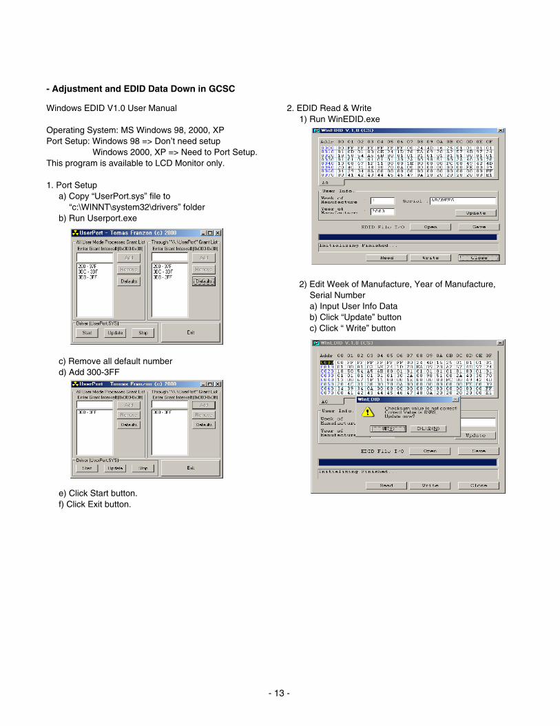
Windows EDID V1.0 User Manual
Operating System: MS Windows 98, 2000, XPPort Setup: Windows 98 => Don’t need setup
Windows 2000, XP => Need to Port Setup.This program is available to LCD Monitor only.
1. Port Setupa) Copy “UserPort.sys” file to
“c:\WINNT\system32\drivers” folderb) Run Userport.exe
c) Remove all default numberd) Add 300-3FF
e) Click Start button.f) Click Exit button.
2. EDID Read & Write1) Run WinEDID.exe
2) Edit Week of Manufacture, Year of Manufacture, Serial Numbera) Input User Info Datab) Click “Update” buttonc) Click “ Write” button
- Adjustment and EDID Data Down in GCSC

I
me P


47

6

1 2
Waveforms
Q901, Drain IC901, #6

,1,23,24

CHECKSCREEN CONTROL
KNOB OF FBT
CHECKVOLTAGE AT
D924 CATHODE (80V)
IC902 (12V)D921 CATHODE
(6.3V)?
CHECKIC401 (MICOM) PIN 16
5V (HIGH)
CHECKPOWER INDICATORGREEN or AMBER ?
- 21 -
3. NO RASTER
AMBER
NO
NO
NO
TROUBLE INIC401 (MICOM),
TROUBLE IN P302 SIGNAL CABLE
ROTATE SCREEN CONTROLKNOB TO CLOCKWISE or COUNTER CLOCKWIES
TROUBLE IN PRIMARY CIRCUIT OF T901
TROUBLE INPRIMARY CIRCUIT OF T901
GREEN
YES
YES
YES
NO VIDEO(POWER INDICATOR GREEN or AMBER)

CHECKIC601 PIN 7 (40V)?
CHECKIC601 PIN 1,2
(SAWTOOTH WAVE)?
CHECKIC601 Pin 3 (15V) ?
- 22 -
4. NO VERTICAL DEFLECTION
NO V-DEFLECTION(ONE HORIZONTAL LINE)
NO
NO
NO
TROUBLE INIC601, V-CIRCUIT
TROUBLE IN T901 15V Line
Waveforms
TROUBLE INT701 40V line
TROUBLE INIC401 OR R444,R445
YES
YES
YES
IC601, #1 IC601, #2
98
8 9

3
CHECKIC401 PIN 45,46 WAVEFORM?
CHECKIC401 PIN 25,26(0V)?
CHECK B+ LINE(50V, 15V,6.3V ,-12V 80V) ?
CHECKIC401 (MICOM)
PIN 52,53 (H/V INPUT) SIGNAL?
- 23 -
5. TROUBLE IN DPM
Stand-by/SUSPEND/DPMS OFF MODE FAILURE
INPUT H/V SYNC SIGNAL
NO
NO
NO
TROUBLE IN T901 or PC
CHECK PC,(PC IS NOT GOING INTO DPMMODE)
TROUBLE INX401
TROUBLE INIC401
TROUBLE INIC401
NO TROUBLE INQ912, Q914
NO H/V SYNC SIGNAL
YES
YES
YES
YES
DPMS TABLE
NORMAR ON/ON NORMAL GREEN
STAND-BY OFF/ON OFF(0V) AMBER
SUSPEND ON/OFF OFF(0V) AMBER
OFF OFF/OFF OFF(0V) AMBER
H/V SYNC VIDEO LEDMODE
ITEM
IC401, #45,46
CHECKIC401 PIN 16 (5V, HIGH)?
3
Waveforms

CHECKQ953 COLLECTOR VOLTAGE (0.5V)?
CHECKP902?
CHECKRL901?
CHECKIC401 PIN 4 (5V)?
6. NO DEGAUSSING
NO DEGAUSSING
NO
NO
NO
NO
TROUBLE IN TH901,
DEGAUSSING COIL
TROUBLE IN IC401 (MICOM)
TROUBLE IND952
TROUBLE INP902
TROUBLE INRL901
YES
YES
YES
YES
- 24 -

3


variable
R727 or C719
703

3

5


Proper Video levels areon P301 Pin 1, 3 and 5.
IC401 Pins 27 and 28inputs are right at
each function?
18. User Control Failure
Check connector Ass’y.
NO
Done.
Check and replace IC401.
Check and replace function key.
YES
19. Missing Color
NO
Done.
Change the CRT.
Check signal generator andsignal cable.
NORefer to 2 No Charcter.
NO Check and replace IC303and IC304
NO Check C341, C347 and G2 wire.Check around FBT circuits also.
YES
YES
YES
YES
- 32 -
Proper AC voltage areon all cathodes?
Proper DC voltage areon all cathodes?
G2 voltage is right?

Blank pedestal is on Pin 19, 20 and 21 of IC302
Is V_FLB and DC_bias onG1 Pin at CRT socket?
G2 voltage is right?
20. Visible Retrace
Check white balance adjustment.
NO
NO
NO
Done.
Check G2 control volume and FBT.
Check IC302and related components.
Check P302 Assy,
YES
YES
YES
21. Unsynchronized Image
Compare input sync. of IC401Pin52 and 53 with output sync.
of IC401 49 and 50.
NO
NO
NO
Done.
Check and replace IC401.
Check and replace IC401.
Check and replace IC401.
YES
YES
YES
- 33 -
Are they all right?
Are H_Out and V_Out of IC401 Pin 20,18
Are H_FLYBACK of IC401Pin 21 right?

2
5
3


2 M41QEU423X01NDDH LG-PHILIPS 95KHZ 29.1MM FLATRON


- 39 -
REPLACEMENT PARTS LIST
CAUTION: BEFORE REPLACING ANY OF THESE COMPONENTS, READ CAREFULLY THE SAFETY PRECAUTIONS IN THIS MANUAL.
* NOTE : S SAFETY MarkAL ALTERNATIVE PARTS
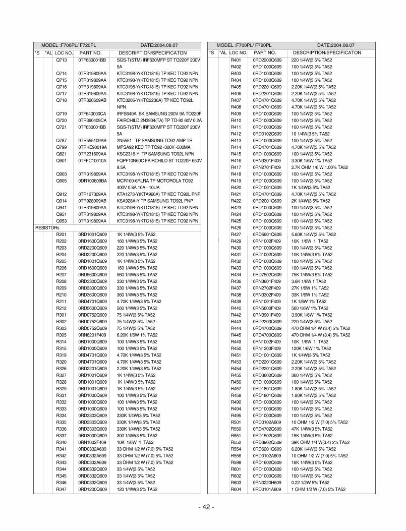
*S *AL LOC NO. PART NO. DESCRIPTION/SPECIFICATON
CAPACITORsC202 0CN1040K949 0.1M 50V Z F TA52C301 0CK1020K515 1000PF 50V K B TRC303 0CK1020K515 1000PF 50V K B TR
C304 181-288B MKT 100V 104JTR PHS26104C305 0CC2200W415 22PF 500V J NP0 TRC306 181-288N MKT 100V 103JTR PHS86103C308 0CE476CF638 “47UF SHL,SD 16V M FM5 TP 5”C309 0CK1040K945 0.1UF 50V Z F TRC310 181-288B MKT 100V 104JTR PHS26104C314 0CC4700W405 47PF 500V J SL TPC315 0CE227EF638 “220UF KMG,RD 16V 20% TP 5 FM5”C316 0CK1040K945 0.1UF 50V Z F TRC317 0CK1040K945 0.1UF 50V Z F TRC318 0CN1040K949 0.1M 50V Z F TA52C319 0CK1040K945 0.1UF 50V Z F TRC321 0CE225BK638 2.2U KME 50V M FM5 TP5C323 0CE476EF638 47UF KMG 16V M FM5 TP 5C324 0CN1040K949 0.1M 50V Z F TA52C325 181-288B MKT 100V 104JTR PHS26104C326 0CC1800K415 18P 50V J NPO TPC327 0CC1800K415 18P 50V J NPO TPC328 0CE476CN618 47UF SHL 100V M FL TP5C329 0CC1800K415 18P 50V J NPO TPC330 181-288B MKT 100V 104JTR PHS26104C331 181-288G MKT 100V 334JTR PHS26334C332 181-288G MKT 100V 334JTR PHS26334C333 181-288G MKT 100V 334JTR PHS26334C334 181-288B MKT 100V 104JTR PHS26104C335 181-288B MKT 100V 104JTR PHS26104C339 0CK4710W515 470P 500V K B TSC340 181-288B MKT 100V 104JTR PHS26104C341 0CK10301945 10000PF D 1KV Z F(Y5V) TRC344 181-288C MKT 100V 224JTR PHS 26224C345 0CZZTFT001R ECQB1H223JM3 223J 50V TP5.0
MATSUSHITAC346 0CK10301945 10000PF D 1KV Z F(Y5V) TRC347 0CK10301945 10000PF D 1KV Z F(Y5V) TRC350 0CK10301945 10000PF D 1KV Z F(Y5V) TRC355 0CE476CF638 “47UF SHL,SD 16V M FM5 TP 5”C358 0CN1040K949 0.1M 50V Z F TA52C359 0CN1040K949 0.1M 50V Z F TA52C360 0CN1040K949 0.1M 50V Z F TA52C372 0CK1040K945 0.1UF 50V Z F TRC401 0CK1040K945 0.1UF 50V Z F TRC403 0CK1040K945 0.1UF 50V Z F TRC404 0CK1040K945 0.1UF 50V Z F TRC405 0CE107CF638 “100UF SHL,SD 16V M FM5 TP 5”C406 0CK10102515 100PF D 2KV 10% B(Y5P) TRC407 0CQ4721N419 0.0047U 100V J POLY NI TP5C408 0CK1040K945 0.1UF 50V Z F TRC409 0CE106CK638 “10UF SHL,SD 50V M FM5 TP 5”C410 0CK1010K515 100PF 50V K B TRC411 0CK1010K515 100PF 50V K B TRC412 0CK1020K515 1000PF 50V K B TRC413 0CK1010K515 100PF 50V K B TRC414 0CE106CF638 “10UF SHL,SD 16V M FM5 TP 5”C415 0CQ4721N419 0.0047U 100V J POLY NI TP5C417 181-288B MKT 100V 104JTR PHS26104
C418 0CQ1031N419 0.01U 100V J POLY NI TPC419 181-476R 2200 D 100V H PP NI TP5C420 0CQ6831N509 0.068U 100V K POLY TPC421 0CQ1021N419 1000P 100V J POLY NI TPC422 0CK2220K515 2200P 50V K B TSC423 0CK2220K515 2200P 50V K B TSC424 0CE4756F618 4.7U SMS 16V M FL TP(5)C425 0CK2210K515 220P 50V K B TSC426 0CK1030K945 0.01UF 50V Z F TRC428 0CK1030K515 0.01UF D 50V 10% B(Y5P) TRC429 0CE3376F618 330M SMS 16V M FM5 TP5C501 0CE106CF638 “10UF SHL,SD 16V M FM5 TP 5”C502 0CK1040K945 0.1UF 50V Z F TRC601 0CE227EH638 “220UF KMG,RD 25V 20% FM5 TP 5”C602 181-288Q MKT 100V 154JTR PHS26154C603 0CE337CK618 330UF SHL 50V M FL TP5C604 0CQ6821N419 6800PF 100V J PE NI TPC605 0CK1020W515 1000P 500V K B TSC701 0CK1020K515 1000PF 50V K B TRC703 0CE108CF630 1000UF SHL 16V M FM5 BULKC705 181-477X 563J 19.5*15.5*9.0*7.5 250V J PU TP7.5C712 0CE106CK638 “10UF SHL,SD 50V M FM5 TP 5”C713 0CE1076F618 100UF SMS 16V M TP(5)C715 0CQ2221N419 2200PF 100V J PE NI TPC719 0CZZTAB001F SHL-BP SYE / SWE 50V 3.3UF 20% BULK
EB770HC722 181-477X 563J 19.5*15.5*9.0*7.5 250V J PU TP7.5C723 181-305B 124J 19.0*13.5*7.5*10.0 250V J MPP FM10C724 0CK1040K945 0.1UF 50V Z F TRC725 0CK6810W515 680P 500V K B TSC726 181-482J 394J 18.0*19.0*12.0*7.5 250V J MPP TP7.5C727 0CK1040K945 0.1UF 50V Z F TRC729 181-305L 684J 26.0*19.0*12.5*15.0 250V J MPP FM15C730 0CK1040K945 0.1UF 50V Z F TRC731 181-309F 222J 23.0*15.5*9.5*15.0 1.6KV J BUP FM15C733 0CBZTBU003G 332J 20.0*11.5*7.0*10.0 800V J BUP FM10C736 181-309F 222J 23.0*15.5*9.5*15.0 1.6KV J BUP FM15C737 181-477Y 683JF 20.0*16.5*9.5*7.5 250V J PU TP7.5C738 181-477Y 683JF 20.0*16.5*9.5*7.5 250V J PU TP7.5C739 0CE106EK638 10UF KMG 50V M FM5 TP 5C740 0CE337EL630 330UF KMG 63V 20% BULK FM5C741 0CZZTFT001Z ECQB1H104JM3 104J 50V TP5.0
MATSUSHITAC744 181-305Z “0.75UF D 250V 5%,-5% M/PP BULK”C745 0CK5610W515 560P 500V K B TSC746 0CK1510W515 150PF 500V K B TRC748 0CK1510W515 150PF 500V K B TRC749 0CE106CQ618 10UF SHL 200V M FL TP5C750 0CK1040K945 0.1UF 50V Z F TRC758 181-306M 822J 20.0*18.0*11.0*10.0 800V J PU FM10C767 0CK10301945 10000PF D 1KV Z F(Y5V) TRC771 0CK10301945 10000PF D 1KV Z F(Y5V) TRC775 0CK1040K945 0.1UF 50V Z F TRC801 0CE1074F638 “100UF SRA,SS 16V M FM5 TP 5”C803 181-288B MKT 100V 104JTR PHS26104C803 0CE1074F638 “100UF SRA,SS 16V M FM5 TP 5”C805 0CH6330K416 33PF 50V J NP0 2012 R/TPC806 0CE1074F638 “100UF SRA,SS 16V M FM5 TP 5”
*S *AL LOC NO. PART NO. DESCRIPTION/SPECIFICATON
MODEL :F700PL/ F720PL DATE:2004.08.07 MODEL :F700PL/ F720PL DATE:2004.08.07

MODEL :F700PL/ F720PL DATE:2004.08.07 MODEL :F700PL/ F720PL DATE:2004.08.07
C807 181-288B MKT 100V 104JTR PHS26104C807 0CE1054K638 “1 UF SRA,SS 50V M FM5 TP 5”C808 0DZ510009EE UDZ S 5.1B TP ROHM-K SOD323 200MW
5.1V 5MA .PFC809 0CH6330K416 33PF 50V J NP0 2012 R/TPC810 0CE1054K638 “1 UF SRA,SS 50V M FM5 TP 5”C812 0CH3103K516 10000PF 50V 10% B(Y5P) 2012 R/TPC813 0CK1030K945 0.01UF 50V Z F TRC820 0CH6470K416 47PF 50V 5% NP0 2012 R/TPC821 0CH6470K416 47PF 50V 5% NP0 2012 R/TPC822 0CK1040K945 0.1UF 50V Z F TRC822 0CH6470K416 47PF 50V 5% NP0 2012 R/TPC823 0CH6470K416 47PF 50V 5% NP0 2012 R/TPC830 0CK10102515 100PF D 2KV 10% B(Y5P) TRC831 0CH6470K416 47PF 50V 5% NP0 2012 R/TPC832 0CH6470K416 47PF 50V 5% NP0 2012 R/TPC850 0CH3104K946 100000PF 50V Z F 2012 R/TPC851 0CH3104K946 100000PF 50V Z F 2012 R/TPC901 0CZZTCB003C BULK 7.5 CS E 472M 14.5 250V TDKC902 0CZZTCB003C BULK 7.5 CS E 472M 14.5 250V TDKC903 0CK22101515 220P 1KV K B TP5C904 181-304V 393J 19.5*15.5*9.5*10.0 400V J PU FM10C905 181-124R 220UF SMG(25.4*40) 400V M VNSN BULKC906 0CE475CN638 “4.7UF SHL,SD 100V M FM5 TP 5”C907 0CE476CH638 “47UF SHL,SD 25V M FM5 TP 5”C908 0CK1040K945 0.1UF 50V Z F TRC909 0CK6810W515 680P 500V K B TSC910 0CZZTFT001N ECQB1H123JM3 123J 50V TP5.0
MATSUSHITAC911 0CE2266F618 22M SMS 16V M FM5 TP(5)C912 0CE225CK638 “2.2UF SHL,SD 50V M FM5 TP 5”C915 0CE476CH638 “47UF SHL,SD 25V M FM5 TP 5”C916 0CK2220K515 2200P 50V K B TSC918 0CZZTCB003C BULK 7.5 CS E 472M 14.5 250V TDKC919 0CZZTCB003C BULK 7.5 CS E 472M 14.5 250V TDKC920 0CE107CF638 “100UF SHL,SD 16V M FM5 TP 5”C921 0CE476CN618 47UF SHL 100V M FL TP5C922 0CE337EL630 330UF KMG 63V 20% BULK FM5C925 0CE228CH618 2200U SHL 25V M FL TP5C926 0CE108EF618 1000UF KMG 16V M FL TP 5C928 0CE108EF618 1000UF KMG 16V M FL TP 5C929 0CZZTFT001D ECQB1H222JM3 222J 50V TP5.0
MATSUSHITAC930 0CQ2721N419 2700PF 100V J PE NI TPC931 0CK56101515 560P 1KV K B TSC932 0CE227CF638 “220UF SHL,SD 16V M FM5 TP 5”C952 0CE477CH618 470UF SHL 25V M FL TP5
DIODEsZD401 0DZ560009AG GDZJ5.6B TP GRANDE DO-34 500MW 5.6V
5MAZD402 0DZ560009AG GDZJ5.6B TP GRANDE DO-34 500MW 5.6V
5MAZD403 0DZ560009AG GDZJ5.6B TP GRANDE DO-34 500MW 5.6V
5MAZD404 0DZ560009AG GDZJ5.6B TP GRANDE DO-34 500MW 5.6V
5MAZD405 0DZ560009AG GDZJ5.6B TP GRANDE DO-34 500MW 5.6V
5MAZD406 0DZ560009AG GDZJ5.6B TP GRANDE DO-34 500MW 5.6V
5MAZD408 0DZ560009AG GDZJ5.6B TP GRANDE DO-34 500MW 5.6V
5MAZD409 0DZ560009AG GDZJ5.6B TP GRANDE DO-34 500MW 5.6V
5MAZD702 0DZ510009BE GDZ5.1B TP GRANDE DO34 500MW 5.1V
20MA .PFZD801 0DZ510009EE UDZ S 5.1B TP ROHM-K SOD323 200MW
5.1V 5MA .PFZD802 0DZ510009EE UDZ S 5.1B TP ROHM-K SOD323 200MW
5.1V 5MA .PFZD803 0DZ510009EE UDZ S 5.1B TP ROHM-K SOD323 200MW
5.1V 5MA .PFZD804 0DZ510009EE UDZ S 5.1B TP ROHM-K SOD323 200MW
5.1V 5MA .PFZD805 0DZ510009EE UDZ S 5.1B TP ROHM-K SOD323 200MW
5.1V 5MA .PFZD806 0DZ510009EE UDZ S 5.1B TP ROHM-K SOD323 200MW
5.1V 5MA .PFZD811 0DZ560009DA UDZ S 5.6B TP ROHM-K SOD323 200MW
5.6V 5MA .PFZD812 0DZ560009DA UDZ S 5.6B TP ROHM-K SOD323 200MW
5.6V 5MA .PFD316 0DR140059DA “1N4005TB52 TP LITEON DO41 600V 1A
40A ,SEC 5UA”D403 0DS141489AB 1N4148 TP GRANDE DO-34 500MW 1
25NA(20V)D406 0DS124409AA 1SS244 TP ROHM KOREAD407 0DS141489AB 1N4148 TP GRANDE DO-34 500MW 1
25NA(20V)D553 0DS141489AB 1N4148 TP GRANDE DO-34 500MW 1
25NA(20V)D704 0DRSG00061A DMV1500HF5 SGS-THOMSON ST
TO220AB 600V/1500V 3A/6A 35A/80A 110NS/625NSSEC 20UA/100UA
D705 0DRGF00069A SB140 GULF TP DO41 40V 1A 40A .SEC 1MA
D706 0DRFC00020A FFPF10F150S FAIR CHILD BK TO220F 1500V 10A 100A 170NSSEC 10UA
D708 0DR140059DA “1N4005TB52 TP LITEON DO41 600V 1A 40A ,SEC 5UA”
D709 0DRGF00069A SB140 GULF TP DO41 40V 1A 40A .SEC 1MA
D710 0DR400409AC UF4004 GULF TP DO41 400V 1A 30A 50NSEC 10UA
D712 0DR100009CA RGP10G TP GULF SEMICONDUCTOR LTD. DO41 400V 1A 30A - 100UA
D714 0DS141489AB 1N4148 TP GRANDE DO-34 500MW 1 25NA(20V)
D715 0DS141489AB 1N4148 TP GRANDE DO-34 500MW 1 25NA(20V)
D716 0DR140059DA “1N4005TB52 TP LITEON DO41 600V 1A 40A ,SEC 5UA”
D717 0DR140059DA “1N4005TB52 TP LITEON DO41 600V 1A 40A ,SEC 5UA”
D718 0DR140059DA “1N4005TB52 TP LITEON DO41 600V 1A 40A ,SEC 5UA”
D719 0DR100009DA RGP10J TP GULF SEMICONDUCTOR LTD. DO41 600V 1A 30A - 100UA
D720 0DR140059DA “1N4005TB52 TP LITEON DO41 600V 1A 40A ,SEC 5UA”
D721 0DS141489AB 1N4148 TP GRANDE DO-34 500MW 1 25NA(20V)
D723 0DS141489AB 1N4148 TP GRANDE DO-34 500MW 1 25NA(20V)
D724 0DR100009DA RGP10J TP GULF SEMICONDUCTOR LTD. DO41 600V 1A 30A - 100UA
D730 0DS141489AB 1N4148 TP GRANDE DO-34 500MW 1 25NA(20V)
D768 0DR100009DA RGP10J TP GULF SEMICONDUCTOR LTD. DO41 600V 1A 30A - 100UA
- 40-
*S *AL LOC NO. PART NO. DESCRIPTION/SPECIFICATON*S *AL LOC NO. PART NO. DESCRIPTION/SPECIFICATON

MODEL :F700PL/ F720PL DATE:2004.08.07MODEL :F700PL/ F720PL DATE:2004.08.07
D801 0DS141489AB 1N4148 TP GRANDE DO-34 500MW 1 25NA(20V)
D802 0DS141489AB 1N4148 TP GRANDE DO-34 500MW 1 25NA(20V)
D821 0DS141489AB 1N4148 TP GRANDE DO-34 500MW 1 25NA(20V)
D835 0DRGF00069A SB140 GULF TP DO41 40V 1A 40A .SEC 1MA
D836 0DRGF00069A SB140 GULF TP DO41 40V 1A 40A .SEC 1MA
D901 0DRGF00090A GBL06 GULF BK GBL 600V 4A 120A .SEC 10UA
D902 0DRGF00109A GUF10M GULF TP DO41 1000V 1A 30A 75NSEC 10UA
D903 0DR100009CA RGP10G TP GULF SEMICONDUCTOR LTD.DO41 400V 1A 30A - 100UA
D904 0DR100009DA RGP10J TP GULF SEMICONDUCTOR LTD. DO41 600V 1A 30A - 100UA
D905 0DS141489AB 1N4148 TP GRANDE DO-34 500MW 1 25NA(20V)
D906 0DS141489AB 1N4148 TP GRANDE DO-34 500MW 1 25NA(20V)
D907 0DS141489AB 1N4148 TP GRANDE DO-34 500MW 1 25NA(20V)
D908 0DS141489AB 1N4148 TP GRANDE DO-34 500MW 1 25NA(20V)
D909 0DS141489AB 1N4148 TP GRANDE DO-34 500MW 1 25NA(20V)
D910 0DRGF00139A GPP20J GULF TP DO15 600V 2.0A 70A 2.0USSEC 5.0UA
D911 0DS141489AB 1N4148 TP GRANDE DO-34 500MW 1 25NA(20V)
D912 0DS141489AB 1N4148 TP GRANDE DO-34 500MW 1 25NA(20V)
D913 0DS141489AB 1N4148 TP GRANDE DO-34 500MW 1 25NA(20V)
D914 0DS141489AB 1N4148 TP GRANDE DO-34 500MW 1 25NA(20V)
D920 0DRSD00079A D2L20U SHINDENGEN TP DO-204AC 200V 1.5A 40A 35NSEC 10UA
D921 0DRSD00079A D2L20U SHINDENGEN TP DO-204AC 200V 1.5A 40A 35NSEC 10UA
D922 0DRGF00150A UF5404 GULF BK DO201AD 400V 3.0A 150A 50NSSEC 10.0UA
D923 0DRVH00091A GURF5H60 VISHAY ST ITO220 600V 5A 90A 30NSSEC 20UA
D924 0DR100009DA RGP10J TP GULF SEMICONDUCTOR LTD. DO41 600V 1A 30A - 100UA
D927 0DS141489AB 1N4148 TP GRANDE DO-34 500MW 1 25NA(20V)
D952 0DS141489AB 1N4148 TP GRANDE DO-34 500MW 1 25NA(20V)
CoilsL311 0LA0220K119 0.22UH K 2.3*3.4 TPL312 0LA0220K119 0.22UH K 2.3*3.4 TPL313 0LA0220K119 0.22UH K 2.3*3.4 TPL702 6140TBZ025A DR14*20 120UH 0.12*25MM 47.5T FB775BL703 6140TYZ011J 14*9T 3.4UH+/-20%H USTC0.12X30MM
19.5TL705 6140TBZ026F DR15*18-C9.8 55UH 0.10*45MM 33.5T D/D
CHOKEL706 150-985P DR12*15 6MH 0.25MM 365.5T H-
CENTERINGL801 6210TCE003P BRS2550B BO SUNG 2550MM RADIALL802 6210TCE003H BAS3510T BO SUNG 3510MM AXIAL52MM
L804 6210TCE001H HB-1T2012-301JT CERATEC 2012MM R/TPL805 6210TCE001H HB-1T2012-301JT CERATEC 2012MM R/TPL807 6210TCE001H HB-1T2012-301JT CERATEC 2012MM R/TPL808 6210TCE001H HB-1T2012-301JT CERATEC 2012MM R/TPL809 6210TCE001H HB-1T2012-301JT CERATEC 2012MM R/TPL810 6210TCE001H HB-1T2012-301JT CERATEC 2012MM R/TPL812 6210TCE003D BAS3514T BO SUNG 3514MM AXIAL52MML901 6140TBZ031B EE36SI PFC 49MH 0.5MM 228 +/- 10T .FB315 6210TCE003A BRD3510B BO SUNG 3510MM RADIALFB317 6210TCE003A BRD3510B BO SUNG 3510MM RADIALFB504 6210TCE003A BRD3510B BO SUNG 3510MM RADIALFB505 6210TCE003A BRD3510B BO SUNG 3510MM RADIALFB506 6210TCE003B BRS3580B BO SUNG 3580MM RADIALFB507 6210TCE003B BRS3580B BO SUNG 3580MM RADIALFB701 6210TCE003L BAS3580T BO SUNG 3580MM AXIAL52MMFB702 6210TCE003H BAS3510T BO SUNG 3510MM AXIAL52MMFB901 6210TCE003A BRD3510B BO SUNG 3510MM RADIALFB904 6210TCE003K BAS3550T BO SUNG 3550MM AXIAL52MMFB905 6210TCE003C BRD3514B BO SUNG 3514MM RADIALFB906 6210TCE003H BAS3510T BO SUNG 3510MM AXIAL52MMFB907 6210TCE003H BAS3510T BO SUNG 3510MM AXIAL52MMFB909 6210TCE003B BRS3580B BO SUNG 3580MM RADIALJ13 6210TCE003K BAS3550T BO SUNG 3550MM AXIAL52MMJ18 6210TCE003K BAS3550T BO SUNG 3550MM AXIAL52MM
ICsIC302 0IPRPNS025C “LM1246DDC/NA NATIONAL
SEMICONDUCTOR 24,DIP ST ONE CHIP (VIDEO+OSD)”
IC303 0IPRPNS014A “LM2465TA NATIONAL SEMICONDUCTOR 9P,TO220 ST MONOLITHIC TRIPLE 5.5NS CRT DRIVER”
IC304 0IPRPNS005A “LM2480NA NATIONAL SEMICONDUCTOR 8P,DIP ST 80V TRIPLE BIAS CLAMP”
IC401 0IMCRPH033A SAA4849(OTP) PHILIPS 56PIN SDIP - DEFLECTION AND MICOM
IC402 0IMMRSG044A M24C08-WBN6 STM 8PIN PDIP ST SERIAL IIC EEPROM
IC601 0IPRPPH018A “TDA4867J PHILIPS 9PIN,ST DIP VERTICALOUTPUT IC”
IC801 0IPH112200C “ISP1122ABD 32P,LQFP R/TP USB HUB IC”IC802 0ITI204200B TPS2042ADR TEXAS INSTRUMENT 8SOP
R/TP D/POWER DISTRIBUTION SWITCHIC901 0ISS384300A KA3843B 8P SDIP BK PWM CONTROLLERIC902 0IPMGFA069A “KA78R12C FAIRCHILD 4P,TO-220F-4L BK
1A LOW DROP REGULATOR”IC903 0ISS780500F KA7805
TRANSISTORsQ201 0TR319809AA KTC3198-Y(KTC1815) TP KEC TO92 NPNQ459 0TR319809AA KTC3198-Y(KTC1815) TP KEC TO92 NPNQ501 0TR320209AA KTC3202-Y(KTC1959) TP KEC TO92 NPNQ502 0TR127009AA KTA1270-Y(KTA562TM) TP KEC TO92 PNPQ551 0TR319809AA KTC3198-Y(KTC1815) TP KEC TO92 NPNQ552 0TR127009AA KTA1270-Y(KTA562TM) TP KEC TO92 PNPQ553 0TR320209AA KTC3202-Y(KTC1959) TP KEC TO92 NPNQ703 0TF630000CA IRFS630A BK SAMSUNG 200V 6.5A
TO220FQ704 0TR390409CA FAIRCHILD 2N3904(TA) TP TO-92 60V 0.2AQ705 0TFFC90002A IRFNL210B FAIRCHILD TP TO-92L 200V 1AQ706 0TRFC10012B FJAF6820L FAIRCHILD ST TO3PF 1550V
20A/30AQ710 0TRKE90020A MPSA44 KEC TP TO92 500V 300MAQ711 0TF630001BB SGS-T(STM) IRF630MFP ST TO220F 200V
5AQ712 0TF630001BB SGS-T(STM) IRF630MFP ST TO220F 200V
5A
*S *AL LOC NO. PART NO. DESCRIPTION/SPECIFICATON
- 41 -
*S *AL LOC NO. PART NO. DESCRIPTION/SPECIFICATON
MODEL :F700PL/ F720PL DATE:2004.08.07MODEL :F700PL/ F720PL DATE:2004.08.07
Q713 0TF630001BB SGS-T(STM) IRF630MFP ST TO220F 200V 5A
Q714 0TR319809AA KTC3198-Y(KTC1815) TP KEC TO92 NPNQ715 0TR319809AA KTC3198-Y(KTC1815) TP KEC TO92 NPNQ716 0TR319809AA KTC3198-Y(KTC1815) TP KEC TO92 NPNQ717 0TR319809AA KTC3198-Y(KTC1815) TP KEC TO92 NPNQ718 0TR320509AB KTC3205-Y(KTC2236A) TP KEC TO92L
NPNQ719 0TF640000CA IRFS640A BK SAMSUNG 200V 9A TO220FQ720 0TR390409CA FAIRCHILD 2N3904(TA) TP TO-92 60V 0.2AQ721 0TF630001BB SGS-T(STM) IRF630MFP ST TO220F 200V
5AQ787 0TR555109AB 2N5551 TP SAMSUNG TO92 AMP TRQ799 0TRKE90019A MPSA92 KEC TP TO92 -300V -500MAQ821 0TR231609AA KSC2316-Y TP SAMSUNG TO92L NPNQ901 0TFFC10010A FQPF10N60C FAIRCHILD ST TO220F 650V
9.5AQ903 0TR319809AA KTC3198-Y(KTC1815) TP KEC TO92 NPNQ905 0DR100609BA MCR100-6RLRA TP MOTOROLA TO92
400V 0.8A 10A - 10UAQ912 0TR127309AA KTA1273-Y(KTA966A) TP KEC TO92L PNPQ914 0TR928009AB KSA928A-Y TP SAMSUNG TO92L PNPQ941 0TR319809AA KTC3198-Y(KTC1815) TP KEC TO92 NPNQ951 0TR319809AA KTC3198-Y(KTC1815) TP KEC TO92 NPNQ953 0TR319809AA KTC3198-Y(KTC1815) TP KEC TO92 NPN
RESISTORsR201 0RD1001Q609 1K 1/4W(3 5% TA52R202 0RD1600Q609 160 1/4W(3 5% TA52R203 0RD2200Q609 220 1/4W(3 5% TA52R204 0RD2200Q609 220 1/4W(3 5% TA52R205 0RD1001Q609 1K 1/4W(3 5% TA52R206 0RD1600Q609 160 1/4W(3 5% TA52R207 0RD5600Q609 560 1/4W(3 5% TA52R208 0RD3300Q609 330 1/4W(3 5% TA52R209 0RD3300Q609 330 1/4W(3 5% TA52R210 0RD3600Q609 360 1/4W(3 5% TA52R211 0RD4701Q609 4.70K 1/4W(3 5% TA52R212 0RD5600Q609 560 1/4W(3 5% TA52R301 0RD0752Q609 75 1/4W(3 5% TA52R302 0RD0752Q609 75 1/4W(3 5% TA52R303 0RD0752Q609 75 1/4W(3 5% TA52R305 0RN6201F409 6.20K 1/6W 1% TA52R314 0RD1000Q609 100 1/4W(3 5% TA52R315 0RD1000Q609 100 1/4W(3 5% TA52R319 0RD4701Q609 4.70K 1/4W(3 5% TA52R320 0RD4701Q609 4.70K 1/4W(3 5% TA52R326 0RD2201Q609 2.20K 1/4W(3 5% TA52R327 0RD1001Q609 1K 1/4W(3 5% TA52R328 0RD1001Q609 1K 1/4W(3 5% TA52R329 0RD1001Q609 1K 1/4W(3 5% TA52R331 0RD1000Q609 100 1/4W(3 5% TA52R332 0RD1000Q609 100 1/4W(3 5% TA52R333 0RD1000Q609 100 1/4W(3 5% TA52R334 0RD3303Q609 330K 1/4W(3 5% TA52R335 0RD3303Q609 330K 1/4W(3 5% TA52R336 0RD3303Q609 330K 1/4W(3 5% TA52R337 0RD3000Q609 300 1/4W(3 5% TA52R340 0RN1002F409 10K 1/6W 1 TA52R341 0RD0332A609 33 OHM 1/2 W (7.0) 5% TA52R342 0RD0332A609 33 OHM 1/2 W (7.0) 5% TA52R343 0RD0332A609 33 OHM 1/2 W (7.0) 5% TA52R344 0RD0332Q609 33 1/4W(3 5% TA52R345 0RD0332Q609 33 1/4W(3 5% TA52R346 0RD0332Q609 33 1/4W(3 5% TA52R347 0RD1200Q609 120 1/4W(3 5% TA52
R401 0RD2200Q609 220 1/4W(3 5% TA52R402 0RD1000Q609 100 1/4W(3 5% TA52R403 0RD1000Q609 100 1/4W(3 5% TA52R404 0RD1000Q609 100 1/4W(3 5% TA52R405 0RD2201Q609 2.20K 1/4W(3 5% TA52R406 0RD2201Q609 2.20K 1/4W(3 5% TA52R407 0RD4701Q609 4.70K 1/4W(3 5% TA52R408 0RD4701Q609 4.70K 1/4W(3 5% TA52R409 0RD1000Q609 100 1/4W(3 5% TA52R410 0RD1000Q609 100 1/4W(3 5% TA52R411 0RD1000Q609 100 1/4W(3 5% TA52R412 0RD0102Q609 10 1/4W(3 5% TA52R413 0RD1000Q609 100 1/4W(3 5% TA52R414 0RD4701Q609 4.70K 1/4W(3 5% TA52R415 0RD1000Q609 100 1/4W(3 5% TA52R416 0RN3301F409 3.30K 1/6W 1% TA52R417 0RN2701F409 2.7K OHM 1/6 W 1.00% TA52R418 0RD1000Q609 100 1/4W(3 5% TA52R419 0RD1000Q609 100 1/4W(3 5% TA52R420 0RD1001Q609 1K 1/4W(3 5% TA52R421 0RD4701Q609 4.70K 1/4W(3 5% TA52R422 0RD2001Q609 2K 1/4W(3 5% TA52R423 0RD1000Q609 100 1/4W(3 5% TA52R424 0RD1000Q609 100 1/4W(3 5% TA52R425 0RD1000Q609 100 1/4W(3 5% TA52R426 0RD1000Q609 100 1/4W(3 5% TA52R427 0RD5601Q609 5.60K 1/4W(3 5% TA52R429 0RN1002F409 10K 1/6W 1 TA52R430 0RD1000Q609 100 1/4W(3 5% TA52R431 0RD1002Q609 10K 1/4W(3 5% TA52R432 0RD1000Q609 100 1/4W(3 5% TA52R433 0RD1000Q609 100 1/4W(3 5% TA52R434 0RD7502Q609 75K 1/4W(3 5% TA52R436 0RN3601F409 3.6K 1/6W 1 TA52R437 0RN2702F409 27K 1/6W 1% TA52R438 0RN3302F409 33K 1/6W 1% TA52R439 0RN1001F409 1K 1/6W 1% TA52R440 0RN5600F409 560 1/6W 1% TA52R442 0RN3901F409 3.90K 1/6W 1% TA52R443 0RD2200Q609 220 1/4W(3 5% TA52R444 0RD4700Q609 470 OHM 1/4 W (3.4) 5% TA52R445 0RD4700Q609 470 OHM 1/4 W (3.4) 5% TA52R449 0RN1002F409 10K 1/6W 1 TA52R450 0RN1203F409 120K 1/6W 1% TA52R451 0RD1001Q609 1K 1/4W(3 5% TA52R453 0RD2201Q609 2.20K 1/4W(3 5% TA52R454 0RD2201Q609 2.20K 1/4W(3 5% TA52R455 0RD3600Q609 360 1/4W(3 5% TA52R456 0RD1000Q609 100 1/4W(3 5% TA52R457 0RD1801Q609 1.80K 1/4W(3 5% TA52R458 0RD1801Q609 1.80K 1/4W(3 5% TA52R490 0RD1000Q609 100 1/4W(3 5% TA52R494 0RD1000Q609 100 1/4W(3 5% TA52R495 0RD1000Q609 100 1/4W(3 5% TA52R501 0RD0102A609 10 OHM 1/2 W (7.0) 5% TA52R550 0RD4702Q609 47K 1/4W(3 5% TA52R551 0RD1502Q609 15K 1/4W(3 5% TA52R552 0RD3902Q509 39K OHM 1/4 W(3.4) 2% TA52R554 0RD6201Q609 6.20K 1/4W(3 5% TA52R556 0RD0102A609 10 OHM 1/2 W (7.0) 5% TA52R598 0RD1602Q609 16K 1/4W(3 5% TA52R601 0RD1000Q609 100 1/4W(3 5% TA52R602 0RD1000Q609 100 1/4W(3 5% TA52R603 0RN0220H609 0.22 1/2W 5% TA52R604 0RD0101A609 1 OHM 1/2 W (7.0) 5% TA52
- 42 -
*S *AL LOC NO. PART NO. DESCRIPTION/SPECIFICATON*S *AL LOC NO. PART NO. DESCRIPTION/SPECIFICATON

MODEL :F700PL/ F720PL DATE:2004.08.07MODEL :F700PL/ F720PL DATE:2004.08.07
R605 0RD0331A609 3.3 OHM 1/2 W (7.0) 5% TA52R606 0RD1000A609 100 OHM 1/2 W (7.0) 5% TA52R607 0RN4701F409 4.70K 1/6W 1% TA52R608 0RD1600A609 160 OHM 1/2 W (7.0) 5% TA52R701 0RD6800Q609 680 1/4W(3 5% TA52R702 0RD6800Q609 680 1/4W(3 5% TA52R703 0RD5101A609 5.1K OHM 1/2 W (7.0) 5% TA52R704 0RD5101Q609 5.10K 1/4W(3 5% TA52R706 0RN0102G609 10 1/4W 5 TA52R707 0RD3302A609 33K OHM 1/2 W (7.0) 5% TA52R708 0RD5600A609 560 OHM 1/2 W (7.0) 5% TA52R711 0RD7502Q609 75K 1/4W(3 5% TA52R729 0RD3301Q609 3.30K 1/4W(3 5% TA52R730 0RMZTWD001N PRZC-1 UNI-OHM 1.1OHM 5 W 5% RWR
PD-TYPER731 0RD4702Q609 47K 1/4W(3 5% TA52R732 0RD1001Q609 1K 1/4W(3 5% TA52R734 0RN0390J607 0.39 1W 5% TA62R735 0RD1002Q609 10K 1/4W(3 5% TA52R736 0RX2201K665 2200 OHM 2 W 5% SFR739 0RD1001Q609 1K 1/4W(3 5% TA52R740 0RD0332A609 33 OHM 1/2 W (7.0) 5% TA52R743 0RD2000Q609 200 1/4W(3 5% TA52R744 0RX1100K607 110 OHM 2 W 5.00% TA62R745 0RD4702Q609 47K 1/4W(3 5% TA52R746 0RD2201Q609 2.20K 1/4W(3 5% TA52R747 0RD3001Q609 3K 1/4W(3 5% TA52R748 0RD4702Q609 47K 1/4W(3 5% TA52R749 0RD2201Q609 2.20K 1/4W(3 5% TA52R750 0RD3001Q609 3K 1/4W(3 5% TA52R751 0RD0222A609 22 OHM 1/2 W (7.0) 5% TA52R752 0RD2201Q609 2.20K 1/4W(3 5% TA52R753 0RD3001Q609 3K 1/4W(3 5% TA52R754 0RX6800K607 680 OHM 2 W 5% TA62R755 0RD3001Q609 3K 1/4W(3 5% TA52R756 0RD2202A609 22K OHM 1/2 W (7.0) 5% TA52R758 0RD2201Q609 2.20K 1/4W(3 5% TA52R761 0RD3001Q609 3K 1/4W(3 5% TA52R762 0RD3001Q609 3K 1/4W(3 5% TA52R763 0RD3001Q609 3K 1/4W(3 5% TA52R764 0RD3001Q609 3K 1/4W(3 5% TA52R765 0RD1000A609 100 OHM 1/2 W (7.0) 5% TA52R768 0RD4303A609 430K OHM 1/2 W (7.0) 5% TA52R771 0RD1101A609 1.1K OHM 1/2 W (7.0) 5% TA52R772 0RN3302F409 33K 1/6W 1% TA52R773 0RN1303H409 130K OHM 1/2 W 1% TA52R775 0RD4702Q609 47K 1/4W(3 5% TA52R780 0RD2202Q609 22K 1/4W(3 5% TA52R781 0RD2001Q609 2K 1/4W(3 5% TA52R782 0RD3301A609 3.3K OHM 1/2 W(7.0) 5.00% TA52R785 0RD0471A609 4.7 OHM 1/2 W (7.0) 5% TA52R788 0RD4702Q609 47K 1/4W(3 5% TA52R793 0RD4702Q609 47K 1/4W(3 5% TA52R799 0RD1502Q609 15K 1/4W(3 5% TA52R801 0RH1502D622 15K 1/10W 5 D.R/TPR802 0RH1502D622 15K 1/10W 5 D.R/TPR803 0RD2001Q609 2K 1/4W(3 5% TA52R803 0RH1502D622 15K 1/10W 5 D.R/TPR804 0RD0222Q609 22 1/4W(3 5% TA52R805 0RD0222Q609 22 1/4W(3 5% TA52R806 0RD0222Q609 22 1/4W(3 5% TA52R807 0RH1502D622 15K 1/10W 5 D.R/TPR808 0RH0222D622 22 OHM 1 / 10 W 2012 5.00% DR809 0RX0151L665 1.5 OHM 3 W 5% SFR809 0RH1004D622 1.0M 1/10W 5 D.R/TP
R810 0RH1004D622 1.0M 1/10W 5 D.R/TPR811 0RH1003D622 100K 1/10W 5 D.R/TPR812 0RH1003D622 100K 1/10W 5 D.R/TPR813 0RH1004D622 1.0M 1/10W 5 D.R/TPR814 0RH1004D622 1.0M 1/10W 5 D.R/TPR817 0RH0222D622 22 OHM 1 / 10 W 2012 5.00% DR818 0RN6202F409 62KOHM 1/6 W 1% TA52R821 0RH1501D622 1.5K OHM 1 / 10 W 2012 5.00% DR822 0RD0122A609 12 OHM 1/2 W (7.0) 5% TA52R823 0RX0432K665 43OHM 2 W 5% SFR828 0RH0222D622 22 OHM 1 / 10 W 2012 5.00% DR829 0RH1002D622 10K OHM 1 / 10 W 2012 5.00% DR830 0RH1002D622 10K OHM 1 / 10 W 2012 5.00% DR835 0RH1003D622 100K 1/10W 5 D.R/TPR836 0RH1004D622 1.0M 1/10W 5 D.R/TPR837 0RH3301D622 3.3K 1/10W 5 D.R/TPR841 0RH1502D622 15K 1/10W 5 D.R/TPR842 0RH1502D622 15K 1/10W 5 D.R/TPR850 0RH1502D622 15K 1/10W 5 D.R/TPR851 0RH1502D622 15K 1/10W 5 D.R/TPR869 0RX0332K665 33 OHM 2 W 5% SFR870 0RX0122K607 12 OHM 2 W 5% TA62R872 0RD2401Q609 2.40K 1/4W(3 5% TA52R902 0RD0102Q609 10 1/4W(3 5% TA52R903 0RD0512Q609 51 1/4W(3 5% TA52R905 0RX1003K607 100KOHM 2 W 5% TA62R906 0RX1003K607 100KOHM 2 W 5% TA62R907 0RN1800F409 180 OHM 1/6 W 1.00% TA52R908 0RN0220H609 0.22 1/2W 5% TA52R909 0RD1002Q609 10K 1/4W(3 5% TA52R910 0RN1602F409 16K 1/6W 1% TA52R911 0RN2001F409 2K OHM 1/6 W 1.00% TA52R912 0RD1001Q609 1K 1/4W(3 5% TA52R913 0RB0120K607 0.12 OHM 2 W 5% TA62R914 0RD6800Q609 680 1/4W(3 5% TA52R915 0RD3903A609 390K OHM 1/2 W (7.0) 5% TA52R916 0RD3603A609 360K OHM 1/2 W (7.0) 5% TA52R917 0RD0622Q609 62 OHM 1/4 W(3.4) 5.00% TA52R918 0RD1003Q609 100K 1/4W(3 5% TA52R920 0RD0392Q609 39 1/4W(3 5% TA52R921 0RD0332Q609 33 1/4W(3 5% TA52R922 0RD5601Q609 5.60K 1/4W(3 5% TA52R923 0RD1001Q609 1K 1/4W(3 5% TA52R924 0RD4703Q609 470K 1/4W(3 5% TA52R925 0RD1501Q609 1.50K 1/4W(3 5% TA52R926 0RD4701Q609 4.70K 1/4W(3 5% TA52R929 0RN0220H609 0.22 1/2W 5% TA52R930 0RN0220H609 0.22 1/2W 5% TA52R931 0RD1000Q609 100 1/4W(3 5% TA52R933 0RD0472Q609 47 1/4W(3 5% TA52R934 0RD3302Q609 33K 1/4W(3 5% TA52R935 0RD3301Q609 3.30K 1/4W(3 5% TA52R936 0RX3902K665 39K OHM 2 W 5% SFR941 0RD6802A609 68K OHM 1/2 W (7.0) 5% TA52R944 0RD4700A609 470 OHM 1/2 W (7.0) 5% TA52R945 0RD1000Q609 100 1/4W(3 5% TA52R949 0RN0220H609 0.22 1/2W 5% TA52R951 0RN0220H609 0.22 1/2W 5% TA52R953 0RD1101A609 1.1K OHM 1/2 W (7.0) 5% TA52R954 0RD4701Q609 4.70K 1/4W(3 5% TA52R955 0RD5101Q609 5.10K 1/4W(3 5% TA52R957 0RD0512Q609 51 1/4W(3 5% TA52R991 0RD5101Q609 5.10K 1/4W(3 5% TA52
OthersRL901 6920TBB007A JZC-42012-2HS HONGMEI 250VAC 5A 12V
- 43-
*S *AL LOC NO. PART NO. DESCRIPTION/SPECIFICATON*S *AL LOC NO. PART NO. DESCRIPTION/SPECIFICATON

MODEL :F700PL/ F720PL DATE:2004.08.07MODEL :F700PL/ F720PL DATE:2004.08.07
2A NO VENTINGSC301 6620TBD003A PCS701E PARK ELEC. 10PIN 14/360
STRAIGHTSC901 6200TJB001G 02MD3P DELTA BK CB777FSG301 6918TAT007A KSA-201-MA Y&Y UNICTRON AXIAL
TAPINGSG302 6918TAT007A KSA-201-MA Y&Y UNICTRON AXIAL
TAPINGSG303 6918TAT007A KSA-201-MA Y&Y UNICTRON AXIAL
TAPINGSG305 6918TRT004B SG5-152-CB Y&Y UNICTRON RADIAL
TAPINGSG701 6918TRT004B SG5-152-CB Y&Y UNICTRON RADIAL
TAPINGSW201 6600R00001A “JTP1280F6 JEIL 12V DC 1MA
VERTICAL,7MM”SW202 6600R00001A “JTP1280F6 JEIL 12V DC 1MA
VERTICAL,7MM”SW203 6600R00001A “JTP1280F6 JEIL 12V DC 1MA
VERTICAL,7MM”SW204 6600R00001A “JTP1280F6 JEIL 12V DC 1MA
VERTICAL,7MM”SW205 6600R00001A “JTP1280F6 JEIL 12V DC 1MA
VERTICAL,7MM”SW206 6600R00001A “JTP1280F6 JEIL 12V DC 1MA
VERTICAL,7MM”SW250 6600M000020 “2216F DAE JIN 30VDC 0.1A 250GF,BLUE
ANGEL”SW801 140-079D “JLS1301 JEIL 36V 200MA LEVER S/W,JEIL”T701 6174T11005G “CF2172LG3900, T910BL(98KHZ),13MM
LIEN CHANG 19”””T702 6170TCZ013B EI2218 26UH D/FOCUS F700PLT703 6170TCZ008A EE2218 1.3MH FB995CT901 6170TMZ155A EER4045 150UH V-18PIN F700PL
SI/TC/SC/NY 98KHZTH901 6322B00002D MZ72-4.5RN290V GAOLI 4.5OHM +30% -
20% 2PIN BOXVR901 180-035D “EVN-DJAA03B32 (MEC),300B”X401 6212AA2003E HC-49U SOUTH STAR 48MHZ +/- 20 PPM
22PF BULKX801 6202TTB002B ATS-49/U SUNNY RADIAL 6MHZ 30PPM
16PF BK
- 44 -
*S *AL LOC NO. PART NO. DESCRIPTION/SPECIFICATON*S *AL LOC NO. PART NO. DESCRIPTION/SPECIFICATON


Aug. 2004P/NO : 3828TSL105A Printed in China