Embed Size (px)
Citation preview
See discussions, stats, and author profiles for this publication at: https://www.researchgate.net/publication/2983446
60 GHz Single-Chip Front-End MMICs and Systems for Multi-Gb/s Wireless
Communication
Article in IEEE Journal of Solid-State Circuits · June 2007
DOI: 10.1109/JSSC.2007.894824 · Source: IEEE Xplore
CITATIONS
76READS
717
10 authors, including:
Some of the authors of this publication are also working on these related projects:
High-efficiency optical phase modulators View project
SOCRA project View project
Camilla Kärnfelt
Institut Mines-Télécom, IMT Atlantique Bretagne Pays de la Loire, Brest, France
84 PUBLICATIONS 677 CITATIONS
SEE PROFILE
Herbert Zirath
Chalmers University of Technology
492 PUBLICATIONS 9,818 CITATIONS
SEE PROFILE
Rumen Kozhuharov
Chalmers University of Technology
70 PUBLICATIONS 704 CITATIONS
SEE PROFILE
Dan Kuylenstierna
Chalmers University of Technology
87 PUBLICATIONS 1,252 CITATIONS
SEE PROFILE
All content following this page was uploaded by Camilla Kärnfelt on 13 December 2012.
The user has requested enhancement of the downloaded file.

Manuscript for JSSC
1
60 GHz Single-Chip Front-End MMICs and Systems
for Multi-Gbps Wireless Communication
AUTHORS
Sten E. Gunnarsson1, Student Member, IEEE Camilla Kärnfelt1, Member, IEEE Herbert Zirath1,2, Member, IEEE
Rumen Kozhuharov1 Dan Kuylenstierna1, Student Member, IEEE
Christian Fager1, Member, IEEE Mattias Ferndahl1
Bertil Hansson1
Arne Alping2, Member, IEEE Paul Hallbjörner2,3
Per Ligander2
AUTHOR AFFILIATIONS 1 Microwave Electronics Laboratory Dept. of Microtechnology and Nanoscience, MC2 Chalmers University of Technology SE-412 96 Göteborg Sweden 2 Microwave and High Speed Electronics Research Center (MHSERC) Ericsson AB SE -431 84 Mölndal Sweden 3 SP - Swedish National Testing and Research Institute Box 857 SE -501 15 Borås Sweden
CORRESPONDING AUTHOR CONTACT INFORMATION Sten E. Gunnarsson
Microwave Electronics Laboratory Dept. of Microtechnology and Nanoscience, MC2 Chalmers University of Technology SE -412 96 Göteborg SWEDEN
Phone: +46 (31) 772 18 94 Fax: +46 (31) 16 45 13 E-mail: [email protected]

Manuscript for JSSC
2
Abstract — Single-chip 60 GHz transmitter (TX) and receiver (RX) MMICs have been designed and characterized in a 0.15 µm (fT
~120 GHz / fMAX >200 GHz) GaAs mHEMT MMIC process. This paper describes the second generation of single-chip TX and RX
MMICs together with work on packaging (e.g. flip-chip), substrate integrated antennas and system measurements. Compared to the
first generation of the designs in a commercial pHEMT technology, the MMICs presented in this paper show the same high level of
integration but occupy smaller chip area and have higher gain and output power at only half the DC power consumption. The system
operates with an LO signal in the range of 7 – 8 GHz. This LO signal is multiplied in an integrated multiply-by-eight (X8) LO chain,
resulting in an IF center frequency of 2.5 GHz. Although not integrated in the presented TX and RX MMICs, an mHEMT based VCO
suitable for future integration is also presented.
Packaging and interconnects are discussed and a module where the TX and RX MMICs are wire bonded to an alumina substrate is
presented. As an alternative to wire bonding, flip-chip assembly tests are presented and discussed. Substrate integrated antennas for
small, compact, and cheap TX and RX modules are also shown.
Finally, system measurements are described where bit error rate (BER) and eye diagrams are measured when the presented TX and
RX MMICs transmits and receives a modulated signal. These tests indicate that the presented MMICs are especially well suited for
transmission and reception of wireless signals at data rates of several Gbps.
Index Terms—60 GHz, flip-chip, GaAs, highly integrated, image rejection, mHEMT, MMIC, multi-functional, packaging, receiver,
RX, single-chip, substrate integrated antennas, transmitter, TX, V-band.
I. INTRODUCTION
A1 key term for future communication networks is “quadruple play,” i.e., providing a simultaneous service for voice, video,
data, as well as mobility or nomadism, i.e. connected everywhere. This requires wireless access networks with very high capacity.
High data-rate wireless access requires broad frequency bands, and a sufficiently broadband spectrum can be obtained in the
millimeter-wave (mm-wave) bands. The mm-wave band has several advantages: large spectral capacity, small antennas, and
compact and light equipment. In the 60 GHz band, where the oxygen absorption has its maximum (10 – 15 dB/km), there is also the
additional benefit of reduced co-channel interference. Therefore, this mm-wave band enables dense (< 1 km) wireless
communication, due to shorter cell re-use distance, as well as access to worldwide allocated non-regulatory frequency bands [1-3].
Today, several companies provide 60 GHz data links for Gigabit Ethernet (1.25 Gbps) bridges between LAN networks. It is
expected that the use of 60 GHz technologies will extend to other areas, such as fixed wireless access networks [3]. Inter-vehicle
1 Manuscript received July 7 2006. This work was supported in part by the Swedish Foundation for Strategic Research (SSF) the Swedish Agency for Innovation
Systems (VINNOVA), Ericsson AB, and Chalmers Center for High Speed Technology (CHACH).
S. E. Gunnarsson, C. Kärnfelt, H. Zirath, R. Kozhuharov, D. Kuylenstierna, C. Fager, M. Ferndahl, and B. Hansson are with the Microwave Electronics Laboratory,
Dept. of Microtechnology and Nanoscience – MC2, Chalmers University of Technology, Göteborg, Sweden. (e-mail: [email protected]).
H. Zirath is also with Ericsson AB, MHSERC, Mölndal, Sweden together with A. Alping and P. Ligander.
P. Hallbjörner was at the time the work was performed with Ericsson AB, MHSERC, Mölndal, Sweden but is currently with SP - Swedish National Testing and
Research Institute, Borås, Sweden.
60 GHz Single-Chip Front-End MMICs and Systems for Multi-Gbps Wireless Communication
Sten E. Gunnarsson, Student Member, IEEE, Camilla Kärnfelt, Member, IEEE, Herbert Zirath, Member, IEEE,
Rumen Kozhuharov, Dan Kuylenstierna, Student Member, IEEE, Christian Fager, Member, IEEE, Mattias Ferndahl, Student Member, IEEE, Bertil Hansson, Arne Alping, Member, IEEE, Paul Hallbjörner, and Per Ligander.

Manuscript for JSSC
3
and roadside communications in Intelligent Transport System (ITS) applications, as well as the quasi-cellular Mobile Broadband
Systems (MBS) [4], are other areas where 60 GHz technologies will be implemented in the future.
The ultimate application area would certainly be for 60 GHz WLAN and WPAN, which would require mass production of
small, low-cost, and highly integrated transceiver products dedicated for scenarios including hot spots in vendor areas and
cyber-cafés, high-density residential dwellings and flats, and corporate environments [5]. In Japan, there has been an extensive
effort to implement 60 GHz technologies for the wireless home, e.g., the wireless video Home-Link systems [6], which includes
applications such as Wireless 1394 (FireWire).
During the last few years, a number of publications describing MMIC chip-sets suitable for broadband 60 GHz applications
have been published [6]–[13], but for all the applications mentioned above, it is important to reduce the number of interconnects
and the cost of the chip itself. A high integration level is therefore necessary and a single MMIC chip should contain as much as
possible of the mm-wave front-end. Most of the published results are based on GaAs technology, although SiGe [13] or even
CMOS has been considered [14]. Silicon-based technologies are potentially beneficial due to the possible integration with digital
electronics and from a cost perspective, but the latter is only valid for very large-scale production. High integration will also relax
the cost issue for compound semiconductor technologies.
Recently, our group at Chalmers University of Technology has presented highly integrated 60 GHz transmitter (TX) and
receiver (RX) chips using a commercial foundry process based on a 0.15 µm gate length GaAs pHEMT technology2 [15]. This
paper reports on the continuation of the work presented in [16] and reports on the development of the second generation of 60 GHz
TX and RX chips using a foundry process based on a 0.15 µm gate length GaAs mHEMT technology3 are presented. Together with
[13] and [15], these chips show the highest level of integration yet presented in the 60 GHz band.
Packaging and interconnects are also important issues when integrating the MMIC chips into a complete transceiver module.
This paper presents a module where the TX and RX MMICs are wire bonded to an alumina substrate. As an alternative to wire
bonding, flip-chip assembly tests have been evaluated and are also presented and discussed.
The small size (a few mm2) of an antenna at these frequencies opens up the possibility of incorporating the antennas into the
package. Using advanced multi-functional MCM structures, it is possible to integrate planar antennas with an MMIC chip-set
performing transmit and receive functions in a 60 GHz module, which is also discussed in this paper.
The paper is outlined as follows: section II presents the used MMIC technology. Section III shows an overview of the TX and
RX chips. Section IV – VI presents the design and measured results of the local signal generation chain and the VCO, up and down
converting mixers and the three-stage amplifier used as both post amplifier (PA) in the TX and low noise amplifier (LNA) in the
RX MMIC. Section VII and VIII presents the measured results of the TX and RX chips, respectively. Packaging and interconnect
issues including flip-chip assembly are presented and discussed in section IX and substrate integrated antennas are shown in
section X. Thereafter, system level measurements with the TX and RX chips interconnected are presented in section XI. A
discussion and summary is found in section XII and finally, section XIII concludes the presented material.
II. MMIC TECHNOLOGY
In this work, an mHEMT MMIC process from WIN Semiconductors in Taiwan was used3. The device structures are grown by
molecular beam epitaxy (MBE) on a semi-insulating GaAs substrate. For device fabrication, E-beam lithography is used to define
the 0.15 μm gate; Au/Ge/Ni/Au metals are evaporated and alloyed with a rapid thermal processing (RTP) system providing a low
2 WIN pp15-20 0.15μm pHEMT – www.winfoundry.com

Manuscript for JSSC
4
contact resistance around 0.15 Ω-mm. Concerning high frequency characteristics, the devices show a cut-off frequency (fT) of 120
GHz and a maximum oscillation frequency (fMAX) exceeding 200 GHz. Regarding passive components, TaN resistors with a sheet
resistance of 50±1 Ω/square was fabricated together with MIM capacitors with a capacitance of 400±40 pF/mm2. Measured
transconductance (gm) and drain current (ID) characteristics versus VGS are found in Fig. 1 for a 2×50 μm mHEMT device.
Maximum ID density was 730 mA/mm.
The first generation of 60 GHz single-chip TX and RX MMICs developed in our group at Chalmers University of Technology,
[15], used a 0.15 μm gate length pHEMT technology2 from the same foundry as provided the mHEMT technology. The passive
components in the pHEMT technology were identical to the ones used in the mHEMT counterpart. However, the pHEMT devices
showed a fT of 88±2.2 GHz and an fMAX of 183±11.2 GHz for volume production wafers. Concerning DC characteristics,
maximum gm and ID were measured to 490 mS/mm and 660 mA/mm, respectively. The pinch-off voltage was found to be -1.1 V
which is 400 mV lower, i.e. more negative, compared to its mHEMT counterpart.
In circuits like resistive mixers where the HEMT device operates as a gate-voltage controlled resistor with zero drain bias, rDS
versus VGS is an important parameter. For maximum conversion efficiency in such circuits, the HEMT would ideally switch
between infinitive off- and zero on-resistance. Particularly, the on-resistance needs to be low since the off-resistance in practical
circuits is high enough for efficient switching. The on-resistances for the mHEMT/pHEMT devices are 1.0/1.7 Ω•mm,
respectively.
-0.8 -0.6 -0.4 -0.2 0 0.20
100
200
300
400
500
600
700
800
g m [m
S/m
m]
-0.8 -0.6 -0.4 -0.2 0 0.20
100
200
300
400
500
600
700
800
I d [mA
/mm
]
Vgs [V]
Fig. 1. Measured gm and ID for a 2×50 μm mHEMT device.
III. TX AND RX CHIP OVERVIEW
The TX chip consists of an X8 LO chain, a balanced resistive mixer and a three-stage amplifier as will be described later in this
paper. The block diagram is shown in Fig. 2. The balanced resistive mixer produces two sidebands and it is assumed that the
unwanted sideband is removed (if necessary) by filtering in an external filter located after the three-stage amplifier in the TX chip.
Bal. Res.Mixer 2.5 GHz
IF
7.1875 GHz LO
X4 X2
PA
FBA
3 stageAmp.
Buff.
60 GHzRF
TX chip
X8
Fig. 2. TX chip circuit block diagram.
The RX chip is designed in a similar way as the transmitter chip and consists of an X8 LO chain, an image reject mixer and a
three-stage amplifier. The block diagram is shown in Fig. 3.
3 WIN mp15-01 0.15μm mHEMT – www.winfoundry.com

Manuscript for JSSC
5
Image RejectMixer 2.5 GHz
IF
7.1875 GHz LO
X4 X2
LNA
FBA
3 stageAmp.
Buff.
60 GHzRF
RX chip
X8
Fig. 3. RX chip circuit block diagram.
IV. LOCAL SIGNAL GENERATION
The local signal generation on-chip is implemented as a multiply-by-eight (X8) LO chain which multiplies an input signal in the
7 – 8 GHz range to the wanted LO frequency in the vicinity of 60 GHz. Although not integrated in the presented TX and RX
MMICs, an mHEMT based VCO with wide tuning range suitable for future integration is also presented.
A. Multiply-by-eight (X8) LO chain
A high-efficiency multiplier chain with low level of added phase noise is needed for the development of single-chip 60 GHz TX
and RX MMICs for high data rate communication. A common approach to obtain a high purity local oscillator (LO) signal with
low phase noise in the mm-wave range is to multiply a low frequency LO signal up to the wanted frequency. This has two
advantages, one is that the VCO could be directly locked to a phase locked loop (PLL), typically available up to 15 GHz, without
the need of power consuming frequency dividers. The other advantage is low phase noise levels. Fundamental frequency oscillator
at V-band is possible to design but their phase noise performance will typically be worse compared to a complete design using a
good quality low frequency LO signal together with a multiplier chain, multiplying the low frequency signal to the desired V-band
LO signal. A low phase noise LO signal is required to avoid bit errors when a signal with advanced modulation is to be transmitted
and received. A good approach for the multiplier chain is to use active doublers and quadruplers designed for high conversion gain
while trying to keep the power consumption to a minimum.
The designed LO-chain is implemented as a multiply-by-eight (X8) in both the TX and the RX chips. The X8 is a
multifunctional design of its own consisting of a quadrupler (X4), a feed back amplifier (FBA), a doubler (X2) and a buffer
amplifier. Schematic of the X8 is shown in Fig. 4.
7-7.7 GHz LO
Vd VdVg
HP filter
Vg
Grounded gate input stage
Vd
HP filter
Vg
Vd
Vg
56-61.6 GHz LO
Quadrupler Feedback amplifier
Doubler One stage buffer amplifier
Vd
Fig. 4. Schematic of the multiply-by-eight (X8) LO chain.
The output power and efficiency versus output frequency for a breakout of the X8 LO chain are shown in Fig. 5. An output
power of more than 6 dBm is obtained between 53 and 60 GHz with a maximum efficiency of 6 % at 55 GHz. The efficiency is
calculated as the power of the wanted output frequency divided by the total power added to the circuit. The measured phase noise

Manuscript for JSSC
6
degradation (< 1 dB), efficiency and power consumption indicates that the mHEMT X8 multiplier circuit is a successful design for
LO chain application in the single-chip TX and RX MMICs. A detailed description of the design and performance of the X8 LO
chain can be found in [25].
0
2
4
6
8
10
12
52 53 54 55 56 57 58 59 60 61 62
Frequency (GHz)O
utpu
t pow
er (d
Bm
)
0
1
2
3
4
5
6
7
Effic
ienc
y (%
)
Output power
Efficiency
Fig. 5. Measured output power and efficiency versus output frequency for the X8 LO chain. The input power is 0 dBm.
B. Voltage controlled oscillator (VCO)
Although not used in the presented TX and RX MMICs, an mHEMT voltage controlled oscillator (VCO) suitable for integration
in a possible future next generation of the TX and RX MMICs was also designed. From a phase noise perspective, it would have
been advantageous to use an external HBT based VCO since HBTs inherently have lower flicker noise than HEMTs, [26].
However, it has been demonstrated that it is possible to design VCOs in HEMT technologies with good enough performance for
many applications, [12], [26], and [27].
The topology of the implemented VCO was a balanced Colpitt oscillator and it possesses 0 dBm of output power at a center
frequency of 7 GHz. The schematic and a chip photo of the VCO is found in Fig. 6 and Fig. 7, respectively. If the two outputs are
combined in an off-chip balun, the resulting output signal will have the same frequency but ideally 3 dB higher output power and
3 dB better (i.e. lower) phase noise. If instead the two outputs are combined in-phase, the fundamental output frequency will be
twice the original (i.e. 14 GHz for this design) and ideally keep the same output power, but possess 6 dB worse phase noise
performance. If only one of the two outputs is used, the other can be left un-terminated. The fundamental output frequency was
tunable from 6.5 to 7.4 GHz with a tuning voltage (VTUNE) between 0 and 5 V to correspond to the input frequency range of the X8
LO chain used in the single-chip TX and RX MMICs. An optional gate bias (VGG) was also included in order to control the
oscillation amplitude, however, leaving this bias un-terminated (i.e. gate potential equal to 0 V) showed the best performance for
this design. The total power consumption of the VCO is 36 mW. The phase noise performance is presented in Fig. 8, showing a 30
dB/dec slope up to large offset due to the large flicker noise sources in the HEMTs. At 100 kHz offset, the phase noise was -87
dBc/Hz which is good enough if a low order modulation format is used in the overall system.
A detailed description of the design and performance of the VCO can be found in [28]. VDD
VTUNE
+Out
VGG(optional)
LTANK(tline)
VGG(optional)
LTANK(tline)
-Out

Manuscript for JSSC
7
Fig. 6. Schematic of the mHEMT balanced Colpitt VCO.
Fig. 7. The balanced Colpitt VCO. The chip measures 1.6 × 1.6 mm2.
Fig. 8. Measured phase noise of the balanced Colpitt VCO.
V. MIXERS
A. Balanced resistive mixer
In the TX chip, a balanced resistive mixer (BRM) is used. A balanced mixer topology is chosen since it offers high LO to RF
isolation over a large bandwidth compared to other mixer topologies. A schematic of the BRM is found in Fig. 9.
60GHz RF
57.5 GHz LO
Lumped element balun
(SOLB)
2.5 GHz IF
IF filter
IF filter
Marchand balun
Fig. 9. Schematic of the balanced resistive mixer (BRM).
The IF is transformed from unbalanced to balanced signal in a broadband second order lattice balun (SOLB), [29], and applied
to the sources of the HEMTs through two low-pass filters. The LO signal is applied to the gates after being split and phase shifted
in a folded Marchand balun. The channel resistance acts as mixing element as it varies with the LO, creating sum and difference
between IF and LO frequencies. The wanted RF is then readily extracted from the drain. The mixer circuit has only one bias pad
which is connected to the gates of the two HEMTs through large resistors. The HEMTs are biased close to pinch off for lowest
conversion loss.
In Fig. 10, the measured conversion loss versus IF frequency is presented for a breakout of the BRM. The BRM shows
broadband IF performance with a 3 dB bandwidth of 1.2 GHz (2.2 3.4 GHz). The shape of the plot is mainly determined by the
103
104
105
106
107-150
-100
-50
0
Offset frequency [Hz]
Phas
e no
ise
[dBc
/Hz]

Manuscript for JSSC
8
insertion loss and balance of the SOLB. Furthermore, since the BRM is used in the TX MMIC, an important parameter is the LO to
RF isolation since any residual LO signal at the RF port will be amplified by the three-stage amplifier and transmitted together with
the wanted RF signal. The LO to RF isolation was measured to be more than 28 dB in the frequency band of interest.
0
5
10
15
20
25
30
35
1 1,5 2 2,5 3 3,5 4 4,5 5 5,5
IF frequency (GHz)C
onve
rsio
n lo
ss (d
B)
Fig. 10. Conversion loss versus IF frequency, fLO=57.5 GHz.
B. Image reject mixer
In radio receivers, an incoming RF signal is most often down converted to a low IF. In general, there are two RF signals that are
down converted to the same IF, namely both the wanted signal and its image. In almost all radio systems used today, the wanted
information lies in only one of these two sidebands, thus the unwanted sideband, the image, must somehow be suppressed. Once
down converted, there is no way to separate the two signals so the suppression must take place before or in the downconverter stage
itself. The problem with image is either solved by filtering or image suppression. Filtering is practically difficult when a low IF is
used since the image then often falls inside the RF band and a very high Q tunable filter would be necessary.
In this work, the image was suppressed in an Image Reject Mixer (IRM). To minimize the overall power consumed by the
system in which the RX chip will be used, the combination of the two 90˚ out of phase IF signals are performed on-chip in an ultra
broadband lumped element hybrid, [17]. This allows the system to use only one, instead of two very power-consuming
analog-to-digital converters which thereby significantly reduces the power consumption for the overall system4.
The IRM consists of two single resistive mHEMT mixers, two RF filters, two IF filters, a Wilkinson power splitter, a branch line
coupler, and an IF quadrature power combiner used as IF hybrid, Fig. 11.
60 GHz RF
57.5 GHz LO
Wilkinson splitter
Branch Line Coupler
QuadratureCombiner
2.5 GHz IF
RF filter IF filter
RF filter IF filter
Fig. 11. Schematic of the image reject mixer (IRM).
A breakout of the IRM was characterized as down converter from 53 to 70 GHz with respect to Conversion Loss (LC) and Image
Rejection Ratio (IRR). The measured 1 dB RF bandwidth was 10 GHz between 55 and 65 GHz with an LC of 11.7 dB and an IRR
of 26 dB at the 60 GHz center frequency.
The maximum data rate that can be handled in a system is proportional to the receivers, and therefore also the mixers IF
bandwidth. The LC and IRR measured on a breakout of the IRM are plotted versus IF frequency in Fig. 12. The IRM shows

Manuscript for JSSC
9
excellent broadband IF performance with a 1 dB bandwidth as high as 1.9 GHz, between 1.1 and 3.0 GHz and an IRR better than
20 dB over a 1.6 GHz IF bandwidth, extending from 1.7 to 3.3 GHz.
0
5
10
15
20
25
30
0 0,5 1 1,5 2 2,5 3 3,5 4 4,5 5 IF frequency (GHz)
Lc; I
RR (d
B)
LcIRR
Fig. 12. Conversion loss and image rejection ratio versus IF frequency for the image reject mixer, fLO=57.5 GHz.
VI. BROADBAND SMALL-SIGNAL AMPLIFIERS
The most common and well-established techniques to achieve amplifiers with very broadband response are to use either reactively
matched, traveling wave distributed (TWD), or feedback amplifiers, [18]. The reactively matched amplifier is well suited for
broadband amplifiers with a bandwidth of one or two octaves and typically offers the lowest noise figure of the three different
topologies. However, combining the low noise figure with good input matching can be troublesome. For that reason, a source
inductance on the transistor is normally used in the input stage. The TWD amplifier topology accommodates two lossy
transmission lines in conjugation with active devices connected in parallel to achieve ultra broadband properties. Unfortunately, a
TWD amplifier is known for consuming much power and possesses a moderate gain together with a relatively poor noise figure.
The feedback amplifier utilizing resistive parallel feedback can be designed to have a bandwidth of a decade or more which is
lower compared to the reactively matched and the TWD amplifier topologies. Furthermore, the noise figure of the feedback
amplifier is typically higher compared to the lossy matched amplifier but lower compared to the TWD amplifier. However, the
feedback amplifier topology possesses several advantages compared to the other two since it is inherently stable, has good input
and output matching, and a very flat gain. Another advantage is that multiple feedback stages easily can be cascaded for higher
gain. The feedback amplifier topology was therefore chosen for usage in both the TX and RX MMIC.
A. Small-signal modeling
Previous tape outs showed that the large signal EEHEMT model provided by the foundry was not accurate enough to predict the
performance of broadband V-band small-signal amplifiers. A small-signal model was therefore developed based on S-parameter
measurements of several different sizes of the mHEMTs. The goal was to get a small-signal model scalable by the gate width of the
mHEMT device. A standard small-signal model topology was chosen according to Fig. 13 and the model parameters were
extracted according to [19].
Gate
Source
Intrinsicparameters
Drain
4 For example: Maxim MAX108 – www.maxim-ic.com

Manuscript for JSSC
10
Fig. 13. Small-signal model topology
In order to make the model scalable, the intrinsic capacitances and the current gain (gm) were set proportional to the gate width
while the internal resistances were defined as reverse proportional to the same width. External parasitics were supposed to be
constant.
Test devices of the mHEMTs were measured at normal operation points but also below pinch off and strongly forward biased
with zero drain voltage. The external parasitics were extracted from the measurements performed with zero drain voltage while the
intrinsic parameters were extracted from the normal bias measurements. Multiple measurements on different device sizes were
performed and the model parameters were calculated as the medium values after being normalized to the same device size. Finally,
the exact model parameters were found by curve fitting between simulations and measurements and the whole cycle was repeated
until an acceptable result was obtained. Fig. 14 shows the final fit of the measured S-parameters versus the developed small-signal
model between 1.0 and 67 GHz for a 2×30 μm mHEMT with grounded source. S21 and S12 are scaled by a factor five for enhanced
visibility.
Fig. 14. Measured (circles) and simulated (solid line) S-parameters for the developed small-signal model, 1 – 67 GHz.
B. Three-stage amplifier
A general purpose broadband three-stage amplifier utilizing resistive parallel feedback was used in both the TX and RX MMIC.
The amplifier is designed to have a flat frequency response within 20-65 GHz, excellent stability, and an input and output
reflection coefficient below -10 dB. Fig. 15 shows a simplified schematic.
Each amplifier stage has a gate-drain parallel feedback stabilization network consisting of an RC network with RFB=207 Ω and
CFB=280 fF. Those values are chosen according to [20]. The gain of every feedback cell can be further peaked close to the cutoff
frequency by an additional inductive series element at the output of the transistor. The layout of the feedback network is sensitive
to the feedback for higher frequencies, which can be used in order to achieve a slightly positive gain slope. The input match is
accomplished by a double open stub for enhanced bandwidth. Gate bias is supplied via an R-C-R lowpass network, with R=250 Ω
and C=1.4 pF. The output matching network consists of a high impedance line followed by an open stub. The interstage network
consists of a high-impedance line followed by an open stub, equivalent to an L-C low-pass network and is optimized for a flat gain
response. The drain bias is supplied through a shorted stub with length λ/4. This line is RF-shorted by a C-R-C low-pass network,
where the first capacitor (680fF) should act as a proper RF ground for higher frequencies, while the second (2.2pF) does the same
for lower frequencies. The resistor is needed for electrical stability, it also avoids any high-Q resonances formed by the mentioned
capacitances and the connection lines between these.
The measured gain and reflection coefficients for a breakout of the amplifier are found in Fig. 16. The three-stage amplifier
possesses more than 20 dB of gain between 20 and 67 GHz while the reflection coefficients in the same frequency range are below
-5 and -10 dB for the input and output, respectively. Furthermore, the maximum output power and the output referred 1 dB
compression point were measured to 11 and 4 dBm, respectively.
S11S22
S21×0.2
S12×5
-0.4 -0.2 0.2 0.4-1.0 1.0
S11S22
S21×0.2
S12×5
-0.4 -0.2 0.2 0.4-1.0 1.0

Manuscript for JSSC
11
Vg
Vd
Vg Vg
Vd Vd
Fig. 15 Schematic diagram of the three-stage amplifier.
Fig. 16. Gain and reflection coefficients for the three-stage amplifier.
VII. TX CHIP
The transmitter (TX) chip consists of the X8, the BRM, and the three-stage amplifier as described previously in this paper. A
photo of the circuit is presented in Fig. 17. The chip measures 4.0 × 3.0 mm2.
The bias network from the X8 is reused while the biasing of the three-stage amplifier and the mixer is incorporated. The biasing
scheme is now as follows; the two drain biases of the quadrupler are connected together with the drain bias of the FBA while the
buffer amplifier and the three-stage amplifier both have individually biased drains. For gate bias, the quadrupler share bias pad
with the doubler while the FBA, the buffer amplifier, and the three-stage amplifier are connected together to the same gate bias pad
while the mixer has a gate bias pad of its own.
The pads are octagonal to be prepared for flip-chip assembly and the bias pads are centered on the chip. However, to not lose the
possibility of wire bonding the chip, the bias network is also connected to (square) pads along the periphery.
Fig. 17. The transmitter chip. The DC bias network is placed in the middle of the chip. Additional pads, for flip-chip assembly, are added along the periphery of the
chip. The chip measures 4.0 × 3.0 mm2.
The TX chip was characterized by probed measurements of conversion gain (GC), output power, RF and IF bandwidths, 1 dB
compression point, and LO saturation with the measurement setup found in Fig. 18. Two signal generators were used as IF source
(HP 83650B) and LO source (Agilent E8247C), respectively. At the RF port, a spectrum analyzer (HP 8565EC) with pre-selector
(HP 11974) was used to enable measurements in the range of 50 to 75 GHz. The power settings of the signal generators were
calibrated with a power meter (HP E4419B). During the measurements the nominal settings were: LO power 0 dBm; IF power 5
dBm; IF frequency 2.5 GHz, and RF frequency 60 GHz. To obtain 60 GHz RF frequency an LO frequency of 7.1875 GHz (= 57.5
10 20 30 40 50 600 67
-10
0
10
20
-20
30
-15
-10
-5
-20
0
Frequency, GHz
S21
(dB
)S11
S22
S21
S11
, S22
, (dB
)
10 20 30 40 50 600 67
-10
0
10
20
-20
30
-15
-10
-5
-20
0
Frequency, GHz
S21
(dB
)S11
S22
S21
S11
, S22
, (dB
)

Manuscript for JSSC
12
GHz / 8) was injected. During the measurements, the drain biases were unified. Thus only four levels (one VG bias each for the
amplifiers, the mixer and the multipliers and one VD bias for all the amplifiers and the multipliers) were used and adjusted to find
the highest output power at 60 GHz. These optimized DC voltages results in a total DC power consumption of 420 mW.
Spectrum AnalyzerHP 8365EC
Signal GeneratorAgilent E8247C
GSG
GSG
GSGProbestation
Signal GeneratorHP 83650B
RF out
LO in
TX÷4HP 11974
IF in
DC
DC supplyAgilent E3620A
Fig. 18. Measurement setup for conversion gain, output power, RF and IF bandwidths, LO saturation, and 1 dB compression point.
In Fig. 19, measured and simulated maximum output power and LO (=RF-IF) leakage power related to the RF frequency band
are shown. The measured 3 dB bandwidth ranges from 56.5 to 64.5 GHz with the maximum measured output power of 5.6 dBm at
60 GHz. The difference between measured and simulated output power is mainly due to the three-stage amplifier and the BRM
which both have about 2-3 dB higher loss when measured compared to simulations.
-30
-25
-20
-15
-10
-5
0
5
10
15
54 55 56 57 58 59 60 61 62 63 64 65 66 67
RF frequency (GHz)
RF
outp
ut p
ower
(dB
m)
PRF - meas .PRF - sim.LOleak - meas.LOleak - s im .
Fig. 19. Maximum output power and LO leakage power versus RF frequency for the TX chip, fIF=2.5 GHz.
The measured maximum output power versus IF frequency is found in Fig. 20. The 3 dB bandwidth is 1.5 GHz and ranges from
2.0 to 3.5 GHz with the peak output power at 2.75 GHz. Again, the discrepancy at the center frequency between measured and
simulated values is mainly due to the higher losses in the three-stage amplifier and the BRM. The shape of the measured values
corresponds very well to the measured plot of LC versus IF for the BRM alone, Fig. 10. The discrepancy in shape between
measured and simulated data depends on the difficulties of simulating the lumped element IF balun in an accurate and efficient way
when simulated together with such a complex design as the overall TX MMIC.
-15
-10
-5
0
5
10
0 0,5 1 1,5 2 2,5 3 3,5 4 4,5 5IF frequency (GHz)
RF
outp
ut p
ower
(dB
m)
Meas.Sim.
Fig. 20. Maximum output power versus IF frequency for the TX chip, fLO=7.1875 GHz × 8 =57.5 GHz.
In Fig. 21, the dependence of the output power versus LO power is plotted. The saturated output power of the TX is 5.6 dBm
which is achieved for LO powers as low as -3 dBm.

Manuscript for JSSC
13
-20
-15
-10
-5
0
5
10
-13 -11 -9 -7 -5 -3 -1 1 3 5
LO power (dBm)
PRF
(dB
m)
Meas
Sim
Fig. 21. Output power versus LO power for the TX chip, fRF = 60 GHz.
The measured main characteristics of the TX chip are summarized in Table V in section XII.
VIII. RX CHIP
The receiver (RX) chip is designed in a similar way as the TX chip and consists of the X8 LO-chain, the IRM, and the three-stage
amplifier as described previously. A photo of the circuit is presented in Fig. 22. The chip measures 5.5 × 4.0 mm2.
The bias network used in the RX chip is similar to the one used in the TX chip. A seven-finger DC probe is used to apply the DC
to the octagonal DC pads placed in the middle of the chip. Additional DC pads along the periphery are added to make it possible to
wire bond the chip. Only three DC voltages are needed and these were adjusted to find the highest conversion gain (GC) at 60 GHz.
These optimized DC voltages results in a total DC power consumption of 450 mW for the RX chip.
Fig. 22. The receiver chip. The DC bias network is placed in the middle of the chip. Additional pads, for flip-chip assembly, are added along the periphery of the
chip. The RX chip measures 5.5 × 4.0 mm2.
The RX chip was measured in a similar setup as the TX chip, Fig. 18, but the IF source (HP 83650B) was now connected
together with an mm-wave source module (HP 83557A) to provide the V-band RF input signal. The nominal values for RF, LO,
and IF frequencies were 60 GHz, 57.5 GHz (= 7.1875 GHz × 8), and 2.5 GHz, respectively. Nominal RF and LO powers were -24
dBm and -1 dBm, respectively.
The measured GC and IRR for the RX chip versus RF frequency are plotted in Fig. 23. The RX chip possesses a 3 dB RF
bandwidth of 10 GHz between 54.5 and 64.5 GHz with an GC of 12.9 dB at 60 GHz. The IRR is above 13 dB between 57.5 and
67.5 GHz.
-5
0
5
10
15
20
25
53 54 55 56 57 58 59 60 61 62 63 64 65 66 67 68RF frequency (GHz)
Gai
n ; I
RR
(dB
)
Meas. gainSim. gainIRR

Manuscript for JSSC
14
Fig. 23. Conversion gain and image rejection ratio for the RX chip versus RF frequency, fIF=2.5 GHz.
In Fig. 24, the measured GC and IRR are plotted versus IF frequency. The 3 dB IF bandwidth ranges from 0.2 to 3.2 GHz and the
IRR is above 13 dB between 1.5 and 2.9 GHz.
-5
0
5
10
15
20
0 0,5 1 1,5 2 2,5 3 3,5 4 4,5 5IF frequency (GHz)
Gai
n ; I
RR
(dB
)
Meas. gainSim. gainIRR
Fig. 24. Conversion gain and image rejection ratio versus IF frequency for the RX chip, fLO=7.1875 × 8 =57.5 GHz.
The measured GC depends on LO power in essentially the same way for both the TX and RX MMICs, Fig. 21. An LO power as
low as -4 dBm is sufficient to obtain a GC of more than 12 dB. Furthermore, linearity of the RX chip is characterized by the 1-dB
Compression point (CP1dB) and the Input referred third order Intercept Point (IIP3). The former was measured to -17 dBm at 60
GHz and the latter was measured in a two-tone test at the same frequency. Two tones separated by 100MHz, 59.95 and 60.05 GHz,
were applied on the RF port and the first and third order IF tones at 2.55 and 2.65 GHz were measured. The fundamental IF output
power was plotted together with an extrapolated line with unity slope, while the third order tone was extrapolated along a line with
a slope of three. The intersection of the lines gives an input referred IP3 of -10 dBm for the RX chip.
From measurements on a breakout of the three-stage amplifier together with simulated values for the IRM, the noise figure of the
overall RX chip was calculated to 7 dB.
The measured main characteristics of the RX chip are summarized in Table VI.
IX. PACKAGING AND INTERCONNECTS
Packaging and interconnects are important issues when integrating MMICs into modules. The substrate that carries the MMIC
chips is typically fabricated using either the more conventional material alumina (Al2O3) or a multi-layer technology such as LTCC
(low-temperature co-fired ceramic) [20], HTCC (high-temperature co-fired ceramic) [22], or even MCM-D (multi chip module
deposited technology) [23]. Chip interconnects are provided by microstrip lines or CPW (co-planar waveguides). The interconnect
loss is heavily dependent on the substrate material used. Ceramics are characterized by their low RF loss and good thermal
properties but have a disadvantage of high cost. The inherent properties of ceramic material also implies that it cannot be formed
into large sheet sizes like organic materials. However, lower-cost organic materials, such as epoxy-glass laminate (FR-4) and
PTFE, have higher RF loss and worse thermal properties and are not frequently used at 60 GHz. The MMIC chips are connected to
transmission lines using either conventional wire bonding or flip-chip assembly. Flip-chip assembly technologies have several
advantages: compact size, low cost in large volumes, and excellent electrical performance (smaller parasitics compared to wire
bonding) [24]. This interconnect technology will be further discussed in part B of this section.
A. 60 GHz TX and RX modules
The design of complete transmitter and receiver modules was initiated for future propagation measurements and extended system
measurements at 60 GHz. The substrate used was 250 µm thick alumina and the microstrip lines were fabricated using standard
thin-film technology. Alumina (99.5% Al2O3) is a well established substrate material for mm-wave applications providing the
benefits of low RF loss (tan δ ≈ 2 × 10⁻⁴ @ 10 GHz, [30]), good thermal conductivity (≈ 37 W/m-K, [30]), and a coefficient of
Manuscript for JSSC
15
thermal expansion (CTE ≈ 6.7 ppm/K, [30]) close to that of GaAs (CTE ≈ 5.7 ppm/K, [31]). Although alumina has low dielectric
loss it is also necessary to minimize the total RF loss due to ohmic loss which is high at 60 GHz because of the skin effect. To
minimize the ohmic loss and compensate for the skin-effect, the microstrip line should be as wide as possible meaning that the
substrate thickness should be as large as possible. However, to prevent higher-order transmission modes it is important to limit
the thickness of the microstrip substrate to less than 10-20% of a wavelength5. The alumina substrate was mounted on a Kovar
platform. Although the MMIC chip-set was prepared for flip-chip assembly it was decided to use wire bonding for the first
experiments due to the fabrication simplicity. Wedge bonded ribbon wires were used to minimize the interconnect inductance.
To further reduce the inductance the bond wire length has to be minimized. An opening, where the chip could fit, was therefore
cut into the substrate. The thickness of the MMIC chips is 100 µm and therefore the chips were mounted on a Kovar stud (CTE
≈ 5.9 ppm/K, [31]) attached to the Kovar platform. A conductive epoxy was used as adhesive. The Kovar stud also provided both
a good RF ground and good thermal cooling (≈ 17 W/m-K, [31]). The height of the stud was chosen so that the surface of the chip
was in level with the surface of the substrate, thus reducing the bond wire length to around 300 µm. The influence from residual
wire inductance could be eliminated using impedance matching on the substrate. Such bond wire compensation was implemented
using a combination of printed open-circuit stubs (acting as a shunt capacitance) and a narrow series microstrip line (acting as an
inductance), which with the bond wire resulted in a low-pass filter structure. The length (2 mm) of the 60 GHz microstrip line
connecting the chip to the V-connector was minimized to reduce any excess RF loss. For IF and LO signals K connectors were
used. All decoupling was realized by size 0402 surface mount technology (SMT) components. The RF electronics was housed in
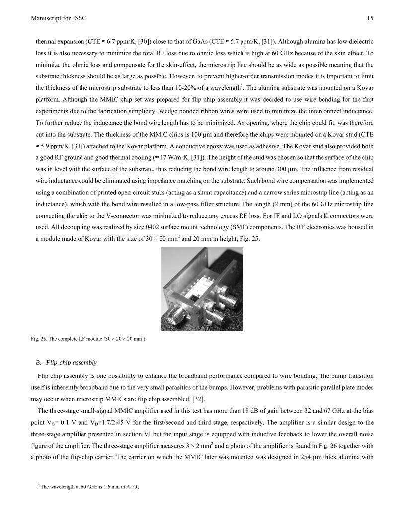
a module made of Kovar with the size of 30 × 20 mm2 and 20 mm in height, Fig. 25.
Fig. 25. The complete RF module (30 × 20 × 20 mm3).
B. Flip-chip assembly
Flip chip assembly is one possibility to enhance the broadband performance compared to wire bonding. The bump transition
itself is inherently broadband due to the very small parasitics of the bumps. However, problems with parasitic parallel plate modes
may occur when microstrip MMICs are flip chip assembled, [32].
The three-stage small-signal MMIC amplifier used in this test has more than 18 dB of gain between 32 and 67 GHz at the bias
point VG=-0.1 V and VD=1.7/2.45 V for the first/second and third stage, respectively. The amplifier is a similar design to the
three-stage amplifier presented in section VI but the input stage is equipped with inductive feedback to lower the overall noise
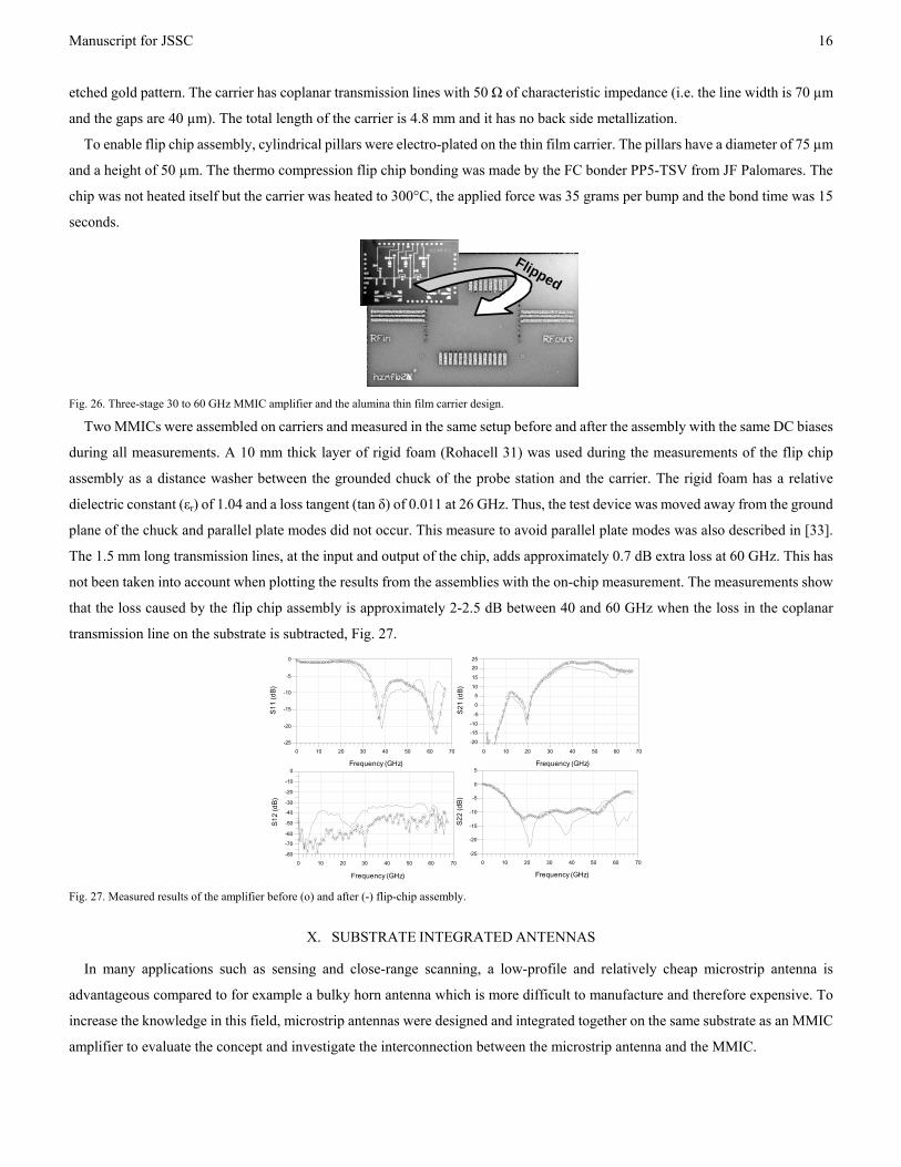
figure of the amplifier. The three-stage amplifier measures 3 × 2 mm2 and a photo of the amplifier is found in Fig. 26 together with
a photo of the flip-chip carrier. The carrier on which the MMIC later was mounted was designed in 254 µm thick alumina with
5 The wavelength at 60 GHz is 1.6 mm in Al2O3
Manuscript for JSSC
16
etched gold pattern. The carrier has coplanar transmission lines with 50 Ω of characteristic impedance (i.e. the line width is 70 µm
and the gaps are 40 µm). The total length of the carrier is 4.8 mm and it has no back side metallization.
To enable flip chip assembly, cylindrical pillars were electro-plated on the thin film carrier. The pillars have a diameter of 75 µm
and a height of 50 µm. The thermo compression flip chip bonding was made by the FC bonder PP5-TSV from JF Palomares. The
chip was not heated itself but the carrier was heated to 300°C, the applied force was 35 grams per bump and the bond time was 15
seconds.
Flipped
Fig. 26. Three-stage 30 to 60 GHz MMIC amplifier and the alumina thin film carrier design.
Two MMICs were assembled on carriers and measured in the same setup before and after the assembly with the same DC biases
during all measurements. A 10 mm thick layer of rigid foam (Rohacell 31) was used during the measurements of the flip chip
assembly as a distance washer between the grounded chuck of the probe station and the carrier. The rigid foam has a relative
dielectric constant (εr) of 1.04 and a loss tangent (tan δ) of 0.011 at 26 GHz. Thus, the test device was moved away from the ground
plane of the chuck and parallel plate modes did not occur. This measure to avoid parallel plate modes was also described in [33].
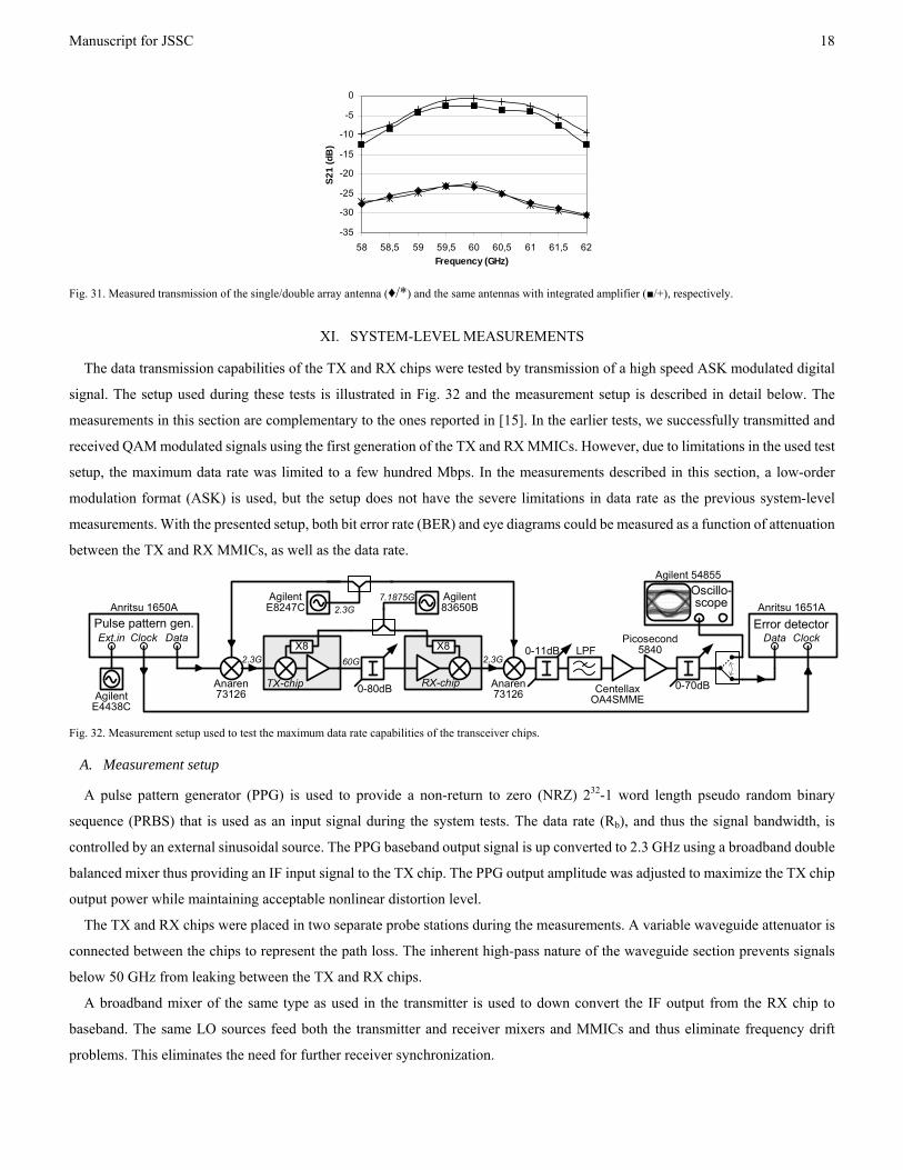
The 1.5 mm long transmission lines, at the input and output of the chip, adds approximately 0.7 dB extra loss at 60 GHz. This has
not been taken into account when plotting the results from the assemblies with the on-chip measurement. The measurements show
that the loss caused by the flip chip assembly is approximately 2-2.5 dB between 40 and 60 GHz when the loss in the coplanar
transmission line on the substrate is subtracted, Fig. 27.
10 20 30 40 50 600 70
-20
-15
-10
-5
-25
0
Frequency (GHz)
S1
1 (
dB
)
10 20 30 40 50 600 70
-15
-10
-5
0
5
10
15
20
-20
25
Frequency (GHz)
S2
1 (
dB
)
10 20 30 40 50 600 70
-70
-60
-50
-40
-30
-20
-10
-80
0
Frequency (GHz)
S1
2 (
dB
)
10 20 30 40 50 600 70
-20
-15
-10
-5
0
-25
5
Frequency (GHz)
S2
2 (
dB
)
Fig. 27. Measured results of the amplifier before (o) and after (-) flip-chip assembly.
X. SUBSTRATE INTEGRATED ANTENNAS
In many applications such as sensing and close-range scanning, a low-profile and relatively cheap microstrip antenna is
advantageous compared to for example a bulky horn antenna which is more difficult to manufacture and therefore expensive. To
increase the knowledge in this field, microstrip antennas were designed and integrated together on the same substrate as an MMIC
amplifier to evaluate the concept and investigate the interconnection between the microstrip antenna and the MMIC.

Manuscript for JSSC
17
Two types of microstrip patch antenna arrays were designed. One single array, Fig. 28, and one double array antenna, Fig. 29.
Array antennas were chosen to achieve a higher gain compared to single element antennas, and series feed networks were chosen
for simplicity and in order to avoid line intersections and impedance transformers. The single array antenna with eight patches
gives a beam that is wide in one plane and narrow in the other, with simulated beamwidths of 82° and 20°, respectively. The double
array antenna with two five-patch arrays connected in parallel is designed for equal beamwidths in both planes, with simulated
beamwidths of 33°. Both antennas have linear polarization, and sidelobe levels are below -11 dB relative to the beam peak. The
amplifier is a three-stage amplifier similar to the one presented in section VI and has a maximum gain of 20 dB and a 3 dB
bandwidth between 47 and 64 GHz. The antenna is etched on a 127 μm thick alumina substrate and the amplifier MMIC is placed
in a laser cut cavity in the substrate to enable short bond wires.
S-parameters of the antenna and MMIC amplifier were measured with a vector network analyzer (Agilent PNA). During the
measurements, one port of the network analyzer was connected to the probed input of the MMIC amplifier or directly to the
antenna. The other port was connected to the coaxial output of a sensing horn antenna as shown in Fig. 30. The results from the
measurements on the two antenna types with and without an MMIC amplifier are shown in Fig. 31. The amplifier increases the
transmission level by approximately 18 dB, which is in agreement with the measurements on the amplifier MMIC.
By this experiment, useful experience regarding building practice and antenna design was gained. The antennas can be used in
systems with more complex MMIC designs than the amplifier chip, e.g. such as the TX and RX MMICs presented in this paper. A
more detailed description of this work can be found in [34].
3 mm Fig. 28. Integrated single array antenna and MMIC amplifier.
3 mm
Fig. 29. Integrated double array antenna and MMIC amplifier.
Fig. 30. Sketch showing the setup for the antenna measurements. A GSG probe connects to the antenna port. A horn antenna is used to sense the radiation in the
broadside direction.
Manuscript for JSSC
18
-35
-30
-25
-20
-15
-10
-5
0
58 58,5 59 59,5 60 60,5 61 61,5 62Frequency (GHz)
S21
(dB
)
Fig. 31. Measured transmission of the single/double array antenna (♦/*) and the same antennas with integrated amplifier (/+), respectively.
XI. SYSTEM-LEVEL MEASUREMENTS
The data transmission capabilities of the TX and RX chips were tested by transmission of a high speed ASK modulated digital
signal. The setup used during these tests is illustrated in Fig. 32 and the measurement setup is described in detail below. The
measurements in this section are complementary to the ones reported in [15]. In the earlier tests, we successfully transmitted and
received QAM modulated signals using the first generation of the TX and RX MMICs. However, due to limitations in the used test
setup, the maximum data rate was limited to a few hundred Mbps. In the measurements described in this section, a low-order
modulation format (ASK) is used, but the setup does not have the severe limitations in data rate as the previous system-level
measurements. With the presented setup, both bit error rate (BER) and eye diagrams could be measured as a function of attenuation
between the TX and RX MMICs, as well as the data rate.
!
"
"
"
""
#$%%
""!
! !
&'
Fig. 32. Measurement setup used to test the maximum data rate capabilities of the transceiver chips.
A. Measurement setup
A pulse pattern generator (PPG) is used to provide a non-return to zero (NRZ) 232-1 word length pseudo random binary
sequence (PRBS) that is used as an input signal during the system tests. The data rate (Rb), and thus the signal bandwidth, is
controlled by an external sinusoidal source. The PPG baseband output signal is up converted to 2.3 GHz using a broadband double
balanced mixer thus providing an IF input signal to the TX chip. The PPG output amplitude was adjusted to maximize the TX chip
output power while maintaining acceptable nonlinear distortion level.
The TX and RX chips were placed in two separate probe stations during the measurements. A variable waveguide attenuator is
connected between the chips to represent the path loss. The inherent high-pass nature of the waveguide section prevents signals
below 50 GHz from leaking between the TX and RX chips.
A broadband mixer of the same type as used in the transmitter is used to down convert the IF output from the RX chip to
baseband. The same LO sources feed both the transmitter and receiver mixers and MMICs and thus eliminate frequency drift
problems. This eliminates the need for further receiver synchronization.

Manuscript for JSSC
19
A low-pass filter is used in the RX baseband chain to lower the noise floor and thus increase the measurement dynamic range.
Low-pass filters with different cutoff frequencies ranging from 600 MHz to 2.2 GHz were used depending on the Rb tested. Two
cascaded broadband amplifiers providing in total 40 dB gain were used to increase the signal level as needed for the error detector
(ED) instrument. The signal level was further controlled by two variable attenuators that simultaneously ensured that the amplifiers
operated in a linear regime and that the ED operated with signal amplitude suitable for proper symbol detection.
Although the ED is synchronized to the PPG by a separate clock connection, the time delay through the system needs to be
manually adjusted. This was done at each attenuator and Rb setting in order to obtain minimum BER results. The received signal
quality was visually investigated by displaying eye diagrams on an oscilloscope that could replace the ED at the end of the receiver
chain.
B. Measurement results and discussion
The setup described above allows convenient testing of BER as function of Rb and chip-to-chip attenuation. The attenuation
presented includes 11.4 dB total losses from cables, probes, and waveguide-to-coaxial transitions.
Fig. 33 shows BER versus attenuation for different Rb settings. The figure shows that 1.5 Gbps can be transmitted through 47 dB
attenuation with a raw BER = 10-3, which is a typical requirement in wireless systems before adding error correction techniques.
An idealized propagation calculation yields 88 dB free space path loss for 10 m transmission. Using directive antennas with
approximately 20 dB gain each, this means that the chips developed would allow wireless communication up to 10 m at 1.5 Gbps.
However, much larger distances would be possible in real system using antennas with even higher directivity, more correct IF
filtering, advanced modulation, and by introducing error correcting codes.
Fig. 33. Measured bit error rate (BER) versus chip-to-chip attenuation for different data rate settings.
The maximum data rate is further explored in Fig. 34, which shows BER vs. Rb for four attenuation settings. This plot clearly
shows that significantly higher data rates can be achieved if the path loss is decreased, either by using antennas with higher
directivity, external power amplifier on the TX side, or shorter distance.

Manuscript for JSSC
20
Fig. 34. Bit error rate (BER) versus data rate for different chip-to-chip attenuation.
The received signal quality is illustrated in Fig. 35, which shows eye diagrams for Rb ranging from 500 Mbps to 2.0 Gbps. Up to
1.5 Gbps, the eye opening is reasonably well defined, which indicates low probability of error as presented in previous plots. At 2.0
Gbps the eye has closed expressing the problem to communicate correctly at this data rate.
Fig. 35. Eye diagrams measured at the receiver for four different data rates
The test setup used is not well suited for evaluating wireless transmission using antennas since the chips are mounted in separate
probe stations and use common LO sources. Nevertheless, some tests using 60 GHz horn antennas were performed and verified
operation at 1.8 Gbps up to 0.5 m with BER < 10-3. The maximum distance was limited by the setup rather than the performance of
the chips.
The RX/TX chip have an IF bandwidth of > 1.8 GHz. The electrical 3 dB bandwidth typically needs to be at least 70% of Rb for
NRZ data, which would yield maximum Rb > 2.6 Gbps. However, in the present system Rb is probably limited by group delay
variations and receiver noise rather than the electrical bandwidth itself. For example, no external band-pass filter is used in front of
the RX chip, which significantly increases the receiver noise level and degrades the dynamic range. The external baseband-to-IF
mixers used have an electrical bandwidth of 1.5 GHz, which should also degrade the performance at high Rb, although they were
tested separately and allowed error free operation up to 2 Gbps. Further investigations will address performance limiting factors in
the presented TX and RX MMICs.
XII. SUMMARY AND DISCUSSION
The measured performance of the presented TX and RX chips are summarized in Tables V and VI, respectively. The default
values for RF, LO, and IF frequencies have been 60 GHz, 7.1875 GHz (giving 57.5 GHz output frequency from the X8), and 2.5
GHz, respectively.
TABLE V. SUMMARY OF MEASURED RESULTS FOR THE TX CHIP.
-1
1dB Input Comp. Point, dBm
-3
LO Power, dBm
420
PowerCons. (mW)
8 (56.5 – 64.5)
3 dB RF BW(rel. fC), GHz
1.8 (1.9 - 3.7)5.6
Output power (dBm)
ConversionGain, dB
3 dB IF BW(rel. fC), GHz
0.6

Manuscript for JSSC
21
TABLE VI. SUMMARY OF MEASURED RESULTS FOR THE RX CHIP.
ConversionGain, dB
1dB Input Comp. Point, dBm
-2
LO Power, dBm
450
PowerCons. (mW)
10 (54.5 – 64.5)
3 dB RF BW(rel. fC), GHz
1.9 (1.3 - 3.2)
3 dB IF BW*(rel. fC), GHz
> 13 (57.5 -67.5 GHz)
Image Rejection Ratio (dB)
-10
IIP3,dBm
7.0
NoiseFigure**, dB
*And a IRR of more than 10 dB, **Calculated value
12.9
-17
The presented TX and RX chips are true multipurpose 60 GHz front-end designs. During the measurements, the DC bias was
adjusted to find the optimal performance at 60 GHz in terms of output power for the TX chip and conversion gain for the RX chip.
Compared to the first generation of the designs, [15], the MMICs presented in this paper show the same high level of integration
but occupy smaller chip area and have higher gain and output power at only half of the DC power consumption. The reduction in
DC power consumption was obtained by optimizing the overall design with respect to DC power consumption, e.g. the number of
stages in the buffer amplifier used in the X8 LO chain was reduced from two to one stage compared with the pHEMT TX and RX
MMICs. Furthermore, the higher transconductance (gm) in the mHEMT compared to its pHEMT counterpart made it possible to
use lower drain biases (and hence reduced DC power consumption) in the former for the same mode of operation. Although not
integrated in the TX and RX MMICs, an mHEMT based VCO suitable for future integration was also presented. The VCO
possessed a wide tuning range and a phase noise good enough for many applications.
Although only a small number of chips have been measured, i.e. less than five TX and RX chips, no malfunctioning chips have
been found and the yield is therefore expected to be good.
Different packaging and interconnects issues were also presented. A description of the initial work on a module manufactured in
Kovar and equipped with coaxial connectors for output and input signals was shown. In this module, the TX and RX MMICs were
wire bonded to an alumina substrate, which is the conventional way of connecting an MMIC to the substrate. As an alternative to
wire bonding, experimental results of amplifiers mounted with flip-chip assembly technique were also presented. The flip-chip
interconnection added 2 – 2.5 dB of loss between 40 and 60 GHz compared to when the amplifiers were measured directly on-chip
with coplanar GSG probes. Furthermore, substrate integrated antennas for small, compact, and cheap transmitter and receiver
modules are also shown. The antennas are etched on a 127 μm thick alumina substrate and an amplifier MMIC is placed in a laser
cut cavity in the substrate and connected to the antenna with bond wires. Measurements with and without the amplifier mounted
demonstrated the usefulness of this technique.
Finally, system measurements are described where the presented TX and RX MMICs successfully transmitted and received a
modulated signal. The system measurements in this paper are complementary to the ones reported in [15]. In the earlier tests, we
successfully transmitted and received QAM modulated signals using the first version of the TX and RX MMICs. However, due to
limitations in the used test setup, the maximum data rate was limited to a few hundred Mbps. In the measurements described in this
paper, a low-order modulation format (ASK) is used, but the setup does not have the severe limitations in data rate as the
previously reported system-level measurements. Plots of bit error rate (BER) versus attenuation between the TX and RX MMICs
together with eye diagrams have demonstrated that the presented TX and RX MMICs support data rates beyond 1.5 Gbps, even
when using very simple ASK modulation. Using higher order modulation (e.g. QPSK or some kind of QAM modulation having
higher bandwidth efficiency), more correct IF filtering, and by introducing error correcting codes the maximum data rate could be
extended even further.
Manuscript for JSSC
22
XIII. CONCLUSIONS
60 GHz MMIC transmitter and receiver chips, designed in an mHEMT technology, have been simulated, manufactured, and
experimentally verified. The single chip transmitter MMIC consists of a balanced resistive mixer with an integrated ultra
broadband IF balun, a three-stage post amplifier, and a multiply-by-eight (X8) LO chain. The single chip receiver MMIC has an
equally high level of integration with a three-stage low noise amplifier, an image reject mixer with an integrated ultra broadband IF
hybrid and the same X8 LO chain as used in the transmitter chip. Although not integrated in the TX and RX MMICs, an mHEMT
based VCO suitable for future integration was also presented.
Packaging and interconnects are discussed and a module where the TX and RX MMICs are wire bonded to an alumina substrate
is presented. As an alternative to wire bonding, flip-chip assembly tests were also presented and discussed. The results of those
tests clearly showed the suitability of flip-chip as a broadband interconnecting technique for MMICs. Substrate integrated antennas
for small, compact, and low-cost transmitter and receiver modules were also successfully demonstrated and verified by
measurements.
The system-level measurements of BER and eye diagrams have demonstrated that the presented TX and RX MMICs support
data rates beyond 1.5 Gbps, even using a simple ASK modulation. Using higher order modulation (e.g. QPSK or QAM), more
correct IF filtering, and by introducing error correcting codes the maximum data rate could be extended even further.
ACKNOWLEDGMENT
Thomas Lewin at Ericsson AB and Jan Grahn at Chalmers University of Technology are acknowledged for their shown interest
in this work. Niklas Wadefalk at Chalmers University of Technology is acknowledged for support of the noise figure
measurements. The Taiwanese foundry WIN is acknowledged for a fruitful co-operation.
REFERENCES
[1] A.J. Richardson and P.A. Watson, “Use of the 55-65 GHz oxygen absorption band fort short-range broadband radio networks with minimal regulatory
control”, IEE Proceedings, Vol.137, Part I, pp. 233-241, August 1990
[2] Peter Smulders, “Exploiting the 60 GHz Band for Local Wireless Multimedia Access: Prospects and Future Directions”, IEEE Communications Magazine,
pp.140-147, January 2002
[3] C. Fager, S. Gunnarsson, A. Alping, and U. Engström, ”Systems and Applications for Broadband Wireless Communication in the 60 GHz Band”, Proceedings
of GigaHertz 2005 conference, Uppsala, Sweden, pp. 28-31, 8-9 November 2005
[4] F.J. Velez and M. Dinis, “Mobile Broadband Systems: Research and Visions”, IEEE Vehicular Technology Society News, vol. 52, no. 2, pp. 4-12, May 2005
[5] M. de Courville, S. Zeisberg, M. Muck, and J. Schönthier, “BROADWAY – the Way to Broadband Access at 60 GHz”, IST Mobile & Wireless
Telecommunications Summit, Thessaloniki, Greece, June 2002 and http:/www.ist-broadway.org (as of 8 February 2006)
[6] K. Hamaguchi, Y. Shoji, H. Ogawa, H. Sato, T. Tokuda, Y. Hirachi, T. Iwasaki, A. Akeyama, K. Ueki, and T. Kizawa, “A Wireless Video Home-Link using
60 GHz Band: Concept and Performance of the Developed System”, Proceedings of the 30th European Microwave Conference 2000, Vol. 1, pp. 293-296,
Paris, 2-6 October 2000
[7] M. Siddiqui, M. Ouije, A. Lawrence, B. Pitman, R. Katz, P. Tran, A. Chau, D. Davidson, S. Din, R. Lai, and D. Streit, “GaAs Components for 60 GHz Wireless
Communication applications”, Technical Digest of GaAs Mantech Conference, San Diego, CA, USA, 11 April, 2002
[8] K. Fujii, M. Adamski, P. Bianco, D. Gunyan, J. Hall, R. Kishimura, C. Lesko, M. Schefer, S. Hessel, H. Morkner, and A. Niedzwiecki, “A 60 GHz MMIC
Chipset for 1-Gbit/s Wireless Links”, Proceedings of IEEE MTT-S International Microwave Symposium 2002, pp. 1725 1728, Seattle, Washington, USA, 2-7
June 2002
[9] O. Vaudescal, B. Lefebvre, V. Lehoué, and P. Quentin, “A Highly Integrated MMIC Chipset for 60 GHz Broadband Wireless Applications”, Proceedings of
IEEE MTT-S International Microwave Symposium 2002, vol. 3, pp. 1729-1732, Seattle, Washington, USA, 2-7 June 2002
[10] Y. Mimino, K. Nakamura, Y. Hasegawea, Y. Aoki, S. Kuroda, and T. Tokumitsu, “A 60 GHz Millimeter-wave MMIC chipset for Broadband Wireless Access
System Front-end”, Proceedings of IEEE MTT-S International Microwave Symposium 2002, vol. 3, pp. 1721-1724, Seattle, Washington, USA, 2-7 June 2002

Manuscript for JSSC
23
[11] K. Ohata, K. Maruhashi, M. Ito, S. Kishimoto, K. Ikuina, T. Hashiguchi, K. Ikeda, and N. Takahashi, “1.25 Gbps Wireless Gigabit Ethernet Link at 60
GHz-Band”, Proceedings of IEEE Radio Frequency Integrated Circuits Symposium (RFIC) 2003, pp. 509-512, Philadelphia, PA, USA, 8-10 June 2003
[12] H. Zirath, T. Masuda, R. Kozhuharov, and M. Ferndahl, “Development of 60 GHz Front-End Circuits for a High-Data-Rate Communication System”, IEEE J.
of Solid-State Circuits, vol. 39, no. 10, pp. 1640-1649, October 2004
[13] B. Floyd, S. Reynolds, U. Pfeiffer, T. Beukema, J. Grzyb, C. Haymes, “A Silicon 60 GHz Receiver and Transmitter Chipset for Broadband Communications”,
Proceedings of IEEE International Solid-State Circuits Conference, ISSCC 2006, pp. 184 – 185, San Francisco, CA, USA, 5-9 February 2006
[14] C. H. Doan, S. Emami, D. A. Sobel, A. M. Niknejad, and R. W. Brodersen, “Design Considerations for 60 GHz CMOS Radios”, IEEE Communications
Magazine, vol. 42, no. 12, pp. 132-140, December 2004
[15] S. E. Gunnarsson, C. Kärnfelt, H. Zirath, R. Kozhuharov, D. Kuylenstierna, A. Alping, and C. Fager, “Highly Integrated 60 GHz Transmitter and Receiver
MMICs in a GaAs pHEMT Technology”, IEEE Journal of Solid-State Circuits, vol. 40, no. 11, pp. 2174-2186, November 2005
[16] S. E. Gunnarsson, C. Kärnfelt, H. Zirath, R. Kozhuharov, D. Kuylenstierna, A. Alping, and C. Fager, “Single-Chip 60 GHz Transmitter and Receiver MMICs
in a GaAs mHEMT Technology”, Proceedings of IEEE MTT-S International Microwave Symposium 2006, San Francisco, California, USA, 11-16, pp.
801-804, June 2006
[17] D. Kuylenstierna, S. E. Gunnarsson, and H. Zirath, “Lumped element quadrature power splitters using mixed right/left-handed transmission lines”, IEEE
Trans. Microwave Theory Tech., vol. 53, no. 8, pp. 2616-2621, Aug. 2005.
[18] B. S. Virdee, A. S. Virdee, and B. Y. Banyamin, “Broadband Microwave Amplifiers”, Artech House, 2004.
[19] G. Dambrine, A. Cappy, F. Heliodore., and E. Playez, “A New Method for Determining the FET Small-Signal Equivalent Circuit”, IEEE Trans. Microwave
Theory Tech., vol. 36, no. 7, pp. 1151-1159, July 1988.
[20] H. Zirath, C. Fager, M. Garcia, P. Sakalas, L. Landen, and A. Alping, “Analog MMICs for Millimeter-Wave Applications Based on a Commercial 0.14-μm
pHEMT Technology” IEEE Trans. Microwave Theory Tech., vol. 49, no. 11, pp. 2086-2092, November 2001.
[21] D. Y. Jung, W. I. Chang, and C. S. Park, “A System-on-Package Integration of 60 GHz Transmitter”, Proceedings of IEEE Radio and wireless symposium
(RWS) 2006, San Diego, CA, USA, 17-19 January 2006
[22] J. Mizoe, S. Amano, T. Kuwabara, T. Kaneko, K. Wada, A. Kato, K. Sato, and M. Fujise, “Miniature 60 GHz Transmitter/Receiver Modules on IIN
Multi-Layer High Temperature Co-Fired Ceramic,” Digest of IEEE MTT-S conference 1999, pp. 475-478, Anaheim, CA, USA, 13-19 June 1999
[23] J. Grzyb, I. Ruiz, D. Cottet, and G. Tröster, ”An Investigation of the Material and Process Parameters for Thin-Film MCM-D and MCM-L Technologies up to
100 GHz,” Proc. of 53rd ECTC, pp. 478-486, New Orleans, Louisiana, USA, 27-30 May 2003
[24] W. Heinrich, “The Flip-Chip Approach for Millimeter-Wave Packaging”, IEEE Microwave Magazine, vol. 6, no. 3, pp. 36-45, September 2005.
[25] C. Kärnfelt, R. Kozhuharov, H. Zirath, and I. Angelov, “High Purity 60 GHz-Band Single Chip X8 Multiplier in pHEMT and mHEMT technology”, IEEE
Trans. Microwave Theory Tech., vol. 54, no. 6, Part 2, pp. 2887-2898, June 2006.
[26] H. Zirath, R. Kozhuharov, and M. Ferndahl, “Balanced colpitt oscillator mmics designed for ultra-low phase noise,” IEEE Journal of Solid-State Circuits, vol.
40, no. 10, pp. 2077–2086, 2005.
[27] J. Portilla, M. L. de la Fuente, J. P. Pascual, and E. Artal, “Low-noise monolithic Ku-band VCO using pseudomorphic HEMT technology,” IEEE Microwave
and Guided Wave Letters, vol. 7, no. 11, pp. 380–2, 1997.
[28] M. Ferndahl, H. Zirath, “Broadband 7 GHz VCO in mHEMT Technology”, Proceedings of the IEEE Asia Pacific Microwave Conference 2005, APMC2005,
2005.
[29] D. Kuylenstierna and P. Linnér, “Design of broad-band lumped-element baluns with inherent impedance transformation”, IEEE Trans. Microwave Theory
Tech., vol. 52, no. 12, pp. 2739-2745, Dec. 2004.
[30] American Technical Ceramics (ATC), “ATC Custom Thin Film Products”, ATC # 001-824 Rev. D, 1/04
[31] J. A. King (Ed.), “Materials Handbook for Hybrid Microelectronics”. pp. 470, Norwood, MA, Artech House, 1988
[32] W. Heinrich, A. Jentsch and G. Baumann, Millimeter-Wave Characteristics of Flip-Chip Interconnects for Multichip Modules, IEEE Trans. Microwave
Theory Tech., vol. 46, no. 12, pp. 2264-2268, Dec. 1998.
[33] C. Kärnfelt, C. Tegnander, J. Rudnicki, J. P. Starski, and A. Emrich, ”Investigation of Parylene-C on the performance of mm-wave circuits”, to be published in
IEEE Trans. of Microwave Theory Tech., August, 2006.
[34] C. Kärnfelt, P. Hallbjörner, H. Zirath, and A. Alping, “High Gain Active Microstrip Antenna for 60 GHz WLAN/WPAN Applications”, IEEE Trans.
Microwave Theory Tech., vol. 54, no. 6, Part 2, pp. 2593-2603, June 2006.
Manuscript for JSSC
24
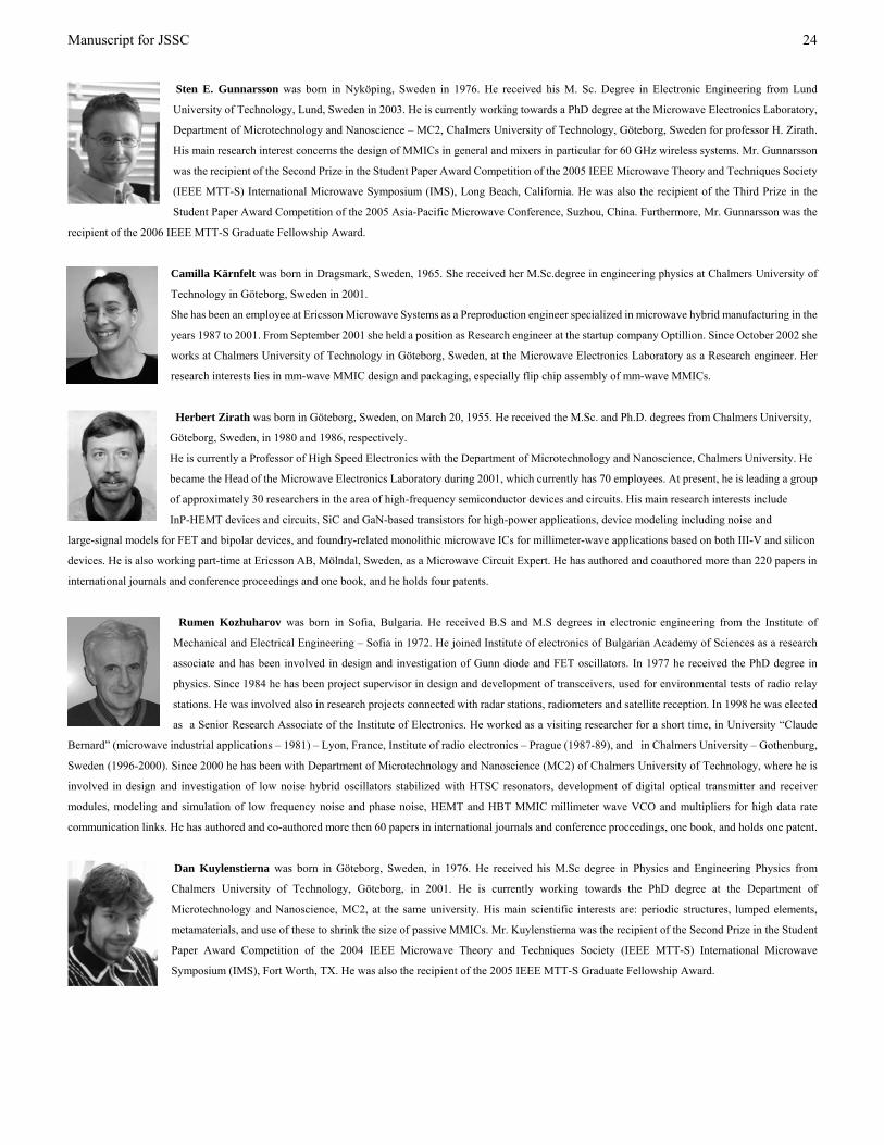
Sten E. Gunnarsson was born in Nyköping, Sweden in 1976. He received his M. Sc. Degree in Electronic Engineering from Lund
University of Technology, Lund, Sweden in 2003. He is currently working towards a PhD degree at the Microwave Electronics Laboratory,
Department of Microtechnology and Nanoscience – MC2, Chalmers University of Technology, Göteborg, Sweden for professor H. Zirath.
His main research interest concerns the design of MMICs in general and mixers in particular for 60 GHz wireless systems. Mr. Gunnarsson
was the recipient of the Second Prize in the Student Paper Award Competition of the 2005 IEEE Microwave Theory and Techniques Society
(IEEE MTT-S) International Microwave Symposium (IMS), Long Beach, California. He was also the recipient of the Third Prize in the
Student Paper Award Competition of the 2005 Asia-Pacific Microwave Conference, Suzhou, China. Furthermore, Mr. Gunnarsson was the
recipient of the 2006 IEEE MTT-S Graduate Fellowship Award.
Camilla Kärnfelt was born in Dragsmark, Sweden, 1965. She received her M.Sc.degree in engineering physics at Chalmers University of
Technology in Göteborg, Sweden in 2001.
She has been an employee at Ericsson Microwave Systems as a Preproduction engineer specialized in microwave hybrid manufacturing in the
years 1987 to 2001. From September 2001 she held a position as Research engineer at the startup company Optillion. Since October 2002 she
works at Chalmers University of Technology in Göteborg, Sweden, at the Microwave Electronics Laboratory as a Research engineer. Her
research interests lies in mm-wave MMIC design and packaging, especially flip chip assembly of mm-wave MMICs.
Herbert Zirath was born in Göteborg, Sweden, on March 20, 1955. He received the M.Sc. and Ph.D. degrees from Chalmers University,
Göteborg, Sweden, in 1980 and 1986, respectively.
He is currently a Professor of High Speed Electronics with the Department of Microtechnology and Nanoscience, Chalmers University. He
became the Head of the Microwave Electronics Laboratory during 2001, which currently has 70 employees. At present, he is leading a group
of approximately 30 researchers in the area of high-frequency semiconductor devices and circuits. His main research interests include
InP-HEMT devices and circuits, SiC and GaN-based transistors for high-power applications, device modeling including noise and
large-signal models for FET and bipolar devices, and foundry-related monolithic microwave ICs for millimeter-wave applications based on both III-V and silicon
devices. He is also working part-time at Ericsson AB, Mölndal, Sweden, as a Microwave Circuit Expert. He has authored and coauthored more than 220 papers in
international journals and conference proceedings and one book, and he holds four patents.
Rumen Kozhuharov was born in Sofia, Bulgaria. He received B.S and M.S degrees in electronic engineering from the Institute of
Mechanical and Electrical Engineering – Sofia in 1972. He joined Institute of electronics of Bulgarian Academy of Sciences as a research
associate and has been involved in design and investigation of Gunn diode and FET oscillators. In 1977 he received the PhD degree in
physics. Since 1984 he has been project supervisor in design and development of transceivers, used for environmental tests of radio relay
stations. He was involved also in research projects connected with radar stations, radiometers and satellite reception. In 1998 he was elected
as a Senior Research Associate of the Institute of Electronics. He worked as a visiting researcher for a short time, in University “Claude
Bernard” (microwave industrial applications – 1981) – Lyon, France, Institute of radio electronics – Prague (1987-89), and in Chalmers University – Gothenburg,
Sweden (1996-2000). Since 2000 he has been with Department of Microtechnology and Nanoscience (MC2) of Chalmers University of Technology, where he is
involved in design and investigation of low noise hybrid oscillators stabilized with HTSC resonators, development of digital optical transmitter and receiver
modules, modeling and simulation of low frequency noise and phase noise, HEMT and HBT MMIC millimeter wave VCO and multipliers for high data rate
communication links. He has authored and co-authored more then 60 papers in international journals and conference proceedings, one book, and holds one patent.
Dan Kuylenstierna was born in Göteborg, Sweden, in 1976. He received his M.Sc degree in Physics and Engineering Physics from
Chalmers University of Technology, Göteborg, in 2001. He is currently working towards the PhD degree at the Department of
Microtechnology and Nanoscience, MC2, at the same university. His main scientific interests are: periodic structures, lumped elements,
metamaterials, and use of these to shrink the size of passive MMICs. Mr. Kuylenstierna was the recipient of the Second Prize in the Student
Paper Award Competition of the 2004 IEEE Microwave Theory and Techniques Society (IEEE MTT-S) International Microwave
Symposium (IMS), Fort Worth, TX. He was also the recipient of the 2005 IEEE MTT-S Graduate Fellowship Award.

Manuscript for JSSC
25
Christian Fager was born in Varberg, Sweden, 1974. He received the M.Sc. and Ph.D. degrees in electrical engineering and microwave
electronics, from Chalmers University of Technology, Göteborg, Sweden, in 1998 and 2003, respectively. Currently he is working as an
Assistant Professor at the Microwave Electronics Laboratory.
His research interests are in the areas of large signal transistor modeling and nonlinear circuit design. Dr. Fager received the Best Student
Paper Award at the IEEE International Microwave Symposium in 2002.
Mattias Ferndahl was born in Stockholm, Sweden, in 1973. He received the M.Sc. degree in Physics Engineering from Chalmers University
of Technology, Göteborg, Sweden, where he is currently working as a Ph.D. student at the department of Microtechnology and Nanoscience,
Microwave Electronics lab. His research interests are mainly low noise VCOs and CMOS for micro and millimeter wave applications.
Bertil Hansson was born in Vänersborg, Sweden, in 1945. He received the M. Sc. Degree in electrical engineering and the Ph. D. degree in
solid-state electronics from the Chalmers University of Technology, Göteborg, Sweden, in 1970 and 1973, respectively.
In 1974, he was a consultant for Ericsson and in 1975 he joined Ericsson Microwave Systems, Mölndal, Sweden. Since 1988, he has been
involved in the design of application specified integrated circuits (ASICs) and, in 1991, he joined a group designing ASICs for optical
communication links for Ericsson Telecom. In 1996, he joined the Corporate Research Centre for Microwave and High Speed Electronics,
Ericsson Microwave Systems as a Senior Research Engineer. His research interest was SiGe and GaAs monolithic microwave integrated
circuits (MMICs) for microwave communications in the frequency range from 5 to 100 GHz. Since 2004, he is a Research Engineer with Microwave Electronics
Laboratory, Chalmers University of Technology, Göteborg, Sweden, working with design of GaAs MMICs.
Arne Alping was born in Finspong, Sweden, in 1953. He received the MSEE and PhD degrees from the Chalmers University of Technology,
Göteborg, in 1979 and 1984, respectively.
From 1980 to 1985 he was working at the Department of Optoelectronics at Chalmers, where his research included gigabit-rate fiber-optic
communication systems, and different aspects of the laser diode as a multi-functional device. In 1985 he joined the research staff at UCSB,
Santa Barbara, CA, USA, and spent one year conducting research on cleaved-coupled-cavity lasers and high efficiency waveguide optical
phase modulators. He returned to Chalmers in 1986, where his research was concerned with noise and coherence properties of laser diodes,
external cavity lasers, and high-speed waveguide photodiodes.
Since 1988 he is at Ericsson, Mölndal, Sweden, where he is working on broadband interconnects. For several years he was engaged in work on fiber-optic data
links for aerospace and radar applications. From 1997 he is at the Microwave and High Speed Electronics Research Center (MHSERC), Ericsson Research, where
he is involved in high-speed fiber-optic digital links, optical interconnects and RF/microwave photonics for wireless communication systems. His work also
includes high-speed interconnect technologies for PCB and backplanes, wireless sensor networks, as well as broadband wireless (60 GHz) systems. He is author and
co-author to over 60 publications in international journals and conference proceedings in the areas of photonics, mm wave electronics, and packaging &
interconnects.
Paul Hallbjörner was born in Uppsala, Sweden, in 1966. He received his B.Sc. (1988), M.Sc. (1995), and Ph.D. (2005) degrees in electrical
engineering from Chalmers University of Technology, Göteborg, Sweden. His technical experience is mainly in the field of antennas and
microwave technology, but he also has experience in electronics design and testing. He has been working in the telecom industry since 1989,
and since 2000 as a researcher with focus on antennas and measurement techniques. He is currently with the SP Swedish National Testing and
Research Institute. He is the author and co-author of more than 40 scientific publications, on antennas, antenna measurement techniques,
reverberation chamber techniques, and microwave design and analysis. He is also the inventor to several patents in microwave technology
and wireless communication.
Per Ligander was born in Göteborg, Sweden, 1951. He has been working at Ericsson, Mölndal, Sweden since 1974. From 1996 he is
working as a Senior Research engineer at the Microwave and High Speed Research Center (MHSERC), Ericsson Research, where he is
involved in microwave building practice, such as packaging & Interconnects and Printed circuit board. He is author and co-author to a
number of publications in international journals and conference proceedings in the area of microwave building practice. He holds more than
30 patens.
View publication statsView publication stats


![2.4 GHz Single-chip Preliminary - Digi-Key Sheets/Atmel PDFs...I_CPSW RAMP D/A 2.4 GHz WDECT/ISM Single-chip Transceiver T2803 Preliminary 2 T2803 [Preliminary] 4572G–DECT–01/04](https://img.dokumen.tips/doc/110x75/5b0d5d197f8b9a6a6b8dc37f/24-ghz-single-chip-preliminary-digi-key-sheetsatmel-pdfsicpsw-ramp-da-24.jpg)