Embed Size (px)
Citation preview
3/16/2011 section 5_6 Small Signal Operation and Models 1/2
Jim Stiles The Univ. of Kansas Dept. of EECS
5.6 Small-Signal Operation and Models
Reading Assignment: 443-458
Now let’s examine how we use BJTs to construct amplifiers! The first important design rule is that the BJT must be biased to the active mode.
HO: BJT GAIN AND THE ACTIVE REGION For a BJT amplifier, we find that every current and every voltage has two components: the DC (i.e., bias) component—a value carefully selected and designed by a EE, and the small-signal component, which is the AC signal we are attempting to amplify (e.g., audio, video, etc.).
HO:DC AND SMALL-SIGNAL COMPONENTS There are two extremely important circuit elements in small-signal amplifier design: the Capacitor of Unusual Size (COUS) and the Inductor of Unusual Size (IOUS). These devices are just realizable approximations of the Unfathomably Large Capacitor (ULC) and the Unfathomably Large Inductor (ULI). These devices have radically different properties when considering DC and small-signal components!
HO:DC AND AC IMPEDANCE OF REACTIVE ELEMENTS
3/16/2011 section 5_6 Small Signal Operation and Models 2/2
Jim Stiles The Univ. of Kansas Dept. of EECS
It turns out that separating BJT currents and voltages into DC and small-signal components is problematic!
HO:THE SMALL-SIGNAL CIRCUIT EQUATIONS But, we can approximately determine the small-signal components if we use the small-signal approximation.
HO: A SMALL-SIGNAL ANALYSIS OF HUMAN GROWTH
HO: A SMALL-SIGNAL ANALYSIS OF A BJT Let’s do an example to illustrate the small-signal approximation.
EXAMPLE: SMALL-SIGNAL BJT APPROXIMATIONS There are several small-signal parameters that can be extracted from a small-signal analysis of a BJT.
HO: BJT SMALL-SIGNAL PARAMETERS
HO: THE SMALL-SIGNAL EQUATION MATRIX Let’s do an example!
EXAMPLE: CALCULATING THE SMALL-SIGNAL GAIN
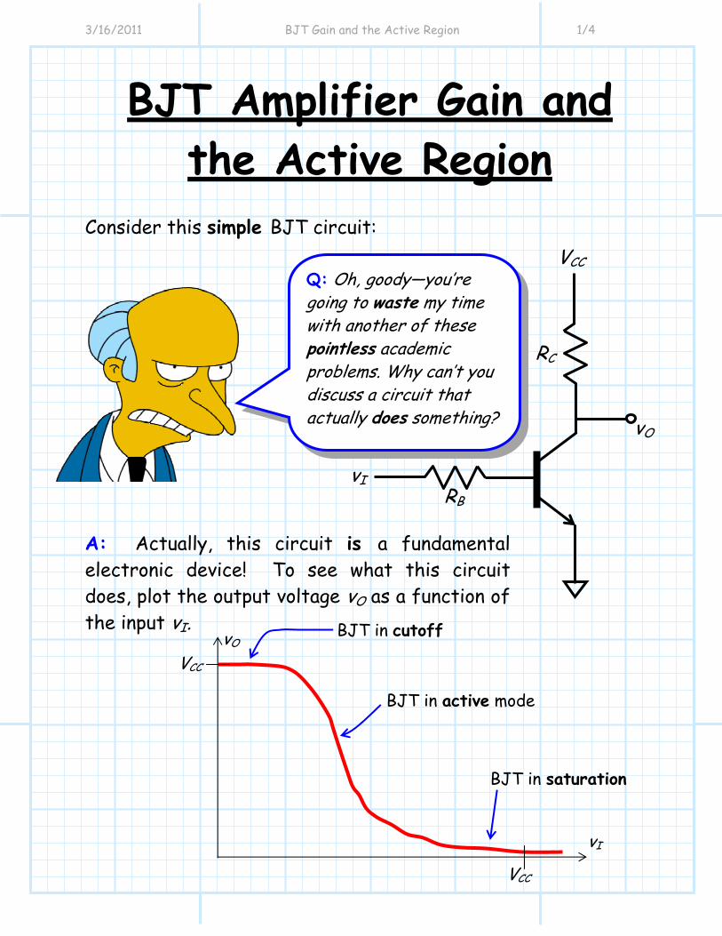
3/16/2011 BJT Gain and the Active Region 1/4
BJT Amplifier Gain and the Active Region
Consider this simple BJT circuit: A: Actually, this circuit is a fundamental electronic device! To see what this circuit does, plot the output voltage vO as a function of the input vI.
Q: Oh, goody—you’re going to waste my time with another of these pointless academic problems. Why can’t you discuss a circuit that actually does something?
RC
vI RB
VCC
vO
vO
vI
VCC
VCC
BJT in cutoff
BJT in active mode
BJT in saturation

3/16/2011 BJT Gain and the Active Region 2/4
Note that:
Digital devices made with BJTs typically work in either the cutoff of saturation regions.
vI vO Mode 0 VCC Cutoff VCC 0 Saturation
Sir, it appears to me that the active region is just a useless BJT mode between cutoff and saturation.
So, what good is the BJT Active Mode ??
Why, this device is not useless at all! It is clearly a: ____________________
3/16/2011 BJT Gain and the Active Region 3/4
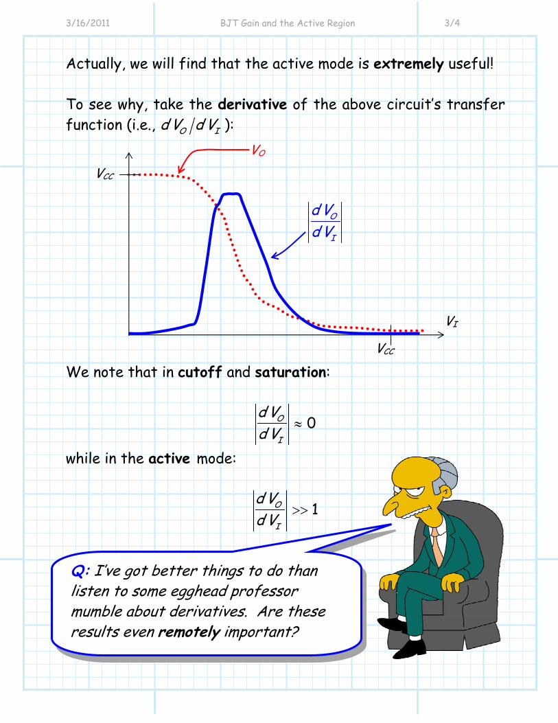
Actually, we will find that the active mode is extremely useful! To see why, take the derivative of the above circuit’s transfer function (i.e., O Id V d V ): We note that in cutoff and saturation:
0O
I
d Vd V ≈
while in the active mode:
1O
I
d Vd V >>
VO
VI
VCC
VCC
O
I
d Vd V
Q: I’ve got better things to do than listen to some egghead professor mumble about derivatives. Are these results even remotely important?

3/16/2011 BJT Gain and the Active Region 4/4
A: Since in cutoff and saturation 0O Id V d V = , a small change in input voltage VI will result in almost no change in output voltage VO . Contrast this with the active region, where 1O Id V d V >> . This means that a small change in input voltage VI results in a large change in the output voltageVO ! Whereas the important BJT regions for digital devices are saturation and cutoff, bipolar junction transistors in linear (i.e., analog) devices are typically biased to the active region. This is especially true for BJT amplifier. Almost all of the transistors in EECS 412 will be in the active region—this is where we get amplifier gain !
I see. A small voltage change results in a big voltage change—it’s voltage gain! The active mode turns out to be—excellent.
3/16/2011 DC and Small Signal Components 1/5
Jim Stiles The Univ. of Kansas Dept. of EECS
DC and Small-Signal Components
Note that we have used DC sources in all of our example circuits thus far. We have done this just to simplify the analysis—generally speaking, realistic (i.e., useful) junction diode circuits will have sources that are time-varying! The result will be voltages and currents in the circuit that will likewise vary with time (e.g., ( )i t and ( )v t ). For example, we can express the forward bias junction diode equation as:
( )( )D
T
v tnV
D si t I e= Although source voltages ( )Sv t or currents ( )Si t can be any general function of time, we will find that often, in realistic and useful electronic circuits, that the source can be decomposed into two separate components—the DC component SV , and the small-signal component ( )sv t . I.E.:
) )( (S sS vV tv t = +
3/16/2011 DC and Small Signal Components 2/5
Jim Stiles The Univ. of Kansas Dept. of EECS
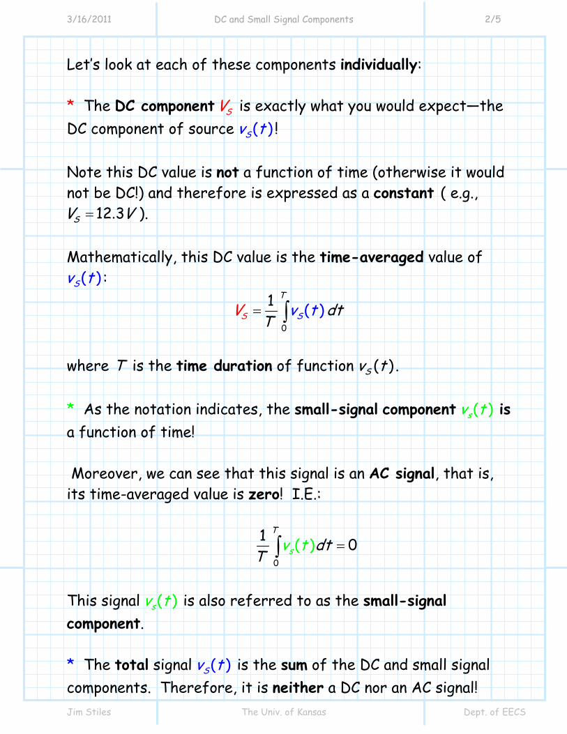
Let’s look at each of these components individually: * The DC component SV is exactly what you would expect—the DC component of source ( )Sv t ! Note this DC value is not a function of time (otherwise it would not be DC!) and therefore is expressed as a constant ( e.g.,
.12 3SV V= ). Mathematically, this DC value is the time-averaged value of
( )Sv t :
0
( )1 T
S Sv t dtT
V = ∫
where T is the time duration of function ( )Sv t .
* As the notation indicates, the small-signal component ( )sv t is a function of time! Moreover, we can see that this signal is an AC signal, that is, its time-averaged value is zero! I.E.:
0
1 0( )T
s dtv tT
=∫
This signal ( )sv t is also referred to as the small-signal component. * The total signal ( )Sv t is the sum of the DC and small signal components. Therefore, it is neither a DC nor an AC signal!
3/16/2011 DC and Small Signal Components 3/5
Jim Stiles The Univ. of Kansas Dept. of EECS
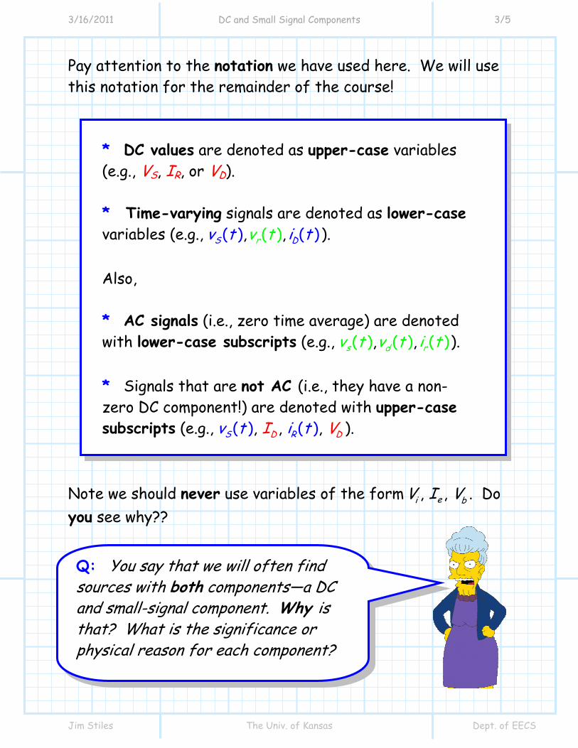
Pay attention to the notation we have used here. We will use this notation for the remainder of the course!
* DC values are denoted as upper-case variables (e.g., VS, IR, or VD). * Time-varying signals are denoted as lower-case variables (e.g., (( ) ( ), ,)S Drv tv t i t ). Also, * AC signals (i.e., zero time average) are denoted with lower-case subscripts (e.g., ( ) ( ) (, ),s rdv t v t i t ). * Signals that are not AC (i.e., they have a non-zero DC component!) are denoted with upper-case subscripts (e.g., ( ) (, ) , ,S RD Dv t i tI V ).
Note we should never use variables of the form , , ei bV I V . Do you see why??
Q: You say that we will often find sources with both components—a DC and small-signal component. Why is that? What is the significance or physical reason for each component?
3/16/2011 DC and Small Signal Components 4/5
Jim Stiles The Univ. of Kansas Dept. of EECS
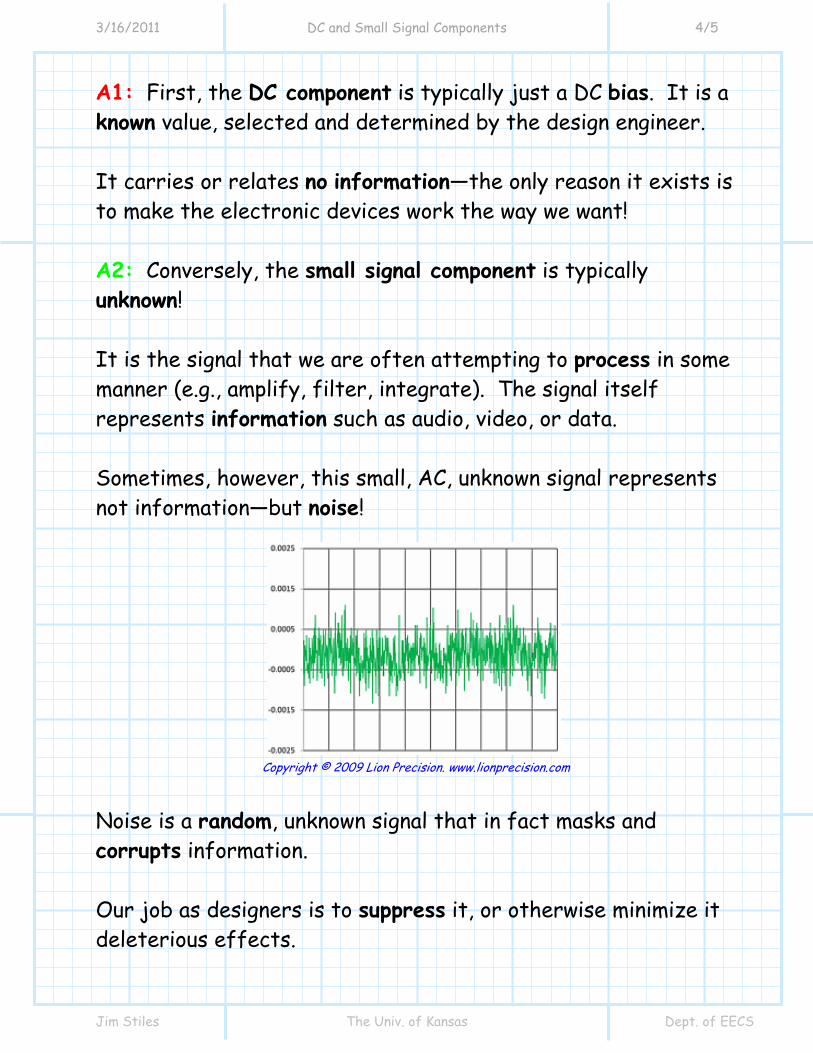
A1: First, the DC component is typically just a DC bias. It is a known value, selected and determined by the design engineer. It carries or relates no information—the only reason it exists is to make the electronic devices work the way we want! A2: Conversely, the small signal component is typically unknown! It is the signal that we are often attempting to process in some manner (e.g., amplify, filter, integrate). The signal itself represents information such as audio, video, or data. Sometimes, however, this small, AC, unknown signal represents not information—but noise!
Copyright © 2009 Lion Precision. www.lionprecision.com
Noise is a random, unknown signal that in fact masks and corrupts information. Our job as designers is to suppress it, or otherwise minimize it deleterious effects.
3/16/2011 DC and Small Signal Components 5/5
Jim Stiles The Univ. of Kansas Dept. of EECS
* This noise may be changing very rapidly with time (e.g., MHz), or may be changing very slowly (e.g., mHz). * Rapidly changing noise is generally “thermal noise”, whereas slowly varying noise is typically due to slowly varying environmental conditions, such as temperature.
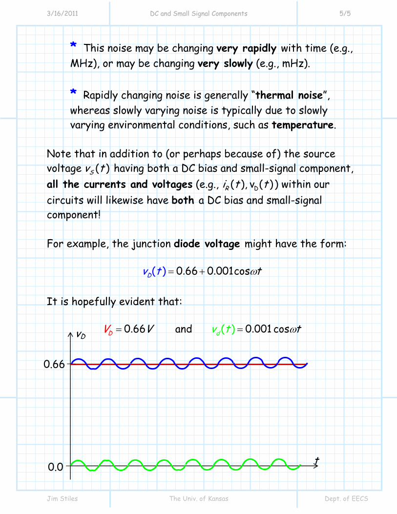
Note that in addition to (or perhaps because of) the source voltage ( )Sv t having both a DC bias and small-signal component, all the currents and voltages (e.g., D( ), v ( )Ri t t ) within our circuits will likewise have both a DC bias and small-signal component! For example, the junction diode voltage might have the form:
. .0 66 0 001co( ) sDv tt ω= +
It is hopefully evident that:
. .( )0 66 and 0 001 cosdD v t tV V= = ω
0.66
vD
t 0.0
3/16/2011 DC and AC Impedance of Reactive Elements 1/6
Jim Stiles The Univ. of Kansas Dept. of EECS
DC and AC Impedance of Reactive Elements
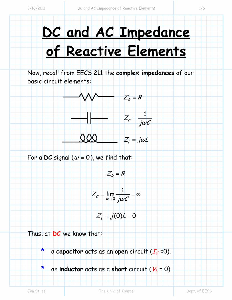
Now, recall from EECS 211 the complex impedances of our basic circuit elements:
RZ R=
1CZ
jωC=
LZ jωL=
For a DC signal ( 0ω = ), we find that:
RZ R=
0
1limC ωZ
jωC→= = ∞
(0) 0LZ j L= =
Thus, at DC we know that:
* a capacitor acts as an open circuit (IC =0). * an inductor acts as a short circuit (VL = 0).

3/16/2011 DC and AC Impedance of Reactive Elements 2/6
Jim Stiles The Univ. of Kansas Dept. of EECS
Now, let’s consider two important cases: 1. A capacitor whose capacitance C is unfathomably
large. 2. An inductor whose inductance L is unfathomably
large. 1. The Unfathomably Large Capacitor In this case, we consider a capacitor whose capacitance is finite, but very, very, very large. For DC signals ( 0ω = ), this device acts still acts like an open circuit. However, now consider the AC signal case (e.g., a small signal), where 0ω ≠ . The impedance of an unfathomably large capacitor is:
1lim 0C CZ
jωC→∞= =
Zero impedance!
An unfathomably large capacitor acts like an AC short.
3/16/2011 DC and AC Impedance of Reactive Elements 3/6
Jim Stiles The Univ. of Kansas Dept. of EECS
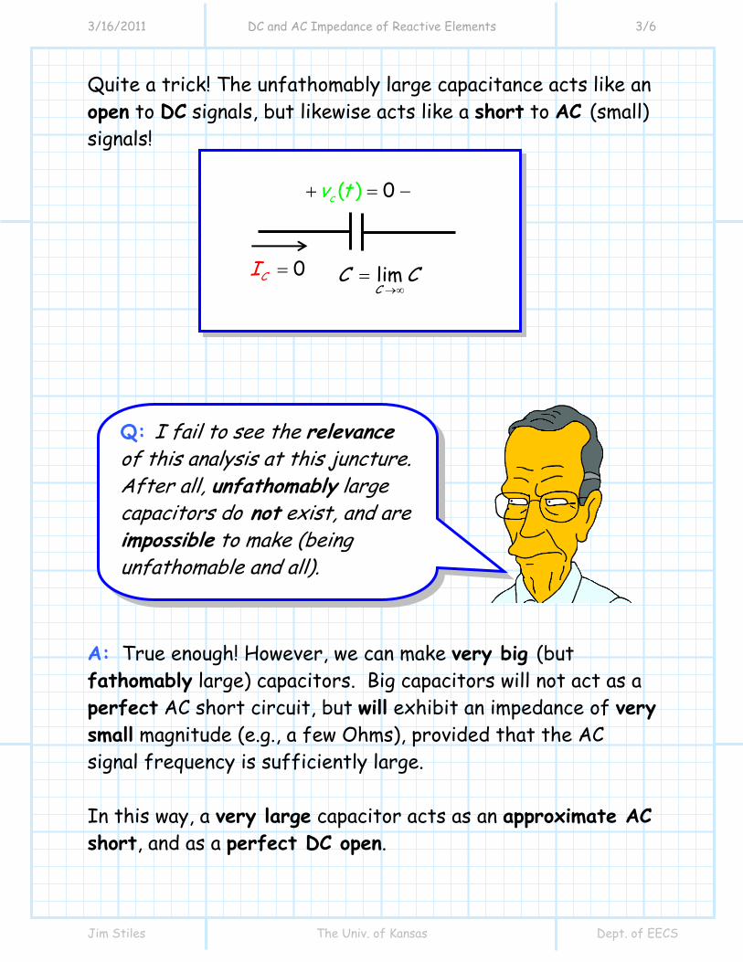
Quite a trick! The unfathomably large capacitance acts like an open to DC signals, but likewise acts like a short to AC (small) signals! A: True enough! However, we can make very big (but fathomably large) capacitors. Big capacitors will not act as a perfect AC short circuit, but will exhibit an impedance of very small magnitude (e.g., a few Ohms), provided that the AC signal frequency is sufficiently large. In this way, a very large capacitor acts as an approximate AC short, and as a perfect DC open.
0CI =
) 0(cv t+ = −
limC
C C→∞
=
Q: I fail to see the relevance of this analysis at this juncture. After all, unfathomably large capacitors do not exist, and are impossible to make (being unfathomable and all).
3/16/2011 DC and AC Impedance of Reactive Elements 4/6
Jim Stiles The Univ. of Kansas Dept. of EECS
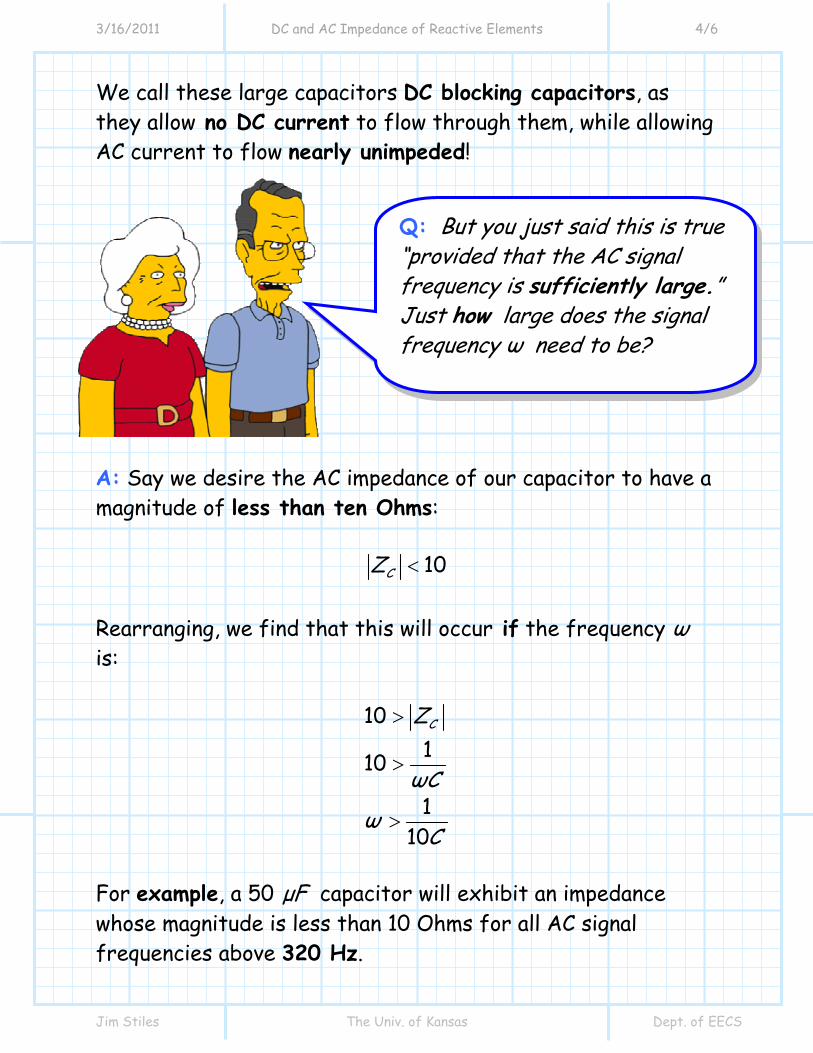
We call these large capacitors DC blocking capacitors, as they allow no DC current to flow through them, while allowing AC current to flow nearly unimpeded! A: Say we desire the AC impedance of our capacitor to have a magnitude of less than ten Ohms:
10CZ <
Rearranging, we find that this will occur if the frequency ω is:
10110
110
CZ
ωC
ωC
>
>
>
For example, a 50 µF capacitor will exhibit an impedance whose magnitude is less than 10 Ohms for all AC signal frequencies above 320 Hz.
Q: But you just said this is true “provided that the AC signal frequency is sufficiently large.” Just how large does the signal frequency ω need to be?
3/16/2011 DC and AC Impedance of Reactive Elements 5/6
Jim Stiles The Univ. of Kansas Dept. of EECS
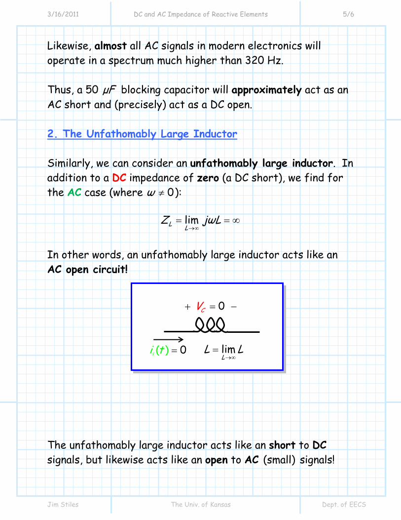
Likewise, almost all AC signals in modern electronics will operate in a spectrum much higher than 320 Hz. Thus, a 50 µF blocking capacitor will approximately act as an AC short and (precisely) act as a DC open. 2. The Unfathomably Large Inductor Similarly, we can consider an unfathomably large inductor. In addition to a DC impedance of zero (a DC short), we find for the AC case (where 0ω ≠ ):
limL LZ jωL
→∞= = ∞
In other words, an unfathomably large inductor acts like an AC open circuit! The unfathomably large inductor acts like an short to DC signals, but likewise acts like an open to AC (small) signals!
0CV+ = −
) 0(i t = limL
L L→∞
=
3/16/2011 DC and AC Impedance of Reactive Elements 6/6
Jim Stiles The Univ. of Kansas Dept. of EECS
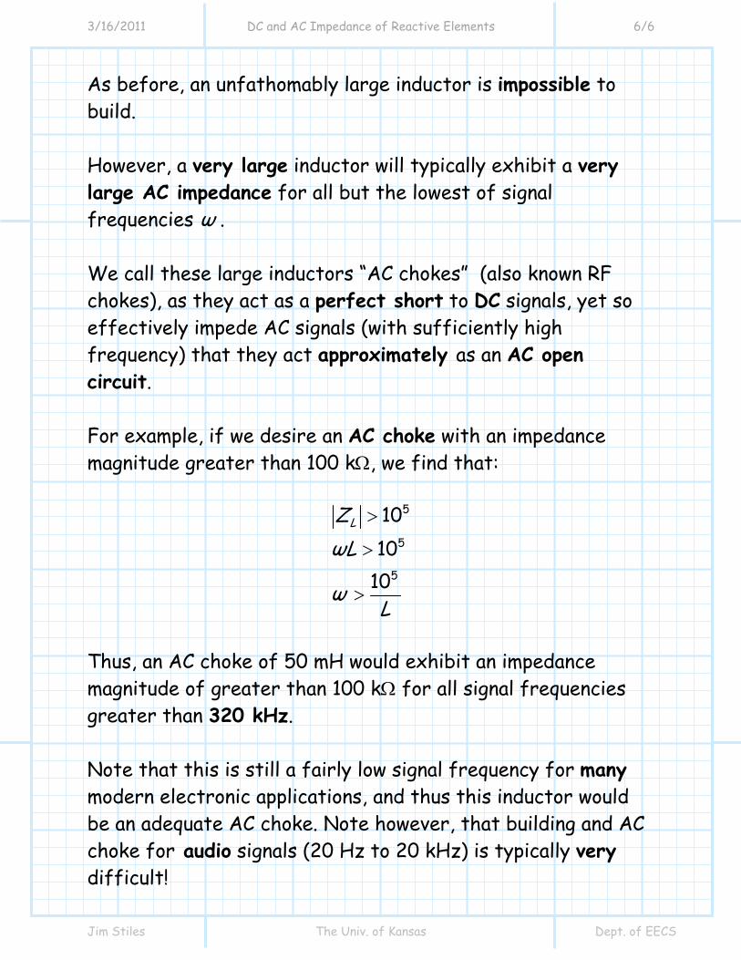
As before, an unfathomably large inductor is impossible to build. However, a very large inductor will typically exhibit a very large AC impedance for all but the lowest of signal frequencies ω . We call these large inductors “AC chokes” (also known RF chokes), as they act as a perfect short to DC signals, yet so effectively impede AC signals (with sufficiently high frequency) that they act approximately as an AC open circuit. For example, if we desire an AC choke with an impedance magnitude greater than 100 kΩ, we find that:
5
5
5
1010
10
LZωL
ωL
>
>
>
Thus, an AC choke of 50 mH would exhibit an impedance magnitude of greater than 100 kΩ for all signal frequencies greater than 320 kHz. Note that this is still a fairly low signal frequency for many modern electronic applications, and thus this inductor would be an adequate AC choke. Note however, that building and AC choke for audio signals (20 Hz to 20 kHz) is typically very difficult!

3/28/2011 The Small Signal Circuit Equations 1/4
The Small-Signal Circuit Equations
Now let’s again consider this circuit, where we assume the BJT is in the active mode: The four equations describing this circuit are:
1) 0I B B BEv R i v− − = (KVL) 2) BCi iβ= (BJT) 3) O CC C Cv V R i= − (KVL)
4) BE
T
vV
sCi I e= (BJT)
RC
Iv RB
VCC
Ci
Bi
Ov
BEv+
−

3/28/2011 The Small Signal Circuit Equations 2/4
Now, we assume that each current and voltage has both a small-signal and DC component. Writing each equation explicitly in terms of these components, we find that the four circuit equations become:
(1) ( ) ( ) ( ) 0 ( ) ( ) 0
I i B B b beBE
I B B i B b beBE
V v R I i V vV R I V v R i v
+ − + − + =
− − + − − =
(2) ( )C c B b
C c B b
I i I iI i I i
ββ β
+ = +
+ = +
(3) ( )
( )O o CC C C c
O o CC C C C c
V v V R I iV v V R I R i
+ = − +
+ = − −
( )
(4) beBE
T
BE beT T
V vV
C c sV v
V VC c s
I i I e
I i I e e
+
+ =
+ =
Note that each equation is really two equations! 1. The sum of the DC components on one side of the equal sign must equal the sum of the DC components on the other. 2. The sum of the small-signal components on one side of the equal sign must equal the sum of the small-signal components on the other. This result can greatly simplify our quest to determine the small-signal amplifier parameters!

3/28/2011 The Small Signal Circuit Equations 3/4
From (1) we find that the DC equation is:
0I B B BEV R I V− − =
while the small-signal equation from 1) is:
0i B b bev R i v− − =
Similarly, from equation (2) we get these equations:
BCI Iβ= (DC)
c bi iβ= (small signal)
And from equation (3):
O CC C CV V R I= − (DC)
o cCv R i= (small-signal)
You see, all we need to do is determine four small-signal equations, and we can then solve for the four small-signal values
, , , c ob bei i v v !
3/28/2011 The Small Signal Circuit Equations 4/4
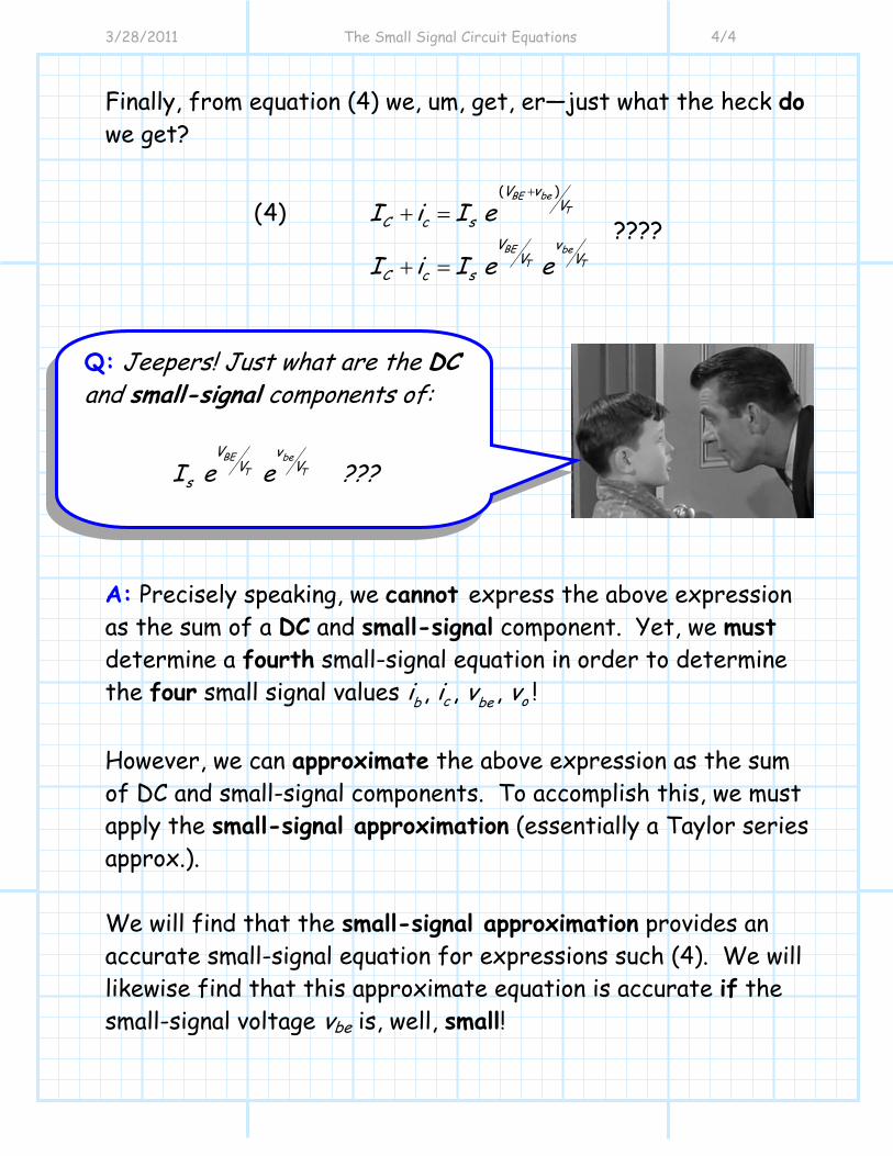
Finally, from equation (4) we, um, get, er—just what the heck do we get?
( )
(4) beBE
T
BE beT T
V vV
C c sV v
V VC c s
I i I e
I i I e e
+
+ =
+ = ????
A: Precisely speaking, we cannot express the above expression as the sum of a DC and small-signal component. Yet, we must determine a fourth small-signal equation in order to determine the four small signal values , , , c ob bei i v v ! However, we can approximate the above expression as the sum of DC and small-signal components. To accomplish this, we must apply the small-signal approximation (essentially a Taylor series approx.). We will find that the small-signal approximation provides an accurate small-signal equation for expressions such (4). We will likewise find that this approximate equation is accurate if the small-signal voltage vbe is, well, small!
Q: Jeepers! Just what are the DC and small-signal components of:
BE be
T T
V vV V
sI e e ???
3/16/2011 A Small-Signal Analysis of Human Growth 1/6
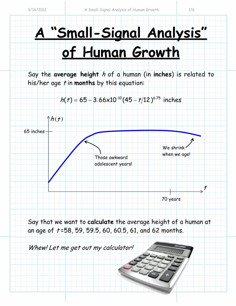
A “Small-Signal Analysis” of Human Growth
Say the average height h of a human (in inches) is related to his/her age t in months by this equation:
-10 6.75( ) 65 3 66x10 (45 12) inches.h t t= − −
Say that we want to calculate the average height of a human at an age of t =58, 59, 59.5, 60, 60.5, 61, and 62 months. Whew! Let me get out my calculator!
( )h t
t
Those awkward adolescent years!
We shrink when we age!
70 years
65 inches
3/16/2011 A Small-Signal Analysis of Human Growth 2/6
( 58 0) 40 48 inches( 59 0) 40 82 inches( 59 5) 40 99 inches( 60 0) 41 16 inches( 60 5) 41 32 inches( 61 0) 41 49 inches( 62 0) 41 82 inches
. .
. .
. .
. .
. .. .. .
h th th th th th th t
= =
= =
= =
= =
= =
= =
= =
Q: Wow, this was hard. Isn’t there an easier way to calculate these values? A: Yes, there is! We can make a “small-signal” approximation. For a small-signal approximation, we simply need to calculate two values. First:
60 ( 60) 41 16 inches( ) .t h th t == = =
In other words, the average height of a human at 60 months (i.e., 5 years) is 41.16 inches. Likewise, we calculate the time derivative of ( )h t , and then evaluate the result at 60 months:
( )-10 5.7560
60-10 5.75
( ) 2 059 x10 (45 12)
2 059 x10 (45 60 12)0 34 inches/month
.
.
.
tt
d h t tdt =
=
= −
= −
=

3/16/2011 A Small-Signal Analysis of Human Growth 3/6
In other words, the average 5 year old grows at a rate of 0.34 inches/month! Now let’s again consider the earlier problem. If we know that an average 5-year old is 41.16 inches tall, and grows at a rate of 0.34 inches/month, then at 5 years and one month (i.e., 61 months), the little bugger will approximately be:
41 16 (0.34)(1) 41 50 inches. .+ =
Compare this to the exact value of 41.49 inches—a very accurate approximation. We can likewise approximate the average height of a 59-month old (i.e., 5 years minus one month):
41 16 (0.34)( 1) 40 83 inches. .+ − =
or of a 62-month old (i.e., 5 years plus two months):
41 16 (0.34)(2) 41 83 inches. .+ = Note again the accuracy of these approximations! For this approximation, let us define time t =60 as the evaluation point, or bias point T :
evaluation pointT

3/16/2011 A Small-Signal Analysis of Human Growth 4/6
We can then define: t t T∆ = −
In this example then, T = 60 months, and the values of t∆ range from –2 to +2 months. For example, t = 59 months can be expressed as t T t= + ∆ , where 60 monthsT = and 1t∆ = − month. We can therefore write our approximation as:
( )( )( )t T
t T
d h th th t tdt=
=
≈ + ∆
For the example where T =60 months we find:
6060
( )( ) ( )
41 16 0 34
tt
d h th t th tdt
t
==
≈ + ∆
= + ∆. .
This approximation is not accurate, however, if t∆ is large. For example, we can determine from the exact equation that the average height of a forty-year old human is:
( 480) 65 inchesh t = =
or about 5 feet 5 inches.

3/16/2011 A Small-Signal Analysis of Human Growth 5/6
However, if we were to use our approximation to determine the average height of a 40-year old ( 480 60 420t t T∆ = − = − = ), we would find:
( ) 41 16 0 34 (420)181 86 inches
. ..
h t ≈ +
=
The approximation says that the average 40-year old human is over 15 feet tall! The reason that the above approximation provides an inaccurate answer is because it is based on the assumption that humans grow at a rate of 0.34 inches/month. This is true for 5-year olds, but not for 40-year olds (unless, of course, you are referring to their waistlines)! We thus refer to the approximation function as a “small-signal” approximation, as it is valid only for times that are slightly different from the nominal (evaluation) time T (i.e., t∆ is small).
Where exactly do I find these dad-gum humans?

3/16/2011 A Small-Signal Analysis of Human Growth 6/6
If we wish to have an approximate function for the growth of humans who are near the age of forty, we would need to construct a new approximation:
480480
6
( )( ) ( )
65 0 2 2 x 10
tt
d h th t th tdt
t
==
−
≈ + ∆
= + ∆. .
Note that forty-year old humans have stopped growing! The mathematically astute will recognize the small-signal model as a first-order Taylor Series approximation!

3/28/2011 A Small Signal Analysis of a BJT lecture 1/12
Jim Stiles The Univ. of Kansas Dept. of EECS
A Small-Signal Analysis of a BJT
The collector current Ci of a BJT is related to its base-emitter voltage BEv as:
Ci
BEv
BET
vV
SCi I e=
3/28/2011 A Small Signal Analysis of a BJT lecture 2/12
Jim Stiles The Univ. of Kansas Dept. of EECS
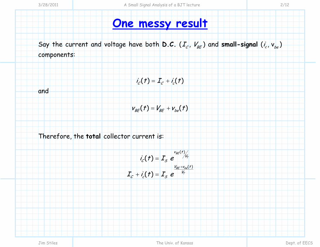
One messy result Say the current and voltage have both D.C. ( , C BEI V ) and small-signal ( , vc bei ) components:
( ) ( )C C ci t I i t= + and
( ) ( )BE BE bev t V v t= +
Therefore, the total collector current is:
( )
( )
( )
( )
BET
BE be
T
v tV
C SV v t
VC c S
i t I e
I i t I e+
=
+ =
3/28/2011 A Small Signal Analysis of a BJT lecture 3/12
Jim Stiles The Univ. of Kansas Dept. of EECS
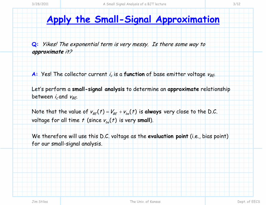
Apply the Small-Signal Approximation Q: Yikes! The exponential term is very messy. Is there some way to approximate it? A: Yes! The collector current ic is a function of base emitter voltage vBE. Let’s perform a small-signal analysis to determine an approximate relationship between ic and vBE. Note that the value of ( ) ( )BE BE bev t V v t= + is always very close to the D.C. voltage for all time t (since ( )bev t is very small). We therefore will use this D.C. voltage as the evaluation point (i.e., bias point) for our small-signal analysis.
3/28/2011 A Small Signal Analysis of a BJT lecture 4/12
Jim Stiles The Univ. of Kansas Dept. of EECS
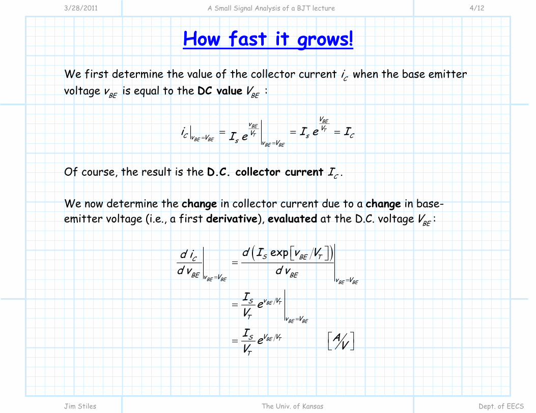
How fast it grows! We first determine the value of the collector current Ci when the base emitter voltage BEv is equal to the DC value BEV :
BEBE
TT
BE BEBE BE
Vv VVC s Cv V s v V
i I e II e==
= = =
Of course, the result is the D.C. collector current CI . We now determine the change in collector current due to a change in base-emitter voltage (i.e., a first derivative), evaluated at the D.C. voltage BEV :
( )exp
BE BE BE BE
TBE
BE BE
TBE
S TBEC
BE BEv V v V
v VS
T v V
V VS
T
d I v Vd id v d v
I eV
I Ae VV
= =
=
⎡ ⎤⎣ ⎦=
=
⎡ ⎤= ⎣ ⎦
3/28/2011 A Small Signal Analysis of a BJT lecture 5/12
Jim Stiles The Univ. of Kansas Dept. of EECS
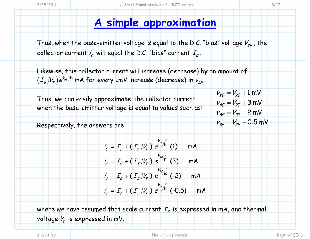
A simple approximation Thus, when the base-emitter voltage is equal to the D.C. “bias” voltage BEV , the collector current Ci will equal the D.C. “bias” current CI . Likewise, this collector current will increase (decrease) by an amount of ( ) TBEV V
S TI V e mA for every 1mV increase (decrease) in BEv . Thus, we can easily approximate the collector current when the base-emitter voltage is equal to values such as: Respectively, the answers are:
( ) (1) mA
( ) (3) mA
( ) (-2) mA
( ) (-0.5) mA
BET
BET
BET
BET
VV
SC C TV
VSC C T
VV
SC C TV
VSC C T
i I I V e
i I I V e
i I I V e
i I I V e
= +
= +
= +
= +
where we have assumed that scale current SI is expressed in mA, and thermal voltage TV is expressed in mV.
1 mV3 mV2 mV0 5 mV
BE BE
BE BE
BE BE
BE BE
v Vv Vv Vv V
= += += −= − .
3/28/2011 A Small Signal Analysis of a BJT lecture 6/12
Jim Stiles The Univ. of Kansas Dept. of EECS
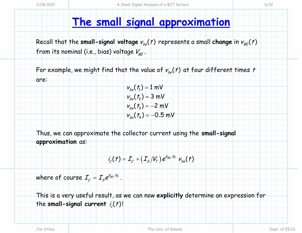
The small signal approximation Recall that the small-signal voltage ( )bev t represents a small change in ( )BEv t from its nominal (i.e., bias) voltage BEV . For example, we might find that the value of ( )bev t at four different times t are:
1
2
3
4
( ) 1 mV( ) 3 mV( ) 2 mV( ) 0 5 mV
be
be
be
be
v tv tv tv t
=== −= − .
Thus, we can approximate the collector current using the small-signal approximation as:
( )( ) ( )BE TV VC C S T bei t I I V e v t= +
where of course TBEV V
SCI I e= . This is a very useful result, as we can now explicitly determine an expression for the small-signal current ( )ci t !

3/28/2011 A Small Signal Analysis of a BJT lecture 7/12
Jim Stiles The Univ. of Kansas Dept. of EECS
The small-signal collector current Recall ( ) ( )C C ci t I i t= + , therefore:
( )( ) ( ) ( )BE TV VC C c C S T bei t I i t I I V e v t= + = +
Subtracting the D.C. current from each side, we are left with an expression for the small-signal current ( )ci t , in terms of the small-signal voltage ( )bev t :
( )( ) ( )BE TV Vc S T bei t I V e v t=
We can simplify this expression by noting that TBEV V
SCI I e= , resulting in:
( )TBE
TBE
V VV V S
S TT
C
T
I eI V eV
IV
=
=
and thus:
( ) ( )Cc be
T
Ii t v tV
=
3/28/2011 A Small Signal Analysis of a BJT lecture 8/12
Jim Stiles The Univ. of Kansas Dept. of EECS
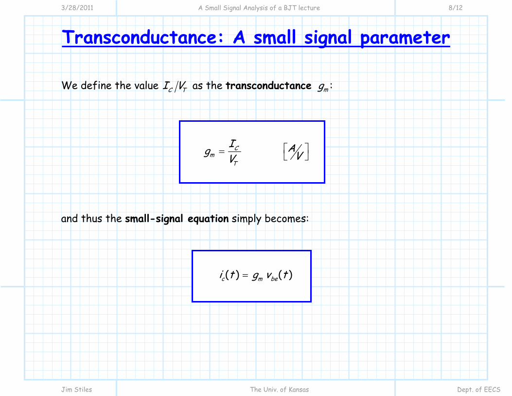
Transconductance: A small signal parameter We define the value C TI V as the transconductance mg :
C
mT
I Ag VV⎡ ⎤= ⎣ ⎦
and thus the small-signal equation simply becomes:
( ) ( )c m bei t g v t=

3/28/2011 A Small Signal Analysis of a BJT lecture 9/12
Jim Stiles The Univ. of Kansas Dept. of EECS
How transistors got their name Let’s now consider for a moment the transconductance mg . The term is short for transfer conductance: conductance because its units are amps/volt, and transfer because it relates the collector current to the voltage from base to emitter—the collector voltage is not relevant (if in active mode)!
Note we can rewrite the small-signal equation as:
( ) 1( )
be
c m
v ti t g
=
The value (1 )mg can thus be considered as transfer resistance, the value describing a transfer resistor. Transfer Resistor—we can shorten this term to Transistor (this is how these devices were named)!
3/28/2011 A Small Signal Analysis of a BJT lecture 10/12
Jim Stiles The Univ. of Kansas Dept. of EECS
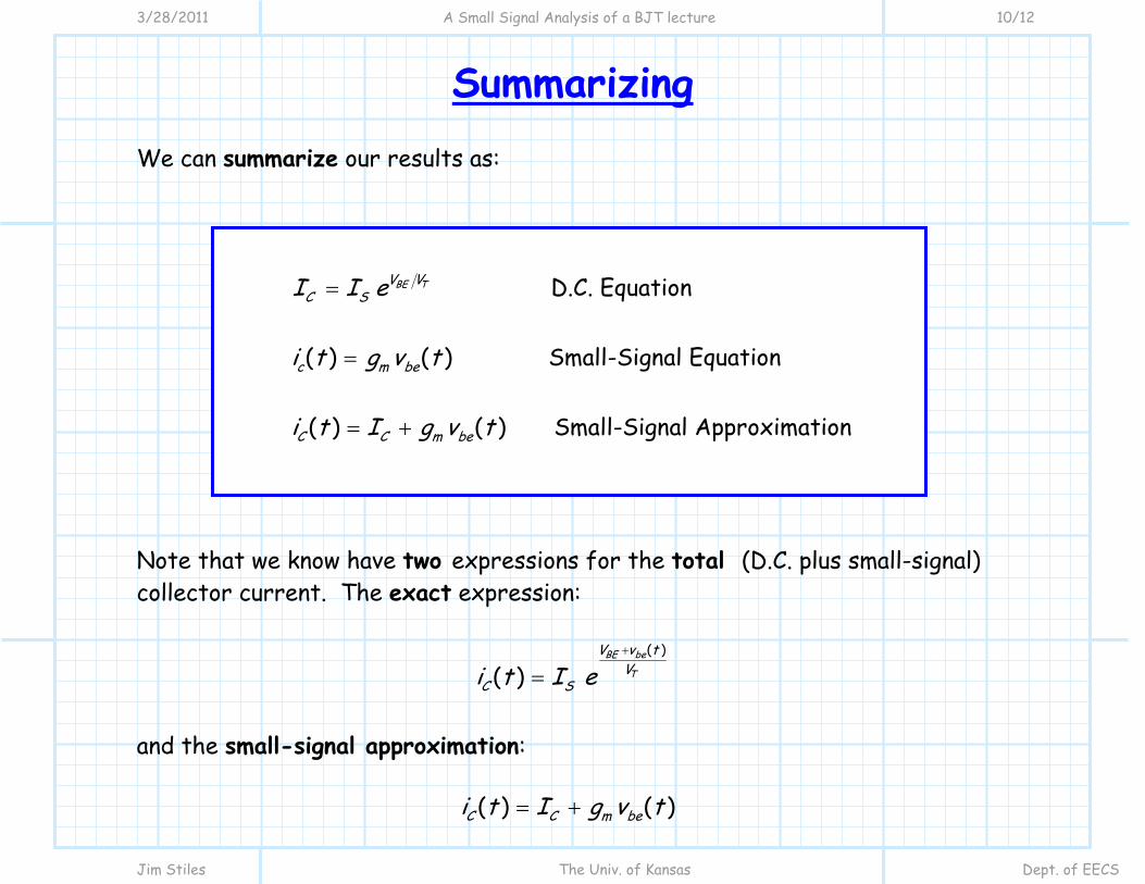
Summarizing We can summarize our results as:
D.C. Equation
( ) ( ) Small-Signal Equation
( ) ( ) Small-Signal Approximation
BE TV VC S
c m be
C C m be
I I e
i t g v t
i t I g v t
=
=
= +
Note that we know have two expressions for the total (D.C. plus small-signal) collector current. The exact expression:
( )
( )BE be
T
V v tV
C Si t I e+
=
and the small-signal approximation:
( ) ( ) C C m bei t I g v t= +

3/28/2011 A Small Signal Analysis of a BJT lecture 11/12
Jim Stiles The Univ. of Kansas Dept. of EECS
Accurate over a small region Let’s plot these two expressions and see how they compare:
It is evident that the small-signal approximation is accurate (it provides nearly the exact values) only for values of iC near the D.C bias value IC , and only for values of vC near the D.C bias value VC. The point ( , CBEV I ) is alternately known as the D.C. bias point, the transistor operating point, or the Q-point.
Ci
BEv
BEV
CI
mg
Exact Small-signal Validity Regions
3/28/2011 A Small Signal Analysis of a BJT lecture 12/12
Jim Stiles The Univ. of Kansas Dept. of EECS
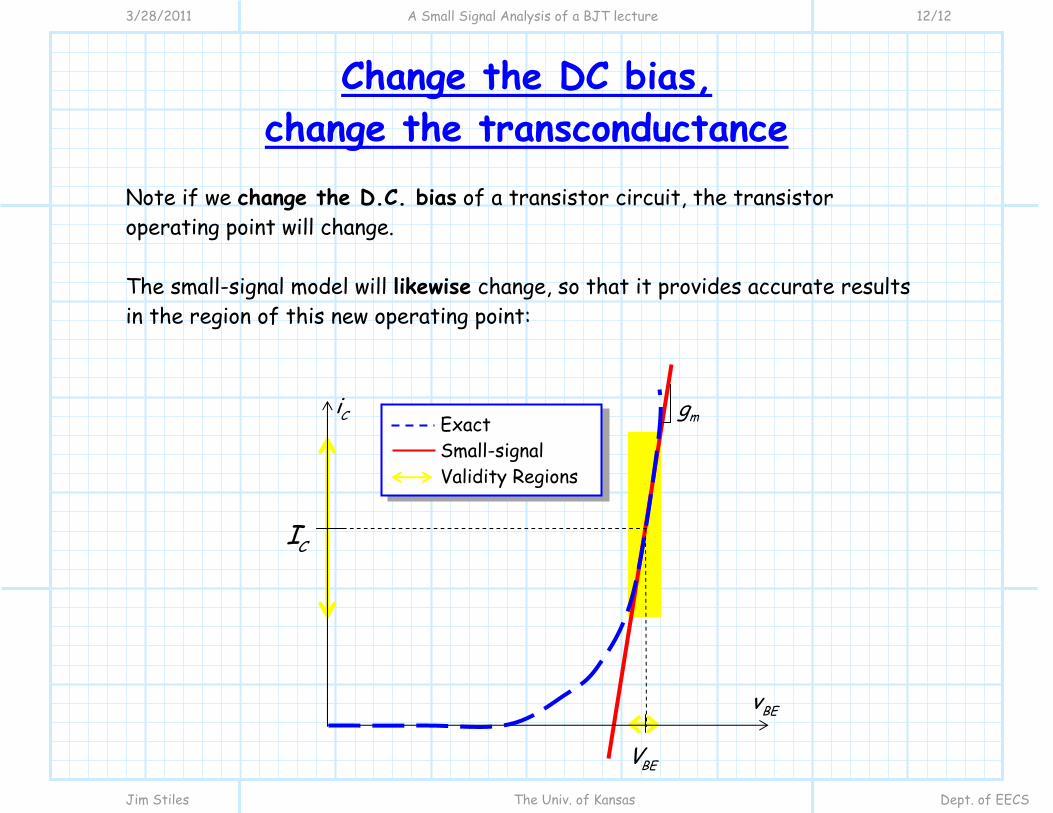
Change the DC bias, change the transconductance
Note if we change the D.C. bias of a transistor circuit, the transistor operating point will change. The small-signal model will likewise change, so that it provides accurate results in the region of this new operating point:
CI
Ci
BEv
BEV
mg Exact Small-signal Validity Regions
3/30/2011 Example A Small Signal BJT Approximation 1/3
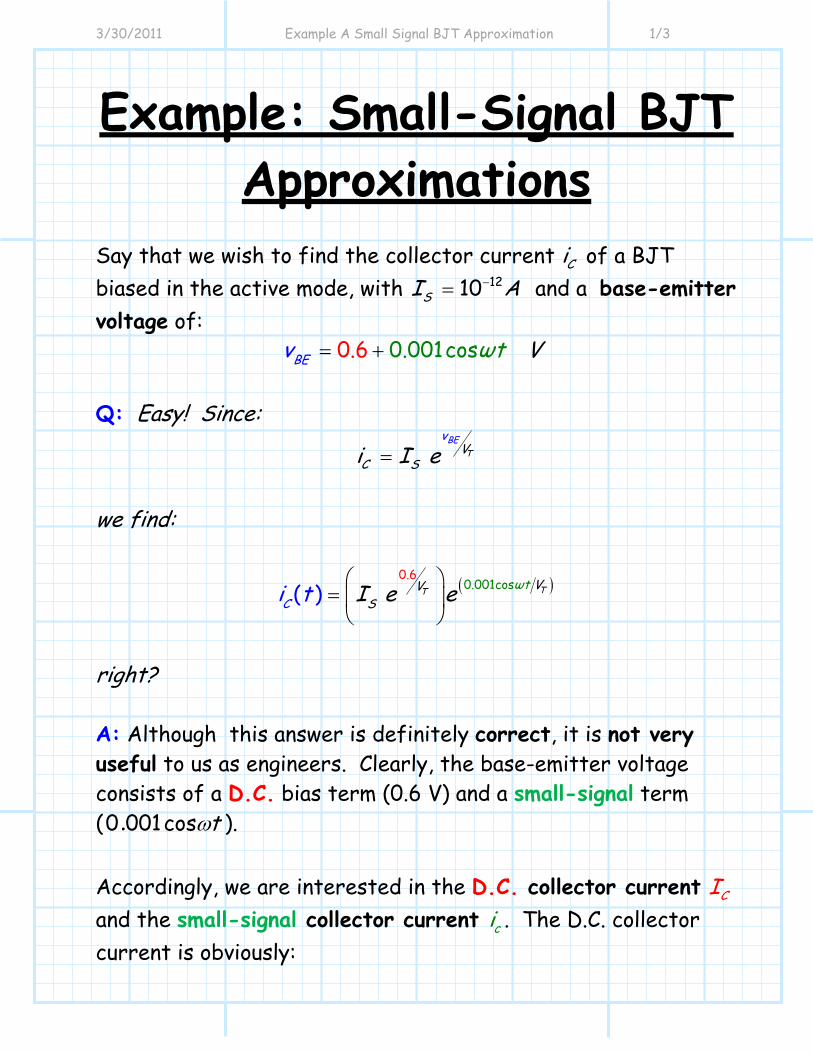
Example: Small-Signal BJT Approximations
Say that we wish to find the collector current Ci of a BJT biased in the active mode, with 1210SI A−= and a base-emitter voltage of:
0.001.6 s0 coBE tv Vω= + Q: Easy! Since:
BETV
C S
v
i I e=
we find:
( )0.0010
co6
s.
( ) TTSC
VV ωtI e ei t ⎛ ⎞= ⎜ ⎟⎝ ⎠
right? A: Although this answer is definitely correct, it is not very useful to us as engineers. Clearly, the base-emitter voltage consists of a D.C. bias term (0.6 V) and a small-signal term (0 001cos. tω ). Accordingly, we are interested in the D.C. collector current CI and the small-signal collector current ci . The D.C. collector current is obviously:
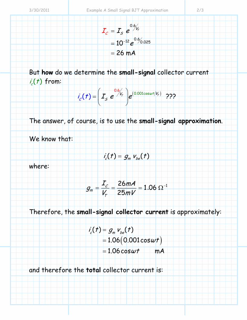
3/30/2011 Example A Small Signal BJT Approximation 2/3
0 6
0 612 0 0251026 mA
TVSCI I e
e−
=
==
.
..
But how do we determine the small-signal collector current
( )ci t from:
( )0.0010
co6
s.
( ) TTSC
VV ωtI e ei t ⎛ ⎞= ⎜ ⎟⎝ ⎠
???
The answer, of course, is to use the small-signal approximation. We know that:
( ) ( )c m bei t g v t= where:
126 1 0625
.Cm
T
I mAgV mV
−= = = Ω
Therefore, the small-signal collector current is approximately:
( )( ) ( )
1.06 0.001cos1.06cos mA
c m bei t g v tωt
ωt
=
=
=
and therefore the total collector current is:
3/30/2011 Example A Small Signal BJT Approximation 3/3
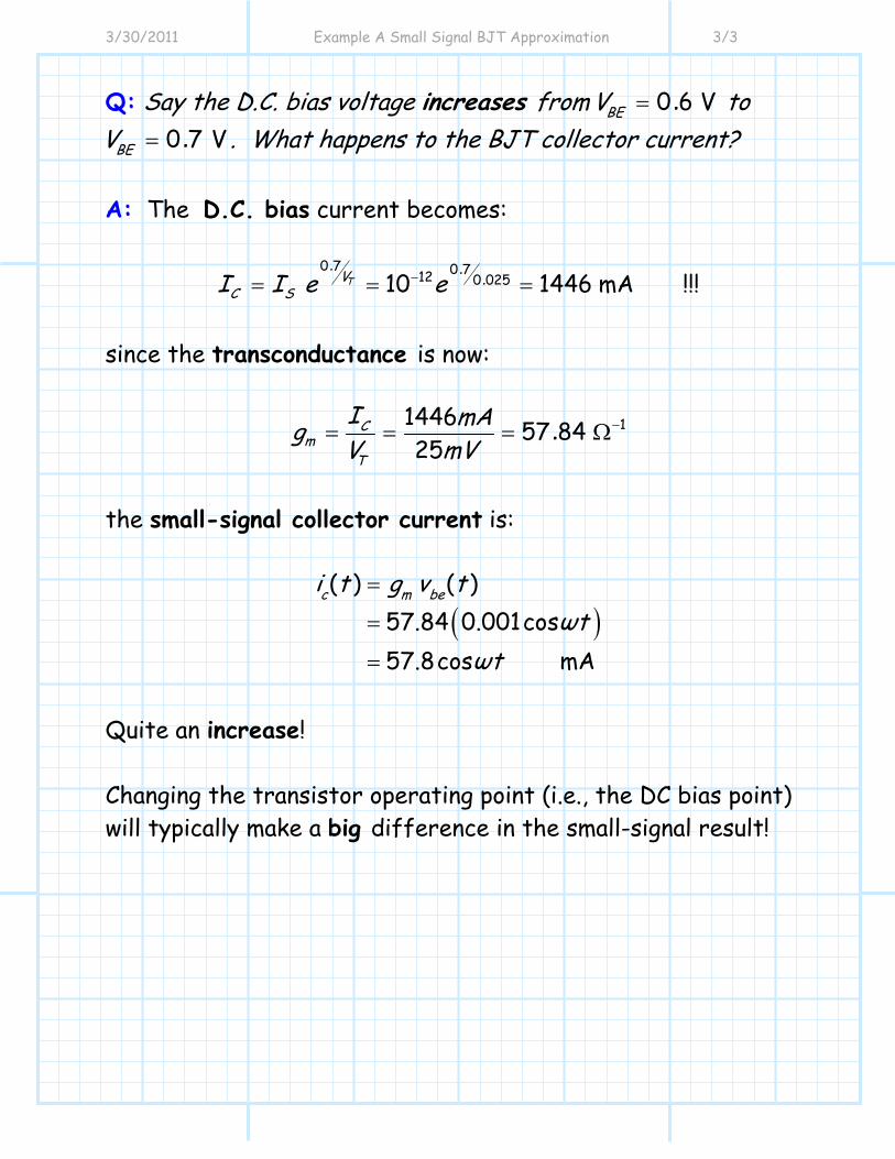
Q: Say the D.C. bias voltage increases from 0 6 V.BEV = to 0 7 V.BEV = . What happens to the BJT collector current?
A: The D.C. bias current becomes:
0 7 0 712 0 02510 1446 mA !!!TVC SI I e e−= = =
. ..
since the transconductance is now:
11446 57 8425
.Cm
T
I mAgV mV
−= = = Ω
the small-signal collector current is:
( )( ) ( )
57.84 0.001cos57.8cos mA
c m bei t g v tωt
ωt
=
=
=
Quite an increase! Changing the transistor operating point (i.e., the DC bias point) will typically make a big difference in the small-signal result!
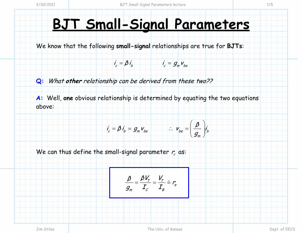
3/30/2011 BJT Small Signal Parameters lecture 1/5
Jim Stiles The Univ. of Kansas Dept. of EECS
BJT Small-Signal Parameters We know that the following small-signal relationships are true for BJTs:
c b c m bei β i i g v= =
Q: What other relationship can be derived from these two?? A: Well, one obvious relationship is determined by equating the two equations above:
c b m be be bm
βi β i g v v ig
⎛ ⎞= = ∴ = ⎜ ⎟⎜ ⎟
⎝ ⎠
We can thus define the small-signal parameter rπ as:
T Tπ
m C B
βV Vβ rg I I
= =
3/30/2011 BJT Small Signal Parameters lecture 2/5
Jim Stiles The Univ. of Kansas Dept. of EECS
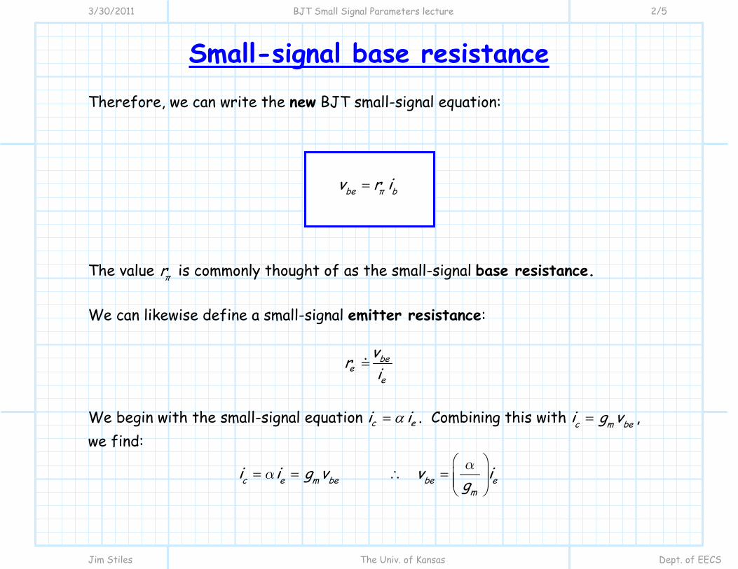
Small-signal base resistance Therefore, we can write the new BJT small-signal equation:
be π bv r i=
The value πr is commonly thought of as the small-signal base resistance. We can likewise define a small-signal emitter resistance:
bee
e
vri
We begin with the small-signal equation c ei iα= . Combining this with c m bei g v= , we find:
c e m be be em
i i g v v ig
⎛ ⎞= = ∴ = ⎜ ⎟⎜ ⎟
⎝ ⎠
αα

3/30/2011 BJT Small Signal Parameters lecture 3/5
Jim Stiles The Univ. of Kansas Dept. of EECS
Small-signal emitter resistance We can thus define the small-signal parameter er as:
T Te
m C E
V V rg I I
αα= =
Therefore, we can write another new BJT small-signal equation:
e ebev r i=
Note that in addition to β , we now have three fundamental BJT small-signal parameters:
C T Tm e
BT E
I V Vg r rV I Iπ= = =
3/30/2011 BJT Small Signal Parameters lecture 4/5
Jim Stiles The Univ. of Kansas Dept. of EECS
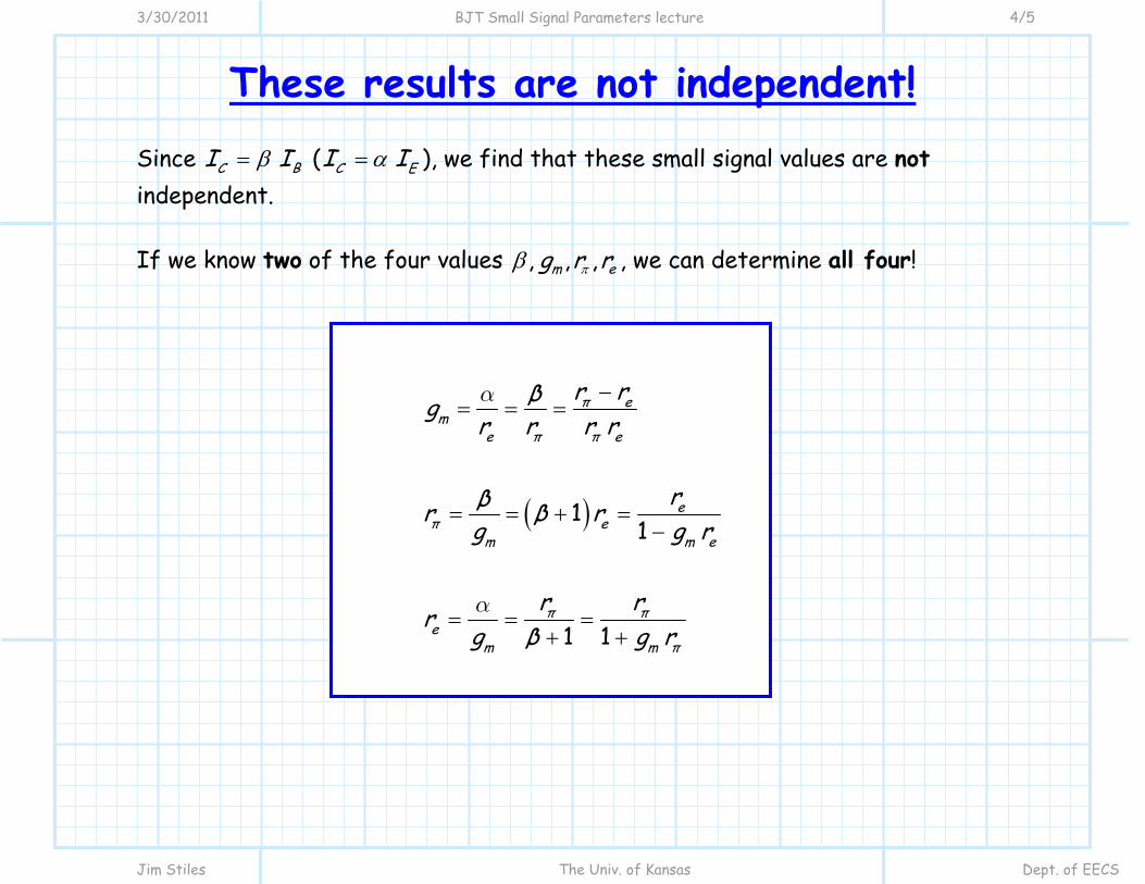
These results are not independent! Since BCI Iβ= ( C EI Iα= ), we find that these small signal values are not independent. If we know two of the four values , , ,m eg r rπβ , we can determine all four!
( )1 1
1 1
π em
e π π e
eπ e
m m e
π πe
m m π
r rβgr r r r
rβr β rg g r
r rrg β g r
−= = =
= = + =−
= = =+ +
α
α
3/30/2011 BJT Small Signal Parameters lecture 5/5
Jim Stiles The Univ. of Kansas Dept. of EECS
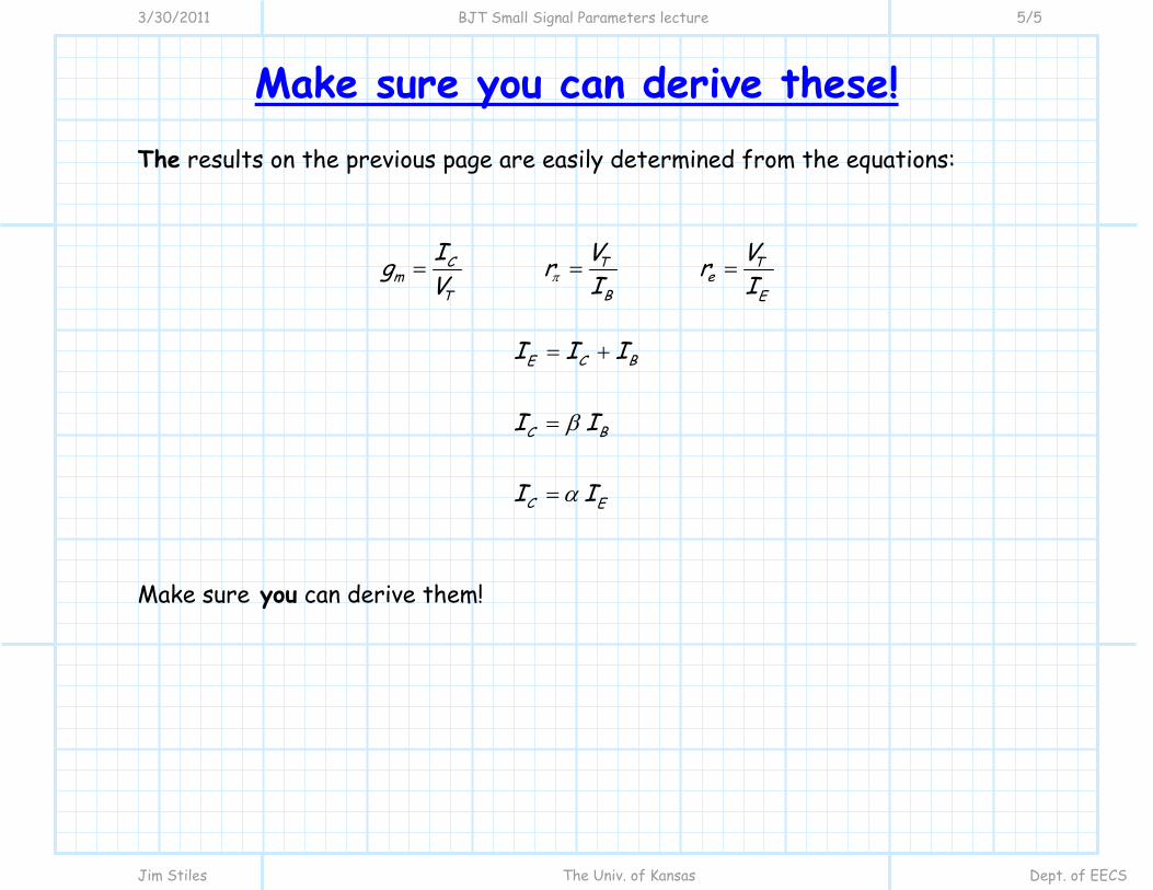
Make sure you can derive these! The results on the previous page are easily determined from the equations:
C T Tm e
BT E
I V Vg r rV I Iπ= = =
BCE
BC
C E
I I I
I I
I I
β
α
= +
=
=
Make sure you can derive them!
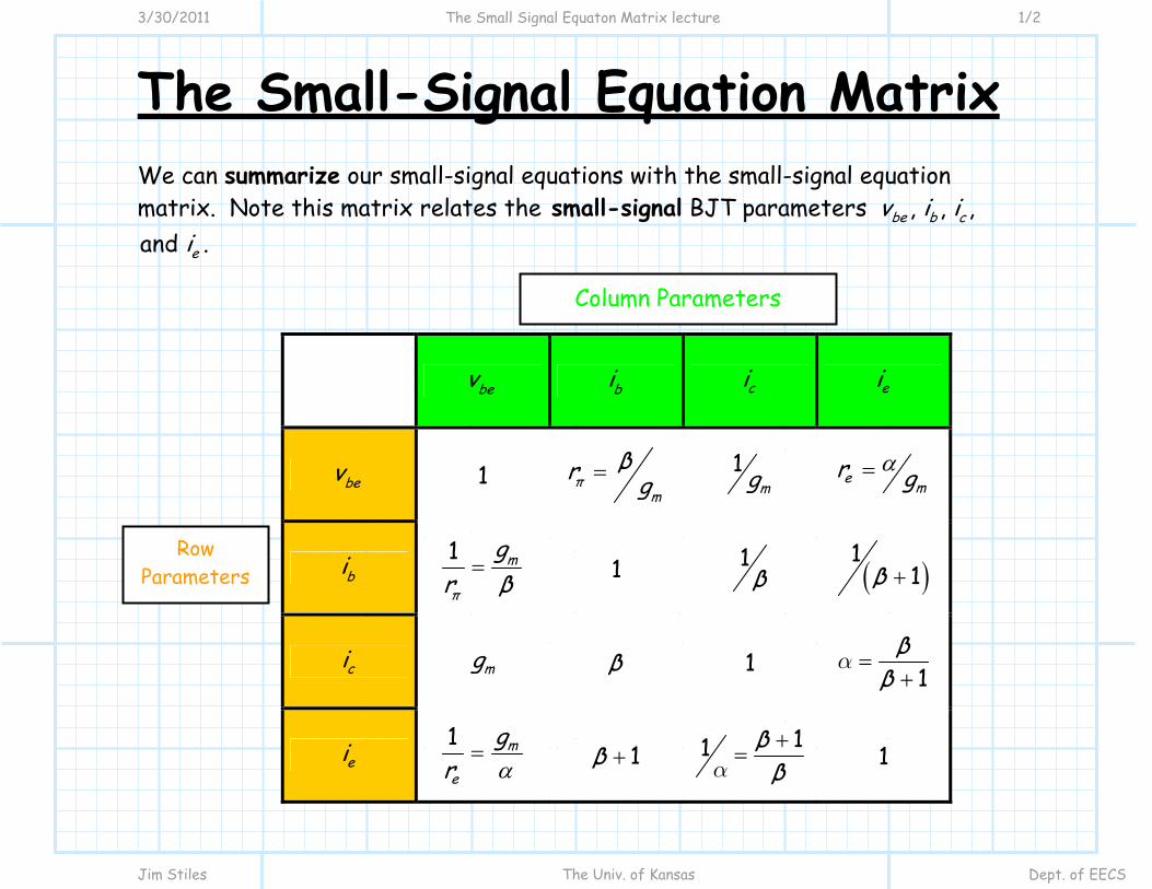
3/30/2011 The Small Signal Equaton Matrix lecture 1/2
Jim Stiles The Univ. of Kansas Dept. of EECS
The Small-Signal Equation Matrix We can summarize our small-signal equations with the small-signal equation matrix. Note this matrix relates the small-signal BJT parameters , , , be b cv i i and ei .
bev bi ci ei
bev 1 πm
βr g= 1mg e m
r gα=
bi 1 m
π
gr β
= 1 1β ( )
11β +
ci mg β 1 1β
β=
+α
ei 1 m
e
gr α
= 1β + 11 β
β+
=α
1
Column Parameters
Row Parameters

3/30/2011 The Small Signal Equaton Matrix lecture 2/2
Jim Stiles The Univ. of Kansas Dept. of EECS
Here’s how you use this To use this matrix, note that the row parameter is equal to the product of the column parameter and the matrix element. For example:
1bb er
i vπ
=
bev bi ci ei
bev 1 πm
βr g= 1mg e m
r gα=
bi 1 m
π
gr β
= 1 1β ( )
11β +
ci mg β 1 1β
β=
+α
ei 1 m
e
gr α
= 1β + 11 β
β+
=α
1
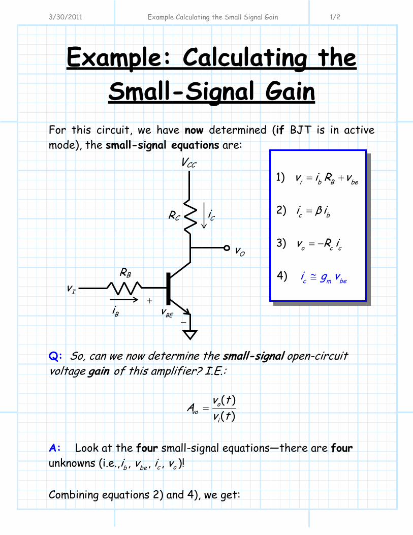
3/30/2011 Example Calculating the Small Signal Gain 1/2
Example: Calculating the Small-Signal Gain
For this circuit, we have now determined (if BJT is in active mode), the small-signal equations are: Q: So, can we now determine the small-signal open-circuit voltage gain of this amplifier? I.E.:
( )( )
ovo
i
v tAv t
=
A: Look at the four small-signal equations—there are four unknowns (i.e., , , , c ob bei v i v )! Combining equations 2) and 4), we get:
1)
2)
3)
4)
i b B be
c b
c m b
c
e
o c
v i R v
i β i
v R i
i g v≅
= +
=
= −
RC
Iv RB
VCC
Ci
Bi
Ov
BEv+
−

3/30/2011 Example Calculating the Small Signal Gain 2/2
be b π bm
βv i r ig
= =
Inserting this result in equation 1), we find:
( )i B π bv R r i= +
Therefore: i
bB π
viR r
=+
and since c bi β i= :
c iB π
βi vR r
=+
which we insert into equation 3):
C
o c C iB π
βRv i R vR r−
= − =+
Therefore, the small-signal gain of this amplifier is:
( )( )
o Cvo
i B π
v t β RAv t R r
−= =
+
Note this is the small signal gain of this amplifier—and this amplifier only!
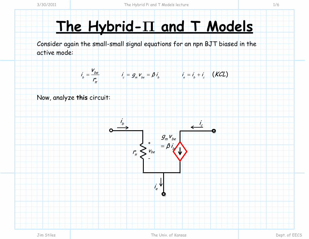
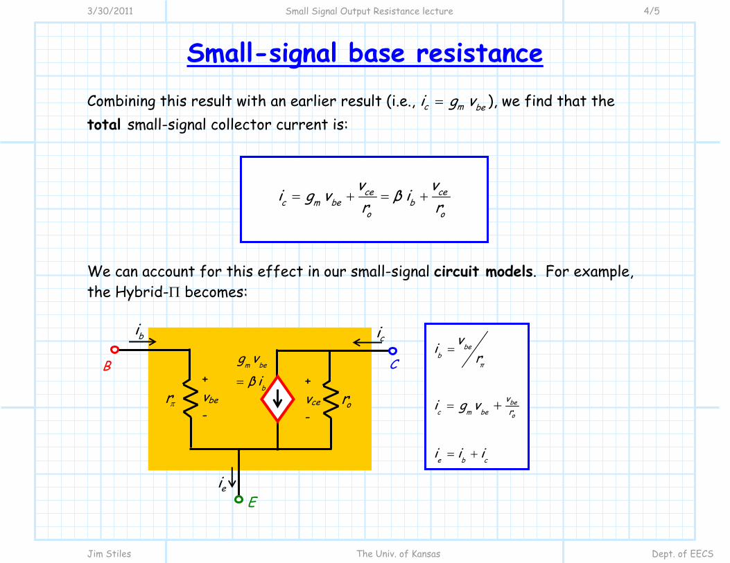
3/30/2011 The Hybrid Pi and T Models lecture 1/6
Jim Stiles The Univ. of Kansas Dept. of EECS
The Hybrid-Π and T Models Consider again the small-small signal equations for an npn BJT biased in the active mode:
( )b c m be b e b cbe
π
i i g v β i i i iv KCLr
= = = = +
Now, analyze this circuit:
+ vbe -
πr
m be
b
g vβ i=
bi ci
ei
3/30/2011 The Hybrid Pi and T Models lecture 2/6
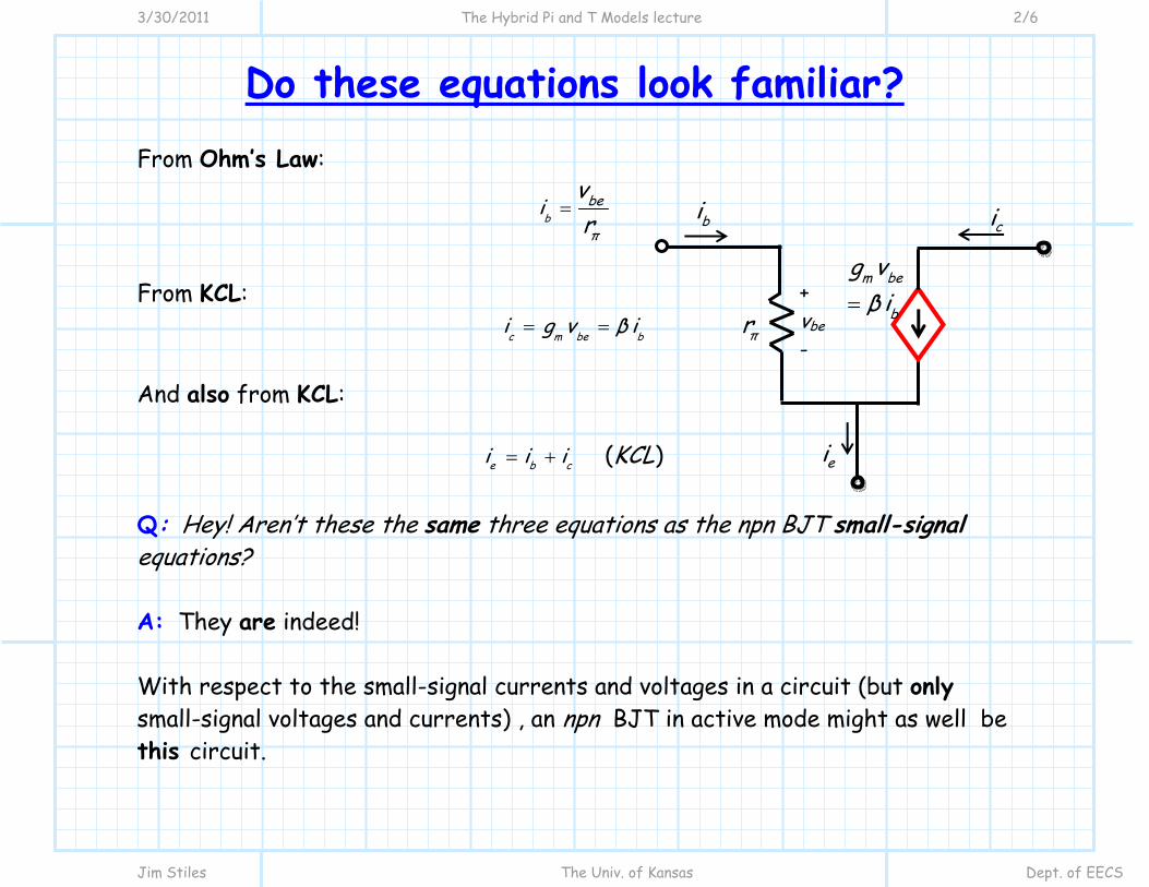
Jim Stiles The Univ. of Kansas Dept. of EECS
Do these equations look familiar? From Ohm’s Law:
bbe
π
ivr
=
From KCL:
c m be bi g v β i= =
And also from KCL:
( )e b ci i i KCL= + Q: Hey! Aren’t these the same three equations as the npn BJT small-signal equations? A: They are indeed! With respect to the small-signal currents and voltages in a circuit (but only small-signal voltages and currents) , an npn BJT in active mode might as well be this circuit.
+ vbe -
πr
m be
b
g vβ i=
bi ci
ei
3/30/2011 The Hybrid Pi and T Models lecture 3/6
Jim Stiles The Univ. of Kansas Dept. of EECS
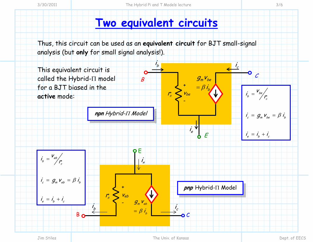
Two equivalent circuits Thus, this circuit can be used as an equivalent circuit for BJT small-signal analysis (but only for small signal analysis!). This equivalent circuit is called the Hybrid-Π model for a BJT biased in the active mode:
ebb
c m eb b
e b c
vi r
i g v i
i i i
π
β
=
= =
= +
+ veb -
rπ m eb
b
g viβ=
bi ci
ei
B C
E
E
beb
c m be b
e b c
vi r
i g v i
i i i
π
β
=
= =
= +
npn Hybrid-Π Model
+ vbe -
rπ
m be
b
g vi= β
bi ci
ei
B C
pnp Hybrid-Π Model

3/30/2011 The Hybrid Pi and T Models lecture 4/6
Jim Stiles The Univ. of Kansas Dept. of EECS
An alternative equivalent circuit Note however, that we can alternatively express the small-signal circuit equations as:
beb e c c m be b e
e
vi i i i g v β i ir
= = = =−
These equations likewise describes the T-Model—an alternative but equivalent model to the Hybrid-Π.
b e c
c m be b
ebe
e
i i i
i g v β i
ivr
=
= =
=
−
npn T-Model
+ vbe -
er
m be
b
g vβ i=
bi
ci
ei
B
C
E
3/30/2011 The Hybrid Pi and T Models lecture 5/6
Jim Stiles The Univ. of Kansas Dept. of EECS
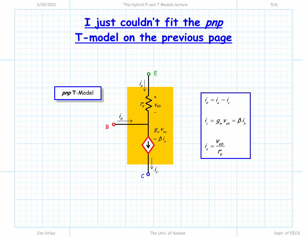
I just couldn’t fit the pnp T-model on the previous page
pnp T-Model + veb -
er
m be
b
g vβ i=
bi
ci
ei
B
C
E
b e c
c m eb b
eeb
e
i i i
i g v β i
ivr
=
= =
=
−
3/30/2011 The Hybrid Pi and T Models lecture 6/6
Jim Stiles The Univ. of Kansas Dept. of EECS
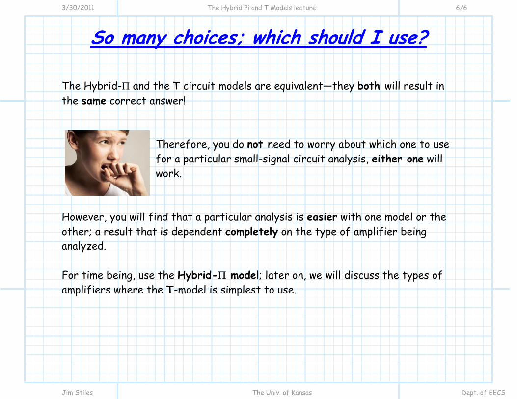
So many choices; which should I use? The Hybrid-Π and the T circuit models are equivalent—they both will result in the same correct answer!
Therefore, you do not need to worry about which one to use for a particular small-signal circuit analysis, either one will work.
However, you will find that a particular analysis is easier with one model or the other; a result that is dependent completely on the type of amplifier being analyzed. For time being, use the Hybrid-Π model; later on, we will discuss the types of amplifiers where the T-model is simplest to use.

3/30/2011 Small Signal Output Resistance lecture 1/5
Jim Stiles The Univ. of Kansas Dept. of EECS
Small-Signal Output Resistance Recall that due to the Early effect, the collector current Ci is slightly dependent on CEv :
1 CEC B
A
vi β iV
⎛ ⎞= +⎜ ⎟
⎝ ⎠
where we recall that AV is a BJT device parameter, called the Early Voltage. Q: How does this affect the small-signal response of the BJT? A: Well, if ( ) ( )C C ci I it t= + and ( ) ( )CE CE cev V vt t= + , then with the small-signal approximation:
1
11 1
CE CECE CE
CCEC c B ce
CE v VA v V
CE CEB B ce
AA A
ivI i β i vvV
V Vβ I β I vVV V
==
⎛ ⎞∂⎛ ⎞⎜ ⎟+ = + +⎜ ⎟ ∂⎜ ⎟⎝ ⎠ ⎝ ⎠
⎛ ⎞ ⎛ ⎞ ⎛ ⎞= + + +⎜ ⎟ ⎜ ⎟ ⎜ ⎟
⎝ ⎠⎝ ⎠ ⎝ ⎠
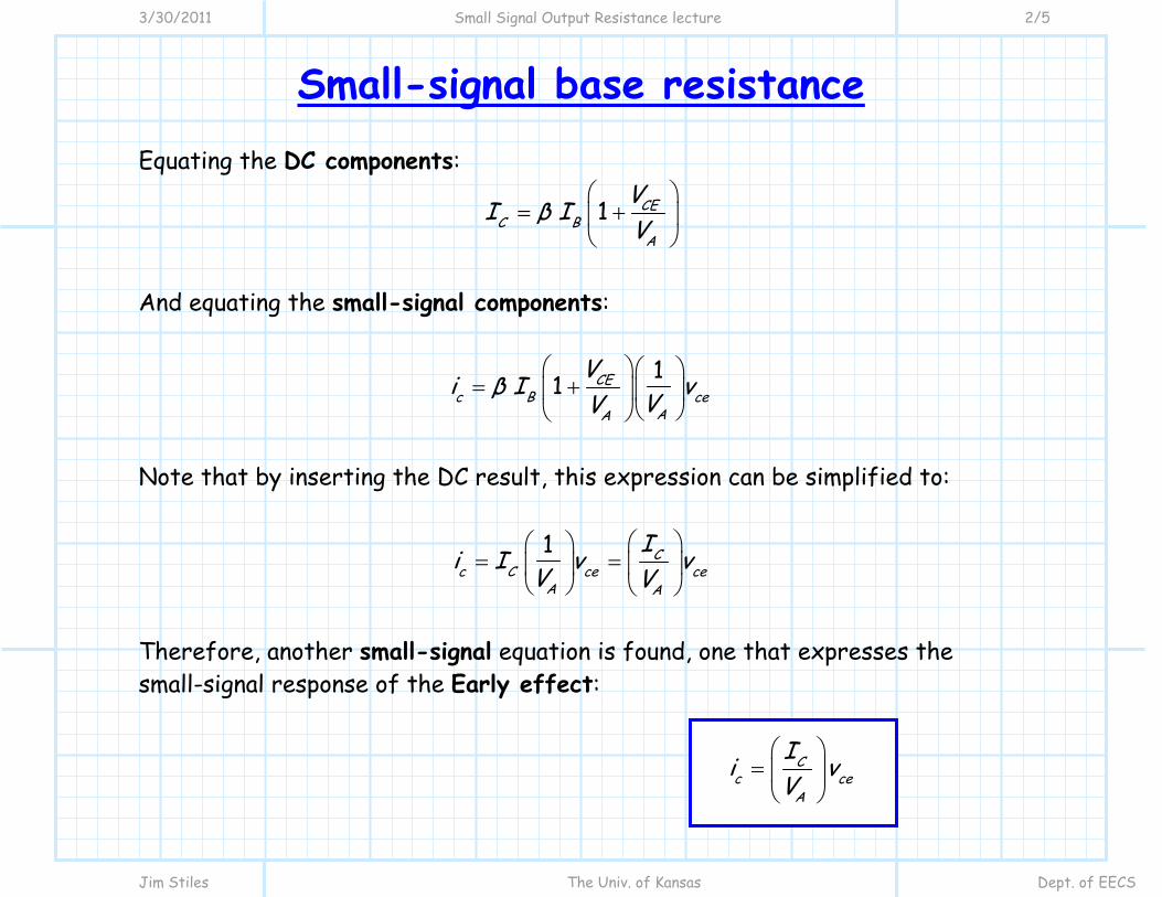
3/30/2011 Small Signal Output Resistance lecture 2/5
Jim Stiles The Univ. of Kansas Dept. of EECS
Small-signal base resistance Equating the DC components:
1 CEC B
A
VI β IV
⎛ ⎞= +⎜ ⎟
⎝ ⎠
And equating the small-signal components:
11 CEc B ce
AA
Vi β I vVV⎛ ⎞ ⎛ ⎞
= +⎜ ⎟ ⎜ ⎟⎝ ⎠⎝ ⎠
Note that by inserting the DC result, this expression can be simplified to:
1 Cc C ce ce
A A
Ii I v vV V⎛ ⎞⎛ ⎞
= = ⎜ ⎟⎜ ⎟⎝ ⎠ ⎝ ⎠
Therefore, another small-signal equation is found, one that expresses the small-signal response of the Early effect:
Cc ce
A
Ii vV⎛ ⎞
= ⎜ ⎟⎝ ⎠
3/30/2011 Small Signal Output Resistance lecture 3/5
Jim Stiles The Univ. of Kansas Dept. of EECS
Small-signal base resistance Recall that we defined (in EECS 312) the BJT output resistance or :
1C
oA
IV r
Be careful! Although the Early Voltage AV is a device parameter, the output resistance or —since it depends on DC collector current CI —is not a device parameter!
Therefore, the small-signal collector current resulting from the Early effect can likewise be expressed as:
cec
o
vir
=
3/30/2011 Small Signal Output Resistance lecture 4/5
Jim Stiles The Univ. of Kansas Dept. of EECS
Small-signal base resistance Combining this result with an earlier result (i.e., c m bei g v= ), we find that the total small-signal collector current is:
ce ce
c m be bo o
v vi g v β ir r
= + = +
We can account for this effect in our small-signal circuit models. For example, the Hybrid-Π becomes:
be
o
beb
π
c m be
e b c
vr
vi r
i g v
i i i
=
=
= +
+
E
+ vbe -
rπ
m be
b
g vβ i=
bi ci
ei
B C + vce -
or

3/30/2011 Small Signal Output Resistance lecture 5/5
Jim Stiles The Univ. of Kansas Dept. of EECS
Small-signal base resistance And for the T-model:
Often, or is so large that it can be ignored (caution: ignoring the output resistance means approximating it as an open circuit, i.e., or = ∞ ).
+ vbe -
er
m be
b
g vβ i=
bi
ci
ei
B
C
E
+ vce -
or

4/1/2011 Steps for Small Signal Analysis lecture 1/14
Jim Stiles The Univ. of Kansas Dept. of EECS
BJT Small-Signal Analysis Steps
Complete each of these steps if you choose to correctly complete a BJT Amplifier small-signal analysis. Step 1: Complete a D.C. Analysis Turn off all small-signal sources, and then complete a circuit analysis with the remaining D.C. sources only.
* Complete this DC analysis exactly, precisely, the same way you performed the DC analysis in section 5.4. That is, you assume (the active mode), enforce, analyze, and check (do not forget to check!). * Note that you enforce and check exactly, precisely the same the same equalities and inequalities as discussed in section 5.4 (e.g., 0 7 V.BEV = ,
0CBV > ).
4/1/2011 Steps for Small Signal Analysis lecture 2/14
Jim Stiles The Univ. of Kansas Dept. of EECS
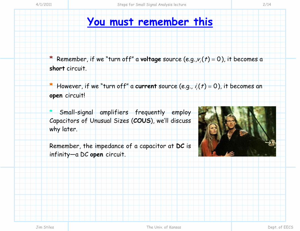
You must remember this * Remember, if we “turn off” a voltage source (e.g., ( ) 0iv t = ), it becomes a short circuit. * However, if we “turn off” a current source (e.g., ( ) 0ii t = ), it becomes an open circuit!
* Small-signal amplifiers frequently employ
Capacitors of Unusual Sizes (COUS), we’ll discuss why later.
Remember, the impedance of a capacitor at DC is infinity—a DC open circuit.

4/1/2011 Steps for Small Signal Analysis lecture 3/14
Jim Stiles The Univ. of Kansas Dept. of EECS
The goals of DC analysis— and don’t forget to CHECK
The goal of this DC analysis is to determine:
1) One of the DC BJT currents ( , , B C EI I I ) for each BJT. 2) Either the voltage or CB CEV V for each BJT.
You do not necessarily need to determine any other DC currents or voltages within the amplifier circuit!
Once you have found these values, you can CHECK your active assumption, and then move on to step 2.
4/1/2011 Steps for Small Signal Analysis lecture 4/14
Jim Stiles The Univ. of Kansas Dept. of EECS
The DC bias terms are required to determine our small-signal parameters
A: Remember, all of the small-signal BJT parameters (e.g., , , , m e og r r rπ ) are dependent on D.C. values (e.g., , , BC EI I I ). In other words, we must first determine the operating (i.e., bias) point of the transistor in order to determine its small-signal performance!
Q: I’m perplexed. I was eagerly anticipating the steps for small-signal analysis, yet you’re saying we should complete a DC analysis. Why are we doing this—why do we care what any of the DC voltages and currents are?
4/1/2011 Steps for Small Signal Analysis lecture 5/14
Jim Stiles The Univ. of Kansas Dept. of EECS
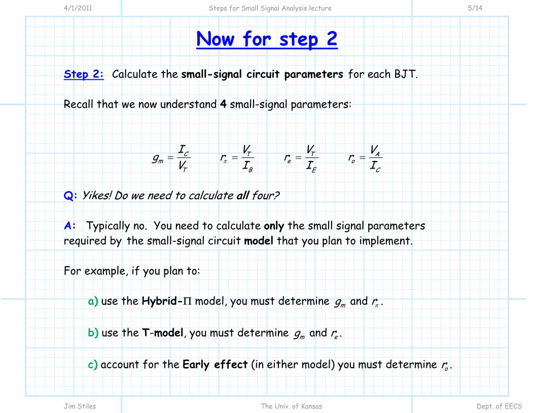
Now for step 2 Step 2: Calculate the small-signal circuit parameters for each BJT. Recall that we now understand 4 small-signal parameters:
C T T Am e o
BT CE
I V V Vg r r rV I I Iπ= = = =
Q: Yikes! Do we need to calculate all four? A: Typically no. You need to calculate only the small signal parameters required by the small-signal circuit model that you plan to implement.
For example, if you plan to:
a) use the Hybrid-Π model, you must determine and mg rπ .
b) use the T-model, you must determine and m eg r .
c) account for the Early effect (in either model) you must determine or .
4/1/2011 Steps for Small Signal Analysis lecture 6/14
Jim Stiles The Univ. of Kansas Dept. of EECS
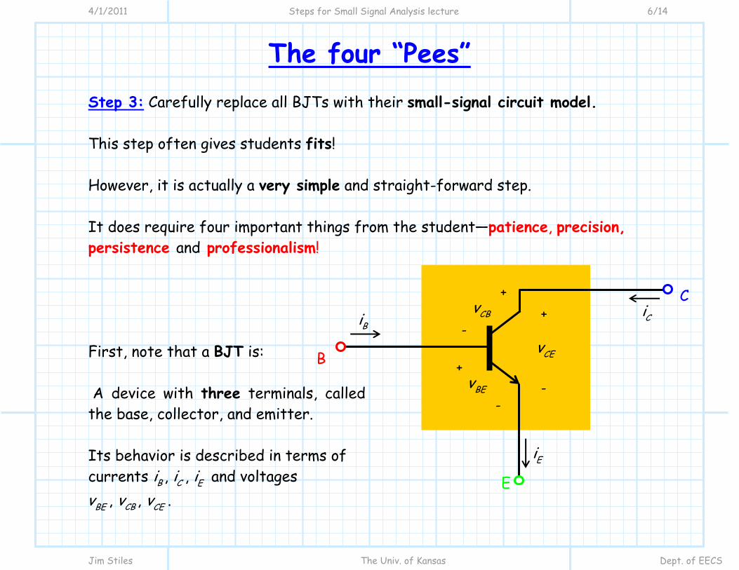
The four “Pees” Step 3: Carefully replace all BJTs with their small-signal circuit model. This step often gives students fits! However, it is actually a very simple and straight-forward step. It does require four important things from the student—patience, precision, persistence and professionalism! First, note that a BJT is: A device with three terminals, called the base, collector, and emitter. Its behavior is described in terms of currents , , B C Ei i i and voltages
, , CBBE CEv v v .
Ci
Ei
Bi
+ BEv -
+
CEv -
+ CBv -
B
E
C
4/1/2011 Steps for Small Signal Analysis lecture 7/14
Jim Stiles The Univ. of Kansas Dept. of EECS
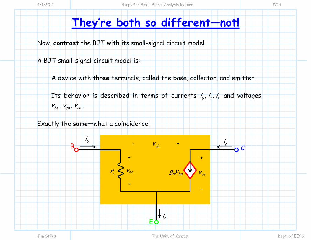
They’re both so different—not! Now, contrast the BJT with its small-signal circuit model. A BJT small-signal circuit model is:
A device with three terminals, called the base, collector, and emitter. Its behavior is described in terms of currents , , c ebi i i and voltages
, , cebe cbv v v . Exactly the same—what a coincidence!
+
cev -
- cbv + B
E
C +
vbe -
rπ m beg v
bi ci
ei
4/1/2011 Steps for Small Signal Analysis lecture 8/14
Jim Stiles The Univ. of Kansas Dept. of EECS
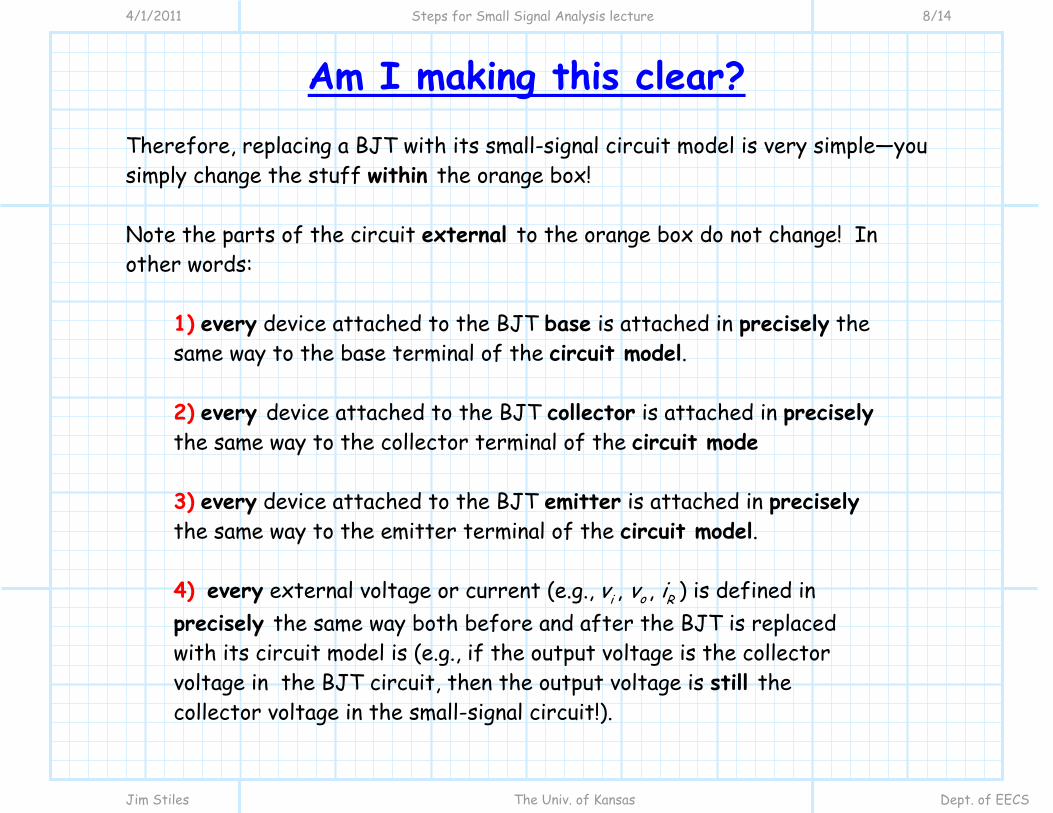
Am I making this clear? Therefore, replacing a BJT with its small-signal circuit model is very simple—you simply change the stuff within the orange box! Note the parts of the circuit external to the orange box do not change! In other words:
1) every device attached to the BJT base is attached in precisely the same way to the base terminal of the circuit model. 2) every device attached to the BJT collector is attached in precisely the same way to the collector terminal of the circuit mode 3) every device attached to the BJT emitter is attached in precisely the same way to the emitter terminal of the circuit model.
4) every external voltage or current (e.g., , , oi Rv v i ) is defined in precisely the same way both before and after the BJT is replaced with its circuit model is (e.g., if the output voltage is the collector voltage in the BJT circuit, then the output voltage is still the collector voltage in the small-signal circuit!).
4/1/2011 Steps for Small Signal Analysis lecture 9/14
Jim Stiles The Univ. of Kansas Dept. of EECS
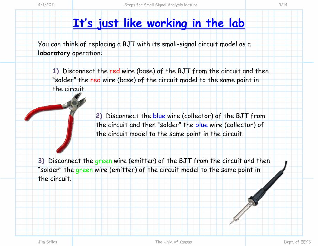
It’s just like working in the lab You can think of replacing a BJT with its small-signal circuit model as a laboratory operation:
1) Disconnect the red wire (base) of the BJT from the circuit and then “solder” the red wire (base) of the circuit model to the same point in the circuit.
2) Disconnect the blue wire (collector) of the BJT from the circuit and then “solder” the blue wire (collector) of the circuit model to the same point in the circuit.
3) Disconnect the green wire (emitter) of the BJT from the circuit and then “solder” the green wire (emitter) of the circuit model to the same point in the circuit.
4/1/2011 Steps for Small Signal Analysis lecture 10/14
Jim Stiles The Univ. of Kansas Dept. of EECS
This is superposition— turn off the DC sources!
Step 4: Set all D.C. sources to zero. Remember: A zero-voltage DC source is a short circuit. A zero-current DC source is an open circuit. The schematic in now in front of you is called the small-signal circuit. Note that it is missing two things—DC sources and bipolar junction transistors!
* Note that steps three and four are reversible. You could turn off the DC sources first, and then replace all BJTs with their small-signal models—the resulting small-signal circuit will be the same! * You will find that the small-signal circuit schematic can often be greatly simplified.
4/1/2011 Steps for Small Signal Analysis lecture 11/14
Jim Stiles The Univ. of Kansas Dept. of EECS
Many things will be connected to ground! Once the DC voltage sources are turned off, you will find that the terminals of many devices are connected to ground.
* Remember, all terminals connected to ground are also connected to each other! For example, if the emitter terminal is connected to ground, and one terminal of a resistor is connected to ground, then that resistor terminal is connected to the emitter! * As a result, you often find that resistors in different parts of the circuit are actually connected in parallel, and thus can be combined to simplify the circuit schematic! * Finally, note that the AC impedance of a COUS (i.e., 1CZ Cω= ) is small for all but the lowest frequencies ω . If this impedance is smaller than the other circuit elements (e.g., < 10Ω), we can view the impedance as approximately zero, and thus replace the large capacitor with a (AC) short!
4/1/2011 Steps for Small Signal Analysis lecture 12/14
Jim Stiles The Univ. of Kansas Dept. of EECS
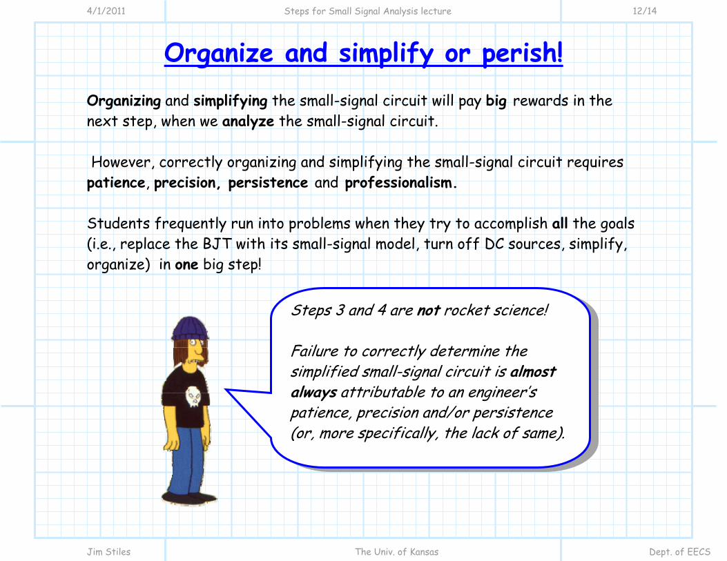
Organize and simplify or perish! Organizing and simplifying the small-signal circuit will pay big rewards in the next step, when we analyze the small-signal circuit. However, correctly organizing and simplifying the small-signal circuit requires patience, precision, persistence and professionalism. Students frequently run into problems when they try to accomplish all the goals (i.e., replace the BJT with its small-signal model, turn off DC sources, simplify, organize) in one big step!
Steps 3 and 4 are not rocket science! Failure to correctly determine the simplified small-signal circuit is almost always attributable to an engineer’s patience, precision and/or persistence (or, more specifically, the lack of same).
4/1/2011 Steps for Small Signal Analysis lecture 13/14
Jim Stiles The Univ. of Kansas Dept. of EECS
This is a EECS 211 problem, and only a 211 problem
Step 5: Analyze small-signal circuit. We now can analyze the small-signal circuit to find all small-signal voltages and currents.
* For small-signal amplifiers, we typically attempt to find the small-signal output voltage ov in terms of the small-signal input voltage iv . From this result, we can find the voltage gain of the amplifier. * Note that this analysis requires only the knowledge you acquired in EECS 211! The small-signal circuit will consist entirely of resistors and (small-signal) voltage/current sources. These are precisely the same resistors and sources that you learned about in EECS 211. You analyze them in precisely the same way.
4/1/2011 Steps for Small Signal Analysis lecture 14/14
Jim Stiles The Univ. of Kansas Dept. of EECS
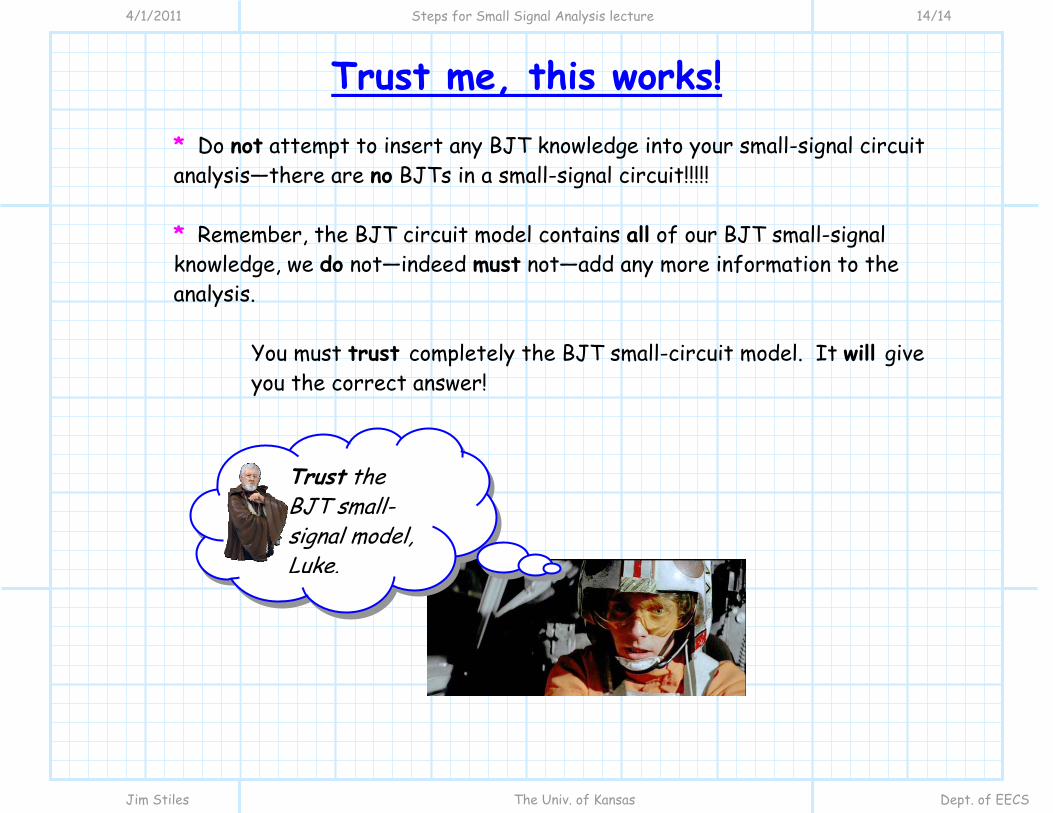
Trust me, this works!
* Do not attempt to insert any BJT knowledge into your small-signal circuit analysis—there are no BJTs in a small-signal circuit!!!!! * Remember, the BJT circuit model contains all of our BJT small-signal knowledge, we do not—indeed must not—add any more information to the analysis.
You must trust completely the BJT small-circuit model. It will give you the correct answer!
Trust the
BJT small-signal model, Luke.
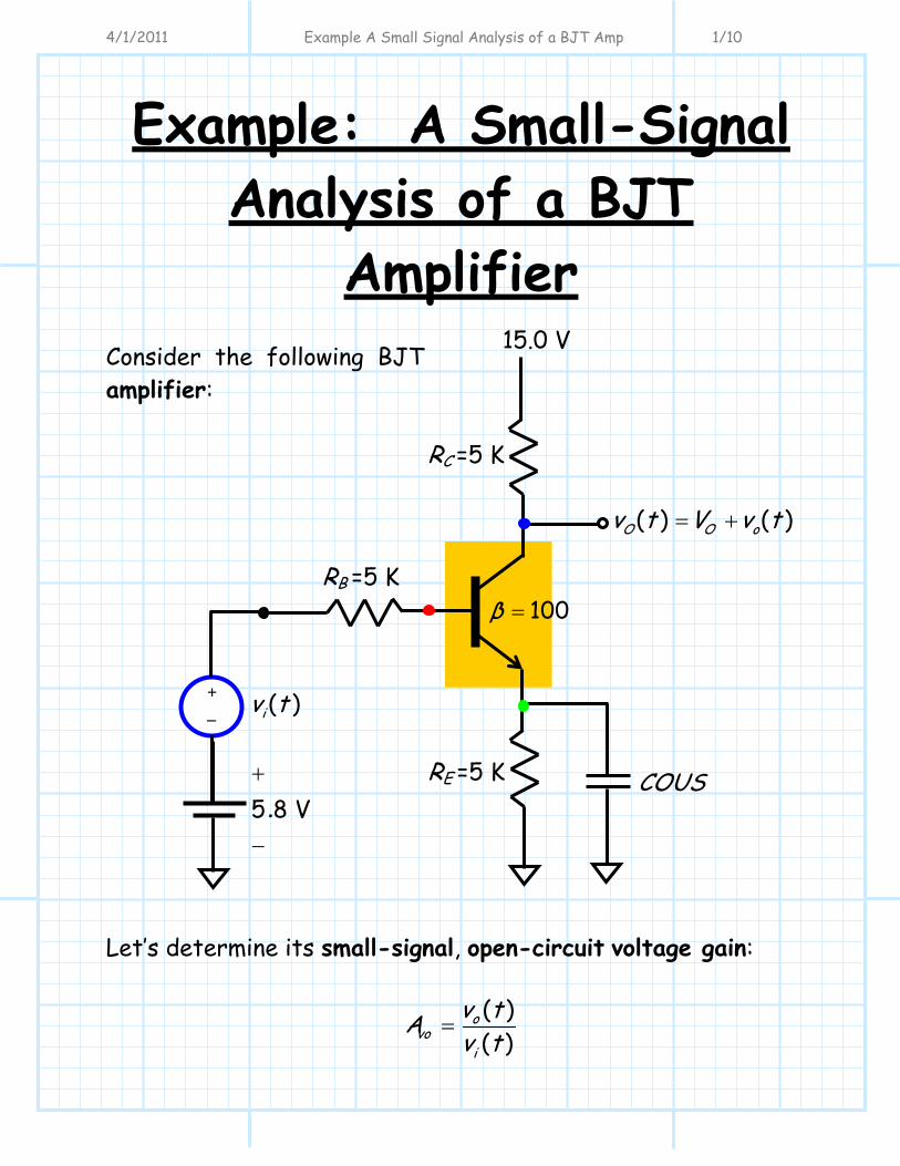
4/1/2011 Example A Small Signal Analysis of a BJT Amp 1/10
Example: A Small-Signal Analysis of a BJT
Amplifier Consider the following BJT amplifier: Let’s determine its small-signal, open-circuit voltage gain:
( )( )
ovo
i
v tAv t
=
( ) ( )O O ov t V v t= +
+ _
15.0 V
( )iv t
5 8 V.+
−
RB =5 K
RC =5 K
RE =5 K COUS
100β =
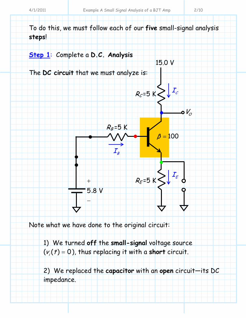
4/1/2011 Example A Small Signal Analysis of a BJT Amp 2/10
To do this, we must follow each of our five small-signal analysis steps! Step 1: Complete a D.C. Analysis The DC circuit that we must analyze is: Note what we have done to the original circuit: 1) We turned off the small-signal voltage source
( ( ) 0iv t = ), thus replacing it with a short circuit. 2) We replaced the capacitor with an open circuit—its DC
impedance.
CI
EI
BI
OV
15.0 V
5 8 V.+
−
RB =5 K
RC =5 K
RE =5 K
100β =

4/1/2011 Example A Small Signal Analysis of a BJT Amp 3/10
Now we proceed with the DC analysis. We ASSUME that the BJT is in active mode, and thus ENFORCE the equalities
0 7 V.BEV = and BCI Iβ= . We now begin to ANALYZE the circuit by writing the Base-Emitter Leg KVL: 5.8 5 0.7 5( 1) 0B BI β I− − − + = Therefore:
5.1 0.01 mA5 5(101)BI = =+
and thus:
1.0 mAC BI βI= =
1.01 mAE B CI I I= + =
Q: Since we know the DC bias currents, we have all the information we need to determine the small-signal parameters. Why don’t we proceed directly to step 2?
CI
EI
BI
OV
15.0 V
5 8 V.+
−
RB =5 K
RC =5 K
RE =5 K
100β =
4/1/2011 Example A Small Signal Analysis of a BJT Amp 4/10
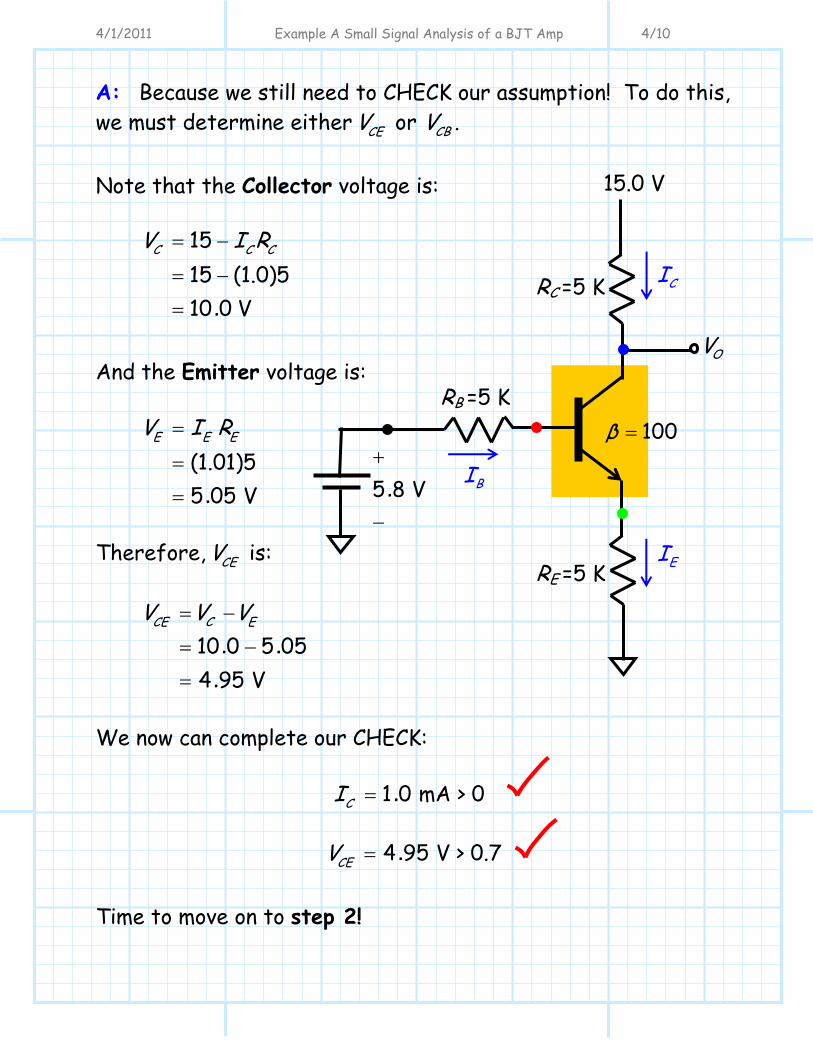
A: Because we still need to CHECK our assumption! To do this, we must determine either or CBCEV V .
Note that the Collector voltage is:
1515 (1.0)510 0 V.
C C CV I R= −
= −
=
And the Emitter voltage is:
(1.01)55 05 V.
E E EV I R=
=
=
Therefore, CEV is:
10 0 5 054 95 V. ..
CCE EV V V= −
= −
=
We now can complete our CHECK:
1 0 mA > 0 .CI =
4 95 V > 0.7.CEV = Time to move on to step 2!
CI
EI
BI
OV
15.0 V
5 8 V.+
−
RB =5 K
RC =5 K
RE =5 K
100β =

4/1/2011 Example A Small Signal Analysis of a BJT Amp 5/10
Step 2: Calculate the small-signal circuit parameters for each BJT. If we use the Hybrid-Π model, we need to determine and mg rπ :
1 040
0 025..
Cm
T
mAI mAgV V V
= = =
0 025 V 2 5 K0.01 mA. .T
B
VrIπ = = =
If we were to use the T-model we would likewise need to determine the emitter resistance:
0 025 V 24 7 1.01 mA. .T
eB
VrI
= = = Ω
The Early voltage AV of this BJT is unknown, so we will neglect the Early effect in our analysis. As such, we assume that the output resistance is infinite ( or = ∞ ).
4/1/2011 Example A Small Signal Analysis of a BJT Amp 6/10
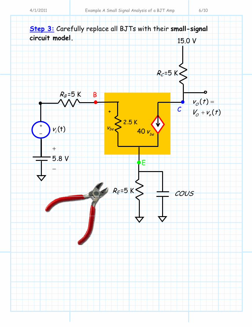
Step 3: Carefully replace all BJTs with their small-signal circuit model.
RB =5 K
RE =5 K COUS
15.0 V
RC =5 K
( )( )
O
oO
v tV v t
=
+
B
C
E
+ vbe
2 5 K.
40 bev (t)iv
5 8 V.+
−
+ _

4/1/2011 Example A Small Signal Analysis of a BJT Amp 7/10
Step 4: Set all D.C. sources to zero. We likewise notice that the large capacitor (COUS) is an approximate AC short, and thus we can further simplify the schematic by replacing it with a short circuit.
(t)iv
RB =5 K
RC =5 K
( )ov t
B
C
E
+ _
+ vbe
2 5 K.
40 bev
RE =5 K

4/1/2011 Example A Small Signal Analysis of a BJT Amp 8/10
We notice that one terminal of the small-signal voltage source, the emitter terminal, and one terminal of the collector resistor RC are all connected to ground—thus they are all collected to each other! We can use this fact to simplify the small-signal schematic.
(t)iv
RB =5 K
RC =5 K
( )ov t
B C
E
bi
ei
ci + vbe
2 5 K.
40 bev + _
4/1/2011 Example A Small Signal Analysis of a BJT Amp 9/10
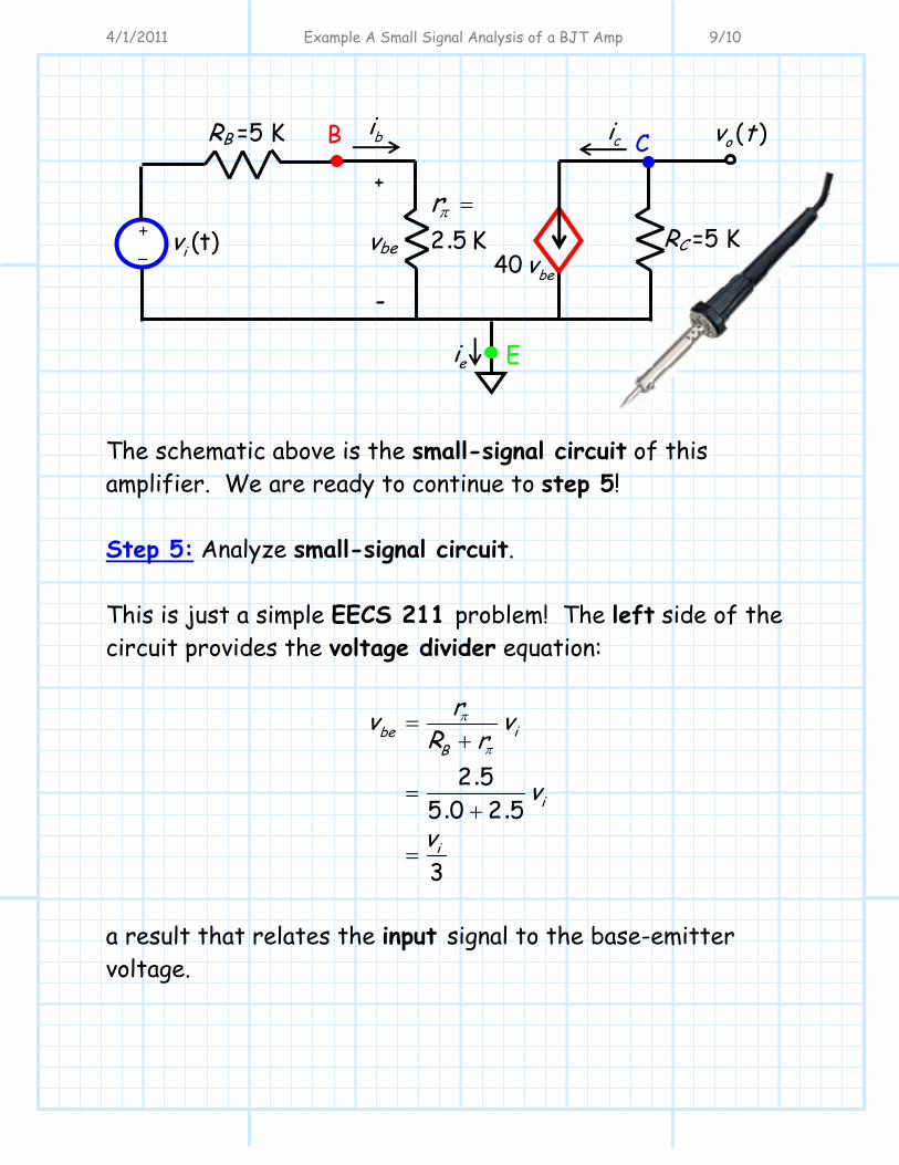
The schematic above is the small-signal circuit of this amplifier. We are ready to continue to step 5! Step 5: Analyze small-signal circuit. This is just a simple EECS 211 problem! The left side of the circuit provides the voltage divider equation:
2 55 0 2 5
3
.. .
ibeB
i
i
rv vR r
v
v
π
π
=+
=+
=
a result that relates the input signal to the base-emitter voltage.
bi ci
ei
+ _ (t)iv
RB =5 K
RC =5 K
( )ov t
+ vbe -
2 5 K.rπ =
40 bev
B C
E
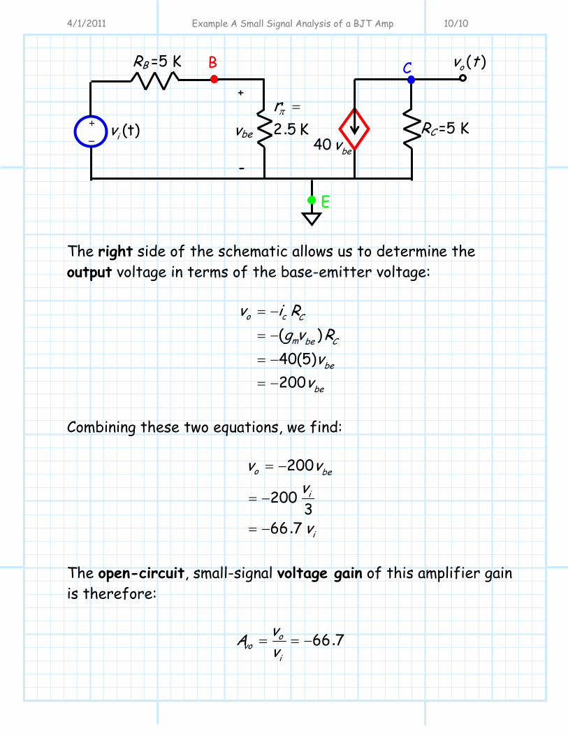
4/1/2011 Example A Small Signal Analysis of a BJT Amp 10/10
The right side of the schematic allows us to determine the output voltage in terms of the base-emitter voltage:
( )40(5)200
o c C
m be C
be
be
v i Rg v R
vv
= −
= −
= −
= −
Combining these two equations, we find:
200
2003
66 7.
o be
i
i
v vv
v
= −
= −
= −
The open-circuit, small-signal voltage gain of this amplifier gain is therefore:
66 7.ovo
i
vAv
= = −
+ _ (t)iv
RB =5 K
RC =5 K
( )ov t
+ vbe -
2 5 K.rπ =
40 bev
B C
E

4/4/2011 Example Small-Signal Input and Output Resistances 1/6
Example: Small-Signal Input and Output
Resistances Consider again this circuit: Recall we earlier determined the open-circuit voltage gain voA of this amplifier. But, recall also that voltage gain alone is not sufficient to characterize an amplifier—we likewise require the amplifier’s input and output resistances!
( ) ( )O O ov t V v t= +
+ _
15.0 V
( )iv t
5 8 V.+
−
RB =5 K
RC =5 K
RE =5 K COUS
100β =
4/4/2011 Example Small-Signal Input and Output Resistances 2/6
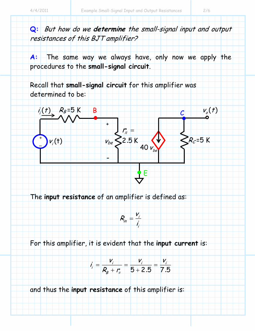
Q: But how do we determine the small-signal input and output resistances of this BJT amplifier? A: The same way we always have, only now we apply the procedures to the small-signal circuit.
Recall that small-signal circuit for this amplifier was determined to be: The input resistance of an amplifier is defined as:
iin
i
vRi
=
For this amplifier, it is evident that the input current is:
5 2 5 7 5. .i i i
iB
v v viR rπ
= = =+ +
and thus the input resistance of this amplifier is:
( )ii t
+ _ (t)iv
RB =5 K
RC =5 K
( )ov t
+ vbe -
2 5 K.rπ =
40 bev
B C
E
4/4/2011 Example Small-Signal Input and Output Resistances 3/6
7 5 K.iin
i
vRi
= =
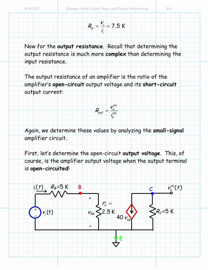
Now for the output resistance. Recall that determining the output resistance is much more complex than determining the input resistance. The output resistance of an amplifier is the ratio of the amplifier’s open-circuit output voltage and its short-circuit output current:
oco
out sco
vRi
=
Again, we determine these values by analyzing the small-signal amplifier circuit. First, let’s determine the open-circuit output voltage. This, of course, is the amplifier output voltage when the output terminal is open-circuited!
( )ii t
+ _ (t)iv
RB =5 K
RC =5 K
( )ocov t
+ vbe -
2 5 K.rπ =
40 bev
B C
E
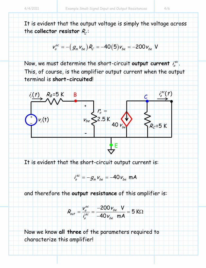
4/4/2011 Example Small-Signal Input and Output Resistances 4/6
It is evident that the output voltage is simply the voltage across the collector resistor CR :
( ) ( )40 5 200 Voco m be C be bev g v R v v= − = − = −
Now, we must determine the short-circuit output current sc
oi . This, of course, is the amplifier output current when the output terminal is short-circuited! It is evident that the short-circuit output current is:
40 mAsco m be bei g v v= − = −
and therefore the output resistance of this amplifier is:
200 V 5 K40 mA
ocbeo
out sco be
vvRi v
−= = = Ω
−
Now we know all three of the parameters required to characterize this amplifier!
RC =5 K + _ (t)iv
RB =5 K
+ vbe -
2 5 K.rπ =
40 bev
B C
E
( )ii t ( )scoi t
4/4/2011 Example Small-Signal Input and Output Resistances 5/6
66 7
7 5 K
5 0 K
vo
in
out
VA V
R
R
= −
= Ω
= Ω
.
.
.
We can therefore write the equivalent circuit model for this amplifier: Note that the input resistance of this amplifier is not particularly large, and output resistance is not at all small.
This is not a particularly good voltage amplifier!
7 5. K iv
+
−
ii
66.7 iv−
5.0K
ov+
−
oi
+
−

4/4/2011 Example Small-Signal Input and Output Resistances 6/6
Now, reflect on how far we have come. We began with the amplifier circuit: and now we have derived its equivalent small-signal circuit: With respect to small signal input/output voltages and currents, these two circuits are precisely the same!
( ) ( )O O ov t V v t= +
+ _
15.0 V
( )iv t
5 8 V.+
−
RB =5 K
RC =5 K
RE =5 K COUS
100β =
7 5. K 66.7 iv−
5.0K ov
+
− +
_ ( )iv t
ii