Embed Size (px)
Citation preview

HopeRF's RFM22B/23B are highly integrated, low cost,433/868/915MHZwireless ISM transceivers module. The low receive sensitivity
coupled with industry leading +20dBm output power ensures
range and improved link performance. Built-in antenna diversity andsupport for frequency hopping can be used to further extend range and enhance
performance.
Additional system features such as an automatic wake-up timer, low
battery detector, 64 byte TX/RX FIFOs, automatic packet handling, and preambledetection reduce overall current consumption and allow the use of lower-cost
system MCUs. An integrated temperature sensor, general purpose ADC, power-
on-reset (POR), and GPIOs further reduce overall system cost and size.The RFM22B/23B’s digital receive architecture features a high-performance ADC
and DSP based modem which performs demodulation, filtering, and packet
handling for increased flexibility and performance. The direct digital transmitmodulation and automatic PA power ramping ensure precise transmit modulation
and reduced spectral spreading ensuring compliance with global regulations
including FCC, ETSI.An easy-to-use calculator is provided to quickly configure the radio settings,
simplifying customer's system design and reducing time to market.
Frequency Range
433/868/915MHz ISM bands
Sensitivity = –121 dBm Output power range
+20 dBm Max (RFM22B)
+13 dBm Max (RFM23B)
Low Power Consumption18.5 mA receive30 mA @ +13 dBm transmit85 mA @ +20 dBm transmit
Data Rate = 0.123 to 256 kbpsFSK, GFSK, and OOK modulationPower Supply = 1.8 to 3.6 VUltra low power shutdown modeDigital RSSI
Wake-up timer
Auto-frequency calibration (AFC)
Power-on-reset (POR)Antenna diversity and TR switch controlConfigurable packet handlerPreamble detectorTX and RX 64 byte FIFOsLow battery detector Temperature sensor and 8-bit ADC–40 to +85 °C temperature rangeIntegrated voltage regulatorsFrequency hopping capabilityOn-chip crystal tuning14-PIN DIP & 16-PIN SMD packageLow cost
Remote controlHome security & alarmTelemetryPersonal data loggingToy controlTire pressure monitoringWireless PC peripherals
Remote meter readingRemote keyless entryHome automationIndustrial controlSensor networksHealth monitorsTag readers
Tel: +86-755-82973805 Fax: +86-755-82973550 E-mail: [email protected] http://www.hoperf.com
V1.0
1
(–121dBm)extended
2.1. Operating Modes . . . . . . . . . . . . . . . . . . . . . . . . . . . . . . . . . . . . . . . . . . . . . . . . . . . .13
3.1. Serial Peripheral Interface (SPI) . . . . . . . . . . . . . . . . . . . . . . . . . . . . . . . . . . . . . . . .143.2. Operating Mode Control . . . . . . . . . . . . . . . . . . . . . . . . . . . . . . . . . . . . . . . . . . . . . .163.3. Interrupts . . . . . . . . . . . . . . . . . . . . . . . . . . . . . . . . . . . . . . . . . . . . . . . . . . . . . . . . .193.4. System Timing . . . . . . . . . . . . . . . . . . . . . . . . . . . . . . . . . . . . . . . . . . . . . . . . . . . . .203.5. Frequency Control . . . . . . . . . . . . . . . . . . . . . . . . . . . . . . . . . . . . . . . . . . . . . . . . . . .21
4.1. Modulation Type . . . . . . . . . . . . . . . . . . . . . . . . . . . . . . . . . . . . . . . . . . . . . . . . . . . .284.2. Modulation Data Source . . . . . . . . . . . . . . . . . . . . . . . . . . . . . . . . . . . . . . . . . . . . . .29
5.1. RX LNA . . . . . . . . . . . . . . . . . . . . . . . . . . . . . . . . . . . . . . . . . . . . . . . . . . . . . . . . . . .335.2. RX I-Q Mixer . . . . . . . . . . . . . . . . . . . . . . . . . . . . . . . . . . . . . . . . . . . . . . . . . . . . . . .335.3. Programmable Gain Amplifier . . . . . . . . . . . . . . . . . . . . . . . . . . . . . . . . . . . . . . . . . .335.4. ADC . . . . . . . . . . . . . . . . . . . . . . . . . . . . . . . . . . . . . . . . . . . . . . . . . . . . . . . . . . . . . .335.5. Digital Modem . . . . . . . . . . . . . . . . . . . . . . . . . . . . . . . . . . . . . . . . . . . . . . . . . . . . . .335.6. Synthesizer . . . . . . . . . . . . . . . . . . . . . . . . . . . . . . . . . . . . . . . . . . . . . . . . . . . . . . . .345.7. Power Amplifier . . . . . . . . . . . . . . . . . . . . . . . . . . . . . . . . . . . . . . . . . . . . . . . . . . . . .355.8. Crystal Oscillator . . . . . . . . . . . . . . . . . . . . . . . . . . . . . . . . . . . . . . . . . . . . . . . . . . . .365.9. Regulators . . . . . . . . . . . . . . . . . . . . . . . . . . . . . . . . . . . . . . . . . . . . . . . . . . . . . . . . .36
6.1. RX and TX FIFOs . . . . . . . . . . . . . . . . . . . . . . . . . . . . . . . . . . . . . . . . . . . . . . . . . . .376.2. Packet Configuration . . . . . . . . . . . . . . . . . . . . . . . . . . . . . . . . . . . . . . . . . . . . . . . . .386.3. Packet Handler TX Mode . . . . . . . . . . . . . . . . . . . . . . . . . . . . . . . . . . . . . . . . . . . . .396.4. Packet Handler RX Mode . . . . . . . . . . . . . . . . . . . . . . . . . . . . . . . . . . . . . . . . . . . . .396.5. Data Whitening, Manchester Encoding, and CRC . . . . . . . . . . . . . . . . . . . . . . . . . .426.6. Preamble Detector . . . . . . . . . . . . . . . . . . . . . . . . . . . . . . . . . . . . . . . . . . . . . . . . . .426.7. Preamble Length . . . . . . . . . . . . . . . . . . . . . . . . . . . . . . . . . . . . . . . . . . . . . . . . . . . .436.8. Invalid Preamble Detector . . . . . . . . . . . . . . . . . . . . . . . . . . . . . . . . . . . . . . . . . . . . .436.9. Synchronization Word Configuration . . . . . . . . . . . . . . . . . . . . . . . . . . . . . . . . . . . . .436.10. Receive Header Check . . . . . . . . . . . . . . . . . . . . . . . . . . . . . . . . . . . . . . . . . . . . . .446.11. TX Retransmission and Auto TX . . . . . . . . . . . . . . . . . . . . . . . . . . . . . . . . . . . . . . .44
7.1. Modem Settings for FSK and GFSK . . . . . . . . . . . . . . . . . . . . . . . . . . . . . . . . . . . . .45
8.1. Smart Reset . . . . . . . . . . . . . . . . . . . . . . . . . . . . . . . . . . . . . . . . . . . . . . . . . . . . . . .46
Tel: +86-755-82973805 Fax: +86-755-82973550 E-mail: [email protected] http://www.hoperf.com

8.2. Microcontroller Clock . . . . . . . . . . . . . . . . . . . . . . . . . . . . . . . . . . . . . . . . . . . . . . . . .478.3. General Purpose ADC . . . . . . . . . . . . . . . . . . . . . . . . . . . . . . . . . . . . . . . . . . . . . . .488.4. Temperature Sensor . . . . . . . . . . . . . . . . . . . . . . . . . . . . . . . . . . . . . . . . . . . . . . . . .498.5. Low Battery Detector . . . . . . . . . . . . . . . . . . . . . . . . . . . . . . . . . . . . . . . . . . . . . . . . .518.6. Wake-Up Timer and 32 kHz Clock Source . . . . . . . . . . . . . . . . . . . . . . . . . . . . . . . .528.7. Low Duty Cycle Mode . . . . . . . . . . . . . . . . . . . . . . . . . . . . . . . . . . . . . . . . . . . . . . . .548.8. GPIO Configuration . . . . . . . . . . . . . . . . . . . . . . . . . . . . . . . . . . . . . . . . . . . . . . . . . .558.9. Antenna Diversity . . . . . . . . . . . . . . . . . . . . . . . . . . . . . . . . . . . . . . . . . . . . . . . . . . .568.10. RSSI and Clear Channel Assessment . . . . . . . . . . . . . . . . . . . . . . . . . . . . . . . . . .57
Tel: +86-755-82973805 Fax: +86-755-82973550 E-mail: [email protected] http://www.hoperf.com
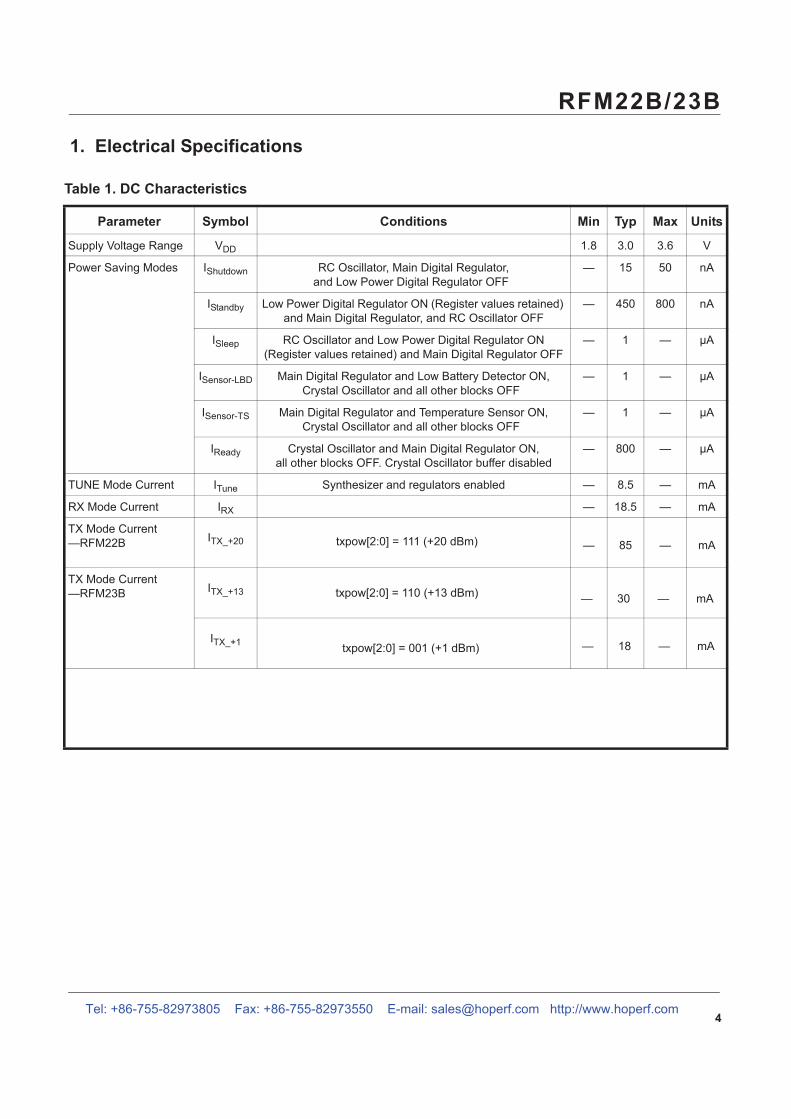
Supply Voltage Range VDD 1.8 3.0 3.6 V
Power Saving Modes IShutdown RC Oscillator, Main Digital Regulator,
and Low Power Digital Regulator OFF
— 15 50 nA
IStandby Low Power Digital Regulator ON (Register values retained)
and Main Digital Regulator, and RC Oscillator OFF
— 450 800 nA
ISleep RC Oscillator and Low Power Digital Regulator ON
(Register values retained) and Main Digital Regulator OFF
— 1 — µA
ISensor-LBD Main Digital Regulator and Low Battery Detector ON,
Crystal Oscillator and all other blocks OFF
— 1 — µA
ISensor-TS Main Digital Regulator and Temperature Sensor ON,
Crystal Oscillator and all other blocks OFF
— 1 — µA
IReady Crystal Oscillator and Main Digital Regulator ON,
all other blocks OFF. Crystal Oscillator buffer disabled
— 800 — µA
TUNE Mode Current ITune Synthesizer and regulators enabled — 8.5 — mA
RX Mode Current IRX — 18.5 — mA
TX Mode Current
—RFM22BITX_+20 txpow[2:0] = 111 (+20 dBm) — 85 — mA
TX Mode Current
—RFM23BITX_+13 txpow[2:0] = 110 (+13 dBm)
— 30 — mA
ITX_+1txpow[2:0] = 001 (+1 dBm) — 18 — mA
Tel: +86-755-82973805 Fax: +86-755-82973550 E-mail: [email protected] http://www.hoperf.com

Synthesizer Frequency
Range—RFM22B/23BFSYN 848 888 MHz
Synthesizer Frequency
Resolution
FRES-LB 433MHz Band — 156.25 — Hz
FRES-HB 868/915MHz Band — 312.5 — Hz
Reference Frequency
Input Level
fREF_LV When using external reference signal
driving XOUT pin, instead of using
crystal. Measured peak-to-peak (VPP)
0.7 — 1.6 V
Synthesizer Settling Time tLOCK Measured from exiting Ready mode with
XOSC running to any frequency.
Including VCO Calibration.
— 200 — µs
Residual FM FRMS Integrated over 250 kHz bandwidth
(500 Hz lower bound of integration)
— 2 4 kHzRMS
Phase Noise L (fM) F = 10 kHz — –80 — dBc/Hz
F = 100 kHz — –90 — dBc/Hz
F = 1 MHz — –115 — dBc/Hz
F = 10 MHz — –130 — dBc/Hz
Tel: +86-755-82973805 Fax: +86-755-82973550 E-mail: [email protected] http://www.hoperf.com
413 453 MHz
901 929 MHz
433MHz band
868MHz band
915MHz band

RX Frequency
Range—RFM22B/23B FRX
RX Sensitivity PRX_2 (BER < 0.1%)
(2 kbps, GFSK, BT = 0.5,
— –121 — dBm
PRX_40 (BER < 0.1%)
(1.2 kbps, FSK, BT=0.5,
f = 45kHz)
— –114 — dBm
PRX_100 (BER < 0.1%)
(100 kbps, GFSK, BT = 0.5,
f = 50 kHz)
— –104 — dBm
PRX_125 (BER < 0.1%)
(125 kbps, GFSK, BT = 0.5,
f = 62.5 kHz)
— –101 — dBm
PRX_OOK (BER < 0.1%)
(4.8 kbps, 350 kHz BW, OOK)
— –110 — dBm
(BER < 0.1%)
(40 kbps, 400 kHz BW, OOK)
— –102 — dBm
RX Channel Bandwidth BW 2.6 — 620 kHz
BER Variation vs Power
LevelPRX_RES Up to +5 dBm Input Level — 0 0.1 ppm
RSSI Resolution RESRSSI — ±0.5 — dB
1-Ch Offset Selectivity C/I1-CH Desired Ref Signal 3 dB above sensitivity,
BER < 0.1%. Interferer and desired modu-
lated with 40 kbps F = 20 kHz GFSK with
BT = 0.5, channel spacing = 150 kHz
— –31 — dB
2-Ch Offset Selectivity C/I2-CH — –35 — dB
3-Ch Offset Selectivity C/I3-CH — –40 — dB
Blocking at 1 MHz Offset 1MBLOCK Desired Ref Signal 3 dB above sensitivity.
Interferer and desired modulated with
40 kbps F = 20 kHz GFSK with BT = 0.5
— –52 — dB
Blocking at 4 MHz Offset 4MBLOCK — –56 — dB
Blocking at 8 MHz Offset 8MBLOCK — –63 — dB
Image Rejection ImREJ Rejection at the image frequency.
IF=937 kHz
— –30 — dB
Spurious Emissions POB_RX1 Measured at RX pins — — –54 dBm
Tel: +86-755-82973805 Fax: +86-755-82973550 E-mail: [email protected] http://www.hoperf.com
433MHz band
868MHz band
915MHz band
848 888 MHz
413 453 MHz
895 935 MHz
f = 5 kHz)special crystal is used on the module

TX Frequency
Range—RFM22B/23BFTX
FSK Data Rate DRFSK 0.123 — 256 kbps
OOK Data Rate DROOK 0.123 — 40 kbps
Modulation Deviation f1 868/915MHz ±0.625 ±320 kHz
f2 433MHz ±0.625 ±160 kHz
Modulation Deviation
Resolution
fRES — 0.625 — kHz
Output Power
Range—RFM22B
PTX +1 — +20 dBm
Output Power
Range—RFM23B
PTX –8 — +13 dBm
TX RF Output Steps PRF_OUT controlled by txpow[2:0] — 3 — dB
TX RF Output Level
Variation vs. Temperature
PRF_TEMP –40 to +85 C — 2 — dB
TX RF Output Level
Variation vs. Frequency
PRF_FREQ Measured across any one
frequency band
— 1 — dB
Transmit Modulation
Filtering
B*T Gaussian Filtering Bandwith Time
Product
— 0.5 —
Spurious EmissionsPOB-TX1 POUT = +13 dBm,
Frequencies <1 GHz
— — –54 dBm
POB-TX2 1–12.75 GHz, excluding harmonics — — –54 dBm
Tel: +86-755-82973805 Fax: +86-755-82973550 E-mail: [email protected] http://www.hoperf.com
433MHz band
868MHz band
915MHz band
848 888 MHz
413 453 MHz
895 935 MHz

Temperature Sensor
Accuracy
TSA After calibrated via sensor offset
register tvoffs[7:0]
— 0.5 — °C
Temperature Sensor
Sensitivity
TSS — 5 — mV/°C
Low Battery Detector
Resolution
LBDRES — 50 — mV
Low Battery Detector
Conversion Time
LBDCT — 250 — µs
Microcontroller Clock
Output Frequency
FMC Configurable to 30 MHz,
15 MHz, 10 MHz, 4 MHz,
3 MHz, 2 MHz, 1 MHz, or
32.768 kHz
32.768K — 30M Hz
General Purpose ADC
Resolution
ADCENB — 8 — bit
General Purpose ADC Bit
Resolution
ADCRES — 4 — mV/bit
Temp Sensor & General
Purpose ADC Conversion
Time
ADCCT — 305 — µs
30 MHz XTAL Start-Up time t30M — 600 — µs
30 MHz XTAL Cap
Resolution
30MRES — 97 — fF
32 kHz XTAL Start-Up Time t32k — 6 — sec
32 kHz XTAL Accuracy
using 32 kHz XTAL
32KRES — 100 — ppm
32 kHz Accuracy using
Internal RC Oscillator
32KRCRES — 2500 — ppm
POR Reset Time tPOR — 16 — ms
Software Reset Time tsoft — 100 — µs
Tel: +86-755-82973805 Fax: +86-755-82973550 E-mail: [email protected] http://www.hoperf.com
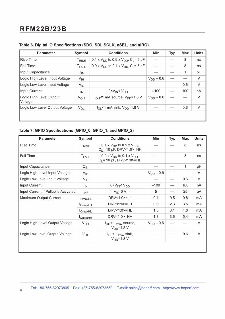
Rise Time TRISE 0.1 x VDD to 0.9 x VDD, CL= 5 pF — — 8 ns
Fall Time TFALL 0.9 x VDD to 0.1 x VDD, CL= 5 pF — — 8 ns
Input Capacitance CIN — — 1 pF
Logic High Level Input Voltage VIH VDD – 0.6 — — V
Logic Low Level Input Voltage VIL — 0.6 V
Input Current IIN 0<VIN< VDD –100 — 100 nA
Logic High Level Output
Voltage
VOH IOH<1 mA source, VDD=1.8 V VDD – 0.6 — — V
Logic Low Level Output Voltage VOL IOL<1 mA sink, VDD=1.8 V — — 0.6 V
Rise Time TRISE 0.1 x VDD to 0.9 x VDD,
CL= 10 pF, DRV<1:0>=HH
— — 8 ns
Fall Time TFALL 0.9 x VDD to 0.1 x VDD,
CL= 10 pF, DRV<1:0>=HH
— — 8 ns
Input Capacitance CIN — — 1 pF
Logic High Level Input Voltage VIH VDD – 0.6 — V
Logic Low Level Input Voltage VIL — — 0.6 V
Input Current IIN 0<VIN< VDD –100 — 100 nA
Input Current If Pullup is Activated IINP VIL=0 V 5 — 25 µA
Maximum Output Current IOmaxLL DRV<1:0>=LL 0.1 0.5 0.8 mA
IOmaxLH DRV<1:0>=LH 0.9 2.3 3.5 mA
IOmaxHL DRV<1:0>=HL 1.5 3.1 4.8 mA
IOmaxHH DRV<1:0>=HH 1.8 3.6 5.4 mA
Logic High Level Output Voltage VOH IOH< IOmax source,
VDD=1.8 V
VDD – 0.6 — — V
Logic Low Level Output Voltage VOL IOL< IOmax sink,
VDD=1.8 V
— — 0.6 V
Tel: +86-755-82973805 Fax: +86-755-82973550 E-mail: [email protected] http://www.hoperf.com

VDD to GND –0.3, +3.6 V
Instantaneous VRF-peak to GND on TX Output Pin –0.3, +8.0 V
Sustained VRF-peak to GND on TX Output Pin –0.3, +6.5 V
Voltage on Digital Control Inputs –0.3, VDD + 0.3 V
Voltage on Analog Inputs –0.3, VDD + 0.3 V
RX Input Power +10 dBm
Operating Temperature Range (Normal crystal is used on the module) T N
–40 to +85 C
Thermal Impedance JA 30 C/W
Storage Temperature Range TSTG –55 to +125 C
Stresses beyond those listed under “Absolute Maximum Ratings” may cause permanent damage to the device. These
are stress ratings only and functional operation of the device at or beyond these ratings in the operational sections of
the specifications is not implied. Exposure to absolute maximum rating conditions for extended periods may affect
device reliability. Power Amplifier may be damaged if switched on without proper load or termination connected. TX
matching network design will influence TX VRF-peak on TX output pin. Caution: ESD sensitive device.
Tel: +86-755-82973805 Fax: +86-755-82973550 E-mail: [email protected] http://www.hoperf.com
S
–20 to +60 C
Operating Temperature Range (special crystal is used on the module) T

The wide operating voltage range of 1.8–3.6 V and low current consumption
an ideal solution for battery powered applications.
The RFM22B/23B operates as a time division duplexing (TDD) transceiver where the device alternately transmits
and receives data packets. The device uses a single-conversion mixer to downconvert the 2-level FSK/GFSK/OOK
modulated receive signal to a low IF frequency. Following a programmable gain amplifier (PGA) the signal is
converted to the digital domain by a high performance ADC allowing filtering, demodulation, slicing, and packet
handling to be performed in the built-in DSP increasing the receiver’s performance and flexibility versus analog
based architectures. The demodulated signal is then output to the system MCU through a programmable GPIO or
via the standard SPI bus by reading the 64-byte RX FIFO.
A single high precision local oscillator (LO) is used for both transmit and receive modes since the transmitter and
receiver do not operate at the same time. The LO is generated by an integrated VCO and Fractional-N PLL
synthesizer. The synthesizer is designed to support configurable data rates, output frequency and frequency
deviation at 433MHz,868MHz,915MHz band. The transmit FSK data is modulated directly into the data
stream and can be shaped by a Gaussian low-pass filter to reduce unwanted spectral content.
The RFM22B’s PA output power can be configured between +1 and +20 dBm in 3 dB steps, while the RFM23B's
PA output power can be configured between –8 and +13 dBm in 3 dB steps. The RFM22B/23B supports
frequency hopping, TX/RX switch control, and antenna diversity switch control to extend the link range and
The RFM22B/23B is designed to work with a microcontroller to create a very low cost system as shown
tors are integrated on-chip which allows for a wide
from +1.8 to +3.6 V. A standard 4-pin SPI bus is used to communicate with an
configurable general purpose I/Os are available. A complete list of the available
"8. Auxiliary Functions"and includes microcontroller clock output, Antenna Diversity, POR, and various interrupts.
Tel: +86-755-82973805 Fax: +86-755-82973550 E-mail: [email protected] http://www.hoperf.com
HopeRF's RFM22B/23B are highly integrated,low cost,433/868/915MHz wireless ISM transceivers module .makes theRFM22B/23B
improve performance
Figure 1. Voltage regula operating supply voltage range
external microcontroller. Three
GPIO functions is shown in

X1
30MHz
microcontroller
VDD
VSS
GP1
GP2
GP3
GP4
100n
C7
100p
C8
C1
L1
L3
L2
C6
C3 C2
1u
VDD_RF SCLK19
18
17
16
1
2
3
4
15
14
13
7 8 9 10
SDI
SDO
VDD_DRXn
TX
RFp
GP
IO0
GP
IO1
VR
_D
IG
nIR
Q
SD
N
XO
UT
nS
EL
GP
IO2
5NC
6A
NT
1
NC
20
XIN
11
12
GP5
C9
1u
L5
C5
C4
L4
L6
Tel: +86-755-82973805 Fax: +86-755-82973550 E-mail: [email protected] http://www.hoperf.com
RFM23B MODULE

The RFM22B/23B provides several operating modes which can be used to optimize the power consumption for a
given application. Depending upon the system communication protocol, an optimal trade-off between the radio
wake time and power consumption can be achieved.
Table 9 summarizes the operating modes of the RFM22B/23B. In general, any given operating mode may be
classified as an active mode or a power saving mode. The table indicates which block(s) are enabled (active) in
each corresponding mode. With the exception of the SHUTDOWN mode, all can be dynamically selected by
sending the appropriate commands over the SPI. An “X” in any cell means that, in the given mode of operation,
that block can be independently programmed to be either ON or OFF, without noticeably impacting the current
consumption. The SPI circuit block includes the SPI interface hardware and the device register space. The 32 kHz
OSC block includes the 32.768 kHz RC oscillator or 32.768 kHz crystal oscillator and wake-up timer. AUX
(Auxiliary Blocks) includes the temperature sensor, general purpose ADC, and low-battery detector.
SHUT-
DOWN
OFF (Register
contents lost)
OFF OFF OFF OFF OFF OFF OFF 15 nA
STANDBY ON (Register
contents
retained)
ON OFF OFF OFF OFF OFF OFF 450 nA
SLEEP ON ON X OFF OFF OFF OFF 1 µA
SENSOR ON X ON OFF OFF OFF OFF 1 µA
READY ON X X ON OFF OFF OFF 800 µA
TUNING ON X X ON ON OFF OFF 8.5 mA
TRANSMIT ON X X ON ON ON OFF 30 mA*
RECEIVE ON X X ON ON OFF ON 18.5 mA
Using RFM23B at +13 dBm using recommended reference design.
Tel: +86-755-82973805 Fax: +86-755-82973550 E-mail: [email protected] http://www.hoperf.com

The RFM22B/23B communicates with the host MCU over a standard 3-wire SPI interface: SCLK, SDI, and nSEL.
The host MCU can read data from the device on the SDO output pin. A SPI transaction is a 16-bit sequence which
consists of a Read-Write (R/W) select bit, followed by a 7-bit address field (ADDR), and an 8-bit data field (DATA)
as demonstrated in Figure 3. The 7-bit address field is used to select one of the 128, 8-bit control registers. The
R/W select bit determines whether the SPI transaction is a read or write transaction. If R/W = 1 it signifies a WRITE
transaction, while R/W = 0 signifies a READ transaction. The contents (ADDR or DATA) are latched into the
RFM22B/23B every eight clock cycles. The timing parameters for the SPI interface are shown in Table 10. The
SCLK rate is flexible with a maximum rate of 10 MHz.
To read back data from the RFM22B/23B, the R/W bit must be set to 0 followed by the 7-bit address of the register
from which to read. The 8 bit DATA field following the 7-bit ADDR field is ignored on the SDI pin when R/W = 0. The
next eight negative edge transitions of the SCLK signal will clock out the contents of the selected register. The data
read from the selected register will be available on the SDO output pin. The READ function is shown in Figure 4.
After the READ function is completed the SDO pin will remain at either a logic 1 or logic 0 state depending on the
last data bit clocked out (D0). When nSEL goes high the SDO output pin will be pulled high by internal pullup.
tCH Clock high time 40
tCL Clock low time 40
tDS Data setup time 20
tDH Data hold time 20
tDD Output data delay time 20
tEN Output enable time 20
tDE Output disable time 50
tSS Select setup time 20
tSH Select hold time 50
tSW Select high period 80
SDI
SCLK
SDO
nSEL
tCL tCH tDS tDH tDDtSS
tEN
tSH tDE
tSW
Tel: +86-755-82973805 Fax: +86-755-82973550 E-mail: [email protected] http://www.hoperf.com

The SPI interface contains a burst read/write mode which allows for reading/writing sequential registers without
having to re-send the SPI address. When the nSEL bit is held low while continuing to send SCLK pulses, the SPI
interface will automatically increment the ADDR and read from/write to the next address. An example burst write
transaction is illustrated in Figure 5 and a burst read in Figure 6. As long as nSEL is held low, input data will be
latched into the RFM22B/23B every eight SCLK cycles.
Tel: +86-755-82973805 Fax: +86-755-82973550 E-mail: [email protected] http://www.hoperf.com

There are four primary states in the RFM22B/23B radio state machine: SHUTDOWN, IDLE, TX, and RX (see
Figure 7). The SHUTDOWN state completely shuts down the radio to minimize current consumption. There are five
different configurations/options for the IDLE state which can be selected to optimize the chip to the applications
needs. "Register 07h. Operating Mode and Function Control 1" controls which operating mode/state is selected
with the exception of SHUTDOWN which is controlled by SDN pin 20. The TX and RX state may be reached
automatically from any of the IDLE states by setting the txon/rxon bits in "Register 07h. Operating Mode and
Function Control 1". Table 11 shows each of the operating modes with the time required to reach either RX or TX
mode as well as the current consumption of each mode.
The RFM22B/23B includes a low-power digital regulated supply (LPLDO) which is internally connected in parallel
to the output of the main digital regulator (and is available externally at the VR_DIG pin). This common digital
supply voltage is connected to all digital circuit blocks including the digital modem, crystal oscillator, SPI, and
register space. The LPLDO has extremely low quiescent current consumption but limited current supply capability;
it is used only in the IDLE-STANDBY and IDLE-SLEEP modes. The main digital regulator is automatically enabled
in all other modes.
Shut Down State 16.8 ms 16.8 ms 15 nA
Idle States:
Standby Mode
Sleep Mode
Sensor Mode
Ready Mode
Tune Mode
800 µs
800 µs
800 µs
200 µs
200 µs
800 µs
800 µs
800 µs
200 µs
200 µs
450 nA
1 µA
1 µA
800 µA
8.5 mA
TX State NA 200 µs 30 mA @ +13 dBm
RX State 200 µs NA 18.5 mA
*Five Different Options for IDLE
SHUTDOWN
Tel: +86-755-82973805 Fax: +86-755-82973550 E-mail: [email protected] http://www.hoperf.com

The SHUTDOWN state is the lowest current consumption state of the device with nominally less than 15 nA of
current consumption. The shutdown state may be entered by driving the SDN pin high. The SDN pin
should be held low in all states except the SHUTDOWN state. In the SHUTDOWN state, the contents of the
registers are lost and there is no SPI access.
When the chip is connected to the power supply, a POR will be initiated after the falling edge of SDN.
There are five different modes in the IDLE state which may be selected by "Register 07h. Operating Mode and
Function Control 1". All modes have a tradeoff between current consumption and response time to TX/RX mode.
This tradeoff is shown in Table 11. After the POR event, SWRESET, or exiting from the SHUTDOWN state the chip
will default to the IDLE-READY mode. After a POR event the interrupt registers must be read to properly enter the
SLEEP, SENSOR, or STANDBY mode and to control the 32 kHz clock correctly.
STANDBY mode has the lowest current consumption of the five IDLE states with only the LPLDO enabled to
maintain the register values. In this mode the registers can be accessed in both read and write mode. The
STANDBY mode can be entered by writing 0h to "Register 07h. Operating Mode and Function Control 1". If an
interrupt has occurred (i.e., the nIRQ pin = 0) the interrupt registers must be read to achieve the minimum current
consumption. Additionally, the ADC should not be selected as an input to the GPIO in this mode as it will cause
excess current consumption.
In SLEEP mode the LPLDO is enabled along with the Wake-Up-Timer, which can be used to accurately wake-up
the radio at specified intervals. See "8.6. Wake-Up Timer and 32 kHz Clock Source for more
on the Wake -Up-Timer. SLEEP mode is entered by setting enwt = 1 (40h) in "Register 07h. Operating
Mode and Function Control 1". If an interrupt has occurred (i.e., the nIRQ pin = 0) the interrupt registers must be
read to achieve the minimum current consumption. Also, the ADC should not be selected as an input to the GPIO
in this mode as it will cause excess current consumption.
In SENSOR mode either the Low Battery Detector, Temperature Sensor, or both may be enabled in addition to the
LPLDO and Wake-Up-Timer. The Low Battery Detector can be enabled by setting enlbd = 1 in "Register 07h.
Operating Mode and Function Control 1". See "8.4. Temperature Sensor" and "8.5. Low Battery
Detector" for more information on these features. If an interrupt has occurred (i.e., the nIRQ pin = 0)
the interrupt registers must be read to achieve the minimum current consumption.
READY Mode is designed to give a fast transition time to TX mode with reasonable current consumption. In this
mode the Crystal oscillator remains enabled reducing the time required to switch to TX or RX mode by eliminating
the crystal start-up time. READY mode is entered by setting xton = 1 in "Register 07h. Operating Mode and
Function Control 1". To achieve the lowest current consumption state the crystal oscillator buffer should be
disabled in “Register 62h. Crystal Oscillator Control and Test.” To exit READY mode, bufovr (bit 1) of this register
must be set back to 0.
In TUNE mode the PLL remains enabled in addition to the other blocks enabled in the IDLE modes. This will give
the fastest response to TX mode as the PLL will remain locked but it results in the highest current consumption.
This mode of operation is designed for frequency hopping spread spectrum systems (FHSS). TUNE mode is
entered by setting pllon = 1 in "Register 07h. Operating Mode and Function Control 1". It is not necessary to set
xton to 1 for this mode, the internal state machine automatically enables the crystal oscillator.
Tel: +86-755-82973805 Fax: +86-755-82973550 E-mail: [email protected] http://www.hoperf.com
information

The TX state may be entered from any of the IDLE modes when the txon bit is set to 1 in "Register 07h. Operating
Mode and Function Control 1". A built-in sequencer takes care of all the actions required to transition between
states from enabling the crystal oscillator to ramping up the PA. The following sequence of events will occur
automatically when going from STANDBY mode to TX mode by setting the txon bit.
1. Enable the main digital LDO and the Analog LDOs.
2. Start up crystal oscillator and wait until ready (controlled byan internal timer).
3. Enable PLL.
4. Calibrate VCO (this action is skipped when the vcocal bit is “0”, default value is “1”).
5. Wait until PLL settles to required transmit frequency (controlled by an internal timer).
6. Activate power amplifier and wait until power ramping is completed (controlled by an internal timer).
7. Transmit packet.
Steps in this sequence may be eliminated depending on which IDLE mode the chip is configured to prior to setting
the txon bit. By default, the VCO and PLL are calibrated every time the PLL is enabled.
The RX state may be entered from any of the IDLE modes when the rxon bit is set to 1 in "Register 07h. Operating
Mode and Function Control 1". A built-in sequencer takes care of all the actions required to transition from one of
the IDLE modes to the RX state. The following sequence of events will occur automatically to get the chip into RX
mode when going from STANDBY mode to RX mode by setting the rxon bit:
1. Enable the main digital LDO and the Analog LDOs.
2. Start up crystal oscillator and wait until ready (controlled by an internal timer).
3. Enable PLL.
4. Calibrate VCO (this action is skipped when the vcocal bit is “0”, default value is “1”).
5. Wait until PLL settles to required receive frequency (controlled by an internal timer).
6. Enable receive circuits: LNA, mixers, and ADC.
7. Enable receive mode in the digital modem.
Depending on the configuration of the radio all or some of the following functions will be performed automatically by
the digital modem: AGC, AFC (optional), update status registers, bit synchronization, packet handling (optional)
including sync word, header check, and CRC.
The operational status of the chip can be read from "Register 02h. Device Status".
02 R Device Status ffovfl ffunfl rxffem headerr freqerr cps[1] cps[0] —
Tel: +86-755-82973805 Fax: +86-755-82973550 E-mail: [email protected] http://www.hoperf.com

The RFM22B/23B is capable of generating an interrupt signal when certain events occur. The chip notifies the
microcontroller that an interrupt event has occurred by setting the nIRQ output pin LOW = 0. This interrupt signal
will be generated when any one (or more) of the interrupt events (corresponding to the Interrupt Status bits) shown
below occur. The nIRQ pin will remain low until the microcontroller reads the Interrupt Status Register(s) (Registers
03h–04h) containing the active Interrupt Status bit. The nIRQ output signal will then be reset until the next change
in status is detected. The interrupts must be enabled by the corresponding enable bit in the Interrupt Enable
Registers (Registers 05h–06h). All enabled interrupt bits will be cleared when the microcontroller reads the
interrupt status register. If the interrupt is not enabled when the event occurs it will not trigger the nIRQ pin, but the
status may still be read at anytime in the Interrupt Status registers.
03 R Interrupt Status 1 ifferr itxffafull itxffaem irxffafull iext ipksent ipkvalid icrcerror —
04 R Interrupt Status 2 iswdet ipreaval ipreainval irssi iwut ilbd ichiprdy ipor —
05 R/W Interrupt Enable 1 enfferr entxffafull entxffaem enrxffafull enext enpksent enpkvalid encrcerror 00h
06 R/W Interrupt Enable 2 enswdet enpreaval enpreainval enrssi enwut enlbd enchiprdy enpor 01h
Tel: +86-755-82973805 Fax: +86-755-82973550 E-mail: [email protected] http://www.hoperf.com

The system timing for TX and RX modes is shown in Figures 8 and 9. The figures demonstrate transitioning from
STANDBY mode to TX or RX mode through the built-in sequencer of required steps. The user only needs to
program the desired mode, and the internal sequencer will properly transition the part from its current mode.
The VCO will automatically calibrate at every frequency change or power up. The PLL T0 time is to allow for bias
settling of the VCO. The PLL TS time is for the settling time of the PLL, which has a default setting of 100 µs. The
total time for PLL T0, PLL CAL, and PLL TS under all conditions is 200 µs. Under certain applications, the PLL T0
time and the PLL CAL may be skipped for faster turn-around time. Contact applications support if faster turnaround
time is desired.
Tel: +86-755-82973805 Fax: +86-755-82973550 E-mail: [email protected] http://www.hoperf.com

For calculating the necessary frequency register settings it is recommended that customers use
the HOPERF Register Calculator worksheet (in Microsoft Excel) available on
These methods offer a simple method to quickly determi ne the correct settings based on the
application requirements. The following information can be used to calculated these values manually.
In order to receive or transmit an RF signal, the desired channel frequency, fcarrier, must be programmed into the
RFM22B/23B. The carrier frequency is generated by a Fractional-N Synthesizer, using 10 MHz both as the
reference frequency and the clock of the (3rd order) modulator. This modulator uses modulo 64000
accumulators. This design was made to obtain the desired frequency resolution of the synthesizer. The overall
division ratio of the feedback loop consist of an integer part (N) and a fractional part (F).In a generic sense, the
output frequency of the synthesizer is as follows:
The fractional part (F) is determined by three different values, Carrier Frequency (fc[15:0]), Frequency Offset
(fo[8:0]), and Frequency Deviation (fd[7:0]). Due to the fine resolution and high loop bandwidth of the synthesizer,
FSK modulation is applied inside the loop and is done by varying F according to the incoming data; this is
discussed further in "3.5.4. Frequency Deviation" Also, a fixed offset can be added to fine-tune the
carrier frequency and counteract crystal tolerance errors. For simplicity assume that only the fc[15:0] register will
determine the fractional component. The equation for selection of the carrier frequency is shown below:
The integer part (N) is determined by fb[4:0]. Additionally, the output frequency can be halved by connecting a ÷2
divider to the output. This divider is not inside the loop and is controlled by the hbsel bit in "Register 75h.
Frequency Band Select." This effectively partitions the entire 240–960 MHz frequency range into two separate
bands: High Band (HB) for hbsel = 1, and Low Band (LB) for hbsel = 0. The valid range of fb[4:0] is from 0 to 23. If
a higher value is written into the register, it will default to a value of 23. The integer part has a fixed offset of 24
added to it as shown in the formula above. Table 12 demonstrates the selection of fb[4:0] for the corresponding
frequency band.
After selection of the fb (N) the fractional component may be solved with the following equation:
fb and fc are the actual numbers stored in the corresponding registers.
73 R/W Frequency Offset 1 fo[7] fo[6] fo[5] fo[4] fo[3] fo[2] fo[1] fo[0] 00h
74 R/W Frequency Offset 2 fo[9] fo[8] 00h
75 R/W Frequency Band Select sbsel hbsel fb[4] fb[3] fb[2] fb[1] fb[0] 35h
76 R/W Nominal Carrier
Frequency 1
fc[15] fc[14] fc[13] fc[12] fc[11] fc[10] fc[9] fc[8] BBh
77 R/W Nominal Carrier
Frequency 0
fc[7] fc[6] fc[5] fc[4] fc[3] fc[2] fc[1] fc[0] 80h
)(10 FNMHzfOUT
)()1(10 FNhbselMHzfcarrier
)64000
]0:15[24]0:4[(*)1(*10
fcfbhbselMHzfTX
64000*24]0:4[)1(*10
]0:15[ fbhbselMHz
ffc TX
Tel: +86-755-82973805 Fax: +86-755-82973550 E-mail: [email protected] http://www.hoperf.com
the product website.

The chip will automatically shift the frequency of the Synthesizer down by 937.5 kHz (30 MHz ÷ 32) to achieve the
correct Intermediate Frequency (IF) when RX mode is entered. Low-side injection is used in the RX Mixing
architecture; therefore, no frequency reprogramming is required when using the same TX frequency and switching
between RX/TX modes.
0 24 240–249.9 MHz 480–499.9 MHz
1 25 250–259.9 MHz 500–519.9 MHz
2 26 260–269.9 MHz 520–539.9 MHz
3 27 270–279.9 MHz 540–559.9 MHz
4 28 280–289.9 MHz 560–579.9 MHz
5 29 290–299.9 MHz 580–599.9 MHz
6 30 300–309.9 MHz 600–619.9 MHz
7 31 310–319.9 MHz 620–639.9 MHz
8 32 320–329.9 MHz 640–659.9 MHz
9 33 330–339.9 MHz 660–679.9 MHz
10 34 340–349.9 MHz 680–699.9 MHz
11 35 350–359.9 MHz 700–719.9 MHz
12 36 360–369.9 MHz 720–739.9 MHz
13 37 370–379.9 MHz 740–759.9 MHz
14 38 380–389.9 MHz 760–779.9 MHz
15 39 390–399.9 MHz 780–799.9 MHz
16 40 400–409.9 MHz 800–819.9 MHz
17 41 410–419.9 MHz 820–839.9 MHz
18 42 420–429.9 MHz 840–859.9 MHz
19 43 430–439.9 MHz 860–879.9 MHz
20 44 440–449.9 MHz 880–899.9 MHz
21 45 450–459.9 MHz 900–919.9 MHz
22 46 460–469.9 MHz 920–939.9 MHz
23 47 470–479.9 MHz 940–960 MHz
Tel: +86-755-82973805 Fax: +86-755-82973550 E-mail: [email protected] http://www.hoperf.com

While Registers 73h–77h may be used to program the carrier frequency of the RFM22B/23B , it is often easier to
think in terms of “channels” or “channel numbers” rather than an absolute frequency value in Hz. Also, there may
be some timing-critical applications (such as for Frequency Hopping Systems) in which it is desirable to change
frequency by programming a single register. Once the channel step size is set, the frequency may be changed by
a single register corresponding to the channel number. A nominal frequency is first set using Registers 73h–77h,
as described above. Registers 79h and 7Ah are then used to set a channel step size and channel number, relative
to the nominal setting. The Frequency Hopping Step Size (fhs[7:0]) is set in increments of 10 kHz with a maximum
channel step size of 2.56 MHz. The Frequency Hopping Channel Select Register then selects channels based on
multiples of the step size.
For example, if the nominal frequency is set to 900 MHz using Registers 73h–77h, the channel step size is set to
1 MHz using "Register 7Ah. Frequency Hopping Step Size," and "Register 79h. Frequency Hopping Channel
Select" is set to 5d, the resulting carrier frequency would be 905 MHz. Once the nominal frequency and channel
step size are programmed in the registers, it is only necessary to program the fhch[7:0] register in order to change
the frequency.
If registers 79h or 7Ah are changed in either TX or mode, the state machine will automatically transition the chip
back to TUNE, change the frequency, and automatically go back to either TX or RX. This feature is useful to reduce
the number of SPI commands required in a Frequency Hopping System. This in turn reduces microcontroller
activity, reducing current consumption. The exception to this is during TX FIFO mode. If a frequency change is
initiated during a TX packet, then the part will complete the current TX packet and will only change the frequency
for subsequent packets.
The peak frequency deviation is configurable from ±0.625 to ±320 kHz. The Frequency Deviation ( f) is controlled
by the Frequency Deviation Register (fd), address 71 and 72h, and is independent of the carrier frequency setting.
When enabled, regardless of the setting of the hbsel bit (high band or low band), the resolution of the frequency
deviation will remain in increments of 625 Hz. When using frequency modulation the carrier frequency will deviate
from the nominal center channel carrier frequency by ± f:
79 R/W Frequency Hopping Channel
Select
fhch[7] fhch[6] fhch[5] fhch[4] fhch[3] fhch[2] fhch[1] fhch[0] 00h
7A R/W Frequency Hopping Step
Size
fhs[7] fhs[6] fhs[5] fhs[4] fhs[3] fhs[2] fhs[1] fhs[0] 00h
)10]0:7[(]0:7[ kHzfhchfhsFnomFcarrier
Hz
ffd
625]0:8[ f peak deviation=
Hzfdf 625]0:8[
Tel: +86-755-82973805 Fax: +86-755-82973550 E-mail: [email protected] http://www.hoperf.com

The previous equation should be used to calculate the desired frequency deviation. If desired, frequency
modulation may also be disabled in order to obtain an unmodulated carrier signal at the channel center frequency;
see "4.1. Modulation Type" for further details.
71 R/W Modulation Mode Control 2 trclk[1] trclk[0] dtmod[1] dtmod[0] eninv fd[8] modtyp[1] modtyp[0] 00h
72 R/W Frequency Deviation fd[7] fd[6] fd[5] fd[4] fd[3] fd[2] fd[1] fd[0] 20h
f
Tel: +86-755-82973805 Fax: +86-755-82973550 E-mail: [email protected] http://www.hoperf.com

When the AFC is disabled the frequency offset can be adjusted manually by fo[9:0] in registers 73h and 74h. It is
not possible to have both AFC and offset as internally they share the same register. The frequency offset
adjustment and the AFC both are implemented by shifting the Synthesizer Local Oscillator frequency. This register
is a signed register so in order to get a negative offset it is necessary to take the twos complement of the positive
offset number. The offset can be calculated by the following:
The adjustment range in high band is ±160 kHz and in low band it is ±80 kHz. For example to compute an offset of
+50 kHz in high band mode fo[9:0] should be set to 0A0h. For an offset of –50 kHz in high band mode the fo[9:0]
register should be set to 360h.
All AFC settings can be easily obtained from the settings calculator. This is the recommended method to program
all AFC settings. This section is intended to describe the operation of the AFC in more detail to help understand the
trade-offs of using AFC.The receiver supports automatic frequency control (AFC) to compensate for frequency
differences between the transmitter and receiver reference frequencies. These differences can be caused by the
absolute accuracy and temperature dependencies of the reference crystals. Due to frequency offset compensation
in the modem, the receiver is tolerant to frequency offsets up to 0.25 times the IF bandwidth when the AFC is
disabled. When the AFC is enabled, the received signal will be centered in the pass-band of the IF filter, providing
optimal sensitivity and selectivity over a wider range of frequency offsets up to 0.35 times the IF bandwidth. The
trade-off of receiver sensitivity (at 1% PER) versus carrier offset and the impact of AFC are illustrated in Figure 11.
73 R/W Frequency Offset fo[7] fo[6] fo[5] fo[4] fo[3] fo[2] fo[1] fo[0] 00h
74 R/W Frequency Offset fo[9] fo[8] 00h
]0:9[)1(25.156 fohbselHzsetDesiredOff
)1(25.156]0:9[
hbselHz
setDesiredOfffo
Tel: +86-755-82973805 Fax: +86-755-82973550 E-mail: [email protected] http://www.hoperf.com

When AFC is enabled, the preamble length needs to be long enough to settle the AFC. In general, one byte of
preamble is sufficient to settle the AFC. Disabling the AFC allows the preamble to be shortened from 40 bits to 32
bits. Note that with the AFC disabled, the preamble length must still be long enough to settle the receiver and to
detect the preamble (see "6.7. Preamble Length" . The AFC corrects the detected frequency offset by
changing the frequency of the Fractional-N PLL. When the preamble is detected, the AFC will freeze for the
remainder of the packet. In multi-packet mode the AFC is reset at the end of every packet and will re-acquire the
frequency offset for the next packet. The AFC loop includes a bandwidth limiting mechanism improving the
rejection of out of band signals. When the AFC loop is enabled, its pull-in-range is determined by the bandwidth
limiter value (AFCLimiter) which is located in register 2Ah.
AFC_pull_in_range = ±AFCLimiter[7:0] x (hbsel+1) x 625 Hz
The AFC Limiter register is an unsigned register and its value can be obtained from the HOPERF Register
Calculator spreadsheet.
The amount of error correction feedback to the Fractional-N PLL before the preamble is detected is controlled from
afcgearh[2:0]. The default value 000 relates to a feedback of 100% from the measured frequency error and is
advised for most applications. Every bit added will half the feedback but will require a longer preamble to settle.
The AFC operates as follows. The frequency error of the incoming signal is measured over a period of two bit
times, after which it corrects the local oscillator via the Fractional-N PLL. After this correction, some time is allowed
to settle the Fractional-N PLL to the new frequency before the next frequency error is measured. The duration of
the AFC cycle before the preamble is detected can be programmed with shwait[2:0]. It is advised to use the default
value 001, which sets the AFC cycle to 4 bit times (2 for measurement and 2 for settling). If shwait[2:0] is
programmed to 3'b000, there is no AFC correction output. It is advised to use the default value 001, which sets the
AFC cycle to 4 bit times (2 for measurement and 2 for settling).
The AFC correction value may be read from register 2Bh. The value read can be converted to kHz with the
following formula:
AFC Correction = 156.25Hz x (hbsel +1) x afc_corr[7: 0]
AFC disabled Freq Offset Register Freq Offset Register
AFC enabled AFC Freq Offset Register
Tel: +86-755-82973805 Fax: +86-755-82973550 E-mail: [email protected] http://www.hoperf.com

The data rate is configurable between 0.123–256 kbps. For data rates below 30 kbps the ”txdtrtscale” bit in register
70h should be set to 1. When higher data rates are used this bit should be set to 0
The TX date rate is determined by the following formula in kbps:
For data rates higher than 100 kbps, Register 58h should be changed from its default of 80h to C0h. Non-optimal
modulation and increased eye closure will result if this setting is not made for data rates higher than 100 kbps. The
txdr register is only applicable to TX mode and does not need to be programmed for RX mode. The RX bandwidth
which is partly determined from the data rate is programmed separately.
6E R/W TX Data Rate 1 txdr[15] txdr[14] txdr[13] txdr[12] txdr[11] txdr[10] txdr[9] txdr[8] 0Ah
6F R/W TX Data Rate 0 txdr[7] txdr[6] txdr[5] txdr[4] txdr[3] txdr[2] txdr[1] txdr[0] 3Dh
DR_TX (kbps)txdr 15:0 1 MHz
216 5 txdtrtscale+
---------------------------------------------------=
txdr[15:0]DR_TX(kbps) 2
16 5 txdtrtscale+
1 MHz----------------------------------------------------------------------------------------=
Tel: +86-755-82973805 Fax: +86-755-82973550 E-mail: [email protected] http://www.hoperf.com
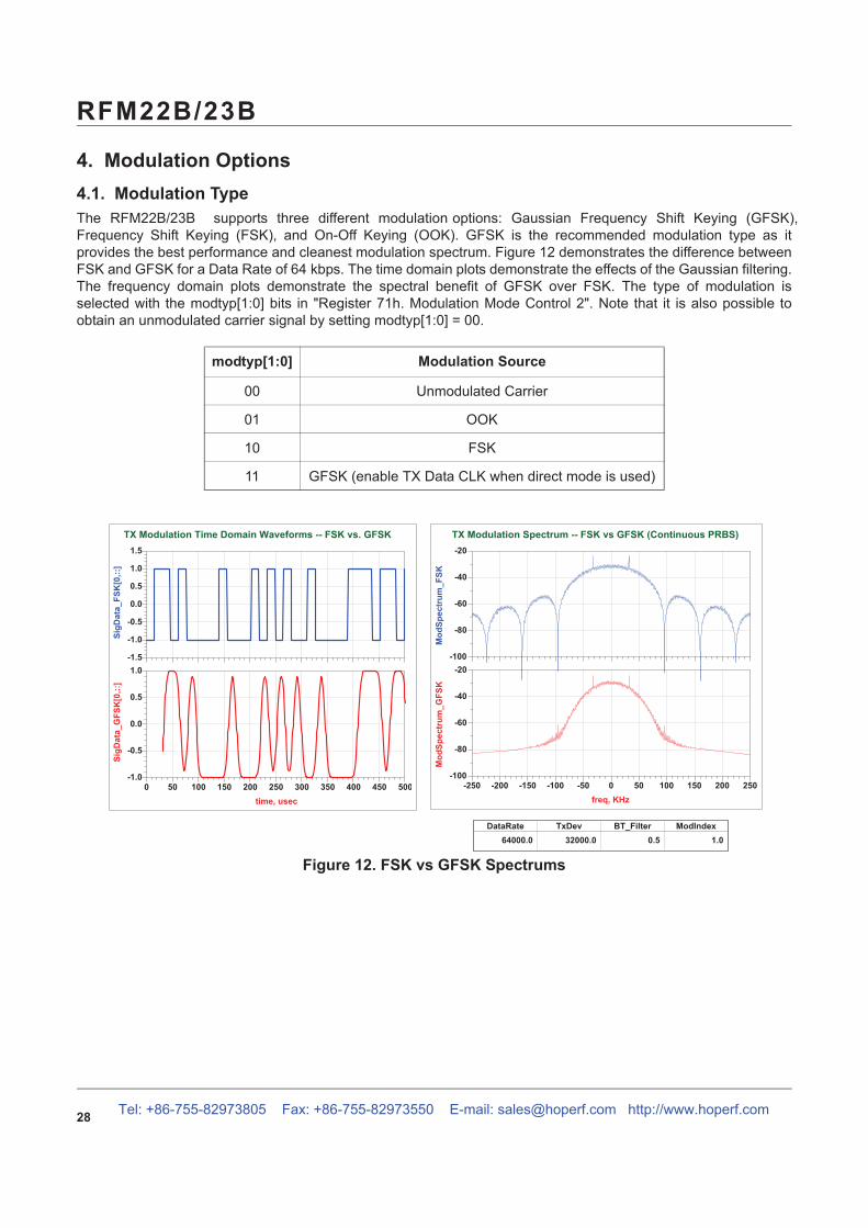
The RFM22B/23B supports three different modulation options: Gaussian Frequency Shift Keying (GFSK),
Frequency Shift Keying (FSK), and On-Off Keying (OOK). GFSK is the recommended modulation type as it
provides the best performance and cleanest modulation spectrum. Figure 12 demonstrates the difference between
FSK and GFSK for a Data Rate of 64 kbps. The time domain plots demonstrate the effects of the Gaussian filtering.
The frequency domain plots demonstrate the spectral benefit of GFSK over FSK. The type of modulation is
selected with the modtyp[1:0] bits in "Register 71h. Modulation Mode Control 2". Note that it is also possible to
obtain an unmodulated carrier signal by setting modtyp[1:0] = 00.
00 Unmodulated Carrier
01 OOK
10 FSK
11 GFSK (enable TX Data CLK when direct mode is used)
TX Modulation Time Domain Waveforms -- FSK vs. GFSK
-1.0
-0.5
0.0
0.5
1.0
-1.5
1.5
SigData_FSK[0,::]
50 100 150 200 250 300 350 400 4500 500
-0.5
0.0
0.5
-1.0
1.0
time, usec
SigData_GFSK[0,::]
TX Modulation Spectrum -- FSK vs GFSK (Continuous PRBS)
-80
-60
-40
-100
-20
ModSpectrum_FSK
-200 -150 -100 -50 0 50 100 150 200-250 250
-80
-60
-40
-100
-20
freq, KHz
ModSpectrum_GFSK
DataRate
64000.0
TxDev
32000.0
BT_Filter
0.5
ModIndex
1.0
Tel: +86-755-82973805 Fax: +86-755-82973550 E-mail: [email protected] http://www.hoperf.com

The RFM22B/23B may be configured to obtain its modulation data from one of three different sources: FIFO mode,
Direct Mode, and from a PN9 mode. In Direct Mode, the TX modulation data may be obtained from several
different input pins. These options are set through the dtmod[1:0] field in "Register 71h. Modulation Mode Control
2".
In FIFO mode, the transmit and receive data is stored in integrated FIFO register memory. The FIFOs are
accessed via "Register 7Fh. FIFO Access," and are most efficiently accessed with burst read/write operation as
discussed in "3.1. Serial Peripheral Interface (SPI)" .
In TX mode, the data bytes stored in FIFO memory are "packaged" together with other fields and bytes of
information to construct the final transmit packet structure. These other potential fields include the Preamble, Sync
word, Header, CRC checksum, etc. The configuration of the packet structure in TX mode is determined by the
Automatic Packet Handler (if enabled), in conjunction with a variety of Packet Handler Registers (see Table 13).
If the Automatic Packet Handler is disabled, the entire desired packet structure should be loaded intoFIFO memory; no other fields (such as Preamble or Sync word are automatically added to the bytes stored in FIFO
memory). For further information on the configuration of the FIFOs for a specific application or packet size, see "6.
Data Handling and Packet Handler" .
In RX mode, only the bytes of the received packet structure that are considered to be "data bytes" are stored in
FIFO memory. Which bytes of the received packet are considered "data bytes" is determined by the Automatic
Packet Handler (if enabled), in conjunction with the Packet Handler Registers (see Table 13 ). If the
Automatic Packet Handler is disabled, all bytes following the Sync word are considered data bytes and are stored
in FIFO memory. Thus, even if Automatic Packet Handling operation is not desired, the preamble detection
threshold and Sync word still need to be programmed so that the RX Modem knows when to start filling data into
the FIFO. When the FIFO is being used in RX mode, all of the received data may still be observed directly (in real-
time) by properly programming a GPIO pin as the RXDATA output pin; this can be quite useful during application
development.
When in FIFO mode, the chip will automatically exit the TX or RX State when either the ipksent or ipkvalid interrupt
occurs. The chip will return to the IDLE mode state programmed in "Register 07h. Operating Mode and Function
Control 1". For example, the chip may be placed into TX mode by setting the txon bit, but with the pllon bit
additionally set. The chip will transmit all of the contents of the FIFO and the ipksent interrupt will occur. When this
interrupt event occurs, the chip will clear the txon bit and return to TUNE mode, as indicated by the set state of the
pllon bit. If no other bits are additionally set in register 07h (besides txon initially), then the chip will return to the
STANDBY state.
In RX mode, the rxon bit will be cleared if ipkvalid occurs and the rxmpk bit (RX Multi-Packet bit, SPI Register 08h
bit [4]) is not set. When the rxmpk bit is set, the part will not exit the RX state after successfully receiving a packet,
but will remain in RX mode. The microcontroller will need to decide on the appropriate subsequent action,
depending upon information such as an interrupt generated by CRC, packet valid, or preamble detect.
71 R/W Modulation Mode
Control 2
trclk[1] trclk[0] dtmod[1] dtmod[0] eninv fd[8] modtyp[1] modtyp[0] 00h
00 Direct Mode using TX/RX Data via GPIO pin (GPIO configuration required)
01 Direct Mode using TX/RX Data via SDI pin (only when nSEL is high)
10 FIFO Mode
11 PN9 (internally generated)
Tel: +86-755-82973805 Fax: +86-755-82973550 E-mail: [email protected] http://www.hoperf.com

For legacy systems that perform packet handling within an MCU or other baseband chip, it may not be desirable to
use the FIFO. For this scenario, a Direct Mode is provided which bypasses the FIFOs entirely.
In TX direct mode, the TX modulation data is applied to an input pin of the chip and processed in "real time" (i.e.,
not stored in a register for transmission at a later time). A variety of pins may be configured for use as the TX Data
input function.
Furthermore, an additional pin may be required for a TX Clock output function if GFSK modulation is desired (only
the TX Data input pin is required for FSK). Two options for the source of the TX Data are available in the dtmod[1:0]
field, and various configurations for the source of the TX Data Clock may be selected through the trclk[1:0] field.
The eninv bit in SPI Register 71h will invert the TX Data; this is most likely useful for diagnostic and testing
purposes.
In RX direct mode, the RX Data and RX Clock can be programmed for direct (real-time) output to GPIO pins. The
microcontroller may then process the RX data without using the FIFO or packet handler functions of the RFIC. In
RX direct mode, the chip must still acquire bit timing during the Preamble, and thus the preamble detection
threshold (SPI Register 35h) must still be programmed. Once the preamble is detected, certain bit timing functions
within the RX Modem change their operation for optimized performance over the remainder of the packet. It is not
required that a Sync word be present in the packet in RX Direct mode; however, if the Sync word is absent then the
skipsyn bit in SPI Register 33h must be set, or else the bit timing and tracking function within the RX Modem will
not be configured for optimum performance.
In TX direct mode, the chip may be configured for synchronous or asynchronous modes of modulation. In direct
synchronous mode, the RFIC is configured to provide a TX Clock signal as an output to the external device that is
providing the TX Data stream. This TX Clock signal is a square wave with a frequency equal to the programmed
data rate. The external modulation source (e.g., MCU) must accept this TX Clock signal as an input and respond
by providing one bit of TX Data back to the RFIC, synchronous with one edge of the TX Clock signal. In this
fashion, the rate of the TX Data input stream from the external source is controlled by the programmed data rate of
the RFIC; no TX Data bits are made available at the input of the RFIC until requested by another cycle of the TX
Clock signal. The TX Data bits supplied by the external source are transmitted directly in real-time (i.e., not stored
internally for later transmission).
All modulation types (FSK/GFSK/OOK) are valid in TX direct synchronous mode. As will be discussed in the next
section, there are limits on modulation types in TX direct asynchronous mode.
In TX direct asynchronous mode, the RFIC no longer controls the data rate of the TX Data input stream. Instead,
the data rate is controlled only by the external TX Data source; the RFIC simply accepts the data applied to its TX
Data input pin, at whatever rate it is supplied. This means that there is no longer a need for a TX Clock output
signal from the RFIC, as there is no synchronous "handshaking" between the RFIC and the external data source.
The TX Data bits supplied by the external source are transmitted directly in real-time (i.e., not stored internally for
later transmission).
It is not necessary to program the data rate parameter when operating in TX direct asynchronous mode. The chip
still internally samples the incoming TX Data stream to determine when edge transitions occur; however, rather
than sampling the data at a pre-programmed data rate, the chip now internally samples the incoming TX Data
stream at its maximum possible oversampling rate. This allows the chip to accurately determine the timing of the bit
edge transitions without prior knowledge of the data rate. (Of course, it is still necessary to program the desired
peak frequency deviation.)
00 No TX Clock (only for FSK)
01 TX/RX Data Clock is available via GPIO (GPIO needs programming accordingly as well)
10 TX/RX Data Clock is available via SDO pin (only when nSEL is high)
11 TX/RX Data Clock is available via the nIRQ pin
Tel: +86-755-82973805 Fax: +86-755-82973550 E-mail: [email protected] http://www.hoperf.com

Only FSK and OOK modulation types are valid in TX Direct Asynchronous Mode; GFSK modulation is not available
in asynchronous mode. This is because the RFIC does not have knowledge of the supplied data rate, and thus
cannot determine the appropriate Gaussian lowpass filter function to apply to the incoming data.
One advantage of this mode that it saves a microcontroller pin because no TX Clock output function is required.
The primary disadvantage of this mode is the increase in occupied spectral bandwidth with FSK (as compared to
GFSK).
In certain applications it may be desirable to minimize the connections to the microcontroller or to preserve the
GPIOs for other uses. For these cases it is possible to use the SPI pins and nIRQ as the modulation clock and
data. The SDO pin can be configured to be the data clock by programming trclk = 10. If the nSEL pin is LOW then
the function of the pin will be SPI data output. If the pin is high and trclk[1:0] is 10 then during RX and TX modes
the data clock will be available on the SDO pin. If trclk[1:0] is set to 11 and no interrupts are enabled in registers 05
or 06h, then the nIRQ pin can also be used as the TX/RX data clock.
The SDI pin can be configured to be the data source in both RX and TX modes if dtmod[1:0] = 01. In a similar
fashion, if nSEL is LOW the pin will function as SPI data-in. If nSEL is HIGH then in TX mode it will be the data to
C
DATACLK
MOD
nRES
MOSI
MISO
SCK
nSEL
nIRQ
Direct synchronous modulation. Full
control over the standard SPI & using
interrupt. Bitrate clock and modulation
via GPIO’s.
GPIO configuration
GP0 : power-on-reset (default)
GP1 : TX DATA clock output
GP2 : TX DATA input
DataCLK
MOD(Data)
VDD_RF
TX
RXp
RXn
SCLK
SDI
SDO
VDD_DIG
AN
T1
GP
IO_0
GP
IO_
1
GP
IO_2
XIN
XO
UT
SD
N
nIR
Q
NC NC
VR
_D
IGn
SE
L
Matching
C
MOD
nRES
MOSI
MISO
SCK
nSEL
nIRQ
Direct asynchronous FSK modulation.
Modulation data via GPIO2, no data
clock needed in this mode.
GPIO configuration
GP0 : power-on-reset (default)
GP1: not utilized
GP2 : TX DATA input
MOD(Data)
VDD_RF
TX
RXp
RXn
SCLK
SDI
SDO
VDD_DIG
AN
T1
GP
IO_
0
GP
IO_1
GP
IO_2
XIN
XO
UT
SD
N
nIR
Q
NC NC
VR
_D
IGn
SE
L
Matching
Tel: +86-755-82973805 Fax: +86-755-82973550 E-mail: [email protected] http://www.hoperf.com

be modulated and transmitted. In RX mode it will be the received demodulated data. Figure 15 demonstrates using
SDI and SDO as the TX/RX data and clock:
If the SDO pin is not used for data clock then it may be programmed to be the interrupt function (nIRQ) by
programming Reg 0Eh bit 3.
In this mode the TX Data is generated internally using a pseudorandom (PN9 sequence) bit generator. The primary
purpose of this mode is for use as a test mode to observe the modulated spectrum without having to provide data.
SPI input don’t care SPI input
TX on
commandTX mode
MOD input
TX off
command
SPI input don’t care
RX on
commandRX mode
RX off
command
Data outputSPI input SPI input
SPI output SPI output SPI output SPI output SPI outputdon’t care don’t careData CLK
OutputData CLK
Output
Tel: +86-755-82973805 Fax: +86-755-82973550 E-mail: [email protected] http://www.hoperf.com
This section provides an overview some of the key blocks of the internal radio architecture.
The LNA provides gain with a noise figure low enough to suppress the noise of t he following stages.
which is controlled by the analog gain control (AGC) algo The AGC algorithm adjusts the gain of the LNA and PGA so the receiver can handle signal levels from
For the RFM23B, The direct tie is used, The lna_sw bit in “Register 6Dh. TX Power” must be set.
The output of the LNA is fed internally to the input of the receive mixer. The receive mixer is implemented as an I-Q
mixer that provides both I and Q channel outputs to the programmable gain amplifier. The mixer consists of two
double-balanced mixers whose RF inputs are driven in parallel, local oscillator (LO) inputs are driven in quadrature,
and separate I and Q Intermediate Frequency (IF) outputs drive the programmable gain amplifier. The receive LO
signal is supplied by an integrated VCO and PLL synthesizer operating between 240–960 MHz. The necessary
quadrature LO signals are derived from the divider at the VCO output.
The programmable gain amplifier (PGA) provides the necessary gain to boost the signal level into the dynamic
range of the ADC. The PGA must also have enough gain switching to allow for large input signals to ensure a
linear RSSI range up to –20 dBm. The PGA has steps of 3 dB which are controlled by the AGC algorithm in the
digital modem.
The amplified IQ IF signals are digitized using an Analog-to-Digital Converter (ADC), which allows for low current
consumption and high dynamic range. The bandpass response of the ADC provides exceptional rejection of out of
band blockers.
Using high-performance ADCs allows channel filtering, image rejection, and demodulation to be performed in the
digital domain, resulting in reduced area while increasing flexibility. The digital modem performs the following
functions:
Channel selection filter
TX modulation
RX demodulation
AGC
Preamble detector
Invalid preamble detector
Radio signal strength indicator (RSSI)
Automatic frequency compensation (AFC)
Packet handling including EZMAC® features
Cyclic redundancy check (CRC)
The digital channel filter and demodulator are optimized for ultra low power consumption and are highly
configurable. Supported modulation types are GFSK, FSK, and OOK. The channel filter can be configured to
support bandwidths ranging from 620 kHz down to 2.6 kHz. A large variety of data rates are supported ranging
from 0.123 up to 256 kbps. The AGC algorithm is implemented digitally using an advanced control loop optimized
for fast response time.
Tel: +86-755-82973805 Fax: +86-755-82973550 E-mail: [email protected] http://www.hoperf.com
The LNA has one step of gain control rithm.
om sensitivity to +5 dBm with optimal performance.

The configurable preamble detector is used to improve the reliability of the sync-word detection. The sync-word
detector is only enabled when a valid preamble is detected, significantly reducing the probability of false detection.
The received signal strength indicator (RSSI) provides a measure of the signal strength received on the tuned
channel. The resolution of the RSSI is 0.5 dB. This high resolution RSSI enables accurate channel power
measurements for clear channel assessment (CCA), carrier sense (CS), and listen before talk (LBT) functionality.
Frequency mistuning caused by crystal inaccuracies can be compensated by enabling the digital automatic
frequency control (AFC) in receive mode.
A comprehensive programmable packet handler including key features of HOPERF’ EZMAC is integrated to
create a variety of communication topologies ranging from peer-to-peer networks to mesh networks. The extensive
programmability of the packet header allows for advanced packet filtering which in turn enables a mix of broadcast,
group, and point-to-point communication.
A wireless communication channel can be corrupted by noise and interference, and it is therefore important to
know if the received data is free of errors. A cyclic redundancy check (CRC) is used to detect the presence of
erroneous bits in each packet. A CRC is computed and appended at the end of each transmitted packet and
verified by the receiver to confirm that no errors have occurred. The packet handler and CRC can significantly
reduce the load on the system microcontroller allowing for a simpler and cheaper microcontroller.
The digital modem includes the TX modulator which converts the TX data bits into the corresponding stream of
digital modulation values to be summed with the fractional input to the sigma-delta modulator. This modulation
approach results in highly accurate resolution of the frequency deviation. A Gaussian filter is implemented to
support GFSK, considerably reducing the energy in the adjacent channels. The default bandwidth-time product
(BT) is 0.5 for all programmed data rates, but it may not be adjusted to other values.
An integrated Sigma Delta ( ) Fractional-N PLL synthesizer capable of operating from 240–960 MHz is provided
Using a synthesizer has many advantages; it provides flexibility in
frequency, and channel spacing. The transmit modulation is applied directly to the loop in the digital domain
through the fractional divider which results in very precise accuracy and control over the transmit deviation.
Depending on the part, the PLL and - modulator scheme is designed to support any desired frequency and
channel spacing in the range from 240–960 MHz with a frequency resolution of 156.25 Hz (Low band) or 312.5 Hz
(High band). The transmit data rate can be programmed between 0.123–256 kbps, and the frequency deviation
can be programmed between ±1–320 kHz. These parameters may be adjusted via registers as shown in "3.5.
Frequency Control".
The reference frequency to the PLL is 10 MHz. The PLL utilizes a differential L-C VCO, with integrated on-chip
inductors. The output of the VCO is followed by a configurable divider which will divide down the signal to the
desired output frequency band. The modulus of the variable divide-by-N divider stage is controlled dynamically by
Tel: +86-755-82973805 Fax: +86-755-82973550 E-mail: [email protected] http://www.hoperf.com
choosing data rate, deviation, channel
the output from the - modulator. The tuning resolution is sufficient to tune to the commanded frequency with a
maximum accuracy of 312.5 Hz anywhere in the range between 240–960 MHz.
The output of the VCO is automatically divided down to the correct output frequency depending on the hbsel and
fb[4:0] fields in "Register 75h. Frequency Band Select." In receive mode, the LO frequency is automatically shifted
downwards by the IF frequency of 937.5 kHz, allowing transmit and receive operation on the same frequency. The
VCO integrates the resonator inductor and tuning varactor, so no external VCO components are required.
The VCO uses a capacitance bank to cover the wide frequency range specified. The capacitance bank will
automatically be calibrated every time the synthesizer is enabled. In certain fast hopping applications this might not
be desirable so the VCO calibration may be skipped by setting the appropriate register.
The RFM22B contains an internal integrated power amplifier (PA) capable of transmitting at output levels between –1
and +20 dBm. The RFM23B contains a PA which is capable of transmitting output levels between –8 to
+13 dBm. The PA design is single-ended and is implemented as a two stage class CE amplifier with a high
efficiency when transmitting at maximum power. The PA efficiency can only be optimized at one power level.
Changing the output power by adjusting txpow[2:0] will scale both the output power and current but the efficiency
will not remain constant. The PA output is ramped up and down to prevent unwanted spectral splatter.
For the RFM23B,
.
The direct tie is used, The lna_sw bit in “Register 6Dh. TX Power” must be set.
The output power is configurable in 3 dB steps with the txpow[2:0] field in "Register 6Dh. TX Power." Extra output
power can allow the use of a cheaper smaller antenna, greatly reducing the overall BOM cost. The higher power
setting of the chip achieves maximum possible range, but of course comes at the cost of higher TX current
consumption. However, depending on the duty cycle of the system, the effect on battery life may be insignificant.
Contact HOPERF Support for help in evaluating this tradeoff.
6D R/W TX Power papeakval papeaken papeaklv[1] papeaklv[0] lna_sw txpow[2] txpow[1] txpow[0] 18h
000 +1 dBm
001 +2 dBm
010 +5 dBm
011 +8 dBm
100 +11 dBm
101 +14 dBm
110 +17 dBm
111 +20 dBm
000 –8 dBm
001 –5 dBm
010 –2 dBm
011 +1 dBm
100 +4 dBm
101 +7 dBm
110 +10 dBm
111 +13 dBm
Tel: +86-755-82973805 Fax: +86-755-82973550 E-mail: [email protected] http://www.hoperf.com

The RFM22B/23B includes an integrated 30 MHz crystal oscillator with a fast start-up time of less than 600 s.
A parallel resonant 30MHz crystal is used on the module. The design is differential with the required capacitance integrated on-chip to minimize the number of external components.
The crystal load capacitance can be digitally programmed to accommodate crystals with various load capacitance
requirements and to adjust the frequency of the crystal oscillator. The tuning of the crystal load capacitance is
programmed through the xlc[6:0] field of "Register 09h. 30 MHz Crystal Oscillator Load Capacitance." The total
internal capacitance is 12.5 pF and is adjustable in approximately 127 steps (97fF/step). The xtalshift bit provides a
coarse shift in frequency but is not binary with xlc[6:0].
The crystal frequency adjustment can be used to compensate for crystal production tolerances. Utilizing the on-
chip temperature sensor and suitable control software, the temperature dependency of the crystal can be
canceled.
The typical value of the total on-chip capacitance Cint can be calculated as follows:
Cint = 1.8 pF + 0.085 pF x xlc[6:0] + 3.7 pF x xtalshift
Note that the coarse shift bit xtalshift is not binary with xlc[6:0]. The total load capacitance Cload seen by the crystal
can be calculated by adding the sum of all external parasitic PCB capacitances Cext to Cint. If the maximum value
of Cint (16.3 pF) is not sufficient, an external capacitor can be added for exact tuning.
If AFC is disabled then the synthesizer frequency may be further adjusted by programming the Frequency Offset
field fo[9:0]in "Register 73h. Frequency Offset 1" and "Register 74h. Frequency Offset 2", as discussed in "3.5.
Frequency Control" .
The crystal oscillator frequency is divided down internally and may be output to the microcontroller through one of
the GPIO pins for use as the System Clock. In this fashion, only one crystal oscillator is required for the entire
system and the BOM cost is reduced. The available clock frequencies and GPIO configuration are discussed
further in "8.2. Microcontroller Clock" .
There are a total of six regulators integrated onto the RF M22B/23B . With the exception of the digital regulator, all
regulators are designed to operate with only internal decoupling.
input supply voltage from +1.8 to +3.6V. A supply voltage should only be connected to the VDD pins.
09 R/W Crystal Oscillator Load
Capacitance
xtalshift xlc[6] xlc[5] xlc[4] xlc[3] xlc[2] xlc[1] xlc[0] 7Fh
Tel: +86-755-82973805 Fax: +86-755-82973550 E-mail: [email protected] http://www.hoperf.com
crystal load
All regulators are designed to operate with an

The internal modem is designed to operate with a packet including a 10101... preamble structure. To configure the
modem to operate with packet formats without a preamble or other legacy packet structures contact customer
support.
Two 64 byte FIFOs are integrated into the chip, one for RX and one for TX, as shown in Figure 17. "Register 7Fh.
FIFO Access" is used to access both FIFOs. A burst write, as described in "3.1. Serial Peripheral Interface (SPI)"
to address 7Fh will write da ta to the TX FIFO. A burst read from address 7Fh will read data from the RX FIFO.
The TX FIFO has two programmable thresholds. An interrupt event occurs when the data in the TX FIFO reaches
these thresholds. The first threshold is the FIFO almost full threshold, txafthr[5:0]. The value in this register
corresponds to the desired threshold value in number of bytes. When the data being filled into the TX FIFO crosses
this threshold limit, an interrupt to the microcontroller is generated so the chip can enter TX mode to transmit the
contents of the TX FIFO. The second threshold for TX is the FIFO almost empty threshold, txaethr[5:0]. When the
data being shifted out of the TX FIFO drops below the almost empty threshold an interrupt will be generated. The
microcontroller will need to switch out of TX mode or fill more data into the TX FIFO. The transceiver can be
configured so that when the TX FIFO is empty it will automatically exit the TX state and return to one of the low
power states. When TX is initiated, it will transmit the number of bytes programmed into the packet length field
(Reg 3Eh). When the packet ends, the chip will return to the state specified in register 07h. For example, if 08h is
written to address 07h then the chip will return to the STANDBY state. If 09h is written then the chip will return to
the READY state.
RX FIFO Almost Full
Threshold
TX FIFO Almost Empty
Threshold
TX FIFO Almost Full
Threshold
Tel: +86-755-82973805 Fax: +86-755-82973550 E-mail: [email protected] http://www.hoperf.com

The RX FIFO has one programmable threshold called the FIFO Almost Full Threshold, rxafthr[5:0]. When the
incoming RX data crosses the Almost Full Threshold an interrupt will be generated to the microcontroller via the
nIRQ pin. The microcontroller will then need to read the data from the RX FIFO.
Both the TX and RX FIFOs may be cleared or reset with the ffclrtx and ffclrrx bits. All interrupts may be enabled by
setting the Interrupt Enabled bits in "Register 05h. Interrupt Enable 1" and “Register 06h. Interrupt Enable 2.” If the
interrupts are not enabled the function will not generate an interrupt on the nIRQ pin but the bits will still be read
correctly in the Interrupt Status registers.
When using the FIFOs, automatic packet handling may be enabled for TX mode, RX mode, or both. "Register 30h.
Data Access Control" through “Register 4Bh. Received Packet Length” control the configuration, status, and
decoded RX packet data for Packet Handling. The usual fields for network communication (such as preamble,
synchronization word, headers, packet length, and CRC) can be configured to be automatically added to the data
payload. The fields needed for packet generation normally change infrequently and can therefore be stored in
registers. Automatically adding these fields to the data payload greatly reduces the amount of communication
between the microcontroller and the RFM22B/23B and reduces the required computational power of the
microcontroller.
The general packet structure is shown in Figure 18. The length of each field is shown below the field. The preamble
pattern is always a series of alternating ones and zeroes, starting with a zero. All the fields have programmable
lengths to accommodate different applications. The most common CRC polynominals are available for selection.
An overview of the packet handler configuration registers is shown in Table 13.
08 R/W Operating &
Function
Control 2
antdiv[2] antdiv[1] antdiv[0] rxmpk autotx enldm ffclrrx ffclrtx 00h
7C R/W TX FIFO
Control 1
Reserved Reserved txafthr[5] txafthr[4] txafthr[3] txafthr[2] txafthr[1] txafthr[0] 37h
7D R/W TX FIFO
Control 2
Reserved Reserved txaethr[5] txaethr[4] txaethr[3] txaethr[2] txaethr[1] txaethr[0] 04h
7E R/W RX FIFO
Control
Reserved Reserved rxafthr[5] rxafthr[4] rxafthr[3] rxafthr[2] rxafthr[1] rxafthr[0] 37h
Tel: +86-755-82973805 Fax: +86-755-82973550 E-mail: [email protected] http://www.hoperf.com

If the TX packet length is set the packet handler will send the number of bytes in the packet length field before
returning to IDLE mode and asserting the packet sent interrupt. To resume sending data from the FIFO the
microcontroller needs to command the chip to re-enter TX mode. Figure 19 provides an example transaction where
the packet length is set to three bytes.
When the packet handler is disabled certain fields in the received packet are still required. Proper modem
operation requires preamble and sync when the FIFO is being used, as shown in Figure 20. Bits after sync will be
treated as raw data with no qualification. This mode allows for the creation of a custom packet handler when the
automatic qualification parameters are not sufficient. Manchester encoding is supported but data whitening, CRC,
and header checks are not.
When the packet handler is enabled, all the fields of the packet structure need to be configured. Register contents
are used to construct the header field and length information encoded into the transmitted packet when
transmitting. The receive FIFO can be configured to handle packets of fixed or variable length with or without a
header. If multiple packets are desired to be stored in the FIFO, then there are options available for the different
fields that will be stored into the FIFO. Figure 21 demonstrates the options and settings available when multiple
packets are enabled. Figure 22 demonstrates the operation of fixed packet length and correct/incorrect packets.
Data 1
Data 2
Data 3
Data 4
Data 5
Data 6
Data 7
Data 8
Data 9
}
}
}
This will be sent in the first transm ission
This will be sent in the second transmission
This will be sent in the third transm ission
Register
Data
RegisterData
Data
eader(s)
ength
rx_multi_pk_en = 1
H
Data
rx_multi_pk_en = 0
txhdlen = 0 txhdlen > 0
fixpklenfixpklen
Data DataData Data
L L
H
Tel: +86-755-82973805 Fax: +86-755-82973550 E-mail: [email protected] http://www.hoperf.com

Data
L
H
Data
L
H
Data
LH
Data
L
H
Data
L
H
Data
LH
Data
L
H
Data
LH
Data
L
H
Tel: +86-755-82973805 Fax: +86-755-82973550 E-mail: [email protected] http://www.hoperf.com

30 R/W Data Access Control enpacrx lsbfrst crcdonly skip2ph enpactx encrc crc[1] crc[0] 8Dh
31 R EzMAC status 0 rxcrc1 pksrch pkrx pkvalid crcerror pktx pksent —
32 R/W Header Control 1 bcen[3:0] hdch[3:0] 0Ch
33 R/W Header Control 2 skipsyn hdlen[2] hdlen[1] hdlen[0] fixpklen synclen[1] synclen[0] prealen[8] 22h
34 R/W Preamble Length prealen[7] prealen[6] prealen[5] prealen[4] prealen[3] prealen[2] prealen[1] prealen[0] 08h
35 R/W Preamble Detection Control preath[4] preath[3] preath[2] preath[1] preath[0] rssi_off[2] rssi_off[1] rssi_off[0] 2Ah
36 R/W Sync Word 3 sync[31] sync[30] sync[29] sync[28] sync[27] sync[26] sync[25] sync[24] 2Dh
37 R/W Sync Word 2 sync[23] sync[22] sync[21] sync[20] sync[19] sync[18] sync[17] sync[16] D4h
38 R/W Sync Word 1 sync[15] sync[14] sync[13] sync[12] sync[11] sync[10] sync[9] sync[8] 00h
39 R/W Sync Word 0 sync[7] sync[6] sync[5] sync[4] sync[3] sync[2] sync[1] sync[0] 00h
3A R/W Transmit Header 3 txhd[31] txhd[30] txhd[29] txhd[28] txhd[27] txhd[26] txhd[25] txhd[24] 00h
3B R/W Transmit Header 2 txhd[23] txhd[22] txhd[21] txhd[20] txhd[19] txhd[18] txhd[17] txhd[16] 00h
3C R/W Transmit Header 1 txhd[15] txhd[14] txhd[13] txhd[12] txhd[11] txhd[10] txhd[9] txhd[8] 00h
3D R/W Transmit Header 0 txhd[7] txhd[6] txhd[5] txhd[4] txhd[3] txhd[2] txhd[1] txhd[0] 00h
3E R/W Transmit Packet Length pklen[7] pklen[6] pklen[5] pklen[4] pklen[3] pklen[2] pklen[1] pklen[0] 00h
3F R/W Check Header 3 chhd[31] chhd[30] chhd[29] chhd[28] chhd[27] chhd[26] chhd[25] chhd[24] 00h
40 R/W Check Header 2 chhd[23] chhd[22] chhd[21] chhd[20] chhd[19] chhd[18] chhd[17] chhd[16] 00h
41 R/W Check Header 1 chhd[15] chhd[14] chhd[13] chhd[12] chhd[11] chhd[10] chhd[9] chhd[8] 00h
42 R/W Check Header 0 chhd[7] chhd[6] chhd[5] chhd[4] chhd[3] chhd[2] chhd[1] chhd[0] 00h
43 R/W Header Enable 3 hden[31] hden[30] hden[29] hden[28] hden[27] hden[26] hden[25] hden[24] FFh
44 R/W Header Enable 2 hden[23] hden[22] hden[21] hden[20] hden[19] hden[18] hden[17] hden[16] FFh
45 R/W Header Enable 1 hden[15] hden[14] hden[13] hden[12] hden[11] hden[10] hden[9] hden[8] FFh
46 R/W Header Enable 0 hden[7] hden[6] hden[5] hden[4] hden[3] hden[2] hden[1] hden[0] FFh
47 R Received Header 3 rxhd[31] rxhd[30] rxhd[29] rxhd[28] rxhd[27] rxhd[26] rxhd[25] rxhd[24] —
48 R Received Header 2 rxhd[23] rxhd[22] rxhd[21] rxhd[20] rxhd[19] rxhd[18] rxhd[17] rxhd[16] —
49 R Received Header 1 rxhd[15] rxhd[14] rxhd[13] rxhd[12] rxhd[11] rxhd[10] rxhd[9] rxhd[8] —
4A R Received Header 0 rxhd[7] rxhd[6] rxhd[5] rxhd[4] rxhd[3] rxhd[2] rxhd[1] rxhd[0] —
4B R Received Packet Length rxplen[7] rxplen[6] rxplen[5] rxplen[4] rxplen[3] rxplen[2] rxplen[1] rxplen[0] —
Tel: +86-755-82973805 Fax: +86-755-82973550 E-mail: [email protected] http://www.hoperf.com

Data whitening can be used to avoid extended sequences of 0s or 1s in the transmitted data stream to achieve a
more uniform spectrum. When enabled, the payload data bits are XORed with a pseudorandom sequence output
from the built-in PN9 generator. The generator is initialized at the beginning of the payload. The receiver recovers
the original data by repeating this operation. Manchester encoding can be used to ensure a dc-free transmission
and good synchronization properties. When Manchester encoding is used, the effective datarate is unchanged but
the actual datarate (preamble length, etc.) is doubled due to the nature of the encoding. The effective datarate
when using Manchester encoding is limited to 128 kbps. The implementation of Manchester encoding is shown in
Figure 24. Data whitening and Manchester encoding can be selected with "Register 70h. Modulation Mode Control
1". The CRC is configured via "Register 30h. Data Access Control." Figure 23 demonstrates the portions of the
packet which have Manchester encoding, data whitening, and CRC applied. CRC can be applied to only the data
portion of the packet or to the data, packet length and header fields. Figure 24 provides an example of how the
Manchester encoding is done and also the use of the Manchester invert (enmaniv) function.
The RFM22B/23B has integrated automatic preamble detection. The preamble length is configurable from 1–256bytes using the prealen[7:0] field in "Register 33h. Header Control 2" and "Register 34h. Preamble Length", asdescribed in “6.2. Packet Configuration”. The preamble detection threshold, preath[4:0] as set in "Register 35h.Preamble Detection Control 1", is in units of 4 bits. The preamble detector searches for a preamble pattern with alength of preath[4:0].
If a false preamble detect occurs, the receiver will continuing searching for the preamble when no sync word isdetected. Once preamble is detected (false or real) then the part will then start searching for sync. If no sync occursthen a timeout will occur and the device will initiate search for preamble again. The timeout period is defined as thesync word length plus four bits and will start after a non-preamble pattern is recognized after a valid preambledetection. The preamble detector output may be programmed onto one of the GPIO or read in the interrupt statusregisters.
1 1 11 1 1 1 1 00 0 0 1
0 0 00 0 0 0 0
Preamble = 0xFF First 4bits of the synch. word = 0x2
Preamble = 0x00 First 4bits of the synch. word = 0x2
0 0 0 10
Tel: +86-755-82973805 Fax: +86-755-82973550 E-mail: [email protected] http://www.hoperf.com

The preamble detection threshold determines the number of valid preamble bits the radio must receive to qualify a
valid preamble. The preamble threshold should be adjusted depending on the nature of the application. The
required preamble length threshold will depend on when receive mode is entered in relation to the start of the
transmitted packet and the length of the transmit preamble. With a shorter than recommended preamble detection
threshold the probability of false detection is directly related to how long the receiver operates on noise before the
transmit preamble is received. False detection on noise may cause the actual packet to be missed. The preamble
detection threshold is programmed in register 35h. For most applications with a preamble length longer than 32 bits
the default value of 20 is recommended for the preamble detection threshold. A shorter Preamble Detection
Threshold may be chosen if occasional false detections may be tolerated. When antenna diversity is enabled a 20-
bit preamble detection threshold is recommended. When the receiver is synchronously enabled just before the
start of the packet, a shorter preamble detection threshold may be used. Table 14 demonstrates the recommended
preamble detection threshold and preamble length for various modes.
It is possible to use RFM22B/23B in a raw mode without the requirement for a 101010 preamble. Contact customer
support for further details.
The recommended preamble length and preamble detection threshold listed above are to achieve 0% PER. They may
be shortened when occasional packet errors are tolerable.
When scanning channels in a frequency hopping system it is desirable to determine if a channel is valid in the
minimum amount of time. The preamble detector can output an invalid preamble detect signal. which can be used
to identify the channel as invalid. After a configurable time set in Register 60h[7:4], an invalid preamble detect
signal is asserted indicating an invalid channel. The period for evaluating the signal for invalid preamble is defined
as (inv_pre_th[3:0] x 4) x Bit Rate Period. The preamble detect and invalid preamble detect signals are available in
"Register 03h. Interrupt/Status 1" and “Register 04h. Interrupt/Status 2.”
The synchronization word length for both TX and RX can be configured in Reg 33h, synclen[1:0]. The expected or
transmitted sync word can be configured from 1 to 4 bytes as defined below:
synclen[1:0] = 00—Expected/Transmitted Synchronization Word (sync word) 3.
synclen[1:0] = 01—Expected/Transmitted Synchronization Word 3 first, followed by sync word 2.
synclen[1:0] = 10—Expected/Transmitted Synchronization Word 3 first, followed by sync word 2, followed by
sync word 1.
synclen[1:0] = 1—Send/Expect Synchronization Word 3 first, followed by sync word 2, followed by sync word 1,
followed by sync word 0.
The sync is transmitted or expected in the following sequence: sync 3 sync 2 sync 1 sync 0. The sync word
values can be programmed in Registers 36h–39h. After preamble detection, the part will search for sync for a fixed
(G)FSK AFC Disabled 1 byte 20 bits 32 bits
(G)FSK AFC Enabled 2 byte 28 bits 40 bits
(G)FSK AFC Disabled +Antenna
Diversity Enabled1 byte — 64 bits
(G)FSK AFC Enabled +Antenna
Diversity Enabled2 byte — 8 byte
OOK 2 byte 3 byte 4 byte
OOK + Antenna Diversity Enabled 8 byte — 8 byte
Tel: +86-755-82973805 Fax: +86-755-82973550 E-mail: [email protected] http://www.hoperf.com

period of time. If a sync is not recognized in this period, a timeout will occur, and the search for preamble will be re-
initiated. The timeout period after preamble detections is defined as the value programmed into the sync word
length plus four additional bits.
The header check is designed to support 1–4 bytes and broadcast headers. The header length needs to be set in
register 33h, hdlen[2:0]. The headers to be checked need to be set in register 32h, hdch[3:0]. For instance, there
can be four bytes of header in the packet structure but only one byte of the header is set to be checked (i.e.,
header 3). For the headers that are set to be checked, the expected value of the header should be programmed in
chhd[31:0] in Registers 3F–42. The individual bits within the selected bytes to be checked can be enabled or
disabled with the header enables, hden[31:0] in Registers 43–46. For example, if you want to check all bits in
header 3 then hden[31:24] should be set to FF but if only the last 4 bits are desired to be checked then it should be
set to 00001111 (0F). Broadcast headers can also be programmed by setting bcen[3:0] in Register 32h. For
broadcast header check the value may be either “FFh” or the value stored in the Check Header register. A logic
equivalent of the header check for Header 3 is shown in Figure 25. A similar logic check will be done for Header 2,
Header 1, and Header 0 if enabled.
The RFM22B/23B is capable of automatically retransmitting the last packet loaded in the TX FIFO. Automatic
retransmission is set by entering the TX state with the txon bit without reloading the TX FIFO. This feature is useful
for beacon transmission or when retransmission is required due to the absence of a valid acknowledgement. Only
packets that fit completely in the TX FIFO can be automatically retransmitted.
An automatic transmission function is available, allowing the radio to automatically start or stop a transmission
depending on the amount of data in the TX FIFO.
When autotx is set in “Register 08. Operating & Function Control 2", the transceiver will automatically enter the TX
state when the TX FIFO almost full threshold is exceeded. Packets will be transmitted according to the configured
packet length. To stop transmitting, clear the packet sent or TX FIFO almost empty interrupts must be cleared by
reading register.
header3_ok
Equivalence
comparison
Equivalence
comparison
Tel: +86-755-82973805 Fax: +86-755-82973550 E-mail: [email protected] http://www.hoperf.com

A Microsoft Excel (WDS) parameter calculator or Wireless Development Suite (WDS) calculator is provided to
determine the proper settings for the modem. The calculator can be found on www.hoperf.com or on the CD
provided with the demo kits. An application note is available to describe how to use the calculator and to provide
advanced descriptions of the modem settings and calculations.
The modem performs channel selection and demodulation in the digital domain. The channel filter bandwidth is
configurable from 2.6 to 620 kHz. The receiver data-rate, modulation index, and bandwidth are set via registers
1C–25h. The modulation index is equal to 2 times the peak deviation divided by the data rate (Rb).
When Manchester coding is disabled, the required channel filter bandwidth is calculated as BW = 2Fd + Rb where
Fd is the frequency deviation and Rb is the data rate.
Tel: +86-755-82973805 Fax: +86-755-82973550 E-mail: [email protected] http://www.hoperf.com
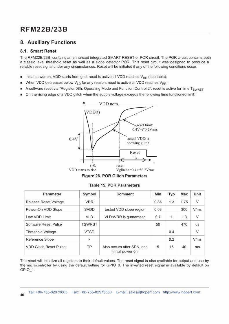
The RFM22B/23B contains an enhanced integrated SMART RESET or POR circuit. The POR circuit contains both
a classic level threshold reset as well as a slope detector POR. This reset circuit was designed to produce a
reliable reset signal under any circumstances. Reset will be initiated if any of the following conditions occur:
Initial power on, VDD starts from gnd: reset is active till VDD reaches VRR (see table);
When VDD decreases below VLD for any reason: reset is active till VDD reaches VRR;
A software reset via “Register 08h. Operating Mode and Function Control 2”: reset is active for time TSWRST
On the rising edge of a VDD glitch when the supply voltage exceeds the following time functioned limit:
The reset will initialize all registers to their default values. The reset signal is also available for output and use by
the microcontroller by using the default setting for GPIO_0. The inverted reset signal is available by default on
GPIO_1.
Release Reset Voltage VRR 0.85 1.3 1.75 V
Power-On VDD Slope SVDD tested VDD slope region 0.03 300 V/ms
Low VDD Limit VLD VLD<VRR is guaranteed 0.7 1 1.3 V
Software Reset Pulse TSWRST 50 470 us
Threshold Voltage VTSD 0.4 V
Reference Slope k 0.2 V/ms
VDD Glitch Reset Pulse TP Also occurs after SDN, and
initial power on
5 16 40 ms
Reset
TP
t=0,
VDD starts to rise
t
VDD(t)
reset:
Vglitch>=0.4+t*0.2V/ms
actual VDD(t)
showing glitch
reset limit:
0.4V+t*0.2V/ms
VDD nom.
0.4V
Tel: +86-755-82973805 Fax: +86-755-82973550 E-mail: [email protected] http://www.hoperf.com
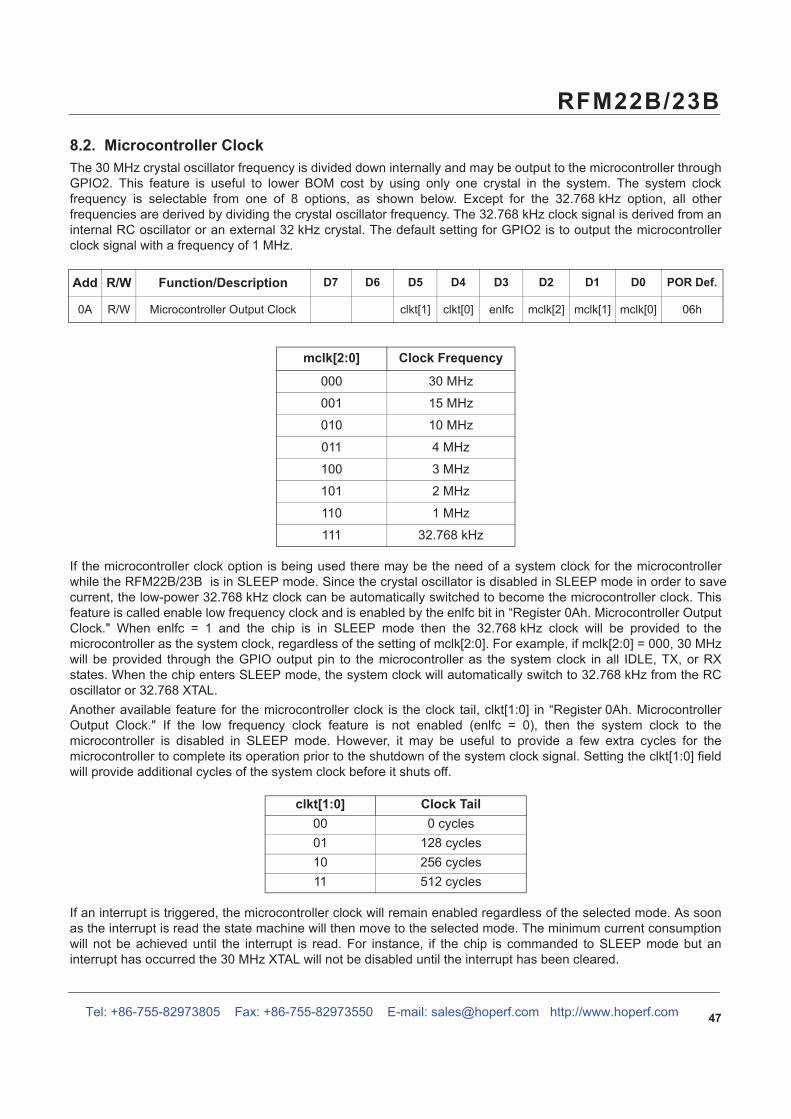
The 30 MHz crystal oscillator frequency is divided down internally and may be output to the microcontroller through
GPIO2. This feature is useful to lower BOM cost by using only one crystal in the system. The system clock
frequency is selectable from one of 8 options, as shown below. Except for the 32.768 kHz option, all other
frequencies are derived by dividing the crystal oscillator frequency. The 32.768 kHz clock signal is derived from an
internal RC oscillator or an external 32 kHz crystal. The default setting for GPIO2 is to output the microcontroller
clock signal with a frequency of 1 MHz.
If the microcontroller clock option is being used there may be the need of a system clock for the microcontroller
while the RFM22B/23B is in SLEEP mode. Since the crystal oscillator is disabled in SLEEP mode in order to save
current, the low-power 32.768 kHz clock can be automatically switched to become the microcontroller clock. This
feature is called enable low frequency clock and is enabled by the enlfc bit in “Register 0Ah. Microcontroller Output
Clock." When enlfc = 1 and the chip is in SLEEP mode then the 32.768 kHz clock will be provided to the
microcontroller as the system clock, regardless of the setting of mclk[2:0]. For example, if mclk[2:0] = 000, 30 MHz
will be provided through the GPIO output pin to the microcontroller as the system clock in all IDLE, TX, or RX
states. When the chip enters SLEEP mode, the system clock will automatically switch to 32.768 kHz from the RC
oscillator or 32.768 XTAL.
Another available feature for the microcontroller clock is the clock tail, clkt[1:0] in “Register 0Ah. Microcontroller
Output Clock." If the low frequency clock feature is not enabled (enlfc = 0), then the system clock to the
microcontroller is disabled in SLEEP mode. However, it may be useful to provide a few extra cycles for the
microcontroller to complete its operation prior to the shutdown of the system clock signal. Setting the clkt[1:0] field
will provide additional cycles of the system clock before it shuts off.
If an interrupt is triggered, the microcontroller clock will remain enabled regardless of the selected mode. As soon
as the interrupt is read the state machine will then move to the selected mode. The minimum current consumption
will not be achieved until the interrupt is read. For instance, if the chip is commanded to SLEEP mode but an
interrupt has occurred the 30 MHz XTAL will not be disabled until the interrupt has been cleared.
0A R/W Microcontroller Output Clock clkt[1] clkt[0] enlfc mclk[2] mclk[1] mclk[0] 06h
000 30 MHz
001 15 MHz
010 10 MHz
011 4 MHz
100 3 MHz
101 2 MHz
110 1 MHz
111 32.768 kHz
00 0 cycles
01 128 cycles
10 256 cycles
11 512 cycles
Tel: +86-755-82973805 Fax: +86-755-82973550 E-mail: [email protected] http://www.hoperf.com

An 8-bit SAR ADC is integrated for general purpose use, as well as for digitizing the on-chip temperature sensor
reading. Registers 0Fh "ADC Configuration", 10h "Sensor Offset" and 4Fh "Amplifier Offset" can be used to
configure the ADC operation.
Every time an ADC conversion is desired, bit 7 "adcstart/adcbusy" in Register 1Fh “Clock Recovery Gearshift
Override” must be set to 1. This is a self clearing bit that will be reset to 0 at the end of the conversion cycle of the
ADC. The conversion time for the ADC is 350 µs. After this time or when the "adcstart/adcbusy" bit is cleared, then
the ADC value may be read out of “Register 11h. ADC Value."
The architecture of the ADC is shown in Figure 27. The signal and reference inputs of the ADC are selected by
adcsel[2:0] and adcref[1:0] in register 0Fh “ADC Configuration”, respectively. The default setting is to read out the
temperature sensor using the bandgap voltage (VBG) as reference. With the VBG reference the input range of the
ADC is from 0-1.02 V with an LSB resolution of 4 mV (1.02/255). Changing the ADC reference will change the LSB
resolution accordingly.
A differential multiplexer and amplifier are provided for interfacing external bridge sensors. The gain of the amplifier
is selectable by adcgain[1:0] in Register 0Fh. The majority of sensor bridges have supply voltage (VDD) dependent
gain and offset. The reference voltage of the ADC can be changed to either VDD/2 or VDD/3. A programmable VDD
dependent offset voltage can be added using soffs[3:0] in register 10h.
.
0F R/W ADC Configuration adcstart/adcbusy adcsel[2] adcsel[1] adcsel[0] adcref[1] adcref[0] adcgain[1] adcgain[0] 00h
10 R/W Sensor Offset soffs[3] soffs[2] soffs[1] soffs[0] 00h
11 R ADC Value adc[7] adc[6] adc[5] adc[4] adc[3] adc[2] adc[1] adc[0] —
…………
……
Diff. MUX
Diff. Amp.
Input MUX
Ref MUX
Vin
Vref
……
adcsel [2:0]
aoffs [4:0]
adcgain [1:0]
adcsel [2:0]
adcref [1:0]
adc [7:0]
VDD / 3
VDD / 2
GPIO1
GPIO0
GPIO2
Temperature Sensor
VBG (1.2V)
8-bit ADC
0 -1020mV / 0-255
soffs [3:0]
Tel: +86-755-82973805 Fax: +86-755-82973550 E-mail: [email protected] http://www.hoperf.com
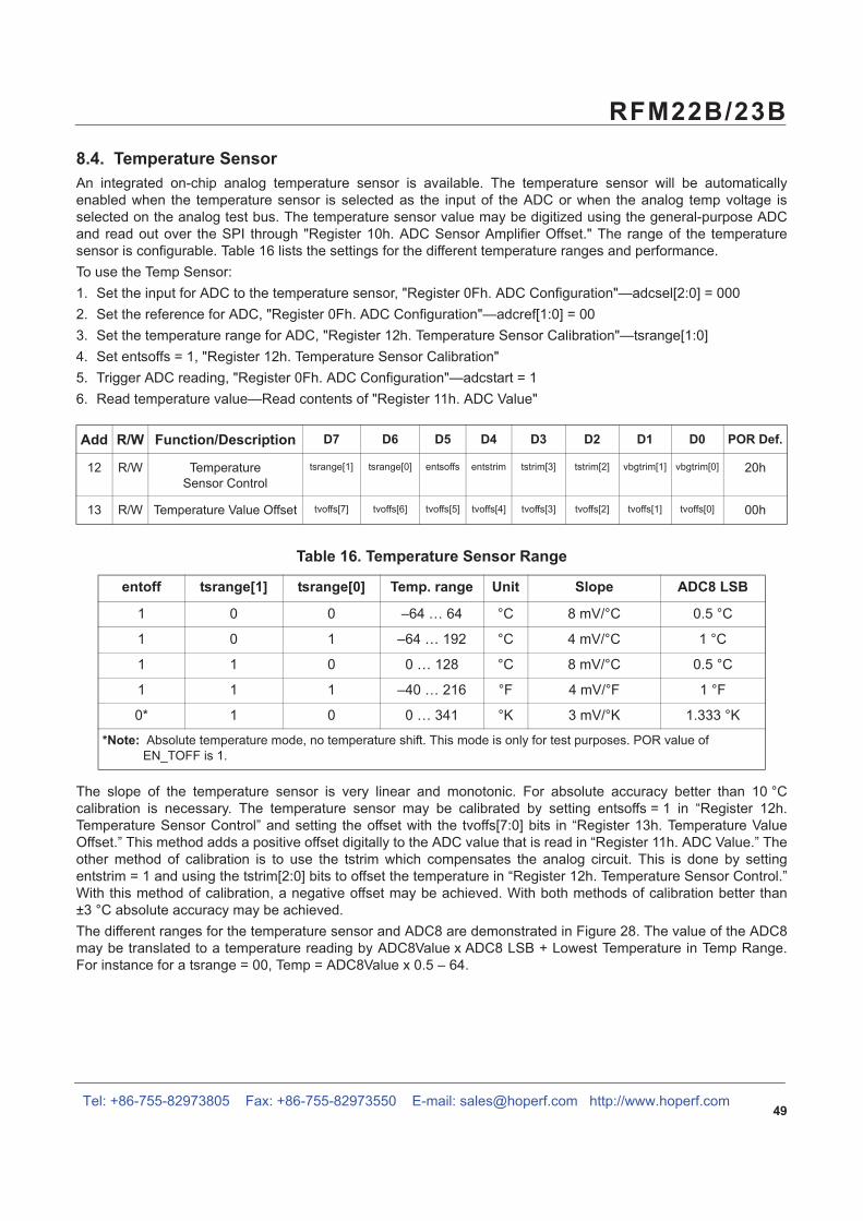
An integrated on-chip analog temperature sensor is available. The temperature sensor will be automatically
enabled when the temperature sensor is selected as the input of the ADC or when the analog temp voltage is
selected on the analog test bus. The temperature sensor value may be digitized using the general-purpose ADC
and read out over the SPI through "Register 10h. ADC Sensor Amplifier Offset." The range of the temperature
sensor is configurable. Table 16 lists the settings for the different temperature ranges and performance.
To use the Temp Sensor:
1. Set the input for ADC to the temperature sensor, "Register 0Fh. ADC Configuration"—adcsel[2:0] = 000
2. Set the reference for ADC, "Register 0Fh. ADC Configuration"—adcref[1:0] = 00
3. Set the temperature range for ADC, "Register 12h. Temperature Sensor Calibration"—tsrange[1:0]
4. Set entsoffs = 1, "Register 12h. Temperature Sensor Calibration"
5. Trigger ADC reading, "Register 0Fh. ADC Configuration"—adcstart = 1
6. Read temperature value—Read contents of "Register 11h. ADC Value"
The slope of the temperature sensor is very linear and monotonic. For absolute accuracy better than 10 °C
calibration is necessary. The temperature sensor may be calibrated by setting entsoffs = 1 in “Register 12h.
Temperature Sensor Control” and setting the offset with the tvoffs[7:0] bits in “Register 13h. Temperature Value
Offset.” This method adds a positive offset digitally to the ADC value that is read in “Register 11h. ADC Value.” The
other method of calibration is to use the tstrim which compensates the analog circuit. This is done by setting
entstrim = 1 and using the tstrim[2:0] bits to offset the temperature in “Register 12h. Temperature Sensor Control.”
With this method of calibration, a negative offset may be achieved. With both methods of calibration better than
±3 °C absolute accuracy may be achieved.
The different ranges for the temperature sensor and ADC8 are demonstrated in Figure 28. The value of the ADC8
may be translated to a temperature reading by ADC8Value x ADC8 LSB + Lowest Temperature in Temp Range.
For instance for a tsrange = 00, Temp = ADC8Value x 0.5 – 64.
12 R/W Temperature
Sensor Control
tsrange[1] tsrange[0] entsoffs entstrim tstrim[3] tstrim[2] vbgtrim[1] vbgtrim[0] 20h
13 R/W Temperature Value Offset tvoffs[7] tvoffs[6] tvoffs[5] tvoffs[4] tvoffs[3] tvoffs[2] tvoffs[1] tvoffs[0] 00h
1 0 0 –64 … 64 °C 8 mV/°C 0.5 °C
1 0 1 –64 … 192 °C 4 mV/°C 1 °C
1 1 0 0 … 128 °C 8 mV/°C 0.5 °C
1 1 1 –40 … 216 °F 4 mV/°F 1 °F
0* 1 0 0 … 341 °K 3 mV/°K 1.333 °K
Absolute temperature mode, no temperature shift. This mode is only for test purposes. POR value of
EN_TOFF is 1.
Tel: +86-755-82973805 Fax: +86-755-82973550 E-mail: [email protected] http://www.hoperf.com

0
50
100
150
200
250
300
-40 -20 0 20 40 60 80 100
Sensor Range 0
Sensor Range 1
Sensor Range 2
Sensor Range 3
Tel: +86-755-82973805 Fax: +86-755-82973550 E-mail: [email protected] http://www.hoperf.com

A low battery detector (LBD) with digital read-out is integrated into the chip. A digital threshold may be programmed
into the lbdt[4:0] field in "Register 1Ah. Low Battery Detector Threshold." When the digitized battery voltage
reaches this threshold an interrupt will be generated on the nIRQ pin to the microcontroller. The microcontroller can
confirm source of the interrupt by reading "Register 03h. Interrupt/Status 1" and “Register 04h. Interrupt/Status 2.”
If the LBD is enabled while the chip is in SLEEP mode, it will automatically enable the RC oscillator which will
periodically turn on the LBD circuit to measure the battery voltage. The battery voltage may also be read out
through "Register 1Bh. Battery Voltage Level" at any time when the LBD is enabled. The low battery detect function
is enabled by setting enlbd=1 in "Register 07h. Operating Mode and Function Control 1".
The LBD output is digitized by a 5-bit ADC. When the LBD function is enabled (enlbd = 1 in "Register 07h.
Operating Mode and Function Control 1") the battery voltage may be read at anytime by reading "Register 1Bh.
Battery Voltage Level." A battery voltage threshold may be programmed in “Register 1Ah. Low Battery Detector
Threshold." When the battery voltage level drops below the battery voltage threshold an interrupt will be generated
on the nIRQ pin to the microcontroller if the LBD interrupt is enabled in “Register 06h. Interrupt Enable 2.” The
microcontroller will then need to verify the interrupt by reading the interrupt status register, addresses 03 and 04h.
The LSB step size for the LBD ADC is 50 mV, with the ADC range demonstrated in the table below. If the LBD is
enabled the LBD and ADC will automatically be enabled every 1 s for approximately 250 µs to measure the voltage
which minimizes the current consumption in Sensor mode. Before an interrupt is activated four consecutive
readings are required.
1A R/W Low Battery Detector Threshold lbdt[4] lbdt[3] lbdt[2] lbdt[1] lbdt[0] 14h
1B R Battery Voltage Level 0 0 0 vbat[4] vbat[3] vbat[2] vbat[1] vbat[0] —
0 < 1.7
1 1.7–1.75
2 1.75–1.8
… …
29 3.1–3.15
30 3.15–3.2
31 > 3.2
ADCValuemVtageBatteryVol 507.1
Tel: +86-755-82973805 Fax: +86-755-82973550 E-mail: [email protected] http://www.hoperf.com

The chip contains an integrated wake-up timer which can be used to periodically wake the chip from SLEEP mode.
The wake-up timer runs from the internal 32.768 kHz RC Oscillator. The wake-up timer can be configured to run
when in SLEEP mode. If enwt = 1 in "Register 07h. Operating Mode and Function Control 1" when entering SLEEP
mode, the wake-up timer will count for a time specified defined in Registers 14–16h, "Wake Up Timer Period." At
the expiration of this period an interrupt will be generated on the nIRQ pin if this interrupt is enabled. The
microcontroller will then need to verify the interrupt by reading the Registers 03h–04h, "Interrupt Status 1 & 2". The
wake-up timer value may be read at any time by the wtv[15:0] read only registers 17h–18h.
The formula for calculating the Wake-Up Period is the following:
Use of the D variable in the formula is only necessary if finer resolution is required than can be achieved by using
the R value.
There are two different methods for utilizing the wake-up timer (WUT) depending on if the WUT interrupt is enabled
in “Register 06h. Interrupt Enable 2.” If the WUT interrupt is enabled then nIRQ pin will go low when the timer
expires. The chip will also change state so that the 30 MHz XTAL is enabled so that the microcontroller clock
output is available for the microcontroller to use to process the interrupt. The other method of use is to not enable
the WUT interrupt and use the WUT GPIO setting. In this mode of operation the chip will not change state until
commanded by the microcontroller. The different modes of operating the WUT and the current consumption
impacts are demonstrated in Figure 29.
A 32 kHz XTAL may also be used for better timing accuracy. By setting the x32 ksel bit in Register 07h "Operating
& Function Control 1", GPIO0 is automatically reconfigured so that an external 32 kHz XTAL may be connected to
this pin. In this mode, the GPIO0 is extremely sensitive to parasitic capacitance, so only the XTAL should be
connected to this pin with the XTAL physically located as close to the pin as possible. Once the x32 ksel bit is set,
all internal functions such as WUT, micro-controller clock, and LDC mode will use the 32 kHz XTAL and not the
32 kHz RC oscillator.
wtr[4:0] R Value in Formula
wtm[15:0] M Value in Formula
14 R/W Wake-Up Timer Period 1 wtr[4] wtr[3] wtr[2] wtr[1] wtr[0] 03h
15 R/W Wake-Up Timer Period 2 wtm[15] wtm[14] wtm[13] wtm[12] wtm[11] wtm[10] wtm[9] wtm[8] 00h
16 R/W Wake-Up Timer Period 3 wtm[7] wtm[6] wtm[5] wtm[4] wtm[3] wtm[2] wtm[1] wtm[0] 00h
17 R Wake-Up Timer Value 1 wtv[15] wtv[14] wtv[13] wtv[12] wtv[11] wtv[10] wtv[9] wtv[8] —
18 R Wake-Up Timer Value 2 wtv[7] wtv[6] wtv[5] wtv[4] wtv[3] wtv[2] wtv[1] wtv[0] —
msM
WUTR
768.32
24
Tel: +86-755-82973805 Fax: +86-755-82973550 E-mail: [email protected] http://www.hoperf.com

Sleep Ready Sleep Ready Sleep Ready Sleep
1 uA
1.5 mA 1.5 mA
Sleep
1 uA
1 uA
1.5 mA
1 uA
Tel: +86-755-82973805 Fax: +86-755-82973550 E-mail: [email protected] http://www.hoperf.com

The Low Duty Cycle Mode is available to automatically wake-up the receiver to check if a valid signal is available.
The basic operation of the low duty cycle mode is demonstrated in the figure below. If a valid preamble or sync
word is not detected the chip will return to sleep mode until the beginning of a new WUT period. If a valid preamble
and sync are detected the receiver on period will be extended for the low duty cycle mode duration (TLDC) to
receive all of the packet. The WUT period must be set in conjunction with the low duty cycle mode duration. The R
value (“Register 14h. Wake-up Timer Period 1”) is shared between the WUT and the TLDC. The ldc[7:0] bits are
located in “Register 19h. Low Duty Cycle Mode Duration.” The time of the TLDC is determined by the formula
below:
msldcTLDCR
768.32
24]0:7[
Tel: +86-755-82973805 Fax: +86-755-82973550 E-mail: [email protected] http://www.hoperf.com

Three general purpose IOs (GPIOs) are available. Numerous functions such as specific interrupts, TRSW control,
Microcontroller Output, etc. can be routed to the GPIO pins as shown in the tables below. When in Shutdown mode
all the GPIO pads are pulled low.
The ADC should not be selected as an input to the GPIO in standby or sleep modes and will cause excess current con-
sumption.
The GPIO settings for GPIO1 and GPIO2 are the same as for GPIO0 with the exception of the 00000 default
setting. The default settings for each GPIO are listed below:
The GPIO drive strength may be adjusted with the gpioXdrv[1:0] bits. Setting a higher value will increase the drive
strength and current capability of the GPIO by changing the driver size. Special care should be taken in setting the
drive strength and loading on GPIO2 when the microcontroller clock is used. Excess loading or inadequate drive
may contribute to increased spurious emissions.
0B R/W GPIO0
Configuration
gpio0drv[1] gpio0drv[0] pup0 gpio0[4] gpio0[3] gpio0[2] gpio0[1] gpio0[0] 00h
0C R/W GPIO1
Configuration
gpio1drv[1] gpio1drv[0] pup1 gpio1[4] gpio1[3] gpio1[2] gpio1[1] gpio1[0] 00h
0D R/W GPIO2
Configuration
gpio2drv[1] gpio2drv[0] pup2 gpio2[4] gpio2[3] gpio2[2] gpio2[1] gpio2[0] 00h
0E R/W I/O Port
Configuration
extitst[2] extitst[1] extitst[0] itsdo dio2 dio1 dio0 00h
GPIO0 POR
GPIO1 POR Inverted
GPIO2 Microcontroller Clock
Tel: +86-755-82973805 Fax: +86-755-82973550 E-mail: [email protected] http://www.hoperf.com

To mitigate the problem of frequency-selective fading due to multi-path propagation, some transceiver systems use
a scheme known as antenna diversity. In this scheme, two antennas are used. Each time the transceiver enters RX
mode the receive signal strength from each antenna is evaluated. This evaluation process takes place during the
preamble portion of the packet. The antenna with the strongest received signal is then used for the remainder of
that RX packet. The same antenna will also be used for the next corresponding TX packet.
This chip fully supports antenna diversity with an integrated antenna diversity control algorithm. The required
signals needed to control an external SPDT RF switch (such as PIN diode or GaAs switch) are available on the
GPIOx pins. The operation of these GPIO signals is programmable to allow for different antenna diversity
architectures and configurations. The antdiv[2:0] bits are found in register 08h “Operating & Function Control 2.”
The GPIO pins are capable of sourcing up to 5 mA of current, so it may be used directly to forward-bias a PIN
diode if desired.
The antenna diversity algorithm will automatically toggle back and forth between the antennas until the packet
starts to arrive. The recommended preamble length for optimal antenna selection is 8 bytes. A special antenna
diversity algorithm (antdiv[2:0] = 110 or 111) is included that allows for shorter preamble lengths for beacon mode in
TDMA-like systems where the arrival of the packet is synchronous to the receiver enable. The recommended
preamble length to obtain optimal antenna selection for synchronous mode is 4 bytes.
08 R/W Operating & Function
Control 2
antdiv[2] antdiv[1] antdiv[0] rxmpk autotx enldm ffclrrx ffclrtx 00h
000 0 1 0 0
001 1 0 0 0
010 0 1 1 1
011 1 0 1 1
100 Antenna Diversity Algorithm 0 0
101 Antenna Diversity Algorithm 1 1
110 Antenna Diversity Algorithm in Beacon Mode 0 0
111 Antenna Diversity Algorithm in Beacon Mode 1 1
Tel: +86-755-82973805 Fax: +86-755-82973550 E-mail: [email protected] http://www.hoperf.com
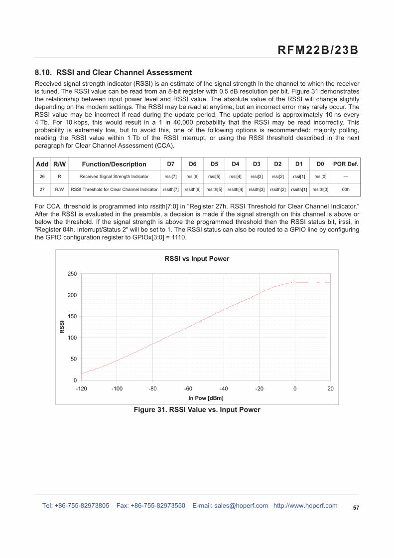
Received signal strength indicator (RSSI) is an estimate of the signal strength in the channel to which the receiver
is tuned. The RSSI value can be read from an 8-bit register with 0.5 dB resolution per bit. Figure 31 demonstrates
the relationship between input power level and RSSI value. The absolute value of the RSSI will change slightly
depending on the modem settings. The RSSI may be read at anytime, but an incorrect error may rarely occur. The
RSSI value may be incorrect if read during the update period. The update period is approximately 10 ns every
4 Tb. For 10 kbps, this would result in a 1 in 40,000 probability that the RSSI may be read incorrectly. This
probability is extremely low, but to avoid this, one of the following options is recommended: majority polling,
reading the RSSI value within 1 Tb of the RSSI interrupt, or using the RSSI threshold described in the next
paragraph for Clear Channel Assessment (CCA).
For CCA, threshold is programmed into rssith[7:0] in "Register 27h. RSSI Threshold for Clear Channel Indicator."
After the RSSI is evaluated in the preamble, a decision is made if the signal strength on this channel is above or
below the threshold. If the signal strength is above the programmed threshold then the RSSI status bit, irssi, in
"Register 04h. Interrupt/Status 2" will be set to 1. The RSSI status can also be routed to a GPIO line by configuring
the GPIO configuration register to GPIOx[3:0] = 1110.
26 R Received Signal Strength Indicator rssi[7] rssi[6] rssi[5] rssi[4] rssi[3] rssi[2] rssi[1] rssi[0] —
27 R/W RSSI Threshold for Clear Channel Indicator rssith[7] rssith[6] rssith[5] rssith[4] rssith[3] rssith[2] rssith[1] rssith[0] 00h
0
50
100
150
200
250
-120 -100 -80 -60 -40 -20 0 20
Tel: +86-755-82973805 Fax: +86-755-82973550 E-mail: [email protected] http://www.hoperf.com
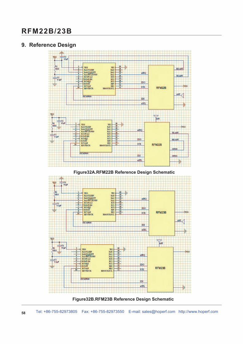
Tel: +86-755-82973805 Fax: +86-755-82973550 E-mail: [email protected] http://www.hoperf.com

00 R Device Type 0 0 0 dt[4] dt[3] dt[2] dt[1] dt[0] 00111
01 R Device Version 0 0 0 vc[4] vc[3] vc[2] vc[1] vc[0] 06h
02 R Device Status ffovfl ffunfl rxffem headerr reserved reserved cps[1] cps[0] —
03 R Interrupt Status 1 ifferr itxffafull itxffaem irxffafull iext ipksent ipkvalid icrcerror —
04 R Interrupt Status 2 iswdet ipreaval ipreainval irssi iwut ilbd ichiprdy ipor —
05 R/W Interrupt Enable 1 enfferr entxffafull entxffaem enrxffafull enext enpksent enpkvalid encrcerror 00h
06 R/W Interrupt Enable 2 enswdet enpreaval enpreainval enrssi enwut enlbd enchiprdy enpor 03h
07 R/W Operating & Function Control 1 swres enlbd enwt x32ksel txon rxon pllon xton 01h
08 R/W Operating & Function Control 2 antdiv[2] antdiv[1] antdiv[0] rxmpk autotx enldm ffclrrx ffclrtx 00h
09 R/W Crystal Oscillator Load Capacitance
xtalshft xlc[6] xlc[5] xlc[4] xlc[3] xlc[2] xlc[1] xlc[0] 7Fh
0A R/W Microcontroller Output Clock Reserved Reserved clkt[1] clkt[0] enlfc mclk[2] mclk[1] mclk[0] 06h
0B R/W GPIO0 Configuration gpio0drv[1] gpio0drv[0] pup0 gpio0[4] gpio0[3] gpio0[2] gpio0[1] gpio0[0] 00h
0C R/W GPIO1 Configuration gpio1drv[1] gpio1drv[0] pup1 gpio1[4] gpio1[3] gpio1[2] gpio1[1] gpio1[0] 00h
0D R/W GPIO2 Configuration gpio2drv[1] gpio2drv[0] pup2 gpio2[4] gpio2[3] gpio2[2] gpio2[1] gpio2[0] 00h
0E R/W I/O Port Configuration Reserved extitst[2] extitst[1] extitst[0] itsdo dio2 dio1 dio0 00h
0F R/W ADC Configuration adcstart/adc-done
adcsel[2] adcsel[1] adcsel[0] adcref[1] adcref[0] adcgain[1] adcgain[0] 00h
10 R/W ADC Sensor Amplifier Offset Reserved Reserved Reserved Reserved adcoffs[3] adcoffs[2] adcoffs[1] adcoffs[0] 00h
11 R ADC Value adc[7] adc[6] adc[5] adc[4] adc[3] adc[2] adc[1] adc[0] —
12 R/W Temperature Sensor Control tsrange[1] tsrange[0] entsoffs entstrim tstrim[3] tstrim[2] tstrim[1] tstrim[0] 20h
13 R/W Temperature Value Offset tvoffs[7] tvoffs[6] tvoffs[5] tvoffs[4] tvoffs[3] tvoffs[2] tvoffs[1] tvoffs[0] 00h
14 R/W Wake-Up Timer Period 1 Reserved Reserved Reserved wtr[4] wtr[3] wtr[2] wtr[1] wtr[0] 03h
15 R/W Wake-Up Timer Period 2 wtm[15] wtm[14] wtm[13] wtm[12] wtm[11] wtm[10] wtm[9] wtm[8] 00h
16 R/W Wake-Up Timer Period 3 wtm[7] wtm[6] wtm[5] wtm[4] wtm[3] wtm[2] wtm[1] wtm[0] 01h
17 R Wake-Up Timer Value 1 wtv[15] wtv[14] wtv[13] wtv[12] wtv[11] wtv[10] wtv[9] wtv[8] —
18 R Wake-Up Timer Value 2 wtv[7] wtv[6] wtv[5] wtv[4] wtv[3] wtv[2] wtv[1] wtv[0] —
19 R/W Low-Duty Cycle Mode Duration ldc[7] ldc[6] ldc[5] ldc[4] ldc[3] ldc[2] ldc[1] ldc[0] 00h
1A R/W Low Battery Detector Threshold Reserved Reserved Reserved lbdt[4] lbdt[3] lbdt[2] lbdt[1] lbdt[0] 14h
1B R Battery Voltage Level 0 0 0 vbat[4] vbat[3] vbat[2] vbat[1] vbat[0] —
1C R/W IF Filter Bandwidth dwn3_bypass ndec[2] ndec[1] ndec[0] filset[3] filset[2] filset[1] filset[0] 01h
1D R/W AFC Loop Gearshift Override afcbd enafc afcgearh[2] afcgearh[1] afcgearh[0] 1p5 bypass matap ph0size 40h
1E R/W AFC Timing Control swait_timer[1] swait_timer[0] shwait[2] shwait[1] shwait[0] anwait[2] anwait[1] anwait[0] 0Ah
1F R/W Clock Recovery Gearshift Override
Reserved Reserved crfast[2] crfast[1] crfast[0] crslow[2] crslow[1] crslow[0] 03h
20 R/W Clock Recovery Oversampling Ratio
rxosr[7] rxosr[6] rxosr[5] rxosr[4] rxosr[3] rxosr[2] rxosr[1] rxosr[0] 64h
21 R/W Clock Recovery Offset 2 rxosr[10] rxosr[9] rxosr[8] stallctrl ncoff[19] ncoff[18] ncoff[17] ncoff[16] 01h
22 R/W Clock Recovery Offset 1 ncoff[15] ncoff[14] ncoff[13] ncoff[12] ncoff[11] ncoff[10] ncoff[9] ncoff[8] 47h
23 R/W Clock Recovery Offset 0 ncoff[7] ncoff[6] ncoff[5] ncoff[4] ncoff[3] ncoff[2] ncoff[1] ncoff[0] AEh
24 R/W Clock Recovery Timing Loop Gain 1
Reserved Reserved Reserved rxncocomp crgain2x crgain[10] crgain[9] crgain[8] 02h
25 R/W Clock Recovery Timing Loop Gain 0
crgain[7] crgain[6] crgain[5] crgain[4] crgain[3] crgain[2] crgain[1] crgain[0] 8Fh
26 R Received Signal Strength Indi-cator
rssi[7] rssi[6] rssi[5] rssi[4] rssi[3] rssi[2] rssi[1] rssi[0] —
27 R/W RSSI Threshold for Clear Channel Indicator
rssith[7] rssith[6] rssith[5] rssith[4] rssith[3] rssith[2] rssith[1] rssith[0] 1Eh
28 R Antenna Diversity Register 1 adrssi1[7] adrssia[6] adrssia[5] adrssia[4] adrssia[3] adrssia[2] adrssia[1] adrssia[0] —
29 R Antenna Diversity Register 2 adrssib[7] adrssib[6] adrssib[5] adrssib[4] adrssib[3] adrssib[2] adrssib[1] adrssib[0] —
2A R/W AFC Limiter Afclim[7] Afclim[6] Afclim[5] Afclim[4] Afclim[3] Afclim[2] Afclim[1] Afclim[0] 00h
2B R AFC Correction Read afc_corr[9] afc_corr[8] afc_corr[7] afc_corr[6] afc_corr[5] afc_corr[4] afc_corr[3] afc_corr[2] 00h
2C R/W OOK Counter Value 1 afc_corr[9] afc_corr[9] ookfrzen peakdeten madeten ookcnt[10] ookcnt[9] ookcnt[8] 18h
2D R/W OOK Counter Value 2 ookcnt[7] ookcnt[6] ookcnt[5] ookcnt[4] ookcnt[3] ookcnt[2] ookcnt[1] ookcnt[0] BCh
2E R/W Slicer Peak Hold Reserved attack[2] attack[1] attack[0] decay[3] decay[2] decay[1] decay[0] 26h
2F Reserved
30 R/W Data Access Control enpacrx lsbfrst crcdonly skip2ph enpactx encrc crc[1] crc[0] 8Dh
Tel: +86-755-82973805 Fax: +86-755-82973550 E-mail: [email protected] http://www.hoperf.com

31 R EzMAC status 0 rxcrc1 pksrch pkrx pkvalid crcerror pktx pksent —
32 R/W Header Control 1 bcen[3:0] hdch[3:0] 0Ch
33 R/W Header Control 2 skipsyn hdlen[2] hdlen[1] hdlen[0] fixpklen synclen[1] synclen[0] prealen[8] 22h
34 R/W Preamble Length prealen[7] prealen[6] prealen[5] prealen[4] prealen[3] prealen[2] prealen[1] prealen[0] 08h
35 R/W Preamble Detection Control preath[4] preath[3] preath[2] preath[1] preath[0] rssi_off[2] rssi_off[1] rssi_off[0] 2Ah
36 R/W Sync Word 3 sync[31] sync[30] sync[29] sync[28] sync[27] sync[26] sync[25] sync[24] 2Dh
37 R/W Sync Word 2 sync[23] sync[22] sync[21] sync[20] sync[19] sync[18] sync[17] sync[16] D4h
38 R/W Sync Word 1 sync[15] sync[14] sync[13] sync[12] sync[11] sync[10] sync[9] sync[8] 00h
39 R/W Sync Word 0 sync[7] sync[6] sync[5] sync[4] sync[3] sync[2] sync[1] sync[0] 00h
3A R/W Transmit Header 3 txhd[31] txhd[30] txhd[29] txhd[28] txhd[27] txhd[26] txhd[25] txhd[24] 00h
3B R/W Transmit Header 2 txhd[23] txhd[22] txhd[21] txhd[20] txhd[19] txhd[18] txhd[17] txhd[16] 00h
3C R/W Transmit Header 1 txhd[15] txhd[14] txhd[13] txhd[12] txhd[11] txhd[10] txhd[9] txhd[8] 00h
3D R/W Transmit Header 0 txhd[7] txhd[6] txhd[5] txhd[4] txhd[3] txhd[2] txhd[1] txhd[0] 00h
3E R/W Transmit Packet Length pklen[7] pklen[6] pklen[5] pklen[4] pklen[3] pklen[2] pklen[1] pklen[0] 00h
3F R/W Check Header 3 chhd[31] chhd[30] chhd[29] chhd[28] chhd[27] chhd[26] chhd[25] chhd[24] 00h
40 R/W Check Header 2 chhd[23] chhd[22] chhd[21] chhd[20] chhd[19] chhd[18] chhd[17] chhd[16] 00h
41 R/W Check Header 1 chhd[15] chhd[14] chhd[13] chhd[12] chhd[11] chhd[10] chhd[9] chhd[8] 00h
42 R/W Check Header 0 chhd[7] chhd[6] chhd[5] chhd[4] chhd[3] chhd[2] chhd[1] chhd[0] 00h
43 R/W Header Enable 3 hden[31] hden[30] hden[29] hden[28] hden[27] hden[26] hden[25] hden[24] FFh
44 R/W Header Enable 2 hden[23] hden[22] hden[21] hden[20] hden[19] hden[18] hden[17] hden[16] FFh
45 R/W Header Enable 1 hden[15] hden[14] hden[13] hden[12] hden[11] hden[10] hden[9] hden[8] FFh
46 R/W Header Enable 0 hden[7] hden[6] hden[5] hden[4] hden[3] hden[2] hden[1] hden[0] FFh
47 R Received Header 3 rxhd[31] rxhd[30] rxhd[29] rxhd[28] rxhd[27] rxhd[26] rxhd[25] rxhd[24] —
48 R Received Header 2 rxhd[23] rxhd[22] rxhd[21] rxhd[20] rxhd[19] rxhd[18] rxhd[17] rxhd[16] —
49 R Received Header 1 rxhd[15] rxhd[14] rxhd[13] rxhd[12] rxhd[11] rxhd[10] rxhd[9] rxhd[8] —
4A R Received Header 0 rxhd[7] rxhd[6] rxhd[5] rxhd[4] rxhd[3] rxhd[2] rxhd[1] rxhd[0] —
4B R Received Packet Length rxplen[7] rxplen[6] rxplen[5] rxplen[4] rxplen[3] rxplen[2] rxplen[1] rxplen[0] —
4C-4E Reserved
4F R/W ADC8 Control Reserved Reserved adc8[5] adc8[4] adc8[3] adc8[2] adc8[1] adc8[0] 10h
50-5F Reserved
60 R/W Channel Filter Coefficient Address
Inv_pre_th[3] Inv_pre_th[2] Inv_pre_th[1] Inv_pre_th[0] chfiladd[3] chfiladd[2] chfiladd[1] chfiladd[0] 00h
61 Reserved
62 R/W Crystal Oscillator/Control Test pwst[2] pwst[1] pwst[0] clkhyst enbias2x enamp2x bufovr enbuf 24h
63-68 Reserved
69 R/W AGC Override 1 Reserved sgi agcen lnagain pga3 pga2 pga1 pga0 20h
6A-6C Reserved
6D R/W TX Power papeakval papeaken papeaklvl[1] papeaklvl[0] Ina_sw txpow[2] txpow[1] txpow[0] 18h
6E R/W TX Data Rate 1 txdr[15] txdr[14] txdr[13] txdr[12] txdr[11] txdr[10] txdr[9] txdr[8] 0Ah
6F R/W TX Data Rate 0 txdr[7] txdr[6] txdr[5] txdr[4] txdr[3] txdr[2] txdr[1] txdr[0] 3Dh
70 R/W Modulation Mode Control 1 Reserved Reserved txdtrtscale enphpwdn manppol enmaninv enmanch enwhite 0Ch
71 R/W Modulation Mode Control 2 trclk[1] trclk[0] dtmod[1] dtmod[0] eninv fd[8] modtyp[1] modtyp[0] 00h
72 R/W Frequency Deviation fd[7] fd[6] fd[5] fd[4] fd[3] fd[2] fd[1] fd[0] 20h
73 R/W Frequency Offset 1 fo[7] fo[6] fo[5] fo[4] fo[3] fo[2] fo[1] fo[0] 00h
74 R/W Frequency Offset 2 Reserved Reserved Reserved Reserved Reserved Reserved fo[9] fo[8] 00h
75 R/W Frequency Band Select Reserved sbsel hbsel fb[4] fb[3] fb[2] fb[1] fb[0] 75h
76 R/W Nominal Carrier Frequency 1 fc[15] fc[14] fc[13] fc[12] fc[11] fc[10] fc[9] fc[8] BBh
77 R/W Nominal Carrier Frequency 0 fc[7] fc[6] fc[5] fc[4] fc[3] fc[2] fc[1] fc[0] 80h
78 Reserved
79 R/W Frequency Hopping Channel Select
fhch[7] fhch[6] fhch[5] fhch[4] fhch[3] fhch[2] fhch[1] fhch[0] 00h
7A R/W Frequency Hopping Step Size fhs[7] fhs[6] fhs[5] fhs[4] fhs[3] fhs[2] fhs[1] fhs[0] 00h
7B Reserved
7C R/W TX FIFO Control 1 Reserved Reserved txafthr[5] txafthr[4] txafthr[3] txafthr[2] txafthr[1] txafthr[0] 37h
7D R/W TX FIFO Control 2 Reserved Reserved txaethr[5] txaethr[4] txaethr[3] txaethr[2] txaethr[1] txaethr[0] 04h
7E R/W RX FIFO Control Reserved Reserved rxafthr[5] rxafthr[4] rxafthr[3] rxafthr[2] rxafthr[1] rxafthr[0] 37h
7F R/W FIFO Access fifod[7] fifod[6] fifod[5] fifod[4] fifod[3] fifod[2] fifod[1] fifod[0] —
Tel: +86-755-82973805 Fax: +86-755-82973550 E-mail: [email protected] http://www.hoperf.com
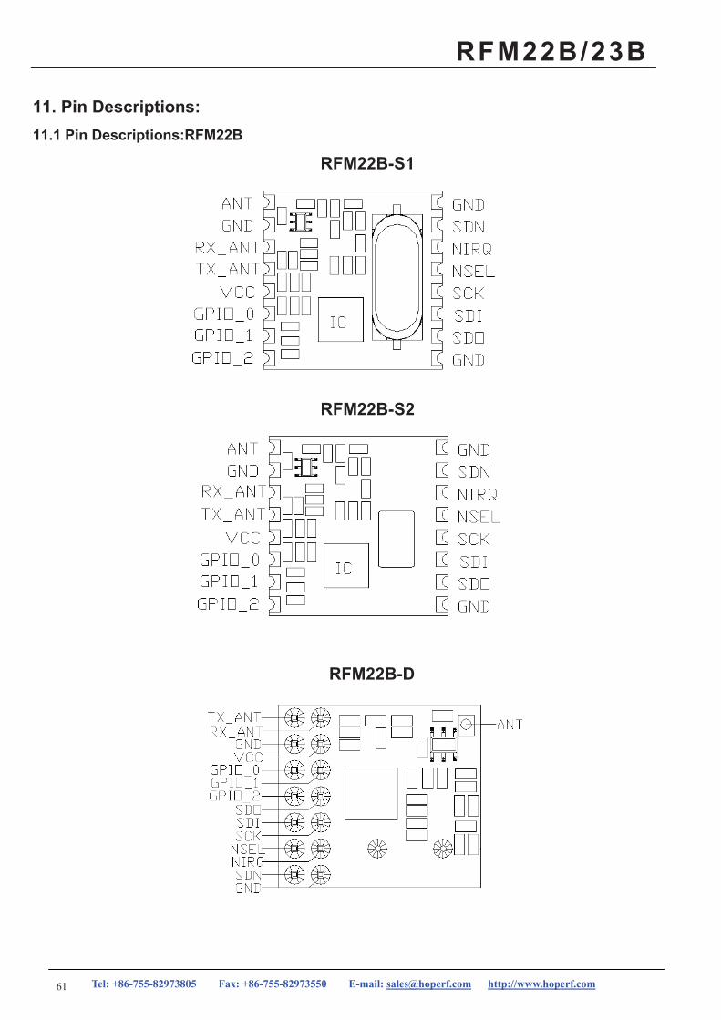
Tel: +86-755-82973805 Fax: +86-755-82973550 E-mail: [email protected] http://www.hoperf.com61

Tel: +86-755-82973805 Fax: +86-755-82973550 E-mail: [email protected] http://www.hoperf.com 62
VCC S +1.8 to +3.6 V supply voltage. The recommended VCC supply voltage is +3.3 V.
GND S Ground reference.
GPIO_0 I/O
GPIO_1 I/O
GPIO_2 I/O
General Purpose Digital I/O that may be configured through the registers to perform various
functions including: Microcontroller Clock Output, FIFO status, POR, Wake-Up timer, Low
Battery Detect, TRSW, AntDiversity control, etc. See the SPI GPIO Configuration Registers,
Address 0Bh, 0Ch, and 0Dh for more information.
SDO O0–VCC V digital output that provides a serial readback function of the internal control
registers.
SDI ISerial Data input. 0–VCC V digital input. This pin provides the serial data stream for the 4-line
serial data bus.
SCLK ISerial Clock input. 0–VDD V digital input. This pin provides the serial data clock function for
the 4-line serial data bus. Data is clocked into the RFM22 on positive edge transitions.
nSEL ISerial Interface Select input. 0– VCC V digital input. This pin provides the Select/Enable
function for the 4-line serial data bus. The signal is also used to signify burst read/write mode.
nIRQ O
General Microcontroller Interrupt Status output. When the RFM22 exhibits anyone of the
Interrupt Events the nIRQ pin will be set low=0. Please see the Control Logic registers
section for more information on the Interrupt Events. The Microcontroller can then determine
the state of the interrupt by reading a corresponding SPI Interrupt Status Registers, Address
03h and 04h.
SDN
I Shutdown input pin. 0–VCC V digital input. SDN should be = 0 in all modes except Shutdown
mode. When SDN =1 the chip will be completely shutdown and the contents of the registers
will be lost.
TX_ANTI Tx Antenna select input pin, When RFM22 is TX state,TX_ANT should be = 1, RX_ANT
should be = 0
RX_ANTI Rx Antenna select input pin, When RFM2 2 is RX state,RX_ANT should be = 1, TX_ANT
should be = 0
ANT I/O RF signal output/input.(50 OHM output /input Impedance)

Tel: +86-755-82973805 Fax: +86-755-82973550 E-mail: [email protected] http://www.hoperf.com63

Tel: +86-755-82973805 Fax: +86-755-82973550 E-mail: [email protected] http://www.hoperf.com 64
VCC S +1.8 to +3.6 V supply voltage. The recommended VCC supply voltage is +3.3 V.
GND S Ground reference.
GPIO_0 I/O
GPIO_1 I/O
GPIO_2 I/O
General Purpose Digital I/O that may be configured through the registers to perform various
functions including: Microcontroller Clock Output, FIFO status, POR, Wake-Up timer, Low
Battery Detect, TRSW, AntDiversity control, etc. See the SPI GPIO Configuration Registers,
Address 0Bh, 0Ch, and 0Dh for more information.
SDO O0–VCC V digital output that provides a serial readback function of the internal control
registers.
SDI ISerial Data input. 0–VCC V digital input. This pin provides the serial data stream for the 4-line
serial data bus.
SCLK ISerial Clock input. 0–VDD V digital input. This pin provides the serial data clock function for
the 4-line serial data bus. Data is clocked into the RFM23A on positive edge transitions.
nSEL ISerial Interface Select input. 0– VCC V digital input. This pin provides the Select/Enable
function for the 4-line serial data bus. The signal is also used to signify burst read/write mode.
nIRQ O
General Microcontroller Interrupt Status output. When the RFM23A exhibits anyone of the
Interrupt Events the nIRQ pin will be set low=0. Please see the Control Logic registers
section for more information on the Interrupt Events. The Microcontroller can then determine
the state of the interrupt by reading a corresponding SPI Interrupt Status Registers, Address
03h and 04h.
SDN
I Shutdown input pin. 0–VCC V digital input. SDN should be = 0 in all modes except Shutdown
mode. When SDN =1 the chip will be completely shutdown and the contents of the registers
will be lost.
NC
NC
ANT I/O RF signal output/input.(50 OHM output /input Impedance)

Tel: +86-755-82973805 Fax: +86-755-82973550 E-mail: [email protected] http://www.hoperf.com65

Tel: +86-755-82973805 Fax: +86-755-82973550 E-mail: [email protected] http://www.hoperf.com 66

Tel: +86-755-82973805 Fax: +86-755-82973550 E-mail: [email protected] http://www.hoperf.com67

Tel: +86-755-82973805 Fax: +86-755-82973550 E-mail: [email protected] http://www.hoperf.com 68

Tel: +86-755-82973805 Fax: +86-755-82973550 E-mail: [email protected]
RFM22B/23B
15. IC Information
70

Tel: +86-755-82973805 Fax: +86-755-82973550 E-mail: [email protected]
RFM22B/23B
16. Package Outline
Figure 33 illustrates the package details for the IC using in the module. Table 19 lists the values for the
dimensions shown in the illustration.
Figure 33. 20-Pin Quad Flat No-Lead (QFN)
Table 19. Package Dimensions
MillimetersSymbol
Min Nom Max
A 0.80 0.85 0.90
A1 0.00 0.02 0.05
b 0.18 0.25 0.30
D 4.00 BSC
D2 2.55 2.60 2.65
e 0.50 BSC
E 4.00 BSC
E2 2.50 2.60 2.70
L 0.30 0.40 0.50
aaa — — 0.10
bbb — — 0.10
ccc — — 0.08
ddd — — 0.10
eee — — 0.10
Notes:
1. All dimensions are shown in millimeters (mm) unless otherwise noted.
2. Dimensioning and tolerancing per ANSI Y14.5M-1994.
3. This drawing conforms to the JEDEC Solid State Outline MO-220,
Variation VGGD-8.
4. Recommended card reflow profile is per the JEDEC/IPC J-STD-020
specification for Small Body Components.
71

Tel: +86-755-82973805 Fax: +86-755-82973550 E-mail: [email protected]
RFM22B/23B
17. PCB Land Pattern
Figure 34 illustrates the PCB land pattern details for the IC using in the module. Table 20 lists the values for
the dimensions shown in the illustration.
Figure 34. PCB Land Pattern
72

Tel: +86-755-82973805 Fax: +86-755-82973550 E-mail: [email protected]
RFM22B/23B
Table 20. PCB Land Pattern Dimensions
MillimetersSymbol
Min Max
C1 3.90 4.00
C2 3.90 4.00
E 0.50 REF
X1 0.20 0.30
X2 2.65 2.75
Y1 0.65 0.75
Y2 2.65 2.75
Notes: General
1. All dimensions shown are in millimeters (mm) unless otherwise noted.
2. This land pattern design is based on IPC-7351 guidelines.
Note: Solder Mask Design
1. All metal pads are to be non-solder mask defined (NSMD). Clearance
between the solder mask and the metal pad is to be 60 µm minimum,
all the way around the pad.
Notes: Stencil Design
1. A stainless steel, laser-cut and electro-polished stencil with trapezoidal
walls should be used to assure good solder paste release.
2. The stencil thickness should be 0.125 mm (5 mils).
3. The ratio of stencil aperture to land pad size should be 1:1 for
the perimeter pads.
4. A 2x2 array of 1.10 x 1.10 mm openings on 1.30 mm pitch should
be used for the center ground pad.
Notes: Card Assembly
1. A No-Clean, Type-3 solder paste is recommended.
2. The recommended card reflow profile is per the JEDEC/IPC J-STD-020
specification for small body components.
73

RFM22B/23B
Add:4/F, Block B3, East Industrial Area,
Huaqiaocheng, Shenzhen, Guangdong, China
Tel: 86-755-82973805
Fax: 86-755-82973550
Email: [email protected]
Website: http://www.hoperf.com
http://hoperf.en.alibaba.com
This document may contain preliminary information and is subject to change by
Hope Microelectronics without notice. Hope Microelectronics assumes no
responsibility or liability for any use of the information contained herein. Nothing
in this document shall operate as an express or implied license or indemnity
under the intellectual property rights of Hope Microelectronics or third parties.
The products described in this document are not intended for use in
implantation or other direct life support applications where malfunction may
result in the direct physical harm or injury to persons. NO WARRANTIES OF
ANY KIND, INCLUDING, BUT NOT LIMITED TO, THE IMPLIED WARRANTIES
OF MECHANTABILITY OR FITNESS FOR A ARTICULAR PURPOSE, ARE
OFFERED IN THIS DOCUMENT.
©2006, HOPE MICROELECTRONICS CO.,LTD. All rights reserved.
Tel: +86-755-82973805 Fax: +86-755-82973550 E-mail: [email protected] http://www.hoperf.com
70


![arXiv:2005.13949v1 [physics.app-ph] 25 May 20207.5 MHz F4 6.5 MHz F5 F6 7.5 MHz F7 F8 6.5 MHz F14 9.5 MHz F15 NA F16 8.5 MHz F17 NA F18 NA F19 7.5 MHz F11 6.5 MHz F20 NA F21 8.5 MHz](https://img.dokumen.tips/doc/110x75/5f758878eb2d114487007824/arxiv200513949v1-25-may-2020-75-mhz-f4-65-mhz-f5-f6-75-mhz-f7-f8-65-mhz.jpg)


![PVCPR11 Edital 3.5 GHz v03.ppt [Modo de Compatibilidade]...2011/06/09 · 35 MHz 35 MHz 10 MHz 10 MHz 10 MHz 10 MHz 10 MHz 10 MHz 3.400,00 MHz 3.600,00 MHz 10 MHz 35 MHz 10 MHz 10](https://img.dokumen.tips/doc/110x75/5f7286506e7f433bb4685297/pvcpr11-edital-35-ghz-v03ppt-modo-de-compatibilidade-20110609-35-mhz.jpg)