Embed Size (px)
Citation preview

2016.03.09.
1
1
DIGITAL TECHNICS II
Dr. Bálint Pődör
Óbuda University,
Microelectronics and Technology Institute
5. LECTURE: ANALYSIS AND SYNTHESIS OF
SYNCHRONOUS SEQUENTIAL CIRCUITS
2nd (Spring) term 2015/2016
2
5. LECTURE
Analysis and synthesis of
synchronous sequential circuits:
Design examples and case studies

2016.03.09.
2
SYNTHESIS: GENERAL CONCEPTS
Synchronous sequential circuits synthesis procedure
Word description of problem (hardest; art, not science)
Derive state diagram and state table
Minimize (moderately hard)
Assign states (very hard)
Produce state and output transition tables
Determine what FFs to use and find their excitation maps
Derive output equations/K-maps
Obtain the logic diagram
This is the so called ”next state method” (c.f. Zsom Vol II)
INTRODUCTORY EXAMPLES
4
Control of an alarm system – role of memory
Two-flip-flop circuit - designing with next-state

2016.03.09.
3
EXAMPLE 1: CONTROL OF AN
ALARM SYSTEM
5
Sensor Memory
element Alarm
Set
Reset
__
On/Off
Control of an alarm system is one of the simplest case of
sequential logic.
Alarm is ON when the sensor generates a positive voltage,
SET, in response to an undesirable event.
Once alarm is on, it can only be turned off manually
through a RESET button.
Memory is needed to remember the alarm has to be active
until the reset signal arrives.
EXAMPLE 1: APPLICATION OF THE
SR LATCH – An important application of SR latches is for recording
short lived events
• e.g. pressing an alarm bell in a hospital
RS
Latch
R
S
Q
RS
Latch
R
S
Q
bed1
light
bed2
light
warning
bell
bed1
button
bed2
button
master
reset
1
1
1

2016.03.09.
4
SYNTHESIS OF SYNCHRONOUS
SEQUENTIAL CIRCUIT: EXAMPLE 2
7
Synthesize the synchronous circuit which
operates according to the given state
table.
E.g. if the system in state C and the X
input variable is 1, then in the next clock
period the system goes to state D and the
output variable will take the value 0.
STATE TRANSITION DIAGRAM
8
A B C
D
1/0 1/1
1/0
0/0
0/1
0/0 0/0
1/0

2016.03.09.
5
9
SYNTHESIS: EXAMPLE 2
• Example:
– Find D FF
realization of
circuit defined
in table (a)
– (b): state
assignment
– (c): transition
table
– (d): output K-
map
– (e): excitation
K-map
STATE ENCODING
10

2016.03.09.
6
FLIP-FOP CONTROL: D-FF
11
12
IMPLEMENTATION
• Example
solution:
– Logic
diagram
x
z
Clock

2016.03.09.
7
13
SYNTHESIS WITH JK FLIP-FLOPS
(a): transition table; (b): Excitation tables; (c): Excitation maps
Example is same
as before, but use
JK FFs
SYNTHESIS: JK FLIP-FLOP
14

2016.03.09.
8
FLIP-FLOP-1 CONTROL
15
FLIP-FLOP-2 CONTROL
16

2016.03.09.
9
17
IMPLEMENTATION
• Example JK FF
solution:
– Logic diagram
J1 = X Y2
_
K1 = X Y2
_ __
J2 = X Y1 + X Y1
_ __
K2 = X Y1 + X Y1
x
Clock
z
18
COMPARISON OF TWO DESIGNS
x x
Clock Clock
z z

2016.03.09.
10
COMPARISON OF DIFFERENT DESIGNS
19
Flip-flop: D D JK JK
Logic: AND-OR XOR AND-OR XOR
Pin count: 20 16 28 15
Gate count: 9 7 11 7
20
SYNTHESIS OF SYNCHRONOUS CIRCUITS:
GENERAL PROCEDURE (EMPHASIS)
1. Constructing the state transition diagram.
2. Selection or specifying the encoding of the states.
3. Constructing the state transition tables. It gives for each
cycle the next-state of each flip-flop in the function of the
previous states of all flip-flops and in the function of the
control conditions (up/down).
4. Selection or specifying the type of flip-flop used in the
implementation. Excitation table of the flip-flop type.
5. Determination of the logic functions of the control input(s)
of each flip-flop. Performing the necessary or appropriate
minimization.
6. Selection of the types of logic gates to be used and
implementation of the feedback/control network.

2016.03.09.
11
STATE MACHINE
21 General scheme of a state machine.
STATE MACHINE SYNTHESIS
22
The strategy for applying this scheme to a given problem
consists of the following:
1. Identify the number of required states, m. The number
of bits of memory (e.g. number of flip-flops) required to
specify the m states is at minimum n = log2(m).
2. Make a state diagram which shows all states, inputs,
and outputs.
3. Make a truth table for the logic section. The table will
have n + k inputs and n + m outputs.
4. Implement the truth table using combinational logic
techniques.

2016.03.09.
12
23
SYNTHESIS OF SEQUENTIAL CIRCUIT:
A CASE STUDY
• Synthetize a network which determines the parity of a four
bit serial code word.
• Should indicate the parity of the incoming code word
after receiving the 4-th bit as
- 1 if the parity is odd,
- 0 if the parity is even.
• The output is irrelevant (don’t care) during the first three
cycle of the period.
24
4-BIT PARITY INDICATOR
• When checking the parity the order of the bits is irrelevant.
• Construct the state transition diagram of the
Mealy-machine.
Mealy
machine

2016.03.09.
13
25
4-BIT PARITY INDICATOR:
STATE TRANSITION DIAGRAM
left (s)- even
right (n) - odd
red - incoming bit 0
green - incoming bit 1
The output Z is defined only
in the fourth cycle, otherwise
it is ”don’t care”.
For the code word 1011
a c d f a
even odd
26
CHARACTERISTICS
• Because there are two input conditions, two connecting
lines emanate from each node.
• The network returns to its initial state after the fourth cycle.
• The operation of the network is cyclic, the length of the
period is four cycles.

2016.03.09.
14
27
STATE TRANSITION TABLE AND
DIAGRAM
even odd
28
THE NUMBER OF INTERNAL STATES
AND THEIR ENCODING
• Total number of internal states: seven
• Three flip-flops (Q1, Q2, Q3) are necessary and
enough for the encoding.
• The actual state encoding greatly influences the
complexity and structure of the network.
• Here we use the final (optimal) state encoding.

2016.03.09.
15
29
STATE ENCODING
• In the firs row, we make use of
the redundancy.
• To the states in the same level
of the state transition diagram,
the same Q1 and Q2 codes are
ascribed.
• Q1, Q2: cycle counters.
• Q3: indicates whether the
system is in the even or on the
odd branch of the state transition
diagram.
30
STATE FUNCTIONS AND THE OUTPUT
FUNCTION

2016.03.09.
16
31
STATE FUNCTIONS AND THE OUTPUT
FUNCTION
32
STATE FUNCTIONS AND THE OUTPUT
FUNCTION
Q1n+1 = 4(2,3,6,7,10,11,14,15);
Q2n+1 = 4(0-3,8-12);
Q3n+1 = 4(3,7,8,9,10); x:(4,5,12,13);
Zn = 4(5,12); x:(0-3,6-11,14,15);
The weighing of
the variables:
Xn 8
Q1n 4
Q2n 2
Q3n 1

2016.03.09.
17
33
EXCITATION TABLE
OF THE JK FLIP-FLOP
The logic synthesis is based on the excitation table of the flip-
flop chosen for the implementation.
Qn Qn+1 J K
——————————————
0 0 0 X
0 1 1 X
1 0 X 1
1 1 X 0
34
CONTROL OF FLIP-FLOP Q1
_
K1 = Q2 J1 = Q2 Note the role of the don’t care terms in the minimization.

2016.03.09.
18
35
CONTROL OF FLIP-FLOP Q2
_
K2 = Q1 J2 = Q1 Due to the proper state-encoding, the X input variable is not
present in the control equations of Q1 és Q2 .These two flip-
flops act as cycle counter.
36
CONTROL OF FLIP-FLOP Q3
_ _ _
K3 = X Q2 + X Q2 = X Q2 J3 = X
The X input is among the variables controlling the flip-flop. The
state of Q3 will represent the actual parity. Q3 will “remember”
then parity of the input sequence.
2016.03.09.
19
37
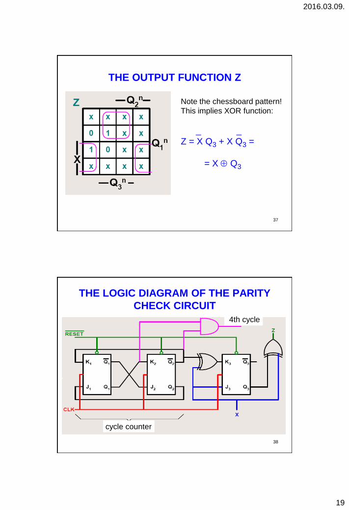
THE OUTPUT FUNCTION Z
Note the chessboard pattern!
This implies XOR function:
_ _
Z = X Q3 + X Q3 =
= X Q3
38
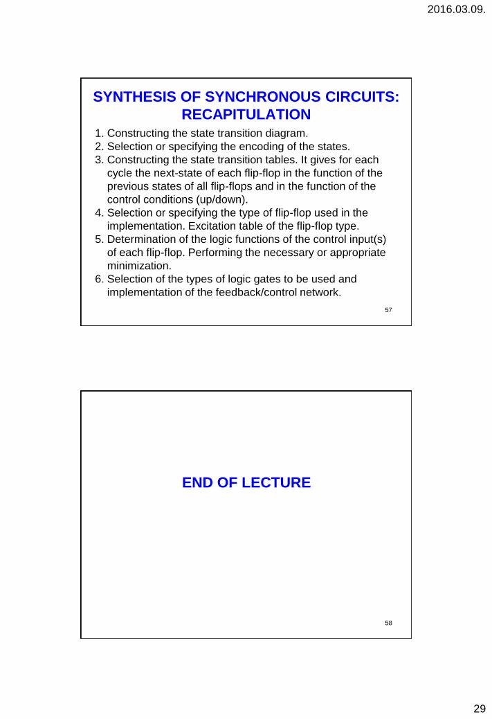
THE LOGIC DIAGRAM OF THE PARITY
CHECK CIRCUIT
cycle counter
4th cycle

2016.03.09.
20
39
IMPLEMENTATION ALTERNATIVE USING
D FLIP-FLOPS
_
D1 = Q2 D2 = Q1
_ _ _
D3 = X Q1 + X Q3 + X Q1 Q2
Due to the ”clever” sate encoding, the control of the two flip-
flops acting as the cycle counter corresponds to the usual
one. However the control network of the third flip-flop is
somewhat more complex than in the former implementation.
40
IMPLEMENTATION USING T FLIP-FLOPS
The feedback network is somewhat more complicated than
in the case of D flip-flops.
Main reason: Counting in Gray code with T flip-flops needs
more gates for the feedback.
Perhaps somebody might check a design with T flip-flops,
the cycle counter operating in the simple binary code…

2016.03.09.
21
8-BIT PARITY INDICATOR
41
Generalization to 8 bit s is straightforward.
Design procedure and the state transition diagram is similar.
There will be 15 states, therefore four flip-flops are
necessary. If the encoding is the same as previously, then
three FFs form the cycle counter, and the fourth will store the
information concerning the parity.
8-BIT PARITY INDICATOR
42
State transition diagram
Input 0 Input 1

2016.03.09.
22
8-BIT PARITY INDICATOR
43 State table and encoding
8-BIT PARITY INDICATOR: LOGIC DIAGRAM
44

2016.03.09.
23
SYNCHRONOUS COUNTER
DESIGN EXAMPLE AND CASE STUDY
45
Consider the synthesis of a 4-bit up-counter in Gray-code
using D flip-flops.
A Gray-code counter using D flip-flops can be designed by
finding the appropriate function of each D terminal. Given a
present state of the counter, the D terminal of each flip-flop
should be made equal to the value of the same bit position
of the next-number in the Gray code.
4-BIT GRAY CODE COUNTER:
CONCEPTUAL DIAGRAM
46
Q3
D3
Q2
D2
Q1
D1
Q0
D3
Combinational feedback circuit
4
Clock

2016.03.09.
24
STATE TRANSITION TABLE
47
Minterm
index
Q3n Q2n Q1n Q0n Q3n+1
D3
Q2 n+1
D2
Q1 n+1
D1
Q0 n+1
D0
0
1
3
2
0
0
0
0
0
0
0
0
0
0
1
1
0
1
1
0
0
0
0
0
0
0
0
1
0
1
1
1
1
1
0
0
6
7
5
4
0
0
0
0
1
1
1
1
1
1
0
0
0
1
1
0
0
0
0
1
1
1
1
1
1
0
0
0
1
1
0
0
12
13
15
14
1
1
1
1
1
1
1
1
0
0
1
1
0
1
1
0
1
1
1
1
1
1
1
0
0
1
1
1
1
1
0
0
10
11
9
8
1
1
1
1
1
1
1
0
1
1
0
0
0
1
1
0
1
1
1
0
0
0
0
0
1
0
0
0
1
1
0
0
KARNAUGH MAPPING
48
D3 D2

2016.03.09.
25
KARNAUGH MAPPING
49
D1 D0
FLIP-FLOP CONTROL EQUATIONS
50
__ __
Q3n+1 = D3 = Q3Q0 + Q3Q1 + Q2Q1Q0
__ __ __
Q2n+1 = D2 = Q2Q1 + Q2Q0 + Q3Q1Q0
__ __ __
Q1n+1 = D1 = Q1Q0 +Q3Q2Q0 + Q3Q2Q0
__ __ __ __ __ __
Q0n+1 = D0 = Q3Q2Q1 +Q3Q2Q1 +Q3Q2Q1 +Q3Q2Q1
Implementation options: two-level AND-OR (13 AND, 4 OR)
in modular logic or PLA, or two-level NAND-NAND in
modular logic, or PROM.

2016.03.09.
26
FLIP-FLOP CONTROL EQUATIONS
51
Design alternative: D1 and D0 controls can be implemented in
AND-OR-XOR LOGIC too.
__ __ __
Q1n+1 = D1 = Q1Q0 +Q3Q2Q0 + Q3Q2Q0 =
__ __
Q1Q0 + (Q3Q2)Q0
__ __ __ __ __ __
Q0n+1 = D0 = Q3Q2Q1 +Q3Q2Q1 +Q3Q2Q1 +Q3Q2Q1 =
__
Q3Q2Q1
Give a three-level combinational network (7 AND, 3 OR, 2
XOR, and 1 INV).
UP/DOWN 3-BIT GRAY CODE COUNTER
52
State transition diagram
Next-state table
_____
UP/DOWN control input: Y

2016.03.09.
27
UP/DOWN 3-BIT GRAY CODE COUNTER
53
Variables: Q2, Q1, Q0, and Y
UP/DOWN 3-BIT GRAY CODE COUNTER
54
Logic expressions for flip-flop control

2016.03.09.
28
UP/DOWN 3-BIT GRAY CODE COUNTER
55
4-BIT BI-DIRECTIONAL
GRAY CODE COUNTER
56
Features of design provided by one of the students of my
previous course.
Compared designs using D or T flip-flops.
Using T flip-flops, some several common terms could be
realized by XOR gate or XOR gate and inverter, leading to
further simplification of the feedback circuit.
Complexity: 16 NAND gates (2,3 or 4 inputs), 2 XOR gates
and 2 inverters.
Estimated the maximum clock frequency of the counter when
using high speed CMOS logic components.
2016.03.09.
29
57
SYNTHESIS OF SYNCHRONOUS CIRCUITS:
RECAPITULATION
1. Constructing the state transition diagram.
2. Selection or specifying the encoding of the states.
3. Constructing the state transition tables. It gives for each
cycle the next-state of each flip-flop in the function of the
previous states of all flip-flops and in the function of the
control conditions (up/down).
4. Selection or specifying the type of flip-flop used in the
implementation. Excitation table of the flip-flop type.
5. Determination of the logic functions of the control input(s)
of each flip-flop. Performing the necessary or appropriate
minimization.
6. Selection of the types of logic gates to be used and
implementation of the feedback/control network.
58
END OF LECTURE


![11. Mérés - mti.kvk.uni-obuda.humti.kvk.uni-obuda.hu/adat/tananyag/elektronika4/E4_11_csomeres_v5a.pdf · 2·10-6·U A 3/2 = K·U A 3/2 [Amper] Ahol d az anód-katód közötti](https://img.dokumen.tips/doc/110x75/5ce266e588c993c0528c42c8/11-meres-mtikvkuni-obudahumtikvkuni-obudahuadattananyagelektronika4e411csomeresv5apdf.jpg)


