Embed Size (px)
Citation preview

125
5.1 INTRODUCTION
The digital system consists of two types of circuits, namely
(i) Combinational circuits and
(ii) Sequential circuits
A combinational circuit consists of logic gates, where outputs are at any instant and are determined only by the present combination of inputs without regard to previous inputs or previous state of outputs. A combinational circuit performs a specifi c information-processing operation assigned logically by a set of Boolean functions. Sequential circuits contain logic gates as well as memory cells. Their outputs depend on the present inputs and also on the states of memory elements. Since the outputs of sequential circuits depend not only on the present inputs but also on past inputs, the circuit behavior must be specifi ed by a time sequence of inputs and memory states. The sequential circuits will be discussed later in the chapter.
In the previous chapters we have discussed binary numbers, codes, Boolean algebra and simplifi cation of Boolean function, logic gates, and economical gate implementation. Binary numbers and codes bear discrete quantities of information and the binary variables are the representation of electric voltages or some other signals. In this chapter, formulation and analysis of various systematic design of combinational circuits and application of information- processing hardware will be discussed.
Figure 5.1
A combinational circuit consists of input variables, logic gates, and output variables. The logic gates accept signals from inputs and output signals are generated according to the logic
Combinationa l
Log icC ircu it
.
.
.
.
..
.
.
m output
variab les
n inpu t
variab les
COMBINATIONAL
LOGIC CIRCUITS5C h a p t e r

126 DIGITAL PRINCIPLES AND LOGIC DESIGN
circuits employed in it. Binary information from the given data transforms to desired output data in this process. Both input and output are obviously the binary signals, i.e., both the input and output signals are of two possible states, logic 1 and logic 0. Figure 5.1 shows a block diagram of a combinational logic circuit. There are n number of input variables coming from an electric source and m number of output signals go to an external destination. The source and/or destination may consist of memory elements or sequential logic circuit or shift registers, located either in the vicinity of the combinational logic circuit or in a remote external location. But the external circuit does not interfere in the behavior of the combinational circuit.
For n number of input variables to a combinational circuit, 2n possible combinations of binary input states are possible. For each possible combination, there is one and only one possible output combination. A combinational logic circuit can be described by m Boolean functions and each output can be expressed in terms of n input variables.
5.2 DESIGN PROCEDURE
Any combinational circuit can be designed by the following steps of design procedure.
1. The problem is stated. 2. Identify the input variables and output functions. 3. The input and output variables are assigned letter symbols. 4. The truth table is prepared that completely defi nes the relationship between the input
variables and output functions. 5. The simplifi ed Boolean expression is obtained by any method of minimization—algebraic
method, Karnaugh map method, or tabulation method. 6. A logic diagram is realized from the simplifi ed expression using logic gates.
It is very important that the design problem or the verbal specifi cations be interpreted correctly to prepare the truth table. Sometimes the designer must use his intuition and experience to arrive at the correct interpretation. Word specifi cation are very seldom exact and complete. Any wrong interpretation results in incorrect truth table and combinational circuit.
Varieties of simplifi cation methods are available to derive the output Boolean functions from the truth table, such as the algebraic method, the Karnaugh map, and the tabulation method. However, one must consider different aspects, limitations, restrictions, and criteria for a particular design application to arrive at suitable algebraic expression. A practical design approach should consider constraints like—(1) minimum number of gates, (2) minimum number of outputs, (3) minimum propagation time of the signal through a circuit, (4) minimum number of interconnections, and (5) limitations of the driving capabilities of each logic gate. Since the importance of each constraint is dictated by the particular application, it is diffi cult to make all these criteria satisfi ed simultaneously, and also diffi cult to make a general statement on the process of achieving an acceptable simplifi cation. However, in most cases, fi rst the simplifi ed Boolean expression at standard form is derived and then other constraints are taken care of as far as possible for a particular application.
5.3 ADDERS
Various information-processing jobs are carried out by digital computers. Arithmetic operations are among the basic functions of a digital computer. Addition of two binary digits is the
COMBINATIONAL LOGIC CIRCUITS 127
most basic arithmetic operation. The simple addition consists of four possible elementary operations, which are 0+0 = 0, 0+1 = 1, 1+0 = 1, and 1+1 = 10. The fi rst three operations produce a sum of one digit, but the fourth operation produces a sum consisting of two digits. The higher signifi cant bit of this result is called the carry. A combinational circuit that performs the addition of two bits as described above is called a half-adder. When the augend and addend numbers contain more signifi cant digits, the carry obtained from the addition of two bits is added to the next higher-order pair of signifi cant bits. Here the addition operation involves three bits—the augend bit, addend bit, and the carry bit and produces a sum result as well as carry. The combinational circuit performing this type of addition operation is called a full-adder. In circuit development two half-adders can be employed to form a full-adder.
5.3.1 Design of Half-adders
As described above, a half-adder has two inputs and two outputs. Let the input variables augend and addend be designated as A and B, and output functions be designated as S for sum and C for carry. The truth table for the functions is below.
Input variables Output variables
A B S C
0 0 0 0
0 1 1 0
1 0 1 0
1 1 0 1
Figure 5.2
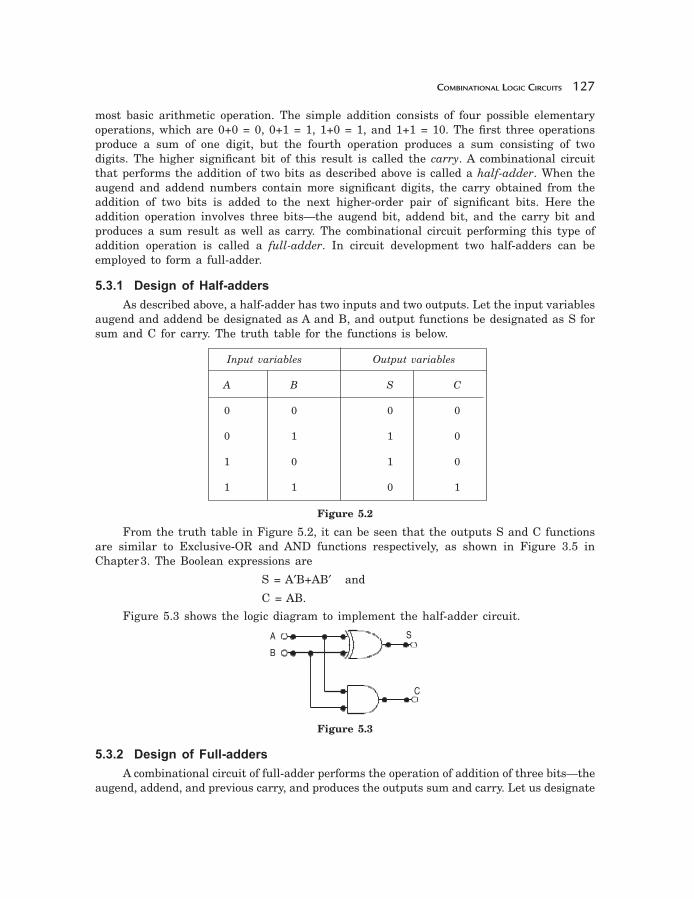
From the truth table in Figure 5.2, it can be seen that the outputs S and C functions are similar to Exclusive-OR and AND functions respectively, as shown in Figure 3.5 in Chapter 3. The Boolean expressions are
S = A′B+AB′ and
C = AB.
Figure 5.3 shows the logic diagram to implement the half-adder circuit.
Figure 5.3
5.3.2 Design of Full-adders
A combinational circuit of full-adder performs the operation of addition of three bits—the augend, addend, and previous carry, and produces the outputs sum and carry. Let us designate
A
B
S
C

128 DIGITAL PRINCIPLES AND LOGIC DESIGN
the input variables augend as A, addend as B, and previous carry as X, and outputs sum as S and carry as C. As there are three input variables, eight different input combinations are possible. The truth table is shown in Figure 5.4 according to its functions.
Input variables Outputs
X A B S C
0 0 0 0 0
0 0 1 1 0
0 1 0 1 0
0 1 1 0 1
1 0 0 1 0
1 0 1 0 1
1 1 0 0 1
1 1 1 1 1
Figure 5.4
To derive the simplifi ed Boolean expression from the truth table, the Karnaugh map method is adopted as in Figures 5.5(a)-(b).
A′B′ A′B AB AB′ A′B′ A′B AB AB′
X′ 1 1 X′ 1
X 1 1 X 1 1 1
Figure 5.5(a) Map for function S. Figure 5.5(b) Map for function C.
The simplifi ed Boolean expressions of the outputs are
S = X′A′B + X′AB′ + XA′B′ + XAB and
C = AB + BX + AX.
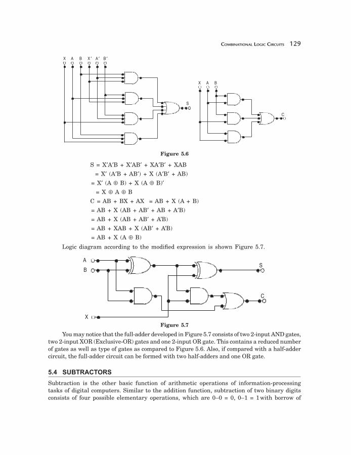
The logic diagram for the above functions is shown in Figure 5.6. It is assumed complements of X, A, and B are available at the input source.
Note that one type of confi guration of the combinational circuit diagram for full-adder is realized in Figure 5.6, with two-input and three-input AND gates, and three input and four-input OR gates. Other confi gurations can also be developed where number and type of gates are reduced. For this, the Boolean expressions of S and C are modifi ed as followo.
COMBINATIONAL LOGIC CIRCUITS 129
Figure 5.6
S = X′A′B + X′AB′ + XA′B′ + XAB
= X′ (A′B + AB′) + X (A′B′ + AB)
= X′ (A ⊕ B) + X (A ⊕ B)′ = X ⊕ A ⊕ B C = AB + BX + AX = AB + X (A + B)
= AB + X (AB + AB′ + AB + A′B)
= AB + X (AB + AB′ + A’B)
= AB + XAB + X (AB′ + A’B)
= AB + X (A ⊕ B)
Logic diagram according to the modifi ed expression is shown Figure 5.7.
Figure 5.7
You may notice that the full-adder developed in Figure 5.7 consists of two 2-input AND gates, two 2-input XOR (Exclusive-OR) gates and one 2-input OR gate. This contains a reduced number of gates as well as type of gates as compared to Figure 5.6. Also, if compared with a half-adder circuit, the full-adder circuit can be formed with two half-adders and one OR gate.
5.4 SUBTRACTORS
Subtraction is the other basic function of arithmetic operations of information-processing tasks of digital computers. Similar to the addition function, subtraction of two binary digits consists of four possible elementary operations, which are 0–0 = 0, 0–1 = 1 with borrow of
X A B X ′ A ′ B ′
C
S
X A B
B
AS
X
C

130 DIGITAL PRINCIPLES AND LOGIC DESIGN
1, 1–0 = 1, and 1–1 = 0. The fi rst, third, and fourth operations produce a subtraction of one digit, but the second operation produces a difference bit as well as a borrow bit. The borrow bit is used for subtraction of the next higher signifi cant bit. A combinational circuit that performs the subtraction of two bits as described above is called a half-subtractor. The digit from which another digit is subtracted is called the minuend and the digit which is to be subtracted is called the subtrahend. When the minuend and subtrahend numbers contain more signifi cant digits, the borrow obtained from the subtraction of two bits is subtracted from the next higher-order pair of signifi cant bits. Here the subtraction operation involves three bits—the minuend bit, subtrahend bit, and the borrow bit, and produces a different result as well as a borrow. The combinational circuit that performs this type of addition operation is called a full-subtractor. Similar to an adder circuit, a full-subtractor combinational circuit can be developed by using two half-subtractors.
5.4.1 Design of Half-subtractors
A half-subtractor has two inputs and two outputs. Let the input variables minuend and subtrahend be designated as X and Y respectively, and output functions be designated as D for difference and B for borrow. The truth table of the functions is as follows.
Input variables Output variables
X Y D B
0 0 0 0
0 1 1 1
1 0 1 0
1 1 0 0
Figure 5.8
By considering the minterms of the truth table in Figure 5.8, the Boolean expressions of the outputs D and B functions can be written as
D = X′Y + XY′ and
B = X′Y.
Figure 5.9 shows the logic diagram to realize the half-subtractor circuit.
Figure 5.9
X
Y
D
B

COMBINATIONAL LOGIC CIRCUITS 131
5.4.2 Design of Full-subtractors
A combinational circuit of full-subtractor performs the operation of subtraction of three bits—the minuend, subtrahend, and borrow generated from the subtraction operation of previous signifi cant digits and produces the outputs difference and borrow. Let us designate the input variables minuend as X, subtrahend as Y, and previous borrow as Z, and outputs difference as D and borrow as B. Eight different input combinations are possible for three input variables. The truth table is shown in Figure 5.10(a) according to its functions.
Input variables Outputs
X Y Z D B
0 0 0 0 0
0 0 1 1 1
0 1 0 1 1
0 1 1 0 1
1 0 0 1 0
1 0 1 0 0
1 1 0 0 0
1 1 1 1 1
Figure 5.10(a)
Y′Z′ Y′Z YZ YZ′ Y′Z′ Y′Z YZ YZ′
X′ 1 1 X′ 1 1 1
X 1 1 X 1
Figure 5.10(b) Map for function D. Figure 5.10(c) Map for function B.
Karnaugh maps are prepared to derive simplifi ed Boolean expressions of D and B as in Figures 5.10(b) and 5.10(c), respectively.
The simplifi ed Boolean expressions of the outputs are
S = X′Y′Z + X′YZ′ + XY′Z′ + XYZ and
C = X′Z + X′Y + YZ.
The logic diagram for the above functions is shown in Figure 5.11.
Similar to a full-adder circuit, it should be noticed that the confi guration of the combinational circuit diagram for full-subtractor as shown in Figure 5.11 contains two-input and three-input AND gates, and three-input and four-input OR gates. Other confi gurations can also be developed where number and type of gates are reduced. For this, the Boolean expressions of D and B are modifi ed as follows.

132 DIGITAL PRINCIPLES AND LOGIC DESIGN
Figure 5.11
D = X′Y′Z + X′YZ′ + XY′Z′ + XYZ
= X′ (Y′Z + YZ′) + X (Y′Z′ + YZ)
= X′ (Y⊕Z) + X (Y⊕Z)′ = X⊕Y⊕Z
B = X′Z + X′Y +YZ = X′Y + Z (X′ + Y)
= X′Y + Z(X′Y + X′Y′ + XY + X′Y)
= X′Y + Z(X′Y + X′Y′ + XY)
= X′Y + X′YZ + Z(X′Y′ + XY)
= X′Y + Z(X⊕Y)′Logic diagram according to the modifi ed expression is shown in Figure 5.12.
Figure 5.12
Note that the full-subtractor developed in Figure 5.12 consists of two 2-input AND gates, two 2-input XOR (Exclusive-OR) gates, two INVERTER gates, and one 2-input OR gate. This contains a reduced number of gates as well as type of gates as compared to Figure 5.12. Also, it may be observed, if compared with a half-subtractor circuit, the full-subtractor circuit can be developed with two half-subtractors and one OR gate.
5.5 CODE CONVERSION
We have seen in Chapter 2 that a large variety of codes are available for the same discrete elements of information, which results in the use of different codes for different digital
X Y Z X ′ Y ′ Z ′
D
X ′
B
Y Z
X
Z
YD
B
COMBINATIONAL LOGIC CIRCUITS 133
systems. It is sometimes necessary to interface two digital blocks of different coding systems. A conversion circuit must be inserted between two such digital systems to use information of one digital system to other. Therefore, a code converter circuit makes two systems compatible when two systems use different binary codes.
To convert from one binary code A to binary code B, the input lines must provide the bit combination of elements as specifi ed by A and the output lines must generate the corresponding bit combinations of code B. A combinational circuit consisting of logic gates performs this transformation operation. Some specifi c examples of code conversion techniques are illustrated in this chapter.
5.5.1 Binary-to-gray Converter
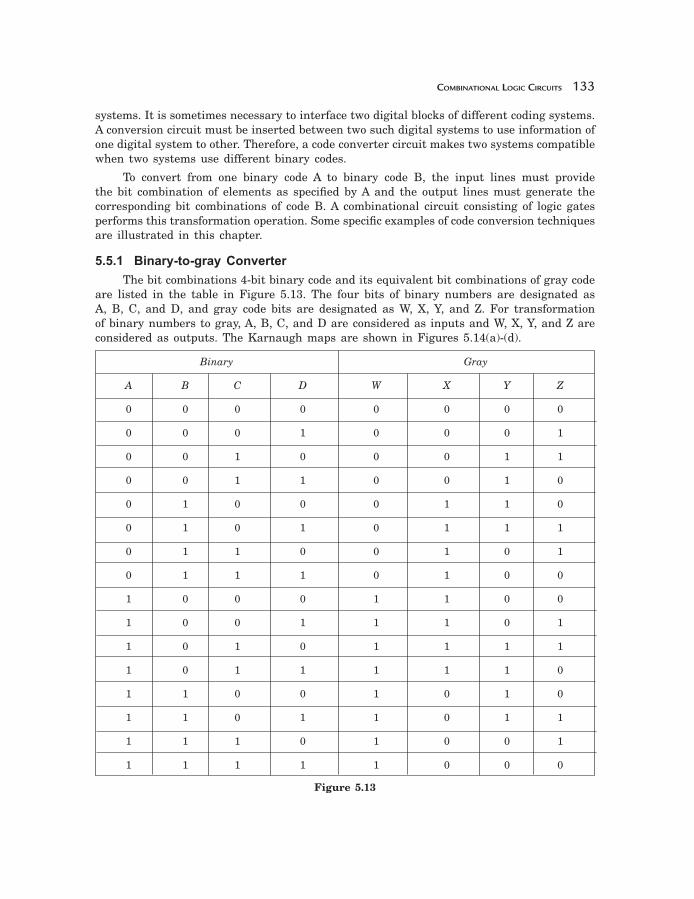
The bit combinations 4-bit binary code and its equivalent bit combinations of gray code are listed in the table in Figure 5.13. The four bits of binary numbers are designated as A, B, C, and D, and gray code bits are designated as W, X, Y, and Z. For transformation of binary numbers to gray, A, B, C, and D are considered as inputs and W, X, Y, and Z are considered as outputs. The Karnaugh maps are shown in Figures 5.14(a)-(d).
Binary Gray
A B C D W X Y Z
0 0 0 0 0 0 0 0
0 0 0 1 0 0 0 1
0 0 1 0 0 0 1 1
0 0 1 1 0 0 1 0
0 1 0 0 0 1 1 0
0 1 0 1 0 1 1 1
0 1 1 0 0 1 0 1
0 1 1 1 0 1 0 0
1 0 0 0 1 1 0 0
1 0 0 1 1 1 0 1
1 0 1 0 1 1 1 1
1 0 1 1 1 1 1 0
1 1 0 0 1 0 1 0
1 1 0 1 1 0 1 1
1 1 1 0 1 0 0 1
1 1 1 1 1 0 0 0
Figure 5.13

134 DIGITAL PRINCIPLES AND LOGIC DESIGN
C′D′ C′D CD CD′ C′D′ C′D CD CD′
A′B′ A′B′
A′B A′B 1 1 1 1
AB 1 1 1 1 AB
AB′ 1 1 1 1 AB′ 1 1 1 1
Figure 5.14(a) Karnaugh map for W. Figure 5.14(b) Karnaugh map for X.
C′D′ C′D CD CD′ C′D′ C′D CD CD′
A′B′ 1 1 A′B′ 1 1
A′B 1 1 A′B 1 1
AB 1 1 AB 1 1
AB′ 1 1 AB′ 1 1 Figure 5.14(c) Karnaugh map for Y. Figure 5.14(d) Karnaugh map for Z.
From the Karnaugh maps of Figure 5.14, we get
W = A, X = A′B + AB′ = A⊕B,
Y = BC′ + B′C = B⊕C, and Z = C′D + CD′= C⊕D.
Figure 5.15
Figure 5.15 demonstrates the circuit diagram with logic gates.
COMBINATIONAL LOGIC CIRCUITS 135
5.5.2 Gray-to-binary Converter
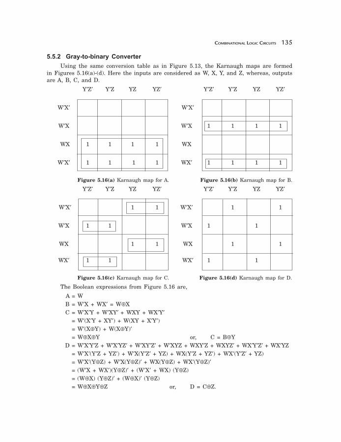
Using the same conversion table as in Figure 5.13, the Karnaugh maps are formed in Figures 5.16(a)-(d). Here the inputs are considered as W, X, Y, and Z, whereas, outputs are A, B, C, and D.
Y′Z′ Y′Z YZ YZ′ Y′Z′ Y′Z YZ YZ′
W′X′ W′X′
W′X W′X 1 1 1 1
WX 1 1 1 1 WX
W′X′ 1 1 1 1 WX′ 1 1 1 1
Figure 5.16(a) Karnaugh map for A. Figure 5.16(b) Karnaugh map for B.
Y′Z′ Y′Z YZ YZ′ Y′Z′ Y′Z YZ YZ′
W′X′ 1 1 W′X′ 1 1
W′X 1 1 W′X 1 1
WX 1 1 WX 1 1
WX′ 1 1 WX′ 1 1
Figure 5.16(c) Karnaugh map for C. Figure 5.16(d) Karnaugh map for D.
The Boolean expressions from Figure 5.16 are,
A = W B = W′X + WX′ = W⊕X C = W′X′Y + W′XY′ + WXY + WX′Y′ = W′(X′Y + XY′) + W(XY + X′Y′) = W′(X⊕Y) + W(X⊕Y)′ = W⊕X⊕Y or, C = B⊕Y D = W′X′Y′Z + W′X′YZ′ + W′XY′Z′ + W′XYZ + WXY′Z + WXYZ′ + WX′Y′Z′ + WX′YZ = W′X′(Y′Z + YZ′) + W′X(Y′Z′ + YZ) + WX(Y′Z + YZ′) + WX′(Y′Z′ + YZ) = W′X′(Y⊕Z) + W′X(Y⊕Z)′ + WX(Y⊕Z) + WX′(Y⊕Z)′ = (W′X + WX′)(Y⊕Z)′ + (W′X′ + WX) (Y⊕Z) = (W⊕X) (Y⊕Z)′ + (W⊕X)′ (Y⊕Z) = W⊕X⊕Y⊕Z or, D = C⊕Z.

136 DIGITAL PRINCIPLES AND LOGIC DESIGN
From the Boolean expressions above, the circuit diagram of a gray-to-binary code converter is shown in Figure 5.17.
Figure 5.17
It may be noticed that a binary-to-gray converter and a gray-to-binary converter as illustrated above are four bits. However, these codes are not limited to four bits only. By similar process both the binary-to-gray and gray-to-binary code converter can be developed for a higher number of bits.
5.5.3 BCD-to-excess-3 Code Converter
The bit combinations of both the BCD (Binary Coded Decimal) and Excess-3 codes represent decimal digits from 0 to 9. Therefore each of the code systems contains four bits and so there must be four input variables and four output variables. Figure 5.18 provides the list of the bit combinations or truth table and equivalent decimal values. The symbols A, B, C, and D are designated as the bits of the BCD system, and W, X, Y, and Z are designated as the bits of the Excess-3 code system. It may be noted that though 16 combinations are possible from four bits, both code systems use only 10 combinations. The rest of the bit combinations never occur and are treated as don’t-care conditions.
Decimal BCD code Excess-3 code
Equivalent A B C D W X Y Z
0 0 0 0 0 0 0 1 1
1 0 0 0 1 0 1 0 0
2 0 0 1 0 0 1 0 1
3 0 0 1 1 0 1 1 0
4 0 1 0 0 0 1 1 1
5 0 1 0 1 1 0 0 0
6 0 1 1 0 1 0 0 1
7 0 1 1 1 1 0 1 0
8 1 0 0 0 1 0 1 1
9 1 0 0 1 1 1 0 0
Figure 5.18
W Y
B DC
X Z
A
COMBINATIONAL LOGIC CIRCUITS 137
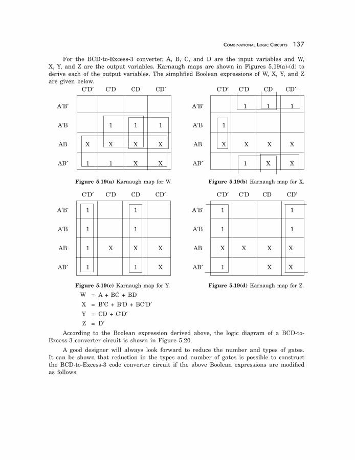
For the BCD-to-Excess-3 converter, A, B, C, and D are the input variables and W, X, Y, and Z are the output variables. Karnaugh maps are shown in Figures 5.19(a)-(d) to derive each of the output variables. The simplifi ed Boolean expressions of W, X, Y, and Z are given below. C′D′ C′D CD CD’ C′D′ C′D CD CD′
A′B′ A′B′ 1 1 1
A′B 1 1 1 A′B 1
AB X X X X AB X X X X
AB′ 1 1 X X AB′ 1 X X
Figure 5.19(a) Karnaugh map for W. Figure 5.19(b) Karnaugh map for X.
C′D′ C′D CD CD′ C′D′ C′D CD CD′
A′B′ 1 1 A′B′ 1 1
A′B 1 1 A′B 1 1
AB 1 X X X AB X X X X
AB′ 1 1 X AB′ 1 X X
Figure 5.19(c) Karnaugh map for Y. Figure 5.19(d) Karnaugh map for Z.
W = A + BC + BD
X = B′C + B′D + BC′D′ Y = CD + C′D′ Z = D′According to the Boolean expression derived above, the logic diagram of a BCD-to-
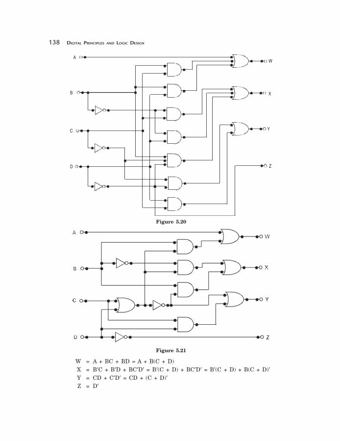
Excess-3 converter circuit is shown in Figure 5.20.
A good designer will always look forward to reduce the number and types of gates. It can be shown that reduction in the types and number of gates is possible to construct the BCD-to-Excess-3 code converter circuit if the above Boolean expressions are modifi ed as follows.
138 DIGITAL PRINCIPLES AND LOGIC DESIGN
Figure 5.20
Figure 5.21
W = A + BC + BD = A + B(C + D) X = B′C + B′D + BC′D′ = B′(C + D) + BC′D′ = B′(C + D) + B(C + D)′ Y = CD + C′D′ = CD + (C + D)′ Z = D′
XB
C
D
Y
Z
WA
COMBINATIONAL LOGIC CIRCUITS 139
The BCD-to-Excess-3 converter circuit has been redrawn in Figure 5.21 according to the modifi ed Boolean expressions above. Here, three-input AND gates and three-input OR gates are totally removed and the required number of gates has been reduced.
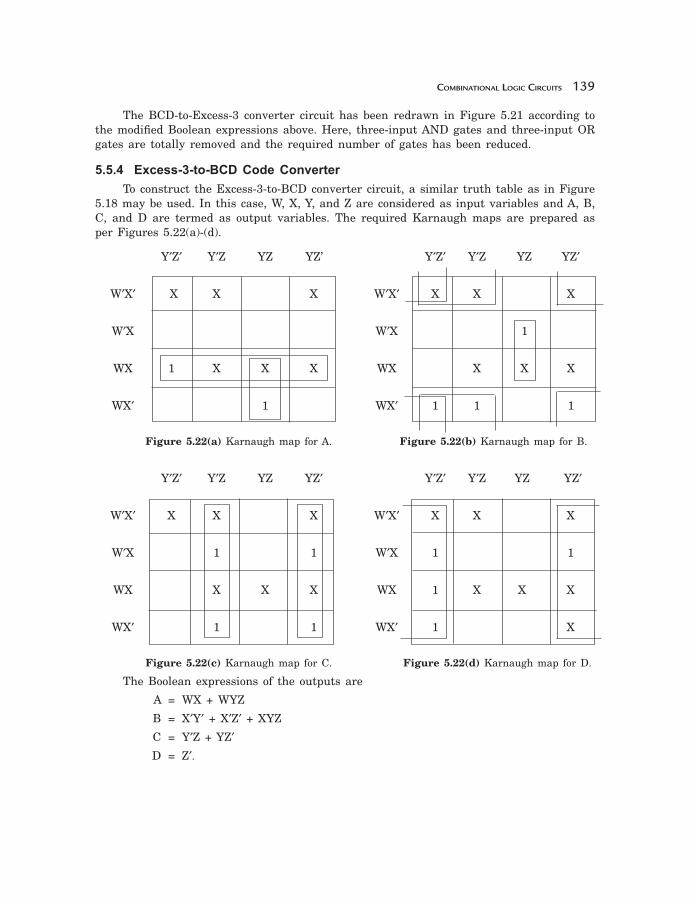
5.5.4 Excess-3-to-BCD Code Converter
To construct the Excess-3-to-BCD converter circuit, a similar truth table as in Figure 5.18 may be used. In this case, W, X, Y, and Z are considered as input variables and A, B, C, and D are termed as output variables. The required Karnaugh maps are prepared as per Figures 5.22(a)-(d).
Y′Z′ Y′Z YZ YZ’ Y′Z′ Y′Z YZ YZ′
W′X′ X X X W′X′ X X X
W′X W′X 1
WX 1 X X X WX X X X
WX′ 1 WX′ 1 1 1
Figure 5.22(a) Karnaugh map for A. Figure 5.22(b) Karnaugh map for B.
Y′Z′ Y′Z YZ YZ′ Y′Z′ Y′Z YZ YZ′
W′X′ X X X W′X′ X X X
W′X 1 1 W′X 1 1
WX X X X WX 1 X X X
WX′ 1 1 WX′ 1 X
Figure 5.22(c) Karnaugh map for C. Figure 5.22(d) Karnaugh map for D.
The Boolean expressions of the outputs are
A = WX + WYZ
B = X′Y′ + X′Z′ + XYZ
C = Y′Z + YZ′ D = Z′.

140 DIGITAL PRINCIPLES AND LOGIC DESIGN
Figure 5.23
The logic diagram of an Excess-3-to-BCD converter is shown in Figure 5.23.
The alternative circuit diagram of Figure 5.24 can be made after the following modifi cation on the above Boolean expressions.
A = WX + WYZ = W(X + YZ)
B = X′Y′ + X′Z′ + XYZ = X′(Y′ + Z′) + XYZ = X′(YZ)′ + XYZ
C = Y′Z + YZ′ D = Z′
Figure 5.24

COMBINATIONAL LOGIC CIRCUITS 141
5.6 PARITY GENERATOR AND CHECKER
Parity is a very useful tool in information processing in digital computers to indicate any presence of error in bit information. External noise and loss of signal strength cause loss of data bit information while transporting data from one device to other device, located inside the computer or externally. To indicate any occurrence of error, an extra bit is included with the message according to the total number of 1s in a set of data, which is called parity. If the extra bit is considered 0 if the total number of 1s is even and 1 for odd quantities of 1s in a set of data, then it is called even parity. On the other hand, if the extra bit is 1 for even quantities of 1s and 0 for an odd number of 1s, then it is called odd parity.
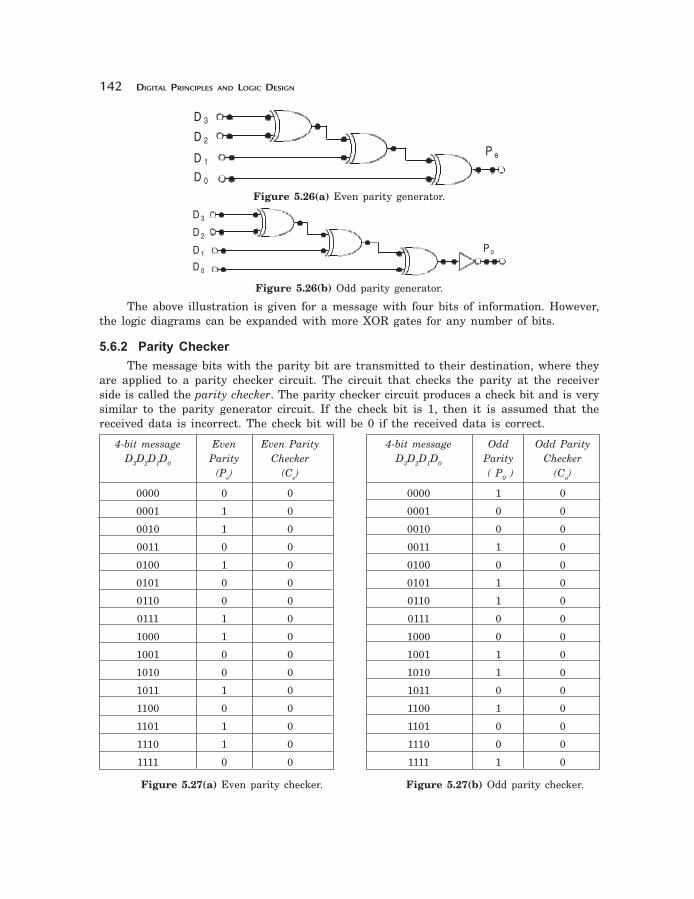
5.6.1 Parity Generator
A parity generator is a combination logic system to generate the parity bit at the transmitting side. A table in Figure 5.25 illustrates even parity as well as odd parity for a message consisting of four bits.
Four bit Message Even Parity Odd Parity D3D2D1D0 ( P e ) ( Po )
0000 0 1
0001 1 0
0010 1 0
0011 0 1
0100 1 0
0101 0 1
0110 0 1
0111 1 0
1000 1 0
1001 0 1
1010 0 1
1011 1 0
1100 0 1
1101 1 0
1110 1 0
1111 0 1
Figure 5.25
If the message bit combination is designated as D3D2D1D0, and Pe , Po are the even and odd parity respectively, then it is obvious from the table that the Boolean expressions of even parity and odd parity are
Pe = D3⊕D2⊕D1⊕D0 and Po = (D 3⊕D2⊕D1⊕D0)′. These can be confi rmed by Karnaugh maps, also (not shown here). The logic diagrams
are shown in Figures 5.26(a)-(b).
142 DIGITAL PRINCIPLES AND LOGIC DESIGN
Figure 5.26(a) Even parity generator.
Figure 5.26(b) Odd parity generator.
The above illustration is given for a message with four bits of information. However, the logic diagrams can be expanded with more XOR gates for any number of bits.
5.6.2 Parity Checker
The message bits with the parity bit are transmitted to their destination, where they are applied to a parity checker circuit. The circuit that checks the parity at the receiver side is called the parity checker. The parity checker circuit produces a check bit and is very similar to the parity generator circuit. If the check bit is 1, then it is assumed that the received data is incorrect. The check bit will be 0 if the received data is correct.
4-bit message Even Even Parity 4-bit message Odd Odd Parity D3D2D1D0 Parity Checker D3D2D1D0 Parity Checker (P e) (Ce) ( P0 ) (Co)
0000 0 0 0000 1 0
0001 1 0 0001 0 0
0010 1 0 0010 0 0
0011 0 0 0011 1 0
0100 1 0 0100 0 0
0101 0 0 0101 1 0
0110 0 0 0110 1 0
0111 1 0 0111 0 0
1000 1 0 1000 0 0
1001 0 0 1001 1 0
1010 0 0 1010 1 0
1011 1 0 1011 0 0
1100 0 0 1100 1 0
1101 1 0 1101 0 0
1110 1 0 1110 0 0
1111 0 0 1111 1 0
Figure 5.27(a) Even parity checker. Figure 5.27(b) Odd parity checker.
D 3
D 2
D 1
D 0
P e
D 3
D 2
D 1
D 0
P o

COMBINATIONAL LOGIC CIRCUITS 143
The tables in Figures 5.27(a)-(b) demonstrate the above. Note that the check bit is 0 for all the bit combinations of correct data. For incorrect data the parity check bit will be another logic value. Parity checker circuits are the same as parity generator circuits as shown in Figures 5.28(a)-(b).
Figure 5.28(a) Even parity checker.
Figure 5.28(b) Odd parity checker.
5.7 SOME EXAMPLES OF COMBINATIONAL LOGIC CIRCUITS
Example 5.1. Find the squares of 3-bit numbers.
Solution. With three bits a maximum of eight combinations are possible with decimal equivalents of 0 to 7. By squaring of the decimal numbers the maximum decimal number produced is 49, which can be formed with six bits. Let us consider three input variables are X, Y, and Z, and six output variables are A, B, C, D, E, and F. A truth table is prepared as in Figure 5.29 and Karnaugh maps for each of the output variables are shown in Figures 5.30(a)-(f).
Input variables Output variables
Decimal X Y Z Decimal A B C D E F Equivalent Equivalent
0 0 0 0 0 0 0 0 0 0 0
1 0 0 1 1 0 0 0 0 0 1
2 0 1 0 4 0 0 0 1 0 0
3 0 1 1 9 0 0 1 0 0 1
4 1 0 0 16 0 1 0 0 0 0
5 1 0 1 25 0 1 1 0 0 1
6 1 1 0 36 1 0 0 1 0 0
7 1 1 1 49 1 1 0 0 0 1
Figure 5.29
D 3
D 2
D 1
D 0
P e
C e
D3
D2
D1
D0
Po
Co

144 DIGITAL PRINCIPLES AND LOGIC DESIGN
Y′Z′ Y′Z YZ YZ′ Y′Z′ Y′Z YZ YZ′
X′ X′
X 1 1 X 1 1 1
Figure 5.30(a) Karnaugh map for A. Figure 5.30(b) Karnaugh map for B.
Y′Z′ Y′Z YZ YZ′ Y′Z′ Y′Z YZ YZ′
X′ 1 X′ 1
X 1 X 1
Figure 5.30(c) Karnaugh map for C. Figure 5.30(d) Karnaugh map for D.
Y′Z′ Y′Z YZ YZ’′ Y′Z′ Y′Z YZ YZ′
X′ 0 0 0 0 X′ 1 1
X 0 0 0 0 X 1 1
Figure 5.30(e) Karnaugh map for E. Figure 5.30(f) Karnaugh map for F.
Figure 5.31
X A
B
C
D
E
F
Y
Z
COMBINATIONAL LOGIC CIRCUITS 145
The Boolean expressions of the output variables are
A = XY B = XY′ + XZ
C = X′YZ + XY′Z = (X′Y + XY′)Z D = YZ′ E = 0 and F = Z.
The circuit diagram of the combinational network to obtain squares of three-bit numbers is shown in Figure 5.31.
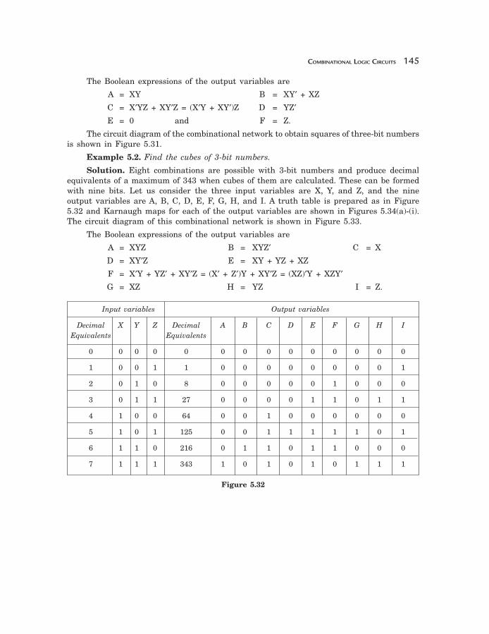
Example 5.2. Find the cubes of 3-bit numbers.
Solution. Eight combinations are possible with 3-bit numbers and produce decimal equivalents of a maximum of 343 when cubes of them are calculated. These can be formed with nine bits. Let us consider the three input variables are X, Y, and Z, and the nine output variables are A, B, C, D, E, F, G, H, and I. A truth table is prepared as in Figure 5.32 and Karnaugh maps for each of the output variables are shown in Figures 5.34(a)-(i). The circuit diagram of this combinational network is shown in Figure 5.33.
The Boolean expressions of the output variables are
A = XYZ B = XYZ′ C = X
D = XY′Z E = XY + YZ + XZ
F = X′Y + YZ′ + XY′Z = (X′ + Z′)Y + XY′Z = (XZ)′Y + XZY′ G = XZ H = YZ I = Z.
Input variables Output variables
Decimal X Y Z Decimal A B C D E F G H I Equivalents Equivalents
0 0 0 0 0 0 0 0 0 0 0 0 0 0
1 0 0 1 1 0 0 0 0 0 0 0 0 1
2 0 1 0 8 0 0 0 0 0 1 0 0 0
3 0 1 1 27 0 0 0 0 1 1 0 1 1
4 1 0 0 64 0 0 1 0 0 0 0 0 0
5 1 0 1 125 0 0 1 1 1 1 1 0 1
6 1 1 0 216 0 1 1 0 1 1 0 0 0
7 1 1 1 343 1 0 1 0 1 0 1 1 1
Figure 5.32

146 DIGITAL PRINCIPLES AND LOGIC DESIGN
Figure 5.33
Y′Z′ Y′Z YZ YZ′ Y′Z′ Y′Z YZ YZ′
X′ X′
X 1 X 1
Figure 5.34(a) Karnaugh map for A. Figure5.34(b) Karnaugh map for B.
Y′Z′ Y′Z YZ YZ′ Y′Z′ Y′Z YZ YZ′
X′ X′
X 1 1 1 1 X 1
Figure 5.34(c) Karnaugh map for C. Figure 5.34(d) Karnaugh map for D.
Y′Z′ Y′Z YZ YZ′ Y′Z′ Y′Z YZ YZ′
X′ 1 X′ 1 1
X 1 1 1 X 1 1
Figure 5.34(e) Karnaugh map for E. Figure 5.34(f) Karnaugh map for F.
COMBINATIONAL LOGIC CIRCUITS 147
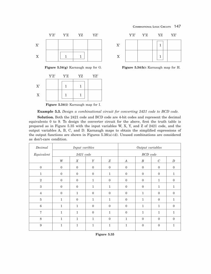
Y′Z′ Y′Z YZ YZ′ Y′Z′ Y′Z YZ YZ′
X′ X′ 1
X 1 1 X 1
Figure 5.34(g) Karnaugh map for G. Figure 5.34(h): Karnaugh map for H.
Y′Z′ Y′Z YZ YZ′
X′ 1 1 X 1 1 Figure 5.34(i) Karnaugh map for I.
Example 5.3. Design a combinational circuit for converting 2421 code to BCD code.
Solution. Both the 2421 code and BCD code are 4-bit codes and represent the decimal equivalents 0 to 9. To design the converter circuit for the above, fi rst the truth table is prepared as in Figure 5.35 with the input variables W, X, Y, and Z of 2421 code, and the output variables A, B, C, and D. Karnaugh maps to obtain the simplifi ed expressions of the output functions are shown in Figures 5.36(a)-(d). Unused combinations are considered as don’t-care condition.
Decimal Input varibles Output variables
Equivalent 2421 code BCD code
W X Y Z A B C D
0 0 0 0 0 0 0 0 0
1 0 0 0 1 0 0 0 1
2 0 0 1 0 0 0 1 0
3 0 0 1 1 0 0 1 1
4 0 1 0 0 0 1 0 0
5 1 0 1 1 0 1 0 1
6 1 1 0 0 0 1 1 0
7 1 1 0 1 0 1 1 1
8 1 1 1 0 1 0 0 0
9 1 1 1 1 1 0 0 1
Figure 5.35
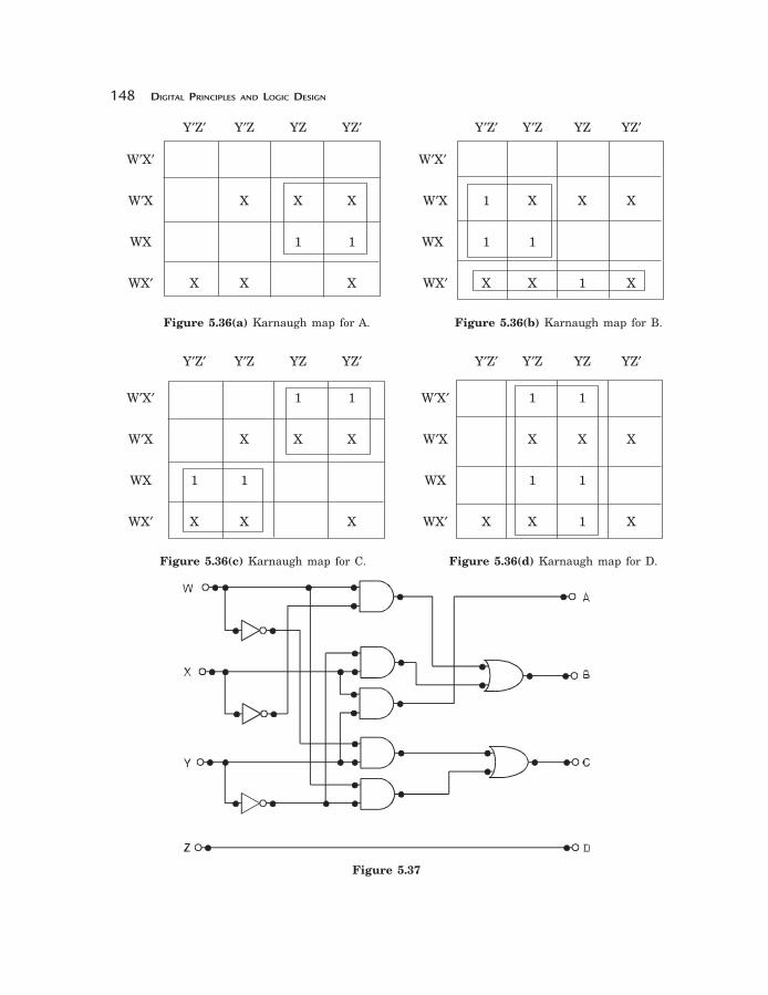
148 DIGITAL PRINCIPLES AND LOGIC DESIGN
Y′Z′ Y′Z YZ YZ′ Y′Z′ Y′Z YZ YZ′
W′X′ W′X′
W′X X X X W′X 1 X X X
WX 1 1 WX 1 1
WX′ X X X WX′ X X 1 X
Figure 5.36(a) Karnaugh map for A. Figure 5.36(b) Karnaugh map for B.
Y′Z′ Y′Z YZ YZ′ Y′Z′ Y′Z YZ YZ′
W′X′ 1 1 W′X′ 1 1
W′X X X X W′X X X X
WX 1 1 WX 1 1
WX′ X X X WX′ X X 1 X
Figure 5.36(c) Karnaugh map for C. Figure 5.36(d) Karnaugh map for D.
Figure 5.37

COMBINATIONAL LOGIC CIRCUITS 149
The Boolean expressions for the output functions are
A = XY B = XY′+WX′C = W′Y + WY′ D = Z.
The logic diagram of the required converter is shown in Figure 5.37.
Example 5.4. Design a combinational circuit that converts 2421 code to 84-2-1 code, and also the converter circuit for 84-2-1 code to 2421 code.
Solution. Both the codes represent binary codes for decimal digits 0 to 9. Let A, B, C, and D be represented as 2421 code variables and W, X, Y, and Z be variables for 84-2-1. The truth table is shown in Figure 5.38. The Karnaugh maps for W, X, Y, and Z in respect to A, B, C, and D are shown in Figure 5.39(a)-(d).
Decimal 2421 Code 84-2-1 code
Digits A B C D W X Y Z
0 0 0 0 0 0 0 0 0
1 0 0 0 1 0 1 1 1
2 0 0 1 0 0 1 1 0
3 0 0 1 1 0 1 0 1
4 0 1 0 0 0 1 0 0
5 1 0 1 1 1 0 1 1
6 1 1 0 0 1 0 1 0
7 1 1 0 1 1 0 0 1
8 1 1 1 0 1 0 0 0
9 1 1 1 1 1 1 1 1
Figure 5.38
C′D′ C′D CD CD′ C′D′ C′D CD CD′
A′B′ A′B′ 1 1 1
A′B X X X A′B 1 X X X
AB 1 1 1 1 AB 1
AB′ X X 1 X AB′ X X X
Figure 5.39(a) Karnaugh map for W. Figure 5.39(b) Karnaugh map for X.
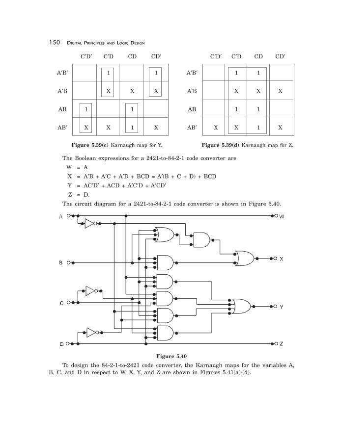
150 DIGITAL PRINCIPLES AND LOGIC DESIGN
C′D′ C′D CD CD′ C′D′ C′D CD CD′
A′B′ 1 1 A′B′ 1 1
A′B X X X A′B X X X
AB 1 1 AB 1 1
AB′ X X 1 X AB′ X X 1 X
Figure 5.39(c) Karnaugh map for Y. Figure 5.39(d) Karnaugh map for Z.
The Boolean expressions for a 2421-to-84-2-1 code converter are
W = A
X = A′B + A′C + A′D + BCD = A′(B + C + D) + BCD
Y = AC′D′ + ACD + A′C′D + A′CD′ Z = D.
The circuit diagram for a 2421-to-84-2-1 code converter is shown in Figure 5.40.
Figure 5.40
To design the 84-2-1-to-2421 code converter, the Karnaugh maps for the variables A, B, C, and D in respect to W, X, Y, and Z are shown in Figures 5.41(a)-(d).
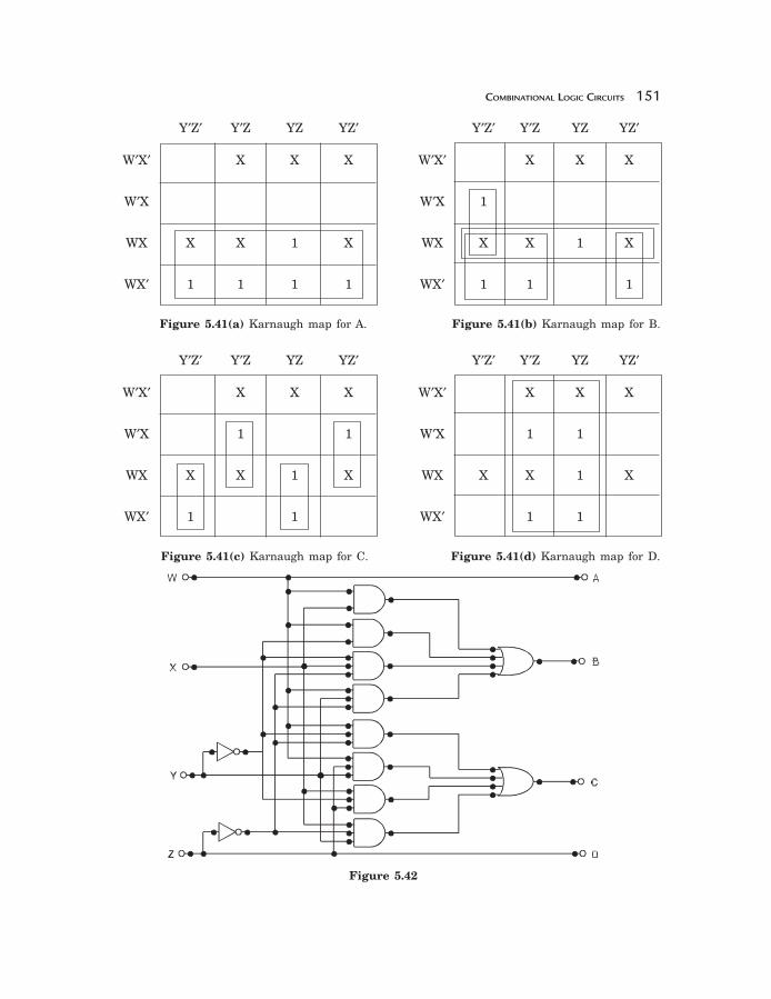
COMBINATIONAL LOGIC CIRCUITS 151
Y′Z′ Y′Z YZ YZ′ Y′Z′ Y′Z YZ YZ′
W′X′ X X X W′X′ X X X
W′X W′X 1
WX X X 1 X WX X X 1 X
WX′ 1 1 1 1 WX′ 1 1 1
Figure 5.41(a) Karnaugh map for A. Figure 5.41(b) Karnaugh map for B.
Y′Z′ Y′Z YZ YZ′ Y′Z′ Y′Z YZ YZ′
W′X′ X X X W′X′ X X X
W′X 1 1 W′X 1 1
WX X X 1 X WX X X 1 X
WX′ 1 1 WX′ 1 1
Figure 5.41(c) Karnaugh map for C. Figure 5.41(d) Karnaugh map for D.
Figure 5.42
152 DIGITAL PRINCIPLES AND LOGIC DESIGN
The Boolean expressions for an 84-2-1-to-2421 code converter are
A = W
B = WX + WY′ + XY′Z′ + WYZ′ C = WY′Z′ + WYZ + XY′Z + XYZ′ D = Z.
The combinational circuit for an 84-2-1-to-2421 code converter is shown in Figure 5.42.
Example 5.5. Design a combinational circuit for a BCD-to-seven-segment decoder.
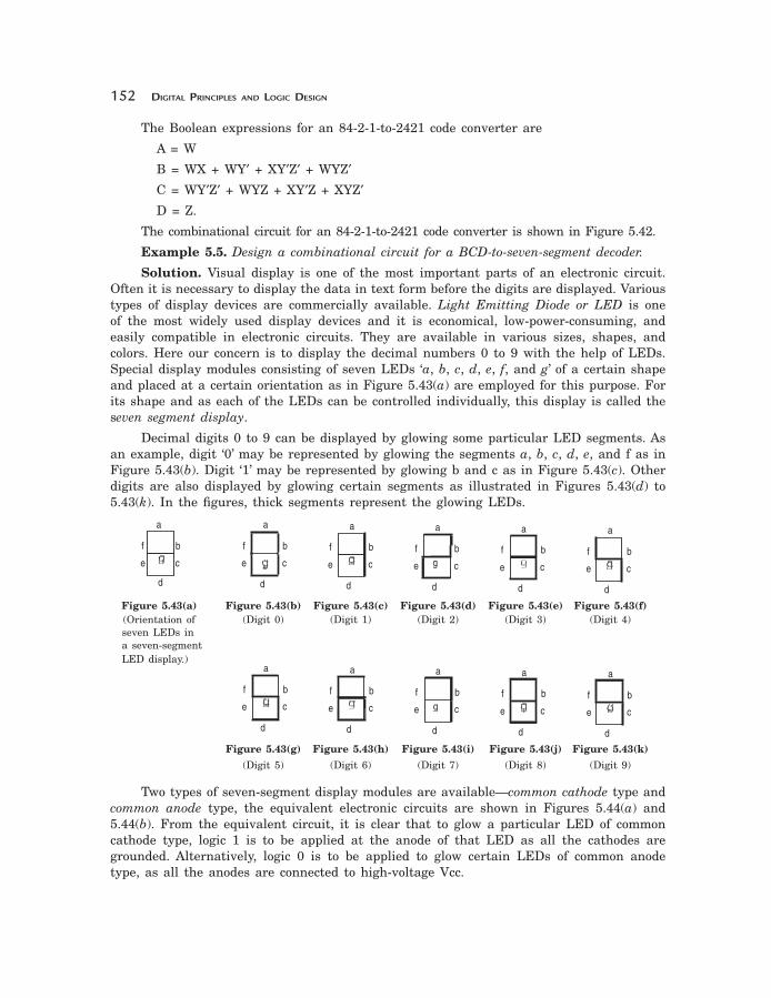
Solution. Visual display is one of the most important parts of an electronic circuit. Often it is necessary to display the data in text form before the digits are displayed. Various types of display devices are commercially available. Light Emitting Diode or LED is one of the most widely used display devices and it is economical, low-power-consuming, and easily compatible in electronic circuits. They are available in various sizes, shapes, and colors. Here our concern is to display the decimal numbers 0 to 9 with the help of LEDs. Special display modules consisting of seven LEDs ‘a, b, c, d, e, f, and g’ of a certain shape and placed at a certain orientation as in Figure 5.43(a) are employed for this purpose. For its shape and as each of the LEDs can be controlled individually, this display is called the seven segment display.
Decimal digits 0 to 9 can be displayed by glowing some particular LED segments. As an example, digit ‘0’ may be represented by glowing the segments a, b, c, d, e, and f as in Figure 5.43(b). Digit ‘1’ may be represented by glowing b and c as in Figure 5.43(c). Other digits are also displayed by glowing certain segments as illustrated in Figures 5.43(d) to 5.43(k). In the fi gures, thick segments represent the glowing LEDs.
Figure 5.43(a) Figure 5.43(b) Figure 5.43(c) Figure 5.43(d) Figure 5.43(e) Figure 5.43(f) (Orientation of (Digit 0) (Digit 1) (Digit 2) (Digit 3) (Digit 4) seven LEDs in a seven-segment LED display.)
Figure 5.43(g) Figure 5.43(h) Figure 5.43(i) Figure 5.43(j) Figure 5.43(k)
(Digit 5) (Digit 6) (Digit 7) (Digit 8) (Digit 9)
Two types of seven-segment display modules are available—common cathode type and common anode type, the equivalent electronic circuits are shown in Figures 5.44(a) and 5.44(b). From the equivalent circuit, it is clear that to glow a particular LED of common cathode type, logic 1 is to be applied at the anode of that LED as all the cathodes are grounded. Alternatively, logic 0 is to be applied to glow certain LEDs of common anode type, as all the anodes are connected to high-voltage Vcc.
a a a a a a
f f f f f fe e e e g e e
d d d d d d
c c c c c c
b b b b b b
a a a a a
f f f f fe e e g e e
d d d d d
c c c c c
b b b b b

COMBINATIONAL LOGIC CIRCUITS 153
Figure 5.44(a) Common cathode LED. Figure 5.44(b) Common anode LED.
Decimal Input Variables Output Variables as Seven Segment Display
Numbers A B C D a b c d e f g
0 0 0 0 0 1 1 1 1 1 1 0
1 0 0 0 1 0 1 1 0 0 0 0
2 0 0 1 0 1 1 0 1 1 0 1
3 0 0 1 1 1 1 1 1 0 0 1
4 0 1 0 0 0 1 1 0 0 1 1
5 0 1 0 1 1 0 1 1 0 1 1
6 0 1 1 0 0 0 1 1 1 1 1
7 0 1 1 1 1 1 1 0 0 0 0
8 1 0 0 0 1 1 1 1 1 1 1
9 1 0 0 1 1 1 1 0 0 1 1
Figure 5.45 (For a common cathode display.)
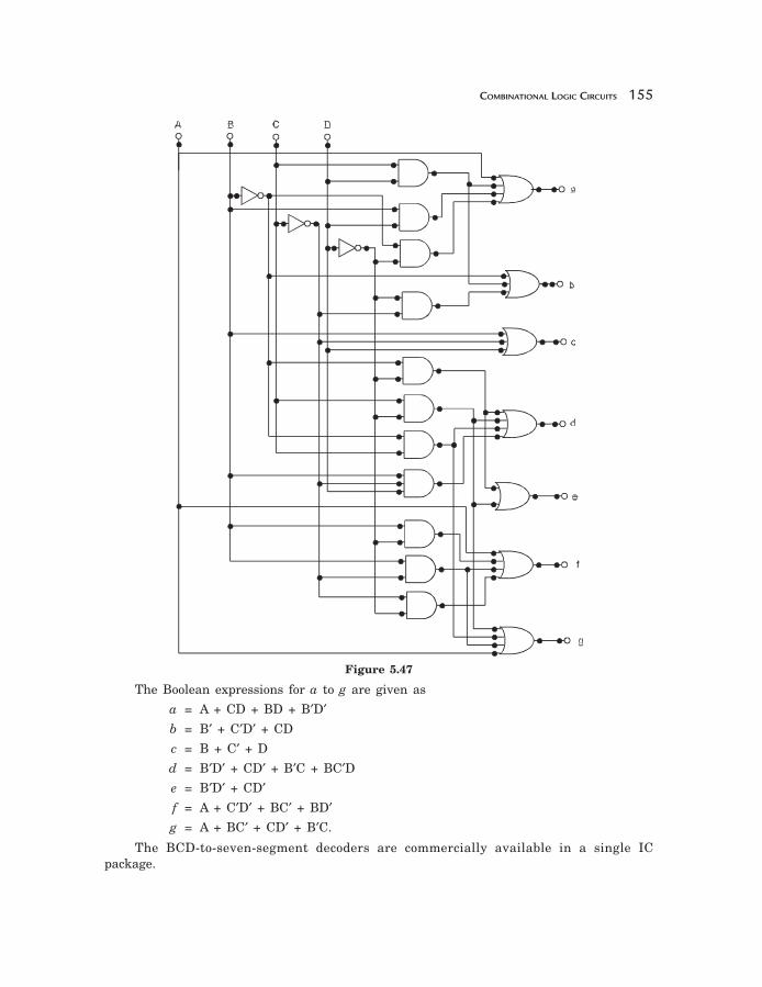
Every decimal digit of 0 to 9 is represented by the BCD data, consisting of four input variables A, B, C, and D. A truth table can be made for each of the LED segments. A truth table for a common cathode display is shown in Figure 5.45. The Boolean expression for output variables a to g are obtained with the help of the Karnaugh maps as shown in Figures 5.46(a) to 5.46(g). The circuit diagram is developed as shown in Figure 5.47.
Note that the Boolean expressions of the outputs of a common anode type display are the complemented form of the respective outputs of a common cathode type.
C′D′ C′D CD CD′ C′D′ C′D CD CD′
A′B′ 1 1 1 A′B′ 1 1 1 1
A′B 1 1 A′B 1 1
AB X X X X AB X X X X
AB′ 1 1 X X AB′ 1 1 X X
Figure 5.46(a) Karnaugh map for a. Figure 5.46(b) Karnaugh map for b.
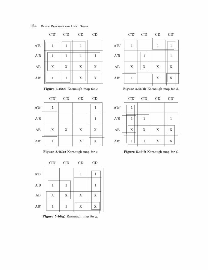
154 DIGITAL PRINCIPLES AND LOGIC DESIGN
C′D′ C′D CD CD′ C′D′ C′D CD CD′
A′B′ 1 1 1 A′B′ 1 1 1
A′B 1 1 1 1 A′B 1 1
AB X X X X AB X X X X
AB′ 1 1 X X AB′ 1 X X
Figure 5.46(c) Karnaugh map for c. Figure 5.46(d) Karnaugh map for d.
C′D′ C′D CD CD′ C′D′ C′D CD CD′
A′B′ 1 1 A′B′ 1
A′B 1 A′B 1 1 1
AB X X X X AB X X X X
AB′ 1 X X AB′ 1 1 X X
Figure 5.46(e) Karnaugh map for e. Figure 5.46(f) Karnaugh map for f.
C′D′ C′D CD CD′
A′B′ 1 1
A′B 1 1 1
AB X X X X
AB′ 1 1 X X
Figure 5.46(g) Karnaugh map for g.
COMBINATIONAL LOGIC CIRCUITS 155
Figure 5.47
The Boolean expressions for a to g are given as
a = A + CD + BD + B′D′b = B′ + C′D′ + CD
c = B + C′ + D
d = B′D′ + CD′ + B′C + BC′De = B′D′ + CD′f = A + C′D′ + BC′ + BD′g = A + BC′ + CD′ + B′C.
The BCD-to-seven-segment decoders are commercially available in a single IC package.

156 DIGITAL PRINCIPLES AND LOGIC DESIGN
5.8 COMBINATIONAL LOGIC WITH MSI AND LSI
The purpose of simplifi cation of Boolean functions is to obtain an algebraic expression with less number of literals and less numbers of logic gates. This results in low-cost circuit implementation. The design procedure for combinational circuits as described in the preceding sections is intended to minimize the number of logic gates to implement a given function. This classical procedure realizes the logic circuit with fewer gates with the assumption that the circuit with fewer gates will cost less. However, in practical design, with the arrival of a variety of integrated circuits (IC), this concept is always true.
Since one single IC package contains several number of logic gates, it is economical to use as many of the gates from an already used package, even if the total number of gates is increased by doing so. Moreover, some of the interconnections among the gates in many ICs are internal to the chip and it is more economical to use such types of ICs to minimize the external interconnections or wirings among the IC pins as much as possible. A typical example of this is if the circuit diagrams of Figures 5.23 and 5.24 are considered. Both circuit diagrams perform the function of Excess-3-to-BCD code conversion and consist of 13 logic gates. However, the circuit of Figure 5.23 needs six ICs (one 3-input OR, one 3-input AND, two 2-input AND, one 2-input OR, and one INVERTER, since one 3-input OR IC package contains three gates, one 3-input AND IC contains three gates, one 2-input AND IC contains four gates, one 2-input OR IC contains four gates, and one INVERTER IC contains six gates), but the circuit diagram of Figure 5.24 requires four ICs (two 2-input AND IC, one 2-input OR IC, and one INVERTER). So obviously, logic implementation of Figure 5.24 is economical because of its fewer number of IC packages. So for design with integrated circuits, it is not the count of logic gates that reduces the cost, but the number and type of IC packages used and the number of interconnections required to implement certain functions.
Though the classical method constitutes a general procedure, is very easy to understand, and certain to produce a result, on numerous occasions it does not achieve the best possible combinational circuit for a given function. Moreover, the truth table and simplifi cation procedure in this method become too cumbersome if the number of input variables is excessively large and the fi nal circuit obtained may require a relatively large number of ICs and interconnecting wires. In many cases the alternative design approach can lead to a far better combinational circuit for a given function with comparison to the classical method. The alternate design approach depends on the particular application and the ingenuity as well as experience of the designer. To handle a practical design problem, it should always be investigated which method is more suitable and effi cient.
Design approach of a combinational circuit is fi rst to analysis and to fi nd out whether the function is already available as an IC package. Numerous ICs are commercially available, some of which perform specifi c functions and are commonly employed in the design of digital computer system. If the required function is not exactly matched with any of the commercially available devices, a good designer will formulate a method to incorporate the ICs that are nearly suitable to the function.
A large number of integrated circuit packages are commercially available nowadays. They can be widely categorized into three groups—SSI or small scale integration where the number of logic gates is limited to ten in one IC package, MSI or medium scale integration where the number of logic gates is eleven to one hundred in one IC package, and LSI or large-scale integration containing more than one hundred gates in one package. Some of them are fabricated for specifi c functions. VLSI or very large scale integration IC packages

COMBINATIONAL LOGIC CIRCUITS 157
are also introduced, which perform dedicated functions achieving high circuit space reduction and interconnection reduction.
5.9 FOUR-BIT BINARY PARALLEL ADDER
In the preceding section, we discussed how two binary bits can be added and the addition of two binary bits with a carry. In practical situations it is required to add two data each containing more than one bit. Two binary numbers each of n bits can be added by means of a full adder circuit. Consider the example that two 4-bit binary numbers B4B3B2B1 and A4A3A2A1
are to be added with a carry input C1. This can be done by cascading four full adder circuits as shown in Figure 5.48. The least signifi cant bits A1, B1, and C1 are added to the produce sum output S1 and carry output C2. Carry output C2 is then added to the next signifi cant bits A2 and B2 producing sum output S2 and carry output C3. C3 is then added to A3 and B3
and so on. Thus fi nally producing the four-bit sum output S4S3S2S1 and fi nal carry output Cout. Such type of four-bit binary adder is commercially available in an IC package.
Figure 5.48
For the addition of two n bits of data, n numbers of full adders can be cascaded as demonstrated in Figure 5.48. It can be constructed with 4-bit, 2-bit, and 1-bit full adder IC packages. The carry output of one package must be connected to the carry input of the next higher order bit IC package of higher order bits.
The addition technique adopted here is a parallel type as all the bit addition operations are performed in parallel. Therefore, this type of adder is called a parallel adder. Serial types of adders are also available where a single full adder circuit can perform any n number of bit addition operations in association with shift registers and sequential logic network. This will be discussed in the later chapters.
The 4-bit parallel binary adder IC package is useful to develop combinational circuits. Some examples are demonstrated here.
Example 5.6. Design a BCD-to-Excess-3 code converter.
Figure 5.49
B4 B3 B 2 B1
S 4 S 3
C 3C 4 C 2 C 1
S 2 S1
FA FA FA FACout
A4 A3 A 2 A1
Excess-3 O utputs
Log ic 0
Log ic 0 Log ic 1
Not Used Cout
BCD Inputs
B4 A4B3 A3B2 A2B1 A1
C in4-BIT BINA RY ADDER
S4 S3 S2 S 1
158 DIGITAL PRINCIPLES AND LOGIC DESIGN
If we analyze the BCD code and Excess-3 code critically, you will see that Excess-3 codecan be achieved by adding 0011 (decimal equivalent is 3) with BCD numbers. So a 4-bit binary adder IC can solve this very easily as shown in Figure 5.49.
It may be noticed that a BCD-to-Excess-3 converter has been implemented by classical method in Section 5.5.3, where four OR gates, four AND gates, and three INVERTER gates are employed. In terms of IC packages, three SSI packages (one AND gates IC, one OR gate IC, and one INVERTER IC) are used and a good amount of interconnections are present. In comparison to that the circuit developed in Figure 5.49 requires only one MSI IC of 4-bit binary adder and interconnections have reduced drastically. So the combinational circuit of Figure 5.49 is of low cost, trouble-free, less board, space consuming and less power dissipation.
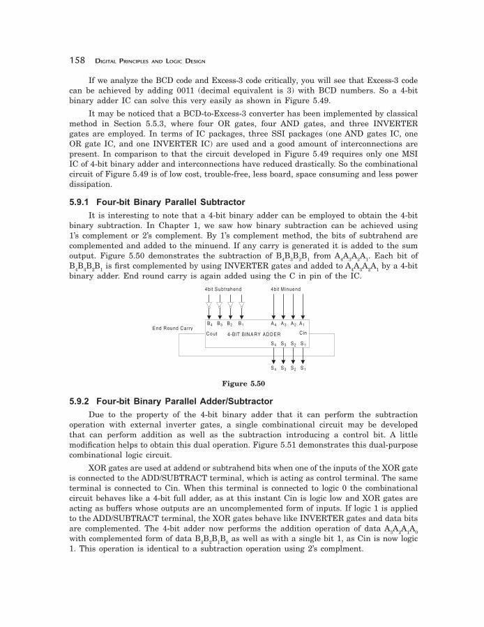
5.9.1 Four-bit Binary Parallel Subtractor
It is interesting to note that a 4-bit binary adder can be employed to obtain the 4-bit binary subtraction. In Chapter 1, we saw how binary subtraction can be achieved using 1’s complement or 2’s complement. By 1’s complement method, the bits of subtrahend are complemented and added to the minuend. If any carry is generated it is added to the sum output. Figure 5.50 demonstrates the subtraction of B4B3B2B1 from A4A3A2A1. Each bit of B4B3B2B1 is fi rst complemented by using INVERTER gates and added to A4A3A2A1 by a 4-bit binary adder. End round carry is again added using the C in pin of the IC.
Figure 5.50
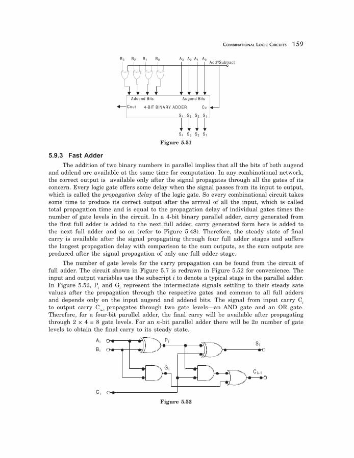
5.9.2 Four-bit Binary Parallel Adder/Subtractor
Due to the property of the 4-bit binary adder that it can perform the subtraction operation with external inverter gates, a single combinational circuit may be developed that can perform addition as well as the subtraction introducing a control bit. A little modifi cation helps to obtain this dual operation. Figure 5.51 demonstrates this dual-purpose combinational logic circuit.
XOR gates are used at addend or subtrahend bits when one of the inputs of the XOR gate is connected to the ADD/SUBTRACT terminal, which is acting as control terminal. The same terminal is connected to Cin. When this terminal is connected to logic 0 the combinational circuit behaves like a 4-bit full adder, as at this instant Cin is logic low and XOR gates are acting as buffers whose outputs are an uncomplemented form of inputs. If logic 1 is applied to the ADD/SUBTRACT terminal, the XOR gates behave like INVERTER gates and data bits are complemented. The 4-bit adder now performs the addition operation of data A3A2A1A0
with complemented form of data B3B2B1B0 as well as with a single bit 1, as Cin is now logic 1. This operation is identical to a subtraction operation using 2’s complment.
End Round CarryCout
4bit M inuend4bit Subtrahend
4-BIT BINA RY ADDER
B4 A 4B3 A 3B2 A 2B1 A 1
C in
S4 S3 S2 S 1
S4 S3 S2 S 1
COMBINATIONAL LOGIC CIRCUITS 159
Figure 5.51
5.9.3 Fast Adder
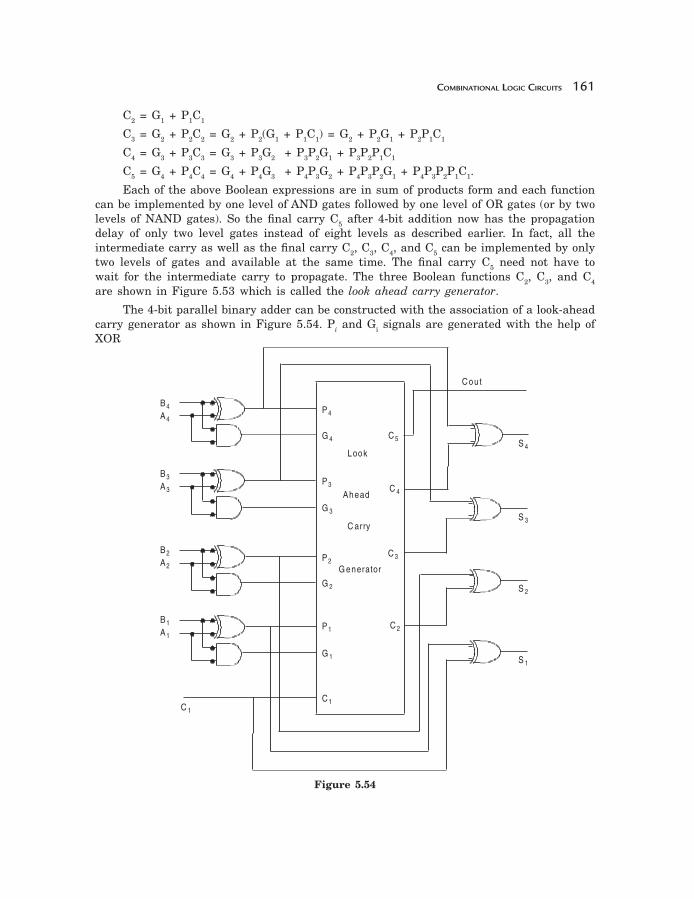
The addition of two binary numbers in parallel implies that all the bits of both augend and addend are available at the same time for computation. In any combinational network, the correct output is available only after the signal propagates through all the gates of its concern. Every logic gate offers some delay when the signal passes from its input to output, which is called the propagation delay of the logic gate. So every combinational circuit takes some time to produce its correct output after the arrival of all the input, which is called total propagation time and is equal to the propagation delay of individual gates times the number of gate levels in the circuit. In a 4-bit binary parallel adder, carry generated from the fi rst full adder is added to the next full adder, carry generated form here is added to the next full adder and so on (refer to Figure 5.48). Therefore, the steady state of fi nal carry is available after the signal propagating through four full adder stages and suffers the longest propagation delay with comparison to the sum outputs, as the sum outputs are produced after the signal propagation of only one full adder stage.
The number of gate levels for the carry propagation can be found from the circuit of full adder. The circuit shown in Figure 5.7 is redrawn in Figure 5.52 for convenience. The input and output variables use the subscript i to denote a typical stage in the parallel adder. In Figure 5.52, Pi and Gi represent the intermediate signals settling to their steady sate values after the propagation through the respective gates and common to all full adders and depends only on the input augend and addend bits. The signal from input carry Ci
to output carry Ci+1 propagates through two gate levels—an AND gate and an OR gate. Therefore, for a four-bit parallel adder, the fi nal carry will be available after propagating through 2 × 4 = 8 gate levels. For an n-bit parallel adder there will be 2n number of gate levels to obtain the fi nal carry to its steady state.
Figure 5.52
B3 A3B2 A2B1 B0 A1 A0Add'/Subtract
Cout
Addend B its Augend B its
S4
S4
S3
S3
S2
S2
S1
S1
Cin4-BIT BINA RY ADDER
A i
B i
C i
G i
P i S i
C i+1

160 DIGITAL PRINCIPLES AND LOGIC DESIGN
Although any combinational network will always have some value at the output terminals, the outputs should not be considered correct unless the signals are given enough time to propagate through all the gates required for computation from input stage to output. For a 4-bit parallel binary adder, carry propagation plays an important role as it takes the longest propagation time. Since all other arithmetic operations are implemented by successive addition process, the time consumed during the addition process is very critical. One obvious method to reduce the propagation delay time is to use faster gates. But this is not always the practical solution because the physical circuits have a limit to their capability. Another technique is to employ a little more complex combinational circuit, which can reduce the carry propagation delay time. There are several techniques for the reduction of carry propagation delay time. However, the most widely used method employs the principle of look ahead carry generation, which is illustrated below.
5.9.4 Look-ahead Carry Generator
Consider the full adder circuit in Figure 5.52. Two intermediate variables are defi ned as Pi and Ci such that
Pi = Ai ⊕ Bi and Gi = AiBi.
The output sum and carry can be expressed in terms of Pi and Gi as
Si = Pi ⊕ Ci and Ci+1 = Gi + PiCi.
Gi is called the carry generate and it generates an output carry if both the inputs Ai
and Bi are logic 1, regardless of the input carry. Pi is called the carry propagate because it is the term associated with the propagation of the carry from Ci to Ci+1.
Figure 5.53
Now the Boolean expressions for the carry output of each stage can be written after substituting Ci and Ci+1 as
P 3
G 3
P 2
G 2
P 1
G 1
C 1
C 2
C 3
C 4
COMBINATIONAL LOGIC CIRCUITS 161
C2 = G1 + P1C1
C3 = G2 + P2C2 = G2 + P2(G1 + P1C1) = G2 + P2G1 + P2P1C1
C4 = G3 + P3C3 = G3 + P3G2 + P3P2G1 + P3P2P1C1
C5 = G4 + P4C4 = G4 + P4G3 + P4P3G2 + P4P3P2G1 + P4P3P2P1C1.
Each of the above Boolean expressions are in sum of products form and each function can be implemented by one level of AND gates followed by one level of OR gates (or by two levels of NAND gates). So the fi nal carry C5 after 4-bit addition now has the propagation delay of only two level gates instead of eight levels as described earlier. In fact, all the intermediate carry as well as the fi nal carry C2, C3, C4, and C5 can be implemented by only two levels of gates and available at the same time. The fi nal carry C5 need not have to wait for the intermediate carry to propagate. The three Boolean functions C2, C3, and C4
are shown in Figure 5.53 which is called the look ahead carry generator.
The 4-bit parallel binary adder can be constructed with the association of a look-ahead carry generator as shown in Figure 5.54. Pi and Gi signals are generated with the help of XOR
Figure 5.54
P4
G 4
Cout
B4
B3
B2
B1
A4
A3
A2
A1
P3
G 3
P2
P1
G 2
G 1
C 4
C 3
C 2
C 1C 1
Look
C 5S 4
S 3
S 2
S 1
Ahead
C arry
G enerator
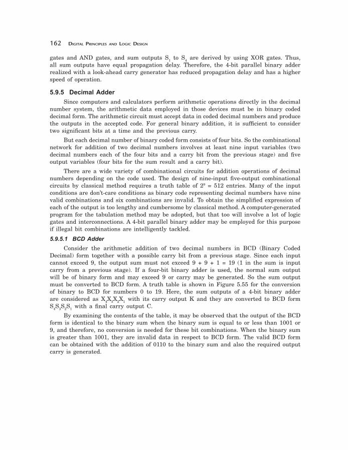
162 DIGITAL PRINCIPLES AND LOGIC DESIGN
gates and AND gates, and sum outputs S1 to S4 are derived by using XOR gates. Thus, all sum outputs have equal propagation delay. Therefore, the 4-bit parallel binary adder realized with a look-ahead carry generator has reduced propagation delay and has a higher speed of operation.
5.9.5 Decimal Adder
Since computers and calculators perform arithmetic operations directly in the decimal number system, the arithmetic data employed in those devices must be in binary coded decimal form. The arithmetic circuit must accept data in coded decimal numbers and produce the outputs in the accepted code. For general binary addition, it is suffi cient to consider two signifi cant bits at a time and the previous carry.
But each decimal number of binary coded form consists of four bits. So the combinational network for addition of two decimal numbers involves at least nine input variables (two decimal numbers each of the four bits and a carry bit from the previous stage) and fi ve output variables (four bits for the sum result and a carry bit).
There are a wide variety of combinational circuits for addition operations of decimal numbers depending on the code used. The design of nine-input fi ve-output combinational circuits by classical method requires a truth table of 29 = 512 entries. Many of the input conditions are don’t-care conditions as binary code representing decimal numbers have nine valid combinations and six combinations are invalid. To obtain the simplifi ed expression of each of the output is too lengthy and cumbersome by classical method. A computer-generated program for the tabulation method may be adopted, but that too will involve a lot of logic gates and interconnections. A 4-bit parallel binary adder may be employed for this purpose if illegal bit combinations are intelligently tackled.
5.9.5.1 BCD Adder
Consider the arithmetic addition of two decimal numbers in BCD (Binary Coded Decimal) form together with a possible carry bit from a previous stage. Since each input cannot exceed 9, the output sum must not exceed 9 + 9 + 1 = 19 (1 in the sum is input carry from a previous stage). If a four-bit binary adder is used, the normal sum output will be of binary form and may exceed 9 or carry may be generated. So the sum output must be converted to BCD form. A truth table is shown in Figure 5.55 for the conversion of binary to BCD for numbers 0 to 19. Here, the sum outputs of a 4-bit binary adder are considered as X4X3X2X1 with its carry output K and they are converted to BCD form S4S3S2S1 with a fi nal carry output C.
By examining the contents of the table, it may be observed that the output of the BCD form is identical to the binary sum when the binary sum is equal to or less than 1001 or 9, and therefore, no conversion is needed for these bit combinations. When the binary sum is greater than 1001, they are invalid data in respect to BCD form. The valid BCD form can be obtained with the addition of 0110 to the binary sum and also the required output carry is generated.

COMBINATIONAL LOGIC CIRCUITS 163
Decimal Binary sum BCD sum
K X4 X3 X2 X1 C S4 S3 S2 S1
0 0 0 0 0 0 0 0 0 0 0
1 0 0 0 0 1 0 0 0 0 1
2 0 0 0 1 0 0 0 0 1 0
3 0 0 0 1 1 0 0 0 1 1
4 0 0 1 0 0 0 0 1 0 0
5 0 0 1 0 1 0 0 1 0 1
6 0 0 1 1 0 0 0 1 1 0
7 0 0 1 1 1 0 0 1 1 1
8 0 1 0 0 0 0 1 0 0 0
9 0 1 0 0 1 0 1 0 0 1
10 0 1 0 1 0 1 0 0 0 0
11 0 1 0 1 1 1 0 0 0 1
12 0 1 1 0 0 1 0 0 1 0
13 0 1 1 0 1 1 0 0 1 1
14 0 1 1 1 0 1 0 1 0 0
15 0 1 1 1 1 1 0 1 0 1
16 1 0 0 0 0 1 0 1 1 0
17 1 0 0 0 1 1 0 1 1 1
18 1 0 0 1 0 1 1 0 0 0
19 1 0 0 1 1 1 1 0 0 1
Figure 5.55
A logic circuit is necessary to detect the illegal binary sum output and can be derived from the table entries. It is obvious that correction is needed when the binary sum produces an output carry K = 1, and for six illegal combinations from 1010 to 1111. Let us consider a logic function Y is generated when the illegal data is detected. A Karnaugh map is prepared for
X2′X1′ X2′X1 X2X1 X2X1′
X4′X3′
X4′X3
X4X3 1 1 1 1
X4X3′ 1 1
Figure 5.56
164 DIGITAL PRINCIPLES AND LOGIC DESIGN
Y with the variables X4, X3, X2, and X1 in Figure 5.56. The output carry K is left aside as we know correction must be done when K = 1. The simplifi ed Boolean expression for Y with variables X4, X3, X2, and X1 is
Y = X4X3 + X4X2.
As the detection logic is also 1 for K = 1, the fi nal Boolean expression of Y taking the variable K into account will be
Y = K + X4X3 + X4X2.
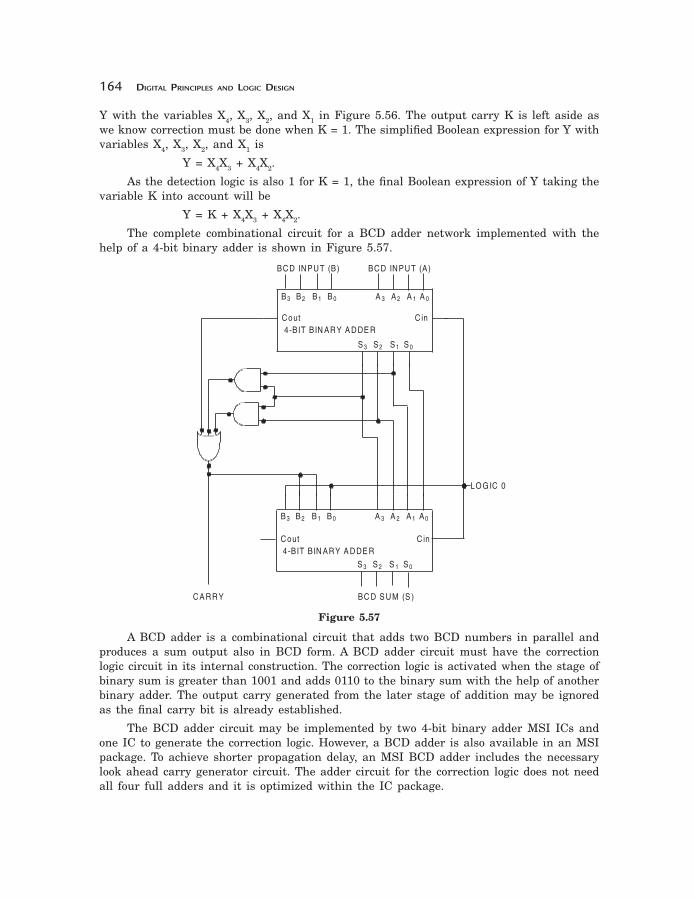
The complete combinational circuit for a BCD adder network implemented with the help of a 4-bit binary adder is shown in Figure 5.57.
Figure 5.57
A BCD adder is a combinational circuit that adds two BCD numbers in parallel and produces a sum output also in BCD form. A BCD adder circuit must have the correction logic circuit in its internal construction. The correction logic is activated when the stage of binary sum is greater than 1001 and adds 0110 to the binary sum with the help of another binary adder. The output carry generated from the later stage of addition may be ignored as the fi nal carry bit is already established.
The BCD adder circuit may be implemented by two 4-bit binary adder MSI ICs and one IC to generate the correction logic. However, a BCD adder is also available in an MSI package. To achieve shorter propagation delay, an MSI BCD adder includes the necessary look ahead carry generator circuit. The adder circuit for the correction logic does not need all four full adders and it is optimized within the IC package.
B3 B2 A 3B1 A2B0 A 1
S3 S2 S1
C in4-BIT BIN ARY A DDE R
Cout
BCD INPUT (B) BCD INPUT (A)
LO G IC 0
C in4-BIT BIN ARY A DDE R
Cout
CA RRY BC D S UM (S )
A 0
S0
B3 B2 A 3B1 A 2B0 A1
S3 S2 S 1
A0
S0

A decimal parallel adder of n decimal digits requires n numbers of BCD adder stages. The output carry from one stage must be connected to the input carry of the next higher order stage.
5.9.6 Parallel Multiplier
To understand the multiplication process, let us consider the multiplication of two 4-bit binary numbers, say 1101 and 1010.
1 1 0 1 → Multiplicand
× 1 0 1 0 → Multiplier
0 0 0 0
1 1 0 1 Partial Products
0 0 0 0
1 1 0 1
1 0 0 0 0 0 1 0 → Final Product
From the above multiplication process, one can easily understand that if the multiplier bit is 1, the multiplicand is simply copied as a partial product. If the multiplicand bit is 0, partial product is 0. Whenever a partial product is obtained, it is placed by shifting one bit left to the previous partial product. After obtaining all the partial products and placing them in the above manner, they are added to get the fi nal product. The multiplication, as illustrated above, can be implemented by a 4-bit binary adder. Figure 5.58 demonstrates a 4-bit binary parallel multiplier using three 4-bit adders and sixteen 2-input AND gates. Here, each group of four AND gates is used to obtain partial products while 4-bit parallel adders are used to add the partial products.
The operation of the 4-bit parallel multiplier is explained in symbolic form of a binary multiplication process as follows.
X3 X2 X1 X0 Multiplicand
Y3 Y2 Y1 Y0 Multiplier
X3 Y0 X2 Y0 X1 Y0 X0 Y0 Partial Product
X3 Y1 X2 Y1 X1 Y1 X0 Y1 Partial Product
C2 C1 C0
C3 S3 S2 S1 S0 Addition
X3 Y2 X2 Y2 X1 Y2 X0 Y2 Partial Product
C6 C5 C4
C7 S7 S6 S5 S4 Addition
X3 Y3 X2 Y3 X1Y3 X0Y3 Partial Product
C10 C9 C8
C11 S11 S10 S9 S8 Addition
M7 M6 M5 M4 M3 M2 M1 M0 Final Product
COMBINATIONAL LOGIC CIRCUITS 165

166 DIGITAL PRINCIPLES AND LOGIC DESIGN
Figure 5.58
M 7 M 5 M 4 M 3
C in
C in
C in
X3
Cout
Cout
Cout
4-B it B inary A dder
4-B it B inary A dder
4-B it B inary A dder
X2 X1
Y 3
Y 2
Y 1
Y 0
X 0
M 2 M 1 M 0M 6
B3 B 2 A3B1 A2B0 A1
S 3 S2 S1
A 0
S0
B3 B2 A3B1 A2B0 A 1
S3 S2 S1
A0
S0
B3 B2 A3B 1 A2B0 A1
S3 S 2 S 1
A0
S 0
X3 X2 X1 X 0
X 3 X 2 X 1 X0
X3 X 2 X1 X 0

COMBINATIONAL LOGIC CIRCUITS 167
5.10 MAGNITUDE COMPARATOR
A magnitude comparator is one of the useful combinational logic networks and has wide applications. It compares two binary numbers and determines if one number is greater than, less than, or equal to the other number. It is a multiple output combinational logic circuit. If two binary numbers are considered as A and B, the magnitude comparator gives three outputs for A > B, A < B, and A = B.
For comparison of two n-bit numbers, the classical method to achieve the Boolean expressions requires a truth table of 22n entries and becomes too lengthy and cumbersome. It is also desired to have a digital circuit possessing with a certain amount of regularity, so that similar circuits can be applied for the comparison of any number of bits. Digital functions that follow an inherent well-defi ned regularity can usually be developed by means of algorithmic procedure if it exists. An algorithm is a process that follows a fi nite set of steps to arrive at the solution to a problem. A method is illustrated here by deriving an algorithm to design a 4-bit magnitude comparator.
The algorithm is the direct application of the procedure to compare the relative magnitudes of two binary numbers. Let us consider the two binary numbers A and B are expanded in terms of bits in descending order as
A = A4A3A2A1
B = B4B3B2B1,
where each subscripted letter represents one of the digits in the number. It is observed from the bit contents of the two numbers that A = B when A4 = B4, A3 = B3, A2 = B2, and A1 = B1. As the numbers are binary they possess the value of either 1 or 0, the equality relation of each pair can be expressed logically by the equivalence function as
Xi = AiBi + Ai′Bi′ for i = 1, 2, 3, 4.
Or, Xi = (A⊕B)′. Or, Xi ′ = A ⊕ B.
Or, Xi = (AiBi′ + Ai′Bi)′.Xi is logic 1 when both Ai and Bi are equal i.e., either 1 or 0 at the same instant. To
satisfy the equality condition of two numbers A and B, it is necessary that all Xi must be equal to logic 1. This dictates the AND operation of all Xi variables. In other words, we can write the Boolean expression for two equal 4-bit numbers
F (A = B) = X4X3X2X1.
To determine the relative magnitude of two numbers A and B, the relative magnitudes of pairs of signifi cant bits are inspected from the most signifi cant position. If the two digits of the most signifi cant position are equal, the next signifi cant pair of digits are compared. The comparison process is continued until a pair of unequal digits is found. It may be concluded that A>B, if the corresponding digit of A is 1 and B is 0. On the other hand, A<B if the corresponding digit of A is 0 and B is 1. Therefore, we can derive the logical expression of such sequential comparison by the following two Boolean functions,
F (A>B) = A4B4′ +X4A3B3′ +X4X3A2B2′ +X4X3X2A1B1′ and
F (A<B) = A4′B4 +X4A3′B3 +X4X3A2′B2 +X4X3X2A1′B1.
The logic gates implementation for the above expressions are not too complex as they contains many subexpressions of a repetitive nature and can be used at different places. The complete logic diagram of a 4-bit magnitude comparator is shown in Figure 5.59. This is a
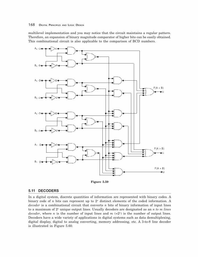
168 DIGITAL PRINCIPLES AND LOGIC DESIGN
multilevel implementation and you may notice that the circuit maintains a regular pattern. Therefore, an expansion of binary magnitude comparator of higher bits can be easily obtained. This combinational circuit is also applicable to the comparison of BCD numbers.
Figure 5.59
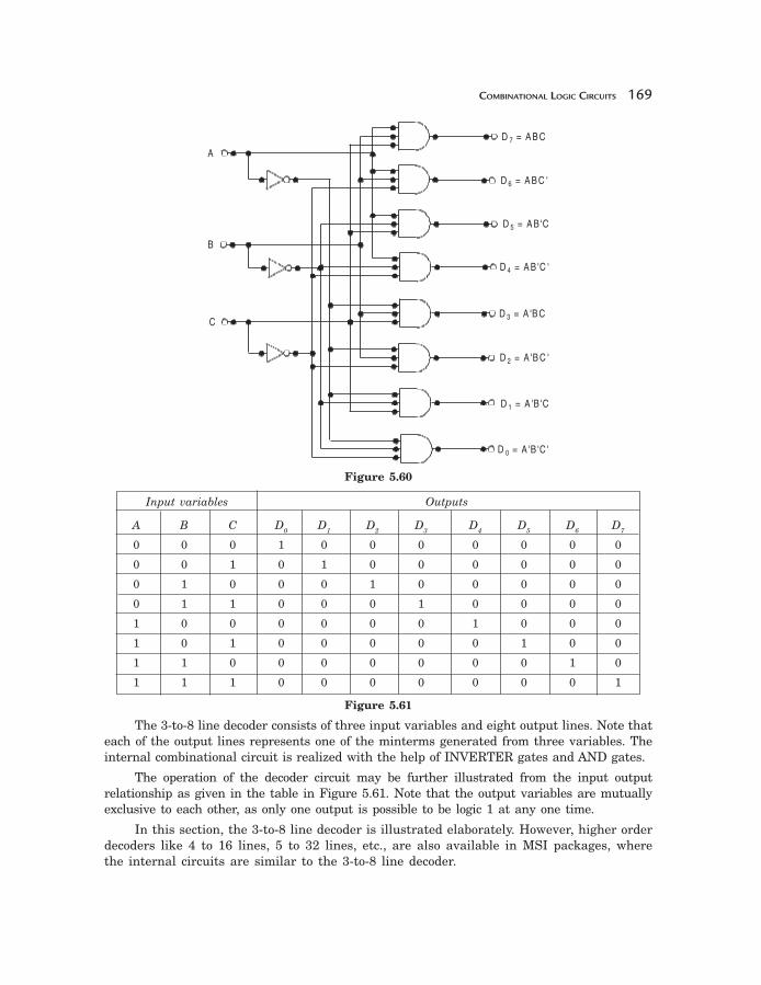
5.11 DECODERS
In a digital system, discrete quantities of information are represented with binary codes. A binary code of n bits can represent up to 2n distinct elements of the coded information. A decoder is a combinational circuit that converts n bits of binary information of input lines to a maximum of 2n unique output lines. Usually decoders are designated as an n to m lines decoder, where n is the number of input lines and m (=2n) is the number of output lines. Decoders have a wide variety of applications in digital systems such as data demultiplexing, digital display, digital to analog converting, memory addressing, etc. A 3-to-8 line decoder is illustrated in Figure 5.60.
F (A < B )
F (A > B )
F (A = B )
A4
B4
A3
B3
A2
B2
A1
B1
COMBINATIONAL LOGIC CIRCUITS 169
Figure 5.60
Input variables Outputs
A B C D0 D1 D2 D3 D4 D5 D6 D7
0 0 0 1 0 0 0 0 0 0 0
0 0 1 0 1 0 0 0 0 0 0
0 1 0 0 0 1 0 0 0 0 0
0 1 1 0 0 0 1 0 0 0 0
1 0 0 0 0 0 0 1 0 0 0
1 0 1 0 0 0 0 0 1 0 0
1 1 0 0 0 0 0 0 0 1 0
1 1 1 0 0 0 0 0 0 0 1
Figure 5.61
The 3-to-8 line decoder consists of three input variables and eight output lines. Note that each of the output lines represents one of the minterms generated from three variables. The internal combinational circuit is realized with the help of INVERTER gates and AND gates.
The operation of the decoder circuit may be further illustrated from the input output relationship as given in the table in Figure 5.61. Note that the output variables are mutually exclusive to each other, as only one output is possible to be logic 1 at any one time.
In this section, the 3-to-8 line decoder is illustrated elaborately. However, higher order decoders like 4 to 16 lines, 5 to 32 lines, etc., are also available in MSI packages, where the internal circuits are similar to the 3-to-8 line decoder.
A
B
C
D = A 'B 'C '0
D = A 'B 'C1
D = A 'B C '2
D = A 'B C3
D = A B 'C5
D = A B C '6
D = A B C7
D = A B 'C '4

170 DIGITAL PRINCIPLES AND LOGIC DESIGN
5.11.1 Some Applications of Decoders
As we have seen that decoders give multiple outputs equivalent to the minterms corresponding to the input variables, it is obvious that any Boolean expression in the sum of the products form can be very easily implemented with the help of decoders. It is not necessary to obtain the minimized expression through simplifying procedures like a Karnaugh map, or tabulation method, or any other procedure. It is suffi cient to inspect the minterm contents of a function from the truth table, or the canonical form of sum of the products of a Boolean expression and selected minterms obtained from the output lines of a decoder may be simply OR-gated to derive the required function. The following examples will demonstrate this.
Example 5.7. Implement the function F (A,B,C) = Σ (1,3,5,6).
Solution. Since the above function has three input variables, a 3-to-8 line decoder may be employed. It is in the sum of the products of the minterms m1, m3, m5, and m6, and so decoder output D1, D3, D5, and D6 may be OR-gated to achieve the desired function. The combinational circuit of the above functions is shown in Figure 5.62.
Figure 5.62
Figure 5.63
Example 5.8. Design a full adder circuit with decoder IC.
Solution. We have seen that full adder circuits are implemented with logic gates in Section 5.3.2. This can be very easily implemented with the help of a decoder IC. Observe the truth table of a full adder in Figure 5.4. In respect to minterms, the Boolean expression of sum output S and carry output C can be written as:
A
B
C
E N
3-TO -8D E C O D E R
L O G IC 1
F
DDDDDDD
7654321
D 0
A
B
C
E N
3-T O -8D E C O D E R
L O G IC 1
B
A
X
S
C
DDDDDDD
7654321
D 0

COMBINATIONAL LOGIC CIRCUITS 171
S = X′A′B + X′AB′ + XA′B′ + XAB and C = X′AB + XA′B + XAB′ + XAB.The above expression can be realized in Figure 5.63.Example 5.9. Similarly, a full-subtractor as described at Section 5.4.2 can be developed
with the help of decoder. From the truth table in Figure 5.10 the Difference D and Borrow B outputs may be written as
D = X′Y′Z + X′YZ′ + XY′Z′ + XYZ and B = X′Y′Z + X′YZ′ + X′YZ + XYZ.The combinational circuit with decoder is shown in Figure 5.64.
Figure 5.64
Example 5.10. Design a BCD-to-decimal decoder with the use of a decoder.
Solution. BCD code uses four bits to represent its different numbers from 0 to 9. So the decoder should have four input lines and ten output lines. By simple method a BCD-to-decimal coder may use a 4-to-16 line decoder. But at output, six lines are illegal and they are deactivated with the use of AND gates or any other means. However, a 3-to-8 line decoder may be employed for this purpose with its intelligent utilization. A partial truth table of a BCD-to-decimal decoder is shown in Figure 5.65.
Input variables Output
A B C D D0 D1 D2 D3 D4 D5 D6 D7 D8 D9
0 0 0 0 1 0 0 0 0 0 0 0 0 0
0 0 0 1 0 1 0 0 0 0 0 0 0 0
0 0 1 0 0 0 1 0 0 0 0 0 0 0
0 0 1 1 0 0 0 1 0 0 0 0 0 0
0 1 0 0 0 0 0 0 1 0 0 0 0 0
0 1 0 1 0 0 0 0 0 1 0 0 0 0
0 1 1 0 0 0 0 0 0 0 1 0 0 0
0 1 1 1 0 0 0 0 0 0 0 1 0 0
1 0 0 0 0 0 0 0 0 0 0 0 1 0
1 0 0 1 0 0 0 0 0 0 0 0 0 1
Figure 5.65
A
B
C
E N
3-TO -8D E C O D E R
L O G IC 1
Z
Y
X
D
B
DDDDDDD
7654321
D 0

172 DIGITAL PRINCIPLES AND LOGIC DESIGN
Since the circuit has ten outputs, ten Karnaugh maps are drawn to simplify each one of the outputs. However, it would be useful to construct a single map similar to a Karnaugh map indicating the outputs and don’t-care conditions as in Figure 5.66. It can be seen that pairs and groups may be formed considering the don’t-care conditions.
The Boolean expressions of the different outputs may be written as
D0 = A′B′C′D′, D1 = A′B′C′D, D2 = B′CD′, D3 = B′CD, D4 = BC′D′, D5 = BC′D,
D6 = BCD′, D7 = BCD, D8 = AD′. and D9 = AD.
C′D′ C′D CD CD′
A′B′ D0 D1 D3 D2
A′B D4 D5 D7 D6
AB X X X X
AB′ D8 D9 X X
Figure 5.66
Figure 5.67
Figure 5.67 illustrates the complete circuit diagram of a BCD decoder implemented with a 3-to-8 decoder IC, with B, C, and D as input lines to the decoder.
B
A
C
D
E N
3-TO -8D E C O D E R
L O G IC 1
DDDDDDD
7654321
D 0
D
D
D
9
8
0
D
D
D
D
D
D
D
7
6
5
4
3
2
1

COMBINATIONAL LOGIC CIRCUITS 173
Example 5.11. Construct a 3-to-8 line decoder with the use of a 2-to-4 line decoder.
Figure 5.68
Solution. Lower order decoders can be cascaded to build higher order decoders. Normally every commercially available decoder ICs have a special input other than normal working input variables called ENABLE. The use of this ENABLE input is that when activated the complete IC comes to the working condition for its normal functioning. If ENABLE input is deactivated the IC goes to sleep mode, the normal functioning is suspended, and all the outputs become logic 0 irrespective of normal input variables conditions. This behavior of ENABLE input makes good use of a cascade connection as in Figure 5.69 where a 3-to-8 line decoder is demonstrated with a 2-to-4 line decoder. Here input variables are designated as X, Y, and Z, and outputs are denoted as Q0 to Q7. X input is connected to the ENABLE input of one decoder and X is used as an ENABLE input of another decoder. When X is logic 0, a lower decoder is activated and gives output Q0 to Q3 and an upper decoder is activated for X is logic 1, output Q4 to Q7 are available this time.
Figure 5.69
A
A
Y
B
B
Z
X
E N
E N
2-T O -4D E C O D E R
2-T O -4D E C O D E R
Q
Q
Q
Q
7
6
5
4
D
D
D
3
2
1
0D
D
D
D
3
2
1
0D
Q
Q
Q
Q
3
2
1
0
X
Y
Z
W
E N
E N
D TO D8 1 5
D TO D0 7
3-TO -8DE CO DE R
3-TO -8DE CO DE R

174 DIGITAL PRINCIPLES AND LOGIC DESIGN
Example 5.12. Construct a 4-to-16 line decoder using a 3-to-8 line decoder.
Solution. A 4-to-16 line decoder has four input variables and sixteen outputs, whereas a 3-to-8 line decoder consists of three input variables and eight outputs. Therefore, one of the input variables is used as the ENABLE input as demonstrated in Example 5.11. Two 3-to-8 line decoders are employed to realize a 4-to-16 line decoder as shown in Figure 5.69. Input variables are designated as W, X, Y, and Z. W input is used as the ENABLE input of the upper 3-to-8 line decoder, which provides D8 to D16 outputs depending on other input variables X, Y, and Z. W is also used as an ENABLE input at inverted mode to a lower decoder, which provides D0 to D7 outputs.
5.12 ENCODERS
An encoder is a combinational network that performs the reverse operation of the decoder. An encoder has 2n or less numbers of inputs and n output lines. The output lines of an encoder generate the binary code for the 2n input variables. Figure 5.70 illustrates an eight inputs/three outputs encoder. It may also be referred to as an octal-to-binary encoder where binary codes are generated at outputs according to the input conditions. The truth table is given in Figure 5.71.
Figure 5.70
Inputs Outputs
D0 D1 D2 D3 D4 D5 D6 D7 A B C
1 0 0 0 0 0 0 0 0 0 0
0 1 0 0 0 0 0 0 0 0 1
0 0 1 0 0 0 0 0 0 1 0
0 0 0 1 0 0 0 0 0 1 1
0 0 0 0 1 0 0 0 1 0 0
0 0 0 0 0 1 0 0 1 0 1
0 0 0 0 0 0 1 0 1 1 0
0 0 0 0 0 0 0 1 1 1 1
Figure 5.71
A = D + D + D + D4 5 6 7
B = D + D + D + D2 3 6 7
C = D + D + D + D1 3 5 7
D
D
D
D
D
D
D
0
1
2
3
4
5
6
D 7
COMBINATIONAL LOGIC CIRCUITS 175
The encoder in Figure 5.70 assumes that only one input line is activated to logic 1 at any particular time, otherwise the other circuit has no meaning. It may be noted that for eight inputs there are a possible 28 = 256 combinations, but only eight input combinations are useful and the rest are don’t-care conditions. It may also be noted that D0 input is not connected to any of the gates. All the binary outputs A, B, and C must be all 0s in this case. All 0s output may also be obtained if all input variables D0 to D7 are logic 0. This is the main discrepancy of this circuit. This discrepancy can be eliminated by introducing another output indicating the fact that all the inputs are not logic 0.
However, this type of encoder is not available in an IC package because it is not easy to implement with OR gates and not much of the gates are used. The type of encoder available in IC package is called a priority encoder. These encoders establish an input priority to ensure that only highest priority input is encoded. As an example, if both D2 and D4 inputs are logic 1 simultaneously, then output will be according to D4 only i.e., output is 100.
5.13 MULTIPLEXERS OR DATA SELECTORS
A multiplexer is one of the important combinational circuits and has a wide range of applications. The term multiplex means “many into one.” Multiplexers transmit large numbers of information channels to a smaller number of channels. A digital multiplexer is a combinational circuit that selects binary information from one of the many input channels and transmits to a single output line. That is why the multiplxers are also called dataselectors. The selection of the particular input channel is controlled by a set of select inputs. A digital multiplexer of 2n input channels can be controlled by n numbers of select lines and an input line is selected according to the bit combinations of select lines.
Selection Inputs Input Channels Output
S1 S0 I0 I1 I2 I3 Y
0 0 0 X X X 0
0 0 1 X X X 1
0 1 X 0 X X 0
0 1 X 1 X X 1
1 0 X X 0 X 0
1 0 X X 1 X 1
1 1 X X X 0 0
1 1 X X X 1 1
Figure 5.72
A 4-to-1 line multiplexer is defi ned as the multiplexer consisting of four input channels and information of one of the channels can be selected and transmitted to an output line according to the select inputs combinations. Selection of one of the four input channels is possible by two selection inputs. Figure 5.72 illustrates the truth table. Input channels I0,I1, I2, and I3 are selected by the combinations of select inputs S1 and S0. The circuit diagram is shown in Figure 5.73. To demonstrate the operation, let us consider that select input combination S1S0 is 01. The AND gate associated with I1 will have two of inputs equal to logic 1 and a third input is connected to I1. Therefore, output of this AND gate is according
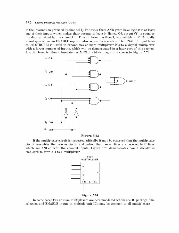
176 DIGITAL PRINCIPLES AND LOGIC DESIGN
to the information provided by channel I1. The other three AND gates have logic 0 to at least one of their inputs which makes their outputs to logic 0. Hence, OR output (Y) is equal to the data provided by the channel I1. Thus, information from I1 is available at Y. Normally a multiplexer has an ENABLE input to also control its operation. The ENABLE input (also called STROBE) is useful to expand two or more multiplexer ICs to a digital multiplexer with a larger number of inputs, which will be demonstrated in a later part of this section. A multiplexer is often abbreviated as MUX. Its block diagram is shown in Figure 5.74.
Figure 5.73
If the multiplexer circuit is inspected critically, it may be observed that the multiplexer circuit resembles the decoder circuit and indeed the n select lines are decoded to 2n lines which are ANDed with the channel inputs. Figure 5.75 demonstrates how a decoder is employed to form a 4-to-1 multiplexer.
Figure 5.74
In some cases two or more multiplexers are accommodated within one IC package. The selection and ENABLE inputs in multiple-unit ICs may be common to all multiplexers.
Y
I
I
I
I
0
1
2
3
S
S
1
0
E N
Y
I
I
I
0
1
2
I3S1 S 0
4-to -1M ULT IPLEX ER
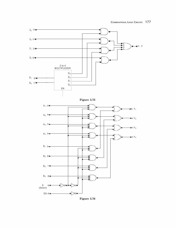
COMBINATIONAL LOGIC CIRCUITS 177
Figure 5.75
Figure 5.76
Y
I
I
I
I
3
2
1
0
S
S
1
0
D 3
D
D
D
2
1
0
2-to -4M ULT IP LEXE R
EN
E N
A1
A
A
A
2
3
4
B
B
B
B
2
3
4
1
S(S elect)
Y
Y
Y
Y
2
3
4
1

178 DIGITAL PRINCIPLES AND LOGIC DESIGN
The internal circuit diagram of a quadruple 2-to-1 multiplexer IC is illustrated in Figure 5.76. It has four multiplexers, each capable of selecting one of two input lines. Either of the inputs A1 or B1 may be selected to provide output at Y1. Similarly, Y2 may have the value of A2 or B2 and so on. One input selection line S is suffi cient to perform the selection operation of one of the two input lines in all four multiplexers. The control input EN enables the multiplexers for their normal function when it is at logic 0 state, and all the multiplexers suspend their functioning when EN is logic 1.
A function table is provided in Figure 5.77. When EN = 1, all the outputs are logic 0, irrespective of any data at inputs I0, I1, I2, or I4. When EN = 0, all the multiplexers become activated, outputs possess the A value if S = 0 and outputs are equal to data at B if S = 1.
E S Output Y
1 X All 0’s
0 0 Select A
0 1 Select B
Figure 5.77
5.13.1 Cascading of Multiplexers
As stated earlier, multiplexers of a larger number of inputs can be implemented by the multiplexers of a smaller number of input lines. Figure 5.78 illustrates that an 8-to-1 line multiplexer is realized by two 4-to-1 line multiplexers.
Figure 5.78
A
B
C
Y
F
X
X
X
0
1
2
X3
I
I
I
0
1
2
I3 S1 S0
4-to -1M UX
EN
X
X
X
4
5
6
X7
I
I
I
0
1
2
I3 S1EN S0
4-to -1M UX

COMBINATIONAL LOGIC CIRCUITS 179
Here, variables B and C are applied to select inputs S1 and S0 of both multiplexers whereas the ENABLE input of the upper multiplexer is connected to A and the lower multiplexer is connected to A. So for A = 0, the upper multiplexer is selected and input lines X0 to X3 are selected according to the selected inputs and data is transmitted to an output through the OR gate. When A = 1, the lower multiplexer is activated and input lines X4 to X7 are selected according to the selected inputs.
Similarly, a 16-to-1 multiplexer may be developed by two 8-to-1 multiplexers as shown in Figure 5.79. Alternatively, a 16-to-1 multiplxer can be realized with fi ve 4-to-1 multiplexers as shown in Figure 5.80.
Figure 5.79
The multiplexer is a very useful MSI function and has various ranges of applications in data communication. Signal routing and data communication are the important applications of a multiplexer. It is used for connecting two or more sources to guide to a single destination among computer units and it is useful for constructing a common bus system. One of the general properties of a multiplexer is that Boolean functions can be implemented by this device, which will be demonstrated here.
EN S 2 S1
IIIIIIII
0
1
2
3
4
5
6
7
8-to -1M UX
Y
S0
IN PUTSX TO X0 7
S 2 S1
IIIIIIII
0
1
2
3
4
5
6
7
8-to -1M UX
Y
S0
IN PUTSX TO X8 1 5
A
B
C
D

180 DIGITAL PRINCIPLES AND LOGIC DESIGN
Figure 5.80
4-TO -1M UXX
X
X
X
0
1
2
3
I
I
I
0
1
2
3I EN S1 S0
4-TO -1M UXX
X
X
X
4
5
6
7
I
I
I
0
1
2
3I EN S1 S0
4-TO -1M UXX
X
X
X
8
9
1 0
11
I
I
I
0
1
2
3I EN S 1 S 0
4-TO -1M UXX
X
X
X
1 2
1 3
1 4
1 5
I
I
I
0
1
2
3I EN S 1 S 0
4-TO -1M UX
ABCD
I
I
I
0
1
2
3I EN S 1 S0
Y
Y
Y
FY
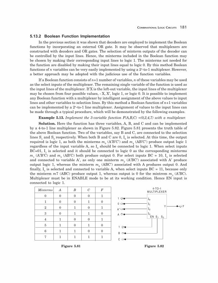
COMBINATIONAL LOGIC CIRCUITS 181
5.13.2 Boolean Function Implementation
In the previous section it was shown that decoders are employed to implement the Boolean functions by incorporating an external OR gate. It may be observed that multiplexers are constructed with decoders and OR gates. The selection of minterm outputs of the decoder can be controlled by the input lines. Hence, the minterms included in the Boolean function may be chosen by making their corresponding input lines to logic 1. The minterms not needed for the function are disabled by making their input lines equal to logic 0. By this method Boolean functions of n variables can be very easily implemented by using a 2n-to-1 multiplexer. However, a better approach may be adopted with the judicious use of the function variables.
If a Boolean function consists of n+1 number of variables, n of these variables may be used as the select inputs of the multiplexer. The remaining single variable of the function is used as the input lines of the multiplexer. If X is the left-out variable, the input lines of the multiplexer may be chosen from four possible values, - X, X′, logic 1, or logic 0. It is possible to implement any Boolean function with a multiplexer by intelligent assignment of the above values to input lines and other variables to selection lines. By this method a Boolean function of n+1 variables can be implemented by a 2n-to-1 line multiplexer. Assignment of values to the input lines can be made through a typical procedure, which will be demonstrated by the following examples.
Example 5.13. Implement the 3-variable function F(A,B,C) = (0,2,4,7) with a multiplexer.
Solution. Here the function has three variables, A, B, and C and can be implemented by a 4-to-1 line multiplexer as shown in Figure 5.82. Figure 5.81 presents the truth table of the above Boolean function. Two of the variables, say B and C, are connected to the selection lines S1 and S0 respectively. When both B and C are 0, I0 is selected. At this time, the output required is logic 1, as both the minterms m0 (A′B′C′) and m4 (AB′C′) produce output logic 1 regardless of the input variable A, so I0 should be connected to logic 1. When select inputs BC=01, I1 is selected and it should be connected to logic 0 as the corresponding minterms m1 (A′B′C) and m5 (AB′C) both produce output 0. For select inputs BC = 10, I2 is selected and connected to variable A′, as only one minterm m2 (A′BC′) associated with A′ produce output logic 1, whereas the minterm m6 (ABC′) associated with A produces output 0. And fi nally, I3 is selected and connected to variable A, when select inputs BC = 11, because only the minterm m7 (ABC) produce output 1, whereas output is 0 for the mintrem m3 (A′BC).Multiplexer must be in ENABLE mode to be at its working condition. Hence EN input is connected to logic 1.
Minterms A B C F
0 0 0 0 1
1 0 0 1 0
2 0 1 0 1
3 0 1 1 0
4 1 0 0 1
5 1 0 1 0
6 1 1 0 0
7 1 1 1 1
Figure 5.81 Figure 5.82
I
I
I
0
1
2
3IEN
Y
S 1 S0
4-TO -1M ULT IP LEXE R
F
1
0
A
A
′
1
B
C
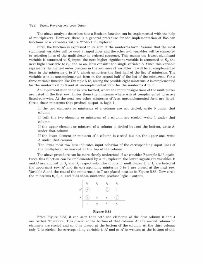
182 DIGITAL PRINCIPLES AND LOGIC DESIGN
The above analysis describes how a Boolean function can be implemented with the help of multiplexers. However, there is a general procedure for the implementation of Boolean functions of n variables with a 2n-1-to-1 multiplexer.
First, the function is expressed in its sum of the minterms form. Assume that the most signifi cant variables will be used at input lines and the other n–1 variables will be connected to selection lines of the multiplexer in ordered sequence. This means the lowest signifi cant variable is connected to S0 input, the next higher signifi cant variable is connected to S1, the next higher variable to S2, and so on. Now consider the single variable A. Since this variable represents the highest order position in the sequence of variables, it will be at complemented form in the minterms 0 to 2n-1, which comprises the fi rst half of the list of minterms. The variable A is at uncomplemented form in the second half of the list of the minterms. For a three-variable function like Example 5.13, among the possible eight minterms, A is complemented for the minterms 0 to 3 and at uncomplemented form for the minterms 4 to 7.
An implementation table is now formed, where the input designations of the multiplexer are listed in the fi rst row. Under them the minterms where A is at complemented form are listed row-wise. At the next row other minterms of A at uncomplemented form are listed. Circle those minterms that produce output to logic 1.
If the two elements or minterms of a column are not circled, write 0 under that column.
If both the two elements or minterms of a column are circled, write 1 under that column.
If the upper element or minterm of a column is circled but not the bottom, write A′under that column.
If the lower element or minterm of a column is circled but not the upper one, write A under that column.
The lower most row now indicates input behavior of the corresponding input lines of the multiplexer as marked at the top of the column.
The above procedure can be more clearly understood if we consider Example 5.13 again. Since this function can be implemented by a multiplexer, the lower signifi cant variables B and C are applied to S1 and S0 respectively. The inputs of multiplexer I0 to I3 are listed at the uppermost row. A′ and its corresponding minterms 0 to 3 are placed at the next row. Variable A and the rest of the minterms 4 to 7 are placed next as in Figure 5.83. Now circle the minterms 0, 2, 4, and 7 as these minterms produce logic 1 output.
Figure 5.83
From Figure 5.83, it can seen that both the elements of the fi rst column 0 and 4 are circled. Therefore, ‘1’ is placed at the bottom of that column. At the second column no elements are circled and so ‘0’ is placed at the bottom of the column. At the third column only ‘2’ is circled. Its corresponding variable is A′ and so A′ is written at the bottom of this
0 1 2 3
I0 I1 I2 I3
A ′
4 5 6 7
1 0 A ′ A
A
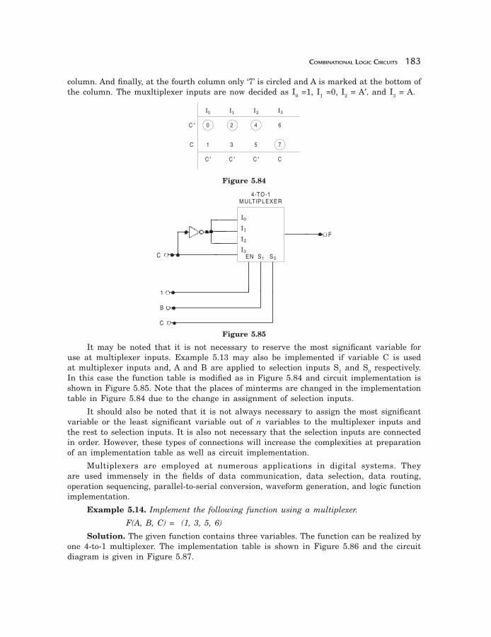
COMBINATIONAL LOGIC CIRCUITS 183
column. And fi nally, at the fourth column only ‘7’ is circled and A is marked at the bottom of the column. The muxltiplexer inputs are now decided as I0 =1, I1 =0, I2 = A′, and I3 = A.
Figure 5.84
Figure 5.85
It may be noted that it is not necessary to reserve the most signifi cant variable for use at multiplexer inputs. Example 5.13 may also be implemented if variable C is used at multiplexer inputs and, A and B are applied to selection inputs S1 and S0 respectively. In this case the function table is modifi ed as in Figure 5.84 and circuit implementation is shown in Figure 5.85. Note that the places of minterms are changed in the implementation table in Figure 5.84 due to the change in assignment of selection inputs.
It should also be noted that it is not always necessary to assign the most signifi cant variable or the least signifi cant variable out of n variables to the multiplexer inputs and the rest to selection inputs. It is also not necessary that the selection inputs are connected in order. However, these types of connections will increase the complexities at preparation of an implementation table as well as circuit implementation.
Multiplexers are employed at numerous applications in digital systems. They are used immensely in the fi elds of data communication, data selection, data routing, operation sequencing, parallel-to-serial conversion, waveform generation, and logic function implementation.
Example 5.14. Implement the following function using a multiplexer.
F(A, B, C) = (1, 3, 5, 6)
Solution. The given function contains three variables. The function can be realized by one 4-to-1 multiplexer. The implementation table is shown in Figure 5.86 and the circuit diagram is given in Figure 5.87.
0 2 4 6
I0 I1 I2 I3
C ′
1 3 5 7
C ′ C ′ C ′ C
C
F
C
I
I
I
0
1
2
3IEN S1 S 0
4-TO -1M ULT IP LEXE R
1
B
C

184 DIGITAL PRINCIPLES AND LOGIC DESIGN
Figure 5.86 Figure 5.87
Example 5.15. Implement the following function with a multiplexer.
F (A, B, C, D) = (0, 1, 3, 4, 8, 9, 15)
Solution. The given function contains four variables. The function can be realized by one 8-to-1 multiplexer. The implementation table is shown in Figure 5.88 and the circuit diagram is given in Figure 5.89.
Figure 5.88
Figure 5.89
0 1 2 3
I0 I1 I2 I3
A '
4 5 6 7
0 1 A A'
A
F
I
I
I
0
1
2
3IEN S1 S0
ABC
4-TO -1M ULT IP LEXE R
5v
0 41 52 63 7
I0 I4I1 I5I2 I6I3 I7
A ′
8 129 1310 1411 15
1 A ′1 00 0A ′ A
A
F
I
I
I
0
1
2
3IEN S1 S0
ABC
4-TO -1M ULT IP LEXE R
5v

COMBINATIONAL LOGIC CIRCUITS 185
Example 5.16. Implement a BCD-to-seven segment decoder with multiplexers.
Solution. A BCD-to-seven segment decoder is already described by classical approach and realized with simple gates. The same circuit can be realized with the help of multiplexers. The truth table of a BCD-to-seven segment decoder (for common cathode type) is repeated here at Figure 5.90 for convenience. As there are four input variables, 4-to-1 multiplexers are employed to develop the combinational logic circuit. Implementation tables for each of the outputs a to g are shown in Figures 5.91(a)-(g). The logic diagram implementation of a BCD-to-seven segment decoder with 4-to-1 multiplexers is shown in Figure 5.92. Note that don’t-care combinations (X) are judiciously considered as logic 1 or logic 0 in the implementation table.
Decimal Input Variables Output Variables as Seven Segment Display
Numbers A B C D a b c d e f g
0 0 0 0 0 1 1 1 1 1 1 0
1 0 0 0 1 0 1 1 0 0 0 0
2 0 0 1 0 1 1 0 1 1 0 1
3 0 0 1 1 1 1 1 1 0 0 1
4 0 1 0 0 0 1 1 0 0 1 1
5 0 1 0 1 1 0 1 1 0 1 1
6 0 1 1 0 0 0 1 1 1 1 1
7 0 1 1 1 1 1 1 0 0 0 0
8 1 0 0 0 1 1 1 1 1 1 1
9 1 0 0 1 1 1 1 0 0 1 1
Figure 5.90 (For a common cathode display.)
Figure 5.91(a) For a.
Figure 5.91(b) For b.
0 41 52 63 7
I0 I4I1 I5I2 I6I3
A ′
8 129 1310 1411 15
1 0
X
A 1
X
1
X
0
X
1
X
1
X
A
0 41 52 63 7A ′
8 129 1310 1411 15
1 1
X
1 0
X
1
X
0
X
1
X
1
X
A
I0 I4I1 I5I2 I6I3

186 DIGITAL PRINCIPLES AND LOGIC DESIGN
Figure 5.91(c) For c.
Figure 5.91(d) For d.
Figure 5.91(e) For e.
Figure 5.91(f) For f.
Figure 5.91(g) For g.
0 41 52 63 7A ′
8 129 1310 1411 15
1 1
X
1 1
X
0
X
1
X
1
X
1
X
A
I0 I4I1 I5I2 I6I3
0 41 52 63 7A ′
8 129 1310 1411 15
1 0
X
0 1
X
1
X
1
X
1
X
0
X
A
I0 I4I1 I5I2 I6I3
0 41 52 63 7A ′
8 129 1310 1411 15
1 0
X
0 0
X
1
X
1
X
0
X
0
X
A
I0 I4I1 I5I2 I6I3
0 41 52 63 7A ′
8 129 1310 1411 15
1 1
X
A 1
X
0
X
1
X
0
X
0
X
A
I0 I4I1 I5I2 I6I3
0 41 52 63 7A ′
8 129 1310 1411 15
A 1
X
A 1
X
1
X
1
X
1
X
0
X
A
I0 I4I1 I5I2 I6I3

COMBINATIONAL LOGIC CIRCUITS 187
Figure 5.92
A B C D LO G IC 1
I7 I6 I5 I4 I3I2 I1 I0ENS2S1S0
8 : 1M UX
Y
a
I7 I6 I5 I4 I3I2 I1 I0ENS2S1S0
8 : 1M UX
Y
b
I7 I6 I5 I4 I3I2 I1 I0ENS2S1S0
8 : 1M UX
Y
c
I7 I6 I5 I4 I3I2 I1 I0ENS2S1S0
8 : 1M UX
Y
d
I7 I6 I5 I4 I3I2 I1 I0ENS2S1S0
8 : 1M UX
Y
e
I7 I6 I5 I4 I3I2 I1 I0ENS 2S 1S 0
8 : 1M UX
Y
f
I7 I6 I5 I4 I3I2 I1 I0ENS 2S 1S 0
8 : 1M UX
Y
g
LO G IC 0

188 DIGITAL PRINCIPLES AND LOGIC DESIGN
5.14 DEMULTIPLEXERS OR DATA DISTRIBUTORS
The term “demultiplex” means one into many. Demultiplexing is the process that receives information from one channel and distributes the data over several channels. It is the reverse operation of the multiplexer. A demultiplexer is the logic circuit that receives information through a single input line and transmits the same information over one of the possible 2n
output lines. The selection of a specifi c output line is controlled by the bit combinations of the selection lines.
Selection Inputs Outputs
A B C Y0 Y1 Y2 Y3 Y4 Y5 Y6 Y7
0 0 0 Y0 = I 0 0 0 0 0 0 0
0 0 1 0 Y1 = I 0 0 0 0 0 0
0 1 0 0 0 Y2 = I 0 0 0 0 0
0 1 1 0 0 0 Y3 = I 0 0 0 0
1 0 0 0 0 0 0 Y4 = I 0 0 0
1 0 1 0 0 0 0 0 Y5 = I 0 0
1 1 0 0 0 0 0 0 0 Y6 = I 0
1 1 1 0 0 0 0 0 0 0 Y7 = I
Figure 5.93
Figure 5.94 Figure 5.95
A
B
C
Y 7
Y 6
Y 5
Y 4
Y 3
Y 2
Y 1
Y 0
I
1-to-8DE M UX
YY
YYY
Y
YY
7
6
5
4
3
2
1
0
I
S2 S1 S0
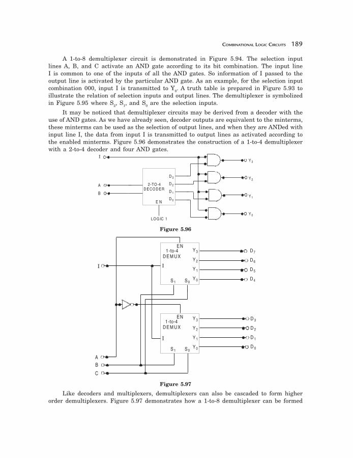
COMBINATIONAL LOGIC CIRCUITS 189
A 1-to-8 demultiplexer circuit is demonstrated in Figure 5.94. The selection input lines A, B, and C activate an AND gate according to its bit combination. The input line I is common to one of the inputs of all the AND gates. So information of I passed to the output line is activated by the particular AND gate. As an example, for the selection input combination 000, input I is transmitted to Y0. A truth table is prepared in Figure 5.93 to illustrate the relation of selection inputs and output lines. The demultiplexer is symbolized in Figure 5.95 where S2, S1, and S0 are the selection inputs.
It may be noticed that demultiplexer circuits may be derived from a decoder with the use of AND gates. As we have already seen, decoder outputs are equivalent to the minterms, these minterms can be used as the selection of output lines, and when they are ANDed with input line I, the data from input I is transmitted to output lines as activated according to the enabled minterms. Figure 5.96 demonstrates the construction of a 1-to-4 demultiplexer with a 2-to-4 decoder and four AND gates.
Figure 5.96
Figure 5.97
Like decoders and multiplexers, demultiplexers can also be cascaded to form higher order demultiplexers. Figure 5.97 demonstrates how a 1-to-8 demultiplexer can be formed
I
E N
A
B
2-TO -4DE CO DE R
D
D
D
D
3
2
1
0
Y
Y
Y
3
2
1
0YLO G IC 1
I
AB
C
D
D
D
D
7
6
5
4
Y
Y
Y
3
2
1
0Y
EN1-to-4
DE M UX
I
S 1 S0
D
D
D
D
3
2
1
0
Y
Y
Y
3
2
1
0Y
EN1-to-4
DE M UX
I
S 1 S0
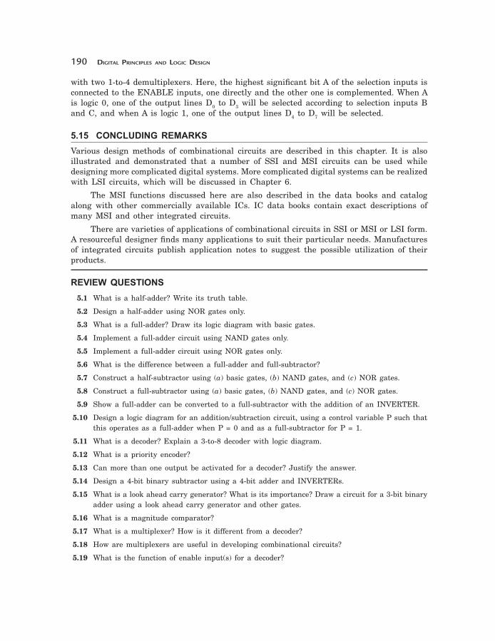
190 DIGITAL PRINCIPLES AND LOGIC DESIGN
with two 1-to-4 demultiplexers. Here, the highest signifi cant bit A of the selection inputs is connected to the ENABLE inputs, one directly and the other one is complemented. When A is logic 0, one of the output lines D0 to D3 will be selected according to selection inputs B and C, and when A is logic 1, one of the output lines D4 to D7 will be selected.
5.15 CONCLUDING REMARKS
Various design methods of combinational circuits are described in this chapter. It is also illustrated and demonstrated that a number of SSI and MSI circuits can be used while designing more complicated digital systems. More complicated digital systems can be realized with LSI circuits, which will be discussed in Chapter 6.
The MSI functions discussed here are also described in the data books and catalog along with other commercially available ICs. IC data books contain exact descriptions of many MSI and other integrated circuits.
There are varieties of applications of combinational circuits in SSI or MSI or LSI form. A resourceful designer fi nds many applications to suit their particular needs. Manufactures of integrated circuits publish application notes to suggest the possible utilization of their products.
REVIEW QUESTIONS
5.1 What is a half-adder? Write its truth table.
5.2 Design a half-adder using NOR gates only.
5.3 What is a full-adder? Draw its logic diagram with basic gates.
5.4 Implement a full-adder circuit using NAND gates only.
5.5 Implement a full-adder circuit using NOR gates only.
5.6 What is the difference between a full-adder and full-subtractor?
5.7 Construct a half-subtractor using (a) basic gates, (b) NAND gates, and (c) NOR gates.
5.8 Construct a full-subtractor using (a) basic gates, (b) NAND gates, and (c) NOR gates.
5.9 Show a full-adder can be converted to a full-subtractor with the addition of an INVERTER.
5.10 Design a logic diagram for an addition/subtraction circuit, using a control variable P such that this operates as a full-adder when P = 0 and as a full-subtractor for P = 1.
5.11 What is a decoder? Explain a 3-to-8 decoder with logic diagram.
5.12 What is a priority encoder?
5.13 Can more than one output be activated for a decoder? Justify the answer.
5.14 Design a 4-bit binary subtractor using a 4-bit adder and INVERTERs.
5.15 What is a look ahead carry generator? What is its importance? Draw a circuit for a 3-bit binary adder using a look ahead carry generator and other gates.
5.16 What is a magnitude comparator?
5.17 What is a multiplexer? How is it different from a decoder?
5.18 How are multiplexers are useful in developing combinational circuits?
5.19 What is the function of enable input(s) for a decoder?

COMBINATIONAL LOGIC CIRCUITS 191
5.20 What are the major applications of multiplexers?
5.21 Design a combinational circuit for a BCD-to-gray code using (a) standard logic gates, (b) decoder, (c) 8-to-1 multiplexer, and (d) 4-to-1 multiplexer.
5.22 Design a combinational circuit for a gray-to-BCD code using (a) standard logic gates, (b) decoder, (c) 8-to-1 multiplexer, and (d) 4-to-1 multiplexer.
5.23 A certain multiplexer can switch one of 32 data inputs to output. How many different inputs does this MUX have?
5.24 An 8-to-1 MUX has inputs A, B, and C connected to selection lines S2, S1, and S0 respectively. The data inputs I0 to I7 are connected as I1 = I2 = I7 = 0, I3 = I5 = 1, I0 = I4 = D, and I6 = D'. Determine the Boolean expression of the MUX output.
5.25 Design an 8-bit magnitude comparator using 4-bit comparators and other gates.
5.26 Implement the Boolean function F(A, B, C, D) = Σ ( 1, 3, 4, 11, 12, 13, 15) using (a) decoder and external gates, and (b) 8-to-1 MUX and external gates.
5.27 Is it possible to implement the Boolean function of problem 5.26 using one 4-to-1 MUX and external gates?
5.28 Design an Excess-3-to-8421 code converter using a 4-to-16 decoder with enable input E' and associated gates.
5.29 Repeat problem 5.28 using 8-to-1 multiplexers.
❑ ❑ ❑