Embed Size (px)
Citation preview
Version: Tentative 0.2
TECHNICAL SPECIFICATION
MODEL NO: 3.7inch e-Paper
The content of this information is subject to be changed without
notice. Please contact Waveshare for further information.
□ Customer’s Confirmation
Customer
Date
By
3.7inch e-Paper
PAGE 1
Revision History Rev. Issued Date Revised Contents
Tentative 0.1 20190516 New
Tentative 0.2 20190517 Add 7-2 Add 9-3
3.7inch e-Paper
PAGE 2
TECHNICAL SPECIFICATION
CONTENTS
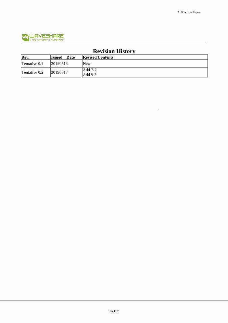
NO. ITEM PAGE - Cover 1
- Revision history 2
- Contents 3
1 General description 4
2 Features 4
3 Mechanical specifications 4
4 Mechanical drawing of EPD module 5
5 Input/Output terminals 6
6 Electrical characteristics 7
7 Power sequence 13
8 Optical characteristics 16
9 SPI command description 17
10 SPI control registers 20
11 Reference circuit 74
12 Handling, safety and environment requirements 75
13 Reliability test 76
14 Border definition and scan direction 77
15 Packing 78
3.7inch e-Paper
PAGE 3
1. General description
This display is a reflective electrophoretic E Ink® technology display module based on glass
active matrix TFT substrate. It has 3.69” active area with 280(H) x 480(V) pixels, the display is
capable to display images at 2 gray levels (1 bit) depending on the display controller and the associated
waveform file it used.
2. Features
� High contrast reflective/electrophoretic technology
� 280(H) x 480(V) display
� High reflectance
� Ultra wide viewing angle
� Ultra low power consumption
� Pure reflective mode
� Bi-stable
� Commercial temperature range
� Portrait pin out. Landscape mode scan.
� Glass substrate.
� All in one IC that integrated source driver, gate driver, TCON, PMIC and OTP memory in the
module. � Built in temperature sensor: On-Chip: -25~50℃ ± 2.0℃ / 8-bit status
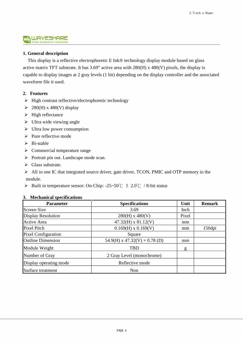
3. Mechanical specificationsParameter Specifications Unit Remark
Screen Size 3.69 Inch Display Resolution 280(H) x 480(V) Pixel Active Area 47.32(H) x 81.12(V) mm Pixel Pitch 0.169(H) x 0.169(V) mm 150dpi Pixel Configuration Square Outline Dimension 54.9(H) x 47.32(V) × 0.78 (D) mm
Module Weight TBD g
Number of Gray 2 Gray Level (monochrome)
Display operating mode Reflective mode
Surface treatment Non
3.7inch e-Paper
PAGE 4

4. Mechanical drawing of EPD module
3.7inch e-Paper
PAGE 5
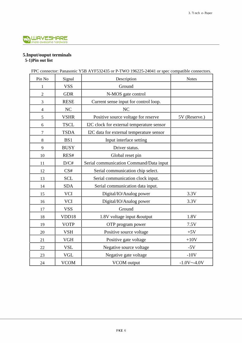
5.Input/ouput terminals 5-1)Pin out list
FPC connector: Panasonic Y5B AYF532435 or P-TWO 196225-24041 or spec compatible connectors.
Pin No Signal Description Notes
1 VSS Ground
2 GDR N-MOS gate control
3 RESE Current sense input for control loop.
4 NC NC
5 VSHR Positive source voltage for reserve 5V (Reserve.)
6 TSCL I2C clock for external temperature sensor
7 TSDA I2C data for external temperature sensor
8 BS1 Input interface setting
9 BUSY Driver status.
10 RES# Global reset pin
11 D/C# Serial communication Command/Data input
12 CS# Serial communication chip select.
13 SCL Serial communication clock input.
14 SDA Serial communication data input.
15 VCI Digital/IO/Analog power 3.3V
16 VCI Digital/IO/Analog power 3.3V
17 VSS Ground
18 VDD18 1.8V voltage input &output 1.8V
19 VOTP OTP program power 7.5V
20 VSH Positive source voltage +5V
21 VGH Positive gate voltage +10V
22 VSL Negative source voltage -5V
23 VGL Negative gate voltage -10V
24 VCOM VCOM output -1.0V~-4.0V
3.7inch e-Paper
PAGE 6
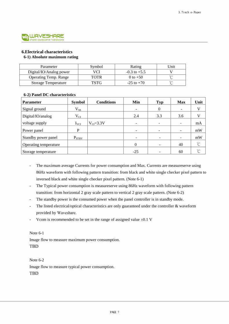
6.Electrical characteristics 6-1) Absolute maximum rating
6-2) Panel DC characteristics
- The maximum average Currents for power consumption and Max. Currents are measureserve using
86Hz waveform with following pattern transition: from black and white single checker pixel pattern to
inversed black and white single checker pixel pattern. (Note 6-1)
- The Typical power consumption is measureserve using 86Hz waveform with following pattern
transition: from horizontal 2 gray scale pattern to vertical 2 gray scale pattern. (Note 6-2)
- The standby power is the consumed power when the panel controller is in standby mode.
- The listed electrical/optical characteristics are only guaranteed under the controller & waveform
provided by Waveshare. - Vcom is recommended to be set in the range of assigned value ±0.1 V
Note 6-1
Image flow to measure maximum power consumption.
TBD
Note 6-2
Image flow to measure typical power consumption.
TBD
Parameter Symbol Rating Unit Digital/IO/Analog power VCI -0.3 to +5.5 V Operating Temp. Range TOTR 0 to +50 ℃
Storage Temperature TSTG -25 to +70 ℃
Parameter Symbol Conditions Min Typ Max Unit
Signal ground VSS - 0 - V
Digital/IO/analog
voltage supply
VCI 2.4 3.3 3.6 V
IVCI VCI=3.3V - - - mA
Power panel P - - - mW
Standby power panel PSTBY - - - mW
Operating temperature 0 - 40 ℃
Storage temperature -25 - 60 ℃
3.7inch e-Paper
PAGE 7
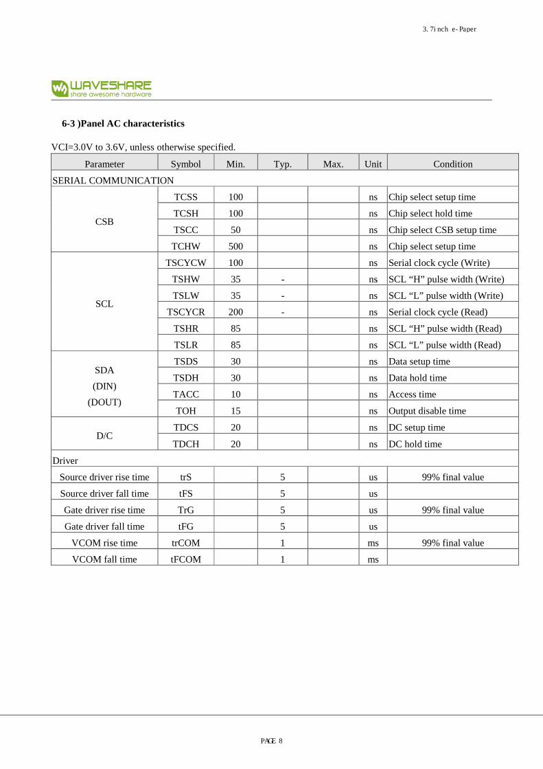
6-3 )Panel AC characteristics
VCI=3.0V to 3.6V, unless otherwise specified.
Parameter Symbol Min. Typ. Max. Unit Condition
SERIAL COMMUNICATION
CSB
TCSS 100 ns Chip select setup time
TCSH 100 ns Chip select hold time
TSCC 50 ns Chip select CSB setup time
TCHW 500 ns Chip select setup time
SCL
TSCYCW 100 ns Serial clock cycle (Write)
TSHW 35 - ns SCL “H” pulse width (Write)
TSLW 35 - ns SCL “L” pulse width (Write)
TSCYCR 200 - ns Serial clock cycle (Read)
TSHR 85 ns SCL “H” pulse width (Read)
TSLR 85 ns SCL “L” pulse width (Read)
SDA
(DIN)
(DOUT)
TSDS 30 ns Data setup time
TSDH 30 ns Data hold time
TACC 10 ns Access time
TOH 15 ns Output disable time
D/C TDCS 20 ns DC setup time
TDCH 20 ns DC hold time
Driver
Source driver rise time trS 5 us 99% final value
Source driver fall time tFS 5 us
Gate driver rise time TrG 5 us 99% final value
Gate driver fall time tFG 5 us
VCOM rise time trCOM 1 ms 99% final value
VCOM fall time tFCOM 1 ms
3.7inch e-Paper
PAGE 8

3.7inch e-Paper
PAGE 9

VIH
VIL
VIH
VIL
Tcss
CSB
SCL
D/C
D7 D6 D0SDA
(DIN)VIH
VIL
4 pin serial interface characteristics (write mode)
D5
TCHWTCSH
TSCC
TDCH
TSCYCW
TSHW
TSLW
TSDHTSDS
TDCS
VIH
VIL
VIH
VIL
Tcss
CSB
SCL
D/C
D7 D6 D0SDA
(DOUT)
4 pin serial interface characteristics (read mode)
D5
TCHWTCSH
TSCC
TDCH
TSCYCW
TSHW
TSLW
TDCS
TACC TOHTACC
Figure 1: SPI interface timing
3.7inch e-Paper
PAGE 10

6-4 )Refresh rate The module is applied at a maximum refresh rate of 50 Hz.
Min Max Refresh Rate - 50 Hz
6-5 ) Data transmission waveform
Example1: LUT all states (7 states) complete or phase number=0, the driver will send 2 frame VCOM and data
to 0 V.
Internal
Vsync
SPI
(input)
I2C
(for EEPROM)
Driver
(action internal)
BUSY_N
VCOM
DATA Frame 1-N DATA Frame 1-N DATA
LUT1
Frame 1-N VCOM
LUT 2
Frame 1-N VCOM
2 frame
Vcom_DC
0V
Display
transmission
Display
transmission ok
Data stop
(11h)
Data start
transmission
(10h and 13h)
LUTC
(20h)LUT Data
(21~24h)
TSC off
(41h)
Floating
Floating
Figure 2: Data transmission example1 waveform
3.7inch e-Paper
PAGE 11

Example2: While level selection in LUT is “11”, the driver will float VCOM and data.
Figure 3: Data transmission example 2 waveform
3.7inch e-Paper
PAGE 12

7. Power sequence7-1)Power on/off sequence
In order to prevent IC fail in power on resetting, the power sequence must be followed as below.
Figure 4: Power on sequence
3.7inch e-Paper
PAGE 13
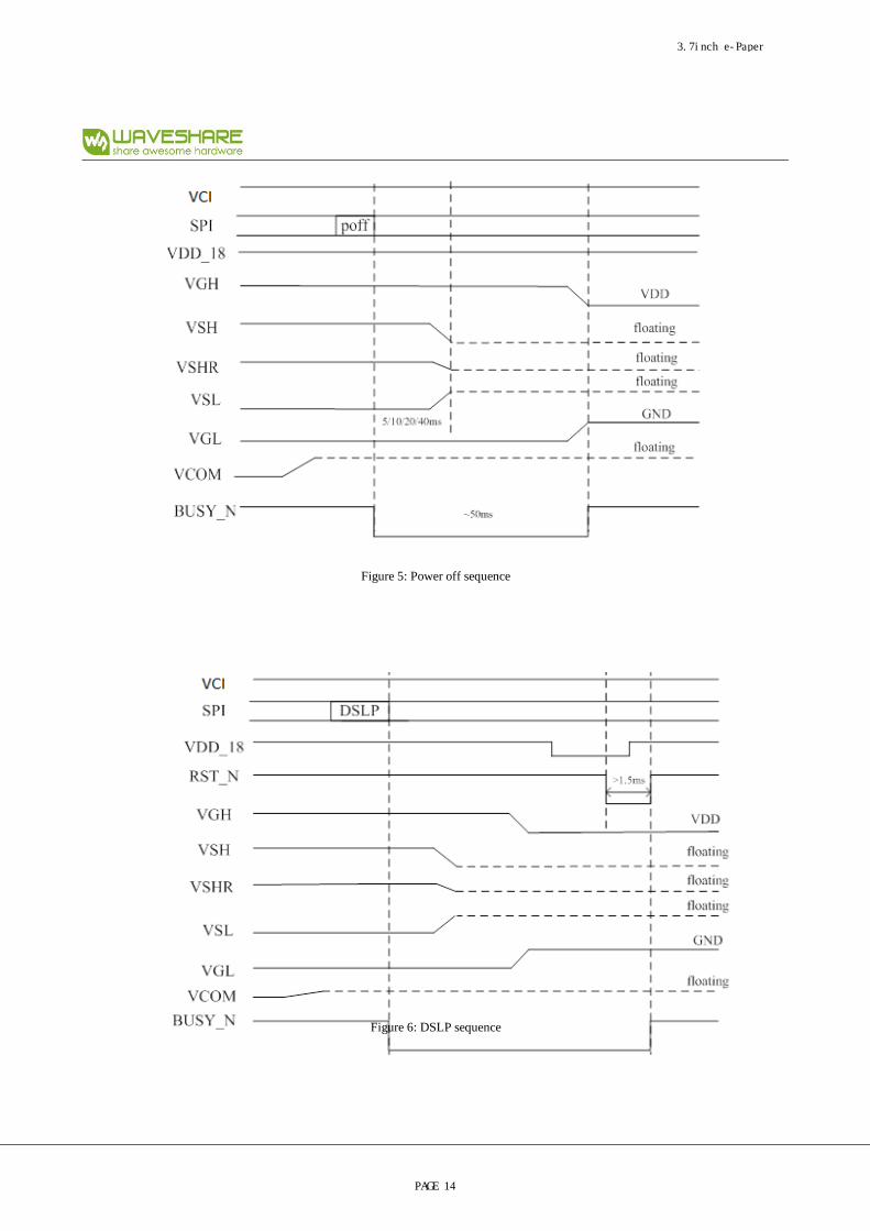
Figure 5: Power off sequence
Figure 6: DSLP sequence
3.7inch e-Paper
PAGE 14
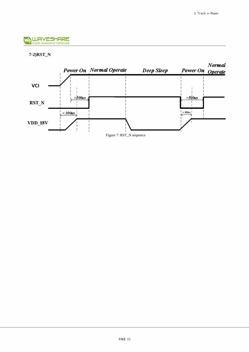
7-2)RST_N
Figure 7: RST_N sequence
3.7inch e-Paper
PAGE 15

8. Optical characteristics
8-1)Specifications
Measurements are made with that the illumination is under an angle of 45 degrees, the detection is
perpendicular unless otherwise specified.
T = 25oC SYMBOL PARAMETER CONDITIONS MIN TYP. MAX UNIT Note
R Reflectance White 25 30 - % Note 9-1
CR Contrast Ratio - 5 7 - -
WS: White state , DS: Dark state
Note 9-1: Spectrum meter: Eye – One Pro Spectrophotometer
8-2)Definition of contrast ratio
The contrast ratio (CR) is the ratio between the reflectance in a full white area (Rl) and the reflectance in a dark
area (Rd): CR = Rl/Rd
45° 45°
Eye–One Spectrophotometer
8-3)Reflection ratio
The reflection ratio is expressed as:
R = Reflectance Factorwhite board x ( Lcenter / Lwhite board )
Lcenter is the luminance measureserve at center in a white area (R=G=B=1). Lwhite board is the luminance of a
standard white board. Both are measureserve with equivalent illumination source. The viewing angle shall be
no more than 2 degrees.
3.7inch e-Paper
PAGE 16
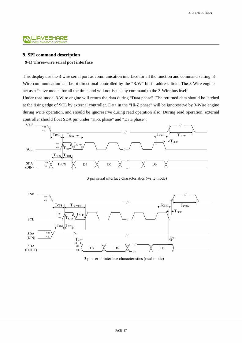
9. SPI command description
9-1) Three-wire serial port interface
This display use the 3-wire serial port as communication interface for all the function and command setting. 3-
Wire communication can be bi-directional controlled by the “R/W” bit in address field. The 3-Wire engine
act as a “slave mode” for all the time, and will not issue any command to the 3-Wire bus itself.
Under read mode, 3-Wire engine will return the data during “Data phase”. The returned data should be latched
at the rising edge of SCL by external controller. Data in the “Hi-Z phase” will be ignoreserve by 3-Wire engine
during write operation, and should be ignoreserve during read operation also. During read operation, external
controller should float SDA pin under “Hi-Z phase” and “Data phase”.
VIH
VIL
VIH
VIL
VIH
VIL
Tcss TSGYCW
TSHW
TSLW
TSDS TSDH
TCSH
TSCC
TCHW
D/CX D7 D6 D0
CSB
SCL
SDA
(DIN)
3 pin serial interface characteristics (write mode)
VIH
VIL
VIH
VIL
VIH
VIL
Tcss TSCYCR
TSHR
TSLR
TSDS TSDH
TCSH
TSCC
TCHW
CSB
SCL
SDA
(DIN)
D7 D6 D0SDA
(DOUT)
VIH
VIL
TACCTOH
3 pin serial interface characteristics (read mode)
3.7inch e-Paper
PAGE 17
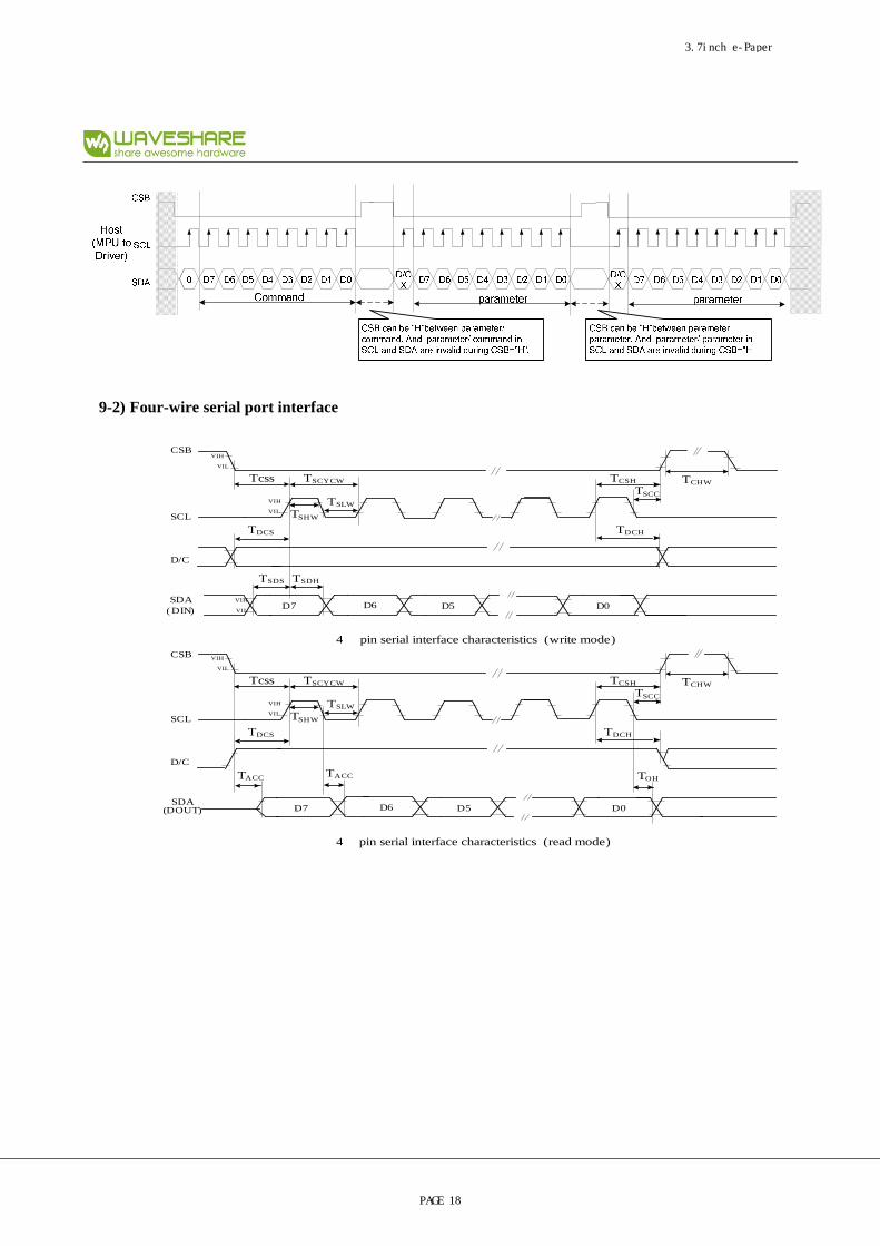
9-2) Four-wire serial port interface
VIH
VIL
VIH
VIL
Tcss
CSB
SCL
D/C
D7 D6 D0SDA
(DIN)VIH
VIL
4 pin serial interface characteristics (write mode)
D5
TCHWTCSH
TSCC
TDCH
TSCYCW
TSHW
TSLW
TSDHTSDS
TDCS
VIH
VIL
VIH
VIL
Tcss
CSB
SCL
D/C
D7 D6 D0SDA
(DOUT)
4 pin serial interface characteristics (read mode)
D5
TCHWTCSH
TSCC
TDCH
TSCYCW
TSHW
TSLW
TDCS
TACC TOHTACC
3.7inch e-Paper
PAGE 18

9-3) Display flow
3.7inch e-Paper
PAGE 19
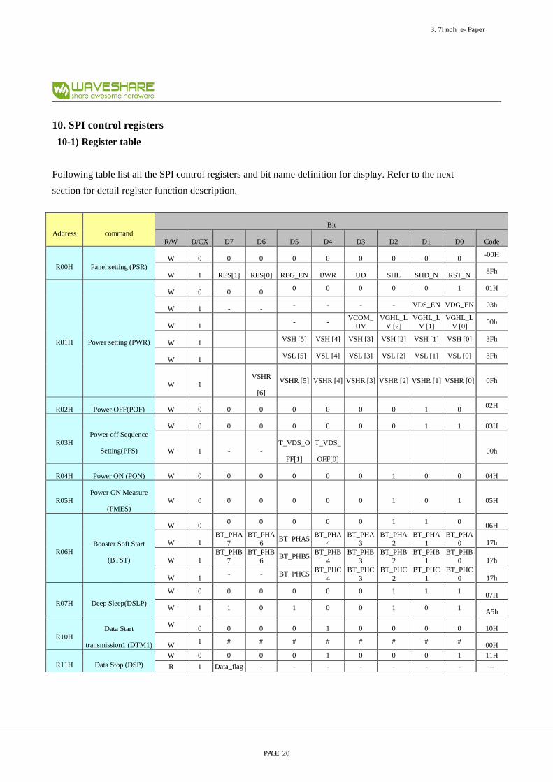
10. SPI control registers
10-1) Register table
Following table list all the SPI control registers and bit name definition for display. Refer to the next
section for detail register function description.
Address command Bit
R/W D/CX D7 D6 D5 D4 D3 D2 D1 D0 Code
R00H Panel setting (PSR) W 0 0 0 0 0 0 0 0 0 -00H
W 1 RES[1] RES[0] REG_EN BWR UD SHL SHD_N RST_N 8Fh
R01H Power setting (PWR)
W 0 0 0 0 0 0 0 0 1 01H
W 1 - - - - - - VDS_EN VDG_EN 03h
W 1 - - VCOM_
HV VGHL_L
V [2] VGHL_L
V [1] VGHL_L
V [0] 00h
W 1 VSH [5] VSH [4] VSH [3] VSH [2] VSH [1] VSH [0] 3Fh
W 1 VSL [5] VSL [4] VSL [3] VSL [2] VSL [1] VSL [0] 3Fh
W 1 VSHR
[6]
VSHR [5] VSHR [4] VSHR [3] VSHR [2] VSHR [1] VSHR [0] 0Fh
R02H Power OFF(POF) W 0 0 0 0 0 0 0 1 0 02H
R03H Power off Sequence
Setting(PFS)
W 0 0 0 0 0 0 0 1 1 03H
W 1 - - T_VDS_O
FF[1]
T_VDS_
OFF[0] 00h
R04H Power ON (PON) W 0 0 0 0 0 0 1 0 0 04H
R05H Power ON Measure
(PMES) W 0 0 0 0 0 0 1 0 1 05H
R06H Booster Soft Start
(BTST)
W 0 0 0 0 0 0 1 1 0 06H
W 1 BT_PHA
7 BT_PHA
6 BT_PHA5
BT_PHA4
BT_PHA3
BT_PHA2
BT_PHA1
BT_PHA0 17h
W 1 BT_PHB
7 BT_PHB
6 BT_PHB5
BT_PHB4
BT_PHB3
BT_PHB2
BT_PHB1
BT_PHB0 17h
W 1 - - BT_PHC5 BT_PHC
4 BT_PHC
3 BT_PHC
2 BT_PHC
1 BT_PHC
0 17h
R07H Deep Sleep(DSLP)
W 0 0 0 0 0 0 1 1 1 07H
W 1 1 0 1 0 0 1 0 1 A5h
R10H Data Start
transmission1 (DTM1)
W 0 0 0 0 1 0 0 0 0 10H
W 1 # # # # # # # # 00H
R11H Data Stop (DSP) W 0 0 0 0 1 0 0 0 1 11H
R 1 Data_flag - - - - - - - --
3.7inch e-Paper
PAGE 20
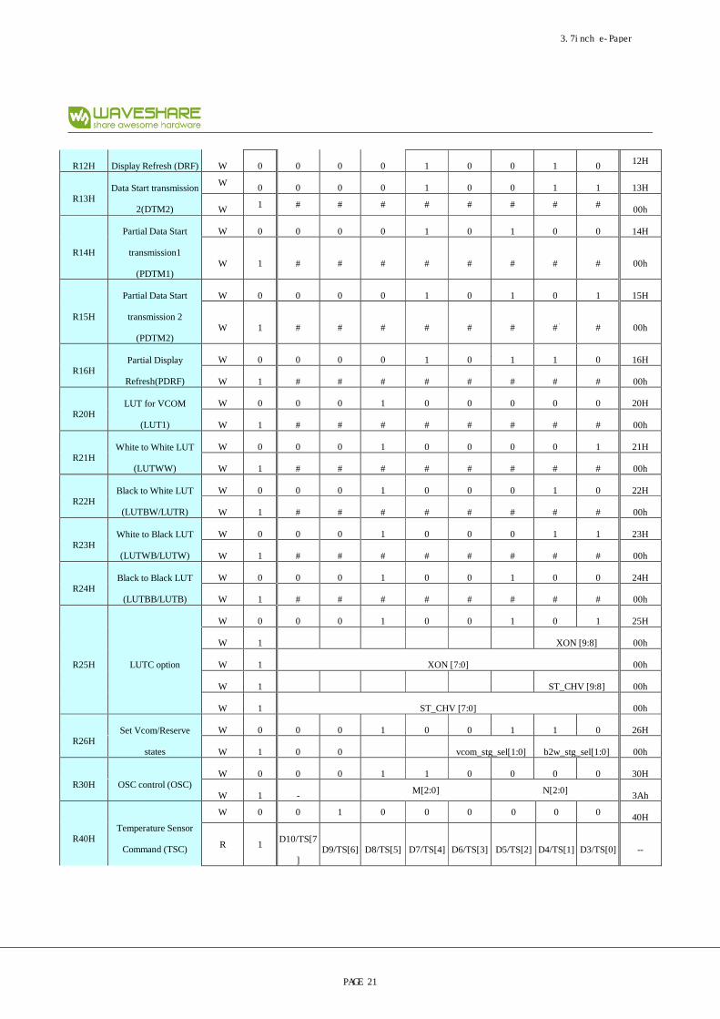
R12H Display Refresh (DRF) W 0 0 0 0 1 0 0 1 0 12H
R13H Data Start transmission
2(DTM2)
W 0 0 0 0 1 0 0 1 1 13H
W 1 # # # # # # # # 00h
R14H
Partial Data Start
transmission1
(PDTM1)
W 0 0 0 0 1 0 1 0 0 14H
W 1 # # # # # # # # 00h
R15H
Partial Data Start
transmission 2
(PDTM2)
W 0 0 0 0 1 0 1 0 1 15H
W 1 # # # # # # # # 00h
R16H Partial Display
Refresh(PDRF)
W 0 0 0 0 1 0 1 1 0 16H
W 1 # # # # # # # # 00h
R20H LUT for VCOM
(LUT1)
W 0 0 0 1 0 0 0 0 0 20H
W 1 # # # # # # # # 00h
R21H White to White LUT
(LUTWW)
W 0 0 0 1 0 0 0 0 1 21H
W 1 # # # # # # # # 00h
R22H Black to White LUT
(LUTBW/LUTR)
W 0 0 0 1 0 0 0 1 0 22H
W 1 # # # # # # # # 00h
R23H White to Black LUT
(LUTWB/LUTW)
W 0 0 0 1 0 0 0 1 1 23H
W 1 # # # # # # # # 00h
R24H Black to Black LUT
(LUTBB/LUTB)
W 0 0 0 1 0 0 1 0 0 24H
W 1 # # # # # # # # 00h
R25H LUTC option
W 0 0 0 1 0 0 1 0 1 25H
W 1 XON [9:8] 00h
W 1 XON [7:0] 00h
W 1 ST_CHV [9:8] 00h
W 1 ST_CHV [7:0] 00h
R26H Set Vcom/Reserve
states
W 0 0 0 1 0 0 1 1 0 26H
W 1 0 0 vcom_stg_sel[1:0] b2w_stg_sel[1:0] 00h
R30H OSC control (OSC) W 0 0 0 1 1 0 0 0 0 30H
W 1 - M[2:0] N[2:0] 3Ah
R40H Temperature Sensor
Command (TSC)
W 0 0 1 0 0 0 0 0 0 40H
R 1 D10/TS[7
] D9/TS[6] D8/TS[5] D7/TS[4] D6/TS[3] D5/TS[2] D4/TS[1] D3/TS[0] --
3.7inch e-Paper
PAGE 21

R 1 D2 D1 D0 - - - - - --
R41H Temperature Sensor
Calibration (TSE)
W 0 0 1 0 0 0 0 0 1 41H
W 1 TSE - - - TO[3] TO[2] TO[1] TO0] 00h
R42H Temperature Sensor
Write (TSW)
W 0 0 1 0 0 0 0 1 0 42H
W 1 WATTR[
7] WATTR[
6] WATTR[5
] WATTR[
4] WATTR[
3] WATTR[2
] WATTR[
1] WATTR[0
] 00h
W 1 WMSB[7
] WMSB[6
] WMSB[5]
WMSB[4]
WMSB[3]
WMSB[2] WMSB[1
] WMSB[0
] 00h
W 1 WLSB[7] WLSB[6] WLSB[5] WLSB[4] WLSB[3] WLSB[2] WLSB[1] WLSB[0] 00h
R43H Temperature Sensor
Read (TSR)
W 0 0 1 0 0 0 0 1 1 43H
R 1 RMSB[7] RMSB[6] RMSB[5] RMSB[4] RMSB[3] RMSB[2] RMSB[1]
RMSB[0] -
R 1 RLSB[7] RLSB[6] RLSB[5] RLSB[4] RLSB[3] RLSB[2] RLSB[1] RLSB[0] -
R50H VCOM and DATA
interval setting (CDI)
W 0 0 1 0 1 0 0 0 0 50H
W 1 VBD[1] VBD[0] DDX[1] DDX[0] CDI[3] CDI[2] CDI[1] CDI[0] D7h
R51H Lower Power Detection
(LPD)
W 0 0 1 0 1 0 0 0 1 51H
R 1 - - - - - - - LPD -
R60H TCON setting (TCON) W 0 0 1 1 0 0 0 0 0 60H
W 1 S2G[3] S2G[2] S2G[1]- S2G[0] G2S[3] G2S[2] G2S[1] G2S[0] 22h
R61H Resolution
setting(TRES)
W 0 0 1 1 0 0 0 0 1 61H
W 1 HRES(7) HRES(6) HRES(5) HRES(4) HRES(3) - - - 00h
W 1 - - - - - - - VRES(8) 00h
W 1 VRES(7) VRES(6) VRES(5) VRES(4) VRES(3) VRES(2) VRES(1) VRES(0) 00h
R62H Source & gate start
setting
W 0 0 1 1 0 0 0 1 0 62H
W 1 S_start
(7) S_start
(6) S_start (5)
S_start (4)
S_start (3)
- - - 00h
W 1 gscan G_start
[8] 00h
W 1 G_start
(7) G_start
(6) G_start (6)
G_start (4)
G_start (3)
G_start (2) G_start
(1) G_start
(0) 00h
R70H REVISION (REV)
W 0 0 1 1 1 0 0 0 0 70H
R 1 REV[7] REV[6] REV[5] REV[4] REV[3] REV[2] REV[1] REV[0] -
R 1 REV[15] REV[14] REV[13] REV[12] REV[11] REV10] REV[09] REV[08] -
R71H Status register(FLG) W 0 0 1 1 1 0 0 0 1 71H
R 1 - PTL_flag I2C_ERR I2C_
BUSYN Data_flag PON POF BUSY_N -
R80H Auto Measure Vcom
(AMV)
W 0 1 0 0 0 0 0 0 0 80 H
W 1 - - AMVT[1] AMVT[0] XON AMVS AMV AMVE 10h
R81H Vcom Value (VV) W 0 1 0 0 0 0 0 0 1 81H
R 1 - - VV[5] VV[4] VV[3] VV[2] VV[1] VV[0] -
3.7inch e-Paper
PAGE 22

R82H Vcom_DC Setting
register(VDCS)
W 0 1 0 0 0 0 0 1 0 82H
W 1 - - VCDS[5] VCDS [4] VCDS [3] VCDS [2] VCDS
[1] VCDS [0] 1Fh
RA0H Program Mode (PGM) W 0 1 0 1 0 0 0 0 0 A0H
W 1 1 0 1 0 0 1 0 1 A5h
RA1H Active program(APG) W 0 1 0 1 0 0 0 0 1 A1H
RA2H Read OTP Data
(ROTP)
W 0 1 0 1 0 0 0 1 0 A2H
R 1 # # # # # # # # -
RE5H Force Temperature
W 0 1 1 1 0 0 1 0 1 E5H
W 1 TS_SET[
7] TS_SET[
6] TS_SET[5
] TS_SET[
4] TS_SET[
3] TS_SET[2
] TS_SET[
1] TS_SET[
0] 00h
RE6H LVD voltage Select
W 0 1 1 1 0 0 1 1 0 E6H
W 1 - - - - - - LVD_SE
L[1] LVD_SEL
[0] 11h
RE7H Panel Break Check
W 0 1 1 1 0 0 1 1 1 E7H
R 1 - - - - - - PSTA -
RE8H Power saving
W 0 1 1 1 0 1 0 0 0 E8H
W 1 VCOM_
W[3] VCOM_
W[2] VCOM_
W[1] VCOM_
W[0] SD_W[3] SD_W[2] SD_W[1] SD_W[0] 00h
RE9H AUTO sequence
W 0 1 1 1 0 1 0 0 1 E9H
W 1 1 0 1 0 0 1 0 1 00h
REBH OTP LUT backup1
program
W 0 1 1 1 0 1 0 1 1 EBH
RECH Read OTP LUT
backup1
W 0 1 1 1 0 1 1 0 0 ECH
R 1 # # # # # # # # --
RESERVE
H
OTP LUT backup2
program
W 0 1 1 1 0 1 1 0 1 EDH
R 1 # # # # # # # # --
REEH Read OTP LUT
backup2
W 0 1 1 1 0 1 1 1 0 EEH
REFH Checksum Program to
OTP
W 0 1 1 1 0 1 1 1 1 EFH
RF0H Remap LUT
W 0 1 1 1 1 0 0 0 0 F0H
W 1 - - - bkup_lut_2_en
rmp2_table_sel[3]
rmp2_table_sel[2]
rmp2_table_sel[1]
rmp2_table_sel[0] 1Fh
W 1 - - - bkup_lut_1_en
rmp1_table_sel[3]
rmp1_table_sel[2]
rmp1_table_sel[1]
rmp1_table_sel[0] 1Fh
RF1H Set OTP program W 0 1 1 1 1 0 0 0 1 F1H
W 1 - - - - - - LUT_ban
k reg_bank 03h
3.7inch e-Paper
PAGE 23

RF2H Read checksum
W 0 1 1 1 1 0 0 1 0 F2H
R 1 # # # # # # # # 00h
RF3H Calculate Checksum W 0 1 1 1 1 0 0 1 1 F3H
3.7inch e-Paper
PAGE 24
10-2) Register description
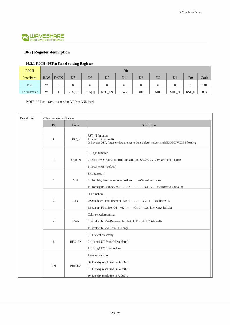
10.2.1 R00H (PSR): Panel setting Register
R00H Bit
Inst/Para R/W D/CX D7 D6 D5 D4 D3 D2 D1 D0 Code
PSR W 0 0 0 0 0 0 0 0 0 00H
1st Parameter W 1 RES[1] RES[0] REG_EN BWR UD SHL SHD_N RST_N 8Fh
NOTE: “-” Don’t care, can be set to VDD or GND level
Description -The command defines as :
Bit Name Description
0 RST_N RST_N function 1 : no effect. (default) 0: Booster OFF, Register data are set to their default values, and SEG/BG/VCOM:floating
1 SHD_N
SHD_N function
0 : Booster OFF, register data are kept, and SEG/BG/VCOM are kept floating.
1 : Booster on. (default)
2 SHL
SHL function
0: Shift left; First data=Sn →Sn-1 →…→S2 →Last data=S1.
1: Shift right: First data=S1→S2 →…→Sn-1 →Last data=Sn. (default)
3 UD
UD function
0:Scan down; First line=Gn→Gn-1 →…→G2 →Last line=G1.
1:Scan up; First line=G1 →G2 →…→Gn-1 →Last line=Gn. (default)
4 BWR
Color selection setting
0: Pixel with B/W/Reserve. Run both LU1 and LU2. (default)
1: Pixel with B/W. Run LU1 only
5 REG_EN
LUT selection setting
0 : Using LUT from OTP(default)
1 : Using LUT from register
7-6 RES[1,0]
Resolution setting
00: Display resolution is 600x448
01: Display resolution is 640x480
10: Display resolution is 720x540
3.7inch e-Paper
PAGE 25
11: Display resolution is 800x600 (default)
Notes:
1. When SHD_N become low, DCDC will turn off. Register and SRAM data will keep until VDD turn off. SD output and VCOM will base
on previous condition and keep floating.
2. When RST_N become low, driver will reset. All register will reset to default value. All of the driver’s functions will disable. SD output
and VCOM will base on previous condition and keep floating.
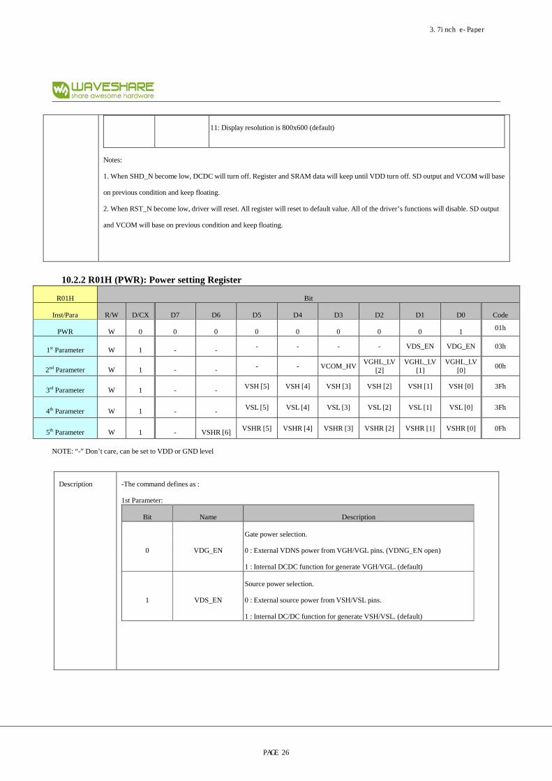
10.2.2 R01H (PWR): Power setting Register
R01H Bit
Inst/Para R/W D/CX D7 D6 D5 D4 D3 D2 D1 D0 Code
PWR W 0 0 0 0 0 0 0 0 1 01h
1st Parameter W 1 - - - - - - VDS_EN VDG_EN 03h
2nd Parameter W 1 - - - - VCOM_HV VGHL_LV
[2] VGHL_LV
[1] VGHL_LV
[0] 00h
3rd Parameter W 1 - - VSH [5] VSH [4] VSH [3] VSH [2] VSH [1] VSH [0] 3Fh
4th Parameter W 1 - - VSL [5] VSL [4] VSL [3] VSL [2] VSL [1] VSL [0] 3Fh
5th Parameter W 1 - VSHR [6] VSHR [5] VSHR [4] VSHR [3] VSHR [2] VSHR [1] VSHR [0] 0Fh
NOTE: “-” Don’t care, can be set to VDD or GND level
Description -The command defines as :
1st Parameter:
Bit Name Description
0 VDG_EN
Gate power selection.
0 : External VDNS power from VGH/VGL pins. (VDNG_EN open)
1 : Internal DCDC function for generate VGH/VGL. (default)
1 VDS_EN
Source power selection.
0 : External source power from VSH/VSL pins.
1 : Internal DC/DC function for generate VSH/VSL. (default)
3.7inch e-Paper
PAGE 26

2nd Parameter:
Bit Name Description
2-0 VGHL_LV
VGHL_LV Voltage Level.
000: VGH=20 v, VGL=-20v (default)
001: VGH=19 v, VGL=-19v
010: VGH=18 v, VGL=-18v
011: VGH=17 v, VGL=-17v
100: VGH=16 v, VGL=-16v
101: VGH=15 v, VGL=-15v
110: VGH=14 v, VGL=-14v
111: VGH=13 v, VGL=-13v
3 VCOM_HV
VCOM Voltage Level
0: VCOMH=VSH+VCOMDC,VCOML=VSL+VCOMDC(default)
1: VCOMH=VGH, VCOML=VGL
3rd Parameter: Internal VSH power selection for B/W LUT. (Default value: 111111b)
Bit Name Description
5-0 VSH
Internal VSH power selection.
000000: 2.4 v
000001: 2.6 v
000010: 2.8 v
000011: 3.0 v
….
010111: 7.0V
011000: 7.2 V
011001: 7.4 V
….
111010: 14.0V
111011: 14.2 V
111100: 14.4V
111101: 14.6V
111110: 14.8V
111111: 15.0V
3.7inch e-Paper
PAGE 27
4th Parameter: Internal VSL power selection for B/W LUT. (Default value: 111111b)
Bit Name Description
5-0 VSL
Internal VSL power selection.
000000: -2.4 v
000001: -2.6 v
000010: -2.8 v
000011: -3.0 v
….
010111: -7.0V
011000: -7.2 V
011001: -7.4 V
….
111010 :-14.0V
111011: -14.2 V
111100: -14.4 V
111101: -14.6V
111110: -14.8V
111111: -15.0V
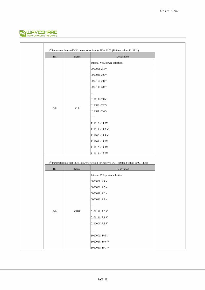
5th Parameter: Internal VSHR power selection for Reserve LUT. (Default value: 00001111b)
Bit Name Description
6-0 VSHR
Internal VSL power selection.
0000000: 2.4 v
0000001: 2.5 v
0000010: 2.6 v
0000011: 2.7 v
….
0101110: 7.0 V
0101111: 7.1 V
0110000: 7.2 V
….
1010001: 10.5V
1010010: 10.6 V
1010011: 10.7 V
3.7inch e-Paper
PAGE 28
1010100: 10.8V
1010101: 10.9V
1010110: 11.0V
Note:
1.VSH>VSHR
Restriction
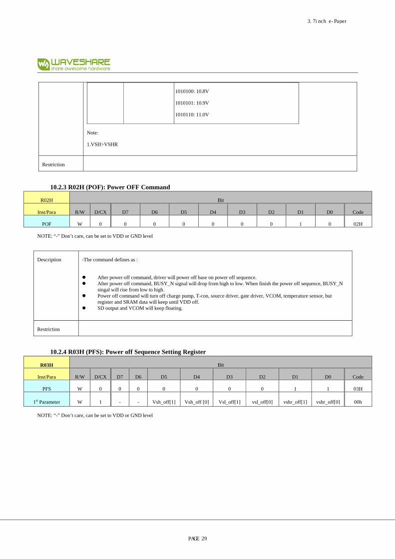
10.2.3 R02H (POF): Power OFF Command
R02H Bit
Inst/Para R/W D/CX D7 D6 D5 D4 D3 D2 D1 D0 Code
POF W 0 0 0 0 0 0 0 1 0 02H
NOTE: “-” Don’t care, can be set to VDD or GND level
Description -The command defines as :
� After power off command, driver will power off base on power off sequence. � After power off command, BUSY_N signal will drop from high to low. When finish the power off sequence, BUSY_N
singal will rise from low to high. � Power off command will turn off charge pump, T-con, source driver, gate driver, VCOM, temperature sensor, but
register and SRAM data will keep until VDD off. � SD output and VCOM will keep floating.
Restriction
10.2.4 R03H (PFS): Power off Sequence Setting Register
R03H Bit
Inst/Para R/W D/CX D7 D6 D5 D4 D3 D2 D1 D0 Code
PFS W 0 0 0 0 0 0 0 1 1 03H
1st Parameter W 1 - - Vsh_off[1] Vsh_off [0] Vsl_off[1] vsl_off[0] vshr_off[1] vshr_off[0] 00h
NOTE: “-” Don’t care, can be set to VDD or GND level
3.7inch e-Paper
PAGE 29

Description -The command defines as :
1st Parameter:
Bit Name Description
1-0 vshr_off
00: 5ms. (default)
01: 10ms
10: 20ms
11: 40ms
3-2 vsl_off
00: 5ms. (default)
01: 10ms
10: 20ms
11: 40ms
5-4 vsh_off
00: 5ms. (default)
01: 10ms
10: 20ms
11: 40ms
Restriction
10.2.5 R04H (PON): Power ON Command
R04H Bit
Inst/Para R/W D/CX D7 D6 D5 D4 D3 D2 D1 D0 Code
PON W 0 0 0 0 0 0 1 0 0 04H
NOTE: “-” Don’t care, can be set to VDD or GND level
Description -The command defines as :
� After power on command, driver will power on base on power on sequence. � After power on command, BUSY_N signal will drop from high to low. When finishing the power off sequence,
BUSY_N signal will rise from low to high.
Restriction
3.7inch e-Paper
PAGE 30
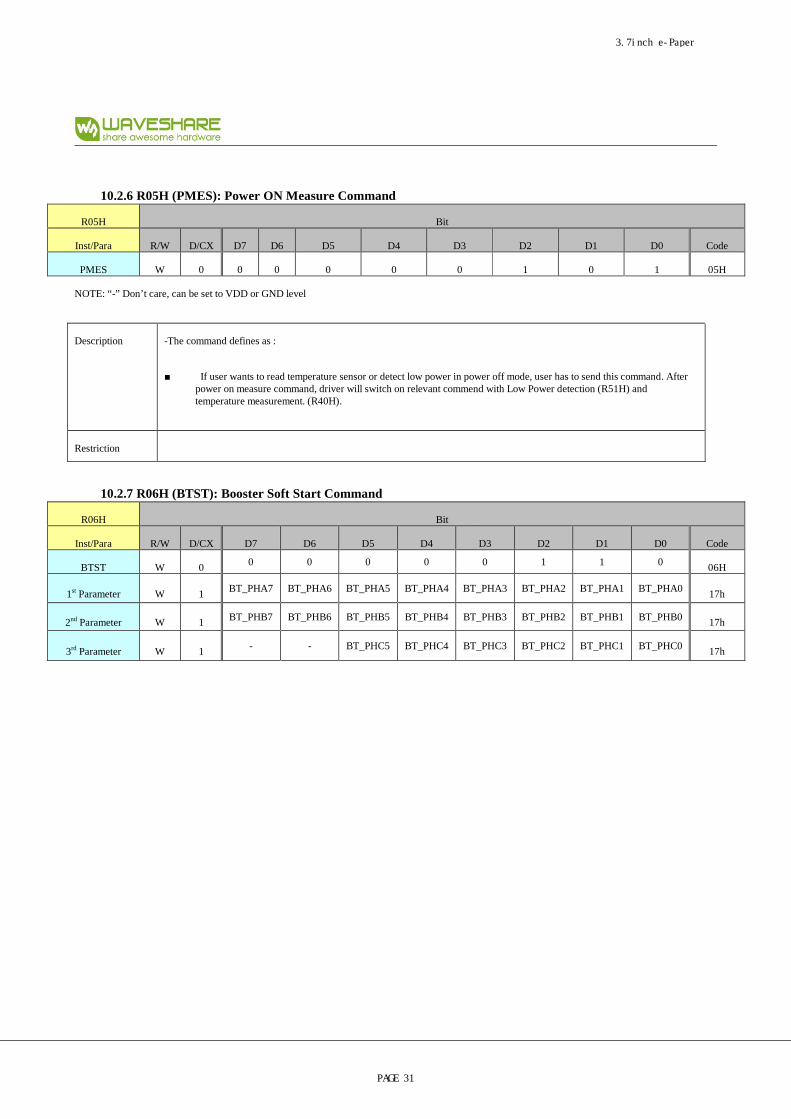
10.2.6 R05H (PMES): Power ON Measure Command
R05H Bit
Inst/Para R/W D/CX D7 D6 D5 D4 D3 D2 D1 D0 Code
PMES W 0 0 0 0 0 0 1 0 1 05H
NOTE: “-” Don’t care, can be set to VDD or GND level
Description -The command defines as :
■ If user wants to read temperature sensor or detect low power in power off mode, user has to send this command. Afterpower on measure command, driver will switch on relevant commend with Low Power detection (R51H) and temperature measurement. (R40H).
Restriction
10.2.7 R06H (BTST): Booster Soft Start Command
R06H Bit
Inst/Para R/W D/CX D7 D6 D5 D4 D3 D2 D1 D0 Code
BTST W 0 0 0 0 0 0 1 1 0 06H
1st Parameter W 1 BT_PHA7 BT_PHA6 BT_PHA5 BT_PHA4 BT_PHA3 BT_PHA2 BT_PHA1 BT_PHA0 17h
2nd Parameter W 1 BT_PHB7 BT_PHB6 BT_PHB5 BT_PHB4 BT_PHB3 BT_PHB2 BT_PHB1 BT_PHB0 17h
3rd Parameter W 1 - - BT_PHC5 BT_PHC4 BT_PHC3 BT_PHC2 BT_PHC1 BT_PHC0 17h
3.7inch e-Paper
PAGE 31

Description
-The command define as follows:
1st Parameter:
Bit Name Description
2-0
Driving strength of
phase A
000: period1
001: period2
010: period3
011: period4
100: period5
101: period6
110: period7
111: period8
5-3
000: Strength 1
001: Strength 2
010: Strength 3 (default)
011: Strength 4
100: Strength 5
101: Strength 6
110: Strength 7
111: Strength 8
7-6 Soft start period of
phase A
00: 10mS (default)
01: 20mS
10: 30mS
11: 40mS
3.7inch e-Paper
PAGE 32
Description
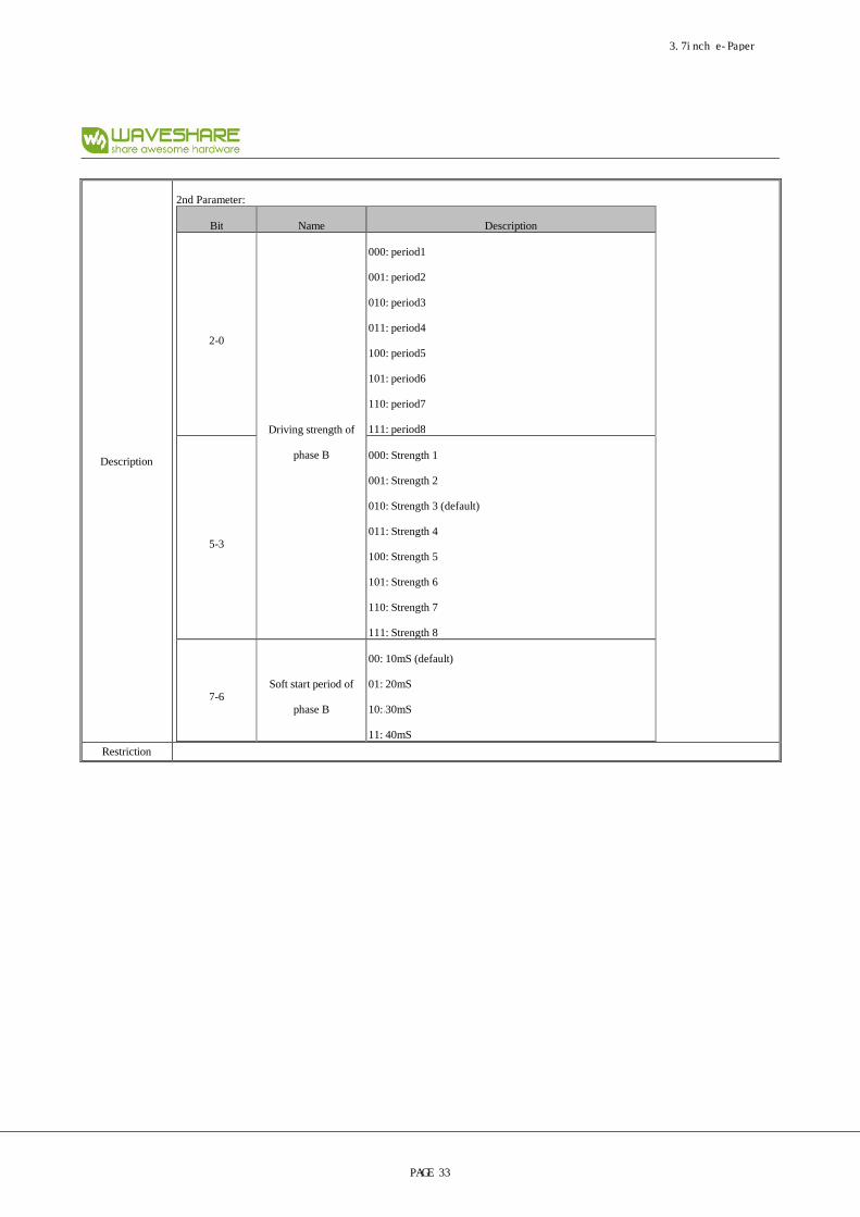
2nd Parameter:
Bit Name Description
2-0
Driving strength of
phase B
000: period1
001: period2
010: period3
011: period4
100: period5
101: period6
110: period7
111: period8
5-3
000: Strength 1
001: Strength 2
010: Strength 3 (default)
011: Strength 4
100: Strength 5
101: Strength 6
110: Strength 7
111: Strength 8
7-6 Soft start period of
phase B
00: 10mS (default)
01: 20mS
10: 30mS
11: 40mS
Restriction
3.7inch e-Paper
PAGE 33
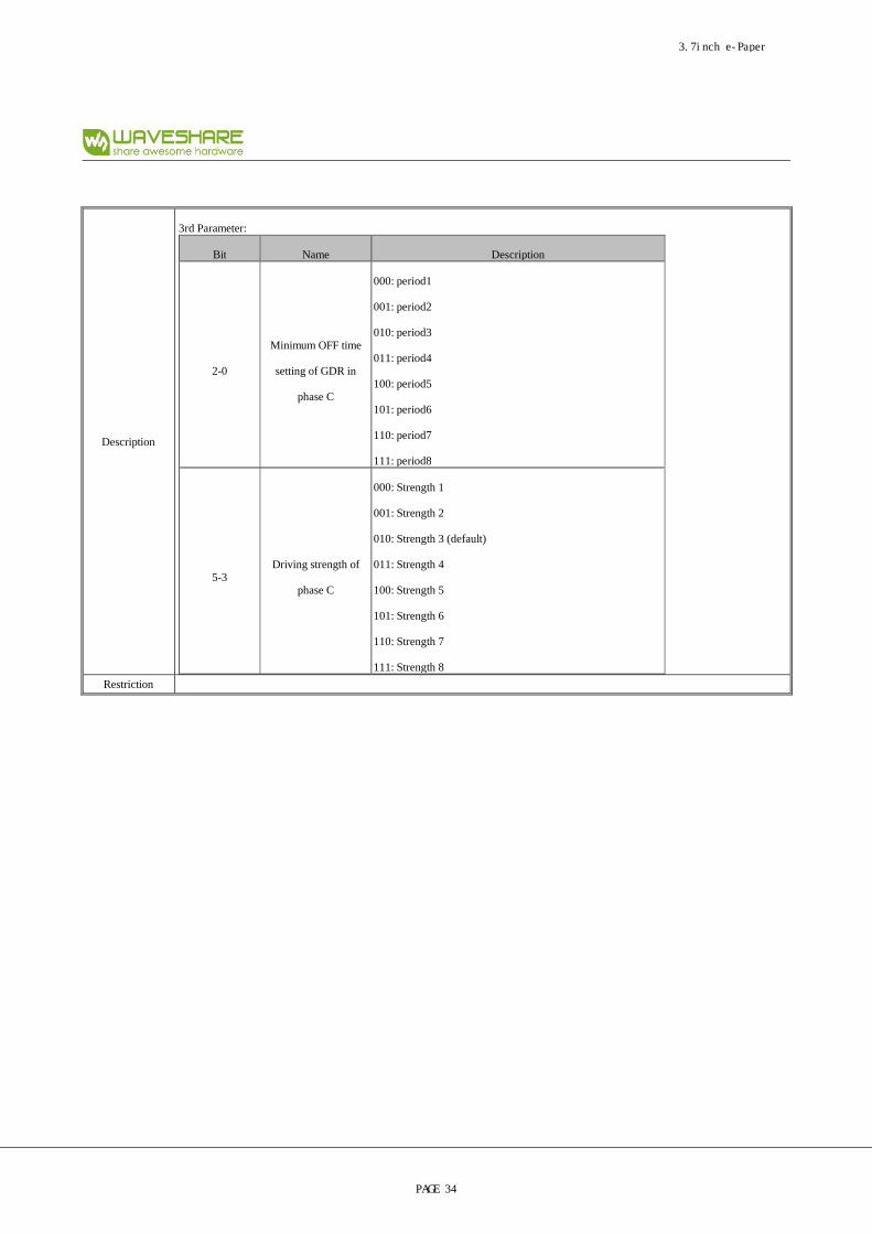
Description
3rd Parameter:
Bit Name Description
2-0
Minimum OFF time
setting of GDR in
phase C
000: period1
001: period2
010: period3
011: period4
100: period5
101: period6
110: period7
111: period8
5-3 Driving strength of
phase C
000: Strength 1
001: Strength 2
010: Strength 3 (default)
011: Strength 4
100: Strength 5
101: Strength 6
110: Strength 7
111: Strength 8
Restriction
3.7inch e-Paper
PAGE 34
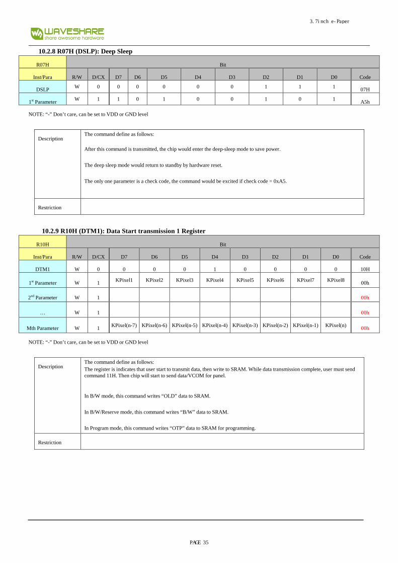
10.2.8 R07H (DSLP): Deep Sleep
R07H Bit
Inst/Para R/W D/CX D7 D6 D5 D4 D3 D2 D1 D0 Code
DSLP W 0 0 0 0 0 0 1 1 1 07H
1st Parameter W 1 1 0 1 0 0 1 0 1 A5h
NOTE: “-” Don’t care, can be set to VDD or GND level
Description The command define as follows:
After this command is transmitted, the chip would enter the deep-sleep mode to save power.
The deep sleep mode would return to standby by hardware reset.
The only one parameter is a check code, the command would be excited if check code = 0xA5.
Restriction
10.2.9 R10H (DTM1): Data Start transmission 1 Register
R10H Bit
Inst/Para R/W D/CX D7 D6 D5 D4 D3 D2 D1 D0 Code
DTM1 W 0 0 0 0 1 0 0 0 0 10H
1st Parameter W 1 KPixel1 KPixel2 KPixel3 KPixel4 KPixel5 KPixel6 KPixel7 KPixel8 00h
2nd Parameter W 1 00h
… W 1 00h
Mth Parameter W 1 KPixel(n-7) KPixel(n-6) KPixel(n-5) KPixel(n-4) KPixel(n-3) KPixel(n-2) KPixel(n-1) KPixel(n) 00h
NOTE: “-” Don’t care, can be set to VDD or GND level
Description The command define as follows: The register is indicates that user start to transmit data, then write to SRAM. While data transmission complete, user must send command 11H. Then chip will start to send data/VCOM for panel.
In B/W mode, this command writes “OLD” data to SRAM.
In B/W/Reserve mode, this command writes “B/W” data to SRAM.
In Program mode, this command writes “OTP” data to SRAM for programming.
Restriction
3.7inch e-Paper
PAGE 35
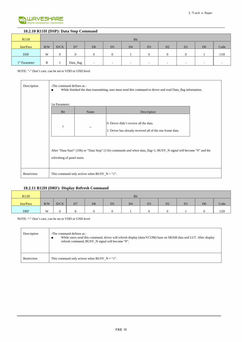
10.2.10 R11H (DSP): Data Stop Command
R11H Bit
Inst/Para R/W D/CX D7 D6 D5 D4 D3 D2 D1 D0 Code
DSP W 0 0 0 0 1 0 0 0 1 11H
1st Parameter R 1 Data_flag - - - - - - - -
NOTE: “-” Don’t care, can be set to VDD or GND level
Description -The command defines as : ■ While finished the data transmitting, user must send this command to driver and read Data_flag information.
1st Parameter:
Bit Name Description
7 -- 0: Driver didn’t receive all the data.
1: Driver has already received all of the one frame data.
After “Data Start” (10h) or “Data Stop” (11h) commands and when data_flag=1, BUSY_N signal will become “0” and the
refreshing of panel starts.
Restriction This command only actives when BUSY_N = “1”.
10.2.11 R12H (DRF): Display Refresh Command
R12H Bit
Inst/Para R/W D/CX D7 D6 D5 D4 D3 D2 D1 D0 Code
DRF W 0 0 0 0 1 0 0 1 0 12H
NOTE: “-” Don’t care, can be set to VDD or GND level
Description -The command defines as : ■ While users send this command, driver will refresh display (data/VCOM) base on SRAM data and LUT. After display
refresh command, BUSY_N signal will become “0”.
Restriction This command only actives when BUSY_N = “1”.
3.7inch e-Paper
PAGE 36

10.2.12 R13H (DTM2): Data Start transmission 2 Register
R13H Bit
Inst/Para R/W D/CX D7 D6 D5 D4 D3 D2 D1 D0 Code
DTM2 W 0 0 0 0 1 0 0 1 1 13H
1st Parameter W 1 KPixel1 KPixel2 KPixel3 KPixel4 KPixel5 KPixel6 KPixel7 KPixel8 00h
2nd Parameter W 1 00h
… W 1 00h
Mth Parameter W 1 KPixel(n-7) KPixel(n-6) KPixel(n-5) KPixel(n-4) KPixel(n-3) KPixel(n-2) KPixel(n-1) KPixel(n) 00h
NOTE: “-” Don’t care, can be set to VDD or GND level
Description The command define as follows: The register is indicates that user start to transmit data, then write to SRAM. While data transmission complete, user must send command 11H. Then chip will start to send data/VCOM for panel.
In B/W mode, this command writes “NEW” data to SRAM.
In B/W/Reserve mode, this command writes “RESERVE” data to SRAM.
Restriction
10.2.13 R14H (PDTM1): Partial Data Start transmission 1 Register
R14H Bit
Inst/Para R/W D/CX D7 D6 D5 D4 D3 D2 D1 D0 Code
PDTM1 W 0 0 0 0 1 0 1 0 0 14H
1st Parameter X[9] X[8 ]
2nd Parameter W 1 X[7] X[6] X[5] X[4] X[3] 0 0 0 00h
3rd Parameter Y[9] Y[8 ] 00h
4th Parameter W 1 Y[7] Y[6] Y[5] Y[4] Y[3] Y[2] Y[1] Y[0] 00h
5th Parameter W[9] W[8]
6th Parameter W 1 W[7] W[6] W[5] W[4] W[3] 0 0 0 00h
7th Parameter L[9] L[8 ] 00h
8th Parameter W 1 L[7] L[6] L[5] L[4] L[3] L[2] L[1] L[0] 00h
9th Parameter W 1 KPixel1 KPixel2 KPixel3 KPixel4 KPixel5 KPixel6 KPixel7 KPixel8 00h
W 1 00h
M th Parameter W 1 KPixel(n-7) KPixel(n-6) KPixel(n-5) KPixel(n-4) KPixel(n-3) KPixel(n-2) KPixel(n-1) KPixel(n) 00h
NOTE: “-” Don’t care, can be set to VDD or GND level
3.7inch e-Paper
PAGE 37
Description The command define as follows: The register is indicates that user start to transmit data, then write to SRAM. While data transmission complete, user must send command 11H. Then chip will start to send data/VCOM for panel.
In B/W mode, this command writes “OLD” data to SRAM.
In B/W/Reserve mode, this command writes “B/W” data to SRAM.
Partial update location and area
Note: X and W should be the multiple of 8.
Restriction
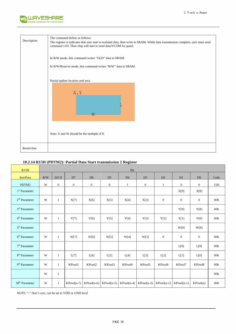
10.2.14 R15H (PDTM2): Partial Data Start transmission 2 Register
R15H Bit
Inst/Para R/W D/CX D7 D6 D5 D4 D3 D2 D1 D0 Code
PDTM2 W 0 0 0 0 1 0 1 0 0 15H
1st Parameter X[9] X[8]
2nd Parameter W 1 X[7] X[6] X[5] X[4] X[3] 0 0 0 00h
3rd Parameter Y[9] Y[8] 00h
4th Parameter W 1 Y[7] Y[6] Y[5] Y[4] Y[3] Y[2] Y[1] Y[0] 00h
5th Parameter W[9] W[8]
6th Parameter W 1 W[7] W[6] W[5] W[4] W[3] 0 0 0 00h
7th Parameter L[9] L[8] 00h
8th Parameter W 1 L[7] L[6] L[5] L[4] L[3] L[2] L[1] L[0] 00h
9th Parameter W 1 KPixel1 KPixel2 KPixel3 KPixel4 KPixel5 KPixel6 KPixel7 KPixel8 00h
W 1 00h
M th Parameter W 1 KPixel(n-7) KPixel(n-6) KPixel(n-5) KPixel(n-4) KPixel(n-3) KPixel(n-2) KPixel(n-1) KPixel(n) 00h
NOTE: “-” Don’t care, can be set to VDD or GND level
3.7inch e-Paper
PAGE 38

Description The command define as follows: The register is indicates that user start to transmit data, then write to SRAM. While data transmission complete, user must send command 11H. Then chip will start to send data/VCOM for panel.
In B/W mode, this command writes “NEW” data to SRAM.
In B/W/Reserve mode, this command writes “RESERVE” data to SRAM.
Partial update location and area
Note: X and W should be the multiple of 8.
Restriction
10.2.15 R16H (PDRF): Partial Display Refresh Command
R16H Bit
Inst/Para R/W D/CX D7 D6 D5 D4 D3 D2 D1 D0 Code
PDRF W 0 0 0 0 1 0 1 1 0 16H
1st Parameter W 1 DFV_EN X[9] X[8] 00h
2nd Parameter X[7] X [6] X[5] X[4] X[3] 0 0 0 00h
3rd Parameter W 1 Y[9] Y [8] 00h
4th Parameter W 1 Y[7] Y[6] Y[5] Y[4] Y[3] Y[2] Y[1] Y[0] 00h
5th Parameter W[9] W[8] 00h
6th Parameter W 1 W[7] W[6] W[5] W[4] W[3] 0 0 0 00h
7th Parameter L[9] L[8]
8th Parameter L[7] L[6] L[5] L[4] L[3] L[2] L[1] L[0]
NOTE: “-” Don’t care, can be set to VDD or GND level
Description -The command define as follows: While user sent this command, driver will refresh display (data/VCOM) base on SRAM data and LUT. Only the area (X,Y, W, L) would update, the others pixel output would follow VCOM LUT After display refresh command, BUSY_N signal will become “0”.
3.7inch e-Paper
PAGE 39

Note: X and W should be the multiple of 8.
DFV_EN: data follow VCOM function on display area. DFV_EN=1: Only effective in B/W mode, if pixel from “New data” SRAM equal to “Old data” SRAM on display area, this pixel output would follow VCOM LUT.
DFV_EN=0: Data doesn’t follow VCOM LUT.
Restriction This command only active when BUSY_N = “1”.
10.2.16 R20H (LUTC): LUT for Vcom
R20H Bit
Inst/Para R/W D/CX D7 D6 D5 D4 D3 D2 D1 D0 Code
LUTC W 0 0 0 1 0 0 0 0 0 20H
1st Parameter W 1 1st Level selection [1:0] 2nd Level selection [1:0] 3rd Level selection [1:0] 4th level selection[1:0] 00h
2nd Parameter W 1 1st Frame number [7:0] 00h
3rd Parameter W 1 2nd Frame number [7:0] 00h
4th Parameter W 1 3rd Frame number[7:0] 00h
5th Parameter W 1 4th Frame number[7:0] 00h
6th Parameter W 1 Repeat numbers[7:0] 00h
7th~13th Parameter W 1 2nd state 00h
…. W 1 3rd ~9th state 00h
55th ~60h Parameter W 1 10th state 00h
NOTE: “-” Don’t care, can be set to VDD or GND level
Description -The command defines as:
This register is set for VCOM LUT.
This command stores VCOM Look-Up Table with 10 states of data. Each group contains information for one state and is
storeserve with 6 bytes, while the sixth byte indicates how many times that phase will repeat.
If BWR=0 (BWR mode), User could choose 7~10 groups by R26H (SET_STG)
If BWR=1 (BW mode), only 7 groups are used.
define description
Level selection [1:0] 00: -VCM_DC
01: VSH+VCM_DC.
10: VSL+VCM_DC.
3.7inch e-Paper
PAGE 40
11: Floating.
Frame number [7:0] 00000000 :0 frame
00000001: 1 frame
…
11111110: 254 frame
11111111: 255 frame
Repeat numbers [7:0] 00000000 : 0
00000001: 1
…
11111110: 254
11111111: 255
Restriction This command only actives when BUSY_N = “1”.
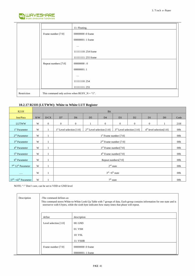
10.2.17 R21H (LUTWW): White to White LUT Register
R21H Bit
Inst/Para R/W D/CX D7 D6 D5 D4 D3 D2 D1 D0 Code
LUTWW W 0 0 0 1 0 0 0 0 1 21H
1st Parameter W 1 1st Level selection [1:0] 2nd Level selection [1:0] 3rd Level selection [1:0] 4th level selection[1:0] 00h
2nd Parameter W 1 1st Frame number [7:0] 00h
3rd Parameter W 1 2nd Frame number [7:0] 00h
4th Parameter W 1 3rd Frame number[7:0] 00h
5th Parameter W 1 4th Frame number[7:0] 00h
6th Parameter W 1 Repeat numbers[7:0] 00h
7th~12th Parameter W 1 2nd state 00h
…. W 1 3rd ~6th state 00h
37th ~42th Parameter W 1 7th state 00h
NOTE: “-” Don’t care, can be set to VDD or GND level
Description -The command defines as:
This command stores White-to-White Look-Up Table with 7 groups of data. Each group contains information for one state and is storeserve with 6 bytes, while the sixth byte indicates how many times that phase will repeat.
define description
Level selection [1:0] 00: GND
01: VSH
10: VSL
11: VSHR
Frame number [7:0] 00000000 :0 frame
00000001: 1 frame
3.7inch e-Paper
PAGE 41
.
11111110: 254 frame
11111111: 255 frame
Repeat numbers [7:0] 00000000 : 0 time
00000001: 1 time
.
11111110: 254 times
11111111: 255 times
Restriction This command only actives when BUSY_N = “1”.
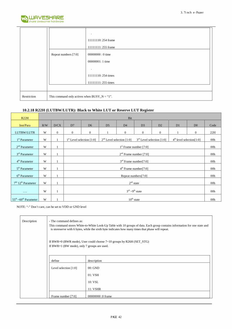
10.2.18 R22H (LUTBW/LUTR): Black to White LUT or Reserve LUT Register
R22H Bit
Inst/Para R/W D/CX D7 D6 D5 D4 D3 D2 D1 D0 Code
LUTBW/LUTR W 0 0 0 1 0 0 0 1 0 22H
1st Parameter W 1 1st Level selection [1:0] 2nd Level selection [1:0] 3rd Level selection [1:0] 4th level selection[1:0] 00h
2nd Parameter W 1 1st Frame number [7:0] 00h
3rd Parameter W 1 2nd Frame number [7:0] 00h
4th Parameter W 1 3rd Frame number[7:0] 00h
5th Parameter W 1 4th Frame number[7:0] 00h
6th Parameter W 1 Repeat numbers[7:0] 00h
7th~12th Parameter W 1 2nd state 00h
…. W 1 3rd ~9th state 00h
55th ~60th Parameter W 1 10th state 00h
NOTE: “-” Don’t care, can be set to VDD or GND level
Description - The command defines as:
This command stores White-to-White Look-Up Table with 10 groups of data. Each group contains information for one state and is storeserve with 6 bytes, while the sixth byte indicates how many times that phase will repeat.
If BWR=0 (BWR mode), User could choose 7~10 groups by R26H (SET_STG)
If BWR=1 (BW mode), only 7 groups are used.
define description
Level selection [1:0] 00: GND
01: VSH
10: VSL
11: VSHR
Frame number [7:0] 00000000 :0 frame
3.7inch e-Paper
PAGE 42
00000001: 1 frame
.
11111110: 254 frame
11111111: 255 frame
Repeat numbers [7:0] 00000000 : 0 time
00000001: 1 time
.
11111110: 254 times
11111111: 255 times
Restriction This command only actives when BUSY_N = “1”.
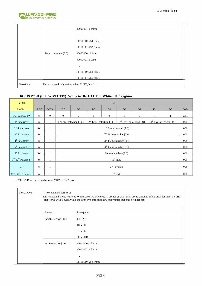
10.2.19 R23H (LUTWB/LUTW): White to Black LUT or White LUT Register
R23H Bit
Inst/Para R/W D/CX D7 D6 D5 D4 D3 D2 D1 D0 Code
LUTWB/LUTW W 0 0 0 1 0 0 0 1 1 23H
1st Parameter W 1 1st Level selection [1:0] 2nd Level selection [1:0] 3rd Level selection [1:0] 4th level selection[1:0] 00h
2nd Parameter W 1 1st Frame number [7:0] 00h
3rd Parameter W 1 2nd Frame number [7:0] 00h
4th Parameter W 1 3rd Frame number[7:0] 00h
5th Parameter W 1 4th Frame number[7:0] 00h
6th Parameter W 1 Repeat numbers[7:0] 00h
7th~12th Parameter W 1 2nd state 00h
…. W 1 3rd ~6th state 00h
37th ~42th Parameter W 1 7th state 00h
NOTE: “-” Don’t care, can be set to VDD or GND level
Description - The command defines as:
This command stores White-to-White Look-Up Table with 7 groups of data. Each group contains information for one state and is storeserve with 6 bytes, while the sixth byte indicates how many times that phase will repeat.
define description
Level selection [1:0] 00: GND
01: VSH
10: VSL
11: VSHR
Frame number [7:0] 00000000 :0 frame
00000001: 1 frame
.
11111110: 254 frame
3.7inch e-Paper
PAGE 43
11111111: 255 frame
Repeat numbers [7:0] 00000000 : 0 time
00000001: 1 time
.
11111110: 254 times
11111111: 255 times
Restriction This command only actives when BUSY_N = “1”.
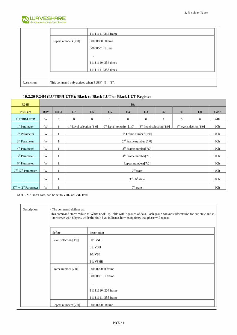
10.2.20 R24H (LUTBB/LUTB): Black to Black LUT or Black LUT Register
R24H Bit
Inst/Para R/W D/CX D7 D6 D5 D4 D3 D2 D1 D0 Code
LUTBB/LUTB W 0 0 0 1 0 0 1 0 0 24H
1st Parameter W 1 1st Level selection [1:0] 2nd Level selection [1:0] 3rd Level selection [1:0] 4th level selection[1:0] 00h
2nd Parameter W 1 1st Frame number [7:0] 00h
3rd Parameter W 1 2nd Frame number [7:0] 00h
4th Parameter W 1 3rd Frame number[7:0] 00h
5th Parameter W 1 4th Frame number[7:0] 00h
6th Parameter W 1 Repeat numbers[7:0] 00h
7th~12th Parameter W 1 2nd state 00h
…. W 1 3rd ~6th state 00h
37th ~42th Parameter W 1 7th state 00h
NOTE: “-” Don’t care, can be set to VDD or GND level
Description - The command defines as:
This command stores White-to-White Look-Up Table with 7 groups of data. Each group contains information for one state and is storeserve with 6 bytes, while the sixth byte indicates how many times that phase will repeat.
define description
Level selection [1:0] 00: GND
01: VSH
10: VSL
11: VSHR
Frame number [7:0] 00000000 :0 frame
00000001: 1 frame
.
11111110: 254 frame
11111111: 255 frame
Repeat numbers [7:0] 00000000 : 0 time
3.7inch e-Paper
PAGE 44

00000001: 1 time
.
11111110: 254 times
11111111: 255 times
Restriction This command only actives when BUSY_N = “1”.
10.2.21 R25H (LUTC Option): LUTC option
R25H Bit
Inst/Para R/W D/CX D7 D6 D5 D4 D3 D2 D1 D0 Code
LUTC option W 0 0 0 1 0 0 0 0 0 20H
1st Parameter W 1 XON [9:8] 00h
2nd Parameter W 1 XON [7:0] 00h
3rd Parameter W 1 VCOM_H [9:8] 00h
4th Parameter W 1 VCOM_H [7:0] 00h
NOTE: “-” Don’t care, can be set to VDD or GND level
Description -The command defines as:
This register is set for VCOM LUT.
XON[9:0] All Gate ON
0000000000: No all gate on.
0000000001: State1 gate power on
1111111111: State1~10 all gate power on
VCOM_H[9:0] Control VCOM Power as High
0000000000: No VCOM High voltage
0000000001: State1 VCOM High voltage
….
1111111111: State1~10 VCOM High voltage
3.7inch e-Paper
PAGE 45
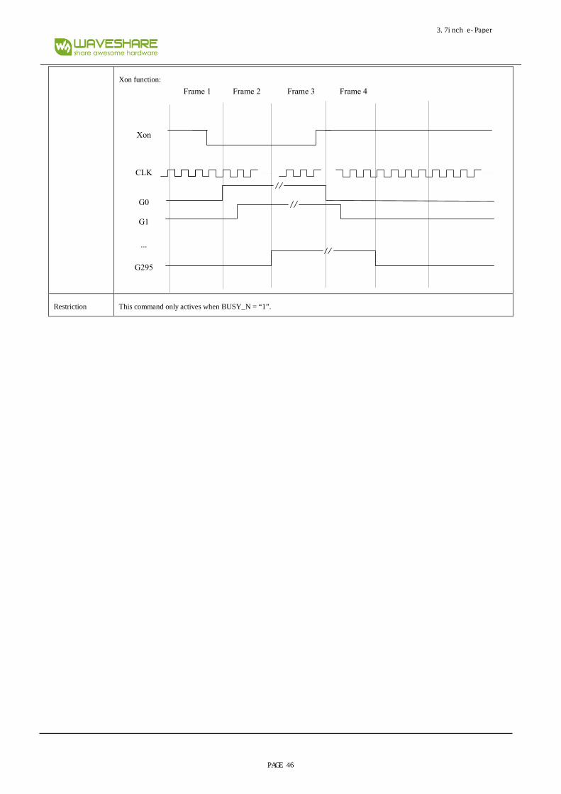
Xon function:
Xon
CLK
G0
Frame 1 Frame 2 Frame 3 Frame 4
G1
G295
...
Restriction This command only actives when BUSY_N = “1”.
3.7inch e-Paper
PAGE 46
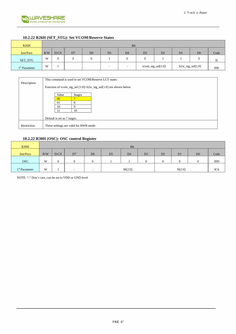
10.2.22 R26H (SET_STG): Set VCOM/Reserve States
R26H Bit
Inst/Para R/W D/CX D7 D6 D5 D4 D3 D2 D1 D0 Code
SET_STG W 0 0 0 1 0 0 1 1 0 H
1st Parameter W 1 - - vcom_stg_sel[1:0] b2w_stg_sel[1:0] 00h
Description This command is used to set VCOM/Reserve LUT states
Function of vcom_stg_sel [1:0]/ b2w_stg_sel[1:0] are shown below
Value Stages 00 7 01 8 10 9 11 10
Default is set as 7 stages.
Restriction These settings are valid for BWR mode.
10.2.22 R30H (OSC): OSC control Register
R30H Bit
Inst/Para R/W D/CX D7 D6 D5 D4 D3 D2 D1 D0 Code
OSC W 0 0 0 1 1 0 0 0 0 30H
1st Parameter W 1 - - M[2:0] N[2:0] 3Ch
NOTE: “-” Don’t care, can be set to VDD or GND level
3.7inch e-Paper
PAGE 47
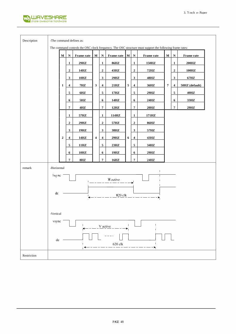
Description -The command defines as:
The command controls the OSC clock frequency. The OSC structure must support the following frame rates:
M N Frame rate M N Frame rate M N Frame rate M N Frame rate
1
1 29HZ
3
1 86HZ
5
1 150HZ
7
1 200HZ
2 14HZ 2 43HZ 2 72HZ 2 100HZ
3 10HZ 3 29HZ 3 48HZ 3 67HZ
4 7HZ 4 21HZ 4 36HZ 4 50HZ (default)
5 6HZ 5 17HZ 5 29HZ 5 40HZ
6 5HZ 6 14HZ 6 24HZ 6 33HZ
7 4HZ 7 12HZ 7 20HZ 7 29HZ
2
1 57HZ
4
1 114HZ
6
1 171HZ
2 29HZ 2 57HZ 2 86HZ
3 19HZ 3 38HZ 3 57HZ
4 14HZ 4 29HZ 4 43HZ
5 11HZ 5 23HZ 5 34HZ
6 10HZ 6 19HZ 6 29HZ
7 8HZ 7 16HZ 7 24HZ
remark -Horizental
-Vertical
vsync
de
V active
620 clk
Restriction
3.7inch e-Paper
PAGE 48
10.2.23 R40H (TSC): Temperature Sensor Command
R40H Bit
Inst/Para R/W D/CX D7 D6 D5 D4 D3 D2 D1 D0 Code
TSC W 0 0 1 0 0 0 0 0 0 40H
1st Parameter R 1 D10/TS[7] D9/TS[6] D8/TS[5] D7/TS[4] D6/TS[3] D5/TS[2] D4/TS[1] D3/TS[0] -
2nd Parameter R 1 D2 D1 D0 - - - - - -
NOTE: “-” Don’t care, can be set to VDD or GND level
Description -The command define as follows: This command indicates the temperature value.
If R41H(TSE) bit7 set to 0, this command reads internal temperature sensor value.
If R41H(TSE) bit7 set to 1, this command reads external (LM75) temperature sensor value
TS[7:0]/D[10:3] T (°C) TS[7:0]/D[10:3] T (°C) TS[7:0]/D[10:3] T (°C)
11100111 -25 00000000 0 00011001 25
11101000 -24 00000001 1 00011010 26
11101001 -23 00000010 2 00011011 27
11101010 -22 00000011 3 00011100 28
11101011 -21 00000100 4 00011101 29
11101100 -20 00000101 5 00011110 30
11101101 -19 00000110 6 00011111 31
11101110 -18 00000111 7 00100000 32
11101111 -17 00001000 8 00100001 33
11110000 -16 00001001 9 00100010 34
11110001 -15 00001010 10 00100011 35
11110010 -14 00001011 11 00100100 36
11110011 -13 00001100 12 00100101 37
11110100 -12 00001101 13 00100110 38
11110101 -11 00001110 14 00100111 39
11110110 -10 00001111 15 00101000 40
11110111 -9 00010000 16 00101001 41
11111000 -8 00010001 17 00101010 42
3.7inch e-Paper
PAGE 49

11111001 -7 00010010 18 00101011 43
11111010 -6 00010011 19 00101100 44
11111011 -5 00010100 20 00101101 45
11111100 -4 00010101 21 00101110 46
11111101 -3 00010110 22 00101111 47
11111110 -2 00010111 23 00110000 48
11111111 -1 00011000 24 00110001 49
Restriction This command only actives after R04H(PON) or R05H(PMES)
10.2.24 R41H (TSE): Temperature Sensor Calibration Register
R41H Bit
Inst/Para R/W D/CX D7 D6 D5 D4 D3 D2 D1 D0 Code
TSE W 0 0 1 0 0 0 0 0 1 41H
1st Parameter W 1 TSE - - - TO[3] TO[2] TO[1] TO[0] 00h
NOTE: “-” Don’t care, can be set to VDD or GND level
Description -The command defines as:
This command indicates the driver IC temperature sensor enable and calibration function.
Bit temperature
2-0 mean temperature offset value
000:0℃
001:1℃
010:2℃
….
111:7℃
3 Positive and negative value
0:”+”
1: ”-“
7 Internal temperature sensor enable
0: Internal temperature sensor enable.(default)
1: Internal temperature sensor disable, using external temperature sensor.
For example:
1100: - 4 degree c
0111: + 7 degree c
Restriction This command only actives after R04H(PON) or R05H(PMES)
3.7inch e-Paper
PAGE 50

10.2.25 R42H (TSW): Temperature Sensor Write Register
R42H Bit
Inst/Para R/W D/CX D7 D6 D5 D4 D3 D2 D1 D0 Code
TSW W 0 0 1 0 0 0 0 1 0 42H
1st Parameter W 1 WATTR[7] WATTR[6] WATTR[5] WATTR[4] WATTR[3] WATTR[2] WATTR[1] WATTR[0] 00h
2nd Parameter W 1 WMSB[7] WMSB[6] WMSB[5] WMSB[4] WMSB[3] WMSB[2] WMSB[1] WMSB[0] 00h
3rd Parameter W 1 WLSB[7] WLSB[6] WLSB[5] WLSB[4] WLSB[3] WLSB[2] WLSB[1] WLSB[0] 00h
NOTE: “-” Don’t care, can be set to VDD or GND level
Description -The command defines as:
This command writes the temperature.
1st Parameter:
Bit temperature
2-0 Pointer setting
5-3 User-defined address bits (A2, A1, A0)
7-6 I2C Write Byte Number
00: 1 byte (head byte only)
01: 2 bytes (head byte + pointer)
10: 3 bytes (head byte + pointer + 1st parameter)
11: 4 bytes (head byte + pointer + 1st parameter + 2nd parameter)
2nd Parameter:
Bit temperature
7-0 MSByte of write-data to external temperature sensor
3nd Parameter:
Bit temperature
7-0 LSByte of write-data to external temperature sensor
Restriction This command only actives after R04H(PON) or R05H(PMES)
3.7inch e-Paper
PAGE 51
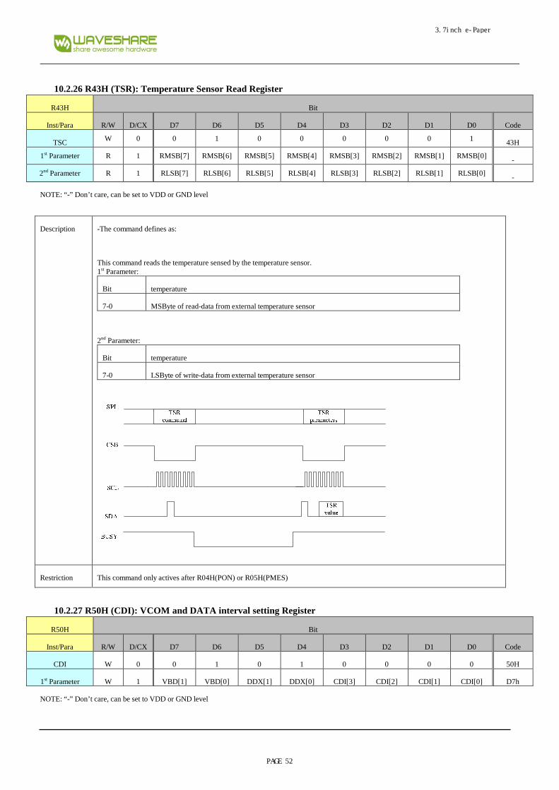
10.2.26 R43H (TSR): Temperature Sensor Read Register
R43H Bit
Inst/Para R/W D/CX D7 D6 D5 D4 D3 D2 D1 D0 Code
TSC W 0 0 1 0 0 0 0 0 1 43H
1st Parameter R 1 RMSB[7] RMSB[6] RMSB[5] RMSB[4] RMSB[3] RMSB[2] RMSB[1] RMSB[0] -
2nd Parameter R 1 RLSB[7] RLSB[6] RLSB[5] RLSB[4] RLSB[3] RLSB[2] RLSB[1] RLSB[0] -
NOTE: “-” Don’t care, can be set to VDD or GND level
Description -The command defines as:
This command reads the temperature sensed by the temperature sensor. 1st Parameter:
Bit temperature
7-0 MSByte of read-data from external temperature sensor
2nd Parameter:
Bit temperature
7-0 LSByte of write-data from external temperature sensor
Restriction This command only actives after R04H(PON) or R05H(PMES)
10.2.27 R50H (CDI): VCOM and DATA interval setting Register
R50H Bit
Inst/Para R/W D/CX D7 D6 D5 D4 D3 D2 D1 D0 Code
CDI W 0 0 1 0 1 0 0 0 0 50H
1st Parameter W 1 VBD[1] VBD[0] DDX[1] DDX[0] CDI[3] CDI[2] CDI[1] CDI[0] D7h
NOTE: “-” Don’t care, can be set to VDD or GND level
3.7inch e-Paper
PAGE 52
Description -The command defines as:
1st Parameter:
CDI[1:0]: This command indicates the interval of VCOM and data output. When setting the vertical back porch, the total blanking
will be keep (20hsync).
Bit
3-0 Vcom and data interval
0000: 17 hsync
0001:16 hsync
0010:15 hsync
0011:14 hsync
0100:13 hsync
0101:12 hsync
0110:11 hsync
0111:10 hsync
1000:9 hsync
1001:8 hsync
1010:7 hsync
1011:6 hsync
1100:5 hsync
1101:4 hsync
1110:3 hsync
1111:2 hsync
VBD[1:0] Border data selection.
B/W/Reserve mode(BWR=0)
Bit 5-4 Bit7-6 Description
DDX[0] VBD[1:0] LUT
0 00 Floating
3.7inch e-Paper
PAGE 53

01 LUTR
10 LUTW
11 LUTB
1 (default) 00 LUTB
01 LUTW
10 LUTR
11 (default) Floating
B/W mode (BWR=1)
Bit 5-4 Bit7-6 description
DDX[0] VBD[1:0] LUT
0 00 Floating
01 LUTBW (1->0)
10 LUTWB (0->1)
11 Floating
1 (default) 00 Floating
01 LUTWB (1->0)
10 LUTBW (0->1)
11 Floating
DDX[1:0]: Data polarity 1. DDX[1] for RESERVE data, DDX[0] for BW data in the B/W/Reserve mode2. DDX[0] for B/W mode
B/W/Reserve mode(BWR=0)
Bit 5-4 Description
DDX[1:0] Data (Reserve/B/W) LUT
00 00 LUTW
01 LUTB
10 LUTR
11 LUTR
01 (default) 00 LUTB
01 LUTW
10 LUTR
11 LUTR
10 00 LUTR
01 LUTR
10 LUTW
11 LUTB
3.7inch e-Paper
PAGE 54

11 00 LUTR
01 LUTR
10 LUTB
11 LUTW
B/W mode (BWR=1)
Bit 5-4 Description
DDX[0] Data (B/W) LUT
0 00 LUTWW (0->0)
01 LUTBW(1->0)
10 LUTWB(0->1)
11 LUTBB(1->1)
1 (default) 00 LUTBB(0->0)
01 LUTWB(1->0)
10 LUTBW(0->1)
11 LUTWW(1->1)
10.2.28 R51H (LPD): Lower Power Detection Register
R51H Bit
Inst/Para R/W D/CX D7 D6 D5 D4 D3 D2 D1 D0 Code
LPD W 0 0 1 0 1 0 0 0 1 51H
1st Parameter R 1 - - - - - - - LPD --
NOTE: “-” Don’t care, can be set to VDD or GND level
Description -The command defines as:
This command indicates the input power condition. Host can read this data to understand the battery’s condition.
When LPD=”1”, system input power is normal.
When LPD=”0”, system input power is lower (VDD<2.5v, which could be select in RE6H (LVSEL)).
1st Parameter:
Bit 0 LPD
0 Low power input.
1 Normal status.
Restriction
3.7inch e-Paper
PAGE 55
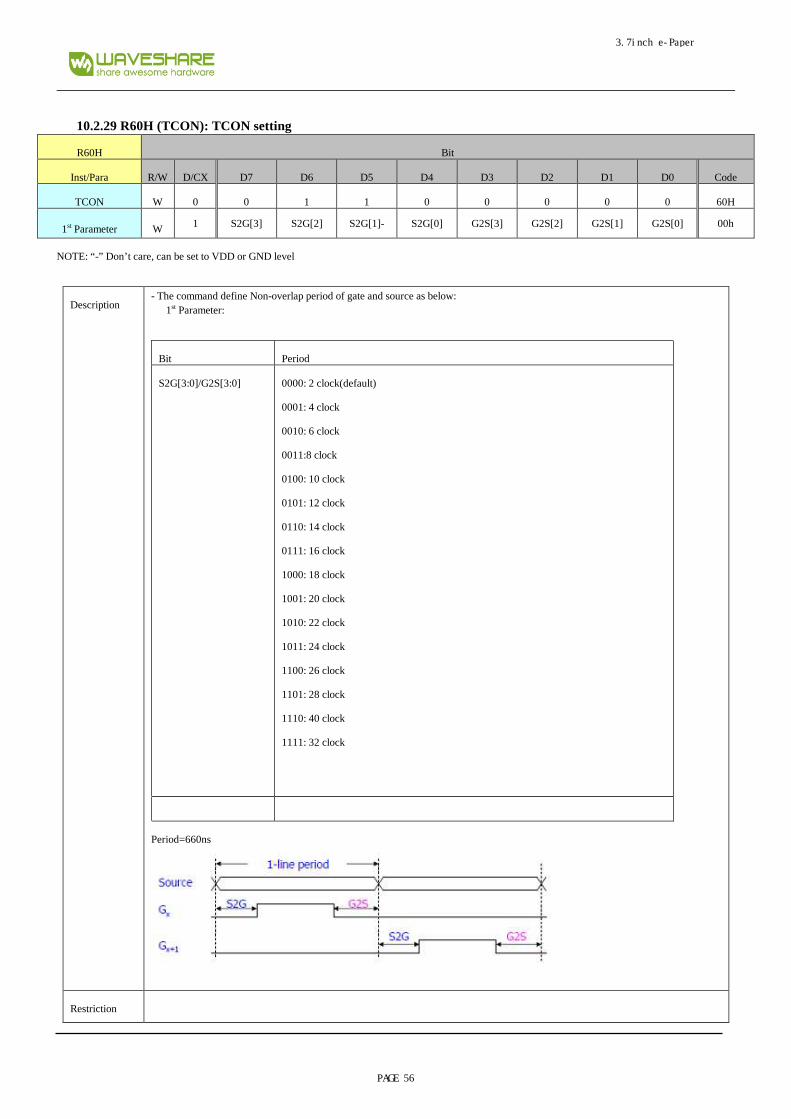
10.2.29 R60H (TCON): TCON setting
R60H Bit
Inst/Para R/W D/CX D7 D6 D5 D4 D3 D2 D1 D0 Code
TCON W 0 0 1 1 0 0 0 0 0 60H
1st Parameter W 1 S2G[3] S2G[2] S2G[1]- S2G[0] G2S[3] G2S[2] G2S[1] G2S[0] 00h
NOTE: “-” Don’t care, can be set to VDD or GND level
Description - The command define Non-overlap period of gate and source as below:
1st Parameter:
Bit Period
S2G[3:0]/G2S[3:0] 0000: 2 clock(default)
0001: 4 clock
0010: 6 clock
0011:8 clock
0100: 10 clock
0101: 12 clock
0110: 14 clock
0111: 16 clock
1000: 18 clock
1001: 20 clock
1010: 22 clock
1011: 24 clock
1100: 26 clock
1101: 28 clock
1110: 40 clock
1111: 32 clock
Period=660ns
Restriction
3.7inch e-Paper
PAGE 56
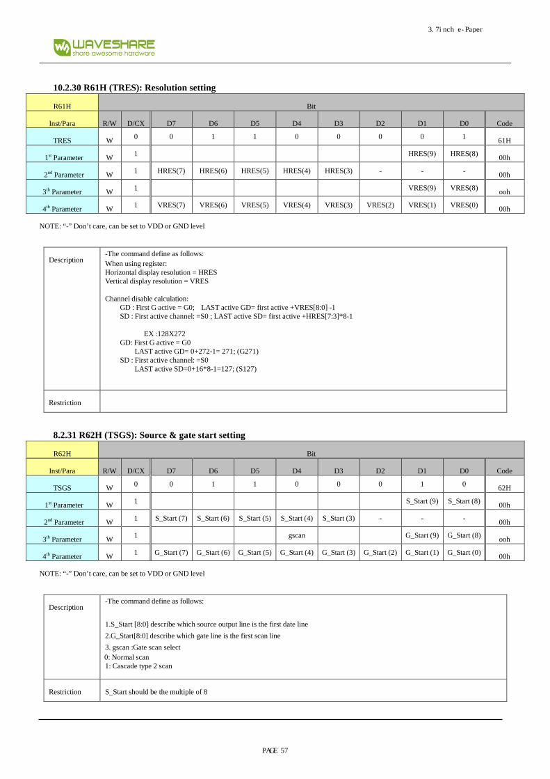
10.2.30 R61H (TRES): Resolution setting
R61H Bit
Inst/Para R/W D/CX D7 D6 D5 D4 D3 D2 D1 D0 Code
TRES W 0 0 1 1 0 0 0 0 1 61H
1st Parameter W 1 HRES(9) HRES(8) 00h
2nd Parameter W 1 HRES(7) HRES(6) HRES(5) HRES(4) HRES(3) - - - 00h
3th Parameter W 1 VRES(9) VRES(8) ooh
4th Parameter W 1 VRES(7) VRES(6) VRES(5) VRES(4) VRES(3) VRES(2) VRES(1) VRES(0) 00h
NOTE: “-” Don’t care, can be set to VDD or GND level
Description -The command define as follows: When using register: Horizontal display resolution = HRES Vertical display resolution = VRES
Channel disable calculation: GD : First G active = G0; LAST active GD= first active +VRES[8:0] -1 SD : First active channel: =S0 ; LAST active SD= first active +HRES[7:3]*8-1
EX :128X272 GD: First G active = G0
LAST active GD= 0+272-1= 271; (G271) SD : First active channel: =S0
LAST active SD=0+16*8-1=127; (S127)
Restriction
8.2.31 R62H (TSGS): Source & gate start setting
R62H Bit
Inst/Para R/W D/CX D7 D6 D5 D4 D3 D2 D1 D0 Code
TSGS W 0 0 1 1 0 0 0 1 0 62H
1st Parameter W 1 S_Start (9) S_Start (8) 00h
2nd Parameter W 1 S_Start (7) S_Start (6) S_Start (5) S_Start (4) S_Start (3) - - - 00h
3th Parameter W 1 gscan G_Start (9) G_Start (8) ooh
4th Parameter W 1 G_Start (7) G_Start (6) G_Start (5) G_Start (4) G_Start (3) G_Start (2) G_Start (1) G_Start (0) 00h
NOTE: “-” Don’t care, can be set to VDD or GND level
Description -The command define as follows:
1.S_Start [8:0] describe which source output line is the first date line
2.G_Start[8:0] describe which gate line is the first scan line
3. gscan :Gate scan select 0: Normal scan 1: Cascade type 2 scan
Restriction S_Start should be the multiple of 8
3.7inch e-Paper
PAGE 57

10.2.32 R70H (REV): REVISION register
R70H Bit
Inst/Para R/W D/CX D7 D6 D5 D4 D3 D2 D1 D0 Code
REV W 0 0 1 1 1 0 0 0 0 70H
1st Parameter R 1 REV[7] REV[6] REV[5] REV[4] REV[3] REV[2] REV[1] REV[0] -
2nd Parameter R 1 REV[15] REV[14] REV[13] REV[12] REV[11] REV[10] REV[9] REV[8] -
NOTE: “-” Don’t care, can be set to VDD or GND level
Description -The command defines as:
The LUT_REV is read from OTP address = 0x001.& 0x002
Restriction This command only actives when BUSY_N = “1”.
10.2.33 R71H (FLG): Status register
R71H Bit
Inst/Para R/W D/CX D7 D6 D5 D4 D3 D2 D1 D0 Code
FLG W 0 0 1 1 0 0 0 1 71H
1st Parameter R 1 - I2C_ERR II2C_
BUSYN Data_flag PON POF BUSY_N -
NOTE: “-” Don’t care, can be set to VDD or GND level
Description -The command defines as:
This command indicates the IC status. Host can read this data to understand the IC status.
1st Parameter:
Bit Function
5 I2C master error status
4 I2C master busy status (low active)
3 Driver has already received one frame data
2 PON
0: Not in PON mode
1: In PON mode
1 POF
0: Not in POF mode(default)
1: In POF mode
0 Driver busy status(low active)
Restriction User can send this command in any time. It doesn’t have restriction of BUSY_N.
3.7inch e-Paper
PAGE 58
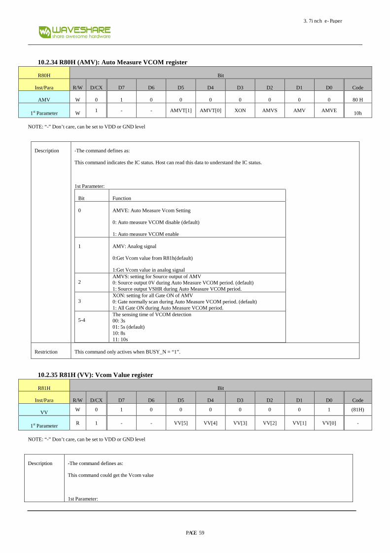
10.2.34 R80H (AMV): Auto Measure VCOM register
R80H Bit
Inst/Para R/W D/CX D7 D6 D5 D4 D3 D2 D1 D0 Code
AMV W 0 1 0 0 0 0 0 0 0 80 H
1st Parameter W 1 - - AMVT[1] AMVT[0] XON AMVS AMV AMVE 10h
NOTE: “-” Don’t care, can be set to VDD or GND level
Description -The command defines as:
This command indicates the IC status. Host can read this data to understand the IC status.
1st Parameter:
Bit Function
0 AMVE: Auto Measure Vcom Setting
0: Auto measure VCOM disable (default)
1: Auto measure VCOM enable
1 AMV: Analog signal
0:Get Vcom value from R81h(default)
1:Get Vcom value in analog signal
2 AMVS: setting for Source output of AMV 0: Source output 0V during Auto Measure VCOM period. (default) 1: Source output VSHR during Auto Measure VCOM period.
3 XON: setting for all Gate ON of AMV 0: Gate normally scan during Auto Measure VCOM period. (default) 1: All Gate ON during Auto Measure VCOM period.
5-4 The sensing time of VCOM detection 00: 3s 01: 5s (default) 10: 8s 11: 10s
Restriction This command only actives when BUSY_N = “1”.
10.2.35 R81H (VV): Vcom Value register
R81H Bit
Inst/Para R/W D/CX D7 D6 D5 D4 D3 D2 D1 D0 Code
VV W 0 1 0 0 0 0 0 0 1 (81H)
1st Parameter R 1 - - VV[5] VV[4] VV[3] VV[2] VV[1] VV[0] -
NOTE: “-” Don’t care, can be set to VDD or GND level
Description -The command defines as:
This command could get the Vcom value
1st Parameter:
3.7inch e-Paper
PAGE 59

Bit Function
5-0 Vcom value
000000: -0.1V
000001:-0.15V
000010:-0.2V
….
111000:-2.9V
111001:-2.95V
111010:-3.0V
Restriction This command only actives when BUSY_N = “1”.
10.2.36 R82H (VDCS): Vcom_DC Setting register
R82H Bit
Inst/Para R/W D/CX D7 D6 D5 D4 D3 D2 D1 D0 Code
VDCS W 0 1 0 0 0 0 0 1 0 82H
1st Parameter W 1 - - VCDS[5] VCDS [4] VCDS [3] VCDS [2] VCDS [1] VCDS [0] 1Fh
NOTE: “-” Don’t care, can be set to VDD or GND level
Description -The command defines as: This command set the VCOM DC value. Driver will base on this value for VCM_DC.
1st Parameter:
Bit Function
5-0 VCOM value
000000: -0.1V
000001:-0.15V
000010:-0.2V
….
111000:-2.9V
111001:-2.95V
111010:-3.0V
Restriction This command only actives when BUSY_N = “1”.
3.7inch e-Paper
PAGE 60
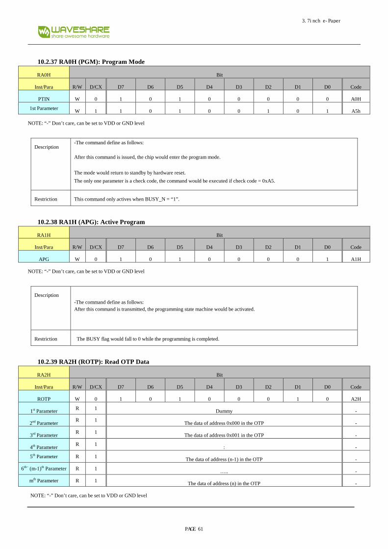
10.2.37 RA0H (PGM): Program Mode
RA0H Bit
Inst/Para R/W D/CX D7 D6 D5 D4 D3 D2 D1 D0 Code
PTIN W 0 1 0 1 0 0 0 0 0 A0H
1st Parameter W 1 1 0 1 0 0 1 0 1 A5h
NOTE: “-” Don’t care, can be set to VDD or GND level
Description -The command define as follows:
After this command is issued, the chip would enter the program mode.
The mode would return to standby by hardware reset.
The only one parameter is a check code, the command would be executed if check code = 0xA5.
Restriction This command only actives when BUSY_N = “1”.
10.2.38 RA1H (APG): Active Program
RA1H Bit
Inst/Para R/W D/CX D7 D6 D5 D4 D3 D2 D1 D0 Code
APG W 0 1 0 1 0 0 0 0 1 A1H
NOTE: “-” Don’t care, can be set to VDD or GND level
Description -The command define as follows: After this command is transmitted, the programming state machine would be activated.
Restriction The BUSY flag would fall to 0 while the programming is completed.
10.2.39 RA2H (ROTP): Read OTP Data
RA2H Bit
Inst/Para R/W D/CX D7 D6 D5 D4 D3 D2 D1 D0 Code
ROTP W 0 1 0 1 0 0 0 1 0 A2H
1st Parameter R 1 Dummy -
2nd Parameter R 1
The data of address 0x000 in the OTP -
3rd Parameter R 1
The data of address 0x001 in the OTP -
4th Parameter R 1
: -
5th Parameter R 1 The data of address (n-1) in the OTP -
6th~ (m-1)th Parameter R 1 ….. -
mth Parameter R 1 The data of address (n) in the OTP -
NOTE: “-” Don’t care, can be set to VDD or GND level
3.7inch e-Paper
PAGE 61

Description -The command define as follows:
The command is used for reading the content of OTP for checking the data of programming.
The value of (n) is depending on the amount of programmed data, the max address = 0xFFF.
ROTP (RA2H)
correct ?
Apply VPP=7.75V
Remove VPP
Pass
Fail
Supply Power, Reset
Finish, Reset
Calculate Checksum
(RF3H)
Read Checksum
information(RF2H)
SET_OTP_BANK (RF1H) &
Remap LUT (RF0H)
Into Program Mode (RA0H))
Write data(R10H)
Activate program (RA1H)
Power off (R02H)then power on (R04H)
Program Checksum to
OTP(REFH)
Apply VPP=7.75V
Remove VPP
The sequence of programming OTP
Restriction This command only actives when BUSY_N = “1”.
10.2.40 RE0H (CCSET): Cascade Setting
RE0H Bit
Inst/Para R/W D/CX D7 D6 D5 D4 D3 D2 D1 D0 Code
CCSET W 0 1 1 1 0 0 0 0 0 E0H
1st Parameter W 1 - - - - - - TSFIX CCEIN 00h
NOTE: “-” Don’t care, can be set to VDD or GND level
3.7inch e-Paper
PAGE 62

Description This command is used for cascade.
1st Parameter:
Bit
0
Output clock enable/disable.
0: Output 0V at CL pin. (default)
1: Output clock at CL pin for slave chip.
1
Let the value of slave’s temperature is same as the master’s.
0: Temperature value is defined by internal temperature sensor / external LM75. (default)
1: Temperature value is defined by TS_SET [7:0] registers.
Restriction This command only actives when BUSY_N = “1”.
10.2.41 RE5H (TSSET): Force Temperature
RE5H Bit
Inst/Para R/W D/CX D7 D6 D5 D4 D3 D2 D1 D0 Code
TSSET W 0 1 1 1 0 0 1 0 1 E5H
1st Parameter W 1 TS_SET[7] TS_SET[6] TS_SET[5] TS_SET[4] TS_SET[3] TS_SET[2] TS_SET[1] TS_SET[0] 00h
NOTE: “-” Don’t care, can be set to VDD or GND level
Description -The command define as follows:
This command is used to fix the temperature value of master and salve
Restriction
10.2.42 RE6H (LVSEL): LVD voltage Select
RE6H Bit
Inst/Para R/W D/CX D7 D6 D5 D4 D3 D2 D1 D0 Code
Select LVD Voltage W 0 1 1 1 0 0 1 1 0 E6H
1st Parameter W 1 LVD_SEL[1
] LVD_SEL[0]
11h
Description LVD_SEL[1:0]: Low power Voltage selection
LVD_SEL[1:0] LVD value 00 < 2.2 V 01 < 2.3 V 10 < 2.4 V 11 < 2.5 V
Restriction
3.7inch e-Paper
PAGE 63
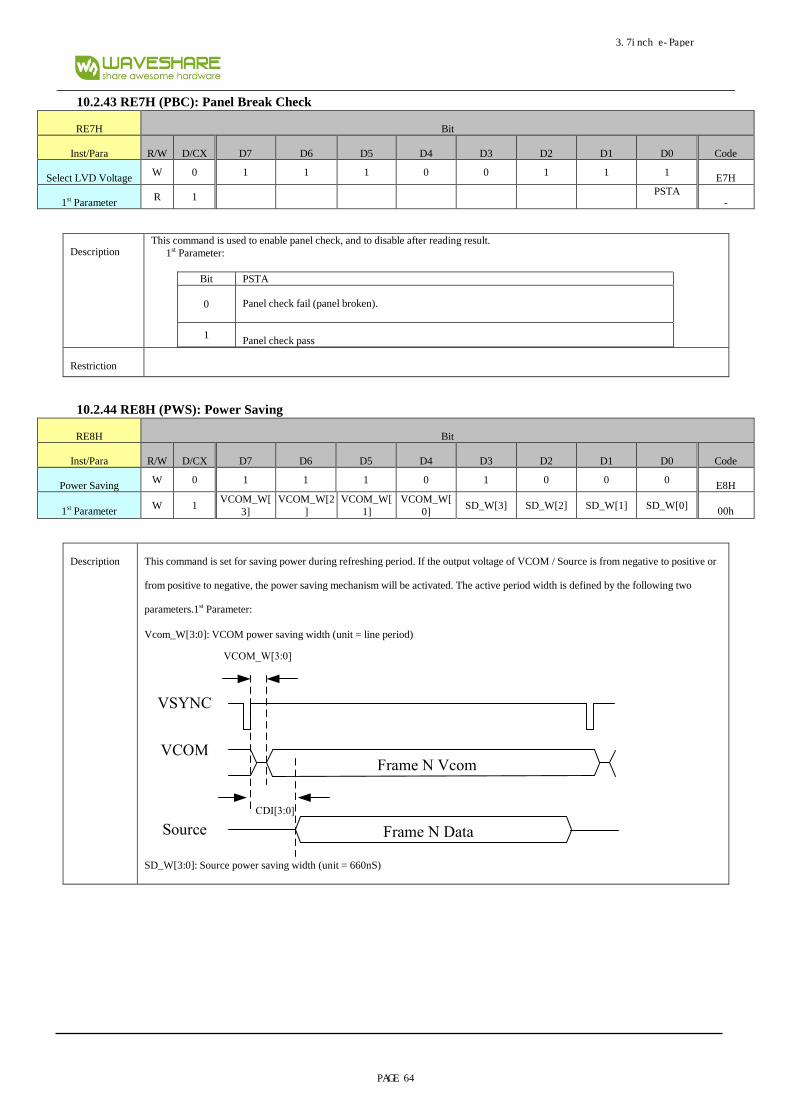
10.2.43 RE7H (PBC): Panel Break Check
RE7H Bit
Inst/Para R/W D/CX D7 D6 D5 D4 D3 D2 D1 D0 Code
Select LVD Voltage W 0 1 1 1 0 0 1 1 1 E7H
1st Parameter R 1 PSTA -
Description This command is used to enable panel check, and to disable after reading result.
1st Parameter:
Bit PSTA
0 Panel check fail (panel broken).
1 Panel check pass
Restriction
10.2.44 RE8H (PWS): Power Saving
RE8H Bit
Inst/Para R/W D/CX D7 D6 D5 D4 D3 D2 D1 D0 Code
Power Saving W 0 1 1 1 0 1 0 0 0 E8H
1st Parameter W 1 VCOM_W[
3] VCOM_W[2
] VCOM_W[
1] VCOM_W[
0] SD_W[3] SD_W[2] SD_W[1] SD_W[0] 00h
Description This command is set for saving power during refreshing period. If the output voltage of VCOM / Source is from negative to positive or
from positive to negative, the power saving mechanism will be activated. The active period width is defined by the following two
parameters.1st Parameter:
Vcom_W[3:0]: VCOM power saving width (unit = line period)
Frame N Vcom
Frame N Data
VSYNC
VCOM
Source
VCOM_W[3:0]
CDI[3:0]
SD_W[3:0]: Source power saving width (unit = 660nS)
3.7inch e-Paper
PAGE 64
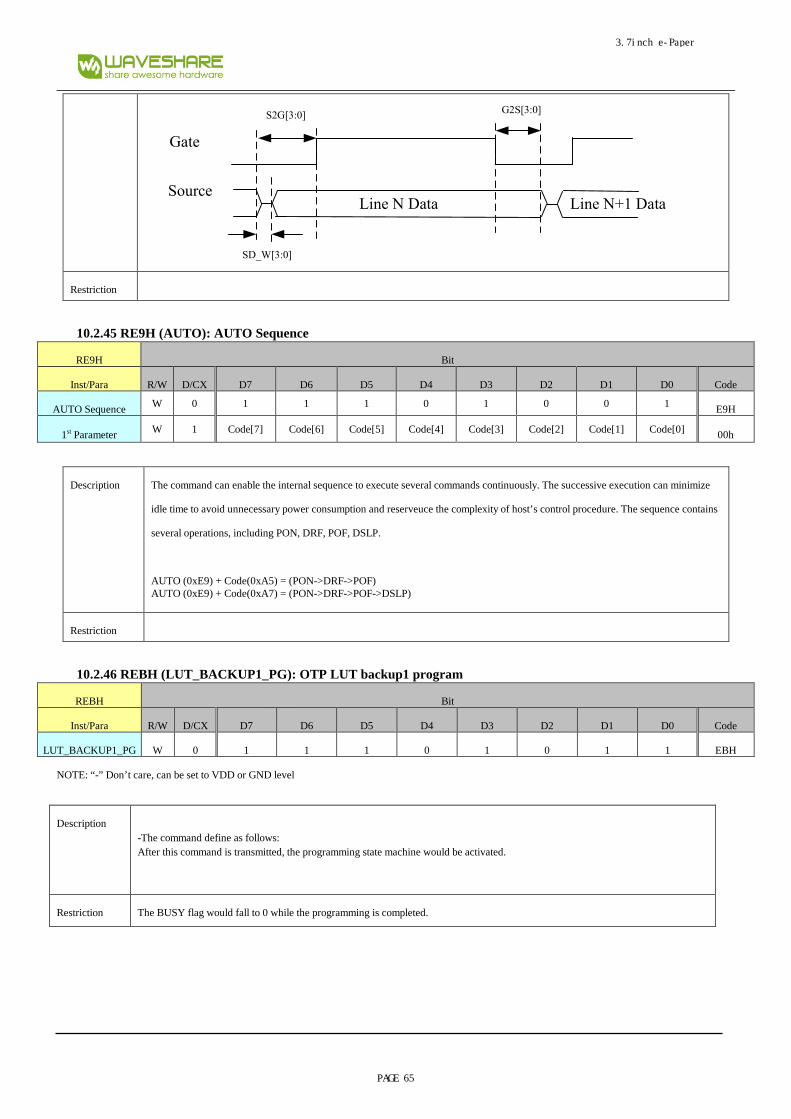
Line N DataSource
SD_W[3:0]
S2G[3:0]G2S[3:0]
Line N+1 Data
Gate
Restriction
10.2.45 RE9H (AUTO): AUTO Sequence
RE9H Bit
Inst/Para R/W D/CX D7 D6 D5 D4 D3 D2 D1 D0 Code
AUTO Sequence W 0 1 1 1 0 1 0 0 1 E9H
1st Parameter W 1 Code[7] Code[6] Code[5] Code[4] Code[3] Code[2] Code[1] Code[0] 00h
Description The command can enable the internal sequence to execute several commands continuously. The successive execution can minimize
idle time to avoid unnecessary power consumption and reserveuce the complexity of host’s control procedure. The sequence contains
several operations, including PON, DRF, POF, DSLP.
AUTO (0xE9) + Code(0xA5) = (PON->DRF->POF) AUTO (0xE9) + Code(0xA7) = (PON->DRF->POF->DSLP)
Restriction
10.2.46 REBH (LUT_BACKUP1_PG): OTP LUT backup1 program
REBH Bit
Inst/Para R/W D/CX D7 D6 D5 D4 D3 D2 D1 D0 Code
LUT_BACKUP1_PG W 0 1 1 1 0 1 0 1 1 EBH
NOTE: “-” Don’t care, can be set to VDD or GND level
Description -The command define as follows: After this command is transmitted, the programming state machine would be activated.
Restriction The BUSY flag would fall to 0 while the programming is completed.
3.7inch e-Paper
PAGE 65
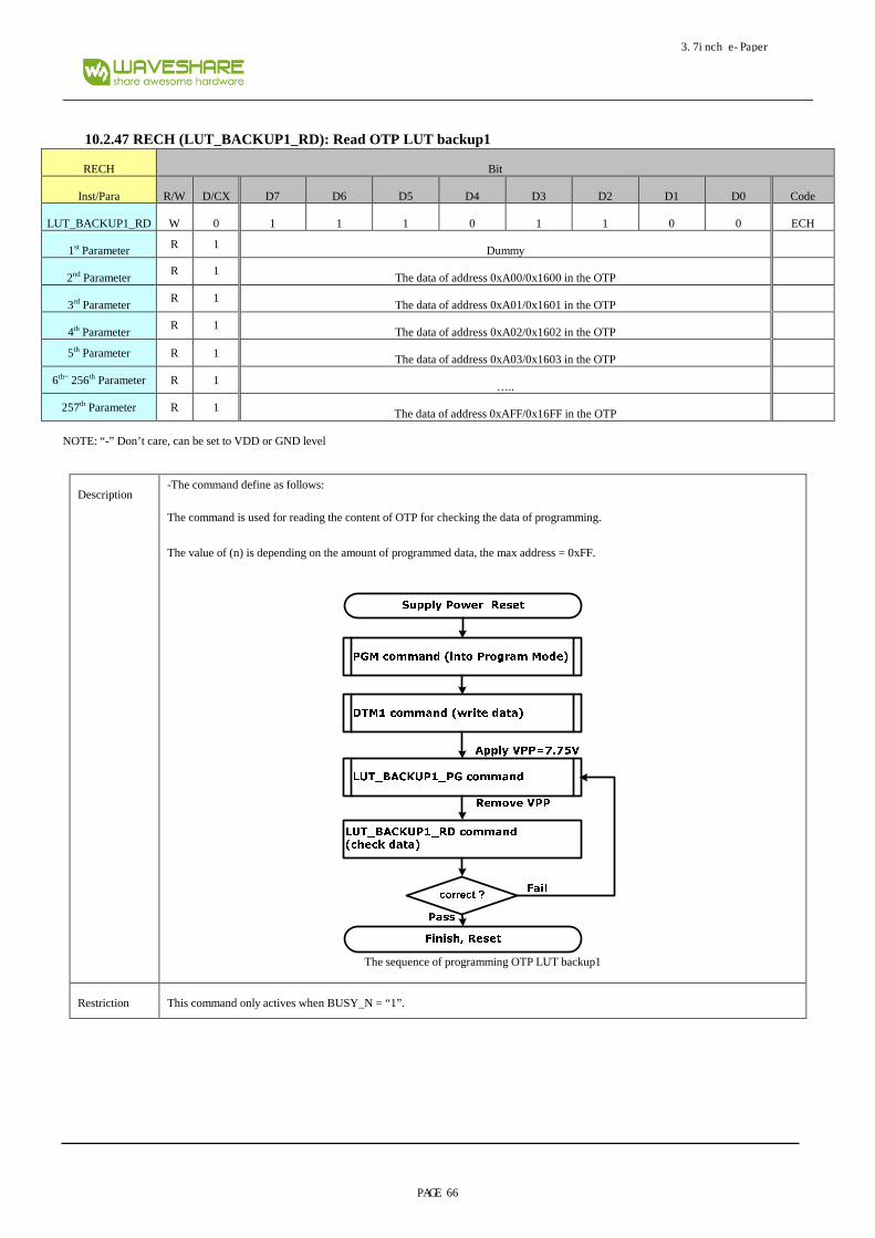
10.2.47 RECH (LUT_BACKUP1_RD): Read OTP LUT backup1
RECH Bit
Inst/Para R/W D/CX D7 D6 D5 D4 D3 D2 D1 D0 Code
LUT_BACKUP1_RD W 0 1 1 1 0 1 1 0 0 ECH
1st Parameter R 1 Dummy
2nd Parameter R 1
The data of address 0xA00/0x1600 in the OTP
3rd Parameter R 1
The data of address 0xA01/0x1601 in the OTP
4th Parameter R 1
The data of address 0xA02/0x1602 in the OTP
5th Parameter R 1 The data of address 0xA03/0x1603 in the OTP
6th~ 256th Parameter R 1 …..
257th Parameter R 1 The data of address 0xAFF/0x16FF in the OTP
NOTE: “-” Don’t care, can be set to VDD or GND level
Description -The command define as follows:
The command is used for reading the content of OTP for checking the data of programming.
The value of (n) is depending on the amount of programmed data, the max address = 0xFF.
The sequence of programming OTP LUT backup1
Restriction This command only actives when BUSY_N = “1”.
3.7inch e-Paper
PAGE 66
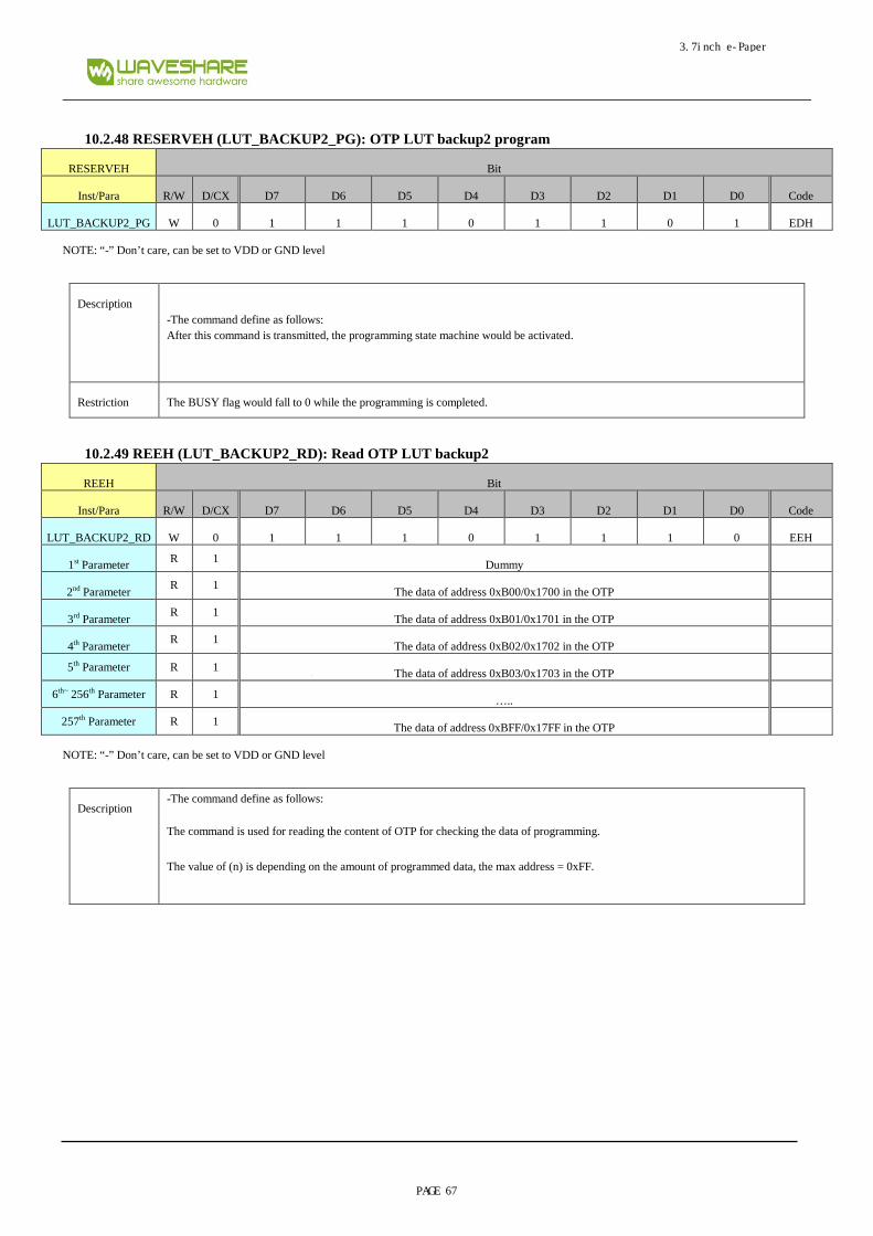
10.2.48 RESERVEH (LUT_BACKUP2_PG): OTP LUT backup2 program
RESERVEH Bit
Inst/Para R/W D/CX D7 D6 D5 D4 D3 D2 D1 D0 Code
LUT_BACKUP2_PG W 0 1 1 1 0 1 1 0 1 EDH
NOTE: “-” Don’t care, can be set to VDD or GND level
Description -The command define as follows: After this command is transmitted, the programming state machine would be activated.
Restriction The BUSY flag would fall to 0 while the programming is completed.
10.2.49 REEH (LUT_BACKUP2_RD): Read OTP LUT backup2
REEH Bit
Inst/Para R/W D/CX D7 D6 D5 D4 D3 D2 D1 D0 Code
LUT_BACKUP2_RD W 0 1 1 1 0 1 1 1 0 EEH
1st Parameter R 1 Dummy
2nd Parameter R 1
The data of address 0xB00/0x1700 in the OTP
3rd Parameter R 1
The data of address 0xB01/0x1701 in the OTP
4th Parameter R 1
The data of address 0xB02/0x1702 in the OTP
5th Parameter R 1 The data of address 0xB03/0x1703 in the OTP
6th~ 256th Parameter R 1 …..
257th Parameter R 1 The data of address 0xBFF/0x17FF in the OTP
NOTE: “-” Don’t care, can be set to VDD or GND level
Description -The command define as follows:
The command is used for reading the content of OTP for checking the data of programming.
The value of (n) is depending on the amount of programmed data, the max address = 0xFF.
3.7inch e-Paper
PAGE 67

The sequence of programming OTP LUT backup2
Restriction This command only actives when BUSY_N = “1”.
10.2.50 REFH (CHKSUM_PG): Checksum Program to OTP
REFH Bit
Inst/Para R/W D/CX D7 D6 D5 D4 D3 D2 D1 D0 Code
CHKSUM_PG W 0 1 1 1 0 1 0 1 1 EFH
Description
This command is used to Program Checksum of LUT Table
Restriction Apply VPP to OTP before use this command
3.7inch e-Paper
PAGE 68
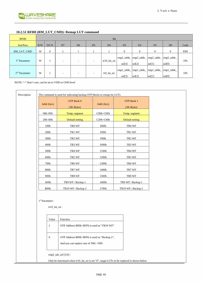
10.2.51 RF0H (RM_LUT_CMD): Remap LUT command
RF0H Bit
Inst/Para R/W D/CX D7 D6 D5 D4 D3 D2 D1 D0 Code
RM_LUT_CMD W 0 1 1 1 1 0 0 0 0 F0H
1st Parameter W 1 - - - tr10_lut_en rmp2_table_
sel[3]
rmp2_table_
sel[2]
rmp2_table_
sel[1]
rmp2_table_
sel[0] 1Fh
2nd Parameter W 1 - - - tr9_lut_en rmp1_table_
sel[3]
rmp1_table_
sel[2]
rmp1_table_
sel[1]
rmp1_table_
sel[0] 1Fh
NOTE: “-” Don’t care, can be set to VDD or GND level
Description The command is used for indicating backup OTP blocks to remap for LUTs
Addr (hex) OTP Bank 0
(3K Bytes) Addr (hex)
OTP Bank 1
(3K Bytes)
00h~0Fh Temp. segment C00h~C0Fh Temp. segment
20h~60h Default setting C20h~C60h Default setting
100h TR0 WF D00h TR0 WF
200h TR1 WF E00h TR1 WF
300h TR2 WF F00h TR2 WF
400h TR3 WF 1000h TR3 WF
500h TR4 WF 1100h TR4 WF
600h TR5 WF 1200h TR5 WF
700h TR6 WF 1300h TR6 WF
800h TR7 WF 1400h TR7 WF
900h TR8 WF 1500h TR8 WF
A00h TR9 WF / Backup 1 1600h TR9 WF / Backup 1
B00h TR10 WF / Backup 2 1700h TR10 WF / Backup 2
1st Parameter:
tr10_lut_en :
Value Function
1 OTP Address B00h~BFFh is used as “TR10 WF”
0 OTP Address B00h~BFFh is used as “Backup 2”,
And you can replace one of TR0 ~TR9.
rmp2_tab_sel [3:0] :
Only be functional when tr10_lut_en is set “0”, target LUTs to be replaced is shown below
3.7inch e-Paper
PAGE 69

Value Target LUTs
0001 TR0
0010 TR1
0011 TR2
0100 TR3
0101 TR4
0110 TR5
0111 TR6
1000 TR7
1001 TR8
1010 TR9
1011~1111 None
2nd Parameter
tr9_lut_en :
Value Function
1 OTP Address B00h~BFFh is used as “TR9 WF”
0 OTP Address B00h~BFFh is used as “Backup 1”,
And you can replace one of TR0 ~TR8.
rmp1_tab_sel[3:0]
Only be functional when tr9_lut_en is set “0”, target LUTs to be replaced is shown below
Value Target LUTs
0001 TR0
0010 TR1
0011 TR2
0100 TR3
0101 TR4
0110 TR5
0111 TR6
1000 TR7
1001 TR8
1010~1111 None
Notice : If rmp1_tab_sel = rmp2_tab_sel , the control hardware will reload “backup 1” block to replace target LUT.
3.7inch e-Paper
PAGE 70
Restriction
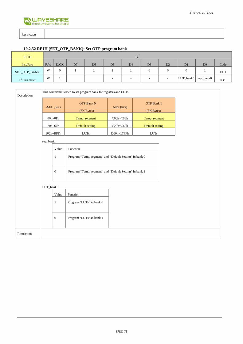
10.2.52 RF1H (SET_OTP_BANK): Set OTP program bank
RF1H Bit
Inst/Para R/W D/CX D7 D6 D5 D4 D3 D2 D1 D0 Code
SET_OTP_BANK W 0 1 1 1 1 0 0 0 1 F1H
1st Parameter W 1 - - - - LUT_bank0 reg_bank0 03h
Description This command is used to set program bank for registers and LUTs
Addr (hex) OTP Bank 0
(3K Bytes) Addr (hex)
OTP Bank 1
(3K Bytes)
00h~0Fh Temp. segment C00h~C0Fh Temp. segment
20h~60h Default setting C20h~C60h Default setting
100h~BFFh LUTs D00h~17FFh LUTs
reg_bank :
Value Function
1 Program “Temp. segment” and “Default Setting” in bank 0
0 Program “Temp. segment” and “Default Setting” in bank 1
LUT_bank :
Value Function
1 Program “LUTs” in bank 0
0 Program “LUTs” in bank 1
Restriction
3.7inch e-Paper
PAGE 71
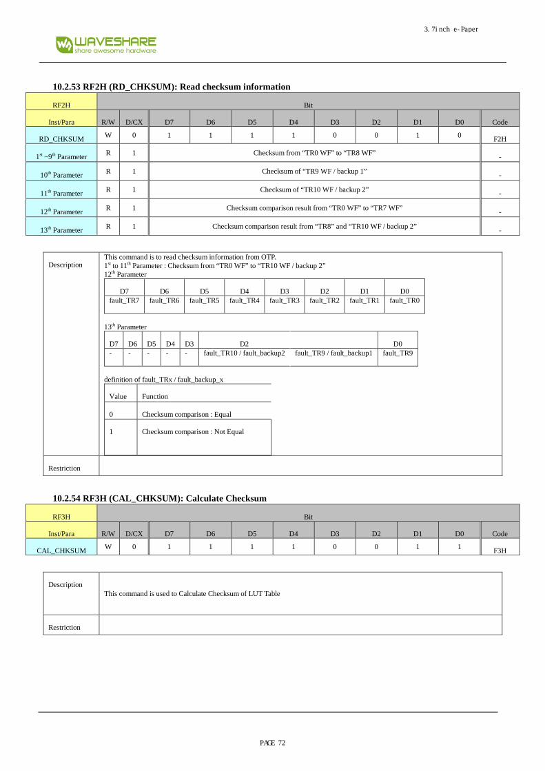
10.2.53 RF2H (RD_CHKSUM): Read checksum information
RF2H Bit
Inst/Para R/W D/CX D7 D6 D5 D4 D3 D2 D1 D0 Code
RD_CHKSUM W 0 1 1 1 1 0 0 1 0 F2H
1st ~9th Parameter R 1 Checksum from “TR0 WF” to “TR8 WF” -
10th Parameter R 1 Checksum of “TR9 WF / backup 1” -
11th Parameter R 1 Checksum of “TR10 WF / backup 2” -
12th Parameter R 1 Checksum comparison result from “TR0 WF” to “TR7 WF” -
13th Parameter R 1 Checksum comparison result from “TR8” and “TR10 WF / backup 2” -
Description This command is to read checksum information from OTP. 1st to 11th Parameter : Checksum from “TR0 WF” to “TR10 WF / backup 2” 12th Parameter
D7 D6 D5 D4 D3 D2 D1 D0 fault_TR7 fault_TR6 fault_TR5 fault_TR4 fault_TR3 fault_TR2 fault_TR1 fault_TR0
13th Parameter
D7 D6 D5 D4 D3 D2 D0 - - - - - fault_TR10 / fault_backup2 fault_TR9 / fault_backup1 fault_TR9
definition of fault_TRx / fault_backup_x
Value Function
0 Checksum comparison : Equal
1 Checksum comparison : Not Equal
Restriction
10.2.54 RF3H (CAL_CHKSUM): Calculate Checksum
RF3H Bit
Inst/Para R/W D/CX D7 D6 D5 D4 D3 D2 D1 D0 Code
CAL_CHKSUM W 0 1 1 1 1 0 0 1 1 F3H
Description This command is used to Calculate Checksum of LUT Table
Restriction
3.7inch e-Paper
PAGE 72

10-3) Register restriction
Register Refresh restriction BUSY_N flag R00H(PSR) X No action R01H(PWR) X No action R02H(POF) X Flag R03H(PFS) X No action R04H(PON) X Flag R05H(PMES) X No action R06H(BTST) X No action R07H(DSLP) X Flag R10H(DTM1) X No action R11H(DSP) Valid only read Flag R12H(DRF) X Flag R13H(DTM2) X No action R14H(PDTM1) X No action R15H(PDTM2) X No action R16H(PDRF) X Flag R20H(LUTC) X No action R21H(LUTWW) X No action R22H(LUTBW/LUTR) X No action R23H(LUTWB/LUTW) X No action R24H(LUTBB/LUTB) X No action R25H(LUTC Option) X No action R26H(SET_STG) Valid in BWR mode No action R30H(OSC) X No action R40H(TSC) Valid only read Flag R41H(TSE) X No action R42H(TSW) X No action R43H(TSR) Valid only read Flag R50H(CDI) X No action R51H(LPD) Valid only read No action R60H(TCON) X No action R61H(TRES) X No action R62H(TSGS) No action R70H(REV) Valid only read No action R71H(FLG) Valid only read No action R80H(AMV) Flag R81H(VV) Valid No action R82H(VDCS) X No action RA0H(PGM) X No action RA1H(APG) X Flag RA2H(ROTP) X Flag RE5H(TSSET) X No action RE6H(LVSEL) X No action RE7H (PBC) Valid (only read) No action RE8H (PWS) X No action RE9H (AUTO): Valid in standby Flag REBH X No action RECH X Flag REEH X No action REFH X Flag REFH (CHKSUM_PG) X No action RF0H (RM_LUT_CMD) X No action RF1H (SET_OTP_BANK) X No action RF2H (RD_CHKSUM) Valid only read No action RF3H (CAL_CHKSUM) X Flag
3.7inch e-Paper
PAGE 73
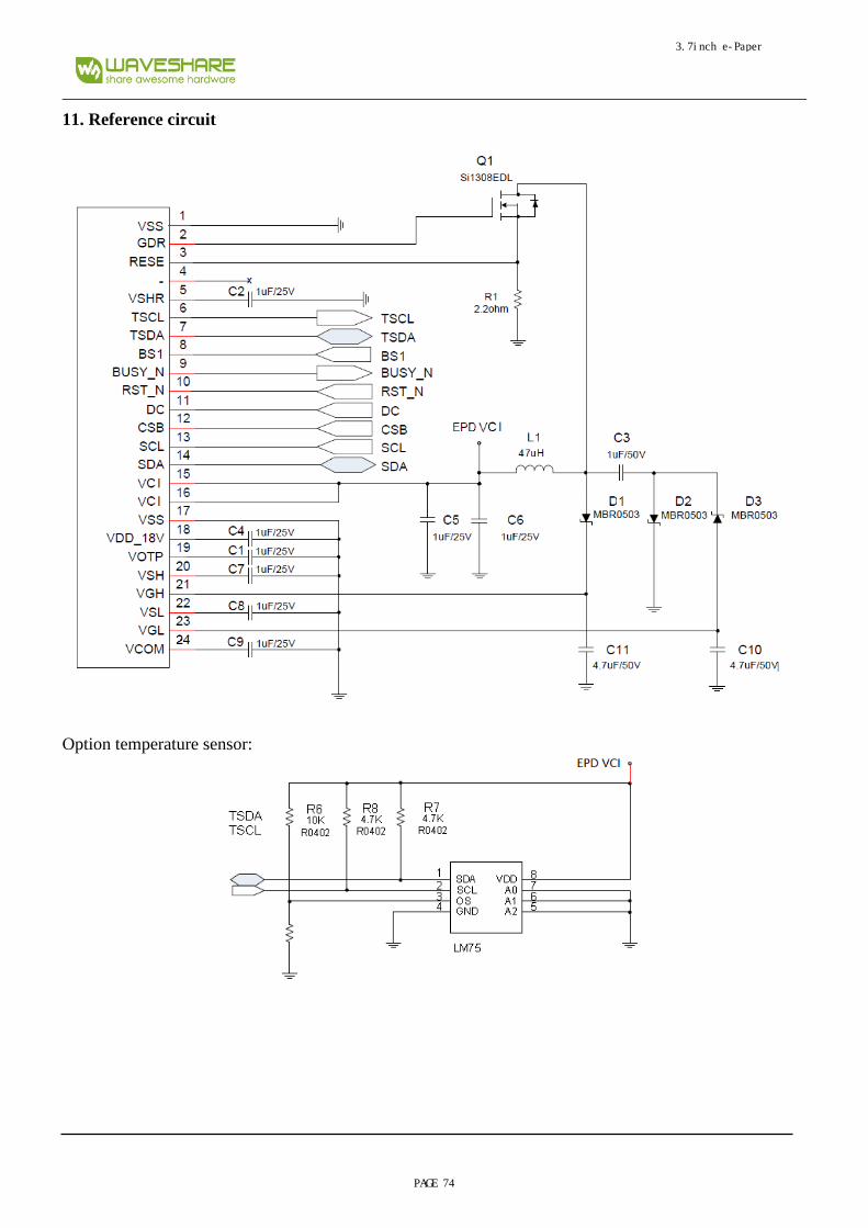
11. Reference circuit
Option temperature sensor:
3.7inch e-Paper
PAGE 74
12. Handling, safety and environment requirements
WARNING
The display TFT may break when it is dropped or bumped on a hard surface. Handle with care. Should the display
break, do not touch the electrophoretic material. In case of contact with electrophoretic material, wash with water
and soap.
CAUTION
The display module should not be exposed to harmful gases, such as acid and alkali gases, which corrode
electronic components.
Disassembling the display module can cause permanent damage and invalidate the warranty agreements.
Observe general precautions that are common to handling delicate electronic components. The TFT can break and
front surfaces can easily be damaged. Moreover the display is sensitive to static electricity and other rough
environmental conditions.
Data sheet status
Product specification This data sheet contains final product specifications.
Limiting values
Limiting values given are in accordance with the Absolute Maximum Rating System (IEC 134). Stress
above one or more of the limiting values may cause permanent damage to the device. These are stress
ratings only and operation of the device at these or at any other conditions above those given in the
characteristics sections of the specification is not implied. Exposure to limiting values for extended
periods may affect device reliability.
Application information
Where application information is given, it is advisory and does not form part of the specification.
3.7inch e-Paper
PAGE 75

13. Reliability testTEST CONDITION METHOD
1 High-Temperature Operation T = +40°C, RH = 30% for 240 hrs IEC 60 068-2-2Bp
2 Low-Temperature Operation T = 0°C for 240 hrs(150sec turn page) IEC 60 068-2-2Ab
3 High-Temperature Storage T = +60°C, RH=40% for 240 hrs
(Test In White Pattern) IEC 60 068-2-2Bp
4 Low-Temperature Storage T = -25°C for 240 hrs
(Test In White Pattern) IEC 60 068-2-1Ab
5 High-Temperature,
High-Humidity Operation T = +40°C, RH = 80% for 168 hrs IEC 60 068-2-3CA
6 High Temperature,
High- Humidity Storage T = +50℃, RH=80% for 240 hrs
(Test In White Pattern) IEC 60 068-2-3CA
7 Temperature Cycle -25℃ � +60℃, 50 Cycles
30mins 30 mins (Test In White Pattern)
IEC 60 068-2-14
8 Solar Radiation test 765 W/m2 for 168hrs,40℃
(Test In White Pattern) IEC60 068-2-5Sa
9 Package Vibration 1.04G, Frequency: 10~500Hz
Direction: X,Y,Z Duration: 1 hours in each direction
Full packed for shipment
10 Package Drop Impact
Drop from height of 122 cm on concrete surface.
Drop sequence: 1 corner, 3 edges, 6 faces One drop for each.
Full packed for shipment
11 Electrostatic Effect
(non-operating) (Air mode)+/-12kV; (Test in active area.)
(Contact mode)+/-8kV (Test in active area.) IEC 62179, IEC 62180
Actual EMC level to be measureserve on customer application
Note : The protective film must be removed before temperature test.
[Criteria] In the standard conditions, there is not display function NG issue occurreserve. (Including:line defect, no image) All the cosmetic specification is judged before the reliability stress.
3.7inch e-Paper
PAGE 76
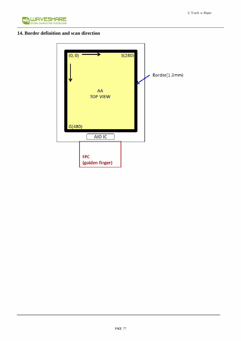
14. Border definition and scan direction
3.7inch e-Paper
PAGE 77

15. PackingTBD
3.7inch e-Paper
PAGE 78