Embed Size (px)
Citation preview
3.75 kV, 7-Channel, SPIsolator Multiple Slave, Digital Isolator for SPI
Data Sheet ADuM3154
Rev. B Document Feedback Information furnished by Analog Devices is believed to be accurate and reliable. However, no responsibility is assumed by Analog Devices for its use, nor for any infringements of patents or other rights of third parties that may result from its use. Specifications subject to change without notice. No license is granted by implication or otherwise under any patent or patent rights of Analog Devices. Trademarks and registered trademarks are the property of their respective owners.
One Technology Way, P.O. Box 9106, Norwood, MA 02062-9106, U.S.A. Tel: 781.329.4700 ©2014–2017 Analog Devices, Inc. All rights reserved. Technical Support www.analog.com
FEATURES Supports up to 17 MHz SPI clock speed 4 high speed, low propagation delay, SPI signal isolation
channels Supports up to 4 slave devices 20-lead SSOP package with 5.1 mm creepage High temperature operation: 125°C High common-mode transient immunity: >25 kV/µs Safety and regulatory approvals
UL recognition per UL 1577 3750 V rms for 1 minute
CSA Component Acceptance Notice 5A VDE certificate of conformity
DIN V VDE V 0884-10 (VDE V 0884-10):2006-12 VIORM = 565 V peak
APPLICATIONS Industrial programmable logic controllers (PLCs) Sensor isolation
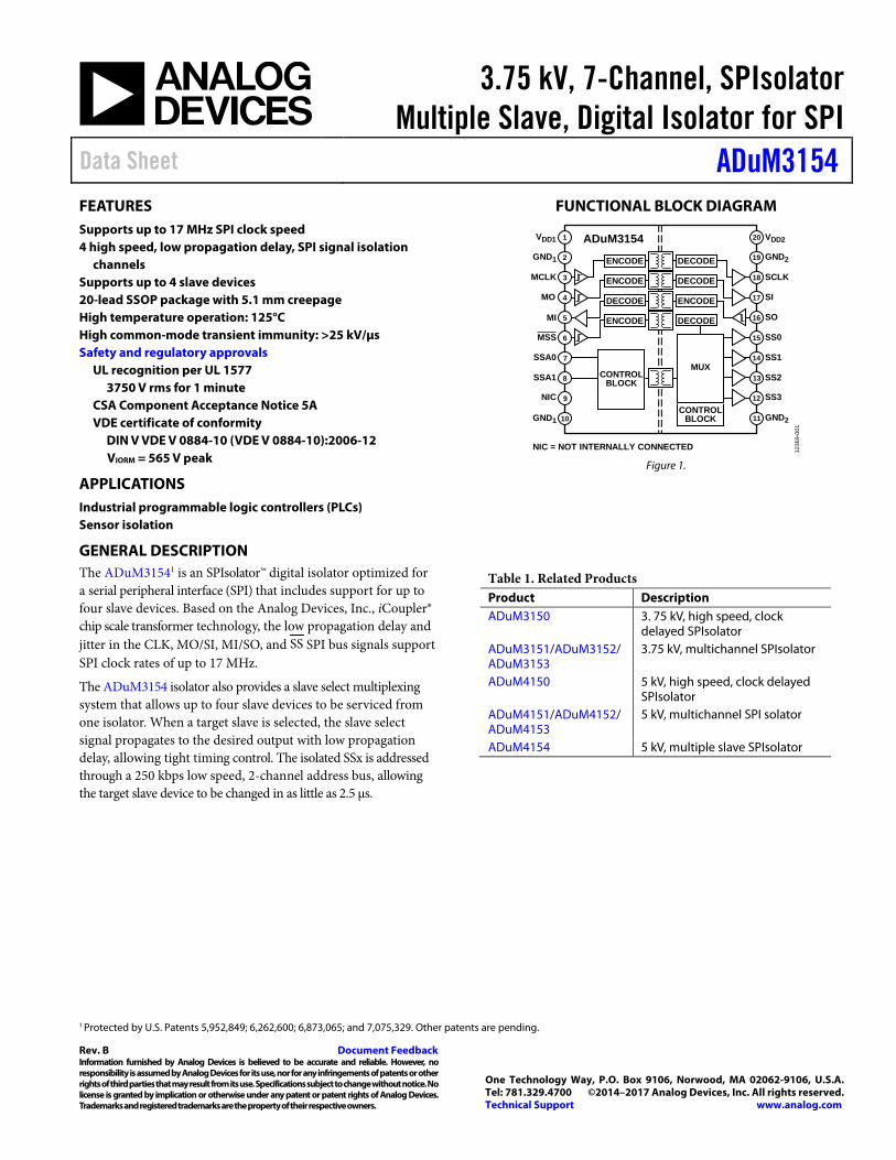
FUNCTIONAL BLOCK DIAGRAM
ENCODE
CONTROLBLOCK
DECODE
DECODE ENCODE
ENCODE DECODE
ENCODE DECODE
VDD1
GND1
MCLK
MO
MI
MSS
SSA0
SSA1
NIC
NIC = NOT INTERNALLY CONNECTED
VDD2
GND2
SCLK
SI
SO
SS0
SS1
SS2
SS3
1
2
3
4
5
6
7
8
20
19
18
17
16
15
14
13
GND1 GND2
9
10
12
11
ADuM3154
1236
9-00
1
CONTROLBLOCK
MUX
Figure 1.
GENERAL DESCRIPTION The ADuM31541 is an SPIsolator™ digital isolator optimized for a serial peripheral interface (SPI) that includes support for up to four slave devices. Based on the Analog Devices, Inc., iCoupler® chip scale transformer technology, the low propagation delay and jitter in the CLK, MO/SI, MI/SO, and SS SPI bus signals support SPI clock rates of up to 17 MHz.
The ADuM3154 isolator also provides a slave select multiplexing system that allows up to four slave devices to be serviced from one isolator. When a target slave is selected, the slave select signal propagates to the desired output with low propagation delay, allowing tight timing control. The isolated SSx is addressed through a 250 kbps low speed, 2-channel address bus, allowing the target slave device to be changed in as little as 2.5 µs.
Table 1. Related Products Product Description ADuM3150 3. 75 kV, high speed, clock
delayed SPIsolator ADuM3151/ADuM3152/ ADuM3153
3.75 kV, multichannel SPIsolator
ADuM4150 5 kV, high speed, clock delayed SPIsolator
ADuM4151/ADuM4152/ADuM4153
5 kV, multichannel SPI solator
ADuM4154 5 kV, multiple slave SPIsolator
1 Protected by U.S. Patents 5,952,849; 6,262,600; 6,873,065; and 7,075,329. Other patents are pending.

ADuM3154 Data Sheet
Rev. B | Page 2 of 22
TABLE OF CONTENTS Features .............................................................................................. 1 Applications ....................................................................................... 1 Functional Block Diagram .............................................................. 1 General Description ......................................................................... 1 Revision History ............................................................................... 2 Specifications ..................................................................................... 3
Electrical Characteristics—5 V Operation................................ 3 Electrical Characteristics—3.3 V Operation ............................ 5 Electrical Characteristics—Mixed 5 V/3.3 V Operation ........ 7 Electrical Characteristics—Mixed 3.3 V/5 V Operation ........ 9 Package Characteristics ............................................................. 10 Regulatory Information ............................................................. 11 Insulation and Safety Related Specifications .......................... 11 DIN V VDE V 0884-10 (VDE V 0884-10):2006-12 Insulation Characteristics ............................................................................ 12
Recommended Operating Conditions .................................... 12 Absolute Maximum Ratings ......................................................... 13
ESD Caution................................................................................ 13 Pin Configuration and Function Descriptions ........................... 14 Typical Performance Characteristics ........................................... 16 Applications Information .............................................................. 17
Introduction ................................................................................ 17 Printed Circuit Board (PCB) Layout ....................................... 19 Propagation Delay Related Parameters ................................... 19 DC Correctness and Magnetic Field Immunity ..................... 19 Power Consumption .................................................................. 20 Insulation Lifetime ..................................................................... 20
Outline Dimensions ....................................................................... 22 Ordering Guide .......................................................................... 22
REVISION HISTORY 7/2017—Rev. A to Rev. B Changes to Output Voltages Parameter, Table 5........................... 6 Changes to Output Voltages Parameter, Table 7........................... 8 Changes to Output Voltages Parameter, Table 9......................... 10 3/2015—Rev. 0 to Rev. A Changes to Features Section and Table 1 ...................................... 1 Changes to Supply Current Parameter, Table 3 ............................ 4 Changes to Supply Current Parameter, Table 5 ............................ 6 Changes to Supply Current Parameter, Table 7 ............................ 8 Changes to Supply Current Parameter, Table 9 and Table 10 ... 10 Changes to Table 11 ........................................................................ 11 Changes to Table 13 and Figure 2 ................................................. 12 Changes to High Speed Channels Section .................................. 17 Changes to Ordering Guide .......................................................... 22 7/2014—Revision 0: Initial Version
Data Sheet ADuM3154
Rev. B | Page 3 of 22
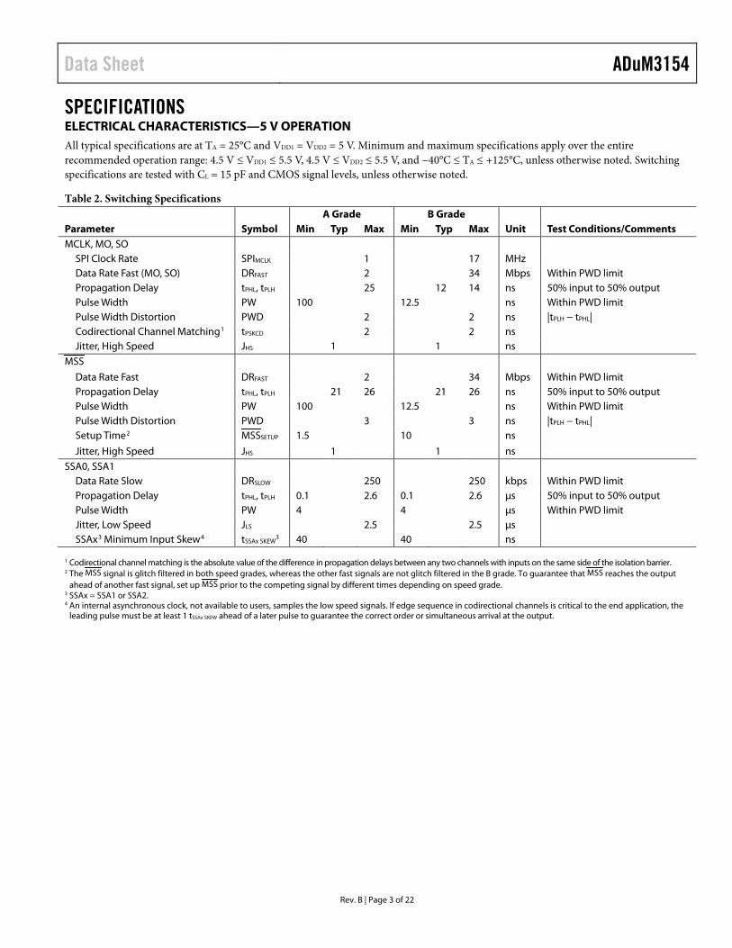
SPECIFICATIONS ELECTRICAL CHARACTERISTICS—5 V OPERATION All typical specifications are at TA = 25°C and VDD1 = VDD2 = 5 V. Minimum and maximum specifications apply over the entire recommended operation range: 4.5 V ≤ VDD1 ≤ 5.5 V, 4.5 V ≤ VDD2 ≤ 5.5 V, and −40°C ≤ TA ≤ +125°C, unless otherwise noted. Switching specifications are tested with CL = 15 pF and CMOS signal levels, unless otherwise noted.
Table 2. Switching Specifications
Parameter Symbol A Grade B Grade
Unit Test Conditions/Comments Min Typ Max Min Typ Max MCLK, MO, SO
SPI Clock Rate SPIMCLK 1 17 MHz Data Rate Fast (MO, SO) DRFAST 2 34 Mbps Within PWD limit Propagation Delay tPHL, tPLH 25 12 14 ns 50% input to 50% output Pulse Width PW 100 12.5 ns Within PWD limit Pulse Width Distortion PWD 2 2 ns |tPLH − tPHL| Codirectional Channel Matching1 tPSKCD 2 2 ns Jitter, High Speed JHS 1 1 ns
MSS
Data Rate Fast DRFAST 2 34 Mbps Within PWD limit Propagation Delay tPHL, tPLH 21 26 21 26 ns 50% input to 50% output Pulse Width PW 100 12.5 ns Within PWD limit Pulse Width Distortion PWD 3 3 ns |tPLH − tPHL| Setup Time2 MSSSETUP 1.5 10 ns
Jitter, High Speed JHS 1 1 ns SSA0, SSA1
Data Rate Slow DRSLOW 250 250 kbps Within PWD limit Propagation Delay tPHL, tPLH 0.1 2.6 0.1 2.6 µs 50% input to 50% output Pulse Width PW 4 4 µs Within PWD limit Jitter, Low Speed JLS 2.5 2.5 µs SSAx3 Minimum Input Skew4 tSSAx SKEW
3 40 40 ns 1 Codirectional channel matching is the absolute value of the difference in propagation delays between any two channels with inputs on the same side of the isolation barrier. 2 The MSS signal is glitch filtered in both speed grades, whereas the other fast signals are not glitch filtered in the B grade. To guarantee that MSS reaches the output
ahead of another fast signal, set up MSS prior to the competing signal by different times depending on speed grade. 3 SSAx = SSA1 or SSA2. 4 An internal asynchronous clock, not available to users, samples the low speed signals. If edge sequence in codirectional channels is critical to the end application, the
leading pulse must be at least 1 tSSAx SKEW ahead of a later pulse to guarantee the correct order or simultaneous arrival at the output.

ADuM3154 Data Sheet
Rev. B | Page 4 of 22
Table 3. For All Models1, 2, 3 Parameter Symbol Min Typ Max Unit Test Conditions/Comments SUPPLY CURRENT
A Grade and B Grade IDD1 4.8 8.5 mA CL = 0 pF, DRFAST = 1 MHz, DRSLOW = 0 MHz
IDD2 6.5 13 mA CL = 0 pF, DRFAST = 1 MHz, DRSLOW = 0 MHz
B Grade IDD1 10 18 mA CL = 0 pF, DRFAST = 17 MHz, DRSLOW = 0 MHz
IDD2 13.5 19 mA CL = 0 pF, DRFAST = 17 MHz, DRSLOW = 0 MHz
DC SPECIFICATIONS MCLK, MSS, MO, SO, SSA0, SSA1
Input Threshold Logic High VIH 0.7 × VDDx V Logic Low VIL 0.3 × VDDx V
Input Hysteresis VIHYST 500 mV Input Current per Channel II −1 +0.01 +1 µA 0 V ≤ VINPUT ≤ VDDx
SCLK, MI, SI, SS0, SS1, SS2, SS3 Output Voltages
Logic High VOH VDDx − 0.1 5.0 V IOUTPUT = −20 µA, VINPUT = VIH VDDx − 0.4 4.8 V IOUTPUT = −4 mA, VINPUT = VIH Logic Low VOL 0.0 0.1 V IOUTPUT = 20 µA, VINPUT = VIL 0.2 0.4 V IOUTPUT = 4 mA, VINPUT = VIL
VDD1, VDD2 Undervoltage Lockout UVLO 2.6 V Supply Current for High Speed Channels
Dynamic Input IDDI(D) 0.080 mA/Mbps Dynamic Output IDDO(D) 0.046 mA/Mbps
Supply Current for All Low Speed Channels Quiescent Input IDD1(Q) 4.2 mA Quiescent Output IDD2(Q) 6.1 mA
AC SPECIFICATIONS Output Rise/Fall Time tR/tF 2.5 ns 10% to 90% Common-Mode Transient Immunity4 |CM| 25 35 kV/µs VINPUT = VDDx, VCM = 1000 V,
transient magnitude = 800 V 1 VDDx = VDD1 or VDD2. 2 VINPUT is the input voltage of any of the MCLK, MSS, MO, SO, SSA0, or SSA1 pins. 3 IOUTPUT is the output current of any of the SCLK, MI, SI, SS0, SS1, SS2, or SS3 pins. 4 |CM| is the maximum common-mode voltage slew rate that can be sustained while maintaining output voltages within the VOH and VOL limits. The common-mode
voltage slew rates apply to both rising and falling common-mode voltage edges.

Data Sheet ADuM3154
Rev. B | Page 5 of 22
ELECTRICAL CHARACTERISTICS—3.3 V OPERATION All typical specifications are at TA = 25°C and VDD1 = VDD2 = 3.3 V. Minimum and maximum specifications apply over the entire recommended operation range: 3.0 V ≤ VDD1 ≤ 3.6 V, 3.0 V ≤ VDD2 ≤ 3.6 V, and −40°C ≤ TA ≤ +125°C, unless otherwise noted. Switching specifications are tested with CL = 15 pF and CMOS signal levels, unless otherwise noted.
Table 4. Switching Specifications
Parameter Symbol A Grade B Grade
Unit Test Conditions/Comments Min Typ Max Min Typ Max MCLK, MO, SO
SPI Clock Rate SPIMCLK 1 12.5 MHz Data Rate Fast (MO, SO) DRFAST 2 34 Mbps Within PWD limit Propagation Delay tPHL, tPLH 30 21 ns 50% input to 50% output Pulse Width PW 100 12.5 ns Within PWD limit Pulse Width Distortion PWD 3 2 ns |tPLH − tPHL| Codirectional Channel Matching1 tPSKCD 3 2 ns Jitter, High Speed JHS 1 1 ns
MSS
Data Rate Fast DRFAST 2 34 Mbps Within PWD limit Propagation Delay tPHL, tPLH 34 34 ns 50% input to 50% output Pulse Width PW 100 12.5 ns Within PWD limit Pulse Width Distortion PWD 3 3 ns |tPLH − tPHL| Setup Time2 MSSSETUP 1.5 10 ns
Jitter, High Speed JHS 1 1 ns SSA0, SSA1
Data Rate Slow DRSLOW 250 250 kbps Within PWD limit Propagation Delay tPHL, tPLH 0.1 2.6 0.1 2.6 µs 50% input to 50% output Pulse Width PW 4 4 µs Within PWD limit Jitter, Low Speed JLS 2.5 2.5 µs SSAx3 Minimum Input Skew4 tSSAx SKEW
3 40 40 ns 1 Codirectional channel matching is the absolute value of the difference in propagation delays between any two channels with inputs on the same side of the
isolation barrier. 2 The MSS signal is glitch filtered in both speed grades, whereas the other fast signals are not glitch filtered in the B grade. To guarantee that MSS reaches the
output ahead of another fast signal, set up MSS prior to the competing signal by different times depending on speed grade. 3 SSAx = SSA1 or SSA2. 4 An internal asynchronous clock, not available to users, samples the low speed signals. If edge sequence in codirectional channels is critical to the end
application, the leading pulse must be at least 1 tSSAx SKEW ahead of a later pulse to guarantee the correct order or simultaneous arrival at the output.

ADuM3154 Data Sheet
Rev. B | Page 6 of 22
Table 5. For All Models1, 2, 3 Parameter Symbol Min Typ Max Unit Test Conditions/Comments SUPPLY CURRENT
A Grade and B Grade IDD1 3.4 6.5 mA CL = 0 pF, DRFAST = 1 MHz, DRSLOW = 0 MHz
IDD2 5 9 mA CL = 0 pF, DRFAST = 1 MHz, DRSLOW = 0 MHz
B Grade IDD1 11.7 15 mA CL = 0 pF, DRFAST = 17 MHz, DRSLOW = 0 MHz
IDD2 10 14 mA CL = 0 pF, DRFAST = 17 MHz, DRSLOW = 0 MHz
DC SPECIFICATIONS MCLK, MSS, MO, SO, SSA0, SSA1
Input Threshold Logic High VIH 0.7 × VDDx V Logic Low VIL 0.3 × VDDx V
Input Hysteresis VIHYST 500 mV Input Current per Channel II −1 +0.01 +1 µA 0 V ≤ VINPUT ≤ VDDx
SCLK, MI, SI, SS0, SS1, SS2, SS3 Output Voltages
Logic High VOH VDDx − 0.1 3.3 V IOUTPUT = −20 µA, VINPUT = VIH VDDx − 0.4 3.1 V IOUTPUT = −4 mA, VINPUT = VIH Logic Low VOL 0.0 0.1 V IOUTPUT = 20 µA, VINPUT = VIL
0.2 0.4 V IOUTPUT = 4 mA, VINPUT = VIL VDD1, VDD2 Undervoltage Lockout UVLO 2.6 V Supply Current for High Speed Channels
Dynamic Input IDDI(D) 0.078 mA/Mbps Dynamic Output IDDO(D) 0.026 mA/Mbps
Supply Current for All Low Speed Channels Quiescent Input IDD1(Q) 2.9 mA Quiescent Output IDD2(Q) 4.7 mA
AC SPECIFICATIONS Output Rise/Fall Time tR/tF 2.5 ns 10% to 90% Common-Mode Transient Immunity4 |CM| 25 35 kV/µs VINPUT = VDDx, VCM = 1000 V,
transient magnitude = 800 V 1 VDDx = VDD1 or VDD2. 2 VINPUT is the input voltage of any of the MCLK, MSS, MO, SO, SSA0, or SSA1 pins. 3 IOUTPUT is the output current of any of the SCLK, MI, SI, SS0 SS1, SS2, or SS3 pins. 4 |CM| is the maximum common-mode voltage slew rate that can be sustained while maintaining output voltages within the VOH and VOL limits. The common-mode voltage slew rates apply to both rising and falling common-mode voltage edges.
Data Sheet ADuM3154
Rev. B | Page 7 of 22
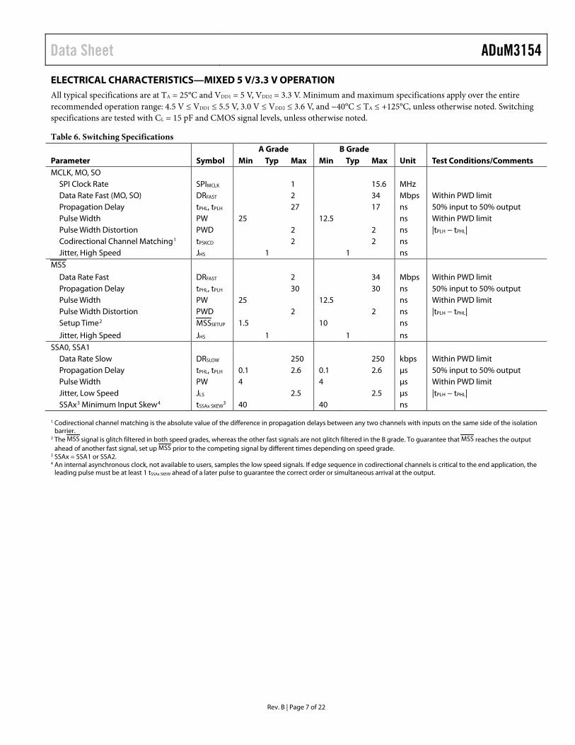
ELECTRICAL CHARACTERISTICS—MIXED 5 V/3.3 V OPERATION All typical specifications are at TA = 25°C and VDD1 = 5 V, VDD2 = 3.3 V. Minimum and maximum specifications apply over the entire recommended operation range: 4.5 V ≤ VDD1 ≤ 5.5 V, 3.0 V ≤ VDD2 ≤ 3.6 V, and −40°C ≤ TA ≤ +125°C, unless otherwise noted. Switching specifications are tested with CL = 15 pF and CMOS signal levels, unless otherwise noted.
Table 6. Switching Specifications
Parameter Symbol A Grade B Grade
Unit Test Conditions/Comments Min Typ Max Min Typ Max MCLK, MO, SO
SPI Clock Rate SPIMCLK 1 15.6 MHz Data Rate Fast (MO, SO) DRFAST 2 34 Mbps Within PWD limit Propagation Delay tPHL, tPLH 27 17 ns 50% input to 50% output Pulse Width PW 25 12.5 ns Within PWD limit Pulse Width Distortion PWD 2 2 ns |tPLH − tPHL| Codirectional Channel Matching1 tPSKCD 2 2 ns Jitter, High Speed JHS 1 1 ns
MSS
Data Rate Fast DRFAST 2 34 Mbps Within PWD limit Propagation Delay tPHL, tPLH 30 30 ns 50% input to 50% output Pulse Width PW 25 12.5 ns Within PWD limit Pulse Width Distortion PWD 2 2 ns |tPLH − tPHL| Setup Time2 MSSSETUP 1.5 10 ns
Jitter, High Speed JHS 1 1 ns SSA0, SSA1
Data Rate Slow DRSLOW 250 250 kbps Within PWD limit Propagation Delay tPHL, tPLH 0.1 2.6 0.1 2.6 µs 50% input to 50% output Pulse Width PW 4 4 µs Within PWD limit Jitter, Low Speed JLS 2.5 2.5 µs |tPLH − tPHL| SSAx3 Minimum Input Skew4 tSSAx SKEW
3 40 40 ns 1 Codirectional channel matching is the absolute value of the difference in propagation delays between any two channels with inputs on the same side of the isolation
barrier. 2 The MSS signal is glitch filtered in both speed grades, whereas the other fast signals are not glitch filtered in the B grade. To guarantee that MSS reaches the output
ahead of another fast signal, set up MSS prior to the competing signal by different times depending on speed grade. 3 SSAx = SSA1 or SSA2. 4 An internal asynchronous clock, not available to users, samples the low speed signals. If edge sequence in codirectional channels is critical to the end application, the
leading pulse must be at least 1 tSSAx SKEW ahead of a later pulse to guarantee the correct order or simultaneous arrival at the output.

ADuM3154 Data Sheet
Rev. B | Page 8 of 22
Table 7. For All Models1, 2, 3 Parameter Symbol Min Typ Max Unit Test Conditions/Comments SUPPLY CURRENT
A Grade and B Grade IDD1 4.8 8.5 mA CL = 0 pF, DRFAST = 1 MHz, DRSLOW = 0 MHz
IDD2 5 9 mA CL = 0 pF, DRFAST = 1 MHz, DRSLOW = 0 MHz
B Grade IDD1 10 18 mA CL = 0 pF, DRFAST = 17 MHz, DRSLOW = 0 MHz
IDD2 10 14 mA CL = 0 pF, DRFAST = 17 MHz, DRSLOW = 0 MHz
DC SPECIFICATIONS MCLK, MSS, MO, SO, SSA0, SSA1
Input Threshold Logic High VIH 0.7 × VDDx V Logic Low VIL 0.3 × VDDx V
Input Hysteresis VIHYST 500 mV Input Current per Channel II −1 +0.01 +1 µA 0 V ≤ VINPUT ≤ VDDX
SCLK, MI, SI, SS0, SS1, SS2, SS3 Output Voltages
Logic High VOH VDDx − 0.1 VDDx V IOUTPUT = −20 µA, VINPUT = VIH VDDx − 0.4 VDDx – 0.2 V IOUTPUT = −4 mA, VINPUT = VIH Logic Low VOL 0.0 0.1 V IOUTPUT = 20 µA, VINPUT = VIL
0.2 0.4 V IOUTPUT = 4 mA, VINPUT = VIL VDD1, VDD2 Undervoltage Lockout UVLO 2.6 V Supply Current for All Low Speed Channels
Quiescent Input IDD1(Q) 4.2 mA Quiescent Output IDD2(Q) 4.7 mA
AC SPECIFICATIONS Output Rise/Fall Time tR/tF 2.5 ns 10% to 90% Common-Mode Transient Immunity4 |CM| 25 35 kV/µs VINPUT = VDDx, VCM = 1000 V,
transient magnitude = 800 V 1 VDDx = VDD1 or VDD2. 2 VINPUT is the input voltage of any of the MCLK, MSS, MO, SO, SSA0, or SSA1 pins. 3 IOUTPUT is the output current of any of the SCLK, MI, SI, SS0, SS1, SS2, or SS3 pins. 4 |CM| is the maximum common-mode voltage slew rate that can be sustained while maintaining output voltages within the VOH and VOL limits. The common-mode
voltage slew rates apply to both rising and falling common-mode voltage edges.

Data Sheet ADuM3154
Rev. B | Page 9 of 22
ELECTRICAL CHARACTERISTICS—MIXED 3.3 V/5 V OPERATION All typical specifications are at TA = 25°C and VDD1 = 3.3 V, VDD2 = 5 V. Minimum and maximum specifications apply over the entire recommended operation range: 3.0 V ≤ VDD1 ≤ 3.6 V, 4.5 V ≤ VDD2 ≤ 5.5 V, and −40°C ≤ TA ≤ +125°C, unless otherwise noted. Switching specifications are tested with CL = 15 pF and CMOS signal levels, unless otherwise noted.
Table 8. Switching Specifications
Parameter Symbol A Grade B Grade
Unit Test Conditions/Comments Min Typ Max Min Typ Max MCLK, MO, SO
SPI Clock Rate SPIMCLK 1 15.6 MHz Data Rate Fast (MO, SO) DRFAST 2 34 Mbps Within PWD limit Propagation Delay tPHL, tPLH 28 17 ns 50% input to 50% output Pulse Width PW 100 12.5 ns Within PWD limit Pulse Width Distortion PWD 2 2 ns |tPLH − tPHL| Codirectional Channel Matching1 tPSKCD 2 2 ns
Jitter, High Speed JHS 1 1 ns MSS
Jitter 1 1 ns Data Rate Fast DRFAST 2 34 Mbps Within PWD limit Propagation Delay tPHL, tPLH 28 21 28 ns 50% input to 50% output Pulse Width PW 100 12.5 ns Within PWD limit Pulse Width Distortion PWD 2 2 ns |tPLH − tPHL| Setup Time2 MSSSETUP 1.5 10 ns
Jitter, High Speed JHS 1 1 ns SSA0, SSA1
Data Rate Slow DRSLOW 250 250 kbps Within PWD limit Propagation Delay tPHL, tPLH 0.1 2.6 0.1 2.6 µs 50% input to 50% output Pulse Width PW 4 4 µs Within PWD limit Jitter, Low Speed JLS 2.5 2.5 µs |tPLH − tPHL| SSAx3 Minimum Input Skew4 tSSAx SKEW
3 40 40 ns 1 Codirectional channel matching is the absolute value of the difference in propagation delays between any two channels with inputs on the same side of the isolation
barrier. 2 The MSS signal is glitch filtered in both speed grades, whereas the other fast signals are not glitch filtered in the B grade. To guarantee that MSS reaches the output
ahead of another fast signal, set up MSS prior to the competing signal by different times depending on speed grade. 3 SSAx = SSA1 or SSA2. 4 An internal asynchronous clock, not available to users, samples the low speed signals. If edge sequence in codirectional channels is critical to the end application, the
leading pulse must be at least 1 tSSAx SKEW ahead of a later pulse to guarantee the correct order or simultaneous arrival at the output.
ADuM3154 Data Sheet
Rev. B | Page 10 of 22
Table 9. For All Models1, 2, 3 Parameter Symbol Min Typ Max Unit Test Conditions/Comments SUPPLY CURRENT
A Grade and B Grade IDD 3.4 6.5 mA CL = 0 pF, DRFAST = 1 MHz, DRSLOW = 0 MHz
IDD2 6.5 13 mA CL = 0 pF, DRFAST = 1 MHz, DRSLOW = 0 MHz
B Grade IDD 11.7 15 mA CL = 0 pF, DRFAST = 17 MHz, DRSLOW = 0 MHz
IDD2 13.5 19 mA CL = 0 pF, DRFAST = 17 MHz, DRSLOW = 0 MHz
DC SPECIFICATIONS MCLK, MSS, MO, SO, SSA0, SSA1
Input Threshold Logic High VIH 0.7 × VDDx V Logic Low VIL 0.3 × VDDx V
Input Hysteresis VIHYST 500 mV Input Current per Channel II −1 +0.01 +1 µA 0 V ≤ VINPUT ≤ VDDx
SCLK, MI, SI, SS0, SS1, SS2, SS3 Output Voltages
Logic High VOH VDDx − 0.1 VDDx V IOUTPUT = −20 µA, VINPUT = VIH VDDx − 0.4 VDDx – 0.2 V IOUTPUT = −4 mA, VINPUT = VIH Logic Low VOL 0.0 0.1 V IOUTPUT = 20 µA, VINPUT = VIL
0.2 0.4 V IOUTPUT = 4 mA, VINPUT = VIL VDD1, VDD2 Undervoltage Lockout UVLO 2.6 V Supply Current for All Low Speed Channels
Quiescent Input IDD1Q) 2.9 mA Quiescent Output IDD2(Q) 6.1 mA
AC SPECIFICATIONS Output Rise/Fall Time tR/tF 2.5 ns 10% to 90% Common-Mode Transient Immunity4 |CM| 25 35 kV/µs VINPUT = VDDx, VCM = 1000 V,
transient magnitude = 800 V 1 VDDx = VDD1 or VDD2. 2 VINPUT is the input voltage of any of the MCLK, MSS, MO, SO, SSA0, or SSA1 pins. 3 IOUTPUT is the output current of any of the SCLK, MI, SI, SS0, SS1, SS2, or SS3 pins. 4 |CM| is the maximum common-mode voltage slew rate that can be sustained whereas maintaining output voltages within the VOH and VOL limits. The common-mode voltage slew rates apply to both rising and falling common-mode voltage edges.
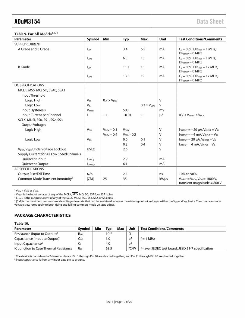
PACKAGE CHARACTERISTICS
Table 10. Parameter Symbol Min Typ Max Unit Test Conditions/Comments Resistance (Input to Output)1 RI-O 1012 Ω Capacitance (Input to Output)1 CI-O 1.0 pF f = 1 MHz Input Capacitance2 CI 4.0 pF IC Junction to Case Thermal Resistance θJC 68.5 °C/W 4-layer JEDEC test board, JESD 51-7 specification 1 The device is considered a 2-terminal device: Pin 1 through Pin 10 are shorted together, and Pin 11 through Pin 20 are shorted together. 2 Input capacitance is from any input data pin to ground.

Data Sheet ADuM3154
Rev. B | Page 11 of 22
REGULATORY INFORMATION The ADuM3154 is approved by the organizations listed in Table 11. See Table 16 and the Insulation Lifetime section for recommended maximum working voltages for specific cross isolation waveforms and insulation levels.
Table 11. UL CSA VDE Recognized under 1577 Component
Recognition Program1 Approved under CSA Component Acceptance Notice #5A
Certified according to DIN V VDE V 0884-10 (VDE V 0884-10):2006-122
3750 V rms Single Protection Basic insulation per CSA 60950-1-07+A1+A2 and IEC 60950-1 2nd Ed.+A1+A2, 510 V rms (721 V peak) maximum working voltage3
Reinforced insulation, 565 V peak
File E214100 File 205078 File 2471900-4880-0001 1 In accordance with UL 1577, each ADuM3154 is proof tested by applying an insulation test voltage ≥4500 V rms for 1 second (current leakage detection limit = 10 µA). 2 In accordance with DIN V VDE V 0884-10, each ADuM3154 is proof tested by applying an insulation test voltage ≥525 V peak for 1 second (partial discharge detection
limit = 5 pC). The asterisk (*) marked on the component designates DIN V VDE V 0884-10 approval. 3 See Table 16 for recommended maximum working voltages under various operating conditions.
INSULATION AND SAFETY RELATED SPECIFICATIONS
Table 12. Parameter Symbol Value Unit Test Conditions/Comments Rated Dielectric Insulation Voltage 3750 V rms 1 minute duration Minimum External Air Gap (Clearance) L(I01) 5.1 mm min Measured from input terminals to output terminals,
shortest distance through air Minimum External Tracking (Creepage) L(I02) 5.1 mm min Measured from input terminals to output terminals,
shortest distance path along body Minimum Internal Gap (Internal Clearance) 0.017 mm min Distance through insulation Tracking Resistance (Comparative Tracking Index) CTI >400 V DIN IEC 112/VDE 0303 Part 1 Material Group II Material group (DIN VDE 0110, 1/89, Table 1)

ADuM3154 Data Sheet
Rev. B | Page 12 of 22
DIN V VDE V 0884-10 (VDE V 0884-10):2006-12 INSULATION CHARACTERISTICS This isolator is suitable for reinforced electrical isolation only within the safety limit data. Maintenance of the safety data is ensured by protective circuits. The asterisk (*) marked on packages denotes DIN V VDE V 0884-10 approval.
Table 13. Description Test Conditions/Comments Symbol Characteristic Unit Installation Classification per DIN VDE 0110
For Rated Mains Voltage ≤ 150 V rms I to IV For Rated Mains Voltage ≤ 300 V rms I to III For Rated Mains Voltage ≤ 400 V rms I to II Climatic Classification 40/105/21
Pollution Degree per DIN VDE 0110, Table 1 2 Maximum Working Insulation Voltage VIORM 565 V peak Input-to-Output Test Voltage, Method b1 VIORM × 1.875 = Vpd(m), 100% production test,
tini = tm = 1 sec, partial discharge < 5 pC Vpd(m) 1059 V peak
Input-to-Output Test Voltage, Method a After Environmental Tests Subgroup 1 VIORM × 1.5 = Vpd(m), tini = 60 sec, tm = 10 sec,
partial discharge < 5 pC Vpd(m) 848 V peak
After Input and/or Safety Test Subgroup 2 and Subgroup 3
VIORM × 1.2 = Vpd(m), tini = 60 sec, tm = 10 sec, partial discharge < 5 pC
Vpd(m) 678 V peak
Highest Allowable Overvoltage VIOTM 5000 V peak Surge Isolation Voltage VIOSM(TEST) = 10 kV, 1.2 µs rise time, 50 µs,
50% fall time VIOSM 6250 V peak
Safety Limiting Values Maximum value allowed in the event of a failure (see Figure 2)
Case Temperature TS 150 °C Safety Total Dissipated Power IS1 1.4 W
Insulation Resistance at TS VIO = 500 V RS >109 Ω
1.6
1.8
2.0
1.4
1.2
1.0
0.8
0.6
0.4
0.2
00 50 200100 150
1236
9-00
2
SAFE
LIM
ITIN
G P
OW
ER (W
)
AMBIENT TEMPERATURE (°C) Figure 2. Thermal Derating Curve, Dependence of Safety Limiting Values
with Case Temperature per DIN V VDE V 0884-10
RECOMMENDED OPERATING CONDITIONS
Table 14. Parameter Symbol Min Max Unit Operating Temperature Range TA −40 +125 °C Supply Voltage Range1 VDD1,
VDD2 3.0 5.5 V
Input Signal Rise and Fall Times 1.0 ms 1 See the DC Correctness and Magnetic Field Immunity section for information
on the immunity to the external magnetic fields.

Data Sheet ADuM3154
Rev. B | Page 13 of 22
ABSOLUTE MAXIMUM RATINGS TA = 25°C, unless otherwise noted
Table 15. Parameter Rating Storage Temperature (TST) Range −65°C to +150°C Ambient Operating Temperature
(TA) Range −40°C to +125°C
Supply Voltages (VDD1, VDD2) −0.5 V to +7.0 V Input Voltages (MCLK, MSS, MO, SO,
SSA0, SSA1) −0.5 V to VDDx + 0.5 V
Output Voltages (SCLK, MI, SI, SS0 SS1, SS2, SS3)
−0.5 V to VDDx + 0.5 V
Average Output Current per Pin1 −10 mA to +10 mA Common-Mode Transients2 −100 kV/µs to +100 kV/µs
1 See Figure 2 for maximum safety rated current values across temperature. 2 Refers to common-mode transients across the insulation barrier. Common-
mode transients exceeding the absolute maximum ratings may cause latch-up or permanent damage.
Stresses at or above those listed under Absolute Maximum Ratings may cause permanent damage to the product. This is a stress rating only; functional operation of the product at these or any other conditions above those indicated in the operational section of this specification is not implied. Operation beyond the maximum operating conditions for extended periods may affect product reliability.
Table 16. Maximum Continuous Working Voltage1 Parameter Max Unit Constraint AC 60 Hz
RMS Voltage 400 V rms 20-year lifetime at 0.1%
failure rate, zero average voltage
DC Voltage 722 V peak Limited by the creepage of the package, Pollution Degree 2, Material Group II2, 3
1 See the Insulation Lifetime section for details. 2 Other pollution degree and material group requirements yield a different limit. 3 Some system level standards allow components to use the printed wiring
board (PWB) creepage values. The supported dc voltage may be higher for those standards.
ESD CAUTION
ADuM3154 Data Sheet
Rev. B | Page 14 of 22
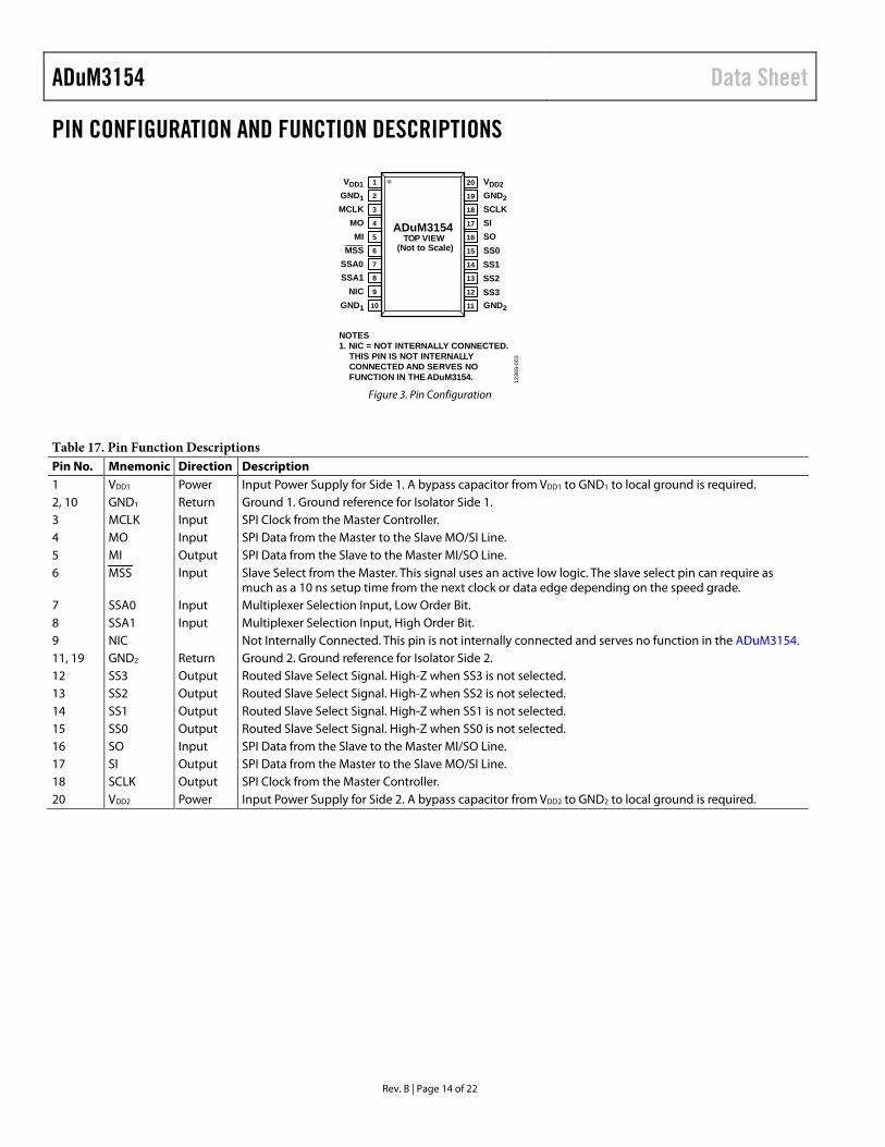
PIN CONFIGURATION AND FUNCTION DESCRIPTIONS
VDD1 1
GND1 2
MCLK 3
MO 4
20
19
18
17
MI 5
MSS 6
SSA0 7
16
15
14
SSA1 8 13
NIC
NOTES1. NIC = NOT INTERNALLY CONNECTED. THIS PIN IS NOT INTERNALLY CONNECTED AND SERVES NO FUNCTION IN THE ADuM3154.
9 12
GND1
VDD2GND2SCLKSISOSS0SS1SS2SS3GND210 11
1236
9-00
3
ADuM3154(Not to Scale)
TOP VIEW
Figure 3. Pin Configuration
Table 17. Pin Function Descriptions Pin No. Mnemonic Direction Description 1 VDD1 Power Input Power Supply for Side 1. A bypass capacitor from VDD1 to GND1 to local ground is required. 2, 10 GND1 Return Ground 1. Ground reference for Isolator Side 1. 3 MCLK Input SPI Clock from the Master Controller. 4 MO Input SPI Data from the Master to the Slave MO/SI Line. 5 MI Output SPI Data from the Slave to the Master MI/SO Line. 6 MSS Input Slave Select from the Master. This signal uses an active low logic. The slave select pin can require as
much as a 10 ns setup time from the next clock or data edge depending on the speed grade. 7 SSA0 Input Multiplexer Selection Input, Low Order Bit. 8 SSA1 Input Multiplexer Selection Input, High Order Bit. 9 NIC Not Internally Connected. This pin is not internally connected and serves no function in the ADuM3154. 11, 19 GND2 Return Ground 2. Ground reference for Isolator Side 2. 12 SS3 Output Routed Slave Select Signal. High-Z when SS3 is not selected. 13 SS2 Output Routed Slave Select Signal. High-Z when SS2 is not selected. 14 SS1 Output Routed Slave Select Signal. High-Z when SS1 is not selected. 15 SS0 Output Routed Slave Select Signal. High-Z when SS0 is not selected. 16 SO Input SPI Data from the Slave to the Master MI/SO Line. 17 SI Output SPI Data from the Master to the Slave MO/SI Line. 18 SCLK Output SPI Clock from the Master Controller. 20 VDD2 Power Input Power Supply for Side 2. A bypass capacitor from VDD2 to GND2 to local ground is required.
Data Sheet ADuM3154
Rev. B | Page 15 of 22
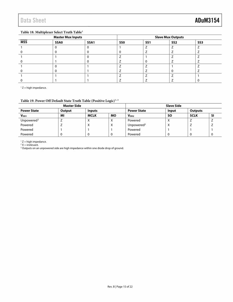
Table 18. Multiplexer Select Truth Table1 Master Mux Inputs Slave Mux Outputs
MSS SSA0 SSA1 SS0 SS1 SS2 SS3 1 0 0 1 Z Z Z 0 0 0 0 Z Z Z 1 1 0 Z 1 Z Z 0 1 0 Z 0 Z Z 1 0 1 Z Z 1 Z 0 0 1 Z Z 0 Z 1 1 1 Z Z Z 1 0 1 1 Z Z Z 0 1 Z = high impedance.
Table 19. Power Off Default State Truth Table (Positive Logic)1, 2
Master Side Slave Side Power State Output Inputs Power State Input Outputs VDD1 MI MCLK MO VDD2 SO SCLK SI Unpowered3 Z X X Powered X Z Z Powered Z X X Unpowered3 X Z Z Powered 1 1 1 Powered 1 1 1 Powered 0 0 0 Powered 0 0 0 1 Z = high impedance. 2 X = irrelevant. 3 Outputs on an unpowered side are high impedance within one diode drop of ground.

ADuM3154 Data Sheet
Rev. B | Page 16 of 22
TYPICAL PERFORMANCE CHARACTERISTICS
0
1
2
3
4
5
7
6
0 20 40 60 80DATA RATE (Mbps)
3.3V5.0V
1236
9-00
4
DYN
AM
IC S
UPP
LY C
UR
REN
TPE
R IN
PUT
CH
AN
NE
L (m
A)
Figure 4. Typical Dynamic Supply Current per Input Channel vs. Data Rate for 5.0 V and 3.3 V Operation
0
5
10
15
20
25
30
0 20 40 60 80
I DD
1 SU
PPLY
CU
RR
ENT
(mA
)
DATA RATE (Mbps)
3.3V
5.0V
1236
9-00
6
Figure 5. Typical IDD1 Supply Current vs. Data Rate for 5.0 V and 3.3 V Operation
0
2
4
6
8
10
12
14
16
–40 10 60 110
PRO
PAG
ATIO
N D
ELAY
(ns)
AMBIENT TEMPERATURE (°C)
3.3V
5.0V
1236
9-00
8
Figure 6. Typical Propagation Delay vs. Ambient Temperature for High Speed
Channels Without Glitch Filter (See the High Speed Channels Section)
1236
9-00
50
0.5
1.0
1.5
2.0
2.5
3.0
3.5
4.0
0 20 40 60 80DATA RATE (Mbps)
3.3V
5.0V
DYN
AM
IC S
UPP
LY C
UR
REN
TPE
R O
UTP
UT
CH
AN
NE
L (m
A)
Figure 7. Typical Dynamic Supply Current per Output Channel vs. Data Rate for 5.0 V and 3.3 V Operation
0
5
10
15
20
25
0 20 40 60 80
I DD
2 SU
PPLY
CU
RR
ENT
(mA
)
DATA RATE (Mbps)
3.3V
5.0V
1236
9-00
7
Figure 8. Typical IDD2 Supply Current vs. Data Rate for 5.0 V and 3.3 V Operation
–40 10 60 110AMBIENT TEMPERATURE (°C)
3.3V
5.0V
0
5
10
15
20
25
PRO
PAG
ATIO
N D
ELAY
(ns)
1236
9-00
9
Figure 9. Typical Propagation Delay vs. Ambient Temperature for High Speed
Channels with Glitch Filter (See the High Speed Channels Section)

Data Sheet ADuM3154
Rev. B | Page 17 of 22
APPLICATIONS INFORMATION INTRODUCTION The ADuM3154 was created to optimize isolation of the SPI for speed and provide additional low speed channels for control and status monitoring functions. The isolator is based on differential signaling iCoupler technology for enhanced speed and noise immunity.
High Speed Channels
The ADuM3154 has four high speed channels. The first three channels, CLK, MI/SO, and MO/SI (the slash indicates the connection of the particular input and output channel across the isolator), are optimized for either low propagation delay in the B grade, or high noise immunity in the A grade. The difference between the grades is the addition of a glitch filter to these three channels in the A grade version, which increases the propagation delay. The B grade version, with a maximum propagation delay of 14 ns, supports a maximum clock rate of 17 MHz in standard 4-wire SPI. However, because the glitch filter is not present in the B grade version, ensure that spurious glitches of less than 10 ns are not present.
Glitches of less than 10 ns in the B grade devices can cause the second edge of the glitch to be missed. This pulse condition is then seen as a spurious data transition on the output that is corrected by a refresh or the next valid data edge. It is recommended to use the A grade devices in noisy environments.
The relationship between the SPI signal paths and the pin mnemonics of the ADuM3154 and data directions is detailed in Table 20.
Table 20. Pin Mnemonics Correspondence to SPI Signal Path Names SPI Signal Path
Master Side 1
Data Direction
Slave Side 2
CLK MCLK → SCLK MO/SI MO → SI MI/SO MI ← SO SS MSS → SSx
The datapaths are SPI mode agnostic. The CLK and MOSI SPI datapaths are optimized for propagation delay and channel to channel matching. The MISO SPI datapath is optimized for propagation delay. The device does not synchronize to the clock channel; therefore, there are no constraints on the clock polarity or the timing with respect to the data line. To allow compatibility with nonstandard SPI interfaces, the MI pin is always active, and does not tristate when the slave select is not asserted. This precludes tying several MI lines together without adding a trisate buffer or multiplexor.
The SS (slave select bar) is typically an active low signal. It can have many different functions in SPI and SPI like busses. Many of these functions are edge triggered, so the SS path contains a glitch filter in both the A grade and the B grade. The glitch filter prevents short pulses from propagating to the output or causing other errors in operation. The MSS signal requires a 10 ns setup time in the B grade devices prior to the first active clock edge to allow the added propagation time of the glitch filter.
Slave Select Multiplexer
The ADuM3154 can control up to four independent slave devices. Figure 10 shows how this can be done using general-purpose isolators. An isolation channel is required for each slave select; therefore, seven high speed channels are required to transfer bidirectional data to four slaves.
MASTERISOLATOR
SLAVE 0CLK
MOSI
MISO
1236
9-01
0
SS0
CLK
MOSI
MISO
SS0
SLAVE 1CLK
MOSI
MISO
SS1
SLAVE 2CLK
MOSI
MISO
SS2
SLAVE 3CLK
MOSI
MISO
SS3
SS1
SS2
SS3
Figure 10. Multiple Slave Control with Standard Isolators

ADuM3154 Data Sheet
Rev. B | Page 18 of 22
Figure 11 shows how the ADuM3154 can control up to four slaves by routing the MSS input to one of four outputs on the slave side of the isolator, which eliminates three isolation channels compared to the standard solution.
MASTER ADuM3154
SLAVE 0CLK
MOSI
MISO
1236
9-01
1
MUX
CLK
MOSI
MISO
SS0
SLAVE 1CLK
MOSI
MISO
SS1
SLAVE 2CLK
MOSI
MISO
SS2
SLAVE 3CLK
MOSI
MISO
SS3
SSA0
SSA1
MSS
Figure 11. Multiple Slave Control
The multiplexer select lines are low speed channels implemented as part of the dc correctness scheme in the ADuM3154. The dc value of all high and low speed inputs on a given side of the device are sampled simultaneously, packetized, and shifted across an isolation coil. The high speed channels are compared for dc accuracy, and the low speed mux select lines, SSA0 and SSA1, are transferred to the mux control block. The dc correctness data for the high speed channels is handled internally with no visibility off chip.
This data is regulated by a free running internal clock. Because data is sampled at discrete times based on this clock, the propagation delay for mux select lines is between 100 ns and 2.6 µs depending on where the input data edge changes with respect to the internal sample clock. After an address propagation delay time of up to 2.6 µs, the multiplexer routes the MSS signals to the desired output. The outputs that are not selected are set to high-Z, and the application pulls them to the desired idle state.
Figure 12 illustrates the behavior of the SSA0 and SSA1 channels. This diagram assumes that MSS is low and that SS0, SS1, SS2, and SS3 are pulled up.
SSA0
SS0
SAMPLE CLOCK
OUTPUT CLOCK
B
CSSA1
SS1SS2
SS3
A
B
C
1236
9-01
2
A
A
Figure 12. Mux Select Timing
The following details the mux select timing shown in Figure 12:
• Point A: The mux select lines must be switched simultaneously to within the tSSAx SKEW time. Failure to do this may allow sampling the inputs between the edges and selecting an incorrect mux output. Point A on SS1 is a metastable state on the output mux resulting from wide spacing between SSA0 and SSA1.
• Point B: For mux select lines to be processed predictably, a state of SSA0 and SSA1 must be stable for longer than 4 µs before switching the mux to another output. This guarantees that at least two samples are taken of the inputs before the mux output is changed.
• Point C: This point in Figure 12 shows a clean transfer between SS3 being active and SS0 being active. The mux was designed to eliminate any short duration metastable states between any two selected outputs.

Data Sheet ADuM3154
Rev. B | Page 19 of 22
PRINTED CIRCUIT BOARD (PCB) LAYOUT The ADuM3154 digital isolator requires no external interface circuitry for the logic interfaces. Power supply bypassing is strongly recommended at both input and output supply pins, VDD1 and VDD2 (see Figure 13). The capacitor value must be between 0.01 µF and 0.1 µF. The total lead length between both ends of the capacitor and the input power supply pin must not exceed 20 mm.
BYPASS < 2mm
1236
9-01
3
VDD1
GND1
MCLKMO
MIMSS
SSA0
SSA1
VDD2GND2SCLK
SISO
SS0SS1SS2
NICGND1
SS3GND2
ADuM3154TOP VIEW
(Not to Scale)
Figure 13. Recommended PCB Layout
In applications involving high common-mode transients, it is important to minimize board coupling across the isolation barrier. Furthermore, design the board layout so that any coupling that does occur affects all pins equally on a given component side. Failure to ensure this can cause voltage differentials between pins exceeding the absolute maximum ratings of the device, thereby leading to latch-up or permanent damage.
PROPAGATION DELAY RELATED PARAMETERS Propagation delay is a parameter that describes the time it takes a logic signal to propagate through a component. The input to output propagation delay time for a high to low transition may differ from the propagation delay time of a low to high transition.
INPUT
OUTPUT
tPLH tPHL
50%
50%
1236
9-01
4
Figure 14. Propagation Delay Parameters
Pulse width distortion is the maximum difference between these two propagation delay values and an indication of how accurately the timing of the input signal is preserved.
Channel to channel matching refers to the maximum amount the propagation delay differs between channels within a single ADuM3154 component.
DC CORRECTNESS AND MAGNETIC FIELD IMMUNITY Positive and negative logic transitions at the isolator input cause narrow (~1 ns) pulses to be sent via the transformer to the decoder. The decoder is bistable and is, therefore, either set or reset by the pulses indicating input logic transitions. In the absence of logic transitions at the input for more than ~1.2 µs, a periodic set of refresh pulses indicative of the correct input state are sent via the low speed channel to ensure dc correctness at the output.
If the low speed decoder receives no pulses for more than about 5 µs, the input side is assumed to be unpowered or nonfunctional, in which case, the isolator output is forced to a high-Z state by the watchdog timer circuit.
The limitation on the magnetic field immunity of the device is set by the condition in which induced voltage in the transformer receiving coil is sufficiently large to either falsely set or reset the decoder. The following analysis defines such conditions. The ADuM3154 is examined in a 3 V operating condition because it represents the most susceptible mode of operation for this product.
The pulses at the transformer output have an amplitude greater than 1.5 V. The decoder has a sensing threshold of about 1.0 V; thereby establishing a 0.5 V margin in which induced voltages can be tolerated. The voltage induced across the receiving coil is given by
V = (−dβ/dt)Σπrn2; n = 1, 2, …, N
where: β is the magnetic flux density. rn is the radius of the nth turn in the receiving coil. N is the number of turns in the receiving coil.
Given the geometry of the receiving coil in the ADuM3154 and an imposed requirement that the induced voltage be, at most, 50% of the 0.5 V margin at the decoder, a maximum allowable magnetic field is calculated, as shown in Figure 15.
MAGNETIC FIELD FREQUENCY (Hz)
MA
XIM
UM
ALL
OW
AB
LE M
AG
NET
IC F
LUX
DEN
SITY
(kga
uss)
1k0.001
100
100M
10
1
0.1
0.01
10k 100k 1M 10M
1236
9-01
5
Figure 15. Maximum Allowable External Magnetic Flux Density

ADuM3154 Data Sheet
Rev. B | Page 20 of 22
For example, at a magnetic field frequency of 1 MHz, the maximum allowable magnetic field of 0.5 kgauss induces a voltage of 0.25 V at the receiving coil. This is about 50% of the sensing threshold and does not cause a faulty output transition. If such an event occurs, with the worst-case polarity, during a transmitted pulse, it reduces the received pulse from >1.0 V to 0.75 V, which is still well above the 0.5 V sensing threshold of the decoder.
The preceding magnetic flux density values correspond to specific current magnitudes at given distances away from the ADuM3154 transformers. Figure 16 expresses these allowable current magnitudes as a function of frequency for selected distances. The ADuM3154 is insensitive to external fields. Only extremely large, high frequency currents very close to the component are potentially a concern. For the 1 MHz example noted, a user would have to place a 1.2 kA current 5 mm away from the ADuM3154 to affect component operation.
MAGNETIC FIELD FREQUENCY (Hz)
MA
XIM
UM
ALL
OW
AB
LE C
UR
REN
T (k
A)
1000
100
10
1
0.1
0.011k 10k 100M100k 1M 10M
DISTANCE = 5mm
DISTANCE = 1m
DISTANCE = 100mm
1236
9-01
6
Figure 16. Maximum Allowable Current for
Various Current to ADuM3154 Spacings
At combinations of a strong magnetic field and high frequency, any loops formed by the PCB traces may induce sufficiently large error voltages to trigger the thresholds of succeeding circuitry. Take care to avoid PCB structures that form loops.
POWER CONSUMPTION The supply current at a given channel of the ADuM3154 isolator is a function of the supply voltage, the data rate of the channel, the output load of the channel, and whether it is a high or low speed channel.
The low speed channels draw a constant quiescent current caused by the internal ping-pong datapath. The operating frequency is low enough that the capacitive losses caused by the recommended capacitive load are negligible compared to the quiescent current. The explicit calculation for the data rate is eliminated for simplicity, and the quiescent current for each side of the isolator due to the low speed channels can be found in Table 3, Table 5, Table 7, and Table 9 for the particular operating voltages.
These quiescent currents add to the high speed current as is shown in the following equations for the total current for each side of the isolator. Dynamic currents are taken from Table 3 and Table 5 for the respective voltages.
For Side 1, the supply current is given by
( )( )( )( ) DD1(Q)DD1L(MI)DDO(D)MI
MOMCLKDDI(D)DD1
IVCIf
fffII
+×××+×
+++×=−3
MSS
105.0
For Side 2, the supply current is given by
( )( )( )( )( )( )( )( )( ) (Q)DDDDL(SSx)DDO(D)SSx
DDL(SI)DDO(D)SI
DDL(SCLK)DDO(D)SCLK
SODDI(D)DD
IVCIf
VCIf
VCIf
fII
223
23
23
2
105.0
105.0
105.0
+×××+×
+×××+×
+×××+×
+×=
−
−
−
where: IDDI(D), IDDO(D) are the input and output dynamic supply currents per channel (mA/Mbps). fX is the logic signal data rate for the specified channel (Mbps). CL(x) is the load capacitance of the specified output (pF). VDDx is the supply voltage of the side being evaluated (V). IDD1(Q), IDD2(Q) are the specified Side 1 and Side 2 quiescent supply currents (mA).
Figure 4 and Figure 7 show the supply current per channel as a function of data rate for an input and unloaded output. Figure 5 and Figure 8 show the total IDD1 and IDD2 supply currents as a function of data rate for ADuM3154 channel configurations with all high speed channels running at the same speed and the low speed channels at idle.
INSULATION LIFETIME All insulation structures eventually break down when subjected to voltage stress over a sufficiently long period. The rate of insulation degradation is dependent on the characteristics of the voltage waveform applied across the insulation, as well as the materials and material interfaces.
Two types of insulation degradation are of primary interest: breakdown along surfaces exposed to the air and insulation wear out. Surface breakdown is the phenomenon of surface tracking and the primary determinant of surface creepage requirements in system level standards. Insulation wear out is the phenomenon where charge injection or displacement currents inside the insulation material cause long-term insulation degradation.
Surface Tracking
Surface tracking is addressed in electrical safety standards by setting a minimum surface creepage based on the working voltage, the environmental conditions, and the properties of the insulation material. Safety agencies perform characterization testing on the surface insulation of components that allow the components to be categorized in different material groups. Lower material group ratings are more resistant to surface tracking and, therefore, can provide adequate lifetime with

Data Sheet ADuM3154
Rev. B | Page 21 of 22
smaller creepage. The minimum creepage for a given working voltage and material group is in each system level standard and is based on the total rms voltage across the isolation, pollution degree, and material group. The material group and creepage for the ADuM3154 isolator are detailed in Table 12.
Insulation Wear Out
The lifetime of insulation caused by wear out is determined by its thickness, the material properties, and the voltage stress applied. It is important to verify that the product lifetime is adequate at the application working voltage. The working voltage supported by an isolator for wear out may not be the same as the working voltage supported for tracking. It is the working voltage applicable to tracking that is specified in most standards.
Testing and modeling have shown that the primary driver of long-term degradation is displacement current in the polyimide insulation causing incremental damage. The stress on the insulation can be broken down into two broad categories, such as dc stress, which causes very little wear out because there is no displacement current, and an ac component time varying voltage stress, which causes wear out.
The ratings in certification documents are usually based on 60 Hz sinusoidal stress, because this reflects isolation from line voltage. However, many practical applications have combinations of 60 Hz ac and dc across the barrier, as shown in Equation 1. Because only the ac portion of the stress causes wear out, the equation can be rearranged to solve for the ac rms voltage, as shown in Equation 2. For insulation wear out with the polyimide materials used in this product, the ac rms voltage determines the product lifetime.
22DCRMSACRMS VVV += (1)
or
22DCRMSRMSAC VVV −= (2)
where: VRMS is the total rms working voltage. VAC RMS is the time varying portion of the working voltage. VDC is the dc offset of the working voltage.
Calculation and Use of Parameters Example
The following is an example that frequently arises in power conversion applications. Assume that the line voltage on one side of the isolation is 240 VAC RMS, and a 400 VDC bus voltage is present on the other side of the isolation barrier. The isolator
material is polyimide. To establish the critical voltages in determining the creepage clearance and lifetime of a device, see Figure 17 and the following equations.
ISO
LATI
ON
VO
LTA
GE
TIME
VAC RMS
VRMS VDC
1236
9-01
7
VPEAK
Figure 17. Critical Voltage Example
The working voltage across the barrier from Equation 1 is
22DCRMSACRMS VVV +=
22 400240 +=RMSV
VRMS = 466 V
This is the working voltage used together with the material group and pollution degree when looking up the creepage required by a system standard.
To determine if the lifetime is adequate, obtain the time varying portion of the working voltage. The ac rms voltage can be obtained from Equation 2.
22DCRMSRMSAC VVV −=
22 400466 −=RMSACV
VAC RMS = 240 VRMS
In this case, the VAC RMS is simply the line voltage of 240 VRMS. This calculation is more relevant when the waveform is not sinusoidal. The value is compared to the limits for the working voltage listed in Table 16 or the expected lifetime, under a 60 Hz sine wave, and it is well within the limit for a 50-year service life.
Note that the dc working voltage limit in Table 16 is set by the creepage of the package as specified in IEC 60664-1. This value may differ for specific system level standards.

ADuM3154 Data Sheet
Rev. B | Page 22 of 22
OUTLINE DIMENSIONS
COMPLIANT TO JEDEC STANDARDS MO-150-AE 0601
06-A
20 11
101
7.507.206.90
8.207.807.40
5.605.305.00
SEATINGPLANE
0.05 MIN
0.65 BSC
2.00 MAX
0.380.22COPLANARITY
0.10
1.851.751.65
0.250.09
0.950.750.55
8°4°0°
Figure 18. 20-Lead Shrink Small Outline Package [SSOP]
(RS-20) Dimensions shown in millimeters
ORDERING GUIDE
Model1
No. of Inputs, VDD1 Side
No. of Inputs, VDD2 Side
Maximum Data Rate (MHz)
Maximum Propagation Delay, 5 V (ns)
Isolation Rating (V rms)
Temperature Range
Package Description
Package Option
ADuM3154ARSZ 5 1 1 25 3750 −40°C to +125°C 20-Lead SSOP RS-20 ADuM3154ARSZ-RL7 5 1 1 25 3750 −40°C to +125°C 20-Lead SSOP,
7” Tape and Reel
RS-20
ADuM3154BRSZ 5 1 17 14 3750 −40°C to +125°C 20-Lead SSOP RS-20 ADuM3154BRSZ-RL7 5 1 17 14 3750 −40°C to +125°C 20-Lead SSOP,
7” Tape and Reel
RS-20
EVAL-ADuM3154Z Evaluation Board
1 Z = RoHS Compliant Part.
©2014–2017 Analog Devices, Inc. All rights reserved. Trademarks and registered trademarks are the property of their respective owners. D12369-0-7/17(B)