Embed Size (px)
Citation preview

02049-DSH-002-J Mindspeed Technologies® March 2010Mindspeed Proprietary and Confidential
M02049-15 3.3/5V Limiting Amplifier for Applications to 6.144 Gbps
Applications• 2.5 Gbps STM-16/OC-48 SDH/SONET• 1.06, 2.12 and 4.24 Gbps Fibre Channel• 1.25 Gbps Ethernet• 1.25 Gbps SDH/SONET• 2.67 Gbps SDH/SONET with FEC• Supports all CPRI data rates: 614.4, 1228.8, 2457.6, 3072.0, 4915.2
and 6144.0 Mbit/s
The M02049-15 is an integrated high-gain limiting amplifier. Featuring CML outputs, the M02049-15 is usable in applications to 6.144 Gbps. Full output swing is achieved even at minimum input sensitivity. The M02049-15 can operate with a 3.3V or 5V supply.
Rate select is supported for SFP applications and/or to achieve optimum sensitivity at data rates ≤ 1.25 Gbps. When rate select is high, optimum sensitivity is achieved at 2.5 Gbps and operation up to 6.144 Gbps is possible with reduced sensitivity.
The M02049-15 also includes two analog RSSI outputs proportional to either the average or peak to peak input signal and a programmable signal-level detector allowing the user to set thresholds at which the logic outputs are enabled. The M02043-15 is pin compatible with the M02049-15 and offers the same performance but does not include the rate select function.
Other available solutions: M02050-15 3.3/5V Limiting Amplifier for Applications to 2.5 Gbps (PECL outputs)M02040-15 3.3/5V Limiting Amplifier for Applications to 2.125 Gbps (PECL outputs)M02043-15 3.3/5V Limiting Amplifier for Applications to 6.144 Gbps (CML outputs)
1.25 Gbps and 4.25 Gbps SFP reference designs available on Mindspeed.com
Typical Applications Diagram
optional
LevelDetect
LimitingAmplifier
ComparatorLevelShift
CMLP
CMLN
RSSIPP
RATE SEL
AMPSET
Offset cancel
OutputBuffer
ThresholdSettingCircuit Regulator
VCCSTSET VCC3
Biasing
IREFJam
LOS
RAMPSET
RST
12.1 k Ω
VTT
T I A
Photodiode
+3.3 V
DINN
RxAVGIN
RSSIAVG
DINP
AC-Coupledto TIA
REXT
MON
M02013
AC or DC Coupled(as described in
Applications Information)
Clock DataRecovery
Unit
RATESELControl
Features• Operates with a 3.3V or 5V supply• 2.6 mV typical input sensitivity at 2.5 Gbps• CML outputs• Rate Selection for ≤ 1.25 Gbps operation• Average Receive power monitor output (RSSIAVG)• Peak-to-peak Receive power monitor output (RSSIPP)• On-chip DC offset cancellation circuit• Low power (< 90 mW)• Programmable CML Output Amplitude Level• Output Jam Function• 16 pin 3x3 QFN package
02049-DSH-002-J Mindspeed Technologies®2
Mindspeed Proprietary and Confidential
M02049-15 Typical Eye Diagram M02049-15 Pin Configuration
Ordering InformationPart Number Package Operating Temperature
M02049-15 16 pin, 3mm x 3mm QFN –40 °C to 85 °C
M02049G-15* 16 pin, 3mm x 3mm QFN, RoHS compliant –40 °C to 85 °C
M02049-15EVM Evaluation board with M02049-15 device –40 °C to 85 °C
* The letter “G” designator after the part number indicates that the device is RoHS-compliant. Refer to www.mindspeed.com for additional information.
Revision History
Revision Level Date ASIC Revision Description
J Release March 2010 -15 Added CPRI data rates to front page, specifications and typical eye diagrams.
H Release October 2006 -15 Added M02049G-15 part number in ordering information. Modified Input AC coupling capacitor information in section 4.1.3.
G Release July 2006 -15 Corrected an error in the DC specifications. Minimum CML High swing Output Amplitude now correctly reads 300 mV.
F Release August 2005 -15 Correct Jam connection in block diagram and typical applications figures. Correct IREF figure (reference current generation).
10 mVPP differential input2.5 Gbps
50 mV/div70 ps/div
AMPSET
CMLN
VCC
RATE
SEL
I REF
JAM
LOS
RSSI
PP
DINN
GND
DINPCMLP
1
4
5
9
12
1316
8
STSE
T
V CC3
RxAvgIN
RSSI
AVG
Center Pad
Connect to GND

02049-DSH-002-J
1.0 Product Specification
1.1 Absolute Maximum RatingsThese are the absolute maximum ratings at or beyond which the IC can be expected to fail or be damaged. Reliable operation at these extremes for any length of time is not implied.
NOTE: The package bottom should be adequately grounded to ensure correct thermal performance, and it is recommended that vias are inserted through to a lower ground plane.
Table 1-1. Absolute Maximum Ratings
Symbol Parameter Rating Units
VCC Power supply voltage (VCC-GND) -0.5 to +5.75 V
TSTG Storage temperature -65 to +150 °C
CMLP, CMLN CML Output pins voltage VCC - 0.4 to VCC + 0.4 V
|DINP - DINN| Data input pins differential voltage 0.80 V
DINP, DINN Data input pins voltage meeting |DINP - DINN| requirement GND to VCC3 + 0.4 V
I(AMPSET) Current into AMPSET output +0 to -160 µA
STSET Signal detect threshold setting pin voltage GND to VCC3 + 0.4 V
JAM Output enable pin voltage GND to VCC + 0.4 V
LOS Status Output pins voltage GND to VCC + 0.4 V
Rate_Sel Rate Select input pin voltage GND to VCC + 0.4 V
IREF Current into Reference input +0 to -120 µA
I(RSSIAVG) Current into RSSIavg input +0 to -3 mA
RSSIPP RSSIPP pin voltage GND to VCC3 + 0.4 V
I(LOS) Current into Loss of Signal pin +3000 to -100 µA
Mindspeed Technologies®3
Mindspeed Proprietary and Confidential

Product Specification
1.2 Recommended Operating Conditions
1.3 DC CharacteristicsVCC = +3.3V ± 7.5% or +5V ± 7.5%, TA = -40°C to +85°C, unless otherwise noted.Typical specifications are for VCC = 3.3V, TA = 25°C, unless otherwise noted.
Table 1-2. Recommended Operating Conditions
Parameter Rating Units
Power supply: (VCC-GND) (apply no potential to VCC3) or
(VCC3-GND) (connect VCC to same potential as VCC3)
+5V ± 7.5% or +3.3V ± 7.5%
V
Junction temperature -40 to +110 °C
Operating ambient -40 to +85 °C
Table 1-3. DC Characteristics (1 of 2)
Symbol Parameter Conditions Min Typ Max Units
ICC Supply Current Outputs terminated into 50 Ω to VCC
400 mVPP differential
800 mVPP differential
–
–
26.5 (1)
29.5 (1)35
42
mA
VOUTL_0 CML Output Low Voltage Single ended, 50 Ω load to VCC;
RAMPSET = 0 Ω; 10 mVPP input
VCC-0.26 VCC-0.2 VCC-0.18 V
VOUTH_0 CML Output High Voltage Single ended, 50 Ω load to VCC;
RAMPSET = 0 Ω; 10 mVPP input
VCC-0.02 VCC-0.01 VCC V
VAMP_0 CML Low swing Output Amplitude
Single ended, 50 Ω load to VCC;
RAMPSET = 0 Ω; 10 mVPP input
175 210 – mVPP
VOUTL_620 CML Output Low Voltage Single ended, 50 Ω load to VCC;
RAMPSET = 620 Ω; 10 mVPP input
VCC-0.53 VCC-0.41 VCC-0.33 V
VOUTH_620 CML Output High Voltage Single ended, 50 Ω load to VCC;
RAMPSET = 620 Ω; 10 mVPP input
VCC-0.08 VCC-0.01 VCC V
VAMP_620 CML High swing Output Amplitude
Single ended, 50 Ω load to VCC;
RAMPSET = 620 Ω; 10 mVPP input
300 400 – mVPP
RINDIFF Differential Input Resistance Measured between DINP and DINN 90 110 130 Ω
ROUTDIFF Differential Output Resistance Measured between CMLP and CMLN 175 210 245 Ω
VOH LOS Output High Voltage External 4.7-10 kΩ pull up to VCC 2.75 VCC – V
VOL LOS Output Low Voltage External 4.7-10 kΩ pull up to VCC 0 – 0.4 V
VIH Logic Input High Voltage
JAM, RATESEL
2.7 – VCC V
02049-DSH-002-J Mindspeed Technologies®4
Mindspeed Proprietary and Confidential

Product Specification
1.4 AC CharacteristicsVCC = +3.3V ± 7.5% or +5V ± 7.5%, TA = -40°C to +85°C, input bit rate = 2.5 Gbps 223-1 PRBS, high rate mode (RATESEL = High) unless otherwise noted. Typical specifications are for VCC = 3.3V, TA = 25°C, unless otherwise noted.
VIL Logic Input Low Voltage
JAM, RATESEL
– – 0.8 V
RSSIavg Average received signal strength indicator range
± 15% accuracy 5 – 2000 μA
NOTES:1. RATESEL high (high bandwidth operation). Typical supply currents decrease by 1.5 mA in low rate mode.
Table 1-4. AC Characteristics (1 of 2)
Symbol Parameter Conditions Min Typ Max Units
VIN(MIN) Differential Input Sensitivity
1.25 Gbps, BER < 10-12, low rate mode (RATESEL = low)
– 1.9 2.5 mV
2.5 Gbps, BER < 10-12 – 2.6 3.5 mV
3.3 Gbps, BER < 10-12 – 3.1 4.5 mV
4.3 Gbps, BER < 10-12 – 4.1 5.8 mV
6.144 Gbps, BER < 10-12 – 8.5 – mV
VI(MAX) Input Overload BER < 10-12, differential input 2.5 Gbps 1200 – – mV
BER < 10-12, single-ended input, 2.5 Gbps 600 – – mV
vn RMS Input Referred Noise RATESEL = high – 185 – μVRMS
RSSIpp Peak-to-peak received signal strength indicator range
Differential input signal range 4 – 100 mV
BWLF Small-Signal –3dB Low Frequency Cutoff
Excluding AC coupling capacitors – 25 – kHz
DJ Deterministic Jitter (includes DCD) K28.5 pattern at 4.3 Gbps, 10 mVPP input – 7 25 ps
RJ Random Jitter 10 mVPP input – 3.7 – psRMS
tr / tf Data Output Rise and Fall Times
20% to 80%; outputs terminated into 50 Ω; 10 mVPP input
RATESEL = High, Low Swing
RATESEL = High, High Swing
RATESEL = Low, 1.25 Gbps input, High Swing
–
–
–
60
80
130
–
100
180
ps
TRATESEL Rate select assert / deassert time Time from when rate select is asserted high or low until amplifier is performing at selected bandwidth
– – 10 μs
VLOS LOS Programmable Range Differential inputs 5 – 55 mV
HYS Signal Detect Hysteresis electrical; across LOS programmable range 2 3.5 5.5 dB
ASSERTLOW Low Input LOS Assert threshold RST = 7.50 kΩ, differential input 3.5 4.9 – mVPP
Table 1-3. DC Characteristics (2 of 2)
Symbol Parameter Conditions Min Typ Max Units
02049-DSH-002-J Mindspeed Technologies®5
Mindspeed Proprietary and Confidential

Product Specification
DEASSERTLOW Low Input LOS De-Assert threshold RST = 7.50 kΩ, differential input – 7.8 11.3 mVPP
ASSERTMED Medium Input LOS Assert threshold RST = 6.81 kΩ, differential input 8.4 11.7 – mVPP
DEASSERTMED Medium Input LOS De-Assert threshold
RST = 6.81 kΩ, differential input – 17.0 24.6 mVPP
ASSERTHI High Input LOS Assert threshold RST = 6.19 kΩ, differential input 16.6 23.2 – mVPP
DEASSERTHI High Input LOS De-Assert threshold RST = 6.19 kΩ, differential input – 33.4 48.4 mVPP
TLOS_ON Time from LOS state until LOS output is asserted (1)
LOS assert time after 1 VPP input signal is turned off; signal detect level set to 10 mV
2.3 – 80 μs
TLOS_OFF Time from non-LOS state until LOS is deasserted (2)
LOS deassert time after input crosses signal detect level; signal detect set to 10 mV with applied input signal of 20 mVPP
2.3 – 80 μs
NOTES:1. With VIN_DIFF = 1 VPP, typical times decrease as VIN_DIFF decreases.
2. With VIN_DIFF = 20 mVpp, typical times decrease as VIN_DIFF increases.
Figure 1-1. Data Input Requirements
NOTE: For single-ended input connections. When connecting to the used input with AC-coupling, the unused input should be AC-coupled through 50Ω to the supply voltage of the TIA;
When connecting to the used input with DC-coupling, the unused input should be DC-coupled through 50Ω to a voltage equal to the common mode level of the used input.
Table 1-4. AC Characteristics (2 of 2)
Symbol Parameter Conditions Min Typ Max Units
DINP
DINN2 - 600 mV
4 - 1200 mV
Differential Input
Single-ended InputDINP or DINN
4 - 600 mVUnused Input
02049-DSH-002-J Mindspeed Technologies®6
Mindspeed Proprietary and Confidential

Product Specification
1.5 Typical Eye Diagrams
Figure 1-2. M02049 1.25 Gbps Low Swing in Low Rate Mode
Figure 1-3. M02049 2.5 Gbps Low Swing in High Rate Mode
10 mVPP differential input1.25 Gbps
50 mV/div150 ps/div
10 mVPP differential input2.5 Gbps
50 mV/div70 ps/div
Figure 1-4. M02049 1.25 Gbps High Swing in Low Rate Mode
Figure 1-5. M02049 2.5 Gbps High Swing in High Rate Mode
10 mVPP differential input1.25 Gbps
100 mV/div150 ps/div
10 mVPP differential input2.5 Gbps
100 mV/div70 ps/div
02049-DSH-002-J Mindspeed Technologies®7
Mindspeed Proprietary and Confidential

Product Specification
Figure 1-6. M02049 3.3 Gbps Low Swing in High Rate Mode
Figure 1-7. M02049 4.3 Gbps Low Swing in High Rate Mode
10 mVPP differential input3.3 Gbps
50 mV/div50 ps/div
10 mVPP differential input4.3 Gbps
45 mV/div50 ps/div
Figure 1-8. M02049 3.3 Gbps High Swing in High Rate Mode
Figure 1-9. M02049 4.3 Gbps High Swing in High Rate Mode
10 mVPP differential input3.3 Gbps
100 mV/div50 ps/div
10 mVPP differential input4.3 Gbps
100 mV/div40 ps/div
02049-DSH-002-J Mindspeed Technologies®8
Mindspeed Proprietary and Confidential

Product Specification
Figure 1-10. M02049 6.144 Gbps Low Swing in High Rate Mode
20 mVPP differential input6.144 Gbps
50 mV/div25 ps/div
Figure 1-11. M02049 6.144 Gbps High Swing in High Rate Mode
20 mVPP differential input6.144 Gbps
90 mV/div25 ps/div
02049-DSH-002-J Mindspeed Technologies®9
Mindspeed Proprietary and Confidential

02049-DSH-002-J
2.0 Pin Definitions
Table 2-1. Pin Descriptions
QFN Pin# Name Function1 AMPSET CML Output amplitude adjustment. Enables setting output swing of CML outputs from 400 mVPP to 820
mVPP differential with an external resistor to ground. When grounded, output swing is at the minimum level (400 mVPP differential).
2 VCC Power supply. Connect to either +5V or +3.3V.
3 CMLN Inverting data output.
4 CMLP Non-inverting data output.
5 IREF Internal LOS reference current. Must be connected to ground through a 12.1 kΩ 1% resistor.
6 STSET Loss of signal threshold setting input. Connect a 1% resistor between this pin and VCC3 to set loss of signal threshold.
7 VCC3 Power supply input for 3.3V applications or the output of the internally regulated 3.3V voltage when VCC = 5V. Connect directly to supply for 3.3V applications (internal regulator not in use). Do not connect to power supply if VCC = 5V.
8 RATESEL Rate select. When low or floating, the device is in low-rate mode (data rates ≤ 1.25 Gbps) and has reduced bandwidth. When high, the device is in full-rate mode with full bandwidth. Internal 80 kΩ resistor to ground. Drive with a current limited source as described in Section 4.1.4.
9 DINP Non-inverting data input. Internally terminated with 50 Ω to VTT (see Figure 3-2).
10 DINN Inverting data input. Internally terminated with 50 Ω to VTT (see Figure 3-2).
11 GND Ground.
12 RxAVGIN Average power monitor input. Connect to monitor output of TIAs that produce a current (sink) mirror replica of the photodiode current. Leave floating if not used.
13 JAM Output disable. When high, data outputs are disabled (with non-inverting output held high and inverting output held low). Connect to LOS output to disable outputs with loss of signal. Outputs are enabled when JAM is low or floating. Internal 150 kΩ resistor to ground.
14 LOS Loss of signal output. Goes high when input signal falls below threshold set by STSET. Open collector TTL with internal 80 kΩ pull-up resistor to VCC.
15 RSSIAVG Receiver average input power monitor. Provides a current source mirror of the current at RxAVGIN. Connect a resistor to ground to set the full scale voltage to the desired level at maximum average input power.
16 RSSIPP Receiver peak-to-peak input voltage monitor. Provides a DC voltage (ground referenced) proportional to the peak-to-peak input voltage swing.
17 Center Pad Ground to PCB for thermal dissipation.
Mindspeed Technologies®10
Mindspeed Proprietary and Confidential

Pin Definitions
Figure 2-1. M02049-15 Pinout - 16 Pin (3 x 3 mm) QFN Top View
AMPSET
CMLN
VCC
RATE
SEL
I REF
JAM
LOS
RSSI
PP
DINN
GND
DINPCMLP
1
4
5
9
12
1316
8ST
SET
V CC3
RxAvgIN
RSSI
AVG
Center Pad
Connect to GND
02049-DSH-002-J Mindspeed Technologies®11
Mindspeed Proprietary and Confidential

02049-DSH-002-J
3.0 Functional Description
3.1 OverviewThe M02049-15 is an integrated high-gain limiting amplifier. Featuring CML outputs, the M02049-15 is usable in applications to 6.144 Gbps. Full output swing is achieved even at minimum input sensitivity. The M02049-15 can operate with a 3.3V or 5V supply.
Rate select is supported for SFP applications and/or to achieve optimum sensitivity at data rates ≤ 1.25 Gbps. When rate select is high, optimum sensitivity is achieved at 2.5 Gbps and operation up to 6.144 Gbps is possible with reduced sensitivity.
The M02049-15 also includes two analog RSSI outputs proportional to either the average or peak to peak input signal and a programmable signal-level detector allowing the user to set thresholds at which the logic outputs are enabled.
Figure 3-1. Block Diagram Example
LevelDetect
LimitingAmplifier
ComparatorLevelShift
CMLP
CMLN
RSSIPP
RATESEL
AMPSET
LOS
DINN
RxAVGIN
RSSIAVG
DINP
Offset cancel
OutputBuffer
ThresholdSettingCircuit Regulator
VCCSTSET VCC3
Biasing
IREFJam
VTT
Mindspeed Technologies®12
Mindspeed Proprietary and Confidential

Functional Description
3.2 General DescriptionThe M02049-15 is a high-gain limiting amplifier for applications up to 6.144 Gbps, and incorporates a limiting amplifier, an input signal level detection circuit and also a fully integrated DC-offset cancellation loop that does not require any external components. The M02049-15 features a CML output buffer and the user is provided with the flexibility to set the CML output amplitude levels.
The M02049-15 provides the user with the flexibility to set the signal detect threshold. Optional output buffer disable (squelch/jam) can be implemented using the JAM input.
3.2.1 InputsThe data inputs are internally connected to VTT via 50 Ω resistors, and generally need to be AC coupled. Referring to Figure 3-2, the nominal VTT voltage is 2.85V because of the internal resistor divider to VCC3, which means this is the DC potential on the data inputs. See the applications information section for further details on choosing the AC-coupling capacitor.
3.2.2 DC Offset CompensationThe M02049-15 contains an internal DC autozero circuit that can remove the effect of DC offsets without using external components. This circuit is configured such that the feedback is effective only at frequencies well below the lowest frequency of interest. The low frequency cut off is typically 25 kHz.
Figure 3-2. CML Data Inputs
VCC3
50 Ω
DINP
VTT
50 Ω
DINN
8.3 kΩ
1.3 kΩ
VCCVCC
02049-DSH-002-J Mindspeed Technologies®13
Mindspeed Proprietary and Confidential

Functional Description
3.2.3 CML OutputsThe basic CML output configuration is shown in Figure 3-3. The external resistor RAMPSET controls the value of ITAIL. The output swing is linearly proportional to the value of RAMPSET. It is possible to set the output voltage swing linearly between 400 mVpp differential and 820 mVpp differential, when the outputs are properly terminated. See the applications information section for further details on setting the output swing amplitude.
3.2.4 Loss of Signal (LOS)The M02049-15 features input signal level detection over an extended range. Using an external resistor, RST, between pin STSET and VCC3 (Figure 3-5) the user can program the input signal threshold. The signal detect status is indicated on the LOS output pin shown in Figure 3-4. The LOS signal is active when the signal is below the threshold value. The signal detection circuitry has the equivalent of 3.5 dB (typical) electrical hysteresis.
RST establishes a threshold voltage at the STSET pin as shown in Figure 3-5. Internally, the input signal level is monitored by the Level Detector (which also outputs the RSSIPP voltage). As described in the RSSIPP section, this
Figure 3-3. CML Data Outputs
Figure 3-4. LOS Output
DOUTP
DOUTN
ITAIL
VCC
100 Ω 100 Ω 50 Ω50 Ω
LOS
VCC
80 kΩ
02049-DSH-002-J Mindspeed Technologies®14
Mindspeed Proprietary and Confidential

Functional Description
voltage is proportional to the input signal peak to peak value. The voltage at STSET is internally compared to the signal level from the Level Detector. When the Level Detect voltage is less than V(STSET), LOS is asserted and will stay asserted until the input signal level increases by a predefined amount of hysteresis. When the input level increases by more than this hysteresis above V(STSET), LOS is deasserted. See the applications information section for the selection of RST.
Note that STSET can be left open if the loss of signal detector function is not required. In this case LOS would be low.
3.2.5 Peak to Peak Received Signal Strength Indicator (RSSIPP)The RSSIPP output voltage is logarithmically proportional to the peak to peak level of the input signal. It is not necessary to connect an external capacitor to this output. Internally, the RSSI voltage is compared with a user selectable reference to determine loss of signal as described in the previous section.
Figure 3-5. STset Input
Figure 3-6. RSSIPP Output
VCC3
STSET
RST
VSTSET
VCC
RSSIPP
VCC3
I(RSSIPP)
4 kΩ
VCC
02049-DSH-002-J Mindspeed Technologies®15
Mindspeed Proprietary and Confidential

Functional Description
Figure 3-7. Typical RSSIPP Transfer Function
Differential Input Level (mV PP)
V(RS
SIPP
) (m
V)
0
25
50
75
100
125
150
175
200
225
250
275
0 25 50 75 100 125 150 175 200
02049-DSH-002-J Mindspeed Technologies®16
Mindspeed Proprietary and Confidential

Functional Description
Figure 3-8. Typical RSSIPP Transfer Function (Low Input Level Range)
Figure 3-9. Typical RSSIPP Transfer Function (Log Scale)
Differential Input Level (mV PP)
V(RS
SIPP
) (m
V)
0
25
50
75
100
125
150
175
200
225
0 5 10 15 20 25 30 35 40 45 50
Differential Input Level (mV PP)
V(R
SSI PP
) (m
V)
0
25
50
75
100
125
150
175
200
225
250
275
1 10 100
02049-DSH-002-J Mindspeed Technologies®17
Mindspeed Proprietary and Confidential

Functional Description
3.2.6 JAM FunctionWhen asserted, the active high power down (JAM) pin forces the outputs to a logic “one” state. This ensures that no data is propagated through the system. The loss of signal detection circuit can be used to automatically force the data outputs to a high state when the input signal falls below the threshold. The function is normally used to allow data to propagate only when the signal is above the user's bit-error-rate requirement. It therefore inhibits the data outputs toggling due to noise when there is no signal present (“squelch”).
In order to implement this function, LOS should be connected to the JAM pin shown in Figure 3-10, thus forcing the data outputs to a logic “one” state when the signal falls below the threshold.
3.2.7 Rate Select FunctionWhen the RATESEL pin (shown in Figure 3-10) is driven high, the M02049-15 bandwidth is set to its maximum which allows the M02049-15 to operate at data rates up to 6.144 Gbps. When operating at data rates ≤ 1.25 Gbps, then RATESEL should be left floating (do not tie low). This enables low-rate mode which reduces the bandwidth (and thus the noise level) of the part.
Figure 3-10. JAM and RATESEL Input
JAM or
RATESEL
VCC
R1 = 55 kΩ for JAM, 30 kΩ for RATESELR2 = 100 kΩ for JAM, 50 kΩ for RATESEL
R1
R2
02049-DSH-002-J Mindspeed Technologies®18
Mindspeed Proprietary and Confidential
Functional Description
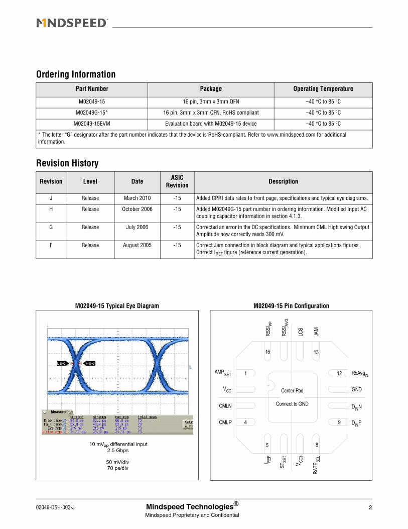
3.2.8 Average Received Signal Strength Indicator (RSSIAVG)The RSSIAVG output current is a mirrored version of the RxAVGIN current from compatible TIAs. It sources rather than sinks the current making it compatible with DDMI type interfaces.
3.2.9 Voltage RegulationThe M02049-15 contains an on-chip voltage regulator to allow both 5V and 3.3V operation. When used at 5V, the on-chip regulator is enabled and the digital inputs and outputs are compatible with TTL 5V logic levels.
Figure 3-11. RSSIAVG Output
VCC3
RSSIAVGRxAVGIN
(From TIA) REXT
VCCVCC
02049-DSH-002-J Mindspeed Technologies®19
Mindspeed Proprietary and Confidential

02049-DSH-002-J
4.0 Applications Information
4.1 Applications• 2.5 Gbps STM-16/OC-48 SDH/SONET
• 1.06, 2.12 and 4.24 Gbps Fibre Channel
• 1.25 Gbps Ethernet
• 1.25 Gbps SDH/SONET
• 2.67 Gbps SDH/SONET with FEC
4.1.1 Reference Current GenerationThe M02049-15 contains an accurate on-chip bias circuit that requires an external 12.1 kΩ 1% resistor, RREF, from pin IREF to ground to set the LOS threshold voltage at STSET precisely.
Figure 4-1. Typical Applications Diagram
optional
LevelDetect
LimitingAmplifier
ComparatorLevelShift
CMLP
CMLN
RSSIPP
RATE SEL
AMPSET
Offset cancel
OutputBuffer
ThresholdSettingCircuit Regulator
VCCSTSET VCC3
Biasing
IREFJam
LOS
RAMPSET
RST
12.1 k Ω
VTT
T I A
Photodiode
+3.3 V
DINN
RxAVGIN
RSSIAVG
DINP
AC-Coupledto TIA
REXT
MON
M02013
AC or DC Coupled(as described in
Applications Information)
Clock DataRecovery
Unit
RATESELControl
Mindspeed Technologies®20
Mindspeed Proprietary and Confidential

Applications Information
4.1.2 Connecting VCC and VCC3For 5V operation, the VCC pin is connected to an appropriate 5V ± 7.5% supply. No potential should be applied to the VCC3 pin. The only connection to VCC3 should be RST as shown in Figure 3-5.
When VCC = 5V all logic outputs and the data outputs are 5V compatible while the CML data inputs are still referenced to 3.3V from the internal regulator (see Figure 3-2). For low power operation, VCC and VCC3 should be connected to an appropriate 3.3V ± 7.5% supply. In this case all I/Os are 3.3V compatible.
4.1.3 Choosing an Input AC-Coupling CapacitorWhen AC-coupling the input, the coupling capacitor should be of sufficient value to pass the lowest frequencies of interest, bearing in mind the number of consecutive identical bits and the input resistance of the part. For SONET data, a good rule of thumb is to chose a coupling capacitor that has a cut-off frequency less than 1/(10,000) of the input data rate. For example, for 2.5 Gbps data, the coupling capacitor should be chosen as:
fCUTOFF ≤ (2.5x10⁹ / 10x103) = 250x103
The -3 dB cutoff frequency of the low pass filter at the input (TIA output R + LIA input R) is found as:
f3dB = 1/ (2 * π * (50Ω + 50Ω)* CAC)
so solving for C where f3dB = fCUTOFF
Figure 4-2. Reference Current Generation
LOSVSET
VLVL_Det
BG_Ref
VCC3
RST
RREF
STSET
IREF
02049-DSH-002-J Mindspeed Technologies®21
Mindspeed Proprietary and Confidential

Applications Information
CAC = 1/ (2 * π * 100Ω * fCUTOFF) EQ.1
and in this case the minimum capacitor is 6 nF.
For Ethernet or Fibre Channel, there are less consecutive bits in the data, and the recommended cut-off frequency is 1/(1,000) of the input data rate. This results in a minimum capacitor of less than 1 nF for 2.125 Gbps Fibre Channel.
Multirate applications down to 155 Mbps
In this case, the input coupling capacitor needs to be large enough to pass 15 kHz (155x106/10,000) which results in a capacitor value of 0.1 μF. However, because this low pass frequency is close to the 25 kHz low pass frequency of the internal DC servo loop, it is preferable to use a larger input coupling capacitor such as 1 μF which provides an input cutoff frequency of 3.1 kHz. This separates the two poles sufficiently to allow them to be considered independent. This capacitor should also have a 10 nF capacitor in parallel to pass the higher frequency data (in the multirate application) without distortion.
In all cases, a high quality coupling capacitor should be used as to pass the high frequency content of the input data stream.
4.1.4 Using Rate SelectionWhen the RATESEL pin (shown in Figure 3-10) is driven high, the M02049-15 bandwidth is set to its maximum which allows the M02049-15 to operate at data rates up to 6.144 Gbps.
Because of the nature of the ESD structure on this pin, if it is driven by a device with IOL or IOH > 2 mA then a 1 kΩ to 10 kΩ resistor should be used in series with the RATESEL pin. If rate selection is not used and the part is configured for high bandwidth only, the RATESEL pin should be connected to VCC using a 1 kΩ to 10 kΩ resistor. When operating at data rates ≤ 1.25 Gbps, then RATESEL should be left floating (do not tie low). This enables low-rate mode which reduces the bandwidth (and thus the noise level) of the part.
4.1.5 Using RSSIAVGAs shown in the typical applications circuit (Figure 4-1), when interfacing to a TIA that features a “MON” output such as the M02016 or M02013, the M02049-15 can reference the current sunk into the TIA “MON” output and produce a proportional current at the M02049-15 RSSIAVG output. The current is sourced into resistor REXT to ground creating a voltage suitable for DDMI applications. REXT should be chosen as:
REXT = 1/(maximum current into RSSIAVG)EQ.2
This keeps the voltage at RSSIAVG between 0 and 1V.
4.1.6 Setting the CML Output Swing LevelThe CML output circuit is shown in Figure 3-3. It is basically a differential pair with a tail current of ITAIL. The load of the differential pair is formed by the parallel combination of ROUT and RLOAD for high frequencies where the output AC-coupling capacitor can be considered as a short circuit (100 || 50 = 33.3 Ω). The single-ended output voltage swing is given by EQ.3:
VPP-SE = ITAIL x (ROUT || RLOAD)EQ.3
The required minimum voltage swing sets ITAIL and ITAIL determines the output power consumption. The minimum voltage swing depends on the application. Therefore, M02049-15 provides the user the flexibility to optimize the
02049-DSH-002-J Mindspeed Technologies®22
Mindspeed Proprietary and Confidential

Applications Information
voltage swing and the output power consumption for the application by setting ITAIL using an external resistor (RAMPSET) shown in Figure 4-3. To select the required swing, use the following equation (EQ.4):
ITAIL(mA) = 150 μA x ((650Ω + RAMPSET)/16Ω) EQ.4
The minimum ITAIL is 6mA and occurs when the AMPSET pin is directly connected to ground. The resulting voltage swing is approximately 200 mVpp, single-ended (= 6 mA x 33 Ω). This is sufficient for most applications. If it is necessary, the voltage swing can be increased at the expense of the power consumption by connecting an external resistor RAMPSET between the AMPSET pin and ground. The value of RAMPSET can be calculated from EQ.4. A resistor of 620 Ω results in 12 mA tail current which delivers an approximate voltage swing of ~400 mVpp, single-ended (12 mA x 33 Ω).
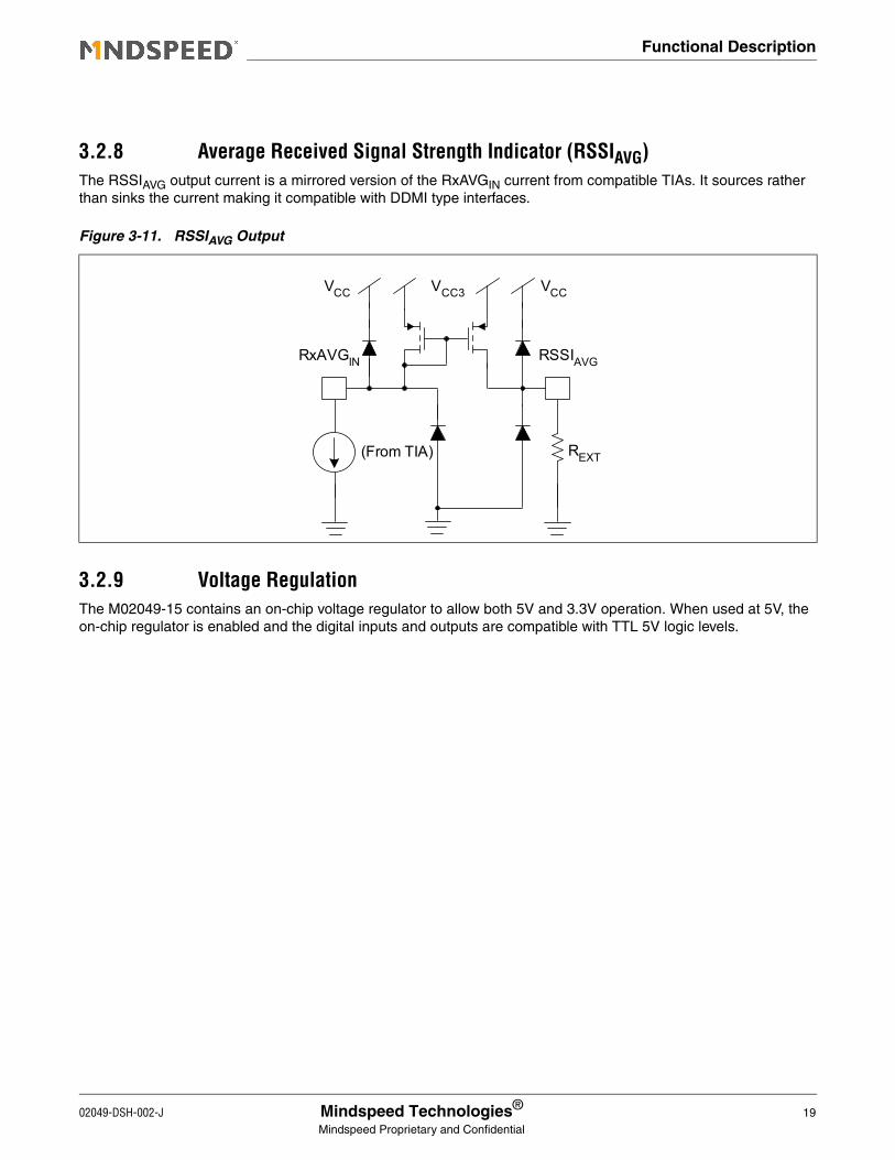
4.1.7 Setting the Signal Detect LevelUsing Figure 4-4, the value for RST is chosen to set the LOS threshold at the desired value. The resulting hysteresis is also shown in Figure 4-4.
From Figure 4-4, it is apparent that small variations in RST cause significant variation in the LOS threshold level, particularly for low input signal levels. This is because of the logarithmic relationship between the RSSI voltage and the input signal level. It is recommended that a 1% resistor be used for RST and that allowance is provided for LOS variation, particularly when the LOS threshold is near the sensitivity limit of the M02049-15.
Example RST resistor values are given in Table 4-1.
Figure 4-3. AMPset
150 µA
AMPSET
VCC
650 Ω
VAMPSET
RAMPSET
02049-DSH-002-J Mindspeed Technologies®23
Mindspeed Proprietary and Confidential

Applications Information
Table 4-1. Typical LOS Assert and De-assert Levels for Various 1% RST Resistor Values
RST (kΩ)VIN (mV pp) differential
LOS Assert LOS De-Assert
7.50 4.9 7.8
6.81 11.7 17.0
6.19 23.2 33.4
5.49 55.0 77.3
Figure 4-4. Typical Loss of Signal Characteristic (Full Input Signal Range)
RST (kΩ)
0
10
20
30
40
50
60
70
80
5.5 5.7 5.9 6.1 6.3 6.5 6.7 6.9 7.1 7.3 7.5
Thre
shol
d Le
vel (
mV PP
)
Optical Hysteresis
De-assert
Assert
= 10*log10(De-assert/Assert)
2.5 Gbps, 2 31 - 1
Conditions:
Vcc = 3.3V, Temp = 25C
02049-DSH-002-J Mindspeed Technologies®24
Mindspeed Proprietary and Confidential
Applications Information
Figure 4-5. Typical Loss of Signal Characteristic (Low Input Signal Range)
Figure 4-6. Typical Loss of Signal Characteristic (High Input Signal Range)
RST (kΩ)
0
10
20
30
6.5 6.7 6.9 7.1 7.3 7.5
Thre
shol
d Le
vel (
mV PP
)
De-assert
Assert
= 10*log10(De-assert/Assert)Optical Hysteresis
2.5 Gbps, 2 31 - 1
Conditions:
Vcc = 3.3V, Temp = 25C
Thre
shol
d Le
vel (
mV PP
)
RST (kΩ)
0
10
20
30
40
50
60
70
80
5.5 5.7 5.9 6.1 6.3 6.5
Optical Hysteresis
= 10*log10(De-assert/Assert)
Assert
De-assert
2.5 Gbps, 2 31 - 1
Conditions:
Vcc = 3.3V, Temp = 25C
02049-DSH-002-J Mindspeed Technologies®25
Mindspeed Proprietary and Confidential

Applications Information
4.1.8 Using JAMAs shown in the typical applications circuit (Figure 4-1), the LOS output pin can optionally be connected to the Jam input pin. When LOS asserts the Jam function sets the data outputs to a fixed “one” state (CMLP is held high and CMLN is held low). This is normally used to allow data to propagate only when the signal is above the users' bit error rate (BER) requirement. It prevents the outputs from toggling due to noise when no signal is present.
From the LOS assert and deassert figures above (Figure 4-4 - Figure 4-6), when an input signal is below the LOS assert threshold, LOS asserts (LOS high) causing Jam to assert. When Jam asserts, the data outputs and the internal servo loop of the M02049-15 are disabled. If the input signal reaches or exceeds the LOS deassert threshold, LOS deasserts (LOS low) causing Jam to deassert, and hence enables the data outputs and the internal servo loop. If, however, the input signal is slowly increasing to a level that does not exceed the LOS deassert threshold (operating in the hysteresis region), the internal servo loop may not be fully established and this may cause partial enabling of the data outputs. To avoid this the input signal needs to fully reach or exceed the LOS deassert level to fully enable the data outputs.
Figure 4-7. Typical Loss of Signal Hysteresis Characteristic (Full Input Signal Range)
0.0
0.5
1.0
1.5
2.0
2.5
3.0
3.5
4.0
4.5
5.0
5.5 5.7 5.9 6.1 6.3 6.5 6.7 6.9 7.1 7.3 7.5
Ele
ctric
al H
yste
resi
s (d
B)
RST (kΩ)
= 20*log10(De-assert/Assert)Electrical Hysteresis
2.5 Gbps, 2 31 - 1
Conditions:
Vcc = 3.3V, Temp = 25C
02049-DSH-002-J Mindspeed Technologies®26
Mindspeed Proprietary and Confidential
02049-DSH-002-J
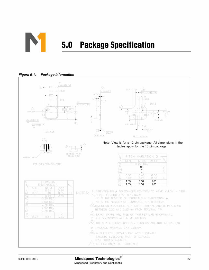
5.0 Package Specification
Figure 5-1. Package Information
Note: View is for a 12 pin package. All dimensions in thetables apply for the 16 pin package
1644
1.501.651.65
1.501.351.35
Mindspeed Technologies®27
Mindspeed Proprietary and Confidential

www.mindspeed.com
General Information:Telephone: (949) 579-3000Headquarters - Newport Beach4000 MacArthur Blvd., East TowerNewport Beach, CA 92660
© 2010 Mindspeed Technologies®, Inc. All rights reserved.
Information in this document is provided in connection with Mindspeed Technologies® ("Mindspeed®") products. These materials are provided by Mindspeed as a service to its customers and may be used for informational purposes only. Except as provided in Mindspeed’s Terms and Conditions of Sale for such products or in any separate agreement related to this document, Mindspeed assumes no liability whatsoever. Mindspeed assumes no responsibility for errors or omissions in these materials. Mindspeed may make changes to specifications and product descriptions at any time, without notice. Mindspeed makes no commitment to update the information and shall have no responsibility whatsoever for conflicts or incompatibilities arising from future changes to its specifications and product descriptions. No license, express or implied, by estoppel or otherwise, to any intellectual property rights is granted by this document.
THESE MATERIALS ARE PROVIDED "AS IS" WITHOUT WARRANTY OF ANY KIND, EITHER EXPRESS OR IMPLIED, RELATING TO SALE AND/OR USE OF MINDSPEED PRODUCTS INCLUDING LIABILITY OR WARRANTIES RELATING TO FITNESS FOR A PARTICULAR PURPOSE, CONSEQUENTIAL OR INCIDENTAL DAMAGES, MERCHANTABILITY, OR INFRINGEMENT OF ANY PATENT, COPYRIGHT OR OTHER INTELLECTUAL PROPERTY RIGHT. MINDSPEED FURTHER DOES NOT WARRANT THE ACCURACY OR COMPLETENESS OF THE INFORMATION, TEXT, GRAPHICS OR OTHER ITEMS CONTAINED WITHIN THESE MATERIALS. MINDSPEED SHALL NOT BE LIABLE FOR ANY SPECIAL, INDIRECT, INCIDENTAL, OR CONSEQUENTIAL DAMAGES, INCLUDING WITHOUT LIMITATION, LOST REVENUES OR LOST PROFITS, WHICH MAY RESULT FROM THE USE OF THESE MATERIALS.
Mindspeed products are not intended for use in medical, lifesaving or life sustaining applications. Mindspeed customers using or selling Mindspeed products for use in such applications do so at their own risk and agree to fully indemnify Mindspeed for any damages resulting from such improper use or sale.
02049-DSH-002-J Mindspeed Technologies®28
Mindspeed Proprietary and Confidential