Embed Size (px)
Citation preview

32 Gbps, Dual Channel, Advanced Linear Equalizer
Data Sheet HMC6545
Rev. B Document Feedback Information furnished by Analog Devices is believed to be accurate and reliable. However, no responsibility is assumed by Analog Devices for its use, nor for any infringements of patents or other rights of third parties that may result from its use. Specifications subject to change without notice. No license is granted by implication or otherwise under any patent or patent rights of Analog Devices. Trademarks and registered trademarks are the property of their respective owners.
One Technology Way, P.O. Box 9106, Norwood, MA 02062-9106, U.S.A.Tel: 781.329.4700 ©2015–2016 Analog Devices, Inc. All rights reserved. Technical Support www.analog.com
FEATURES Supports data rates from dc up to 32 Gbps Protocol and data rate agnostic Low latency (<170 ps) Integrated AGC with differential sensitivity of <50 mV Up to 20 dB programmable multiple unit interval input
equalization Extended chromatic and polarization mode dispersion
tolerance Programmable differential output amplitude control of up to
600 mV Single 3.3 V supply eliminating external regulators Wide temperature range from −40°C to +95°C 5 mm × 5 mm, 32-lead LFCSP package
APPLICATIONS 40 Gbps/100 Gbps DQPSK direct detection receivers Short and long reach CFP2 and QSFP+ modules CEI-28G MR and CEI-25G LR 100 GE line cards 16 Gbps and 32 Gbps Fibre Channel Infiniband 14 Gbps FDR and 28 Gbps EDR rates Signal conditioning for backplane and line cards Broadband test and measurement equipment
FUNCTIONAL BLOCK DIAGRAM
17
1
3
4
2
9
GND
INP0
INN0
GND
5
6
GND
INP1
7INN1
8GND GND
PACKAGEBASE
GND
18 OUTN1
19 OUTP1
20 GND
21 GND
22 OUTN0
23 OUTP0
24 GND
CA
GC
1
12C
OM
PN
1
11C
OM
PP
1
10V
CC
1
13S
DA
14S
CL
15S
VC
C
16V
CC
125
VC
C0
26R
EG
SE
L0
27R
EG
SE
L1
28R
ST
29C
OM
PN
0
30C
OM
PP
0
31V
CC
0
32C
AG
C0
AGC
T/2
c0
T/2
c1
T/2
c2
T/2
T/2 T/2 T/2 T/2
cn
d0 d1 d2 dn
AGC
LPF
LPF
SERIAL CONTROLREGISTERS
Σ
Σ
HMC6545
1339
3-00
1
Figure 1.
GENERAL DESCRIPTION The HMC6545 is a low power, high performance, fully programmable, dual-channel, asynchronous advanced linear equalizer that operates at data rates of up to 32 Gbps. The HMC6545 is protocol and data rate agnostic, and it can operate on the transmit path to predistort a transmitted signal to invert channel distortion or on the receiver path to equalize the distorted and attenuated received signal. The HMC6545 is effective in dealing with chromatic and polarization mode dispersion and intersymbol interference (ISI) caused by a wide variety of transmission media (backplane or fiber) and channel lengths.
The HMC6545 consists of an automatic gain control (AGC); dc offset correction circuitry; a 9-tap, 18 ps spaced feedforward equalizer (FFE); a summing node; and a linear programmable output driver. The input AGC linearly attenuates or amplifies the distorted input signal to generate a constant voltage at the
input of the FFE. The 9-tap FFE is programmed via 2-wire interface to generate wide range frequency responses that are precursor or postcursor in nature for compensating signal impairments. After FFE tap coefficients are summed at the summing node, the signal is received by a linear output driver. DC offset correction circuitry is controlled either automatically or manually via Forward Error Correction (FEC).
All high speed differential inputs and outputs of the HMC6545 are current mode logic (CML) and terminated on chip with 50 Ω to the positive supply, 3.3 V, and can be dc-coupled or ac-coupled. The inputs and outputs of the HMC6545 can be operated either differentially or single-ended. The low power, high performance, and feature rich HMC6545 is packaged in a 5 mm × 5 mm, 32-lead LFCSP package. The device uses a single 3.3 V supply, eliminating external regulators. The HMC6545 operates over a −40°C to +95°C temperature range.

HMC6545 Data Sheet
Rev. B | Page 2 of 23
TABLE OF CONTENTS Features .............................................................................................. 1
Applications ....................................................................................... 1
Functional Block Diagram .............................................................. 1
General Description ......................................................................... 1
Revision History ............................................................................... 2
Specifications ..................................................................................... 3
DC Electrical Characteristics ...................................................... 3
AC Electrical Characteristics ...................................................... 3
Absolute Maximum Ratings ............................................................ 5
ESD Caution .................................................................................. 5
Pin Configuration and Function Descriptions ............................. 6
Interface Schematics..................................................................... 7
Typical Performance Characteristics ..............................................8
Theory of Operation ...................................................................... 11
Input Receiver ............................................................................. 11
FFE Delay Line ........................................................................... 11
Output Driver ............................................................................. 12
2-Wire Serial Port ....................................................................... 12
Register Map ................................................................................... 15
Register List Summary and Register Descriptions ................ 15
Evaluation Printed Circuit Board (PCB) ..................................... 21
Evaluation Kit Contents ............................................................ 21
Outline Dimensions ....................................................................... 23
Ordering Guide .......................................................................... 23
REVISION HISTORY 6/2016—Rev. A to Rev. B Changes to Table 6 .......................................................................... 12 Changes to Table 13 ........................................................................ 15 Changes to Figure 35 ...................................................................... 22 10/2015—Revision A: Initial Version

Data Sheet HMC6545
Rev. B | Page 3 of 23
SPECIFICATIONS DC ELECTRICAL CHARACTERISTICS Unless otherwise noted, typical values at VCC = 3.3 V, TA = 25°C.
Table 1. Parameter Symbol Test Conditions/Comments Min Typ Max Unit POWER CONSUMPTION
Supply Voltage VCC 3.00 3.30 3.45 V Supply Current ICCMAX Single channel; all tap amplifiers active 130 150 mA ICCMIN Single channel; single-tap amplifier active 93 mA Power-Down Supply Current 17 mA DC Offset Correction At maximum AGC gain
Automatic −60 +60 mV Manual −60 +60 mV
CML INPUT PORT (INP0, INN0, INP1, INN1) Input Termination RIN Differential input resistance 80 100 120 Ω
CML OUTPUT PORT (OUTP0, OUTN0, OUTP1, OUTN1)
Output Termination ROUT Single-ended output resistance 45 55 65 Ω Output Level
High VOH VCC V Output VOL VCC − 0.5 V
CMOS INPUT (SDA, SCL, RST, REGSEL0, REGSEL1)
Input Voltage Level High VIH VCC − 1.3 V Input VIL 0.8 V
Input Current IIL, IIH VIL = 0 V or VIH = VCC −100 +100 µA
AC ELECTRICAL CHARACTERISTICS Unless otherwise noted, typical values at VCC = 3.3 V, TA = 25°C.
Table 2. Parameter Test Conditions/Comments Min Typ Max Unit INPUT
Data Rate DC 32 Gbps Range Differential input range for linear AGC operation, THD < 5% 40 880 mV p-p Input Equalization 20 dB
DIFFERENTIAL AMPLITUDE Input 40 1600 mV p-p Output Input signal: PRBS 231 − 1 at 100 mV p-p
Linear AGC Operation THD < 5%; AGC = 2; all taps enabled, Tap 4 gain = 63, gain of all other taps = 0, predriver gain = 63
410 mV p-p
AGC = 7 600 mV p-p Saturated AGC Operation All taps are enabled with maximum gain, predriver gain = 63, AGC = 7 960 mV p-p
AGC SETTLING TIME No external capacitor 0.5 µs FFE
Tap Delay 18 ps Delay Depth 145 ps

HMC6545 Data Sheet
Rev. B | Page 4 of 23
Parameter Test Conditions/Comments Min Typ Max Unit NOISE CHARACTERISTICS
Channel to Channel Isolation Up to 32 GHz 30 dB Total Harmonic Distortion AGC = 2, for differential input voltage ≤ 250 mV p-p 5 % Output Driver Rise/Fall Time 20% to 80% 16 ps Additive RMS Jitter1 Input signal: 28 Gbps, 1010 pattern; all taps enabled, Tap 4 gain = 63,
gain of all other taps = 0, predriver gain = 63; AGC = 2 0.4 ps
LATENCY 170 ps DIFFERENTIAL RETURN LOSS Up to 20 GHz
Input −9 dB Output −8 dB
NUMBER OF TAPS 9 1 Additive rms jitter is calculated by JRMS,DUT = √((JTESTED)2 − (JSOURCE)2).

Data Sheet HMC6545
Rev. B | Page 5 of 23
ABSOLUTE MAXIMUM RATINGS Table 3. Parameter Rating VCC to GND −0.6 V to +3.6 V All Pins to GND −0.3 V to VCC + 0.3 V Operating Ambient Temperature Range −40°C to +95°C Differential Peak-to-Peak Input Voltage
Swing 1.6 V p-p
Maximum Input Voltage at CML Inputs VCC + 0.6 V Maximum Input Voltage at Digital Inputs (SDA, SCL, REGSEL1, REGSEL0, RST)
VCC + 0.6 V
Maximum Peak Reflow Temperature (MSL1)1 260°C Maximum Junction Temperature 125°C Continuous Power Dissipation (TA = 85°C,
Derate 46.59 mW/°C Above 85°C) 1.86 W
Thermal Resistance (Junction to EPAD) 21.46°C/W ESD Sensitivity, Human Body Model (HBM) Class 1C
1 See the Ordering Guide section.
Stresses at or above those listed under Absolute Maximum Ratings may cause permanent damage to the product. This is a stress rating only; functional operation of the product at these or any other conditions above those indicated in the operational section of this specification is not implied. Operation beyond the maximum operating conditions for extended periods may affect product reliability.
ESD CAUTION

HMC6545 Data Sheet
Rev. B | Page 6 of 23
PIN CONFIGURATION AND FUNCTION DESCRIPTIONS
17
1
3
4
2
9
GND
INP0
INN0
GND
5
6
GND
INP1
7INN1
8GND GND
PACKAGEBASE
GND
18 OUTN1
19 OUTP1
20 GND
21 GND
22 OUTN0
23 OUTP0
24 GND
CA
GC
1
12C
OM
PN
1
11C
OM
PP
1
10V
CC
1
13S
DA
14S
CL
15S
VC
C
16V
CC
125
VC
C0
26R
EG
SE
L0
27R
EG
SE
L1
28R
ST
29C
OM
PN
0
30C
OM
PP
0
31V
CC
0
32C
AG
C0
HMC6545TOP VIEW
(Not to Scale)
NOTES1. EXPOSED PAD. EXPOSED PAD MUST
BE CONNECTED TO RF/DC GROUND. 1339
3-03
3
Figure 2. Pin Configuration
Table 4. Pin Function Descriptions Pin Number Mnemonic Description 1, 4, 5, 8, 17, 20, 21, 24 GND Ground. This pin and the package base must be connected to RF and dc ground. 2, 3 INP0, INN0 Differential CML Inputs, Channel 0. 6, 7 INP1, INN1 Differential CML Inputs, Channel 1. 9, 32 CAGC1, CAGC0 External Capacitor for AGC Bandwidth. 10, 16 VCC1 Power Supplies for Channel 1. 11, 12 COMPP1, COMPN1 External Capacitors to Cancel DC Offset, Channel 1. 13 SDA 2-Wire Digital Data. 14 SCL 2-Wire Digital Clock. 15 SVCC Power Supply for Digital Circuitry and Bias. 18, 19 OUTN1, OUTP1 Differential CML Data Outputs, Channel 1. 22, 23 OUTN0, OUTP0 Differential CML Data Outputs, Channel 0. 25, 31 VCC0 Power Supplies for Channel 0. 29, 30 COMPN0, COMPP0 External Capacitors to Cancel DC Offset, Channel 0. 26, 27 REGSEL0, REGSEL1 Default Coefficient Selection for Channel and 2-Wire Interface Device Address. 28 RST Reset for 2-Wire Interface.
EPAD Exposed Pad. The exposed pad must be connected to RF/dc ground.
Data Sheet HMC6545
Rev. B | Page 7 of 23
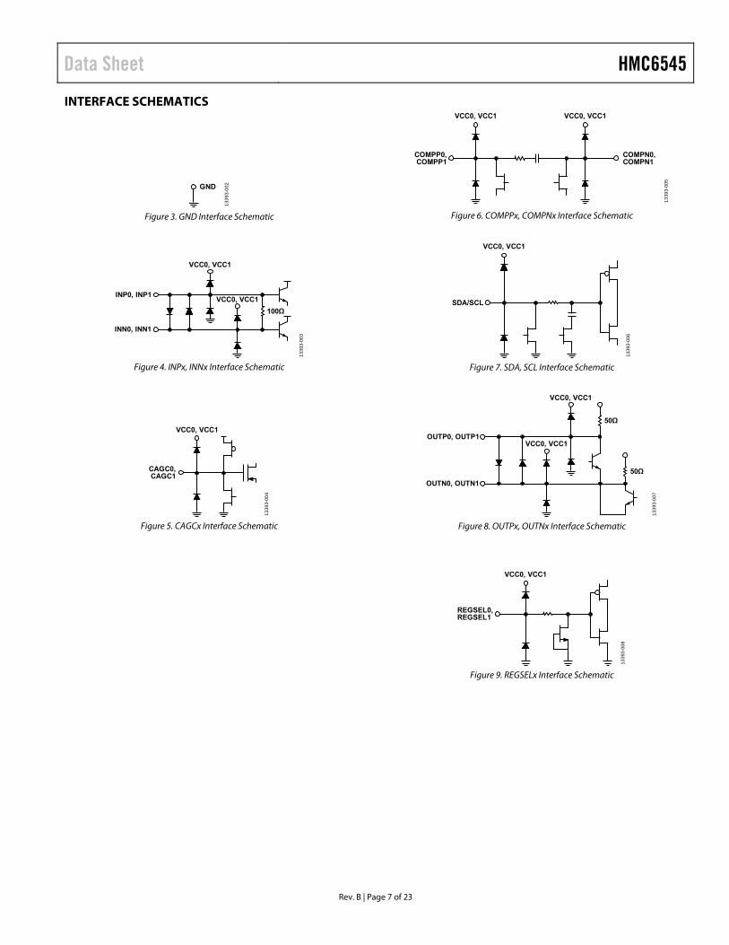
INTERFACE SCHEMATICS
GND
1339
3-00
2
Figure 3. GND Interface Schematic
100Ω
VCC0, VCC1
VCC0, VCC1INP0, INP1
INN0, INN1
1339
3-00
3
Figure 4. INPx, INNx Interface Schematic
CAGC0,CAGC1
VCC0, VCC1
1339
3-00
4
Figure 5. CAGCx Interface Schematic
VCC0, VCC1 VCC0, VCC1
COMPP0,COMPP1
COMPN0,COMPN1
1339
3-00
5
Figure 6. COMPPx, COMPNx Interface Schematic
VCC0, VCC1
SDA/SCL
1339
3-00
6
Figure 7. SDA, SCL Interface Schematic
VCC0, VCC1
VCC0, VCC1OUTP0, OUTP1
OUTN0, OUTN1
50Ω
50Ω
1339
3-00
7
Figure 8. OUTPx, OUTNx Interface Schematic
VCC0, VCC1
REGSEL0,REGSEL1
1339
3-00
8
Figure 9. REGSELx Interface Schematic

HMC6545 Data Sheet
Rev. B | Page 8 of 23
TYPICAL PERFORMANCE CHARACTERISTICS 150
80
90
100
120
140
110
130
0 1 2 3 4 6 85 7 9
I DD
(m
A)
ENABLED TAPS
3.00V3.15V3.30V3.45V
1339
3-00
9
TA = 25°C
Figure 10. Supply Current (IDD) vs. Enabled Taps Over Supply Voltage
300
250
200
150
100
500 1 2 3 4 6 85 7 9
I DD
(m
A)
ENABLED TAPS
CHANNEL 0CHANNEL 0 + CHANNEL 1
1339
3-01
0
TA = 25°CVCC = 3.3VAGC = 3PREDRIVER GAIN = 63
Figure 11. Supply Current (IDD) vs. Enabled Taps Over Enabled Channels
1.0
–1.0
–0.6
–0.2
0.4
0.8
0.2
–0.8
–0.4
0
0.6
–63
–56
–49
–42
–35
–28
–21
–14 –7 0 7 14 21 28 35 42 49 56 63
LIN
EA
RIT
Y (
V/V
)
TAP VALUE
+95°C+25°C–40°C
1339
3-01
1
VCC = 3.3VAGC = 3PREDRIVER GAIN = 63
Figure 12. Normalized Linearity vs. Tap Value Over Temperature, Tap 4 Value Is Varied, While Others Are Enabled with No Gain
140
80
90
100
120
110
130
0 1 2 3 4 6 85 7 9
I DD
(m
A)
ENABLED TAPS
+95°C+25°C–40°C
1339
3-01
2
VCC = 3.3V
Figure 13. Supply Current vs. Enabled Taps Over Temperature
1.0
–1.0
–0.6
–0.2
0.4
0.8
0.2
–0.8
–0.4
0
0.6
–63
–56
–49
–42
–35
–28
–21
–14 –7 0 7 14 21 28 35 42 49 56 63
LIN
EA
RIT
Y (
V/V
)
TAP VALUE
3.00V3.15V3.30V3.45V
1339
3-01
3
TA = 25°CAGC = 3PREDRIVER GAIN = 63
Figure 14. Normalized Linearity vs. Tap Value Over Supply Voltage, Tap 4 Value Is Varied, While Others Are Enabled with No Gain
12
0
2
4
8
6
10
25 75 125 175 225 375 575275 475325 525425 625
TH
D (
%)
DIFFERENTIAL INPUT AMPLITUDE (mV p-p)
3.15V3.30V3.45V
1339
3-01
4
TA = 25°CAGC = 2PREDRIVER GAIN = 63
Figure 15. THD vs. Differential Input Amplitude Over Supply Voltage, Tap 4 Gain Is Set to +63, While Others are Enabled with No Gain

Data Sheet HMC6545
Rev. B | Page 9 of 23
12
0
2
4
8
6
10
25 75 125 175 225 375 575275 475325 525425 625
TH
D (
%)
DIFFERENTIAL INPUT AMPLITUDE (mV p-p)
+95°C+25°C–40°C
1339
3-01
5
VCC = 3.3VAGC = 2PREDRIVER GAIN = 63
Figure 16. THD vs. Differential Input Amplitude Over Temperature, Tap 4 Gain Is Set to Maximum Gain, While Others Are Enabled with No Gain
7
0
1
2
4
3
5
6
0 7 14 21 28 4935 42 56 63
TH
D (
%)
PREDRIVER GAIN 1339
3-01
6TA = 25°CVCC = 3.3VAGC = 2
Figure 17. THD vs. Predriver Gain, Tap 4 Gain Is Set to Maximum Gain, While Others Are Enabled with No Gain
20
–20
–16
–12
4
–4
12
–8
8
0
16
0 2 6 10 14 2618 224 8 12 16 20 24 28 30
SM
AL
L S
IGN
AL
GA
IN (
dB
)
FREQUENCY (GHz)
TAP 0TAP 1TAP 2TAP 3TAP 4TAP 5TAP 6TAP 7TAP 8
1339
3-01
7
TA = 25°CVCC = 3.3V
Figure 18. Small Signal Gain Over Taps, for S21 Line of Each Tap, Relevant Tap Is Set to Maximum Gain While Remaining Taps Are Enabled with No
Gain
12
0
2
4
8
6
10
25 75 125 175 225 375 575275 475325 525425 625
TH
D (
%)
DIFFERENTIAL INPUT AMPLITUDE (mV p-p)
AGC = 2AGC = 3
1339
3-01
8
TA = 25°CVCC = 3.3VPREDRIVER GAIN = 63
Figure 19. THD vs. Differential Input Amplitude Over AGC Value, Tap 4 Gain Is Set to Maximum Gain, While Others Are Enabled with No Gain
900
0
100
200
400
300
500
700
600
800
0 7 14 21 28 4935 42 56 63
DIF
FE
RE
NT
IAL
OU
TP
UT
AM
PL
ITU
DE
(m
V p
-p)
PREDRIVER GAIN SETTING
AGC = 0AGC = 4AGC = 7
1339
3-01
9
TA = 25°CVCC = 3.3VAGC = 4PREDRIVER GAIN = 7
TAP 0 = –3TAP 1 = –8TAP 2 = –4TAP 3 = +63TAP 4 = +63TAP 5 = +57TAP 6 = +18TAP 7 = –41TAP 8 = –35
Figure 20. Differential Output Amplitude vs. Predriver Gain Over AGC, Input Signal: Differential PRBS 231 − 1, 10 Gbps at 500 mV p-p
0
–30
–25
–20
–10
–15
–5
0 2 6 10 14 2618 224 8 12 16 20 24 28 30
INP
UT
RE
TU
RN
LO
SS
(d
B)
FREQUENCY (GHz) 1339
3-02
0
TA = 25°CVCC = 3.3V
Figure 21. Input Return Loss

HMC6545 Data Sheet
Rev. B | Page 10 of 23
0
–30
–25
–20
–10
–5
–15
0 2 6 10 14 2618 224 8 12 16 20 24 28 30
OU
TP
UT
RE
TU
RN
LO
SS
(d
B)
FREQUENCY (GHz) 1339
3-02
1
TA = 25°CVCC = 3.3V
Figure 22. Output Return Loss
CH3 100mV/DIV TIME 10ps/DIV DELAY 24.1475ns
CURRENT MINIMUM MAXIMUM TOTAL MEASJITTER RMS (F1) 944 fS 944 fS 982 fS 94JITTER p-p (F1) 5.444ps 5.333ps 5.444ps 94RISE TIME (F1) 16.22ps 18.22ps 18.44ps 94FALL TIME (F1) 16.22ps 16.00ps 18.67ps 94
1339
3-02
2
TAP 0 = –3TAP 1 = +63TAP 2 = –10TAP 3 = +4TAP 4 = –1
TAP 5 = –1TAP 6 = –1TAP 7 = –1TAP 8 = –2
AGC = 4PREDRIVER GAIN = 63
Figure 23. Typical Output Waveform at 22 Gbps, PRBS 231 − 1 Input Data, Input Signal = 300 mV p-p Differential
CH3 100mV/DIV TIME 10ps/DIV DELAY 24.1112ns
CURRENT MINIMUM MAXIMUM TOTAL MEASJITTER RMS (F1) 1.053ps 1.025ps 1.080ps 125JITTER p-p (F1) 5.557ps 5.333ps 5.567ps 125RISE TIME (F1) 17.93ps 10.00ps 17.33ps 125FALL TIME (F1) 17.11ps 16.44ps 17.33ps 125
1339
3-02
3
TAP 0 = –3TAP 1 = +63TAP 2 = –10TAP 3 = +4TAP 4 = –1
TAP 5 = –1TAP 6 = –1TAP 7 = –1TAP 8 = –2
AGC = 4PREDRIVER GAIN = 63
Figure 24. Typical Output Waveform t 28 Gbps, PRBS 231 − 1 Input Data
CH3 100mV/DIV TIME 10ps/DIV DELAY 24.2003ns
CURRENT MINIMUM MAXIMUM TOTAL MEASJITTER RMS (F1) 914 fS 948 fS 4.014ps 236JITTER p-p (F1) 4.880ps 4.000ps 4.889ps 236RISE TIME (F1) 16.22ps 16.22ps 16.67ps 236FALL TIME (F1) 18.22ps 17.78ps 16.67ps 236
1339
3-02
4
TAP 0 = –3TAP 1 = +63TAP 2 = –10TAP 3 = +4TAP 4 = –1
TAP 5 = –1TAP 6 = –1TAP 7 = –1TAP 8 = –2
AGC = 4PREDRIVER GAIN = 63
Figure 25. Typical Output Waveform at 10 Gbps PRBS 231 − 1 Input Data
CH3 100mV/DIV TIME 10ps/DIV DELAY 24.1468ns
CURRENT MINIMUM MAXIMUM TOTAL MEASJITTER RMS (F1) 1.008ps 994 fS 1.021ps 66JITTER p-p (F1) 5.557ps 5.333ps 5.557ps 66RISE TIME (F1) 17.11ps 16.07ps 17.11ps 66FALL TIME (F1) 16.69ps 16.44ps 17.11ps 66
1339
3-02
5
TAP 0 = –3TAP 1 = +63TAP 2 = –10TAP 3 = +4TAP 4 = –1
TAP 5 = –1TAP 6 = –1TAP 7 = –1TAP 8 = –2
AGC = 4PREDRIVER GAIN = 63
Figure 26. Typical Output Waveform at 25.8 Gbps, PRBS 231 − 1 Input Data
CH3 100mV/DIV TIME 10ps/DIV DELAY 24.0976ns
CURRENT MINIMUM MAXIMUM TOTAL MEASJITTER RMS (F1) 960 fS 957 fS 1.036ps 100JITTER p-p (F1) 5.557ps 5.333ps 5.557ps 100RISE TIME (F1) 15.78ps 15.56ps 15.78ps 100FALL TIME (F1) 15.56ps 15.56ps 16.08ps 100
1339
3-02
6
TAP 0 = –3TAP 1 = +63TAP 2 = –10TAP 3 = +4TAP 4 = –1
TAP 5 = –1TAP 6 = –1TAP 7 = –1TAP 8 = –2
AGC = 4PREDRIVER GAIN = 63
Figure 27. Typical Output Waveform at 32 Gbps, PRBS 231 − 1 Input Data

Data Sheet HMC6545
Rev. B | Page 11 of 23
THEORY OF OPERATION The HMC6545 advanced linear equalizer has two symmetrical channels, each containing an input AGC, a 9-tap delay chain with each delay tap connected to a variable tap amplifier, a summation node combining the outputs of the tap amplifiers, and an output driver.
INPUT RECEIVER AGC
The HMC6545 has an integrated AGC that linearly amplifies/ attenuates the input signal, generating a fixed voltage swing level for further processing in the FFE delay line. An input AGC is required both to supply a well defined voltage swing level to the FFE delay line and to control the internal and external (output) voltage swings because the signal path is linear. The AGC has a sensitivity level of 40 mV p-p differential. The HMC6545 processes the input signal linearly at up to a 600 mV p-p differential input voltage level.
The AGC loop bandwidth and settling time can be changed using an external capacitor connected to the CAGC0/GND and CAGC1/GND nodes. An internal 2.5 pF capacitor at these nodes sets the default AGC settling time to 0.5 µs. The evaluation board includes 1 nF capacitors for both channels.
Internal and External Offset Correction Circuitry
The input receiver has two modes of offset correction that can be configured by changing the offset settings register via the 2-wire interface: automatic offset correction and manual offset correction (all registers in Table 5 are identical to each other).
Table 5. Offset Settings Registers Register Description Register 0x0A Channel 0 Offset Settings, Array A register Register 0x2A Channel 0 Offset Settings, Array B register Register 0x4A Channel 1 Offset Settings, Array A register Register 0x6A Channel 1 Offset Settings, Array B register
By default, the input receiver is configured in the automatic offset correction mode, which can correct up to ±60 mV of input referred dc offset at the worst case AGC gain (maximum AGC gain with a minimum input signal level). The input referred automatic offset correction range changes depending on the AGC gain and increases up to ±180 mV for minimum AGC gain with a maximum signal level at the input of the receiver.
Automatic offset correction loop bandwidth is externally set by a series RC network (for each channel, R1/C1 and R2/C2), and it is recommended to keep the component values as shown in the evaluation board schematic (see Figure 35).
For Channel 1, Array A, automatic offset correction loop can be disabled by setting Register 0x4A, Bit 6 to 0, which enables the manual offset correction (set Register 0x0A for Channel 0, Array A; Register 0x2A for Channel 0, Array B; and Register 0x6A for Channel 1, Array B; see Table 5). Manual offset correction
amount can be adjusted by configuring Register 0x4A, Bits[5:0], where Register 0x4A, Bit 5 defines the sign and Bits[4:0] define the magnitude of gain (see Table 48). Similar to automatic offset correction mode, manual offset correction dynamic range changes with the AGC gain with the total correction being ±60 mV for maximum AGC gain, which corresponds to about 2 mV/step (5-bit control) adjustment resolution for maximum AGC gain. For minimum AGC gain, the correction dynamic range increases to ±180 mV, and the minimum step for adjustment increases to 6 mV/step.
FFE DELAY LINE The FFE delay line receives an input signal from the AGC (with a controlled magnitude), and this signal propagates along a delay line composed of eight delay elements, where each delay element has 18 ps nominal propagation. The delayed signals are then multiplied by programmable coefficients by the tap amplifiers and summed together. One of the taps near the center can be selected as the main tap. The taps that follow are called postcursor taps, and the taps that precede are called precursor taps.
By combining different tap values, a wide variety of filter transfer functions can be created that can, for example, compensate for the gain or phase distortion of a lossy channel or the chromatic dispersion of an optical channel.
Tap amplifier gains are controlled using the 2-wire interface with five bits of magnitude resolution with positive or negative polarity. To disable a coefficient, set the gain of the particular tap amplifier to 0 (positive gain sign, and 0 gain setting). In addition, the tap amplifier can be powered down to save power, but this may have an impact on the delay and gain of the remaining taps in the delay chain. See Table 14 to Table 22 and Table 38 to Table 46 for Array A tap amplifier settings for Channel 0 and Channel 1, respectively. For Array B tap amplifier settings, see Table 26 to Table 34 and Table 50 to Table 58 for Channel 0 and Channel 1, respectively.
Each channel has two sets of tap coefficient register arrays (Channel 0, Array A; Channel 0, Array B; Channel 1, Array A; and Channel 1, Array B) that can be configured through the 2-wire interface. Register 0x00 to Register 0x08 set the tap coefficients of Channel 0, Array A. Register 0x20 to Register 0x28 set the tap coefficients of Channel 0, Array B. Register 0x40 to Register 0x48 set the tap coefficients of Channel 1, Array A. Register 0x60 to Register 0x68 set the tap coefficients of Channel 1, Array B. The REGSEL0 and REGSEL1 pins of the device set the default register array (A or B), determining the tap coefficients of a particular channel. For example, applying REGSEL0 = 0 activates Channel 0, Array A; and REGSEL1 = 0 activates Channel 1, Array A. Applying REGSEL0 = 1 activates Channel 0, Array B; and REGSEL1 = 1 activates Channel 1, Array B.

HMC6545 Data Sheet
Rev. B | Page 12 of 23
OUTPUT DRIVER After the tap amplifier outputs are summed, the combined signal is received by a linear output driver. The output driver consists of two stages. The first stage is a predriver stage providing controllable signal amplification (6-bit resolution) using Register 0x09 (Channel 0, Array A), Register 0x29 (Channel 0, Array B), Register 0x49 (Channel 1, Array A), and Register 0x69 (Channel 1, Array B). Similar to the tap coefficient registers, each predriver has two registers that can be selected asynchro-nously by the REGSEL0 and REGSEL1 pins. The register values must be configured through the 2-wire interface prior to the register selection via the REGSEL0 and REGSEL1 pins.
See Table 7 to Table 10 for the predriver settings for Channel 0 and Channel 1.
The final stage of the output driver is a 50 Ω CML driver stage that provides the specified linearity (according to the THD specification) up to 600 mV p-p differential output swing. The linearity degrades at higher output swings.
2-WIRE SERIAL PORT To access all of its internal registers, the HMC6545 uses a 2-wire interface, which consists of a serial data line (SDA) and a serial clock line (SCL). Both SDA and SCL are implemented with open-drain input/output pins and are connected to a positive supply voltage via pull-up resistors.
Typically, a microcontroller, a microprocessor or a digital signal processor acts as a master, controls the bus, and has the responsibil-ity to generate the clock signal and device addresses.
The HMC6545 functions as a slave device. The device address on the HMC6545 is 0x38 (default) and set by connecting the REGSEL0 and REGSEL1 pins to either VCC (Logic 1) or GND (Logic 0) and by writing 1 to Register 0x80, Bit 6. If Register 0x80, Bit 6 = 0 (default), the REGSEL0 and REGSEL1 pins select Array A or Array B. If Register 0x80, Bit 6 = 1, the REGSEL0 and REGSEL1 pins also determine the 2-wire interface device address according to Table 6.
Table 6. 2-Wire Interface Device Address Setting
REGSEL1 REGSEL0 Address Setting (Register 0x80, Bit 6 = 1)
0 0 0x38 (default) 0 1 0x3A 1 0 0x3C 1 1 0x3E
Table 7. Register 0x09—Channel 0 Predriver Settings, Array A Register Bits Type Name Default Minimum Maximum Description [5:0] R/W Predriver gain 0x30 000000 111111 Channel 0 predriver gain [7:6] R/W Factory set 0b00 Not used
Table 8. Register 0x29—Channel 0 Predriver Settings, Array B Register Bits Type Name Default Minimum Maximum Description [5:0] R/W Predriver gain 0x3F 000000 111111 Channel 0 predriver gain [7:6] R/W Factory set 0b00 Not used
Table 9. Register 0x49—Channel 1 Predriver Settings, Array A Register Bits Type Name Default Minimum Maximum Description [5:0] R/W Predriver gain 0x30 000000 111111 Channel 1 predriver gain [7:6] R/W Factory set 0b00 Not used
Table 10. Register 0x69—Channel 1 Predriver Settings, Array B Register Bits Type Name Default Minimum Maximum Description [5:0] R/W Predriver gain 0x3F 000000 111111 Channel 1 predriver gain [7:6] R/W Factory set 0b00 Not used

Data Sheet HMC6545
Rev. B | Page 13 of 23
Protocol
Table 11 lists the definitions and conditions occurring in a 2-wire data transfer.
Figure 28 shows a representation of a complete communication cycle on the 2-wire interface.
The master generates a start condition to indicate the beginning of a new data transfer.
The master then starts generating clock pulses on SCL and transmits the first byte on SDA. This first byte always consists of a 7-bit slave address followed by one bit that indicates the read/ write direction (R/W). The device on the bus with a matching address generates an acknowledge.
The master continues generating more clock pulses on SCL and, depending on the value of the R/W bit, sends (write operation, R/W = 0) or receives (read operation, R/W = 1) data on SDA. In each case, the receiver must acknowledge the data sent by the transmitter. This sequence of 8-bit data followed by a 1-bit acknowledge can be repeated multiple times.
When all data communication is over for the current transfer cycle, the master indicates the end of data transfer by generating a stop condition.
Data Transfer Formats
Write Cycle
In a write cycle, the master transmitter sends data to the slave receiver. The transfer direction is from master to slave and does not change (see Figure 29). The master generates a start condition followed by a 7-bit slave address and by the R/W bit set to 0. The slave with a matching address replies with an acknowledge. The master then transmits the first byte to the slave device. This first byte is an address of the internal registers of the slave. The slave device replies with an acknowledge bit. For a subsequent read cycle, the master generates a stop bit; otherwise, the master then transmits the next byte, which is a data byte to be stored in the internal slave register previously addressed. This data byte is followed by an acknowledge bit from the slave. This process can continue for multiple bytes, and the slave device increments its internal register address count as it receives subsequent bytes from the master. When all data transfer is over, the master generates a stop condition to end the cycle.
Table 11. 2-Wire Data Transfer Terminology and Definitions Term Definition Start A start condition is always generated by the master and is defined as a high to low transition on the SDA line while
SCL is high. The bus becomes busy after a start condition. Stop A stop condition is always generated by the master and is defined as a low to high transition on the SDA line while
SCL is high. The bus becomes free after the stop condition occurs. Byte Format Every byte transmitted on SDA must be eight bits long and is transferred with the most significant bit (MSB) first.
Each byte must be followed by an acknowledge bit. Data Valid Condition For data to be considered valid, the SDA line must be stable during the entire high period of its respective clock pulse. Acknowledge For each byte sent or received on the bus, the master generates an extra clock cycle that is used for acknowledgement,
for a total of nine bits. The transmitter releases the SDA line, which is pulled high by the external resistor, and the receiver must pull down the SDA line and drive it low while SCL is high during this entire clock cycle to indicate acknowledgment. SDA is left high during this clock cycle to indicate a no acknowledge (NACK) situation, usually because the device addressed is unable to receive or transmit the data requested.
1 2 7 8 9 7 8 91 2 7 8 91 2
SDA
SCL
STARTCONDITION
STOPCONDITION
MSB
ADDRESS DATAACK ACK DATA ACKR/W
1339
3-02
7
Figure 28. Complete Data Transfer
START R/W = 0 ACK ACK STOPNACKDATA BYTEACK ADDRESS BYTE DATA BYTESLAVE ADDRESS
FROM MASTER TO SLAVE FROM SLAVE TO MASTER 1339
3-02
8
Figure 29. Write Cycle

HMC6545 Data Sheet
Rev. B | Page 14 of 23
Read Cycle
In a read cycle, the master reads from the slave immediately after the first byte. The direction of data transfer changes between master and slave (see Figure 32). In this case, the R/W bit is set to 1 to indicate that the master reads data from the slave device. The address of the internal register from which the data is to come has been previously set in a precedent write cycle; otherwise, the slave device defaults to Address 0x00. This time, the slave device transmits all the data bytes and the master replies with an acknowledge bit. For the last byte read, the master replies with a no acknowledge bit to indicate to the slave that it must stop transmitting data. The master then generates a stop condition, and the cycle ends.
2-Wire Interface Design Considerations
The HMC6545 2-wire interface slave interface responds to any register address or data matching its chip address even when there is no preceding start condition. A 2-wire interface communication is defined as shown in Figure 30.
1339
3-03
4
START CHIP ADDRESS + WRITE ADDRESS BYTE DATA BYTE STOP
START CHIP ADDRESS + READ DATA BYTE STOP Figure 30. 2-Wire Interface Communication
Coincidentally, the data or register address can be the same as the chip address of another device on the same bus. However,
that other device does not respond because there is no preceding start condition.
In the HMC6545, regardless of whether there is a start condition, if the HMC6545 sees a bit stream that corresponds to its chip address, it then responds and causes unwanted results.
There must be only one HMC6545 device on the 2-wire interface bus; otherwise, 2-wire interface bus multiplexers can be used to isolate the HMC6545 devices. See Figure 33 for an example design.
Reset
A low strobe signal must be sent to the RST pin to reset the registers to their default values. SDA and SCL must be high in the 2-wire interface bus before and after the rising edge.
SDA
SCL
RST
0.5µs 0.5µs
1.0µs 1339
3-03
1
Figure 31. Reset Registers
START R/W = 1 ACK ACK STOPNACKDATA BYTEACK DATA BYTE DATA BYTESLAVE ADDRESS
FROM MASTER TO SLAVE FROM SLAVE TO MASTER 1339
3-02
9
Figure 32. Read Cycle
MASTER
HMC6545
HMC65452-WIRE
INTERFACEBUS
DEMUX CONTROL
OTHER VENDORSLAVE1
OTHER VENDORSLAVE2
1339
3-03
0
2-WIREINTERFACE
BUS
2-WIREINTERFACE
BUS
Figure 33. Multiple HMC6545 Devices on 2-Wire Interface Bus

Data Sheet HMC6545
Rev. B | Page 15 of 23
REGISTER MAP REGISTER LIST SUMMARY AND REGISTER DESCRIPTIONS Global Register
Global register bit order is different for read and write operations.
Table 12. Register 0x80—Global Register, Write Operation Bit Type Name Default Description 7 W Factory set 0 Not used. 6 W 2-wire interface device
address read 0 2-wire interface device address set. Writing 1 generates a 2-wire interface device
address read command. 5 W Channel 1 enable 1 Channel 1 enable. Writing 1 enables Channel 1. 4 W Channel 0 enable 1 Channel 0 enable. Writing 1 enables Channel 0. 3 W Factory set 1 Not used. 2 W Channel 1 reset 1 Channel 1 soft reset. Writing 0 generates a soft reset, resetting all the registers in
Channel 1 to their default states. Writing 1 resumes normal chip operation. 1 W Channel 0 reset 1 Channel 0 soft reset. Writing 0 generates a soft reset, resetting all the registers in
Channel 0 to their default states. Writing 1 resumes normal chip operation. 0 W Global reset 1 Global soft reset. Writing 0 generates a soft reset, resetting all the registers to their
default states. Writing 1 resumes normal chip operation.
Table 13. Register 0x80—Global Register, Read Operation Bit Type Name Default Description 7 R 2-wire interface device address, Bit 1 0 Bit 1 of device address 6 R 2-wire interface device address, Bit 0 0 Least significant bit of device address 5 R Channel 1 enable 1 Channel 1 enable 4 R Channel 0 enable 1 Channel 0 enable 3 R Factory set 1 Not used 2 R Channel 1 reset 1 Channel 1 reset 1 R Channel 0 reset 1 Channel 0 reset 0 R Global reset 1 Global reset
Channel 0, Array A Register Set
Table 14. Register 0x00—Channel 0, Tap 0 Settings, Array A Register Bit Type Name Default Description 7 R/W Tap 0 enable 1 Channel 0 Tap 0 enable. 6 R/W Tap 0 gain sign 1 Channel 0 Tap 0 gain sign. 1 means positive, 0 means negative. [5:0] R/W Tap 0 gain 0x00 Channel 0 Tap 0 gain.
Table 15. Register 0x01—Channel 0, Tap 1 Settings, Array A Register Bit Type Name Default Description 7 R/W Tap 1 enable 1 Channel 0 Tap 1 enable. 6 R/W Tap 1 gain sign 1 Channel 0 Tap 1 gain sign. 1 means positive, 0 means negative. [5:0] R/W Tap 1 gain 0x00 Channel 0 Tap 1 gain.
Table 16. Register 0x02—Channel 0, Tap 2 Settings, Array A Register Bit Type Name Default Description 7 R/W Tap 2 enable 1 Channel 0 Tap 2 enable. 6 R/W Tap 2 gain sign 1 Channel 0 Tap 2 gain sign. 1 means positive, 0 means negative. [5:0] R/W Tap 2 gain 0x00 Channel 0 Tap 2 gain.

HMC6545 Data Sheet
Rev. B | Page 16 of 23
Table 17. Register 0x03—Channel 0, Tap 3 Settings, Array A Register Bit Type Name Default Description 7 R/W Tap 3 enable 1 Channel 0 Tap 3 enable. 6 R/W Tap 3 gain sign 1 Channel 0 Tap 3 gain sign. 1 means positive, 0 means negative. [5:0] R/W Tap 3 gain 0x00 Channel 0 Tap 3 gain.
Table 18. Register 0x04—Channel 0, Tap 4 Settings, Array A Register Bit Type Name Default Description 7 R/W Tap 4 enable 1 Channel 0 Tap 4 enable. 6 R/W Tap 4 gain sign 1 Channel 0 Tap 4 gain sign. 1 means positive, 0 means negative. [5:0] R/W Tap 4 gain 0x3F Channel 0 Tap 4 gain.
Table 19. Register 0x05—Channel 0, Tap 5 Settings, Array A Register Bit Type Name Default Description 7 R/W Tap 5 enable 1 Channel 0 Tap 5 enable. 6 R/W Tap 5 gain sign 1 Channel 0 Tap 5 gain sign. 1 means positive, 0 means negative. [5:0] R/W Tap 5 gain 0x00 Channel 0 Tap 5 gain.
Table 20. Register 0x06—Channel 0, Tap 6 Settings, Array A Register Bit Type Name Default Description [5:0] R/W Tap 6 gain 0x00 Channel 0 Tap 6 gain. 6 R/W Tap 6 gain sign 1 Channel 0 Tap 6 gain sign. 1 means positive, 0 means negative. 7 R/W Tap 6 enable 1 Channel 0 Tap 6 enable.
Table 21. Register 0x07—Channel 0, Tap 7 Settings, Array A Register Bit Type Name Default Description 7 R/W Tap 7 enable 1 Channel 0 Tap 7 enable. 6 R/W Tap 7 gain sign 1 Channel 0 Tap 7 gain sign. 1 means positive, 0 means negative. [5:0] R/W Tap 7 gain 0x00 Channel 0 Tap 7 gain.
Table 22. Register 0x08—Channel 0, Tap 8 Settings, Array A Register Bit Type Name Default Description 7 R/W Tap 8 enable 1 Channel 0 Tap 8 enable. 6 R/W Tap 8 gain sign 1 Channel 0 Tap 8 gain sign. 1 means positive, 0 means negative. [5:0] R/W Tap 8 gain 0x00 Channel 0 Tap 8 gain.
Table 23. Register 0x09—Channel 0 Predriver Settings, Array A Register Bit Type Name Default Description [7:6] R/W Factory set 0b00 Not used [5:0] R/W Predriver gain 0x30 Channel 0 predriver gain
Table 24. Register 0x0A—Channel 0 Offset Settings, Array A Register Bit Type Name Default Description 7 R/W Factory set 0 Not used 6 R/W Automatic offset enable 1 Channel 0 automatic offset enable 5 R/W Manual offset sign 0 Channel 0 manual offset sign [4:0] R/W Manual offset gain 0x00 Channel 0 manual offset gain
Table 25. Register 0x0B—Channel 0 Internal AGC Amplitude, Array A Register Bit Type Name Default Description [7:3] R/W Factory set 0x00 Not used [2:0] R/W Internal AGC amplitude 0b100 Internal AGC amplitude

Data Sheet HMC6545
Rev. B | Page 17 of 23
Channel 0, Array B Register Set
Table 26. Register 0x20—Channel 0, Tap 0 Settings, Array B Register Bit Type Name Default Description 7 R/W Tap 0 enable 1 Channel 0 Tap 0 enable. 6 R/W Tap 0 gain sign 1 Channel 0 Tap 0 gain sign. 1 means positive, 0 means negative. [5:0] R/W Tap 0 gain 0x00 Channel 0 Tap 0 gain.
Table 27. Register 0x21—Channel 0, Tap 1 Settings, Array B Register Bit Type Name Default Description 7 R/W Tap 1 enable 1 Channel 0 Tap 1 enable. 6 R/W Tap 1 gain sign 0 Channel 0 Tap 1 gain sign. 1 means positive, 0 means negative. [5:0] R/W Tap 1 gain 0x04 Channel 0 Tap 1 gain.
Table 28. Register 0x22—Channel 0, Tap 2 Settings, Array B Register Bit Type Name Default Description 7 R/W Tap 2 enable 1 Channel 0 Tap 2 enable. 6 R/W Tap 2 gain sign 1 Channel 0 Tap 2 gain sign. 1 means positive, 0 means negative. [5:0] R/W Tap 2 gain 0x3F Channel 0 Tap 2 gain.
Table 29. Register 0x23—Channel 0, Tap 3 Settings, Array B Register Bit Type Name Default Description 7 R/W Tap 3 enable 1 Channel 0 Tap 3 enable. 6 R/W Tap 3 gain sign 0 Channel 0 Tap 3 gain sign. 1 means positive, 0 means negative. [5:0] R/W Tap 3 gain 0x28 Channel 0 Tap 3 gain.
Table 30. Register 0x24—Channel 0, Tap 4 Settings, Array B Register Bit Type Name Default Description 7 R/W Tap 4 enable 1 Channel 0 Tap 4 enable. 6 R/W Tap 4 gain sign 0 Channel 0 Tap 4 gain sign. 1 means positive, 0 means negative. [5:0] R/W Tap 4 gain 0x04 Channel 0 Tap 4 gain.
Table 31. Register 0x25—Channel 0, Tap 5 Settings, Array B Register Bit Type Name Default Description 7 R/W Tap 5 enable 1 Channel 0 Tap 5 enable. 6 R/W Tap 5 gain sign 1 Channel 0 Tap 5 gain sign. 1 means positive, 0 means negative. [5:0] R/W Tap 5 gain 0x00 Channel 0 Tap 5 gain.
Table 32. Register 0x26, Channel 0, Tap 6 Settings, Array B Register Bit Type Name Default Description 7 R/W Tap 6 enable 1 Channel 0 Tap 6 enable. 6 R/W Tap 6 gain sign 1 Channel 0 Tap 6 gain sign. 1 means positive, 0 means negative. [5:0] R/W Tap 6 gain 0x00 Channel 0 Tap 6 gain.
Table 33. Register 0x27—Channel 0, Tap 7 Settings, Array B Register Bit Type Name Default Description 7 R/W Tap 7 enable 1 Channel 0 Tap 7 enable. 6 R/W Tap 7 gain sign 1 Channel 0 Tap 7 gain sign. 1 means positive, 0 means negative. [5:0] R/W Tap 7 gain 0x00 Channel 0 Tap 7 gain.
Table 34. Register 0x28—Channel 0, Tap 8 Settings, Array B Register Bit Type Name Default Description 7 R/W Tap 8 enable 1 Channel 0 Tap 8 enable. 6 R/W Tap 8 gain sign 1 Channel 0 Tap 8 gain sign. 1 means positive, 0 means negative. [5:0] R/W Tap 8 gain 0x00 Channel 0 Tap 8 gain.

HMC6545 Data Sheet
Rev. B | Page 18 of 23
Table 35. Register 0x29—Channel 0 Predriver Settings, Array B Register Bit Type Name Default Description [7:6] R/W Factory set 0b00 Not used [5:0] R/W Predriver gain 0x3F Channel 0 predriver gain
Table 36. Register 0x2A—Channel 0 Offset Settings, Array B Register Bit Type Name Default Description 7 R/W Factory set 0 Not used 6 R/W Automatic offset enable 1 Channel 0 automatic offset enable 5 R/W Manual offset sign 0 Channel 0 manual offset sign [4:0] R/W Manual offset gain 0x00 Channel 0 manual offset gain
Table 37. Register 0x2B—Channel 0 Internal AGC Amplitude, Array B Register Bit Type Name Default Description [7:3] R/W Factory set 0x00 Not used [2:0] R/W Internal AGC amplitude 0b100 Internal AGC amplitude
Channel 1, Array A Register Set
Table 38. Register 0x40—Channel 1, Tap 0 Settings, Array A Register Bit Type Name Default Description 7 R/W Tap 0 enable 1 Channel 1 Tap 0 enable. 6 R/W Tap 0 gain sign 1 Channel 1 Tap 0 gain sign. 1 means positive, 0 means negative. [5:0] R/W Tap 0 gain 0x00 Channel 1 Tap 0 gain.
Table 39. Register 0x41—Channel 1, Tap 1 Settings, Array A Register Bit Type Name Default Description 7 R/W Tap 1 enable 1 Channel 1 Tap 1 enable. 6 R/W Tap 1 gain sign 1 Channel 1 Tap 1 gain sign. 1 means positive, 0 means negative. [5:0] R/W Tap 1 gain 0x00 Channel 1 Tap 1 gain.
Table 40. Register 0x42—Channel 1, Tap 2 Settings, Array A Register Bit Type Name Default Description 7 R/W Tap 2 enable 1 Channel 1 Tap 2 enable. 6 R/W Tap 2 gain sign 1 Channel 1 Tap 2 gain sign. 1 means positive, 0 means negative. [5:0] R/W Tap 2 gain 0x00 Channel 1 Tap 2 gain.
Table 41. Register 0x43—Channel 1, Tap 3 Settings, Array A Register Bit Type Name Default Description 7 R/W Tap 3 enable 1 Channel 1 Tap 3 enable. 6 R/W Tap 3 gain sign 1 Channel 1 Tap 3 gain sign. 1 means positive, 0 means negative. [5:0] R/W Tap 3 gain 0x00 Channel 1 Tap 3 gain.
Table 42. Register 0x44—Channel 1, Tap 4 Settings, Array A Register Bit Type Name Default Description 7 R/W Tap 4 enable 1 Channel 1 Tap 4 enable. 6 R/W Tap 4 gain sign 1 Channel 1 Tap 4 gain sign. 1 means positive, 0 means negative. [5:0] R/W Tap 4 gain 0x1F Channel 1 Tap 4 gain.
Table 43. Register 0x45—Channel 1, Tap 5 Settings, Array A Register Bit Type Name Default Description 7 R/W Tap 5 enable 1 Channel 1 Tap 5 enable. 6 R/W Tap 5 gain sign 1 Channel 1 Tap 5 gain sign. 1 means positive, 0 means negative. [5:0] R/W Tap 5 gain 0x00 Channel 1 Tap 5 gain.

Data Sheet HMC6545
Rev. B | Page 19 of 23
Table 44. Register 0x46—Channel 1, Tap 6 Settings, Array A Register Bit Type Name Default Description 7 R/W Tap 6 enable 1 Channel 1 Tap 6 enable. 6 R/W Tap 6 gain sign 1 Channel 1 Tap 6 gain sign. 1 means positive, 0 means negative. [5:0] R/W Tap 6 gain 0x00 Channel 1 Tap 6 gain.
Table 45. Register 0x47—Channel 1, Tap 7 Settings, Array A Register Bit Type Name Default Description 7 R/W Tap 7 enable 1 Channel 1 Tap 7 enable. 6 R/W Tap 7 gain sign 1 Channel 1 Tap 7 gain sign. 1 means positive, 0 means negative. [5:0] R/W Tap 7 gain 0x00 Channel 1 Tap 7 gain.
Table 46. Register 0x48—Channel 1, Tap 8 Settings, Array A Register Bit Type Name Default Description 7 R/W Tap 8 enable 1 Channel 1 Tap 8 enable. 6 R/W Tap 8 gain sign 1 Channel 1 Tap 8 gain sign. 1 means positive, 0 means negative. [5:0] R/W Tap 8 gain 0x00 Channel 1 Tap 8 gain.
Table 47. Register 0x49—Channel 1 Predriver Settings, Array A Register Bit Type Name Default Description [7:6] R/W Factory set 0b00 Not used [5:0] R/W Predriver gain 0x30 Channel 1 predriver gain
Table 48. Register 0x4A—Channel 1 Offset Settings, Array A Register Bit Type Name Default Description 7 R/W Factory set 0 Not used 6 R/W Automatic offset enable 1 Channel 0 automatic offset enable 5 R/W Manual offset sign 0 Channel 0 manual offset sign [4:0] R/W Manual offset gain 0x00 Channel 0 manual offset gain
Table 49. Register 0x4B—Channel 1 Internal AGC Amplitude, Array A Register Bit Type Name Default Description [7:3] R/W Factory set 0x00 Not used [2:0] R/W Internal AGC amplitude 0b100 Internal AGC amplitude
Channel 1, Array B Register Set
Table 50. Register 0x60—Channel 1, Tap 0 Settings, Array B Register Bit Type Name Default Description 7 R/W Tap 0 enable 1 Channel 1 Tap 0 enable. 6 R/W Tap 0 gain sign 1 Channel 1 Tap 0 gain sign. 1 means positive, 0 means negative. [5:0] R/W Tap 0 gain 0x00 Channel 1 Tap 0 gain.
Table 51. Register 0x61—Channel 1, Tap 1 Settings, Array B Register Bit Type Name Default Description 7 R/W Tap 1 enable 1 Channel 1 Tap 1 enable. 6 R/W Tap 1 gain sign 0 Channel 1 Tap 1 gain sign. 1 means positive, 0 means negative. [5:0] R/W Tap 1 gain 0x04 Channel 1 Tap 1 gain.
Table 52. Register 0x62—Channel 1, Tap 2 Settings, Array B Register Bit Type Name Default Description 7 R/W Tap 2 enable 1 Channel 1 Tap 2 enable. 6 R/W Tap 2 gain sign 1 Channel 1 Tap 2 gain sign. 1 means positive, 0 means negative. [5:0] R/W Tap 2 gain 0x3F Channel 1 Tap 2 gain.

HMC6545 Data Sheet
Rev. B | Page 20 of 23
Table 53. Register 0x63—Channel 1, Tap 3 Settings, Array B Register Bit Type Name Default Description 7 R/W Tap 3 enable 1 Channel 1 Tap 3 enable. 6 R/W Tap 3 gain sign 0 Channel 1 Tap 3 gain sign. 1 means positive, 0 means negative. [5:0] R/W Tap 3 gain 0x28 Channel 1 Tap 3 gain.
Table 54. Register 0x64—Channel 1, Tap 4 Settings, Array B Register Bit Type Name Default Description 7 R/W Tap 4 enable 1 Channel 1 Tap 4 enable. 6 R/W Tap 4 gain sign 0 Channel 1 Tap 4 gain sign. 1 means positive, 0 means negative. [5:0] R/W Tap 4 gain 0x04 Channel 1 Tap 4 gain.
Table 55. Register 0x65—Channel 1, Tap 5 Settings, Array B Register Bit Type Name Default Description 7 R/W Tap 5 enable 1 Channel 1 Tap 5 enable. 6 R/W Tap 5 gain sign 1 Channel 1 Tap 5 gain sign. 1 means positive, 0 means negative. [5:0] R/W Tap 5 gain 0x00 Channel 1 Tap 5 gain.
Table 56. Register 0x66—Channel 1, Tap 6 Settings, Array B Register Bit Type Name Default Description 7 R/W Tap 6 enable 1 Channel 1 Tap 6 enable. 6 R/W Tap 6 gain sign 1 Channel 1 Tap 6 gain sign. 1 means positive, 0 means negative. [5:0] R/W Tap 6 gain 0x00 Channel 1 Tap 6 gain.
Table 57. Register 0x67—Channel 1, Tap 7 Settings, Array B Register Bit Type Name Default Description 7 R/W Tap 7 enable 1 Channel 1 Tap 7 enable. 6 R/W Tap 7 gain sign 1 Channel 1 Tap 7 gain sign. 1 means positive, 0 means negative. [5:0] R/W Tap 7 gain 0x00 Channel 1 Tap 7 gain.
Table 58. Register 0x68—Channel 1, Tap 8 Settings, Array B Register Bit Type Name Default Description 7 R/W Tap 8 Enable 1 Channel 1 Tap 8 enable. 6 R/W Tap 8 Gain Sign 1 Channel 1 Tap 8 gain sign. 1 means positive, 0 means negative. [5:0] R/W Tap 8 Gain 0x00 Channel 1 Tap 8 gain.
Table 59. Register 0x69—Channel 1 Predriver Settings, Array B Register Bit Type Name Default Description [7:6] R/W Factory set 0b00 Not used [5:0] R/W Predriver gain 0x3F Channel 1 predriver gain
Table 60. Register 0x6A—Channel 1 Offset Settings, Array B Register Bit Type Name Default Description 7 R/W Factory set 0 Not used 6 R/W Automatic offset enable 1 Channel 1 automatic offset enable 5 R/W Manual offset sign 0 Channel 1 manual offset sign [4:0] R/W Manual offset gain 0x00 Channel 1 manual offset gain
Table 61. Register 0x6B—Channel 1 Internal AGC Amplitude, Array B Register Bit Type Name Default Description [7:3] R/W Factory set 0x00 Not used [2:0] R/W Internal AGC amplitude 0b100 Internal AGC amplitude

Data Sheet HMC6545
Rev. B | Page 21 of 23
EVALUATION PRINTED CIRCUIT BOARD (PCB)
21
20
SCL 3.3V
SDA J10
GND R16
R15
R23R24
R22
40
C17U11
C18
OUTP1
C14U5
C13
INN0INP0
OUTN0
C16C15
TP1
+5V
GND
+3.3V
C30
VCC0R18
TP5
C27
C29
C28
C25
U2
C26
C3
3R8C24
C23
GNDSW1
U1
J1 J2 J3 J4
J5 J6 J7 J8
TP2
TP4
TP3
U7
OUTP0
U4
1
R11
C19U6
C20
INP1
J9
INN1
TP6
TP7
SVCC
VCC1
OUTN1
C37C36C34
R17R12
TP8
VDD1
R13 R14 R10
1339
3-03
2
Figure 34. PCB
EVALUATION KIT CONTENTS The HMC6545 evaluation PCB kit, EKIT01-HMC6545LP5, includes the following components:
6-foot USB 2.0, Type A male to Type B male cable User software CD-ROM
The CD-ROM contains user software, an evaluation PCB schematic, and a user manual.
To order the evaluation kit, see the Ordering Guide section.

HMC6545 Data Sheet
Rev. B | Page 22 of 23
2. RF DIFFERENTIAL PAIRS ARE MATCHED LENGTH: INP0/INP1, INN0/INN1, OUTP0/OUTP1, OUTN0/OUTN1.
THRU CAL
PLACE CAPS CLOSE TO VCC0 PIN 31 ON U1
PLACE CAPS & L CLOSE TO VCC1 PIN 16 ON U1
PLACE CAPS & L CLOSE TO SVCC PIN ON U1
PLACE C21 CLOSE TO CAGCB PIN
PLACE C22 CLOSE TO CAGCA PIN
PLACE CAPS & L CLOSE TO VCC0 PIN 25 ON U1
PLACE CAPS CLOSE TO VCC1 PIN 10 ON U1
NOTES:
1. RF TRACES ARE 50Ω IMPEDANCE: INP0/INP1, INN0/INN1, OUTP0/OUTP1, OUTN0/OUTN1.
J6
K_SRI-NS
K_SRI-NS
J5
C17
100nF
C40
100nF
K_SRI-NS
J8
K_SRI-NS
J7
K_SRI-NS
J1
C10100pF
K_SRI-NS
J2
C14C16
100nF
K_SRI-NS
J4
C18
100nFK_SRI-NS
J3
R6
3.3kΩ
C21
1nF
1kΩR2
C21nF
R5
1.69kΩ
R1
1kΩ
1nF
C22
C12100pF
C11100nF
J9
TSM-102-01-L-DV
24 3
1
R310kΩ
C1
1nFR410kΩ
C4100pF
C3100nF
C6100pF
C5100pF
C9100pF
C8100pF
C7100pF
C20
100nF
L1
27nH
L2
27nH
C19
100nF
L3
27nH
TP6
R19
0Ω
TP7
R20
0Ω
TP5
R21
0Ω
U1
HMC6545
2732 26
22
25
21
15 1614131211109
1718
2324
1920
28293031
876
21
543
CO
MP
PA
CO
MP
NA
RS
T
RG
SE
L0
CA
GC
A
RG
SE
L1
VC
C0
INN0INP0
INP1INN1
GND
GND
GND
GND
OUTP1
OUTP0
OUTN1
OUTN0
GND
GND
GNDGND
VC
C0
C15
100nF
J11
K_SRI-NS
J12
K_SRI-NSC41
100nF
C38
100nF
J13
K_SRI-NS
J14
K_SRI-NS
C13
100nF
C39
100nF
SCL
RST
VCC1
VCC1
VCC0
VCC0
OUTP0
OUTN0
OUTP1
OUTN1
INP0
INN0
INP1
INN1
3.3V
3.3V3.3V
SVCC
SVCC
SVCC
RGSEL0RGSEL1
SDA
THRU_CAL_RFP
THRU_CAL_RFN
CA
GC
B
CO
MP
PB
CO
MP
NB
SD
A
SV
CC
VC
C1
VC
C1
SC
L
100nF
1339
3-03
5
Figure 35. Evaluation Board Schematic

Data Sheet HMC6545
Rev. B | Page 23 of 23
OUTLINE DIMENSIONS
03-0
4-2
01
5-A
1
0.50BSC
BOTTOM VIEWTOP VIEW
PIN 1INDICATOR
32
916
17
24
25
8
EXPOSEDPAD
PIN 1INDICATOR
SEATINGPLANE
0.05 MAX0.02 NOM
0.20 REF
COPLANARITY0.08
0.300.250.18
5.105.00 SQ4.90
1.000.900.80
FOR PROPER CONNECTION OFTHE EXPOSED PAD, REFER TOTHE PIN CONFIGURATION ANDFUNCTION DESCRIPTIONSSECTION OF THIS DATA SHEET.
0.450.400.35
0.20 MIN
3.803.65 SQ3.50
COMPLIANT TO JEDEC STANDARDS MO-220-VHHD-4.PK
G-0
0000
0
3.50 REF
Figure 36.32-Lead Lead Frame Chip Scale Package [LFCSP]
5 mm × 5 mm Body and 0.90 mm Package Height (HCP-32-1)
Dimensions shown in millimeters
ORDERING GUIDE Model Temperature Range Lead Finish MSL Rating1 Package Description Package Option Branding2 HMC6545LP5E −40°C to +95°C 100% matte Sn MSL1 32-Lead LFCSP HCP-32-1
XXXX6545H
HMC6545LP5ETR −40°C to +95°C 100% matte Sn MSL1 32-Lead LFCSP HCP-32-1
XXXX6545H
EKIT01-HMC6545LP5 Evaluation Kit 1 See the Absolute Maximum Ratings section for additional details. 2 XXXX is the four-digit lot number.
©2015–2016 Analog Devices, Inc. All rights reserved. Trademarks and registered trademarks are the property of their respective owners. D13393-0-6/16(B)