Embed Size (px)
Citation preview

This is preliminary information on a new product now in development or undergoing evaluation. Details are subject to change without notice.
September 2013 Doc ID 16315 Rev 7 1/90
1
SPC560D30xSPC560D40x
32-bit MCU family built on the Power Architecture®
for automotive body electronics applicationsDatasheet preliminary data
Features■ High-performance up to 48 MHz e200z0h CPU
– 32-bit Power Architecture® technology CPU
– Variable length encoding (VLE)
■ Memory– Up to 256 KB Code Flash with ECC– Up to 64 (4x16) KB Data Flash with ECC– Up to 16 KB SRAM with ECC
■ Interrupts– 16 priority levels– Non-maskable interrupt (NMI)– Up to 38 external interrupts incl. 18 wakeup
lines
■ 16-channel eDMA
■ GPIOs: 45 (LQFP64), 79 (LQFP100)
■ Timer units– 4-channel 32-bit periodic interrupt timers– 4-channel 32-bit system timer module – System watchdog timer– 32 bit real-time clock timer
■ 16-bit counter time-triggered I/Os– Up to 28 channels with PWM/MC/IC/OC– 5 independent counters– 27 ch. with ADC trigger capability
■ 12-bit analog-to-digital converter (ADC) with up to 33 channels– Up to 61 channels via external multiplexing– Individual conversion registers– Cross triggering unit (CTU)
■ Dedicated diagnostic module for lighting– Advanced PWM generation– Time-triggered diagnostics– PWM-synchronized ADC measurements
■ Communications interfaces– 1 FlexCAN interface (2.0B active) with
32 message buffers– 3 LINFlex/UART, 1 with DMA capability– 2 DSPI
■ Clock generation– 4 to 16 MHz fast external crystal oscillator– 16 MHz fast internal RC oscillator– 128 kHz slow internal RC oscillator – Software-controlled FMPLL – Clock monitoring unit
■ Exhaustive debugging capability– Nexus1 on all packages – Nexus2+ available on emulation device
(SPC560B64B2-ENG)
■ On-chip CAN/UART bootstrap loader
■ Low power capabilities– Several low power mode configurations– Ultra-low power standby with RTC,SRAM
and CAN monitoring– Fast wakeup schemes
■ Single 5 V or 3.3 V supply
■ Operates in ambient temperature range of-40 to 125 °C
Table 1. Device summary
Package
Part number
128 Kbyte code Flash
256 Kbyte code Flash
LQFP100 SPC560D30L3 SPC560D40L3
LQFP64 SPC560D30L1 SPC560D40L1
LQFP100 (14 x 14 x 1.4 mm) LQFP64 (10 x 10 x 1.4 mm)
www.st.com

Contents SPC560D30x, SPC56040Dx
2/90 Doc ID 16315 Rev 7
Contents
1 Introduction . . . . . . . . . . . . . . . . . . . . . . . . . . . . . . . . . . . . . . . . . . . . . . . . 7
1.1 Document overview . . . . . . . . . . . . . . . . . . . . . . . . . . . . . . . . . . . . . . . . . . 7
1.2 Description . . . . . . . . . . . . . . . . . . . . . . . . . . . . . . . . . . . . . . . . . . . . . . . . . 7
2 Block diagram . . . . . . . . . . . . . . . . . . . . . . . . . . . . . . . . . . . . . . . . . . . . . . 9
3 Package pinouts and signal descriptions . . . . . . . . . . . . . . . . . . . . . . . 12
3.1 Package pinouts . . . . . . . . . . . . . . . . . . . . . . . . . . . . . . . . . . . . . . . . . . . . 12
3.2 Pad configuration during reset phases . . . . . . . . . . . . . . . . . . . . . . . . . . . 14
3.3 Voltage supply pins . . . . . . . . . . . . . . . . . . . . . . . . . . . . . . . . . . . . . . . . . 14
3.4 Pad types . . . . . . . . . . . . . . . . . . . . . . . . . . . . . . . . . . . . . . . . . . . . . . . . . 15
3.5 System pins . . . . . . . . . . . . . . . . . . . . . . . . . . . . . . . . . . . . . . . . . . . . . . . 15
3.6 Functional ports . . . . . . . . . . . . . . . . . . . . . . . . . . . . . . . . . . . . . . . . . . . . 16
4 Electrical characteristics . . . . . . . . . . . . . . . . . . . . . . . . . . . . . . . . . . . . 28
4.1 Introduction . . . . . . . . . . . . . . . . . . . . . . . . . . . . . . . . . . . . . . . . . . . . . . . 28
4.2 Parameter classification . . . . . . . . . . . . . . . . . . . . . . . . . . . . . . . . . . . . . . 28
4.3 NVUSRO register . . . . . . . . . . . . . . . . . . . . . . . . . . . . . . . . . . . . . . . . . . . 29
4.3.1 NVUSRO[PAD3V5V] field description . . . . . . . . . . . . . . . . . . . . . . . . . . 29
4.3.2 NVUSRO[OSCILLATOR_MARGIN] field description . . . . . . . . . . . . . . . 29
4.3.3 NVUSRO[WATCHDOG_EN] field description . . . . . . . . . . . . . . . . . . . . 29
4.4 Absolute maximum ratings . . . . . . . . . . . . . . . . . . . . . . . . . . . . . . . . . . . . 30
4.5 Recommended operating conditions . . . . . . . . . . . . . . . . . . . . . . . . . . . . 31
4.6 Thermal characteristics . . . . . . . . . . . . . . . . . . . . . . . . . . . . . . . . . . . . . . 33
4.6.1 Package thermal characteristics . . . . . . . . . . . . . . . . . . . . . . . . . . . . . . 33
4.6.2 Power considerations . . . . . . . . . . . . . . . . . . . . . . . . . . . . . . . . . . . . . . . 33
4.7 I/O pad electrical characteristics . . . . . . . . . . . . . . . . . . . . . . . . . . . . . . . 34
4.7.1 I/O pad types . . . . . . . . . . . . . . . . . . . . . . . . . . . . . . . . . . . . . . . . . . . . . 34
4.7.2 I/O input DC characteristics . . . . . . . . . . . . . . . . . . . . . . . . . . . . . . . . . . 34
4.7.3 I/O output DC characteristics . . . . . . . . . . . . . . . . . . . . . . . . . . . . . . . . . 36
4.7.4 Output pin transition times . . . . . . . . . . . . . . . . . . . . . . . . . . . . . . . . . . . 38
4.7.5 I/O pad current specification . . . . . . . . . . . . . . . . . . . . . . . . . . . . . . . . . 38
4.8 RESET electrical characteristics . . . . . . . . . . . . . . . . . . . . . . . . . . . . . . . 42

SPC560D30x, SPC56040Dx Contents
Doc ID 16315 Rev 7 3/90
4.9 Power management electrical characteristics . . . . . . . . . . . . . . . . . . . . . 44
4.9.1 Voltage regulator electrical characteristics . . . . . . . . . . . . . . . . . . . . . . 44
4.9.2 Low voltage detector electrical characteristics . . . . . . . . . . . . . . . . . . . . 47
4.10 Power consumption . . . . . . . . . . . . . . . . . . . . . . . . . . . . . . . . . . . . . . . . . 48
4.11 Flash memory electrical characteristics . . . . . . . . . . . . . . . . . . . . . . . . . . 49
4.11.1 Program/Erase characteristics . . . . . . . . . . . . . . . . . . . . . . . . . . . . . . . . 49
4.11.2 Flash power supply DC characteristics . . . . . . . . . . . . . . . . . . . . . . . . . 51
4.11.3 Start-up/Switch-off timings . . . . . . . . . . . . . . . . . . . . . . . . . . . . . . . . . . . 51
4.12 Electromagnetic compatibility (EMC) characteristics . . . . . . . . . . . . . . . . 52
4.12.1 Designing hardened software to avoid noise problems . . . . . . . . . . . . . 52
4.12.2 Electromagnetic interference (EMI) . . . . . . . . . . . . . . . . . . . . . . . . . . . . 52
4.12.3 Absolute maximum ratings (electrical sensitivity) . . . . . . . . . . . . . . . . . 53
4.13 Fast external crystal oscillator (4 to 16 MHz) electrical characteristics . . 55
4.14 FMPLL electrical characteristics . . . . . . . . . . . . . . . . . . . . . . . . . . . . . . . 58
4.15 Fast internal RC oscillator (16 MHz) electrical characteristics . . . . . . . . . 58
4.16 Slow internal RC oscillator (128 kHz) electrical characteristics . . . . . . . . 59
4.17 ADC electrical characteristics . . . . . . . . . . . . . . . . . . . . . . . . . . . . . . . . . 61
4.17.1 Introduction . . . . . . . . . . . . . . . . . . . . . . . . . . . . . . . . . . . . . . . . . . . . . . 61
4.17.2 Input impedance and ADC accuracy . . . . . . . . . . . . . . . . . . . . . . . . . . . 62
4.17.3 ADC electrical characteristics . . . . . . . . . . . . . . . . . . . . . . . . . . . . . . . . 67
4.18 On-chip peripherals . . . . . . . . . . . . . . . . . . . . . . . . . . . . . . . . . . . . . . . . . 69
4.18.1 Current consumption . . . . . . . . . . . . . . . . . . . . . . . . . . . . . . . . . . . . . . . 69
4.18.2 DSPI characteristics . . . . . . . . . . . . . . . . . . . . . . . . . . . . . . . . . . . . . . . 70
4.18.3 JTAG characteristics . . . . . . . . . . . . . . . . . . . . . . . . . . . . . . . . . . . . . . . 77
5 Package characteristics . . . . . . . . . . . . . . . . . . . . . . . . . . . . . . . . . . . . . 78
5.1 ECOPACK® . . . . . . . . . . . . . . . . . . . . . . . . . . . . . . . . . . . . . . . . . . . . . . . 78
5.2 Package mechanical data . . . . . . . . . . . . . . . . . . . . . . . . . . . . . . . . . . . . 78
5.2.1 LQFP100 . . . . . . . . . . . . . . . . . . . . . . . . . . . . . . . . . . . . . . . . . . . . . . . . 78
5.2.2 LQFP64 . . . . . . . . . . . . . . . . . . . . . . . . . . . . . . . . . . . . . . . . . . . . . . . . . 80
6 Ordering information . . . . . . . . . . . . . . . . . . . . . . . . . . . . . . . . . . . . . . . 82
Appendix A Abbreviations . . . . . . . . . . . . . . . . . . . . . . . . . . . . . . . . . . . . . . . . . . . 84

List of tables SPC560D30x, SPC56040Dx
4/90 Doc ID 16315 Rev 7
List of tables
Table 1. Device summary . . . . . . . . . . . . . . . . . . . . . . . . . . . . . . . . . . . . . . . . . . . . . . . . . . . . . . . . . . 1Table 2. SPC560D30, SPC560D40 device comparison. . . . . . . . . . . . . . . . . . . . . . . . . . . . . . . . . . . 7Table 3. SPC560D30, SPC560D40 series block summary . . . . . . . . . . . . . . . . . . . . . . . . . . . . . . . 10Table 4. Voltage supply pin descriptions . . . . . . . . . . . . . . . . . . . . . . . . . . . . . . . . . . . . . . . . . . . . . 15Table 5. System pin descriptions . . . . . . . . . . . . . . . . . . . . . . . . . . . . . . . . . . . . . . . . . . . . . . . . . . . 15Table 6. Functional port pin descriptions . . . . . . . . . . . . . . . . . . . . . . . . . . . . . . . . . . . . . . . . . . . . . 16Table 7. Parameter classifications . . . . . . . . . . . . . . . . . . . . . . . . . . . . . . . . . . . . . . . . . . . . . . . . . . 28Table 8. PAD3V5V field description . . . . . . . . . . . . . . . . . . . . . . . . . . . . . . . . . . . . . . . . . . . . . . . . . 29Table 9. OSCILLATOR_MARGIN field description. . . . . . . . . . . . . . . . . . . . . . . . . . . . . . . . . . . . . . 29Table 10. WATCHDOG_EN field description . . . . . . . . . . . . . . . . . . . . . . . . . . . . . . . . . . . . . . . . . . . 29Table 11. Absolute maximum ratings . . . . . . . . . . . . . . . . . . . . . . . . . . . . . . . . . . . . . . . . . . . . . . . . . 30Table 12. Recommended operating conditions (3.3 V) . . . . . . . . . . . . . . . . . . . . . . . . . . . . . . . . . . . 31Table 13. Recommended operating conditions (5.0 V) . . . . . . . . . . . . . . . . . . . . . . . . . . . . . . . . . . . 31Table 14. LQFP thermal characteristics . . . . . . . . . . . . . . . . . . . . . . . . . . . . . . . . . . . . . . . . . . . . . . . 33Table 15. I/O input DC electrical characteristics . . . . . . . . . . . . . . . . . . . . . . . . . . . . . . . . . . . . . . . . . 35Table 16. I/O pull-up/pull-down DC electrical characteristics . . . . . . . . . . . . . . . . . . . . . . . . . . . . . . . 36Table 17. SLOW configuration output buffer electrical characteristics . . . . . . . . . . . . . . . . . . . . . . . . 36Table 18. MEDIUM configuration output buffer electrical characteristics . . . . . . . . . . . . . . . . . . . . . . 37Table 19. Output pin transition times . . . . . . . . . . . . . . . . . . . . . . . . . . . . . . . . . . . . . . . . . . . . . . . . . 38Table 20. I/O supply segment . . . . . . . . . . . . . . . . . . . . . . . . . . . . . . . . . . . . . . . . . . . . . . . . . . . . . . . 38Table 21. I/O consumption . . . . . . . . . . . . . . . . . . . . . . . . . . . . . . . . . . . . . . . . . . . . . . . . . . . . . . . . . 39Table 22. I/O weight . . . . . . . . . . . . . . . . . . . . . . . . . . . . . . . . . . . . . . . . . . . . . . . . . . . . . . . . . . . . . . 39Table 23. Reset electrical characteristics . . . . . . . . . . . . . . . . . . . . . . . . . . . . . . . . . . . . . . . . . . . . . . 43Table 24. Voltage regulator electrical characteristics . . . . . . . . . . . . . . . . . . . . . . . . . . . . . . . . . . . . . 46Table 25. Low voltage detector electrical characteristics . . . . . . . . . . . . . . . . . . . . . . . . . . . . . . . . . . 48Table 26. Power consumption on VDD_BV and VDD_HV . . . . . . . . . . . . . . . . . . . . . . . . . . . . . . . . . 48Table 27. Program and erase specifications (code flash). . . . . . . . . . . . . . . . . . . . . . . . . . . . . . . . . . 49Table 28. Program and erase specifications (data flash) . . . . . . . . . . . . . . . . . . . . . . . . . . . . . . . . . . 50Table 29. Flash module life. . . . . . . . . . . . . . . . . . . . . . . . . . . . . . . . . . . . . . . . . . . . . . . . . . . . . . . . . 50Table 30. Flash memory read access timing . . . . . . . . . . . . . . . . . . . . . . . . . . . . . . . . . . . . . . . . . . . 51Table 31. Flash power supply DC electrical characteristics . . . . . . . . . . . . . . . . . . . . . . . . . . . . . . . . 51Table 32. Start-up time/Switch-off time. . . . . . . . . . . . . . . . . . . . . . . . . . . . . . . . . . . . . . . . . . . . . . . . 51Table 33. EMI radiated emission measurement . . . . . . . . . . . . . . . . . . . . . . . . . . . . . . . . . . . . . . . . . 53Table 34. ESD absolute maximum ratings . . . . . . . . . . . . . . . . . . . . . . . . . . . . . . . . . . . . . . . . . . . . 53Table 35. Latch-up results . . . . . . . . . . . . . . . . . . . . . . . . . . . . . . . . . . . . . . . . . . . . . . . . . . . . . . . . . 54Table 36. Crystal description . . . . . . . . . . . . . . . . . . . . . . . . . . . . . . . . . . . . . . . . . . . . . . . . . . . . . . . 56Table 37. Fast external crystal oscillator (4 to 16 MHz) electrical characteristics. . . . . . . . . . . . . . . . 56Table 38. FMPLL electrical characteristics . . . . . . . . . . . . . . . . . . . . . . . . . . . . . . . . . . . . . . . . . . . . . 58Table 39. Fast internal RC oscillator (16 MHz) electrical characteristics . . . . . . . . . . . . . . . . . . . . . . 58Table 40. Slow internal RC oscillator (128 kHz) electrical characteristics . . . . . . . . . . . . . . . . . . . . . 59Table 41. ADC input leakage current . . . . . . . . . . . . . . . . . . . . . . . . . . . . . . . . . . . . . . . . . . . . . . . . . 67Table 42. ADC conversion characteristics . . . . . . . . . . . . . . . . . . . . . . . . . . . . . . . . . . . . . . . . . . . . . 67Table 43. On-chip peripherals current consumption. . . . . . . . . . . . . . . . . . . . . . . . . . . . . . . . . . . . . . 69Table 44. DSPI characteristics . . . . . . . . . . . . . . . . . . . . . . . . . . . . . . . . . . . . . . . . . . . . . . . . . . . . . . 70Table 45. JTAG characteristics. . . . . . . . . . . . . . . . . . . . . . . . . . . . . . . . . . . . . . . . . . . . . . . . . . . . . . 77Table 46. LQFP100 mechanical data . . . . . . . . . . . . . . . . . . . . . . . . . . . . . . . . . . . . . . . . . . . . . . . . . 79Table 47. LQFP64 mechanical data . . . . . . . . . . . . . . . . . . . . . . . . . . . . . . . . . . . . . . . . . . . . . . . . . . 80Table 48. Order codes . . . . . . . . . . . . . . . . . . . . . . . . . . . . . . . . . . . . . . . . . . . . . . . . . . . . . . . . . . . . 82

SPC560D30x, SPC56040Dx List of tables
Doc ID 16315 Rev 7 5/90
Table 49. Order codes for engineering samples. . . . . . . . . . . . . . . . . . . . . . . . . . . . . . . . . . . . . . . . . 82Table 50. Abbreviations . . . . . . . . . . . . . . . . . . . . . . . . . . . . . . . . . . . . . . . . . . . . . . . . . . . . . . . . . . . 84

List of figures SPC560D30x, SPC56040Dx
6/90 Doc ID 16315 Rev 7
List of figures
Figure 1. SPC560D30, SPC560D40 series block diagram . . . . . . . . . . . . . . . . . . . . . . . . . . . . . . . . . 9Figure 2. LQFP100 pin configuration (top view) . . . . . . . . . . . . . . . . . . . . . . . . . . . . . . . . . . . . . . . . 13Figure 3. LQFP64 pin configuration (top view) . . . . . . . . . . . . . . . . . . . . . . . . . . . . . . . . . . . . . . . . . 14Figure 4. Input DC electrical characteristics definition . . . . . . . . . . . . . . . . . . . . . . . . . . . . . . . . . . . . 35Figure 5. Start-up reset requirements . . . . . . . . . . . . . . . . . . . . . . . . . . . . . . . . . . . . . . . . . . . . . . . . 42Figure 6. Noise filtering on reset signal . . . . . . . . . . . . . . . . . . . . . . . . . . . . . . . . . . . . . . . . . . . . . . . 43Figure 7. Voltage regulator capacitance connection . . . . . . . . . . . . . . . . . . . . . . . . . . . . . . . . . . . . . 45Figure 8. Low voltage detector vs reset . . . . . . . . . . . . . . . . . . . . . . . . . . . . . . . . . . . . . . . . . . . . . . . 47Figure 9. Crystal oscillator and resonator connection scheme . . . . . . . . . . . . . . . . . . . . . . . . . . . . . 55Figure 10. Fast external crystal oscillator (4 to 16 MHz) timing diagram . . . . . . . . . . . . . . . . . . . . . . . 56Figure 11. ADC characteristics and error definitions . . . . . . . . . . . . . . . . . . . . . . . . . . . . . . . . . . . . . . 61Figure 12. Input equivalent circuit (precise channels) . . . . . . . . . . . . . . . . . . . . . . . . . . . . . . . . . . . . . 63Figure 13. Input equivalent circuit (extended channels) . . . . . . . . . . . . . . . . . . . . . . . . . . . . . . . . . . . 64Figure 14. Transient behavior during sampling phase. . . . . . . . . . . . . . . . . . . . . . . . . . . . . . . . . . . . . 64Figure 15. Spectral representation of input signal . . . . . . . . . . . . . . . . . . . . . . . . . . . . . . . . . . . . . . . . 66Figure 16. DSPI classic SPI timing – master, CPHA = 0 . . . . . . . . . . . . . . . . . . . . . . . . . . . . . . . . . . . 72Figure 17. DSPI classic SPI timing – master, CPHA = 1 . . . . . . . . . . . . . . . . . . . . . . . . . . . . . . . . . . . 73Figure 18. DSPI classic SPI timing – slave, CPHA = 0 . . . . . . . . . . . . . . . . . . . . . . . . . . . . . . . . . . . . 73Figure 19. DSPI classic SPI timing – slave, CPHA = 1 . . . . . . . . . . . . . . . . . . . . . . . . . . . . . . . . . . . . 74Figure 20. DSPI modified transfer format timing – master, CPHA = 0. . . . . . . . . . . . . . . . . . . . . . . . . 74Figure 21. DSPI modified transfer format timing – master, CPHA = 1. . . . . . . . . . . . . . . . . . . . . . . . . 75Figure 22. DSPI modified transfer format timing – slave, CPHA = 0 . . . . . . . . . . . . . . . . . . . . . . . . . . 75Figure 23. DSPI modified transfer format timing – slave, CPHA = 1 . . . . . . . . . . . . . . . . . . . . . . . . . . 76Figure 24. DSPI PCS strobe (PCSS) timing . . . . . . . . . . . . . . . . . . . . . . . . . . . . . . . . . . . . . . . . . . . . 76Figure 25. Timing diagram – JTAG boundary scan . . . . . . . . . . . . . . . . . . . . . . . . . . . . . . . . . . . . . . . 77Figure 26. LQFP100 mechanical drawing . . . . . . . . . . . . . . . . . . . . . . . . . . . . . . . . . . . . . . . . . . . . . . 78Figure 27. LQFP64 mechanical drawing . . . . . . . . . . . . . . . . . . . . . . . . . . . . . . . . . . . . . . . . . . . . . . . 80Figure 28. Commercial product code structure . . . . . . . . . . . . . . . . . . . . . . . . . . . . . . . . . . . . . . . . . . 83

SPC560D30x, SPC56040Dx Introduction
Doc ID 16315 Rev 7 7/90
1 Introduction
1.1 Document overviewThis document describes the device features and highlights the important electrical and physical characteristics.
1.2 DescriptionThese 32-bit automotive microcontrollers are a family of system-on-chip (SoC) devices designed to be central to the development of the next wave of central vehicle body controller, smart junction box, front module, peripheral body, door control and seat control applications.
This family is one of a series of next-generation integrated automotive microcontrollers based on the Power Architecture technology and designed specifically for embedded applications.
The advanced and cost-efficient e200z0h host processor core of this automotive controller family complies with the Power Architecture technology and only implements the VLE (variable-length encoding) APU (auxiliary processing unit), providing improved code density. It operates at speeds of up to 48 MHz and offers high performance processing optimized for low power consumption. It capitalizes on the available development infrastructure of current Power Architecture devices and is supported with software drivers, operating systems and configuration code to assist with the user’s implementations.
The device platform has a single level of memory hierarchy and can support a wide range of on-chip static random access memory (SRAM) and internal flash memory.
Table 2. Pictus 512K device comparison
FeatureDevice
SPC560D30L1 SPC560D30L3 SPC560D40L1 SPC560D40L3
CPU e200z0h
Execution speed Static – up to 48 MHz
Code flash memory 128 KB 256 KB
Data flash memory 64 KB (4 × 16 KB)
SRAM 12 KB 16 KB
eDMA 16 ch
ADC (12-bit) 16 ch 33 ch 16 ch 33 ch
CTU 16 ch
Total timer I/O(1)
eMIOS14 ch, 16-bit 28 ch, 16-bit 14 ch, 16-bit 28 ch, 16-bit
– Type X(2) 2 ch 5 ch 2 ch 5 ch
– Type Y(3) — 9 ch — 9 ch
– Type G(4) 7 ch 7 ch 7 ch 7 ch

Introduction SPC560D30x, SPC56040Dx
8/90 Doc ID 16315 Rev 7
– Type H(5) 4 ch 7 ch 4 ch 7 ch
SCI (LINFlex) 3
SPI (DSPI) 2
CAN (FlexCAN) 1
GPIO(6) 45 79 45 79
Debug JTAG
Package LQFP64 LQFP100 LQFP64 LQFP100
1. Refer to eMIOS chapter of device reference manual for information on the channel configuration and functions.
2. Type X = MC + MCB + OPWMT + OPWMB + OPWFMB + SAIC + SAOC
3. Type Y = OPWMT + OPWMB + SAIC + SAOC
4. Type G = MCB + IPWM + IPM + DAOC + OPWMT + OPWMB + OPWFMB + OPWMCB + SAIC + SAOC
5. Type H = IPWM + IPM + DAOC + OPWMT + OPWMB + SAIC + SAOC
6. I/O count based on multiplexing with peripherals
Table 2. Pictus 512K device comparison (continued)
FeatureDevice
SPC560D30L1 SPC560D30L3 SPC560D40L1 SPC560D40L3

SPC560D30x, SPC56040Dx Block diagram
Doc ID 16315 Rev 7 9/90
2 Block diagram
Figure 1 shows a top-level block diagram of the Pictus 512K device series.
Figure 1. Pictus 512K series block diagram
2 xDSPI
FMPLL
Nexus 1
SRAM
SIULReset Control
16 KB
External
IMUX
GPIO &
JTAG
Pad Control
JTAG Port
e200z0h
Interrupt requests
64-b
it 3
x 3
Cro
ssba
r S
witc
h
1 xFlexCAN
Peripheral Bridge
InterruptRequest
InterruptRequest
I/O
Clocks
Instructions
Data
VoltageRegulator
NMI
SWT PITSTM
NMI
SIUL
. . . . . . . . .. . .
INTC
3 xLINFlex
1 xeMIOS
33 ch.ADC
CMU
SRAM Flash
Code Flash256 KB
Data Flash64 KB
MC_PCUMC_MEMC_CGMMC_RGM BAM
CTU
RTC SSCM
(Master)
(Master)
(Slave)
(Slave)
(Slave)
ControllerController
Legend:
ADC Analog-to-Digital ConverterBAM Boot Assist ModuleCMU Clock Monitor UnitCTU Cross Triggering UnitDSPI Deserial Serial Peripheral InterfaceECSM Error Correction Status ModuleeDMA Enhanced Direct Memory AccesseMIOS Enhanced Modular Input Output SystemFlash Flash memoryFlexCAN Controller Area Network (FlexCAN)FMPLL Frequency-Modulated Phase-Locked LoopIMUX Internal MultiplexerINTC Interrupt ControllerJTAG JTAG controllerLINFlex Serial Communication Interface (LIN support)
MC_CGM Clock Generation ModuleMC_ME Mode Entry ModuleMC_PCU Power Control UnitMC_RGM Reset Generation ModuleNMI Non-Maskable InterruptPIT Periodic Interrupt TimerRTC Real-Time ClockSIUL System Integration Unit LiteSRAM Static Random-Access MemorySSCM System Status Configuration ModuleSTM System Timer ModuleSWT Software Watchdog TimerWKPU Wakeup UnitXBAR Crossbar switch
eDMA
ECSM
from peripheralblocks
WKPU
Request
InterruptRequest
(Master)

Block diagram SPC560D30x, SPC56040Dx
10/90 Doc ID 16315 Rev 7
Table 3 summarizes the functions of all blocks present in the Pictus 512K series of microcontrollers. Please note that the presence and number of blocks varies by device and package.
Table 3. Pictus 512K series block summary
Block Function
Analog-to-digital converter (ADC) Multi-channel, 12-bit analog-to-digital converter
Boot assist module (BAM)A block of read-only memory containing VLE code which is executed according to the boot mode of the device
Clock generation module (MC_CGM)
Provides logic and control required for the generation of system and peripheral clocks
Clock monitor unit (CMU) Monitors clock source (internal and external) integrity
Cross triggering unit (CTU)Enables synchronization of ADC conversions with a timer event from the eMIOS or from the PIT
Crossbar switch (XBAR)Supports simultaneous connections between two master ports and three slave ports. The crossbar supports a 32-bit address bus width and a 64-bit data bus width.
Deserial serial peripheral interface (DSPI)
Provides a synchronous serial interface for communication with external devices
Enhanced direct memory access (eDMA)
Performs complex data transfers with minimal intervention from a host processor via “n” programmable channels.
Enhanced modular input output system (eMIOS)
Provides the functionality to generate or measure events
Error correction status module (ECSM)
Provides a myriad of miscellaneous control functions for the device including program-visible information about configuration and revision levels, a reset status register, wakeup control for exiting sleep modes, and optional features such as information on memory errors reported by error-correcting codes
Flash memory Provides non-volatile storage for program code, constants and variables
FlexCAN (controller area network)
Supports the standard CAN communications protocol
Frequency-modulated phase-locked loop (FMPLL)
Generates high-speed system clocks and supports programmable frequency modulation
Internal multiplexer (IMUX) SIU subblock
Allows flexible mapping of peripheral interface on the different pins of the device
Interrupt controller (INTC) Provides priority-based preemptive scheduling of interrupt requests
JTAG controller (JTAGC)Provides the means to test chip functionality and connectivity while remaining transparent to system logic when not in test mode
LINFlex controllerManages a high number of LIN (Local Interconnect Network protocol) messages efficiently with a minimum of CPU load
Mode entry module (MC_ME)
Provides a mechanism for controlling the device operational mode and mode transition sequences in all functional states; also manages the power control unit, reset generation module and clock generation module, and holds the configuration, control and status registers accessible for applications
Non-maskable interrupt (NMI)Handles external events that must produce an immediate response, such as power down detection

SPC560D30x, SPC56040Dx Block diagram
Doc ID 16315 Rev 7 11/90
Periodic interrupt timer (PIT) Produces periodic interrupts and triggers
Power control unit (MC_PCU)Reduces the overall power consumption by disconnecting parts of the device from the power supply via a power switching device; device components are grouped into sections called “power domains” which are controlled by the PCU
Real-time counter (RTC)Provides a free-running counter and interrupt generation capability that can be used for timekeeping applications
Reset generation module (MC_RGM)
Centralizes reset sources and manages the device reset sequence of the device
Static random-access memory (SRAM)
Provides storage for program code, constants, and variables
System integration unit lite (SIUL)Provides control over all the electrical pad controls and up 32 ports with 16 bits of bidirectional, general-purpose input and output signals and supports up to 32 external interrupts with trigger event configuration
System status and configuration module (SSCM)
Provides system configuration and status data (such as memory size and status, device mode and security status), device identification data, debug status port enable and selection, and bus and peripheral abort enable/disable
System timer module (STM)Provides a set of output compare events to support AUTOSAR (Automotive Open System Architecture) and operating system tasks
Software watchdog timer (SWT) Provides protection from runaway code
Wakeup unit (WKPU)Supports up to 18 external sources that can generate interrupts or wakeup events, of which 1 can cause non-maskable interrupt requests or wakeup events.
Table 3. Pictus 512K series block summary (continued)
Block Function

Package pinouts and signal descriptions SPC560D30x, SPC56040Dx
12/90 Doc ID 16315 Rev 7
3 Package pinouts and signal descriptions
3.1 Package pinoutsThe available LQFP pinouts are provided in the following figures. For pin signal descriptions, please refer to Table 6.
SPC560D30x, SPC56040Dx Package pinouts and signal descriptions
Doc ID 16315 Rev 7 13/90
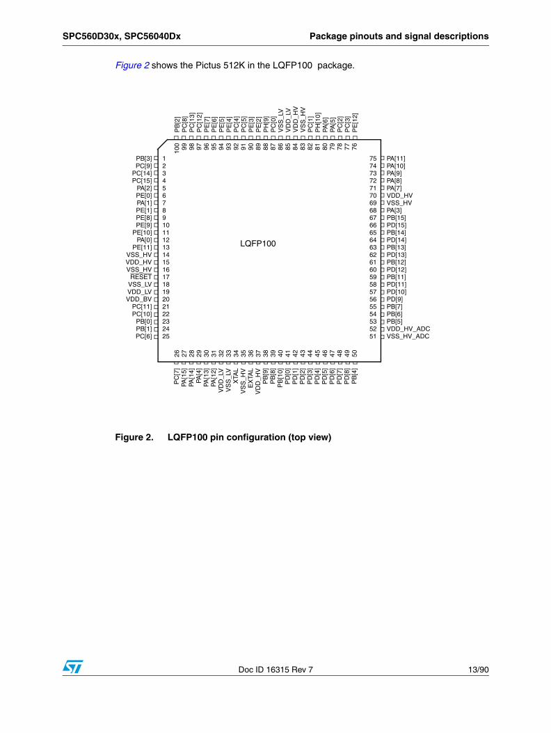
Figure 2 shows the Pictus 512K in the LQFP100 package.
Figure 2. LQFP100 pin configuration (top view)
12345678910111213141516171819202122232425
75747372717069686766656463626160595857565554535251
26 27 28 29 30 31 32 33 34 35 36 37 38 39 40 41 42 43 44 45 46 47 48 49 50
100 99 98 97 96 95 94 93 92 91 90 89 88 87 86 85 84 83 82 81 80 79 78 77 76
PB[3]PC[9]
PC[14]PC[15]
PA[2]PE[0]PA[1]PE[1]PE[8]PE[9]
PE[10]PA[0]
PE[11]VSS_HVVDD_HVVSS_HV
RESETVSS_LVVDD_LVVDD_BV
PC[11]PC[10]
PB[0]PB[1]PC[6]
PA[11]PA[10]PA[9]PA[8]PA[7]VDD_HVVSS_HVPA[3]PB[15]PD[15]PB[14]PD[14]PB[13]PD[13]PB[12]PD[12]PB[11]PD[11]PD[10]PD[9]PB[7]PB[6]PB[5]VDD_HV_ADCVSS_HV_ADC
PC
[7]
PA[1
5]PA
[14]
PA[4
]PA
[13]
PA[1
2]V
DD
_LV
VS
S_L
VX
TAL
VS
S_H
VE
XTA
LV
DD
_HV
PB
[9]
PB
[8]
PB
[10]
PD
[0]
PD
[1]
PD
[2]
PD
[3]
PD
[4]
PD
[5]
PD
[6]
PD
[7]
PD
[8]
PB
[4]
PB
[2]
PC
[8]
PC
[13]
PC
[12]
PE
[7]
PE
[6]
PE
[5]
PE
[4]
PC
[4]
PC
[5]
PE
[3]
PE
[2]
PH
[9]
PC
[0]
VS
S_L
VV
DD
_LV
VD
D_H
VV
SS
_HV
PC
[1]
PH
[10]
PA[6
]PA
[5]
PC
[2]
PC
[3]
PE
[12]
LQFP100
Package pinouts and signal descriptions SPC560D30x, SPC56040Dx
14/90 Doc ID 16315 Rev 7
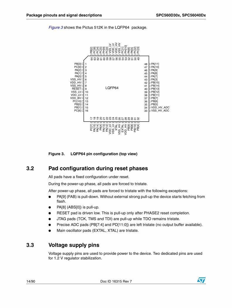
Figure 3 shows the Pictus 512K in the LQFP64 package.
Figure 3. LQFP64 pin configuration (top view)
3.2 Pad configuration during reset phasesAll pads have a fixed configuration under reset.
During the power-up phase, all pads are forced to tristate.
After power-up phase, all pads are forced to tristate with the following exceptions:
● PA[9] (FAB) is pull-down. Without external strong pull-up the device starts fetching from flash.
● PA[8] (ABS[0]) is pull-up.
● RESET pad is driven low. This is pull-up only after PHASE2 reset completion.
● JTAG pads (TCK, TMS and TDI) are pull-up while TDO remains tristate.
● Precise ADC pads (PB[7:4] and PD[11:0]) are left tristate (no output buffer available).
● Main oscillator pads (EXTAL, XTAL) are tristate.
3.3 Voltage supply pinsVoltage supply pins are used to provide power to the device. Two dedicated pins are used for 1.2 V regulator stabilization.
12345678910111213141516
48474645444342414039383736353433
17 18 19 20 21 22 23 24 25 26 27 28 29 30 31 32
64 63 62 61 60 59 58 57 56 55 54 53 52 51 50 49
PB[3]PC[9]PA[2]PA[1]PA[0]
VSS_HVVDD_HVVSS_HV
RESETVSS_LVVDD_LVVDD_BV
PC[10]PB[0]PB[1]PC[6]
PA[11] PA[10] PA[9] PA[8] PA[7] PA[3] PB[15] PB[14]PB[13]PB[12] PB[11] PB[7] PB[6] PB[5] VDD_HV_ADCVSS_HV_ADC
PC
[7]
PA[1
5]PA
[14]
PA[4
]PA
[13]
PA[1
2]V
DD
_LV
VS
S_L
VX
TAL
VS
S_H
VE
XTA
LV
DD
_HV
PB
[9]
PB
[8]
PB
[10]
PB
[4]
PB
[2]
PC
[8]
PC
[4]
PC
[5]
PH
[9]
PC
[0]
VS
S_L
VV
DD
_LV
VD
D_H
VV
SS
_HV
PC
[1]
PH
[10]
PA
[6]
PA[5
]P
C[2
] P
C[3
]
LQFP64

SPC560D30x, SPC56040Dx Package pinouts and signal descriptions
Doc ID 16315 Rev 7 15/90
3.4 Pad typesIn the device the following types of pads are available for system pins and functional port pins:
S = Slow(a)
M = Medium(a) (b)
F = Fast(a) (b)
I = Input only with analog feature(a)
J = Input/Output (‘S’ pad) with analog feature
X = Oscillator
3.5 System pinsThe system pins are listed in Table 5.
Table 4. Voltage supply pin descriptions
Port pin FunctionPin number
LQFP64 LQFP100
VDD_HV Digital supply voltage 7, 28, 34, 56 15, 37, 52, 70, 84
VSS_HV Digital ground 6, 8, 26, 33, 5514, 16, 35, 51, 69,
83
VDD_LV1.2V decoupling pins. Decoupling capacitor must be
connected between these pins and the nearest VSS_LV pin.(1)
11, 23, 57 19, 32, 85
VSS_LV1.2V decoupling pins. Decoupling capacitor must beconnected between these pins and the nearest VDD_LV pin.(1)
10, 24, 58 18, 33, 86
VDD_BV Internal regulator supply voltage 12 20
1. A decoupling capacitor must be placed between each of the three VDD_LV/VSS_LV supply pairs to ensure stable voltage (see the recommended operating conditions in the device datasheet for details).
a. See the I/O pad electrical characteristics in the device datasheet for details.
b. All medium and fast pads are in slow configuration by default at reset and can be configured as fast or medium (see the PCR[SRC] description in the device reference manual).
Table 5. System pin descriptions
Port pin FunctionI/O
directionPad type
RESET
configuration
Pin number
LQFP64 LQFP100
RESETBidirectional reset with Schmitt-Trigger characteristics and noise filter.
I/O MInput, weak pull-up only
after PHASE29 17

Package pinouts and signal descriptions SPC560D30x, SPC56040Dx
16/90 Doc ID 16315 Rev 7
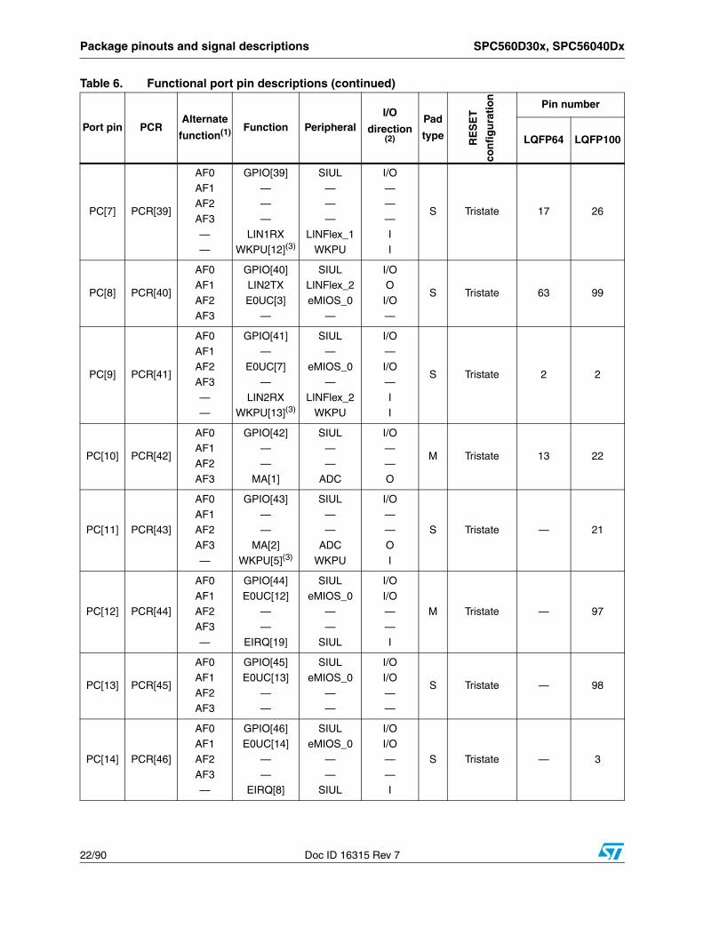
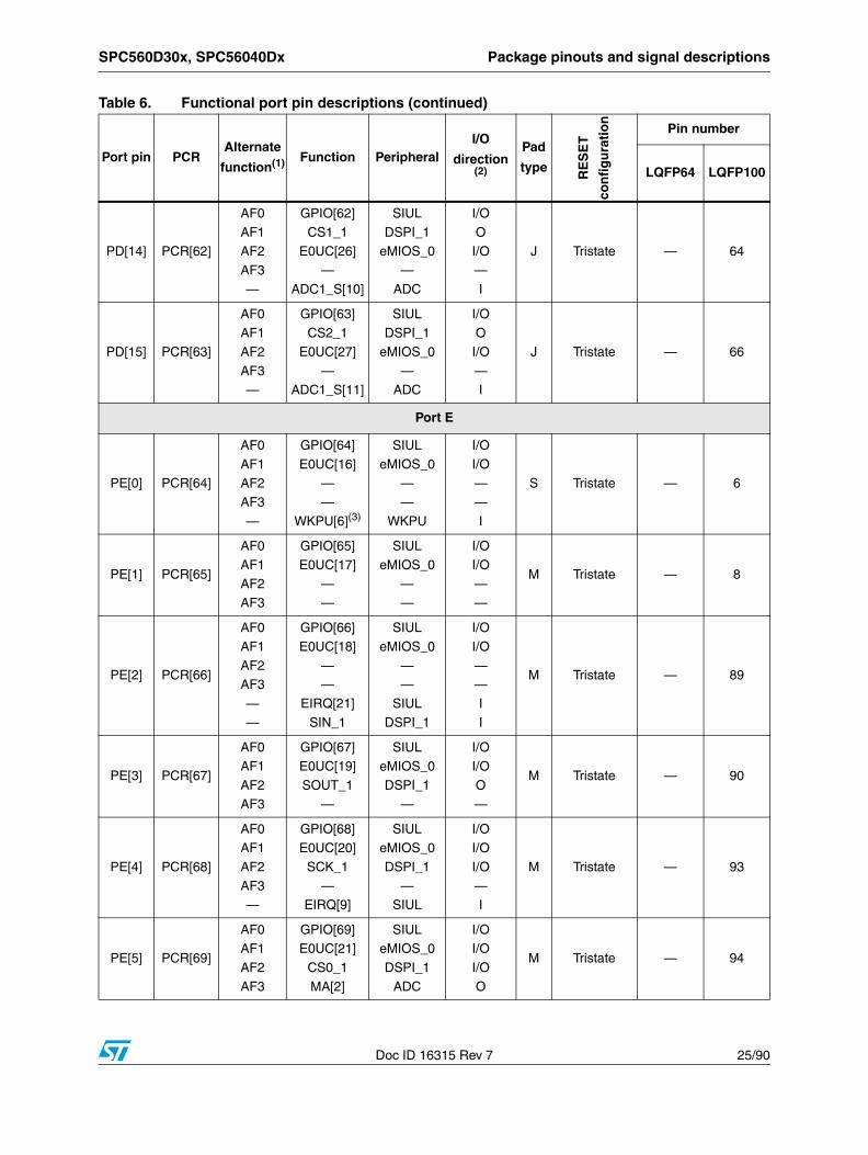
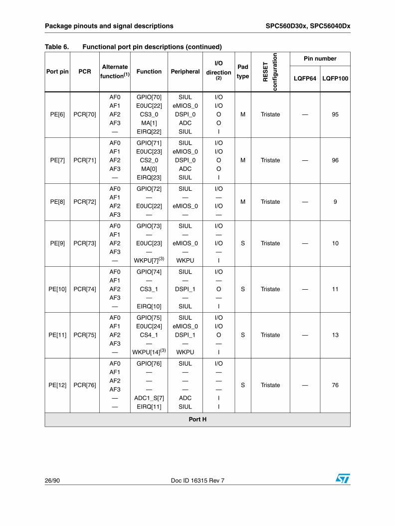
3.6 Functional portsThe functional port pins are listed in Table 6.
EXTAL
Analog output of the oscillator amplifier circuit, when the oscillator is not in bypass mode.Analog input for the clock generator when the oscillator is in bypass mode.(1)
I/O X Tristate 27 36
XTALAnalog input of the oscillator amplifier circuit. Needs to be grounded if oscillator is used in bypass mode.(1)
I X Tristate 25 34
1. Refer to the relevant section of the device datasheet.
Table 5. System pin descriptions (continued)
Port pin FunctionI/O
directionPad type
RESET
configuration
Pin number
LQFP64 LQFP100
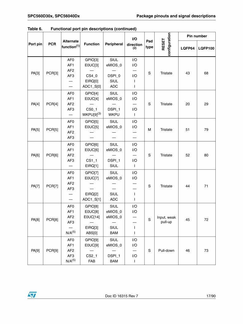
Table 6. Functional port pin descriptions
Port pin PCRAlternate
function(1) Function PeripheralI/O
direction(2)
Pad
type
RE
SE
T
con
fig
ura
tio
n
Pin number
LQFP64 LQFP100
Port A
PA[0] PCR[0]
AF0AF1
AF2
AF3—
GPIO[0]E0UC[0]
CLKOUT
E0UC[13]WKPU[19](3)
SIULeMIOS_0
CGL
eMIOS_0WKPU
I/OI/O
O
I/OI
M Tristate 5 12
PA[1] PCR[1]
AF0AF1
AF2
AF3—
—
GPIO[1]E0UC[1]
—
—NMI(4)
WKPU[2](3)
SIULeMIOS_0
—
—WKPU
WKPU
I/OI/O
—
—I
I
S Tristate 4 7
PA[2] PCR[2]
AF0
AF1
AF2AF3
—
GPIO[2]
E0UC[2]
—MA[2]
WKPU[3](3)
SIUL
eMIOS_0
—ADC
WKPU
I/O
I/O
—O
I
S Tristate 3 5
SPC560D30x, SPC56040Dx Package pinouts and signal descriptions
Doc ID 16315 Rev 7 17/90
PA[3] PCR[3]
AF0
AF1AF2
AF3
——
GPIO[3]
E0UC[3]—
CS4_0
EIRQ[0]ADC1_S[0]
SIUL
eMIOS_0—
DSPI_0
SIULADC
I/O
I/O—
I/O
II
S Tristate 43 68
PA[4] PCR[4]
AF0AF1
AF2
AF3—
GPIO[4]E0UC[4]
—
CS0_1WKPU[9](3)
SIULeMIOS_0
—
DSPI_1WKPU
I/OI/O
—
I/OI
S Tristate 20 29
PA[5] PCR[5]
AF0AF1
AF2
AF3
GPIO[5]E0UC[5]
—
—
SIULeMIOS_0
—
—
I/OI/O
—
—
M Tristate 51 79
PA[6] PCR[6]
AF0
AF1AF2
AF3
—
GPIO[6]
E0UC[6]—
CS1_1
EIRQ[1]
SIUL
eMIOS_0—
DSPI_1
SIUL
I/O
I/O—
I/O
I
S Tristate 52 80
PA[7] PCR[7]
AF0
AF1AF2
AF3
——
GPIO[7]
E0UC[7]—
—
EIRQ[2]ADC1_S[1]
SIUL
eMIOS_0—
—
SIULADC
I/O
I/O—
—
II
S Tristate 44 71
PA[8] PCR[8]
AF0AF1
AF2
AF3
—N/A(5)
GPIO[8]E0UC[8]
E0UC[14]
—
EIRQ[3]ABS[0]
SIULeMIOS_0
eMIOS_0
—
SIULBAM
I/OI/O
—
—
II
SInput, weak
pull-up45 72
PA[9] PCR[9]
AF0AF1
AF2
AF3N/A(5)
GPIO[9]E0UC[9]
—
CS2_1FAB
SIULeMIOS_0
—
DSPI_1BAM
I/OI/O
—
I/OI
S Pull-down 46 73
Table 6. Functional port pin descriptions (continued)
Port pin PCRAlternate
function(1) Function PeripheralI/O
direction(2)
Pad
type
RE
SE
T
con
fig
ura
tio
n
Pin number
LQFP64 LQFP100

Package pinouts and signal descriptions SPC560D30x, SPC56040Dx
18/90 Doc ID 16315 Rev 7
PA[10] PCR[10]
AF0
AF1AF2
AF3
—
GPIO[10]
E0UC[10]—
LIN2TX
ADC1_S[2]
SIUL
eMIOS_0—
LINFlex_2
ADC
I/O
I/O—
O
I
S Tristate 47 74
PA[11] PCR[11]
AF0
AF1AF2
AF3
——
—
GPIO[11]
E0UC[11]—
—
EIRQ[16]ADC1_S[3]
LIN2RX
SIUL
eMIOS_0—
—
SIULADC
LINFlex_2
I/O
I/O—
—
II
I
S Tristate 48 75
PA[12] PCR[12]
AF0
AF1
AF2AF3
—
—
GPIO[12]
—
——
EIRQ[17]
SIN_0
SIUL
—
——
SIUL
DSPI_0
I/O
—
——
I
I
S Tristate 22 31
PA[13] PCR[13]
AF0
AF1AF2
AF3
GPIO[13]
SOUT_0—
CS3_1
SIUL
DSPI_0—
DSPI_1
I/O
O—
I/O
M Tristate 21 30
PA[14] PCR[14]
AF0
AF1
AF2AF3
—
GPIO[14]
SCK_0
CS0_0E0UC[0]
EIRQ[4]
SIULDSPI_0
DSPI_0eMIOS_0
SIUL
I/O
I/O
I/OI/O
I
M Tristate 19 28
PA[15] PCR[15]
AF0
AF1
AF2
AF3—
GPIO[15]
CS0_0
SCK_0
E0UC[1]WKPU[10](3)
SIUL
DSPI_0
DSPI_0
eMIOS_0WKPU
I/O
I/O
I/O
I/OI
M Tristate 18 27
Port B
PB[0] PCR[16]
AF0AF1
AF2
AF3
GPIO[16]CAN0TX
—
LIN2TX
SIULFlexCAN_0
—
LINFlex_2
I/OO
—
O
M Tristate 14 23
Table 6. Functional port pin descriptions (continued)
Port pin PCRAlternate
function(1) Function PeripheralI/O
direction(2)
Pad
type
RE
SE
T
con
fig
ura
tio
n
Pin number
LQFP64 LQFP100

SPC560D30x, SPC56040Dx Package pinouts and signal descriptions
Doc ID 16315 Rev 7 19/90
PB[1] PCR[17]
AF0
AF1AF2
AF3
——
GPIO[17]
——
LIN0RX
WKPU[4](3)
CAN0RX
SIUL
——
LINFlex_0
WKPUFlexCAN_0
I/O
——
I
II
S Tristate 15 24
PB[2] PCR[18]
AF0AF1
AF2
AF3
GPIO[18]LIN0TX
—
—
SIULLINFlex_0
—
—
I/OO
—
—
M Tristate 64 100
PB[3] PCR[19]
AF0
AF1AF2
AF3
——
GPIO[19]
——
—
WKPU[11](3)
LIN0RX
SIUL
——
—
WKPULINFlex_0
I/O
——
—
II
S Tristate 1 1
PB[4] PCR[20]
AF0AF1
AF2
AF3—
GPIO[20]—
—
—ADC1_P[0]
SIUL—
—
—ADC
I—
—
—I
I Tristate 32 50
PB[5] PCR[21]
AF0AF1
AF2
AF3—
GPIO[21]—
—
—ADC1_P[1]
SIUL—
—
—ADC
I—
—
—I
I Tristate 35 53
PB[6] PCR[22]
AF0AF1
AF2
AF3
—
GPIO[22]—
—
—
ADC1_P[2]
SIUL—
—
—
ADC
I—
—
—
I
I Tristate 36 54
PB[7] PCR[23]
AF0
AF1AF2
AF3
—
GPIO[23]
——
—
ADC1_P[3]
SIUL
——
—
ADC
I
——
—
I
I Tristate 37 55
Table 6. Functional port pin descriptions (continued)
Port pin PCRAlternate
function(1) Function PeripheralI/O
direction(2)
Pad
type
RE
SE
T
con
fig
ura
tio
n
Pin number
LQFP64 LQFP100

Package pinouts and signal descriptions SPC560D30x, SPC56040Dx
20/90 Doc ID 16315 Rev 7
PB[8] PCR[24]
AF0
AF1AF2
AF3
——
GPIO[24]
——
—
ADC1_S[4]WKPU[25](3)
SIUL
——
—
ADCWKPU
I
——
—
II
I Tristate 30 39
PB[9] PCR[25]
AF0AF1
AF2
AF3—
—
GPIO[25]—
—
—ADC1_S[5]
WKPU[26](3)
SIUL—
—
—ADC
WKPU
I—
—
—I
I
I Tristate 29 38
PB[10] PCR[26]
AF0
AF1
AF2AF3
—
—
GPIO[26]
—
——
ADC1_S[6]
WKPU[8](3)
SIUL
—
——
ADC
WKPU
I/O
—
——
I
I
J Tristate 31 40
PB[11] PCR[27]
AF0
AF1AF2
AF3
—
GPIO[27]
E0UC[3]—
CS0_0
ADC1_S[12]
SIUL
eMIOS_0—
DSPI_0
ADC
I/O
I/O—
I/O
I
J Tristate 38 59
PB[12] PCR[28]
AF0
AF1AF2
AF3
—
GPIO[28]
E0UC[4]—
CS1_0
ADC1_X[0]
SIUL
eMIOS_0—
DSPI_0
ADC
I/O
I/O—
O
I
J Tristate 39 61
PB[13] PCR[29]
AF0
AF1
AF2AF3
—
GPIO[29]
E0UC[5]
—CS2_0
ADC1_X[1]
SIUL
eMIOS_0
—DSPI_0
ADC
I/O
I/O
—O
I
J Tristate 40 63
PB[14] PCR[30]
AF0
AF1
AF2AF3
—
GPIO[30]
E0UC[6]
—CS3_0
ADC1_X[2]
SIUL
eMIOS_0
—DSPI_0
ADC
I/O
I/O
—O
I
J Tristate 41 65
Table 6. Functional port pin descriptions (continued)
Port pin PCRAlternate
function(1) Function PeripheralI/O
direction(2)
Pad
type
RE
SE
T
con
fig
ura
tio
n
Pin number
LQFP64 LQFP100

SPC560D30x, SPC56040Dx Package pinouts and signal descriptions
Doc ID 16315 Rev 7 21/90
PB[15] PCR[31]
AF0
AF1AF2
AF3
—
GPIO[31]
E0UC[7]—
CS4_0
ADC1_X[3]
SIUL
eMIOS_0—
DSPI_0
ADC
I/O
I/O—
O
I
J Tristate 42 67
Port C
PC[0](6) PCR[32]
AF0
AF1AF2
AF3
GPIO[32]
—TDI
—
SIUL
—JTAGC
—
I/O
—I
—
MInput, weak
pull-up59 87
PC[1](6) PCR[33]
AF0
AF1
AF2AF3
GPIO[33]
—
TDO—
SIUL
—
JTAGC—
I/O
—
O—
F Tristate 54 82
PC[2] PCR[34]
AF0AF1
AF2
AF3—
GPIO[34]SCK_1
—
—EIRQ[5]
SIULDSPI_1
—
—SIUL
I/OI/O
—
—I
M Tristate 50 78
PC[3] PCR[35]
AF0AF1
AF2
AF3—
GPIO[35]CS0_1
MA[0]
—EIRQ[6]
SIULDSPI_1
ADC
—SIUL
I/OI/O
O
—I
S Tristate 49 77
PC[4] PCR[36]
AF0AF1
AF2
AF3
——
GPIO[36]—
—
—
SIN_1EIRQ[18]
SIUL—
—
—
DSPI_1SIUL
I/O—
—
—
II
M Tristate 62 92
PC[5] PCR[37]
AF0AF1
AF2
AF3—
GPIO[37]SOUT_1
—
—EIRQ[7]
SIULDSPI_1
—
—SIUL
I/OO
—
—I
M Tristate 61 91
PC[6] PCR[38]
AF0AF1
AF2
AF3
GPIO[38]LIN1TX
—
—
SIULLINFlex_1
—
—
I/OO
—
—
S Tristate 16 25
Table 6. Functional port pin descriptions (continued)
Port pin PCRAlternate
function(1) Function PeripheralI/O
direction(2)
Pad
type
RE
SE
T
con
fig
ura
tio
n
Pin number
LQFP64 LQFP100
Package pinouts and signal descriptions SPC560D30x, SPC56040Dx
22/90 Doc ID 16315 Rev 7
PC[7] PCR[39]
AF0
AF1AF2
AF3
——
GPIO[39]
——
—
LIN1RXWKPU[12](3)
SIUL
——
—
LINFlex_1WKPU
I/O
——
—
II
S Tristate 17 26
PC[8] PCR[40]
AF0AF1
AF2
AF3
GPIO[40]LIN2TX
E0UC[3]
—
SIULLINFlex_2
eMIOS_0
—
I/OO
I/O
—
S Tristate 63 99
PC[9] PCR[41]
AF0
AF1AF2
AF3
——
GPIO[41]
—E0UC[7]
—
LIN2RXWKPU[13](3)
SIUL
—eMIOS_0
—
LINFlex_2WKPU
I/O
—I/O
—
II
S Tristate 2 2
PC[10] PCR[42]
AF0AF1
AF2
AF3
GPIO[42]—
—
MA[1]
SIUL—
—
ADC
I/O—
—
O
M Tristate 13 22
PC[11] PCR[43]
AF0
AF1AF2
AF3
—
GPIO[43]
——
MA[2]
WKPU[5](3)
SIUL
——
ADC
WKPU
I/O
——
O
I
S Tristate — 21
PC[12] PCR[44]
AF0
AF1AF2
AF3
—
GPIO[44]
E0UC[12]—
—
EIRQ[19]
SIUL
eMIOS_0—
—
SIUL
I/O
I/O—
—
I
M Tristate — 97
PC[13] PCR[45]
AF0
AF1
AF2AF3
GPIO[45]
E0UC[13]
——
SIUL
eMIOS_0
——
I/O
I/O
——
S Tristate — 98
PC[14] PCR[46]
AF0AF1
AF2
AF3—
GPIO[46]E0UC[14]
—
—EIRQ[8]
SIULeMIOS_0
—
—SIUL
I/OI/O
—
—I
S Tristate — 3
Table 6. Functional port pin descriptions (continued)
Port pin PCRAlternate
function(1) Function PeripheralI/O
direction(2)
Pad
type
RE
SE
T
con
fig
ura
tio
n
Pin number
LQFP64 LQFP100

SPC560D30x, SPC56040Dx Package pinouts and signal descriptions
Doc ID 16315 Rev 7 23/90
PC[15] PCR[47]
AF0
AF1AF2
AF3
—
GPIO[47]
E0UC[15]—
—
EIRQ[20]
SIUL
eMIOS_0—
—
SIUL
I/O
I/O—
—
I
M Tristate — 4
Port D
PD[0] PCR[48]
AF0
AF1AF2
AF3
——
GPIO[48]
——
—
WKPU[27](3)
ADC1_P[4]
SIUL
——
—
WKPUADC
I
——
—
II
I Tristate — 41
PD[1] PCR[49]
AF0AF1
AF2
AF3—
—
GPIO[49]—
—
—WKPU[28](3)
ADC1_P[5]
SIUL—
—
—WKPU
ADC
I—
—
—I
I
I Tristate — 42
PD[2] PCR[50]
AF0
AF1
AF2AF3
—
GPIO[50]
—
——
ADC1_P[6]
SIUL
—
——
ADC
I
—
——
I
I Tristate — 43
PD[3] PCR[51]
AF0
AF1
AF2AF3
—
GPIO[51]
—
——
ADC1_P[7]
SIUL
—
——
ADC
I
—
——
I
I Tristate — 44
PD[4] PCR[52]
AF0AF1
AF2
AF3—
GPIO[52]—
—
—ADC1_P[8]
SIUL—
—
—ADC
I—
—
—I
I Tristate — 45
PD[5] PCR[53]
AF0AF1
AF2
AF3—
GPIO[53]—
—
—ADC1_P[9]
SIUL—
—
—ADC
I—
—
—I
I Tristate — 46
Table 6. Functional port pin descriptions (continued)
Port pin PCRAlternate
function(1) Function PeripheralI/O
direction(2)
Pad
type
RE
SE
T
con
fig
ura
tio
n
Pin number
LQFP64 LQFP100

Package pinouts and signal descriptions SPC560D30x, SPC56040Dx
24/90 Doc ID 16315 Rev 7
PD[6] PCR[54]
AF0
AF1AF2
AF3
—
GPIO[54]
——
—
ADC1_P[10]
SIUL
——
—
ADC
I
——
—
I
I Tristate — 47
PD[7] PCR[55]
AF0
AF1AF2
AF3
—
GPIO[55]
——
—
ADC1_P[11]
SIUL
——
—
ADC
I
——
—
I
I Tristate — 48
PD[8] PCR[56]
AF0
AF1AF2
AF3
—
GPIO[56]
——
—
ADC1_P[12]
SIUL
——
—
ADC
I
——
—
I
I Tristate — 49
PD[9] PCR[57]
AF0
AF1AF2
AF3
—
GPIO[57]
——
—
ADC1_P[13]
SIUL
——
—
ADC
I
——
—
I
I Tristate — 56
PD[10] PCR[58]
AF0
AF1AF2
AF3
—
GPIO[58]
——
—
ADC1_P[14]
SIUL
——
—
ADC
I
——
—
I
I Tristate — 57
PD[11] PCR[59]
AF0
AF1AF2
AF3
—
GPIO[59]
——
—
ADC1_P[15]
SIUL
——
—
ADC
I
——
—
I
I Tristate — 58
PD[12] PCR[60]
AF0
AF1
AF2AF3
—
GPIO[60]
CS5_0
E0UC[24]—
ADC1_S[8]
SIUL
DSPI_0
eMIOS_0—
ADC
I/O
O
I/O—
I
J Tristate — 60
PD[13] PCR[61]
AF0
AF1
AF2AF3
—
GPIO[61]
CS0_1
E0UC[25]—
ADC1_S[9]
SIUL
DSPI_1
eMIOS_0—
ADC
I/O
I/O
I/O—
I
J Tristate — 62
Table 6. Functional port pin descriptions (continued)
Port pin PCRAlternate
function(1) Function PeripheralI/O
direction(2)
Pad
type
RE
SE
T
con
fig
ura
tio
n
Pin number
LQFP64 LQFP100
SPC560D30x, SPC56040Dx Package pinouts and signal descriptions
Doc ID 16315 Rev 7 25/90
PD[14] PCR[62]
AF0
AF1AF2
AF3
—
GPIO[62]
CS1_1E0UC[26]
—
ADC1_S[10]
SIUL
DSPI_1eMIOS_0
—
ADC
I/O
OI/O
—
I
J Tristate — 64
PD[15] PCR[63]
AF0
AF1AF2
AF3
—
GPIO[63]
CS2_1E0UC[27]
—
ADC1_S[11]
SIUL
DSPI_1eMIOS_0
—
ADC
I/O
OI/O
—
I
J Tristate — 66
Port E
PE[0] PCR[64]
AF0
AF1AF2
AF3
—
GPIO[64]
E0UC[16]—
—
WKPU[6](3)
SIUL
eMIOS_0—
—
WKPU
I/O
I/O—
—
I
S Tristate — 6
PE[1] PCR[65]
AF0
AF1AF2
AF3
GPIO[65]
E0UC[17]—
—
SIUL
eMIOS_0—
—
I/O
I/O—
—
M Tristate — 8
PE[2] PCR[66]
AF0
AF1
AF2AF3
—
—
GPIO[66]
E0UC[18]
——
EIRQ[21]
SIN_1
SIUL
eMIOS_0
——
SIUL
DSPI_1
I/O
I/O
——
I
I
M Tristate — 89
PE[3] PCR[67]
AF0
AF1
AF2AF3
GPIO[67]
E0UC[19]
SOUT_1—
SIUL
eMIOS_0
DSPI_1—
I/O
I/O
O—
M Tristate — 90
PE[4] PCR[68]
AF0AF1
AF2
AF3—
GPIO[68]E0UC[20]
SCK_1
—EIRQ[9]
SIULeMIOS_0
DSPI_1
—SIUL
I/OI/O
I/O
—I
M Tristate — 93
PE[5] PCR[69]
AF0AF1
AF2
AF3
GPIO[69]E0UC[21]
CS0_1
MA[2]
SIULeMIOS_0
DSPI_1ADC
I/OI/O
I/O
O
M Tristate — 94
Table 6. Functional port pin descriptions (continued)
Port pin PCRAlternate
function(1) Function PeripheralI/O
direction(2)
Pad
type
RE
SE
T
con
fig
ura
tio
n
Pin number
LQFP64 LQFP100
Package pinouts and signal descriptions SPC560D30x, SPC56040Dx
26/90 Doc ID 16315 Rev 7
PE[6] PCR[70]
AF0
AF1AF2
AF3
—
GPIO[70]
E0UC[22]CS3_0
MA[1]
EIRQ[22]
SIUL
eMIOS_0DSPI_0
ADC
SIUL
I/O
I/OO
O
I
M Tristate — 95
PE[7] PCR[71]
AF0
AF1AF2
AF3
—
GPIO[71]
E0UC[23]CS2_0
MA[0]
EIRQ[23]
SIUL
eMIOS_0DSPI_0
ADC
SIUL
I/O
I/OO
O
I
M Tristate — 96
PE[8] PCR[72]
AF0
AF1AF2
AF3
GPIO[72]
—E0UC[22]
—
SIUL
—eMIOS_0
—
I/O
—I/O
—
M Tristate — 9
PE[9] PCR[73]
AF0
AF1
AF2AF3
—
GPIO[73]
—
E0UC[23]—
WKPU[7](3)
SIUL
—
eMIOS_0—
WKPU
I/O
—
I/O—
I
S Tristate — 10
PE[10] PCR[74]
AF0
AF1
AF2AF3
—
GPIO[74]
—
CS3_1—
EIRQ[10]
SIUL
—
DSPI_1—
SIUL
I/O
—
O—
I
S Tristate — 11
PE[11] PCR[75]
AF0
AF1
AF2AF3
—
GPIO[75]
E0UC[24]
CS4_1—
WKPU[14](3)
SIUL
eMIOS_0
DSPI_1—
WKPU
I/O
I/O
O—
I
S Tristate — 13
PE[12] PCR[76]
AF0AF1
AF2
AF3—
—
GPIO[76]—
—
—ADC1_S[7]
EIRQ[11]
SIUL—
—
—ADC
SIUL
I/O—
—
—I
I
S Tristate — 76
Port H
Table 6. Functional port pin descriptions (continued)
Port pin PCRAlternate
function(1) Function PeripheralI/O
direction(2)
Pad
type
RE
SE
T
con
fig
ura
tio
n
Pin number
LQFP64 LQFP100

SPC560D30x, SPC56040Dx Package pinouts and signal descriptions
Doc ID 16315 Rev 7 27/90
PH[9](6) PCR[121]
AF0
AF1AF2
AF3
GPIO[121]
—TCK
—
SIUL
—JTAGC
—
I/O
—I
—
SInput, weak
pull-up60 88
PH[10](6) PCR[122]
AF0
AF1
AF2AF3
GPIO[122]
—
TMS—
SIUL
—
JTAGC—
I/O
—
I—
SInput, weak
pull-up53 81
1. Alternate functions are chosen by setting the values of the PCR.PA bitfields inside the SIUL module. PCR.PA = 00 AF0; PCR.PA = 01 AF1; PCR.PA = 10 AF2; PCR.PA = 11 AF3. This is intended to select the output functions; to use one of the input functions, the PCR.IBE bit must be written to ‘1’, regardless of the values selected in the PCR.PA bitfields. For this reason, the value corresponding to an input only function is reported as “—”.
2. Multiple inputs are routed to all respective modules internally. The input of some modules must be configured by setting the values of the PSMIO.PADSELx bitfields inside the SIUL module.
3. All WKPU pins also support external interrupt capability. See “wakeup unit” chapter of the device reference manual for further details.
4. NMI has higher priority than alternate function. When NMI is selected, the PCR.AF field is ignored.
5. “Not applicable” because these functions are available only while the device is booting. Refer to “BAM” chapter of the device reference manual for details.
6. Out of reset all the functional pins except PC[0:1] and PH[9:10] are available to the user as GPIO.PC[0:1] are available as JTAG pins (TDI and TDO respectively).PH[9:10] are available as JTAG pins (TCK and TMS respectively).If the user configures these JTAG pins in GPIO mode the device is no longer compliant with IEEE 1149.1 2001.
Table 6. Functional port pin descriptions (continued)
Port pin PCRAlternate
function(1) Function PeripheralI/O
direction(2)
Pad
type
RE
SE
T
con
fig
ura
tio
n
Pin number
LQFP64 LQFP100
Electrical characteristics SPC560D30x, SPC56040Dx
28/90 Doc ID 16315 Rev 7
4 Electrical characteristics
4.1 IntroductionThis section contains electrical characteristics of the device as well as temperature and power considerations.
This product contains devices to protect the inputs against damage due to high static voltages. However, it is advisable to take precautions to avoid application of any voltage higher than the specified maximum rated voltages.
To enhance reliability, unused inputs can be driven to an appropriate logic voltage level (VDD or VSS). This can be done by the internal pull-up or pull-down, which is provided by the product for most general purpose pins.
The parameters listed in the following tables represent the characteristics of the device and its demands on the system.
In the tables where the device logic provides signals with their respective timing characteristics, the symbol “CC” for Controller Characteristics is included in the Symbol column.
In the tables where the external system must provide signals with their respective timing characteristics to the device, the symbol “SR” for System Requirement is included in the Symbol column.
4.2 Parameter classificationThe electrical parameters shown in this supplement are guaranteed by various methods. To give the customer a better understanding, the classifications listed in Table 7 are used and the parameters are tagged accordingly in the tables where appropriate.
Note: The classification is shown in the column labeled “C” in the parameter tables where appropriate.
Table 7. Parameter classifications
Classification tag Tag description
P Those parameters are guaranteed during production testing on each individual device.
CThose parameters are achieved by the design characterization by measuring a statistically relevant sample size across process variations.
TThose parameters are achieved by design characterization on a small sample size from typical devices under typical conditions unless otherwise noted. All values shown in the typical column are within this category.
D Those parameters are derived mainly from simulations.

SPC560D30x, SPC56040Dx Electrical characteristics
Doc ID 16315 Rev 7 29/90
4.3 NVUSRO registerBit values in the Non-Volatile User Options (NVUSRO) Register control portions of the device configuration, namely electrical parameters such as high voltage supply and oscillator margin, as well as digital functionality (watchdog enable/disable after reset).
For a detailed description of the NVUSRO register, please refer to the device reference manual.
4.3.1 NVUSRO[PAD3V5V] field description
The DC electrical characteristics are dependent on the PAD3V5V bit value. Table 8 shows how NVUSRO[PAD3V5V] controls the device configuration.
4.3.2 NVUSRO[OSCILLATOR_MARGIN] field description
The fast external crystal oscillator consumption is dependent on the OSCILLATOR_MARGIN bit value. Table 9 shows how NVUSRO[OSCILLATOR_MARGIN] controls the device configuration.
4.3.3 NVUSRO[WATCHDOG_EN] field description
The watchdog enable/disable configuration after reset is dependent on the WATCHDOG_EN bit value. Table 9 shows how NVUSRO[WATCHDOG_EN] controls the device configuration.
Table 8. PAD3V5V field description
Value(1)
1. Default manufacturing value is ‘1’. Value can be programmed by customer in Shadow Flash.
Description
0 High voltage supply is 5.0 V
1 High voltage supply is 3.3 V
Table 9. OSCILLATOR_MARGIN field description
Value(1)
1. Default manufacturing value is ‘1’. Value can be programmed by customer in Shadow Flash.
Description
0 Low consumption configuration (4 MHz/8 MHz)
1 High margin configuration (4 MHz/16 MHz)
Table 10. WATCHDOG_EN field description
Value(1)
1. Default manufacturing value is ‘1’. Value can be programmed by customer in Shadow Flash.
Description
0 Disable after reset
1 Enable after reset

Electrical characteristics SPC560D30x, SPC56040Dx
30/90 Doc ID 16315 Rev 7
4.4 Absolute maximum ratings
Note: Stresses exceeding the recommended absolute maximum ratings may cause permanent damage to the device. This is a stress rating only and functional operation of the device at these or any other conditions above those indicated in the operational sections of this specification are not implied. Exposure to absolute maximum rating conditions for extended periods may affect device reliability. During overload conditions (VIN > VDD or VIN < VSS), the voltage on pins with respect to ground (VSS) must not exceed the recommended values.
Table 11. Absolute maximum ratings
Symbol Parameter ConditionsValue
UnitMin Max
VSS SR Digital ground on VSS_HV pins — 0 0 V
VDD SRVoltage on VDD_HV pins with respect to ground (VSS)
— 0.3 6.0 V
VSS_LV SRVoltage on VSS_LV (low voltage digital supply) pins with respect to ground (VSS)
— VSS 0.1 VSS + 0.1 V
VDD_BV SRVoltage on VDD_BV (regulator supply) pin with respect to ground (VSS)
— 0.3 6.0V
Relative to VDD VDD 0.3 VDD + 0.3
VSS_ADC SRVoltage on VSS_HV_ADC (ADC reference) pin with respect to ground (VSS)
— VSS 0.1 VSS + 0.1 V
VDD_ADC SRVoltage on VDD_HV_ADC (ADC reference) pin with respect to ground (VSS)
— 0.3 6.0V
Relative to VDD VDD 0.3 VDD + 0.3
VIN SRVoltage on any GPIO pin with respect to ground (VSS)
— 0.3 6.0V
Relative to VDD VDD 0.3 VDD + 0.3
IINJPAD SRInjected input current on any pin during overload condition
— 10 10 mA
IINJSUM SRAbsolute sum of all injected input currents during overload condition
— 50 50 mA
IAVGSEG SRSum of all the static I/O current within a supply segment(1)
VDD = 5.0 V ± 10%, PAD3V5V = 0
— 70
mAVDD = 3.3 V ± 10%, PAD3V5V = 1
— 64
ICORELV SRLow voltage static current sink through VDD_BV
— — 150 mA
TSTORAGE SR Storage temperature — 55 150 °C
1. Supply segments are described in Section 4.7.5, I/O pad current specification.

SPC560D30x, SPC56040Dx Electrical characteristics
Doc ID 16315 Rev 7 31/90
4.5 Recommended operating conditions
Table 12. Recommended operating conditions (3.3 V)
Symbol C Parameter ConditionsValue
UnitMin Max
VSS SR — Digital ground on VSS_HV pins — 0 0 V
VDD(1) SR —
Voltage on VDD_HV pins with respect to ground (VSS)
— 3.0 3.6 V
VSS_LV(2) SR —
Voltage on VSS_LV (low voltage digital supply) pins with respect to ground (VSS)
— VSS 0.1 VSS + 0.1 V
VDD_BV(3) SR —
Voltage on VDD_BV pin (regulator supply) with respect to ground (VSS)
— 3.0 3.6V
Relative to VDD VDD 0.1 VDD + 0.1
VSS_ADC SR —Voltage on VSS_HV_ADC (ADC reference) pin with respect to ground (VSS)
— VSS 0.1 VSS + 0.1 V
VDD_ADC(4) SR —
Voltage on VDD_HV_ADC pin (ADC reference) with respect to ground (VSS)
— 3.0(5) 3.6V
Relative to VDD VDD 0.1 VDD + 0.1
VIN SR —Voltage on any GPIO pin with respect to ground (VSS)
— VSS 0.1 —V
Relative to VDD — VDD + 0.1
IINJPAD SR —Injected input current on any pin during overload condition
— 5 5 mA
IINJSUM SR —Absolute sum of all injected input currents during overload condition
— 50 50 mA
TVDD SR — VDD slope to ensure correct power up(6) — 3.0(7)250 x 103
(0.25 [V/µs])
V/s
1. 100 nF capacitance needs to be provided between each VDD/VSS pair.
2. 330 nF capacitance needs to be provided between each VDD_LV/VSS_LV supply pair.
3. 470 nF capacitance needs to be provided between VDD_BV and the nearest VSS_LV (higher value may be needed depending on external regulator characteristics).
4. 100 nF capacitance needs to be provided between VDD_ADC/VSS_ADC pair.
5. Full electrical specification cannot be guaranteed when voltage drops below 3.0 V. In particular, ADC electrical characteristics and I/Os DC electrical specification may not be guaranteed. When voltage drops below VLVDHVL, device is reset.
6. Guaranteed by device validation
7. Minimum value of TVDD must be guaranteed until VDD reaches 2.6 V (maximum value of VPORH)
Table 13. Recommended operating conditions (5.0 V)
Symbol C Parameter ConditionsValue
UnitMin Max
VSS SR — Digital ground on VSS_HV pins — 0 0 V
VDD(1) SR —
Voltage on VDD_HV pins with respect to ground (VSS)
— 4.5 5.5V
Voltage drop(2) 3.0 5.5

Electrical characteristics SPC560D30x, SPC56040Dx
32/90 Doc ID 16315 Rev 7
Note: SRAM data retention is guaranteed with VDD_LV not below 1.08 V.
VSS_LV(3) SR —
Voltage on VSS_LV (low voltage digital supply) pins with respect to ground (VSS)
— VSS 0.1 VSS + 0.1 V
VDD_BV(4) SR —
Voltage on VDD_BV pin (regulator supply) with respect to ground (VSS)
— 4.5 5.5
VVoltage drop(2) 3.0 5.5
Relative to VDD VDD 0.1 VDD + 0.1
VSS_ADC SR —Voltage on VSS_HV_ADC (ADC reference) pin with respect to ground (VSS
— VSS 0.1 VSS + 0.1 V
VDD_ADC(5) SR —
Voltage on VDD_HV_ADC pin (ADC reference) with respect to ground (VSS)
— 4.5 5.5
VVoltage drop(2) 3.0 5.5
Relative to VDD VDD 0.1 VDD + 0.1
VIN SR —Voltage on any GPIO pin with respect to ground (VSS)
— VSS 0.1 —V
Relative to VDD — VDD + 0.1
IINJPAD SR —Injected input current on any pin during overload condition
— 5 5 mA
IINJSUM SR —Absolute sum of all injected input currents during overload condition
— 50 50 mA
TVDD SR — VDD slope to ensure correct power up(6) — 3.0(7)250 x 103
(0.25 [V/µs])
V/s
1. 100 nF capacitance needs to be provided between each VDD/VSS pair.
2. Full device operation is guaranteed by design when the voltage drops below 4.5 V down to 3.6 V. However, certain analog electrical characteristics will not be guaranteed to stay within the stated limits.
3. 330 nF capacitance needs to be provided between each VDD_LV/VSS_LV supply pair.
4. 470 nF capacitance needs to be provided between VDD_BV and the nearest VSS_LV (higher value may be needed depending on external regulator characteristics).
5. 100 nF capacitance needs to be provided between VDD_ADC/VSS_ADC pair.
6. Guaranteed by device validation
7. Minimum value of TVDD must be guaranteed until VDD reaches 2.6 V (maximum value of VPORH)
Table 13. Recommended operating conditions (5.0 V) (continued)
Symbol C Parameter ConditionsValue
UnitMin Max

SPC560D30x, SPC56040Dx Electrical characteristics
Doc ID 16315 Rev 7 33/90
4.6 Thermal characteristics
4.6.1 Package thermal characteristics
4.6.2 Power considerations
The average chip-junction temperature, TJ, in degrees Celsius, may be calculated using Equation 1:
Table 14. LQFP thermal characteristics(1)
Symbol C Parameter Conditions(2) Value Unit
RJA CC DThermal resistance, junction-to-ambient natural convection(3)
Single-layer board —1sLQFP64 72.1
°C/WLQFP100 65.2
Four-layer board — 2s2pLQFP64 57.3
LQFP100 51.8
RJB CC D Thermal resistance, junction-to-board(4) Four-layer board — 2s2pLQFP64 44.1
°C/WLQFP100 41.3
RJC CC D Thermal resistance, junction-to-case(5)
Single-layer board — 1sLQFP64 26.5
°C/WLQFP100 23.9
Four-layer board — 2s2pLQFP64 26.2
LQFP100 23.7
JB CC DJunction-to-board thermal characterization parameter, natural convection
Single-layer board — 1sLQFP64 41
°C/WLQFP100 41.6
Four-layer board — 2s2pLQFP64 43
LQFP100 43.4
JC CC DJunction-to-case thermal characterization parameter, natural convection
Single-layer board — 1sLQFP64 11.5
°C/WLQFP100 10.4
Four-layer board — 2s2pLQFP64 11.1
LQFP100 10.2
1. Thermal characteristics are targets based on simulation that are subject to change per device characterization.
2. VDD = 3.3 V ± 10% / 5.0 V ± 10%, TA = –40 to 125 °C
3. Junction-to-ambient thermal resistance determined per JEDEC JESD51-3 and JESD51-7. Thermal test board meets JEDEC specification for this package. When Greek letters are not available, the symbols are typed as RthJA.
4. Junction-to-board thermal resistance determined per JEDEC JESD51-8. Thermal test board meets JEDEC specification for the specified package. When Greek letters are not available, the symbols are typed as RthJB.
5. Junction-to-case at the top of the package determined using MIL-STD 883 Method 1012.1. The cold plate temperature is used for the case temperature. Reported value includes the thermal resistance of the interface layer. When Greek letters are not available, the symbols are typed as RthJC.

Electrical characteristics SPC560D30x, SPC56040Dx
34/90 Doc ID 16315 Rev 7
Equation 1 TJ = TA + (PD x RJA)
Where:
TA is the ambient temperature in °C.
RJA is the package junction-to-ambient thermal resistance, in °C/W.
PD is the sum of PINT and PI/O (PD = PINT + PI/O).
PINT is the product of IDD and VDD, expressed in watts. This is the chip internal power.
PI/O represents the power dissipation on input and output pins; user determined.
Most of the time for the applications, PI/O< PINT and may be neglected. On the other hand, PI/O may be significant, if the device is configured to continuously drive external modules and/or memories.
An approximate relationship between PD and TJ (if PI/O is neglected) is given by:
Equation 2 PD = K / (TJ + 273 °C)
Therefore, solving equations 1 and 2:
Equation 3 K = PD x (TA + 273 °C) + RJA x PD2
Where:
K is a constant for the particular part, which may be determined from Equation 3 by measuring PD (at equilibrium) for a known TA. Using this value of K, the values of PD and TJ may be obtained by solving equations 1 and 2 iteratively for any value of TA.
4.7 I/O pad electrical characteristics
4.7.1 I/O pad types
The device provides four main I/O pad types depending on the associated alternate functions:
● Slow pads—These pads are the most common pads, providing a good compromise between transition time and low electromagnetic emission.
● Medium pads—These pads provide transition fast enough for the serial communication channels with controlled current to reduce electromagnetic emission.
● Input only pads—These pads are associated to ADC channels (ADC_P[X]) providing low input leakage.
Medium pads can use slow configuration to reduce electromagnetic emission except for PC[1], that is medium only, at the cost of reducing AC performance.
4.7.2 I/O input DC characteristics
Table 15 provides input DC electrical characteristics as described in Figure 4.

SPC560D30x, SPC56040Dx Electrical characteristics
Doc ID 16315 Rev 7 35/90
Figure 4. Input DC electrical characteristics definition
VIL
VIN
VIH
PDIx = ‘1’
VDD
VHYS
(GPDI register of SIUL)
PDIx = ‘0’
Table 15. I/O input DC electrical characteristics
Symbol C Parameter Conditions(1)Value
UnitMin Typ Max
VIH SR PInput high level CMOS (Schmitt Trigger)
— 0.65VDD — VDD+0.4 V
VIL SR PInput low level CMOS (Schmitt Trigger)
— 0.4 — 0.35VDD V
VHYS CC CInput hysteresis CMOS (Schmitt Trigger)
— 0.1VDD — — V
ILKG CC
D
Digital input leakageNo injection on adjacent pin
TA = 40 °C — 2 200
nA
D TA = 25 °C — 2 200
D TA = 85 °C — 5 300
D TA = 105 °C — 12 500
P TA = 125 °C — 70 1000
WFI(2) SR P Digital input filtered pulse — — — 40 ns
WNFI(2) SR P Digital input not filtered pulse — 1000 — — ns
1. VDD = 3.3 V ± 10% / 5.0 V ± 10%, TA = 40 to 125 °C, unless otherwise specified
2. In the range from 40 to 1000 ns, pulses can be filtered or not filtered, according to operating temperature and voltage.

Electrical characteristics SPC560D30x, SPC56040Dx
36/90 Doc ID 16315 Rev 7
4.7.3 I/O output DC characteristics
The following tables provide DC characteristics for bidirectional pads:
● Table 16 provides weak pull figures. Both pull-up and pull-down resistances are supported.
● Table 17 provides output driver characteristics for I/O pads when in SLOW configuration.
● Table 18 provides output driver characteristics for I/O pads when in MEDIUM configuration.
Table 16. I/O pull-up/pull-down DC electrical characteristics
Symbol C Parameter Conditions(1)Value
UnitMin Typ Max
|IWPU| CC
PWeak pull-up current absolute value
VIN = VIL, VDD = 5.0 V ± 10%PAD3V5V = 0 10 — 150
µAC PAD3V5V = 1(2) 10 — 250
P VIN = VIL, VDD = 3.3 V ± 10% PAD3V5V = 1 10 — 150
|IWPD| CC
PWeak pull-down current absolute value
VIN = VIH, VDD = 5.0 V ± 10%PAD3V5V = 0 10 — 150
µAC PAD3V5V = 1(2) 10 — 250
P VIN = VIH, VDD = 3.3 V ± 10% PAD3V5V = 1 10 — 150
1. VDD = 3.3 V ± 10% / 5.0 V ± 10%, TA = 40 to 125 °C, unless otherwise specified.
2. The configuration PAD3V5 = 1 when VDD = 5 V is only a transient configuration during power-up. All pads but RESET are configured in input or in high impedance state.
Table 17. SLOW configuration output buffer electrical characteristics
Symbol C Parameter Conditions(1)Value
UnitMin Typ Max
VOH CC
P
Output high levelSLOW configuration
Push Pull
IOH = 2 mA,VDD = 5.0 V ± 10%, PAD3V5V = 0(recommended)
0.8VDD — —
VCIOH = 2 mA,VDD = 5.0 V ± 10%, PAD3V5V = 1(2) 0.8VDD — —
CIOH = 1 mA,VDD = 3.3 V ± 10%, PAD3V5V = 1(recommended)
VDD 0.8 — —
VOL CC
P
Output low levelSLOW configuration
Push Pull
IOL = 2 mA,VDD = 5.0 V ± 10%, PAD3V5V = 0(recommended)
— — 0.1VDD
VCIOL = 2 mA,VDD = 5.0 V ± 10%, PAD3V5V = 1(2) — — 0.1VDD
CIOL = 1 mA,VDD = 3.3 V ± 10%, PAD3V5V = 1(recommended)
— — 0.5
1. VDD = 3.3 V ± 10% / 5.0 V ± 10%, TA = 40 to 125 °C, unless otherwise specified

SPC560D30x, SPC56040Dx Electrical characteristics
Doc ID 16315 Rev 7 37/90
2. The configuration PAD3V5 = 1 when VDD = 5 V is only a transient configuration during power-up. All pads but RESET are configured in input or in high impedance state.
Table 18. MEDIUM configuration output buffer electrical characteristics
Symbol C Parameter Conditions(1)Value
UnitMin Typ Max
VOH CC
C
Output high level
MEDIUM configurationPush Pull
IOH = 3.8 mA,VDD = 5.0 V ± 10%, PAD3V5V = 0
0.8VDD — —
V
PIOH = 2 mA,VDD = 5.0 V ± 10%, PAD3V5V = 0(recommended)
0.8VDD — —
CIOH = 1 mA,
VDD = 5.0 V ± 10%, PAD3V5V = 1(2) 0.8VDD — —
CIOH = 1 mA,
VDD = 3.3 V ± 10%, PAD3V5V = 1 (recommended)
VDD 0.8 — —
CIOH = 100 µA,VDD = 5.0 V ± 10%, PAD3V5V = 0
0.8VDD — —
VOL CC
C
Output low level
MEDIUM configurationPush Pull
IOL = 3.8 mA,VDD = 5.0 V ± 10%, PAD3V5V = 0
— — 0.2VDD
V
PIOL = 2 mA,VDD = 5.0 V ± 10%, PAD3V5V = 0(recommended)
— — 0.1VDD
CIOL = 1 mA,
VDD = 5.0 V ± 10%, PAD3V5V = 1(2) — — 0.1VDD
CIOL = 1 mA,
VDD = 3.3 V ± 10%, PAD3V5V = 1 (recommended)
— — 0.5
CIOL = 100 µA,
VDD = 5.0 V ± 10%, PAD3V5V = 0— — 0.1VDD
1. VDD = 3.3 V ± 10% / 5.0 V ± 10%, TA = 40 to 125 °C, unless otherwise specified
2. The configuration PAD3V5 = 1 when VDD = 5 V is only a transient configuration during power-up. All pads but RESET are configured in input or in high impedance state.

Electrical characteristics SPC560D30x, SPC56040Dx
38/90 Doc ID 16315 Rev 7
4.7.4 Output pin transition times
4.7.5 I/O pad current specification
The I/O pads are distributed across the I/O supply segment. Each I/O supply segment is associated to a VDD/VSS supply pair as described in Table 20.
Table 21 provides I/O consumption figures.
In order to ensure device reliability, the average current of the I/O on a single segment should remain below the IAVGSEG maximum value.
Table 19. Output pin transition times
Symbol C Parameter Conditions(1)Value
UnitMin Typ Max
ttr CC
D
Output transition time output pin(2)
SLOW configuration
CL = 25 pF
VDD = 5.0 V ± 10%, PAD3V5V = 0
— — 50
ns
T CL = 50 pF — — 100
D CL = 100 pF — — 125
D CL = 25 pF
VDD = 3.3 V ± 10%, PAD3V5V = 1
— — 50
T CL = 50 pF — — 100
D CL = 100 pF — — 125
ttr CC
D
Output transition time output pin(2)
MEDIUM configuration
CL = 25 pFVDD = 5.0 V ± 10%, PAD3V5V = 0
SIUL.PCRx.SRC = 1
— — 10
ns
T CL = 50 pF — — 20
D CL = 100 pF — — 40
D CL = 25 pFVDD = 3.3 V ± 10%, PAD3V5V = 1
SIUL.PCRx.SRC = 1
— — 12
T CL = 50 pF — — 25
D CL = 100 pF — — 40
1. VDD = 3.3 V ± 10% / 5.0 V ± 10%, TA = 40 to 125 °C, unless otherwise specified
2. CL includes device and package capacitances (CPKG < 5 pF).
Table 20. I/O supply segment
PackageSupply segment
1 2 3 4
LQFP100 pin 16 – pin 35 pin 37 – pin 69 pin 70 – pin 83 pin 84 – pin 15
LQFP64 pin 8 – pin 26 pin 28 – pin 55 pin 56 – pin 7 —

SPC560D30x, SPC56040Dx Electrical characteristics
Doc ID 16315 Rev 7 39/90
Table 22 provides the weight of concurrent switching I/Os.
In order to ensure device functionality, the sum of the weight of concurrent switching I/Os on a single segment should remain below 100%.
Table 21. I/O consumption
Symbol C Parameter Conditions(1)Value
UnitMin Typ Max
ISWTSLW(2) CC D
Dynamic I/O current for SLOW configuration
CL = 25 pF
VDD = 5.0 V ± 10%,PAD3V5V = 0
— — 20
mAVDD = 3.3 V ± 10%,PAD3V5V = 1
— — 16
ISWTMED(2) CC D
Dynamic I/O current for MEDIUM configuration
CL = 25 pF
VDD = 5.0 V ± 10%,PAD3V5V = 0
— — 29
mAVDD = 3.3 V ± 10%,PAD3V5V = 1
— — 17
IRMSSLW CC DRoot mean square I/O current for SLOW configuration
CL = 25 pF, 2 MHzVDD = 5.0 V ± 10%,PAD3V5V = 0
— — 2.3
mA
CL = 25 pF, 4 MHz — — 3.2
CL = 100 pF, 2 MHz — — 6.6
CL = 25 pF, 2 MHzVDD = 3.3 V ± 10%,PAD3V5V = 1
— — 1.6
CL = 25 pF, 4 MHz — — 2.3
CL = 100 pF, 2 MHz — — 4.7
IRMSMED CC D
Root mean square I/O current for MEDIUM configuration
CL = 25 pF, 13 MHzVDD = 5.0 V ± 10%, PAD3V5V = 0
— — 6.6
mA
CL = 25 pF, 40 MHz — — 13.4
CL = 100 pF, 13 MHz — — 18.3
CL = 25 pF, 13 MHzVDD = 3.3 V ± 10%, PAD3V5V = 1
— — 5
CL = 25 pF, 40 MHz — — 8.5
CL = 100 pF, 13 MHz — — 11
IAVGSEG SR DSum of all the static I/O current within a supply segment
VDD = 5.0 V ± 10%, PAD3V5V = 0 — — 70mA
VDD = 3.3 V ± 10%, PAD3V5V = 1 — — 65
1. VDD = 3.3 V ± 10% / 5.0 V ± 10%, TA = 40 to 125 °C, unless otherwise specified
2. Stated maximum values represent peak consumption that lasts only a few ns during I/O transition.
Table 22. I/O weight(1)
Pad
LQFP100/LQFP64
Weight 5 V Weight 3.3 V
SRC(2) = 0 SRC = 1 SRC = 0 SRC = 1
PB[3] 9% 9% 10% 10%
PC[9] 8% 8% 10% 10%

Electrical characteristics SPC560D30x, SPC56040Dx
40/90 Doc ID 16315 Rev 7
PC[14] 8% 8% 10% 10%
PC[15] 8% 11% 9% 10%
PA[2] 8% 8% 9% 9%
PE[0] 7% 7% 9% 9%
PA[1] 7% 7% 8% 8%
PE[1] 7% 10% 8% 8%
PE[8] 6% 9% 8% 8%
PE[9] 6% 6% 7% 7%
PE[10] 6% 6% 7% 7%
PA[0] 5% 7% 6% 7%
PE[11] 5% 5% 6% 6%
PC[11] 7% 7% 9% 9%
PC[10] 8% 11% 9% 10%
PB[0] 8% 11% 9% 10%
PB[1] 8% 8% 10% 10%
PC[6] 8% 8% 10% 10%
PC[7] 8% 8% 10% 10%
PA[15] 8% 11% 9% 10%
PA[14] 7% 11% 9% 9%
PA[4] 7% 7% 8% 8%
PA[13] 7% 10% 8% 9%
PA[12] 7% 7% 8% 8%
PB[9] 1% 1% 1% 1%
PB[8] 1% 1% 1% 1%
PB[10] 5% 5% 6% 6%
PD[0] 1% 1% 1% 1%
PD[1] 1% 1% 1% 1%
PD[2] 1% 1% 1% 1%
PD[3] 1% 1% 1% 1%
PD[4] 1% 1% 1% 1%
PD[5] 1% 1% 1% 1%
PD[6] 1% 1% 1% 1%
Table 22. I/O weight(1) (continued)
Pad
LQFP100/LQFP64
Weight 5 V Weight 3.3 V
SRC(2) = 0 SRC = 1 SRC = 0 SRC = 1

SPC560D30x, SPC56040Dx Electrical characteristics
Doc ID 16315 Rev 7 41/90
PD[7] 1% 1% 1% 1%
PD[8] 1% 1% 1% 1%
PB[4] 1% 1% 1% 1%
PB[5] 1% 1% 1% 1%
PB[6] 1% 1% 1% 1%
PB[7] 1% 1% 1% 1%
PD[9] 1% 1% 1% 1%
PD[10] 1% 1% 1% 1%
PD[11] 1% 1% 1% 1%
PB[11] 9% 9% 11% 11%
PD[12] 8% 8% 10% 10%
PB[12] 8% 8% 10% 10%
PD[13] 8% 8% 9% 9%
PB[13] 8% 8% 9% 9%
PD[14] 7% 7% 9% 9%
PB[14] 7% 7% 8% 8%
PD[15] 7% 7% 8% 8%
PB[15] 6% 6% 7% 7%
PA[3] 6% 6% 7% 7%
PA[7] 4% 4% 5% 5%
PA[8] 4% 4% 5% 5%
PA[9] 4% 4% 5% 5%
PA[10] 5% 5% 6% 6%
PA[11] 5% 5% 6% 6%
PE[12] 5% 5% 6% 6%
PC[3] 5% 5% 6% 6%
PC[2] 5% 7% 6% 6%
PA[5] 5% 6% 5% 6%
PA[6] 4% 4% 5% 5%
PC[1] 5% 17% 4% 12%
PC[0] 6% 9% 7% 8%
PE[2] 7% 10% 8% 9%
Table 22. I/O weight(1) (continued)
Pad
LQFP100/LQFP64
Weight 5 V Weight 3.3 V
SRC(2) = 0 SRC = 1 SRC = 0 SRC = 1
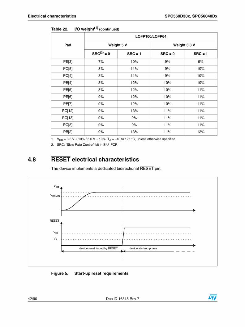
Electrical characteristics SPC560D30x, SPC56040Dx
42/90 Doc ID 16315 Rev 7
4.8 RESET electrical characteristicsThe device implements a dedicated bidirectional RESET pin.
Figure 5. Start-up reset requirements
PE[3] 7% 10% 9% 9%
PC[5] 8% 11% 9% 10%
PC[4] 8% 11% 9% 10%
PE[4] 8% 12% 10% 10%
PE[5] 8% 12% 10% 11%
PE[6] 9% 12% 10% 11%
PE[7] 9% 12% 10% 11%
PC[12] 9% 13% 11% 11%
PC[13] 9% 9% 11% 11%
PC[8] 9% 9% 11% 11%
PB[2] 9% 13% 11% 12%
1. VDD = 3.3 V ± 10% / 5.0 V ± 10%, TA = 40 to 125 °C, unless otherwise specified
2. SRC: “Slew Rate Control” bit in SIU_PCR
Table 22. I/O weight(1) (continued)
Pad
LQFP100/LQFP64
Weight 5 V Weight 3.3 V
SRC(2) = 0 SRC = 1 SRC = 0 SRC = 1
VIL
VDD
device reset forced by RESET
VDDMIN
RESET
VIH
device start-up phase

SPC560D30x, SPC56040Dx Electrical characteristics
Doc ID 16315 Rev 7 43/90
Figure 6. Noise filtering on reset signal
VRESET
VIL
VIH
VDD
filtered by hysteresis
filtered by lowpass filter
WFRST
WNFRST
hw_rst
‘1’
‘0’filtered by lowpass filter
WFRST
unknown resetstate device under hardware reset
Table 23. Reset electrical characteristics
Symbol C Parameter Conditions(1)Value
UnitMin Typ Max
VIH SR PInput High Level CMOS (Schmitt Trigger)
— 0.65VDD — VDD + 0.4 V
VIL SR PInput low Level CMOS (Schmitt Trigger)
— 0.4 — 0.35VDD V
VHYS CC CInput hysteresis CMOS (Schmitt Trigger)
— 0.1VDD — — V
VOL CC P Output low level
Push Pull, IOL = 2 mA,VDD = 5.0 V ± 10%, PAD3V5V = 0(recommended)
— — 0.1VDD
VPush Pull, IOL = 1 mA,VDD = 5.0 V ± 10%, PAD3V5V = 1(2) — — 0.1VDD
Push Pull, IOL = 1 mA,VDD = 3.3 V ± 10%, PAD3V5V = 1 (recommended)
— — 0.5

Electrical characteristics SPC560D30x, SPC56040Dx
44/90 Doc ID 16315 Rev 7
4.9 Power management electrical characteristics
4.9.1 Voltage regulator electrical characteristics
The device implements an internal voltage regulator to generate the low voltage core supply VDD_LV from the high voltage ballast supply VDD_BV. The regulator itself is supplied by the common I/O supply VDD. The following supplies are involved:
● HV: High voltage external power supply for voltage regulator module. This must be provided externally through VDD power pin.
● BV: High voltage external power supply for internal ballast module. This must be provided externally through VDD_BV power pin. Voltage values should be aligned with VDD.
● LV: Low voltage internal power supply for core, FMPLL and flash digital logic. This is generated by the internal voltage regulator but provided outside to connect stability
ttr CC DOutput transition time output pin(3)
MEDIUM configuration
CL = 25 pF,VDD = 5.0 V ± 10%, PAD3V5V = 0
— — 10
ns
CL = 50 pF,VDD = 5.0 V ± 10%, PAD3V5V = 0
— — 20
CL = 100 pF,VDD = 5.0 V ± 10%, PAD3V5V = 0
— — 40
CL = 25 pF,VDD = 3.3 V ± 10%, PAD3V5V = 1
— — 12
CL = 50 pF,VDD = 3.3 V ± 10%, PAD3V5V = 1
— — 25
CL = 100 pF,VDD = 3.3 V ± 10%, PAD3V5V = 1
— — 40
WFRST SR PRESET input filtered pulse
— — — 40 ns
WNFRST SR PRESET input not filtered pulse
— 1000 — — ns
|IWPU| CC PWeak pull-up current absolute value
VDD = 3.3 V ± 10%, PAD3V5V = 1 10 — 150
µAVDD = 5.0 V ± 10%, PAD3V5V = 0 10 — 150
VDD = 5.0 V ± 10%, PAD3V5V = 1(4) 10 — 250
1. VDD = 3.3 V ± 10% / 5.0 V ± 10%, TA = 40 to 125 °C, unless otherwise specified
2. This is a transient configuration during power-up, up to the end of reset PHASE2 (refer to RGM module section of the device reference manual).
3. CL includes device and package capacitance (CPKG < 5 pF).
4. The configuration PAD3V5 = 1 when VDD = 5 V is only transient configuration during power-up. All pads but RESET are configured in input or in high impedance state.
Table 23. Reset electrical characteristics (continued)
Symbol C Parameter Conditions(1)Value
UnitMin Typ Max

SPC560D30x, SPC56040Dx Electrical characteristics
Doc ID 16315 Rev 7 45/90
capacitor. It is further split into four main domains to ensure noise isolation between critical LV modules within the device:
– LV_COR: Low voltage supply for the core. It is also used to provide supply for FMPLL through double bonding.
– LV_CFLA: Low voltage supply for code flash module. It is supplied with dedicated ballast and shorted to LV_COR through double bonding.
– LV_DFLA: Low voltage supply for data flash module. It is supplied with dedicated ballast and shorted to LV_COR through double bonding.
– LV_PLL: Low voltage supply for FMPLL. It is shorted to LV_COR through double bonding.
Figure 7. Voltage regulator capacitance connection
The internal voltage regulator requires external capacitance (CREGn) to be connected to the device in order to provide a stable low voltage digital supply to the device. Capacitances should be placed on the board as near as possible to the associated pins. Care should also be taken to limit the serial inductance of the board to less than 5 nH.
Each decoupling capacitor must be placed between each of the three VDD_LV/VSS_LV supply pairs to ensure stable voltage (see Section 4.5, Recommended operating conditions).
CR
EG
1 (L
V_C
OR
/LV
_DF
LA)
DEVICE
VSS_LV
VDD_BV
VDD_LV
CD
EC
1 (B
alla
st d
ecou
plin
g)
VSS_LV VDD_LV VDD
VSS_LV VDD_LV
CREG2 (LV_COR/LV_CFLA)
CREG3 CDEC2
DEVICE
VDD_BV
I
VDD_LVn
VREF
VDD
Voltage Regulator
VSSVSS_LVn
(supply/IO decoupling)(LV_COR/LV_PLL)

Electrical characteristics SPC560D30x, SPC56040Dx
46/90 Doc ID 16315 Rev 7
Table 24. Voltage regulator electrical characteristics
Symbol C Parameter Conditions(1)Value
UnitMin Typ Max
CREGn SR —Internal voltage regulator external capacitance
— 200 — 500 nF
RREG SR —Stability capacitor equivalent serial resistance
Range:
10 kHz to 20 MHz— — 0.2
CDEC1 SR — Decoupling capacitance(2) ballast
VDD_BV/VSS_LV pair:
VDD_BV = 4.5 V to 5.5 V100(3)
470(4)
—
nFVDD_BV/VSS_LV pair:
VDD_BV = 3 V to 3.6 V400 —
CDEC2 SR —Decoupling capacitance regulator supply
VDD/VSS pair 10 100 — nF
VMREG CCT
Main regulator output voltageBefore exiting from reset — 1.32 —
VP After trimming 1.16 1.28 —
IMREG SR —Main regulator current provided to VDD_LV domain
— — — 150 mA
IMREGINT CC DMain regulator module current consumption
IMREG = 200 mA — — 2mA
IMREG = 0 mA — — 1
VLPREG CC P Low-power regulator output voltage After trimming 1.16 1.28 — V
ILPREG SR —Low power regulator current provided to VDD_LV domain
— — — 15 mA
ILPREGINT CC
DLow-power regulator module current consumption
ILPREG = 15 mA;TA = 55 °C
— — 600
µA
—ILPREG = 0 mA;TA = 55 °C
— 5 —
VULPREG CC PUltra low power regulator output voltage
After trimming 1.16 1.28 — V
IULPREG SR —Ultra low power regulator current provided to VDD_LV domain
— — — 5 mA
IULPREGINT CC DUltra low power regulator module current consumption
IULPREG = 5 mA;TA = 55 °C
— — 100
µAIULPREG = 0 mA;TA = 55 °C
— 2 —
IDD_BV CC DIn-rush average current on VDD_BV during power-up(5) — — — 300(6) mA
1. VDD = 3.3 V ± 10% / 5.0 V ± 10%, TA = 40 to 125 °C, unless otherwise specified.
2. This capacitance value is driven by the constraints of the external voltage regulator supplying the VDD_BV voltage. A typical value is in the range of 470 nF.
3. This value is acceptable to guarantee operation from 4.5 V to 5.5 V.
4. External regulator and capacitance circuitry must be capable of providing IDD_BV while maintaining supply VDD_BV in operating range.
5. In-rush average current is seen only for short time during power-up and on standby exit (maximum 20 µs, depending on external capacitances to be loaded).
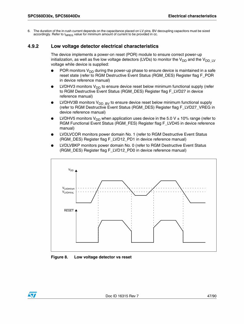
SPC560D30x, SPC56040Dx Electrical characteristics
Doc ID 16315 Rev 7 47/90
4.9.2 Low voltage detector electrical characteristics
The device implements a power-on reset (POR) module to ensure correct power-up initialization, as well as five low voltage detectors (LVDs) to monitor the VDD and the VDD_LV voltage while device is supplied:
● POR monitors VDD during the power-up phase to ensure device is maintained in a safe reset state (refer to RGM Destructive Event Status (RGM_DES) Register flag F_POR in device reference manual)
● LVDHV3 monitors VDD to ensure device reset below minimum functional supply (refer to RGM Destructive Event Status (RGM_DES) Register flag F_LVD27 in device reference manual)
● LVDHV3B monitors VDD_BV to ensure device reset below minimum functional supply (refer to RGM Destructive Event Status (RGM_DES) Register flag F_LVD27_VREG in device reference manual)
● LVDHV5 monitors VDD when application uses device in the 5.0 V ± 10% range (refer to RGM Functional Event Status (RGM_FES) Register flag F_LVD45 in device reference manual)
● LVDLVCOR monitors power domain No. 1 (refer to RGM Destructive Event Status (RGM_DES) Register flag F_LVD12_PD1 in device reference manual)
● LVDLVBKP monitors power domain No. 0 (refer to RGM Destructive Event Status (RGM_DES) Register flag F_LVD12_PD0 in device reference manual)
Figure 8. Low voltage detector vs reset
6. The duration of the in-rush current depends on the capacitance placed on LV pins. BV decoupling capacitors must be sized accordingly. Refer to IMREG value for minimum amount of current to be provided in cc.
VDD
VLVDHVxH
RESET
VLVDHVxL

Electrical characteristics SPC560D30x, SPC56040Dx
48/90 Doc ID 16315 Rev 7
4.10 Power consumptionTable 26 provides DC electrical characteristics for significant application modes. These values are indicative values; actual consumption depends on the application.
Table 25. Low voltage detector electrical characteristics
Symbol C Parameter Conditions(1)Value
UnitMin Typ Max
VPORUP SR P Supply for functional POR module
TA = 25 °C,after trimming
1.0 — 5.5 V
VPORH CC P Power-on reset threshold 1.5 — 2.6 V
VLVDHV3H CC T LVDHV3 low voltage detector high threshold — — 2.95 V
VLVDHV3L CC P LVDHV3 low voltage detector low threshold 2.6 — 2.9 V
VLVDHV3BH CC P LVDHV3B low voltage detector high threshold — — 2.95 V
VLVDHV3BL CC P LVDHV3B low voltage detector low threshold 2.6 — 2.9 V
VLVDHV5H CC T LVDHV5 low voltage detector high threshold — — 4.5 V
VLVDHV5L CC P LVDHV5 low voltage detector low threshold 3.8 — 4.4 V
VLVDLVCORL CC P LVDLVCOR low voltage detector low threshold 1.08 — 1.16 V
VLVDLVBKPL CC P LVDLVBKP low voltage detector low threshold 1.08 — 1.16 V
1. VDD = 3.3 V ± 10% / 5.0 V ± 10%, TA = 40 to 125 °C, unless otherwise specified
Table 26. Power consumption on VDD_BV and VDD_HV
Symbol C Parameter Conditions(1)Value
UnitMin Typ Max
IDDMAX(2) CC D
RUN mode maximum average current
— — 90 130(3) mA
IDDRUN(4) CC
T
RUN mode typical average current(5)
fCPU = 8 MHz — 7 —
mAT fCPU = 16 MHz — 18 —
T fCPU = 32 MHz — 29 —
P fCPU = 48 MHz — 40 100
IDDHALT CCC
HALT mode current(6) Slow internal RC oscillator (128 kHz) running
TA = 25 °C — 8 15mA
P TA = 125 °C — 14 25
IDDSTOP CC
P
STOP mode current(7) Slow internal RC oscillator (128 kHz) running
TA = 25 °C — 180 700(8)
µAD TA = 55 °C — 500 —
D TA = 85 °C — 1 6(8)
mAD TA = 105 °C — 2 9(8)
P TA = 125 °C — 4.5 12(8)

SPC560D30x, SPC56040Dx Electrical characteristics
Doc ID 16315 Rev 7 49/90
4.11 Flash memory electrical characteristicsThe data flash operation depends strongly on the code flash operation. If code flash is switched-off, the data flash is disabled.
4.11.1 Program/Erase characteristics
Table 27 shows the program and erase characteristics.
IDDSTDBY CC
P
STANDBY mode current(9) Slow internal RC oscillator (128 kHz) running
TA = 25 °C — 30 100
µA
D TA = 55 °C — 75 —
D TA = 85 °C — 180 700
D TA = 105 °C — 315 1000
P TA = 125 °C — 560 1700
1. VDD = 3.3 V ± 10% / 5.0 V ± 10%, TA = 40 to 125 °C, unless otherwise specified
2. Running consumption does not include I/Os toggling which is highly dependent on the application. The given value is thought to be a worst case value with all peripherals running, and code fetched from code flash while modify operation ongoing on data flash. Notice that this value can be significantly reduced by application: switch off not used peripherals (default), reduce peripheral frequency through internal prescaler, fetch from RAM most used functions, use low power mode when possible.
3. Higher current may be sinked by device during power-up and standby exit. Please refer to in-rush average current on Table 24.
4. RUN current measured with typical application with accesses on both flash memory and SRAM.
5. Only for the “P” classification: Code fetched from SRAM: serial IPs CAN and LIN in loop-back mode, DSPI as Master, PLL as system clock (3 × Multiplier) peripherals on (eMIOS/CTU/ADC) and running at maximum frequency, periodic SW/WDG timer reset enabled.
6. Data flash power down. Code flash in low power. SIRC (128 kHz) and FIRC (16 MHz) on. 10 MHz XTAL clock. FlexCAN: 0 ON (clocked but no reception or transmission). LINFlex: instances: 0, 1, 2 ON (clocked but no reception or transmission), instance: 3 clocks gated. eMIOS: instance: 0 ON (16 channels on PA[0]–PA[11] and PC[12]–PC[15]) with PWM 20 kHz, instance: 1 clock gated. DSPI: instance: 0 (clocked but no communication). RTC/API ON.PIT ON. STM ON. ADC ON but no conversion except 2 analog watchdogs.
7. Only for the “P” classification: No clock, FIRC (16 MHz) off, SIRC (128 kHz) on, PLL off, HPVreg off, ULPVreg/LPVreg on. All possible peripherals off and clock gated. Flash in power down mode.
8. When going from RUN to STOP mode and the core consumption is > 6 mA, it is normal operation for the main regulator module to be kept on by the on-chip current monitoring circuit. This is most likely to occur with junction temperatures exceeding 125 °C and under these circumstances, it is possible for the current to initially exceed the maximum STOP specification by up to 2 mA. After entering stop, the application junction temperature will reduce to the ambient level and the main regulator will be automatically switched off when the load current is below 6 mA.
9. Only for the “P” classification: ULPVreg on, HP/LPVreg off, 16 KB SRAM on, device configured for minimum consumption, all possible modules switched off.
Table 26. Power consumption on VDD_BV and VDD_HV (continued)
Symbol C Parameter Conditions(1)Value
UnitMin Typ Max
Table 27. Program and erase specifications (code flash)
Symbol C Parameter
Value
UnitMin Typ(1) Initial
max(2) Max(3)
tdwprogram CC C Double word (64 bits) program time(4) — 22 50 500 µs
t16Kpperase CC C 16 KB block preprogram and erase time — 300 500 5000 ms

Electrical characteristics SPC560D30x, SPC56040Dx
50/90 Doc ID 16315 Rev 7
t32Kpperase CC C 32 KB block preprogram and erase time — 400 600 5000 ms
t128Kpperase CC C 128 KB block preprogram and erase time — 800 1300 7500 ms
tesus CC C Erase suspend latency — — 30 30 µs
1. Typical program and erase times assume nominal supply values and operation at 25 °C. All times are subject to change pending device characterization.
2. Initial factory condition: < 100 program/erase cycles, 25 °C, typical supply voltage.
3. The maximum program and erase times occur after the specified number of program/erase cycles. These maximum values are characterized but not guaranteed.
4. Actual hardware programming times. This does not include software overhead.
Table 27. Program and erase specifications (code flash)
Symbol C Parameter
Value
UnitMin Typ(1) Initial
max(2) Max(3)
Table 28. Program and erase specifications (data flash)
Symbol C Parameter
Value
UnitMin Typ(1) Initial
max(2) Max(3)
tswprogram CC C Single word (32 bits) program time(4) — 30 70 300 µs
t16Kpperase CC C 16 KB block preprogram and erase time — 700 800 1500 ms
tBank_D CC C 64 KB block preprogram and erase time — 1900 2300 4800 ms
1. Typical program and erase times assume nominal supply values and operation at 25 °C. All times are subject to change pending device characterization.
2. Initial factory condition: < 100 program/erase cycles, 25 °C, typical supply voltage.
3. The maximum program and erase times occur after the specified number of program/erase cycles. These maximum values are characterized but not guaranteed.
4. Actual hardware programming times. This does not include software overhead.
Table 29. Flash module life
Symbol C Parameter ConditionsValue
UnitMin Typ Max
P/E CC C
Number of program/erase cycles per block over the operating temperature range (TJ)
16 KB blocks 100000 — — cycles
32 KB blocks 10000 100000 — cycles
128 KB blocks 1000 100000 — cycles
Retention CC CMinimum data retention at 85 °C average ambient temperature(1)
Blocks with0–1000 P/E cycles
20 — —
yearsBlocks with1001–10000 P/E cycles
10 — —
Blocks with10001–100000 P/E cycles
5 — —
1. Ambient temperature averaged over application duration. It is recommended not to exceed the product operating temperature range.

SPC560D30x, SPC56040Dx Electrical characteristics
Doc ID 16315 Rev 7 51/90
ECC circuitry provides correction of single bit faults and is used to improve further automotive reliability results. Some units will experience single bit corrections throughout the life of the product with no impact to product reliability.
4.11.2 Flash power supply DC characteristics
Table 31 shows the power supply DC characteristics on external supply.
Note: Power supply for data flash is actually provided by code flash; this means that data flash cannot work if code flash is not powered.
4.11.3 Start-up/Switch-off timings
Table 30. Flash memory read access timing
Symbol C ParameterConditions
(1) Max Unit
fCFREAD CCP Maximum working frequency for reading code flash memory at given
number of wait states in worst conditions
2 wait states 48MHz
C 0 wait states 20
fDFREAD CC PMaximum working frequency for reading data flash memory at given
number of wait states in worst conditions6 wait states 48 MHz
1. VDD = 3.3 V ± 10% / 5.0 V ± 10%, TA = 40 to 125 °C, unless otherwise specified
Table 31. Flash power supply DC electrical characteristics
Symbol C Parameter Conditions(1)Value
UnitMin Typ Max
ICFREAD CC D Sum of the current consumption onVDDHV and VDDBV on read access
Flash module read
fCPU = 48 MHz
Code flash — — 33 mA
IDFREAD CC D Data flash — — 4 mA
ICFMOD CC D Sum of the current consumption onVDDHV and VDDBV on matrixmodification (program/erase)
Program/Erase on-going
while reading flash registers,
fCPU = 48 MHz
Code flash — — 33 mA
IDFMOD CC D Data flash — — 6 mA
IFLPW CC DSum of the current consumption onVDDHV and VDDBV duringflash low-power mode
— Code flash — — 910 µA
ICFPWD CC D Sum of the current consumption onVDDHV and VDDBV duringflash power-down mode
—Code flash — — 125 µA
IDFPWD CC D Data flash — — 25 µA
1. VDD = 3.3 V ± 10% / 5.0 V ± 10%, TA = 40 to 125 °C, unless otherwise specified
Table 32. Start-up time/Switch-off time
Symbol C Parameter Conditions(1)Value
UnitMin Typ Max
tFLARSTEXITCC
T Delay for flash module to exit reset modeCode flash — — 125 µs
Data flash — — 150 µs

Electrical characteristics SPC560D30x, SPC56040Dx
52/90 Doc ID 16315 Rev 7
4.12 Electromagnetic compatibility (EMC) characteristicsSusceptibility tests are performed on a sample basis during product characterization.
4.12.1 Designing hardened software to avoid noise problems
EMC characterization and optimization are performed at component level with a typical application environment and simplified MCU software. It should be noted that good EMC performance is highly dependent on the user application and the software in particular.
Therefore it is recommended that the user apply EMC software optimization and prequalification tests in relation with the EMC level requested for his application.
● Software recommendations The software flowchart must include the management of runaway conditions such as:
– Corrupted program counter
– Unexpected reset
– Critical data corruption (control registers...)
● Prequalification trials Most of the common failures (unexpected reset and program counter corruption) can be reproduced by manually forcing a low state on the reset pin or the oscillator pins for 1 second.
To complete these trials, ESD stress can be applied directly on the device. When unexpected behavior is detected, the software can be hardened to prevent unrecoverable errors occurring (see the application note Software Techniques For Improving Microcontroller EMC Performance (AN1015)).
4.12.2 Electromagnetic interference (EMI)
The product is monitored in terms of emission based on a typical application. This emission test conforms to the IEC 61967-1 standard, which specifies the general conditions for EMI measurements.
tFLALPEXITCC
TDelay for flash module to exit low-power mode(2) Code flash — — 0.5 µs
tFLAPDEXITCC
TDelay for flash module to exit power-down mode
Code flash — — 30 µs
Data flash — — 30(3) µs
tFLALPENTRYCC
TDelay for flash module to enter low-power mode
Code flash — — 0.5 µs
tFLAPDENTRYCC
TDelay for flash module to enter power-down mode
Code flash — — 1.5 µs
Data flash — — 4(3) µs
1. VDD = 3.3 V ± 10% / 5.0 V ± 10%, TA = 40 to 125 °C, unless otherwise specified
2. Data flash does not support low-power mode
3. If code flash is already switched-on.
Table 32. Start-up time/Switch-off time (continued)
Symbol C Parameter Conditions(1)Value
UnitMin Typ Max

SPC560D30x, SPC56040Dx Electrical characteristics
Doc ID 16315 Rev 7 53/90
4.12.3 Absolute maximum ratings (electrical sensitivity)
Based on two different tests (ESD and LU) using specific measurement methods, the product is stressed in order to determine its performance in terms of electrical sensitivity.
Electrostatic discharge (ESD)
Electrostatic discharges (a positive then a negative pulse separated by 1 second) are applied to the pins of each sample according to each pin combination. The sample size depends on the number of supply pins in the device (3 parts × (n + 1) supply pin). This test conforms to the AEC-Q100-002/-003/-011 standard. For more details, refer to the application note Electrostatic Discharge Sensitivity Measurement (AN1181).
Table 33. EMI radiated emission measurement(1)(2)
Symbol C Parameter ConditionsValue
UnitMin Typ Max
— SR — Scan range — 0.150 — 1000 MHz
fCPU SR — Operating frequency — — 48 — MHz
VDD_LV SR — LV operating voltages — — 1.28 — V
SEMI CC T Peak level
VDD = 5 V, TA = 25 °C,LQFP100 packageTest conforming to IEC 61967-2,fOSC = 8 MHz/fCPU = 48 MHz
No PLL frequency modulation
— — 18 dBµV
± 2% PLL frequencymodulation
— — 14 dBµV
1. EMI testing and I/O port waveforms per IEC 61967-1, -2, -4
2. For information on conducted emission and susceptibility measurement (norm IEC 61967-4), please contact your local marketing representative.
Table 34. ESD absolute maximum ratings(1) (2)
Symbol C Ratings Conditions Class Max value
Unit
VESD(HBM)CC
TElectrostatic discharge voltage(Human Body Model)
TA = 25 °Cconforming to AEC-Q100-002
H1C 2000 V
VESD(MM)CC
TElectrostatic discharge voltage(Machine Model)
TA = 25 °Cconforming to AEC-Q100-003
M2 200 V
VESD(CDM)CC
TElectrostatic discharge voltage(Charged Device Model)
TA = 25 °Cconforming to AEC-Q100-011
C3A500 V
750 (corners) V
1. All ESD testing is in conformity with CDF-AEC-Q100 Stress Test Qualification for Automotive Grade Integrated Circuits.
2. A device will be defined as a failure if after exposure to ESD pulses the device no longer meets the device specification requirements. Complete DC parametric and functional testing shall be performed per applicable device specification at room temperature followed by hot temperature, unless specified otherwise in the device specification.

Electrical characteristics SPC560D30x, SPC56040Dx
54/90 Doc ID 16315 Rev 7
Static latch-up (LU)
Two complementary static tests are required on six parts to assess the latch-up performance:
● A supply overvoltage is applied to each power supply pin.
● A current injection is applied to each input, output and configurable I/O pin.
These tests are compliant with the EIA/JESD 78 IC latch-up standard.
Table 35. Latch-up results
Symbol C Parameter Conditions Class
LU CC T Static latch-up classTA = 125 °Cconforming to JESD 78
II level A

SPC560D30x, SPC56040Dx Electrical characteristics
Doc ID 16315 Rev 7 55/90
4.13 Fast external crystal oscillator (4 to 16 MHz) electrical characteristicsThe device provides an oscillator/resonator driver. Figure 9 describes a simple model of the internal oscillator driver and provides an example of a connection for an oscillator or a resonator.
Table 36 provides the parameter description of 4 MHz to 16 MHz crystals used for the design simulations.
Figure 9. Crystal oscillator and resonator connection scheme
C2
C1
Cry
stal
XTAL
EXTAL
Res
onat
or
XTAL
EXTAL
DEVICE
DEVICE
DEVICEXTAL
EXTAL
I
R
VDD
2. A series resistor may be required, according to crystal oscillator supplier recommendations.1. XTAL/EXTAL must not be directly used to drive external circuitsNotes:

Electrical characteristics SPC560D30x, SPC56040Dx
56/90 Doc ID 16315 Rev 7
Figure 10. Fast external crystal oscillator (4 to 16 MHz) timing diagram
Table 36. Crystal description
Nominal
frequency
(MHz)
NDK crystal
reference
Crystal equivalent
series resistance
(ESR)
Crystal motional
capacitance
(Cm) fF
Crystal motional
inductance
(Lm) mH
Load on xtalin/xtalout C1 = C2 (pF)(1)
Shunt capacitance
between xtalout and xtalin
C0(2) (pF)
4 NX8045GB 300 2.68 591.0 21 2.93
8
NX5032GA
300 2.46 160.7 17 3.01
10 150 2.93 86.6 15 2.91
12 120 3.11 56.5 15 2.93
16 120 3.90 25.3 10 3.00
1. The values specified for C1 and C2 are the same as used in simulations. It should be ensured that the testing includes all the parasitics (from the board, probe, crystal, etc.) as the AC / transient behavior depends upon them.
2. The value of C0 specified here includes 2 pF additional capacitance for parasitics (to be seen with bond-pads, package, etc.).
VFXOSCOP
TFXOSCSU
VXTAL
VFXOSC
valid internal clock
90%
10%
1/fFXOSC
S_MTRANS bit (ME_GS register)
‘1’
‘0’
Table 37. Fast external crystal oscillator (4 to 16 MHz) electrical characteristics
Symbol C Parameter Conditions(1)Value
UnitMin Typ Max
fFXOSC SR —Fast external crystal oscillator frequency
— 4.0 — 16.0 MHz

SPC560D30x, SPC56040Dx Electrical characteristics
Doc ID 16315 Rev 7 57/90
gmFXOSC
CC C
Fast external crystal oscillator transconductance
VDD = 3.3 V ± 10%,PAD3V5V = 1OSCILLATOR_MARGIN = 0
2.2 — 8.2
mA/V
CC PVDD = 5.0 V ± 10%,PAD3V5V = 0OSCILLATOR_MARGIN = 0
2.0 — 7.4
CC CVDD = 3.3 V ± 10%,PAD3V5V = 1OSCILLATOR_MARGIN = 1
2.7 — 9.7
CC CVDD = 5.0 V ± 10%,PAD3V5V = 0OSCILLATOR_MARGIN = 1
2.5 — 9.2
VFXOSC CC TOscillation amplitude at EXTAL
fOSC = 4 MHz,OSCILLATOR_MARGIN = 0
1.3 — —
VfOSC = 16 MHz,OSCILLATOR_MARGIN = 1
1.3 — —
VFXOSCOP CC P Oscillation operating point — — 0.95 V
IFXOSC(2) CC T
Fast external crystal oscillator consumption
— — 2 3 mA
tFXOSCSU CC TFast external crystal oscillator start-up time
fOSC = 4 MHz,OSCILLATOR_MARGIN = 0
— — 6
msfOSC = 16 MHz,OSCILLATOR_MARGIN = 1
— — 1.8
VIH SR PInput high level CMOS(Schmitt Trigger)
Oscillator bypass mode 0.65VDD — VDD+0.4 V
VIL SR PInput low level CMOS(Schmitt Trigger)
Oscillator bypass mode 0.4 — 0.35VDD V
1. VDD = 3.3 V ± 10% / 5.0 V ± 10%, TA = 40 to 125 °C, unless otherwise specified
2. Stated values take into account only analog module consumption but not the digital contributor (clock tree and enabled peripherals)
Table 37. Fast external crystal oscillator (4 to 16 MHz) electrical characteristics (continued)
Symbol C Parameter Conditions(1)Value
UnitMin Typ Max

Electrical characteristics SPC560D30x, SPC56040Dx
58/90 Doc ID 16315 Rev 7
4.14 FMPLL electrical characteristicsThe device provides a frequency-modulated phase-locked loop (FMPLL) module to generate a fast system clock from the main oscillator driver.
4.15 Fast internal RC oscillator (16 MHz) electrical characteristicsThe device provides a 16 MHz fast internal RC oscillator (FIRC). This is used as the default clock at the power-up of the device.
Table 38. FMPLL electrical characteristics
Symbol C Parameter Conditions(1)Value
UnitMin Typ Max
fPLLIN SR — FMPLL reference clock(2) — 4 — 48 MHz
PLLIN SR —FMPLL reference clock duty cycle(2) — 40 — 60 %
fPLLOUT CC D FMPLL output clock frequency — 16 — 48 MHz
fVCO(3) CC P
VCO frequency without frequency modulation
— 256 — 512
MHzVCO frequency with frequency modulation
— 245 — 533
fCPU SR — System clock frequency — — — 48 MHz
fFREE CC P Free-running frequency — 20 — 150 MHz
tLOCK CC P FMPLL lock time Stable oscillator (fPLLIN = 16 MHz) — 40 100 µs
tLTJIT CC — FMPLL long term jitterfPLLIN = 16 MHz (resonator), fPLLCLK at 48 MHz, 4000 cycles
— — 10 ns
IPLL CC C FMPLL consumption TA = 25 °C — — 4 mA
1. VDD = 3.3 V ± 10% / 5.0 V ± 10%, TA = 40 to 125 °C, unless otherwise specified.
2. PLLIN clock retrieved directly from FXOSC clock. Input characteristics are granted when oscillator is used in functional mode. When bypass mode is used, oscillator input clock should verify fPLLIN and PLLIN.
3. Frequency modulation is considered ±4%.
Table 39. Fast internal RC oscillator (16 MHz) electrical characteristics
Symbol C Parameter Conditions(1)Value
UnitMin Typ Max
fFIRC
CC P Fast internal RC oscillator high frequency
TA = 25 °C, trimmed — 16 —MHz
SR — — 12 20
IFIRCRUN(2) CC T
Fast internal RC oscillator high frequency current in running mode
TA = 25 °C, trimmed — — 200 µA

SPC560D30x, SPC56040Dx Electrical characteristics
Doc ID 16315 Rev 7 59/90
4.16 Slow internal RC oscillator (128 kHz) electrical characteristicsThe device provides a 128 kHz slow internal RC oscillator (SIRC). This can be used as the reference clock for the RTC module.
IFIRCPWD CC DFast internal RC oscillator high frequency current in power down mode
TA = 25 °C — — 10 µA
IFIRCSTOP CC TFast internal RC oscillator high frequency and system clock current in stop mode
TA = 25 °C
sysclk = off — 500 —
µA
sysclk = 2 MHz — 600 —
sysclk = 4 MHz — 700 —
sysclk = 8 MHz — 900 —
sysclk = 16 MHz — 1250 —
tFIRCSU CC CFast internal RC oscillator start-up time
VDD = 5.0 V ± 10% — 1.1 2.0 µs
FIRCPRE CC CFast internal RC oscillator precision after software trimming of fFIRC
TA = 25 °C 1 — 1 %
FIRCTRIM CC CFast internal RC oscillator trimming step
TA = 25 °C — 1.6 %
FIRCVAR CC C
Fast internal RC oscillator variation in temperature and supply with respect to fFIRC at TA = 55 °C in high-frequency configuration
— 5 — 5 %
1. VDD = 3.3 V ± 10% / 5.0 V ± 10%, TA = 40 to 125 °C, unless otherwise specified.
2. This does not include consumption linked to clock tree toggling and peripherals consumption when RC oscillator is ON.
Table 39. Fast internal RC oscillator (16 MHz) electrical characteristics (continued)
Symbol C Parameter Conditions(1)Value
UnitMin Typ Max
Table 40. Slow internal RC oscillator (128 kHz) electrical characteristics
Symbol C Parameter Conditions(1)Value
UnitMin Typ Max
fSIRC
CC P Slow internal RC oscillator low frequency
TA = 25 °C, trimmed — 128 —kHz
SR — — 100 — 150
ISIRC(2) CC C
Slow internal RC oscillator low frequency current
TA = 25 °C, trimmed — — 5 µA
tSIRCSU CC PSlow internal RC oscillator start-up time
TA = 25 °C, VDD = 5.0 V ± 10% — 8 12 µs

Electrical characteristics SPC560D30x, SPC56040Dx
60/90 Doc ID 16315 Rev 7
SIRCPRE CC CSlow internal RC oscillator precision after software trimming of fSIRC
TA = 25 °C 2 — 2
%
SIRCTRIM CC CSlow internal RC oscillator trimming step
— — 2.7 —
SIRCVAR CC P
Slow internal RC oscillator variation in temperature and supply with respect to fSIRC at TA = 55 °C in high frequency configuration
High frequency configuration 10 — 10 %
1. VDD = 3.3 V ± 10% / 5.0 V ± 10%, TA = 40 to 125 °C, unless otherwise specified.
2. This does not include consumption linked to clock tree toggling and peripherals consumption when RC oscillator is ON.
Table 40. Slow internal RC oscillator (128 kHz) electrical characteristics (continued)
Symbol C Parameter Conditions(1)Value
UnitMin Typ Max

SPC560D30x, SPC56040Dx Electrical characteristics
Doc ID 16315 Rev 7 61/90
4.17 ADC electrical characteristics
4.17.1 Introduction
The device provides a 12-bit Successive Approximation Register (SAR) analog-to-digital converter.
Figure 11. ADC characteristics and error definitions
(2)
(1)
(3)
(4)
(5)
Offset Error (EO)
Offset Error (EO)
Gain Error (EG)
1 LSB (ideal)
1023
1022
1021
1020
1019
1018
5
4
3
2
1
0
7
6
1 2 3 4 5 6 7 1017 1018 1019 1020 1021 1022 1023
(1) Example of an actual transfer curve
(2) The ideal transfer curve
(3) Differential non-linearity error (DNL)
(4) Integral non-linearity error (INL)
(5) Center of a step of the actual transfer curve
1 LSB ideal = VDD_ADC / 1024
Vin(A) (LSBideal)
code out

Electrical characteristics SPC560D30x, SPC56040Dx
62/90 Doc ID 16315 Rev 7
4.17.2 Input impedance and ADC accuracy
In the following analysis, the input circuit corresponding to the precise channels is considered.
To preserve the accuracy of the A/D converter, it is necessary that analog input pins have low AC impedance. Placing a capacitor with good high frequency characteristics at the input pin of the device can be effective: the capacitor should be as large as possible, ideally infinite. This capacitor contributes to attenuating the noise present on the input pin; furthermore, it sources charge during the sampling phase, when the analog signal source is a high-impedance source.
A real filter can typically be obtained by using a series resistance with a capacitor on the input pin (simple RC filter). The RC filtering may be limited according to the value of source impedance of the transducer or circuit supplying the analog signal to be measured. The filter at the input pins must be designed taking into account the dynamic characteristics of the input signal (bandwidth) and the equivalent input impedance of the ADC itself.
In fact a current sink contributor is represented by the charge sharing effects with the sampling capacitance: being CS and Cp2 substantially two switched capacitances, with a frequency equal to the conversion rate of the ADC, it can be seen as a resistive path to ground. For instance, assuming a conversion rate of 1 MHz, with CS+Cp2 equal to 3 pF, a resistance of 330 k is obtained (REQ = 1 / (fc × (CS+Cp2)), where fc represents the conversion rate at the considered channel). To minimize the error induced by the voltage partitioning between this resistance (sampled voltage on CS+Cp2) and the sum of RS + RF, the external circuit must be designed to respect the Equation 4:
Equation 4
Equation 4 generates a constraint for external network design, in particular on a resistive path.
VA
RS RF+
REQ--------------------- 1
2--- LSB

SPC560D30x, SPC56040Dx Electrical characteristics
Doc ID 16315 Rev 7 63/90
Figure 12. Input equivalent circuit (precise channels)
RF
CF
RS RL RSW1
CP2 CS
VDD
SamplingSource Filter Current Limiter
EXTERNAL CIRCUIT INTERNAL CIRCUIT SCHEME
CP1
RAD
ChannelSelection
VA
RS: Source impedance
RF: Filter resistance
CF: Filter capacitance
RL: Current limiter resistance
RSW1: Channel selection switch impedance
RAD: Sampling switch impedance
CP: Pin capacitance (two contributions, CP1 and CP2)
CS: Sampling capacitance

Electrical characteristics SPC560D30x, SPC56040Dx
64/90 Doc ID 16315 Rev 7
Figure 13. Input equivalent circuit (extended channels)
A second aspect involving the capacitance network shall be considered. Assuming the three capacitances CF, CP1 and CP2 are initially charged at the source voltage VA (refer to the equivalent circuit in Figure 13): A charge sharing phenomenon is installed when the sampling phase is started (A/D switch close).
Figure 14. Transient behavior during sampling phase
RF
CF
RS RL RSW1
CP3 CS
VDD
SamplingSource Filter Current Limiter
EXTERNAL CIRCUIT INTERNAL CIRCUIT SCHEME
CP1
RAD
ChannelSelection
VA CP2
Extended
RSW2
Switch
RS: Source impedance
RF: Filter resistance
CF: Filter capacitance
RL: Current limiter resistance
RSW1: Channel selection switch impedance (two contributions, RSW1 and RSW2)
RAD: Sampling switch impedance
CP: Pin capacitance (two contributions, CP1, CP2 and CP3)
CS: Sampling capacitance
VA
VA1
VA2
tts
VCS Voltage transient on CS
V <0.5 LSB
1 2
1 < (RSW + RAD) CS << ts
2 = RL (CS + CP1 + CP2)

SPC560D30x, SPC56040Dx Electrical characteristics
Doc ID 16315 Rev 7 65/90
In particular two different transient periods can be distinguished:
1. A first and quick charge transfer from the internal capacitance CP1 and CP2 to the sampling capacitance CS occurs (CS is supposed initially completely discharged): considering a worst case (since the time constant in reality would be faster) in which CP2 is reported in parallel to CP1 (call CP = CP1 + CP2), the two capacitances CP and CS are in series, and the time constant is
Equation 5
Equation 5 can again be simplified considering only CS as an additional worst condition. In reality, the transient is faster, but the A/D converter circuitry has been designed to be robust also in the very worst case: the sampling time ts is always much longer than the internal time constant:
Equation 6
The charge of CP1 and CP2 is redistributed also on CS, determining a new value of the voltage VA1 on the capacitance according to Equation 7:
Equation 7
2. A second charge transfer involves also CF (that is typically bigger than the on-chip capacitance) through the resistance RL: again considering the worst case in which CP2 and CS were in parallel to CP1 (since the time constant in reality would be faster), the time constant is:
Equation 8
In this case, the time constant depends on the external circuit: in particular imposing that the transient is completed well before the end of sampling time ts, a constraints on RL sizing is obtained:
Equation 9
Of course, RL shall be sized also according to the current limitation constraints, in combination with RS (source impedance) and RF (filter resistance). Being CF definitively bigger than CP1, CP2 and CS, then the final voltage VA2 (at the end of the charge transfer transient) will be much higher than VA1. Equation 10 must be respected (charge balance assuming now CS already charged at VA1):
1 RSW RAD+ =CP CSCP CS+----------------------
1 RSW RAD+ CS ts«
VA1 CS CP1 CP2+ + VA CP1 CP2+ =
2 RL CS CP1 CP2+ +
10 2 10 RL CS CP1 CP2+ + = ts

Electrical characteristics SPC560D30x, SPC56040Dx
66/90 Doc ID 16315 Rev 7
Equation 10
The two transients above are not influenced by the voltage source that, due to the presence of the RFCF filter, is not able to provide the extra charge to compensate the voltage drop on CS with respect to the ideal source VA; the time constant RFCF of the filter is very high with respect to the sampling time (ts). The filter is typically designed to act as anti-aliasing.
Figure 15. Spectral representation of input signal
Calling f0 the bandwidth of the source signal (and as a consequence the cut-off frequency of the anti-aliasing filter, fF), according to the Nyquist theorem the conversion rate fC must be at least 2f0; it means that the constant time of the filter is greater than or at least equal to twice the conversion period (tc). Again the conversion period tc is longer than the sampling time ts, which is just a portion of it, even when fixed channel continuous conversion mode is selected (fastest conversion rate at a specific channel): in conclusion it is evident that the time constant of the filter RFCF is definitively much higher than the sampling time ts, so the charge level on CS cannot be modified by the analog signal source during the time in which the sampling switch is closed.
The considerations above lead to impose new constraints on the external circuit, to reduce the accuracy error due to the voltage drop on CS; from the two charge balance equations above, it is simple to derive Equation 11 between the ideal and real sampled voltage on CS:
Equation 11
From this formula, in the worst case (when VA is maximum, that is for instance 5 V), assuming to accept a maximum error of half a count, a constraint is evident on CF value:
VA2 CS CP1 CP2 CF+ + + VA CF VA1+ CP1 CP2+ CS+ =
f0 f
Analog source bandwidth (VA)
f0 f
Sampled signal spectrum (fC = conversion rate)
fCf
Anti-aliasing filter (fF = RC filter pole)
fF
2 f0 < fC (Nyquist)
fF = f0 (anti-aliasing filtering condition)
tc < 2 RFCF (conversion rate vs. filter pole)
Noise
VA2VA
------------CP1 CP2+ CF+
CP1 CP2+ CF CS+ +--------------------------------------------------------=

SPC560D30x, SPC56040Dx Electrical characteristics
Doc ID 16315 Rev 7 67/90
Equation 12
4.17.3 ADC electrical characteristics
CF 2048 CS
Table 41. ADC input leakage current
Symbol C Parameter ConditionsValue
UnitMin Typ Max
ILKG CC
C
Input leakage current
TA = 40 °C
No current injection on adjacent pin
— 1 —
nAC TA = 25 °C — 1 —
C TA = 105 °C — 8 200
P TA = 125 °C — 45 400
Table 42. ADC conversion characteristics
Symbol C Parameter Conditions(1)Value
UnitMin Typ Max
VSS_ADC SR —
Voltage on VSS_HV_ADC (ADC reference) pin with respect to ground (VSS)(2)
— 0.1 — 0.1 V
VDD_ADC SR —
Voltage on VDD_HV_ADC pin (ADC reference) with respect to ground (VSS)
— VDD 0.1 — VDD + 0.1 V
VAINx SR — Analog input voltage(3) — VSS_ADC 0.1 — VDD_ADC + 0.1 V
fADC SR — ADC analog frequencyVDD = 5.0 V 3.33 — 32 + 4%
MHzVDD = 3.3 V 3.33 — 20 + 4%
ADC_SYS SR —ADC clock duty cycle (ipg_clk)
ADCLKSEL = 1(4) 45 — 55 %
tADC_PU SR — ADC power up delay — — — 1.5 µs
ts
CC
TSampling time(5)
VDD = 3.3 V
fADC = 20 MHz,INPSAMP = 12
600 — — ns
fADC = 3.33 MHz,INPSAMP = 255
— — 76.2 µs
TSampling time(5)
VDD = 5.0 V
fADC = 24 MHz,INPSAMP = 13
500 — — ns
fADC = 3.33 MHz,INPSAMP = 255
— — 76.2 µs

Electrical characteristics SPC560D30x, SPC56040Dx
68/90 Doc ID 16315 Rev 7
tc CC
PConversion time(6)
VDD = 3.3 V
fADC = 20 MHz,INPCMP = 0
2.4 — —
µsfADC = 13.33 MHz,INPCMP = 0
— — 3.6
PConversion time(6)
VDD = 5.0 V
fADC = 32 MHz,INPCMP = 0
1.5 — —
µsfADC = 13.33 MHz,INPCMP = 0
— — 3.6
CS CC DADC input sampling capacitance
— 5 pF
CP1 CC DADC input pin capacitance 1
— 3 pF
CP2 CC DADC input pin capacitance 2
— 1 pF
CP3 CC DADC input pin capacitance 3
— 1.5 pF
RSW1 CC DInternal resistance of analog source
— — — 1 k
RSW2 CC DInternal resistance of analog source
— — — 2 k
RAD CC DInternal resistance of analog source
— — — 0.3 k
IINJ SR — Input current Injection
Current injection on one ADC input, different from the converted one
VDD = 3.3 V ± 10%
5 — 5
mAVDD = 5.0 V ± 10%
5 — 5
INLP CC TAbsolute Integral non-linearity-precise channels
No overload — 1 3 LSB
INLX CC TAbsolute Integral non-linearity-extended channels
No overload — 1.5 5 LSB
DNL CC TAbsolute Differential non-linearity
No overload — 0.5 1 LSB
EO CC T Absolute Offset error — — 2 — LSB
EG CC T Absolute Gain error — — 2 — LSB
TUEP(7) CCP Total unadjusted error
for precise channels, input only pins
Without current injection –6 6LSB
T With current injection –8 8
Table 42. ADC conversion characteristics (continued)
Symbol C Parameter Conditions(1)Value
UnitMin Typ Max

SPC560D30x, SPC56040Dx Electrical characteristics
Doc ID 16315 Rev 7 69/90
4.18 On-chip peripherals
4.18.1 Current consumption
TUEX(7) CCT Total unadjusted error
for extended channel
Without current injection –10 10LSB
T With current injection –12 12
1. VDD = 3.3 V ± 10% / 5.0 V ± 10%, TA = 40 to 125 °C, unless otherwise specified.
2. Analog and digital VSS must be common (to be tied together externally).
3. VAINx may exceed VSS_ADC and VDD_ADC limits, remaining on absolute maximum ratings, but the results of the conversion will be clamped respectively to 0x000 or 0xFFF.
4. Duty cycle is ensured by using system clock without prescaling. When ADCLKSEL = 0, the duty cycle is ensured by internal divider by 2.
5. During the sampling time the input capacitance CS can be charged/discharged by the external source. The internal resistance of the analog source must allow the capacitance to reach its final voltage level within tS. After the end of the sampling time tS, changes of the analog input voltage have no effect on the conversion result. Values for the sample clock tS depend on programming.
6. This parameter does not include the sampling time tS, but only the time for determining the digital result and the time to load the result’s register with the conversion result.
7. Total Unadjusted Error: The maximum error that occurs without adjusting Offset and Gain errors. This error is a combination of Offset, Gain and Integral Linearity errors.
Table 42. ADC conversion characteristics (continued)
Symbol C Parameter Conditions(1)Value
UnitMin Typ Max
Table 43. On-chip peripherals current consumption(1)
Symbol C Parameter Conditions Typical value(2) Unit
IDD_BV(CAN) CC TCAN (FlexCAN) supply current on VDD_BV
500 Kbyte/s Total (static + dynamic) consumption:
– FlexCAN in loop-back mode
– XTAL at 8 MHz used as CAN engine clock source
– Message sending period is 580 µs
8 × fperiph + 85 µA
125 Kbyte/s 8 × fperiph + 27 µA
IDD_BV(eMIOS) CC TeMIOS supply current on VDD_BV
Static consumption:
– eMIOS channel OFF
– Global prescaler enabled
29 × fperiph µA
Dynamic consumption:
– It does not change varying the frequency (0.003 mA)
3 µA
IDD_BV(SCI) CC TSCI (LINFlex) supply current on VDD_BV
Total (static + dynamic) consumption:
– LIN mode
– Baudrate: 20 Kbyte/s
5 × fperiph + 31 µA

Electrical characteristics SPC560D30x, SPC56040Dx
70/90 Doc ID 16315 Rev 7
4.18.2 DSPI characteristics
IDD_BV(SPI) CC TSPI (DSPI) supply current on VDD_BV
Ballast static consumption (only clocked) 1 µA
Ballast dynamic consumption (continuous communication):– Baudrate: 2 Mbit/s
– Transmission every 8 µs
– Frame: 16 bits
16 × fperiph µA
IDD_BV(ADC) CC TADC supply current on VDD_BV
VDD = 5.5 V
Ballast static consumption (no conversion)
41 × fperiph µA
Ballast dynamic consumption (continuous conversion)(3)
5 × fperiph µA
IDD_HV_ADC(ADC) CC TADC supply current on VDD_HV_ADC
VDD = 5.5 V
Analog static consumption (no conversion)
2 × fperiph µA
Analog dynamic consumption (continuous conversion)
75 × fperiph + 32 µA
IDD_HV(FLASH) CC TCFlash + DFlash supply current on VDD_HV
VDD = 5.5 V — 8.21 mA
IDD_HV(PLL) CC TPLL supply current on VDD_HV
VDD = 5.5 V — 30 × fperiph µA
1. Operating conditions: TA = 25 °C, fperiph = 8 MHz to 48 MHz
2. fperiph is an absolute value.
3. During the conversion, the total current consumption is given from the sum of the static and dynamic consumption, i.e., (41 + 5) × fperiph.
Table 43. On-chip peripherals current consumption(1) (continued)
Symbol C Parameter Conditions Typical value(2) Unit
Table 44. DSPI characteristics(1)
No. Symbol C ParameterDSPI0/DSPI1
UnitMin Typ Max
1 tSCK SR
D
SCK cycle time
Master mode (MTFE = 0)
125 — —
ns
DSlave mode (MTFE = 0)
125 — —
DMaster mode (MTFE = 1)
83 — —
DSlave mode (MTFE = 1)
83 — —
— fDSPI SR D DSPI digital controller frequency — — fCPU MHz

SPC560D30x, SPC56040Dx Electrical characteristics
Doc ID 16315 Rev 7 71/90
— tCSC CC D
Internal delay between pad associated to SCK and pad associated to CSn in master mode
Master mode — — 130(2) ns
— tASC CC D
Internal delay between pad associated to SCK and pad associated to CSn in master mode for CSn11
Master mode — — 130(2) ns
2 tCSCext(3) SR D CS to SCK delay Slave mode 32 — — ns
3 tASCext(4) SR D After SCK delay Slave mode 1/fDSPI + 5 — — ns
4 tSDC
CC DSCK duty cycle
Master mode — tSCK/2 —ns
SR D Slave mode tSCK/2 — —
5 tA SR D Slave access time — 1/fDSPI + 70 — — ns
6 tDI SR D Slave SOUT disable time — 7 — — ns
7 tPCSC SR D PCSx to PCSS time — 0 — — ns
8 tPASC SR D PCSS to PCSx time — 0 — — ns
9 tSUI SR D Data setup time for inputsMaster mode 43 — —
nsSlave mode 5 — —
10 tHI SR D Data hold time for inputsMaster mode 0 — —
nsSlave mode 2(5) — —
11 tSUO(6) CC D Data valid after SCK edge
Master mode — — 32ns
Slave mode — — 52
12 tHO(6) CC D Data hold time for outputs
Master mode 0 — —ns
Slave mode 8 — —
1. Operating conditions: COUT = 10 to 50 pF, SlewIN = 3.5 to 15 ns
2. Maximum is reached when CSn pad is configured as SLOW pad while SCK pad is configured as MEDIUM pad
3. The tCSC delay value is configurable through a register. When configuring tCSC (using PCSSCK and CSSCK fields in DSPI_CTARx registers), delay between internal CS and internal SCK must be higher than tCSC to ensure positive tCSCext.
4. The tASC delay value is configurable through a register. When configuring tASC (using PASC and ASC fields in DSPI_CTARx registers), delay between internal CS and internal SCK must be higher than tASC to ensure positive tASCext.
5. This delay value corresponds to SMPL_PT = 00b which is bit field 9 and 8 of DSPI_MCR.
6. SCK and SOUT configured as MEDIUM pad
Table 44. DSPI characteristics(1) (continued)
No. Symbol C ParameterDSPI0/DSPI1
UnitMin Typ Max

Electrical characteristics SPC560D30x, SPC56040Dx
72/90 Doc ID 16315 Rev 7
Figure 16. DSPI classic SPI timing – master, CPHA = 0
Data Last DataFirst Data
First Data Data Last Data
SIN
SOUT
PCSx
SCK Output
4
9
12
1
11
10
4
SCK Output
(CPOL = 0)
(CPOL = 1)
32
Note: Numbers shown reference Table 44.

SPC560D30x, SPC56040Dx Electrical characteristics
Doc ID 16315 Rev 7 73/90
Figure 17. DSPI classic SPI timing – master, CPHA = 1
Figure 18. DSPI classic SPI timing – slave, CPHA = 0
Data Last DataFirst DataSIN
SOUT
12 11
10
Last DataDataFirst Data
SCK Output
SCK Output
PCSx
9
(CPOL = 0)
(CPOL = 1)
Note: Numbers shown reference Table 44.
Last DataFirst Data
3
4
1
Data
Data
SIN
SOUT
SS
4
5 6
9
11
10
12
SCK Input
First Data Last Data
SCK Input
2
(CPOL = 0)
(CPOL = 1)
Note: Numbers shown reference Table 44.
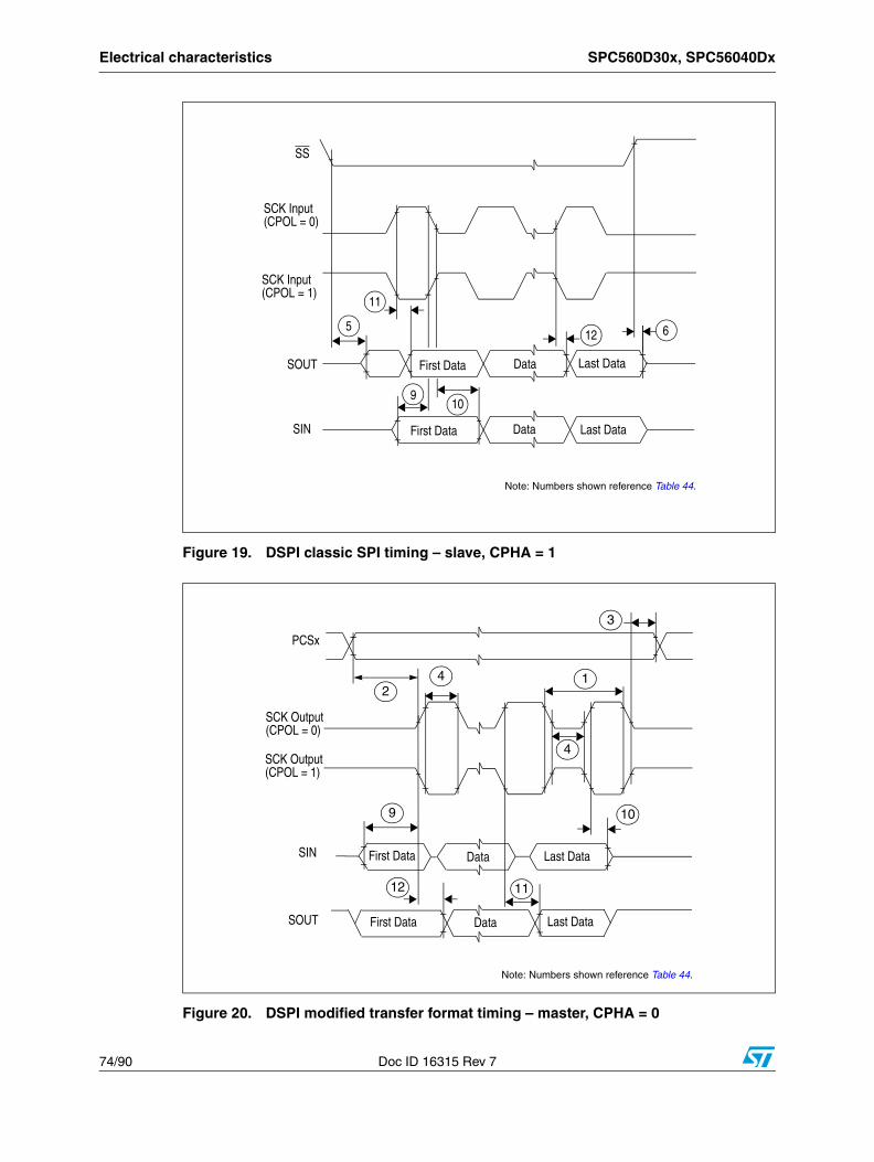
Electrical characteristics SPC560D30x, SPC56040Dx
74/90 Doc ID 16315 Rev 7
Figure 19. DSPI classic SPI timing – slave, CPHA = 1
Figure 20. DSPI modified transfer format timing – master, CPHA = 0
5 6
9
12
11
10
Last Data
Last DataSIN
SOUT
SS
First Data
First Data
Data
Data
SCK Input
SCK Input
(CPOL = 0)
(CPOL = 1)
Note: Numbers shown reference Table 44.
PCSx
3
14
10
4
9
12 11
SCK Output
SCK Output
SIN
SOUT
First Data Data Last Data
First Data Data Last Data
2
(CPOL = 0)
(CPOL = 1)
Note: Numbers shown reference Table 44.

SPC560D30x, SPC56040Dx Electrical characteristics
Doc ID 16315 Rev 7 75/90
Figure 21. DSPI modified transfer format timing – master, CPHA = 1
Figure 22. DSPI modified transfer format timing – slave, CPHA = 0
PCSx
109
12 11
SCK Output
SCK Output
SIN
SOUT
First Data Data Last Data
First Data Data Last Data
(CPOL = 0)
(CPOL = 1)
Note: Numbers shown reference Table 44.
Last DataFirst Data
3
4
1
Data
Data
SIN
SOUT
SS
4
5 6
9
11
10
SCK Input
First Data Last Data
SCK Input
2
(CPOL = 0)
(CPOL = 1)
12
Note: Numbers shown reference Table 44.

Electrical characteristics SPC560D30x, SPC56040Dx
76/90 Doc ID 16315 Rev 7
Figure 23. DSPI modified transfer format timing – slave, CPHA = 1
Figure 24. DSPI PCS strobe (PCSS) timing
5 6
9
12
11
10
Last Data
Last DataSIN
SOUT
SS
First Data
First Data
Data
Data
SCK Input
SCK Input
(CPOL = 0)
(CPOL = 1)
Note: Numbers shown reference Table 44.
PCSx
7 8
PCSS
Note: Numbers shown reference Table 44.

SPC560D30x, SPC56040Dx Electrical characteristics
Doc ID 16315 Rev 7 77/90
4.18.3 JTAG characteristics
Figure 25. Timing diagram – JTAG boundary scan
Table 45. JTAG characteristics
No. Symbol C ParameterValue
UnitMin Typ Max
1 tJCYC CC D TCK cycle time 83.33 — — ns
2 tTDIS CC D TDI setup time 15 — — ns
3 tTDIH CC D TDI hold time 5 — — ns
4 tTMSS CC D TMS setup time 15 — — ns
5 tTMSH CC D TMS hold time 5 — — ns
6 tTDOV CC D TCK low to TDO valid — — 49 ns
7 tTDOI CC D TCK low to TDO invalid 6 — — ns
INPUT DATA VALID
OUTPUT DATA VALID
DATA INPUTS
DATA OUTPUTS
DATA OUTPUTS
TCK
Note: Numbers shown reference Table 45.
3/52/4
7
6
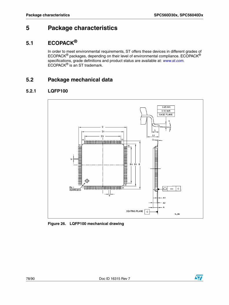
Package characteristics SPC560D30x, SPC56040Dx
78/90 Doc ID 16315 Rev 7
5 Package characteristics
5.1 ECOPACK®
In order to meet environmental requirements, ST offers these devices in different grades of ECOPACK® packages, depending on their level of environmental compliance. ECOPACK® specifications, grade definitions and product status are available at: www.st.com. ECOPACK® is an ST trademark.
5.2 Package mechanical data
5.2.1 LQFP100
Figure 26. LQFP100 mechanical drawing

SPC560D30x, SPC56040Dx Package characteristics
Doc ID 16315 Rev 7 79/90
Table 46. LQFP100 mechanical data
Symbolmm inches(1)
Min Typ Max Min Typ Max
A — — 1.600 — — 0.0630
A1 0.050 — 0.150 0.0020 — 0.0059
A2 1.350 1.400 1.450 0.0531 0.0551 0.0571
b 0.170 0.220 0.270 0.0067 0.0087 0.0106
c 0.090 — 0.200 0.0035 — 0.0079
D 15.800 16.000 16.200 0.6220 0.6299 0.6378
D1 13.800 14.000 14.200 0.5433 0.5512 0.5591
D3 — 12.000 — — 0.4724 —
E 15.800 16.000 16.200 0.6220 0.6299 0.6378
E1 13.800 14.000 14.200 0.5433 0.5512 0.5591
E3 — 12.000 — — 0.4724 —
e — 0.500 — — 0.0197 —
L 0.450 0.600 0.750 0.0177 0.0236 0.0295
L1 — 1.000 — — 0.0394 —
k 0.0 ° 3.5 ° 7.0 ° 0.0 ° 3.5 ° 7.0 °
Tolerance mm inches
ccc 0.080 0.0031
1. Values in inches are converted from mm and rounded to 4 decimal digits.

Package characteristics SPC560D30x, SPC56040Dx
80/90 Doc ID 16315 Rev 7
5.2.2 LQFP64
Figure 27. LQFP64 mechanical drawing
5W_ME
LA1 K
L1
c
AA2
ccc C
D
D1
D3
E3 E1 E
32
3348
49
b
64
1
Pin 1identification 16
17
Table 47. LQFP64 mechanical data
Symbolmm inches(1)
Min Typ Max Min Typ Max
A — — 1.6 — — 0.0630
A1 0.05 — 0.15 0.0020 — 0.0059
A2 1.35 1.4 1.45 0.0531 0.0551 0.0571
b 0.17 0.22 0.27 0.0067 0.0087 0.0106
c 0.09 — 0.2 0.0035 — 0.0079
D 11.8 12 12.2 0.4646 0.4724 0.4803
D1 9.8 10 10.2 0.3858 0.3937 0.4016
D3 — 7.5 — — 0.2953 —
E 11.8 12 12.2 0.4646 0.4724 0.4803
E1 9.8 10 10.2 0.3858 0.3937 0.4016
E3 — 7.5 — — 0.2953 —
e — 0.5 — — 0.0197 —
L 0.45 0.6 0.75 0.0177 0.0236 0.0295
L1 — 1 — — 0.0394 —

SPC560D30x, SPC56040Dx Package characteristics
Doc ID 16315 Rev 7 81/90
k 0.0° 3.5° 7.0° 0.0° 3.5° 7.0°
ccc — — 0.08 — — 0.0031
1. Values in inches are converted from mm and rounded to 4 decimal digits.
Table 47. LQFP64 mechanical data (continued)
Symbolmm inches(1)
Min Typ Max Min Typ Max
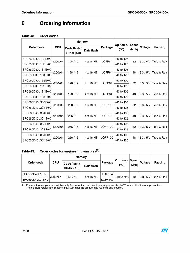
Ordering information SPC560D30x, SPC56040Dx
82/90 Doc ID 16315 Rev 7
6 Ordering information
Table 48. Order codes
Order code CPU
Memory
PackageOp. temp.
(°C)
Speed
(MHz)Voltage PackingCode flash /
SRAM (KB)Data flash
SPC560D30L1B3E0Xe200z0h 128 / 12 4 x 16 KB LQFP64
40 to 10532 3.3 / 5 V Tape & Reel
SPC560D30L1C3E0X 40 to 125
SPC560D30L1B4E0Xe200z0h 128 / 12 4 x 16 KB LQFP64
40 to 10548 3.3 / 5 V Tape & Reel
SPC560D30L1C4E0X 40 to 125
SPC560D30L1B3E0Xe200z0h 128 / 12 4 x 16 KB LQFP64
40 to 10532 3.3 / 5 V Tape & Reel
SPC560D30L1C3E0X 40 to 125
SPC560D30L1B4E0Xe200z0h 128 / 12 4 x 16 KB LQFP64
40 to 10548 3.3 / 5 V Tape & Reel
SPC560D30L1C4E0X 40 to 125
SPC560D40L3B3E0Xe200z0h 256 / 16 4 x 16 KB LQFP100
40 to 10532 3.3 / 5 V Tape & Reel
SPC560D40L3C3E0X 40 to 125
SPC560D40L3B4E0Xe200z0h 256 / 16 4 x 16 KB LQFP100
40 to 10548 3.3 / 5 V Tape & Reel
SPC560D40L3C4E0X 40 to 125
SPC560D40L3B3E0Xe200z0h 256 / 16 4 x 16 KB LQFP100
40 to 10532 3.3 / 5 V Tape & Reel
SPC560D40L3C3E0X 40 to 125
SPC560D40L3B4E0Xe200z0h 256 / 16 4 x 16 KB LQFP100
40 to 10548 3.3 / 5 V Tape & Reel
SPC560D40L3C4E0X 40 to 125
Table 49. Order codes for engineering samples(1)
Order code CPU
Memory
PackageOp. temp.
(°C)
Speed
(MHz)Voltage PackingCode flash /
SRAM (KB)Data flash
SPC560D40L1-ENGe200z0h 256 / 16 4 x 16 KB
LQFP6440 to 125 48 3.3 / 5 V Tape & Reel
SPC560D40L3-ENG LQFP100
1. Engineering samples are suitable only for evaluation and development purpose but NOT for qualification and production. Their silicon version and maturity may vary until the product has reached qualification.

SPC560D30x, SPC56040Dx Ordering information
Doc ID 16315 Rev 7 83/90
Figure 28. Commercial product code structure
Memory PackingCore Family
Y = Tray
X = Tape and Reel 90°
3E0 = 32 MHz EEPROM 5V/3V
4E0 = 48 MHz EEPROM 5V/3V
B = –40 to 105 °CC = –40 to 125 °C
L1 = LQFP64
L3 = LQFP100
40 = 256 KB
30 = 128 KB
D = Access family
0 = e200z0h
SPC56 = Power Architecture in 90 nm
TemperaturePackage Custom versionSPC56 40 Y0 D CL3 4E0
Example code:
Product identifier

Ordering information SPC560D30x, SPC56040Dx
84/90 Doc ID 16315 Rev 7
Appendix A Abbreviations
Table 50 lists abbreviations used in this document.
Table 50. Abbreviations
Abbreviation Meaning
APU Auxilliary processing unit
CMOS Complementary metal–oxide–semiconductor
CPHA Clock phase
CPOL Clock polarity
CS Peripheral chip select
DAOC Double action output compare
ECC Error code correction
EVTO Event out
GPIO General purpose input/output
IPM Input period measurement
IPWM Input pulse width measurement
MB Message buffer
MC Modulus counter
MCB Modulus counter buffered (up / down)
MCKO Message clock out
MDO Message data out
MSEO Message start/end out
MTFE Modified timing format enable
NVUSRO Non-volatile user options register
OPWFMB Output pulse width and frequency modulation buffered
OPWMB Output pulse width modulation buffered
OPWMCB Center aligned output pulse width modulation buffered with dead time
OPWMT Output pulse width modulation trigger
PWM Pulse width modulation
SAIC Single action input capture
SAOC Single action output compare
SCK Serial communications clock
SOUT Serial data out
TBD To be defined
TCK Test clock input
TDI Test data input

SPC560D30x, SPC56040Dx Ordering information
Doc ID 16315 Rev 7 85/90
TDO Test data output
TMS Test mode select
Table 50. Abbreviations (continued)
Abbreviation Meaning

Revision history SPC560D30x, SPC560D40x
86/90 Doc ID 16315 Rev 7
Revision history
Table 51 summarizes revisions to this document.
Table 51. Document revision history
Date Revision Changes
09-Jul-2009 1 Initial release.
18-Feb-2010 2
Updated the following tables:- Absolute maximum ratings- Low voltage power domain electrical characteristics;- On-chip peripherals current consumption- DSPI characteristics;- JTAG characteristics;- ADC conversion characteristics;
Inserted a note on “Flash power supply DC characteristics” section.
10-Aug-2010 3
“Features” section: Updated information concerning eMIOS, ADC, LINFlex, Nexus and low power capabilities
“Pictus 512K device comparison” table: updated the “Execution speed” row
“Pictus 512K series block diagram” figure:
– updated max number of Crossbar Switches– updated Legend
“Pictus 512K series block summary” table: added contents concernig the eDMA block
“LQFP100 pin configuration (top view)” figure:
– removed alternate functions– updated supply pins
“LQFP64 pin configuration (top view)” figure: removed alternate functions
Added “Pin muxing” section
“NVUSRO register” section: Deleted “NVUSRO[WATCHDOG_EN] field description“ section
“Recommended operating conditions (3.3 V)” table:– TVDD: deleted min value
– In footnote No. 3, changed capacitance value between VDD_BV and VSS_LV
“Recommended operating conditions (5.0 V)” table: deleted TVDD min value“LQFP thermal characteristics” table: changed RJC values
“I/O input DC electrical characteristics” table:
– WFI: updated max value– WNFI: updated min value
“I/O consumption” table: removed IDYNSEG row
Added “I/O weight” table“Program and erase specifications (Code Flash)” table: deleted TBank_C row

SPC560D30x, SPC560D40x Revision history
Doc ID 16315 Rev 7 87/90
10-Aug-20103
(cont.)
Updated the following tables:
– “Voltage regulator electrical characteristics”– “Low voltage monitor electrical characteristics”
– “Low voltage power domain electrical characteristics”
– “Start-up time/Switch-off time”– “Fast external crystal oscillator (4 to 16 MHz) electrical
characteristics”– “FMPLL electrical characteristics”
– “Fast internal RC oscillator (16 MHz) electrical characteristics”
– “ADC conversion characteristics”– “On-chip peripherals current consumption”
– “DSPI characteristics”
“DSPI characteristics” section: removed “DSPI PCS strobe (PCSS) timing” figure
Updated “Order codes” tableAdded “Order codes for engineering samples” table
Updated “Commercial product code structure” table
16-Sep-2011 4
Formatting and editorial changes throughout
Device comparison table: for the “Total timer I/O eMIOS”, changed “13 ch” to “14 ch”
SPC560D30/SPC560D40 series block summary:– added definition for “AUTOSAR” acronym
– changed “System watchdog timer” to “Software watchdog timer”
LQFP64 pin configuration (top view): changed pin 6 from VPP_TEST to VSS_HV
Added section “Pad configuration during reset phases”Added section “Voltage supply pins”
Added section “Pad types”
Added section “System pins”Renamed and updated section “Functional ports” (was previously section “Pin muxing”); update includes replacing all instances of WKUP with WKPU (WKPU is the correct abbreviation for Wakeup Unit)
Section “NVUSRO register”: edited content to separate configuration into electrical parameters and digital functionalityAdded section “NVUSRO[WATCHDOG_EN] field description”
Absolute maximum ratings: Removed “C” column from table
Replaced “TBD” with “—” in TVDD min value cell of 3.3 V and 5 V recommended operating conditions tables
LQFP thermal characteristics: removed RJB single layer board conditions; updated footnote 4
I/O input DC electrical characteristics: removed footnote “All values need to be confirmed during device validation”; updated ILKG characteristics
Table 51. Document revision history (continued)
Date Revision Changes

Revision history SPC560D30x, SPC560D40x
88/90 Doc ID 16315 Rev 7
16-Sep-20114
(cont.)
MEDIUM configuration output buffer electrical characteristics: changed “IOH = 100 µA” to “IOL = 100 µA” in VOL conditions
I/O consumption: replaced instances of “Root medium square” with “Root mean square”
Updated section “Voltage regulator electrical characteristics”
Section “Low voltage detector electrical characteristics”: changed title (was “Voltage monitor electrical characteristics”); added a fifth LVD (LVDHV3B); added event status flag names found in RGM chapter of device reference manual to POR module and LVD descriptions; replaced instances of “Low voltage monitor” with “Low voltage detector”; deleted note referencing power domain No. 2 (this domain is not present on the device); updated electrical characteristics table
Updated and renamed section “Power consumption” (was previously section “Low voltage domain power consumption”)
Program and erase specifications (code flash): updated symbols; updated tesus values
Updated Flash memory read access timingEMI radiated emission measurement: updated SEMI values
Updated FMPLL electrical characteristics
Crystal oscillator and resonator connection scheme: inserted footnote about possibly requiring a series resistorFast internal RC oscillator (16 MHz) electrical characteristics: updated tFIRCSU valuesSection “Input impedance and ADC accuracy”: changed “VA/VA2” to “VA2/VA” in Equation 13ADC conversion characteristics:
– updated conditions for sampling time VDD = 5.0 V
– updated conditions for conversion time VDD = 5.0 V
Updated Abbreviations
Removed Order codes tables.
01-Dec-2011 5Replaced “TBD” with “8.21 mA” in IDD_HV(FLASH) cell of On-chip peripherals current consumption table
Table 51. Document revision history (continued)
Date Revision Changes

SPC560D30x, SPC560D40x Revision history
Doc ID 16315 Rev 7 89/90
04-Feb-2013 6
Removed all instances of table footnote “All values need to be confirmed during device validation”
Section 4.1, Introduction, removed Caution note.
Table 11 (Recommended operating conditions (3.3 V)), added minimum value of TVDD and footnote about it.
Table 12 (Recommended operating conditions (5.0 V)), added minimum value of TVDD and footnote about it.
Updated Section 4.17.2, Input impedance and ADC accuracyIn Table 24, changed VLVDHV3L, VLVDHV3BL from 2.7 V to 2.6 V. Revised the Table 28 (Flash module life)Updated Table 43, DSPI characteristics, to add specifications 7 and
8, tPCSC and tPASC.
Inserted Figure 24, DSPI PCS strobe (PCSS) timing.
17-Sep-2013 7 Updated Disclaimer.
Table 51. Document revision history (continued)
Date Revision Changes

SPC560D30x, SPC56040Dx
90/90 Doc ID 16315 Rev 7
Please Read Carefully:
Information in this document is provided solely in connection with ST products. STMicroelectronics NV and its subsidiaries (“ST”) reserve theright to make changes, corrections, modifications or improvements, to this document, and the products and services described herein at anytime, without notice.
All ST products are sold pursuant to ST’s terms and conditions of sale.
Purchasers are solely responsible for the choice, selection and use of the ST products and services described herein, and ST assumes noliability whatsoever relating to the choice, selection or use of the ST products and services described herein.
No license, express or implied, by estoppel or otherwise, to any intellectual property rights is granted under this document. If any part of thisdocument refers to any third party products or services it shall not be deemed a license grant by ST for the use of such third party productsor services, or any intellectual property contained therein or considered as a warranty covering the use in any manner whatsoever of suchthird party products or services or any intellectual property contained therein.
UNLESS OTHERWISE SET FORTH IN ST’S TERMS AND CONDITIONS OF SALE ST DISCLAIMS ANY EXPRESS OR IMPLIED WARRANTY WITH RESPECT TO THE USE AND/OR SALE OF ST PRODUCTS INCLUDING WITHOUT LIMITATION IMPLIED WARRANTIES OF MERCHANTABILITY, FITNESS FOR A PARTICULAR PURPOSE (AND THEIR EQUIVALENTS UNDER THE LAWS OF ANY JURISDICTION), OR INFRINGEMENT OF ANY PATENT, COPYRIGHT OR OTHER INTELLECTUAL PROPERTY RIGHT.
ST PRODUCTS ARE NOT DESIGNED OR AUTHORIZED FOR USE IN: (A) SAFETY CRITICAL APPLICATIONS SUCH AS LIFE SUPPORTING, ACTIVE IMPLANTED DEVICES OR SYSTEMS WITH PRODUCT FUNCTIONAL SAFETY REQUIREMENTS; (B) AERONAUTIC APPLICATIONS; (C) AUTOMOTIVE APPLICATIONS OR ENVIRONMENTS, AND/OR (D) AEROSPACE APPLICATIONS OR ENVIRONMENTS. WHERE ST PRODUCTS ARE NOT DESIGNED FOR SUCH USE, THE PURCHASER SHALL USE PRODUCTS AT PURCHASER’S SOLE RISK, EVEN IF ST HAS BEEN INFORMED IN WRITING OF SUCH USAGE, UNLESS A PRODUCT IS EXPRESSLY DESIGNATED BY ST AS BEING INTENDED FOR “AUTOMOTIVE, AUTOMOTIVE SAFETY OR MEDICAL” INDUSTRY DOMAINS ACCORDING TO ST PRODUCT DESIGN SPECIFICATIONS. PRODUCTS FORMALLY ESCC, QML OR JAN QUALIFIED ARE DEEMED SUITABLE FOR USE IN AEROSPACE BY THE CORRESPONDING GOVERNMENTAL AGENCY.
Resale of ST products with provisions different from the statements and/or technical features set forth in this document shall immediately voidany warranty granted by ST for the ST product or service described herein and shall not create or extend in any manner whatsoever, anyliability of ST.
ST and the ST logo are trademarks or registered trademarks of ST in various countries.Information in this document supersedes and replaces all information previously supplied.
The ST logo is a registered trademark of STMicroelectronics. All other names are the property of their respective owners.
© 2013 STMicroelectronics - All rights reserved
STMicroelectronics group of companies
Australia - Belgium - Brazil - Canada - China - Czech Republic - Finland - France - Germany - Hong Kong - India - Israel - Italy - Japan - Malaysia - Malta - Morocco - Philippines - Singapore - Spain - Sweden - Switzerland - United Kingdom - United States of America
www.st.com