Embed Size (px)
Citation preview

8/8/2019 2.CMOS FAbri
http://slidepdf.com/reader/full/2cmos-fabri 1/17
2.1 Introduction
In this chapter, the fundamentals of MOS chip fabrication will be discussed and the major steps of the process
flow will be examined. It is not the aim of this chapter to present a detailed discussion of silicon fabrication
technology, which deserves separate treatment in a dedicated course. Rather, the emphasis will be on thegeneral outline of the process flow and on the interaction of various processing steps, which ultimately
determine the device and the circuit performance characteristics. The following chapters show that there are
very strong links between the fabrication process, the circuit design process and the performance of the
resulting chip. Hence, circuit designers must have a working knowledge of chip fabrication to create effectivedesigns and in order to optimize the circuits with respect to various manufacturing parameters. Also, the circuit
designer must have a clear understanding of the roles of various masks used in the fabrication process, and howthe masks are used to define various features of the devices on-chip.
The following discussion will concentrate on the well-established CMOS fabrication technology, whichrequires that both n-channel (nMOS) and p-channel (pMOS) transistors be built on the same chip substrate. To
accommodate both nMOS and pMOS devices, special regions must be created in which the semiconductor type
is opposite to the substrate type. These regions are called wells or tubs. A p-well is created in an n-type
substrate or, alternatively, an n- well is created in a p-type substrate. In the simple n-well CMOS fabricationtechnology presented, the nMOS transistor is created in the p-type substrate, and the pMOS transistor is created
in the n-well, which is built-in into the p-type substrate. In the twin-tub CMOS technology, additional tubs of the same type as the substrate can also be created for device optimization.
The simplified process sequence for the fabrication of CMOS integrated circuits on a p- type silicon substrate is
shown in Fig. 2.1. The process starts with the creation of the n-well regions for pMOS transistors, by impurityimplantation into the substrate. Then, a thick oxide is grown in the regions surrounding the nMOS and pMOS
active regions. The thin gate oxide is subsequently grown on the surface through thermal oxidation. These steps
are followed by the creation of n+ and p+ regions (source, drain and channel-stop implants) and by final
metallization (creation of metal interconnects).
The process flow sequence pictured in Fig. 2.1 may at first seem to be too abstract, since detailed fabrication
steps are not shown. To obtain a better understanding of the issues involved in the semiconductor fabricationprocess, we first have to consider some of the basic steps in more detail.
2.2 Fabrication Process Flow - Basic Steps
Note that each processing step requires that certain areas are defined on chip by appropriate masks.
Consequently, the integrated circuit may be viewed as a set of patterned layers of doped silicon, polysilicon,metal and insulating silicon dioxide. In general, a layer must be patterned before the next layer of material is
applied on chip. The process used to transfer a pattern to a layer on the chip is called lithography. Since each
layer has its own distinct patterning requirements, the lithographic sequence must be repeated for every layer,
using a different mask.
To illustrate the fabrication steps involved in patterning silicon dioxide through optical lithography, let us first
examine the process flow shown in Fig. 2.2. The sequence starts with the thermal oxidation of the siliconsurface, by which an oxide layer of about 1 micrometer thickness, for example, is created on the substrate (Fig.
2.2(b)). The entire oxide surface is then covered with a layer of photoresist, which is essentially a light-
sensitive, acid-resistant organic polymer, initially insoluble in the developing solution (Fig. 2.2(c)). If thephotoresist material is exposed to ultraviolet (UV) light, the exposed areas become soluble so that the they are
no longer resistant to etching solvents. To selectively expose the photoresist, we have to cover some of the areas
on the surface with a mask during exposure. Thus, when the structure with the mask on top is exposed to UV

8/8/2019 2.CMOS FAbri
http://slidepdf.com/reader/full/2cmos-fabri 2/17
light, areas which are covered by the opaque features on the mask are shielded. In the areas where the UV lightcan pass through, on the other hand, the photoresist is exposed and becomes soluble (Fig. 2.2(d)).
Figure-2.1: Simplified process sequence for fabrication of the n-well CMOS integrated circuit with a single
polysilicon layer, showing only major fabrication steps.
The type of photoresist which is initially insoluble and becomes soluble after exposure to UV light is called
positive photoresist. The process sequence shown in Fig. 2.2 uses positive photoresist. There is another type of photoresist which is initially soluble and becomes insoluble (hardened) after exposure to UV light, called
negative photoresist. If negative photoresist is used in the photolithography process, the areas which are notshielded from the UV light by the opaque mask features become insoluble, whereas the shielded areas can
subsequently be etched away by a developing solution. Negative photoresists are more sensitive to light, buttheir photolithographic resolution is not as high as that of the positive photoresists. Therefore, negative
photoresists are used less commonly in the manufacturing of high-density integrated circuits.

8/8/2019 2.CMOS FAbri
http://slidepdf.com/reader/full/2cmos-fabri 3/17
igure-2.2: Process steps required for patterning of silicon dioxide.

8/8/2019 2.CMOS FAbri
http://slidepdf.com/reader/full/2cmos-fabri 4/17
Following the UV exposure step, the unexposed portions of the photoresist can be removed by a solvent. Now,the silicon dioxide regions which are not covered by hardened photoresist can be etched away either by using a
chemical solvent (HF acid) or by using a dry etch (plasma etch) process (Fig. 2.2(e)). Note that at the end of this
step, we obtain an oxide window that reaches down to the silicon surface (Fig. 2.2(f)). The remainingphotoresist can now be stripped from the silicon dioxide surface by using another solvent, leaving the patterned
silicon dioxide feature on the surface as shown in Fig. 2.2(g).
The sequence of process steps illustrated in detail in Fig. 2.2 actually accomplishes a single pattern transfer onto
the silicon dioxide surface, as shown in Fig. 2.3. The fabrication of semiconductor devices requires several suchpattern transfers to be performed on silicon dioxide, polysilicon, and metal. The basic patterning process used inall fabrication steps, however, is quite similar to the one shown in Fig. 2.2. Also note that for accurate
generation of high-density patterns required in sub-micron devices, electron beam (E-beam) lithography is used
instead of optical lithography. In the following, the main processing steps involved in the fabrication of an n-
channel MOS transistor on p-type silicon substrate will be examined.
Figure-2.3: The result of a single lithographic patterning sequence on silicon dioxide, without showing the
intermediate steps. Compare the unpatterned structure (top) and the patterned structure (bottom) with Fig. 2.2(b)
and Fig. 2.2(g), respectively.
The process starts with the oxidation of the silicon substrate (Fig. 2.4(a)), in which a relatively thick silicondioxide layer, also called field oxide, is created on the surface (Fig. 2.4(b)). Then, the field oxide is selectively
etched to expose the silicon surface on which the MOS transistor will be created (Fig. 2.4(c)). Following thisstep, the surface is covered with a thin, high-quality oxide layer, which will eventually form the gate oxide of
the MOS transistor (Fig. 2.4(d)). On top of the thin oxide, a layer of polysilicon (polycrystalline silicon) is
deposited (Fig. 2.4(e)). Polysilicon is used both as gate electrode material for MOS transistors and also as an
interconnect medium in silicon integrated circuits. Undoped polysilicon has relatively high resistivity. Theresistivity of polysilicon can be reduced, however, by doping it with impurity atoms.
After deposition, the polysilicon layer is patterned and etched to form the interconnects and the MOS transistor
gates (Fig. 2.4(f)). The thin gate oxide not covered by polysilicon is also etched away, which exposes the bare
silicon surface on which the source and drain junctions are to be formed (Fig. 2.4(g)). The entire silicon surface
is then doped with a high concentration of impurities, either through diffusion or ion implantation (in this casewith donor atoms to produce n-type doping). Figure 2.4(h) shows that the doping penetrates the exposed areas
on the silicon surface, ultimately creating two n-type regions (source and drain junctions) in the p-type
substrate. The impurity doping also penetrates the polysilicon on the surface, reducing its resistivity. Note thatthe polysilicon gate, which is patterned before doping actually defines the precise location of the channel region
8/8/2019 2.CMOS FAbri
http://slidepdf.com/reader/full/2cmos-fabri 5/17
and, hence, the location of the source and the drain regions. Since this procedure allows very precise positioningof the two regions relative to the gate, it is also called the self-aligned process.

8/8/2019 2.CMOS FAbri
http://slidepdf.com/reader/full/2cmos-fabri 6/17

8/8/2019 2.CMOS FAbri
http://slidepdf.com/reader/full/2cmos-fabri 7/17
igure-2.4: Process flow for the fabrication of an n-type MOSFET on p-type silicon.
Once the source and drain regions are completed, the entire surface is again covered with an insulating layer of
silicon dioxide (Fig. 2.4(i)). The insulating oxide layer is then patterned in order to provide contact windows forthe drain and source junctions (Fig. 2.4(j)). The surface is covered with evaporated aluminum which will form
the interconnects (Fig. 2.4(k)). Finally, the metal layer is patterned and etched, completing the interconnection
of the MOS transistors on the surface (Fig. 2.4(l)). Usually, a second (and third) layer of metallic interconnect
can also be added on top of this structure by creating another insulating oxide layer, cutting contact (via) holes,
depositing, and patterning the metal.
2.3 The CMOS n-Well Process
Having examined the basic process steps for pattern transfer through lithography, and having gone through thefabrication procedure of a single n-type MOS transistor, we can now return to the generalized fabrication
sequence of n-well CMOS integrated circuits, as shown in Fig. 2.1. In the following figures, some of the
important process steps involved in the fabrication of a CMOS inverter will be shown by a top view of the
lithographic masks and a cross-sectional view of the relevant areas.
The n-well CMOS process starts with a moderately doped (with impurity concentration typically less than 1015cm-3) p-type silicon substrate. Then, an initial oxide layer is grown on the entire surface. The first lithographicmask defines the n-well region. Donor atoms, usually phosphorus, are implanted through this window in the
oxide. Once the n-well is created, the active areas of the nMOS and pMOS transistors can be defined. Figures
2.5 through 2.10 illustrate the significant milestones that occur during the fabrication process of a CMOSinverter.

8/8/2019 2.CMOS FAbri
http://slidepdf.com/reader/full/2cmos-fabri 8/17
Figure-2.5: Following the creation of the n-well region, a thick field oxide is grown in the areas surroundingthe transistor active regions, and a thin gate oxide is grown on top of the active regions. The thickness and the
quality of the gate oxide are two of the most critical fabrication parameters, since they strongly affect the
operational characteristics of the MOS transistor, as well as its long-term reliability.

8/8/2019 2.CMOS FAbri
http://slidepdf.com/reader/full/2cmos-fabri 9/17
igure-2.6: The polysilicon layer is deposited using chemical vapor deposition (CVD) and patterned by dry
(plasma) etching. The created polysilicon lines will function as the gate electrodes of the nMOS and the pMOStransistors and their interconnects. Also, the polysilicon gates act as self-aligned masks for the source and drain
implantations that follow this step.

8/8/2019 2.CMOS FAbri
http://slidepdf.com/reader/full/2cmos-fabri 10/17

8/8/2019 2.CMOS FAbri
http://slidepdf.com/reader/full/2cmos-fabri 11/17
igure-2.8: An insulating silicon dioxide layer is deposited over the entire wafer using CVD. Then, the contactsare defined and etched away to expose the silicon or polysilicon contact windows. These contact windows are
necessary to complete the circuit interconnections using the metal layer, which is patterned in the next step.

8/8/2019 2.CMOS FAbri
http://slidepdf.com/reader/full/2cmos-fabri 12/17
igure-2.9: Metal (aluminum) is deposited over the entire chip surface using metal evaporation, and the metal
lines are patterned through etching. Since the wafer surface is non-planar, the quality and the integrity of the
metal lines created in this step are very critical and are ultimately essential for circuit reliability.

8/8/2019 2.CMOS FAbri
http://slidepdf.com/reader/full/2cmos-fabri 13/17
igure-2.10: The composite layout and the resulting cross-sectional view of the chip, showing one nMOS andone pMOS transistor (built-in n-well), the polysilicon and metal interconnections. The final step is to deposit the
passivation layer (for protection) over the chip, except for wire-bonding pad areas.

8/8/2019 2.CMOS FAbri
http://slidepdf.com/reader/full/2cmos-fabri 14/17
The patterning process by the use of a succession of masks and process steps is conceptually summarized inFig. 2.11. It is seen that a series of masking steps must be sequentially performed for the desired patterns to be
created on the wafer surface. An example of the end result of this sequence is shown as a cross-section on the
right.
Figure-2.11: Conceptual illustration of the mask sequence applied to create desired structures.
2.4 Advanced CMOS Fabrication Technologies
In this section, two examples will be given for advanced CMOS processes which offer additional benefits interms of device performance and integration density. These processes, namely, the twin-tub CMOS process and
the silicon-on-insulator (SOI) process, are becoming especially more popular for sub-micron geometries wheredevice performance and density must be pushed beyond the limits of the conventional n-well CMOS process.
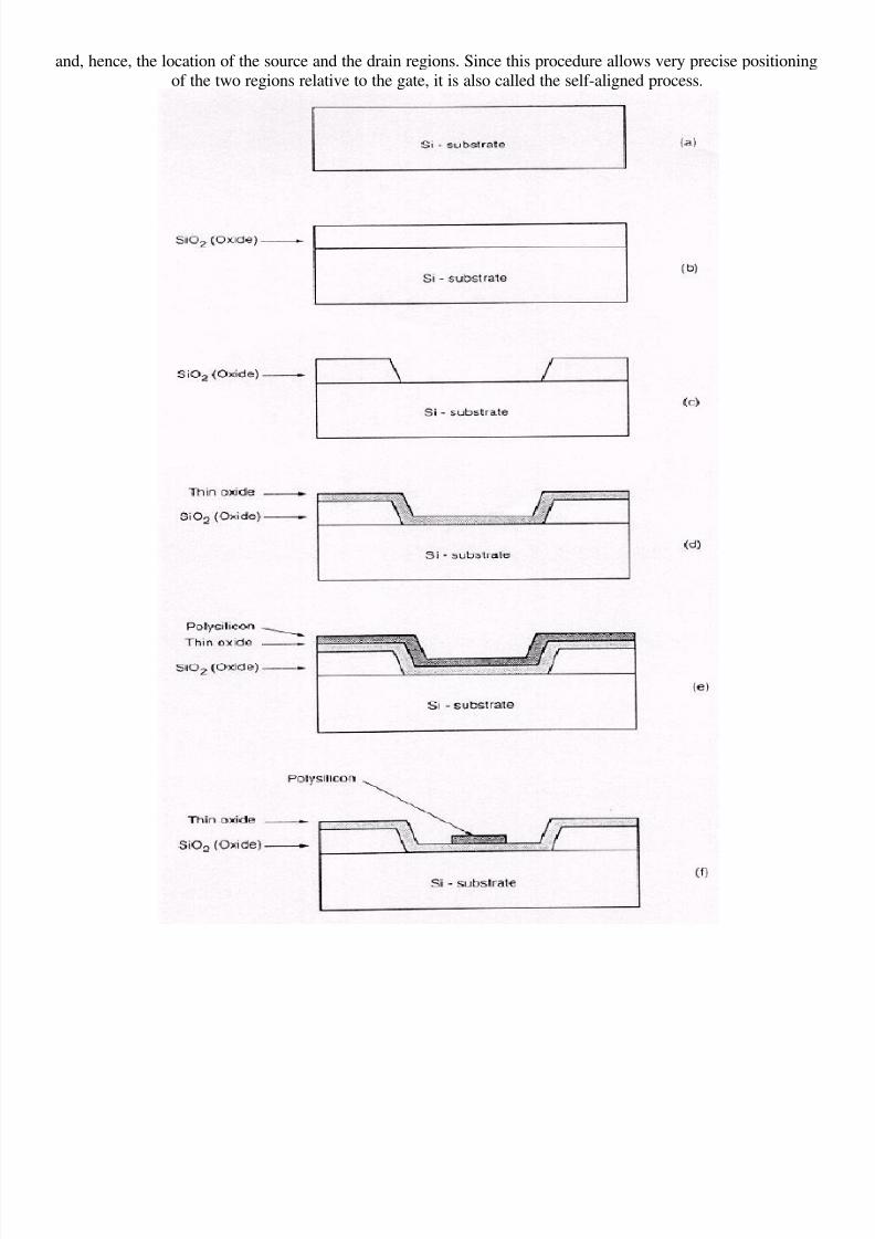
Twin-Tub (Twin-Well) CMOS Process
This technology provides the basis for separate optimization of the nMOS and pMOS transistors, thus making it
possible for threshold voltage, body effect and the channel transconductance of both types of transistors to betuned independently. Generally, the starting material is a n+ or p+ substrate, with a lightly doped epitaxial layer
on top. This epitaxial layer provides the actual substrate on which the n-well and the p-well are formed. Since
two independent doping steps are performed for the creation of the well regions, the dopant concentrations canbe carefully optimized to produce the desired device characteristics.
8/8/2019 2.CMOS FAbri
http://slidepdf.com/reader/full/2cmos-fabri 15/17
In the conventional n-well CMOS process, the doping density of the well region is typically about one order of magnitude higher than the substrate, which, among other effects, results in unbalanced drain parasitics. The
twin-tub process (Fig. 2.12) also avoids this problem.
Figure-2.12: Cross-section of nMOS and pMOS transistors in twin-tub CMOS process.
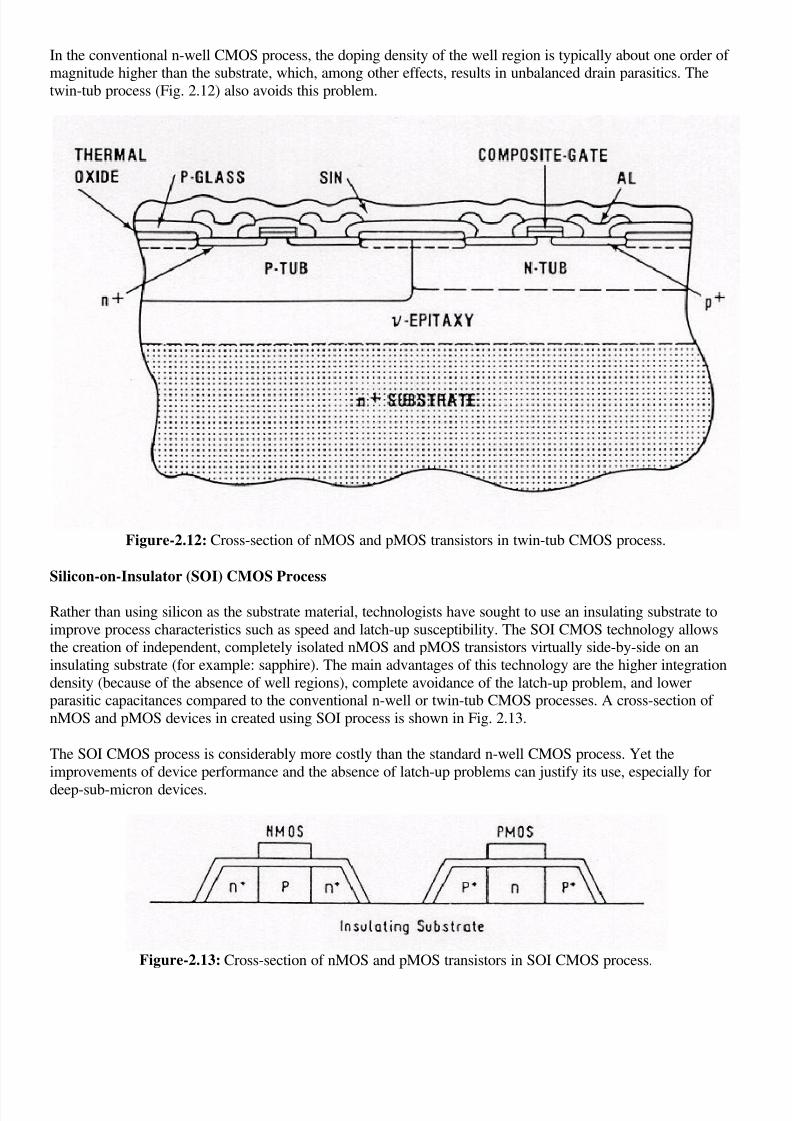
Silicon-on-Insulator (SOI) CMOS Process
Rather than using silicon as the substrate material, technologists have sought to use an insulating substrate to
improve process characteristics such as speed and latch-up susceptibility. The SOI CMOS technology allowsthe creation of independent, completely isolated nMOS and pMOS transistors virtually side-by-side on an
insulating substrate (for example: sapphire). The main advantages of this technology are the higher integration
density (because of the absence of well regions), complete avoidance of the latch-up problem, and lowerparasitic capacitances compared to the conventional n-well or twin-tub CMOS processes. A cross-section of
nMOS and pMOS devices in created using SOI process is shown in Fig. 2.13.
The SOI CMOS process is considerably more costly than the standard n-well CMOS process. Yet the
improvements of device performance and the absence of latch-up problems can justify its use, especially for
deep-sub-micron devices.
Figure-2.13: Cross-section of nMOS and pMOS transistors in SOI CMOS process.

8/8/2019 2.CMOS FAbri
http://slidepdf.com/reader/full/2cmos-fabri 16/17
2.5 Layout Design Rules
The physical mask layout of any circuit to be manufactured using a particular process must conform to a set of
geometric constraints or rules, which are generally called layout design rules. These rules usually specify the
minimum allowable line widths for physical objects on-chip such as metal and polysilicon interconnects ordiffusion areas, minimum feature dimensions, and minimum allowable separations between two such features.
If a metal line width is made too small, for example, it is possible for the line to break during the fabrication
process or afterwards, resulting in an open circuit. If two lines are placed too close to each other in the layout,
they may form an unwanted short circuit by merging during or after the fabrication process. The main objectiveof design rules is to achieve a high overall yield and reliability while using the smallest possible silicon area, for
any circuit to be manufactured with a particular process.
Note that there is usually a trade-off between higher yield which is obtained through conservative geometries,
and better area efficiency, which is obtained through aggressive, high- density placement of various features onthe chip. The layout design rules which are specified for a particular fabrication process normally represent a
reasonable optimum point in terms of yield and density. It must be emphasized, however, that the design rules
do not represent strict boundaries which separate "correct" designs from "incorrect" ones. A layout which
violates some of the specified design rules may still result in an operational circuit with reasonable yield,whereas another layout observing all specified design rules may result in a circuit which is not functional and/or
has very low yield. To summarize, we can say, in general, that observing the layout design rules significantlyincreases the probability of fabricating a successful product with high yield.
The design rules are usually described in two ways :
Micron rules, in which the layout constraints such as minimum feature sizes and minimum allowable
feature separations, are stated in terms of absolute dimensions in micrometers, or,
Lambda rules, which specify the layout constraints in terms of a single parameter (?) and, thus, allowlinear, proportional scaling of all geometrical constraints.
Lambda-based layout design rules were originally devised to simplify the industry- standard micron-based
design rules and to allow scaling capability for various processes. It must be emphasized, however, that most of the submicron CMOS process design rules do not lend themselves to straightforward linear scaling. The use of
lambda-based design rules must therefore be handled with caution in sub-micron geometries. In the following,we present a sample set of the lambda-based layout design rules devised for the MOSIS CMOS process and
illustrate the implications of these rules on a section a simple layout which includes two transistors (Fig. 2.14).
MOSIS Layout Design Rules (sample set)
Rule number Description L-Rule
R1 Minimum active area width 3 L
R2 Minimum active area spacing 3 L
R3 Minimum poly width 2 L
R4 Minimum poly spacing 2 L
R5 Minimum gate extension of poly over active 2 L
R6 Minimum poly-active edge spacing 1 L
(poly outside active area)
R7 Minimum poly-active edge spacing 3 L
(poly inside active area)

8/8/2019 2.CMOS FAbri
http://slidepdf.com/reader/full/2cmos-fabri 17/17
R8 Minimum metal width 3 L
R9 Minimum metal spacing 3 L
R10 Poly contact size 2 L
R11 Minimum poly contact spacing 2 L
R12 Minimum poly contact to poly edge spacing 1 L
R13 Minimum poly contact to metal edge spacing 1 L
R14 Minimum poly contact to active edge spacing 3 L
R15 Active contact size 2 L
R16 Minimum active contact spacing 2 L(on the same active region)
R17 Minimum active contact to active edge spacing 1 L
R18 Minimum active contact to metal edge spacing 1 L
R19 Minimum active contact to poly edge spacing 3 L
R20 Minimum active contact spacing 6 L
(on different active regions)
igure-2.14: Illustration of some of the typical MOSIS layout design rules listed above.