Embed Size (px)
Citation preview

29 May 2015
Carbon Nanotube Based Detectors for THz Radiometry
J.H. Lehman Na#onal Ins#tute of Standards and Technology 325 Broadway, Boulder, Colorado 80305-‐3228

Where and Who
Physical Measurement Laboratory Quantum Electronics and Photonics Division
Gaithersburg, MD
Boulder, CO
Nathan Tomlin, Malcolm White, Solomon Woods

Andreas Steiger, ChrisFan Monte, Jörg Hollandt Physikalisch-‐Technische Bundesanstalt, Berlin, Germany Free field, FTIR & far infrared/THz
Future
PTB - Berlin, Germany
Photo: A. Steiger

Single-wall Carbon Nanotubes
Multi-wall Carbon Nanotubes
Single sheet of graphene wrapped into a tube: microns in length, ~1-2 nm diameter, capped (Iijima, 1993).
Concentric cylinders of graphite with a hollow center, capped (Iijima, 1991)
Carbon Nanotubes
Not spectrally uniform
Very spectrally uniform

Nanotube topologies
mats
arrays
composite
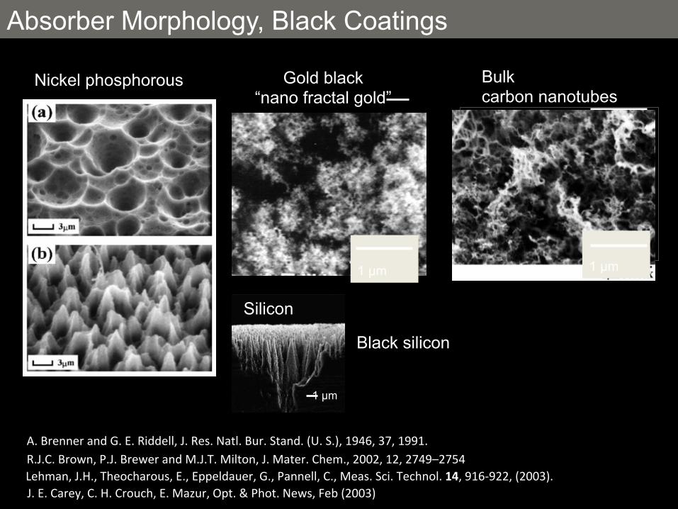
R.J.C. Brown, P.J. Brewer and M.J.T. Milton, J. Mater. Chem., 2002, 12, 2749–2754 A. Brenner and G. E. Riddell, J. Res. Natl. Bur. Stand. (U. S.), 1946, 37, 1991.
Nickel phosphorous Gold black “nano fractal gold”
1 µm
Lehman, J.H., Theocharous, E., Eppeldauer, G., Pannell, C., Meas. Sci. Technol. 14, 916-‐922, (2003).
1 µm
1 µm
Bulk carbon nanotubes
Absorber Morphology, Black Coatings
Silicon
1 µm
J. E. Carey, C. H. Crouch, E. Mazur, Opt. & Phot. News, Feb (2003)
Black silicon

Absorber Properties
1. index ~ air (or vacuum)
α =kρc
3. Thermal diffusivity large
k ~ 400 W/mK (big!) ρ ~ 7 kg/m3 (small!) c ~ 400 J/kgK
2. “Optically thick”
Lehman et al., Applied Optics, 50, 4099-4104, (2011)

~ 10 µm
r ~ 5 nm
s > 10 nm
* García-Vidal, et al., Phys. Rev. Lett., 78, 4289-4292 (1997)
s polarization, E directed along tube (optical response depends only on ε┴ for graphite)
p polarization, E perpendicular to tube (optical response depends on ε║ and ε┴ for graphite)
EMA for Aligned Cylinders

310 410 510 610 710Wavelength (nm)
70
75
80
85
90
95
100
Rel
ativ
e R
espo
nsiv
ity (%
)
low fill, large spacing
high fill, small spacing
spacing = 30 nm spacing = 17 nm
spacing = 14 nm
Based on index calculated from composite dielectric function; 60 µm thick, LiTaO3, with nickel electrodes
EMA, Calculated Results
Theocharous, et al., 45, APPL. OPT. 1093-‐1097 (2006)

Author's personal copy
unexposed to serve as the control and the other samples wereexposed to an oxygen plasma using a commercial plasmasystem. The settings used for the oxygen plasma treatmentwere a flow rate of 50 sccm O2, pressure of 32 Pa (0.24 T), RFpower of 50–200 W at 30 kHz, and duration of 15–300 s.
2.1. Specular reflectance
To measure the specular reflectance of the samples, we used
a commercial spectrophotometer with an accessory for mea-suring absolute specular reflectance. The incident light spotsize on the sample was 4 mm by 4 mm and an integrationtime of 1 s was used for each data point. A reference scan thatdid not reflect off the sample was used to convert the rawdetector data to absolute reflectance. Since the specularreflectance of the samples is so small, the signal is very smalland noisy, and only becomes appreciable at large incidenceangles. We have not fully evaluated the uncertainty of themeasurements, but believe it is roughly 0.005 (k = 2) due toinstrument drift and uncertainties in gains. Specular reflec-
tance at an incident angle of 65! from normal is shown inFig. 1. The plasma-treated samples all show lower specularreflectance over the whole measured wavelength range, withup to 5 times lower reflectance at long wavelengths.
2.2. Total hemispherical reflectance
To measure the total hemispherical reflectance of the samples,we used the same commercial spectrophotometer with a
150 mm diameter integrating sphere accessory. Samples wereheld at the back of the sphere against a 18 mm diameter port,tilted at 8! from normal incidence. The incident light spot sizeon the samples was 7.5 mm by 15 mm, the slit width was5 mm, each data point was integrated for 1 s, and three separatescans were averaged together. Background scans were used to
account for any stray light in the sphere and a calibrated stan-dard black reference material1 was used to convert the rawdetector data to absolute reflectance. The total hemisphericalreflectance is shown in Fig. 2. The plasma-treated samples showlower total reflectance over the whole measured wavelengthrange, with up to 8 times lower reflectance at short wavelengths.
2.3. Etch rate
We observed a linear decrease in height of the VACNT withplasma exposure. Using a commercial digital contact sensor
attached to the vertical axis of an optical microscope, wemeasured an etch rate of " 20 lm/min with an uncertaintyof 50 lm (k = 2) for a RF power of 200 W. The large uncertaintyis attributed to variation in VACNT height with position anddifficulty measuring the same spatial position with succes-sive plasma treatments.
2.4. Imaging
Three samples were imaged with a helium ion microscope(HIM) using a current of 0.2 pA to 0.4 pA and an accelerating
Fig. 2 – (Top) Total hemispherical reflectance withuncertainty (k ¼ 2) shown by shaded regions. (Bottom) Ratioof total reflectance between plasma-treated samples andcontrol sample. (A colour version of this figure can beviewed online.)
Fig. 1 – (Top) Specular reflectance at an incidence angle of 65!
from normal. (Bottom) Ratio of specular reflectance betweenplasma-treated samples and control sample. (A colourversion of this figure can be viewed online.)
1 NIST standard reference material 2052-01-20 certified in 2002. Calibration was updated in 2013 by personal communication with theoptical radiation group at NIST Gaithersburg.
330 C A R B O N 7 4 ( 2 0 1 4 ) 3 2 9 – 3 3 2
Vis/NIR reflectance
0.1 % reflectance
400 1000 1600 2200 nm
Tomlin et al., CARBON 74 (2014) 329–332
_ 2 µm
_ 5 µm
* * *

Low density, ‘rough’ and low non-nt content
“water assisted” CVD
rough ⇒ varying length ⇒ varying angle
Mizuno et al., PNAS, 106 6044–6047 2009. Chunnilall et al., Carbon, 50, 5340-‐5350, 2012.

FIR reflectance

Detectors

Pyroelectric Detectors
1 cm
Theocharous, et al., Appl. Opt., 52, 2013

forest
100 µm silicon pelFer
Thermopile

Thermopile

Radiometer Design
α
wavelength (µm)
optical absorption (1-loss)
“tie points”
absolute response (from heater)
[V/W]
[V/W]
1.
2.
3. ∆T ⇒ ∆V
∆T thermometer
absorber
weak thermal link
heatsink
heater

blackened cavity and absorber
weak thermal link
heater
thermometer
Cryogenic Radiometer Design
photo: courtesy Malcolm White
Martin, et al., , Metrologia, 21, 1985

Carbon nanotube electrical substitution bolometer radiometer
heater absorber thermistor link
Tomlin, et al., Metrologia 52 (2015) 376–383
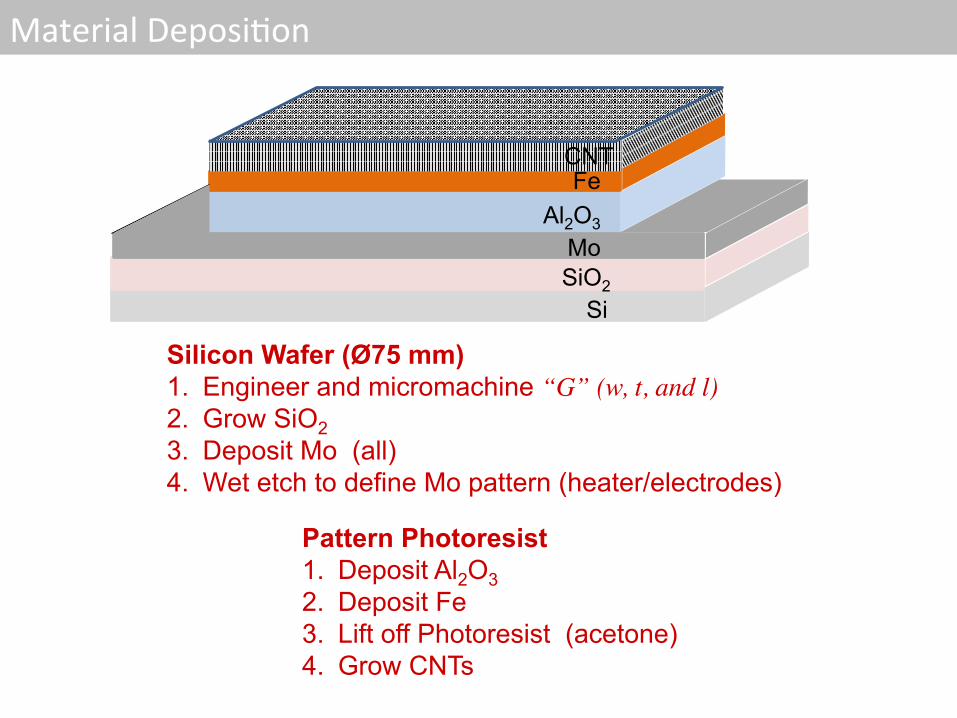
Material DeposiFon
Silicon Wafer (Ø75 mm) 1. Engineer and micromachine “G” (w, t, and l) 2. Grow SiO2 3. Deposit Mo (all) 4. Wet etch to define Mo pattern (heater/electrodes)
Pattern Photoresist 1. Deposit Al2O3 2. Deposit Fe 3. Lift off Photoresist (acetone) 4. Grow CNTs
Si SiO2
Al2O3
CNT
Mo
Fe

Material DeposiFon
75 mm

Carbon nanotube electrical substitution bolometer radiometer Planar electrical-substitution carbon nanotube cryogenic radiometer 6
Figure 10. (a) VACNT at 4K and (b) Mo at 3.884K temporalresponse due to chopping the optical power (⇡102 µW). Thedigitization in (a) is due to the low resolution of the oscilloscope.Shading indicates times when optical power is o↵.
optical power (dark), then 30 µW of electrical powerand 100 µW of optical power (distributed evenly over a1mm diameter circle) is applied (light). For both cases,the modeled power loss due to the eight wirebondsis ⇡ 2 µW, while the power loss due to radiation is⇡ 40 pW. The mean temperature at the thermistor is0.09mK less for the dark case (figure 9c). In order toperfectly match the temperature at the thermistor forboth cases, an additional power of 0.05 µW is neededfor the dark electrical power. We use this modeledpower di↵erence in order to get a correction for thepower inequivalence (�Pequiv).
8. Time constant
To find the time constant of the PBR, we usedthe optical switch to chop the optical power whilemonitoring the current-biased thermistor voltage onan oscilloscope. An exponential fit to the thermistorvoltage signal yielded a time constant (1/e) of 11.8msat 4K (figure 10a).
Due to the elevated Tc of the Mo, we werealso able to regulate the heatsink temperature in thesuperconducting transition, and monitor the current-biased Mo voltage. An exponential fit to the Mo voltagesignal yielded a time constant (1/e) of 7.7ms at 3.884K(figure 10b).
We attribute the slower VACNT thermistor timeconstant to an additional weak thermal link. Thethermistor behaves as if it is not well thermally coupledto the substrate, perhaps because the growth rate of theVACNT over Mo is higher than over SiO2 (figure 11).The transverse VACNT thermal conductance (nanotubeto nanotube) is orders of magnitude lower than the axial
Figure 11. Schematic sectional view of thermistor VACNTshowing VACNT pulled o↵ substrate over SiO2. Thicknesses arenot to scale.
thermal conductance (nanotube to substrate)[17], whichleads to a longer thermistor time constant.
9. Measuring optical fiber power
In order to measure the optical power leaving the fiber,the following steps are performed:(i) Optical switch to port 1 (power meter). (1 s)
(ii) Pause to stabilize power meter. (4 s)
(iii) Record power meter reading. (1 s)
(iv) Pause for temperature stabilization of PID loops.(44 s)
(v) Record dark (optical power o↵) voltages. (2 s)
(vi) Optical switch to port 2 (PBR). (1 s)
(vii) Pause for temperature stabilization of PID loops.(44 s)
(viii) Record light (optical power on) voltages. (2 s)These eight steps, which take a total time of99 s, constitute two independent and traceableoptical fiber power measurements: a PBR electrical-substitution measurement and a commercial powermeter measurement.
PPBR = (1�RTHR)
·✓
Vref,D � Vref,D,0
Rref
◆· (VD � VD,0) + �Pequiv
�✓Vref,L � Vref,L,0
Rref
◆· (VL � VL,0)
�(1)
The measurement equation for the PBR powermeasurement (PPBR) is shown in equation 1. Line 1is a correction for the non-unity VACNT absorption.Line 2 is the Joule power dissipated in the electricalheater with the optical power o↵ (dark), where Rref
is the current reference resistor, Vref,D is the voltageacross Rref with o↵set voltage Vref,D,0, and VD is thevoltage across the Mo heater with o↵set voltage VD,0.The term �Pequiv is the o↵set power correction due tononequivalence determined from the FEM. Line 3 is
Tomlin, et al., Metrologia 52 (2015) 376–383 SPEED

Carbon nanotube electrical substitution bolometer radiometer Planar electrical-substitution carbon nanotube cryogenic radiometer 8
Table 2. Typical uncertainty budget for the opticalpower meter measurement equation (equation 2). Values(uncertainties) shown are the mean value (uncertainty) of 100measurements. For type A uncertainties, N is the number ofmeasurements. When N is not listed, the uncertainty is thecombined uncertainty (k = 1) from a separate measurement.
The last column (percent fractional uncertainty) is | @PPM
@x
·u
x
|/PPM · 100. The expanded uncertainty is k = 2.
uncertainty
variable value (x) type/N value (ux
) % frac.
P1 (µW) 96.3 A/1 0.1 0.12
Cabs 1.0058 A 0.0025 0.25
CNL (P1) 0.99999 A 0.000 65 0.065
upol 1 B 0.000 08 0.008
rswitch 1.059 A/4 0.001 0.1
uf,bend 1 B 0.000 26 0.026
nair 1.0002 B 0.000 001 0.000 02
nf,cold 1.443 10 A 0.000 01 0.0001
nf,warm 1.444 40 A 0.000 01 0.0001
PPM (µW) 101.43
combined uncertainty (µW) 0.31 0.30
expanded uncertainty (µW) 0.62 0.61
9.1. Linearity
As a check of linearity, the eight measurement stepswere performed for 100 di↵erent applied optical powersfrom 10 µW to 460 µW (figure 13). From the FEM,we fit �Pequiv = m · P1 + b where m = 3.4⇥ 10�4 andb = 6.2 nW. A linear fit to the di↵erence of PPM�PPBR
shows that PPM is consistently higher than PPBR by0.09%. While this di↵erence is within the combineduncertainties, it suggests that some of the uncertaintiesmay be biased.
For the linearity measurements, the heatsink wasregulated at 4.0776K and the PBR was regulated at4.8074K (R = 304⌦). The mean of the 99 s standarddeviation (k = 2) temperature fluctuations of theheatsink and PBR temperatures were 1mK and 4mK,respectively.
10. Discussion
The main limitation of the current PBR measurementsis the poor sensitivity of the VACNT thermistor,which leads to poor PID temperature stability. Asa performance test, we swapped the roles of theVACNT thermistor and Mo heater to be VACNTheater and Mo thermistor. Since the Mo transitionis much more sensitive than the VACNT, the PIDtemperature fluctuations of the PBR are 38 times lower.Additionally, the Mo was operated under a current
Figure 13. Results of 100 measurements of varying appliedoptical powers. (a) PPBR has been subtracted purely forfigure clarity and no error propagation was performed for thesubtraction. The expanded uncertainty (k = 2) is shown by errorbars. The solid red line is a linear fit to the P
PM
o↵set with aslope of 0.0009. (b) Fractional uncertainty percentage vs. power.
bias, which is a positive electrothermal feedback mode.The temperature fluctuations would be even lower ifoperated under a voltage bias, which is a negativeelectrothermal feedback mode[22]. However, the PBRwas not designed for operation in this swapped mode,and the poor thermalization of the VACNT heaterleads to measurements of PPBR that are low (2.3%below PPM), which we attribute to blackbody radiationfrom the hot VACNT heater coupling to the VACNTabsorber.
By using a more sensitive voltage-biased Mothermistor and a normal metal heater, the uncertaintyof future PBR measurements should be limited only bythe uncertainty in the measurement of the reflectanceof the VACNT.
In conclusion, we have demonstrated results ofa lithographic electrical-substitution carbon nanotuberadiometer. The lithographic design allows for greaterflexibility and lower time constants, compared totraditional cryogenic radiometers. In addition tobeing a primary standard for optical power, by furtherdecreasing the time constant and using high speed PIDelectronics, the PBR could find applications in Fouriertransform infrared (FTIR) spectroscopy.
Acknowledgments
SEM image was taken by Aric Sanders in the PrecisionImaging Facility at NIST Boulder.
“electrical” “opFcal”
Tomlin, et al., Metrologia 52 (2015) 376–383 EQUIVALENCE

Low-Temperature Nanotube Bolometer Behavior Planar electrical-substitution carbon nanotube cryogenic radiometer 5
Figure 8. (a) Mo heater resistance as a function of temperaturewith logistic function fit R = Rn/ (1 + exp (� (T � Tc) /�T )).Since the transition is not symmetric about Tc, we fit fordi↵erent values of �T below Tc (�T = 8.4mK) and above Tc
(�T = 34.4mK). The dashed vertical line shows Tc. In order toconvert to resistivity, the formula ⇢ = R · 2.5⇥ 10�9 m can beused. (b) Thermistor sensitivity figures of merit, calculated fromfits. At Tc, the Mo TCR = 14.1K�1 and ↵ = 54.9.
shows two common thermistor sensitivity figures ofmerit, temperature coe�cient of resistance (TCR =1/R · dR/dT ) and ↵ = T/R · dR/dT .
6. Heater
Due to an unexpected elevation of the Mo superconduct-ing critical temperature (Tc) to 3.884K (figure 8a), weare limited to operating temperatures above Tc wherethe Mo is normal (Rn = 74.5⌦) and the electrical heaterdissipates heat. Since Mo usually has a Tc below 1K,we speculate that the VACNT growth modifies the Mo,possibly forming molybdenum carbide. On separatedevices, we have measured Tc values up to 7K. Theelevated Tc opens the possibility for future devices touse the Mo as an extremely sensitive thermistor (fig-ure 8b) operating as a transition-edge sensor (TES).Additionally, Mo traces could be used for thin-filmsuperconducting wiring instead of Al wirebonds.
7. Thermal modeling
By varying the applied electrical power (Pelec) from1 µW to 800 µW and monitoring the thermistortemperature, we find that the thermal conductance ofthe PBR is best fit by a cubic temperature dependenceof G = dPelec/dT = G0T
3, where G0 is a constant. Theintegrated power law is then Pelec = G0/4
�T
4 � T
4HS
�,
where THS is the temperature of the heatsink. Solvingfor G0 and using measured values of Pelec = 131.15 µW,T = 4.325K, and THS = 4.0772K gives G0 =
Figure 9. (a) Modeled 2D FEM temperature profile for 130 µWof applied power. Color legend not shown, see part (b) fortemperatures. (b) 1D temperature profile along center of 2DFEM (part (a)) for two cases (dark and light) described in text.(c) Di↵erence in temperature of two curves in part (b).
7.13 µWK�4. This gives a thermal conductance at4K of 456 µWK�1.
Using finite-element model (FEM) software, wehave modeled the two dimensional (2D) temperatureprofile of the PBR. We have assumed the Si thermalconductivity is isotropic with a temperature dependenceof Si = Si,0T
3, where Si,0 is an unknown constant.For the conductivity of the Al wirebonds, we haveassumed a linear temperature dependence of Al =Al,0T with Al,0 = 3Wm�1 K�2[15]. Therefore,the power loss due to one Al wirebond is PAl,1 =1/2 (Al/T ·AAl/LAl)
�T
2 � T
2HS
�, where AAl is the
wirebond cross sectional area and LAl is the wirebondlength. The power loss due to blackbody radiation isPrad = A�✏
�T
4 � T
4HS
�, where A is the area, � is the
Stefan-Boltzmann constant, and ✏ is the emissivity with✏VACNT = 1 and ✏Si = 0.1[5, 16]. The model required avalue of Si,0 = 0.166Wm�1 K�4 in order to match themeasured conditions of Pelec, T , and THS listed above.
Figure 9a shows the modeled 2D FEM temperatureprofile for an applied power of 130 µW. Two crosssection temperature profiles are shown in figure 9b,which simulate an electrical substitution measurement.First, 130 µW of electrical power is applied without any
SuperconducFng TransiFon Near 4 K
Tomlin, et al., Metrologia 52 (2015) 376–383 SENSITIVITY

Carbon Nanotube Base Detectors
Broad, efficient and uniform wavelength range visible to 500 micrometers (!?) (BRDF needed)

τ ~ 1 ms
Carbon Nanotube Base Detectors
Fast (suitable for FTIR)
Broad, efficient and uniform wavelength range visible to 500 micrometers (!?) (BRDF needed)

τ ~ 1 ms
Carbon Nanotube Base Detectors
Fast (suitable for FTIR)
Scalable, reproducible Optimize per application fiber, space, few photon (open mind required)
Broad, efficient and uniform wavelength range visible to 500 micrometers (!?) (BRDF needed)

NIST-Gaithersburg (MIR/speed)
PTB Berlin (THz/FIR)
GREYC / Univ. Caen (speed) NIST-Boulder (optical fiber)
NIST Nanotube Bolometer Workshop, July 22, 23, 24, 2015 Boulder, Colorado, USA hmp://www.nist.gov/pml/div686/nanotube-‐bolometer-‐workshop.cfm