Embed Size (px)
Citation preview

2.4G ~ 10.4G Hz CMOS programmable Frequency Divider
Kang, Shi-Yun
Wen, Hsiang-Chih
LiTH-ISY-EX--05/3750--SE

2.4G ~ 10.4G Hz CMOS
programmable Frequency Divider
Computer Engineering Department of Electrical Engineering (ISY)
Linköpings University
Kang, Shi-Yun
Wen, Hsiang-Chih LiTH-ISY-EX--05/3750--SE
Examiner
Dake Liu, ISY, LiTH, Sweden Supervisor
Gin-Kou Ma, STC, ITRI, Taiwan


Avdelning, Institution Division, Department Institutionen för systemteknik 581 83 LINKÖPING
Datum Date 2005-05-09
Språk Language
Rapporttyp Report category
ISBN
Svenska/Swedish X Engelska/English
Licentiatavhandling X Examensarbete
ISRN LITH-ISY-EX-3750-2005
C-uppsats D-uppsats
Serietitel och serienummer Title of series, numbering
Övrig rapport ____
ISSN -
URL för elektronisk version http://www.ep.liu.se/exjobb/isy/2005/3750/
Titel Title
2.4G ~ 10.4G Hz CMOS programmable Frequency Divider
Författare Author
Kang, Shi-Yun Wen, Hsiang-Chih
Sammanfattning Abstract This master thesis is as a final project in the Division of Computer Engineering at the Department of Electrical Engineering, Linköpings University, Sweden. The purpose of the project is to design a wide frequency range programmable frequency divider used in a PLL circuit for ultra wide band system. 0.18 um tsmc CMOS technology is used in this project. A brief introduction of PLL circuits and UWB specifications are given in the report and the circuit design issue is presented. Post-layout simulation results are shown in the later part of the report. The focus of this project is to make the frequency divider work well in wide range and high speed. Therefore, how to shorten feedback circuits’ latency and how to reduce complexity of the circuits are the main problems. Logic gate merged technique is used to reduce transistor number and carefully drawing layout makes the circuit work well in post-layout simulation.
Nyckelord Keyword frequency divider, ultra wideband


ABSTRACT ________________________________________________________________________
Abstract This master thesis is as a final project in the Division of Computer Engineering at
the Department of Electrical Engineering, Linköpings University, Sweden.
The purpose of the project is to design a wide frequency range programmable
frequency divider used in a PLL circuit for ultra wide band system. 0.18 um tsmc CMOS
technology is used in this project.
A brief introduction of PLL circuits and UWB specifications are given in the report
and the circuit design issue is presented. Post-layout simulation results are shown in the
later part of the report.
The focus of this project is to make the frequency divider work well in wide range
and high speed. Therefore, how to shorten feedback circuits’ latency and how to reduce
complexity of the circuits are the main problems. Logic gate merged technique is used to
reduce transistor number and carefully drawing layout makes the circuit work well in
post-layout simulation.


ACKNOWLEDGMENT ________________________________________________________________________
Acknowledgment We would like to thank SoC Technology Center of ITRI (Industrial Technology
Research Institute) in Taiwan. They provide us good research environment and give us
good suggestion about our work.
We would like to thank Dr. Gin-Kou Ma, Director of Mixed Signal Design
Technologies Division of STC/ITRI, for offering us this opportunity to work on this
project.
We would like to thank Dake Liu, Professor and the chair of Computer Engineering
Division in Linköpings University. He gives us good suggestions about project time plan
and always encourages and supports us during these months.
We would like to thank Po-Chiun Huang, assistant professor in department of
electrical engineering in National Tsing-Hua University in Taiwan, for giving us good
and useful suggestion about project topic selection.

TABLE OF CONTENT ________________________________________________________________________
Table of Content Chapter 1 Introduction
1.1 Chapter overview..................................................................................................1
1.2 Introduction...........................................................................................................1
1.3 Focus and motivations of the thesis......................................................................2
1.4 Organization of the thesis......................................................................................2
Chapter 2 Phase-Locked Loop 2.1 Chapter overview..................................................................................................3
2.2 PLL basics.............................................................................................................3
2.3 PLL Synthesizer Basic Building Blocks...............................................................7
2.3.1 Phase-Frequency Detector (PFD)..............................................................8
2.3.2 Charge-Pump (CP) and loop filter...........................................................11
2.3.3 Voltage-Controlled Oscillator (VCO)......................................................12
2.3.4 Frequency divider....................................................................................13
2.4 Summary ............................................................................................................14
Chapter 3 Ultra wideband 3.1 Chapter overview................................................................................................15
3.2 Introduction to ultra wideband............................................................................15
3.3 Operating frequency range..................................................................................16
3.4 Summary.............................................................................................................18
Chapter 4 Frequency divider 4.1 Chapter overview................................................................................................19
4.2 Publications on CMOS frequency divider...........................................................19
4.3 Block diagram and block description..................................................................20
4.4 Design circuit description....................................................................................22
4.4.1 div8_9......................................................................................................23
4.4.2 3Bcounter.................................................................................................30
4.4.3 5Bcounter.................................................................................................34
4.5 Summary.............................................................................................................35

TABLE OF CONTENT ________________________________________________________________________
Chapter 5 Simulation 5.1 Chapter overview................................................................................................37
5.2 Simulation – UWB system requirement..............................................................37
5.3 Simulation – reset divide ratio.............................................................................45
5.4 Simulation – robustness.......................................................................................46
5.5 Simulation – working range................................................................................47
5.6 Layout..................................................................................................................48
Chapter 6 Conclusion 6.1 Conclusion...........................................................................................................49
6.2 Problems encountered.........................................................................................49
6.3 Future improvements...........................................................................................49
Reference.......................................................................................................................51

INTRODUCTION ________________________________________________________________________
Chapter 1 Introduction 1.1 Chapter overview
This chapter explains the focus of this thesis and the motivation behind this work.
Further, it provides the thesis organization.
1.2 Introduction
Phase-Locked Loops (PLLs) are functional circuits that generate signals
phase-locked with external input signals. They are widely used for synchronization
purposes and are essential in communication field.
Owing to the broad use of mobile electronic systems, low-power consumption and
low jitter have become the main concern in PLLs design. Besides, fast lock time is
required in nearly all PLL applications.
PLLs are generally built of a phase frequency detector, a charge pump, a low pass
filter, a level shifter, a voltage-controlled oscillator, and a frequency divider in the
feedback path.
Due to the high operation frequency of the frequency dividers, they usually
consume much more power than the other components in PLLs.
RF design has traditionally been done in Bipolar or Gallium Arsenide (GaAs)
technologies and SiGe-Bipolar process is also gaining widespread acceptance.
Complementary-Metal-Oxide-Semiconductor (CMOS) technology is a cheaper
alternative to other commercially available IC fabrication processes. There is a growing
financial incentive to develop single-chip transceivers, high-speed microprocessors, fiber
optic sub-systems and complex Systems-On-Chip (SoC) using CMOS technology.
CMOS is an area of active research driven primarily by the wireless market. CMOS is the
technology of choice for consumer electronics, microprocessors, networking, memories
and video clock generators because of its very low power dissipation and cost.
1

INTRODUCTION ________________________________________________________________________
1.3 Focus and motivations of the thesis
Ultra wideband (UWB) is a unique and new usage of a recently legalized frequency
spectrum. We found that there is no previous work about frequency divider can fit UWB
system. (UWB system will be further discussed in chapter three.)
Therefore, the focus of this thesis is to design a CMOS programmable
dual-modulus frequency divider of a PLL for Ultra wideband system.
In order to be used in transceivers for UWB system. The divider should accept
input frequency from 3G to 10G Hz. Besides, the frequency divider should be able to
change divide ratio in a short time. In section 5.2 and 5.3, we have some discussion about
specification of a frequency divider for UWB system and show that our design can fit the
specification.
1.4 Organization of the thesis
There are six chapters in the thesis. These are organized as follows:
Chapter 2 mentions the PLL-FS concepts and introduces each block’s function and
basic circuit of PLL.
Chapter 3 introduces Ultra wideband system. Give a roughly idea about its basic
technology and band allocation.
Chapter 4 presents the circuit design of the components in programmable frequency
divider.
Chapter 5 presents the simulation results for the programmable frequency divider.
Chapter 6 outlines the conclusions drawn from this work and proposes some future
research possibilities.
References cited are listed at the end of this thesis document
2

PHASE-LOCKED LOOP ________________________________________________________________________
Chapter 2 Phase-Locked Loop 2.1 Chapter overview
This chapter briefly introduces the concepts of the PLLs. First, the basic principle
of operation and PLL architecture is described. Then, a detailed description of each
blocks of the PLL synthesizer is given.
2.2 PLL basics
A phase-locked loop is a feedback system combining a voltage controlled oscillator
and a phase comparator which can make the oscillator frequency (or phase) accurately
tracks that of an applied frequency- or phase-modulated signal. Phase-locked loops can
be used to generate stable output frequency signals from a fixed low-frequency signal.
The first phase-locked loops were implemented in the early 1930s by a French engineer,
de Bellescize. However, they only found broad acceptance in the market place when
integrated PLLs became available as relatively low-cost components in the mid-1960s.
The phase locked loop can be analyzed in general as a negative feedback system with a
forward gain term and a feedback term. A simple block diagram of a voltage-based
negative-feedback system is shown in Figure 2.1
Figure 2.1 Standard negative-feedback control system model
3
PHASE-LOCKED LOOP ________________________________________________________________________
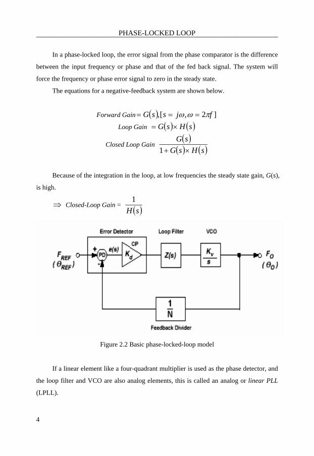
In a phase-locked loop, the error signal from the phase comparator is the difference
between the input frequency or phase and that of the fed back signal. The system will
force the frequency or phase error signal to zero in the steady state.
The equations for a negative-feedback system are shown below.
Forward Gain ( ) ]2,[, fjssG πωω ===
Loop Gain ( ) ( )sHsG ×=
Closed Loop Gain ( )
( ) ( )sHsGsG×+1
Because of the integration in the loop, at low frequencies the steady state gain, G(s),
is high.
⇒ Closed-Loop Gain = ( )sH1
Figure 2.2 Basic phase-locked-loop model
If a linear element like a four-quadrant multiplier is used as the phase detector, and
the loop filter and VCO are also analog elements, this is called an analog or linear PLL
(LPLL).
4
PHASE-LOCKED LOOP ________________________________________________________________________
If a digital phase detector (EXOR gate or J-K flip flop) is used, and everything else
stays the same, the system is called a digital PLL (DPLL).
If the PLL is built exclusively from digital blocks, without any passive components
or linear elements, it becomes an all-digital PLL (ADPLL).
With information in digital form, and the availability of sufficiently fast processing,
it is also possible to develop PLLs in the software domain. The PLL function is
performed by software and runs on a DSP. This is called a software PLL (SPLL).
Referring to Figure 2.2, a system for using a PLL to generate higher frequencies
than the input, the VCO oscillates at an angular frequency of WD. A portion of this
frequency/phase signal is fed back to the error detector, via a frequency divider with a
ratio 1/N. This divided-down frequency is fed to one input of the error detector. The other
input in this example is a fixed reference frequency/phase. The error detector compares
the signals at both inputs. When the two signal inputs are equal in phase and frequency,
the error will be zero and the loop is said to be in a “locked” condition. If we simply look
at the error signal, the following equations may be developed.
( )NFoFrefse −=
When
( )
FrefNFo
se
=⇒
= 0
Thus
FrefNFo ×=
In commercial PLLs, the phase detector and charge pump together form the error
detector block. When FrefNFo ×≠ , the error detector will output source/sink current
pulses to the low pass loop filter. This transfers the current pulses into a voltage which in
turn drives the VCO. The VCO frequency will then increase or decrease as necessary,
by , where is the VCO sensitivity in MHz/Volt and VKv∆ Kv V∆ is the change in
VCO input voltage. This will continue until e(s) is zero and the loop is locked. The
5
PHASE-LOCKED LOOP ________________________________________________________________________
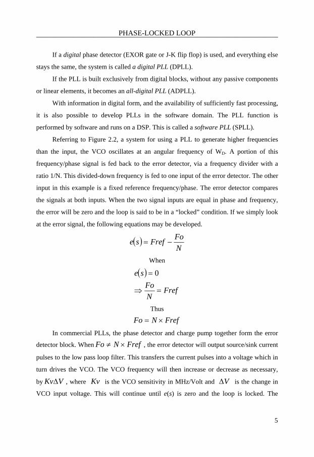
charge pump and VCO thus serves as an integrator, seeking to increase or decrease its
output frequency to the value required so as to restore its input (from the phase detector)
to zero.
Figure 2.3 VCO transfer function
The overall transfer function (Closed-Loop Gain) of the PLL can be expressed
simply by using the Closed-Loop Gain expression for a negative feedback system as
given above.
( )
( )Ns
sKvZKHGLoopGain
ssKvZKGnForwardGai
LoopGainnForwardGai
FrefFo
D
D
=×
=
+=
,
,
1
When GH is much greater than 1, we can say that the closed loop transfer function
for the PLL system is N and so
FrefNFo ×=
6

PHASE-LOCKED LOOP ________________________________________________________________________
The loop filter is a low-pass type, typically with one pole and one zero. The
transient response of the loop depends on:
1. the magnitude of the pole/zero,
2. the charge pump magnitude,
3. the VCO sensitivity,
4. the feedback factor, N.
All of the above must be taken into account when designing the loop filter. In addition,
the filter must be designed to be stable (usually a phase margin of p/4 is recommended).
The 3-dB cutoff frequency of the response is usually called the loop bandwidth, BW.
Large loop bandwidths result in very fast transient response. However, this is not always
advantageous, since there is a tradeoff between fast transient response and reference spur
attenuation.
2.3 PLL Synthesizer Basic Building Blocks
A PLL synthesizer can be considered in terms of several basic building blocks.
Figure 2.4 Charge-pump PLL block diagram
7
PHASE-LOCKED LOOP ________________________________________________________________________
• Phase-Frequency Detector (PFD)
• Charge-Pump (CP)
• Low-Pass Filter (LPF)
• Voltage-Controlled Oscillator (VCO)
• VCO Level-Shifter (LS)
• Frequency Divider
2.3.1 Phase-Frequency Detector (PFD)
This is where the reference frequency signal is compared with the signal fed back
from the VCO output, and the resulting error signal is used to drive the loop filter and
VCO. In a digital PLL (DPLL) the phase detector or phase-frequency detector is a logical
element. The three most common implementations are:
Exclusive-or (EXOR) Gate
J-K Flip-Flop
Digital Phase-Frequency Detector
Figure 2.5 shows one implementation of a PFD, basically consisting of two D-type flip
flops. One Q output enables a positive current source; and the other Q output enables a
negative current source. Assuming that, in this design, the D-type flip flop is
positive-edge triggered, the states are these (Q1, Q2):
11—both outputs high, is disabled by the AND gate (U3) back to the CLR pins on the
flip flops.
00—both P1 and N1 are turned off and the output, OUT, is essentially in a high
impedance state.
10—P1 is turned on, N1 is turned off, and the output is at V+.
01—P1 is turned off, N1 is turned on, and the output is at V–.
8

PHASE-LOCKED LOOP ________________________________________________________________________
Figure 2.5 Typical PFD using D-type flip flops
onsider now how the circuit behaves if the system is out of lock and the frequency at C
+IN is much higher than the frequency at –IN, as exemplified in Figure 2.6.
Figure 2.6 PFD waveforms, out of frequency and phase lock
Since the frequency at +IN is much higher than that at –IN, the output spends most
of its time in the high state. The first rising edge on +IN sends the output high and this is
maintained until the first rising edge occurs on –IN. In a practical system this means that
9

PHASE-LOCKED LOOP ________________________________________________________________________
the output, and thus the input to the VCO, is driven higher, resulting in an increase in
frequency at –IN. This is exactly what is desired.
If the frequency on +IN were much lower than on –IN, the opposite effect would
occur. The output at OUT would spend most of its time in the low condition. This would
have the effect of driving the VCO in the negative direction and again bring the
frequency at –IN much closer to that at +IN, to approach the locked condition. Figure 2.7
shows the waveforms when the inputs are frequency-locked and close to phase-lock.
Figure 2.7 PFD waveforms, in frequency lock but out of phase lock
Since +IN is leading –IN, the output is a series of positive current pulses. These
pulse
t of this cycling would be for the
outpu
s will tend to drive the VCO so that the –IN signal become phase-aligned with that
on +IN. When this occurs, if there were no delay element between U3 and the CLR
inputs of U1 and U2, it would be possible for the output to be in high-impedance mode,
producing neither positive nor negative current pulses. This would not be a good situation.
The VCO would drift until a significant phase error developed and started producing
either positive or negative current pulses once again.
Over a relatively long period of time, the effec
t of the charge pump to be modulated by a signal that is a sub harmonic of the PFD
input reference frequency. Since this could be a low frequency signal, it would not be
attenuated by the loop filter and would result in very significant spurs in the VCO output
spectrum, a phenomenon known as the backlash effect. The delay element between the
output of U3 and the CLR inputs of U1 and U2 ensures that it does not happen. With the
delay element, even when the +IN and –IN are perfectly phase-aligned, there will still be
10

PHASE-LOCKED LOOP ________________________________________________________________________
a current pulse generated at the charge pump output. The duration of this delay is equal to
the delay inserted at the output of U3 and is known as the anti-backlash pulse width.
2.3.2 harge-Pump (CP) and loop filter C
Figure 2.8 Charge pump and loop filter
Charge pump and loop filter provide a way to avoid some of the unpleasantness of
p and loop filter network. The phase
detector meters voltage sources UP and DOWN pulses
the available resistors and capacitors in CMOS.
In figure 2.8, it is a 4 input charge pum
( DDUU ,,, ). UP pulses cause
REF pulses rem
nce onto the control
ltag
I to add charge to the loop filter capacitor, whereas DOWN ove charge. The
discrete resistor R supplies the “zero” needed to stabilize the loop.
At lock, the charge pump will introduce synchronous disturba
vo e arising from mismatches between the UP and DOWN pulling current sources,
mismatches in the switching waveforms and in the switch devices themselves and charge
11

PHASE-LOCKED LOOP ________________________________________________________________________
injection from parasitic capacitances in the current sources. The loop filter cannot remove
all of the ripples because of the resistor R that provides the stabilizing zero in the loop
transfer function and thus the ripple will modulate the VCO and produce jitter on its
output.
2.3.3 oltage-Controlled Oscillator (VCO)
VCO, which takes a control input Vc, and
Where fc is the center equency of the VCO and Kv is the gain. The gain determines
VCO. One is ring oscillators and
e ot
ring of an odd number of inverters. The frequency is
ried
g a
ltag
V
The key component of the phase-lock loop is a
produces a periodic signal with frequency
KvVcfcf +=
fr
frequency range and stability. The larger the gain, the larger the frequency range for a
given range of Vc. However, a large gain also makes the VCO more susceptible to noise
on Vc, giving a less stable frequency source. In general the VCO is designed with the
smallest gain that gives the required frequency range.
Two type circuits are in common used to design a
th her is resonant oscillators.
A ring oscillator VCO is a
va by either changing the number of stages, the delay of each stage, or both. Often a
digital coarse adjustment selects the number of stages and an analog fine adjustment
determines the delay per stage. Ring oscillator VCOs are very popular on integrated
circuits because they can be built without the external inductors, crystals required for
resonant VCOs. However, they usually give a noisier clock than a resonant oscillator.
A resonant VCO uses an LC or crystal oscillator and tunes the frequency usin
vo e-variable capacitor. Voltage-controlled crystal oscillators typically have a very
narrow frequency range and provide a very stable clock source. For applications where a
narrow frequency range is adequate and phase noise is an issue, a resonant VCO is
usually preferred.
12

PHASE-LOCKED LOOP ________________________________________________________________________
2.3.4 Frequency divider
runs at the same frequency as the VCO, the design of this
circui
grammable dual modulus divider includes an N/N+1 prescaler and two
ogr
Because the divider
t is difficult and often determines the maximum usable frequency of the PLL
synthesizer. The choice of the divider architecture is essential for achieving low-power
dissipation, high design flexibility of existing building blocks. Usually, the first or first
few stages of the divider are fixed frequency divider, called prescaler. The rest of the
divider is programmable and often based on a variant of dual modulus division
techniques.
A pro
pr ammable down counters (N1counter, N2counter).The dividers works as follows.
Figure 2.9 Programmable frequency divider
The count output signals of both counters are low as long as the counter has not
counted down zero. The divide ratio of prescaler is N+1. When N2counter counts down
to zero, it remains at zero and wait for N1counter to reach zero. The divide ratio of
precaler will be changed to N. Once N1counter reaches zero, the circuit reloads both
counters with their programmed values. The divide ratio of prescaler will change back to
13

PHASE-LOCKED LOOP ________________________________________________________________________
N+1. A constraint in the two programmed input values is that Nlcounter value must
always be greater than N2counter value.
Assuming that N1counter and N2counter are initially loaded with their
progr
N2 + (N1-N2)×N = N1×N + N2 --- (1)
After counting N1× r are automatically
2.4 Summary
apter, we have introduced the basic concepts of PLLs with simple block
diagr
ammed values, the prescaler is dividing by N+1 until N2counter counts down to
zero. Then, from that moment, the prescaler will divide by N until N1counter reaches
zero. The total number of input cycles counted by N2counter is (N+1)×N2 and that of
N1counter is (N1-N2). Therefore, the whole dual-modulus divider block performs the
operation described below:
(N+1)×
N+N2 input cycles, N1counter and N2counte
reloaded with the programmed inputs and the whole cycle repeats. Based on Equation (1),
the circuit divides the input frequency by N1×N + N2. To have a continuous division
ratios from 56 to 255, the values programmed into the dual-modulus divider are N = 8,
N1COUNTER = 31 to 7 I, and N2COUNTER = 7 to 0. Based on the requirement for
N1counter, N2counter and N values, where N is the frequency divider input, N1counter
circuit must have a minimum of 5-bit control input, and a 3-bit control input for
N2counter. The frequency divider, on the other hand, divides by 8 or 9, depending on the
modulus control input.
In this ch
ams and equations and discussed the main architecture of PLL’s each block.
14

ULTRA WIDEBAND ________________________________________________________________________
Chapter 3 Ultra wideband 3.1 Chapter overview
This chapter will give an introduction of Ultra wideband (UWB) system. How
UWB work, basic technology of UWB, advantages of UWB and the band allocation of
UWB will be briefly described.
3.2 Introduction to ultra wideband
UWB is a unique and new usage of a recently legalized frequency spectrum. UWB
radios can use frequencies from 3.1 GHz to 10.6 GHz—a band more than 7 GHz wide.
Each radio channel can have a bandwidth of more than 500 MHz, depending on its center
frequency. To allow for such a large signal bandwidth, the Federal Communications
Commission (FCC) put in place severe broadcast power restrictions. By doing so, UWB
devices can make use of an extremely wide frequency band while not emitting enough
energy to be noticed by narrower band devices nearby, such as 802.11a/g radios. This
sharing of spectrum allows devices to obtain very high data throughput, but they must be
within close proximity.
Strict power limits mean the radios themselves must be low power consumers.
Because of the low power requirements, it is feasible to develop cost-effective CMOS
implementations of UWB radios. With the characteristics of low power, low cost, and
very high data rates at limited range, UWB is positioned to address the market for a
high-speed Wireless Personal Area Networks (WPANs).
UWB technology also allows spectrum reuse. A cluster of devices in proximity (for
example, an entertainment system in a living area) can communicate on the same channel
as another cluster of devices in another room (for example, a gaming system in a
bedroom). UWB-based WPANs have such a short range that nearby clusters can use the
same channel without causing interference.
An 802.11g WLAN solution, however, would quickly use up the available data
bandwidth in a single device cluster, and that radio channel would be unavailable for
15
ULTRA WIDEBAND ________________________________________________________________________
reuse anywhere else in the home. Because of UWB technology’s limited range, 802.11
WLAN solutions are an excellent complement to a WPAN, serving as a backbone for
data transmission between home clusters.
3.3 Operating frequency range
UWB systems use some specific modulation techniques, such as Orthogonal
Frequency Division Multiplexing (OFDM), to occupy these extremely wide bandwidths.
OFDM distributes the data over a large number of carriers that are spaced apart at precise
frequencies. This spacing provides the orthogonality in this technique, which prevents the
demodulators from seeing frequencies other than their own. The benefits of OFDM are
high-spectral efficiency, resiliency to RF interference, and lower multipath distortion.
By using OFDM modulation techniques coupled with multibanding, it becomes
easier to collect multipath energy using a single RF chain and allows the receiver to deal
with narrowband interference without having to sacrifice subbands or data rate. These
advantages relate to the ability to turn off individual tones and also easily recover
damaged tones through the use of forward error-correction coding.
The MultiBand OFDM approach allows for good coexistence with narrowband
systems such as 802.11a, adaptation to different regulatory environments, future
scalability and backward compatibility. This design allows the technology to comply with
local regulations by dynamically turning off subbands and individual OFDM tones to
comply with local rules of operation on allocated spectrum.
In the MultiBand OFDM approach, the available spectrum of 7.5 GHz is divided
into several 528-MHz bands.
The relationship between center frequency and band number is given by the
following equation:
Band center frequency = 2904 + 528n (MHz) n = 1, 2…, 13.
16
ULTRA WIDEBAND ________________________________________________________________________
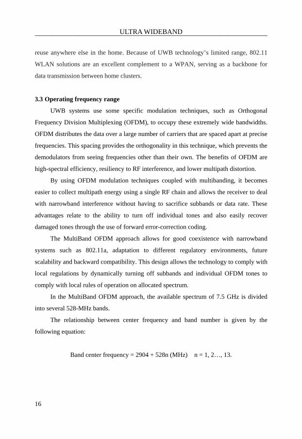
BAND_ID Lower frequency Center frequency Upper frequency
1 3168 MHz 3432 MHz 3696 MHz
2 3696 MHz 3960 MHz 4224 MHz
3 4224 MHz 4488 MHz 4752 MHz
4 4752 MHz 5016 MHz 5280 MHz
5 5280 MHz 5544 MHz 5808 MHz
6 5808 MHz 6072 MHz 6336 MHz
7 6336 MHz 6600 MHz 6864 MHz
8 6864 MHz 7128 MHz 7392 MHz
9 7392 MHz 7656 MHz 7920 MHz
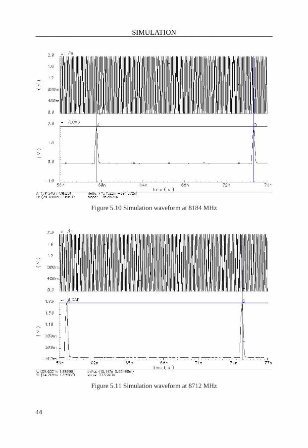
10 7920 MHz 8184 MHz 8448 MHz
11 8448 MHz 8712 MHz 8976 MHz
12 8976 MHz 9240 MHz 9504 MHz
13 9504 MHz 9768 MHz 10032 MHz
Table 3.1 OFDM PHY band allocation
Figure 3.1 Multiband OFDM band allocation
17
ULTRA WIDEBAND ________________________________________________________________________
3.4 Summary
Ultra Wideband is an innovative wireless technology which can transmit digital
data over a wide frequency spectrum with very low power and at very high data rates. As
well as having the ability to transfer high-speed data using low power, Ultra Wideband
can carry signals through many obstacles that usually reflect signals at more limited
bandwidths and at higher power. In addition to the high data rate capability of Ultra
Wideband, its low transmit power also means it transmits negligible interference to
existing systems. The low power properties of ultra wideband communications can allow
systems to operate across a range of frequency bands unlicensed. The power is so low in
fact, that it is below the levels associated with the emission limits for unintentional
transmitters such as televisions and washing machines
18

FREQUENCY DIVIDER ________________________________________________________________________
Chapter 4 Frequency divider 4.1 Chapter overview
This chapter will show our design. In the first section, a survey of the literature on
CMOS frequency divider is given. Then, each blocks of our frequency divider will be
described in detail.
4.2 Publications on CMOS frequency divider
Table 4.1 lists the frequently quoted performance-metrics of CMOS frequency
divider published since 1996. Further, it highlights the focal point of the particular
research.
Year /
Ref.
CMOS
process
fmax at VDD Power Divide
ratio
Advantage / Disadvantage
1996
[1]
0.8 um 1.22GHz at
5 V
25.5mW at
1.22GHz
128/129 Use ratio logic idea to gain high
speed
More static power consumption
1996
[2]
0.7 um 1.75GHz at
3V
24mW at
1.75GHz
128/129 Phase switching technique
lowering slope to prevent spikes
=> lower speed
1998
[3]
0.8 um 1.80GHz at
5V
52.9mW at
1.80GHz
128/129 Modified TSPC
Merge AND+DFF
Consume too much power
1999
[4]
0.8 um 1.36GHz at
3V
9.7m W at
1.3V
128/129 Dynamic-Pseudo NMOS latch
Lower power consumption than
[1]
1999
[5]
0.5 um 1.5GHz at
2.7V
1.7mW at
1.5GHz
16/17 Improve [2], low power.
switch phase from 4 -> 3 =>
easier to balance delay between
19

FREQUENCY DIVIDER ________________________________________________________________________
different path
use SFF(synchronous flip flop)
to prevent spike
2000
[6]
0.25 um 5.5GHz at
2.2V
59mW at
5.5GHz
220~224 Improve [2], higher speed
Use pseudo NMOS divide by
two stage, high speed, high
power
Add a retimer to prevent spike
2003
[7]
0.25 um 2.32GHz at
2.5V
12mW at
2.3GHz
128/129 Improve [2], .simple circuit
May induce spike
2004
[8]
0.25 um 5 GHz at
2.5V
6.25m W at
5 GHz
257~287 Merge AND+DFF / OR+DFF
Lower power
Modified TSPC
2000
[9]
0.35 um 0.57 GHz/m
W
Programmable
Big programmable range
2002
[10]
0.18 um 2.4 GHz at
1.8V
2.3m W at
2.4 GHz
N1N+N2 programmable
low power
2004
[11]
0.18 um 10.4 GHz at
1.8V
28.8m W at
10.4 GHz
256/257 High Speed
range 8.2GHz ~14GHz
Table 4.1
The major conclusion that can be drawn from this literature survey is that the high
speed and programmability are become important. However, in previous works, there is
no frequency divider can be applied to ultra wide band system. Since ultra wideband
system is an innovative wireless technology, we would like to design a frequency divider
which can work from 3G Hz to 10G Hz for UWB system.
4.3 Block diagram and block description
As we mention in chapter two, a programmable dual modulus divider includes an
20
FREQUENCY DIVIDER ________________________________________________________________________
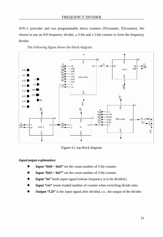
N/N+1 prescaler and two programmable down counters (N1counter, N2counter). We
choose to use an 8/9 frequency divider, a 5-bit and a 3-bit counter to form the frequency
divider.
The following figure shows the block diagram.
Figure 4.1 top block diagram
Input/output explanation:
Input “bit0 ~ bit4” set the count number of 5-bit counter.
Input “bit5 ~ bit7” set the count number of 3-bit counter.
Input “in” feeds input signal (whose frequency is to be divided.)
Input “rst” resets loaded number of counter when switching divide ratio.
Output “LD” is the input signal after divided, i.e., the output of the divider.
21
FREQUENCY DIVIDER ________________________________________________________________________
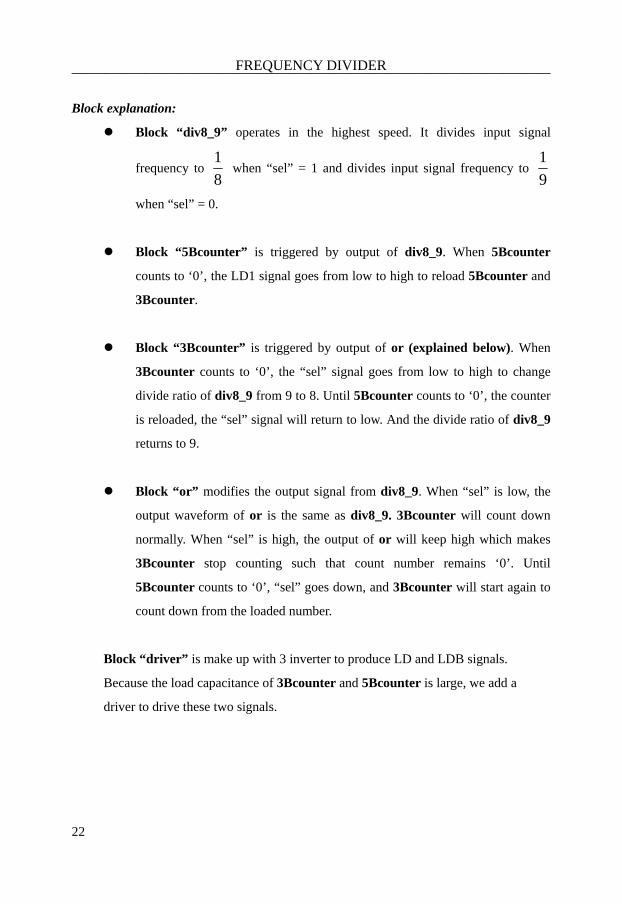
Block explanation:
Block “div8_9” operates in the highest speed. It divides input signal
frequency to 81
when “sel” = 1 and divides input signal frequency to 91
when “sel” = 0.
Block “5Bcounter” is triggered by output of div8_9. When 5Bcounter
counts to ‘0’, the LD1 signal goes from low to high to reload 5Bcounter and
3Bcounter.
Block “3Bcounter” is triggered by output of or (explained below). When
3Bcounter counts to ‘0’, the “sel” signal goes from low to high to change
divide ratio of div8_9 from 9 to 8. Until 5Bcounter counts to ‘0’, the counter
is reloaded, the “sel” signal will return to low. And the divide ratio of div8_9
returns to 9.
Block “or” modifies the output signal from div8_9. When “sel” is low, the
output waveform of or is the same as div8_9. 3Bcounter will count down
normally. When “sel” is high, the output of or will keep high which makes
3Bcounter stop counting such that count number remains ‘0’. Until
5Bcounter counts to ‘0’, “sel” goes down, and 3Bcounter will start again to
count down from the loaded number.
Block “driver” is make up with 3 inverter to produce LD and LDB signals.
Because the load capacitance of 3Bcounter and 5Bcounter is large, we add a
driver to drive these two signals.
22

FREQUENCY DIVIDER ________________________________________________________________________
4.4 Design circuit description
This section provides each block’s circuit implementation.
4.4.1 div8_9
This block is made up with 4 modified TSPC_DFFs and can be separated into two
parts, a 4/5 divider and a DFF.
Figure 4.2 Block diagram of div8_9
Figure 4.3 Modified TSPC_DFF
23
FREQUENCY DIVIDER ________________________________________________________________________
Let’s first look into 4/5 divider. The initial circuit of 4/5 divider is shown below.
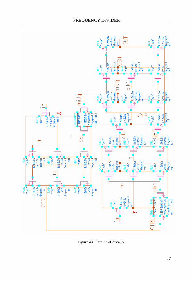
Figure 4.4 Block diagram of div4_5
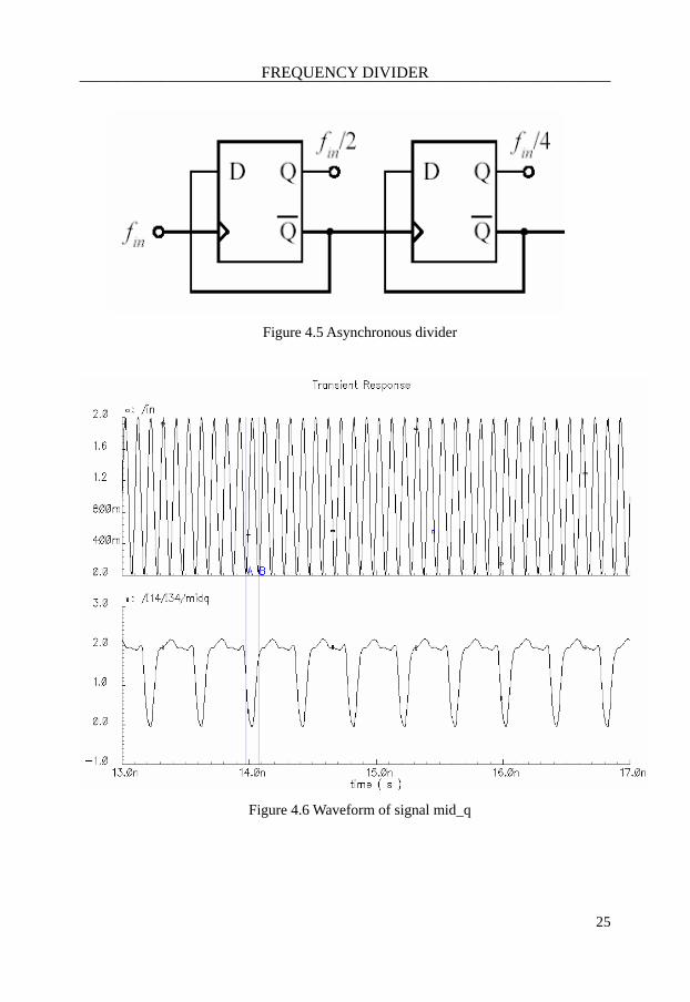
DFF_1 and DFF_2 form an asynchronous divider. When we just use these two DFFs
to make up a divider (figure 4.5), we found that the waveform of signal “mid_q” is a low
voltage pulse with one input signal cycle width and repeat every four cycle (see figure
4.6). We inverse and delay this signal one cycle and then ‘or’ this delay signal with
DFF_1 feedback signal QB. The DFF_1 feedback signal QB will be modified as a pulse
with 2 input cycle width instead of 1 input cycle. We feed this modified signal to DFF_1.
The extra pulse width affects the QB signal of DFF_1. The signal becomes 00101 00101,
such that output of DFF_2 will be 00110 00110. That is a 5÷ divider. The waveforms
of these signal is in figure 4.7.
DFF_3 in the figure 4.4 is to delay mid_q signal, AND is to provide 4÷ or
selection. If “SEL_BAR” is ‘0’, the pulse from DFF_3 will be suppressed and we get a
divider. If “SEL_BAR” is ‘1’, the pulse from DFF_3 will be kept and we get a
divider.
5÷
4÷5÷
24
FREQUENCY DIVIDER ________________________________________________________________________
Figure 4.5 Asynchronous divider
Figure 4.6 Waveform of signal mid_q
25
FREQUENCY DIVIDER ________________________________________________________________________
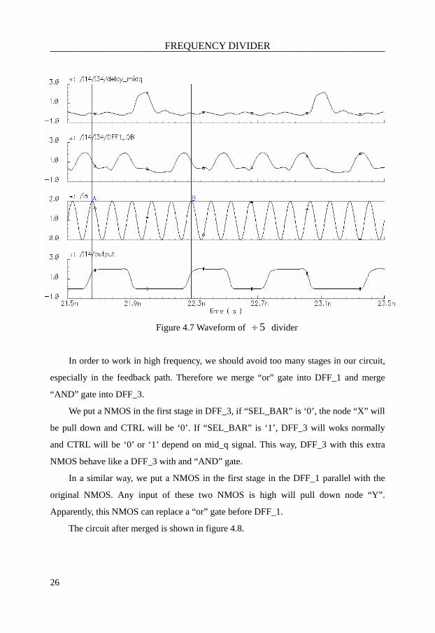
Figure 4.7 Waveform of 5÷ divider
In order to work in high frequency, we should avoid too many stages in our circuit,
especially in the feedback path. Therefore we merge “or” gate into DFF_1 and merge
“AND” gate into DFF_3.
We put a NMOS in the first stage in DFF_3, if “SEL_BAR” is ‘0’, the node “X” will
be pull down and CTRL will be ‘0’. If “SEL_BAR” is ‘1’, DFF_3 will woks normally
and CTRL will be ‘0’ or ‘1’ depend on mid_q signal. This way, DFF_3 with this extra
NMOS behave like a DFF_3 with and “AND” gate.
In a similar way, we put a NMOS in the first stage in the DFF_1 parallel with the
original NMOS. Any input of these two NMOS is high will pull down node “Y”.
Apparently, this NMOS can replace a “or” gate before DFF_1.
The circuit after merged is shown in figure 4.8.
26
FREQUENCY DIVIDER ________________________________________________________________________
Figure 4.8 Circuit of div4_5
27

FREQUENCY DIVIDER ________________________________________________________________________
Now, we have a 4/5 divider. If we put a DFF_4 after 4/5 divider, we can get an 8/10
divider. But, what we want is an 8/9 divider. This time, we try to combine “sel” signal
with output of DFF_4 (see figure 4.9).
Figure 4.9 Block diagram of div8_9
When “sel” is ‘1’, signal ‘a’ will keep ‘1’ and div4_5 will be a 4÷ divider.
Then, the whole block div8_9 will be a divider. 8÷When “sel” is ‘0’, signal ‘a’ will switch between ‘1’ and ‘0’ depends on output
signal from DFF_4. div4_5 will switch to 4÷ mode when output of DFF_4 is ‘1’
and switch to 5÷ mode when output of DFF_4 is ‘0’. Therefore, we get exact
nine input period in one cycle of DFF_4 output signal. The output signal is high for
4 input periods and low for 5 input periods. Check figure 4.10 to get more clear
idea.
28

FREQUENCY DIVIDER ________________________________________________________________________
Figure 4.10 Simulation waveforms of 9÷ divider
Again, in order to gain high speed, we merged “or” gate into DFF_3. The
circuit after merged is shown below, figure 4.11.
Figure 4.11 Circuit of div8_9
29

FREQUENCY DIVIDER ________________________________________________________________________
4.4.2 3Bcounter
Figure 4.12 Block diagram of 3Bcounter
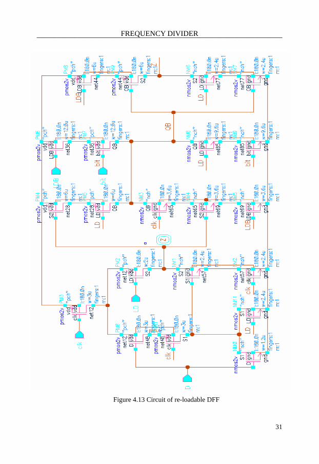
3Bcounter is made up with 3 re-loadable DFF. We take [13]’s re-loadable DFF for
reference. We found that if reload time is not long enough (about 250p s), the counter will
not work correctly after re-loading. The key issue is node “Z” (see figure 4.13) has not
discharged completely and this will make the charge kept in QB. Figure 4.14 shows how
the counter goes wrong when there is a short reload time. We want to load out2 = ‘1’,
out1 = ‘1’, out0 = ‘0’. We can see that once LD signal goes down, “out2” will be
discharged because the DFF3’s node “Z” is still high and out1 = ‘1’ and LDB = ‘1’. (Note:
out1 is clk of DFF3!!) This is incorrect and it should be modified.
30
FREQUENCY DIVIDER ________________________________________________________________________
Figure 4.13 Circuit of re-loadable DFF
31

FREQUENCY DIVIDER ________________________________________________________________________
Figure 4.14 Incorrect simulation waveforms of counter
Therefore, we add an extra NMOS to help discharge node “Z”. By adding this NMOS,
the reload time can be reduced by about 100p s. This way, the frequency divider can work
smoothly when the counter are reloaded.
Besides the counter, we put a nor_3 gate to set up control signal. The nor_3 gate is
responsible for “sel” signal. When counter counts to zero, “sel” will go high until counter
is reloaded, i.e., the count number is not zero anymore, and then “sel” goes down.
32

FREQUENCY DIVIDER ________________________________________________________________________
Figure 4.15 Circuit of modified re-loadable DFF
33
FREQUENCY DIVIDER ________________________________________________________________________
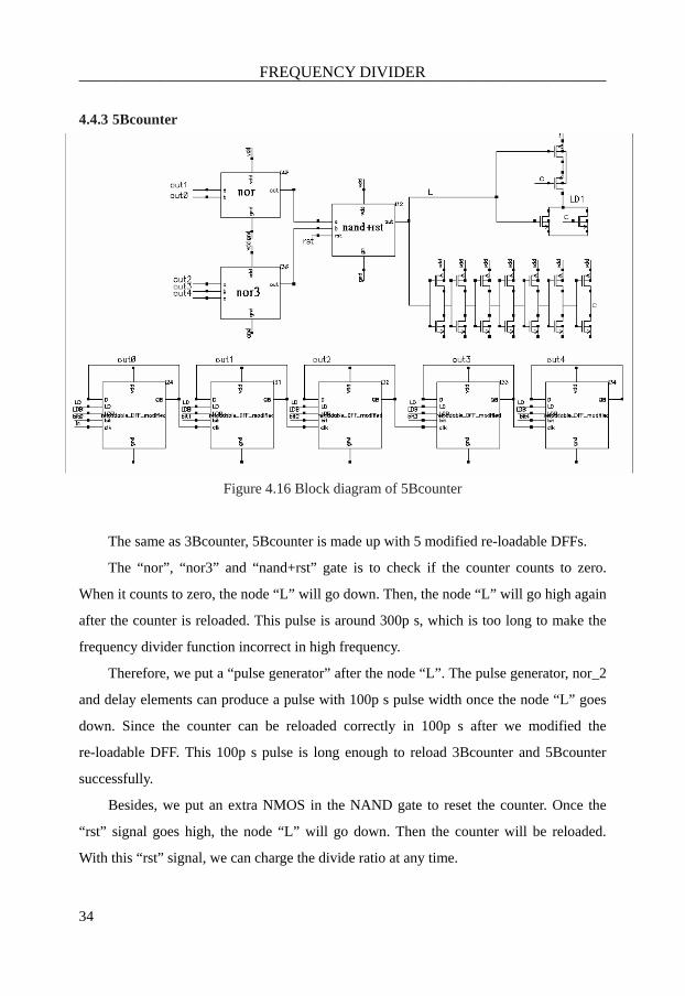
4.4.3 5Bcounter
Figure 4.16 Block diagram of 5Bcounter
The same as 3Bcounter, 5Bcounter is made up with 5 modified re-loadable DFFs.
The “nor”, “nor3” and “nand+rst” gate is to check if the counter counts to zero.
When it counts to zero, the node “L” will go down. Then, the node “L” will go high again
after the counter is reloaded. This pulse is around 300p s, which is too long to make the
frequency divider function incorrect in high frequency.
Therefore, we put a “pulse generator” after the node “L”. The pulse generator, nor_2
and delay elements can produce a pulse with 100p s pulse width once the node “L” goes
down. Since the counter can be reloaded correctly in 100p s after we modified the
re-loadable DFF. This 100p s pulse is long enough to reload 3Bcounter and 5Bcounter
successfully.
Besides, we put an extra NMOS in the NAND gate to reset the counter. Once the
“rst” signal goes high, the node “L” will go down. Then the counter will be reloaded.
With this “rst” signal, we can charge the divide ratio at any time.
34

FREQUENCY DIVIDER ________________________________________________________________________
4.5 Summary
This chapter gives information of previous work about frequency divider. We
clearly introduce our circuit and explain how we enhance the frequency divider’s
performance. In the next chapter, we will show the post layout simulation results of our
design.
35

FREQUENCY DIVIDER ________________________________________________________________________
36

SIMULATION ________________________________________________________________________
Chapter 5 Simulation 5.1 Chapter overview
In this chapter, we will show post layout simulation results of programmable
frequency divider. First, we examine that if this frequency divider can be applied to an
UWB system. Second simulation, we examine that if we can change divide ratio in a
short time. Then, we examine the robustness of the frequency divider and the working
frequency range of this prescaler. In the last section of this chapter, we put the layout of
the frequency divider.
5.2 Simulation – UWB system requirement
In this section, we want to examine if this frequency divider can work in wide
frequency range for an UWB system. We feed 13 center frequency of 13 UWB system
channel to frequency divider and divide these input signals with different divide ratio to
get the same output frequency. Because these output signals will be fed to PFD to
compare frequency with reference signal. We should make sure the frequency divider can
produce the same output signal frequency no matter what input frequency is.
37

SIMULATION ________________________________________________________________________
The following table shows divide ratio and average power of precaler for each
input frequency at typical corner case and VDD = 2V.
BAND_ID Center frequency Divide ratio Output frequency Average power
1 3432 MHz 52 66 MHz 4.048 mW
2 3960 MHz 60 66 MHz 4.254 mW
3 4488 MHz 68 66 MHz 4.542 mW
4 5016 MHz 76 66 MHz 4.893 mW
5 5544 MHz 84 66 MHz 5.009 mW
6 6072 MHz 92 66 MHz 5.384 mW
7 6600 MHz 100 66 MHz 5.632 mW
8 7128 MHz 108 66 MHz 5.532 mW
9 7656 MHz 116 66 MHz 5.820 mW
10 8184 MHz 124 66 MHz 5.927 mW
11 8712 MHz 132 66 MHz 6.512 mW
12 9240 MHz 140 66 MHz 6.441 mW
13 9768 MHz 148 66 MHz 6.679 mW
38

SIMULATION ________________________________________________________________________
The following pictures are waveforms of each input frequency and output
frequency. You can see that each output frequency with period around 15.15ns, i.e., 66
MHz.
Figure 5.1 Simulation waveform at 3432 MHz
39

SIMULATION ________________________________________________________________________
Figure 5.2 Simulation waveform at 3960 MHz
Figure 5.3 Simulation waveform at 4488 MHz
40

SIMULATION ________________________________________________________________________
Figure 5.4 Simulation waveform at 5016 MHz
Figure 5.5 Simulation waveform at 5544 MHz
41

SIMULATION ________________________________________________________________________
Figure 5.6 Simulation waveform at 6072 MHz
Figure 5.7 Simulation waveform at 6600 MHz
42

SIMULATION ________________________________________________________________________
Figure 5.8 Simulation waveform at 7128 MHz
Figure 5.9 Simulation waveform at 7656 MHz
43
SIMULATION ________________________________________________________________________
Figure 5.10 Simulation waveform at 8184 MHz
Figure 5.11 Simulation waveform at 8712 MHz
44

SIMULATION ________________________________________________________________________
Figure 5.12 Simulation waveform at 9240 MHz
Figure 5.13 Simulation waveform at 9768 MHz
45
SIMULATION ________________________________________________________________________
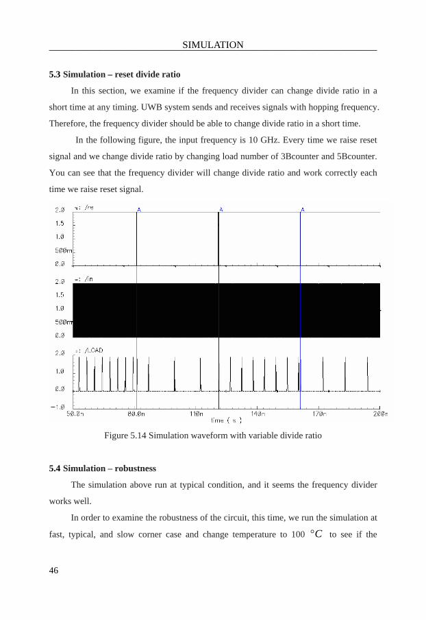
5.3 Simulation – reset divide ratio
In this section, we examine if the frequency divider can change divide ratio in a
short time at any timing. UWB system sends and receives signals with hopping frequency.
Therefore, the frequency divider should be able to change divide ratio in a short time.
In the following figure, the input frequency is 10 GHz. Every time we raise reset
signal and we change divide ratio by changing load number of 3Bcounter and 5Bcounter.
You can see that the frequency divider will change divide ratio and work correctly each
time we raise reset signal.
Figure 5.14 Simulation waveform with variable divide ratio
5.4 Simulation – robustness
The simulation above run at typical condition, and it seems the frequency divider
works well.
In order to examine the robustness of the circuit, this time, we run the simulation at
fast, typical, and slow corner case and change temperature to 100 to see if the C°
46

SIMULATION ________________________________________________________________________
circuit can still work in worse condition.
At typical and fast corner case, the frequency divider works well in room
temperature. However, there are some problems for higher temperature environment and
the slow corner case.
At room temperature and slow corner case, the frequency divider only can work
well at frequency lower than 8.2GHz. At 100 , typical corner case won’t work above
9.3 GHz and slow corner case won’t work above 8 GHz.
C°
In order to fix these problems, we decide to use higher VDD voltage. If we set
VDD = 2.5 V, the frequency divider can works well even at slow corner case at 100
environment. The trade off is the higher VDD cause much more power consumption. At
10 GHz, typical corner case, room temperature, the power consumption rise from 6.8
mW to 12.7 mW.
C°
Because the frequency divider with VDD = 2 V can work well in all cases at
frequency below 8 GHz. Our suggestion is that if the frequency divider is applied to a
transceiver which transmits signal only between channels #1, #2, #3. Then, the VDD
could be set to 2 V to save power consumption.
For the transceiver which transmits signal across #4, #5, the VDD should be set to
2.5V to make sure the functionality and performance of the frequency divider.
5.5 Simulation – working range
Last, we also examine working range of this frequency divider.
At typical corner case and VDD = 2V, the lowest frequency is 800 MHz and
highest frequency is 10.4 GHz. The minimum acceptable input peek-to-peek voltage at
10 GHz is 1.1 V (The offset voltage is 1 V).
At typical corner case and VDD = 2.5V, the lowest frequency is 2.4 GHz and
highest frequency is 11.2 GHz. The minimum acceptable input peek-to-peek voltage at
10 GHz is 1.76 V (The offset voltage is 1 V).
47

SIMULATION ________________________________________________________________________
5.6 Layout
Figure 5.15 Top view of layout
48

CONCLUSION ________________________________________________________________________
Chapter 6 Conclusion 6.1 Conclusion
In this thesis, the design of a low-cost, high speed programmable frequency divider
has been presented. It is fabricated using the tsmc CMOS 0.18um process. Simulation
results have been presented for the frequency divider. The primary use of such frequency
divider is in the area of Ultra Wide band system.
6.2 Problems encountered
Before this work, we don’t have experience using TSPC to design circuits working
at high frequency. We spent so much time on tuning sizes of each NMOS and PMOS.
Tracing signals to find which MOS should be resized and tuning the sizes without
causing another problem. It is really time-consuming but we learn a lot from it.
6.3 Future improvements
Because we use asynchronous frequency divide structure, there will be a jitter
problem in the output signal. It can be solved by adding a DFF between the output signal
and the next stage, i.e. the phase frequency detector (PFD). The input clock signal to this
extra DFF could be VCO output signal. In this way, we can cancel the jitters caused by
the asynchronous structure.
Furthermore, we use cadence DIVA to get analog-extracted layout. This tool only
extracts parasitic capacitance but no parasitic resistance. The performance of the
frequency divider after manufactured may become worse. Maybe we need another tool to
tell us information of parasitic resistance, and then we can modify the transistor size to
get better performance after manufacturing.
49

CONCLUSION ________________________________________________________________________
50

REFERENCE ________________________________________________________________________
Reference [1] Chang, B., Park, J., and Kim, W.: ‘A 1.2GHz CMOS dual-modulus frequency divider
using new dynamic D-type flip-flops’, IEEE J. Solid-State Circuits, 1996, 31, (5), pp.
749–752
[2] Craninckx, J., and Steyaert, M.: ‘A 1.75-GHz/3-V dual-modulus divide-by-128/129
frequency divider in 0.7-mm CMOS’, IEEE J. Solid-State Circuits, 1996, 31, (7), pp.
890–897
[3] Yang, C.-Y., Dehng, G.-K., Hsu, J.-M., and Liu, S.-I.: ‘New dynamic flip-flops for
high-speed dual-modulus frequency divider’, IEEE J. Solid-State Circuits, 1998, 33, (10),
pp. 1568–1571
[4] Yan, H., Biyani, M., and Kenneth, K.O.: ‘A high-speed CMOS dual phase
dynamic-pseudo NMOS ((DP)2) latch and its application in a dual-modulus frequency
divider’, IEEE J. Solid-State Circuits, 1999, 34, (10 ), pp. 1400–1404
[5] Benachour, A., Embabi, S., and Ali, A.: ‘A 1.5GHz, Sub-2mW CMOS dual-modulus
frequency divider’. Proceeding. 1999 Custom Integrated Circuits Conference, 1999, pp.
613–616
[6] Krishnapura, N., and Kinget, P.: ‘A 5.3-GHz programmable divider for HiPerLAN in
0.25-mmCMOS’, IEEE J. Solid-State Circuits, 2000, 35, (7), pp. 1019–1024
[7] Chi, B.; Shi, B.; ‘New implementation of phase-switching technique and its
applications to GHz dual-modulus frequency dividers ’, IEEE Proceeding.-Circuits
Devices System, Vol. 150, No. 5, October 2003
51
REFERENCE ________________________________________________________________________
[8] Pellerano, S.; Levantino, S.; Samori, C.; Lacaita, A.L.; A 13.5-mW 5-GHz frequency
synthesizer with dynamic-logic frequency divider , Solid-State Circuits, IEEE Journal
of , Volume: 39 , Issue: 2 , Feb. 2004 Pages:378 - 383
[9] Vaucher, C.S., Ferencic, I., Locher, M., Sedvallson, S., Voegeli, U., and Wang, Z.:
‘A family of low-power truly modular programmable dividers in standard 0.35-mm
CMOS technology’, IEEE J. Solid-State Circuits, 2000, 35, (7), pp. 1039–1045
[10] Sulaiman, M.S.; Khan, N.: ‘A novel low-power high-speed programmable dual
modulus divider for PLL-based frequency synthesizer ’, Semiconductor Electronics, 2002.
Proceedings. ICSE 2002. IEEE International Conference on , 19-21 Dec. 2002
Pages:77 – 81
[11] Wohlmuth, H.-D.; Kehrer, D.: ‘A 15 GHz 256/257 dual-modulus frequency divider
in 120 nm CMOS ’, European Solid-State Circuits, 2003. ESSCIRC '03. Conference
on , 16-18 Sept. 2003 Pages:77 - 80
[12] Dong-Jun Yang; O, K.K : ‘A 14-GHz 256/257 dual-modulus frequency divider with
secondary feedback and its application to a monolithic CMOS 10.4-GHz phase-locked
loop ’, Microwave Theory and Techniques, IEEE Transactions on , Volume: 52 , Issue:
2 , Feb. 2004 Pages:461 - 468
[13] M.A DO, X.P. Yu, J.G Ma : ‘A 2G programmable counter with new re-loadable D
flip-flop’ IEEE 2003
52

53
På svenska Detta dokument hålls tillgängligt på Internet – eller dess framtida ersättare – under en längre tid från publiceringsdatum under förutsättning att inga extra-ordinära omständigheter uppstår.
Tillgång till dokumentet innebär tillstånd för var och en att läsa, ladda ner, skriva ut enstaka kopior för enskilt bruk och att använda det oförändrat för ickekommersiell forskning och för undervisning. Överföring av upphovsrätten vid en senare tidpunkt kan inte upphäva detta tillstånd. All annan användning av dokumentet kräver upphovsmannens medgivande. För att garantera äktheten, säkerheten och tillgängligheten finns det lösningar av teknisk och administrativ art.
Upphovsmannens ideella rätt innefattar rätt att bli nämnd som upphovsman i den omfattning som god sed kräver vid användning av dokumentet på ovan beskrivna sätt samt skydd mot att dokumentet ändras eller presenteras i sådan form eller i sådant sammanhang som är kränkande för upphovsmannens litterära eller konstnärliga anseende eller egenart.
För ytterligare information om Linköping University Electronic Press se förlagets hemsida http://www.ep.liu.se/ In English The publishers will keep this document online on the Internet - or its possible replacement - for a considerable time from the date of publication barring exceptional circumstances.
The online availability of the document implies a permanent permission for anyone to read, to download, to print out single copies for your own use and to use it unchanged for any non-commercial research and educational purpose. Subsequent transfers of copyright cannot revoke this permission. All other uses of the document are conditional on the consent of the copyright owner. The publisher has taken technical and administrative measures to assure authenticity, security and accessibility.
According to intellectual property law the author has the right to be mentioned when his/her work is accessed as described above and to be protected against infringement.
For additional information about the Linköping University Electronic Press and its procedures for publication and for assurance of document integrity, please refer to its WWW home page: http://www.ep.liu.se/
© Kang, Shi-Yun Wen, Hsiang-Chih


![84335 P01EDT[01] - d7z22c0gz59ng.cloudfront.net · Tamiya EXPEC GT 2.4G B/C system Tanya EXPEC GT 2.4G system Ensemble RIC Tamiya EXPEC GT 2.4G ) *Small size ESC and receiver are](https://img.dokumen.tips/doc/110x75/5d2f377688c99331798ce3f3/84335-p01edt01-tamiya-expec-gt-24g-bc-system-tanya-expec-gt-24g-system.jpg)