Embed Size (px)
Citation preview

TECHNICAL MANUAL888-2513-001
AIR AND LIQUID COOLEDDX-400 TRANSMITTER
CONTROL UNIT992-9064-002
T.M. No. 888-2513-001
Rev. B1:11-16-11© Copyright 2003, 2004
Harris Corporation
All rights reserved

Returns And ExchangesDamaged or undamaged equipment should not be returned unless written approvaland a Return Authorization is received from HARRIS CORPORATION, BroadcastSystems Division. Special shipping instructions and coding will be provided to as-sure proper handling. Complete details regarding circumstances and reasons forreturn are to be included in the request for return. Custom equipment or specialorder equipment is not returnable. In those instances where return or exchange ofequipment is at the request of the customer, or convenience of the customer, arestocking fee will be charged. All returns will be sent freight prepaid and properlyinsured by the customer. When communicating with HARRIS CORPORATION,Broadcast Systems Division, specify the HARRIS Order Number or InvoiceNumber.
UnpackingCarefully unpack the equipment and preform a visual inspection to determine thatno apparent damage was incurred during shipment. Retain the shipping materialsuntil it has been determined that all received equipment is not damaged. Locateand retain all PACKING CHECK LISTs. Use the PACKING CHECK LIST to helplocate and identify any components or assemblies which are removed for shippingand must be reinstalled. Also remove any shipping supports, straps, and packingmaterials prior to initial turn on.
Technical AssistanceHARRIS Technical and Troubleshooting assistance is available from HARRIS FieldService during normal business hours (8:00 AM - 5:00 PM Central Time). Emer-gency service is available 24 hours a day. Telephone 217/222-8200 to contact theField Service Department or address correspondence to Field Service Department,HARRIS CORPORATION, Broadcast Systems Division, P.O. Box 4290, Quincy,Illinois 62305-4290, USA. Technical Support by e-mail: [email protected]. TheHARRIS factory may also be contacted through a FAX facility (217/221-7096).
Replaceable Parts ServiceReplacement parts are available 24 hours a day, seven days a week from theHARRIS Service Parts Department. Telephone 217/222-8200 to contact the serviceparts department or address correspondence to Service Parts Department, HAR-RIS CORPORATION, Broadcast Systems Division, P.O. Box 4290, Quincy, Illinois62305-4290, USA. The HARRIS factory may also be contacted through a FAXfacility (217/221-7096).
NOTEThe # symbol used in the parts list means used with (e.g. #C001 = used with C001).

MANUAL REVISION HISTORYDX-400 AM TRANSMITTER
888-2513-001
REV. DATE ECO PAGES AFFECTED
B 01-16-04 49913 Replaced Title Page and page C-1Added this Manual Revision History Page


Guide to Using Harris Parts List InformationThe Harris Replaceable Parts List Index portrays a tree structure with the major items being leftmost in the index.The example below shows the Transmitter as the highest item in the tree structure. If you were to look at the bill ofmaterials table for the Transmitter you would find the Control Cabinet, the PA Cabinet, and the Output Cabinet. Inthe Replaceable Parts List Index the Control Cabinet, PA Cabinet, and Output Cabinet show up one indentationlevel below the Transmitter and implies that they are used in the Transmitter. The Controller Board is indented onelevel below the Control Cabinet so it will show up in the bill of material for the Control Cabinet. The tree structure ofthis same index is shown to the right of the table and shows indentation level versus tree structure level.
Example of Replaceable Parts List Index and equivalent tree structure:
The part number of the item is shown to the right of the description as is the page in the manual where the bill forthat part number starts.
Inside the actual tables, four main headings are used:Table #-#. ITEM NAME - HARRIS PART NUMBER -this line gives the information that corre-sponds to the Replaceable Parts List Index entry;HARRIS P/N column gives the ten digit Harris part number (usually in ascending order);DESCRIPTION column gives a 25 character or less description of the part number;REF. SYMBOLS/EXPLANATIONS column 1) gives the reference designators for the item (i.e.,C001, R102, etc.) that corresponds to the number found in the schematics (C001 in a bill of materialis equivalent to C1 on the schematic) or 2) gives added information or further explanation (i.e., “Usedfor 208V operation only,” or “Used for HT 10LS only,” etc.).
Inside the individual tables some standard conventions are used:A # symbol in front of a component such as #C001 under the REF. SYMBOLS/EXPLANATIONScolumn means that this item is used on or with C001 and is not the actual part number for C001.In the ten digit part numbers, if the last three numbers are 000, the item is a part that Harris haspurchased and has not manufactured or modified. If the last three numbers are other than 000, theitem is either manufactured by Harris or is purchased from a vendor and modified for use in theHarris product.The first three digits of the ten digit part number tell which family the part number belongs to - forexample, all electrolytic (can) capacitors will be in the same family (524 xxxx 000). If an electrolytic(can) capacitor is found to have a 9xx xxxx xxx part number (a number outside of the normal familyof numbers), it has probably been modified in some manner at the Harris factory and will thereforeshow up farther down into the individual parts list (because each table is normally sorted in ascendingorder). Most Harris made or modified assemblies will have 9xx xxxx xxx numbers associated withthem.The term “SEE HIGHER LEVEL BILL” in the description column implies that the reference desig-nated part number will show up in a bill that is higher in the tree structure. This is often the case forcomponents that may be frequency determinant or voltage determinant and are called out in a higherlevel bill structure that is more customer dependent than the bill at a lower level.


WARNING
THE CURRENTS AND VOLTAGES IN THIS EQUIPMENT ARE DANGEROUS. PERSONNEL MUSTAT ALL TIMES OBSERVE SAFETY WARNINGS, INSTRUCTIONS AND REGULATIONS.
This manual is intended as a general guide for trained and qualified personnel who are aware of the dangers inherent inhandling potentially hazardous electrical/electronic circuits. It is not intended to contain a complete statement of all safetyprecautions which should be observed by personnel in using this or other electronic equipment.
The installation, operation, maintenance and service of this equipment involves risks both to personnel and equipment, andmust be performed only by qualified personnel exercising due care. HARRIS CORPORATION shall not be responsiblefor injury or damage resulting from improper procedures or from the use of improperly trained or inexperienced personnelperforming such tasks.
During installation and operation of this equipment, local building codes and fire protection standards must be observed.The following National Fire Protection Association (NFPA) standards are recommended as reference:
- Automatic Fire Detectors, No. 72E
- Installation, Maintenance, and Use of Portable Fire Extinguishers, No. 10
- Halogenated Fire Extinguishing Agent Systems, No. 12A
WARNING
ALWAYS DISCONNECT POWER BEFORE OPENING COVERS, DOORS, ENCLOSURES, GATES,PANELS OR SHIELDS. ALWAYS USE GROUNDING STICKS AND SHORT OUT HIGH VOLTAGEPOINTS BEFORE SERVICING. NEVER MAKE INTERNAL ADJUSTMENTS, PERFORM MAINTE-NANCE OR SERVICE WHEN ALONE OR WHEN FATIGUED.
Do not remove, short-circuit or tamper with interlock switches on access covers, doors, enclosures, gates, panels or shields.Keep away from live circuits, know your equipment and don’t take chances.
WARNING
IN CASE OF EMERGENCY ENSURE THAT POWER HAS BEEN DISCONNECTED.
WARNING
IF OIL FILLED OR ELECTROLYTIC CAPACITORS ARE UTILIZED IN YOUR EQUIPMENT, AND IFA LEAK OR BULGE IS APPARENT ON THE CAPACITOR CASE WHEN THE UNIT IS OPENED FORSERVICE OR MAINTENANCE, ALLOW THE UNIT TO COOL DOWN BEFORE ATTEMPTING TOREMOVE THE DEFECTIVE CAPACITOR. DO NOT ATTEMPT TO SERVICE A DEFECTIVE CA-PACITOR WHILE IT IS HOT DUE TO THE POSSIBILITY OF A CASE RUPTURE AND SUBSEQUENTINJURY.
888-2513-001 iWARNING: Disconnect primary power prior to servicing.

ii 888-2513-001WARNING: Disconnect primary power prior to servicing.

FIRST-AIDPersonnel engaged in the installation, operation, maintenance or servicing of this equipment are urged to become familiarwith first-aid theory and practices. The following information is not intended to be complete first-aid procedures, it is abrief and is only to be used as a reference. It is the duty of all personnel using the equipment to be prepared to giveadequate Emergency First Aid and thereby prevent avoidable loss of life.
Treatment of Electrical Burns
1. Extensive burned and broken skin
a. Cover area with clean sheet or cloth. (Cleanest available cloth article.)
b. Do not break blisters, remove tissue, remove adhered particles of clothing, or apply any salve or ointment.
c. Treat victim for shock as required.
d. Arrange transportation to a hospital as quickly as possible.
e. If arms or legs are affected keep them elevated.
NOTEIf medical help will not be available within an hour and the victim isconscious and not vomiting, give him a weak solution of salt andsoda: 1 level teaspoonful of salt and 1/2 level teaspoonful of bakingsoda to each quart of water (neither hot or cold). Allow victim to sipslowly about 4 ounces (a half of glass) over a period of 15 minutes.Discontinue fluid if vomiting occurs. (Do not give alcohol.)
2. Less severe burns - (1st & 2nd degree)
a. Apply cool (not ice cold) compresses using the cleanest available cloth article.
b. Do not break blisters, remove tissue, remove adhered particles of clothing, or apply salve or ointment.
c. Apply clean dry dressing if necessary.
d. Treat victim for shock as required.
e. Arrange transportation to a hospital as quickly as possible.
f. If arms or legs are affected keep them elevated.
REFERENCE:
ILLINOIS HEART ASSOCIATION
AMERICAN RED CROSS STANDARD FIRST AID AND PERSONAL SAFETY MANUAL (SEC-OND EDITION)
888-2513-001 iiiWARNING: Disconnect primary power prior to servicing.

TABLE OF CONTENTSSection I
Introduction/SpecificationsScope and Purpose . . . . . . . . . . . . . . . . . . . . . . . . . . . . . . . . 1-1System Purpose . . . . . . . . . . . . . . . . . . . . . . . . . . . . . . . . . . . 1-1General Descriptions. . . . . . . . . . . . . . . . . . . . . . . . . . . . . 1-1
Section IIInstallation/Initial Turn-On
Introduction . . . . . . . . . . . . . . . . . . . . . . . . . . . . . . . . . . . . . . 2-1Delivery and Storage . . . . . . . . . . . . . . . . . . . . . . . . . . . . . . 2-1Returns And Exchanges . . . . . . . . . . . . . . . . . . . . . . . . . . . . 2-1Unpacking . . . . . . . . . . . . . . . . . . . . . . . . . . . . . . . . . . . . . . . 2-1Installation . . . . . . . . . . . . . . . . . . . . . . . . . . . . . . . . . . . . . . . 2-1TCU Rack Installation . . . . . . . . . . . . . . . . . . . . . . . . . . . 2-1Extended/Remote I/O Connections . . . . . . . . . . . . . . . . . 2-2
Preoperational Checks . . . . . . . . . . . . . . . . . . . . . . . . . . . . . 2-7Turn-On Procedure . . . . . . . . . . . . . . . . . . . . . . . . . . . . . . . . 2-7TCU Checkout . . . . . . . . . . . . . . . . . . . . . . . . . . . . . . . . . 2-7RF Drive System Checkout . . . . . . . . . . . . . . . . . . . . . . . 2-7
Section IIIOperators Guide
Scope and Purpose . . . . . . . . . . . . . . . . . . . . . . . . . . . . . . . . 3-1Function. . . . . . . . . . . . . . . . . . . . . . . . . . . . . . . . . . . . . . . . . 3-1Transmitter ON . . . . . . . . . . . . . . . . . . . . . . . . . . . . . . . . . 3-1Transmitter OFF . . . . . . . . . . . . . . . . . . . . . . . . . . . . . . . . 3-1RAISE/LOWER Power . . . . . . . . . . . . . . . . . . . . . . . . . . 3-1
Meter Readings . . . . . . . . . . . . . . . . . . . . . . . . . . . . . . . . . . . 3-1Total Power Output Reading . . . . . . . . . . . . . . . . . . . . . . 3-1Power Block Output Reading. . . . . . . . . . . . . . . . . . . . . . 3-1
Basic Operation. . . . . . . . . . . . . . . . . . . . . . . . . . . . . . . . . . . 3-1System Turn-On 400 kW . . . . . . . . . . . . . . . . . . . . . . . . . . . 3-1400 kW Shutdown . . . . . . . . . . . . . . . . . . . . . . . . . . . . . . . . 3-2A AIR/B TEST, B AIR/A TEST . . . . . . . . . . . . . . . . . . . . . 3-2Auto Switching . . . . . . . . . . . . . . . . . . . . . . . . . . . . . . . . . . . 3-2Routine Meter Readings . . . . . . . . . . . . . . . . . . . . . . . . . . . . 3-2Advanced Operation . . . . . . . . . . . . . . . . . . . . . . . . . . . . . . . 3-2
Main Menu. . . . . . . . . . . . . . . . . . . . . . . . . . . . . . . . . . . . 3-3Power Supplies Screen . . . . . . . . . . . . . . . . . . . . . . . . . . . 3-3RF Source Screen . . . . . . . . . . . . . . . . . . . . . . . . . . . . . . . 3-3Audio Input Control Screen . . . . . . . . . . . . . . . . . . . . . . . 3-4Station Control Screen . . . . . . . . . . . . . . . . . . . . . . . . . . . 3-4Transmitter Control Screen. . . . . . . . . . . . . . . . . . . . . . . . 3-4Power Block Control Screen . . . . . . . . . . . . . . . . . . . . . . 3-5Combiner Status Screen . . . . . . . . . . . . . . . . . . . . . . . . . . 3-5Monitor Select Screen. . . . . . . . . . . . . . . . . . . . . . . . . . . . 3-6Interlock Status Screen . . . . . . . . . . . . . . . . . . . . . . . . . . . 3-6
Section IVOverall System Theory
Introduction . . . . . . . . . . . . . . . . . . . . . . . . . . . . . . . . . . . . . . 4-1Function. . . . . . . . . . . . . . . . . . . . . . . . . . . . . . . . . . . . . . . . . 4-1Transmitter Control Rack . . . . . . . . . . . . . . . . . . . . . . . . . . . 4-1Transmitter Control Unit (TCU) . . . . . . . . . . . . . . . . . . . 4-1Man/Machine Interface Panel (MMI Panel) . . . . . . . . . . 4-4Programmable Logic Controller Subrack (PLCSubrack) . . . . . . . . . . . . . . . . . . . . . . . . . . . . . . . . . . . . . . 4-4Combiner Control Unit . . . . . . . . . . . . . . . . . . . . . . . . . . . 4-4Keylock Panel . . . . . . . . . . . . . . . . . . . . . . . . . . . . . . . . . . 4-4
Block Diagram Description. . . . . . . . . . . . . . . . . . . . . . . . . 4-4Serial Control. . . . . . . . . . . . . . . . . . . . . . . . . . . . . . . . . . 4-4Parallel Control . . . . . . . . . . . . . . . . . . . . . . . . . . . . . . . . 4-4
Section VMaintenance/Alignments
Introduction . . . . . . . . . . . . . . . . . . . . . . . . . . . . . . . . . . . . . 5-1TCU Alignments . . . . . . . . . . . . . . . . . . . . . . . . . . . . . . . . . 5-1Transmitter Controller Board . . . . . . . . . . . . . . . . . . . . . 5-1RF Source Board . . . . . . . . . . . . . . . . . . . . . . . . . . . . . . . 5-1Audio Control Board . . . . . . . . . . . . . . . . . . . . . . . . . . . . 5-1Testing of the ACC Operation . . . . . . . . . . . . . . . . . . . . 5-3Customer Interface. . . . . . . . . . . . . . . . . . . . . . . . . . . . . . 5-3Digital I/O Board. . . . . . . . . . . . . . . . . . . . . . . . . . . . . . . 5-3Backplane Board . . . . . . . . . . . . . . . . . . . . . . . . . . . . . . . 5-3TCU Interface Board . . . . . . . . . . . . . . . . . . . . . . . . . . . . 5-3Transmitter Display . . . . . . . . . . . . . . . . . . . . . . . . . . . . . 5-3LV Power Supply P/N 992-9067-001: . . . . . . . . . . . . . . 5-3Extender Card . . . . . . . . . . . . . . . . . . . . . . . . . . . . . . . . . 5-4
CCU Alignments . . . . . . . . . . . . . . . . . . . . . . . . . . . . . . . . . 5-4Combiner Control Unit Interface Board . . . . . . . . . . . . . 5-4Digital I/O Board. . . . . . . . . . . . . . . . . . . . . . . . . . . . . . . 5-4Analog I/O Board . . . . . . . . . . . . . . . . . . . . . . . . . . . . . . 5-4LV Power Supply: . . . . . . . . . . . . . . . . . . . . . . . . . . . . . . 5-5
Power Monitor . . . . . . . . . . . . . . . . . . . . . . . . . . . . . . . . . . . 5-5Motor Controller . . . . . . . . . . . . . . . . . . . . . . . . . . . . . . . . . 5-5Power Block System Level Alignments . . . . . . . . . . . . . . . 5-5Serial Communication . . . . . . . . . . . . . . . . . . . . . . . . . . . 5-5Forward and Reflected Power Monitoring . . . . . . . . . . . 5-5
Cooling Control Panel (in water cooled configuration). . . 5-5
Section V-AViews - TCU
Section VITroubleshooting
Scope and Purpose. . . . . . . . . . . . . . . . . . . . . . . . . . . . . . . . 6-1
Section VIIParts List
Section ATransmitter Control Unit Sub Rack
TCU subrack . . . . . . . . . . . . . . . . . . . . . . . . . . . . . . . . . . . . A-1Introduction . . . . . . . . . . . . . . . . . . . . . . . . . . . . . . . . . . . A-1RF Source Board . . . . . . . . . . . . . . . . . . . . . . . . . . . . . . . A-1Audio Control Board . . . . . . . . . . . . . . . . . . . . . . . . . . . . A-2Customer Interface Board . . . . . . . . . . . . . . . . . . . . . . . . A-4Low Voltage Power Supply System . . . . . . . . . . . . . . . . A-5
Section BCombiner Control Unit Sub-Rack
CCU Subrack . . . . . . . . . . . . . . . . . . . . . . . . . . . . . . . . . . . . B-1Introduction . . . . . . . . . . . . . . . . . . . . . . . . . . . . . . . . . . . B-1Analog I/O Board . . . . . . . . . . . . . . . . . . . . . . . . . . . . . . B-1Digital I/O Board. . . . . . . . . . . . . . . . . . . . . . . . . . . . . . . B-2Combiner Control Unit Interface Board . . . . . . . . . . . . . B-2Combiner Control Board . . . . . . . . . . . . . . . . . . . . . . . . . B-2
Low Voltage Power Supply System. . . . . . . . . . . . . . . . . . B-3Introduction . . . . . . . . . . . . . . . . . . . . . . . . . . . . . . . . . . . B-3Function . . . . . . . . . . . . . . . . . . . . . . . . . . . . . . . . . . . . . . B-3
iv 888-2513-001WARNING: Disconnect primary power prior to servicing.

Location . . . . . . . . . . . . . . . . . . . . . . . . . . . . . . . . . . . . . . B-3Block Diagram description . . . . . . . . . . . . . . . . . . . . . . . B-3Detailed circuit description/Low voltage power sup-ply board . . . . . . . . . . . . . . . . . . . . . . . . . . . . . . . . . . . . . B-4Troubleshooting Low Voltage Supplies . . . . . . . . . . . . . B-424 Volt supply breaker (CB1) trips . . . . . . . . . . . . . . . . B-4
Section CProgrammable Logic Controller
Programmable Logic Controller (PLC) . . . . . . . . . . . . . . . C-1Scope and Purpose. . . . . . . . . . . . . . . . . . . . . . . . . . . . . . C-1Function . . . . . . . . . . . . . . . . . . . . . . . . . . . . . . . . . . . . . . C-1Location . . . . . . . . . . . . . . . . . . . . . . . . . . . . . . . . . . . . . . C-1Block Diagram Description. . . . . . . . . . . . . . . . . . . . . . . C-1Reprogramming the PLC. . . . . . . . . . . . . . . . . . . . . . . . . C-1Remote I/O Scanner Modules . . . . . . . . . . . . . . . . . . . . . C-1CPU . . . . . . . . . . . . . . . . . . . . . . . . . . . . . . . . . . . . . . . . . C-1Removal/Replacement . . . . . . . . . . . . . . . . . . . . . . . . . . . C-1
Transmitter Control Panel, Transmitter DisplayBoard and Man-Machine Interface (MMI) . . . . . . . . . . . . C-2Introduction . . . . . . . . . . . . . . . . . . . . . . . . . . . . . . . . . . . C-2Function . . . . . . . . . . . . . . . . . . . . . . . . . . . . . . . . . . . . . . C-2Location . . . . . . . . . . . . . . . . . . . . . . . . . . . . . . . . . . . . . . C-2
Section DMan Machine Interface (MMI)
Man Machine Interface . . . . . . . . . . . . . . . . . . . . . . . . . . . . D-1Introduction . . . . . . . . . . . . . . . . . . . . . . . . . . . . . . . . . . . D-1Main Menu Display. . . . . . . . . . . . . . . . . . . . . . . . . . . . . D-1Power Supply Control Screen . . . . . . . . . . . . . . . . . . . . . D-1RF Source . . . . . . . . . . . . . . . . . . . . . . . . . . . . . . . . . . . . D-1Audio Input Control . . . . . . . . . . . . . . . . . . . . . . . . . . . . D-2Transmitter Control Screen . . . . . . . . . . . . . . . . . . . . . . . D-2
Station Control Screen . . . . . . . . . . . . . . . . . . . . . . . . . . . D-2Power Block Control Screen . . . . . . . . . . . . . . . . . . . . . . D-2Combiner Status Screen . . . . . . . . . . . . . . . . . . . . . . . . . . D-3Monitor Select Screen . . . . . . . . . . . . . . . . . . . . . . . . . . . D-3Interlock Status Screen. . . . . . . . . . . . . . . . . . . . . . . . . . . D-3
Operation . . . . . . . . . . . . . . . . . . . . . . . . . . . . . . . . . . . . . . . D-4Power Supplies Screen. . . . . . . . . . . . . . . . . . . . . . . . . . . D-4RF Source Screen . . . . . . . . . . . . . . . . . . . . . . . . . . . . . . . D-4Audio Input Control Screen. . . . . . . . . . . . . . . . . . . . . . . D-5Transmitter Control Screen . . . . . . . . . . . . . . . . . . . . . . . D-5Station Control Screen . . . . . . . . . . . . . . . . . . . . . . . . . . . D-5Power Block Control Screen . . . . . . . . . . . . . . . . . . . . . . D-6Combiner Status Screen . . . . . . . . . . . . . . . . . . . . . . . . . . D-6Monitor Select Screen . . . . . . . . . . . . . . . . . . . . . . . . . . . D-7Interlock Status Screen. . . . . . . . . . . . . . . . . . . . . . . . . . . D-7
Section EKeylock Panel
Scope and Purpose . . . . . . . . . . . . . . . . . . . . . . . . . . . . . . . . E-1Function . . . . . . . . . . . . . . . . . . . . . . . . . . . . . . . . . . . . . . E-1Location . . . . . . . . . . . . . . . . . . . . . . . . . . . . . . . . . . . . . . E-1Power Block Servicing. . . . . . . . . . . . . . . . . . . . . . . . . . . E-1Power Supply Transformers and Rectifier Cabinet . . . . E-1Combiner Servicing . . . . . . . . . . . . . . . . . . . . . . . . . . . . . E-1
Appendix ALightning Protection Recommendation
Introduction . . . . . . . . . . . . . . . . . . . . . . . . . . . . . . . . . . . . . a-1Environmental Hazards . . . . . . . . . . . . . . . . . . . . . . . . . . . . a-1What Can Be Done?. . . . . . . . . . . . . . . . . . . . . . . . . . . . . . . a-1AC Service Protection . . . . . . . . . . . . . . . . . . . . . . . . . . . . . a-2Conclusion . . . . . . . . . . . . . . . . . . . . . . . . . . . . . . . . . . . . . . a-3
888-2513-001 vWARNING: Disconnect primary power prior to servicing.

vi 888-2513-001WARNING: Disconnect primary power prior to servicing.

Section IIntroduction/Specifications
1.1 Scope and PurposeThis technical manual contains the information pertaining to theDX-400 Transmitter Control Unit.The various sections of this technical manual provide the follow-ing types of information for the Overall Transmitter System.
• Section I, INTRODUCTION/SPECIFICATIONS; pro-vides general manual layout, equipment description andblock diagram.
• Section II, INSTALLATION/INITIAL TURN ON; pro-vides detailed installation procedures and initial turn oninstructions.
• Section III, OPERATORS GUIDE; provides normal turnon/off procedures, taking meter readings, and transmitteroperations.
• Section III-A, CONTROLS/INDICATORS; providesidentification and functions of Transmitter Control Unitcontrols and indicators.
• Section IV, OVERALL SYSTEM THEORY; providesblock diagrams and detailed theory of operation of theoverall Transmitter Control Unit.
• Section V, MAINTENANCE/ALIGNMENTS; providesgeneral system preventive maintenance information.
• Section V-A, VIEWS - TCU• Section VI, TROUBLESHOOTING, provides simplifiedflow style troubleshooting procedures down to sub-systemlevel (for troubleshooting of Power Block, Combiner orTCU see the appropriate manual)
• Section VII, PARTS LIST; provides a parts list for theTransmitter Control Unit.
The following sub-sections provide principles of operation forboards and modules in the DX-400 Transmitter Control Unit.
• Section A, TRANSMITTER CONTROL UNIT (TCU)SUB-RACK
• Section B, COMBINER CONTROL UNIT (CCU)Subrack
• Section C, PROGRAMMABLE LOGIC CONTROL-LER (PLC) Subrack
• Section D, MAN-MACHINE INTERFACE (MMI)• Section E, KEYLOCK PANEL
For specific information on the Power Blocks or the Combinersee the appropriate manual listed below:Power Block 888-2478-201 (Liquid Cooled)Power Block 888-2421-001 (Air Cooled)DX-400 System 888-2511-001Combiner 888-2495-001/002
1.2 System PurposeThe TCU rack consists of different units working together as asingle system. Each unit is called a “sub” unit. Some sub-unitsin the TCU Rack are vendor produced items, some are Harrismanufactured items consisting of:
• TCU Rack, (when written without the Sub rack suffix),refers to entire TCU Rack and the Control System.
• TCU Subrack, (with the Subrack reference), refers to theTransmitter Control Unit Subrack
• CCUSubrack, refers to theCombinerControlUnit Subrack• MMI, refers to the Man Machine Interface control touch-screen.
• PLC, refers to the Programmable Logic Controller units inthe TCU Rack.
When vendor items are used in the transmitter, the instructionbook will limit the discussion to the use of that vendor equip-ment.The sub-racks serve as an interface between the components andthe PLC. The Combiner Control Unit (CCU) sub-rack interfacesthe combiner to the PLC and the Transmitter Control Unitsub-rack (TCU) interfaces the remaining components of thetransmitter to the PLC.
1.2.1 General Descriptions1.2.1.1 Programmable Logic ControllerThe Allen-Bradley Programmable Logic Controller (PLC) isused in the Power Blocks as well as in the TCU/CCU sub racks.The Main function of the PLC is to provide top level control andmonitoring status with the Power Blocks and the Combiner.Serial (digital) and parallel (analog) comunications are handledby modules installed into the main PLC chassis.1.2.1.2 Electronically Programmable Logic DeviceMany boards in the TCU contain Electronically ProgrammableLogic Devices (EPLD) to perform various complex logic func-tions. These EPLDs are factory programmed and contain pro-prietary information. Their function is the equivalent of manylogic gates arranged inside the EPLD. They can be thought of asdecoders; when a specific series of input conditions is met, thena preset output will occur. Their purpose is to interface manyfunctions throughout the system into one Input/Output (I/O)module in the PLC, instead of having several I/O modules.These EPLD’s also react more quickly than going through thePLC and provide many of the “quick” functions (reacting to anARC, etc.) and will provide a parallel RF Mute when needed.This is in addition to the RF Mute that will be processed by thePLC.
888-2513-001 1-1WARNING: Disconnect primary power prior to servicing.

Figure 1-1. DX-400 Overall Block Diagram
1-2 888-2513-001WARNING: Disconnect primary power prior to servicing.

Section IIInstallation/Initial Turn-On
2.1 IntroductionThis section provides information and instructions necessary forthe installation of the DX-400 Transmitting Control Rack. Eachpiece of equipment should be inspected for shipping damage.Inventory all equipment and the contents of each box and com-pare it to the packing list.
2.2 Delivery and StorageThe major components of the system are normally delivered incrates and/or shipping skids. Smaller components are shipped incardboard cartons. Any obvious damage should be noted at thetime of receipt and claims filed with the carrier. Equipmentcapable of handling a 5,500 pounds (2,500 kg) load will beneeded to unload the equipment. Extreme care should be takenduring the unloading operation to prevent injury to personnel ordamage to the equipment. If the unit is to be temporarily stored,all parts require inside storage. Do not stack items except forsmall cardboard cartons.
2.3 Returns And ExchangesDamaged or undamaged equipment should not be returned un-less a written Return Authorization is issued. When communi-cating with Harris Corporation, Broadcast Division, specify theorder number or invoice number. Include complete details re-garding circumstances and reasons for return in the request.Custom equipment or special order equipment is not returnable.In instances where return or exchange of equipment is at therequest or convenience of the customer, a restocking fee will becharged. Special shipping instructions and coding will be pro-vided to insure proper handling. All returns will be sent freightprepaid and properly insured by the customer.
2.4 UnpackingCarefully unpack all of the units and save all packing material.Inspect thoroughly for any damage incurred in shipment. Retainall PACKING CHECK LISTS to locate and identify any compo-nents or assemblies removed for shipping. Remove any shippingsupports and straps prior to initial turn-on.
NOTEAll access/exhaust holes on the top of the units should be coveredduring installation. The top of the units should remain covereduntil the initial turn-on.
2.5 InstallationPrior to installation, all related technical manuals should becarefully studied to obtain a thorough understanding of theprinciples of operation, circuitry and nomenclature. This willfacilitate proper installation and initial checkout. The installationis accomplished in the following steps:
NOTERefer to drawing 843-5523-534 in the Drawing Package for thefollowing discussion.
2.5.1 TCU Rack InstallationThe TCU Rack is shipped with all inter-connect wiring in place.The connections to the Combiner and Combiner I/O Panel willbe rolled up into the adjacent cabinets or have to bemade on-site.Connections to the Power Blocks are made to the Combiner I/OPanel located on the top/front of Bay 1.2.5.1.1 TCU/Power Block Internal Connections
a. Connect the serial communications cable (blue cable) fromthe Combiner I/O Panel A1J5, each Power Block I/O Panel6J11 inputs and 6J9 outputs, and theCoolingControl Panel(Liquid Cooled configuration only). Since this is serialcommunications, several CPUs are daisy chained (con-nected together using a cable, all pin 1’s connected to thesame wire, all pin 2’s connected to the same wire, etc.)together. 150 Ohm terminating resistors should connect
pin 1 to pin 3 at each end of each series string. See Figure2-1 and the system drawing package 843-5523-832 page6.
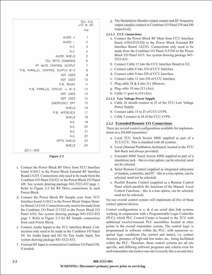
b. Connect the Power Block control and audio from TCUInterface board A10J10 and J20 to the Power Block Inter-face Board J1. Connections only need to be made from theCombiner I/O Panel J13/J18& J14/J19 to the Power BlockI/O Panel 6J12, 6J7. See system drawing package 843-5523-833. Refer to Figure 2-2 for the pin-out of the J10and J20 24 pin connection.
Figure 2-1
888-2513-001 2-1WARNING: Disconnect primary power prior to servicing.
c. Connect the Power Block RF Drive from TCU Interfaceboard A10J11 to the Power Block External RF InterfaceBoard 1A3J5. Connections only need to be made from theCombiner I/O Panel J16/J21 to the Power Block I/O Panel6J8. See system drawing package 843-5523-832 page 1.Refer to Figure 2-3 for RF Drive connections to eachPower Block.
d. Connect the Power Block RF Sample coax from TCUInterface board A10J12 to the Power Block Output Moni-tor Board 1A21J4. Connections only need to bemade fromthe Combiner I/O Panel J17/J22 to the Power Block I/OPanel 6J10. See system drawing package 843-5523-832page 1. Refer to Figure 2-3 for RF Sample connectionsfrom each Power Block.
e. Connect Audio Inputs to the TCU Interface Board. Con-nections only need to be made to the Combiner I/O PanelJ41 for Audio Input and J42 for Test Audio Input. Seesystem drawing package 843-5523-833.
f. External RF Input is connected to Combiner I/O Panel J38,if needed.
g. TheModulation Monitor output sample and RF frequencyoutput samples connect to Combiner I/O Panel J39 and J40respectively.
2.5.1.2 CCU connectionsa. Connect the Power Block RF Mute from CCU Interface
board A30A5J10/J20 to the Power Block External RFInterface Board 1A23J1. Connections only need to bemade from the Combiner I/O Panel J15/J20 to the PowerBlock I/O Panel 6J13. See system drawing package 843-5523-833.
b. Connect Cable 13 into the CCU Interface Board at J12.c. Connect cable 8 into J10 of CCU Interface.d. Connect cable 9 into J20 of CCU Interface.e. Connect cable 12 into J30 of CCU Interface.f. Plug cable 38 & 6 into J11 (Blower).g. Plug cable 10 into J13 (Arc).h. Cable 11 goes to J14 (Arc).
2.5.1.3 Low Voltage Power Supplya. Cable 16 should connect to J3 of the TCU Low Voltage
Power Supply.b. Connect cable 15 to J3 of CCU LVPS.c. Cable 5 connect to J4 of the CCU LVPS.
2.5.2 Extended/Remote I/O ConnectionsThere are several control configurations available for implemen-tation in a DX400 transmitter:
a. Local TCU Touch Screen MMI supplied as part of aTCU/CCU. This is standard with all systems.
b. Local (Manual Pushbutton facilitated, located in the TCUSub-Rack and always provided)
c. Extended MMI Touch Screen MMI supplied as part of astandalone rack – this is a true option, can be selected, neednot be selected.
d. Serial Remote Control (supplied as integrated subsystemof modem, controller, and PC - this is a true option, can beselected, need not be selected)
e. Parallel Remote Control (supplied as a Remote ControlPanel which parallels the functions of the Manual LocalControl Functions - this is a true option, can be selected,need not be selected).
No one overall control system will implement all five of thesecontrol options/choices.Control configurations a, c, & d are serial data link systemsworking in conjunction with a Programmable Logic Controller(PLC), which PLC Control Center is located in the TCU withadditional receive/transmit PLC assemblies located at otherpoints in the overall transmitter system. The control logic isprogrammed in software within the PLC, with numerous re-quired logic conditions (for control and status), i.e; contactclosures, presence of high and low states, etc., being facilitatedwithin the PLC. Therefore, these control systems are all sitespecific, and differing software programs and criteria exist foreach transmitter site (unless one site is exactly like a second site).
Figure 2-2
2-2 888-2513-001WARNING: Disconnect primary power prior to servicing.

Since the control system criteria is captured in the softwareprogram, the transmitter system must satisfy the criteria imbed-ded in the software. The system logic requirements (closed oropen contacts, high or low states, etc.), interconnect specificsexternal to the PLC, and serial data link cable segments exceptfor one or two specific requirements are found in the site specificdocumentation and are not available in this standard Tech Man-ual.General criteria for configuration “e” is available here, but sitespecific documentation must be referenced for system logicparticulars and connection specific details.2.5.2.1 Control/Monitoring Interface Data - GeneralDrawings 843-5450-039 (Station System Interconnections for aDX High Power Transmitter), 843-5523-757 (Transmitter Con-trol Unit - TCU - interface circuits), and 843-5450-655 (Sche-matic, High Power DX Extended/Remote Control), depict anextended/remote control/status system for the numerous sub-sys-tems as structured for a typical transmitter utilizing a multiple
number of Power Blocks, i.e., a DX400 Transmitter. Externalequipment cables for Transmitter control, monitor, interlock andstatus, are routed into the transmitter at the Combiner I/O Panellocated at the top of Combiner Bay 1. J6 is always supplied andconnected in a typical configuration. J7 may not be supplied butcan be used. Connections to these points should use shieldedcable and the shield connected to the chassis at the connector.The end destination of these connections is the TransmitterInterface Board located in the TCU. See interconnect schematic843-5523-833.Interlocks must be connected between pins 1 and 2 of 1AJ6Combiner I/O Panel. If interlock connections are not used, ajumper must be placed between J6, pins 1 and 2.There is a Customer Interface Board (drawing 843-5458-221) inthe TCU as well. Its input functions are primarily for considera-tions internal to the TCU andTransmitter; not for receiving directinputs from, and providing outputs to, points external to theTransmitter.
Figure 2-3 Figure 2-4
Figure 2-5
Section II, Installation/Initial Turn On
888-2513-001 2-3WARNING: Disconnect primary power prior to servicing.

2.5.2.2 Remote Control/Monitoring Interface Circuits - Gen-eral Discussion
NOTE:The application of the circuit type from those indicated below, isalready determined, the specific circuit already existing. The in-put/output interface to an external termination point being deter-mined by this already existing circuitry.
For reference, below are denoted several types of electronicinterface facilitation circuits used. Simple relay contact closuresand opens and/or electronic voltage two state sources satisfy theparticular requirements of these interfacing circuits.Figure 2-6: This is an extended control, optically isolated inputto the Transmitter. To initiate the described action, a momentary(i.e. >100mSec) ground (0V) voltage must be applied to the “x”terminal. The ground sink must sustain 24 VDC at 12mA.To prevent the described action from occuring, the cathode toanode voltage must be less than 1 VDC.Figure 2-7: Status outputs at “x” are open-collector integratedcircuit outputs to ground.When terminal “x”, externally located,receives a high state level, the transistor inside the IC turns onproviding a current sink from the status output to ground. Maxi-mum safe voltage at a status output terminal is +24VDC, and amaximum safe current into a status output is 250mA.Analog Meter Sample (J106-22): The analog meter sample out-put present here is selectable from among (1) RF Forward Power,(2) RF Reflected Power, (3) RF Amp Supply Current, (4) RFAmp Supply Voltage, and (5) Meter Mute; the selection beingmade at the TCU MMI screen. The DC voltage present corre-sponds to which one of the parameters has been selected. Theload impedance connected from the outside world, at J106-22,must be greater than or equal to 1000 Ohms.2.5.2.3 Interface Details to External Equipment
NOTE:Keep in mind that only some of the channels, with the specificidentity shown on drawings 843-5450-039-sheet 2 & 843-5450-
655-sheet 1, as well as the chart immediately following, willhave that same identity on a corresponding site specific drawing.The site specific drawing takes identity precedence. Although allof the J104 and J105 terminations are shown to be for the PAR-ALLEL remote control function, that some of these terminationsare required to satisfy Serial Data Link criteria, as well.J106 and J107 connections are less site specific intensive thanare the connections to J104 and J105.
Figure 2-6
Figure 2-7
2-4 888-2513-001WARNING: Disconnect primary power prior to servicing.

CHANNEL FUNCTION LOCATION CIRCUIT TYPE COMMENTOPTO COUPLER COMMON(TRANSMITTER CONTROL) J104-1
CH 0- TRANSMITTER OFF J104-2CH 1- HIGH POWER ON J104-3CH 2- MEDIUM POWER ON J104-4CH 3- LOW POWER ON J104-5CH 4- POWER RAISE J104-6CH 5- POWER LOWER J104-7CH 6- FAULT RESET J104-8CH 7- RF MUTE J104-9CH 8- NOT USED J104-10CH 9- METER SELECT A0 J104-11CH 10- METER SELECT A1 J104-12CH 11- METER SELECT A2 J104-13
SHIELD (GROUND) J104-14
PARALLEL REMOTE CONTROL INPUTS (TCU Transmitter Interface Bd)
FIG 2-6 LOW STATE ACTIVATES FUNCTION
Table 2-1
CHANNEL FUNCTION LOCATIONCIRCUIT
TYPE COMMENTOPTO COUPLER COMMON(TRANSMITTER CONTROL) J104-15
CH 0- PB TEST LOAD INTLK J104-16CH 1- STATION LOAD INTLK J104- 17CH 2- EXT RF SW #2 POS 1 STATUS J104-18CH 3- EXT RF SW #2 POS 2 STATUS J104-19CH 4- EXTERNAL ARC 1 J101-20CH 5- EXTERNAL ARC 2 J104-21CH 6- EXT RF SW #1 POS 1 STATUS J104-22CH 7- EXT RF SW #1 POS 2 STATUS J104-23
SHIELD (GROUND) J104-24
PARALLEL STATION STATUS INPUTS (TCU Transmitter Interface Bd)
FIG 2-6 LOW STATE ACTIVATES FUNCTION
Table 2-2
CHANNEL FUNCTION LOCATION CIRCUIT TYPE COMMENTCH 0- TRANSMITTER OFF J105-1CH 1- HIGH POWER ON J105-2CH 2- MEDIUM POWER ON J105-3CH 3- LOW POWER ON J105-4CH 4- TRANSMITTER FAULT J105-5CH 5- PB FAULT J105-6CH 6- COMBINER FAULT J105-7CH 7- PS FAULT J105-8
STATUS OUTPUT VCC J105-9STATUS COMMON J105-10SHIELD (GROUND) J105-11
PARALLEL REMOTE STATUS OUTPUTS (TCU Transmitter Interface Bd)
ACTIVE LOW OUTPUTSFIG 2-7
Table 2-3
Tables 2-1 through 2-6 provide function and connector pin details for the Parallel Control Mode.
Section II, Installation/Initial Turn On
888-2513-001 2-5WARNING: Disconnect primary power prior to servicing.

CHANNEL FUNCTION LOCATION CIRCUIT TYPE COMMENT
CH 0-STATION CONTROL - NC(No Connection) J105-12
CH 1- STATION CONTROL - NC J105-13CH 2- STATION CONTROL - NC J105-14CH 3- STATION CONTROL - NC J105-15CH 4- STATION CONTROL - NC J105-16CH 5- STATION CONTROL - NC J105-17CH 6- EXT RF SW #1 POS 1 CONTROL J105-18CH 7- EXT RF SW #1 POS 2 CONTROL J105-19
CONTROL COMMON J105-20
PARALLEL STATION CONTROL OUTPUTS (TCU Transmitter Interface Bd)
ACTIVE LOW OUTPUTSFIG 2-7
Table 2-4
FUNCTION LOCATIONEXTERNAL INTERLOCK 1 OUTPUT J107-1EXTERNAL INTERLOCK 1 INPUT J107-2SHIELD (GROUND) J107-3EXTERNAL INTERLOCK 2 OUTPUT J107-4EXTERNAL INTERLOCK 2 INPUT J107-5SHIELD (GROUND) J107-6REMOTE EMERGENCY OFF INPUT J107-7REMOTE EMERGENCY OFF COMMON J107-8SHIELD (GROUND) J107-9NC (No Connection) J107-10NC J107-11NC J107-12
INTERLOCK INTERCONNECTS(TCU Transmitter Interface Bd)
Table 2-5
FUNCTION LOCATIONPROGRAM AUDIO INPUT L (+) MONO J106-1PROGRAM AUDIO INPUT L (-) MONO J106-2PROGRAM AUDIO INPUT R (+) J106-3PROGRAM AUDIO INPUT R (-) J106-4SHIELD (GROUND) J106-5TEST AUDIO INPUT L (+) MONO J106-6TEST AUDIO INPUT L (-) MONO J106-7TEST AUDIO INPUT R (+) J106-8TEST AUDIO INPUT R (-) J106-9TEST COMMON J106-10MONITOR AUDIO INPUT L (+) MONO J106-11MONITOR AUDIO INPUT R (+) J106-12MONITOR AUDIO INPUT COMMON (-) J106-13MONITOR AUDIO OUTPUT L (+) MONO J106-14MONITOR AUDIO OUTPUT R (+) J106-15MONITOR AUDIO OUTPUT COMMON (-) J106-16SHIELD (GROUND) J106-17NC (No Connection) J106-18NC J106-19NC J106-20NC J106-21ANALOG METER SAMPLE OUTPUT J106-22COMMON J106-23SHIELD (GROUND) J106-24
ANALOG I/O INTERCONNECTS (TCU Transmitter Interface Bd)
Table 2-6NOTE: For J106-22 the external load must be 1000 Ohms or greater.
2-6 888-2513-001WARNING: Disconnect primary power prior to servicing.
2.6 Preoperational ChecksThese preoperational checks are performed under the assumptionthat the equipment has been properly installed, that there is nodamage to any components, that all interconnections have beenproperly completed, that the correct AC power supply has beenconnected, and that all cabinets have been individually connectedto the station earth ground.Refer to the DX-200 Power Block and Combiner technicalmanuals for preoperational checkout procedures to be followedfor each unit.
WARNING
ALL DOORS AND PANELS ON ALL UNITS MUST BE CLOSEDAND LATCHED PRIOR TO CHECKOUT PROCEDURES.
2.7 Turn-On ProcedureThe following procedures are intended as a guide for turning onthe system, optional procedures may be used or the order maychanged if required.
2.7.1 TCU CheckoutAfter the TCU has been connected to the Power Blocks and theCombiner it is ready to check out.
a. Make sure all power to the combiner is turned off.b. Re-seat all cards in the TCU and CCU sub-racks.c. Turn on the 220VAC single phase to the Combiner with
the wall disconnect. There should be 220VAC at the outputof A1FL3 (Combiner ACMains) and the output of A1FL1(TCU AC Mains). If not check the wall breaker or fuses.
d. Turn on the Low Voltage Supply breakers on the TCU andCCU Low Voltage Power Supplies.
NOTEAlways turn on the Low Voltage breaker first and turn them offlast to have control of the other circuits.
e. Turn on the MMI screen (Man Machine Interface).f. Adjust R34 on the LowVoltage Power Supply Board in the
TCU and CCU for ≅4.1 V at ACMains Sample TP1.g. Adjust R34 up and down until DS1, 2 or 3 is illuminated,
notice that thiswill produce anAC fault on theMMIPowerSupplies screen and notice that bit 0 on the PLC inputmodule will extinguish.
h. Return R34 to the position where TP1 reads 4.1 V.i. Press the control buttons on the Transmitter Display panel
and watch the PLC input module associated with the TCU(on the right side of the TCU rack). Press the low powerbutton-light 4 will go out momentarily. Medium-light 3will go out. High-light 2 will go out. Lower-light 6 goesout. Raise-light 5 goes out. OFF-light 1 goes out momen-tarily.
j. After assuring that the actual transmitter power is 400 kW(adjusting power output on the Analog I/O Board) check
the indication on the MMI display. Then, on the Transmit-ter Display panel, adjust R29 for a match with the MMIreading on the LCD display.
k. Remove wires at J107 on the TCU Interface Board pins 1to 2 and 4 to 5, observe an external interlock on theInterlock Status screen.
l. Remove wire from J18-16 and observe a Combiner inter-lock.
m. Short J10-17 to ground to observe a PowerBlock interlock,repeat for each Power Block.
n. On the TCUControl Board check TP3 (clk A) for approxi-mately 1 Hz and TP2 (clk B) for greater than 5 kHz andless than 10 kHz.
o. On theAudioControl Board ground theCarrier Test PointsTP11, 13 and 15, observe a fault on the Audio ControlScreen.
p. Ground the Balance test points TP10, 12 and 14, alsoobserve an Audio Fault.
q. Measure 2.38 volts at the Balance TP10, 12 and 14 withACC off.
r. Measure 1.4 volts at the Carrier TP11, 13 and 15withACCoff.
s. With ACC on measure 2.3 volts for Balance and .74 voltsfor Carrier and 1.6 volts at ACC TP6.
t. Input audio signal into Combiner I/O Panel 1AJ41 (pin1=gnd, pin ‘+’, pin 3=’-’) to show program input on theMMI screen. Connect to Combiner I/O Panel 1AJ42 (pin1 = gnd, pin 2=’+’, pin 3=’-’) to show Test Audio input.
u. On the RF Source Board, LEDs DS1 through DS9 shouldbe illuminated. Toggle S13, all LEDs except DS8 and 9should go out. Toggle S13 again, all LEDs should light.
v. On the RF Source screen, with Auto select on, manuallyshort out crystal A and observe the screen switch to Osc.B. Do the same with crystal B and observe a switch backto Osc. A.
w. Connect Program Audio to 1AJ41. Connect Test Audio to1AJ42. Check signal on R31 and R28 for the audio at theheadphone jack.
x. On the monitor screen, select audio or test signal to moni-tor. Then, apply +10 dBmor approximately 8v p-p of audio(audio or test signal - depending onwhat had been selectedin the first part of this paragraph) and set the bargraph onthe Transmitter Display to 100% for program and testinputs.
2.7.2 RF Drive System CheckoutVerification of the RF drive system will be required prior toturning on the Combiner/Power Blocks.2.7.2.1 Transmitter RF Drive Inputs
a. Measure the frequency on JP2-2 on the External RF Inter-face on each Power Block, the frequency measured shouldbe the same as the operating frequency. Verify that thegreen LED indicators on the RF Source board are lit.
Section II, Installation/Initial Turn On
888-2513-001 2-7WARNING: Disconnect primary power prior to servicing.

2-8 888-2513-001WARNING: Disconnect primary power prior to servicing.

Section IIIOperators Guide
3.1 Scope and PurposeThis section provides normal turn on/turn off and operatingprocedures, meter readings and transmitter operation from theTCU rack on the Man Machine Interface (MMI) panel and theTransmitter Display board. For fault indications see the trou-bleshooting section.
3.2 FunctionThe function of the Transmitter Display Board and theMan-Ma-chine Interface (MMI) is to provide a centralized control andmonitoring location. TheMMI is used for control andmonitoringof all functions in the combiner, upper level control of the PowerBlock and monitoring of the Rectifier Cabinets and Coolingsystem, if configured as a liquid cooled transmitter. The MMIutilizes a touch screen for very simple, straight forward operationof the transmitter. The Transmitter Control Panel provides toplevel control of the transmitter with conventional push-buttonsand monitoring with an LCD display.
3.2.1 Transmitter ONOn the MMI screen starting at the Main Menu touch the Go ToPanel “TXCONTROL”. The Screen labeled Transmitter ControlPanel will appear and allow the operator to select LOW, ME-DIUM or HIGH ON power levels for the system. All PowerBlocks will receive the same commands when these levels areselected from this screen. Transmitter readings; Forward Power,Reflected Power, PA Voltage and PA Current are displayed on abar-graph and a digital reading.
NOTE:These top level commands (LOW, MEDIUM, HIGH ON) will beapplied ONLY to the Power Blocks that are selected for outputto the antenna (combined). If a Power Block is selected to thetest load, it will NOT receive the power level commands.
3.2.2 Transmitter OFFFrom the Main Menu on the MMI screen, Go To Panel “TXCONTROL”. The Transmitter Control Panel screen will appearallowing the operator control of the entire transmitter powerincluding the OFF command. All Power Blocks will receive thesame Off command and the entire transmitter will turn off.
NOTE:The OFF command goes ONLY to the Power Blocks selected tothe combined mode (routed to the antenna). A Power Block thatis routed to the Test Load will not receive the OFF command.
Emergency OFF buttons are located at each Power Block Recti-fier cabinet and one at the Combiner Transmitter Control Unit..The large red emergency OFF buttons are pushed for OFF andmust be pulled out before the transmitter can be turned on again.Pressing any of these buttonswill turn OFF the entire transmitter.
NOTE:Emergency OFF activation will turn off all Power Blocks, in-cluding any that are in test mode.
3.2.3 RAISE/LOWER PowerFrom the “TRANSMITTER CONTROL” screen on the MMI ortheDisplayBoard, PowerRAISE andLOWER functions are sentto all Power Blocks to raise or lower each Power Blocks outputpower.
3.3 Meter ReadingsMost of theMMI screens give readings of forward power of eachPower Block and two screens give a total power output reading.
3.3.1 Total Power Output ReadingThe MAIN MENU screen shows total power output of thecombiner in addition to power output of each Power Block, theTRANSMITTER CONTROL PANEL also shows total com-bined power out and reflected power at the Combiner. TheTransmitter Display Board also shows the total power output onthe LCD read-out.
3.3.2 Power Block Output ReadingPower Output of each Power Block can be monitored from mostof the screens on the MMI.
• MAIN MENU• POWER SUPPLIES• RF SOURCE• STATION CONTROL• POWER BLOCK CONTROL• COMBINER STATUS• MONITOR SELECT
3.4 Basic OperationThis operational procedure is presented under the assumptionthat theDX-400 Transmitting System has been properly installedand checked out.
WARNING
ALL ACCESS PANELS AND DOORS MUST BE CLOSED ANDLATCHED. DO NOT BYPASS INTERLOCK SAFETY SWITCHESOR KEYLOCK SYSTEM.
3.5 System Turn-On 400 kWa. Turn ON the Primary Disconnect switch on the Trans-
former Cabinet and all secondary voltages.b. Ensure that the REMOTE/LOCAL switch in each Power
Block is in the REMOTE position.c. Ensure that Antenna position has been selected on the
COMBINER STATUS screen. (A+B AIR).
888-2513-001 3-1WARNING: Disconnect primary power prior to servicing.

d. Verify that the PB1 and PB2 indicators are illuminatedgreen at the Antenna on the MMI screen.
e. Depress the Go To MAIN MENU pushbutton on theCOMBINER STATUS screen and enter the TRANSMIT-TER CONTROL screen.
f. Depress the HIGH ON button and observe the following:1. Each Power Block goes through the power step up
sequence.2. Each Power Block is operating at 200 kWoutput as read
on the Power Block front panel meter and that no redindicators are present on the ColorStat™ front panel ofeach Power Block.
3. The total power indicated on the MMI TRANSMIT-TER CONTROL PANEL is 400 kW and no fault indi-cations.
g. Observe and record the following meter readings on theMMI(Man Machine Interface).1. Verify that the Forward Power meter reads 400 kW.2. Verify that the Reflected Power meter reads 0 kW.3. Verify that the Reject Power reads 0 kW on the RF
SOURCE screen for each Power Block.NOTE:
It is likely that there will be some small amount of reject power,however if there is a significant indication on the meter see theRF Source board description in the TCU section.
CAUTIONIF THE ABOVE OBSERVATIONS/READING PROCEDURES ARENOT CORRECT, PRESS THE OFF PUSHBUTTON AND CONTACTQUALIFIED MAINTENANCE PERSONNEL IMMEDIATELY.
3.6 400 kW ShutdownDepress the OFF pushbutton on the TRANSMITTER CON-TROL screen to turn off all Power Blocks.
3.7 A AIR/B TEST, B AIR/A TESTWith the Transmitter operating at 400kW it is possible to switchto A AIR operation with minimal delay.
a. From the MAIN MENU press the COMBINER STATUSGo To Panel.
b. At the COMBINER STATUS screen, press the A AIR/BTEST. Press MODE ENTER to carry out this command.The following will then occur.1. The Power Blocks will receive an RF Mute command.2. The RF Contactors in the Combiner will switch the
Power Block IN TEST.3. The Power Block being taken off will shut down.4. The remaining Power Block will go to 1/4 power of
previously selected power level, but muted.5. The RF Mute will be lifted.
6. The Power Block will go to 1/4 power of previouslyselected power level and then cycle to previously se-lected power level operation.
NOTE:The preceeding actions should take place within a 2 to 5 secondtime frame, depending on the transmitter frequency.
c. Observe and record the following meter readings on theCOMBINER STATUS screen:1. Verify that the Forward Power meters read 200 kW.2. Verify that the Reflected Power meter reads 0 kW.
d. With the Modulation Monitor Input Select switch to theCombiner, verify proper modulation using the modulationmeter.
CAUTIONIF THE ABOVE OBSERVATIONS/READING PROCEDURES ARENOT CORRECT, PRESS THE OFF PUSHBUTTON AND CONTACTQUALIFIED MAINTENANCE PERSONNEL IMMEDIATELY.
3.8 Auto SwitchingNOTE:
If the system automatically goes to A AIR or B AIR due to aPower Block fault, the reject load power will go up, the coolingfans will go to high speed and then the following takes place:
1. The Power Blocks will receive an RF Mute command.2. The Mode Contactors in the Combiner will switch the
Power Block Off Line.3. The Power Block being taken off will shut down.4. The remaining Power Block will go to 1/4 power of
previously selected power level, but muted.5. The RF Mute will be lifted.6. The Power Block will go to 1/4 power of previously
selected power level and then cycle to previously se-lected power level operation.
3.9 Routine Meter ReadingsLogsheets are provided for recording meter readings, copies canbe made for station records. It is suggested these readings betaken monthly at a minimum, however, more frequent logs canbe an important tool in assisting maintenance personnel.
3.10 Advanced OperationThis section discribes further operaton of the transmitter beyondthe basic level. The following sections will describe the variousscreens, their fault indications and functions.
3-2 888-2513-001WARNING: Disconnect primary power prior to servicing.

3.10.1 Main Menu3.10.1.1 Output SW (Output Earthing Switch)This block is simply a status from the micro switches on theoutput earthing switch. The display will read READY (green),EARTHED (yellow) or SW FAULT (red). The first two READYand EARTHED are self explanatory and are a reminder status.The switch cannot be moved without the use of the SCOM(Service Combiner) key in the TCU keylock panel, which meansthe transmitter cannot be turned on with the switch in the earthedposition. SW FAULT, when lit, means that the switch is not ineither of the two positions and will prevent the transmitter frombeing turned on.
NOTE:After going to the EARTHED position, the indicator will belatched in the EARTHED position (should there be a fault givingan intermittent EARTHED indication). To clear the EARTHEDposition indication, simply hit reset.
3.10.2 Power Supplies ScreenThere is one Power Supply Screen that is accessible from theMainMenu. The Power Supply button is located in the upper lefthand corner of the Main Menu. By pressing this button you willaccess the Power Supply Status screen. Any Power Supply faultwill be displayed on this screen.The color coding is basically the same as in most screens in theMMI.
• Green basically means OKAY or ON-AIR.• Red basically means FAULT or OFF-AIR.
This screen is for status of the Power Supplies only, no controlis available from this screen.3.10.2.1 1 Phase, 3 Phase indicatorIn the upper left corner of the Power Supply screen indicates theSingle phase input for the Low Voltage Power Supply and thethree phase input for the Blower Supply of the Power Blocks.3.10.2.2 AC Mains Input (this may be optional in some units)The AC mains input indicates the condition of the three phasehigh-voltage into the sub-station to be stepped down for therectifier cabinets.3.10.2.3 Three phase Voltage and Current (this may be op-
tional in some units)The three phase input voltage and current to the sub-station ismonitored for each phase A, B and C, and is digitally displayedhere. If voltage is lost for any phase the voltage readings willindicate which phase the problem is with. The current can alsobe monitored for any imbalance in the lines.3.10.2.4 Power (this may be optional in some units)The input AC power to the entire transmitter is monitored by anAllen Bradley Power Monitor and the digital display of the inputpower are displayed here including
• Kilowatts• Kilovolt-amps• Kilovolt-amps reactive• Total Power Factor
3.10.2.5 TransformerThis box represents the sub-station transformers for each rectifierand has no status indications.3.10.2.6 RectifierThe Rectifier cabinet’s output is monitored and a digital readingof the voltage and the current are displayed here. There is also afault indicator which is a summary of all faults in the RectifierCabinet. Any fault indication here would direct the technician tothe Rectifier Cabinet Display panel on the front of each rectifierto investigate the source of the fault. When no rectifier fault ispresent a green OK will be illuminated.3.10.2.7 Power BlockThe forward power of each Power Block is a good indication ofthe condition of the Power Block, and is displayed on the rightside of the screen. The condition of the Low Voltage PowerSupply AC input is indicated.3.10.2.8 TCU and CCU suppliesThe single phase input into the TCU rack is monitored. If the linevoltage is lost into the TCU rack, the AC mains indicator willchange from green to red indicating a fault. The Low VoltagePower Supply output is also indicated green when normal, red toindicate a fault. TheTCUcan have redundant LowVoltagePowerSupplies, LVPS 1 and LVPS 2 with the same monitoring. TheCCU alsomonitors the Contactor Power Supply andwill turn redif a fault occurs.
3.10.3 RF Source ScreenThe RF Source Screen is used for fault indication, RF sourceselection and RF phase adjustment.3.10.3.1 RF PresentOn the left of the RF Source screen are three indicators of RFpresent. Two Oscillators, A and B which are on the RF SourceBoard in the TCU sub rack and one indicator for an external RFsource if used. Green indicators represent the RF source ispresent and red means the RF is not present from that source.This does NOT necessarily indicate that the RF is at the rightfrequency, only that the signal LEVEL is correct.3.10.3.2 Source SelectThere are two Source select buttons. The Auto Source Selectbutton will change between AUTO and MANUAL.Manual select will enable the Source Select button under it tocontrol the input RF source. By pressing on the Source Selectbutton, the input RFwill change betweenOscillatorA,OscillatorB and the External RF input. If the source select was used on theRF Source Board, it needs to be momentarily pressed upward togive PLC control again.When Auto Select is chosen, the input RF is prioritized and willalways select the highest priority RF Source when present, andwill go to the next highest priority RF Source if that RF is lost.When the higher priority RF returns, the Auto Select will switchback to it. The RF Source priority is:
• External RF• Oscillator A• Oscillator B
Section III, Operators Guide
888-2513-001 3-3WARNING: Disconnect primary power prior to servicing.

If an external RF Source is not used, the top priority source willbe Oscillator A.3.10.3.3 Power Block RF Source PresentRF detectors on the RF source board will indicate if RF is leavingthe RF Source board to go to each Power Block. The PB RFSource OK/FAULT is the last detector of the RF in the TCU rack.3.10.3.4 Power Block StatusThe Forward and Reflected power are displayed for each PowerBlock to indicate the condition of each Power Block.3.10.3.5 Reject NullThis area is used to indicate the amount of RF Phase imbalancefrom the RF source board to each Power Block. The Reject Nullbar graph and the digital readout indicates instantaneous RejectPower dissipated in the combiner’s reject load. The AverageReject Power is a digital readout of all the reject loads. Use thephase adjustments on the RF Source board to Null out the rejectpower indicating all the RF sources are in sync.
NOTE:The null indications shown are “relative” rather than actualmeasurements of RF Power.
3.10.4 Audio Input Control ScreenThe Audio Input Control screen provides control of the audiosource into all Power Blocks or any single Power Block when inTEST and control over ACC (optional).3.10.4.1 Program/Test InputOn the left side of the screen are two indicators of the conditionof the Test Input and the Program Input. These will either be aOK/Absent. The Program and Test inputs are connected to theTCU Interface board through the Combiner I/O Panel.
NOTE:There is a delay of up to one minute before this screen updateswith a change of status.
3.10.4.2 Audio into optional ACC circuitSelection of audio into the ACC circuit for the entire transmitter(all Power Blocks) is done be pressing the Program button to theleft of the ACC button on the screen. Press it to change to TESTor back to PROGRAM for the audio feeding the ACC circuit.The selected source will be indicated on the push button andavailable at each Power Block.3.10.4.3 ACCAdaptive Carrier Control is turned ON or OFF by pressing theACCbutton on the screen.AudiowithACC is fed to all thePowerBlocks through the Program input when selected.3.10.4.4 Program Audio Configuration ErrorThis error message will flash when the Power Blocks “on-air”do not have the same source audio. When all are configured thesame, this message will not appear.3.10.4.5 Audio SelectSelection of audio to each Power Block is done be pressing eachPower Block button on the screen. Press it to change to TEST orback to PROGRAM. The selected source for that Power Blockwill be indicated on the push button.
3.10.4.6 Power Block Audio Driver Fault DetectorOn the Audio Input Control Board, there is an audio detector oneach line as the signal leaves the board. This is the last indicationof the audio on this board. The Power Block Audio Driverindicator will be red/FAULT if the audio driver output is notpresent for any Power Block, green/Audio Present when audiodriver output is at the output of this board. (A problem with thecarrier DC level would also cause a fault indication.)
3.10.5 Station Control ScreenThis screen selects the source of the control and also controls theCooling System pumps and gives summary faults for the coolingsystem.3.10.5.1 Station ControlAt the top of the screen is the selector button for the controlsource. Pressing the button control will change from Local,Extended, and Remote. When Local control is desired, simplypress the selector button until Local Control Active is indicated.Repeat for Remote and Extneded controls.3.10.5.2 Power Block StatusIn the center of the screen status indicates where each PowerBlock is routed through the Combiner. The Power Blocks thatare selected through the RF contactors to go to the Antenna willshowup in theCOMBINER status box. ThePowerBlocks routedto the test load appear in the TEST status box. The PB Test Loadinterlock will be indicated to the right of the screen. If an externalRF switch is used for a station load, that switch and associatedarc sensors are shown.3.10.5.3 Building Cooling Control (Optional)The control of the building fans is either automatic or manualselectable at this box.When in automaticmode, the building fanswill be enabled when required by the temperature switch. If thetemperature switch closes the fans will be turned on.When the control is manual, the building fans can be turned onand off by pressing the bldg fans button. This box will alsoindicate high building temperature, for warning only.
3.10.6 Transmitter Control ScreenThis screen will control and give status of all Power Blocks.Across the top of the screen are the power level push buttons andOFF, on the left are RAISE and LOWER. These commands aresent to all Power Blocks through the PLC.3.10.6.1 MeteringThe Transmitter Metering has bar graph and digital read outs ofForward Power, Reflected Power, PAVoltage and PACurrent forthe entire transmitter.3.10.6.2 Power Block StatusEach Power Block has a status block to indicate it’s power level,High, Medium, Low or Off. The color of the block will indicateif that Power Block is in Test by changing to YELLOW, or if ithas Faulted by changing to RED. Off Line indicates the serialcommunication has been interrupted.3.10.6.3 Control StatusIndicators directly under the Power Block Status will indicatewhere the control is sourced, Local, Extended or Remote.
3-4 888-2513-001WARNING: Disconnect primary power prior to servicing.

3.10.6.4 System StatusAt the right of the screen are overall System Status indicators thatwill be OK or Fault for each:
• Transmitter, overall condition• Combiner• Power Supply-Rectifier Cabinet• Cooling System• Subrack Communications-looks for all TCU and CCUboards in the Subracks. Under this status block are indica-tions of each of the boards the sub rack is communicating:
TCU Communications
• Digital I/O Board• Audio Control Board• RF Source Board• Customer Interface Board
CCU Communications
• Digital I/O Board• Analog Input Board
3.10.7 Power Block Control ScreenThis screen provides independent control of each Power Blockwhen they are not combined. When they are combined, controlcomes from the Transmitter Control Screen. When any PowerBlock is IN TEST, it can be individually controlled from thisscreen. Status of each Power Block is also given. Power controlfor individual Power Blocks is always active for minor powerlevel adjustment.3.10.7.1 Power OutputThe forward and reflected power for each Power Block indicatesthe condition of each Power Block.3.10.7.2 Power LevelIn the center of the screen are the power level selectors for eachPower Block. These are only active when that Power Block is inthe test mode. When a Power Block has been switched to TestMode on the Combiner Status screen, the power level buttons forthe Power Block in-test will be active.3.10.7.3 Raise/LowerThe Raise and Lower buttons are always active and can be usedto make power output adjustments to each Power Block at anytime.3.10.7.4 Power Block OFFThis button is only active when the Power Block is in the TestMode to prevent the Power Block being turned off when in thecombined mode.
3.10.8 Combiner Status ScreenThe RESET button is an indicator reset, which will reset alllatched faults in the transmitter provided the fault is no longerpresent.The Combiner panel gives status on each of the following:
a. PB Contactor positions and Arcs in the contactor compart-ments.
b. Arcs in the Main Combiner compartments.c. Arcs in the reject load area.
d. Reject loads, Active or OK (actually a status of reject loadcurrent).
e. Reject Load Temperaturef. Output Network
1. Arc2. VSWR
3.10.8.1 SW STATUS/SW FLTThis indicator is for switch position error status. Under normaloperating conditions, the indicator will be green and say SWOK.When one of the contactors is not in the proper position, accord-ing to the commanded mode, or is stuck in between positions,the indicator will be flashing red and say SW FLT. A switch faultwill mute the transmitter.3.10.8.2 ARCThe Arc fault will light if there is an arc in one of the Contactorcompartments. Each Contactor has its own arc fault. There aretwo arc detectors in Bay 2 upper front and rear. If an arc isdetected in the upper Bay 2 rear compartment, ARC indicatorswill flash red. It will tell the operator in which compartment thefault occurred.3.10.8.3 REJECTThe reject loads have three status indicators:
a. ARC - in which all four arc detectors in the center of thecombiner are summed together so that any arc detectorwhich is triggered will cause the thin vertical REJECTARC indicator to flash red.
b. OK/ACTIVE - During normal operation the reject loadsare dissipating little or no power and the status will begreen and say OK. If a reject load were to dissipate exces-sive current (about 10kW or more), perhaps due to thefailure of a Power Block, the indicator will be flashing redand say ACTIVE. If this condition persists the PowerBlockwill be automatically taken off line and the combinermode switched.
c. TEMP OK/TEMP FAULT - During normal operation theindicator will be green and say TEMP OK. If the tempera-ture of a reject load exceeds 270 degrees F (132 degreesC), the indicator will be flashing red and say TEMPFAULT, the combiner blowers will go to maximum speedand the transmitter will be muted. After the temperaturehas been reduced to normal range, the RF mute would belifted and the transmitter should resume normal operation.
3.10.8.4 COOLINGThis block is for the combiner air cooling system, and is notrelated to the Power Block cooling system. There are three statusblocks for the cooling system:
a. AIR OK/AIRFLOW - This indicator is from the air flowmonitors and will say AIR OK and be green if the airflowfrom the blowers is sufficient. If the airflow is restricted orreduced, the indicator will be flashing red and say AIR-FLOW. The fault has a two step threshold, the first step isa small reduction in airflow at which point the transmitterpower will foldback and the second step is the fault thresh-old at which point the transmitter is shut off.
Section III, Operators Guide
888-2513-001 3-5WARNING: Disconnect primary power prior to servicing.

b. Blower Motor Controller Status - The center block is theBALDOR blower motor controller status block. There aretwo possible status/faults listed below, all of which comeup in this one window:1. BLOWER OK (green)2. BLWR FLT (red)
c. ACCESS INTERLOCK - ACCESS INTERLOCK is fromthe interlock switch on the inner panel, at the rear of thiscompartment, which covers the blowers. This panel isinstalled with screws and must be in place to operate thetransmitter. If the panel is in place, the indicator will begreen. If the panel is removed, the indicator will flash redand the transmitter will shut off.
The Combiner Mode portion of the screen (bottom section) isused to select the mode of each Power Block: A+B AIR, A+BTEST, A AIR/B TEST, B AIR/A TEST. This screen will alsodisplay positioning faults for each of the contactors. Furtherexplanation on the combiner screens is available in theCombinerManual.3.10.8.5 Power BlockOn the left side of the Combiner Status screen is the powerreading for each of the twoPowerBlocks. This is a good indicatoras to the operating condition of the Power Blocks. These displaysshould normally read 200 (for 200kW) when the transmitter isoperating at full power. These display blocks are for status andhave no function if pressed.3.10.8.6 ModeIn the block labeled Mode Control there are four selections inone box. Cycle through until the desired mode is highlighted:
a. A+BAIRb. A+B TESTc. A AIR/B TESTd. B AIR/A TEST
3.10.8.6.1 Changing Combiner Mode
To change the Combiner.
• Select the mode using the Control Buttons.• Press ‘MODE ENTER.’
Once the mode is selected, press MODE ENTER (it should beflashing) to actually make the Combiner change modes.3.10.8.6.2 Automatic Mode Switching
The combiner system is designed to automatically switch out aPower Blocks if a fault is detected. If the combiner automaticallyswitches modes due to a Power Block fault, then that PowerBlock will show up in the TEST block. There would also be ared fault block, directly above MODE ENTER, which saysAUTO SWITCHING ACTIVATED. This lets the operator knowthat themode switchwas initiated automatically. Once the Power
Block problem is corrected, pressing MODE ENTER will bringthe transmitter back to the previously selected mode.
3.10.9 Monitor Select ScreenThis screen is used to select the source of RF to be monitoredthrough a Demodulator or to monitor the Program or Test inputs.3.10.9.1 Forward PowerAt the left of the screen are indicators for each Power Blocks’forward power to indicate the condition of each Power Block.3.10.9.2 RF Sample SelectorsPressing the RF sample button for each Power Block, or the RFsample Combined button, selects the input to the Demodulatorin the TCU rack. To the right of the screen illustrates whichsource has been selected.3.10.9.3 Monitor SelectThe monitor select button will select between the Demodulator,Program input, Test input, or anExternalAMDemodulator input.By pressing on this button the audio output to an external speakeror headphones changes to the desired source.3.10.9.4 BargraphThe Transmitter Display board on the TCU rack has a bar graphto show the selected source. Like the Monitor selector, theBargraph selector will show the selected Demodulated audio,Program input, or Test input.
3.10.10 Interlock Status ScreenThe Interlock Status screen graphically illustrates the interlockchain and gives status of each stage in the chain. The switchesare drawn in the OPEN position to show it is a series circuit,however when all interlocks are satisfied the actual switch isreally CLOSED to complete the chain.The System Interlocks are two external interlocks connected tothe TCU Interface board through the Combiner I/O Panel 1AJ6,and should be jumpered closed if not used. The TCU Interlockis the Emergency OFF button on the TCU rack. It is a push toopen and pull to close switch with a large red button.The Combiner Interlock will break the chain whenever theEarthing Switch is in the “Earthed” position, blower access coveropened, the Main Key or Aux Key has been removed or theEmergency Off button is pushed.The Power Block Emergency Off button on each Rectifier Cabi-net will break the Interlock chain if pushed. The Power BlockKeylock is located in the TCU rack, if any key is removed toservice that Power Block the Interlock string will be broken forthat Power Block and that Power Block will be turned off. Formore information on the keylock system see the chapter on theKey Lock Panel.See the Combiner manual for a complete description of theCombiner Status screen.
3-6 888-2513-001WARNING: Disconnect primary power prior to servicing.
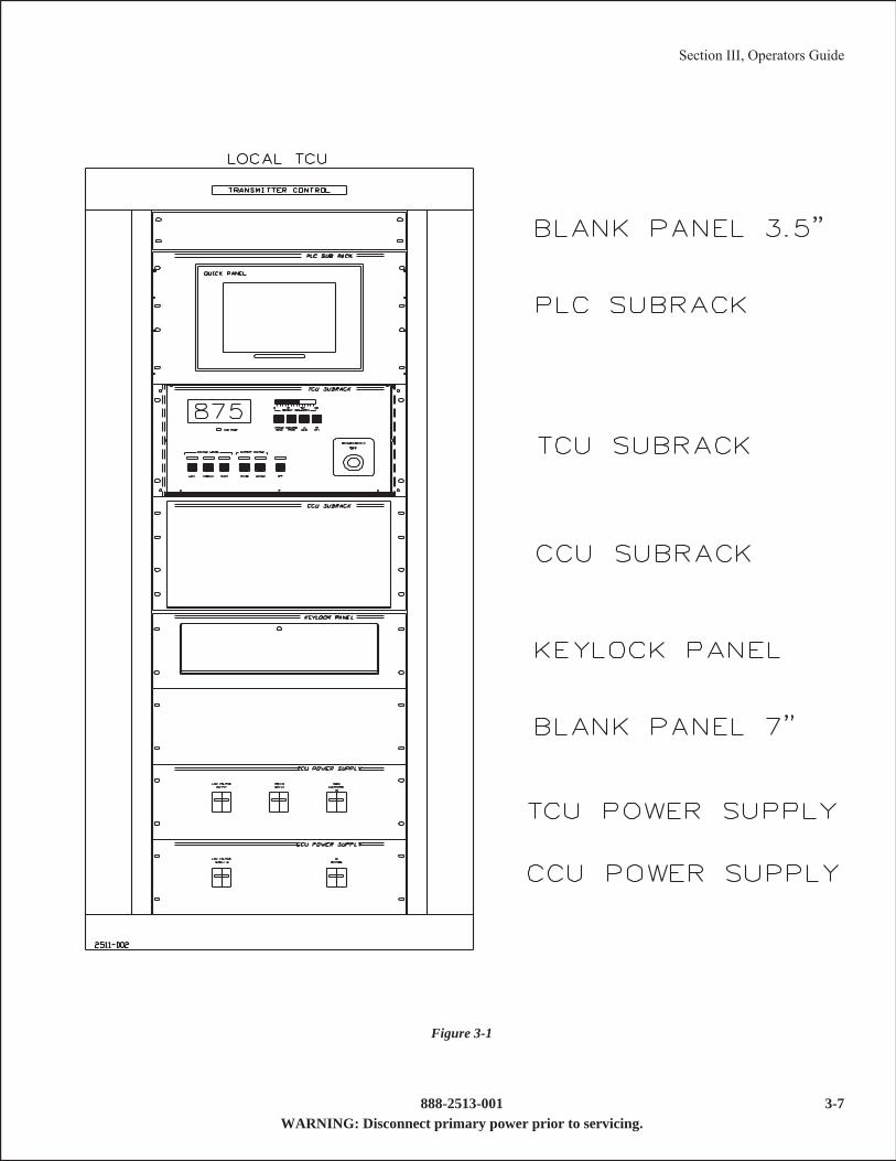
Figure 3-1
Section III, Operators Guide
888-2513-001 3-7WARNING: Disconnect primary power prior to servicing.

3-8 888-2513-001WARNING: Disconnect primary power prior to servicing.

Section IVOverall System Theory
4.1 IntroductionThis section contains the theory of operation of the Control Rackwith simple touch-screen control with extensive diagnostics.Contained in the Control Rack are sub-racks that perform differ-ent functions.
4.2 FunctionEach DX-400 transmitter has its own control system called theTransmitter Control Unit (TCU) which is located in the 2-way400kW combiner. The TCU functions include audio/RF distri-bution to the Power Blocks, control of the combiner and highlevel control of the Power Blocks. Each Power Block has its owncontrol system and can operate independently of the TCU. ThePower Block control system only takes high level commandsfrom the TCU to turn it on and off at the proper power level.
4.3 Transmitter Control RackThe transmitter Control Rack is the main control point for thetransmitter. It consists of a Transmitter Control Panel that is themain operating interface to turn the transmitter on and off at the
proper power level. It also includes a large LCD multimeter forthe top level transmitter functions. The Man/Machine Interface(MMI) Panel consists of a color touchscreen control panel thatwill allow control, status and metering of the entire transmitterincluding the combiner. Installations with an extendedMMIwillhave similar control and status reporting using an additionalMMI screen apart from the MMI screen in the combiner TCU.
4.3.1 Transmitter Control Unit (TCU)The TCU subrack contains the specialized PC boards requiredfor transmitter control which are not accommodated by the PLCsuch as RF carrier control and audio control.4.3.1.1 Subrack ComponentsThe subrack contains slide in PC boards connecting to a back-plane. This backplane is connected to a TCU Interface Panelwhich provides the connection points to all units in the transmit-ter. The slide in PC boards in the subrack are as follows:
• RF SOURCE BOARDThis board contains the two oscillators, External RF input cir-cuitry and the RF phasing circuits to ensure all Power Blocks arecombined properly.
• AUDIO CONTROL BOARDRefer to Figure 4-2 and drawing #843-5400-621 for the follow-ing discussion.
Figure 4-1 - DX-400 Overall Block Diagram
888-2513-001 4-1WARNING: Disconnect primary power prior to servicing.
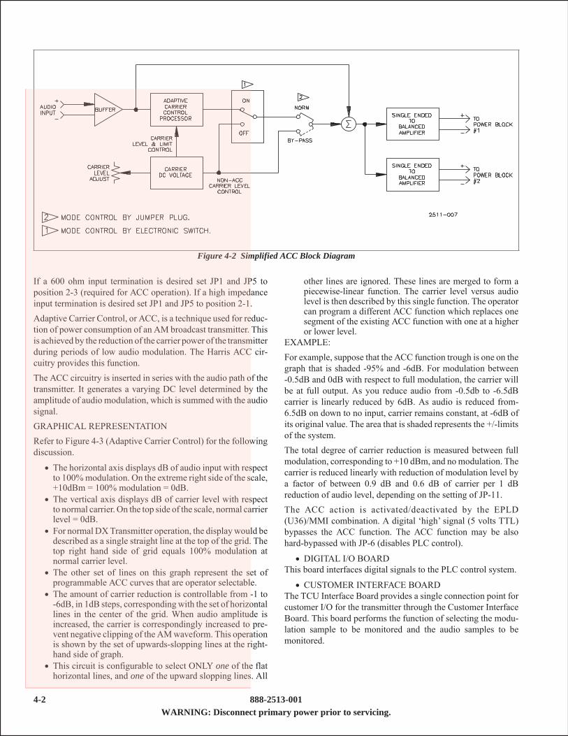
If a 600 ohm input termination is desired set JP1 and JP5 toposition 2-3 (required for ACC operation). If a high impedanceinput termination is desired set JP1 and JP5 to position 2-1.Adaptive Carrier Control, or ACC, is a technique used for reduc-tion of power consumption of an AM broadcast transmitter. Thisis achieved by the reduction of the carrier power of the transmitterduring periods of low audio modulation. The Harris ACC cir-cuitry provides this function.The ACC circuitry is inserted in series with the audio path of thetransmitter. It generates a varying DC level determined by theamplitude of audio modulation, which is summed with the audiosignal.GRAPHICAL REPRESENTATIONRefer to Figure 4-3 (Adaptive Carrier Control) for the followingdiscussion.
• The horizontal axis displays dB of audio input with respectto 100%modulation. On the extreme right side of the scale,+10dBm = 100% modulation = 0dB.
• The vertical axis displays dB of carrier level with respectto normal carrier. On the top side of the scale, normal carrierlevel = 0dB.
• For normal DXTransmitter operation, the displaywould bedescribed as a single straight line at the top of the grid. Thetop right hand side of grid equals 100% modulation atnormal carrier level.
• The other set of lines on this graph represent the set ofprogrammable ACC curves that are operator selectable.
• The amount of carrier reduction is controllable from -1 to-6dB, in 1dB steps, correspondingwith the set of horizontallines in the center of the grid. When audio amplitude isincreased, the carrier is correspondingly increased to pre-vent negative clipping of the AMwaveform. This operationis shown by the set of upwards-slopping lines at the right-hand side of graph.
• This circuit is configurable to select ONLY one of the flathorizontal lines, and one of the upward slopping lines. All
other lines are ignored. These lines are merged to form apiecewise-linear function. The carrier level versus audiolevel is then described by this single function. The operatorcan program a different ACC function which replaces onesegment of the existing ACC function with one at a higheror lower level.
EXAMPLE:For example, suppose that the ACC function trough is one on thegraph that is shaded -95% and -6dB. For modulation between-0.5dB and 0dB with respect to full modulation, the carrier willbe at full output. As you reduce audio from -0.5db to -6.5dBcarrier is linearly reduced by 6dB. As audio is reduced from-6.5dB on down to no input, carrier remains constant, at -6dB ofits original value. The area that is shaded represents the +/-limitsof the system.The total degree of carrier reduction is measured between fullmodulation, corresponding to +10 dBm, and nomodulation. Thecarrier is reduced linearly with reduction of modulation level bya factor of between 0.9 dB and 0.6 dB of carrier per 1 dBreduction of audio level, depending on the setting of JP-11.The ACC action is activated/deactivated by the EPLD(U36)/MMI combination. A digital ‘high’ signal (5 volts TTL)bypasses the ACC function. The ACC function may be alsohard-bypassed with JP-6 (disables PLC control).
• DIGITAL I/O BOARDThis board interfaces digital signals to the PLC control system.
• CUSTOMER INTERFACE BOARDThe TCU Interface Board provides a single connection point forcustomer I/O for the transmitter through the Customer InterfaceBoard. This board performs the function of selecting the modu-lation sample to be monitored and the audio samples to bemonitored.
Figure 4-2 Simplified ACC Block Diagram
4-2 888-2513-001WARNING: Disconnect primary power prior to servicing.

Figure 4-3 Adaptive Carrier Control Characteristics
Section IV, Overall System Theory
888-2513-001 4-3WARNING: Disconnect primary power prior to servicing.

4.3.2 Man/Machine Interface Panel (MMI Panel)This panel consists of a touchscreen based operator interface thatallows control, status, and metering of the overall system. Thisoperator interface is referred to as the “Man/Machine Interface”(MMI) and has various menu driven screens that include thefollowing:
• TRANSMITTER CONTROLThis control screen has the sameHigh level control and meteringavailable as pushbuttons on the control panel. In addition overalltransmitter status and simultaneous metering of the high levelreadings are displayed.
• POWER BLOCK CONTROLThere is one screen for all Power Blocks that provides individualcontrol, overall fault status monitoring and metering.
• COMBINER CONTROLThere are screens available for setting the mode of the combinerto control which Power Blocks are on the air and whether thetransmitter is operating on the air or into the test load. Otherscreens provide comprehensive status and metering of combinerfunctions.The TCU sub-rack also includes the Emergency Off Button thatwill immediately shut off the entire transmitter if needed.
4.3.3 Programmable Logic Controller Subrack(PLC Subrack)
The PLC is the central controller for the transmitter. The PLC isa modular unit consisting of a CPU, power supply, Digital inputmodules, Digital output modules, analog I/O modules and scan-ner modules. These are all serial interfaces.
4.3.4 Combiner Control UnitThe Combiner Control Unit subrack(CCU) is the heart of thecontrol system for the combiner. All control status and meteringfunctions for the combiner are physically brought together oninterface boards in the combiner subrack. The Interface boardsgroup all signals associated with Power Blockmode control. The2-Way Combiner Interface Board brings together all signalsassociated with the combiner. The signals (control, status, andmetering) are sent to the TCU which is located in a fully acces-sible compartment of the combiner. The CCU interface boardprovides an interface point between the combiner signals and theTCU. The main destinations for the combiner control signals arethe PLC (Programmable Logic Controller) and TCU subrack.Control of the Contactors in the Combiner comes from the CCUInterface board.
• ANALOG I/O BOARDThis board interfaces all analog input signals to the controlsystem to provide trigger thresholds and/or metering.
4.3.5 Keylock PanelThis section provides main interlock control keys for the trans-mitter. This includes the appropriate master keylocks to shutdown all or parts of the transmitter system for servicing.
4.4 Block Diagram DescriptionRefer to drawing #843-5450-983 page 4 for the following dis-cussion.For specific detailed circuit description, see the appropriatesection in the manual.The heart of the TCU rack is the PLC subrack which consists oftheManMachine Interface that allows the operator to control thetransmitter and provides status of various areas in the facility.The MMI works directly with the PLC Central Processing Unit(CPU). The CPU receives both digital and analog status inputsand sends digital outputs through digital and analog, input andoutput modules that are plugged into the PLC frame.Almost everything is accomplished using the Serial Controlfunction, (Control, Status andMonitoring)with the exception of:
a. RF Inputb. Audio Inputc. Mod Monitor Samplesd. Interlock Chaine. RF Mute (There are both Serial and Parallel RF Mute
functions, however the Parallel RF Mute is much faster.)
4.4.1 Serial ControlThe PLC in the TCU rack is connected to PLC units in eachPower Block and the cooling panel PLC, so each unit with a PLCcan be controlled by the TCU rack PLC. The CPU in each PLCuses input and output modules to interface with the equipment.With each CPU cycle, the PLC will check with the Power BlockPLC units for status and give any serial control that is present.Serial control is for normal control situations.
4.4.2 Parallel ControlThe TCU subrack provides parallel control to the Power Blocks.It also sends RF drive and audio to all the Power Blocks inparallel. The TCU subrack receives the control signals from thedigital output module in the PLC. These control signals arerouted through the appropriate circuit board in the subrack beforegoing to the Power Block. The TCU sends metering and statusback to the PLC digital and analog inputmodules that come fromthe Power Block.Only the RF Mute and Interlock Chain are currently used forcontrol.
4-4 888-2513-001WARNING: Disconnect primary power prior to servicing.

FUNCTION SPECIFICATIONCONTROL SYSTEM PLC basedINTERCONNECTION SYSTEM Predominately serial based interconnection with selected parallel
interconnectionsGRAPHIC MAN/MACHINE INTERFACE 10" STN Color flat panel touchscreen display for transmitter control rack.MAIN TRANSMITTER CONTROL INTERFACE Top level controls are by buttons/ lower level controls via touchscreenMAIN TRANSMITTER STATUS INDICATIONS Top level status via LEDs/all other status via touchscreenTRANSMITTER CONTROLS (top level) HIGH,MED,LOW, RAISE, LOWER, OFFTRANSMITTER STATUS (top level) HIGH,MED,LOW, RAISE, LOWER, FAULTMODE CONTROLS ON AIR/OFF AIR/TEST for each Power Block (available on touchscreen
MMI)MODE STATUS ON AIR/OFF AIR/TEST for each Power Block (available on touchscreen
MMI)MAIN TRANSMITTER METER INDICATIONS 1.5"/3.8 Ccm LCD meter for top level metering. All metering available on
touchscreenOVERALL TRANSMITTER-FWD POWER, REFLD POWER, PAV, PAI,VSWR NULL, REJECT NULL
ADDITIONAL CONTROLS Via main control touchscreen all main level controls are available inaddition to all main power block controls
ADDITIONAL STATUS All standard status indications and purchased options will be displayed aspart of the MMI system.
ADDITIONAL METERING All standard analog indications and purchased options will be displayed aspart of the MMI system.
RF CONTROL SYSTEMFUNCTION SPECIFICATION
RF PHASING Centrally located at the Transmitter control unit (TCU) on the TCU subrackRF SOURCE STATUS LEDs on RF source board and available on touchscreenCIRCUITRY LOCATION Centrally located on the RF source board at the TCU
AUDIO CONTROL SYSTEMFUNCTION SPECIFICATION
DISTRIBUTION SYSTEM ACTIVE DISTRIBUTIONSEPARATE AUDIO TEST INPUT ALLOWS POWER BLOCK IN TEST TO HAVE SEPARATE AUDIO
FEEDAUDIO SOURCE STATUS LED display on Audio control board, and available on touchscreen.
TRANSMITTER CONTROL UNIT POWER SUPPLYFUNCTION SPECIFICATION
POWER SUPPLY MODULAR SWITCHING SUPPLYINPUTAC 195 - 240VAC
INTERLOCK AND SERVICING SYSTEMFUNCTION SPECIFICATION
INTERLOCK SYSTEM KEYLOCKINTERLOCK STATUS GRAPHICAL DISPLAY OF INTERLOCK SYSTEM STATUSCOMBINER SERVICE FEATURE STANDARDEMERGENCY OFF STANDARDPOWER BLOCK ON AIR SERVICING VIA KEYLOCK SYSTEM
Section IV, Overall System Theory
888-2513-001 4-5WARNING: Disconnect primary power prior to servicing.

OTHER STANDARD FEATURESFUNCTION SPECIFICATION
AC INPUT MONITORING (input AC Volts and current atswitchgear)
Standard power monitor panel mounted in switchgear withserial interface
ON LINE TROUBLESHOOTING Specific touchscreens with troubleshooting informationON LINE MAINTENANCE Specific screens with maintenance informationSELF DIAGNOSTICS PLC system performs self diagnostics and will display fault
conditions via MMI. Transmitter system performs various selftests during turn-on.
REMOTE AND EXTENDED CONTROLFUNCTION SPECIFICATION
EXTENDED CONTROL (SERIAL) All control, status and metering functions that are available onthe local transmitter control touchscreens will be available byserial extended control
EXTENDED CONTROL PANEL Extended control via an IBM compatible PC with rackmounted monitor and printer. Extended control entry would bevia keyboard or mouse.
REMOTE CONTROL (SERIAL) All control, status and metering functions that are available onthe local transmitter control touchscreens will be available byserial remote control
REMOTE CONTROL OPERATOR INTERFACE Touchscreen panel or PC based operator interface hardware andsoftware are available as an option
REMOTE CONTROL INTERFACE Serial control interface module will be supplied as standard.Remote control operator interface hardware and software is anoption.
LOGGING/ TRENDING With pc based extended or remote unitPARALLEL INTERFACE Each transmitter has a parallel control interface available for
remote or extended control.
FLEXIBILITY/CONFIGURABILITYFUNCTION SPECIFICATION
SPARE CUSTOMER SPECIFIED DIGITAL INPUTS 16 spare customer inputs on Station Control unitSPARE CUSTOMER SPECIFIED DIGITAL OUTPUTS 16 spare customer Digital Outputs on Station Control unitSPARE CUSTOMER SPECIFIED ANALOG INPUTS 4 spare customer Analog inputs on Station Control unitCUSTOMER PROGRAMMABLE I/O 4 Customer programmable I/O available via touchscreenFIELD UPDATES OR FIXES All changes to control functions to the PLC can be made by
changing EPROM by the customer or by field program viahandheld unit or laptop by Harris service engineers.
POWER BLOCK CONTROLFUNCTION SPECIFICATION
POWER BLOCK CONTROL FROM TCU (PARALLEL) rf mute, master vswr status only- All other control via serialcontrol
POWER BLOCK STATUS TO TCU (PARALLEL) None required- All status via serial controlMETERING SAMPLES TO TCU (PARALLEL) NETWORK NULL- (all other by serial control)POWER BLOCK CONTROL FROM TCU (SERIAL) high, med, low, off, lower, raise, fault reset, RF mute, master
foldbackPOWER BLOCK STATUS FROM TCU (SERIAL) ok to air, pb summary fault, high, med, low on, pb off, ps
summary fault, ps transformer fault, pbPOWER BLOCK METERING TO TCU (SERIAL) fwd pwr, refld pwr, pa e, pa i
4-6 888-2513-001WARNING: Disconnect primary power prior to servicing.

POWER SUPPLY CONTROLFUNCTION SPECIFICATION
POWER SUPPLY CONTROL FOR RF AMPLIFIERS SCR regulated supply at 250 VDC.POWER SUPPLY TURN ON CONTROL SCR controlled soft start rampPOWER SUPPLY VOLTAGE FOLDBACK 3 bit foldback capable, controlled via power blockPS TO PB CONTROL INTERFACE Parallel interface to external interface board in power block.POWER SUPPLY STATUS DISPLAY Status LEDs (11) on a front display board in Power Supply
Rectifier Cabinet. Power supply summary fault, PS keylockstatus, and PS transformer summary fault available via PLCcontrol system.
COMBINER CONTROL SYSTEM(POWER BLOCK COMBINERS)
FUNCTION SPECIFICATIONN-1 CAPABILITY Via contactor controlled matching networkSINGLE POWER BLOCK COMBINER MODE YES - Power Block can also be routed to the test output for 200
kW output.ANTENNA VSWR COMPENSATION (AUTOTUNING) Power block combiners will automatically match up to a 1.2:1
load mismatch.ARC DETECTION Extensive arc detection in all required combiner sections.ANTENNA VSWR DETECTION Balanced detector circuitARC ANDVSWR FOLDBACK Arcs or VSWRs are counted and produce 1 step of foldback for
5 arcs or VSWR trips.POWER FOLDBACK STEPS/METHOD .5,1,2,3,6 Db steps/ 3 bit master foldback data transferred to
each power blockDEMODULATED AUDIO OUTPUT YESMODULATION MONITOR SAMPLE AGC Modulation monitor level will remain constant regardless of
power levelREJECT LOAD COOLING Reject current activated -factory programmable set points and
delaysREJECT LOAD TEMP MEASUREMENT Reject load resistors are protected by temperature sensors and
currents monitors.REJECT LOAD PROTECTION Overtemp sensor will produce a fault shutdownREJECT LOAD STATUS (CAUTION/FAULT) Complete status available- blowers on/ temp caution/ temp fault
for each loadREJECT LOAD BLOWER FAULT PROTECTION Reject load blower current monitored to indicate a fault of a
blower motorCOMBINER COOLING AIR MONITORING Air flow monitor measures flushing air of combinerMODE CONTACTOR FAULT PROTECTION FULL PROTECTION- Mode fault occurs if contactor is in
wrong position or not in either set positionMODE FAULT INDICATION Combiner protected from fault of mode control contactors.
Status available from touchscreen MMI will indicate whichcontactor has faulted.
OUTPUT MODE FAULT PROTECTION Same as mode fault protection/indication above
Section IV, Overall System Theory
888-2513-001 4-7WARNING: Disconnect primary power prior to servicing.

4-8 888-2513-001WARNING: Disconnect primary power prior to servicing.

Section VMaintenance/Alignments
5.1 IntroductionThis section provides adjustments and alignments to the individ-ual boards in the Control rack, Power Block system level align-ments and Cooling Control Panel (in liquid cooledconfiguration).The TCU boards include;
a. Transmitter Controlb. RF Sourcec. Audio Controld. Customer Interfacee. Digital I/Of. Backplaneg. TCU Interfaceh. Transmitter Display Paneli. Low Voltage Power Supplyj. Extender Board
The CCU boards includea. CCU Interfaceb. Digital I/Oc. Analog I/Od. Low Voltage Power Supplye. Combiner Control
5.2 TCU AlignmentsThe following alignments are to be accomplished as neededwhen changing out a board. Refer to factory test data for initialsettings of the controls on the boards being replaced.
5.2.1 Transmitter Controller BoardThis board is the basically the same as the CCU control board.5.2.1.1 Clock GeneratorInstall JP7 to allow clock A=8kHz, measure clock A frequencyat TP2. Adjust R8 for 5 to 10kHz (not critical).Install JP14 to allow clock B=1Hz, measure clock B frequencyat TP3.JP9 should be set to allow PLC control of the Combiner modecontactors.5.2.1.2 Board Address:Jumpers JP4,5,6 should be in and JP3 out to select the boardaddress to 0.
5.2.2 RF Source Board5.2.2.1 Oscillator A Fine Frequency Adjustment
a. Connect a frequency counter to TP10.b. Apply single phase A/C power to the TCU Rack and turn
on the low voltage supplies.
c. Allow to warm up for approximately 10 minutes, thenadjust the trimmer C18 for the exact carrier frequency.
5.2.2.2 Oscillator B Fine Frequency Adjustmenta. If a second crystal is installed in Y2 then connect the
frequency counter to TP11 and adjust C19 to the carrierfrequency.
5.2.2.3 External RF Source Fine Frequency Adjustmenta. If an external RF source is used, i.e. stereo generator or
frequency synthesizer, verify that it is setup for the correctfrequency at TP15.
5.2.2.4 RF Phasing of the Power BlocksThe object of phasing the power blocks together is to minimizethe reject current between the power blocks. Reject currentindicates that there is either a power level difference between thepower blocks or there is a phase difference in the outputs. Ifexcess reject current is present, first check that the power levelsare as close to identical as possible. If, after power level match-ing, there is still reject current, matching of the input phasing ofthe power blocks should be considered.On the edge of the RF Source Board are 2 BCD switches tocontrol the RF phase of PB1-PB2. Each switch has 16 positionscorresponding to a count of 0 to 15 with “pull up” resistors andbuffering on the outputs of each channel/line/delay line controlbit.In parallel are tied inputs from the EPLD to control the 4 bits ofdata.For each switch, there are also two dip switches to control 2 otherbits for the digital delay lines. These switches are the 2 mostsignificant bits for the 6 bit control for each delay line.The sets of dip switches are for “coarse tuning” of the phasing.These switches are located around the middle of the board andare not as accessible as the rotary switches.Adjustment of the 2 MSB should be a “one time” adjustment atinstallation. Fine tuning would bewith the BCD switches or withinput from the EPLD.While watching the reject currents, adjust the BCD switch forthe Power Block that has the higher reject current.This is a tune by observation type adjustment. If an adjustmentmakes the reject current for any of the reject loads go higher, theadjustment is going in the wrong direction. The BCD switchesshould be adjusted until ALL reject currents are at a minimum.5.2.2.5 Board Address:Jumpers JP10 and 13 should be in, and JP9 and 11 should be outto select the board address to 5.
5.2.3 Audio Control BoardRefer to Audio Control board (in TCU) drawing #843-5400-621,and Analog Input board (in Power Block) drawing #839-7930-534 for the following procedure description.
888-2513-001 5-1WARNING: Disconnect primary power prior to servicing.

TheACC circuit accepts the program audio, normalized at a levelof +10 dBm equaling 100% modulation. Its output is the audiosignal summed with a controlled DC level corresponding to thecarrier level of the transmitter.5.2.3.1 Pre-Alignment Requirements
• The Audio path of the Analog Input board of the PowerBlocksmust beDC coupled, so jumpers JP-7 and JP-8mustbe placed in the “DC-Coupled” positions, jumpering pins2-3.
• The Carrier Control potentiometer, R56 on the AnalogInput board, must be adjusted fully counter-clockwise.
NOTE:R56 will remain in this position, except for minor trim adjust-ments as noted in the Power Block Balancing paragraph. TheAudio Gain Control (R54) on the Analog Input board is now theprimary functional carrier level control of a given Power Block,not the functional audio gain control as was the case previously.
• Measure zero Volts on TP14 of the Analog Input board forR56 position verification.
• All carrier level adjustments are now to be made with R54,the Audio Gain adjust potentiometer.
5.2.3.2 Alignment of the ACC Circuit
Jumper settingsa. JP6 – 1 to 2, JP7 – 2 to 3, JP11 – 2 to 3, JP21 – 2 to 3, JP26
– 1 to 2b. JP1, JP5, JP24, and JP25 1 to 2 for 600-ohm impedance.
Connect to 2 to3 for High Impedance or Dual Audio Boardc. JP22 – 1to 3.d. JP6 – 1 to 2 for 50 ohm termination.e. Carrier input (and terminate for 50 ohms input). Input level
is 1Vrms to 3Vrms.f. Adjust R129 fully clockwise. Shorted Out.g. Adjust R130 fully clockwise. Shorted Out.h. Set audio output level to 10dBm for 600 ohms, audio
frequency @ 1kHz.i. Adjust R175 for 7.6Vp-p on TP3.j. Adjust R178 for 4.0Vp-p on TP36.k. Adjust R177 for 6.93Vp-p on TP30.l. Set dip switches S5 to 00000000. All On.m. Switch to ACCmode (DS2 is on). Use button on theMMI.
To Program Audio Input, also use button on the MMI.n. Adjust R125 and measure TP2 = 5.0 ±0.02V with DVM.
This is for requirement of + 10 dBm for an input. Ifrequirement is for a lower level, R175 may need to beadjusted to achieve 6.93Vp-p @ TP3.
o. Monitor TP29 with a scope probe and adjust R126 untilthe bottom of the sine wave touches the ground level onthe scope. It is helpful to amplify the signal on the scopefor ease of adjustment.
p. Set ACC OFF on the MMI (DS2 is off); adjust R127 untilthe bottom of the sine wave touches the ground level onthe scope.
q. Adjust R128 Mid Range for about 3Vp-p @ TP29.5.2.3.3 Phase Delay CalculationThe CPLDmust be reset on the Audio Control board in order forthe S4 to be active. Do this by pressing S3 on the Audio boardeach time you change the setting of S4. The audio signal at TP30should be minimized and recover at a different phase
S4- 8 = 64S4 7 = 128S4 6 = 256S4- 5 = 512S4- 4 = 1024S4- 3 = 2048S4- 2 = 4096S3- 1 = 8192
Take the Dip switch weighting and Divide it by the Carrier Freq.The result is the amount of delay you will have in the audiosignal.Example:
The desired phase delay is 1ms, use table 5-1 (note car-rier frequency of 1089kHz) to add delays totaling asclose to 1ms as possible. By adding together switches#4 and #8, a total delay of 0.999 ms is obtained.
5.2.3.4 Test Audio Setupa. Connect Audio in to Test Audio Input 1AJ42.b. Set audio level to 10dBm for 600 ohms, audio frequency
@ 1kHz.c. Adjust R176 for 6.93Vp-p on TP4.d. Connect a Scope to R74 pin 1. Adjust R16 and R17 on the
Audio Control Board while selecting between Program &Test for Power Block 1 on the MMI Audio Control Screenuntil both waveforms are the same Vp-p and the bottom ofthe AC waveform just touches ground.
5.2.3.5 Power Block BalancingDeactivate ACC at the TCU. Turn on transmitter at ‘HIGH’ andadjust R54 on the associated Analog Input board so that each
Switch 4 Carrier Freq Weighting Delay8 1089000 64 0.0000597 1089000 128 0.0001186 1089000 256 0.0002355 1089000 512 0.0004704 1089000 1024 0.0009403 1089000 2048 0.0018812 1089000 4096 0.0037611 1089000 8192 0.007522
Table 5-1
5-2 888-2513-001WARNING: Disconnect primary power prior to servicing.

Power Block is putting out 200 kW. Fine adjust each R54 so thateach Power Block has the same number of modules on.Remove modulation. Fine adjust R56 on each Power Blockanalog input board so that each has the same number of moduleson.Re-applymodulation and re-adjust R54 so that eachPowerBlockhas same number of modules on. Repeat previous 3 steps untilall power blocks are at 200 kW, and have same number ofmodules on with modulation on and off.
NOTE:ACC reference alignment is made with switch S2 set at -6 dB.After that alignment, the switch S2 setting is user selectable withno further alignment being required.
See Table 5-2.
5.2.4 Testing of the ACC OperationUse an audio signal generator with smooth (i.e. Potentiometer asopposed to switched) output control. The generator must becapable of stepping the audio level in 1dB steps. Monitor thetransmitter output with suitable receiver or AM demodulator,audio amplifier, and speakers.
a. Set transmitter to full power. Set audio generator outputlevel for 100% modulation at 400 Hz.
b. Reduce transmitter audio input in 1dB steps. Listen forANY audible indication that the audio input level waschanged and record transmitter power at each 1dB levelchange.
c. Record transmitter output power as displayed at the TCU.d. Repeat the above step at medium and low power.
5.2.4.1 ACC Slope DeterminationRefer to figure 4-3 for Slope CharacteristicsSLOPE SPECIFICATIONS: 1-6dB in 1 dB incrementsTOLERANCE: ± 1.0dB 0-6dB of reductionTo calculate TX ACC performance to the slope specification,divide the ACC reduced power by the reference (total) power,figure the log of that product and multiply by 10.Example: 25 kW / 100 kW = .25; the log of .25 is -0.60206;-0.602 x 10 = -6.02dB. So in this case, the TX power dropped6.02 dB from full power, and if that waswith a 6dB drop in audio,then the ACC slope was well within the slope spec. Keep inmind
that the tolerance factor of the transmitter’s front panel meter isan inherent ± 5%; this is in addition to the ACC specificationlimits.5.2.4.2 Board Address:Jumpers JP14 and 15 should be in, and JP16 and 17 should beout to select the board address to 3.
5.2.5 Customer Interfacea. Adjust R14, AGC adj, for 5 Vp-p at PB carrier (200 kW no
mod) at TCU mod mon sample output J102.b. Adjust R42, Demod gain, for 100% on front panel bar
graph when at 100% mod on scope.c. Check headphone for proper amplitude. Adjust R15 as
needed.d. Check monitor for proper amplitude. Adjust R24 as
needed.5.2.5.1 Board Address:Jumpers JP9 should be in, and JP11, 12, and 13 should be out toselect the board address to 7.
5.2.6 Digital I/O BoardNoAdjustments.
5.2.7 Backplane BoardNoAdjustments.
5.2.8 TCU Interface BoardNoAdjustments.Jumpers JP6, 20, and 21 are out. All other jumpers are in. Seeschematic for functions.
5.2.9 Transmitter Displaya. Adjust Meter Cal R29 for 1.0 Vdc at TP5 at 600KW
forward power as shown on the MMI.b. Select Program from the monitor panel on bargraph.c. Apply +10 dBm to the program input, there should be 4.0
Vp-p +0.3 Vdc at Bar Meter 1 on TP8.d. Adjust Bar Meter Cal R17 for 100 on the LED bar meter.
5.2.10 LV Power Supply P/N 992-9067-001:5.2.10.1 Insure the output voltages are within 5% (fault will
trip at 10%)• TCU: 05 +/-0.25, 15 +/-0.75, 24 +/-1.2
Note: Binary ‘1’ denotes switch position OFF and ‘0’ is ON.Switch S2 position is 8,7,6,5,4,3,2,1...For example 00000101B equals Switch S2 sections 1 and 3 OFF.
Slope -1dB -2dB -3dB -4dB -5dB -6dB47.5% to 95% 00000000B 00000001B 00000010B 00000011B 00000100B 00000101B45% to 90% 00000110B 00000111B 00001000B 00001001B 00001010B 00001011B42.5% to 85% 00001100B 00001101B 00001110B 00001111B 00010000B 00010001B40% to 80% 00010010B 00010011B 00010100B 00010101B 00010110B 00010111B
Table 5-2ACC Carrier Reduction Table
Section V, Maintenance/Alignments
888-2513-001 5-3WARNING: Disconnect primary power prior to servicing.

• PB: 8 +/-0.4, 18 +/- 0.9, 35 +/-1.755.2.10.2 Adjust AC Mains fault
• Turn R34 CCW until the Yellow “LOW MAINS” LED isLit (-5%).
• Continue CCW until the Red LED “AC MAINS” LED isLit (-15%).
• Turn R34 CWuntil the Yellow “HIGHMAINS” LED is Lit(+5%).
• Continue CW until the Red LED “ACMAINS” LED is Lit(+15%).
• The voltage at TP1 should be set at 4.1VDC by adjustingR34.
5.2.11 Extender CardNoAdjustments.
5.3 CCU AlignmentsMost circuitry in the TCU and CCU is digital and there are noalignments involved.
5.3.1 Combiner Control Unit Interface BoardNoAdjustments.Jumpers JP15,18,23 are out. All other jumpers are in. See sche-matic for functions.
5.3.2 Digital I/O BoardNoAdjustments.5.3.2.1 Board Address:Jumpers JP4, 5 should be in and JP6, 7 should be out to selectthe board address to 3 (CCU).Jumpers JP4, 5, 7 should be in and JP6 should be out to selectthe board address to 2 (TCU).
5.3.3 Analog I/O Board5.3.3.1 Arc DetectionAdjust UPPERDetectors for 5VDC at TP2, TP3, TP4, TP5, TP6,TP7, TP8, TP9, TP10, TP20, TP21, TP22, TP23, and TP24(Reject Arcs and AUX Top Arcs).Adjust for 2.5VDC at TP25, TP26, TP27, TP28, (PB Input Arcs,PB Switch Arcs, Output Network Arcs, and AUX Top Arcs).May need to adjust thresholds higher due to different ambientlight conditions. In this case adjust for 0.5 VDC above ambientlight conditions not to exceed 6.0 VDC. Ambient light should beminimized at the combiner for no more than 3.0 VDC at thedetectors.5.3.3.2 Reject ThresholdsA 1.5 VDC threshold should allow about 10-12kW of power inthe reject load which should be safe to maintain on a continuousbasis. TP53-TP57.5.3.3.2.1 REJECT POWER TEST
To verify proper operation of the reject load powermeasurement,operate the transmitter at A+B with full output power without
modulation (CW). While monitoring the RF SOURCE PANELon the TCU, RF mute Power Block ONE at the Power Block.Since the detector used to sample the reject power is not a truedirectional coupler, the error on this signal can be as much as20%, but typically within 10%. This type of error is OK in thisapplication and the main intent is to ensure that the currentsample components are producing an output accurate enough toindicate a reject current problem and/or turn on the reject fans.If the error of this measurement is greater than noted, check thereject current monitoring circuit.5.3.3.3 Air FlowOff threshold is set for 3.0VDC and Foldback threshold is set for2.5VDC. Adjust Upper and Lower Airflow samples for 2.2VDC.Thiswill give 10-15 seconds of operation before a -6DB foldbackand 30-50 seconds of operation before an off command during a“NO AIR” condition.5.3.3.4 VSWR Cal
5.3.3.4.1 Antenna
• 1.5:1 VSWR at 400 kW ≅ 8KW ≅0.8 VDC at TP47• 1.5:1 VSWR at 600kW (modulated) ≅ 24kW• Conservative discussions resulted in recommending settingthe Antenna VSWR cal at TP47 for 1.4VDC which is ≅22KW. Refer to factory test data.
5.3.3.4.2 VSWR SET UP
There are twoVSWRdetectors on theDXcombiner. The antennaVSWR detector is at the output of the combiner and set for theequivalent of 1.4:1 at full power. The detector that is locatedbefore the output network in the combiner is set for 1.5:1 at fullpower CW. The test point voltage is as follows:DX-400 ANTENNA VSWR 0.8VDC 8kW
NOTE:These adjustments should be made before the Display board. TheDisplay board adjustment should be made to track the MMI dis-play and not vice versa.
5.3.3.5 Forward Power• With the Transmitter off, adjust R90 FWD ZERO for 0KWon the MMI.
• At 400kW the forward power sample at J1-A24 should be≅2.5VDC.
• Adjust R103 FWDCAL for 400kWon theMMIwhichwillcorrespond to 2.6VDC at the output of U18 pin 7.
5.3.3.6 Reflected Power• Switch the jumpers on the RF Power Sample board to routethe FWDPOWERsample down theRFLDPOWERcircuit.
• With the Transmitter off, adjust R120 REFLD ZERO for0KW on the MMI.
• At 400 kW the forward power sample at J1-A24 should be≅2.5VDC.
• Adjust R109 REFLD CAL for 400KW on the MMI whichwill correspond to 2.6 VDC at the output of U18 pin 8.
5.3.3.7 Board Address:Jumpers JP16,18 should be in and JP17,19 should out to selectthe board address to 5.
5-4 888-2513-001WARNING: Disconnect primary power prior to servicing.

5.3.4 LV Power Supply:5.3.4.1 Insure the output voltages are within 5% (fault will
trip at 10%)• TCU: 05 +/-0.25, 15 +/-0.75, 24 +/-1.2• PB: 8 +/-0.4, 18 +/- 0.9, 35 +/-1.75
5.3.4.2 Adjust AC Mains fault• Turn R34 CCW until the Yellow “LOW MAINS” LED isLit (-5%).
• Continue CCW until the Red LED “AC MAINS” LED isLit (-15%).
• Turn R34 CWuntil the Yellow “HIGHMAINS” LED is Lit(+5%).
• Continue CW until the Red LED “ACMAINS” LED is Lit(+15%).
• The voltage at TP1 should be set at 4.1VDC by adjustingR34.
5.4 Power MonitorThe Remote I/O module is an Allen-Bradley 1400-DCU. Pro-gramming of the serial parameters is accomplished via the frontpanel. The parameter settings are shown in Table 5-3:
NOTE:Refer to page 4-3 of the Bulletin 1400 Power monitor DisplayModule.
5.5 Motor ControllerNOTE
REFER TO VENDOR MANUAL.
5.6 Power Block System Level Align-ments
To align the PLCs in each Power Block to communicate correctlywith the TCU, the following alignments will need to be per-formed.
5.6.1 Serial CommunicationWith the Low Voltage turned OFF, remove the Scanner (DCM)modules from slot 6 in the PLC in each Power Block and theCooling Control Panel. Set the DIP switches as shown inTable5-4, depending on unit type and number.
5.6.2 Forward and Reflected Power Monitoring• With the transmitter OFF monitor the TCU Power BlockControl screen and adjust R102 Forward Power Zero oneach PowerBlock Interface board andR99Reflected PowerZero for zero Forward and Reflected Power indication atthe TCU. Do this for each Power Block.
• Turn transmitter ON full power. Adjust R81 on the OutputMonitor in each Power Block to indicate full power on thePower Block control screen at the TCU. Do this for eachPower Block.
• Turn OFF transmitter• Reverse the samples from the RF sample board by switch-ing S8 to CAL.
• Adjust R27 on the Output Monitor to indicate full power inthe reflected port at the TCU with transmitter ON.
• Turn transmitter OFF and return S8 to the NORMALposition.
5.7 Cooling Control Panel (in watercooled configuration)
See Table 5-4 for the Cooling Control Panel (CCP) serial com-munications settings.
RIO RACK ADDRESS 3RIO STARTING QTR 0 (group)RIO RACK SIZE 1/4 or QUARTER RACKRIO LAST RACK NORIO DATA RATE 57K6 (57.6k baud)UPDATE RIO NOW? NOLAST STATE
Table 5-3
SW1 (8......1) SW2 (8......1)PB1 11111111 11001111PB2 11011111 11001111CCP 00001101 00100000
Table 5-4
Section V, Maintenance/Alignments
888-2513-001 5-5WARNING: Disconnect primary power prior to servicing.

5-6 888-2513-001WARNING: Disconnect primary power prior to servicing.

Section V-AViews - TCU
888-2513-001 5A-1WARNING: Disconnect primary power prior to servicing

5A-2 888-2513-001WARNING: Disconnect primary power prior to servicing

Section V-A, Views - TCU
888-2513-001 5A-3WARNING: Disconnect primary power prior to servicing

5A-4 888-2513-001WARNING: Disconnect primary power prior to servicing

Section V-A, Views - TCU
888-2513-001 5A-5WARNING: Disconnect primary power prior to servicing

5A-6 888-2513-001WARNING: Disconnect primary power prior to servicing

Section V-A, Views - TCU
888-2513-001 5A-7WARNING: Disconnect primary power prior to servicing

5A-8 888-2513-001WARNING: Disconnect primary power prior to servicing

Section VITroubleshooting
6.1 Scope and PurposeTroubleshooting can usually be isolated to the subsection that ismalfunctioning by observing the system reactions to commands.Refer to the appropriate sections of this manual for troubleshoot-ing the subsection.The MMI panel has extensive troubleshooting diagnostics writ-ten into the programming. When there is a problem with an areathe MMI will flash an indication showing where the fault iscoming from. Simply press the “go to” panel where the faultindication is flashing. This action will change to the next screenthat will enable the operator to further locate the source of theproblem.
The following sub-sections provide principles of operation andtroubleshooting guidelines for boards and modules in the DX-400 Transmitter Control Unit.
• Section VII, Parts List; provides a parts list for theTransmitter Control Unit.
• Section A, TRANSMITTER CONTROL UNIT (TCU)SUB-RACK
• Section B, COMBINER CONTROL UNIT (CCU)Subrack
• Section C, PROGRAMMABLE LOGIC CONTROL-LER (PLC) Subrack
• Section D, MAN-MACHINE INTERFACE (MMI)• Section E, KEYLOCK PANEL
888-2513-001 6-1WARNING: Disconnect primary power prior to servicing.

6-2 888-2513-001WARNING: Disconnect primary power prior to servicing.

Section VIIParts List
Replaceable Parts List Index
Table 7-1. XMTR CONTROL UNIT, 2-WAY . . . . . . . . . . . . . . . 992 9064 002 7-2Table 7-2. SUBRACK, XMTR CONTROL, 2-WAY . . . . . . . . . . 992 9068 020 7-2Table 7-3. PWA, RF SOURCE, 2-WAY . . . . . . . . . . . . . . 992 9053 020 7-3Table 7-4. PWA, BACKPLANE, ESD SAFE . . . . . . . . . . 992 9058 001 7-5Table 7-5. PWA, XMTR INTERFACE, 2-WAY . . . . . . . . . . . 992 9060 020 7-5Table 7-6. BD, XMTR DISPLAY, . . . . . . . . . . . . . . . . . . 992 9061 001 7-6Table 7-7. BD, LV POWER SUPPLY . . . . . . . . . . . . . . . 992 9067 001 7-8Table 7-8. PWA, XMTR DIGITAL I/O, 2-WAY . . . . . . . . . . . 992 9233 020 7-10Table 7-9. PWA, CUSTOMER INTERFACE, 2-WAY . . . . . . . 992 9237 020 7-10Table 7-10. PWA, XMTR CONTROL, 2-WAY . . . . . . . . . . . . 992 9245 020 7-12Table 7-11. PWA, EXTENDER CARD . . . . . . . . . . . . . . . 992 9247 001 7-13Table 7-12. PWA AUDIO CONTROL . . . . . . . . . . . . . . . . 992 9511 313 7-13Table 7-13. SUBRACK PLC . . . . . . . . . . . . . . . . . . . . . . 992 9229 020 7-14Table 7-14. PROGRAMMABLE LOGIC CONTROL . . . . . . . . . 992 9241 020 7-15Table 7-15. SUBRACK, COMBINER CONTROL . . . . . . . . . . . . 992 9230 002 7-15Table 7-16. PWA, CCU INTERFACE, 2-WAY . . . . . . . . . . . . 992 9228 002 7-16Table 7-17. PWA, COMBINER ANALOG I/O,2-WAY . . . . . . . . 992 9232 002 7-17Table 7-18. PWA,COMBINER DIGITAL I/O,2-WAY . . . . . . . . . 992 9233 002 7-19Table 7-19. PWA, COMBINER CONTROL, 2-WAY . . . . . . . . . 992 9245 002 7-19Table 7-20. COMBINER, CTLR UNIT P/S, 2-WAY . . . . . . . . . . . 992 9234 002 7-20Table 7-21. ASSY,MOUNTING SURGE SUPPRESSOR . . . . . . 992 8544 022 7-21Table 7-22. POWER SUPPLY,XMTR CONTROL . . . . . . . . . . . 992 9235 001 7-21Table 7-23. PANEL, KEYLOCK, 2-WAY . . . . . . . . . . . . . . . . 992 9236 020 7-22
888-2513-001 7-1WARNING: Disconnect primary power prior to servicing.

Table 7-1. XMTR CONTROL UNIT, 2-WAY - 992 9064 002Harris PN Description QTY UM Reference Designators (K)358 3186 000 PLUG, WHT 1.375" HOLE 2.0 EA #A006424 0644 000 BUSHING, SNAP, GUIDE PIN 2.0 EA448 1027 000 LATCH, FLUSH, LIFT & TURN 4.0 EA448 1036 000 CASTER, RIGID 2.0 EA448 1037 000 CASTER, SWIVEL 2.0 EA646 0665 000 INSPECTION LABEL 1.0 EA817 2413 928 DWG, VIEWS, XMTR CONTROL UNIT 0.0 EA822 1238 335 SKID, XMTR CONTROL UNIT 1.0 EA831 5483 011 PANEL, BLANK 3-1/2 IN. 1.0 EA831 5483 027 PANEL, BLANK 7 IN. 1.0 EA839 5582 002 ANGLE RAK80-A 4.0 EA843 5523 754 FAMILY TREE, DX400 LIQUID 0.0 EA917 2413 529 CABLE, TCU PWR SUP AC INPUT 1.0 EA917 2413 531 CABLE, COMBINER RF SAMPLE 1.0 EA922 1238 241 ANGLE, LOCATOR 2.0 EA922 1238 323 CABLE, RIBBON 1.0 EA #A1A10J24 TO TCU DIGITAL OUTPUT922 1238 324 CABLE, RIBBON 1.0 EA #A1A10J25 TO TCU DIGITAL INPUT922 1238 325 CABLE, RIBBON 1.0 EA #A3A5J22 TO CCU DIGITAL OUTPUT922 1238 326 CABLE, RIBBON 1.0 EA #A3A5J23 TO CCU DIGITAL INPUT939 8154 326 PLATE, CASTER MTG. 2.0 EA939 8154 473 TRIM, BASE, 2-WAY EXTENDED 1.0 EA939 8154 474 TRIM, TOP, 2-WAY EXTENDED 1.0 EA939 8154 475 TRIM, LEFT, 2-WAY, EXTENDED 1.0 EA939 8154 476 TRIM, RIGHT, 2-WAY EXTENDED 1.0 EA939 8222 053 COPPER, BUS BAR 1.0 EA943 5450 504 RACK FRAME 1.0 EA943 5523 849 CABLE, KEYLOCK PNL, 2-WAY 1.0 EA952 9195 058 CABLE, LOCAL XMTR CONTROL 1.0 EA988 2513 001 DP, XMTR CONTROL UNIT, 2-WAY 0.0 EA A003990 1151 001 KIT, SPARE SEMI-CONDUCTOR, 0.0 EA A004992 9068 020 SUBRACK, XMTR CONTROL, 2-WAY 1.0 EA A001992 9229 020 SUBRACK PLC 1.0 EA A002992 9230 002 SUBRACK, COMBINER CONTROL 1.0 EA A003992 9234 002 COMBINER, CTLR UNIT P/S, 2-WAY 1.0 EA A004992 9235 001 POWER SUPPLY,XMTR CONTROL 1.0 EA A005992 9236 020 PANEL, KEYLOCK, 2-WAY 1.0 EA A006992 9931 001 KIT, SPARE HARDWARE, 1.0 EA994 9756 001 KIT, SPARE PARTS, TRANSMITTER 0.0 EA994 9757 002 KIT, SPARE BOARDS, TCU 2-WAY 0.0 EA994 9758 001 *KIT, SPARE PROGRAMMABLE LOGIC 0.0 EA
Table 7-2. SUBRACK, XMTR CONTROL, 2-WAY - 992 9068 020Harris PN Description QTY UM Reference Designators (N)254 0033 000 COND, FLEX .084 OD 1 FT296 0054 000 PLASTIC TUBE 8AWG, CLEAR 1 FT303 1205 012 SCREW, M5-0.8 X 12 CSK HD 4.0 EA303 1304 008 SCREW M4-0.7 X 8, SLOTTED 50.0 EA303 1305 012 SCREW,M5-0.8 X 12 SLOTTED 16.0 EA303 4125 008 SCREW, MACH M2.5 X 8 22.0 EA311 0011 025 WASHER, FLAT M2.5 22.0 EA315 0021 025 WASHER, SPLIT LOCK M2.5 22.0 EA
7-2 888-2513-001WARNING: Disconnect primary power prior to servicing.

315 0023 040 WASHER, EXT LOCK M4 50.0 EA315 0023 050 WASHER, EXT LOCK M5 16.0 EA448 0333 000 HANDLE, BLACK FINISH 1.0 EA448 1039 000 RAIL, FRONT HORIZONTAL, 2.0 EA448 1040 000 RAIL, HORIZONTAL REAR, 4.0 EA448 1042 000 INSERT, THREADED, M2.5 2.0 EA448 1043 000 SCREW,THREADED INSERT MTG 4.0 EA448 1044 000 STRIP, INSULATING 2.0 EA448 1045 000 CLIP,INSULATOR ATTACHMENT 6.0 EA448 1046 000 HANDLE, 2.0 EA448 1047 000 KIT, HINGE, 84HP 1.0 EA448 1048 000 RAIL, GUIDE, 280MM, 20.0 EA448 1049 000 FLANGE, 19INCH MOUNTING 2.0 EA448 1050 000 RETAINER, BOARD, BOTTOM, 10.0 EA448 1052 000 RAIL, CENTER WITH TWO 1.0 EA448 1059 000 FASTENER, QUICK-RELEASE 2.0 EA598 0472 000 *OPERATOR, PUSH BUTTON 1.0 EA #S001598 0473 000 CONTACT BLOCK, NO 1.0 EA S001598 0474 000 CONTACT BLOCK, NC 2.0 EA S001922 1238 292 GLASS, WINDOW DISPLAY 1.0 EA922 1238 311 GLASS, LED DISPLAY 1.0 EA922 1238 348 CABLE, RIBBON 1.0 EA A1A11J1 TO A1A10J29939 8154 332 PANEL, SIDE, SUBRACK 2.0 EA939 8154 333 PANEL, TOP, BOTTOM, 2.0 EA939 8154 357 SHIELD, FRONT, SUBRACK 1.0 EA943 5450 582 PANEL, FRONT XMTR CONTROL 1.0 EA943 5450 635 CABLE, SUBRACK PWR SUPPLY 1.0 EA943 5450 642 CABLE, EMERGENCY OFF 1.0 EA992 9053 020 PWA, RF SOURCE, 2-WAY 1.0 EA A003992 9058 001 PWA, BACKPLANE, ESD SAFE 1.0 EA A009992 9060 020 PWA, XMTR INTERFACE, 2-WAY 1.0 EA A010992 9061 001 BD, XMTR DISPLAY, 1.0 EA A011992 9067 001 BD, LV POWER SUPPLY 1.0 EA A001992 9233 020 PWA, XMTR DIGITAL I/O, 2-WAY 1.0 EA A008992 9237 020 PWA, CUSTOMER INTERFACE, 2-WAY 1.0 EA A012992 9245 020 PWA, XMTR CONTROL, 2-WAY 1.0 EA A013992 9247 001 PWA, EXTENDER CARD 1.0 EA992 9511 313 PWA AUDIO CONTROL 1.0 EA A005
Table 7-3. PWA, RF SOURCE, 2-WAY - 992 9053 020Harris PN Description QTY UM Reference Designators (G)302 0016 000 SCR, 2-56 X 1/2 4.0 EA J001 AND J002306 0001 000 NUT, HEX 2-56 4.0 EA J001 AND J002310 0036 000 WASHER, FLAT .097 ID 8.0 EA J001 AND J002314 0001 000 WASHER, SPLIT-LOCK 2 4.0 EA J001 AND J002354 0309 000 TERM SOLDER 16.0 EA TP001 TP002 TP003 TP004 TP005 TP009
TP010 TP011 TP012 TP013 TP014 TP015TP016 TP017 TP018 TP019
358 1928 000 JUMPER 1/4 LG 1/8H 5.0 EA JP005 JP006 JP008 JP010 JP013380 0573 000 XSTR, J309 ESD 2.0 EA Q001 Q002382 0463 000 IC, 4051/14051 ESD 1.0 EA U039382 0690 000 IC 10131 ESD 2.0 EA U016 U017382 0770 000 IC, 74HC04 ESD 7.0 EA U006 U025 U030 U034 U036 U043 U046382 0784 000 IC, 74HC85 ESD 2.0 EA U033 U037
888-2513-001 7-3WARNING: Disconnect primary power prior to servicing.

382 1045 000 IC, 74HC541 ESD 1.0 EA U032382 1079 000 IC 74HC123 ESD 5.0 EA U001 U005 U018 U035 U038382 1204 000 IC TC4423 ESD 1.0 EA U029382 1479 000 IC, TC4403 ESD 7.0 EA U004 U009 U012 U015 U021 U022 U028382 1483 000 IC, COMPARATOR LM361N ESD 9.0 EA U003 U008 U011 U014 U020 U023 U024 U027
U031384 0205 000 DIODE SILICON 1N914/4148 ESD 6.0 EA CR001 CR002 CR003 CR004 CR015 CR016384 0321 000 *DIODE 5082-2800 ESD 2.0 EA CR005 CR006384 0612 000 DIODE 1N3070 ESD 7.0 EA CR017 CR018 CR019 CR020 CR021 CR022
CR023384 0661 000 LED, GRN, T 1-3/4, RT ANG ESD 5.0 EA DS001 DS002 DS007 DS008 DS009384 0662 000 LED RED ESD 1.0 EA DS010404 0267 000 SOCKET, CRYSTAL HC-13/U 2.0 EA Y001 Y002404 0673 000 SOCKET, DIP, 8 PIN (DL) 8.0 EA XU004 XU009 XU012 XU015 XU021 XU022
XU028 XU029404 0674 000 SOCKET, DIP, 14 PIN (DL) 16.0 EA XU003 XU006 XU008 XU011 XU014 XU020
XU023 XU024 XU025 XU027 XU030 XU031XU034 XU036 XU043 XU046
404 0675 000 SOCKET, DIP, 16 PIN (DL) 10.0 EA XU001 XU005 XU016 XU017 XU018 XU033XU035 XU037 XU038 XU039
404 0767 000 SOCKET, DIP, 20 PIN (DL) 1.0 EA XU032404 0797 000 SOCKET, DIP, 24 PIN (DL) 3.0 EA XU002 XU007 XU010404 0836 000 SOCKET, PLCC-84, THROUGH HOLE 1.0 EA XU042484 0433 000 IC, DELAY LINE ESD 3.0 EA U002 U007 U010500 0810 000 CAP, MICA, 24PF 500V 5% 2.0 EA C029 C033500 0813 000 CAP, MICA, 33PF 500V 5% 2.0 EA C022 C024500 0829 000 CAP, MICA, 180PF 500V 5% 4.0 EA C023 C025 C031 C032516 0453 000 CAP .1UF 100V 20% X7R 57.0 EA C002 C003 C004 C006 C008 C010 C011 C012
C013 C015 C017 C021 C026 C028 C030 C037C038 C039 C040 C041 C043 C044 C045 C047C049 C053 C055 C056 C057 C059 C060 C061C062 C063 C064 C065 C066 C068 C069 C070C071 C072 C074 C075 C076 C078 C079 C082C083 C084 C087 C088 C089 C092 C093 C097C098
516 0516 000 CAP 1UF 100V 20% 2.0 EA C099 C100516 0530 000 CAP .01UF 10% 100V X7R 9.0 EA C007 C016 C027 C042 C050 C051 C054 C067
C077516 0832 000 CAP 0.015UF 10% 50V 9.0 EA C001 C005 C009 C014 C046 C052 C073 C080
C081518 0102 000 CAP VAR 5-25PF 100V 2.0 EA C018 C019522 0555 000 CAP 100UF 50V 20% 5.0 EA C034 C035 C094 C095 C096540 1386 000 RES NETWORK 10K OHM 2% 2.0 EA R069 R072540 1434 000 RES NETWORK 330 OHM 2% 3.0 EA R014 R056 R081540 1458 000 RES NETWORK 1M OHM 2% 1.0 EA R060540 1493 000 RES NETWORK 100K OHM 2.0 EA R071 R077540 1600 118 RES 51 OHM 3W 5% 1.0 EA R070548 2400 069 RES 5.11 OHM 1/2W 1% 6.0 EA R001 R002 R011 R012 R052 R053548 2400 169 RES 51.1 OHM 1/2W 1% 1.0 EA R085548 2400 185 RES 75 OHM 1/2W 1% 8.0 EA R040 R041 R043 R044 R054 R055 R057 R058548 2400 201 RES 100 OHM 1/2W 1% 3.0 EA R026 R027 R066548 2400 251 RES 332 OHM 1/2W 1% 4.0 EA R042 R045 R061 R062548 2400 258 RES 392 OHM 1/2W 1% 7.0 EA R008 R017 R028 R036 R050 R059 R073548 2400 301 RES 1K OHM 1/2W 1% 2.0 EA R031 R032548 2400 334 RES 2.21K OHM 1/2W 1% 10.0 EA
7-4 888-2513-001WARNING: Disconnect primary power prior to servicing.

R003 R006 R007 R013 R035 R047 R068 R075R076 R084
548 2400 401 RES 10K OHM 1/2W 1% 12.0 EA R004 R005 R009 R015 R020 R021 R034 R049R064 R065 R067 R078
548 2400 467 RES 48.7K OHM 1/2W 1% 2.0 EA R019 R022548 2400 501 RES 100K OHM 1/2W 1% 7.0 EA R010 R016 R029 R037 R051 R063 R074548 2400 601 RES 1MEG OHM 1/2W 1% 3.0 EA R024 R025 R086600 0579 000 SW, ROTARY 4PDT 2.0 EA S001 S003604 1064 000 SWITCH, ROCKER DIP 2-SPST 2.0 EA S002 S004604 1103 000 SW, TGL SPDT MOM-OFF-MOM 1.0 EA S013610 0900 000 HEADER 3 CKT STRAIGHT 4.0 EA JP001 JP002 JP014 JP015610 1168 000 CONN, BACKPLANE, RT ANGLE 64C 2.0 EA J001 J002612 1184 000 SHUNT JUMPER 0.1" CENTERS 4.0 EA XJP001 XJP002 XJP014 XJP015843 5458 201 SCH, RF SOURCE BD. 0.0 EA843 5458 203 PWB, RF SOURCE 1.0 EA917 2413 122 FIRMWARE, RF SOURCE 1.0 EA
Table 7-4. PWA, BACKPLANE, ESD SAFE - 992 9058 001Harris PN Description QTY UM Reference Designators (E)384 0719 000 TRANSZORB 1N6373 5V 5W ESD 2.0 EA CR001 CR004384 0720 000 TRANSZORB 1N6377 15V 5W ESD 2.0 EA CR002 CR003516 0783 000 CAP 330PF 5% 100V C0G 53.0 EA C001 C002 C003 C004 C005 C006 C007 C008
C009 C010 C011 C012 C013 C014 C015 C016C017 C018 C019 C020 C021 C022 C023 C024C025 C026 C027 C028 C029 C030 C031 C032C033 C034 C035 C036 C037 C038 C039 C040C041 C042 C043 C044 C045 C046 C047 C048C049 C050 C051 C052 C053
540 1394 000 RES NETWORK 100 OHM 2% 6.0 EA R001 R002 R003 R004 R005 R006610 1238 000 HEADER, STRAIGHT 16 PIN 1.0 EA J009612 1393 000 RECP 64 CONT FEMALE PC MT 8.0 EA J001 J002 J003 J004 J005 J006 J007 J008843 5458 251 SCH, BACKPLANE 0.0 EA843 5458 253 PWB, BACKPLANE 1.0 EA
Table 7-5. PWA, XMTR INTERFACE, 2-WAY - 992 9060 020Harris PN Description QTY UM Reference Designators (C)354 0309 000 TERM SOLDER 6.0 EA TP001 TP002 TP003 TP004 TP005 TP006358 1928 000 JUMPER 1/4 LG 1/8H 21.0 EA JP001 JP003 JP004 JP005 JP007 JP008
JP009 JP010 JP011 JP012 JP013 JP014JP015 JP017 JP018 JP019 JP022 JP025JP026 JP027 JP028
382 1070 000 IC, ILQ-1 OPTO-ISOLATOR ESD 6.0 EA U010 U013 U014 U017 U019 U023382 1171 000 IC 74HC540 (ESD) 4.0 EA U012 U015 U016 U018382 1307 000 IC, 2597 SINK DRIVER ESD 6.0 EA U002 U007 U022 U026 U027 U028384 0321 000 *DIODE 5082-2800 ESD 2.0 EA CR020 CR021384 0431 000 RECT. 1N4001 ESD 7.0 EA CR008 CR009 CR010 CR011 CR012 CR013
CR014384 0736 000 RECT,HIGH CURRENT GI/MR751 ESD 6.0 EA CR001 CR002 CR003 CR004 CR005 CR006384 0743 000 DIODE ARRAY DUAL 8 ESD 5.0 EA U001 U004 U006 U008 U025384 0799 000 DIODE, BIPOLAR ESD 5.0 EA CR015 CR016 CR017 CR018 CR019384 0854 000 DIODE ARRAY, 8 ISOLATED ESD 1.0 EA CR007404 0674 000 SOCKET, DIP, 14 PIN (DL) 5.0 EA XU001 XU004 XU006 XU008 XU025
888-2513-001 7-5WARNING: Disconnect primary power prior to servicing.

404 0675 000 SOCKET, DIP, 16 PIN (DL) 6.0 EA XU010 XU013 XU014 XU017 XU019 XU023404 0767 000 SOCKET, DIP, 20 PIN (DL) 10.0 EA XU002 XU007 XU012 XU015 XU016 XU018
XU022 XU026 XU027 XU028516 0453 000 CAP .1UF 100V 20% X7R 25.0 EA C002 C004 C005 C006 C009 C014 C016 C017
C020 C023 C027 C028 C029 C030 C031 C036C038 C041 C043 C044 C046 C047 C049 C050C051
516 0790 000 CAP NTWK 1000PF 10% 50V 3.0 EA C007 C012 C033516 0792 000 CAP NETWORK .1UF 10% 9.0 EA C003 C008 C022 C024 C026 C037 C039 C045
C048522 0555 000 CAP 100UF 50V 20% 6.0 EA C010 C013 C015 C018 C019 C021540 1357 000 RES NETWORK 1000 OHM 2% 3.0 EA R020 R040 R049540 1365 000 RES NETWORK 36 OHM 2% 11.0 EA R003 R006 R008 R023 R027 R031 R033 R038
R041 R042 R053540 1376 000 RES NETWORK 1000 OHM 2% 3.0 EA R029 R030 R050540 1386 000 RES NETWORK 10K OHM 2% 9.0 EA R018 R026 R034 R037 R043 R052 R058 R059
R060540 1493 000 RES NETWORK 100K OHM 3.0 EA R004 R011 R057540 1530 000 RES NETWORK 10 OHM 2% 7.0 EA R002 R007 R009 R022 R024 R035 R036540 1600 001 RES 1 OHM 3W 5% 1.0 EA R055548 2400 001 RES 1 OHM 1/2W 1% 16.0 EA R012 R013 R014 R015 R016 R021 R028 R054
R061 R062 R063 R064 R065 R066 R067 R068548 2400 334 RES 2.21K OHM 1/2W 1% 2.0 EA R045 R048548 2400 501 RES 100K OHM 1/2W 1% 1.0 EA R019574 0497 000 RELAY, 2PDT 24VDC 2AMP 5.0 EA K001 K002 K003 K004 K005610 1043 000 *HDR 40C VERT 2ROW TOP LATCH 3.0 EA J024 J025 J029610 1235 000 HEADER, STRAIGHT 4 PIN 1.0 EA J028610 1237 000 HEADER, STRAIGHT 12 PIN 3.0 EA J011 J026 J107610 1238 000 HEADER, STRAIGHT 16 PIN 4.0 EA J012 J015 J016 J017610 1244 000 HEADER, STRAIGHT 20 PIN 1.0 EA J105610 1245 000 HEADER, STRAIGHT 24 PIN 7.0 EA J010 J013 J018 J020 J027 J104 J106612 1496 000 CONN, BACKPLANE, STRAIGHT 64C 4.0 EA J004 J005 J006 J007612 1497 000 CONN, BACKPLANE, STRAIGHT 96C 3.0 EA J002 J003 J008620 1677 000 RECEPTACLE, PC MT, BNC 3.0 EA J101 J102 J103843 5458 271 SCH, XMTR CONTROL UNIT 0.0 EA843 5458 273 PWB, XMTR CONTROL UNIT 1.0 EA
Table 7-6. BD, XMTR DISPLAY, - 992 9061 001Harris PN Description QTY UM Reference Designators (T)354 0309 000 TERM SOLDER 14.0 EA TP001 TP002 TP003 TP004 TP005 TP006
TP007 TP008 TP009 TP010 TP011 TP012TP013 TP014
358 1928 000 JUMPER 1/4 LG 1/8H 5.0 EA JP001 JP002 JP003 JP004 JP005358 3441 000 SPACER, MTG, T-1.75 LED, 1.0 EA XDS005380 0189 000 XSTR, NPN 2N3904 ESD 3.0 EA Q001 Q002 Q003380 0190 000 XSTR, PNP 2N3906 ESD 1.0 EA Q004382 0594 000 *IC TL074ACN ESD 1.0 EA U007382 0605 000 IC 7905C ESD 1.0 EA U014382 0770 000 IC, 74HC04 ESD 2.0 EA U012 U013382 1008 000 IC, LM3914N ESD 3.0 EA U002 U003 U004382 1127 000 IC ADJ VOLT REG ESD 1.0 EA U005382 1208 000 IC CD4070B ESD 3.0 EA U008 U009 U010382 1211 000 IC ICL7136 ESD 1.0 EA U006382 1307 000 IC, 2597 SINK DRIVER ESD 1.0 EA U015
7-6 888-2513-001WARNING: Disconnect primary power prior to servicing.
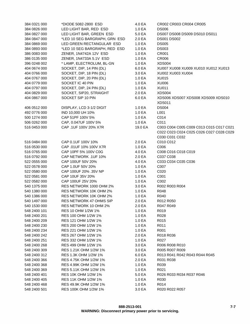
384 0321 000 *DIODE 5082-2800 ESD 4.0 EA CR002 CR003 CR004 CR005384 0826 000 LED LIGHT BAR, RED ESD 1.0 EA DS006384 0827 000 LED LIGHT BAR, GREEN ESD 5.0 EA DS007 DS008 DS009 DS010 DS011384 0847 000 *LED 10 SEG BARGRAPH, GRN ESD 2.0 EA DS001 DS002384 0869 000 LED GREEN RECTANGULAR ESD 1.0 EA DS005384 0893 000 *LED 10 SEG BARGRAPH, RED ESD 1.0 EA DS003386 0083 000 ZENER, 1N4742A 12V ESD 1.0 EA CR001386 0135 000 ZENER, 1N4733A 5.1V ESD 1.0 EA CR006396 0248 002 * LAMP, ELECTROLUM, BL-GN 1.0 EA XDS004404 0674 000 SOCKET, DIP, 14 PIN (DL) 6.0 EA XU007 XU008 XU009 XU010 XU012 XU013404 0766 000 SOCKET, DIP, 18 PIN (DL) 3.0 EA XU002 XU003 XU004404 0767 000 SOCKET, DIP, 20 PIN (DL) 1.0 EA XU015404 0779 000 SOCKET IC 40 PIN 1.0 EA XU006404 0797 000 SOCKET, DIP, 24 PIN (DL) 1.0 EA XU011404 0829 000 SOCKET, SIP20, STRAIGHT 2.0 EA XDS004404 0867 000 SOCKET SIP 10 PIN 6.0 EA XDS006 XDS007 XDS008 XDS009 XDS010
XDS011406 0512 000 DISPLAY, LCD 3-1/2 DIGIT 1.0 EA DS004492 0776 000 IND 10,000 UH 10% 1.0 EA L001500 1274 000 CAP 51PF 100V 5% 1.0 EA C014506 0262 000 CAP, 0.047UF 100V 5% 1.0 EA C011516 0453 000 CAP .1UF 100V 20% X7R 19.0 EA C003 C004 C005 C009 C013 C015 C017 C021
C022 C023 C024 C025 C026 C027 C028 C029C030 C031 C032
516 0484 000 CAP 0.1UF 100V 10% 2.0 EA C010 C012516 0530 000 CAP .01UF 10% 100V X7R 1.0 EA C006516 0765 000 CAP 10PF 5% 100V C0G 4.0 EA C008 C016 C018 C019516 0792 000 CAP NETWORK .1UF 10% 2.0 EA C037 C038522 0555 000 CAP 100UF 50V 20% 4.0 EA C033 C034 C035 C036522 0578 000 CAP 1.0UF 50V 20% 1.0 EA C007522 0580 000 CAP 100UF 20% .35V NP 1.0 EA C020522 0581 000 CAP 10UF 35V 20% 1.0 EA C001522 0582 000 CAP 100UF 25V 20% 1.0 EA C002540 1375 000 RES NETWORK 1000 OHM 2% 3.0 EA R002 R003 R004540 1380 000 RES NETWORK 10K OHM 2% 1.0 EA R048540 1386 000 RES NETWORK 10K OHM 2% 1.0 EA R040540 1497 000 RES NETWORK 47 OHMS SIP 2.0 EA R012 R050540 1530 000 RES NETWORK 10 OHM 2% 2.0 EA R047 R049548 2400 101 RES 10 OHM 1/2W 1% 1.0 EA R019548 2400 201 RES 100 OHM 1/2W 1% 1.0 EA R028548 2400 209 RES 121 OHM 1/2W 1% 1.0 EA R015548 2400 230 RES 200 OHM 1/2W 1% 1.0 EA R011548 2400 234 RES 221 OHM 1/2W 1% 1.0 EA R001548 2400 242 RES 267 OHM 1/2W 1% 2.0 EA R018 R036548 2400 251 RES 332 OHM 1/2W 1% 1.0 EA R027548 2400 268 RES 499 OHM 1/2W 1% 3.0 EA R006 R008 R010548 2400 309 RES 1.21K OHM 1/2W 1% 3.0 EA R005 R007 R009548 2400 312 RES 1.3K OHM 1/2W 1% 6.0 EA R013 R041 R042 R043 R044 R045548 2400 366 RES 4.75K OHM 1/2W 1% 2.0 EA R031 R038548 2400 368 RES 4.99K OHM 1/2W 1% 1.0 EA R039548 2400 369 RES 5.11K OHM 1/2W 1% 1.0 EA R021548 2400 401 RES 10K OHM 1/2W 1% 5.0 EA R026 R033 R034 R037 R046548 2400 405 RES 11K OHM 1/2W 1% 1.0 EA R030548 2400 468 RES 49.9K OHM 1/2W 1% 1.0 EA R014548 2400 501 RES 100K OHM 1/2W 1% 3.0 EA R020 R022 R057
888-2513-001 7-7WARNING: Disconnect primary power prior to servicing.

548 2400 513 RES 133K OHM 1/2W 1% 1.0 EA R051548 2400 526 RES 182K OHM 1/2W 1% 1.0 EA R024548 2400 530 RES 200K OHM 1/2W 1% 1.0 EA R032548 2400 532 RES 210K OHM 1/2W 1% 1.0 EA R023548 2400 601 RES 1MEG OHM 1/2W 1% 1.0 EA R035548 2400 626 RES 1.82MEG OHM 1/2W 1% 1.0 EA R025548 2400 669 RES 5.11MEG OHM 1/2W 1% 1.0 EA R016550 0947 000 TRIMPOT 1K OHM 1/2W 10% 1.0 EA R017550 0959 000 TRIMPOT 20K OHM 1/2W 10% 1.0 EA R029566 0015 002 * INVERTER, DC TO AC 1.0 EA U001604 1111 000 SW PB GRAY MOM W/O LED 4.0 EA S001 S002 S003 S004604 1119 000 SW PB RED MOM W/O LED 1.0 EA S010604 1121 000 SW PB BLUE MOM W/O LED 2.0 EA S008 S009604 1152 000 SW PB GRN MOM W/O LED 3.0 EA S005 S006 S007610 1043 000 *HDR 40C VERT 2ROW TOP LATCH 1.0 EA J001646 1301 201 LABEL, DANGER HI VOLTAGE 1.0 EA843 5458 281 SCH, XMTR DISPLAY BD. 0.0 EA843 5458 283 PWB, XMTR CONTROL BD. 1.0 EA917 2205 034 FOAM, “LCD” SPACER 1.0 EA XDS004917 2413 111 FIRMWARE, METER PAL 1.0 EA
Table 7-7. BD, LV POWER SUPPLY - 992 9067 001Harris PN Description QTY UM Reference Designators (U)354 0309 000 TERM SOLDER 3.0 EA TP007 TP008 TP009358 1928 000 JUMPER 1/4 LG 1/8H 6.0 EA JP005 JP006 JP007 JP008 JP009 JP010358 3475 000 STANDOFF 6-32 x 1/2 24.0 EA380 0125 000 XSTR, NPN 2N4401 ESD 1.0 EA Q002380 0189 000 XSTR, NPN 2N3904 ESD 1.0 EA Q001382 0770 000 IC, 74HC04 ESD 1.0 EA U012382 0882 000 IC, 78L05A ESD 1.0 EA U014382 1349 000 IC 74HC03 CMOS ESD 2.0 EA U005 U008382 1446 000 IC, MAX8216 ESD 2.0 EA U010 U011382 1451 000 IC, MAX933 ESD 2.0 EA U003 U004382 1467 000 IC MAX791CPE ESD 1.0 EA U007384 0431 000 RECT. 1N4001 ESD 11.0 EA CR001 CR002 CR003 CR004 CR005 CR006
CR011 CR018 CR020 CR021 CR022384 0661 000 LED, GRN, T 1-3/4, RT ANG ESD 5.0 EA DS004 DS005 DS006 DS007 DS009384 0662 000 LED RED ESD 2.0 EA DS003 DS008384 0664 000 LED YELLOW ESD 2.0 EA DS001 DS002384 0719 000 TRANSZORB 1N6373 5V 5W ESD 1.0 EA CR007384 0736 000 RECT,HIGH CURRENT GI/MR751 ESD 4.0 EA CR014 CR015 CR017 CR019384 0838 000 TRANSZORB 1N6380 36V 5W ESD 1.0 EA CR023386 0078 000 ZENER, 1N4734A 5.6V ESD 2.0 EA CR008 CR009386 0082 000 ZENER, 1N4744A 15V 1W 5% ESD 4.0 EA CR010 CR012 CR013 CR016398 0502 000 FUSE, FAST CART 5A 125V 5.0 EA F001 F004 F005 F006 F007398 0503 000 FUSE, FAST CART 3A 250V 3.0 EA F008 F009 F010402 0198 000 CLIP, FUSE 5MM DIA FUSE 16.0 EA 2/XF001 2/XF004 2/XF005 2/XF006 2/XF007
2/XF008 2/XF009 2/XF010404 0673 000 SOCKET, DIP, 8 PIN (DL) 2.0 EA XU003 XU004404 0674 000 SOCKET, DIP, 14 PIN (DL) 5.0 EA XU005 XU008 XU010 XU011 XU012404 0675 000 SOCKET, DIP, 16 PIN (DL) 1.0 EA XU007404 0821 000 SOCKET, DIP, 28 PIN (DL) 1.0 EA XK001404 0878 000 HEAT SINK 0.9" HIGH 1.0 EA U013404 0879 000 HEAT SINK 0.9" HIGH, FOR 3.0 EA U001 U002 U006
7-8 888-2513-001WARNING: Disconnect primary power prior to servicing.
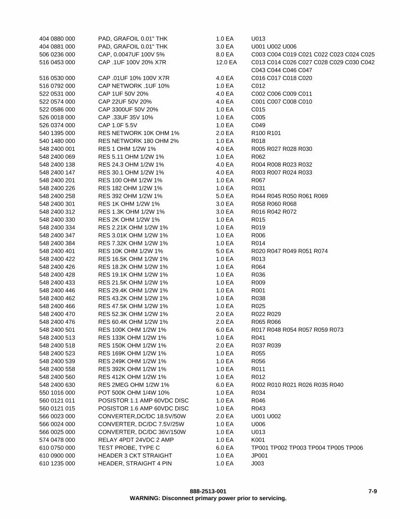
404 0880 000 PAD, GRAFOIL 0.01" THK 1.0 EA U013404 0881 000 PAD, GRAFOIL 0.01" THK 3.0 EA U001 U002 U006506 0236 000 CAP, 0.0047UF 100V 5% 8.0 EA C003 C004 C019 C021 C022 C023 C024 C025516 0453 000 CAP .1UF 100V 20% X7R 12.0 EA C013 C014 C026 C027 C028 C029 C030 C042
C043 C044 C046 C047516 0530 000 CAP .01UF 10% 100V X7R 4.0 EA C016 C017 C018 C020516 0792 000 CAP NETWORK .1UF 10% 1.0 EA C012522 0531 000 CAP 1UF 50V 20% 4.0 EA C002 C006 C009 C011522 0574 000 CAP 22UF 50V 20% 4.0 EA C001 C007 C008 C010522 0586 000 CAP 3300UF 50V 20% 1.0 EA C015526 0018 000 CAP .33UF 35V 10% 1.0 EA C005526 0374 000 CAP 1.0F 5.5V 1.0 EA C049540 1395 000 RES NETWORK 10K OHM 1% 2.0 EA R100 R101540 1480 000 RES NETWORK 180 OHM 2% 1.0 EA R018548 2400 001 RES 1 OHM 1/2W 1% 4.0 EA R005 R027 R028 R030548 2400 069 RES 5.11 OHM 1/2W 1% 1.0 EA R062548 2400 138 RES 24.3 OHM 1/2W 1% 4.0 EA R004 R008 R023 R032548 2400 147 RES 30.1 OHM 1/2W 1% 4.0 EA R003 R007 R024 R033548 2400 201 RES 100 OHM 1/2W 1% 1.0 EA R067548 2400 226 RES 182 OHM 1/2W 1% 1.0 EA R031548 2400 258 RES 392 OHM 1/2W 1% 5.0 EA R044 R045 R050 R061 R069548 2400 301 RES 1K OHM 1/2W 1% 3.0 EA R058 R060 R068548 2400 312 RES 1.3K OHM 1/2W 1% 3.0 EA R016 R042 R072548 2400 330 RES 2K OHM 1/2W 1% 1.0 EA R015548 2400 334 RES 2.21K OHM 1/2W 1% 1.0 EA R019548 2400 347 RES 3.01K OHM 1/2W 1% 1.0 EA R006548 2400 384 RES 7.32K OHM 1/2W 1% 1.0 EA R014548 2400 401 RES 10K OHM 1/2W 1% 5.0 EA R020 R047 R049 R051 R074548 2400 422 RES 16.5K OHM 1/2W 1% 1.0 EA R013548 2400 426 RES 18.2K OHM 1/2W 1% 1.0 EA R064548 2400 428 RES 19.1K OHM 1/2W 1% 1.0 EA R036548 2400 433 RES 21.5K OHM 1/2W 1% 1.0 EA R009548 2400 446 RES 29.4K OHM 1/2W 1% 1.0 EA R001548 2400 462 RES 43.2K OHM 1/2W 1% 1.0 EA R038548 2400 466 RES 47.5K OHM 1/2W 1% 1.0 EA R025548 2400 470 RES 52.3K OHM 1/2W 1% 2.0 EA R022 R029548 2400 476 RES 60.4K OHM 1/2W 1% 2.0 EA R065 R066548 2400 501 RES 100K OHM 1/2W 1% 6.0 EA R017 R048 R054 R057 R059 R073548 2400 513 RES 133K OHM 1/2W 1% 1.0 EA R041548 2400 518 RES 150K OHM 1/2W 1% 2.0 EA R037 R039548 2400 523 RES 169K OHM 1/2W 1% 1.0 EA R055548 2400 539 RES 249K OHM 1/2W 1% 1.0 EA R056548 2400 558 RES 392K OHM 1/2W 1% 1.0 EA R011548 2400 560 RES 412K OHM 1/2W 1% 1.0 EA R012548 2400 630 RES 2MEG OHM 1/2W 1% 6.0 EA R002 R010 R021 R026 R035 R040550 1016 000 POT 500K OHM 1/4W 10% 1.0 EA R034560 0121 011 POSISTOR 1.1 AMP 60VDC DISC 1.0 EA R046560 0121 015 POSISTOR 1.6 AMP 60VDC DISC 1.0 EA R043566 0023 000 CONVERTER,DC/DC 18.5V/50W 2.0 EA U001 U002566 0024 000 CONVERTER, DC/DC 7.5V/25W 1.0 EA U006566 0025 000 CONVERTER, DC/DC 36V/150W 1.0 EA U013574 0478 000 RELAY 4PDT 24VDC 2 AMP 1.0 EA K001610 0750 000 TEST PROBE, TYPE C 6.0 EA TP001 TP002 TP003 TP004 TP005 TP006610 0900 000 HEADER 3 CKT STRAIGHT 1.0 EA JP001610 1235 000 HEADER, STRAIGHT 4 PIN 1.0 EA J003
888-2513-001 7-9WARNING: Disconnect primary power prior to servicing.

610 1236 000 HEADER, STRAIGHT 8 PIN 1.0 EA J002610 1245 000 HEADER, STRAIGHT 24 PIN 1.0 EA J001612 1184 000 SHUNT JUMPER 0.1" CENTERS 1.0 EA JP001843 5458 291 SCH, LV POWER SUPPLY BD 0.0 EA843 5458 293 PWB, LV POWER SUPPLY BD 1.0 EA999 2830 001 HARDWARE LIST, LV POWER 1.0 EA
Table 7-8. PWA, XMTR DIGITAL I/O, 2-WAY - 992 9233 020Harris PN Description QTY UM Reference Designators (E)302 0016 000 SCR, 2-56 X 1/2 4.0 EA J001 AND J002306 0001 000 NUT, HEX 2-56 4.0 EA J001 AND J002310 0036 000 WASHER, FLAT .097 ID 8.0 EA J001 AND J002314 0001 000 WASHER, SPLIT-LOCK 2 4.0 EA J001 AND J002354 0309 000 TERM SOLDER 5.0 EA TP001 TP002 TP003 TP004 TP005358 1928 000 JUMPER 1/4 LG 1/8H 3.0 EA JP004 JP005 JP007382 0784 000 IC, 74HC85 ESD 2.0 EA U005 U006382 1045 000 IC, 74HC541 ESD 2.0 EA U002 U004382 1097 000 IC, 74HCT05 ESD 1.0 EA U007384 0662 000 LED RED ESD 1.0 EA DS001384 0719 000 TRANSZORB 1N6373 5V 5W ESD 1.0 EA CR001384 0720 000 TRANSZORB 1N6377 15V 5W ESD 2.0 EA CR002 CR003384 0838 000 TRANSZORB 1N6380 36V 5W ESD 1.0 EA CR004404 0674 000 SOCKET, DIP, 14 PIN (DL) 1.0 EA XU007404 0675 000 SOCKET, DIP, 16 PIN (DL) 2.0 EA XU005 XU006404 0767 000 SOCKET, DIP, 20 PIN (DL) 2.0 EA XU002 XU004404 0836 000 SOCKET, PLCC-84, THROUGH HOLE 2.0 EA XU001 XU003516 0453 000 CAP .1UF 100V 20% X7R 13.0 EA C001 C002 C003 C004 C005 C006 C007 C008
C009 C010 C011 C012 C013516 0813 000 NTWK, CAP .01UF 50V 20% SIP 7.0 EA C014 C015 C016 C017 C018 C019 C020540 1366 000 RES NETWORK 100 OHM 2% 7.0 EA R012 R013 R014 R015 R016 R017 R018540 1386 000 RES NETWORK 10K OHM 2% 9.0 EA R001 R002 R003 R004 R005 R006 R008 R009
R010540 1392 000 RES NETWORK 4700 OHM 2% 1.0 EA R007548 2400 258 RES 392 OHM 1/2W 1% 1.0 EA R011610 1168 000 CONN, BACKPLANE, RT ANGLE 64C 1.0 EA J002610 1273 000 PLUG, 96 CONTACT MALE RT 1.0 EA J001843 5458 181 SCH, DIGITAL I/O 0.0 EA843 5458 183 PWB, DIGITAL I/O 1.0 EA917 2413 119 FIRMWARE, DIGITAL I/O #1 1.0 EA917 2413 120 FIRMWARE, DIGITAL I/O #2 1.0 EA
Table 7-9. PWA, CUSTOMER INTERFACE, 2-WAY - 992 9237 020Harris PN Description QTY UM Reference Designators (F)302 0016 000 SCR, 2-56 X 1/2 4.0 EA J001 AND J002306 0001 000 NUT, HEX 2-56 4.0 EA J001 AND J002310 0036 000 WASHER, FLAT .097 ID 8.0 EA J001 AND J002314 0001 000 WASHER, SPLIT-LOCK 2 4.0 EA J001 AND J002354 0309 000 TERM SOLDER 7.0 EA TP001 TP002 TP003 TP004 TP005 TP006
TP007358 1928 000 JUMPER 1/4 LG 1/8H 7.0 EA JP002 JP003 JP004 JP005 JP006 JP009
JP010380 0126 000 XSTR, PNP 2N4403 ESD 1.0 EA Q001
7-10 888-2513-001WARNING: Disconnect primary power prior to servicing.
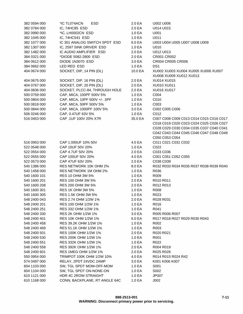
382 0594 000 *IC TL074ACN ESD 2.0 EA U002 U006382 0784 000 IC, 74HC85 ESD 2.0 EA U014 U015382 0990 000 *IC, LH0002CN ESD 1.0 EA U001382 1045 000 IC, 74HC541 ESD 1.0 EA U011382 1077 000 IC 301 ANALOG SWITCH SPDT ESD 6.0 EA U003 U004 U005 U007 U008 U009382 1307 000 IC, 2597 SINK DRIVER ESD 1.0 EA U010382 1482 000 IC AUDIO AMPLIFIER ESD 2.0 EA U012 U013384 0321 000 *DIODE 5082-2800 ESD 2.0 EA CR001 CR002384 0612 000 DIODE 1N3070 ESD 3.0 EA CR004 CR005 CR006384 0662 000 LED RED ESD 1.0 EA DS1404 0674 000 SOCKET, DIP, 14 PIN (DL) 10.0 EA XU002 XU003 XU004 XU005 XU006 XU007
XU008 XU009 XU012 XU013404 0675 000 SOCKET, DIP, 16 PIN (DL) 2.0 EA XU014 XU015404 0767 000 SOCKET, DIP, 20 PIN (DL) 2.0 EA XU010 XU011404 0836 000 SOCKET, PLCC-84, THROUGH HOLE 2.0 EA XU016 XU017500 0759 000 CAP, MICA, 100PF 500V 5% 1.0 EA C004500 0804 000 CAP, MICA, 10PF 500V +/- .5PF 1.0 EA C010500 0818 000 CAP, MICA, 50PF 500V 5% 1.0 EA C003500 0844 000 CAP, MICA, 1000PF 100V 5% 3.0 EA C002 C005 C006506 0246 000 CAP, 0.47UF 63V 5% 1.0 EA C012516 0453 000 CAP .1UF 100V 20% X7R 35.0 EA C007 C008 C009 C013 C014 C015 C016 C017
C018 C019 C020 C023 C024 C025 C026 C027C028 C029 C030 C034 C035 C037 C040 C041C042 C043 C044 C045 C046 C047 C048 C049C050 C053 C054
516 0953 000 CAP 1.000UF 10% 50V 4.0 EA C011 C021 C031 C032522 0548 000 CAP 10UF 50V 20% 1.0 EA C022522 0554 000 CAP 4.7UF 50V 20% 2.0 EA C033 C036522 0555 000 CAP 100UF 50V 20% 4.0 EA C001 C051 C052 C055522 0573 000 CAP 47UF 63V 20% 2.0 EA C038 C039540 1386 000 RES NETWORK 10K OHM 2% 8.0 EA R032 R033 R034 R035 R037 R038 R039 R040540 1458 000 RES NETWORK 1M OHM 2% 1.0 EA R036540 1600 101 RES 10 OHM 3W 5% 1.0 EA R009540 1600 201 RES 100 OHM 3W 5% 2.0 EA R010 R011540 1600 208 RES 200 OHM 3W 5% 2.0 EA R012 R013540 1600 301 RES 1K OHM 3W 5% 1.0 EA R008540 1600 305 RES 1.5K OHM 3W 5% 1.0 EA R023548 2400 043 RES 2.74 OHM 1/2W 1% 2.0 EA R028 R031548 2400 201 RES 100 OHM 1/2W 1% 1.0 EA R016548 2400 251 RES 332 OHM 1/2W 1% 1.0 EA R041548 2400 330 RES 2K OHM 1/2W 1% 3.0 EA R005 R006 R007548 2400 401 RES 10K OHM 1/2W 1% 6.0 EA R017 R018 R027 R029 R030 R043548 2400 458 RES 39.2K OHM 1/2W 1% 1.0 EA R002548 2400 469 RES 51.1K OHM 1/2W 1% 1.0 EA R003548 2400 501 RES 100K OHM 1/2W 1% 2.0 EA R020 R021548 2400 530 RES 200K OHM 1/2W 1% 1.0 EA R001548 2400 551 RES 332K OHM 1/2W 1% 1.0 EA R022548 2400 558 RES 392K OHM 1/2W 1% 2.0 EA R004 R019548 2400 601 RES 1MEG OHM 1/2W 1% 2.0 EA R025 R026550 0954 000 TRIMPOT 100K OHM 1/2W 10% 4.0 EA R014 R015 R024 R42574 0497 000 RELAY, 2PDT 24VDC 2AMP 3.0 EA K001 K006 K007604 1103 000 SW, TGL SPDT MOM-OFF-MOM 1.0 EA S001604 1104 000 SW, TGL SPDT ON-NONE-ON 1.0 EA S002610 1121 000 HDR 4C 2ROW STRAIGHT 1.0 EA JP007610 1168 000 CONN, BACKPLANE, RT ANGLE 64C 1.0 EA J002
888-2513-001 7-11WARNING: Disconnect primary power prior to servicing.

610 1273 000 PLUG, 96 CONTACT MALE RT 1.0 EA J001612 1184 000 SHUNT JUMPER 0.1" CENTERS 1.0 EA XJP007612 1476 000 JACK, HEADPHONE STEREO 1.0 EA J003670 0045 000 LDR VTL5C4 1.0 EA CR003843 5458 221 SCH, CUSTOMER INTERFACE 0.0 EA843 5458 223 PWB, CUSTOMER INTERFACE 1.0 EA917 2413 123 FIRMWARE, CUSTOMER 1.0 EA917 2413 124 FIRMWARE, MONITOR 1.0 EA929 9009 216 XFMR 1.0 EA T001
Table 7-10. PWA, XMTR CONTROL, 2-WAY - 992 9245 020Harris PN Description QTY UM Reference Designators (E)302 0016 000 SCR, 2-56 X 1/2 4.0 EA J001 AND J002306 0001 000 NUT, HEX 2-56 4.0 EA J001 AND J002310 0036 000 WASHER, FLAT .097 ID 8.0 EA J001 AND J002314 0001 000 WASHER, SPLIT-LOCK 2 4.0 EA J001 AND J002354 0309 000 TERM SOLDER 4.0 EA TP001 TP002 TP003 TP004358 1928 000 JUMPER 1/4 LG 1/8H 6.0 EA JP004 JP005 JP006 JP007 JP009 JP014382 0260 000 IC, 555 ESD 1.0 EA U010382 0770 000 IC, 74HC04 ESD 1.0 EA U004382 0784 000 IC, 74HC85 ESD 1.0 EA U015382 0800 000 IC, 74HC161 ESD 5.0 EA U009 U011 U012 U013 U014382 0812 000 IC 74HC221 ESD 1.0 EA U003382 1045 000 IC, 74HC541 ESD 5.0 EA U001 U002 U006 U007 U016384 0662 000 LED RED ESD 1.0 EA DS001404 0673 000 SOCKET, DIP, 8 PIN (DL) 1.0 EA XU010404 0674 000 SOCKET, DIP, 14 PIN (DL) 1.0 EA XU004404 0675 000 SOCKET, DIP, 16 PIN (DL) 7.0 EA XU003 XU009 XU011 XU012 XU013 XU014
XU015404 0767 000 SOCKET, DIP, 20 PIN (DL) 5.0 EA XU001 XU002 XU006 XU007 XU016404 0836 000 SOCKET, PLCC-84, THROUGH HOLE 2.0 EA XU005 XU008516 0453 000 CAP .1UF 100V 20% X7R 23.0 EA C003 C005 C006 C007 C008 C009 C010 C011
C012 C013 C014 C017 C018 C019 C020 C021C022 C023 C024 C025 C026 C027 C028
516 0530 000 CAP .01UF 10% 100V X7R 1.0 EA C004522 0548 000 CAP 10UF 50V 20% 2.0 EA C001 C002522 0555 000 CAP 100UF 50V 20% 2.0 EA C015 C016540 1386 000 RES NETWORK 10K OHM 2% 4.0 EA R001 R003 R010 R011540 1493 000 RES NETWORK 100K OHM 1.0 EA R002548 2400 258 RES 392 OHM 1/2W 1% 1.0 EA R007548 2400 264 RES 453 OHM 1/2W 1% 1.0 EA548 2400 301 RES 1K OHM 1/2W 1% 1.0 EA R004548 2400 466 RES 47.5K OHM 1/2W 1% 2.0 EA R005 R006604 0469 000 SW TGL SPDT 1.0 EA S002604 0935 000 SW, PB SINGLE SECT 1.0 EA S001610 1168 000 CONN, BACKPLANE, RT ANGLE 64C 1.0 EA J002610 1273 000 PLUG, 96 CONTACT MALE RT 1.0 EA J001843 5450 651 CHART, CONTROLLER FUNCTION 0.0 EA843 5458 103 PWB, COMBINER CONTROL 1.0 EA843 5458 311 SCH, CONTROL BD,XMTR CTRL 0.0 EA917 2413 117 FIRMWARE, XMTR BUS CTLR 1.0 EA917 2413 118 FIRMWARE, I/O XMTR CTLR UNIT 1.0 EA
7-12 888-2513-001WARNING: Disconnect primary power prior to servicing.

Table 7-11. PWA, EXTENDER CARD - 992 9247 001Harris PN Description QTY UM Reference Designators (G)302 0016 000 SCR, 2-56 X 1/2 8.0 EA J001, J002, P001, P002306 0001 000 NUT, HEX 2-56 8.0 EA J001, J002, P001, P002310 0036 000 WASHER, FLAT .097 ID 16.0 EA J001, J002, P001, P002314 0001 000 WASHER, SPLIT-LOCK 2 8.0 EA J001, J002, P001, P002610 1273 000 PLUG, 96 CONTACT MALE RT 2.0 EA J001 J002612 1481 000 RECEPTACLE, 96 PIN FEMALE 2.0 EA P001 P002843 5458 301 SCH, EXTENDER CARD 0.0 EA843 5458 303 PWB, EXTENDER CARD 1.0 EA
Table 7-12. PWA AUDIO CONTROL - 992 9511 313Harris PN Description QTY UM Reference Designators (G)055 0100 005 *THERMAL COMPOUND, 8OZ JAR 0.0 EA XU40. XU41300 1485 000 SCR, 4-40 X 5/16 2.0 EA #XU40 #XU41302 0016 000 SCR, 2-56 X 1/2 4.0 EA J1 AND J2304 0087 000 NUT, HEX 4-40 2.0 EA #XU40 #XU41306 0001 000 NUT, HEX 2-56 4.0 EA J1 AND J2308 0003 000 NO 4 FLAT WASHER BRS 2.0 EA #XU40 #XU41310 0036 000 WASHER, FLAT .097 ID 8.0 EA J1 AND J2312 0045 000 WASHER, SPLIT-LOCK 4 2.0 EA #XU40 #XU41314 0001 000 WASHER, SPLIT-LOCK 2 4.0 EA J1 AND J2354 0309 000 TERM SOLDER 22.0 EA TP3 TP4 TP5 TP9 TP10 TP11 TP12 TP13
TP14 TP15 TP16 TP17 TP18 TP19 TP20 TP21TP22 TP23 TP24 TP25 TP26 TP27
358 1928 000 JUMPER 1/4 LG 1/8H 14.0 EA JP2 JP3 JP4 JP8 JP9 JP10 JP12 JP13 JP14JP15 JP18 JP19 JP20 JP23
382 0371 000 IC, MC7912CT ESD 1.0 EA U40382 0406 000 IC, MC7812CT ESD 1.0 EA U41382 0594 001 *IC TL074ACN ESD 1.0 EA U11382 0648 000 IC, LM339A ESD 5.0 EA U26 U27 U28 U29 U30382 0749 000 IC NE5532A ESD 6.0 EA U13 U14 U18 U19 U23 U24382 0770 000 IC, 74HC04 ESD 1.0 EA U33382 0784 000 IC, 74HC85 ESD 2.0 EA U31 U35382 0812 000 IC 74HC221 ESD 1.0 EA U34382 1045 000 IC, 74HC541 ESD 1.0 EA U32382 1077 000 IC 301 ANALOG SWITCH SPDT ESD 7.0 EA U5 U15 U17 U20 U21 U22 U42382 1204 000 IC TC4423 ESD 1.0 EA U25382 1307 000 IC, 2597 SINK DRIVER ESD 1.0 EA U7382 1309 000 IC, MAX 378 8 CH MUX ESD 3.0 EA U1 U38 U39384 0205 000 DIODE SILICON 1N914/4148 ESD 1.0 EA CR17384 0431 000 RECT. 1N4001 ESD 3.0 EA CR16 CR18 CR19384 0661 000 LED, GRN, T 1-3/4, RT ANG ESD 3.0 EA DS5 DS6 DS7384 0662 000 LED RED ESD 1.0 EA DS1404 0513 000 HEAT SINK PA1-1CB 2.0 EA XU40 XU41404 0673 000 SOCKET, DIP, 8 PIN (DL) 7.0 EA XU13 XU14 XU18 XU19 XU23 XU24 XU25404 0836 000 SOCKET, PLCC-84, THROUGH HOLE 1.0 EA XU36492 0881 000 CHOKE, 10MH +/- 20% 4.0 EA L1 L2 L3 L4500 0818 000 CAP, MICA, 50PF 500V 5% 2.0 EA C6 C10516 0453 000 CAP .1UF 100V 20% X7R 55.0 EA
888-2513-001 7-13WARNING: Disconnect primary power prior to servicing.

C1 C3 C21 C22 C26 C31 C32 C39 C40 C41C42 C43 C44 C45 C46 C47 C48 C49 C50 C51C52 C53 C54 C55 C56 C57 C58 C59 C60 C61C62 C63 C64 C65 C66 C67 C68 C69 C70 C71C72 C73 C74 C78 C79 C80 C81 C82 C83 C84C85 C86 C87 C89 C93
516 0792 000 CAP NETWORK .1UF 10% 3.0 EA C75 C76 C77522 0524 000 CAP 10 UF 100V 20% NON-POLAR 2.0 EA C4 C11522 0555 000 CAP 100UF 50V 20% 4.0 EA C33 C91 C94 C95522 0588 000 CAP 100UF 25V 20% NP 1.0 EA C151526 0094 000 CAP 0.1UF 50V 10% 1.0 EA C90540 1380 000 RES NETWORK 10K OHM 2% 3.0 EA R70 R72 R73540 1383 000 RES NETWORK 100K OHM 2% 1.0 EA R87540 1386 000 RES NETWORK 10K OHM 2% 3.0 EA R77 R78 R81540 1458 000 RES NETWORK 1M OHM 2% 1.0 EA R86540 1459 000 RES NETWORK 300 OHM 2% 2.0 EA R71 R74540 1493 000 RES NETWORK 100K OHM 1.0 EA R76540 1548 000 RES NETWORK 1M OHM 2% 4.0 EA R69 R75 R82 R83548 2400 201 RES 100 OHM 1/2W 1% 4.0 EA R8 R10 R80 R88548 2400 254 RES 357 OHM 1/2W 1% 1.0 EA R134548 2400 258 RES 392 OHM 1/2W 1% 1.0 EA R79548 2400 289 RES 825 OHM 1/2W 1% 2.0 EA R135 R136548 2400 330 RES 2K OHM 1/2W 1% 1.0 EA R85548 2400 401 RES 10K OHM 1/2W 1% 3.0 EA R41 R42 R47548 2400 430 RES 20K OHM 1/2W 1% 4.0 EA R38 R45 R51 R84548 2400 466 RES 47.5K OHM 1/2W 1% 1.0 EA R89548 2400 601 RES 1MEG OHM 1/2W 1% 2.0 EA R67 R68548 2400 634 RES 2.21MEG OHM 1/2W 1% 3.0 EA R9 R90 R91550 0961 000 TRIMPOT 50K OHM 1/2W 10% 2.0 EA R16 R17574 0497 000 RELAY, 2PDT 24VDC 2AMP 6.0 EA K1 K2 K3 K4 K5 K6604 1103 000 SW, TGL SPDT MOM-OFF-MOM 1.0 EA S1610 0900 000 HEADER 3 CKT STRAIGHT 10.0 EA JP1 JP5 JP6 JP7 JP11 JP21 JP22 JP24 JP25
JP26610 1069 000 HEADER 9 PIN SINGLE ROW 1.0 EA J4610 1168 000 CONN, BACKPLANE, RT ANGLE 64C 2.0 EA J1 J2612 1184 000 SHUNT JUMPER 0.1" CENTERS 10.0 EA XJP1 XJP5 XJP6 XJP7 XJP11 XJP21 XJP22
XJP24 XJP25 XJP26620 2930 000 RECEPTACLE RT ANGLE BNC 1.0 EA J3917 2332 718 FIRMWARE, ACC+ 1.0 EA U9 U10917 2413 121 FIRMWARE, AUDIO CONTROL 1.0 EA U36917 2551 014 FIRMWARE, ACC DELAY 1.0 EA U16992 9511 314 PWA AUDIO CONTROL SMT 1.0 EA
Table 7-13. SUBRACK PLC - 992 9229 020Harris PN Description QTY UM Reference Designators (B)358 0737 000 SLIDES DRAWER 1.0 PR358 3490 000 END STOP, 264 TERM BLOCK 2.0 EA #TB001358 3491 000 END PLATE, 264 TERM BLOCK 1.0 EA #TB001384 0736 000 RECT,HIGH CURRENT GI/MR751 ESD 2.0 EA #TB001448 0224 000 HANDLE ALUM 1.0 EA614 0892 000 TERM BLOCK, 4C RAIL MNT 6.0 EA #TB001614 0896 000 TERM BLOCK, 4C GND 2.0 EA #TB001646 0973 000 *LABEL, 230V 1.0 EA #TOUCH SCREEN746 0176 000 *MONITOR, 10" STN COLOR 1.0 EA
7-14 888-2513-001WARNING: Disconnect primary power prior to servicing.

917 2413 341 CARRIER RAIL - 6.3" 1.0 EA #TB001922 1238 351 CABLE, RIBBON 1.0 EA TCU PLC J1 TO CCU PLC J1943 5450 568 FRONT PANEL 1.0 EA943 5450 585 PANEL, DIVIDER 2.0 EA943 5450 669 CABLE, PLC TO MMI 1.0 EA952 9195 040 CHASSIS 1.0 EA952 9195 060 CABLE, PLC SUBRACK AC 1.0 EA992 9241 020 PROGRAMMABLE LOGIC CONTROL 1.0 EA A001
Table 7-14. PROGRAMMABLE LOGIC CONTROL - 992 9241 020Harris PN Description QTY UM Reference Designators (B)382 1456 000 *IC, EEPROM 1747-M11 ESD 1.0 EA448 1015 000 RACK, 7 SLOT, 2.0 EA736 0267 000 POWER SUPPLY [email protected] 2.0 EA746 0168 000 MODULE, 32PT DISCRETE INPUT 2.0 EA746 0169 000 MODULE, 32PT DISCRETE OUTPUT 2.0 EA746 0170 000 MODULE, ANALOG INPUT 4 PT 1.0 EA746 0171 000 MODULE, ANALOG I/O 4 PT 1.0 EA746 0175 000 FILLERS,SLC 500 CARD SLOT 6.0 EA746 0179 000 MODULE,REMOTE I/O SCANNER 1.0 EA746 0182 000 *MODULE, SLC 5/04 CPU 1.0 EA
Table 7-15. SUBRACK, COMBINER CONTROL - 992 9230 002Harris PN Description QTY UM Reference Designators (J)254 0033 000 COND, FLEX .084 OD 1 FT296 0054 000 PLASTIC TUBE 8AWG, CLEAR 1 FT303 1205 012 SCREW, M5-0.8 X 12 CSK HD 4.0 EA303 1304 008 SCREW M4-0.7 X 8, SLOTTED 50.0 EA303 1305 012 SCREW,M5-0.8 X 12 SLOTTED 16.0 EA303 4125 008 SCREW, MACH M2.5 X 8 22.0 EA311 0011 025 WASHER, FLAT M2.5 22.0 EA315 0021 025 WASHER, SPLIT LOCK M2.5 22.0 EA315 0023 040 WASHER, EXT LOCK M4 50.0 EA315 0023 050 WASHER, EXT LOCK M5 16.0 EA448 0333 000 HANDLE, BLACK FINISH 1.0 EA448 1039 000 RAIL, FRONT HORIZONTAL, 2.0 EA448 1040 000 RAIL, HORIZONTAL REAR, 4.0 EA448 1042 000 INSERT, THREADED, M2.5 2.0 EA448 1043 000 SCREW,THREADED INSERT MTG 4.0 EA448 1044 000 STRIP, INSULATING 2.0 EA448 1045 000 CLIP,INSULATOR ATTACHMENT 6.0 EA448 1046 000 HANDLE, 2.0 EA448 1047 000 KIT, HINGE, 84HP 1.0 EA448 1048 000 RAIL, GUIDE, 280MM, 20.0 EA448 1049 000 FLANGE, 19INCH MOUNTING 2.0 EA448 1050 000 RETAINER, BOARD, BOTTOM, 10.0 EA448 1052 000 RAIL, CENTER WITH TWO 1.0 EA448 1059 000 FASTENER, QUICK-RELEASE 2.0 EA917 2413 511 CABLE EMERGENCY OFF 1.0 EA939 8154 332 PANEL, SIDE, SUBRACK 2.0 EA939 8154 333 PANEL, TOP, BOTTOM, 2.0 EA939 8154 357 SHIELD, FRONT, SUBRACK 1.0 EA
888-2513-001 7-15WARNING: Disconnect primary power prior to servicing.
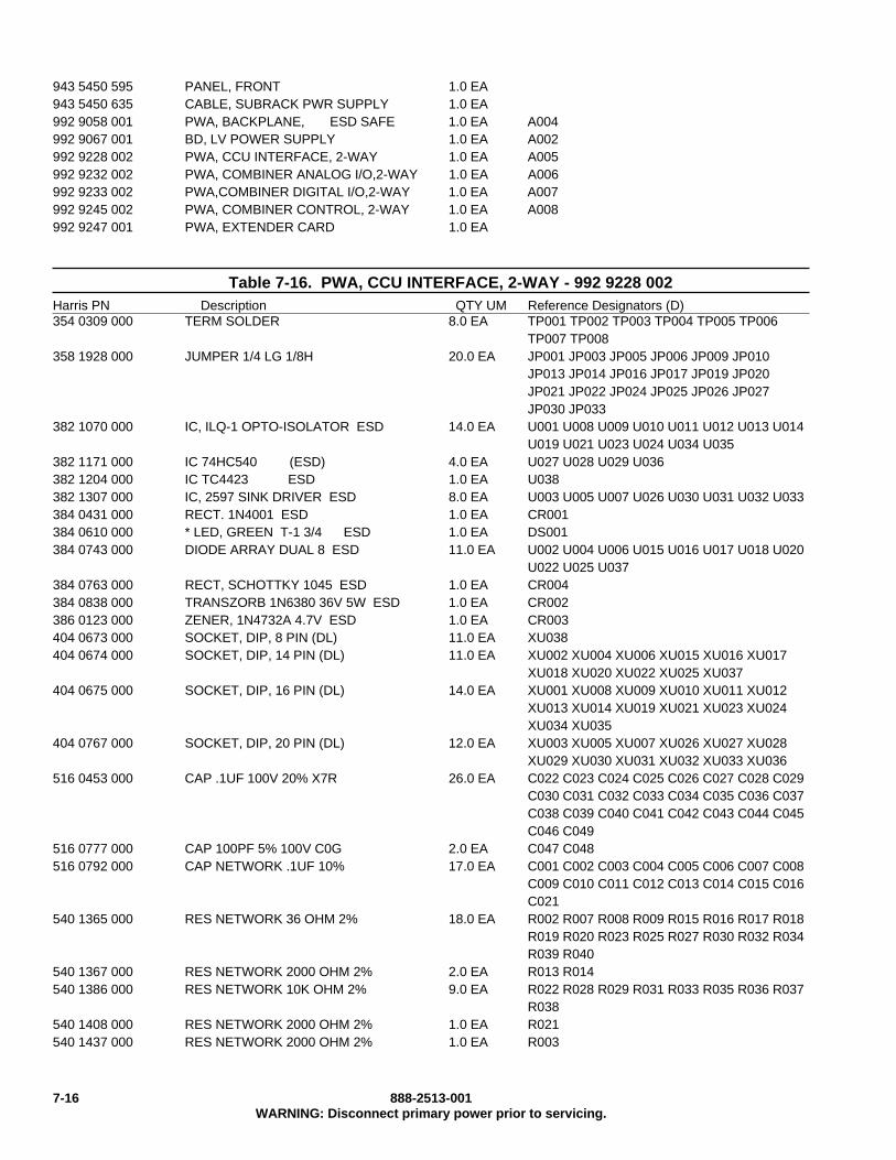
943 5450 595 PANEL, FRONT 1.0 EA943 5450 635 CABLE, SUBRACK PWR SUPPLY 1.0 EA992 9058 001 PWA, BACKPLANE, ESD SAFE 1.0 EA A004992 9067 001 BD, LV POWER SUPPLY 1.0 EA A002992 9228 002 PWA, CCU INTERFACE, 2-WAY 1.0 EA A005992 9232 002 PWA, COMBINER ANALOG I/O,2-WAY 1.0 EA A006992 9233 002 PWA,COMBINER DIGITAL I/O,2-WAY 1.0 EA A007992 9245 002 PWA, COMBINER CONTROL, 2-WAY 1.0 EA A008992 9247 001 PWA, EXTENDER CARD 1.0 EA
Table 7-16. PWA, CCU INTERFACE, 2-WAY - 992 9228 002Harris PN Description QTY UM Reference Designators (D)354 0309 000 TERM SOLDER 8.0 EA TP001 TP002 TP003 TP004 TP005 TP006
TP007 TP008358 1928 000 JUMPER 1/4 LG 1/8H 20.0 EA JP001 JP003 JP005 JP006 JP009 JP010
JP013 JP014 JP016 JP017 JP019 JP020JP021 JP022 JP024 JP025 JP026 JP027JP030 JP033
382 1070 000 IC, ILQ-1 OPTO-ISOLATOR ESD 14.0 EA U001 U008 U009 U010 U011 U012 U013 U014U019 U021 U023 U024 U034 U035
382 1171 000 IC 74HC540 (ESD) 4.0 EA U027 U028 U029 U036382 1204 000 IC TC4423 ESD 1.0 EA U038382 1307 000 IC, 2597 SINK DRIVER ESD 8.0 EA U003 U005 U007 U026 U030 U031 U032 U033384 0431 000 RECT. 1N4001 ESD 1.0 EA CR001384 0610 000 * LED, GREEN T-1 3/4 ESD 1.0 EA DS001384 0743 000 DIODE ARRAY DUAL 8 ESD 11.0 EA U002 U004 U006 U015 U016 U017 U018 U020
U022 U025 U037384 0763 000 RECT, SCHOTTKY 1045 ESD 1.0 EA CR004384 0838 000 TRANSZORB 1N6380 36V 5W ESD 1.0 EA CR002386 0123 000 ZENER, 1N4732A 4.7V ESD 1.0 EA CR003404 0673 000 SOCKET, DIP, 8 PIN (DL) 11.0 EA XU038404 0674 000 SOCKET, DIP, 14 PIN (DL) 11.0 EA XU002 XU004 XU006 XU015 XU016 XU017
XU018 XU020 XU022 XU025 XU037404 0675 000 SOCKET, DIP, 16 PIN (DL) 14.0 EA XU001 XU008 XU009 XU010 XU011 XU012
XU013 XU014 XU019 XU021 XU023 XU024XU034 XU035
404 0767 000 SOCKET, DIP, 20 PIN (DL) 12.0 EA XU003 XU005 XU007 XU026 XU027 XU028XU029 XU030 XU031 XU032 XU033 XU036
516 0453 000 CAP .1UF 100V 20% X7R 26.0 EA C022 C023 C024 C025 C026 C027 C028 C029C030 C031 C032 C033 C034 C035 C036 C037C038 C039 C040 C041 C042 C043 C044 C045C046 C049
516 0777 000 CAP 100PF 5% 100V C0G 2.0 EA C047 C048516 0792 000 CAP NETWORK .1UF 10% 17.0 EA C001 C002 C003 C004 C005 C006 C007 C008
C009 C010 C011 C012 C013 C014 C015 C016C021
540 1365 000 RES NETWORK 36 OHM 2% 18.0 EA R002 R007 R008 R009 R015 R016 R017 R018R019 R020 R023 R025 R027 R030 R032 R034R039 R040
540 1367 000 RES NETWORK 2000 OHM 2% 2.0 EA R013 R014540 1386 000 RES NETWORK 10K OHM 2% 9.0 EA R022 R028 R029 R031 R033 R035 R036 R037
R038540 1408 000 RES NETWORK 2000 OHM 2% 1.0 EA R021540 1437 000 RES NETWORK 2000 OHM 2% 1.0 EA R003
7-16 888-2513-001WARNING: Disconnect primary power prior to servicing.
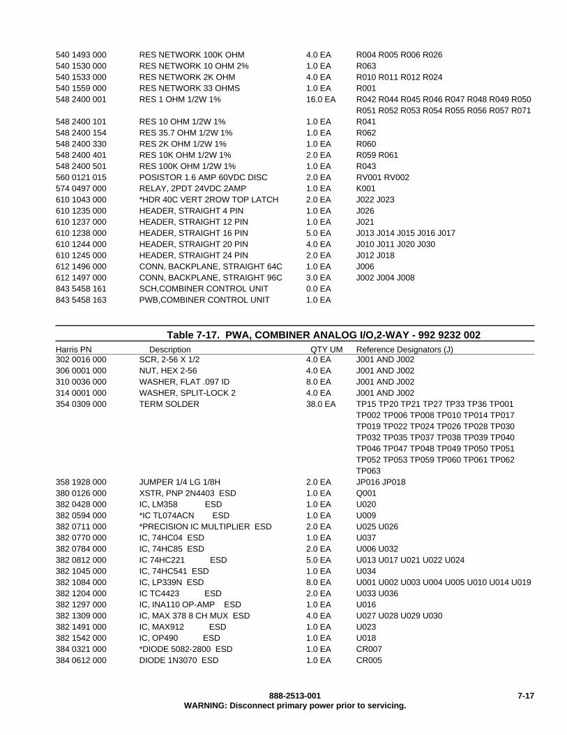
540 1493 000 RES NETWORK 100K OHM 4.0 EA R004 R005 R006 R026540 1530 000 RES NETWORK 10 OHM 2% 1.0 EA R063540 1533 000 RES NETWORK 2K OHM 4.0 EA R010 R011 R012 R024540 1559 000 RES NETWORK 33 OHMS 1.0 EA R001548 2400 001 RES 1 OHM 1/2W 1% 16.0 EA R042 R044 R045 R046 R047 R048 R049 R050
R051 R052 R053 R054 R055 R056 R057 R071548 2400 101 RES 10 OHM 1/2W 1% 1.0 EA R041548 2400 154 RES 35.7 OHM 1/2W 1% 1.0 EA R062548 2400 330 RES 2K OHM 1/2W 1% 1.0 EA R060548 2400 401 RES 10K OHM 1/2W 1% 2.0 EA R059 R061548 2400 501 RES 100K OHM 1/2W 1% 1.0 EA R043560 0121 015 POSISTOR 1.6 AMP 60VDC DISC 2.0 EA RV001 RV002574 0497 000 RELAY, 2PDT 24VDC 2AMP 1.0 EA K001610 1043 000 *HDR 40C VERT 2ROW TOP LATCH 2.0 EA J022 J023610 1235 000 HEADER, STRAIGHT 4 PIN 1.0 EA J026610 1237 000 HEADER, STRAIGHT 12 PIN 1.0 EA J021610 1238 000 HEADER, STRAIGHT 16 PIN 5.0 EA J013 J014 J015 J016 J017610 1244 000 HEADER, STRAIGHT 20 PIN 4.0 EA J010 J011 J020 J030610 1245 000 HEADER, STRAIGHT 24 PIN 2.0 EA J012 J018612 1496 000 CONN, BACKPLANE, STRAIGHT 64C 1.0 EA J006612 1497 000 CONN, BACKPLANE, STRAIGHT 96C 3.0 EA J002 J004 J008843 5458 161 SCH,COMBINER CONTROL UNIT 0.0 EA843 5458 163 PWB,COMBINER CONTROL UNIT 1.0 EA
Table 7-17. PWA, COMBINER ANALOG I/O,2-WAY - 992 9232 002Harris PN Description QTY UM Reference Designators (J)302 0016 000 SCR, 2-56 X 1/2 4.0 EA J001 AND J002306 0001 000 NUT, HEX 2-56 4.0 EA J001 AND J002310 0036 000 WASHER, FLAT .097 ID 8.0 EA J001 AND J002314 0001 000 WASHER, SPLIT-LOCK 2 4.0 EA J001 AND J002354 0309 000 TERM SOLDER 38.0 EA TP15 TP20 TP21 TP27 TP33 TP36 TP001
TP002 TP006 TP008 TP010 TP014 TP017TP019 TP022 TP024 TP026 TP028 TP030TP032 TP035 TP037 TP038 TP039 TP040TP046 TP047 TP048 TP049 TP050 TP051TP052 TP053 TP059 TP060 TP061 TP062TP063
358 1928 000 JUMPER 1/4 LG 1/8H 2.0 EA JP016 JP018380 0126 000 XSTR, PNP 2N4403 ESD 1.0 EA Q001382 0428 000 IC, LM358 ESD 1.0 EA U020382 0594 000 *IC TL074ACN ESD 1.0 EA U009382 0711 000 *PRECISION IC MULTIPLIER ESD 2.0 EA U025 U026382 0770 000 IC, 74HC04 ESD 1.0 EA U037382 0784 000 IC, 74HC85 ESD 2.0 EA U006 U032382 0812 000 IC 74HC221 ESD 5.0 EA U013 U017 U021 U022 U024382 1045 000 IC, 74HC541 ESD 1.0 EA U034382 1084 000 IC, LP339N ESD 8.0 EA U001 U002 U003 U004 U005 U010 U014 U019382 1204 000 IC TC4423 ESD 2.0 EA U033 U036382 1297 000 IC, INA110 OP-AMP ESD 1.0 EA U016382 1309 000 IC, MAX 378 8 CH MUX ESD 4.0 EA U027 U028 U029 U030382 1491 000 IC, MAX912 ESD 1.0 EA U023382 1542 000 IC, OP490 ESD 1.0 EA U018384 0321 000 *DIODE 5082-2800 ESD 1.0 EA CR007384 0612 000 DIODE 1N3070 ESD 1.0 EA CR005
888-2513-001 7-17WARNING: Disconnect primary power prior to servicing.

384 0662 000 LED RED ESD 1.0 EA DS001384 0854 000 DIODE ARRAY, 8 ISOLATED ESD 5.0 EA CR001 CR002 CR003 CR004 CR006404 0673 000 SOCKET, DIP, 8 PIN (DL) 3.0 EA XU020 XU033 XU036404 0674 000 SOCKET, DIP, 14 PIN (DL) 11.0 EA XU001 XU002 XU003 XU004 XU005 XU009
XU010 XU014 XU018 XU019 XU037404 0675 000 SOCKET, DIP, 16 PIN (DL) 18.0 EA XU006 XU007 XU008 XU011 XU012 XU013
XU015 XU016 XU017 XU021 XU022 XU023XU024 XU027 XU028 XU029 XU030 XU032
404 0767 000 SOCKET, DIP, 20 PIN (DL) 1.0 EA XU034404 0836 000 SOCKET, PLCC-84, THROUGH HOLE 1.0 EA XU035506 0246 000 CAP, 0.47UF 63V 5% 1.0 EA C010516 0453 000 CAP .1UF 100V 20% X7R 53.0 EA C001 C002 C003 C004 C005 C006 C007 C008
C009 C011 C013 C015 C016 C017 C018 C019C022 C026 C027 C028 C029 C030 C032 C034C036 C038 C039 C040 C042 C044 C045 C047C048 C049 C050 C053 C054 C056 C057 C058C059 C060 C061 C062 C064 C065 C066 C067C068 C069 C070 C071 C072
516 0530 000 CAP .01UF 10% 100V X7R 2.0 EA C035 C043516 0774 000 CAP 56PF 5% 100V C0G 1.0 EA C023522 0548 000 CAP 10UF 50V 20% 10.0 EA C021 C025 C031 C033 C037 C041 C046 C051
C052 C055522 0555 000 CAP 100UF 50V 20% 3.0 EA C012 C020 C024526 0238 000 CAP 33UF 35V 20% 1.0 EA C014540 1353 000 RES NETWORK 4700 OHM 2% 1.0 EA R072540 1380 000 RES NETWORK 10K OHM 2% 8.0 EA R016 R027 R055 R068 R073 R086 R101 R128540 1381 000 RES NETWORK 47K OHM 2% 2.0 EA R081 R123540 1383 000 RES NETWORK 100K OHM 2% 6.0 EA R060 R062 R066 R079 R080 R082540 1386 000 RES NETWORK 10K OHM 2% 3.0 EA R067 R121 R133540 1408 000 RES NETWORK 2000 OHM 2% 4.0 EA R017 R018 R028 R029540 1421 000 RES NETWORK 4700 OHM 2% 2.0 EA R056 R094540 1446 000 RES NETWORK 220K OHM 2% 6.0 EA R024 R025 R026 R035 R036 R091540 1458 000 RES NETWORK 1M OHM 2% 1.0 EA R132540 1493 000 RES NETWORK 100K OHM 4.0 EA R019 R030 R050 R130540 1496 000 RES NETWORK 100 OHM 1.0 EA R122548 2400 101 RES 10 OHM 1/2W 1% 1.0 EA R135548 2400 251 RES 332 OHM 1/2W 1% 2.0 EA R097 R129548 2400 258 RES 392 OHM 1/2W 1% 1.0 EA R131548 2400 281 RES 681 OHM 1/2W 1% 1.0 EA R117548 2400 301 RES 1K OHM 1/2W 1% 2.0 EA R075 R102548 2400 351 RES 3.32K OHM 1/2W 1% 1.0 EA R116548 2400 366 RES 4.75K OHM 1/2W 1% 1.0 EA R107548 2400 401 RES 10K OHM 1/2W 1% 7.0 EA R051 R052 R069 R084 R098 R106 R118548 2400 420 RES 15.8K OHM 1/2W 1% 1.0 EA R112548 2400 466 RES 47.5K OHM 1/2W 1% 2.0 EA R119 R137548 2400 468 RES 49.9K OHM 1/2W 1% 3.0 EA R063 R083 R124548 2400 501 RES 100K OHM 1/2W 1% 3.0 EA R054 R095 R115548 2400 566 RES 475K OHM 1/2W 1% 9.0 EA R053 R057 R061 R074 R076 R085 R089 R099
R111548 2400 601 RES 1MEG OHM 1/2W 1% 22.0 EA R010 R011 R012 R013 R014 R015 R020 R021
R022 R023 R031 R032 R033 R034 R037 R038R039 R040 R096 R100 R104 R108
548 2400 634 RES 2.21MEG OHM 1/2W 1% 4.0 EA R114 R125 R126 R127550 0949 000 TRIMPOT 100K OHM 1/2W 10% 13.0 EA R41 R42 R48 R005 R007 R009 R043 R045
R047 R049 R078 R090 R120
7-18 888-2513-001WARNING: Disconnect primary power prior to servicing.

550 0958 000 TRIMPOT 10K OHM 1/2W 10% 2.0 EA R110 R136550 0959 000 TRIMPOT 20K OHM 1/2W 10% 2.0 EA R105 R113550 0984 000 TRIMPOT 500K OHM 1/2W 10% 2.0 EA R103 R109610 1168 000 CONN, BACKPLANE, RT ANGLE 64C 2.0 EA J001 J002843 5458 191 SCH, COMBINER ANALOG I/O 0.0 EA843 5458 193 PWB, COMBINER ANALOG I/O 1.0 EA917 2413 177 FIRMWARE, ANALOG I/O 2-WAY 1.0 EA U035
Table 7-18. PWA,COMBINER DIGITAL I/O,2-WAY - 992 9233 002Harris PN Description QTY UM Reference Designators (F)302 0016 000 SCR, 2-56 X 1/2 4.0 EA J001 AND J002306 0001 000 NUT, HEX 2-56 4.0 EA J001 AND J002310 0036 000 WASHER, FLAT .097 ID 8.0 EA J001 AND J002314 0001 000 WASHER, SPLIT-LOCK 2 4.0 EA J001 AND J002354 0309 000 TERM SOLDER 5.0 EA TP001 TP002 TP003 TP004 TP005358 1928 000 JUMPER 1/4 LG 1/8H 2.0 EA JP004 JP005382 0784 000 IC, 74HC85 ESD 2.0 EA U005 U006382 1045 000 IC, 74HC541 ESD 2.0 EA U002 U004382 1097 000 IC, 74HCT05 ESD 1.0 EA U007384 0662 000 LED RED ESD 1.0 EA DS001384 0719 000 TRANSZORB 1N6373 5V 5W ESD 1.0 EA CR001384 0720 000 TRANSZORB 1N6377 15V 5W ESD 2.0 EA CR002 CR003384 0838 000 TRANSZORB 1N6380 36V 5W ESD 1.0 EA CR004404 0674 000 SOCKET, DIP, 14 PIN (DL) 1.0 EA XU007404 0675 000 SOCKET, DIP, 16 PIN (DL) 2.0 EA XU005 XU006404 0767 000 SOCKET, DIP, 20 PIN (DL) 2.0 EA XU002 XU004404 0836 000 SOCKET, PLCC-84, THROUGH HOLE 2.0 EA XU001 XU003516 0453 000 CAP .1UF 100V 20% X7R 13.0 EA C001 C002 C003 C004 C005 C006 C007 C008
C009 C010 C011 C012 C013516 0813 000 NTWK, CAP .01UF 50V 20% SIP 7.0 EA C014 C015 C016 C017 C018 C019 C020540 1366 000 RES NETWORK 100 OHM 2% 7.0 EA R012 R013 R014 R015 R016 R017 R018540 1386 000 RES NETWORK 10K OHM 2% 9.0 EA R001 R002 R003 R004 R005 R006 R008 R009
R010540 1392 000 RES NETWORK 4700 OHM 2% 1.0 EA R007548 2400 258 RES 392 OHM 1/2W 1% 1.0 EA R011610 1168 000 CONN, BACKPLANE, RT ANGLE 64C 1.0 EA J002610 1273 000 PLUG, 96 CONTACT MALE RT 1.0 EA J001843 5458 181 SCH, DIGITAL I/O 0.0 EA843 5458 183 PWB, DIGITAL I/O 1.0 EA917 2413 178 FIRMWARE, COMBINER MODE 2-WAY 1.0 EA U001917 2413 179 FIRMWARE,COMBINER STATUS 2-WAY 1.0 EA U003
Table 7-19. PWA, COMBINER CONTROL, 2-WAY - 992 9245 002Harris PN Description QTY UM Reference Designators (D)302 0016 000 SCR, 2-56 X 1/2 4.0 EA J001 AND J002306 0001 000 NUT, HEX 2-56 4.0 EA J001 AND J002310 0036 000 WASHER, FLAT .097 ID 8.0 EA J001 AND J002314 0001 000 WASHER, SPLIT-LOCK 2 4.0 EA J001 AND J002354 0309 000 TERM SOLDER 4.0 EA TP001 TP002 TP003 TP004358 1928 000 JUMPER 1/4 LG 1/8H 6.0 EA JP004 JP005 JP006 JP007 JP009 JP014382 0260 000 IC, 555 ESD 1.0 EA U010382 0770 000 IC, 74HC04 ESD 1.0 EA U004
888-2513-001 7-19WARNING: Disconnect primary power prior to servicing.

382 0784 000 IC, 74HC85 ESD 1.0 EA U015382 0800 000 IC, 74HC161 ESD 5.0 EA U009 U011 U012 U013 U014382 0812 000 IC 74HC221 ESD 1.0 EA U003382 1045 000 IC, 74HC541 ESD 5.0 EA U001 U002 U006 U007 U016384 0662 000 LED RED ESD 1.0 EA DS001404 0673 000 SOCKET, DIP, 8 PIN (DL) 1.0 EA XU010404 0674 000 SOCKET, DIP, 14 PIN (DL) 1.0 EA XU004404 0675 000 SOCKET, DIP, 16 PIN (DL) 7.0 EA XU003 XU009 XU011 XU012 XU013 XU014
XU015404 0767 000 SOCKET, DIP, 20 PIN (DL) 5.0 EA XU001 XU002 XU006 XU007 XU016404 0836 000 SOCKET, PLCC-84, THROUGH HOLE 2.0 EA XU005 XU008516 0453 000 CAP .1UF 100V 20% X7R 23.0 EA C003 C005 C006 C007 C008 C009 C010 C011
C012 C013 C014 C017 C018 C019 C020 C021C022 C023 C024 C025 C026 C027 C028
516 0530 000 CAP .01UF 10% 100V X7R 1.0 EA C004522 0548 000 CAP 10UF 50V 20% 2.0 EA C001 C002522 0555 000 CAP 100UF 50V 20% 2.0 EA C015 C016540 1386 000 RES NETWORK 10K OHM 2% 4.0 EA R001 R003 R010 R011540 1493 000 RES NETWORK 100K OHM 1.0 EA R002548 2400 258 RES 392 OHM 1/2W 1% 1.0 EA R007548 2400 264 RES 453 OHM 1/2W 1% 1.0 EA R008548 2400 301 RES 1K OHM 1/2W 1% 1.0 EA R004548 2400 466 RES 47.5K OHM 1/2W 1% 2.0 EA R005 R006604 0469 000 SW TGL SPDT 1.0 EA S002604 0935 000 SW, PB SINGLE SECT 1.0 EA S001610 1168 000 CONN, BACKPLANE, RT ANGLE 64C 1.0 EA J002610 1273 000 PLUG, 96 CONTACT MALE RT 1.0 EA J001843 5450 850 CHART, CONTROLLER BD, CCU 0.0 EA843 5458 101 SCH, CONTROLLER BD 0.0 EA843 5458 103 PWB, COMBINER CONTROL 1.0 EA917 2413 115 FIRMWARE, COMBINER I/O 1.0 EA917 2413 116 FIRMWARE, COMBINER BUS CTLR 1.0 EA
Table 7-20. COMBINER, CTLR UNIT P/S, 2-WAY - 992 9234 002Harris PN Description QTY UM Reference Designators (F)358 0737 000 SLIDES DRAWER 1.0 PR #CB001 #CB002 #CB003358 3490 000 END STOP, 264 TERM BLOCK 2.0 EA TB001358 3491 000 END PLATE, 264 TERM BLOCK 1.0 EA TB001384 0431 000 RECT. 1N4001 ESD 1.0 EA CR001404 0707 000 SOCKET RELAY OCTAL 1.0 EA XK001448 0224 000 HANDLE ALUM 2.0 EA574 0473 000 RELAY 2PDT 24VDC 1.0 EA K001606 0900 000 CKT BREAKER 4A 415VAC 1.0 EA CB003606 0921 000 CKT BREAKER 8A 480VAC 1.0 EA CB001614 0892 000 TERM BLOCK, 4C RAIL MNT 3.0 EA TB001614 0896 000 TERM BLOCK, 4C GND 2.0 EA TB001646 0973 000 *LABEL, 230V 2.0 EA736 0268 000 POWER SUPPLY 24V@20A 1.0 EA #PS001917 2413 411 STANDOFF, POWER SUPPLY 2.0 EA917 2413 412 RAIL, CARRIER, 3.8" 1.0 EA TB001922 1203 636 PLATE, CABLE SUPPORT 1.0 EA922 1203 637 SHIELD, CONNECTOR 1.0 EA922 1238 267 RAIL, T BLOCK, POWER 1.0 EA939 8154 435 CABLE, XFMR TAP 1.0 EA
7-20 888-2513-001WARNING: Disconnect primary power prior to servicing.
939 8154 479 PNL, FRT, COMB CTLR P/S, 2-WAY 1.0 EA939 8154 570 PANEL, REAR, COMBINER P/S 1.0 EA943 5450 578 CHASSIS, POWER SUPPLY 1.0 EA943 5450 579 PANEL, TOP, POWER SUPPLY 1.0 EA952 9194 096 CABLE, POWER SUPPLY 1.0 EA992 8544 022 ASSY,MOUNTING SURGE SUPPRESSOR 1.0 EA #A001
Table 7-21. ASSY,MOUNTING SURGE SUPPRESSOR - 992 8544 022Harris PN Description QTY UM Reference Designators (B)302 0053 000 SCR, 4-40 X 5/16 4.0 EA302 0054 000 SCR, 4-40 X 3/8 4.0 EA302 0130 000 SCR, 8-32 X 3/8 2.0 EA306 0017 000 NUT, HEX KEP 8-32 2.0 EA310 0003 000 WASHER, FLAT NO. 4 8.0 EA310 0006 000 WASHER FLAT 8 2.0 EA314 0003 000 WASHER, SPLIT-LOCK 4 8.0 EA356 0004 000 CABLE CLAMP 1/4 D 2.0 EA358 3466 000 END PLATE W/FIXING FLANGE 2.0 EA614 0884 000 MODULAR TERMINAL BLOCK 2C 4.0 EA614 0885 000 MODULAR TERMINAL BLOCK 2.0 EA740 1232 000 *TRANSIENT PROTECTION UN 220V 1.0 EA917 2256 050 MOUNTING BRKT,SURGE SUPPRESSOR 1.0 EA
Table 7-22. POWER SUPPLY,XMTR CONTROL - 992 9235 001Harris PN Description QTY UM Reference Designators (T)358 0737 000 SLIDES DRAWER 1.0 PR #CB001 #CB002 #CB003358 3490 000 END STOP, 264 TERM BLOCK 2.0 EA TB001358 3491 000 END PLATE, 264 TERM BLOCK 1.0 EA TB001448 0224 000 HANDLE ALUM 2.0 EA472 0209 000 XFMR, ISO, N67A 1.0 EA T001606 0919 000 CKT BREAKER 4A 480VAC 1.0 EA CB003606 0921 000 CKT BREAKER 8A 480VAC 2.0 EA CB001 CB002610 1247 000 MALE CONNECTOR, 4C, 1.0 EA #T001612 1451 000 FEMALE CONNECTOR, 4C 1.0 EA #T001614 0896 000 TERM BLOCK, 4C GND 2.0 EA TB001736 0268 000 POWER SUPPLY 24V@20A 2.0 EA PS001 PS002917 2413 411 STANDOFF, POWER SUPPLY 2.0 EA917 2413 412 RAIL, CARRIER, 3.8" 1.0 EA TB001917 2413 576 SPACER 2.0 EA #T001922 1203 636 PLATE, CABLE SUPPORT 1.0 EA #J002922 1203 637 SHIELD, CONNECTOR 1.0 EA #J002922 1238 267 RAIL, T BLOCK, POWER 1.0 EA939 8154 350 PANEL, REAR, POWER SUPPLY 1.0 EA939 8154 352 PNL, FRONT, XMTR CONTROL 1.0 EA939 8154 435 CABLE, XFMR TAP 2.0 EA943 5450 578 CHASSIS, POWER SUPPLY 1.0 EA943 5450 579 PANEL, TOP, POWER SUPPLY 1.0 EA952 9195 066 CABLE, XMTR CTLR UNIT PWR SUP 1.0 EA992 8544 022 ASSY,MOUNTING SURGE SUPPRESSOR 1.0 EA A001
888-2513-001 7-21WARNING: Disconnect primary power prior to servicing.

Table 7-23. PANEL, KEYLOCK, 2-WAY - 992 9236 020Harris PN Description QTY UM Reference Designators (A)358 3490 000 END STOP, 264 TERM BLOCK 2.0 EA358 3491 000 END PLATE, 264 TERM BLOCK 1.0 EA448 0254 000 FASTENER, RIGHT HAND 1.0 EA610 1262 000 CONNECTOR, JPR BAR 2 POLE 2.0 EA614 0892 000 TERM BLOCK, 4C RAIL MNT 4.0 EA614 0896 000 TERM BLOCK, 4C GND 1.0 EA646 1078 001 OBSOLETE 1.0 EA917 2413 350 CARRIER RAIL, 4.6" 1.0 EA922 1186 042 ANGLE-DOOR CATCH MTG 1.0 EA922 1238 261 DOOR CATCH 1.0 EA922 1238 262 HINGE 1.0 EA939 8154 341 REAR PANEL 1.0 EA939 8154 477 DOOR, KEYLOCK, 2-WAY 1.0 EA943 5450 553 FRONT PANEL 1.0 EA943 5450 555 COVER 1.0 EA943 5450 735 PNL, RECESS, KEYLOCK 2-WAY 1.0 EA
7-22 888-2513-001WARNING: Disconnect primary power prior to servicing.
Section ATransmitter Control Unit Sub Rack
A.1 TCU subrack
A.1.1 IntroductionThis section covers the Transmitter Control Unit (TCU) Sub racklocated in the the TCU rack. Discussion will focus on theindividual boards installed in the subrack. These boards workclosely with the MMI (Man Machine Interface) to provide avisual indication and representaion of these boards.
A.1.2 RF Source BoardA.1.2.1 Scope and PurposeThis section covers the RF Source Board. Topics include func-tion, location, block diagram description, detailed circuit de-scription, troubleshooting and removal/replacement.A.1.2.2 FunctionThe function of the RF Source Board is to provide RF drive ofequal phase to each Power Block. RF is generated on this boardby one of two oscillators or by a customer supplied external RFsource.A.1.2.3 LocationThe RF Source Board is located in the Transmitter ControlSub-Rack.A.1.2.4 Block Diagram Description
A.1.2.4.1 RF Selector
Carrier Frequency is generated by Oscillator A and Oscillator Bon this board and applied to RFDetectors to indicate RF present.The oscillator outputs are also sent to an RF source selectorswitch. An external RF input is detected and also sent to theselector switch.
NOTE:The detectors detect the presence of RF at the proper level, butDO NOT check for proper frequency.
A.1.2.4.2 Phase Adjust
The output of the RF selector switch is sent to the TCU formonitoring and applied to Digital Delay lines, one for eachPower Block. The Digital Delay lines are for manual phaseadjustment of each RF Drive going to the Power Blocks. Eachindividual RFDrive line is detected then sent to the PowerBlocksvia the TCU interface board and Combiner I/O Panel.A.1.2.4.3 Card Address
The Card Address circuit allows this card to function from acommon communications bus in the sub-rack and function onlywhen it has been addressed by the PLC output module. The Cardaddress bus carries the four bit addresses sent from the PLCoutput module and enters the module at J1, (B0-B3).When thesebitsmatch the four bit word at JP9 through JP13, comparatorU33enables comparator U37 which sends the Data and an enablesignal to the EPLD chips on this board. U33 checks for correctslot position, U37 checks for correct board addressing and cre-ates a strobe pulse used in the EPLD.
Custom logic controls the RF switch and tri-state drivers andprovides communication with the TCU.A.1.2.5 Detailed Circuit DescriptionRefer to the schematic diagram 843-5458-201 for the followingdescription.A.1.2.5.1 Oscillator
Oscillator A and Oscillator B circuits are identical, only Oscilla-tor A will be discussed here.Crystal oscillator Y1 (Colepitts Crystal) operates at four timesthe carrier frequency and is adjustable with C18. The output canbe monitored at TP1. The oscillator frequency is divided by fourin U16 (Echols dividers), down to the carrier frequency. The highspeed comparator U23 serves as a two output driver.A.1.2.5.2 External RF Input
A customer supplied RF Source, at carrier frequency can beconnected to J1-A5 and J1-C5 and can be monitored at TP9. RFtermination is selectable for 50 ohmswith JP14. CR17 andCR18clamps the External RF input for transient protection. U34-8 and10 buffers the signal which is detected and can be sampled atTP15.
NOTE:Should the customer supplied RF Source be of too low a level toprovide adequate drive (TP-9 measures at least 4V peak with ref-erence to ground) move JP14 to the 10KOhm position. The Ex-ternal RF Test point TP-15 should be a good squarewave with atleast a 40-60 duty cycle. Anything less than this measurementindicates too low of a drive level.
A.1.2.5.3 RF Present Detector
One output from the Driver U23 is applied to the Input B of amonostable retriggerable one-shot. As long as RF is present atthe input, the output will remain HIGH at pin 13. DS8, OSC 1will light indicating RF present from Oscillator 1. The output ofU35 also sends an Osc_A_OK to the EPLD.A.1.2.5.4 RF Switch
A Digitally Controlled Switch, U39 switches between the threeRF sources; Oscillator A, Oscillator B and External RF. Datalines from the EPLD control the switch. Auto select will priori-tize the RF sources and will switch to the highest priority sourceavailable. The selected RF source can be monitored at TP14, RFSource, then is split by U29.If theMMI has the frequency source set in “Auto” the EPLDwillautomatically switch from one frequency source to another to thethird. Priorities are: External RF, Osc A and Osc B.
NOTEThere is a local switch on the RF Source Board that selectsAuto/Manual. If in the Manual position, the TCU has no switch-ing control over the RF Switch. If in the Auto position, the TCUhas switching control over the RF Switch. To switch from Man-ual to Auto, the Auto/Manual switch must be switched up momen-tarily.
888-2513-001 A-1WARNING: Disconnect primary power prior to servicing.

A.1.2.5.5 Frequency Sample Driver
The selected RF source from U39, goes to a high speed compa-rator/driver and is buffered by a tri-state driver. CR15 and CR16provide transient protection and theRF Frequency sample outputgoes to the TCU.A.1.2.5.6 Digital Delay Line
Each Power Block has a separate Delay Line and Output Driver,only the RF Drive output for Power Block 1 will be discussedhere. Digital Delay Line U2 will delay the RF input and isadjustable by a six bit control signal from the manual phaseadjustment switches S1 and S2. There are 6 control bits, binaryweighted. The least significant bit is valued at about 3 nS of delayso the delays are about 3, 6, 12, 24, 48 and 96 nS respectively.This would allow for a maximum delay of approximately 189nS. JP1 will invert the output of U2 by 180 degrees.A.1.2.5.7 RF Drive Output
Phase corrected output from U2 is applied to a fast comparatorU3. Driver U4 has output transient protection CR1 and CR2 andcan be monitored at TP3 before it goes to the Power Block viathe TCU Interface. RF present detector U1 will indicate PB1 RFDrive at DS1 and send a PB1_OK to the EPLD.A.1.2.5.8 RF source Logic Circuits
Data sent to the EPLD includes Oscillator OK, Power Block RFDrive present, the four least significant bits to the Digital DelayLine and Enable. Complex custom logic functions produce theRF select data bits for the RF switch and Controller Data.A.1.2.6 Troubleshooting
A.1.2.6.1 Loss of RF Drive
Loss of RF to any one Power Block will be indicated by the RFDrive LEDs for each Power Block and can be monitored at theTest Point at the output of this board. RF source failure will beindicated by OSC 1, 2 or Ext Drive LED. Verify the selected RFsource is present on the output of U30, RF Source at TP14. TheOutputDrivers are tri-state drivers, RF_INH line should be activeHIGH.A.1.2.6.2 Fine Frequency Adjustment
a. Connect a frequency counter to TP10.b. Apply single phase A/C power to the TCU Rack and turn
on the low voltage supplies.c. Allow to warmup for approximately 10 minutes, then
adjust the trimmer C18 for the exact carrier frequency.d. If a second crystal is installed in Y2 then connect the
frequency counter to TP11 and adjust C19 to the carrierfrequency.
e. If an external RF source is used, i.e. stereo generator orfrequency synthesizer, verify that it is setup for the correctfrequency at TP15.
A.1.2.6.3 Phase Adjustment
NOTEPhase adjustments must be made with the Power Blocks operat-ing.
Digital Delay Lines are adjustable with the manual RF Phaseadjustment switches. If a Power Block is out of phase with theothers excess reject load current in the combiner will result.While viewing the RF Source screen on the MMI, adjust theindividual delay lines so there is a null (minimal reading) in thereject power, this reading should be zero or very close to zero. Itmay take a while to adjust the lines so the RF into the combineris in-phase at the reject resistors.A.1.2.7 TroubleshootingTo monitor the loss of RF Drive the RF Source Screen on theMMI can be observed to verify that the RF Source is coming inO.K. and the RF Output to each Power Block is O.K. These aresimple presence detectors.A.1.2.8 Removal/ReplacementTo replace this board set all jumpers and switches to the sameposition as the board being replaced.
A.1.3 Audio Control BoardA.1.3.1 Scope and PurposeThis section covers the Audio Control Board. Topics includefunction, location, block diagram description, detailed circuitdescription, troubleshooting and removal/replacement.A.1.3.2 FunctionThe function of the Audio Control board is to distribute the inputaudio signal to each power block. Carrier level is also set at thisboard as a DC voltage level and Adaptive Carrier Control isgenerated on this board. Input and output audio is monitored forfault protection and metering.A.1.3.3 LocationThe Audio Control board is located in the Transmitter ControlSub-Rack.A.1.3.4 Block Diagram Description
A.1.3.4.1 Audio Input
The inputs to this board are Customer Program and Test inputsthat are buffered, detected and monitored. The two inputs areavailable at a selector switch to send one signal on to the ACCand Carrier Level.A.1.3.4.2 ACC and Carrier Level (option)
The selected audio input is applied to the Adaptive CarrierControl circuit that will lower carrier power during low modula-tion passages. When ACC is bypassed, the carrier level is a setDC voltage level. The ACC is “fast attack-slow release” for fastdynamic response, but slow to lower carrier power on softpassages.A.1.3.4.3 Audio Matrix
The Audio Matrix selects the audio source going to each PowerBlock, that is either Program or Test input. Test audio can be sentto a single Power Block for off-air testing. The selector switchesare logic controlled from the EPLD. The single ended audio isconverted to balanced audio with a 600 ohm impedance. Theoutput switching allows for redundant boards by disconnectingthe outputs of the spare board and is also controlled by the EPLDlogic circuits.
A-2 888-2513-001WARNING: Disconnect primary power prior to servicing.

A.1.3.4.4 Output Monitoring
A voltage divider on the balanced outputs is sent through alow-pass filter and into window detectors. The balanced outputssum should be zero and no fault is detected. The output monitoralso detects the presence of (audio+DC) and will produce a faultif no DC is detected, resulting in no carrier.A.1.3.4.5 Card Address
Custom logic controls the Audio Matrix, Output Switching andprovides Data to the Controller.A.1.3.5 Detailed Circuit DescriptionRefer to the schematic diagram 843-5400-621 for the followingdescription.A.1.3.5.1 Audio Input
Audio inputs from Customer Interface enter the Audio Controlboard at J1-C5 and J1-A5 for program, and J1-C7 and J1-A7 forTest inputs. Both input circuits function the same so only theProgramAudio circuit will be discussed. Input source impedanceof 600 ohm is selected by putting JP1 1-2 and JP5 1-2, when ahigh impedance input is required set JP1 to 2-3 and JP5 2-3. Theinput is buffered by U51-6 and also provides common moderejection. The audio is high pass filtered and sent to U5, ACCselect input and can bemonitored at TP3. The buffered audio alsogoes to the detection circuit, low pass filtered by R12 and C7,then on to comparator U8-13 to produce the Program AudioPresent signal for the EPLD. ProgramMonitor, TestMonitor andDemod signals are multiplexed by U39 and U38 for audio levelmetering.A.1.3.5.2 Adaptive Carrier Control (ACC)
The input audio signal is filtered and buffered through a low passfilter and differential op-amp U51The buffered audio signal is then scaled and peak detected witha fast attack and slow decade peak detector circuit consisting ofU55 and U56.
A/D Converter - Look Up TableTheDC level at TP6 is varying according to the audio input level.The peak-detected voltage is converted to a 12-bit digital dataword by the A/D converter (U45). The 12-bit word is used toaddress the pre-stored Look-Up-Table (LUT) content in thememory devices (U10, U9). The output of the LUT also has 12bits of resolution and will vary according to the ACC curve thatwas selected.
D/A ConverterThe 12-bit data word from the LUT is converted to the transmit-ter’s carrier level by the D/A converter (U52). The output isadjusted by the DC offset control R126 and applied to switchU53.
Phase DelayThe non-sampled audio coming from U5 is fed into an A/DConverter (U50). The A/D Converter output is fed into a HighSpeed CMOSD-Type Flip Flop driving a CPLD. The S4 settingswill determine the amount of delay of the digital signal. TheDigital outputs of the CPLD are converted to analog through aD/A converter (U4). R177 provides the DC Offset. The Outputof U43 is now the “Delayed Audio”.
Summing AmplifierThe DC carrier level from R126 and the delayed audio signal aresummed through the op amp U26, with gain adjustment controlfrom R128. This Audio+DC output is applied to the AudioDriver.
Curve SelectionS2 selects which curve is selected using a series of pull-upresistors formed by R95 in conjunction with U10 and U59.Analog switches, U57 and U58, are used to select the mode ofoperation; bypass mode or normal ACC mode.
Carrier SynchronizationAll digital circuits are operating synchronously by connecting allof the clock pins to the transmitter’s carrier frequency for bestperformance andminimized inter-modulation products.A carrierRF sample is obtained from the Rf Source Board. JP6 is set 1-2for a 50-Ohm termination.
Audio+DC Output Driver.The Audio+DC output is divided into 6 individual outputs. Eachconnects to the audio Matrix and converted to a balanced output.Each audio signal pair is buffered by a set of differential op-ampsfor driving each Power Block.A.1.3.5.3 Audio Matrix
The circuit for each Power Block is the same, only the circuit forPB1will be described here. AudioMatrix relayU21 is controlledby the EPLD and will select the test audio to Power Block 1 forsingle Power Block test purposes. The relay output is bufferedand the single ended audio is converted to balanced by U18-1andU18-7with a 600 ohm impedance. Output switching throughK3 is used to disconnect the outputs if more than one AudioControl board is installed.A.1.3.6 ACC Transfer Characteristics
A.1.3.6.1 Output Monitoring
The Output Monitoring for each Power Block is identical, onlythe circuit for PB1will be described. R75-2 and 16 formavoltagedivider that is low pass filtered and sent to window comparatorsU30 1 and 2. Under normal operation the voltage divider sum iszero and the window comparators output is HIGH. When animbalance occurs, the comparators will produce PB1FLT LOWto the EPLD. Comparator U30-13 monitors the + audio line forthe DC content and is low-pass filtered to detect carrier level.Custom logic in the EPLD takes external information, monitorson-board signals and sends information to the controller.A.1.3.6.2 Card Address
The Card address bus carries the four bit addresses sent from thePLC output module and enters the module at J1, (B0-B3). Whenthese bits match the four bit word at JP14 through JP17, SlotDetection comparator U31 enables comparator U35which sendsthe Data and an enable signal to the EPLD chips on this board.A.1.3.7 TroubleshootingTo monitor the loss of Audio Drive the Audio Source Screen onthe MMI can be observed to verify that the Audio Source iscoming in O.K. and the Audio Output to each Power Block isO.K. These are simple presence detectors.
Section A, TCU Rack
888-2513-001 A-3WARNING: Disconnect primary power prior to servicing.

If the Audio Sources for the Power Blocks that are selected to beON AIR are different, this will produce a fault condition.A.1.3.7.1 No audio to all Power Blocks
If audio has been lost to all Power Blocks verify audio is presentat TP3, verify Test audio is present at TP4. The output switchingrelays K1-K6 should be active HIGH to allow audio to pass.A.1.3.7.2 No audio to some Power Blocks
Verify the Audio Matrix relays have Program and Test audio atthe inputs and program or test at the output. Verify the outputswitches have the same outputs.A.1.3.7.3 No Power Output
If the PowerBlock has no output power verify that the audio inputis present and the output of this board has Audio riding on anegative DC voltage.With ACCON this DC voltage will changedepending on the audio input, with ACC OFF this DC voltage islevel and adjustable by R61.
A.1.3.8 Removal/ReplacementWhen replacing this board set all jumpers to the same positionas on the board being replaced. Take an ohm meter reading ofR61 and adjust the new R61 to the same value before installingthe new board. With ACC bypassed, S1 OFF, adjust R61 forcarrier power, return S1 to the ACC ON position if this feature isto be used.
A.1.4 Customer Interface BoardA.1.4.1 FunctionThe Customer Interface Board is the tie-in point for all externalcontrols and commands. It serves as an interface between cus-tomer parallel control (by way of the Transmitter Interfaceboard), status and metering, and the TCU. It also provides thecustomer with RF samples and audio monitoring of the transmit-ter and individual Power Blocks.A.1.4.2 LocationThe Customer Interface board is located in the TransmitterControl Sub-Rack.
Figure A-1 TCU Low Voltage Power Supply SystemSimplified Block Diagram
A-4 888-2513-001WARNING: Disconnect primary power prior to servicing.

A.1.4.3 Headphone JackThe output impedance of the Headphone Jack can be matched toany impedance from 4Ohms upward. If jumpered to speaker, theimpedance is 4 Ohms. If jumpered to Line, it then acts as a 10ksource for driving a high impedance audio amplifier input.A.1.4.4 Modulation Monitor Sample EqualizationThe modulation monitor sample input taken from a tappedinductor in the output network compartment is buffered by U1and connected to theModulationMonitor Sample output. A lightdependent resistor (LDR)CR3 is connected from the buffer inputto ground. The resistance of this device will change due to theAGC circuit from the Audio Demodulator, which will maintaina constant RF output over the entire power range of the Trans-mitter. If the AGC function is undesirable or defective, the circuitmay be bypassed, by moving S2 from 2-3 to 1-2.
NOTEIn the Bypass mode, the tap on the coil should be adjusted for thedesired level of RF sample at the highest power level. Failure todo so might result in external monitoring equipment damage.
The modulation monitor should provide a 50-Ohm terminationfor the mod monitor sample output. It may be necessary to use a50-Ohm termination at the monitor to meet this requirement.
A.1.5 Low Voltage Power Supply SystemA.1.5.1 IntroductionThis section covers the Low Voltage Power Supply System.Topics include function, location, block diagram (figure A-1),detailed system description (drawing 843-5523-901, sheet 4),and detailed L.V.P.S. board circuit description (843-5458-291).A.1.5.2 FunctionThe Low Voltage Power Supply System’s major elements are:
• Transient voltage surge suppressor• 24VDC unregulated supply• Low Voltage Power Supply board (one unit always sup-plied, a second unit optionally supplied)
The Low Voltage Power Supply board provides two sets of fourdifferent regulated voltages depending on where it will be used.The outputs are selected by jumpering J1-11 to J1-12 and themonitoring is selected by jumpering J2-5 to J2-6. When used inthe TCU, no jumpers are used, the output voltages are regulated+5, +15, -15 and +24VDC. Used in the Power Block withjumpers installed at J1 and J2, the voltages are unregulated +8,+18, -18 and +35VDC.A.1.5.3 LocationThe low voltage power supply board when used in the TCU islocated in the TCU/CCU cabinet. The low voltage power supplyin the Power Block is located on the right hand wall of the rightPAC cabinet.A.1.5.4 Block Diagram descriptionInput voltage 220 VAC enters at P3/J3 and passes through aCITEL MSB-HF Surge Protector supplying AC to 24VDC un-regulated supply (PS1) through CB1, and to a second 24VDCunregulated supply (PS2) through CB2.
NOTE:The 2nd unregulated 24VDC supply’s prime purpose is that ofbackup redundancy for PS1.
The 24V Acme Transformer supply has a 24VDC output thatfollows the input and can be tapped for different line voltages.The Low Voltage Power Supply board takes the unregulated24VDC and regulates it through four voltage regulators, theoutputs can have trimmers to lower the voltage put in circuit byde-energizing K1 for use in the TCU. The AC mains are moni-tored as well as the DC voltages, LEDs provide visual indicationof each output.A.1.5.4.1 Transient Voltage Surge Suppression
Transient voltage surge suppression is provided in the low volt-age power supply by a CITEL MSB-HF Surge Protector (740-1232-000). It provides 3 stages of protection in one unit. Stage1 utilizes a non-radioactive surge arrester gas tube for high powerand high discharge capacity. The second stage incorporates abipolar filter to protect against EMI/RFI powerline noise ascaused by flourescent lighting, worn motor armatures, and othercommon sources. Stage 3 uses a fast semiconductor to clamphigh speed transients of lower energy in less than 5 nano-seconds.LED Indications
• The green LED on indicates protection OK; off indicatesprotection not available.
• The amber LED on indicates ground OK; off indicatesground connection is bad.
A.1.5.4.2 Unregulated Power Supply (PS1)
The unregulated supply (PS1) will handle 190VAC to 270VAC,normal operation using 230VAC nominal taps and +/-10% taps.The unregulated floating output will supply the low voltagepower supply board which will in turn regulate to the specifiedDC voltages and output +24V_A and +24V_B unregulated volt-ages for use in the PLC and 24VDC control.A.1.5.4.3 Unregulated Power Supply (PS2)
PS2 operates the same as PS1, with gating diodes in the PS1 andPS2 outputs determining which supply is load current active, andwhich is in Standby mode. If the active supply fails, the secondsupply automatically takes over.A.1.5.5 Detailed Circuit Description/Low Voltage Power Sup-
ply BoardUnregulated 24VDC enters the board at J3-1, lights DS9 DCINPUT LED, and is available at J1-13,15 after passing throughpolyswitches R43,46 acting as resettable fuses. The unregulated24 volt line feeds the four regulators with fused inputs andoutputs. The four voltages are indicated by LEDs and present atTP3-6. Fault monitoring IC’s U10 and U11 monitor the TCU orthe PB voltages depending on which circuit is enabled by J2-5,6jumper. A summary fault indication at DS8 and LVPS fault-L atTP8 if any voltage is under 10% regulation. With the jumperinstalled, the power block voltages are monitored, with thejumper removed, the TCU voltages are monitored. The monitorjumper and themode jumper at J1-11,12 should both be installedfor use in the power block or both removed for use in the TCU.Since the unregulated 24V line is a sample of the AC mainsvoltage this ismonitored at U3 andU4. The unregulated 24V line
Section A, TCU Rack
888-2513-001 A-5WARNING: Disconnect primary power prior to servicing.

is sent towindowcomparators through JP1 in the normal positionor an external sample may be monitored by installing JP1 in theexternal position. U3 has a window of +/- 5% and will lightDS1/DS2 if the voltage is outside that window. U4 will generatea fault if the voltage is more than 15% high or low and will lightDS3 AC MAINS to indicate a fault. The C output is also used tosupply U14, a 5 Volt regulator for +5VB. U7 monitors the +5VBline and if this voltage drops below a predetermined level it willswitch to the +5V battery backed output. Then the +5VB will begenerated by the +15/+18.5 Volt line clamped by CR9.A.1.5.6 Troubleshooting Low Voltage SuppliesRefer to the Simplified Low Voltage Supply Diagram (figureA-1) and LVPS board (843-5458-291) to aid in troubleshootingas needed.Begin by verifying presence of Single Phase A/C input.
a. If the AC input is present then the “A/C Mains” indicator,on the front panel, should be lit.
WARNING
ENSURE THAT THE TCU IS TURNED OFF AND ALL PRIMARYPOWER IS TURNED OFF AT THE WALL DISCONNECT SWITCHBEFORE OPENING ANY DOOR OR PANEL. BEFORE REMOVINGPANELS OR OPENING DOORS, VERIFY THAT THE RF AMPPOWER SUPPLY IS DISCHARGED BY CHECKING “PA+VDC”ONTHE FRONT PANEL MULTIMETER. USE A VOLTMETER TO VER-IFY THE POWER SUPPLIES HAVE BEEN DISCHARGED PRIORTO TOUCHING ANY COMPONENTS.
b. If the A/C input is not present, then with the TCU off,ohmmeter check CB1 and CB2. If either is open, reset orreplace.
c. With the TCU still off, clip meter leads to the input side ofCB1 and CB2. Route the leads outside the TCU andreplace the cover.
d. Turn on the single phase A/C disconnect and verify A/Cpresence at the circuit breakers.
e. If it is not present, Check for AC entering the TCU.f. If it is not present, troubleshoot building A/C and the
Disconnect.g. If the voltage is present, ensure that all breakers on the
Power Supply Panel are in the ON position.h. Shut off the Single Phase A/C wall disconnect and remove
the test leads from the TCU. Be sure to replace all coversbefore operating the TCU.
A.1.5.6.1 Verify the presence of 24 Volt supply by observing DS9,DC Input is lit.
a. If DS9 is not lit and CB1 is not tripped, check the fuse onthe +24V Supply.
A.1.5.7 24 Volt supply breaker (CB1) tripsIf CB1 trips upon applying Single phase A/C, then
a. Turn off CB2 (PS2).b. Apply A/C single Phase to the TCU.
1. If CB1 trips suspect a shorted cable, failed +24V supplyor failed CB1 (PS1).
2. If CB1 does not trip, turn on CB2.3. If CB1 trips and CB2 does not, suspect a weak CB1.4. If CB2 trips, disconnect the outputs of PS2 at J1.
c. If CB2 does not trip, refer to the wiring diagram to locatethe problem in theACdistribution to theMMI andMonitorequipment.
d. If CB2 trips then suspect a shorted PS2 supply.
WARNING
ENSURE THAT THE TCU IS TURNED OFF AND ALL PRIMARYPOWER IS TURNED OFF AT THE WALL DISCONNECT SWITCHBEFORE OPENING ANY DOOR OR PANEL. BEFORE REMOVINGPANELS OR OPENING DOORS, VERIFY THAT THE RF AMPPOWER SUPPLY IS DISCHARGED BY CHECKING “PA+VDC”ONTHE FRONT PANEL MULTIMETER. USE A VOLTMETER TO VER-IFY THE POWER SUPPLIES HAVE BEEN DISCHARGED PRIORTO TOUCHING ANY COMPONENTS.
TP3 +5/+8TP4 +24/+35TP5 +15/+18TP6 -15/-18
If these voltages are not present then check fuses F7-10 at theoutputs of the regulators. If blown, refer to the wiring diagramfor a possible short outside the board or in the monitor circuit. Ifthe fuses are not opened, check F1, F4, F5 and F6 at the inputsof the regulators. If open, refer to the schematic and suspect theregulator associated with that fuse.If these voltages are all present, check interconnect cabling andthe Power distribution boards for an open. Refer to the Overallwiring diagram as needed.
WARNING
ENSURE THAT THE TCU IS TURNED OFF AND ALL PRIMARYPOWER IS TURNED OFF AT THE WALL DISCONNECT SWITCHBEFORE OPENING ANY DOOR OR PANEL. BEFORE REMOVINGPANELS OR OPENING DOORS, VERIFY THAT THE RF AMPPOWER SUPPLY IS DISCHARGED BY CHECKING “PA+VDC”ONTHE FRONT PANEL MULTIMETER. USE A VOLTMETER TO VER-IFY THE POWER SUPPLIES HAVE BEEN DISCHARGED PRIORTO TOUCHING ANY COMPONENTS.
A-6 888-2513-001WARNING: Disconnect primary power prior to servicing.

Section BCombiner Control Unit Sub-Rack
B.1 CCU Subrack
B.1.1 IntroductionThis section covers the Combiner Control Unit (CCU) Sub racklocated in the TCU rack. Discussion will focus on the individualboards installed in the subrack. These boards work closely withthe MMI (ManMachine Interface) to provide a visual indicationand representaion of these boards.
B.1.2 Analog I/O BoardB.1.2.1 Scope and PurposeThis section covers the Analog Input/Output Board. Topics in-clude function, location, block diagram description.B.1.2.2 FunctionThe primary function of the COMBINER ANALOG I/O Boardis to provide the analog signal comparison for fault detection forthe ARC Detector samples, RF Current samples, VSWR FaultComparison/Detection and Air Flow samples. The secondaryfunction of the COMBINER ANALOG I/O board is to routeanalog RF Current samples, Air Flow calibrate samples, BlowerMotor Controller samples, Forward Power samples, ReflectedPower samples, and VSWR samples to the CCU PLC for moni-toring via analog multiplexers.B.1.2.3 LocationThe Combiner Analog I/O board is located in the CombinerControl Unit (CCU).B.1.2.4 Block Diagram DescriptionRefer to sheet 1 of the schematic for the Combiner Analog I/OBoard block diagram (843-5458-191).B.1.2.4.1 Arc Detection
ARC Detector samples from all locations throughout the com-biner are routed to the COMBINERANALOG I/O board. Thesesignals are compared to a set threshold, grouped by location andsent to the EPLD for immediate equipment protection and faultmonitoring. A fault will be quickly and automatically addressedand latched to direct the operator to the particular section of theCombiner where the ARC occurred via the monitoring screen.B.1.2.4.2 Reject Load Current Monitoring
Reject samples from each of the reject loads will be routed to theCOMBINER ANALOG I/O board. These samples will bebrought into a differential amplifier with a set gain, then routedto an analog multiplexer for metering. These samples are ad-jacently, summed for averaging, peak detected for largest errordetection, and compared to a set threshold for fault detection. Thecomparator output is routed to the EPLD for immediate equip-ment protection and fault monitoring. A fault will be quickly andautomatically addressed and latched to direct the operator to thePower Block input where the excessive reject current was de-tected via the monitoring screen.B.1.2.4.3 Air Flow Monitoring
The upper and lower Combiner section will be monitored forcorrect air flow using two AIR FLOW MONITOR boards.
+5VDC will be supplied to the Air Flow monitor boards to heata resistor used for reference. The output of the Air Flow monitorwill be a differential voltage relative to the difference in tempera-ture between the reference and the detector. This differentialvoltage is compared with a set reference and then sent to a leveldetector to indicate REDUCED air flow or a FAULT. The com-parator output is routed to the EPLD for immediate equipmentprotection and fault monitoring. A fault will be quickly andautomatically addressed and LATCHED to direct the operator tothe Power Block input where the restricted air flow was detectedvia the monitoring screen. This indication shows that there is anAir Flow fault in the combiner but does not define the EXACTlocation of the cause of the fault.B.1.2.4.4 Power Monitoring
Analog voltages relative to the Forward, Reflected and VSWRat the Combiner output will be routed to the COMBINERANA-LOG I/O board for monitoring. The Forward and Reflectedpower samples will each be “linearized” by squaring the inputusing an AD534 multiplier IC followed by a buffer amp with aZero adjustment pot. These samples are sent to the monitoringscreen via analog multiplexing. The linear metering will aid inthe PLC analog input scaling, resolution, and overall metertracking.B.1.2.4.5 Analog Multiplexing
The analog RF Current samples, Arc calibrate samples, Air Flowcalibrate samples, Blower Motor Controller samples, ForwardPower samples, Reflected Power samples, and VSWR sampleswill be multiplexed (25 total) using four MAX378s (8 channelmux) to the CCU PLC for monitoring via a PLC analog inputmodule.B.1.2.4.6 EPLD Interfacing
An EPLD will be used to interface each PC board with theBACKPLANE. Three bit card addressing will select which PCBwill communicate with the controller board.B.1.2.4.7 Comparator Fault Tests
The input of the Arc, Reject, Air, and VSWR Detector circuitsare diode gated to a test output of the EPLD. The EPLD caninitiate a test output which will in turn trip the input of each ofthe above mentioned comparator circuits causing all outputs tofault.B.1.2.4.8 Card Address
The Card Address circuit allows this card to function from acommon communications bus in the sub-rack and function onlywhen it has been addressed by the PLC output module. The Cardaddress bus carries the four bit addresses sent from the PLCoutput module and enters the module at J1, (B0-B3).When thesebits match the four bit word at JP16 through JP19, Slot Detectioncomparator U6 enables comparator U32 which sends the Dataand an enable signal to the EPLD chips on this board.
888-2513-001 B-1WARNING: Disconnect primary power prior to servicing.

B.1.3 Digital I/O BoardB.1.3.1 Scope and PurposeThis section covers the Combiner and Transmitter Digital In-put/Output Board. Topics include function, location, block dia-gram description.B.1.3.2 FunctionThemain function of theCombinerDigital I/O board is to controlthe RF contactors in the combiner and the blower motor control-ler. This board will monitor all of the combiner digital inputs forfault monitoring. These inputs include the RF contactors status,and the various fault inputs such as temps, and cable interlocks.The Combiner Digital I/O board provides digital control andstatus indications interface to the control system for all combinerdigital functions.B.1.3.3 LocationThe Combiner Digital I/O board is located in the CombinerControl Unit rack (CCU).B.1.3.4 Block Diagram DescriptionRFContactors send back status of their position using secondarycontacts. This status is sent to the Mode Control EPLD U1. TheEPLD defaults upon turn-on to the 2 way staus, if the contactorsare in any other configuation the EPLD will generate a MODEFAULT. Temperature sensors, secondary contacts and switchesthrough out the combiner send HIGH or LOW signals to theCombiner Status EPLDU3. Both EPLDs receive input data fromthe Control Board when this card is addressed.The EPLDs outputs drive the RF contactors in the Combinercabinet, send a four bit word to the Blower Motor controller viathe CCU Interface and send parallel data to the Control Boardvia the Back Plane.B.1.3.5 Card AddressThe Card Address circuit allows this card to function from acommon communications bus in the sub-rack and function onlywhen it has been addressed by the PLC output module. The Cardaddress bus carries the four bit addresses sent from the PLCoutput module and enters the module at J1, (B0-B3).When thesebits match the four bit word at JP4 through JP7, Slot Detectioncomparator U5 enables comparator U6which sends theData andan enable signal to the EPLD chips on this board.
B.1.4 Combiner Control Unit Interface BoardB.1.4.1 Scope and PurposeThis section covers the Combiner Control Interface Board. Top-ics include Function, Location and Block Diagram description.B.1.4.2 FunctionThe primary function of the Combiner Control Unit InterfaceBoard is to provide the decoupling, bypassing, filtering andisolation between the CCU Subrack and the Combiner as well asrouting the control, status and monitoring signals to the appro-priate slide-in boards.B.1.4.3 LocationThe Combiner Control Unit Interface Board is located in theCCU sub rack.
B.1.4.4 Block Diagram DescriptionRefer to Schematic 843-5458-161 for the following description.RF Contactors send status of their position back to the DigitalI/O board through this board. The contactors will have a HIGHor LOW condition that is sent on to the PLC Input Module andare Opto isolated and sent on to the Digital I/O Board. Tempsensors, Cable interlocks, Blower Door Interlock and the RFEarthing Switch/Emergency Off Switch also send their statusconditions to the Combiner Digital I/O through this InterfaceBoard. The Digital I/O Board also runs Drivers on this board thatoperate relay coils in the combiner and sends the four bit BlowerController word to the Motor Controller.The CCU Interface sends signals from the PLC and TCU parallelstatus I/O to the Combiner Control Board. Analog Signals arealso sent to the Combiner Analog I/O Boards and Low VoltagePower Supply.
B.1.5 Combiner Control BoardB.1.5.1 Scope and PurposeThis section covers the Combiner Control Board. Topics includefunction, location, block diagram description, detailed circuitdescription, troubleshooting and removal/replacement.B.1.5.2 FunctionThe Combiner Control Board interfaces the PLC, TCU andCCUto the backplane. This board also acts as a buffer for the PLC forthe data (when writing to a location), address and card address.This data is transmitted simultaneously by the PLC then theControl board addresses the appropriate card and then passes onthe data address and the actual data. When reading from alocation, the Control Board will send out the card address anddata address and then buffer the data that is being returned. Thisbuffered data is then available for the next PLC scan at whichtime it is received by the PLC.One of the primary reasons for the buffering is that the PLC andthe subrack operate at different speeds and buffering is neededto prevent data loss during transfer between the units.B.1.5.3 LocationThe Combiner Control Board is located in the CCU subrack.B.1.5.4 Block Diagram DescriptionThe TCU sends parallel information (RF Mute) on to the BusControl EPLD1 and is sent out to the back plane. The PLC has acard address bus to address the EPDL on this board and has Datainputs/outputs for the Combiner Control Board. The PLC sendsthe four bit Slot Detection word to address the boards in thissubrack and the address word goes out to the backplane.The CCU Interface Board sends a four bit Card Read word forslot detector U15. Analog signals pass through the CombinerControl Board from the backplane to the PLC analog InputModule. Voltage for this board is supplied from the CCU Inter-face and the backplane. The voltages from the backplane are alsosent to the CCU Interface Board.B.1.5.4.1 Card Slot Detection
The Card Address circuit allows this card to function from acommon communications bus in the sub-rack and function only
B-2 888-2513-001WARNING: Disconnect primary power prior to servicing.

when it has been addressed by the PLC output module. The Cardaddress bus carries the four bit addresses sent from the PLCoutput module and enters the module at J1, (B0-B3).When thesebits match the four bit word at JP3 through JP6, Slot Detectioncomparator U15 enables the EPLD chips on this board.B.1.5.4.2 Clock Generator
A clock generator on the Combiner Control Boardmakes severalclock frequency pulses available to all EPLDs in the TCU rack.A 555 timer running at 8Khz is divided down by 5 chips toproduce eight different clock frequencies, two of which arejumpered to the output at J2.
B.2 Low Voltage Power Supply System
B.2.1 IntroductionThis section covers the Low Voltage Power Supply. Topics in-clude function, location, block diagram (figure B-1), detailedsystem description (drawing 843-5523-901, sheet 3)and detailedL.V.P.S. board circuit description (843-5458-291).
B.2.2 FunctionThe Low Voltage Power Supply System’s major elements are:
• Transient voltage surge suppressor• 24VDC unregulated supply• Low Voltage Power Supply board (one unit always sup-plied, a second unit optionally supplied)
The Low Voltage Power Supply provides two sets of four differ-ent regulated voltages depending on where it will be used. Theoutputs are selected by jumpering J1-11 to J1-12 and the moni-toring is selected by jumpering J2-5 to J2-6. When used in theTCU, no jumpers are used, the output voltages are regulated +5,+15, -15 and +24 vdc. Used in the Power Block with jumpersinstalled at J1 and J2, the voltages are unregulated +8, +18, -18and +35 vdc.
B.2.3 LocationThe low voltage power supply board when used in the TCU islocated in the TCU/CCU cabinet. The low voltage power supplyin the Power Block is located on the right hand wall of the rightPAC cabinet.
B.2.4 Block Diagram descriptionInput voltage 220 VAC enters at P3/J3 and passes through aCITEL MSB-HF Surge Protector supplying AC to the 24VDCunregulated supply (PS1) through CB1. The 24V Acme Trans-former supply has a 24VDC output and an AC input that can betapped for different line voltages.TheLowVoltagePowerSupplyBoard takes the unregulated 24VDC and regulates it through fourvoltage regulators, the outputs can have trimmers to lower thevoltage put in circuit by de-energizing K1 for use in the TCU.The AC mains are monitored as well as the DC voltages, LEDsprovide visual indication of each output.B.2.4.1 Transient Voltage Surge SuppressionTransient voltage surge suppression is provided in the low volt-age power supply by a CITEL MSB-HF Surge Protector (740-1232-000). It provides 3 stages of protection in one unit. Stage
Figure B-1CCU Low Voltage Power Supply System Simplified Block Diagram
Section B, Keylock Panel and Key Interlock Board
888-2513-001 B-3WARNING: Disconnect primary power prior to servicing.

1 utilizes a non-radioactive surge arrester gas tube for high powerand high discharge capacity. The second stage incorporates abipolar filter to protect against EMI/RFI powerline noise ascaused by flourescent lighting, worn motor armatures, and othercommon sources. Stage 3 uses a fast semiconductor to clamphigh speed transients of lower energy in less than 5 nano-seconds.B.2.4.2 Unregulated Power Supply (PS1)The unregulated supply will handle 190VAC to 270VAC, normaloperation using 230VAC nominal taps and +/-10% taps. Theunregulated floating output will supply the low voltage powersupply board which will in turn regulate to the specified DCvoltages and output +24V unregulated voltages for use in theCombiner.
B.2.5 Detailed circuit description/Low voltagepower supply board
Unregulated 24VDC enters the board at J3-1, lights DS9 DCINPUT LED, and is available at J1-13,15 after passing throughpolyswitches R43,46 acting as resettable fuses. The unregulated24 volt line feeds the four regulators with fused inputs andoutputs. The four voltages are indicated by LEDs and present atTP3-6. Fault monitoring IC’s U10 and U11 monitor the TCU orthe PB voltages depending on which circuit is enabled by J2-5,6jumper. A summary fault indication at DS8 and LVPS fault-L atTP8 if any voltage is under 10% regulation. With the jumperinstalled, the power block voltages are monitored, with thejumper removed, the TCU or CCU voltages are monitored. Themonitor jumper and the mode jumper at J1-11,12 should both beinstalled for use in the power block or both removed for use inthe TCU/CCU. Since the unregulated 24V line is a sample of theAC mains voltage this is monitored at U3 and U4. The unregu-lated 24V line is sent to window comparators through JP1 in thenormal position or an external sample may be monitored byinstalling JP1 in the external position. U3 has a window of +/-5% and will light DS1/DS2 if the voltage is outside that window.U4 will generate a fault if the voltage is more than 15% high orlow and will light DS3 AC MAINS to indicate a fault. The Coutput is also used to supply U14, a 5 Volt regulator for +5VB.U7 monitors the +5VB line and if this voltage drops below apredetermined level, it will switch to the +5V battery backedoutput. Then the +5VB will be generated by the +15/+18.5 Voltline clamped by CR9.
B.2.6 Troubleshooting Low Voltage SuppliesRefer to the Simplified Low Voltage Supply Diagram (figureB-1) and L.V.P.S. board schematic (843-5458-291) to aid introubleshooting as needed.Begin by verifying presence of Single Phase A/C input.
a. If the AC input is present then the “A/C Mains” indicator,on the front panel, should be lit.
WARNING
ENSURE THAT THE CCU IS TURNED OFF AND ALL PRIMARYPOWER IS TURNED OFF AT THE WALL DISCONNECT SWITCHBEFORE OPENING ANY DOOR OR PANEL. BEFORE REMOVINGPANELS OR OPENING DOORS, VERIFY THAT THE RF AMPPOWER SUPPLY IS DISCHARGED BY CHECKING “PA+VDC”ONTHE FRONT PANEL MULTIMETER. USE A VOLTMETER TO VER-IFY THE POWER SUPPLIES HAVE BEEN DISCHARGED PRIORTO TOUCHING ANY COMPONENTS.
b. If the A/C input is not present, then with the CCU off,ohmmeter check CB1. If open, reset or replace.
c. With the CCU still off, clip meter leads to the input side ofCB1. Route the leads outside the CCU and replace thecover.
d. Turn on the single phase A/C disconnect and verify A/Cpresence at the circuit breaker.
e. If it is not present, Check for AC entering the CCU.f. If it is not present, troubleshoot building A/C and the
Disconnect.g. If the voltage is present, ensure that breaker on the Power
Supply Panel are in the ON position.h. Shut off the Single Phase A/C wall disconnect and remove
the test leads from the CCU. Be sure to replace all coversbefore operating the CCU.
B.2.6.1 Verify the presence of 24 Volt supply by observingDS9, DC Input is lit.
a. If DS9 is not lit and CB1 is not tripped, check the fuse onthe +24V Supply.
B.2.7 24 Volt supply breaker (CB1) tripsIf CB1 trips upon applying Single phase A/C, then
a. Apply A/C single Phase to the CCU.1. If CB1 trips, suspect a shorted cable, failed +24V
supply or failed CB1.b. Refer to the wiring diagram to locate the problem in the
ModeContactorAC input and output distribution circuitry.
WARNING
ENSURE THAT THE CCU IS TURNED OFF AND ALL PRIMARYPOWER IS TURNED OFF AT THE WALL DISCONNECT SWITCHBEFORE OPENING ANY DOOR OR PANEL. BEFORE REMOVINGPANELS OR OPENING DOORS, VERIFY THAT THE RF AMPPOWER SUPPLY IS DISCHARGED BY CHECKING “PA+VDC”ONTHE FRONT PANEL MULTIMETER. USE A VOLTMETER TO VER-IFY THE POWER SUPPLIES HAVE BEEN DISCHARGED PRIORTO TOUCHING ANY COMPONENTS.
TP3 +5/+8TP4 +24/+35TP5 +15/+18TP6 -15/-18
If these voltages are not present then check fuses F7-10 at theoutputs of the regulators. If blown, refer to the wiring diagramfor a possible short outside the board or in the monitor circuit. If
B-4 888-2513-001WARNING: Disconnect primary power prior to servicing.

the fuses are not opened, check F1, F4, F5 and F6 at the inputsof the regulators. If open, refer to the schematic and suspect theregulator associated with that fuse.If these voltages are all present, check interconnect cabling andthe Power distribution boards for an open. Refer to the Overallwiring diagram as needed.
WARNING
ENSURE THAT THE CCU IS TURNED OFF AND ALL PRIMARYPOWER IS TURNED OFF AT THE WALL DISCONNECT SWITCHBEFORE OPENING ANY DOOR OR PANEL. BEFORE REMOVINGPANELS OR OPENING DOORS, VERIFY THAT THE RF AMPPOWER SUPPLY IS DISCHARGED BY CHECKING “PA+VDC”ONTHE FRONT PANEL MULTIMETER. USE A VOLTMETER TO VER-IFY THE POWER SUPPLIES HAVE BEEN DISCHARGED PRIORTO TOUCHING ANY COMPONENTS.
Section B, Keylock Panel and Key Interlock Board
888-2513-001 B-5WARNING: Disconnect primary power prior to servicing.

B-6 888-2513-001WARNING: Disconnect primary power prior to servicing.

Section CProgrammable Logic Controller
C.1 Programmable Logic Controller(PLC)
C.1.1 Scope and PurposeThis section covers the Programmable Logic Controller (PLC).Topics include function, location, block diagram description,detailed circuit description, troubleshooting and removal/re-placement.
C.1.2 FunctionThe function of the Programmable Logic Controller (PLC) is toprovide status, control and metering communications with thePower Blocks, Man Machine Interface and the individual cardsin the Transmitter Control Unit sub-rack and Combiner ControlUnit sub-rack. Two PLCs are located in the TCU Rack and onein each Power Block. The PLC is manufactured by Allen-Bradley. The PLC in the TCU rack provides top level control,status and metering to the whole system.
C.1.3 LocationThe PLC is located in the TCU rack behind the MMI screen inthe PLC sub-rack. Access is obtainable when the TCU rack isrolled out of the Combiner Cabinet. There are two PLCs in theTCU rack. One is for use with the CCU, the other is for use withthe TCU sub-rack.
C.1.4 Block Diagram DescriptionEach PLC consists of a main frame with it’s own processor/scan-ner power supply and plug-in modules. Modules used in thisapplication are separate digital input, digital output, analogmod-ules that communicate with the CCU and TCU sub-racks, andscanners that communicate with the Power Blocks. The PLC onthe left side of the rack communicates with the CCU, the PLCon the right communicateswith theTCU.Communications comefrom the common bus line on the TCU back plane. The outputmodule addresses the individual cards in the sub-rack and sendsthe data to the bus line that will be processed by the EPLD onthat card. The input module receives data from bus line thatcomes from the addressed cards in the subracks. When a card isaddressed by the PLC, information from the EPLD is sent to andfrom the PLC and that EPLD. The scanner provides high-speedcommunications between the processor and the Power BlockPLC units. The Power Blocks data, metering, control and statusare serial except for RF Mute which is parallel for quickerresponse.
C.1.5 Reprogramming the PLCThe PLC is programmed to upload from the EEPROM when amemory error exists. Should a programming error be suspectedor upon replacement of the EEPROM (updating the program orwhen the EEPROM is suspect and is being replaced) follow theseprocedures:
1. Remove power to the PLC and remove CPU from the7 slot rack.
2. Disconnect battery power and if needed remove exist-ing EEPROM from the CPU.
3. Install the new EEPROM with program to load intoPLC memory (if removed in step 2).
4. Completely discharge the backup capacitor (down toless than 0.1 VDC as measured with a Voltmeter byplacing a 1k Ohm resistor across the leads of the largeround capacitor).
5. Install CPU into 7-slot rack with the battery backupdisconnected. Reapply power again.
Turn the 5/04 key to “Program” and back to “Run”. Verify thatthe new or correct revision is displayed on the Main Menu at thebottom center of the screen. If so, power down and reconnect thebattery backup. If not, repeat steps 1-5 until the correct revisionis displayed.
C.1.6 Remote I/O Scanner ModulesThere are two indicator LEDs:
a. Com LED• Solid Green Com LED indicates normal operation.• Flashing Green LED indicates the Scanner Module is com-municating with at least one Remote I/O Device on it’snetwork. If this is true, check all other Remote I’O Devicesto see which one(s) is not communicating.
• Flashing Red Com LED indicates nothing is communicat-ing.
b. Fault LED• Fault LED indicates a hardware problem.
C.1.7 CPU• LED Solid Green (Program is running correctly).• RS232 LED Solid Green (Communication to MMI active),slow flash indicates not active.
• DH+Communication LED Solid Green indicates normal ifattached to DH+ network, slow flash indicates not active.
• Fault LED flashing indicates the program has stoppedrunning or a hardware fault.
C.1.8 Removal/ReplacementThe individual modules in the PLC are replaceable by removingthe data wire from inside the door on the module, if necessary,and pressing the release tabs to pull the module out of the mainframe. Disconnect power before removing modules.
NOTEThe Processor Module must remain in the RUN mode for it tooperate.
Rev. B: 01-16-04 888-2513-001 C-1WARNING: Disconnect primary power prior to servicing.

C.2 Transmitter Control Panel, Transmit-ter Display Board and Man-Ma-chine Interface (MMI)
C.2.1 IntroductionThis section covers the Transmitter Display Board and the Man-Machine Interface(MMI). Topics include function, location, op-eration, troubleshooting and removal/replacement.
C.2.2 FunctionThe function of the Transmitter Display Board and theMan-Ma-chine Interface (MMI) is to provide a centralized control and
monitoring location. TheMMI is used for control andmonitoringof all functions in the combiner, upper level control of the PowerBlock and monitoring of the Rectifier Cabinets and Coolingsystem (in liquid cooled configuration). The MMI utilizes atouch screen for very simple, straight forward operation of thetransmitter. The Transmitter Control Panel provides top levelcontrol of the transmitter with conventional push-buttons andmonitoring with an LCD display.
C.2.3 LocationThe Transmitter Display Board is located in the TCU sub-rack.The MMI touchscreen is located in the PCL sub-rack.
C-2 888-2513-001 Rev. B: 01-16-04WARNING: Disconnect primary power prior to servicing.

Section DMan Machine Interface (MMI)
D.1 Man Machine Interface
D.1.1 IntroductionThis section covers the Man Machine Interface which consistsof a touch screen that is software driven. This discussion willinvolve the use of the programmed screens as it pertains to thetranmitter system.The following paragraphs describe the individual operation ofeach of the 10 screens. Figure D-11, Screen Function Map, canbe used to show the overall structure of the control Screenarchitecture and will show which direction control/monitoringcan go from each of the screens.
NOTE:These are “typical” screens. Actual screens may vary from in-stallation to installation depending upon the customer’s needs/re-quirements.
D.1.2 Main Menu DisplaySee figure D-1.This is the Main Menu for the DX-400 system. It allows theoperator to go from this screen to any of the following con-trol/monitoring screens. It also gives summary faults, conditionsand forward power for each Power Block.
• Power Supply Screen• RF Source Screen• Audio Control Screen• Transmitter Control Screen• Station Control Screen• Power Block Control Screen• Combiner Status Screen• Monitor Select Screen• Interlock Status Screen
By simply touching the appropriate area of the MMI screen, thesystem will bring up the new control/monitoring screen and it’sassociated functions.
D.1.3 Power Supply Control ScreenSee figure D-2.This screen gives status only on the AC into the various compo-nents and the DC output of the Rectifier Cabinet.D.1.3.1 StatusThis screen gives status of the following conditions:
a. Three Phase inputb. AC Mains Voltage - each Phase (optional)c. AC Mains Current - each Phase (optional)d. Power Input (optional)
1. Kilowatts2. Kilovolt-amps3. Kilovolt-amp-reactive4. Total Power Factor
e. Rectifier1. DC voltage2. DC current3. Rectifier Summary Fault
f. Power Block1. Forward Power2. Low Voltage Power Supply3. AC Input
g. TCU1. Low Voltage Power Supply 12. Low Voltage Power Supply 2
h. CCU1. Low Voltage Power Supply2. AC Mains Input
Additionally, there are the following GO TO PANEL buttons:
• Transmitter Control• Main Menu
These two buttons allow direct access to the respective control/monitoring screens.
D.1.4 RF SourceSee figure D-3.This screen gives the status of each Power Block’s Reject Powerand the Reject Null. Reject Null is the higher current of the two.It also shows the status of which RF Source is active and whetherthe output is OK or at fault. The RF Fault status of each PowerBlock for each of the three RF Sources is displayed.D.1.4.1 ControlThis screen gives control of the following:
a. Auto Source Select On/Offb. Manual Source Select
1. Oscillator A2. Oscillator B3. External RF Source
D.1.4.2 StatusThis screen also give status of the following conditions
• Oscillator A/B present• External RF present• Power Block RF Input Source fault• Power Block Reject Power• Power Block Forward Power• Reject Null• Average Reject Power
Additionally, there is the following GO TO PANEL button:
• Main MenuThis button allows direct access to the respective control/ moni-toring screen.
888-2513-001 D-1WARNING: Disconnect primary power prior to servicing.
D.1.5 Audio Input ControlSee figure D-4.The Audio Input Control Screen allows the operator look at theaudio inputs(Program or Test). It will allow the operator to selectwhich audio source is being used to modulate the transmitter.D.1.5.1 ControlThis screen gives control of the following:
• Program/Test Input to the ACC circuit• ACC On/Off (option)• Program or Test Audio to individual Power Block
D.1.5.2 StatusThis screen also give status of the following conditions:
• Program or Test Audio Inputs OK/Absent• Program/Test (to each Power Block)• ACC status• Power Block Audio Driver OK/Fault
Additionally, there is the following GO TO PANEL button:
• Main MenuThis button allows direct access to the respective control/ moni-toring screens.
D.1.6 Transmitter Control ScreenSee figure D-5.This screen gives overall status and overall control of the entireTransmitter. This screen duplicates the Transmitter DisplayBoard also in the TCU rack.D.1.6.1 Control.The following control buttons are available on this screen:
• High Power On Button• Medium Power On Button• Low Power On Button• Off Button• Raise Power• Lower Power• RESET
D.1.6.2 Status.The following status indications are shown on this screen:
• Forward Power (both analog and digital indications)• Reflected Power (both analog and digital indications)• PA Voltage (both analog and digital indications)• PA Current (both analog and digital indications)• Power Block 1 on/off line/High/Medium/Low/on-Air/Test/Fault
• Power Block 2 on/off line/High/Medium/Low/on-Air/Test/Fault
• High Power Indicator• Medium Power Indicator• Low Power Indicator• Off Indicator• Transmitter Status• Combiner Status• Power Supply Status• Cooling System Status
• Subrack Communication Status• Local/Extended/Remote Control
Additionally, there are the following two GOTO Buttons:
• Combiner Status• Main Menu
These two buttons allow direct access to the respective con-trol/monitoring screens.
D.1.7 Station Control ScreenSee figure D-6.D.1.7.1 ControlThis screen gives control of the following:
• Local/Extended/Remote Control• Building Cooling fans (optional)• System Cooling Control• Cooling System A On/Off• Antenna Test Mode(very low Power to test the antenna)(optional)
• ResetD.1.7.2 StatusThis screen also give status of the following conditions
• Local/Extended/Remote Control• Power Blocks to Antenna• Power Block to Test Load• Arc Detection• Station Load Interlock• Test Load Interlock• Building Temperature (optional)• Extended MMI Connection
NOTE:The following 6 indicators apply to water cooledapplications only.
• Cooling Systems Local/Remote• Coolant High Temp• Compression Tank High/Low level• Main/Standby Pump Status• Cooling System Faults• Power Block Leak Status
Additionally, there is the following GO TO PANEL button:
• Main MenuThis button allows direct access to the respective control/ moni-toring screen.
D.1.8 Power Block Control ScreenSee figure D-7.This Screen gives control and status of each Power Block.D.1.8.1 ControlThe following control buttons are available for each PowerBlockactive only when “In Test”:
• Low Power• Medium Power• High Power• Off
D-2 888-2513-001WARNING: Disconnect primary power prior to servicing.

The following control buttons are available for each PowerBlockalways active:
• Raise Power• Lower Power
D.1.8.2 Status.The following status indications are shown for each Power Blockon this screen:
• Forward Power• Reflected Power• Low Power Indicator• Medium Power Indicator• High Power Indicator• Raise Power• Lower Power• Off Indicator
Additionally, there are the following threeGOTOPanel Buttons:
• Combiner Status• Main Menu
These two buttons allow direct access to the respective con-trol/monitoring screens.
D.1.9 Combiner Status ScreenSee figure D-8.This screen gives overall status and overall control of the Com-biner Mode and Power Blocks.D.1.9.1 ControlThis screen gives you control over the following:
• Power Block On Air• Mode Enter
D.1.9.2 StatusThe following status indications are displayed on this screen:
• Forward Power for each Power Block• Power Block ON AIR/TEST Commanded• Switch Mode FAULT• Output Switch Ready/Earthed/Fault• Auto Switching• Power Blocks to Antenna• Power Blocks to Test Load• Switch Status• Each Contactor position• Contactor Arc present• Reject Load Arc present• Reject active• Reject Temp Fault• Output VSWR• Cooling Air OK/Offline• Blower Access Interlock• Combiner Cable Interlocks• RESET
Additionally, there is the following GO TO Panel Button:
• Main MenuThis button allows direct access to the respective control/moni-toring screen.
D.1.10 Monitor Select ScreenSee figure D-9.D.1.10.1 ControlThis screen gives control of the following
• RF Sample Output selected (any single Power Block orCombined)
• Demodulated/Program/Test orAMMonitorAudio selectedfor the Speaker/Headphones
• Demodulated/Program/Test Audio selected for the BarGraph
D.1.10.2 StatusThis screen also give status of the following conditions
• Forward Power (for each Power Block)• Program Input A OK• Test Input OK• External Demodulator• Monitor Selected• Bargraph Selected• RF Sample Output Selected
Additionally, there is the following GO TO PANEL button:
• Main MenuThis button allows direct access to the respective control/ moni-toring screen.
D.1.11 Interlock Status ScreenSee figure D-10.D.1.11.1 ControlThis screen gives control of the following:
• ResetD.1.11.2 StatusThis screen gives status of the following conditions
a. System Interlock1. External 1/External 22. Remote Emergency Off
b. TCU Emergency Offc. Combiner Interlock
1. Earthing Switch Status2. Blower Access3. Main Key
d. Power Block Emergency Offe. Power Block Key Lockf. Power Block Interlockg. Power Supply Interlock
Additionally, there is the following GO TO PANEL button:
• Main MenuThis button allows direct access to the respective control/ moni-toring screen.
Section D, Man Machine Interface (MMI)
888-2513-001 D-3WARNING: Disconnect primary power prior to servicing.

D.2 OperationAll screens presented here are fully faulted to illustrate thedifferent possibilities. Inmost cases these screens will not appearexactly as they are here.
D.2.1 Power Supplies ScreenThere is one Power Supplies Screen that is accessible from theMainMenu. The Power Supply button is located in the upper lefthand corner of the Main Menu. By pressing this button you willaccess the Power Supply Status screen. Any Power Supply faultwill be displayed on this screen.The color coding typically is the same as in most screens on theMMI.
• Green typically means OKAY or ON-AIR.• Red typically means FAULT or OFF-AIR.
This screen is for status of the Power Supplies only, no controlis available from this screen.D.2.1.1 1 Phase, 3 Phase indicatorIn the upper left corner of the Power Supplies screen indicatesthe input for the Low Voltage Power Supply and the three phaseinput for the Blower Supply of the Power Blocks.D.2.1.2 AC Mains Input (optional)The AC mains input indicates the condition of the three phasehigh-voltage into the sub-station to be stepped down for therectifier cabinets.D.2.1.3 Three phase Voltage and Current (optional)The three phase input voltage and current to the sub-station ismonitored for each phase A, B and C, and is digitally displayedhere. If voltage is lost for any phase the voltage readings willindicate which phase the problem is with. The current can alsobe monitored for any imbalance in the lines.D.2.1.4 Power (optional)The input power to the entire transmitter ismonitored by anAllenBradley PowerMonitor and the digital display of the input powerare displayed here including
• Kilowatts• Kilovolt-amps• Kilovolt-amps reactive• Total Power Factor
D.2.1.5 TransformerThis box represents the sub-station transformers for each rectifierand has no status indications.D.2.1.6 RectifierThe Rectifier cabinets output is monitored and a digital readingof the voltage and the current are displayed here. There is also afault indicator which is a summary of all faults at the RectifierCabinet. Any fault indication here would direct the technician tothe Rectifier Cabinet Display panel on the front of each rectifierto investigate the source of the fault. When no rectifier fault ispresent a green OK will be illuminated.D.2.1.7 Power BlockThe forward power of each Power Block is a good indication ofthe condition of the Power Block, and is displayed on the right
side of the screen. The condition of the Low Voltage PowerSupply and the single phase AC input are indicated.D.2.1.8 TCU and CCU suppliesThe single phase input into the TCU rack is monitored, when theline voltage is lost into the TCU rack the ACmains indicator willchange from green to red indicating a fault. The Low VoltagePower Supplies output is also indicated green when normal, redto indicate a fault. The TCU can have redundant Low VoltagePower Supplies, LVPS 1 and LVPS 2 with the same monitoring.AC MAINS - This indicator is monitoring the AC Mains inputto the Low Voltage Power Supply Board. The indicator is nor-mally green butwill flash red if theAC is interrupted, for exampleif the CCU Power Supply breaker is tripped or shut off.
D.2.2 RF Source ScreenThe RF Source Screen is used for fault indication, RF sourceselection and RF phase adjustment.D.2.2.1 RF PresentOn the left of the RF Source screen are three indicators of RFpresent. Two Oscillators, A and B which are on the RF SourceBoard in the TCU sub rack and one indicator for an external RFsource if used.Green indicators represent theRF source isOKAYand red means the RF is not present from that source.D.2.2.2 Source SelectThere are two Source select buttons. The Auto Source Selectbutton will change between AUTO and MANUAL.Manual select will enable the Source Select button under it tocontrol the input RF source. By pressing on the Source Selectbutton, the input RFwill change betweenOscillatorA,OscillatorB and the External RF input.When Auto Select is chosen, the input RF is prioritized and willalways select the highest priority RF Source when present, andwill go to the next highest priority RF Source when that RF islost. When the higher priority RF returns, the Auto Select willswitch back to it. The RF Source priority is:
• External RF• Oscillator A• Oscillator B
If an external RF Source is not used, the top priority source willbe Oscillator A.D.2.2.3 Power Block RF Source PresentRF detectors on the RF source board will indicate if RF is leavingthe RF Source board to go to each Power Block. The PB RFSource OK/FAULT is the last detector of the RF in the TCU rack.D.2.2.4 Power Block StatusThe Forward and reflected power are displayed for each PowerBlock to indicate the condition of each Power Block.D.2.2.5 Reject NullThis area is used to indicate the amount of RF Phase imbalancefrom the RF source board to each Power Block. The Reject Nullbar graph and the digital readout gives the Reject Power of theReject load located in the combiner. The Reject Power is a digitalreadout of the reject load. Use the phase adjustments on the RF
D-4 888-2513-001WARNING: Disconnect primary power prior to servicing.
Source board to Null out the reject power indicating all the RFsources are in sync.
D.2.3 Audio Input Control ScreenThe Audio Input Control screen provides control of the audiosource into all Power Blocks or any single Power Block when inTEST and control over ACC (optional).D.2.3.1 Program/Test InputOn the left side of the screen are two indicators of the conditionof the Test Input and the Program Input. These will either be aOK/Absent. The Program and Test inputs are connected to theTCU Interface board via the Combiner I/O Panel.D.2.3.2 Audio into optional ACC circuitSelection of audio into the ACC circuit for the entire transmitter(all Power Blocks) is done be pressing the Program button to theleft of the ACC button on the screen. Press it to change to TESTor back to PROGRAM for the audio feeding the ACC circuit.The selected source will be indicated on the push button andavailable at each Power Block.D.2.3.3 ACCAdaptive Carrier Control is turned ON or OFF by pressing theACCbutton on the screen.AudiowithACC is fed to all thePowerBlocks through the Program input when selected.D.2.3.4 Program Audio Configuration ErrorThis error message will flash when the Power Blocks “on-air”do not have the same source audio. When all are configured thesame, this message will not appear.D.2.3.5 Audio SelectSelection of audio to each Power Block is done be pressing thePower Block button on the screen. Press it to change to TEST orback to PROGRAM. The selected source for that Power Blockwill be indicated on the push button.D.2.3.6 Power Block Audio Driver Fault DetectorOn the Audio Input Control Board there is a detector on each lineas the signal leaves the board. These detectors monitor thepresence and balance of the Audio Drivers for each of the PowerBlocks. This is the last indication of the audio on this board. ThePower Block Audio indicator will be red/FAULT if audio is notpresent for any Power Block, green/Audio Present when audiois at the output of this board.
D.2.4 Transmitter Control ScreenThis screen will control and give status of all Power Blocks.Across the top of the screen are the power level push buttons andOFF, on the left are RAISE and LOWER. These commands aresent to all Power Blocks through the PLC.D.2.4.1 MeteringThe Transmitter Metering has bar graph and digital read outs ofForward Power, Reflected Power, PAVoltage and PACurrent forthe entire transmitter.D.2.4.2 Power Block StatusEach Power Block has a status block to indicate it’s status, High,Medium, Low or Off. The color of the block will indicate if thatPower Block is in Test by changing to YELLOW, or if it has
Faulted by changing to RED. Off Line indicates the serial com-munication has been interrupted.D.2.4.3 Control StatusIndicators under the Power Block Status will indicate where thecontrol is sourced, Local, Extended or Remote.D.2.4.4 System StatusAt the right of the screen are overall System Status indicators thatwill be OK or Fault for each:
• Transmitter, overall condition• Combiner• Power Supply-Rectifier Cabinet• Cooling System Heat Exchanger loop• Subrack Communications-looks for all TCU and CCUboards in the Subracks. Under this status block are indica-tions of each of the boards the sub rack is communicating:
a. TCU Communications• Digital I/O Board• Audio Control Board• RF Source Board• Customer Interface Boardb. CCU Communications• Digital I/O Board• Analog Input Board
D.2.5 Station Control ScreenThis screen selects the source of the control and also controls theCooling System pumps and gives summary faults for each cool-ing system.D.2.5.1 Station ControlAt the top of the screen is the selector button for the controlsource. Pressing the button control will change from Local,Extended and Remote, when Local control is desired, simplypress the selector button until Local Control Active is indicated.The selected control source will be indicated with a line connect-ing it to the DX-400 graphic.D.2.5.2 Power Block StatusIn the center of the screen, status indicates where each PowerBlock is routed through the Combiner. The Power Blocks thatare selected through the RF contactors to go to the Antenna willshow up in the COMBINED status box. The Power Blocksrouted to the test load through the Auxiliary cabinet will showup in the TEST status box. The PB Test Load interlock will beindicated to the right of the screen. If an external RF switch isused for a station load, that switch and associated arc sensors areshown.D.2.5.3 Building Cooling Control (Optional)The control of the building fans is either automatic or manualselectable at this box.When in automaticmode, the building fanswill be enabled when required by the temperature switch. If thetemperature switch closes, the fans will be turned on.When the control is manual, the building fans can be turned onand off by pressing the bldg fans button. This box will alsoindicate high building temperature, for warning only.
Section D, Man Machine Interface (MMI)
888-2513-001 D-5WARNING: Disconnect primary power prior to servicing.

D.2.5.4 System Cooling Control (Liquid Cooled applicationsonly)
The system cooling control can be selected in automatic ormanual, when in automatic the pumps will be turned on whenthe transmitter is turned on and will turn off 10 minutes after thetransmitter has been turned off.D.2.5.5 Cooling System (Liquid Cooled applications only)The cooling system can be controlled from this screen. The pumpfrom the system can be turned on or off by pressing the button.The cooling pumps can be controlled from this screen or fromthe Cooling Control Panel located close to the pumps. Selectionof this control is made on the Cooling Control Panel-local forcontrol from the panel or remote for MMI control. The local orremote control source will be displayed in the Cooling Systembox.Pump status is displayed for both main and stand-by pumps toindicate which pump is on and off. Warnings are also displayedfor High Temp, High Level and Low Level (from the compres-sion tank).
D.2.6 Power Block Control ScreenThis screen provides independent control of each Power Blockwhen they are not combined. When they are combined, controlcomes from the Transmitter Control Screen. When any PowerBlock is IN TEST, it can be individually controlled from thisscreen. Status of each Power Block is also given. Power controlfor individual Power Blocks is always active for minor powerlevel adjustment.D.2.6.1 Power OutputThe forward and reflected power for each Power Block is indi-cates the condition of each Power Block.D.2.6.2 Power LevelIn the center of the screen are the power level selectors for eachPower Block. These are only active when that Power Block is inthe test mode. When a Power Block has been switched to TestMode on the Combiner screen, the power level buttons for thePower Block in-test will be active.D.2.6.3 ResetThe Reset button will clear all latched faults as long as theproblem no longer exists.D.2.6.4 Raise/LowerThe Raise and Lower buttons are always active and can be usedto make power output adjustments to each Power Block at anytime.D.2.6.5 Power Block OFFThis button is only active when the Power Block is in the TestMode to prevent the Power Block being turned off when in thecombined mode.
D.2.7 Combiner Status ScreenThe Combiner Screen is used to select the mode of each PowerBlock: On Air or Test. This screen will also display positioningfaults for each of the RF contactors.
D.2.7.1 Power BlockOn the left side of the Combiner Mode screen is the powerreading for each of the Power Blocks. This is a good indicator asto the operating condition of the Power Blocks. These displaysshould normally read 200 (for 200kW) when the transmitter isoperating at full power. These display blocks aremerely for statusand have no function if pressed.D.2.7.1.1 Changing Combiner Mode
Changing the Combiner Mode is very simple.
• Select one of the four modes (A+B AIR, A+B TEST, AAIR/B TEST, B AIR/A TEST) using the Control Button.
• Press ‘MODE ENTER.’Pressing the Control Button will cause the mode indicator tocycle through the four selections. Once the mode is selected forthe Power Blocks, you have to press MODE ENTER (it shouldbe flashing) to actually make the Combiner change modes.D.2.7.2 Mode Status BlocksAs already mentioned there are two status blocks on the rightside of the screen, ANTENNA and TEST LOAD. Each of thesehas indicators, PB1and PB2. The Power Blocks combined intothe antenna will show up green in the ANTENNA block. ThePower Blocks routed to the test load will show up yellow in theTEST LOAD block.D.2.7.2.1 Automatic Mode Switching
The combiner system is designed to automatically switch one ofthe Power Blocks if a fault is detected. If the combiner automat-ically switchesmodes due to a PowerBlock fault, then that PowerBlock will show up in the TEST block. There would also be ared fault block, directly to the right of MODE ENTER, whichsays AUTO SWITCHING ACTIVATED. This lets the operatorknow that the mode switch was initiated automatically. Once thePower Block problem is corrected, pressingMODEENTERwillbring the transmitter back to the previously selected mode.D.2.7.3 SW STATUS/SW FLTThis indicator is for switch position error status. Under normaloperating conditions, the indicator will be green and say SWOK.When one of the contactors is not in the proper position, accord-ing to the commanded mode, or is stuck in between positions theindicator will be flashing red and say SW FLT. A switch faultwill mute the transmitter.D.2.7.4 ARCThe Arc fault will light if there is an arc in one of the Contactorcompartments of the Combiner.D.2.7.5 REJECTThe reject loads have three status indicators:
a. ARC - in which the arc detector in the reject load area ofthe combiner is triggered and will cause the thin verticalREJECT ARC indicator to flash red.
b. OK/ACTIVE - During normal operation the reject loadsare dissipating little or no power and the status will begreen and say OK. If a reject load were to draw excessivecurrent, perhaps due to the failure of a Power Block, theindicator will be flashing red and say ACTIVE. If this
D-6 888-2513-001WARNING: Disconnect primary power prior to servicing.

condition persists the Power Block will be automaticallytaken off line and the combiner mode switched.
c. TEMP OK/TEMP FAULT - During normal operation theindicator will be green and say TEMP OK. If the tempera-ture of a reject load exceeds 270°F (132°C), the indicatorwill be flashing red and say TEMP FAULT, and the trans-mitter will be shut off.
D.2.7.6 COOLINGThis block is for the combiner cooling system, and is not relatedto the Power Block cooling system. There are two status blocksfor the cooling system:
a. AIR FLOW - This indicator is from the air flow monitorsand will be green if the airflow from the blowers is suffi-cient. If the airflow is restricted or reduced, the indicatorwill be red. The fault has a two step threshold, the first stepis a small reduction in airflow at which point the transmit-ter power will foldback and the second step is the faultthreshold at which point the transmitter is shut off.
b. Blower Motor Controller Status - The bottom block is theBALDOR blower motor controller status block. A statusis received from the Blower Motor Controller indicating ifit is ready and working properly. If the controller is work-ing properly, the indicator will be green. If the controlleris not working properly, the indicator will be red andfurther troubleshooting will be required.
D.2.8 Monitor Select ScreenThis screen is used to select the source of RF to be monitoredthrough a Demodulator or to monitor the Program or Test inputs.D.2.8.1 Forward PowerAt the left of the screen are indicators for each Power Blocks’forward power to indicate the condition of each Power Block.D.2.8.2 RF Sample SelectorsBy pressing the RF sample button for each Power Block or theRF sampleCombined button selects the input to theDemodulatorin the TCU rack. To the right of the screen illustrates whichsource has been selected.D.2.8.3 Monitor SelectThe monitor select button will select between the Demodulator,Program input, Test input or an External AMDemodulator input.By pressing on this button, the audio output to an external speakeror headphones changes to the desired source.D.2.8.4 BargraphThe Transmitter Display board on the TCU rack has a bar graphto show the selected source. Like the Monitor selector, the
Bargraph selector will show the selected Demodulated audio,Program input or Test input.
D.2.9 Interlock Status ScreenThe Interlock Status screen graphically illustrates the interlockchain and gives status of each stage in the chain. The switchesare drawn in the OPEN position to show it is a series circuit,however when all interlocks are satisfied the actual switch isreally CLOSED to complete the chain.The System Interlocks are two external interlocks connected tothe TCU Interface board via Combiner I/O Panel 1AJ6, andshould be jumpered closed if not used. The TCU Interlock is theEmergency OFF button on the TCU sub-rack. It is a push to openand pull to close switch with a large red button. The indicator isnormally green unless the Emergency Off button is depressed atwhich point the transmitter will be shut off and the indicator willflash red.The Combiner Interlock will break the chain whenever theEarthing Switch is in the “Earthed” position, Reject Load com-partment is open, or the Main Key has been removed.ACCESS INTERLOCK - The leftmost front compartment is notinterlocked or keylocked and can be accessed at any time, evenwith the transmitter operating. ACCESS INTERLOCK is fromthe interlock switch on the inner panel, at the rear of this com-partment, which covers the blowers. This panel is installed withscrews andmust be in place to operate the transmitter. If the panelis in place the BLWR indicator will be green. If the panel isremoved, the BLWR indicator will flash red.EARTH SW - This is the same as the OUTPUT READY/NOTREADY in theDX-400MainMenu screen discussed earlier. Theoutput earthing switch is either green for normal operation or redfor repair or maintenance.The Power Block Emergency Off button on each Rectifier Cabi-net will break the Interlock chain if pushed. The Power BlockKeylock is located in the TCU rack, if any key is removed toservice that Power Block, the Interlock string will be broken forthat Power Block and that Power Block will be turned off. Formore information on the keylock system, see the chapter on theKey Lock Panel.See the Combiner manual for a complete description of theCombiner Modes.This block monitors the Emergency Off button at the combiner(actually in the TCU rack).
Section D, Man Machine Interface (MMI)
888-2513-001 D-7WARNING: Disconnect primary power prior to servicing.

Figure D-1.
D-8 888-2513-001WARNING: Disconnect primary power prior to servicing.

Figure D-2.
Section D, Man Machine Interface (MMI)
888-2513-001 D-9WARNING: Disconnect primary power prior to servicing.

Figure D-3.
D-10 888-2513-001WARNING: Disconnect primary power prior to servicing.

Figure D-4.
Section D, Man Machine Interface (MMI)
888-2513-001 D-11WARNING: Disconnect primary power prior to servicing.
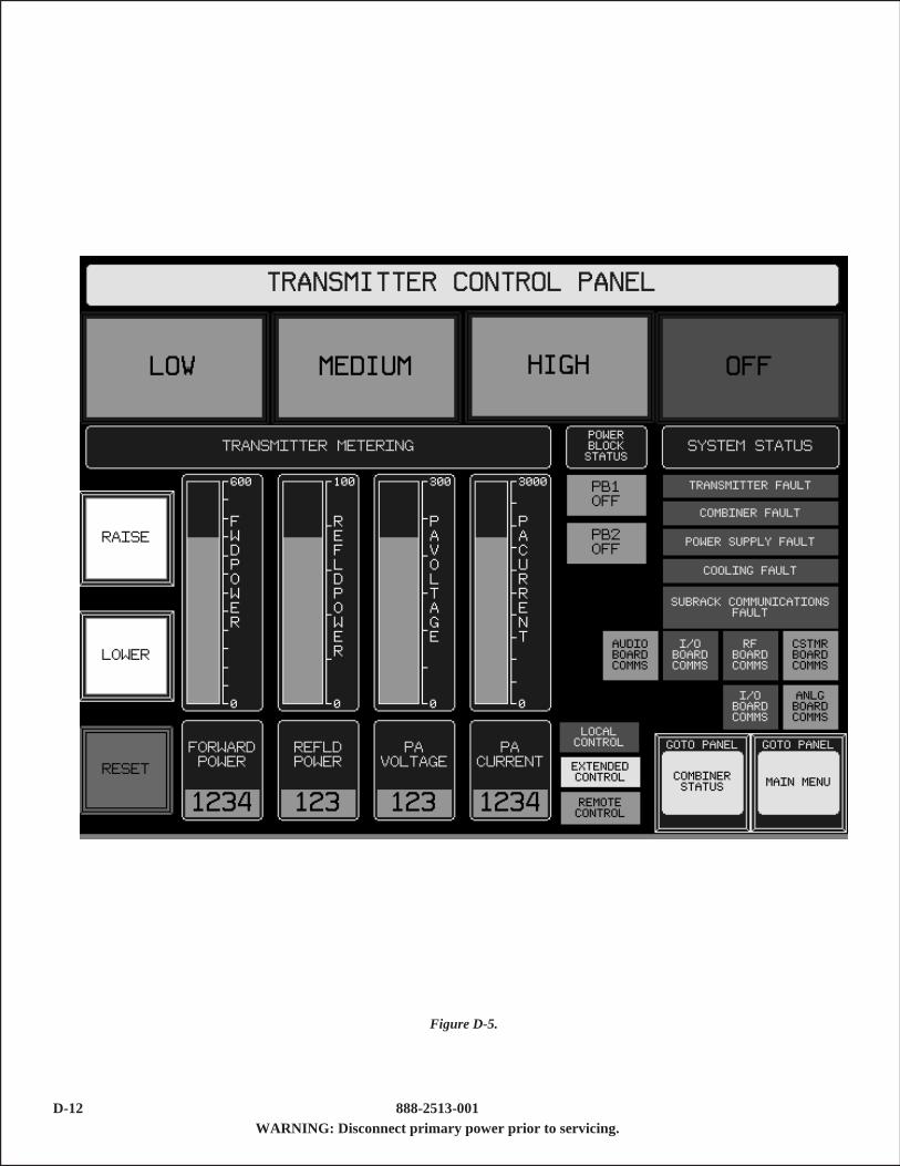
Figure D-5.
D-12 888-2513-001WARNING: Disconnect primary power prior to servicing.
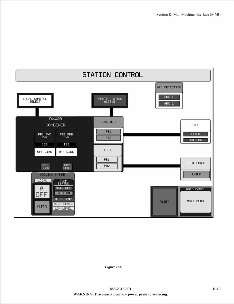
Figure D-6.
Section D, Man Machine Interface (MMI)
888-2513-001 D-13WARNING: Disconnect primary power prior to servicing.

Figure D-7.
D-14 888-2513-001WARNING: Disconnect primary power prior to servicing.

Figure D-8.
Section D, Man Machine Interface (MMI)
888-2513-001 D-15WARNING: Disconnect primary power prior to servicing.

Figure D-9.
D-16 888-2513-001WARNING: Disconnect primary power prior to servicing.

Figure D-10.
Section D, Man Machine Interface (MMI)
888-2513-001 D-17WARNING: Disconnect primary power prior to servicing.

Figure D-11.Screens Flow Diagram
D-18 888-2513-001WARNING: Disconnect primary power prior to servicing.

Section EKeylock Panel
E.1 Scope and PurposeThis section covers the Keylock Panel in the TCU rack. Topicsinclude function, location, block diagram description, detailedcircuit description, troubleshooting and removal/replacement.Go to the System Drawing for the actual keylock configurationas installed in a particular facility to get the exact keys that areneeded to access the various areas of the transmitter.The following information is for a “typical” installation and willnot match ALL installations.
E.1.1 FunctionThe function of the Keylock system is to prevent inadvertentaccess to the higher power/voltage areas of the systemwhile theystill have power applied. This is accomplished by having theseareas secured by locked panels. The keys to these panels arelocated in other areas of the transmitter. In order to acquire aparticular key, the power must be removed at the precedingstage(s).
E.1.2 LocationThe keylock panel is located in the TCU rack. One key for eachPower Block and one for the combiner are held captive in thepanel.
E.1.3 Power Block ServicingTo service a single Power Block, the appropriate key is switchedat the keylock panel in the TCU. The example will use PowerBlock 1. Once the key is rotated, the Power Block is shut offthrough its interlock string. This key is taken to the Power SupplyRectifier Cabinet (TCU). Once inserted and rotated, the DCearthing switch can be rotated to the Earthed position. The switchis now locked in the safe position. The PSR key can now beremoved and taken to Power Block #1 and used to unlock the RFearthing switch. Once the RF earthing switch is rotated to theEarthed position, it can be locked and the slave keys can now beremoved to access any of the 12 doors on Power Block 1 only.E.1.3.1 ExampleThe following example will show how the keylock system as-sures the safety of the technician:
• Assume that you wish access to the left front panel of thePower Amplifier Cabinet of Power Block 1.
• This cabinet requires a key labeled PB1 which is releasedby the RF Earthing Switch.
• In order to engage the RF Earthing Switch, a key labeledPSR1 must be obtained from the Rectifier 1 cabinet.
• To release this key, another key TCU1 must be obtainedfrom the Transmitter Control Unit.
• When this key TCU1 is removed from the TransmitterControl Unit, it turns off the Power Supply for Power Block1.
• Key TCU1 is then placed in the DC Earthing Switch ofRectifier 1 and the Earthing Switch is engaged. This will
prevent any DC voltage from going via the Rectifier to thePower Block.
• Key PSR1 is then released from the Rectifier cabinet andwill be inserted into theRFEarthing Switch of PowerBlock1.
• When the RF Earthing Switch is engaged, this will preventany RF from entering the Power Block from the Com-biner/Antenna System. It also releases the 4 PB1 keys.These 4 keys can then be used to unlock and allow accessto any of the 12 locked cabinets (such as the left front panelof the Power Amplifier Cabinet of Power Block number 1,the original objective).
Should access be required to the inside of any of the transformersor rectifiers, a key PS1 is required. To acquire this key, thePrimary Switch 1 must be turned to the off position.The 4 keys for a Power Block are identical, but keys from onePower Block will not work in a different Power Block, i.e. keysfrom Power Block 1 will not open panels in Power Block 2.
E.1.4 Power Supply Transformers and RectifierCabinet
To gain access to the Transformers or Rectifier Cabinets, the ACMains Primary Key must be inserted into the lock, and theprimary switch opened and locked in the Earthed position. Thiswill release the two slave keys (PS1). These keys can be removedand taken to the associated transformer or the Rectifier LowVoltageACDisconnect Switch to release theRectifier access keyREC1 that can open the rectifier access lock.
E.1.5 Combiner ServicingThere are four sections of the Power Block combiner that can beserviced. All cabinets are made safe through a series of stepsbefore they can be accessed. Refer to 843-5523-758 for Keylockinformation. The keylock sequence can be determined for allcombiner access modes for servicing.E.1.5.1 ExampleThe following will show how the Combiner is made safe for thetechnician (using Keylock Diagram 843-5523-758):
• Assume you wish to service one of the Lower rear Com-biner Cabinets.
• This requires theCOMB key to be released from the lowerCombiner cabinet Bay 3.
• To release these keys, four keys are required; RFM fromthe Combiner Earthing switch and three PS keys from thePrimary Disconnects.
• To obtain the PS1 key, the AC1 key must be inserted intothe PrimaryDisconnect switch and the handle thrown to thedisconnect position, releasing the PS1 keys.
• A PS1 key can now be released and taken to the CombinerCabinet Bay 3.
• APS2 key can be obtained in the samemanor as PS1 exceptthrough the other Primary Disconnect switch.
• To obtain the PS3 key, the Combiner LVDisconnect Switchmust be turned OFF.
888-2513-001 E-1WARNING: Disconnect primary power prior to servicing.

• The PS3 key can now be released and taken to theCombinerCabinet Bay 3.
• To obtain the RFM key, the Earthing Switch on the outputof the Combiner must be Earthed. To allow this, the ServiceCombiner Key, SCOM, from the TCU keylock panel mustbe inserted in the Earthing Switch.
• The RFM key can now be inserted into the CombinerCabinet Bay 3.
• With all four keys, the COMB keys can now be releasedand used to open the Lower Rear Combiner Doors.
These precautions ensure that there is no RF being produced,none can come into the combiner from the antenna, and no ACvoltages are in the cabinets.
E-2 888-2513-001WARNING: Disconnect primary power prior to servicing.

Appendix ALightning Protection Recommendation
a.1. IntroductionWhat do you dowith a 2million volt pulse
pushing 220,000 amps of current into yourtransmitting plant? Like the 500 pound go-rilla you let it dowhat ever it wants to. Thereis not much that can be done to protectagainst a major direct lightning strike. Thisis called a significant impulse lightningstroke. It usually lasts less than 100 micro-seconds and is most destructive to elec-tronic equipment because it contains hugeamounts of high frequency energy.Here are some examples of this damage:•Melted ball and horn gaps.•Ground straps burned loose.•H.V. rectifier stacks shorted.•Massive arc marks in the output circuitof AM transmitters.
•Ball lightning traveling into building onouter conductor of transmission line.
Figure A-1 is a map of the United Statesthat shows the number of lightning days youcan expect in any year. You fellas in Colo-rado, New Mexico, and Florida need light-ning rods on your hats.Figure A-2 shows the incidents to tall
structures. A triggered event is one thathappens because the tower was present.Without the tower the strike would not haveoccurred.
a.2. Environmental HazardsThere are devices and procedures that do
offer protection from lessor environmental
hazards than lightning. Some of theseanomalies are listed and defined:a. Over voltage/under voltage (brownout).Where the lines voltage differs from thenominal RMS for longer than one cycle.
•Remedy - Automatic voltage regulators,preferably individual regulators on eachphase. This can only be accomplishedwhen the power feed line is delta or4/wirewye connected. (See FigureA-3.)
b. Single phasing. This is where one leg ofthe three phase service is open.
•Remedy - Protection afforded by a lossof phase detector. Without protectionpower transformers and 3 phase motorsover heat.
c. Radio frequency interference (RFI). Thisis somethingwemust design into all of ourtransmitters, however, you may purchaseequipment that is susceptible, is not pro-tected, and develop problems.
•Remedy - RFI filters on the ac lines andcontrol lines are sometimes effective.Sometimes the entire device must beenclosed in an RF free space.
d. Electromagnetic pulse (EMP). This is ainterfering signal pulse that enters thesystem by magnetic coupling (trans-former). Generally caused by lightning.
•Lightning from cloud to cloud produceshorizontally polarized waves whilelightning from cloud to earth producevertically polarized waves. The wavescouple into the power lines and trans-
mission lines causing large induced volt-age that destroy high voltage rectifierstacks and output circuit faults. Highfrequency energy is coupled back intothe transmitter causing VSWR over-loads. (See Figures A-4 & A-5.)
•Remedy - Ball or horn gaps at the baseof the antenna prevent the voltage fromexceeding some high potential. Tran-sient suppresser devices on the inputpower lines remove excessive voltagespikes. Buried power and transmissionlines will reduce the amount of coupledenergy to a great extent. This does nottotally eliminate the problem becausethere are currents traveling in the earthwhen lightning strikes close to the sta-tion which prefer to travel on the metalconductors.
e. Surge. A rapid increase in voltage on thepower lines usually caused by lightning.The duration is less than 1/2 cycle andcan be very destructive.
•Remedy - Transient protectors are veryeffective in preventing damage to theequipment when properly designed andinstalled. (See Figure A-7.)
Significant Lightning Stroke CharacteristicsCharge Range 2 to 200 coulombsPeak Currents 2,000 to 400,000
AmperesRise Time to 90% 300 Nanoseconds to
10 MicrosecondsDuration to 50% 100 Microseconds
to 10 MillisecondsPotential Energy at99%
1010 Joules*
* Only a small portion is manifested in asurge, usually less than 10,000 Joules.
a.3. What Can Be Done?Installation of the transmitter building, an-
tenna tuning unit if applicable, and antennashould be done so that the risk of destructiondue to lightning is minimal and the effi-ciency of the over all system is maximized.To do this, separate ground systems shouldbe installed for the building and antenna.This forces all of the RF return currents toflow in the transmission line shield. Thecoax can be buried below the antennaground plane to still further reduce the RFcurrent coupled to it.Figure a-1. Isokeraunic Map of the United States
a-1WARNING: Disconnect primary power prior to servicing.

In medium and short wave installationsthe antenna ground plane is very importantas it is 1⁄2 of the radiating element. RFcurrent leaving the antenna must return viathe ground path (ground wave). For thisreason the “antenna coupling unit” must beclose to the base of the tower and securelyconnected to the ground plane.Figure A-6 shows the basic elements of a
properly designed antenna system.•Good ground plane.•Ball gap on tower.• Series inductor in tower feeder.•Antenna coupling unit connected to an-tenna ground.
•The π circuit is equivalent to the normalTee used by Harris.
•Underground coax.•Guy wire length broken by insulatorsand grounded at the bottom end.
The transmitter building must be givenextra protection to insure reliable equip-ment operation. A low impedance safetyground system must be installed using 3inch wide copper strap hard soldered at alljoints and connected to multiple groundrods located at the perimeter of the building.The ground rods should be wet to makegood connection to the earthwater table.Allequipment cabinets within the buildingmust be connected to the ground straps forsafety reasons.
a.4. AC Service ProtectionSee Figure A-7. All incoming ac lines
should have a choke connected in series tolimit the high frequency surges on the linesfollowed by a surge protector. The surgeprotector must be connected to the buildingground system by short direct connections.A surge protector is a solid state device
that is a high impedance until the voltageacross it reaches its rated clamping voltageat which time the impedance suddenly de-creases. The protector will then conducthundreds to thousands of amperes toground. All protectors are rated for maxi-mum voltage and maximum surge energy.If the surge energy exceeds rating of thedevice it will normally short and for thisreason must be fused so it will disconnectitself from the line being protected. Whenthis happens all protection is lost so somewarning system must be used to tell theoperators that a new protector should beinstalled.Speed is essential to protect equipment
from current surges with rates of rise ex-ceeding 10,000 amps per microsecond andpulses that last no longer than 100 micro-seconds. Very short, low inductance ground
straps are required to pass surges of thistype.The surge protectors must be selected for
the line to ground voltage and themaximumenergy to be diverted. Bigger is always bet-
ter in this case. There are several manufac-turers of surge protectors:
•Lightning Elimination Assoc., Inc.•Current Technology•Control Concept
Figure a-2. Lightning Incidents to Tall Structures
Figure a-3. Regulators in Delta and 4/Wire WYE Systems
a-2WARNING: Disconnect primary power prior to servicing.

•MCG Electronics, Inc.•EFI Corp.•General ElectricAll of these vendors provide parts and
systems to protect broadcast transmitters.All audio and control lines should be pro-
tected the same as described for ac lineswith components sized accordingly.All coaxial lines should have the shield
connected to the system ground at the point
of entrance and in addition have a ferritechoke around it located between the en-trance point and the equipment rack. Thiswill provide a high impedance for currentflowing in the shield but does not affect thesignal currents.
a.5. ConclusionThe 1% chance of a major lightning strike
probably can not be protected against butthe other 99%can be controlled and damage
prevented. Install surge protection on allincoming and outgoing lines at the wall ofthe building connected to a well designedground system. Properly install the antennaground system with spark gap adjusted cor-rectly and maintained. With this done youcan sleep peacefully at night if your bedisn’t under the feed line.
Figure a-4. EM Flux Field
Figure a-5. Sample Surge Voltage as a Function of
a-3WARNING: Disconnect primary power prior to servicing.

Figure a-6. Basic Elements of a Properly Designed
Figure a-7. Surge Protectors and Ferrite Choke
a-4WARNING: Disconnect primary power prior to servicing.