Embed Size (px)
Citation preview

EDS
N e w s l e t t e r
I E E E
ELECTRON DEVICES SOCIETY ELECTRON DEVICES SOCIETY ELECTRON DEVICES SOCIETY APRIL 2006 Vol. 13, No. 2 ISSN:1074 1879 Editor-in-Chief: Ninoslav D. Stojadinovic
Your Comments SolicitedYour comments are most welcome. Please write directly to the Editor-in-Chief of the Newsletter at [email protected]
The 26th Annual IEEE Symposium on VLSI Technology willbe held June 13-15, 2006, at the Hilton Hawaiian Village inHonolulu, Hawaii. The VLSI Technology Symposium is joint-ly sponsored by the IEEE Electron Devices Society (EDS) andthe Japan Society of Applied Physics (JSAP).
The VLSI Symposium is well recognized as one of thepremiere conferences on semiconductor technology, andresearch results presented at the conference represent abroad spectrum of VLSI technology topics, including:• New concepts and breakthroughs in VLSI devices and
processes. • New functional devices including quantum effect devices
with possible VLSI implementation.• Materials innovation for MOSFET and interconnect in VLSI.• Advanced lithography and fine patterning technologies
for high density VLSI.• Process/Device modeling of VLSI devices.• Packaging and reliability of VLSI devices.
Table of ContentsUpcoming Technical Meetings .......................1
• 2006 VLSI • 2006 ASMC
• 2006 IITC • 2006 UGIM
Outgoing Message from the 2004-5 EDS President ...................................3
Society News.........................................................9
• December 2005 AdCom Meeting Summary
• Message from the EDS Newsletter Editor-in-Chief
• EDS Educational Activities Committee Report
• EDS Nanotechnology Committee Report
• EDS Photovoltaic Devices Committee Report
• 2005 EDS J.J. Ebers Award Winner
• 2006 EDS J.J. Ebers Award Call for Nominations
• 2005 EDS Distinguished Service Award Winner
• 2006 Charles Stark Draper Prize
• 23 EDS Members Elected to the IEEE Grade of Fellow
• 2005 Class of EDS Fellows Honored at IEDM
• EDS Members Named Winners of 2006 IEEE Technical Field Awards
• EDS Regions 1-3 & 7 Chapters Meeting Summary
• 2005 EDS Chapter of the Year Award
• EDS Members Recently Elected to IEEE Senior Member Grade
• 2006 EDS Graduate Student Fellowship Final Call for Nominations
Regional and Chapter News .........................25
EDS Meetings Calendar ..................................30
EDS Archival Collection on DVD ...............32
(continued on page 8)
2006 IEEE Symposium
on VLSI Technology
Hilton Hawaiian Village, Honolulu, Hawaii
2006 IEEE Symposium
on VLSI Technology
13eds02.qxd 3/6/06 8:36 AM Page 1

2 IEEE Electron Devices Society Newsletter ❍ April 2006
President
Ilesanmi AdesidaUniversity of IllinoisE-mail: [email protected]
President-Elect
Cor L. ClaeysIMECE-mail: [email protected]
Treasurer
Juin J. LiouUniversity of Central FloridaE-Mail: [email protected]
Secretary
John K. LowellConsultantE-Mail: [email protected]
Jr. Past President
Hiroshi IwaiTokyo Institute of TechnologyE-mail: [email protected]
Sr. Past President
Steven J. HilleniusAgere SystemsE-mail: [email protected]
Vice-President of Awards
Alfred U. Mac RaeMac Rae TechnologiesE-Mail: [email protected]
Vice-President of
Educational Activities
Paul K. L. YuUniversity of California at San DiegoE-Mail: [email protected]
Vice-President of Meetings
Jon J. CandelariaMotorolaE-mail: [email protected]
Vice-President of Membership
Albert WangIllinois Institute of TechnologyE-mail: [email protected]
Vice-President of Publications
Renuka P. JindalUniversity of Louisiana at LafayetteE-Mail: [email protected]
Vice-President of Regions/
Chapters
Cor L. ClaeysIMECE-Mail: [email protected]
Vice-President of Technical Activities
Mark E. LawUniversity of FloridaE-Mail: [email protected]
IEEE Newsletters
Paul Doto, Paul DeSessoIEEE Operations CenterE-Mail: [email protected],[email protected]
Executive Director
William F. Van Der VortIEEE Operations CenterE-Mail: [email protected]
Business Coordinator
Joyce LombardiniIEEE Operations CenterEmail: [email protected]
IEEE Electron Devices Society Newsletter (ISSN 1074 1879) is published quarterly by the Electron Devices Society of the Institute of Electrical and ElectronicsEngineers, Inc. Headquarters: 3 Park Avenue, 17th Floor, New York, NY 10016-5997. Printed in the U.S.A. One dollar ($1.00) per member per year is included in theSociety fee for each member of the Electron Devices Society. Periodicals postage paid at New York, NY and at additional mailing offices. Postmaster: Send addresschanges to IEEE Electron Devices Society Newsletter, IEEE, 445 Hoes Lane, P.O. Box 1331, Piscataway, NJ 08855-1331.
Copyright © 2006 by IEEE: Information contained in this Newsletter may be copied without permission provided that copies are not used or distributed fordirect commercial advantage, and the title of the publication and its date appear on each photocopy.
EDS AdComElected Members-at-Large
Elected for a three-year term (maximum two terms) with ‘full’ voting privileges
2006 Term 2007 Term 2008 Term
S.S. Chung (1) J. N. Burghartz (1) G. Baccarani (1)T. Hiramoto (2) M. J. Chan (1) J. Deen (1)L. M. Lunardi (2) M. Estrada del Cueto (2) F. J. Garcia Sanchez (2)M. Lundstrom (1) S. Ikeda (1) J.B. Kuo (1)A. Wang (1) R. J. Nikolic (1) J.J. Liou (2)H.S.P. Wong (2) N. D. Stojadinovic (2) H. Shang (1)X. Zhou (1) J. J. Wesler (1) J. W. Swart (1)
S. Tyagi (1)
ELECTRON DEVICES
SOCIETY
ELECTRON DEVICES
SOCIETY
CONTRIBUTIONS WELCOMECONTRIBUTIONS WELCOME
Readers are encouraged to submit news items concerning the Societyand its members. Please send your ideas/articles directly to either the Edi-tor-in-Chief or appropriate Editor. The e-mail addresses of these individu-als are listed on this page. Whenever possible, e-mail is the preferredform of submission.
Newsletter DeadlinesIssue Due Date
January October 1stApril January 1stJuly April 1stOctober July 1st
REGIONS 1-6, 7 & 9
Eastern, Northeastern & South-
eastern USA (Regions 1, 2 & 3)
Ibrahim M. Abdel-MotalebNorthern Illinois UniversityE-Mail: [email protected]
Central USA & Canada
(Regions 4 & 7)
Jamal DeenMcMaster UniversityE-Mail: [email protected]
Southwestern & Western USA
(Regions 5 & 6)
Sunit TyagiIntelE-Mail: [email protected]
Latin America (Region 9)
Jacobus W. SwartState University of CampinasE-mail: [email protected]
REGION 8
Eastern Europe & The Former
Soviet Union
Alexander V. GridchinNovosibirsk State Technical UniversityE-mail: [email protected]
Scandinavia & Central Europe
Andrzej NapieralskiTechnical University of LodzE-Mail: [email protected]
UK, Middle East & Africa
Zhirun HuUniversity of ManchesterE-mail: [email protected]
Western Europe
Cora SalmUniversity of TwenteE-Mail: [email protected]
REGION 10
Australia, New Zealand &
South Asia
Xing ZhouNanyang Technological UniversityE-Mail: [email protected]
Northeast Asia
Kazuo TsutsuiTokyo Institute of TechnologyE-mail: [email protected]
East Asia
Hei WongCity University of Hong KongE-Mail: [email protected]
Editor-In-Chief
Ninoslav D. StojadinovicUniversity of NisE-Mail: [email protected]
NEWSLETTER
EDITORIAL STAFF
NEWSLETTER
EDITORIAL STAFF
13eds02.qxd 3/6/06 8:36 AM Page 2

April 2006 ❍ IEEE Electron Devices Society Newsletter 3
I would like totake the opportu-nity in completingmy term as Presi-dent of the Elec-tron DevicesSociety (EDS), toexpress my sin-cere appreciationto the members ofEDS, the EDS
Administrative Committee (AdCom)/Executive Committee (ExCom), andthe EDS Executive Office, who haveall worked hard together and support-ed me to reform our Society, which isnow facing a big change in the valueof the membership. In the past, theIEEE EDS journal subscriptions andIEEE EDS conference proceedingswere the main reason for individualsto become IEEE and EDS members.Now, regardless if they are membersor non-members, the employees andstudents of big companies and uni-versities who purchase the subscrip-tions and conference proceedingsfrom the IEEE, can access the journalsinstantaneously and free of chargethrough the web. Thus, the motiva-tion to join the IEEE EDS is gone forthe majority of the members. Now,what is the value of EDS for mem-bers, as well as non-members aroundthe world? EDS is a global societywhich organizes many top level inter-national conferences (such as theInternational Electron Devices Meet-ing - IEDM) and journals (such asElectron Device Letters - EDL andTransactions on Electron Devices - T-ED) for the companies and universi-ties to publish their technicalaccomplishments. In other words,electron devices engineers and theiraffiliated organizations can make theirachievement recognized world-wide,with its quality guaranteed by theIEEE EDS. Also, they can obtain thenewest technical information byattending these conferences and sub-scribing to the journals. Thus, EDS isa community consisting of the abovepeople and it is desirable that the
people, who enjoy the benefits of theEDS, support it by joining the Society.In the meantime, EDS has to establisha mechanism to make the Societyattractive enough to encourage themto join. This has been the consensusof the EDS as confirmed by ExComand AdCom for the past two yearsduring my term as President. Thus,we have been working to initiate anumber of new activities/programs tomake EDS attractive, to approve themat the AdCom, and to execute them.
Direct motivation for the confer-ence attendees to join the IEEE EDS isto change the conference registrationfee differential between members andnon-members to be larger than thecost of the membership fees of theIEEE plus EDS. We have been negoti-ating with the EDS sponsored confer-ences concerning the registration feedifferential between members andnon-members and we have receivedagreement from some of the confer-ences, such as the IEDM. We havealready started to send a solicitationletter to the first author of the papersaccepted to the EDS sponsored con-ferences and journals to join the IEEEEDS, if they are not already a mem-ber. It is a controversial topic now, butwe might have to think about charg-ing a moderate page fee for journalpaper publication to non-members inthe future, as done by some otherjournals. As I wrote in past issues ofthe EDS Newsletter, we issued a DVDarchive (EDS Archival Collection),which includes all the issues of T-ED,EDL, and the Technical Digests of theIEDM from their beginning. The col-lection is only offered to EDS mem-bers and at a very low price of $30USD ($9.95 USD for students). This isa great privilege and benefit for EDSmembers. Furthermore, we are in theprocess of planning a way to preservethe archives of the proceedings of asmany conferences for which EDS issponsoring, co-sponsoring and tech-nically co-sponsoring. Almost all ofthe proceedings since 1988 of EDSsponsored, co-sponsored and techni-
cally co-sponsored conferences, arepreserved on the IEEE Xplore system.However, there are only a few confer-ences with information on Xplore dat-ed prior to 1988. Different from thejournals, most of the archived confer-ence proceedings are not preservedin libraries and eventually will disap-pear in the years ahead. It is our dutyto make a plan and execute it, as soonas possible, before they disappear.New ideas and findings have beenpublished either at conferences or inthe letters type publications, and thensome of them are later published aslarger size articles in transactions andjournals. Thus, preserving the confer-ence archive is a very important ini-tiative. Regarding journal papers, thenumber of full paper versions of theconference-published papers in T-EDis decreasing significantly, althoughsome of them are published in non-IEEE journals. We are working withthe IEDM to have at least 25 bestpapers of the IEDM published peryear, in T-ED as invited papers. Wewill work with other conferences torecommend good papers to be pub-lished in T-ED.
EDS is a society that covers all thetechnical field of electron devices.We are working with EDS confer-ences, through EDS technical com-mittees, to watch newly emergingfields and to include the fields intoour Society by providing special ses-sions at conferences, creating topicalworkshops, or inviting specialists tothe conferences. Not only the emerg-ing fields, but also developing theexisting field is important. Displays,sensors and semiconductor manu-facturing, for examples are the fieldsin which EDS conference activity isnot so strong, and we need toenhance it. EDS has only a small por-tion of the electron devices manufac-turing engineers or industrial peopleas its members. In order to attractindustrial people, we are workingwith conferences such as the IEDMto provide industrial exhibitions atthe conferences.
Hiroshi Iwai
Outgoing Message from the
2004-5 EDS President
Outgoing Message from the
2004-5 EDS President
13eds02.qxd 3/6/06 8:36 AM Page 3
Besides conferences and journals,chapters are another fundamentallyimportant unit of EDS activities. Com-munication with local members canbe done through the chapters. Activi-ties of the EDS Regions/Chapters,Education, and Membership commit-tees can also be implemented throughthe chapters. Besides the benefit tothe members to attend top level lec-tures, having Distinguished Lecturers(DL) is one of the most importantopportunities for EDS to communicateto its members. We increased thenumber of the Distinguished Lecturers(DL) from 99 to 139, and lectures from122 to 142, over the past two years.Also, we organized 12 mini-colloquiaof DLs throughout the world over thepast two years. We will continue theeffort to further increase the numberof DLs. Asia (including China andIndia) and Latin America are thelargest growth areas for the electrondevices and engineers in the nearfuture. However, there are so manybig cities or areas where chapters donot exist. EDS has sent delegations to
meet the local people to solicit to formchapters in many areas of the world.As a result, the number of chaptershas increased from 109 to 120 in thepast 2 years, and the formation ofmany new chapters is now inprogress. However, it is still insuffi-cient to cover the areas, and this effortwill be strongly continued in futureyears. For most of the underdevel-oped countries, the IEEE membershipfee of about $120 USD is extremelyexpensive for the local people,although the EDS membership fee isonly $11 USD. Thus, EDS promotesthe Membership Fee Subsidy Pro-gram which allows 12 members in achapter to be subsidized each year.We approve the subsidy for foundingmembers of the new chapter, so that asufficient number (12) of the foundingmembers can be easily obtained.Also, we encourage non-members toobtain EDS affiliate memberships, asthe IEEE affiliation fee is about half theprice of the regular membership fee.
In order to promote educationalactivity, we will increase student relat-
ed awards and create a new EDS Edu-cation Award. EDS started the prac-tice of issuing certificates ofappreciation each year to the peoplewho contributed to the EDS, in addi-tion to those EDS AdCom memberswho step down each year from theirpositions.
These are the EDS initiatives forwhich I have been working with themembers and the EDS ExecutiveOffice as the President for the pasttwo years. Our philosophy is to pro-vide as much service as we can topromote the ED activities. These ini-tiatives will be continued by the newPresident, Ilesanmi Adesida; but it isyou, members of the EDS, who canimprove the EDS for yourself. We arelooking forward to your participationand feedback of our initiatives. Thankyou again for your great support forthe past two years.
Hiroshi Iwai2004 – 2005 EDS President
Tokyo Institute of TechnologyYokohama, Japan
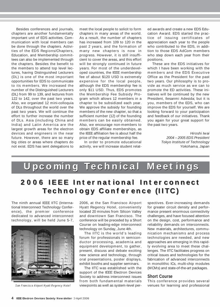
4 IEEE Electron Devices Society Newsletter ❍ April 2006
The ninth annual IEEE IITC (Interna-tional Interconnect Technology Confer-ence), the premier conferencededicated to advanced interconnecttechnology, will be held June 5-7,
2006, at the San Francisco AirportHyatt Regency Hotel, convenientlylocated 20 minutes from Silicon Valleyand downtown San Francisco. Theconference will be preceded by a ShortCourse on leading-edge interconnecttechnology on Sunday, June 4th.
The IITC is the world’s leadingforum for professionals in semicon-ductor processing, academia andequipment development, to gather,present, discuss and debate excitingnew science and technology, throughoral presentations, poster displays,exhibit booths and supplier seminars.
The IITC was established with thesupport of the IEEE Electron DevicesSociety to address interconnect issuesfrom both fundamental materialsviewpoints as well as system-level per-
spectives. Ever-increasing demandsfor greater circuit density and perfor-mance present enormous connectivitychallenges, and have focused attentionon the design, cost, performance andreliability demands on interconnects.New materials, architectures, commu-nication mechanisms and processtechnologies are needed, and newapproaches are emerging in this rapid-ly evolving area to meet these chal-lenges. The IITC facilitates progress oncritical issues and technologies for thefabrication of advanced interconnectsin monolithic ICs, multi-chip modules(MCMs) and state-of-the-art packages.
Short CourseThis conference provides severalvenues for learning and professional
Upcoming Technical MeetingsUpcoming Technical Meetings
San Francisco Airport Hyatt Regency Hotel
2006 IEEE International Interconnect
Technology Conference (IITC)
2006 IEEE International Interconnect
Technology Conference (IITC)
13eds02.qxd 3/6/06 8:36 AM Page 4

April 2006 ❍ IEEE Electron Devices Society Newsletter 5
interaction. The popular Short Courseonce again will address advancedinterconnect process, design and relia-bility issues. Participation is stronglyencouraged by those wishing to bene-fit from a combination of tutorials oninterconnect fundamentals, briefingson the latest interconnect technologyadvances, and direct interaction withexperts actively at work in the field.
Supplier Exhibits/SeminarsWithout doubt, the cost and perfor-mance of ULSI circuits strongly dependon the capability and productivity ofinterconnect materials and processingequipment. In recognition of this criti-cal role, supplier exhibits and seminarsare included as an integral part of theIITC technical program and will be heldon the first and second days of the con-ference. These exhibits and seminarsoffer additional learning and network-ing opportunities, and provide alterna-tive forums to address specifictechnological challenges.
PresentationsOral presentations and poster papersoffered during the conference span abroad range of interconnect technolo-gy topics, including:
1. Silicides/Salicides: Characteriza-tion, new materials and processes,electrical performance and processintegration issues for metal sili-cides/salicides.
2. Dielectrics: Dielectric materials(low k, high k, ARCs, etc.) anddeposition processes (vapordeposition, CVD, spin-on, etc.) for
interconnect applications3. CMP/Planarization: Dielectric/Metal
CMP processes, equipment andmetrology issues, and Alternateplanarization techniques.
4. Metallization: Metal depositionprocesses/equipment (PVD, CVD,ALD, electroplating) and materialscharacterization, with particularemphasis on advanced aluminumand copper metallization.
5. Process Integration: Multilevelinterconnect processes, clusteredprocesses, novel interconnectstructures, contact/via integration,metal barrier and materials inter-face issues, etc.
6. Process Control/Modeling: CMP,metal/dielectric deposition andetching processes, PVD, CVD, elec-troplating, etc.
7. Reliability: Metal electromigrationand stress voiding, dielectricintegrity and mechanical stability,thermal effects, passivation issues,interconnect reliability predic-tion/modeling.
8. Interconnect Systems: Intercon-nect performance modeling andhigh frequency characterization,interconnect system integrationand advanced packaging concepts(flip-chip, chip-on-chip, MCM, etc.),novel architectures.
9. System-on-a-Chip: Interconnect,design and processing of SOC,embedded memory processing,materials and integration, RF andhigh frequency passive compo-nents, noise and cross-talk issues
10. Dry Processing: Dry etching ofvias, trenches and damascene
structures, dry etching of metal,dry cleaning processes, plasmainduced damage, etc.
11. Alternative Interconnects: Advancedinterconnect concepts, optical andRF interconnect, superconductors,nanotechnology-based inter-connect, etc.
Given the rapid acceleration of inte-grated circuit technology, the last topicprovides an important forum for dis-cussion of the interconnect crisis andpotential paradigm shifts to novelinterconnect schemes.
Professionals involved in intercon-nect-related activities are stronglyencouraged to participate in this excit-ing conference. Detailed informationcan be obtained from the IITC website:http://www.ieee.org/conference/iitc.For additional information or inquiriesregarding supplier exhibits and semi-nars, please contact Wendy Walker,IITC Administrator at +1 301-527-0900Ext. 104, Fax: +1 301-527-0994, oremail: [email protected].
Christopher CaseGeneral Co-Chair – North America
BOC EdwardsMurray Hill, NJ, USA
Jeong-gun LeeGeneral Co-Chair - Asia
MagnaChip SemiconductorChungbuk-do, Korea
Didier LouisGeneral Co-Chair - Europe
CEA/LETIGrenoble, France
2006 IEEE/SEMI Advanced Semiconductor
Manufacturing Conference (ASMC)
“Advancing the Excellence of Semi-conductor Manufacturing”
ASMC 2006 continues a long traditionof unveiling breakthroughs in semicon-ductor manufacturing—from fab pro-ductivity and profitability to advancedprocess controls and device yield.
With more than 90 peer-reviewedtechnical papers, expert keynotes
and a relevant panel discussion,ASMC attracts engineers and man-agers from fabs around the worldwho want to advance their semicon-ductor manufacturing knowledgewith real solutions…direct from thefab. The IEEE/SEMI Advanced Semi-conductor Manufacturing Confer-ence (ASMC) is an internationalconference sponsored by the IEEE
Electron Devices Society (EDS), theIEEE Components, Packaging, andManufacturing Technology Society(CPMT), and SEMI.
The conference, which alternatesbetween the U.S. and Europe to bet-ter serve the interests of its interna-tional audience, returns to Boston,May 22–24, 2006, at the SheratonBoston Hotel.
2006 IEEE/SEMI Advanced Semiconductor
Manufacturing Conference (ASMC)
13eds02.qxd 3/6/06 8:36 AM Page 5

6 IEEE Electron Devices Society Newsletter ❍ April 2006
Peer-reviewed papers from nine-teen nations and more than 49 com-panies and institutions have beenselected for presentation in 14 ses-sions. This year’s event coversthese topics of interest to semicon-ductor manufacturing engineersand managers: • advanced metrology• advanced processes and materials• APC• cleaning and surface preparation• cost reduction• defect inspection• equipment reliability/productivity• factory automation/dynamics• defect inspection• equipment reliability/productivity• human resource development• lithography• yield enhancement/modeling• yield productivity.
The conference will recognize a“best paper award,” sponsored byToppan Photomasks, and a “beststudent paper award,” sponsoredby ISMI.
ASMC 2006 also features a dis-t inguished l ine-up of keynotespeakers to begin each day of theconference. On Monday, May 22,Deb Newberry, author and profes-sor, will present Nanotechnology:What is it and How Does it Apply to
Me? Monday closes with the popu-lar ASMC poster reception, spon-sored by KLA-Tencor. This sessionencourages interaction betweenposter authors and conferenceattendees.
On Tuesday, May 23, Dr. Chen-ming Hu, TSMC Distinguished Chairand Professor of Electrical Engi-neering & Computer Sciences, Uni-versity of California, Berkeley, willdiscuss CMOS issues. Tuesdayends with a thought-provoking pan-el discussion, moderated by TomCheney, editor of MICRO Magazine,and featuring a distinguished panelof industry leaders who will sharetheir views on globalization,growth, productivity and profitabili-ty. The topic is Maintaining the Pro-ductivity Curve: Is a Bigger WaferNeeded?
The third keynote, Dr. VenuMenon, Vice President and CMOS1Manager Silicon Technology Devel-opment, Texas Instruments, Inc., willdiscuss Challenges and Opportuni-ties for Volume Manufacturing at65nm and Beyond.
Back by popular demand are theluncheon round tables. Subject-mat-ter experts will lead round table dis-cussions on ASMC topics. Thesepresent excellent opportunities tomeet others in your interest area or
to learn more about new technicalsubjects.
As an added bonus, this year’sASMC includes a two-hour updateon the International TechnologyRoadmap on Semiconductors(ITRS). Industry experts will providean overview of various ITRS topicsincluding factory automation, front-end processes, lithography andyield enhancement. Presentationswill be followed by a panel discus-sion with Q&A.
Who should attend ASMC 2006?Semiconductor professionalsinvolved in production control,process control, process transfer,yield and cycle time improvement,cost reduction, preventive mainte-nance, line supervision, facilitiesfab operation, quality, training andeducation.
ASMC 2006 will take place at theSheraton Hotel, situated in thecharming and historic Back Bay sec-tion of Boston. The hotel is ideallylocated for business in one of Ameri-ca’s most historic and dynamiccities. Four miles from Boston’sLogan Airport, the Sheraton Hotel isclose to the Financial District, Down-town Crossing, the scenic CharlesRiver, many of Boston’s favoriteshops, restaurants, and museums,and a short walk to the PrudentialCenter and famous Newbury Street.
A block of sleeping rooms hasbeen reserved for conference par-ticipants at the Sheraton Hotel. Tomake a reservation, contact theSheraton Hotel by May 1st at +1617-236-2000 or toll-free +1 800-325-3535. To register online andfor directions, visit www.semi.org/asmc and click on the hotel infor-mation. Mention “ASMC” or“SEMI” to obtain the specialgroup rate.
For schedule information and toregister on-line, visit http://www.semi.org/asmc or contact Ms.Margaret Kindling, SEMI Washing-ton, D.C., ([email protected]).
Margaret KindlingASMC Program Manager
SEMI Washington, D.C.Washington, D.C., USAGreater Boston Convention & Visitors Bureau
13eds02.qxd 3/6/06 8:36 AM Page 6

April 2006 ❍ IEEE Electron Devices Society Newsletter 7
The 16th Biennial University/Govern-ment/Industry Microelectronics Sym-posium (UGIM’06) will be held in SanJose, California, June 25-28, 2006, onthe campus of San Jose State Universi-ty (SJSU). For the past 30 years thissymposium has had the unique mis-sion to bring together micro/nanofabri-cation researchers and educators fromthese three sectors, not only to presentnew technical results, but also the pro-grams, collaborations, and laboratoriesthat make them possible. Representa-tives of university micro/nanofabrica-tion laboratories traditionally attendUGIM to exchange information. Gov-ernment agencies such as NSF, Semat-ech, SRC, DARPA, AFRL and ONRregularly participate with updates onfunding opportunities. Industry part-nerships with universities (often withgovernment support) that open up newopportunities for both education andresearch are frequently presented here.The Electron Devices Society of theIEEE is a technical co-sponsor of theUGIM symposia.
This year’s host for the Symposiumis the College of Engineering of SanJose State University. The College hasbeen listed among U.S. News &World Report’s top undergraduateengineering programs in the U.S.A.,since hosting the ASEE Frontiers inEducation conference in the 1980’s.The following quotes from two SiliconValley leaders describe San JoseState’s role as a provider of engineer-ing talent to Silicon Valley.
“San Jose State’s College of Engi-neering and Silicon Valley grew uptogether…the College helped Industrywith job-ready graduates whosehands-on skills made Silicon Valleythe high technology leader.” DavidPackard, Hewlett Packard
“San Jose State’s Engineering Col-lege has had a very positive influenceon the development of Silicon Valley.Graduates of this Professional Schoolhave contributed to the developmentof Intel since Intel’s beginning in1968.” Robert Noyce, Intel
The UGIM’06 technical session willbegin on Monday, June 26th at 8:30AM in the auditorium of SJSU’s Col-lege of Engineering and end at noonon Wednesday, June 28th. This year’sSymposium will have two laboratoryopen houses. The first will be on Sun-day afternoon June 25 at 2:00 PM atthe Stanford Nanofabrication Facility(SNF) (http://snf.stanford.edu/). TheSecond will be held on Mondayevening at 5:00 PM at San Jose StateUniversity’s Microelectronics Process-ing Engineering Laboratory (MPEL).The open houses will consist of aninformal discussion session for man-agers and researchers from variousmicroelectronics laboratory facilitiesfollowed by tours of SNF’s andSJSU’s facilities. The discussion willfocus on issues such as funding,equipment acquisition, maintenance,staff, operational expenses, process-ing issues, industry interaction, collab-orations with other universities,intellectual property and compatibilityproblems.
Papers will cover the followingtechnical areas:• New initiatives in university micro-
electronics programs, courses, lab-oratories, technology transfer,industry interaction
• Government-University microelec-tronics research programs
• Microelectronic research projectsin the areas of materials, simula-tion, design, processes, testing,and reliability
• Process equipment development,manufacturing, statistical processcontrol and design of experiments
• MEMS programs, courses, applica-tions, processing, interactions, andresearch electronic packaging tech-nologies, processes and materials
• Standard silicon and compoundsemiconductors
• Bioengineering and Biotechnology• Nanotechnology and
nanofabrication• Metrology and sensors• University microelectronics research
facilities
Two distinguished speakers willgive invited talks at the conference:• Meyya Meyyappan (Director, Cen-
ter for Nanotechnology, NASAAmes Research Center)
• Yoshio Nishi (Director, StanfordNanofabrication Facility)
The city of San Jose is located inSilicon Valley and is the home tomany microelectronics companiessuch as Intel, AMD, Applied Mater-ial , Novel lus, Lam Research,National Semiconductor, LinearTechnology, Cadence Design Sys-tems, Synopsys, Mentor Graphics,Nvidia, Cisco, Atmel, Altera, andCypress Semiconductor. Located inNorthern California, San Jose is thelargest city in the San Francisco BayArea, third largest city in California,and the 10th largest city in the Unit-ed States. San Jose is within onehour driving distance of downtownSan Francisco and Santa Cruzbeaches and several hours drivingdistance to Napa Valley andYosemite National Park. It has onetheme park, and one water park.
For more information on the Sym-posium, please visit the symposiumwebsite at http://www.engr.sjsu.edu/ugim06, or contact David Parent,One Washington Square Hall, EEDepartment, SJSU, San Jose, CA,95192-0084 (E-mail: [email protected]).
David W. Parent2006 UGIM General ChairSan Jose State University
San Jose, CA, USA
2006 University/Government/Industry
Microelectronics Symposium (UGIM)
San Jose College of Engineering
2006 University/Government/Industry
Microelectronics Symposium (UGIM)
13eds02.qxd 3/6/06 8:36 AM Page 7

8 IEEE Electron Devices Society Newsletter ❍ April 2006
• Theories and fundamentals relat-ed to the above devices.
• New concepts and technologiesfor VLSI manufacturing.
In addition to the innovative techni-cal work presented at the confer-ence, a one-day short course on“Process Technologies for Continu-ous Scaling” will be offered on theday preceding the conference,Monday June 12th. This shortcourse offers an excellent opportu-nity for attendees to learn aboutthe latest advances in semiconduc-tor device and process technolo-gies from a series of tutorialspresented by industry experts.
Also preceding the conference isa satell ite workshop on SiliconNanoelectronics, which will be heldat the Hilton Hawaiian Village onJune 11-12. This workshop is spon-sored by the Electron Devices Soci-ety and covers al l aspects ofsilicon-based nanoelectronics. Forfurther information visit the web-site http://nano.nd.edu/si-nano.
One of the unique strengths of theVLSI Technology Symposium is itsassociation with the Symposium onVLSI Circuits, which is held each yearat the same location during the sameweek. The 2006 Symposium on VLSICircuits will also be held at the HiltonHawaiian Village on June 15-17, witha circuits-related short course offeredon June 14. In addition, a joint“Rump Session” on a topic of inter-est to both technologists and circuitdesigners will be held on the eveningof Wednesday, June 14. This jointsession will complement two addi-tional rump sessions held the sameevening on key issues of interest tothe VLSI technical community.
Among other unique featuresthat differentiate the Symposiumon VLSI Technology are its spiritof international collaboration andemphasis on creating an informalatmosphere where new ideas andtechnology direct ions can bedebated and discussed. The loca-tion of the VLSI Symposium typi-cal ly a l ternates between theUnited States and Japan, giving ita true international setting. Morethan 800 participants from aroundthe world attended the 2005 Tech-nology Symposium in scenicKyoto, Japan.
The 2006 venue in Honolulu,Hawaii also offers many scenic andcultural attractions. Travel to theother surrounding Hawaiianislands, each of which offers aunique setting and flavor, is alsorelatively easy. A luau banquethosted by the Symposium on Tues-day night offers attendees anopportunity to further experiencePolynesian food and culture. TheHilton Hawaiian Village hotel, locat-ed on world-famous Waikiki Beach,is a world-class facility that offers awide range of recreational opportu-nities. The Hotel is easily accessi-ble by taxi from nearby HonoluluInternational Airport.
For further information, pleasevisit our conference web site athttp://www.vlsisymposium.org, orcontact the following conferencesecretariats:
Secretariat for VLSI Symposia (USA) Widerkehr and Associates16220 S. Frederick Ave.Suite 312Gaithersburg, MD 20877 USA
Tel: +1 301 527 0900 ext. 103Fax: +1 301 527 0994E-mail: [email protected]
Secretariat for VLSI Symposia(Japan)c/o ICS Convention Design, Inc.Sumitomo Corp., Jinbocho Bldg.3-24, Kanda-Nishikicho, Chiyoda-kuTokyo 101-8449, Japan
Tel: +81 3 3219 3541Fax: +81 3 3292 1811E-mail: [email protected]
We cordial ly invi te you toattend the 2006 Symposium onVLSI Technology to learn aboutrecent state-of-the-art advance-ments in semiconductor technolo-gy and take advantage of themany opportunities for technicaland cultural interactions offeredby the Symposium.
Robert HavemannSymposium ChairmanNovellus Systems, Inc.
San Jose, CA, USA
Shin’ichiro KimuraSymposium Co-Chairman
Hitachi, Ltd.Tokyo, Japan
Jason WooProgram Chairman
UCLALos Angeles, CA, USA
Tohru MogamiProgram Co-Chairman
NEC Corp.Kanagawa, Japan
(continued from page 1)
2006 IEEE Symposium on VLSI Technology2006 IEEE Symposium on VLSI Technology
13eds02.qxd 3/6/06 8:36 AM Page 8

April 2006 ❍ IEEE Electron Devices Society Newsletter 9
Society NewsSociety News
The 2005 Annualmeeting of theIEEE ElectronDevices Societywas called toorder by Presi-dent, Hiroshi Iwai,on Sunday, 4December, atthe Washington,D.C. Hilton pre-
ceding the IEDM Conference.
Executive ReportsGiven Debt of Gratitude certificateswere elected members of AdCom, CorClaeys, James Dayton, Masao Fuku-ma, Mikael Ostling, Kwyro Lee, DavidPulfrey, Ken Galloway (Meetings V-P),Steve Hillenius (Fellows Chair), LucianKasprzak (Device Reliability Physics TCChair), and James Kuo (MembershipV-P) who are leaving in 2005. Alsoreceiving EDS Certificates were HisayoMomose (EDS Newsletter Editor-NEAsia), Doug Verret (T-ED Editor-in-Chief), Yuan Taur (EDL Editor-in-Chief),Gady Golan (EDS Newsletter Editor-Middle East/Africa), Adelmo Ortiz-Conde (EDS Newsletter Editor-LatinAmerica), and Werner Weber (addingESSDERC proceedings on Xplore).Awarded Years of Service certificatesfrom the EDS Executive Office wereLaura Riello, Marlene James, Jo AnnMarsh, Mariola Piatkiewicz andWilliam Van Der Vort.
Hiroshi’s address focused on theresults of the 2005 IEEE TAB meet-ings. Approved by TAB were the IEEEComputer Aided Design Council, andthe Systems Council. He discussed themodified assignments of societies andcouncils to Divisions to equalize thesize of each. For example, in Division I,CPMTS & LEOS have been reassignedand the Division now includes EDS,CASS, SSCS, ECAD Council and theNanotechnology Council. Hiroshireviewed the proposed TAB restruc-turing plans, and a new requirementfor conferences to submit budgets toIEEE 9 months in advance with a rec-
ommended minimum surplus of 20%.Moving to EDS, he shared his view onprogress EDS has made in the lasttwo years regarding service to mem-bers, membership, and global promo-tion of EDS activities. While significantadvancement has been made in theseareas, at issue is the value of EDSmembership since many of the origi-nal reasons, which centered on publi-cations, have changed. Over the nextcouple years, EDS must adapt new ini-tiatives to address membershipissues, preservation of archive for theproceedings of EDS sponsored, co-sponsored, technical co-sponsoredconferences/workshops, involvementfrom industry, improve publicationquality, and continue promotionworldwide.
Treasurer, Juin Liou, reportsthat EDS finances have done well in2005 but have not prospered as wellas in the past due to lower confer-ence income. He projected a $234Knet surplus for the year with a fore-cast $136K net in 2006. [Note: allfinancial information within thisreport is in US$.] Reserves rose to$4,103K. Increased operatingexpenses, and losses from publica-tions, T-DMR, and C&D Magazinealso took a toll on the final net.Membership fees will stay fixed thru2007, but EDL and T-ED costs will beraised by $2. In 2007, the page countfor EDL will increase while that forT-ED remains fixed.
V-P Reports On the membership side, EDS had
11,219 members in 2005 holdingfairly steady from 11,494 in 2004. Ofthese, 6,705 are regular members,3,700 are permanent members, 785are students, and 29 remain affiliatemembers. The demographics aregiven below.
John Lowell, reporting forMembership V-P, James Kuo,exemplified that the committee con-tinues its promotions through creditvoucher programs at IEDM, member-ship distributions at EDS confer-ences, promotion through theDistinguished Lecturer Program,using chapter subsidies to pay formemberships and subscriptions, andreinstated both TIP mailings, and theSenior Member Program. For 2006,AdCom approved the followingchanges in the Membership Fee Sub-sidy Program (MFSP): (1) EDS willnow accept IEEE/EDS renewals, (2)each member/student can only becovered under this program once,and (3) four of the 12 members/stu-dents each year must be newIEEE/EDS members/students.
Regions/Chapters V-P, CorClaeys, listed five new EDS chaptersformed this year: AP/ED/MTTMalaysia, C/COM/ED UniversidadCristobal Colon Student Branch, EDXian, ED Universidad del Sol StudentBranch, and ED Bahia. This brings thecurrent number of worldwide chaptersto 120. Nineteen other chapters are inthe discussion stage for 2006. Corannounced that ED/SSC Bangalore isEDS’ “Chapter-of-the-Year” in 2005.He also discussed a new appointment
John K. Lowell
December 2005 AdCom Meeting SummaryDecember 2005 AdCom Meeting Summary
EDS Membership Demographics for 2005 (statistics as of 10/31/05)
13eds02.qxd 3/6/06 8:36 AM Page 9

policy and other guidelines to revivethe Chapters Partners program. PaulYu, Education V-P, gave statistics onthe Distinguished Lecturer (DL) pro-gram. Both the number of lecturers(139) and the number of lectures given(142) have escalated from their 2004levels. As stated above, activity withthe EDS Videotape Lending Librarycontinues to decline. Plans are under-way to convert them to DVD, or donatethem to universities as the program isphased out. The EDS Graduate StudentFellowship Program had another suc-cessful year. This year’s winners wereSun-Jung Kim (Natl. University, Singa-pore), Tony Aik Sing Low (Natl. Univer-sity, Singapore), Elena Smotrova (Natl.Academy of Sciences, Ukraine), andChristopher Morris (Univ. of Washing-ton). Funding and recognition for theDL program was also outlined. In con-clusion, Paul outlined a new EduComGSF Award aimed at students who arestarting graduate work at the Masterslevel. The plan is to recognize worthystudents at the onset of graduatestudy, complimenting the original GSFwhich targets established doctoral stu-dents. Students would apply in theirsenior year of undergraduate work tocompete for one of five awards at $2Keach. Funding for the award receivedAdCom approval.
Renuka Jindal, Publications V-P,reported that paper circulation for EDL& T-ED fell below 5,000 for the firsttime in twenty years. While this is notalarming, as web-based circulation hasexpanded, it is viewed in parallel withthe declining EDS membership base.Discussion continues on the definitionof “nanotechnology” within EDS publi-cations. According to Renuka, if apaper refers to a “device” be it, elec-
tronic, photonic, or organic, then it fallswithin the realm of EDS interests. Inaddition, the confidentiality of paperreviews has been an issue this year. Insome instances, reviewer commentshave been used for situations not relat-ed to author feedback. While specificsare confidential, Renuka assured thatany use of this material outside of thereview process is assumed to be inap-propriate. On the financial side, thestate of C&D Magazine remains anissue. In the 2006 budget, three soci-eties are due to be charged $40K, andin 2007, both LEOS and CASS will bewithdrawing sponsorship; and as aresult EDS is projected to put in $65Kby itself. The fact that Division I haschanged, and is no longer representedby the societies under which the origi-nal magazine was formed is anotherfactor. Renuka has been workingbehind the scenes to come up with afinancial model that would allow themagazine to continue. Suggested for-mats are (1) an all-electronic journalsimilar to Transactions on Device andMaterials Reliability (T-DMR) or (2) aCommon Design Service model(where all issues will look the same). Adecision is due in early 2006 as towhether EDS will continue its sponsor-ship for 2007. Another publication withfinancial problems is T-DMR. For itsfirst four years of publication, T-DMRlost $257K, with EDS covering 50% ofthe loss. The journal is expected toexperience a surplus of about $44K in2005. In 2006, this is significantlyreduced, as the publication will receiveless revenue than expected from theAll Society Periodicals Packages(ASPP), due to the recent changes tothe distribution algorithm. The Adviso-ry Board is seriously considering
unbundling the journal in 2007 whichwill allow them to operate at a break-even level. Renuka reminded everyonethat the EDS Archival Collection DVD isonly available to EDS members, as ameans to increase the value of EDSmembership. In addition, there areplans for a pilot project to convert theIEDM short course videotapes to DVDto be sold on a member-preferentialbasis. A long-term plan to possiblyarchive the proceedings from twelvefully supported conferences (other thanIEDM), and thirty-five technically sup-ported conferences is also being dis-cussed. The Publications Committeehas been charged with deciding whichof these meetings is interested, andappropriate. This year’s Paul Rappa-port and the George E. Smith awardswinners (see the October EDS Newslet-ter for details) were given, and thereviewer luncheon was also discussed.Renuka unveiled a new pilot projecttentatively called “Ask EDS”. Theimpetus for this effort came from thefrequent questions from EDS membersaddressed to the EDL & T-ED editors.Through the new program, a talentpool of technical committee members,DLs, AdCom members, EDS members-at-large, and non-EDS experts wouldbe called upon to answer inquiries onvarious topics. The replies are intendedto be of a general nature with a liabilitydisclaimer. Hiroshi approved $5K tofund this project for one year.
Jon Candelaria, General Chairof the 2005 IEDM, expects 1,500attendees and 450 at the Short Cours-es. The financials project an expectedsurplus of $79K. Hot topics for the ple-nary and panel sessions are the impactfuture scaling of CMOS, display tech-nology, and non-volatile memories.Meetings V-P, Ken Galloway gotapproval for all EDS repeat meetingsin 2007, and gave statistics on thosefor 2005. This past year EDS supported25 financially sponsored meetings, 79that were technically co-sponsored,and none with cooperative support.Meeting closing continues to be prob-lematic and cost EDS $2.5K this year.Over the last five years, late closingsfees of $14.5K were charged to EDS.Continuing the topic of meetings,Technical Activities V-P, Mark Law haslooked at meeting relevancy. The issuehere is that many meetings deal with a
10 IEEE Electron Devices Society Newsletter ❍ April 2006
Presiding over the 2005 EDS Administrative Committee (AdCom) Meeting in Washington, D.C., are(left to right), William Van Der Vort, EDS Executive Director, Ilesanmi Adesida, EDS President-Elect
and Hiroshi Iwai, EDS President.
13eds02.qxd 3/6/06 8:36 AM Page 10

wide variety of topics making it diffi-cult to assign them to a specific techni-cal committee for guidance. Moreover,many meetings are “regional”,addressing themselves to attendeesfrom a defined locale, and cover abroad range and not just one specifictechnical area, falling outside the EDSmeeting mainstream. Interest in an“umbrella” meeting, wherein severalsmall meetings could meet simultane-ously sharing the cost, has been mini-mal. Mark will try to get a largermeeting to cooperate.
Chair ReportsAward’s V-P, Al Mac Rae, present-ed his list of EDS members recog-nized with major national, IEEE, andEDS awards in 2005. Summarized asfollows:
With the Fellows report, Chair-man, Steve Hillenius, stated thatfrom the 56 nominations EDSreceived, 11 EDS members were pro-moted to Fellow grade. There werealso another 12 EDS members electedFellow who were reviewed by othersocieties. EDL EIC Yuan Taur, reportsthat EDL published 269 papers thisyear, an increase of 8% over 2004. Heis planning to add a new AssociateEditor for molecular electronics. Divi-sion I Director, Lew Terman, present-ed on the state of the Division.Highlights of his report focused on thekey IEEE issues of membership,finances, and the TAB reorganization.Current IEEE membership is flat andtrends show a decrease of 2% yearlyin the U.S., and a 5% increase else-where. At this rate, in fourteen yearsthe ratio of U.S. to non-U.S. member-ship will be 50-50. Society member-ship is also declining at a 5% per yearrate. IEEE reserves now stand at$140M. The TAB restructuring is dri-ven by several issues one involvingthe financial situation of the IEEEComputer Society. In addition, TABhas become too big and unwieldy.The Board of Directors plans to reducethe infrastructure charges allotted toeach society. They are also looking toadd member benefits by adding spe-cial search engines to Xplore.
Technical Committee (TC) & General Business ReportsPhilip Wong’s Nanotechnology TC
has been busy with editor recommen-dations for EDL, Transactions on Nan-otechnology (T-Nano) & T-ED.Optoelectronics TC Chair, Leda Lunar-di reported on several tasks such asidentifying special issue topics andreviewing requests for sponsoredmeetings. Their list of hot topics for2006 includes photonic circuits, sili-con optoelectronics, free-space lasercommunications, and multimodefiber links. She also reviewed a pro-posed change in the agreement withOSA on the Journal of LightwaveTechnology (JLT). The new agree-ment gives all contributing societiesan equal share of the costs and thesurplus instead of being OSA domi-nant. The new agreement receivedAdCom approval. Enrico Sangiorgi,leader of the Technology ComputerAided Design (TCAD) TC, discussedthe preparation of a special, T-EDissue. In other reports, Paul Yureviewed the status of EDS participa-tion in the IEEE Expert Now (formerlyXELL) short course program. Thethrust is to offer 1-hour online learn-ing modules available 24x7 offeringthe latest information on emergingtechnology reported at IEEE confer-ence tutorials. Lu Kasprzak outlinedthe proposed financial changes for T-DMR. Since the formula for distribut-ing ASPP funds has changed, thepublication needs additional revenuein 2007. It is seriously considering tounbundle itself, meaning in 2007, itwill no longer be free. Subscriptionsfor soft copy, hard copy, CD and com-binations will be sold, and members
of sponsoring societies will be billedfor soft copy. Lu projects that 10% ofthe 13,000 combined memberships ofEDS and the Reliability Society wouldsubscribe, giving them revenue of$25K. AdCom approved the newfinancial structure. Pricing trade-offswith the co-sponsoring ReliabilitySociety will be discussed in 2006.
Publication ReportsReporting on T-ED, Editor-in-Chief,Doug Verret, showed that the pagecount for 2005 increased significant-ly due to the publication of two spe-cial issues. Speaking for T-DMR, theEIC, Tony Oates, stated that the pub-lication has been holding a steadypage count of about 730 pages forthe last two years. He is hoping foran increase in the near future. Its2004 downloads on Xplore havegrown to the 70th percentile. Trans-actions on Semiconductor Manufac-turing (T-SM), according to EditorDuane Boning, is publishing around640 pages each year, and will moveto IEEE Manuscript Central in 2006. Ithas just finished its five-year IEEEPeriodical Review.
Newly Elected EDS OfficesFor 2006, your elected EDS officersare President, Ilesanmi Adesida,President-Elect, Cor Claeys, Trea-surer Juin Liou, and Secretary,John Lowell. Re-elected to a secondAdCom term were Francisco GarciaSanchez (Universidad Simon Boli-var, Caracas, Venezuela) and JuinLiou (Univ. of Central Florida). New-
April 2006 ❍ IEEE Electron Devices Society Newsletter 11
EDS Recipients of National, IEEE, and EDS Awards for 2005
13eds02.qxd 3/6/06 8:36 AM Page 11

ly elected AdCom members includeJamal Deen (McMaster University,Ontario, Canada), James B. Kuo(National Taiwan University,Taipei), Giorgio Baccarani (Univer-sity of Bologna, Italy), Huil ingShang (IBM), Jacobus W. Swart(State University of Campinas,Brazil), and Sunit Tyagi (Intel).
The next meeting of EDS AdComwill be on Sunday, June 4, 2006, inNaples, Italy.
John K. LowellEDS Secretary
Lowell ConsultingDallas, TX, USA
12 IEEE Electron Devices Society Newsletter ❍ April 2006
Summary of EDS AdCom Actions – December 2005
I am writing thismessage after alapse of almost ayear. It is some-times astonish-ing to see howquickly the yearhas gone by. Asprofessionals, allof us are verybusy in ourwork. I hope that
this issue comes at a very prosper-ous time in your career.
I would like to take this oppor-tunity to thank three outgoingRegional Editors for outstandingservice to the Newsletter and Elec-tron Devices community. They areGady Golan (Region 8 - UK, MiddleEast & Afr ica) , Adelmo Ort iz -Conde (Region 9 – Latin America)and Hisayo Sasaki Momose(Region 10 – Northeast Asia). Theiroutstanding voluntary contribu-tions for the past six years, asregional newsletter editors, areexemplary to the rest of us.Replacing them on the NewsletterEditor ia l Staff are Zhirun Hu,Jacobus W. Swart and Kazuo Tsut-sui, respectively, whose biogra-phies follow. It is my pleasure towelcome them as new editors forthe EDS Newsletter.
Zhirun Hureceived his B. Engin telecommunica-tion engineeringfrom Nanjing Uni-versity of Postsand Telecommuni-cations, Nanjing,China, in 1982,
Master in Business Administration, andPh.D. in electrical and electronic engi-neering from the Queen’s University ofBelfast, United Kingdom, in 1988 and1991, respectively.
In 1991, he joined the Department ofElectrical and Electronic Engineering,University College of Swansea, as asenior research assistant in computa-tional semiconductor device simula-tion. In 1994, he rejoined theDepartment of Electrical and ElectronicEngineering, the Queen’s University ofBelfast, as a research fellow in siliconMMIC design, realization and charac-terization. In 1996, he joined GEC Mar-coni, as a microwave technologistworking on microwave/millimetre-wave device and circuit design andcharacterisation. He was a lecturer withthe Department of Electronic Engineer-ing, King’s College London from 1998to 2003. He joined the Department ofElectrical and Electronic Engineering,the University of Manchester, England,in January 2004.
His main research interests are inhigh frequency device and circuitmodelling, optimization, design, real-ization and characterisation. He haspublished 45 referred journal and con-ference papers
His most important IEEE activitiesinclude: (1) People to People Ambas-sador Programs Electron Devices Dele-gation to China led by Professor CaryY. Yang in 2001, and (2) IEEE UK & RIGOLD committee member.
Jacobus W. Swartreceived the B.Engineer and Dr.Engineer Degreesin 1975 and 1981respectively, fromthe PolytechnicSchool, University
of São Paulo, Brazil. Following, heworked at: K. U. Leuven, Belgium,1982-83; CTI, Campinas, 1984; LSI-Uni-versity of São Paulo, 1985-88; RTI,USA, 1991, and The School of Electricaland Computer Engineering, State Uni-versity of Campinas, since 1988;presently as Full Professor. Dr. Swarthas published 40 papers in Journalsand 150 full papers in Proceedings ofConferences. He has advised 32 Dr.and MSc. degree students. He is aSenior Member of IEEE, member of
Ninoslav D.Stojadinovic
MESSAGE FROM THE EDS NEWSLETTER
EDITOR-IN-CHIEF
MESSAGE FROM THE EDS NEWSLETTER
EDITOR-IN-CHIEF
13eds02.qxd 3/6/06 8:36 AM Page 12

ECS, SBMicro, SBMO and SBPC andhas been president of SBMicro twice,1988-90 and 1998-2000.
Kazuo Tsutsuireceived the B.S.,M.S, and Dr. ofE n g i n e e r i n gdegree from theDept. of AppliedElectronics, TokyoInstitute of Tech-nology, Japan, in
1981, 1983 and 1986, respectively. He
joined the Dept. of Physical Electronics(1986-1989) and Dept. of Applied Elec-tronics (1989-1992), Tokyo Institute ofTechnology as a Research Associate.Since 1992, he has been Associate Pro-fessor of Interdisciplinary GraduateSchool of Science and Engineering,Tokyo Institute of Technology. Current-ly, he is doing research on heteroepi-taxial growth of dissimilar materials onsemiconductors, integration of quan-tum effect devices, and process tech-nologies for nano-CMOS. He is amember of IEEE EDS, Japan Society of
Applied Physics, and IEICE of Japan.He has been Secretary of the IEEE EDSJapan Chapter since 2004.
Once again, I thank the outgoingeditors for their dedicated service tothe Newsletter and welcome the neweditors and wish them all success.Please contact your respective Region-al Editor directly with news items.
Ninoslav D. StojadinovicEDS Newsletter Editor-in-Chief
University of NisSerbia and Montenegro
The objectives ofthe EducationalActivities Com-mittee are to pro-vide the forumand opportunitiesfor members toexpand theirknowledge of ourtechnical fields.The Committee
also seeks to provide opportunitiesfor the Society to attract new mem-bers and to promote membershipand student activities. The Commit-tee’s membership strength in 2005was sixteen, and its members wereappointed by the President to reflectthe worldwide geographical spreadof the Society. The Vice President forEducation who chaired the commit-tee was Paul Yu of the University ofCalifornia, San Diego, USA, and theother members were K. S. Chari(Electronics Niketan, India); JamalDeen (McMaster University, Canada);Magali Estrada del Cueto (CINVES-TAV-IPN, Mexico); Yoshiaki Hagiwara(Sony Corporation, Japan); AgisIlliadis (University of Maryland, USA);Kevin T. Kornegay (Cornell Universi-ty, USA); Kei-May Lau (Hong KongUniversity of Science & Technology,Hong Kong); Juin Liou (University ofCentral Florida, USA); Rebecca J.Nikolic (Lawrence Livermore Nat.Lab., USA); Stephen A. Parke (BoiseState University, USA); Jayasimha S.Prasad (Maxim Corporation, USA);Marcel D. Profirescu (Technical Uni-
versity of Bucharest, Romania);Arlene A. Santos (Department ofDefense, USA); Sunit Tyagi (Intel,USA); and Philip Wong (StanfordUniversity, USA). The committeephysically met during the spring EDSAdministrative Committee (AdCom)meeting in Madrid, Spain, and fallAdCom meeting in Washington, D.C.Committee business was conductedmostly by electronic means betweenthe two meetings.
An important function of the Com-mittee is to maintain a vibrant Distin-guished Lecturer (DL) Program forthe Society. The DL Program existsfor the purpose of providing EDSchapters with a list of quality lectur-ers who can give talks at local chap-ter meetings and other occasions.The listing of Distinguished Lecturersalong with their topics and travelschedules is maintained on the EDShomepage. The listing is reviewedyearly and to remain on the roster, aDistinguished Lecturer must activelyperform lectures. The year 2005,ended with a roster of 139 lecturers.There were over 142 lectures con-ducted all over the world fromBelarus to Egypt to Seoul to the Unit-ed States by well over half of ourDistinguished Lecturers. To arrangefor a lecture, EDS chapters areencouraged to contact lecturersdirectly. A general guideline for thevisit, but not the absolute rule, is thatthe lecturer should be able to includethe meeting site with an alreadyplanned travel schedule at a small
incremental cost to the travel plan.Alternatively, a prior coincident trav-el plan would not be required if thelecturer is already located within anapproximate fifty mile radius of ameeting site. Although the conceptof the program is to have the lectur-ers minimize travel costs by combin-ing their visits with planned businesstrips, however EDS will assist in sub-sidizing lecturers’ travel as needed.
At the past EDS AdCom Meetinga few changes were approved inregards to the EDS DistinguishedLecturer Program. The nominationand selection process of DLs willnow be approved twice a year at theJune and December AdCom Meet-ings. Also, each DL must now give 2lecture talks within 2 years to remainas an active EDS DL. A certificate ofrecognition will now be presented tothe DLs who continue serving as aDL for 5 years.
In addition to the individual lec-tures, there were seven mini-collo-quia conducted last year. Themini-colloquia concept generallyinvolves sending about 2 or moreDistinguished Lecturers to travel to aregion/chapter and present the latestdevelopments in a particular field.The chapters/regions would beresponsible for handling all thearrangements of the event and onlyminimal financial support would berequired of EDS and could be cov-ered by the DL Program budget uponrequest. The seven were held inHong Kong, Japan, Korea, Mexico,
April 2006 ❍ IEEE Electron Devices Society Newsletter 13
Paul K.L. Yu
EDS Educational Activities Committee ReportEDS Educational Activities Committee Report
13eds02.qxd 3/6/06 8:36 AM Page 13

Singapore, Taiwan, and Boise, Idaho,respectively. Several mini-colloquiaare already being planned for 2006,and reports on the DL Program arepresented frequently in this newslet-ter. For more information, pleasecontact Laura Riello of the EDS Exec-utive Office ([email protected]). Feed-backs are actively solicited on theprogram from chapter chairs, lectur-ers, and members of the society.
The Graduate Student Fellow-ships Program (GSFP) for Ph.D. can-didates was established five yearsago under the auspices of the Com-mittee. For 2005, the Chair of theGSFP sub-committee was StephenParke. There were four awardsmade last year with the winnersbeing presented with their awardsat the IEDM in Washington D.C. Thewinners were Elena Smotrova of theNational Academy of Sciences ofUkraine, Ukraine; Christopher J.Morris of the University of Washing-ton, U.S.A; and Sung Jung Kim andTony A. S. Low of the National Uni-versity of Singapore, the Republic ofSingapore. Reports on these win-ners are published in this issue of
the Newsletter. Advertisement forthe next competition with the quali-fications required and the renumer-ations, are also published in thisNewsletter and other EDS publica-tions. We are appealing to all ourmembers to advertise the programamong potential candidates andnominators so that students areaware of this opportunity for fund-ing and recognition. With theseawards, we hope to assist the verybest students in our fields and alsoto make a positive impact on thefuture leaders of our Society.
The EDS AdCom recentlyapproved a new Masters level Grad-uate Student Fellowship. This newaward is for graduating collegeseniors to encourage them to go tograduate school and reward theirundergraduate research work. Weare waiting for formal IEEE approvalwhich may take place at the June2006 IEEE Meeting Series.
The Committee worked with theIEEE Educational Activities Board(EAB) on the new EducationalProducts Init iat ive that waslaunched in 2003, entitled, IEEE
Expert Now (formerly XELL). Thisis a continuing education programwhich seeks to deliver short cours-es over the web. This is an experi-mental program and EDS is one ofthe societies assisting in validatingthis program. EDS is currentlysponsoring four courses whichcontain lectures by Yuan Taur,Wayne Ellis, John Cressler, CurtRichter and Duncan Stewart .Arlene Santos has agreed to be theEDS Liaison to the EAB for theIEEE Expert Now program.
Lastly, the committee is continu-ously exploring ways and mecha-nisms of involving students andgold members in conferences andother activities of the Society. If youhave any suggestions or informationon these or any other activities thatyou may want us to engage in,please contact me at [email protected].
Paul K.L. YuEDS Vice-President of Educational Activities
University of California, San Diego
San Diego, CA, USA
The EDS Nan-o t e c h n o l o g yTechnical Com-mittee serves asthe technicalresource for theElectron DevicesSociety. We havecontinued renew-al of our commit-tee membership.
This year, the members are MarkReed (Yale University), Karen Maex(IMEC), Edwin Kan (Cornell Univer-sity), Joerg Appenzeller ( IBMResearch), Kaustav Banerjee (Uni-versity of California, Santa Bar-bara), Toshiro Hiramoto (Universityof Tokyo), Hiroshi Iwai (Tokyo Insti-tute of Technology), and H.-S.Philip Wong (Stanford University).The membership covers a broadrange of expertise from nanoscaleCMOS, nanowire, nanotubes, self-
assembly, molecular electronics,and other “nano” topics. Theycome from a variety of back-grounds (industry and academia)and geographic locations (U.S.,Japan, Europe).
Nanotechnology is a vibrant andfast growing field. We work on get-ting EDS more involved in the nan-otechnology field. In the past year,we have been active in severalactivities in the service of EDS.They include:
• reviewed several EDS meetingsponsorship proposals.
• Conducted a satisfaction surveyof the IEEE Transactions onNanotechnology Journal.
• Recommended a slate of candi-dates to T-ED Editor-in-Chief forpossible replacement of Editor inthe nanotechnology area
• Recommended a slate of candi-
dates to Transactions on Nanotech-nology for possible replacement of3 Editors in three major areas
• Recommended a slate of candi-dates to EDL Editor-in-Chief for pos-sible addition to the editorial boardin the molecular electronics area
In the coming year, we will continueto serve in the above areas. In addi-tion, we will conduct a survey of keynanotechnology conferences thatEDS should be actively involved in.We are always looking for newmembers and ideas for improve-ment. Please contact the committeechair, H.-S. Philip Wong, for sugges-tions and ideas.
H.-S. Philip WongEDS Nanotechnology
Committee ChairStanford UniversityStanford, CA, USA
14 IEEE Electron Devices Society Newsletter ❍ April 2006
Philip Wong
EDS NANOTECHNOLOGY COMMITTEE REPORTEDS NANOTECHNOLOGY COMMITTEE REPORT
13eds02.qxd 3/6/06 8:36 AM Page 14

Observations on Photovoltaics in China
If the nature of the15th PhotovoltaicScience and Engi-neering Confer-ence (PVSEC-15)is any indication,the health of thePV industry inChina is marchinginexorably towardworld-class status.
The meeting, held in Shanghai, Octo-ber 10-14, 2005, is one of the largestin the history of the Asian conferenceseries, and stands second only to theWorld Conference on PhotovoltaicEnergy Conversion held in Osaka inMay 2003. (The World Conferencesare joint meetings of the U.S. IEEEPhotovoltaic Specialists Conference,the European Photovoltaic SolarEnergy Conference and the AsianPhotovoltaic Science and EngineeringConference and are held on anapproximate 4-year rotation amongthe three conference organizations.)In addition to a technical programwith nearly 700 presentations, theConference also included an industri-al exhibits area that was host to over
220 companies, about 100 of whichcame from China itself.
The technical program reflectedChina’s rapid rise up the learningcurve toward technical par with thethree major PV communities, i.e.the United States, Europe andJapan. The majority of papers wereon silicon solar cells of one materialtype or another (single crystallineand polycrystalline Si, amorphousSi, microcrystalline Si, etc.), butalso included the full spectrum oftopics normally found at the otherconferences as well: fundamentalsand novel devices; thin film solarcells; compound semiconductorsolar cells; photovoltaic systems(both building integrated and gridconnected); module manufacturingand field testing; and space solarcells and systems as well as ses-sions on policy and economicsrelating to photovoltaic energy con-version implementation and use.According to the Conference Chair,Professor Dinghuan Shi, Presidentof the Chinese Solar Energy Soci-ety, the Chinese PV industry pro-duction capacity rose from about100MW in 2004 to 250MW in 2005.This rapid growth is spurred by offi-
cial Chinese Government policythat calls for 10% of total powergeneration in China to be fromrenewable sources by 2020, with atleast 1% guaranteed to be from PValone. The plan also calls for theentire western part of China to beserved by renewable energysources by the above date.
While it is clear that China’s internalmarket is huge and a first priority, theChinese PV industry also has taken aimat the world export market. Productsthat were on display in the exhibitsarea were of sufficient quality to com-pete effectively with suppliers from thetraditional “big three” producing areas(Japan, Europe and the U.S.). Beyondthat, a cell and module manufacturingequipment industry has emerged with-in China and although its quality andcapability could not be determined, it isreasonable to expect that lower costChinese equipment will enable lowermodule prices in world markets forChinese modules. Time will tell.
Dennis J. FloodEDS Photovoltaic Devices
Committee ChairNorth Coast Initiatives, Ltd.
Oberlin, OH, USA
The 2005 J.J.Ebers Award, theprestigious Elec-tron Devices Soci-ety award foroutstanding tech-nical contribu-tions to electrondevices, was pre-sented to Dr. BijanDavari of IBM,
Yorktown Heights, NY, at the Interna-tional Electron Devices Meeting inWashington, D.C., on December 5,2005. This award recognizes Dr.Davari “for contributions to deep-submicron CMOS technology andtheir impact on the IC industry.“
Bijan Davari was born in Tehran,
Iran. He received his B.S. degree inElectrical Engineering from SharifUniversity of Technology, Tehran in1977, and his M.S. and Ph.D. degreesin Electrical Engineering from Rens-selaer Polytechnic Institute, Troy, NY,in 1979 and 1984, respectively. Hethen joined IBM Research Division,Thomas J. Watson Research Center,Yorktown Heights, NY, where he firstworked on various aspects of scaledCMOS and BiCMOS technologies,under the tutelage of Bob Dennardand Tak Ning.
Dr. Davari then became the techni-cal leader of the research and devel-opment effort leading to the firstgeneration of high-performance, low-voltage deep-submicron CMOS
which offered sufficient system levelperformance to displace bipolar tech-nology in IBM mainframes andenable new faster UNIX servers. Pre-viously, all high-speed computersused bipolar or BiCMOS technology.This 2.5V, 0.25 µm channel-lengthCMOS technology solved key devicescaling and technical problems tointegrate shallow-trench-isolation,dual-doped poly gates, and abruptsilicided source-drain junctions. Thiswork, which Bijan presented at the1988 IEDM, set the standard for per-formance-optimized, low-powerCMOS and led to the adoption oflow-voltage standards in JEDEC andin the industry, which before thattime was firmly on a 3.3-5V path.
April 2006 ❍ IEEE Electron Devices Society Newsletter 15
Dennis J. Flood
EDS Photovoltaic Devices Committee Report
Bijan Davari
2005 EDS J.J. Ebers Award Winner
EDS Photovoltaic Devices Committee Report
2005 EDS J.J. Ebers Award Winner
13eds02.qxd 3/6/06 8:36 AM Page 15
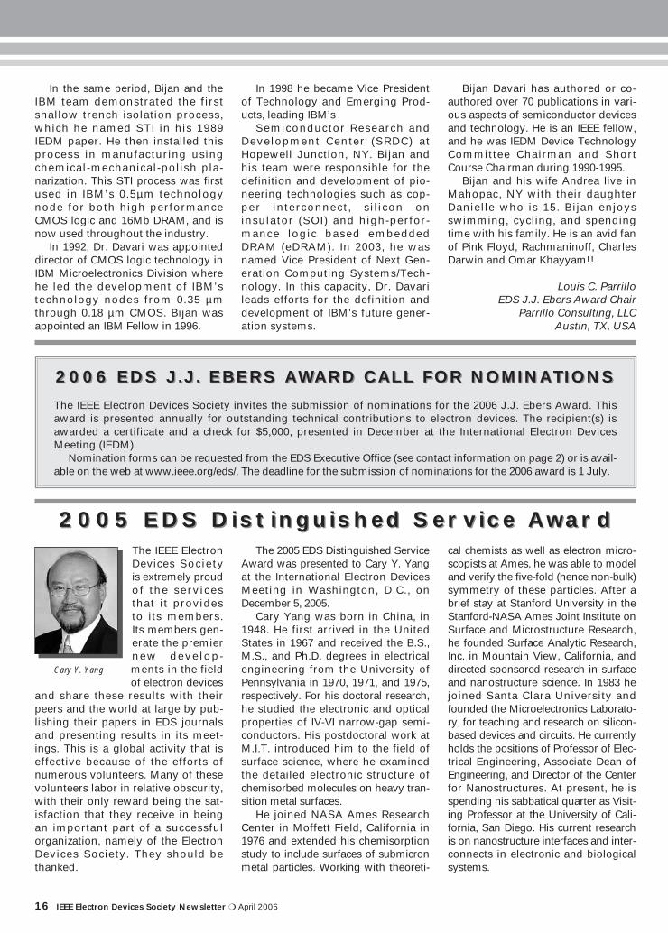
In the same period, Bijan and theIBM team demonstrated the firstshallow trench isolation process,which he named STI in his 1989IEDM paper. He then installed thisprocess in manufacturing usingchemical-mechanical-polish pla-narization. This STI process was firstused in IBM’s 0.5µm technologynode for both high-performanceCMOS logic and 16Mb DRAM, and isnow used throughout the industry.
In 1992, Dr. Davari was appointeddirector of CMOS logic technology inIBM Microelectronics Division wherehe led the development of IBM’stechnology nodes from 0.35 µmthrough 0.18 µm CMOS. Bijan wasappointed an IBM Fellow in 1996.
In 1998 he became Vice Presidentof Technology and Emerging Prod-ucts, leading IBM’s
Semiconductor Research andDevelopment Center (SRDC) atHopewell Junction, NY. Bijan andhis team were responsible for thedefinition and development of pio-neering technologies such as cop-per interconnect, sil icon oninsulator (SOI) and high-perfor-mance logic based embeddedDRAM (eDRAM). In 2003, he wasnamed Vice President of Next Gen-eration Computing Systems/Tech-nology. In this capacity, Dr. Davarileads efforts for the definition anddevelopment of IBM’s future gener-ation systems.
Bijan Davari has authored or co-authored over 70 publications in vari-ous aspects of semiconductor devicesand technology. He is an IEEE fellow,and he was IEDM Device TechnologyCommittee Chairman and ShortCourse Chairman during 1990-1995.
Bijan and his wife Andrea live inMahopac, NY with their daughterDanielle who is 15. Bijan enjoysswimming, cycling, and spendingtime with his family. He is an avid fanof Pink Floyd, Rachmaninoff, CharlesDarwin and Omar Khayyam!!
Louis C. ParrilloEDS J.J. Ebers Award Chair
Parrillo Consulting, LLCAustin, TX, USA
The IEEE ElectronDevices Societyis extremely proudof the servicesthat it providesto its members.Its members gen-erate the premiernew develop-ments in the fieldof electron devices
and share these results with theirpeers and the world at large by pub-lishing their papers in EDS journalsand presenting results in its meet-ings. This is a global activity that iseffective because of the efforts ofnumerous volunteers. Many of thesevolunteers labor in relative obscurity,with their only reward being the sat-isfaction that they receive in beingan important part of a successfulorganization, namely of the ElectronDevices Society. They should bethanked.
The 2005 EDS Distinguished ServiceAward was presented to Cary Y. Yangat the International Electron DevicesMeeting in Washington, D.C., onDecember 5, 2005.
Cary Yang was born in China, in1948. He first arrived in the UnitedStates in 1967 and received the B.S.,M.S., and Ph.D. degrees in electricalengineering from the University ofPennsylvania in 1970, 1971, and 1975,respectively. For his doctoral research,he studied the electronic and opticalproperties of IV-VI narrow-gap semi-conductors. His postdoctoral work atM.I.T. introduced him to the field ofsurface science, where he examinedthe detailed electronic structure ofchemisorbed molecules on heavy tran-sition metal surfaces.
He joined NASA Ames ResearchCenter in Moffett Field, California in1976 and extended his chemisorptionstudy to include surfaces of submicronmetal particles. Working with theoreti-
cal chemists as well as electron micro-scopists at Ames, he was able to modeland verify the five-fold (hence non-bulk)symmetry of these particles. After abrief stay at Stanford University in theStanford-NASA Ames Joint Institute onSurface and Microstructure Research,he founded Surface Analytic Research,Inc. in Mountain View, California, anddirected sponsored research in surfaceand nanostructure science. In 1983 hejoined Santa Clara University andfounded the Microelectronics Laborato-ry, for teaching and research on silicon-based devices and circuits. He currentlyholds the positions of Professor of Elec-trical Engineering, Associate Dean ofEngineering, and Director of the Centerfor Nanostructures. At present, he isspending his sabbatical quarter as Visit-ing Professor at the University of Cali-fornia, San Diego. His current researchis on nanostructure interfaces and inter-connects in electronic and biologicalsystems.
16 IEEE Electron Devices Society Newsletter ❍ April 2006
Cary Y. Yang
2005 EDS Distinguished Service Award2005 EDS Distinguished Service Award
The IEEE Electron Devices Society invites the submission of nominations for the 2006 J.J. Ebers Award. Thisaward is presented annually for outstanding technical contributions to electron devices. The recipient(s) isawarded a certificate and a check for $5,000, presented in December at the International Electron DevicesMeeting (IEDM).
Nomination forms can be requested from the EDS Executive Office (see contact information on page 2) or is avail-able on the web at www.ieee.org/eds/. The deadline for the submission of nominations for the 2006 award is 1 July.
2006 EDS J.J. EBERS AWARD CALL FOR NOMINATIONS2006 EDS J.J. EBERS AWARD CALL FOR NOMINATIONS
13eds02.qxd 3/6/06 8:36 AM Page 16

Over the past two decades, he hasinitiated innovative programs to edu-cate and train technical professionalsin various stages of their careers. Inthe eighties, he developed and orga-nized short courses on timely topicsin silicon technology to Silicon Valleyprofessionals. In the mid-nineties, heoffered short courses on semiconduc-tor technology for SEMI as part of aretraining program for professionalsin other fields. Since the mid-eighties,he has provided opportunities for hisstudents to spend extended periodsin companies in Japan, where theycollaborated with their hosts on theirthesis research. More recently, hefounded the Center for Nanostruc-tures at Santa Clara, which offersinterdisciplinary research and edu-cation opportunities in the field ofnanoscience and nanotechnologyfor university students and faculty,
high school students and teachers,as well as Silicon Valley technicalprofessionals.
He has been a consultant to indus-try and government, and a visitingprofessor at Tokyo Institute of Tech-nology, University of Tsukuba,National University of Singapore,University of Pennsylvania, Universi-ty of California, San Diego, and Uni-versity of California, Berkeley. He waselected Fellow of IEEE in 1999. Heserved as an editor of the IEEE Trans-actions on Electron Devices, in thearea of MOS devices. In 2001, onbehalf of People to People Ambas-sadors Program, he led an ElectronDevices Delegation to visit universi-ties, government institutes, and com-panies in the People’s Republic ofChina. In 2004, he was named therecipient of the IEEE EducationalActivities Board Meritorious Achieve-
ment Award in Continuing Education“for extensive and innovative contri-butions to the continuing educationof working professionals in the fieldof micro/ nanoelectronics”.
Cary resides in Cupertino, Califor-nia with his partner, Marie, a classi-cal singer. His elder daughter, Elaine,an aspiring impressionist painter,works as a technical recruiter in a Sil-icon Valley semiconductor company.His younger daughter, Jocelyn, stud-ies computer science and biology atthe University of California, SanDiego. He spends his spare timeplaying tennis and hiking on varioustrails in Silicon Valley.
H. Craig C. Casey, Jr.EDS Distinguished
Service Award ChairDuke University
Durham, NC, USA
April 2006 ❍ IEEE Electron Devices Society Newsletter 17
The National Academy of Engineeringawarded the 2006 Charles Stark Drap-er Prize to Willard S. Boyle and GeorgeE. Smith in recognition of their patent,“Information Storage Devices”,which describes the basic technolo-gy concept of Charge-CoupledDevices. The citation reads, “For theinvention of the Charge-CoupledDevice (CCD), a light sensitive com-ponent that is at the heart of digitalcameras and other widely usedimaging technologies.” The prize of$500,000 is shared by the recipientsand is an annual award that honorsengineers whose accomplishmentshave significantly benefited society.
CCDs are the key component indigital cameras and camcorders,fax machines and scanners, recon-naissance and weather forecastingsatellites, space and terrestrial tele-scopes, and miniature medicalimaging devices. The digital output ofa CCD is readily processed to enhanceimages, capable of being transmittedover great distances and stored forfuture use. Our easy ability to improveand manipulate images is a delightfulbenefit of using digital cameras. Pho-tographic film cameras are rapidlybeing replaced by these CCD based
cameras in the consumer productmarket-place. It goes without sayingthat a CCD is in billions of dollars ofproduct that are shipped every year.
George Smith is well known by IEEEElectron Devices Society members asthe first and long time editor of therapid publication; peer reviewed andwidely read “Electron Device Letters”.Indeed, the EDS George E. SmithAward is given annually for the bestpaper in this journal.
As the story of the CCD goes, Jack
Morton, then Vice President of the Elec-tronic Material and Components Areaof Bell Telephone Laboratories askedBill Boyle, one of his Executive Direc-
tors, if there were an electrical ana-log to the magnetic bubble device,where small magnetic domains, orbubbles, were moved under theinfluence of a magnetic field.Research on magnetic bubble mate-rials and their application to staticmemory and logic devices wasactively pursued at Bell Labs at thattime. Bill Boyle went to GeorgeSmith, then Head of the ImagingDevice Department, and their brain-storming session resulted in thebasic concept of the CCD. The appar-ent simplicity of the CCD was appeal-ing. The Bell Labs organizationsupported and encouraged suchinnovation - and it thrived in thisenvironment. Every new idea is the
product of its time and CCDs were noexception. These were exciting times atBell Labs and the semiconductor insti-tutions of the world.
Alfred U. Mac RaeEDS Vice-President of Awards
Mac Rae TechnologiesBerkeley Heights, NJ, USA
2006 Charles Stark Draper Prize
William Boyle (left) and George Smith (right)demonstrating a TV camera that uses a CCD.
2006 Charles Stark Draper PrizeP
HO
TO
CO
UR
TE
SY
OF
LU
CE
NT
TE
CH
NO
LOG
IES
, BE
LL L
AB
S
13eds02.qxd 3/6/06 8:36 AM Page 17

18 IEEE Electron Devices Society Newsletter ❍ April 2006
Muhammad Alam, Purdue Uni-versity, West Lafayette, IN, USA- for contributions to complemen-tary metal oxide semiconductors(CMOS) circuit reliability and com-putational models for electronicsand optoelectronics
Jesus del Alamo, MassachusettsInstitute of Technology, Cambridge, MA, USA- for contributions to microelectronic devices
Seshu Desu, University of Massachusetts-Amherst, Amherst, MA, USA- for contributions to developmentof ferroelectric thin film devices
Andreas Andreou, Johns Hop-kins University, Baltimore, MD, USA- for contributions to energy efficient sensory microsystems
Gary Bernstein, University ofNotre Dame, Notre Dame, IN, USA- for contributions to techniquesfor fabricating nanoscale devices and circuits
Steve Chung, National ChiaoTung University, Hsinchu, Taiwan- for contributions to reliability inultra-thin-oxide complementarymetal oxide semiconductor (CMOS) devices
Simon Deleonibus, CEA LETI,Grenoble Cedex 9, France- for contributions to nanoscaledcomplementary metal oxide semiconductor (CMOS) devicestechnology
Hector De Los Santos,NanoMEMS Research, LLC, Irvine, CA, USA- for contributions to radio fre-quency (RF) and microwave microelectro-mechanical systems(MEMS) devices and applications
Martin Giles, Intel Corporation,Hillsboro, OR, USA- for contributions to technologycomputer aided design (TCAD)modeling of processes anddevices
Hideki Hayashi, Sumitomo Electric Industries, Tokyo, Japan- for contributions to and leader-ship in compound semiconductordevice technologies
Larry Hornbeck, Texas Instru-ments DLP Products, Van Alstyne,TX, USA- for invention, development, andapplications of the DigitalMicromirror Device
Qin (Alex) Huang, North Caroli-na State University, Raleigh, NC, USA- for contributions to emitter turn-off thyristor technology and itsapplications
Muhammad Khan, University ofSouth Carolina, Columbia, SC, USA- for contributions to the develop-ment of III-nitride electronic sen-sor systems
Mong-Song Liang, TSMC (Tai-wan Semiconductor Manufactur-ing Company, Ltd), Hsin Chu,Taiwan, ROC- for contributions to semiconduc-tor manufacturing technologies
Gary May, Georgia Institute ofTechnology, Atlanta, GA, USA- for contributions to semiconduc-tor manufacturing and engineeringeducation
David Seiler, National Instituteof Standards and Technology,Gaithersburg, MD, USA- for leadership in the develop-ment of critical metrology andmeasurement science at the microand nano levels
Goran Stemme, Royal Instituteof Technology, Stockholm, Sweden- for contributions to micro elec-tro-mechanical systems (MEMS)
Yu-Chong Tai, California Insti-tute of Technology, Pasadena, CA, USA- for contributions to integratednano/micro electro-mechanicalsystems (MEMS) and nano/micro-fluidics for Lab-on-a-Chip applica-tions
Katsuyoshi Washio, CentralResearch Laboratory, Hitachi, Ltd.,Kokubunji, Tokyo, Japan- for contributions to high-speedsilicon and silicon germaniumbipolar/Bi complementary metal oxide semiconductors(CMOS) device and circuit technologies
Werner Weber, Infineon Tech-nologies, Munich, Germany- for contributions to metal oxidesemiconductors (MOS) devicephysics
Burnell West, Credence SystemsCorporation, San Jose, CA, USA- for contributions to high-perfor-mance automatic test equipment
Gerald Witt, Air Force Office Scientific Research, Arlington, VA, USA- for the promotion of research in compound semiconductordevices
Usha Varshney, National Sci-ence Foundation, Arlington, VA, USA- for technical leadership in sensortechnologies and systems
Steven J. Hillenius2005 EDS Fellows Chair
Agere SystemsAllentown, PA, USA
23 EDS Members Elected to the IEEE Grade of Fellow - Effective 1 January 2006
23 EDS Members Elected to the IEEE Grade of Fellow - Effective 1 January 2006
13eds02.qxd 3/6/06 8:36 AM Page 18

April 2006 ❍ IEEE Electron Devices Society Newsletter 19
On December 5, 2005, at the Ple-nary session of the IEEE EDSInternational Electron DevicesMeeting (IEDM) in Washington,D.C., the 2005 EDS President,Hiroshi Iwai, presented a num-ber of 2005 IEEE/EDS Fellowswith certificates to congratulatethem on being elected IEEE Fel-lows. Fourteen of the 40 EDSmembers elected to the IEEEgrade of Fellow for 2005 attendedthe presentation.
2005 CLASS OF
EDS FELLOWS
HONORED AT
IEDM
EDS President, Hiroshi Iwai (bottom row, 2nd from right), along with 14 EDS members whowere elected IEEE Fellow for 2005 at the 2005 IEDM.
EDS MEMBERS NAMED WINNERS OF THE
2006 IEEE TECHNICAL FIELD AWARDS
Four EDS Members were amongthe winners of the 2006 IEEE Tech-nical Field Awards. They are:
Louis C. Parrilloof Parrillo Con-sult ing, LLC. ,Aust in, Texas,won the 2006IEEE FrederikPhil ips Award.His citationstates, “For lead-
ership in advancing CMOS andBipolar technology through techni-cal and managerial contributions”.
Louis C. Parrillo received hisBSEE from the University of Con-necticut and his MSEE, MA andPh.D. degrees in Electrical Engi-neering from Princeton University.
He joined Bell Laboratories inMurray Hill, New Jersey (1972),where he and his colleagues devel-oped AT&T’s first all-implanted,
high-speed bipolar technology,including solutions to yield-limit-ing mechanisms that becamewidely adopted. With Dr. RichardPayne and their colleagues, hedeveloped the original and severalgenerations of “Twin-Tub CMOS”technology which became anindustry standard for high-perfor-mance CMOS.
In December, 1984 he joinedMotorola’s Advanced ProductsResearch and Development Labo-ratory (APRDL) in Austin. In 1988he was appointed Vice Presidentand Director of APRDL, building itto be an effective, internationally-recognized team. With TRW, theteam produced the world’s largestand most advanced “Superchips”(~1,500mm2 die s ize , 0 .5um,tr iple- level-metal technology),successfully completing the USgovernment’s CMOS VHSIC pro-gram (1989).
With manufacturing he drovethe creat ion of Motorola’sResearch, Development and Manu-facturing complex known today asthe Dan Noble Center. This effortenabled Motorola to independent-ly manufacture leading-edge Pow-er-PC products and la id thegroundwork for several externaltechnology alliances. As a Corpo-rate Officer (1994) and DivisionGeneral Manager (1997) he drovethe development of ul tra- fastSRAM products that were thefastest, most compact and the firstin the industry using copper-inter-connect technology. As Semicon-ductor’s Chief Technology Officerand Director of the DigitalDNA‰Labs (2001), he and his colleaguesdrove the alliance among Motoro-la, ST Microelectronics, PhilipsSemiconductor and TSMC for 300mm research and development inCrolles, France.
2005 CLASS OF
EDS FELLOWS
HONORED AT
IEDM
EDS MEMBERS NAMED WINNERS OF THE
2006 IEEE TECHNICAL FIELD AWARDS
13eds02.qxd 3/6/06 8:36 AM Page 19

After retiring from Motorola, heestablished Parrillo Consulting,LLC (2004) to provide technical,managerial and business value todiverse clients.
He has 27 patents and over 40publications. He is an IEEE Fellow(1989), a recipient of the ElectronDevices Society (EDS) J.J. EbersAward (with Dr. Richard Payne,1992), a past President of EDS(1996, 1997), a member of TheUnited States National Academy ofEngineering (1996), and a recipientof the EDS Distinguished ServiceAward (2004).
Dr. Parrillo and his wife Kath-leen reside in Austin. Their chil-dren, Jeffrey and Lisa are students.His outside interests include trackdriving in High-Speed Drivers Edu-cation events, photography andhiking with his family in Colorado.
C h a n g - G y uHwang of Sam-sung ElectronicsCo., Ltd, Gyeong-gi-Do, Korea, wonthe 2006 IEEEAndrew S. GroveAward. His cita-tion states, “For
contributions to the development ofadvanced memory products”.
Dr. Chang-Gyu Hwang receivedthe B.S. and M.S. degrees in elec-tr ical engineering from SeoulNational University in 1976 and1978, respectively, and the Ph.D.degree in electrical and computerengineering from the University ofMassachusetts in 1985.
From 1978 to 1981, Dr. Hwangserved as a faculty member in theKorea Naval Academy. From 1985to 1989, he was a Research Associ-ate in the Integrated Circuit Labo-ratory at Stanford University. Healso served as a consultant ofHewlett Packard from 1986 to 1987and held a consulting staff positionin the TCAD Department of IntelCorporation from 1988 to 1989.
In 1989, Dr. Hwang joined theSemiconductor Business, SamsungElectronics Co., Ltd. as Director ofdevice technology development.
Currently, he is President & CEO ofSemiconductor Business of Sam-sung Electronics and responsiblefor research, development, manu-facturing of all semiconductors,OMS (Optical Media Solution) andHDD (Hard Disk Drive) products.
Dr. Hwang has been an IEEE Fel-low since Feb. 2002. He has alsoserved actively as a senior memberof the IEEE Electron Devices Societyand the Circuits and Systems Soci-ety since 1992. He has served onthe Program Committees of Interna-tional Conference on VLSI and CAD(ICVC), and International Workshopon Statistical Modeling (IWSM), andInternational Electron DevicesMeeting (IEDM). He served asChairman for Memory division ofIEDM from 1994 to 1996, TechnicalProgram Chairman of 1997 ICVC, aguest editor of the IEEE Transac-tions on Electron Devices in 1998.He has also served on the ExecutiveCommittees of VLSI Symposiumsince 1998.
Dr. Hwang holds several inter-national patents related to thesemiconductor design and processand authored and co-authoredmore than 50 technical papers ininternational journals and confer-ences. And he was conferred adecoration of Gold Tower (Orderof Industrial Service Merit) by ThePatent Bureau of Korea and KoreaInvention Promotion Association(May 19th, 2004). He also receivedGrand Prize of Samsung Technolo-gy Award (1994), Samsung SpecialPrize for Developing the World 1st256M DRAM (1994), the ISI Cita-tion Classic Award (2000), ISSCCTakuo Sugano Outstanding PaperAward (2002), and EIA Leadershipin Technology and Innovat ionAward(2005).
Dr. Hwang has lectured on thetopics such as market, technology,driving force, and future trend ofDRAM and Semiconductor Industryin Harvard University, CambridgeUniversity, Stanford University,U.C. Berkeley, MIT, Seoul NationalUniversity and some other worldrenowned universities and technol-ogy institutions.
Susumu Nambaof Nagasaki Insti-tute of AppliedScience, Nagasa-ki , Japan wonthe 2006 IEEECledo Brunett iAward. His cita-tion states “For
contributions to ion-beam andoptical technologies for applicationto semiconductor devices, 1950 incommunication engineering.
Susumu Namba was born inFebruary 1928 in Okayama, Japan.He graduated from the Osaka Uni-versity in 1950 in communicationengineering.
In 1950, Dr. Namba joined theRIKEN, The Institute of Physicaland Chemical Research, where hewas a research member in thesemiconductor laboratory. In 1966he became a chief sc ient ist atRIKEN. In 1967, he was a lsoappointed to the professor of elec-trical engineering at the OsakaUniversity. He started his researchwith the photoelectric recordinginterferometer-type gas analyzerfor which he received the Dr .Engineering from the Universityof Tokyo (1959), and in 1959 hemade the first experiment on thelight modulation with an electro-optic crystal for which he receivedthe Dr. Science from Kyoto Uni-versity (1962). In 1969, he madethe first ion implantation machinein Japan, and established a scien-tific basis of the ion implantationin semiconductors. In 1986, hebecame a director of the FrontierMaterial Group in RIKEN, and cur-rently he is a professor emeritusboth of the Osaka Univ. and theNagasaki Institute of Applied Sci-ence, and the Honorary scientistof RIKEN.
Dr. Namba has pioneered vari-ous microfabrication techniquesappl ied for semiconductordevices. These include the devel-opment of the electron and lasermicrofabrication machines, et al.but, the most remarkable achieve-ment is the Japanese first devel-opment of the ion implantation
20 IEEE Electron Devices Society Newsletter ❍ April 2006
13eds02.qxd 3/6/06 8:36 AM Page 20

machine in 1969, and the develop-ment of the ion etching techniquethat enabled the submicron pro-cessing and was industr ia l lyapplied for the fabrication of thediffraction grating. He has alsomade pioneering works on theexcimer laser lithography and syn-chrotron lithography. Besides, hehas developed the focused ionbeam system and the nanometerelectron beam lithography system.Many of the above technologies hedeveloped have been introducedin the semiconductor device pro-cessing in industries.
Dr. Namba is a Fellow of theIEEE and OSA, and an EmeritusMember of the Japan Society ofApplied Physics (JSAP). He hasreceived a number of awards,partly including the Ichimura Prizein Industry (1973); the Electro-chemical Society Award (1982);the Ohkochi Memoria l Award(1983); and the JSAP OutstandingAchievement Award (2004).
Carlos A. Paz deAraujo of theUniversity of Col-orado, ColoradoSprings, CO, wonthe 2006 IEEEDaniel E. NobleAward. His cita-tion states, “For
fundamental contributions andcommercialization in the field ofFerroelectric Random Access Mem-ory (FeRAM).”
Dr. Carlos A. Paz de Araujo wasborn on the 9th of December, 1952,in Natal, RN, Brazil. He obtained aB.S.E.E., a M.S.E.E., and a Ph.D.from The University of NotreDame, Indiana, in 1977, 1979, and1982 respectively.
Dr. Paz de Araujo joined theDepartment of Electrical and Com-puter Engineering at the Universi-ty of Colorado at Colorado
Springs in 1982. He has focusedhis research in areas such asdevice modeling, integration andnovel materials for non-volatilememories. His initial research wasin high-K mater ia ls for GaAsMMICs which received acceptancein the market with over 500 mil-lion devices. His involvement withFerroelectric nonvolatile memo-ries led to the discovery of highendurance materials from whichnonvolatile FeRAMs of over 100billion erase/write cycles can bemade. Over 100 million of suchdevices have already entered themarket using these novel materi-als based on bismuth compounds.Most of Dr . Paz de Araujo’sresearch in this area has beenacross national boundaries involv-ing many engineers especial lyfrom Matsushita Corporation ofOsaka, Japan.
Dr. Paz de Araujo is the authoror co-author of 286 papers and 146U.S. Patents. He has received anumber of awards including theAmerican Electronics AssociationOutstanding Educator/Researcherof the Year, the IEEE OutstandingBranch Counselor, and the LifetimeAchievement Award of the Interna-tional Symposium on IntegratedFerroelectrics.
Dr. Paz de Araujo and his wife,Maureen, res ide in ColoradoSprings, Colorado. They havethree children, Mara, Alyssa andDanie l . His outs ide interestsinc lude phi losophy, theology,t ravel ing, and br idging areasbetween theory and applicationsin Electrical Engineering in whichindustry and academia can coop-erate and innovate at a fundamen-tal level.
Alfred U. Mac RaeEDS Vice-President of Awards
Mac Rae TechnologiesBerkeley Heights, NJ, USA
April 2006 ❍ IEEE Electron Devices Society Newsletter 21
Anant AgarwalEgor AlekseevSimone BellBenjamin BlalockSudhakar Bobba*Tarik BourouinaWalter Braddock*Richard BurellKristy A. CampbellSung-hoon ChoaRonald Coutu*Paul C. DavisKaren DengPatrick G. Drennan*Daniel C. DianaWilliam EvansBarton GordonArthur H. GreenbergWilfried HaenschLuther P. HendrixGregg HigashiArchie HolmesYue-ming Hsin*Jin-Biao HuangRobert HuangDaniel KadoshChang-Soo Kim
Sung KimYoung Pil Kim*Tsunenobu Kimoto*Lixia LiYo LinSailesh MerchantJames M. MikkelsonJawad Nasrullah*Susumu Noda*Kunal ParekhGerd PfeifferArvind RaghavanDavid A. RivkinAndre SaylesJames SchlafferAnna SigurdardottirRenate SitteJohn StankusDaisuke Ueda*Ryan UmstattdEric VogelKatalin VorosRobert M. WeikleR. Clive WoodsWeize XiongKenji Yonei*Chen-Hua Yu*
* = Individual designated EDS asnominating entity
If you have been in professionalpractice for 10 years, you may be eli-gible for Senior Membership, thehighest grade of membership forwhich an individual can apply. Newsenior members receive a wood andbronze plaque and a credit certificatefor up to US $25 for a new IEEE soci-ety membership. Upon request, a let-ter will be sent to employers,recognizing this new status.
For more information on seniormember status, visit http://w w w . i e e e . o r g / m e m b e r s h i p /grades_cats.html#SENIORMEM. Toapply for senior member status, fillout an application at http://www.ieee.org/organizations/rab/md/smelev.htm.
Congratulations
to the EDS
Members Recently
Elected to IEEE
Senior Member
Grade!
Congratulations
to the EDS
Members Recently
Elected to IEEE
Senior Member
Grade!
13eds02.qxd 3/6/06 8:36 AM Page 21

22 IEEE Electron Devices Society Newsletter ❍ April 2006
Description: One year fellowships awarded to promote, recognize, and support graduate level study andresearch within the Electron Devices Society’s field of interest: The field of interest for EDS is all aspects of thephysics, engineering, theory and phenomena of electron and ion devices such as elemental and compound semi-conductor devices, organic and other emerging materials based devices, quantum effect devices, optical devices,displays and imaging devices, photovoltaics, solid-state sensors and actuators, solid-state power devices, highfrequency devices, micromechanics, tubes and other vacuum devices.
The society is concerned with research, development, design, and manufacture related to the materials, pro-cessing, technology, and applications of such devices, and the scientific, technical and other activities that con-tribute to the advancement of this field.
At least one fellowship will be awarded to students in each of the following geographical regions every year:Americas, Europe/Middle East/Africa, and Asia & Pacific.
Prize: US$7,000 to the student and a travel subsidy of up to US$3,000 to each recipient to attend the IEDM forpresentation of award plaque. The EDS Newsletter will feature articles about the EDS Graduate Fellows and theirwork over the course of the next year.
Eligibility: Candidate must: be an IEEE EDS student member at the time of nomination; be pursuing a doctoratedegree within the EDS field of interest on a full-time basis; and continue his/her studies at the current institutionwith the same faculty advisor for twelve months after receipt of award. Sponsor must be an IEEE EDS member.Previous award winners are ineligible.
Basis for Judging: Demonstration of his/her significant ability to perform independent research in the fields ofelectron devices and a proven history of academic excellence.
Nomination Package:• Nominating letter by an EDS member• Two-page (maximum) statement by the student describing his or her education and research interests and
accomplishments• One-page biographical sketch of the student (including student’s mailing address and email address) • One copy of the student’s under-graduate and graduate transcripts/grades. Please provide an explanation of
the grading system if different from the A-F format.• Two letters of recommendation from individuals familiar with the student’s research and educational cre-
dentials. Letters of recommendation can not be from the nominator.
Timetable:• Nomination packages are due at the EDS Executive Office no later than May 15, 2006• Recipients will be notified by July 15, 2006• Monetary awards will be given by August 15, 2006• Formal presentation of the awards will take place at the IEDM Awards Ceremony in December 2006.• Nomination packages can be submitted by mail, fax or e-mail, but a hard copy must be received at the EDS Office.
Send completed package to:IEEE Operations CenterEDS Executive OfficeEDS Graduate Student Fellowship Program 445 Hoes Lane, Piscataway, NJ 08854 USA
For more information contact:[email protected] or visit: http://www.ieee.org/society/eds/education/fellowship.xml
Final Call For Nominations -
2006 IEEE Electron Devices Society
Graduate Student Fellowship
Final Call For Nominations -
2006 IEEE Electron Devices Society
Graduate Student Fellowship
13eds02.qxd 3/6/06 8:36 AM Page 22

The Electron Devices Society(EDS) Regions 1-3 & 7 ChaptersMeet ing was held on Sunday,December 4, 2005, in the Wash-ington Hilton, Washington, D.C.Ayman Shibib, Chairman of theSub-Committee on Regions/Chap-ters – North America East (SRC-NAE), welcomed the 21 attendees.He stated the goals of the meet-ing, which occurs biannually, as:1) to share the experiences andbest pract ices among the EDchapters in the four regions ofIEEE, extending from Eastern U.S.to al l of Canada, 2) to exploreways of supporting chapter activi-t ies by thinking out-of-the-boxabout ways to involve more mem-bers into chapter activities.
The shar ing of informat ionamong chapters focused primarilyon Chapter Chairs ’ reports ontheir activities for the past year.Ayman introduced the first chap-ter presentation from the ED/SSCBangalore Chapter, India, selectedas the winner of the EDS Chapterof the Year Award. P.R. Suresh,Chapter Chair, was congratulatedfor receiving the award, and hepresented a summary of the activ-ities of his chapter. The activitieshad a good balance among sever-al types; Distinguished Lectures(DL), technical presentations anda workshop. In addition, the Chap-ter supported student activitiesand local involvement with thecommunity by arranging industrytours. Suresh mentioned the sup-port from local industry in partici-pat ing with the Chapter ’sactivities.
Durga Misra, Vice ChapterChair, presented the activities ofthe ED/CAS North Jersey Chapter.The activities involved eight tech-nical talks and a software trainingsession for university students. Hementioned that their Chapter doesnot usually charge fees for techni-cal courses to members, exceptwhen the Chapter incures somespeaker fees.
Next, Fernando Guarin, Chap-ter Chair, reported the goals andactivities of the ED Mid-HudsonChapter. The goals of the chapterare to: provide professional andsocial networking, provide supportto local student chapters, increasemembership among professionalsand students, and to establ ish
relat ions with the community.Their activities included; severaltechnical talks with participationfrom remote locations, a camp tointroduce student to engineering,support of Engineer’s Day at localschools, a tour of IBM fabricationfacility and use of EDS videotapelibrary for focused seminars.
Vijay Arora, Chapter Chair forthe ED Lehigh Valley, commentedon the effect of industry’s movingor reducing its industrial base inan area on the chapter’s activities.He mentioned that the Lehigh Val-ley had many chapter activities inthe past, but with downsizing andclosing of some manufacturingsites, the chapter lost many of itsactivities. Despite this, some startup act iv i t ies supported by theState of Pennsylvannia andLehigh University may spur someactivities next year.
Murty Polavarapu , ChapterChair of ED Washington andNorthern Virginia , expressedsome of the difficulty experienced
by members in attending chaptermeetings due to a lot of traffic andindustry’s spread over large areasof the Chapter. He relayed theChapter’s successful launch oftheir own web site. He also triedthe IEEE e-Notice service wheremeeting notices are distributed tomembers by emai l . He a lsoreported that many chapter meet-ings were co-sponsored with theAtlantic Nano Forum.
Next, Paul Berger , ED/LEOColumbus Chapter Chair, present-ed the Chapter’s activities in themid Ohio area. Most of the Sec-tion meetings were held at OhioState University with student andalumni participation in attendingand speaking.
Tony Ivanov, ED/LEO CentralNorth Carol ina Chapter Chair ,reported on the activities of thisjo int chapter establ ished in2004/2005 with members affiliatedwith several industries in the area.Tony expressed the challengesfaced by many chapters in bring-ing more value to their member-ship. He drew on many resourcesavailable to chapters such as theDL program and the abi l i ty ofchapters to request funding fromED, MTT and SSC societies. He setforth a goal of having at least tenmeetings in 2006 at about the rateof one meeting a month, exceptfor July and December.
Dev Palmer, AP/CPMT/MTT/ED(ACME) Eastern North CarolinaChapter Chair , presented theactivities of the chapter in 2004-2005. Technical meetings wererotated among the four societiesfocusing on each of the society’sinterest and were held jointly withthe student chapters at the workfacility of the meeting organizer orchapter members.
Ravi Todi, Chapter Chair of theOrlando ED/CPMT Chapter ,described the variety of activitiessupported by the chapter. Theactivities included nine talks fromacademia, five talks from industry
April 2006 ❍ IEEE Electron Devices Society Newsletter 23
EDS Regions 1-3 & 7 Chapters
Meeting Summary
From left to right: Murty Polavarapu, Vice-Chairman, SRC-NAE; Hiroshi Iwai, EDS President;Ayman Shibib, Chairman SRC-NAE; Cor Claeys,
Vice-President Regions and Chapters Committeeand EDS President-Elect; Juin Liou, Vice-ChairmanSRC-NAE; at the IEEE EDS SRC-NAE meeting at
the Washington Hilton, December 4, 2005..
EDS Regions 1-3 & 7 Chapters
Meeting Summary
13eds02.qxd 3/6/06 8:36 AM Page 23

and two EDS video library presen-tations. He also discussed plans tohold several talks in 2006 and tosponsor a colloquim on devicesand materials.
The last technical presentationwas given by Colombo Bolognesi,representing the ED VancouverChapter. Their activities includedtwo DL lectures and four otherinvited talks. Seven more talks arealready scheduled for 2006.
After the presentations, Aymanopened the meeting for questions
and discussions. Among theissues discussed was chapterfunding and support of activitieson a limited budget. Ayman point-ed out that the SRC-NAE hasresponded positively to all thechapter requests for funding andin some cases worked with the DLprogram to support the requests.Also, another possible source forsupport could be the local IEEEsection, especially if a chapter’smeetings are coordinated with theSection. Ayman also encouraged
the chapter chairs to look for cre-ative ways to increase their activi-ty levels with low cost such asusing the DL program, IEEE webconferencing and sending meet-ing announcements to membersusing IEEE e-Notice. Ayman thenthanked all the attendees and pre-senters and closed the meeting.
M. Ayman ShibibEDS Chairman SRC-NAE
International RectifierEl Segundo, CA, USA
24 IEEE Electron Devices Society Newsletter ❍ April 2006
The EDS Chapter of the YearAward is presented annually torecognize an EDS chapter for thequality and quantity of the activi-ties and programs implementedduring the prior July-June period.
On December 5, 2005, at theIEDM held in Washington, D.C.,the ED/SSC Bangalore Chapterreceived the EDS Chapter of theYear Award, which includes a cer-tificate and check for $1,000. Theaward was received by the Chap-ter Chair, P.R. Suresh, TexasInstruments India Ltd.
The Chapter, formed in 2001,has been very active to stimulatethe growth of the Society and toincrease the membership value.Over the last 4 years the EDSmembership increased from 50 to125. The strong mentorship of thestudents results in the formationof the first EDS student chapter inIndia. Different workshops havebeen organized, which are highlyappreciated by both professionalsand students and therefore alsowell attended. In the so-called
Indian Silicon Valley, there is astrong industrial involvement inthe chapter’s activities as reflect-ed in the composition of the chap-ter’s Executive Committee.Technical seminars are organizedon a regular basis and a few timesa year Distinguished Lecturers areinvited to give a presentation.
There is also a strong incentive toorganize joint activities with otherchapters in the region.
Cor L. ClaeysEDS Vice-President of
Regions/ChaptersIMEC
Leuven, Belgium
2005 EDS Chapter of the Year Award
The Chair of the ED/SSC Bangalore Chapter, P.R. Suresh, accepting the 2005 EDS Chapter ofthe Year Award from EDS President, Hiroshi Iwai.
2005 EDS Chapter of the Year Award
13eds02.qxd 3/6/06 8:36 AM Page 24

April 2006 ❍ IEEE Electron Devices Society Newsletter 25
Regional and Chapter NewsRegional and Chapter News
IEEE World Conference on Photovoltaic EnergyConversion (WCPEC-4)- by Jeffrey L. GrayThe 4th IEEE World Conference onPhotovoltaic Energy Conversion(WCPEC-4) will be held May 7-12, 2006,at the Hilton Waikoloa Village inWaikoloa, Hawaii, which was also thelocation of the 1st World Conferenceon Photovoltaic Energy Conversion inDecember 1994. The world’s leaders inphotovoltaics will be attending andpresenting the latest information onphotovoltaic research and applications.More information regarding this excit-ing conference can be found athttp://www.wcpec.org.
The conference, hosted by the IEEEPVSC and sponsored by the IEEE Elec-tron Devices Society, is a joint confer-ence of the 32nd IEEE PVSC, theEuropean PVSEC, and the 16thAsia/Pacific PVSEC. The conference co-chairs are Sheila Bailey of the NASAGlenn Research Center in Cleveland,Ohio, Makoto Konagai of the TokyoInstitute of Technology, Japan, andHeinz Ossenbrink of the EuropeanCommission DG JRC in Ispra, Italy.
Papers will be presented not only inthe traditional areas of photovoltaics-crystalline silicon, amorphous andnano/microcrystalline silicon, CIGS,CdTe and III-V materials - but also infundamentals and new materials, mod-ules and system development, concen-trators, space applications and nationalprograms and policies.
~ Sunit Tyagi, Editor
ED Puebla- by Claudia Reyes BetanzoThe technical chapters of the IEEEPuebla Section organized a series oflectures to celebrate the 5th anniver-sary of the Section. The lectures werecarried out at the University of theAmericas (UDLA) in Puebla City on
November 14 and 15, 2005. Therewere a total of seven invited speakers,three were provided by other chap-ters, and two invited talks were pro-vided by the Electron Devices PueblaChapter. EDS Member, Dr. RodolfoQuintero Romo from the Departmentof Electric Engineering and Solid State– CINVESTAV in Mexico, presentedthe talk entitled “Electronic Simula-tion: Electric transport in devices”.EDS Distinguished Lecturer, Prof.Jacobus Swart from the CCS andFEEC – UNICAMP in Brazil, gave histalk titled, “History of Microelectronicsin Brazil and Recent Activities” Thelectures were attended by severalmembers and students of the IEEE inPuebla. This event was the secondtechnical activity for the ED PueblaChapter since it was formed in August2004. All members of the ED PueblaChapter are grateful to the invitedspeakers for their participation in thisimportant event.
ED UNICAMP Student Branch- by Ricardo Cotrin
On November 11th, the Student Chap-ter of EDS at UNICAMP held the last ofa series of lectures about micro/nanotechnology. The “Lectures onMicro/Nano Fabrication” were held atthe University of Campinas (Brazil) byinvited speakers from our universityand labs nearby and has the main goalto diffuse the research about this sub-ject and to promote the knowledgeamong undergraduate students. FromMay to November 2005, the followinglectures were delivered:• May 23: Methodological aspects
of miniaturization; by Dr. CarlosI. Z. Mammana (Head of RenatoArcher Research Center)
• June 06: The evolution from microto nano electronics; by Prof. Dr.José A. Diniz (School of ElectricalEngineering/Unicamp)
• June 20: Microsystems; Can I havemy own enterprise?; by Prof. Dr.Luís Otávio S. Ferreira (School ofMechanical Engineering/Unicamp)
• August 08: Introduct ion tooptoelectronics; by Prof. Dr.Newton C. Frateschi (PhysicsInstitute/Unicamp)
• August 29: Biomedical engineer-ing; by Prof. Dr. José Wilson M.Bassani (School of Electrical Engi-neering/Unicamp)
• September 09: Carbon nanotubes;by Prof. Dr. Stanislav A. Moshkalyov(Center for Semiconductor Compo-nents/Unicamp)
• November 11: Nanotechnology:fundamentals, opportunities andchallenges; by Prof. Dr. OsvaldoAlves (Chemistry Institute/Unicamp)
The lectures had an average atten-dance of 30 people among graduateand undergraduate students, profes-sors and researchers and a certificatewas given for those who attended 5 ormore presentations.
~ Jacobus W. Swart, Editor
ED Germany- by Holger VogtStarting January 2006, Holger Vogt willchair the ED German Chapter. He hasmany years of experience with siliconbased semiconductor processing anddevice development.
In 2005 an extended chaptermeeting was organized to assemblemembers from the many researchfields and to discuss new visions andmissions of IEEE EDS in Germany.Combining or even merging electri-cal/electronic, mechanical and opto-electronic/photonic functions in the
EUROPE, MIDDLEEAST & AFRICA
(REGION 8)
EUROPE, MIDDLEEAST & AFRICA
(REGION 8)Lectures on Micro/Nano Fabrication at theUniversity of Campinas
USA, CANADA &LATIN AMERICA
(Regions 1-6, 7 & 9)
USA, CANADA &LATIN AMERICA
(Regions 1-6, 7 & 9)
13eds02.qxd 3/6/06 8:36 AM Page 25

26 IEEE Electron Devices Society Newsletter ❍ April 2006
micro and nano scale, top down andbottom up, offers potential for appli-cation in future high performancesystems, and shall be considered inED chapter activities. A newsletterdistributed to all German EDS mem-bers summarized the main topics.
In 2006, a workshop on‘Advanced Electron Devices’ shallprovide a forum to continue the dis-cussions. It will take place at Duis-burg, June 13-14, at Fraunhofer IMS.The workshop will offer an informalatmosphere to exchange recentresearch results and bridge the gapbetween novel nano concepts andthe silicon world. We especiallyencourage students to report ontheir actual work in progress. Fur-ther information is available [email protected].
SAFE Workshop- by Helga VarwijkOn November 17-18, 2005, the DutchTechnology Foundation organized twoparallel workshops in Veldhoven, TheNetherlands, co-sponsored by IEEEEDS. The SAFE (semiconductoradvances for future electronics andsensors) Workshop, focused on RFdevices and modeling, devices charac-terization and technology and materi-als related topics. This year’s workshopdedicated special attention to the parti-cle detection and medical applications.In total, there were 10 oral and 43poster presentations. In parallel, themore systems oriented workshop oncircuits, systems and signal processingtook place. For this workshop, 10 oraland 111 posters were presented. Acombined evening session entitled,“Giga sensors for atto objects” dealtwith the new challenges for the nextgeneration particle detectors at CERN(Geneva). The combined number ofattendees was 225.
~Cora Salm, Editor
ED Israel- Gady GolanOn Thursday, November 24, 2005, atthe Holon Institute of Technology(HAIT), Holon, Israel.Lecturer: Dr. Alex Axelevich, Staffmember at HAIT, Israel.Subject of meeting: “Hot-ProbeMethod for Evaluation of ImpuritiesConcentration in Semiconductors”
Abstract:Electrical, optical, and mechanicalproperties of thin films significant-ly differ from those of bulk materi-als. Also, these properties are veryinfluenced on the technologicalparameters of the films deposition.Therefore, characterization meth-ods for evaluation of thin f i lmproperties become highly impor-tant. A novel approach to the wellknown “Hot-Probe” method is pro-posed and applied in our work.The conventional Hot Probe char-acterization method enables onlythe definition of a semiconductortype, P or N, by identifying themajority charged carriers. Accord-ing to the new Hot Probe tech-nique, one can measure andcalculate the impurities concentra-tion and charged carriers dynamicparameters. Feasibility proof theupgraded Hot Probe method wasdone in Si and Ge bulk, and in thinfilm semiconductor samples.Chairman of the meeting: ProfessorGady Golan. Seventy people, studentsand academic staff, attended the meet-ing at HAIT.
On Thursday, January 5, 2006, atthe Holon Institute of Technology(HAIT), Holon, Israel.Lecturer: Dr. Boris Axelrod, Staff mem-ber at HAIT, Israel.Subject of meeting: “A Cascade Boost-Converter - Inverter with OptimizedOutput Waveform”Abstract:Two structures, a switched-capaci-tor-boost converter and a two-levelinverter, are connected in cascade.As a result, a staircase waveform ofthe output voltage is provided.Such a multi level waveform isclose to a sinusoid; its harmonicscontent can be reduced by multi-plying the stage number as well asby optimization of stage duration.A Fourier analysis of the outputwaveform is performed. The designis optimized for minimizing factorTHD. Simulations and experimentson two prototypes confirm the the-oretical analysis.Chairman of the meeting: ProfessorGady Golan. Sixty people, studentsand academic staff, attended the meet-ing at HAIT.
~ Zhirun Hu, Editor
ED Poland- by Andrzej Napieralski The ED Poland Chapter is a co-organiz-er of the International ConferenceMIXDES 2006, which will be held onJune 22–24, 2006, in Gdynia, Poland.During the conference two special ses-sions are planned:- “Compact Models - The Heart of
Mixed-Signal Design Flow” orga-nized by Prof. Hiroshi Iwai (TokyoInstitute of Technology, JAPAN) andDr. Wladyslaw Grabinski (Freescale,Switzerland)
- “Coordinated AcceleratorResearch in Europe Project”organized by Mariusz Grecki (Tech-nical University of Lodz, Poland) andStefan Simrock (DESY, Germany)
For the opening plenary session thefollowing presentations are planned:- “Physical Models for Smart-
Power Devices” - Massimo Rudan(University of Bologna, ITALY)
- “Silicon Carbide Devices andProcesses - Present Status andFuture Perspective” - MikaelÖstling (Royal Institute of Technolo-gy, SWEDEN)
- “The New Generation of thePhotoelectric MeasurementMethods of MOS StructureParameters” - Henryk M.Przewlocki (Institute of ElectronTechnology, POLAND)
- “TUNNETT Diode Oscillatorsfor mm-Wave Wideband Com-munication and for TerahertzElectronics” - Piotr Plotka (Semi-conductor Research Institute,JAPAN)
During the conference a meeting of thePoland Section of the IEEE ED PolandChapter and Microelectronics Sectionof Electronics and TelecommunicationCommittee of the Polish Academy ofSciences will take place. More informa-tion about the conference can be foundat the web site http://www.mixdes.org.
~ Andrzej Napieralski, Editor
ED/MTT/CPMT/COM/SSCNovosibirsk- by Viatcheslav P. ShuvalovThe fifth IEEE Russia Conference onMicrowave Electronics: Measure-ment, Identification, Application(MEMIA’2005) was successfully held
13eds02.qxd 3/6/06 8:36 AM Page 26

April 2006 ❍ IEEE Electron Devices Society Newsletter 27
at Novosibirsk State Technical Univer-sity December 12-15, 2005. This con-ference is one of the main events of2005 for our chapter. Due to greatinternational support from the IEEEMTT Society, as well as the HarbinInstitute of Technology (Harbin, Chi-na), this conference has received realinternational status.
Modern problems of microwaveelectronics, theory of circuits, telecom-munications technology and theirapplications were discussed in thisconference. A separate session wasdevoted to the problems of designingthe electron devices and physicaleffects in these devices.
The volume of proceedings wasprepared and issued. In comparisonwith the 4th MEMIA conference (in2003), this volume was higher due toan increase in the number of papersand participants, especially from China.We hope, due to this conference, thatthe co-operation with the Harbin Insti-tute of Technology will be developedand increased next time.
The MEMIA’2005 Organizing Com-mittee is thankful to IEEE MTT repre-sentative, Prof. Jozef Modelski, whohas provided the special technicalsupport to our conference. We arethankful to the Harbin Institute ofTechnology representative, Prof. QiuJing Hui, for technical and financialco-sponsorship. We are especiallythankful to Prof. Irina B. Vendik (St.Petersburg, Russia), for her participa-tion and beautiful invited report.
The Organizing Committee forMEMIA’2005 is also thankful to allwho have invested their time andefforts into the success of the confer-ence. Especially to the invited foreignparticipants, who have visited ourconference ‘in the heart of Siberia’, in
spite of ‘pure Siberian’ weather (verycold and windy with temperatures 27degrees below zero). We hope, havingvisitors even with these extreme con-ditions, will help to attract the inter-ests of many other potential foreignparticipants.
AP/ED/MTT/COM/EMC Tomsk- by Oleg V. Stukach
The sixth IEEE Siberian Conference onControl and Communications (SIB-CON) was held October 21-22, 2005, inTomsk, Russia. The conference wasorganized by the Tomsk Joint Chapter,the GOLD Affinity Group of the IEEESiberia Section; Tomsk PolytechnicUniversity; sponsored by IEEE and theRussian Foundation for Basic Research.Topics included Mathematical Simula-tion and Modeling in Modern Tech-nologies of Control and InformationProcessing; the Basic Problems ofCommunication and Control Theory,Cryptology; and Digital Video andImage Processing. There was also aspecial session on Materials for Elec-tron Devices and X-Ray Detectors.
The technical program consistedof paper presentations and discus-sions, and the social programincluded an excursion, banquet andbowling. We cordially invite youand your colleagues to join the Sci-entific Program Committee of thenext SIBCON in 2007. Please findthe Call for Papers at our Web sitehttp://www.comsoc.org/tomsk.
~ Alexander V. Gridchin, Editor
ED Kansai- by Toshimasa MatsuokaThe 5th Kansai Colloquium Electron
Devices Workshop was successfullyheld at the Osaka UniversityNakanoshima Center, Osaka, Japan,on October 26, 2005. The Workshopwas sponsored by the ED KansaiChapter and the Graduate School ofEngineering, Osaka University, whichoffered a good opportunity for stu-dents and researchers in the Kansaiarea to touch the up-to-date world-class researches and developments.Eleven papers about silicon and com-pound semiconductor device tech-nologies were selected for thepresentation. The Award Committeeselected three papers for the 5th MFSK(Message From Spirited Kansai)Award. The winners were Prof.Tsunenobu Kimoto for his paper enti-tled “Design and Fabrication ofRESURF MOSFETs on 4H-SiC(0001),(1120), and 6H-SiC(0001),” Dr. KenjiKomiya for “Detailed Investigation ofGeometrical Factor for Pseudo-MOSTransistor Technique,” and Dr. Yasuhi-ro Fujii for “Soft Error Free, Low Powerand Low Cost Super SRAM with 0.98um2 Cell by Utilizing Existing 0.15um-DRAM Process.” They were honoredwith a memorial wall plaque engravedwith their name.
ED Japan- by Hiroshi Ishiwara
The ED Japan Chapter organized the9th IEEE EDS Mini-colloquium onNanometer CMOS Technology (WIM-NACT-9), held on October 25, 2005, atthe Tokyo Institute of Technology,Yokohama, Japan, as a co-sponsor. Itwas reported in the January 2006issue of the EDS Newsletter in detail.
ASIA & PACIFIC(REGION 10)
ASIA & PACIFIC(REGION 10)
Invited lecturers of the 2006 MEMIA plenarymeeting (NSTU, Novosibirsk, December 12, 2005)
Participants of the 2005 SIBCON conference(TUCSR, Tomsk, October 21, 2005)
Prof. Kenji Taniguchi (Osaka Univ., Chair of EDSKansai) and Dr. Kenji Komiya at the 5th Kansai
Colloquium Electron Devices Workshop,October 26, 2005, Osaka, Japan
13eds02.qxd 3/6/06 8:36 AM Page 27

28 IEEE Electron Devices Society Newsletter ❍ April 2006
Seventeen professors/experts, includ-ing eight EDS Distinguished Lecturersfrom Taiwan and Japan, were invitedto deliver the outstanding talks. Thescope was rather wide covering notonly CMOS technology but alsoemerging new device technology, dis-play, organic electronics and MEMS.Over 120 professors, students,research staffs, and engineers fromcompanies and organizations, partici-pated in the workshop. It was thelargest event organized by the EDJapan Chapter for the year 2005.
A Distinguished Lecturer Meetingwas organized by the ED Japan Chap-ter on December 26, 2005, at HiroshimaUniversity. Prof. Mitiko Miura-Mat-tausch (Hiroshima University), deliv-ered the lecture entitled “CircuitSimulation Models for Coming MOS-FET Generations”.
~ Hisayo S. Momose, Editor
ED/SSC Bangalore- by P. R. SureshThe following event happened duringthe period of October through Decem-ber 2005:
The chapter organized a pressconference to provide a preview ofthe 2006 International Solid State Cir-cuits Conference (ISSCC). This eventwas the first Indian ISSCC Press Con-ference. The goal of this event wasboth to inform the local press of thegoals, roles and importance of ISS-CC, and thereby to encourage partici-pation by Indian engineers inconference attendance, paper presen-tation and IEEE volunteer work. Thepress conference was addressed byDr. Kunihiko Iizuka, Dr. Tim Tredwell,Prof. Kenneth C Smith, Dr. TakayukiKawahara, Prof. Navakant Bhat, Dr. C.P. Ravikumar, Prof. Jamadagni andDr. Sreedhar Natarajan. This eventreceived good response from thepress and technical community. Inaddition to the press conference, thevisiting delegates were taken aroundBangalore to some of the leadingsemiconductor companies and to theIndian Institute of Science to addresstechnical leaders. Based on the suc-cess of this press conference inattracting the attention of the techni-cal community on ISSCC, there is aproposal to conduct a similar eventfor IEDM.
AP/ED Bombay- by Mahesh PatilDuring the last quarter, the Chapterhad the following activities:1. The DVD entitled “50 years in 50
minutes” (from EDS) was screenedat IIT Bombay on October 18, 2005.
2. On November 24, 2005, Prof. M.Paranjpe, GAEL Health Microsys-tems and the Department ofPhysics, Georgetown University,gave a talk on “Non-Invasive andBlood-Free Diabetic MonitoringUsing Novel Transdermal PatchTechnologies.”
3. On November 28, 2005, Prof. Shree-pad Karamalkar, IIT, Madras, gave atalk on “Device Modeling - The artof making approximations.”
4. Members of the Chapter participat-ed in the 2005 IINC conference(IMAPS India National Conference),organized by the InternationalMicroelectronics & Packaging Soci-ety, at IIT Bombay, December 19-21, 2005.
5. Mr. Saurabh A. Chandorkar,Stanford University, talked on“Entropic modeling of thermo-elastic dissipation in microstruc-tures” on December 22, 2005.
REL/CPMT/ED Singapore- by K. L. Pey
Technical TalksOn November 30, 2005, Prof. ChristianEnz, Swiss Center for Electronics andMicrotechnology (CSEM) and SwissFederal Institute of Technology (EPFL),Switzerland, gave a technical talk on“Compact Modeling of Thermal Noisein the MOS Transistor Using the EKVModel,” jointly organized by theRel/CPMT/ED and SSC SingaporeChapter.
Conferences• 13th IPFA (IPFA ’06) will be held
from July 3-7, 2006, at Meritus Man-darin, Singapore. The second Callfor Papers has been announcedrecently.
• The 7th Electronics PackagingTechnology Conference (EPTC2005), was successfully organizedon December 7-9 at the GrandCapthorne Waterfront Singapore.The conference was well attendedover the 3 days. A total of 87 dele-gates participated in the shortcourses on December 7, 2005.This is by far the best turn-out forany EPTC organized short course.The conference on December 8-9,was attended by a total of 265delegates from over 19 countries.EPTC 2005 was organized by theIEEE Rel/CPMT/ED SingaporeChapter. In the plenary session,Dr. Robert Darveaux, from AmkorTechnology, discussed the “Cur-rent Trends and Critical Issues inFlip Chip Packaging” and Dr. Chi-ang Shiuh-Kao from Prismark,gave an insight on “The GlobalPackaging Business and Technol-ogy”. An invited talk, “CPMT andEPTC: A study in Symbiosis”, wasdelivered by the CPMT represen-tatives, Dr. William Chen, Prof.Klaus-Jurgen Wolter and Dr.Ricky Lee, during the conferenceluncheon on day one.
Others• Dr. Alastair Trigg represented the
IPFA Board and the Chapter toattend the ESREP ’05 meeting, heldOctober 2005 in France.
• Dr. Radhakrisnan represented theIPFA Board and the Chapter toattend the ISTFA ’05 meeting, heldNovember 2005 in the U.S.A.
• The Chapter donated a book prizeof U.S. $2,500 to the School ofMechanical & Aerospace Engi-neering, Nanyang TechnologicalUniversity. This book prize enti-tled, “IEEE Reliability, CPMT/EDSingapore Chapter Book Prize” isawarded to the student who hasdistinguished himself in the Elec-tronics Manufacturing and Packag-ing Technology, final yearspecialization of the 5 year Engi-neering (Mechanical) course.
Prof. Christian Enz (middle) with Xing Zhou (left,Chapter committee member) and Siek Liter(right, SSC Singapore Chapter Vice-Chair)
13eds02.qxd 3/6/06 8:36 AM Page 28

April 2006 ❍ IEEE Electron Devices Society Newsletter 29
Special Report of SingaporeREL/CPMT/ED Chapter- by K. L. PeyOn 16 December 2005, the IEEE Singa-pore REL/CPMT/ED Chapter hosted afarewell and appreciation function forDr. Soon-Huat Ong, who just retired inJuly 2005. Dr. Ong is a senior memberof IEEE and has made significant con-tributions towards the activities of theIEEE Singapore REL/CPMT/ED Chapter,the International Physical and FailureAnalysis Symposium (IPFA) and theElectronics Packaging Technology Con-ference (EPTC), over the past 19 years.
Below are some of the important high-lights and contributions of Dr. Ong tothe IEEE:• Dr. Ong was one of the founding
members of the IEEE IPFA. In 1986-87, as a core member in the FailureAnalysis interest group consisting ofDr. Ong himself, Mr. Swee YongKhim, Prof. Daniel Chan and Dr.Philip Ho, the group initiated thefirst IPFA (i.e., IPFA’87), in Singa-pore, which was the first such con-ference on FA and Reliability of ICsoutside the U.S.A.
• Dr. Ong was part of the IPFA orga-nizing committee since IPFA’87 andheld many key responsibilities,including the General Chair ofIPFA’95 and the Technical Chair forIPFA’93.
• In 1994, together with Mr. SweeYong Khim, Prof. Daniel Chan, Dr.Philip Ho and Dr. MK Radhakrish-nan, the team initiated a new IEEEChapter on reliability and CPMT inSingapore. The IEEE Reliability/CPMT Singapore Chapter was offi-cially formed in 1994. In 1996, with
the leadership of Dr. Ong, the Chap-ter on Reliability/CPMT incorporatedthe Electron Device Chapter as anew joint Chapter called IEEEREL/CPMT/ED Singapore Chapter.Between 1994 and 2005, Dr. Ongplayed an instrumental role in shap-ing the IC reliability, packaging andelectron device activities in theChapter as well as in Singapore,holding various key appointmentsin the Executive Committee.
• Also in 1994, as an Executive Com-mittee member of the Chapter, Dr.Ong was a key person in formulat-ing a continuing education programon the Failure Analysis and Reliabili-ty (FAR). Together with Prof. DanielChan, Prof. Jacob Phang, Mr. SweeYong Khim and Dr. MK Radhakrish-nan, a series of FAR short courseswas conducted. The program wasso successful that it was repeated in1995 and 1997. This was probablythe first structured educational train-ing program on IC FAR courses con-ducted for industrial engineers andmanagers.
• During the period 1996-97, based onthe feedback of the participants ofIPFAs, the Chapter felt that therewas a growing interest in packagingtechnology and a need to organize aPackaging Conference in the AsiaPacific rim. Thus, a new conferencefocusing on Electronics PackagingTechnology, called Electronics Pack-aging Technology Conference(EPTC), was formed in 1997 by Mr.Swee Yong Khim, Dr. Ong, Prof.Andrew Tay and some interestedmembers from the Singaporeindustry. Since then, EPTC hasbecome a premier conference inpackaging technology and has
drawn a regular attendance of about250 participants over the past twoconferences.
• Between 1998 and 2000, Dr. Ongwas the Chair of the IEEEREL/CPMT/ED Singapore Chapter.With his leadership, the Chapterreceived significant recognitionsfrom all the three societies. Forexample, the Chapter received thefirst Best Chapter Award from theElectron Devices Society in 1998.
• In 2004, Dr. Ong received a SpecialPresidential Recognition Awardfrom the CPMT Society for his con-tributions towards the CPMT activi-ties in Singapore.
Dr. Ong has indeed been an instrumen-tal person in the development of IC fail-ure analysis and reliability, andpackaging technology activities in Sin-gapore for the past 20 years. There aremany other contributions and achieve-ments of Dr. Ong which are impossibleto be mentioned here. On behalf of theIEEE REL/CPMT/ED Singapore Chapter,we wish Dr. Ong a very happy retire-ment ahead.
MTT/AP/ED Thailand- by Monai KrairikshThe IEEE MTT/AP/ED Thai landChapter organized a seminar onCircuits and Systems for WirelessCommunications on November 7,2005, at King Mongkut’s Instituteof Technology, Ladkrabang. Therewere nine oral presentations andten poster presentations. On thisoccasion, Professor Tapan Sarkar(Syracuse University), gave a spe-cial lecture on “Signal Enhance-ment through Polar izat ionAdaptivity on Transmit in a Near-Field MIMO Environment”. Therewere ninety attendances at thislecture.
~ Xing Zhou, Editor
Dr. Soon-Huat Ong receiving a token ofappreciation from Dr. Kin-Leong Pey, Chair ofthe IEEE Singapore REL/CPMT/ED Chapter.
Dr. Ong and some of the Executive members ofChapter and IPFA at the farewell function.
Professor Tapan Sarkar gave a lecture onmultiple input, multiple output system.
13eds02.qxd 3/6/06 8:36 AM Page 29

30 IEEE Electron Devices Society Newsletter ❍ April 2006
April 14 - 14, 2006, T IEEE Workshop onMicroelectronics and Electron Devices,Location: Boise Center on the Grove, Boise, ID,USA, Contact: Roy Meade, E-Mail:[email protected], Deadline: 2/17/06, www:http://www.ewh.ieee.org/r6/boise/wmed2006/Welcome.htm
April 25 - 27, 2006, @ IEEE InternationalVacuum Electron Sources Conference,Location: Portola Plaza Hotel, Monterey, CA,USA, Contact: Ralph Nadell, E-Mail:[email protected], Deadline: 1/6/06,www: www.ivec2006.org
April 25 - 27, 2006, @ IEEE InternationalVacuum Electronics Conference ,Location: Portola Plaza Hotel, Monterey, CA,USA, Contact : Ralph Nadel l , E -Mai l :[email protected], Deadline: 1/6/06,www: www.ivec2006.org
April 26 - 28, 2006, T International Sym-posium on VLSI Design, Automationand Test , Location: Ambassador Hotel,Hsinchu, Taiwan, Contact: Amy Wu, E-Mail:[email protected], Deadline: 10/15/05,www: http://vlsidat.itri.org.tw
April 26 - 28, 2006, T InternationalCaribbean Conference on Devices, Cir-cuits and Systems, Location: Park RoyalHotel, Cozumel, Mexico, Contact: Roberto Mur-phy Arteaga, E-Mail: [email protected], Dead-line: 11/18/05, www: http://iccdcs.uib.es
April 26 - 28, 2006, T International Sympo-sium on VLSI Technology, Systems andApplications, Location: Ambassador Hotel,Hsinchu, Taiwan, Contact: Amy Wu, E-Mail:[email protected], Deadline: 10/15/05, www:http://vlsitsa.itri.org.tw/2006/
May 15 - 16, 2006, T International Workshopon Junction Technology, Location: Hotel Equa-torial, Shanghai, China, Contact: Xin-Ping Qu, E-Mail: [email protected], Deadline: 1/15/06,www: http://www.iwjt2006.com
May 22 - 24, 2006, * IEEE/SEMI AdvancedSemiconductor Manufacturing Conferenceand Workshop, Location: The Sheraton Hotel,Boston, MA, USA, Contact: Margaret Kindling, E-Mail: [email protected], Deadline: 9/22/05,www: www.semi.org/asmc
May 22 - 24, 2006, T International Confer-ence on Microwaves, Radar and Wireless Com-munication Location: Sympozjum Hotel, Krakow,Poland, Contact: Elzbieta Godlewska-Sedek, E-Mail:[email protected], Deadline: 1/15/06, www:www.mikon-2006.pl
May 24 - 27, 2006, T International Confer-ence on Perspective Technologies andMethods in MEMS Design, Location: Tran-skarpathian spa Polyana, Lviv-Polyana, Ukraine,Contact: Mykhalyo Andriychuk, E-Mail: [email protected], Deadline: 3/1/06, www: http://www.lp.edu.ua/Institute/IKN/CAD/MEMSTECH
May 25 - 27, 2006, T International Workshopon Computational Electronics, Location: Vien-na University of Technology, Vienna, Austria, Con-tact: Hans Kosina, E-Mail: [email protected],Deadline: 1/15/06, www: http://www.iwce.org
June 4 - 8, 2006, @ IEEE International Sympo-sium on Power Semiconductor Devices &Integrated Circuits, Location: University ofNaples “Federico II”, Naples, Italy, Contact: PaoloSpirito, E-Mail: [email protected], Deadline:10/24/05, www: www.ispsd2006.it
June 4 - 7, 2006, * IEEE International Inter-connect Technology Conference, Location:Hyatt Regency at San Francisco Airport,Burlingame, CA, USA, Contact: Wendy Walker, E-Mail: [email protected] Deadline: Not Avail-able, www: www.ieee.org/conference/iitc
June 11 - 12, 2006, @ IEEE Silicon Nanoelec-tronics Workshop, Location: Hilton HawaiianVillage, Honolulu, HI, USA, Contact: WolfgangPorod, E-Mail: [email protected], Deadline: 2/1/06,www: http://nano-nd.edu/si-nano/SNW06
June 11 - 13, 2006, T IEEE Radio FrequencyIntegrated Circuits Symposium, Location:Moscone Center, San Francisco, CA, USA, Contact:John Barr, E-Mail: [email protected], Deadline:12/2/05, www: http://www.ims2006.org
June 13 - 17, 2006, @ IEEE Symposium onVLSI Technology, Location: Hilton Hawaiian Vil-lage, Honolulu, HI, USA, Contact: Phyllis Mahoney,E-Mail: [email protected], Deadline:1/8/06, www: http://www.vlsisymposium.org
June 15 - 17, 2006, T IEEE Symposium on VLSICircuits, Location: Hilton Hawaiian Village, Hon-olulu, HI, USA, Contact: Phyllis Mahoney, E-Mail:[email protected], Deadline: 1/8/06,www: http://www.vlsisymposium.org
June 21 - 23, 2006, T International Workshopon Low Temperature Electronics, Location:European Space & Technology Center, Noordwijk,The Netherlands, Contact: Bruno Leone, E-Mail:[email protected] Deadline: 12/15/05, www:http://www.congrex.nl/06c01
June 22 - 24, 2006, T International Confer-ence on Mixed Design of Integrated Cir-cuits and Systems, Location: Orbis HotelGdynia, Gdynia, Poland, Contact: Andrzej Napier-alski, E-Mail: [email protected], Deadline:2/28/06, www: http://www.mixdes.org
June 26 - 30, 2006, T Future Trends inMicroelectronics Workshop, Location: Cap-sis Hotel and Conference Center, Heraklion,Greece, Contact: Serge Luryi, E-Mail:[email protected], Deadline: Not Available,www: http://www.ee.sunysb.edu/~serge/FTM.html
June 27 - 29, 2006, T University/Govern-ment/Industry Microelectronics Sympo-sium, Location: San Jose State University, San Jose,CA, USA, Contact: David Parent, E-Mail: [email protected], Deadline: 2/17/06, www:www.engr.sjsu.edu/dparent/ugim2006
July 1 - 5, 2006, T Siberian Russian Work-shop and Tutorial on Electron Devices andMaterials, Location: Novosibirsk State TechnicalUniversity, Novosibirsk, Russia, Contact: AlexanderGridchin, E-Mail: [email protected], Deadline:Not Available, www: Not Available
July 3 - 7, 2006, T IEEE International Sympo-sium on the Physical and Failure Analysisof Integrated Circuits, Location: Meritus Man-darin, Singapore, Singapore, Contact: JasmineLeong, E-Mail: [email protected], Deadline:2/3/06, www: http://www.ieee.org/ipfa
July 11 - 20, 2006, T IEEE Conference on Nan-otechnology, Location: Westin Cincinnati,Cincinnati, OH, USA, Contact: Clifford Lau, E-Mail:[email protected], Deadline: 2/28/06, www:http://ewh.ieee.org/tc/nanotech/
The complete EDS Calendar can be found at our web site:http://www.ieee.org/society/eds/meetings/meetings_calendar.xml Please visit!
EDS MEETINGS CALENDAR(As of February 24, 2006)
EDS MEETINGS CALENDAR(As of February 24, 2006)
13eds02.qxd 3/6/06 8:36 AM Page 30

April 2006 ❍ IEEE Electron Devices Society Newsletter 31
August 28 - September 1, 2006, T Symposiumon Microelectronics Technology & Devices,Location: Ouro Preto, Brazil, Contact: JacobusSwart, E-Mail: [email protected], Deadline:3/5/06, www: Not Available
September 6 - 8, 2006, @ IEEE InternationalConference on Simulation of Semiconduc-tor Processes and Devices, Location: Mon-terey Plaza Hotel, Monterey, CA, USA, Contact:Fely Barrera, E-Mail: [email protected], Deadline: 2/24/06, www:www_tcad.stanford.edu/sispad06
September 10 - 13, 2006, T IEEE Custom Inte-grated Circuits Conference, Location: DoubleTree Hotel, San Jose, CA, USA, Contact: MelissaWiderkehr, E-Mail: [email protected],Deadline: 4/7/06, www: http://www.ieee-cicc.org
September 11 - 15, 2006, T InternationalCrimean Microwave Conference“Microwave & TelecommunicationTechnology”, Location: Sevastopol NationalTechnical University, Sevastopol, Ukraine,Contact: Sergey Smolskiy, E-Mail: smol [email protected], Deadline: 5/11/06, www:http://ieee.orbita.ru/aps/crim063.htm
September 12 - 15, 2006, T International Con-ference on Solid-State Devices and Materi-als, Location: Pacifico Yokohama, Yokohama,Japan, Contact: SSDM Conference Secretariat, E-Mail: [email protected], Deadline: 5/1/06,www: http://www.ssdm.jp
September 17 - 20, 2006, T IEEE Conference onIntelligent Transportation Systems, Location:Toronto Marriott Downtown Eaton Centre, Toronto,Canada, Contact: Baher Abdulhai, E-Mail:[email protected], Deadline: 3/1/06,www: www.itsc2006.org
September 18 - 22, 2006, T European Solid-State Device Research Conference, Location:Montreux Convention Center, Montreux, Switzer-land, Contact: Yusuf Leblebici, E-Mail: [email protected], Deadline: 4/7/06, www:http://www.essderc2006.com
September 20 - 21, 2006, T International Confer-ence on Actual Problems of Electron Device &Engineering, Location: Saratov State Technical Uni-versity, Saratov, Russia, Contact: Alexei Mirosh-nichenko, E-Mail: [email protected], Deadline: NotAvailable, www: http://www.sstu.ru/sstu/win/konf/apede2005.html
September 27 - 29, 2006, * InternationalSemiconductor Conference, Location: SinaiaHotel, Sinaia, Romania, Contact: Dan Dascalu, E-Mail: [email protected], Deadline: Not Available,www: www.imt.ro/CAS
October 2 - 5, 2006, * IEEE International SOIConference, Location: Holiday Inn Select NiagaraFalls, Niagara Falls, NY, USA, Contact: Bobbi Arm-bruster, E-Mail: [email protected], Deadline:5/5/06, www: www.soiconference.org
October 4 - 6, 2006, T International Sympo-sium on Low-Power Electronics andDesign, Location: Rothach-Egern Conference Cen-ter, Tegernsee, Germany, Contact: Mircea Stan, E-Mail: [email protected], Deadline: 3/3/06,www: http://www.islped.org
October 8 - 10, 2006, @ Bipolar/BiCMOS Cir-cuits and Technology Meeting, Location:Maastricht Exposition and Congress Centre, Maas-tricht, The Netherlands, Contact: John Long, E-Mail:[email protected], Deadline: Not Available,www: www.ieee-bctm.org
October 10 - 13, 2006, T International Confer-ence on Advanced Thermal Processing ofSemiconductors, Location: Kyoto Brighton Hotel,Kyoto, Japan, Contact: Bo Lojek, E-Mail:[email protected], Deadline: 5/31/06, www:www.ieee-rtp.org
October 12 - 13, 2006, T IEEE Internation-al Seminar/Workshop on Direct andInverse Problems of Electromagneticand Acoustic Wave Theory, Location:Tbilisi State University, Tbilisi, Ukraine, Con-tact: Mykhalyo Andriychuk, E-Mail: [email protected] iv.ua, Deadl ine: 7/1/06, www:http://www.ewh.ieee.org/soc/cpmt/ukraine/
October 16 - 19, 2006, * IEEE InternationalIntegrated Reliability Workshop, Location:Stanford Sierra Conference Centers, Contact: RoyWalker, E-Mail: [email protected], Deadline:7/12/06, www: www.iirw.org
October 22 - 25, 2006, T IEEE InternationalConference on Sensors, Location: Daegu Exhi-bition & Convention Center, Daegu, Korea,Contact: Sukhan Lee, E-Mail: [email protected],Deadline: 4/7/06, www: www.ieee-sen-sors2006.org
October 23 - 26, 2006, T International Confer-ence on Solid-State & Integrated CircuitsTechnology, Location: Hotel Equator Shanghai,Shanghai, China, Contact: Mengqi Zhou, E-Mail:[email protected], Deadline: 5/31/06,www: http://www.ICSICT2006.com
November 5 - 9, 2006, T IEEE InternationalConference on Computer Aided Design,Location: DoubleTree Hotel, San Jose, CA, USA,Contact: Kathy MacLennan, E-Mail: [email protected], Deadline: 4/19/06, www:http://www.iccad.com/future.html
November 8 - 10, 2006, T International Work-shop on Dielectric Thin Films for Future ULSIDevices: Science and Technology, Location:Kawasaki City Industrial Promotion Hall, Kana-gawa, Japan, Contact: Takanobu Watanabe, E-Mail: [email protected], Deadline: 7/24/06,www: http://home.hiroshima-u.ac.jp/iwdtf/
November 12, 2006, T Reliability of Com-pound Semiconductors Workshop, Location:Marriott Riverwalk Hotel, San Antonio, TX, USA,Contact: Anthony Immorlica, E-Mail:[email protected], Deadline:Not Available, www: http://www.jedec.org/home/gaas
November 12 - 15, 2006, * IEEE CompoundSemiconductor IC Symposium, Location: Mar-riott Riverwalk Hotel, San Antonio, TX, USA,Contact: Mitchell Shifrin, E-Mail: [email protected],Deadline: Not Available, www: http://www.csics.org
December 11 - 13, 2006, * IEEE InternationalElectron Devices Meeting, Location: San Fran-cisco Hilton and Towers, San Francisco, CA, USA,Contact: Phyllis Mahoney, E-Mail:[email protected], Deadline: Not Available,www: www.ieee.org/conference/iedm
December 18 - 21, 2006, T International Con-ference on Computers and Devices forCommunication, Location: SINP ConventionCenter, Kolkata, Kolkata, India, Contact: AnimeshMaitra, E-Mail: [email protected], Dead-line: 5/31/06, www: http://www.irpel.org/codec/codec04.html
March 19 - 22, 2007, @ IEEE InternationalConference on Microelectronic Test Struc-tures, Location: Takeda Hall, University of Tokyo,Bunkyo-ku, Japan, Contact: Yoichi Tamaki, E-Mail:[email protected], Deadline:9/15/06, www: http://www.ee.ed.ac.uk/ICMTS
May 14 - 18, 2007, @ IEEE International Con-ference on Indium Phosphide and RelatedMaterials, Location: Kunibiki Messe, Matsue,Japan, Contact: Shigehisa Arai, E-Mail:[email protected], Deadline: Not Available,www: http://www.iprm.jp/index.html
13eds02.qxd 3/6/06 8:36 AM Page 31

32 IEEE Electron Devices Society Newsletter ❍ April 2006
13eds02.qxd 3/6/06 8:36 AM Page 32


![Parallel VLSI CAD Algorithmszhuofeng/EE5900Spring2012... · Parallel VLSI CAD Algorithms Lecture 1 Introduction ... Various IEEE journal and conference papers: IEEE[1] Various IEEE](https://img.dokumen.tips/doc/110x75/5e88f1299475ec1f5a74fb96/parallel-vlsi-cad-algorithms-zhuofengee5900spring2012-parallel-vlsi-cad-algorithms.jpg)