Embed Size (px)
Citation preview

1UCSD VLSI CAD Laboratory / GLOBALFOUNDRIES, Inc. - SLIP Workshop, July 26 2009
Is Overlay Error More Important Than Interconnect Variations
in Double Patterning
Kwangok Jeong: ECE Dept., UC San DiegoAndrew B. Kahng: ECE and CSE Dept., UC San DiegoRasit O. Topaloglu: GLOBALFOUNDRIES, Inc.

2UCSD VLSI CAD Laboratory / GLOBALFOUNDRIES, Inc. - SLIP Workshop, July 26 2009
Outline
• Traditional BEOL Variation and Process
• Double Patterning Lithography (DPL)
• Overlay Error in Double Patterning
• TCAD-Based Analysis
• Design-Level Analysis
• Conclusions

3UCSD VLSI CAD Laboratory / GLOBALFOUNDRIES, Inc. - SLIP Workshop, July 26 2009
Outline
• Traditional BEOL Variation and Process
• Double Patterning Lithography (DPL)
• Overlay Error in Double Patterning
• TCAD-Based Analysis
• Design-Level Analysis
• Conclusions
4UCSD VLSI CAD Laboratory / GLOBALFOUNDRIES, Inc. - SLIP Workshop, July 26 2009
Traditional BEOL Variation and Process• Sources of variation:
• Metal/dielectric density-
dependent, systematic• Random process variation
• Results of variation• Width (W) variation• Metal height (H) variation• Dielectric thickness (D) variation
• Traditional backend of the line (BEOL) Process
M+1
M-1
M W H
D
Mask
exposure
etch
DielectricResist
coating
STEPS:MATERIALS:
Cu fillingCopper

5UCSD VLSI CAD Laboratory / GLOBALFOUNDRIES, Inc. - SLIP Workshop, July 26 2009
Outline
• Traditional BEOL Variation and Process
• Double Patterning Lithography (DPL)
• Overlay Error in Double Patterning
• TCAD-Based Analysis
• Design-Level Analysis
• Conclusions

6UCSD VLSI CAD Laboratory / GLOBALFOUNDRIES, Inc. - SLIP Workshop, July 26 2009
Double Patterning Lithography• Double Patterning Lithography (DPL)
• Pattern-doubling: ‘2X-resolution’ lithography with traditional ‘1X-resolution’ equipment
• Options for double patterning lithography• Process: Double Exposure (DE) / Double Patterning (DP) /
Spacer Double Patterning (SDP)• Resist-type: Positive-tone / Negative tone• Target Feature: Line / Spacing
1st Exposure
2nd Exposure
Mask1
Mask2
1X-resolution
1X
2X-resolution
1X
Dielectric
Mask
Resist
7UCSD VLSI CAD Laboratory / GLOBALFOUNDRIES, Inc. - SLIP Workshop, July 26 2009
Double Patterning Lithography Options• Double Exposure • Double Patterning
• Photoresist
(a) Positive-tone (b) Negative-tone
• Target Feature
(a) Spaces (b) Lines
1st Litho-etch
2nd Litho-etch
• Spacer-DP
Target layer
Litho-etch & Spacer Formation
Etch
Litho
Litho-etch
maskhardmask
positive resistnegative resist
CuDielectric
PolySpacer

8UCSD VLSI CAD Laboratory / GLOBALFOUNDRIES, Inc. - SLIP Workshop, July 26 2009
Outline
• Traditional BEOL Variation and Process
• Double Patterning Lithography (DPL)
• Overlay Error in Double Patterning
• TCAD-Based Analysis
• Design-Level Analysis
• Conclusions

9UCSD VLSI CAD Laboratory / GLOBALFOUNDRIES, Inc. - SLIP Workshop, July 26 2009
Introduction to the Variability in DPL• Overlay error
• Causes: • mask misalignment, • material stress-impacted
deformations,• litho/etch-impacted
topography,• lens aberration, etc.
• Results in:• Width variation• Space (or pitch) variation
Capacitance variation
• Alignment metric
• Indirect: • Two DPL masks aligned to
a reference layer• Error:
• Direct: • Second DPL mask aligned
to the first DPL mask• Error:
SS
S
S
Indirectalignment
Cc
Cg
Directalignment
S2
S
Mask1
Mask2
Reference

10UCSD VLSI CAD Laboratory / GLOBALFOUNDRIES, Inc. - SLIP Workshop, July 26 2009
Overlay Error in Various DPL Options• Impact on interconnect parameter in DPL options
• P (pitch), W (width), W’ W W”, P’ P P’’
1 2 1 2 1
W W
P’ P’’
S S
1 2 1 2 1
W’’ W’
P P
S S
S/2
1 2 1 2 1
WW’’
P P
S S
1 2 1 2 1
W’ W’
P’’ P’
S S
Positive DE/DP SPACE Negative DE/DP WIDTH
Positive SDP WIDTH & SPACE Negative SDP WIDTH & SPACE

11UCSD VLSI CAD Laboratory / GLOBALFOUNDRIES, Inc. - SLIP Workshop, July 26 2009
Mask Coloring and Layout Examples in DPL• Mechanism of misalignment-induced variation
(a) DE and DP Process
(b) SDP Process
1
2
3
4
5
6 1
2
3
4
5
6 1
4
5
2
3
6
Original patterns
Original patterns
Coloring Patterns 1 Patterns 2
Coloring Spacer formation(Large spacer)
Trim & repair (dark gray)
S S
Narrow space
W
1
2
3
4
5
6
W”
Dummy for pattern 6
1
4
5
2
3 6
Spacer (gray) a b

12UCSD VLSI CAD Laboratory / GLOBALFOUNDRIES, Inc. - SLIP Workshop, July 26 2009
Outline
• Traditional BEOL Variation and Process
• Double Patterning Lithography (DPL)
• Overlay Error in Double Patterning
• TCAD-Based Analysis
• Design-Level Analysis
• Conclusions

13UCSD VLSI CAD Laboratory / GLOBALFOUNDRIES, Inc. - SLIP Workshop, July 26 2009
TCAD-Based Analysis Setup• Test structure
• Design of experiments (DOE)• Full combinations of W, H,
D and S• For all DE/DP/SDP with
positive/negative-tone resist• 3 variation: We assume
20% of nominal value
M+1 layer
M-1 layer
M layer
D
WH
S D: dielectric heightW: line widthH: line heightS: overlay shift
1. for (i = -3 ; i 3 ; i=i+1) {2. for (j = -3 ; j 3 ; j=j+1) {3. for (k = -3 ; k 3 ; k=k+1) {4. for (l = -3 ; l 3 ; l=l+1) {5. W=Wnom + iW3
6. H= Hnom + jH3
7. D= Dnom + kD3
8. S = Snom + lS3
9. run field solver over parameterized structure}}}8.Find nominal and worst-case capacitance

14UCSD VLSI CAD Laboratory / GLOBALFOUNDRIES, Inc. - SLIP Workshop, July 26 2009
TCAD-Based Analysis Results• Overlay vs. width vs. height
• Indirect alignment shown:
• Impact of overlay: 0 ~ 2.4% of C-total• Impact of width: -13% ~ 10% of C-total • Impact of height: -32% ~ 18% of C-total• Impact of indirect alignment ~ 2x direct alignment
0.0
50.0
100.0
150.0
200.0
250.0
300.0
min nom max min nom max min nom max min nom max
Cg-down Cg-top Cc C-total
Overlay Width Height
Cap
acita
nce
(aF
/um
)

15UCSD VLSI CAD Laboratory / GLOBALFOUNDRIES, Inc. - SLIP Workshop, July 26 2009
Outline
• Traditional BEOL Variation and Process
• Double Patterning Lithography (DPL)
• Overlay Error in Double Patterning
• TCAD-Based Analysis
• Design-Level Analysis
• Conclusion

16UCSD VLSI CAD Laboratory / GLOBALFOUNDRIES, Inc. - SLIP Workshop, July 26 2009
Design-Level Analysis Flow• Overlay-aware extraction flow
1. Design GDSTOP.GDS
Initial GDS
AES core with NanGate 45nm Tech.
2. Split GDS
Base GDS Sub-GDS1
Sub-GDS2
3. PatternDecomposition
Sub-GDS1-1
Sub-GDS1-2
Sub-GDS2-1
Sub-GDS2-2
DPL layersNon-DPL layers
ILP-based min cost coloring(Kahng et al. ICCAD08)
Coloring and Splitting
SUB2.GDSSUB1.GDS
4. Shift and Merge(Cadence Virtuoso)
Shifting and Merging
TOP.GDS
5. Resize and Extraction(Synopsys Hercules, Star-RCXT) Resizing
SUB1 (x1, y1)TOP.GDS
SUB2 (x2, y2)
TOP.GDS

17UCSD VLSI CAD Laboratory / GLOBALFOUNDRIES, Inc. - SLIP Workshop, July 26 2009
Design-Level Analysis DOE• Design of Experiments for DE/DP with DA
1. foreach layer { M2, M3, M4, M5 }2. decompose layer into layermask1 and layermask2
3. foreach S { -3/2, -2/2, -/2, 0, /2, 2/2, 3/2} 4. shift layermask1 by S5. shift layermask2 by –S6. end7. layer layermask1 + layermask2
8. foreach W { -3/2, -2/2, -/2, 0, /2, 2/2, 3/2}9. resize layer by W 10. end11. merge with other layers12. RC-Extraction and Timing Analysis13. end

18UCSD VLSI CAD Laboratory / GLOBALFOUNDRIES, Inc. - SLIP Workshop, July 26 2009
Impact on Capacitance Variation• Total interconnect capacitance: maximum C(%)
• Among top 20% high capacitance nets• Impact of overlay < impact of width
• Sum of capacitance in the most critical path• Critical path has short interconnects impact of BEOL
variation significantly reduces• Impact of overlay < impact of width
-3 +3Min Avg Max Min Avg Max
Overlay -7.7% 1.4% 9.2% -7.3% 1.4% 9.7%Width -22.2% 4.7% 7.1% -3.6% 5.3% 28.6%
Interconnect only Interconnect + GateMin Max Min Max
Overlay -0.08% 0.47% -0.04% 0.25%Width -1.87% 2.59% -0.99% 1.38%

19UCSD VLSI CAD Laboratory / GLOBALFOUNDRIES, Inc. - SLIP Workshop, July 26 2009
Impact on Crosstalk-Induced Delay• Maximum coupling induced delay change
• PrimeTime-SI (Synopsys) is used to find a net that is mostly affected due to crosstalk• Temporal/functional filtering is performed• Selected net structure
• A net with relatively small length (~17um) can have >10% delay changes due to overlay error
Cc (pF) Cg (pF) Delay@Min @Max @Min @Max Min Max
Overlay 1.842 1.863 1.089 1.053 -0.47% 13.1%Width 1.840 1.906 1.089 1.120 -0.82% 15.4%
M2 segment:1.604um
M3 segment:0.78um
M4 segment:14.788um
Capacitance when Delay is minimumCapacitance when Delay is maximum

20UCSD VLSI CAD Laboratory / GLOBALFOUNDRIES, Inc. - SLIP Workshop, July 26 2009
Impact on Timing• Longest path and total negative slack (TNS)
• Impact of overlay << impact of width• Longest path delay changes negligibly• However, overall timing (TNS) can change significantly
Longest path delay TNSMin Max Min Max
Overlay -0.06% 0.98% 3.2% 3.8%Width -1.22% 2.00% -34.3% 49.4%
To
tal
Ne
gat
ive
Sla
ck (
ns)
-60
-50
-40
-30
-20
-10
0
-3s -2s -1s 0s 1s 2s 3s
Interconnect variation
OverlayWidth
21UCSD VLSI CAD Laboratory / GLOBALFOUNDRIES, Inc. - SLIP Workshop, July 26 2009
Outline
• Traditional BEOL Variation and Process
• Double Patterning Lithography (DPL)
• Overlay Error in Double Patterning
• TCAD-Based Analysis
• Design-Level Analysis
• Conclusions

22UCSD VLSI CAD Laboratory / GLOBALFOUNDRIES, Inc. - SLIP Workshop, July 26 2009
Conclusions• We provide a variational interconnect analysis technique for
double patterning lithography• We analyze interconnect variations due to overlay error in DPL• We augment previous work by providing both interconnect and chip-level RC-
extraction framework reflecting interconnect variation in a 45nm DPL process • We compare the impact of overlay error with traditional interconnect variations
• Summary of observations• Indirect alignment results in higher variation than direct alignment• In most analysis, impact of traditional variation source (width) is larger than
that of overlay error, however, overlay error is additive and non-negligible• Overlay error can cause up to 10% capacitance variation and 13% increase of
crosstalk-induced delay
• Ongoing/Future Work• Impact in the presence of metal fills• More in-depth analysis or remaining DPL process options• Process sensitivity analysis

23UCSD VLSI CAD Laboratory / GLOBALFOUNDRIES, Inc. - SLIP Workshop, July 26 2009
BACKUP

24UCSD VLSI CAD Laboratory / GLOBALFOUNDRIES, Inc. - SLIP Workshop, July 26 2009
Misalignment Under M1 Layer (Standard-Cell)• Standard cell structure
• Assumptions• There exist a reference coordinate to measure misalignment• 10nm misalignment is a maximum displaced distance from the reference coordinate
• Possible moves• Poly1: left 10nm (L) / 0nm (C) /right 10nm (R)• Poly2: left 10nm (L) / 0nm (C) /right 10nm (R)• M1: left 10nm (L) / 0nm (C) /right 10nm (R)• Contact: left 10nm (L) / 0nm (C) /right 10nm (R)
• All Combinations = 3*3*3*3 = 81 cases• Naming convention for each testcase
• P1{direction}_P2{direction}_C{direction}_M{direction}• E.g., “P1C_P2L_CC_MC” means even gates move lef t by 10nm
(a) (b)
Original MP1 P2 C BASE

25UCSD VLSI CAD Laboratory / GLOBALFOUNDRIES, Inc. - SLIP Workshop, July 26 2009
Experimental Results on Standard Cell
Rise Delay (S)
Poly1 (-10nm) Poly1 (0nm) Poly 1(+10nm)
Contact(-10nm)
Contact(0nm)
Contact(+10nm)
Contact(-10nm)
Contact(0nm)
Contact(+10nm)
Contact(-10nm)
Contact(0nm)
Contact(+10nm)
Poly2(-10nm)
M1 (-10nm) 1.302E-10 1.302E-10 1.302E-10 1.307E-10 1.307E-10 1.307E-10 1.338E-10 1.338E-10 1.338E-10
M1 (0nm) 1.298E-10 1.298E-10 1.298E-10 1.303E-10 1.303E-10 1.303E-10 1.335E-10 1.335E-10 1.335E-10
M1 (+10nm) 1.299E-10 1.299E-10 1.299E-10 1.304E-10 1.304E-10 1.304E-10 1.335E-10 1.335E-10 1.335E-10
Poly2(0nm)
M1 (-10nm) 1.286E-10 1.286E-10 1.286E-10 1.291E-10 1.290E-10 1.291E-10 1.296E-10 1.295E-10 1.295E-10
M1 (0nm) 1.286E-10 1.286E-10 1.286E-10 1.290E-10 1.290E-10 1.290E-10 1.295E-10 1.294E-10 1.294E-10
M1 (+10nm) 1.282E-10 1.282E-10 1.283E-10 1.286E-10 1.286E-10 1.286E-10 1.291E-10 1.291E-10 1.291E-10
Poly2(+10nm)
M1 (-10nm) 1.274E-10 1.274E-10 1.274E-10 1.278E-10 1.278E-10 1.278E-10 1.282E-10 1.281E-10 1.281E-10
M1 (0nm) 1.273E-10 1.273E-10 1.273E-10 1.277E-10 1.277E-10 1.277E-10 1.281E-10 1.280E-10 1.281E-10
M1 (+10nm) 1.273E-10 1.273E-10 1.273E-10 1.276E-10 1.276E-10 1.276E-10 1.280E-10 1.280E-10 1.280E-10
Rise Delay Variation (%)
Poly1 (-10nm) Poly1 (0nm) Poly 1(+10nm)
Contact(-10nm)
Contact(0nm)
Contact(+10nm)
Contact(-10nm)
Contact(0nm)
Contact(+10nm)
Contact(-10nm)
Contact(0nm)
Contact(+10nm)
Poly2(-10nm)
M1 (-10nm) 0.93 0.93 0.93 1.32 1.32 1.32 3.72 3.72 3.72
M1 (0nm) 0.62 0.62 0.62 1.01 1.01 1.01 3.49 3.49 3.49
M1 (+10nm) 0.70 0.70 0.70 1.09 1.09 1.09 3.49 3.49 3.49
Poly2(0nm)
M1 (-10nm) -0.31 -0.31 -0.31 0.08 0.00 0.08 0.47 0.39 0.39
M1 (0nm) -0.31 -0.31 -0.31 0.00 0.00 0.00 0.39 0.31 0.31
M1 (+10nm) -0.62 -0.62 -0.54 -0.31 -0.31 -0.31 0.08 0.08 0.08
Poly2(+10nm)
M1 (-10nm) -1.24 -1.24 -1.24 -0.93 -0.93 -0.93 -0.62 -0.70 -0.70
M1 (0nm) -1.32 -1.32 -1.32 -1.01 -1.01 -1.01 -0.70 -0.78 -0.70
M1 (+10nm) -1.32 -1.32 -1.32 -1.09 -1.09 -1.09 -0.78 -0.78 -0.78
RED: Original Blue: Shift one set of gates Green: Shift M1 and Cont. (same direction)

26UCSD VLSI CAD Laboratory / GLOBALFOUNDRIES, Inc. - SLIP Workshop, July 26 2009
DPL Options• Double Exposure • Double Patterning • Spacer-DP
• Photoresist • Printed Featuremask
positive resistnegative resist
After exposure & etch
Dielectric
After Cu filling
(a) Positive-tone (b) Negative-tone
Cu interconnect
mask
positive resist
After exposure & etch
Dielectric
(a) Spaces (Trench-First) (b) Lines
Cu interconnect
Poly
Poly
Target layer
ResistHardmask
Buffer oxideHardmask
Target layer1st Litho-etch
Spacer formation Oxide depo. CMP
Spacer removal 2nd etch
Mask
Target layer
ResistHardmask
1st Litho-etch
2nd Litho-etch
Mask1
Mask2
Target layer
Resist
1st Exposure
2nd Exposure
Mask1
Mask2

27UCSD VLSI CAD Laboratory / GLOBALFOUNDRIES, Inc. - SLIP Workshop, July 26 2009
Impact of Overlay in Positive DE/DP
1 2 1 2 1
W W
P’ P’’
S S
mask1
mask2 (misaligned to left)
Positive photoresist
Dielectric
After exposure + etch
After filling Cu
Cu
28UCSD VLSI CAD Laboratory / GLOBALFOUNDRIES, Inc. - SLIP Workshop, July 26 2009
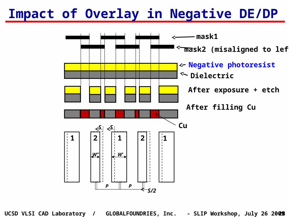
Impact of Overlay in Negative DE/DP
1 2 1 2 1
W’’ W’
P P
S S
S/2
mask1
mask2 (misaligned to left)
Negative photoresist
Dielectric
After exposure + etch
After filling Cu
Cu

29UCSD VLSI CAD Laboratory / GLOBALFOUNDRIES, Inc. - SLIP Workshop, July 26 2009
Impact of Overlay in Positive SDP
1 2 1 2 1
WW’’
P P
S S
Primary patterns
Dielectric
After exposure + etch
After filling Cu
Spacers (act as if masks)
(kind of) Positive photoresist
Cu

30UCSD VLSI CAD Laboratory / GLOBALFOUNDRIES, Inc. - SLIP Workshop, July 26 2009
Impact of Overlay in Positive SDP
1 2 1 2 1
W’ W’
P’’ P’
S S
Primary patterns
Dielectric
After exposure + etch
After filling Cu
Spacers (act as if masks)
(kind of ) Negative photoresist
Cu

31UCSD VLSI CAD Laboratory / GLOBALFOUNDRIES, Inc. - SLIP Workshop, July 26 2009
• Overlay error can cause more than +/- 10% capacitance variation within a die
This variation must be back-annotated to timing analysis to reduce unnecessary guardbanding
Ca
pac
ita
nc
e V
ari
ati
on
(%
)
Electrical Impacts: Capacitance Variation

32UCSD VLSI CAD Laboratory / GLOBALFOUNDRIES, Inc. - SLIP Workshop, July 26 2009
P-DE/DP N-DE/DP P-SDP N-SDP
M2
M4
|S|/2|S| |S|/2 |S|/2
|S| |S|/2 |S|/2 |S|/2

33UCSD VLSI CAD Laboratory / GLOBALFOUNDRIES, Inc. - SLIP Workshop, July 26 2009
• A net has maximum crosstalk-induced delay• SDP shows more sensitivity tighten overlay spec• P-DE/DP shows least sensitivity lessen overlay spec
Maximum Crosstalk Induced Delay
P-DE/DP N-DE/DP P-SDP N-SDP
M4
|S| |S|/2 |S|/2 |S|/2
M2 M4 M2 M4
w/o metal fill w/ metal fill

34UCSD VLSI CAD Laboratory / GLOBALFOUNDRIES, Inc. - SLIP Workshop, July 26 2009
Total Negative Slack Variation• SDP, especially for lower layer (smaller feature),
shows more sensitivity tighter overlay spec
0%
2%
4%
6%
8%
10%
12%
1 2 3
TN
S V
ari
ati
on
(%
)
Overlay error S variation (sigma)
P-DE/DP M2 P-DE/DP M3 P-DE/DP M4 P-DE/DP M5N-DE/DP M2 N-DE/DP M3 N-DE/DP M4 N-DE/DP M5P-SDP M2 P-SDP M3 P-SDP M4 P-SDP M5N-SDP M2 N-SDP M3 N-SDP M4 N-SDP M5
P-SDP
N-SDPM2
M4