Embed Size (px)
Citation preview

1FEATURES DESCRIPTION
APPLICATIONS
OFFSET VOLTAGE
vs COMMON-MODE VOLTAGE
(V = 1.8V)S
Common-Mode Voltage (V)
Off
se
t V
olta
ge
0 0.2 0.4 0.6 0.8 1.0 1.2 1.4 1.6 1.8
Competition
OPA369
OPA369OPA2369
www.ti.com ............................................................................................................................................ SBOS414B–AUGUST 2007–REVISED DECEMBER 2008
1.8V, 700nA, Zerø-CrossoverRAIL-TO-RAIL I/O OPERATIONAL AMPLIFIER
2• nanoPOWER: The OPA369 and OPA2369 are ultra-low-power,low-voltage operational amplifiers from Texas– OPA369: 800nAInstruments designed especially for battery-powered– OPA2369: 700nA/ch.applications.
• LOW OFFSET VOLTAGE: 250µVThe OPAx369 operates on a supply voltage as low as– ZERO-CROSSOVER 1.8V and has true rail-to-rail operation that makes it
• LOW OFFSET DRIFT: 0.4µV/°C useful for a wide range of applications. Thezerø-crossover feature resolves the problem of input• DC PRECISION:crossover distortion that becomes very prominent in– CMRR: 114dBlow voltage (< 3V), rail-to-rail input applications.
– PSRR:106dBIn addition to microsize packages and very low– AOL: 134dB quiescent current, the OPAx369 features 12kHz
• GAIN-BANDWIDTH PRODUCT: 12kHz bandwidth, low offset drift (1.75µV/°C, max), and lownoise 3.6µVPP (0.1Hz to 10Hz).• SUPPLY VOLTAGE: 1.8V to 5.5V
• microSIZE PACKAGES: The OPA369 (single version) is offered in an SC70-5package. The OPA2369 (dual version) comes in both– SC70-5, SOT23-5, MSOP-8MSOP-8 and SOT23-8 packages.
hi laurie
• BATTERY-POWERED INSTRUMENTS• PORTABLE DEVICES• MEDICAL INSTRUMENTS• TEST EQUIPMENT• LOW-POWER SENSOR SIGNAL
CONDITIONING
1
Please be aware that an important notice concerning availability, standard warranty, and use in critical applications of TexasInstruments semiconductor products and disclaimers thereto appears at the end of this data sheet.
2All trademarks are the property of their respective owners.
PRODUCTION DATA information is current as of publication date. Copyright © 2007–2008, Texas Instruments IncorporatedProducts conform to specifications per the terms of the TexasInstruments standard warranty. Production processing does notnecessarily include testing of all parameters.
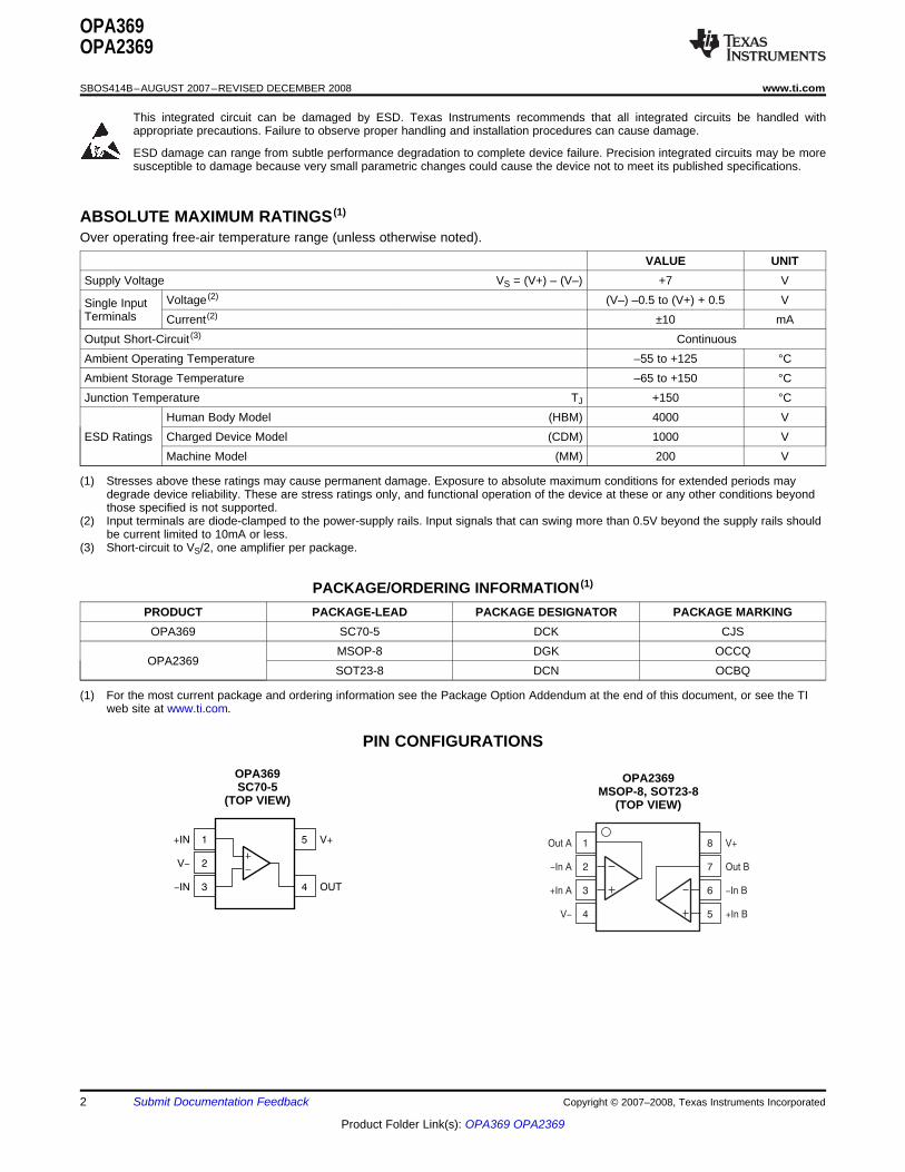
ABSOLUTE MAXIMUM RATINGS (1)
PIN CONFIGURATIONS
1
2
3
5
4
V+
OUT
+IN
V-
-IN
1
2
3
4
8
7
6
5
V+
Out B
-In B
+In B
Out A
-In A
+In A
V-
OPA369OPA2369
SBOS414B–AUGUST 2007–REVISED DECEMBER 2008 ............................................................................................................................................ www.ti.com
This integrated circuit can be damaged by ESD. Texas Instruments recommends that all integrated circuits be handled withappropriate precautions. Failure to observe proper handling and installation procedures can cause damage.
ESD damage can range from subtle performance degradation to complete device failure. Precision integrated circuits may be moresusceptible to damage because very small parametric changes could cause the device not to meet its published specifications.
Over operating free-air temperature range (unless otherwise noted).
VALUE UNITSupply Voltage VS = (V+) – (V–) +7 V
Voltage (2) (V–) –0.5 to (V+) + 0.5 VSingle InputTerminals Current (2) ±10 mAOutput Short-Circuit (3) ContinuousAmbient Operating Temperature –55 to +125 °CAmbient Storage Temperature –65 to +150 °CJunction Temperature TJ +150 °C
Human Body Model (HBM) 4000 VESD Ratings Charged Device Model (CDM) 1000 V
Machine Model (MM) 200 V
(1) Stresses above these ratings may cause permanent damage. Exposure to absolute maximum conditions for extended periods maydegrade device reliability. These are stress ratings only, and functional operation of the device at these or any other conditions beyondthose specified is not supported.
(2) Input terminals are diode-clamped to the power-supply rails. Input signals that can swing more than 0.5V beyond the supply rails shouldbe current limited to 10mA or less.
(3) Short-circuit to VS/2, one amplifier per package.
PACKAGE/ORDERING INFORMATION (1)
PRODUCT PACKAGE-LEAD PACKAGE DESIGNATOR PACKAGE MARKINGOPA369 SC70-5 DCK CJS
MSOP-8 DGK OCCQOPA2369
SOT23-8 DCN OCBQ
(1) For the most current package and ordering information see the Package Option Addendum at the end of this document, or see the TIweb site at www.ti.com.
OPA369 OPA2369SC70-5 MSOP-8, SOT23-8
(TOP VIEW) (TOP VIEW)
2 Submit Documentation Feedback Copyright © 2007–2008, Texas Instruments Incorporated
Product Folder Link(s): OPA369 OPA2369

ELECTRICAL CHARACTERISTICS: VS = +1.8V to +5.5V
OPA369OPA2369
www.ti.com ............................................................................................................................................ SBOS414B–AUGUST 2007–REVISED DECEMBER 2008
BOLDFACE limits apply over the specified temperature range, TA = –40°C to +85°C.At TA = +25°C, and RL = 100kΩ connected to VS/2, unless otherwise noted.
OPA369, OPA2369
PARAMETER CONDITIONS MIN TYP MAX UNIT
OFFSET VOLTAGE
Input Offset Voltage VOS 250 750 µV
over Temperature 1 mV
Drift dVOS/dT 0.4 1.75 µV/°C
vs Power Supply PSRR VS = 1.8V to 5.5V 5 20 µV/V
Channel Separation dc 140 dB
f = 1kHz 120 dB
INPUT VOLTAGE RANGE
Common-Mode Voltage Range VCM (V–) (V+) V
Common-Mode Rejection Ratio CMRR (V–) ≤ VCM ≤ (V+) 100 114 dB
over Temperature (V–) ≤ VCM ≤ (V+) 90 dB
INPUT BIAS CURRENT
Input Bias Current IB 10 50 pA
over Temperature See Figure 16 pA
Input Offset Current IOS 10 50 pA
INPUT IMPEDANCE
Differential Ω || pF1013|| 3
Common-Mode Ω || pF1013|| 6
NOISE
Input Voltage Noise f = 0.1Hz to 10Hz 3.6 µVPP
Input Voltage Noise Density f = 100Hz 220 nV/√Hz
f = 1kHz 290 nV/√Hz
Current Noise Density f = 1kHz 1 fA/√Hz
OPEN-LOOP GAIN
Open-Loop Voltage Gain AOL 100mV ≤ VO ≤ (V+)–100mV, 114 134 dBRL = 100kΩ
Over Temperature 100mV ≤ VO ≤ (V+)–100mV, 100 dBRL = 100kΩ
500mV ≤ VO ≤ (V+)–500mV, 114 134 dBRL = 10kΩ
Over Temperature 500mV ≤ VO ≤ (V+)–500mV, 90 dBRL = 10kΩ
OUTPUT
Voltage Output Swing from Rail RL = 100kΩ 10 mV
RL = 10kΩ 25 mV
Short-Circuit Current ISC 10 mA
Capacitive Load Drive CLOAD See Figure 20 pF
FREQUENCY RESPONSE
Gain-Bandwidth Product GBW 12 kHz
Slew Rate SR G = +1 0.005 V/µs
Overload Recovery Time VIN × Gain > VS 250 µs
Copyright © 2007–2008, Texas Instruments Incorporated Submit Documentation Feedback 3
Product Folder Link(s): OPA369 OPA2369

OPA369OPA2369
SBOS414B–AUGUST 2007–REVISED DECEMBER 2008 ............................................................................................................................................ www.ti.com
ELECTRICAL CHARACTERISTICS: VS = +1.8V to +5.5V (continued)BOLDFACE limits apply over the specified temperature range, TA = –40°C to +85°C.At TA = +25°C, and RL = 100kΩ connected to VS/2, unless otherwise noted.
OPA369, OPA2369
PARAMETER CONDITIONS MIN TYP MAX UNIT
POWER SUPPLY
Specified Voltage VS 1.8 5.5 V
Quiescent Current IQ IOUT = 0A
OPA369 0.8 1.2 µA
OPA2369 (per channel) 0.7 1 µA
Over Temperature
OPA369 1.45 µA
OPA2369 (per channel) 1.25 µA
TEMPERATURE RANGE
Specified Range TA –40 +85 °C
Operating Range TA –55 +125 °C
Thermal Resistance θ JA
SC70 250 °C/W
SOT23 223 °C/W
MSOP 252 °C/W
4 Submit Documentation Feedback Copyright © 2007–2008, Texas Instruments Incorporated
Product Folder Link(s): OPA369 OPA2369
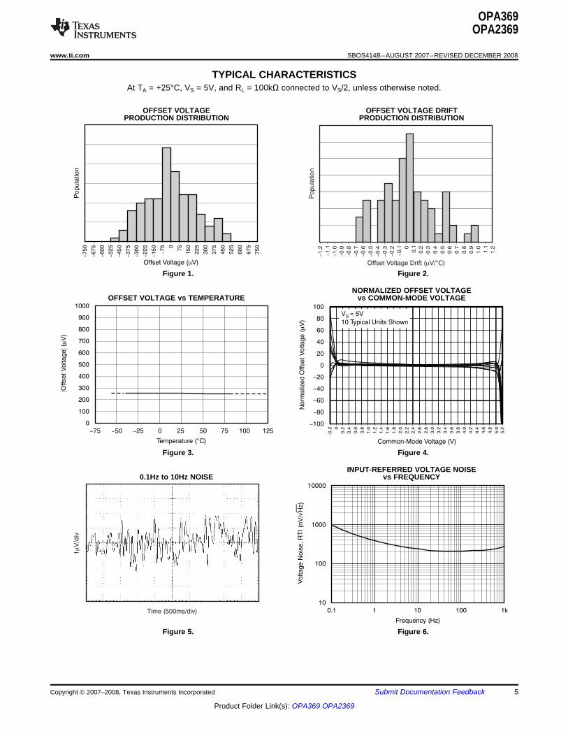
TYPICAL CHARACTERISTICSP
opula
tion
Offset Voltage ( V)m
-750
-675
-600
-525
-450
-375
-300
-225
-150
-75 0
75
150
225
300
375
450
525
600
675
750
-1.2
Po
pu
latio
n
Offset Voltage Drift ( V/ C)m °
-1.1
-1.0
-0.9
-0.8
-0.7
-0.6
-0.5
-0.4
-0.3
-0.2
-0.1 0
0.1
0.2
0.3
0.4
0.5
0.6
0.7
0.8
0.9
1.0 1.1
1.2
1000
900
800
700
600
500
400
300
200
100
0
Temperature ( C)°
||
Off
se
t V
olta
ge
(V
)m
-75 100 125-50 -25 0 25 50 75
Norm
aliz
ed
Offset V
oltage
m(V
)100
80
60
40
20
0
-20
-40
-60
-80
-100
Common-Mode Voltage (V)
-0
.2 0
0.2
0.4
0.6
0.8
1.0
1.2
1.4
1.6
1.8
2.0
2.2
2.4
2.6
2.8
3.0
3.2
3.4
3.6
3.8
4.0
4.2
4.4
4.6
4.8
5.0
5.2
V = 5VS
10 Typical Units Shown
1m
V/d
iv
Time (500ms/div)
10000
1000
100
10
Frequency (Hz)
Voltage N
ois
e, R
TI (n
V/
)ÖH
z
0.1 100101 1k
OPA369OPA2369
www.ti.com ............................................................................................................................................ SBOS414B–AUGUST 2007–REVISED DECEMBER 2008
At TA = +25°C, VS = 5V, and RL = 100kΩ connected to VS/2, unless otherwise noted.
OFFSET VOLTAGE OFFSET VOLTAGE DRIFTPRODUCTION DISTRIBUTION PRODUCTION DISTRIBUTION
Figure 1. Figure 2.
NORMALIZED OFFSET VOLTAGEOFFSET VOLTAGE vs TEMPERATURE vs COMMON-MODE VOLTAGE
Figure 3. Figure 4.
INPUT-REFERRED VOLTAGE NOISE0.1Hz to 10Hz NOISE vs FREQUENCY
Figure 5. Figure 6.
Copyright © 2007–2008, Texas Instruments Incorporated Submit Documentation Feedback 5
Product Folder Link(s): OPA369 OPA2369

3.0
2.5
2.0
1.5
1.0
0.5
0
Temperature ( C)°
A(
V/V
)m
OL
-75 -50 -25 0 25 50 75 100 125
R = 10kWL
R = 100kWL
140
120
100
80
60
40
20
0
-20
Frequency (Hz)
Gain
(dB
)
0.001 100 1k100.1 10.01 20k10k
PHASE
GAIN
180
135
90
45
0
Phase (
)°
120
100
80
60
40
20
0
Frequency (Hz)
CM
RR
(dB
)
10 10k1k100 20k
10
8
6
4
2
0
Temperature ( C)°
CM
RR
(V
/V)
m
-75 100 125-50 -25 0 25 50 75
20
15
10
5
0
-5
-10
-15
-20
Temperature ( C)°
PS
RR
(V
/V)
m
-75 -50 -25 0 25 50 75 100 125
10 Typical Units Shown110
100
90
80
70
60
50
40
30
20
10
0
Frequency (Hz)
PS
RR
(dB
)
1 1k 10k10010 20k
+PSRR
-PSRR
OPA369OPA2369
SBOS414B–AUGUST 2007–REVISED DECEMBER 2008 ............................................................................................................................................ www.ti.com
TYPICAL CHARACTERISTICS (continued)At TA = +25°C, VS = 5V, and RL = 100kΩ connected to VS/2, unless otherwise noted.
OPEN-LOOP GAIN AND PHASEvs FREQUENCY OPEN-LOOP GAIN vs TEMPERATURE
Figure 7. Figure 8.
COMMON-MODE REJECTION RATIO COMMON-MODE REJECTION RATIOvs FREQUENCY vs TEMPERATURE
Figure 9. Figure 10.
POWER-SUPPLY REJECTION RATIO POWER-SUPPLY REJECTION RATIOvs FREQUENCY vs TEMPERATURE
Figure 11. Figure 12.
6 Submit Documentation Feedback Copyright © 2007–2008, Texas Instruments Incorporated
Product Folder Link(s): OPA369 OPA2369

25
20
15
10
5
0
-5
-10
-15
-20
-25
Temperature ( C)°
Outp
ut V
oltage S
win
g-f
rom
-Rail
(mV
)
-75 100 125-50 -25 0 25 50 75
R = 10kWL
R = 100kWL
R = 100kWL
R = 10kWL
Outp
ut V
oltage (
V)
0
2.75
2.25
1.75
1.25
0.75
0.25
-0.25
-0.75
-1.25
-1.75
-2.25
-2.75
Output Current (mA)
455 3010 15 20 25 35 40
+115 C°
+85 C° +25 C° -40°C
V = 2.75VS ±
3.0
2.5
2.0
1.5
1.0
0.5
0
Frequency (Hz)
Maxim
um
V(V
)O
UT
100 1k 2k
Input B
ias C
urr
ent (p
A)
-50
10k
1k
100
10
1
0.1
0.01
Temperature ( C)°
125-25 0 25 50 75 100
2.5
2.0
1.5
1.0
0.5
Temperature ( C)°
Quie
scent C
urr
ent (
A)
m
-75 100-50 -25 0 25 50 75 125
Dual
Single
10M
1M
100k
10k
1k
100
10
Frequency (Hz)
0 1M10
Z(
)W
O
100 1k 10k 100k
OPA369OPA2369
www.ti.com ............................................................................................................................................ SBOS414B–AUGUST 2007–REVISED DECEMBER 2008
TYPICAL CHARACTERISTICS (continued)At TA = +25°C, VS = 5V, and RL = 100kΩ connected to VS/2, unless otherwise noted.
OUTPUT VOLTAGE OUTPUT VOLTAGE SWING-FROM-RAILvs OUTPUT CURRENT vs TEMPERATURE
Figure 13. Figure 14.
MAXIMUM OUTPUT VOLTAGE INPUT BIAS CURRENTvs FREQUENCY vs TEMPERATURE
Figure 15. Figure 16.
OPEN-LOOP OUTPUT IMPEDANCEQUIESCENT CURRENT vs TEMPERATURE vs FREQUENCY
Figure 17. Figure 18.
Copyright © 2007–2008, Texas Instruments Incorporated Submit Documentation Feedback 7
Product Folder Link(s): OPA369 OPA2369

160
140
120
100
80
60
40
20
0
Frequency (Hz)
Channel S
epara
tion (
dB
)
100 10k1k 100k
20
18
16
14
12
10
8
6
4
2
0
Capacitive Load (pF)
Overs
hoot (%
)
10 100
G = +1
G = 1-
20m
V/d
iv
Time (100 s/div)m
C = 20pFL500m
V/d
iv
Time (250 s/div)m
1V
/div
Time (500 s/div)m
Input
Output
OPA369OPA2369
SBOS414B–AUGUST 2007–REVISED DECEMBER 2008 ............................................................................................................................................ www.ti.com
TYPICAL CHARACTERISTICS (continued)At TA = +25°C, VS = 5V, and RL = 100kΩ connected to VS/2, unless otherwise noted.
SMALL-SIGNAL OVERSHOOTCHANNEL SEPARATION vs FREQUENCY vs CAPACITIVE LOAD
Figure 19. Figure 20.
SMALL-SIGNAL STEP RESPONSE LARGE-SIGNAL STEP RESPONSE
Figure 21. Figure 22.
OVERLOAD RECOVERY
Figure 23.
8 Submit Documentation Feedback Copyright © 2007–2008, Texas Instruments Incorporated
Product Folder Link(s): OPA369 OPA2369

APPLICATION INFORMATION
PROTECTING INPUTS FROM
OPERATING VOLTAGE
5kW
OPA36910mA max
VS
VIN
VOUT
IOVERLOAD
Current-limiting resistor
required if input voltage
exceeds supply rails by
³ 0.5V.
INPUT COMMON-MODE VOLTAGE RANGE
OPA369OPA2369
www.ti.com ............................................................................................................................................ SBOS414B–AUGUST 2007–REVISED DECEMBER 2008
The OPA369 family of operational amplifiers The input common-mode voltage range of theminimizes power consumption and operates on OPA369 family typically extends to each supply rail.supply voltages as low as 1.8V. Power-supply CMRR is specified from the negative rail to therejection ratio (PSRR), common-mode rejection ratio positive rail. See Figure 4, Normalized Offset Voltage(CMRR), and open-loop gain (AOL) typical values are vs Common-Mode Voltage.in the range of 100dB or better.
When designing for ultralow power, choose system OVER-VOLTAGEcomponents carefully. To minimize currentconsumption, select large-value resistors. Any Input currents are typically 10pA. However, largeresistors will react with stray capacitance in the circuit inputs (greater than 500mV beyond the supply rails)and the input capacitance of the operational amplifier. can cause excessive current to flow in or out of theThese parasitic RC combinations can affect the input pins. Therefore, in addition to keeping the inputstability of the overall system. A feedback capacitor voltage between the supply rails, it is also importantmay be required to assure stability and limit to limit the input current to less than 10mA. Thisovershoot or gain peaking. limiting is easily accomplished with an input resistor,
as shown in Figure 24.Good layout practice mandates the use of a 0.1µFbypass capacitor placed closely across the supplypins.
OPA369 series op amps are fully specified and testedfrom +1.8V to +5.5V (±0.9V to ±2.75V). Parametersthat vary significantly with supply voltage are shownin the Typical Characteristic curves.
Figure 24. Input Current Protection for VoltagesThe OPA369 family is designed to eliminate the input Exceeding the Supply Voltageoffset transition region typically present in mostrail-to-rail complementary stage operationalamplifiers, which allows the OPA369 family ofamplifiers to provide superior common-modeperformance over the entire input range.
Copyright © 2007–2008, Texas Instruments Incorporated Submit Documentation Feedback 9
Product Folder Link(s): OPA369 OPA2369

BATTERY MONITORINGR = R
1 F= 20MW
VHYST
VBATT
= 420kW50mV
2.4V (2)
R =2
-V
THRS
V1REF
R´1
R1
1
( ) - 1
RF
=
-2V
1.2V 420kW´1
420kW
1
( ) - 1
20MW
= 650kW (3)
R =F
VREF
1000(IBMAX
)
= 1.2V1000(50pA)
= 24M 20MW W» (1)
R =BIAS
= 0.3MW(V
BATTMIN- V )
REF
IBIAS
=( 1.2V)-1.8V
2 Am (4)
REF1112
OPA369
+IN
OUT
-INV
STATUSVBATT
VREF
R1
R2
RBIAS
IBIAS
RF
+
OPA369OPA2369
SBOS414B–AUGUST 2007–REVISED DECEMBER 2008 ............................................................................................................................................ www.ti.com
The low operating voltage and quiescent current ofthe OPA369 series make it an excellent choice for
4. Select a threshold voltage for VIN rising (VTHRS) =battery monitoring applications, as shown in2.0VFigure 25. In this circuit, VSTATUS is high as long as
5. Calculate R2 as follows:the battery voltage remains above 2V. A low-powerreference is used to set the trip point. Resistor valuesare selected as follows:
1. Selecting RF: Select RF such that the currentthrough RF is approximately 1000x larger thanthe maximum bias current over temperature:
6. Calculate RBIAS: The minimum supply voltage forthis circuit is 1.8V. The REF1112 has a currentrequirement of 1.2µA (max). Providing the2. Choose the hysteresis voltage, VHYST. ForREF1112 with 2µA of supply current assuresbattery-monitoring applications, 50mV isproper operation. Therefore:adequate.
3. Calculate R1 as follows:
Figure 25. Battery Monitor
10 Submit Documentation Feedback Copyright © 2007–2008, Texas Instruments Incorporated
Product Folder Link(s): OPA369 OPA2369

WINDOW COMPARATOR
V =H
R2
R + R1 2
´ VS
(5)
V =L
R4
R + R3 4
´ VS
(6)
VS
A1
A2
D1(2)
D2(2)
R5
10kW
R6
5.1kW
R7
5.1kW
RIN
2kW(1)
VS
VS
Q1(3)
R1
VH
VL
R2
1/2
OPA2369
1/2
OPA2369
VS
VOUT
VIN
VS
R3
R4
NOTES: (1) R protects A1 and A2 from possible excess current flow.IN
(2) IN4446 or equivalent diodes.
(3) 2N2222 or equivalent NPN transistor.
OPA369OPA2369
www.ti.com ............................................................................................................................................ SBOS414B–AUGUST 2007–REVISED DECEMBER 2008
If VIN falls below VL, the output of A2 is high, currentflows through D2, and VOUT is low. Likewise, if VINFigure 26 shows the OPA2369 used as a window rises above VH, the output of A1 is high, current flowscomparator. The threshold limits are set by VH and through D1, and VOUT is low. The window comparatorVL, with VH > VL. When VIN < VH, the output of A1 is threshold voltages are set as follows:low. When VIN > VL, the output of A2 is low.
Therefore, both op amp outputs are at 0V as long asVIN is between VH and VL. This architecture results inno current flowing through either diode, Q1 in cutoff,with the base voltage at 0V, and VOUT forced high.
Figure 26. OPA2369 as a Window Comparator
Copyright © 2007–2008, Texas Instruments Incorporated Submit Documentation Feedback 11
Product Folder Link(s): OPA369 OPA2369

ADDITIONAL APPLICATION EXAMPLES
R1
VEX
VOUT
VREF
R1
OPA369
RR
R R
+5V
OPA369
Output
RSHUNT
Load
V+
RG
RL
R(2)
1
10kW
RBIAS
+5V
zener(1)
Two zener
biasing methods
are shown.(3)
MOSFET rated to
stand-off supply voltage
such as BSS84 for
up to 50V.
(1) Zener rated for op amp supply capability (that is, 5.1V for OPA369).
(2) Current-limiting resistor.
(3) Choose zener biasing resistor or dual NMOSFETs (FDG6301N, NTJD4001N, or Si1034)
NOTES:
V-
R2
V = (V - V ) 1 + + + VOUT 1 2 REF
R1
R2
RG
R2R1VREF VOUT
V2
V1
R1
1/2
OPA2369
1/2
OPA2369
2R1
RG
OPA369OPA2369
SBOS414B–AUGUST 2007–REVISED DECEMBER 2008 ............................................................................................................................................ www.ti.com
Figure 27 through Figure 29 illustrate additional application examples.
Figure 27. Single Op Amp Bridge Amplifier
Figure 28. High-Side Current Monitor
Figure 29. Two Op Amp Instrumentation Amplifier
12 Submit Documentation Feedback Copyright © 2007–2008, Texas Instruments Incorporated
Product Folder Link(s): OPA369 OPA2369

PACKAGE OPTION ADDENDUM
www.ti.com 12-Aug-2017
Addendum-Page 1
PACKAGING INFORMATION
Orderable Device Status(1)
Package Type PackageDrawing
Pins PackageQty
Eco Plan(2)
Lead/Ball Finish(6)
MSL Peak Temp(3)
Op Temp (°C) Device Marking(4/5)
Samples
OPA2369AIDCNR ACTIVE SOT-23 DCN 8 3000 Green (RoHS& no Sb/Br)
CU NIPDAU Level-2-260C-1 YEAR -40 to 85 OCBQ
OPA2369AIDCNRG4 ACTIVE SOT-23 DCN 8 3000 Green (RoHS& no Sb/Br)
CU NIPDAU Level-2-260C-1 YEAR -40 to 85 OCBQ
OPA2369AIDCNT ACTIVE SOT-23 DCN 8 250 Green (RoHS& no Sb/Br)
CU NIPDAU Level-2-260C-1 YEAR -40 to 85 OCBQ
OPA2369AIDCNTG4 ACTIVE SOT-23 DCN 8 250 Green (RoHS& no Sb/Br)
CU NIPDAU Level-2-260C-1 YEAR -40 to 85 OCBQ
OPA2369AIDGKR ACTIVE VSSOP DGK 8 2500 Green (RoHS& no Sb/Br)
CU NIPDAU |CU NIPDAUAG
Level-2-260C-1 YEAR -40 to 85 OCCQ
OPA2369AIDGKT ACTIVE VSSOP DGK 8 250 Green (RoHS& no Sb/Br)
CU NIPDAU |CU NIPDAUAG
Level-2-260C-1 YEAR -40 to 85 OCCQ
OPA2369AIDGKTG4 ACTIVE VSSOP DGK 8 250 Green (RoHS& no Sb/Br)
CU NIPDAUAG Level-2-260C-1 YEAR -40 to 85 OCCQ
OPA369AIDCKR ACTIVE SC70 DCK 5 3000 Green (RoHS& no Sb/Br)
CU NIPDAU Level-2-260C-1 YEAR -40 to 85 CJS
OPA369AIDCKT ACTIVE SC70 DCK 5 250 Green (RoHS& no Sb/Br)
CU NIPDAU Level-2-260C-1 YEAR -40 to 85 CJS
(1) The marketing status values are defined as follows:ACTIVE: Product device recommended for new designs.LIFEBUY: TI has announced that the device will be discontinued, and a lifetime-buy period is in effect.NRND: Not recommended for new designs. Device is in production to support existing customers, but TI does not recommend using this part in a new design.PREVIEW: Device has been announced but is not in production. Samples may or may not be available.OBSOLETE: TI has discontinued the production of the device.
(2) RoHS: TI defines "RoHS" to mean semiconductor products that are compliant with the current EU RoHS requirements for all 10 RoHS substances, including the requirement that RoHS substancedo not exceed 0.1% by weight in homogeneous materials. Where designed to be soldered at high temperatures, "RoHS" products are suitable for use in specified lead-free processes. TI mayreference these types of products as "Pb-Free".RoHS Exempt: TI defines "RoHS Exempt" to mean products that contain lead but are compliant with EU RoHS pursuant to a specific EU RoHS exemption.Green: TI defines "Green" to mean the content of Chlorine (Cl) and Bromine (Br) based flame retardants meet JS709B low halogen requirements of <=1000ppm threshold. Antimony trioxide basedflame retardants must also meet the <=1000ppm threshold requirement.
(3) MSL, Peak Temp. - The Moisture Sensitivity Level rating according to the JEDEC industry standard classifications, and peak solder temperature.

PACKAGE OPTION ADDENDUM
www.ti.com 12-Aug-2017
Addendum-Page 2
(4) There may be additional marking, which relates to the logo, the lot trace code information, or the environmental category on the device.
(5) Multiple Device Markings will be inside parentheses. Only one Device Marking contained in parentheses and separated by a "~" will appear on a device. If a line is indented then it is a continuationof the previous line and the two combined represent the entire Device Marking for that device.
(6) Lead/Ball Finish - Orderable Devices may have multiple material finish options. Finish options are separated by a vertical ruled line. Lead/Ball Finish values may wrap to two lines if the finishvalue exceeds the maximum column width.
Important Information and Disclaimer:The information provided on this page represents TI's knowledge and belief as of the date that it is provided. TI bases its knowledge and belief on informationprovided by third parties, and makes no representation or warranty as to the accuracy of such information. Efforts are underway to better integrate information from third parties. TI has taken andcontinues to take reasonable steps to provide representative and accurate information but may not have conducted destructive testing or chemical analysis on incoming materials and chemicals.TI and TI suppliers consider certain information to be proprietary, and thus CAS numbers and other limited information may not be available for release.
In no event shall TI's liability arising out of such information exceed the total purchase price of the TI part(s) at issue in this document sold by TI to Customer on an annual basis.

TAPE AND REEL INFORMATION
*All dimensions are nominal
Device PackageType
PackageDrawing
Pins SPQ ReelDiameter
(mm)
ReelWidth
W1 (mm)
A0(mm)
B0(mm)
K0(mm)
P1(mm)
W(mm)
Pin1Quadrant
OPA2369AIDCNR SOT-23 DCN 8 3000 179.0 8.4 3.2 3.2 1.4 4.0 8.0 Q3
OPA2369AIDCNT SOT-23 DCN 8 250 179.0 8.4 3.2 3.2 1.4 4.0 8.0 Q3
OPA2369AIDGKR VSSOP DGK 8 2500 330.0 12.4 5.3 3.4 1.4 8.0 12.0 Q1
OPA2369AIDGKT VSSOP DGK 8 250 180.0 12.4 5.3 3.4 1.4 8.0 12.0 Q1
OPA369AIDCKR SC70 DCK 5 3000 179.0 8.4 2.2 2.5 1.2 4.0 8.0 Q3
OPA369AIDCKR SC70 DCK 5 3000 178.0 9.0 2.4 2.5 1.2 4.0 8.0 Q3
OPA369AIDCKT SC70 DCK 5 250 179.0 8.4 2.2 2.5 1.2 4.0 8.0 Q3
OPA369AIDCKT SC70 DCK 5 250 178.0 9.0 2.4 2.5 1.2 4.0 8.0 Q3
PACKAGE MATERIALS INFORMATION
www.ti.com 3-Aug-2017
Pack Materials-Page 1

*All dimensions are nominal
Device Package Type Package Drawing Pins SPQ Length (mm) Width (mm) Height (mm)
OPA2369AIDCNR SOT-23 DCN 8 3000 195.0 200.0 45.0
OPA2369AIDCNT SOT-23 DCN 8 250 195.0 200.0 45.0
OPA2369AIDGKR VSSOP DGK 8 2500 367.0 367.0 35.0
OPA2369AIDGKT VSSOP DGK 8 250 210.0 185.0 35.0
OPA369AIDCKR SC70 DCK 5 3000 195.0 200.0 45.0
OPA369AIDCKR SC70 DCK 5 3000 180.0 180.0 18.0
OPA369AIDCKT SC70 DCK 5 250 195.0 200.0 45.0
OPA369AIDCKT SC70 DCK 5 250 180.0 180.0 18.0
PACKAGE MATERIALS INFORMATION
www.ti.com 3-Aug-2017
Pack Materials-Page 2


IMPORTANT NOTICE
Texas Instruments Incorporated (TI) reserves the right to make corrections, enhancements, improvements and other changes to itssemiconductor products and services per JESD46, latest issue, and to discontinue any product or service per JESD48, latest issue. Buyersshould obtain the latest relevant information before placing orders and should verify that such information is current and complete.TI’s published terms of sale for semiconductor products (http://www.ti.com/sc/docs/stdterms.htm) apply to the sale of packaged integratedcircuit products that TI has qualified and released to market. Additional terms may apply to the use or sale of other types of TI products andservices.Reproduction of significant portions of TI information in TI data sheets is permissible only if reproduction is without alteration and isaccompanied by all associated warranties, conditions, limitations, and notices. TI is not responsible or liable for such reproduceddocumentation. Information of third parties may be subject to additional restrictions. Resale of TI products or services with statementsdifferent from or beyond the parameters stated by TI for that product or service voids all express and any implied warranties for theassociated TI product or service and is an unfair and deceptive business practice. TI is not responsible or liable for any such statements.Buyers and others who are developing systems that incorporate TI products (collectively, “Designers”) understand and agree that Designersremain responsible for using their independent analysis, evaluation and judgment in designing their applications and that Designers havefull and exclusive responsibility to assure the safety of Designers' applications and compliance of their applications (and of all TI productsused in or for Designers’ applications) with all applicable regulations, laws and other applicable requirements. Designer represents that, withrespect to their applications, Designer has all the necessary expertise to create and implement safeguards that (1) anticipate dangerousconsequences of failures, (2) monitor failures and their consequences, and (3) lessen the likelihood of failures that might cause harm andtake appropriate actions. Designer agrees that prior to using or distributing any applications that include TI products, Designer willthoroughly test such applications and the functionality of such TI products as used in such applications.TI’s provision of technical, application or other design advice, quality characterization, reliability data or other services or information,including, but not limited to, reference designs and materials relating to evaluation modules, (collectively, “TI Resources”) are intended toassist designers who are developing applications that incorporate TI products; by downloading, accessing or using TI Resources in anyway, Designer (individually or, if Designer is acting on behalf of a company, Designer’s company) agrees to use any particular TI Resourcesolely for this purpose and subject to the terms of this Notice.TI’s provision of TI Resources does not expand or otherwise alter TI’s applicable published warranties or warranty disclaimers for TIproducts, and no additional obligations or liabilities arise from TI providing such TI Resources. TI reserves the right to make corrections,enhancements, improvements and other changes to its TI Resources. TI has not conducted any testing other than that specificallydescribed in the published documentation for a particular TI Resource.Designer is authorized to use, copy and modify any individual TI Resource only in connection with the development of applications thatinclude the TI product(s) identified in such TI Resource. NO OTHER LICENSE, EXPRESS OR IMPLIED, BY ESTOPPEL OR OTHERWISETO ANY OTHER TI INTELLECTUAL PROPERTY RIGHT, AND NO LICENSE TO ANY TECHNOLOGY OR INTELLECTUAL PROPERTYRIGHT OF TI OR ANY THIRD PARTY IS GRANTED HEREIN, including but not limited to any patent right, copyright, mask work right, orother intellectual property right relating to any combination, machine, or process in which TI products or services are used. Informationregarding or referencing third-party products or services does not constitute a license to use such products or services, or a warranty orendorsement thereof. Use of TI Resources may require a license from a third party under the patents or other intellectual property of thethird party, or a license from TI under the patents or other intellectual property of TI.TI RESOURCES ARE PROVIDED “AS IS” AND WITH ALL FAULTS. TI DISCLAIMS ALL OTHER WARRANTIES ORREPRESENTATIONS, EXPRESS OR IMPLIED, REGARDING RESOURCES OR USE THEREOF, INCLUDING BUT NOT LIMITED TOACCURACY OR COMPLETENESS, TITLE, ANY EPIDEMIC FAILURE WARRANTY AND ANY IMPLIED WARRANTIES OFMERCHANTABILITY, FITNESS FOR A PARTICULAR PURPOSE, AND NON-INFRINGEMENT OF ANY THIRD PARTY INTELLECTUALPROPERTY RIGHTS. TI SHALL NOT BE LIABLE FOR AND SHALL NOT DEFEND OR INDEMNIFY DESIGNER AGAINST ANY CLAIM,INCLUDING BUT NOT LIMITED TO ANY INFRINGEMENT CLAIM THAT RELATES TO OR IS BASED ON ANY COMBINATION OFPRODUCTS EVEN IF DESCRIBED IN TI RESOURCES OR OTHERWISE. IN NO EVENT SHALL TI BE LIABLE FOR ANY ACTUAL,DIRECT, SPECIAL, COLLATERAL, INDIRECT, PUNITIVE, INCIDENTAL, CONSEQUENTIAL OR EXEMPLARY DAMAGES INCONNECTION WITH OR ARISING OUT OF TI RESOURCES OR USE THEREOF, AND REGARDLESS OF WHETHER TI HAS BEENADVISED OF THE POSSIBILITY OF SUCH DAMAGES.Unless TI has explicitly designated an individual product as meeting the requirements of a particular industry standard (e.g., ISO/TS 16949and ISO 26262), TI is not responsible for any failure to meet such industry standard requirements.Where TI specifically promotes products as facilitating functional safety or as compliant with industry functional safety standards, suchproducts are intended to help enable customers to design and create their own applications that meet applicable functional safety standardsand requirements. Using products in an application does not by itself establish any safety features in the application. Designers mustensure compliance with safety-related requirements and standards applicable to their applications. Designer may not use any TI products inlife-critical medical equipment unless authorized officers of the parties have executed a special contract specifically governing such use.Life-critical medical equipment is medical equipment where failure of such equipment would cause serious bodily injury or death (e.g., lifesupport, pacemakers, defibrillators, heart pumps, neurostimulators, and implantables). Such equipment includes, without limitation, allmedical devices identified by the U.S. Food and Drug Administration as Class III devices and equivalent classifications outside the U.S.TI may expressly designate certain products as completing a particular qualification (e.g., Q100, Military Grade, or Enhanced Product).Designers agree that it has the necessary expertise to select the product with the appropriate qualification designation for their applicationsand that proper product selection is at Designers’ own risk. Designers are solely responsible for compliance with all legal and regulatoryrequirements in connection with such selection.Designer will fully indemnify TI and its representatives against any damages, costs, losses, and/or liabilities arising out of Designer’s non-compliance with the terms and provisions of this Notice.
Mailing Address: Texas Instruments, Post Office Box 655303, Dallas, Texas 75265Copyright © 2017, Texas Instruments Incorporated


