Embed Size (px)
Citation preview

1878 JOURNAL OF MICROELECTROMECHANICAL SYSTEMS, VOL. 24, NO. 6, DECEMBER 2015
Pull-In Voltage and Fabrication Yield Analysis ofAll-Metal-Based Nanoelectromechanical Switches
You Qian, Student Member, IEEE, Bo Woon Soon, and Chengkuo Lee, Member, IEEE
Abstract— We designed a one-mask process forall-molybdenum-based laterally actuated nanoelectromechanicalswitches. The damascene-like process is designed to ensurea smooth, high-aspect ratio, and metal-to-metal mechanicalcontact. Based on the statistical study of 800 devices, very highprocess yield can be achieved for fixed–fixed beam devices byselecting suitable device dimensions, i.e., the beam length versusbeam width ratio should be <70 and the ratio of actuation gapto contact gap should be >1.5. Typical failure modes are alsodiscussed. [2014-0391]
Index Terms— Switches, nanoelectromechanical systems,electrostatic devices.
I. INTRODUCTION
ELECTROSTATICALLY actuated micro/nano electro-mechanical system (M/NEMS) switches have been
attracting attention for their excellent switching propertiesincluding zero-leakage current, abrupt switch behavior andpotential to operate in high temperature [1]–[5]. Theseunique properties make NEMS switch a strong candidate forultra-low power electronics and harsh environment integratedcircuit (IC) [6]–[10].
On the other hand, it would be difficult for NEMS switchesto entirely replace CMOS transistors in high performanceICs, since NEMS switches have lower a operating frequencydue to their large mechanical delay. To avoid the low speedNEMS switches slowing down the circuit and fully utilizetheir zero leakage properties, several applications have beenproposed for NEMS-CMOS integration, by using NEMSswitches to replace speed insensitive elements in fieldprogrammable gate array [11]–[15], power gating [16]–[18]and static random access memory [19]–[21]. Studies indicatethat introducing NEMS switches would largely reduce thepower consumption of the whole NEMS-CMOS IC. To realizehybrid NEMS-CMOS circuit [22], [23], directly fabricatingNEMS switches on top of CMOS layer would be a realisticand cost-effective technique. The semiconductor industryhas developed air gap back end process [24] which is mostsuitable for the NEMS-CMOS hybrid circuit.
Manuscript received December 26, 2014; revised May 10, 2015; acceptedJune 19, 2015. Date of publication July 15, 2015; date of current versionNovember 25, 2015. This work was supported in part by the Ministry ofEducation, Singapore, under Grant MOE2012-T2-2-154, and in part by theNational Research Foundation, Singapore, under Grant R-263-000-A27-281.Subject Editor C. T.-C. Nguyen.
The authors are with the Department of Electrical and ComputerEngineering, National University of Singapore, Singapore 117576, and alsowith the Center for Intelligent Sensors and Micro Electrical MechanicalSystems, National University of Singapore, Singapore 117576 (e-mail:[email protected]; [email protected]; [email protected]).
Color versions of one or more of the figures in this paper are availableonline at http://ieeexplore.ieee.org.
Digital Object Identifier 10.1109/JMEMS.2015.2449863
The following requirements should be fulfilled to enforceNEMS-CMOS integration: i) The NEMS switches should berealized by a low temperature CMOS-compatible process forthe ease of implementing the process in a modern CMOSfoundry; ii) A simple process is desired; especially whenit can leverage the existing metallization process; iii) Thetopography of the device should be small, to ensure the easyrealization of devices with multiple layers stacking and waferlevel encapsulation.
By far, most of NEMS switches are not suitable for theNEMS-CMOS integration. Many reports lack demonstrationof repeatable on/off switch behavior [2], [6], [25], while a fewreliable prototypes still need complicated processes to achieverobust structures. Yield of processes has not been addressedby recent studies [26]–[28]. All-metal based NEMS switchesseem to be a reasonable choice to align with post-CMOSprocess. Our preliminary study [29] shows that all-metal basedfixed-fixed beam NEMS switch has reliable performance evenunder accelerated high temperature measurement.
This work focuses on developing a robust, high processyield method for fabricating all-metal-based NEMS switch.It targets to achieve a single mask, CMOS compatibleprocess for NEMS-CMOS integration applications as well asNEMS-only logic circuits. It also includes a basic method forNEMS switch designers to quickly identify the pull-in voltageand suitable device dimension. Device fabrication yield andtypical failure modes are also discussed in the later section.
II. DESIGN CONSIDERATION
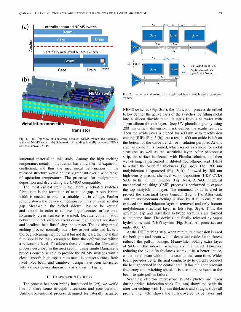
In this study, laterally actuated switches are chosen becausethey can be fabricated with a single mask process, withall terminals formed in a single etching step (Fig. 1(a)).In comparison, vertically actuated mechanical switches need4∼8 masks, multiple deposition and etching steps to assembleall terminals layer by layer. For three-dimensional integration,laterally actuated NEMS switches appear to have a muchsmaller topography, so that another layer of devices can beconveniently stacked on the existing device layer with asacrificial layer and vias in between (Fig. 1(b)) [13], [30]–[34].Since only one deposition step is involved in the laterallyactuated switch fabrication, metallic material is most favorablefor its low process temperature and low resistivity. As mostof the device failures happen in the contact area, includingwelding, material transfer, delamination, and destruction [35],metal of high hardness and high melting point are commonlyused, such as ruthenium [36]–[39], tungsten [40]–[42].
As a result, molybdenum, with high melting temperatureof 2623°C and relatively high hardness, is selected as the
1057-7157 © 2015 IEEE. Personal use is permitted, but republication/redistribution requires IEEE permission.See http://www.ieee.org/publications_standards/publications/rights/index.html for more information.
QIAN et al.: PULL-IN VOLTAGE AND FABRICATION YIELD ANALYSIS OF ALL-METAL-BASED NEMSs 1879
Fig. 1. (a) Top view of a laterally actuated NEMS switch and verticallyactuated NEMS switch. (b) Schematic of building laterally actuated NEMSswitches above CMOS.
structural material in this study. Among the high meltingtemperature metals, molybdenum has a low thermal expansioncoefficient, and thus the mechanical deformation of thereleased structure would be less significant over a wide rangeof operation temperature. The processes for molybdenumdeposition and dry etching are CMOS compatible.
The most critical step in the laterally actuated switchesfabrication is the formation of actuation gap. A sub 100nmwidth is needed to obtain a suitable pull-in voltage. Furtherscaling down the device dimension requires an even smallergap. Meanwhile, the etched sidewall has to be verticaland smooth in order to achieve larger contact surface area.Extremely clean surface is wanted, because contaminationbetween contact surfaces could cause high contact resistanceand localized heat flux fusing the contact. The existing metaletching process normally has a low aspect ratio and lacks athorough cleaning method. Last but not the least, the metal thinfilm should be thick enough to limit the deformation withina reasonable level. To address these concerns, the fabricationprocess described in the next section using single Damasceneprocess concept is able to provide the NEMS switches with aclean, smooth, high aspect ratio metallic contact surface. Bothfixed-fixed beam and cantilever design have been fabricatedwith various device dimensions as shown in Fig. 2.
III. FABRICATION PROCESS
The process has been briefly introduced in [29], we wouldlike to share some in-depth discussion and consideration.Unlike conventional process designed for laterally actuated
Fig. 2. Schematic drawing of a fixed-fixed beam switch and a cantileverswitch.
NEMS switches (Fig. 3(a)), the fabrication process describedbelow defines the active parts of the switches, by filling metalinto a silicon dioxide mold. It starts from a Si wafer with1 μm silicon dioxide layer. Deep UV photolithography using200 nm critical dimension mask defines the oxide features.Then the oxide layer is etched for 400 nm with reactive-ionetching (RIE) (Fig. 3 (b)). As a result, 600 nm oxide is left onthe bottom of the oxide trench for insulation purpose. At thisstep, an oxide fin is formed, which serves as a mold for metalstructures as well as the sacrificial layer. After photoresiststrip, the surface is cleaned with Piranha solution, and thenwet etching is performed in diluted hydrofluoric acid (DHF)to reduce the oxide fin thickness (Fig. 3(c)). Then 300 nmmolybdenum is sputtered (Fig. 3(d)), followed by 500 nmhigh-density plasma chemical vapor deposition (HDP CVD)SiO2 to fill all the trenches (Fig. 3(e)). A SiO2 chemicalmechanical polishing (CMP) process is performed to exposethe top molybdenum layer. The remained oxide is used toprotect the structural layer beneath (Fig. 3(f)). Afterward,300 nm molybdenum etching is done by RIE, to ensure theexposed top molybdenum layer is removed and only bottommolybdenum structural layer is left (Fig. 3(g)). Thus, theactuation gap and insulation between terminals are formedat the same time. The devices are finally released by vaporhydrofluoric acid (VHF) system (Fig. 3(h)). All processes areunder 400 °C.
At the DHF etching step, when minimum dimension is usedfor both gap and beam width, decreased oxide fin thicknessreduces the pull-in voltage. Meanwhile, adding extra layerof SiO2 on the sidewall achieves a similar effect. However,reducing the oxide fin thickness seems to be a better choice,as the metal beam width is increased at the same time. Widerbeam provides better thermal conductivity to quickly conductthe heat generated in the contact area. It has a higher resonantfrequency and switching speed. It is also more resistant to thebeam to gate pull-in failure.
Scanning electron microscope (SEM) photos are takenduring critical fabrication steps. Fig. 4(a) shows the oxide finafter wet etching with 100 nm thickness and straight sidewallprofile. Fig. 4(b) shows the fully-covered oxide layer and

1880 JOURNAL OF MICROELECTROMECHANICAL SYSTEMS, VOL. 24, NO. 6, DECEMBER 2015
Fig. 3. (a) The white dash line indicates the cross-section used in the following figures (b) SiO2 RIE forming the trench (c) Wet etch reducing the oxidefin thickness (d) 300nm molybdenum PVD (e) 500nm HDP CVD SiO2 (f) SiO2 CMP (g) molybdenum RIE (h) VHF release.
Fig. 4. SEM photos of devices near the contact region after (a) wet etch,(b) Mo deposition, (c) oxide CMP and (d) Mo RIE. (e) Whole device afterrelease. (f) Fixed-fixed beam pull-in by electron charging. (g) Test structureof a single beam. (h) Test structure of contact surface.
large grains on the surface after molybdenum PVD. Fig. 4(c)shows molybdenum on top of the oxide fin can be successfullyexposed after the oxide CMP step across the whole wafer.Fig. 4(d) shows the top molybdenum layer is etched away,and the upper edge of the oxide fin is exposed. Fig. 4(e)shows a released fixed-fixed beam device. Fig. 4(f) showsthe zoomed-in view of the contact area, where the beamis attracted to the drain terminal by accumulated electroncharges. The cantilever test structure (Fig. 4(g)) shows themolybdenum sidewall on the edges of the bottom molybdenumlayer is almost etched away. The smooth molybdenum sidewallprofile is shown in Fig. 4(h), where no visible grain can befound.
The differences between the proposed process above andconventional process are shown in table I. SiO2 insulationlayer and molybdenum structural layer are used in both cases.
TABLE I
PROCESS DIFFERENCES BETWEEN THIS WORK
AND CONVENTIONAL WORK
Although a few more steps are added, the proposed processshifts the formation of contact surface from molybdenumetching to deposition. The contact surface is not exposeduntil VHF release, which ensures etching residual do notcontaminate the surface. The back end process in CMOSfoundry could adapt this process easily with conventionaldual-Damascene process.
IV. ELECTRICAL MEASUREMENT OF A TYPICAL DEVICE
A typical fixed-fixed beam device is picked first to verifythe electrical performance. The measurement is conducted in avacuum wafer probing system (Cascade Microtech, PMV200,vacuum level: 5.4E-6 mbar) using a semiconductor parameteranalyzer (Agilent Technology, B1500A). It is first tested fordouble side I-V sweep with 500 nA current compliance.General NEMS switch behaviors, including abrupt switching,zero off-state current and hysteresis behavior can be foundin Fig. 5(a). Afterward, higher current in the drain terminalis tested, and an exceptionally high current of 1 mA isapplied with a 5s interval. The device shows a stable electricalperformance in Fig. 5(b) with an on/off ratio of 108.
The contact resistance of this device is also measuredwith 0.1V constant voltage at the drain terminal. The small

QIAN et al.: PULL-IN VOLTAGE AND FABRICATION YIELD ANALYSIS OF ALL-METAL-BASED NEMSs 1881
Fig. 5. Electrical tests for a fixed-fixed beam device with dimension of L B = 28 μm, t = 700 nm and gG B = 150 nm (a) I-V sweep with 500 nA currentcompliance. (b) Cycling test with 1 mA current applied on drain terminal. (c) Cycling test to obtain contact resistance. (d) Contact resistance change overthe cycling test.
drain voltage value is set to prevent the excessive currentto damage the contact. The current compliance is removedfrom this cycling test. Fig. 5(c) shows that in the initialcycle, the contact resistance is around 2.5 k�, indicating agood metal to metal contact. Fig. 5(d) reflects the contactresistance measured at every cycle. For the first 100 cycles,the gate voltage is set to be 28.5 V, the same as the measure-ment in Fig. 5(b) and (c). The contact resistance graduallyincreases and suddenly drops in the 56th cycle, and againthe resistance increases afterward. Then the gate voltage isincreased to 29.5V and 30.5V. The contact resistance hasa drop after voltage increases, and stabilizes at 5∼20 k�.After increasing the voltage to 31.5V, the beam collapses onthe gate terminal, causing the gate to beam shortage whichcannot be recovered afterward. The measurement indicatesthat a higher gate voltage helps to stabilize the contactresistance, but further improvement should be done by propersurface coating [43]–[45]. A long time accelerated reliabilitymeasurement can be found in [29]. A 28 μm long deviceis cycled for 28 hours under a 300°C environment withoutobvious performance degradation.
V. STATISTICAL STUDY ON PULL-IN VOLTAGE AND YEILD
After single device study, statistical measurement of pull-involtage and process yield have been carried by measuring800 devices, which includes 500 fixed-fixed beam NEMSswitches (50 different dimensions) and 300 cantilever beamswitches (30 different dimensions). These 800 devices arepicked from 5 different positions across the same wafer. Everychip contains two devices with identical dimension. Only twomost important factors, beam length and beam thickness vary,while other parameters are fixed. All parameter combinationsshown in table II are studied. Furthermore, for the fixed-fixedbeam, two addition parameters, the actuation gap, gG B , andthe contact gap, gD B, are also studied with two combinations.
Before electrical measurement, analytical solution and finiteelement modeling are performed to estimate the pull-in voltagefor each dimension. With simple parallel-plate model, pull-involtage of NEMS switch in vacuum is:
Vpi =√
8kef f g3G B
27ε0L Bw(1)
Where w is the thickness of the beam, ε0 is the permittivityof vacuum, kef f is the effective spring constant of the beam,
TABLE II
DESIGN PARAMETER
which is related to beam type and the electrostatic forcedistribution along the beam. For a more accurate kef f , weconsider the drain voltage is normally much smaller than thegate voltage, with no electrostatics force from drain terminalcontributed to the pull-in. For fixed-fixed beam cases, theelectrostatic force is missing in the middle of the beam.Thereby, the effective spring constant of the fixed-fixed beamis given by:
kef f = 4Ewt3
L2G(L B − LG)
(2)
Where E is the young’s modulus of molybdenum.The pull-in voltage of the fixed-fixed beam is given by:
Vpi =√
32Et3g3G B
27ε0L2G L B(L B − LG)
(3)
Similarly, for cantilever case, we consider no electrostaticforce at the tip of the beam:
kef f = 2Ewt3
L2G (4L B − LG)
(4)
The pull-in voltage is given by:
Vpi =√
16Et3g3G B
27ε0L2G L B(4L B − LG)
(5)
Notice the structure layer thickness has been cancelled dur-ing the calculation, therefore it does not have an impact on thepull-in voltage in this model. There are a lot of assumptions forthe parallel-plate model: a linear spring constant of the beam,

1882 JOURNAL OF MICROELECTROMECHANICAL SYSTEMS, VOL. 24, NO. 6, DECEMBER 2015
Fig. 6. Pull-in voltage summary of fixed-fixed beam devices withgG B = 150 nm, and gDB = 100 nm, with beam length L B , beam widtht varies.
a piston-like motion where pull-in always occurs whendeformation reaches one-third of the actuation gap, no fringingfield taken into account. 2D and 3D simulations are performedfor higher accuracy, using COMSOL Multiphysics tool [46].The 2D model covers a very wide range of dimension, and weonly did 3D simulations of the dimensions shown in Table II.The simulation sweeps the voltage from a smaller guessedvalue until convergence failure near the pull-in, and then thisvoltage is recorded as pull-in voltage. The simulation generallytakes quite a lot computational cost: one 2D simulation takes afew minutes, while 3D simulation needs tens of minutes usinga state-of-art workstation.
The simulation results have been plotted in Fig. 6-8.Where Fig 6 is fixed-fixed beam device with gD B=100 nm,gG B=150 nm. Fig 7 is also fixed-fixed beam device, but withgD B=150 nm, gG B=200 nm, Fig 8 is the cantilever devicewith gD B=100 nm, gG B=150 nm. The 3D simulation resultsare typically 10% lower than the 2D simulation, which ismost likely caused by the fringing field out-of-plane. Althoughso many assumptions are applied to the analytical solution,it appears that by simply adding a constant coefficient to
Fig. 7. Pull-in voltage summary of fixed-fixed beam devices withgG B = 200 nm, and gDB = 150 nm, with beam length L B , beam widtht varies.
equation (3) and (5), the analytical solution would fit the2D simulation very well.
For fixed-fixed beam:
Vpi = a f f
√32Et3g3
G B
27ε0L2G L B(L B − LG)
(6)
For cantilever beam:
Vpi = ac
√16Et3g3
G B
27ε0L2G L B(4L B − LG)
(7)
By assigning a f f = 1.26 and ac = 1.4, the deviationbetween analytical solution and 2D simulation is only ±2%for fixed-fixed beam and ±4.5% for cantilever across thewhole simulation range. For 3D simulation cases, assigninga f f = 1.2 and ac = 1.3, the deviation still reaches 10% insome cases. The accuracy of the analytical model is higherwhen L B/t is smaller than 70, with ±4% for fixed-fixed beamand ±5% for cantilevers. Although the equation is constrainedto a limited range, it is still acceptable as very high beamlength to width ratio is not desired in actual design, whichwill be discussed later.

QIAN et al.: PULL-IN VOLTAGE AND FABRICATION YIELD ANALYSIS OF ALL-METAL-BASED NEMSs 1883
Fig. 8. Pull-in voltage summary of cantilever beam devices withgG B = 150 nm, and gDB = 100 nm, with beam length L B , beam widtht varies.
With the prediction of the pull-in voltage, 800 devicesare measured individually. The procedures are as follows:an I-V sweep starts from 0V with 0.1V step. 10 nA complianceis given to each terminal. Current from every terminal ismonitored. Once pull-in phenomenon is observed, the I-Vsweep would be terminated manually, and typically the devicewould be overdriven for 1V. Based on the measurement, wecan classify the 800 measurements into 6 different categoriesbelow:
i. Repeatable devices: after the I-V sweep, a repeatabledevice shows beam current and drain current in the oppositedirection. The gate current keeps at noise level as shownin Fig. 9(a). A quick cycling test (for around 100 cycles) shownin Fig. 9(b) verifies the repeatability. ii. Gate to beam pull-in:in I-V sweep, the gate current raises at the same time with thebeam current or drain current as shown in Fig. 9(c), no cyclingbehavior can be observed in these devices. iii. Secondarypull-in: in the I-V sweep, the devices behave like the repeatabledevices at first, but they quickly show the gate to beam pull-inright after the first pull-in as shown in Fig. 9(d). iv. Stiction:in I-V sweep, the signal is identical to the repeatable devicesshown in Fig. 9(e). But in the following cycling measurement
Fig. 9. (a) I-V curve of a repeatable device (b) cycling measurement ofa repeatable device. (c) I-V curve of a gate to beam pull-in device. (d) I-Vcurve of a device to secondary pull-in. (e) First round I-V curve of a devicewith stiction (f) Second round I-V curve of a device with stiction.
Fig. 10. (a) beam deflection of a 60 μm fixed-fixed beam. (b) beam deflectionof a 50 μm cantilever.
and I-V sweep as shown in Fig. 9(f), the devices have constantcurrent between drain and beam even with 0V gate voltageapplied. v. Short circuit: in I-V sweep, the drain currentand beam current appear from the beginning of the sweep.vi. No signal: even after very large voltage overdrive, there isno current observed in any of the terminals.
Detailed causes of the failure will be discussed later.We focus on the pull-in voltage analysis first. In the above6 cases, pull-in voltage can be obtained from case 1 to case 4.All pull-in voltage data have been plotted in Fig 6∼8, thenumber besides the measurement data show the quantity ofthe data.
Generally the measured pull-in voltages for fixed-fixedbeam NEMS switches are smaller than simulation when beamlength is smaller than 60 μm. In Fig 4(f), (g) and (h),an extra sidewall exists on every edge, which will induce anextra electrostatic force. On the other hand, when the beamlength is larger than 60 μm, the pull-in voltage is muchhigher than expected. The test structure is checked undera holographic microscope (Lyncee Tec, DHM-R2200). Fora 60 μm fixed-fixed beam, the maximum deflection in themiddle is about 200 nm as shown in Fig. 10(a), therefore, theeffective capacitance between gate terminal and beam terminalis much smaller.
For cantilever case, the problem becomes severe, as the teststructure has a deflection of more than 300 nm at the point,

1884 JOURNAL OF MICROELECTROMECHANICAL SYSTEMS, VOL. 24, NO. 6, DECEMBER 2015
Fig. 11. Failure analysis of fixed-fixed beam devices with gG B = 150 nm,and gDB = 100 nm, with beam length L B(x-axis), beam width t varies.Number on y-axis indicate the count of different failure mode.
12 μm from the anchor, as shown in Fig. 10(b). As a result,only the first 12 μm near the anchor is effectively used forelectrostatic actuation, and thus the mean value of the pull-involtage does not decrease when the beam length increasesfrom 12 μm to 50 μm. The pull-in voltages cover quite a widerange as the beam deflection varies across different positionsof the wafer. We do observe that some devices have drain tobeam contact even when the beam length is very long, whichindicates in some area the bending is much smaller.
The deflection is induced by the stress gradient of thefilm deposited. We found no uniform control effect on thedeflection is achieved even after thermal annealing, excimerlaser annealing and Ar plasma treating. Nonetheless, if we canmaintain the film thickness and keep scaling down all the otherdimensions, the deformation can be confined to an acceptablelevel. Fixed-fixed beam with less than 40 μm beam lengthis preferable. For cantilever, the length should be smaller than3 μm when targeting to achieve tip bending of less than 50 nm.
Next, we investigate the failure mode and process yield fordifferent dimensions. Fig. 11∼13 show the count of differentfailure modes referring to the devices from Fig. 6∼8. For theabove mentioned failure modes, it is difficult to confirm themin the SEM directly, as a beam to gate shortage normally leadsto device melting.
In Fig. 11, the devices generally show very good repeata-bility with the beam width of t >500 nm and beam length ofL B < 40 μm. All 60 devices fabricated in the six groups showgood repeatability and it indicates all groups have a perfectprocess yield. Overall, the predominant failure mode is thegate to beam pull-in, in which the beam cannot withstand theexcessive electrostatic force and collapses on the gate terminal,after the beam touches the drain. Meanwhile, the secondarypull-in effect can be treated as a special case of gate to beampull-in, as after a successful drain to beam touch, a smallextra voltage makes the beam collapse on the gate. A fewstiction cases can also be observed when the beam is too long,when the elastic force is not high enough to detach the beam
Fig. 12. Failure analysis of fixed-fixed beam devices with gG B = 200 nm andgDB = 150 nm, with beam length L B (x-axis), beam width t varies. Numberon y-axis indicate the count of different failure mode.
Fig. 13. Failure analysis of cantilever beam devices with gG B = 150 nm, andgDB = 100 nm, with beam length L B (x-axis), beam width t varies. Numberon y-axis indicate the count of different failure mode.
from the drain terminal. The stiction mode is good for non-volatile memory application, but we fail to observe consistentstiction phenomena in all switches of certain dimensions,indicating that the van de Waals force on the contact surfacevaries from device to device. Thus, a wider drain terminalshould be used for non-volatile memory devices.
Another major failure mode in this group is short circuit, itis understandable that very long and thin beams will touch theother terminal when the stress is high. However, the 300 nmwide beam group has a lot of short circuit devices. The mainreason is that the etching step between Fig 3(f) and Fig 3(g)cannot fully etch away unwanted molybdenum, because thelithography condition is a bit different in the case of 100nmwide gap and 300 nm wide beam. This problem can beeasily avoided by adding etching time. In logic circuit appli-cations where the devices have similar gap and beam width.

QIAN et al.: PULL-IN VOLTAGE AND FABRICATION YIELD ANALYSIS OF ALL-METAL-BASED NEMSs 1885
Fig. 14. Counts of repeatable device versus beam length to width ratio.
The similar reason, why some devices in that group have nosignal when the gap opens on the actuation side, is that thebeam is fixed on the other side caused by incomplete etching.
Most failures are closely related to the stiffness of the beam,the effective spring constant is antiproportional to (L B/t) ^3.The process yield drops quickly with L B/t >70 as shownin Fig. 14. As mentioned, in the fabrication process after theoxide mold is prepared, decreasing or increasing the oxide finthickness has the similar effect on reducing the pull-in voltage.So reducing the oxide fin thickness is more favorable as it willalso decrease the beam length to width ratio and improve thedevice yield as shown above.
For fixed-fixed beam with gG B = 200 nm andgD B = 150 nm shown in Fig 12, the dominant failure modeis the gate to beam pull-in. Compared to the previous group,all the dimensions are the same except for the gap width. Theactuation gap to the contact gap ratio, gG B/gD B, is only 1.33,where the previous group has a ratio of 1.5. The gG B/gD B
ratio determine how close between the beam and the gateterminal after pulling-in comparing to the whole actuation gap.A low gG B to gD B ratio means the beam is closer to the gateterminal and more likely to collapse. Therefore, the differencebetween actuation gap and contact gap is a very sensitive factorfor device yield, and maintaining a 1.5 ratio is a reasonablerequirement.
Lastly, the cantilever failure modes are shown in Fig. 13.From previous discussion on pull-in voltage of the cantilever(Fig. 8), they suffer severe bending and the curvature variesfrom device to device. In the statistical measurement, mostdevices experience a direct beam to gate touch.
VI. CONCLUSION
In conclusion, we have reported all-molybdenum basedNEMS switches fabricated by a one mask Damascene-likeprocess. The low temperature process provides metal-basedlaterally actuated NEMS switches of 100 nm wide gap withsmooth contact surface. A comprehensive statistical study of800 fabricated devices lead to guidelines for high-yield NEMSswitch design. Important factors of laterally actuated NEMSswitch design are summarized below. Firstly, the deformationof the metal film needs to be carefully considered. Lack ofmethod to eliminate the stress gradient, the only effectiveway is to maintain the metal film thickness and reduce thebeam length simultaneously. For 300nm thick molybdenum
film, maximum length of fixed-fixed beam and cantilever is40 μm and 3 μm respectively. For certain critical dimensionand pull-in voltage, a low beam length to width ratio ispreferable to obtain a very high process yield. Actuationgap to contact gap ratio is also critical and should be nosmaller than 1.5.
REFERENCES
[1] S. W. Lee, S. J. Park, E. E. B. Campbell, and Y. W. Park, “A fast andlow-power microelectromechanical system-based non-volatile memorydevice,” Nature Commun., vol. 2, Mar. 2011, Art. ID 220.
[2] O. Y. Loh and H. D. Espinosa, “Nanoelectromechanical contactswitches,” Nature Nanotechnol., vol. 7, no. 5, pp. 283–295, Apr. 2012.
[3] T. He et al., “Robust silicon carbide (SiC) nanoelectromechanicalswitches with long cycles in ambient and high temperature conditions,”in Proc. IEEE 26th Int. Conf. Micro Electro Mech. Syst. (MEMS),Jan. 2013, pp. 516–519.
[4] X. L. Feng, M. H. Matheny, C. A. Zorman, M. Mehregany, andM. L. Roukes, “Low voltage nanoelectromechanical switches based onsilicon carbide nanowires,” Nano Lett., vol. 10, no. 8, pp. 2891–2896,Aug. 2010.
[5] V. Pott, H. Kam, R. Nathanael, J. Jeon, E. Alon, and T.-J. K. Liu,“Mechanical computing redux: Relays for integrated circuit applica-tions,” Proc. IEEE, vol. 98, no. 12, pp. 2076–2094, Dec. 2010.
[6] J. O. Lee et al., “A sub-1-volt nanoelectromechanical switching device,”Nature Nanotechnol., vol. 8, pp. 36–40, Nov. 2012.
[7] Y. Qian, L. Lou, M. J. Tsai, and C. Lee, “A dual-silicon-nanowires basedU-shape nanoelectromechanical switch with low pull-in voltage,” Appl.Phys. Lett., vol. 100, no. 11, p. 113102, 2012.
[8] X. Wang et al., “High-Temperature (>500 °C) reconfigurable computingusing silicon carbide NEMS switches,” in Proc. Design, Autom. Test Eur.Conf. Exhibit. (DATE), Mar. 2011, pp. 1–6.
[9] T.-H. Lee, S. Bhunia, and M. Mehregany, “Electromechanical com-puting at 500 °C with silicon carbide,” Science, vol. 329, no. 5997,pp. 1316–1318, Sep. 2010.
[10] K. Akarvardar et al., “Design considerations for complementary nano-electromechanical logic gates,” in Proc. IEEE Int. Electron DevicesMeeting (IEDM), Dec. 2007, pp. 299–302.
[11] C. Chen et al., “Nano-electro-mechanical (NEM) relays and theirapplication to FPGA routing,” in Proc. 17th Asia South Pacific DesignAutom. Conf. (ASP-DAC), Jan./Feb. 2012, p. 639.
[12] C. Chen et al., “Nano-electro-mechanical relays for FPGA routing:Experimental demonstration and a design technique,” in Proc. Design,Autom., Test Eur. Conf. Exhibit. (DATE), Mar. 2012, pp. 1361–1366.
[13] C. Dong, C. Chen, S. Mitra, and D. Chen, “Architecture and performanceevaluation of 3D CMOS-NEM FPGA,” in Proc. 13th Int. Workshop Syst.Level Interconnect Predict. (SLIP), Jun. 2011, pp. 1–8.
[14] S. Han, V. Sirigiri, D. G. Saab, and M. Tabib-Azar, “Ultra-lowpower NEMS FPGA,” in Proc. IEEE/ACM Int. Conf. Comput.-AidedDesign (ICCAD), Nov. 2012, pp. 533–538.
[15] K. V. Sirigir, K. Alzoubi, D. G. Saab, F. Kocan, and M. Tabib-Azar,“Ultra-low-power ultra-fast hybrid CNEMS-CMOS FPGA,” in Proc. Int.Conf. Field Program. Logic Appl. (FPL), Aug./Sep. 2010, pp. 368–373.
[16] H. Fariborzi et al., “Analysis and demonstration of MEM-relay powergating,” in Proc. IEEE Custom Integr. Circuits Conf. (CICC), Sep. 2010,pp. 1–4.
[17] M. B. Henry and L. Nazhandali, “NEMS-based functional unit power-gating: Design, analysis, and optimization,” IEEE Trans. Circuits Syst. I,Reg. Papers, vol. 60, no. 2, pp. 290–302, Feb. 2013.
[18] X. Huang, C. Zhang, H. Yu, and W. Zhang, “A nanoelectromechanical-switch-based thermal management for 3-D integrated many-corememory-processor system,” IEEE Trans. Nanotechnol., vol. 11, no. 3,pp. 588–600, May 2012.
[19] H. F. Dadgour and K. Banerjee, “Hybrid NEMS-CMOS integratedcircuits: A novel strategy for energy-efficient designs,” IET Comput.Digital Techn., vol. 3, no. 6, pp. 593–608, Nov. 2009.
[20] R. W. Mann et al., “Ultralow-power SRAM technology,” IBM J. Res.Develop., vol. 47, nos. 5–6, pp. 553–566, Sep. 2003.
[21] Y. Nakagome, M. Horiguchi, T. Kawahara, and K. Itoh, “Review andfuture prospects of low-voltage RAM circuits,” IBM J. Res. Develop.,vol. 47, nos. 5–6, pp. 525–552, Sep. 2003.
[22] S. Chong et al., “Integration of nanoelectromechanical (NEM) relayswith silicon CMOS with functional CMOS-NEM circuit,” in Proc. IEEEInt. Electron Devices Meeting (IEDM), Dec. 2011, pp. 30.5.1–30.5.4.

1886 JOURNAL OF MICROELECTROMECHANICAL SYSTEMS, VOL. 24, NO. 6, DECEMBER 2015
[23] S. Chong, B. Lee, S. Mitra, R. T. Howe, and H.-S. P. Wong, “Integrationof nanoelectromechanical relays with silicon nMOS,” IEEE Trans.Electron Devices, vol. 59, no. 1, pp. 255–258, Jan. 2012.
[24] S. Nitta, D. Edelstein, S. Ponoth, L. Clevenger, X. Liu, and T. Standaert,“Performance and reliability of airgaps for advanced BEOL intercon-nects,” in Proc. Int. Interconnect Technol. Conf. (IITC), Jun. 2008,pp. 191–192.
[25] A. Subramanian, L. X. Dong, B. J. Nelson, and A. Ferreira, “Super-molecular switches based on multiwalled carbon nanotubes,” Appl. Phys.Lett., vol. 96, no. 7, p. 073116, 2010.
[26] R. Parsa et al., “Laterally actuated platinum-coated polysilicon NEMrelays,” J. Microelectromech. Syst., vol. 22, no. 3, pp. 768–778,May 2013.
[27] D. Grogg et al., “Curved in-plane electromechanical relay for low powerlogic applications,” J. Micromech. Microeng., vol. 23, no. 2, p. 025024,Feb. 2013.
[28] T. He, R. Yang, S. Rajgopal, S. Bhunia, M. Mehregany, andP. X.-L. Feng, “Dual-gate silicon carbide (SiC) lateral nanoelectro-mechanical switches,” in Proc. 8th IEEE Int. Conf. Nano/Micro Eng.Molecular Syst. (NEMS), Apr. 2013, pp. 554–557.
[29] Y. Qian, B. W. Soon, P. Singh, H. Campanella, and C. Lee, “All metalnanoelectromechanical switch working at 300 °C for rugged electronicsapplications,” Nanoscale, vol. 6, no. 11, pp. 5606–5611, 2014.
[30] V. Beiu, W. Ibrahim, M. Tache, and T.-J. K. Liu, “On ultra-low power hybrid NEMS-CMOS,” in Proc. IEEE 14th Int. Conf.Nanotechnol. (IEEE-NANO), Aug. 2014, pp. 201–206.
[31] H. F. Dadgour and K. Banerjee, “Design and analysis of hybridNEMS-CMOS circuits for ultra low-power applications,” in Proc.44th ACM/IEEE Design Autom. Conf. (DAC), New York, NY, USA,Jun. 2007, pp. 306–311.
[32] M. Enachescu, G. R. Voicu, and S. D. Cotofana, “Leakage-enhanced 3D-stacked NEMFET-based power management architecturefor autonomous sensors systems,” in Proc. 15th Int. Conf. Syst. Theory,Control, Comput. (ICSTCC), Oct. 2011, pp. 1–6.
[33] S. K. Manohar, R. Venkatasubramanian, and P. T. Balsara, “HybridNEMS-CMOS DC-DC converter for improved area and power effi-ciency,” in Proc. 25th Int. Conf. VLSI Design (VLSID), Jan. 2012,pp. 221–226.
[34] Q. Xia et al., “Memristor–CMOS hybrid integrated circuits for recon-figurable logic,” Nano Lett., vol. 9, no. 10, pp. 3640–3645, Oct. 2009.
[35] T. Ishida, K. Kakushima, and H. Fujita, “Degradation mechanismsof contact point during switching operation of MEMS switch,”J. Microelectromech. Syst., vol. 22, no. 4, pp. 828–834, Aug. 2013.
[36] M. P. de Boer, D. A. Czaplewski, M. S. Baker, S. L. Wolfley, andJ. A. Ohlhausen, “Design, fabrication, performance and reliability ofPt- and RuO2-coated microrelays tested in ultra-high purity gas environ-ments,” J. Micromech. Microeng., vol. 22, no. 10, p. 105027, Sep. 2012.
[37] D. A. Czaplewski et al., “Lifetime limitations of ohmic, contactingRF MEMS switches with Au, Pt and Ir contact materials due toaccumulation of ‘friction polymer’ on the contacts,” J. Micromech.Microeng., vol. 22, no. 10, p. 105005, Aug. 2012.
[38] D. A. Czaplewski et al., “A nanomechanical switch for integration withCMOS logic,” J. Micromech. Microeng., vol. 19, no. 8, p. 085003,Jul. 2009.
[39] D. A. Czaplewski, C. D. Nordquist, G. A. Patrizi, G. M. Kraus,and W. D. Cowan, “RF MEMS switches with RuO2–Au contactscycled to 10 billion cycles,” J. Microelectromech. Syst., vol. 22, no. 3,pp. 655–661, 2013.
[40] Y. Chen, E. S. Park, I.-R. Chen, L. Hutin, V. Subramanian, andT.-J. K. Liu, “Micro-relay reliability improvement by inkjet-printedmicroshell encapsulation,” in Proc. 17th Int. Conf. Solid-State Sens.,Actuators, Microsyst. (TRANSDUCERS & EUROSENSORS), Jun. 2013,pp. 1974–1977.
[41] Y. Chen, R. Nathanael, J. Jeon, J. Yaung, L. Hutin, and T.-J. K. Liu,“Characterization of contact resistance stability in MEM relays withtungsten electrodes,” J. Microelectromech. Syst., vol. 21, no. 3,pp. 511–513, 2012.
[42] J. Jeon, V. Pott, H. Kam, R. Nathanael, E. Alon, and T.-J. K. Liu,“Seesaw relay logic and memory circuits,” J. Microelectromech. Syst.,vol. 19, no. 4, pp. 1012–1014, May 2010.
[43] C. L. Ayala et al., “A 6.7 MHz nanoelectromechanical ring oscillatorusing curved cantilever switches coated with amorphous carbon,” inProc. 44th Eur. Solid-State Device Res. Conf. (ESSDERC), Sep. 2014,pp. 66–69.
[44] V. Pott et al., “Improvement in mechanical contact reliability with ALDTiO2 coating,” in Proc. AVS 56th Int. Symp. Exhibit., 2009, pp. 8–13.
[45] I.-R. Chen, Y. Chen, L. Hutin, V. Pott, R. Nathanael, and T.-J. K. Liu,“Stable ruthenium-contact relay technology for low-power logic,”in Proc. 17th Int. Conf. Solid-State Sens., Actuators, Microsyst.(TRANSDUCERS & EUROSENSORS), Jun. 2013, pp. 896– 899.
[46] COMSOL Multiphysics User’s Guide, COMSOL, Inc., Burlington, MA,USA, 2005.
You Qian received the B.Eng. degree from theUniversity of Electronic Science and Technology ofChina, Chengdu, China, in 2009, and the M.Sc. andPh.D. degrees from the Department of Electricaland Computer Engineering, National Universityof Singapore, in 2010 and 2015, respectively.He is currently a Postdoctoral Fellow with theDepartment of Electrical and Computer Engineering,National University of Singapore. His researchinterests include nanoelectromechanical systemsswitches, gas sensing system, and microfabrication
technologies.
Bo Woon Soon received the B.Eng. degree inmicroelectronics engineering from LiverpoolJohn Moores University, U.K., in 2006, and thePh.D. degree in electrical and computer engineeringfrom the National University of Singapore, in 2015.He is currently a Senior Research Engineer withthe Department of Microelectromechanical SystemsIntegration, Institute of Microelectronics, Agencyof Science and Technology, Singapore. His researchinterests include microfabrication technologies,microelectromechanical systems sensors, and
actuators.
Chengkuo Lee (S’93–M’96) received theM.S. degree in materials science and engineeringfrom National Tsing Hua University, Hsinchu,Taiwan, in 1991; the M.S. degree in industrialand system engineering from Rutgers University,New Brunswick, NJ, in 1993; and the Ph.D. degreein precision engineering from the University ofTokyo, Tokyo, Japan, in 1996.
He was a Foreign Researcher with the NanometerScale Manufacturing Science Laboratory, ResearchCenter for Advanced Science and Technology,
University of Tokyo, from 1993 to 1996. He was with the MechanicalEngineering Laboratory, AIST, MITI, Japan, as a JST Research Fellow,in 1996. Thereafter, he became a Senior Research Staff Member with theMicrosystems Laboratory, Industrial Technology Research Institute, Hsinchu.In 1997, he joined Metrodyne Microsystem Corporation, Hsinchu, andestablished the MEMS Device Division and the first micromachining fab forcommercial purposes in Taiwan. He was the Manager of the MEMS DeviceDivision from 1997 to 2000. He was an Adjunct Assistant Professor withthe Electro-Physics Department, National Chiao Tung University, Hsinchu,in 1998, and the Institute of Precision Engineering, National Chung HsingUniversity, Taichung, Taiwan, from 2001 to 2005. In 2001, he co-foundedAsia Pacific Microsystems, Inc., where he first became the Vice Presidentof Research and Development, before becoming the Vice President of theOptical Communication Business Unit, and a Special Assistant to the ChiefExecutive Officer in charge of international business and technical marketingfor the microelectromechanical systems (MEMS) foundry service. From2006 to 2009, he was a Senior Member of the Technical Staff with the Instituteof Microelectronics, A-STAR, Singapore. He is currently an AssociateProfessor with the Department of Electrical and Computer Engineering,National University of Singapore, Singapore. He is the Director of the Centerfor Intelligent Sensors and MEMS with the Department of Electrical andComputer Engineering, National University of Singapore. He has co-authoredthe books Advanced MEMS Packaging (McGraw-Hill, 2010), and Microand Nano Energy Harvesting Technologies (Artech House, 2014). He hascontributed to more than 250 international conference papers and extendedabstracts, and 185 peer-reviewed international journal articles in the fieldsof sensors, actuators, energy harvesting, MEMS, nanoelectromechanicalsystems, metamaterials, nanophotonics, and nanotechnology. He holdsnine U.S. patents.
![Liquid Encapsulation Technology for Microelectromechanical ... · Liquid Encapsulation Technology for Microelectromechanical Systems Norihisa Miki ... [27]. Therefore, sealing with](https://img.dokumen.tips/doc/110x75/5ebd6745ad290220a7044b42/liquid-encapsulation-technology-for-microelectromechanical-liquid-encapsulation.jpg)


![JOURNAL OF MICROELECTROMECHANICAL SYSTEMS, VOL. 15, …€¦ · genated alkylsiloxane monolayers such as octadecyltrichlorosilane (OTS). [1637] Index Terms—Microelectromechanical](https://img.dokumen.tips/doc/110x75/606226c6f2c83655de52c35d/journal-of-microelectromechanical-systems-vol-15-genated-alkylsiloxane-monolayers.jpg)