Embed Size (px)
Citation preview
JOURNAL OF MICROELECTROMECHANICAL SYSTEMS, VOL. 15, NO. 5, OCTOBER 2006 1039
A Systematic Approach to Process Selection inMEMS
David J. Quinn, ASME, Member, S. Mark Spearing, ASME, Member, Mike F. Ashby, and Norman A. Fleck
Abstract—A systematic approach is developed to select man-ufacturing Process Chains for the generic elements of a MEMSdevice. A database of MEMS Process Chains and their attendantprocess attributes is developed from an extensive review of theliterature, and used to construct Process Attribute charts. Theperformance requirements of MEMS beams and trenches aretranslated into the same set of Process Attributes. This allows fora screening of the Process Chains to obtain a list of candidatemanufacturing methods. This method is illustrated in a briefdesign example. [1202]
I. INTRODUCTION
THE design of any mechanical device requires knowledgeof the constraints imposed by material properties and
manufacturing processes. In microelectromechanical systems(MEMS) the currently available set of manufacturing processesis much smaller than that for traditional mechanical design,and they impose limits on achievable dimensions, tolerancesand performance. At present, the selection of materials andprocesses in MEMS is often done heuristically using processingcapabilities available “in house,” rather than by a systematicapproach that considers all possible materials and fabricationroutes. In the current state of micromechanical design, this maybe acceptable, particularly as the introduction of new materialsand processes carries a cost penalty. However, as the number ofmaterials and processes available for microfabrication increases,a more systematic approach to material and process selection isneeded to avoid cost penalties associated with changing fabrica-tion plans at later stages in the design process. The present studyoutlines a design tool for the selection of MEMS fabricationroutes, both to help the designer and to educate the student.
A major difference between traditional manufacturing pro-cesses and microfabrication lies in the level of complexity ofshape that can be achieved. In the manufacture of macroscaledevices, complex three-dimensional (3-D) shapes are routine. Inmicrofabrication, almost all structures are defined by a combi-nation of deposition, lithographic patterning and etching. Con-sequently, the complexity of shape is limited to projections oftwo-dimensional patterns, and most structures take on a limitedvariety of shape in the through-thickness direction. As a result,most MEMS structural elements can be broadly classified as
Manuscript received November 18, 2003; revised November 25, 2005. Sub-ject Editor T. J. Kenny.
D. J. Quinn is with the Massachusetts Institute of Technology, Cambridge,MA 02139 USA (e-mail: [email protected]).
S. M. Spearing is with the Massachusetts Institute of Technology, Cam-bridge, MA 02139 USA and also with the School of Engineering Sciences,Southampton University, Southampton, SO17 1BJ, U.K.
M. F. Ashby and N. A. Fleck are with the Engineering Department, Cam-bridge University, Cambridge, CB2 1PZ, U.K.
Digital Object Identifier 10.1109/JMEMS.2006.880292
beam or trench structures. In this broad classification beam in-cludes the beams and plates of macro design, and trench refers tofully enclosed channels and can also define pillars or post struc-tures. Fabrication is generally achieved by a sequence of stepsusing different technologies and procedures, rather than a singlemanufacturing process. Understanding these Process Chains isof the greatest importance for MEMS design.
The strategy adopted here is to construct a database of MEMSProcess Chains, and to ascribe to each chain a set of process at-tributes. A general framework has been developed by Ashby [1],[2] for process selection, and this is adopted here. In the lan-guage of biological classification, the kingdom of manufacturingprocesses for MEMS beams and trenches is divided into fami-lies (such as bulk micromachining). Each family contains classes(such as wet etch) and members (such as anisotropic wet etchingof (100) Si using KOH). The members of this process kingdomare each quantified by a set of attributes, which include the ma-terials it can process, the dimensions and tolerances of which itis capable and the processing temperature and pressure.
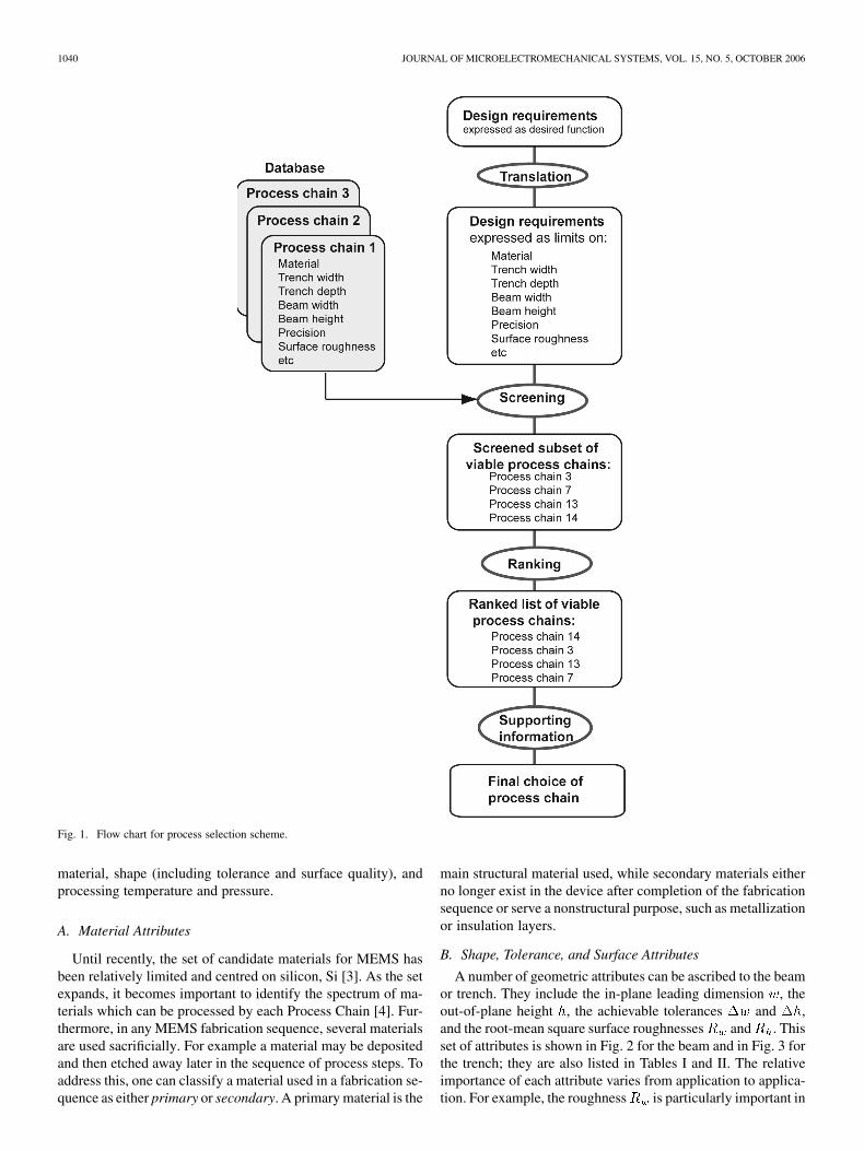
The database is used for process selection via the strategy illus-trated in Fig. 1. The performance of the planned MEMS designis translated into a set of desired feature-attributes such as ma-terial, shape, dimensions, precision etc drawn from the list usedto characterize the Process Chains. The library of Process Chainsis then screened, rejecting those incapable of making the desiredfeature from the desired material, with the desired dimensionsand precision, leaving a subset of candidates that could be usedto manufacture the MEMS device. Screening is done either man-uallyusingprocessselectionmapsordoneelectronicallyusinganappropriately constructed database and software tool, such as theCES1 Constructor and Selector system. The screened subset ofprocesses are then ranked, using approximate economic criteria,the most obvious of which is time. The final step is to search fordetailedsupporting information for the top-rankedcandidates,al-lowing an in-depth comparison of their relative merits; this stepis beyond the scope of the present study.
The outline of the paper is as follows. The process selectionmethodology is reviewed. A reduced set of geometric and ma-terial attributes is ascribed to MEMS components in the formof beams and trenches. Process selection charts are constructedfor currently available MEMS processing routes and their use isillustrated in a design example.
II. MEMS PROCESS SELECTION ATTRIBUTES
An appropriate set of Process Attributes must first be iden-tified in order to construct a library of MEMS Process Chains.The discriminating attributes for MEMS identified here include
1Granta Design Ltd., Rustat House, 62 Clifton Road, Cambridge, CB1 7EG,U.K.
1057-7157/$20.00 © 2006 IEEE
1040 JOURNAL OF MICROELECTROMECHANICAL SYSTEMS, VOL. 15, NO. 5, OCTOBER 2006
Fig. 1. Flow chart for process selection scheme.
material, shape (including tolerance and surface quality), andprocessing temperature and pressure.
A. Material Attributes
Until recently, the set of candidate materials for MEMS hasbeen relatively limited and centred on silicon, Si [3]. As the setexpands, it becomes important to identify the spectrum of ma-terials which can be processed by each Process Chain [4]. Fur-thermore, in any MEMS fabrication sequence, several materialsare used sacrificially. For example a material may be depositedand then etched away later in the sequence of process steps. Toaddress this, one can classify a material used in a fabrication se-quence as either primary or secondary. A primary material is the
main structural material used, while secondary materials eitherno longer exist in the device after completion of the fabricationsequence or serve a nonstructural purpose, such as metallizationor insulation layers.
B. Shape, Tolerance, and Surface Attributes
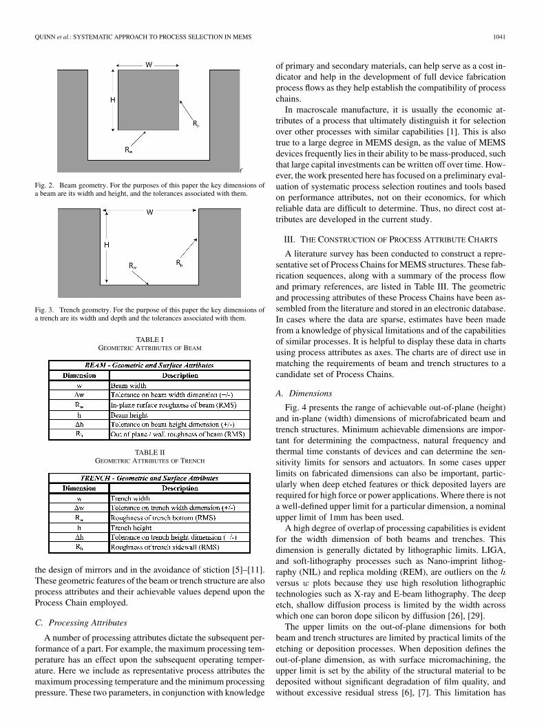
A number of geometric attributes can be ascribed to the beamor trench. They include the in-plane leading dimension , theout-of-plane height , the achievable tolerances and ,and the root-mean square surface roughnesses and . Thisset of attributes is shown in Fig. 2 for the beam and in Fig. 3 forthe trench; they are also listed in Tables I and II. The relativeimportance of each attribute varies from application to applica-tion. For example, the roughness is particularly important in
QUINN et al.: SYSTEMATIC APPROACH TO PROCESS SELECTION IN MEMS 1041
Fig. 2. Beam geometry. For the purposes of this paper the key dimensions ofa beam are its width and height, and the tolerances associated with them.
Fig. 3. Trench geometry. For the purpose of this paper the key dimensions ofa trench are its width and depth and the tolerances associated with them.
TABLE IGEOMETRIC ATTRIBUTES OF BEAM
TABLE IIGEOMETRIC ATTRIBUTES OF TRENCH
the design of mirrors and in the avoidance of stiction [5]–[11].These geometric features of the beam or trench structure are alsoprocess attributes and their achievable values depend upon theProcess Chain employed.
C. Processing Attributes
A number of processing attributes dictate the subsequent per-formance of a part. For example, the maximum processing tem-perature has an effect upon the subsequent operating temper-ature. Here we include as representative process attributes themaximum processing temperature and the minimum processingpressure. These two parameters, in conjunction with knowledge
of primary and secondary materials, can help serve as a cost in-dicator and help in the development of full device fabricationprocess flows as they help establish the compatibility of processchains.
In macroscale manufacture, it is usually the economic at-tributes of a process that ultimately distinguish it for selectionover other processes with similar capabilities [1]. This is alsotrue to a large degree in MEMS design, as the value of MEMSdevices frequently lies in their ability to be mass-produced, suchthat large capital investments can be written off over time. How-ever, the work presented here has focused on a preliminary eval-uation of systematic process selection routines and tools basedon performance attributes, not on their economics, for whichreliable data are difficult to determine. Thus, no direct cost at-tributes are developed in the current study.
III. THE CONSTRUCTION OF PROCESS ATTRIBUTE CHARTS
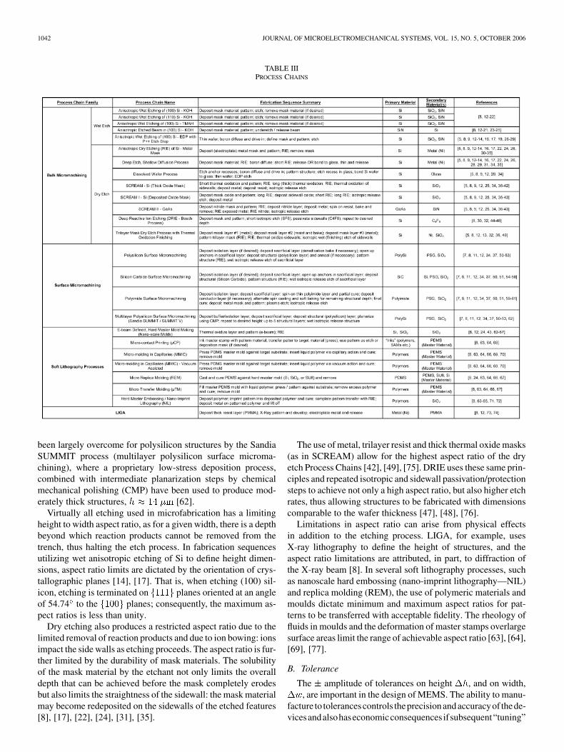
A literature survey has been conducted to construct a repre-sentative set of Process Chains for MEMS structures. These fab-rication sequences, along with a summary of the process flowand primary references, are listed in Table III. The geometricand processing attributes of these Process Chains have been as-sembled from the literature and stored in an electronic database.In cases where the data are sparse, estimates have been madefrom a knowledge of physical limitations and of the capabilitiesof similar processes. It is helpful to display these data in chartsusing process attributes as axes. The charts are of direct use inmatching the requirements of beam and trench structures to acandidate set of Process Chains.
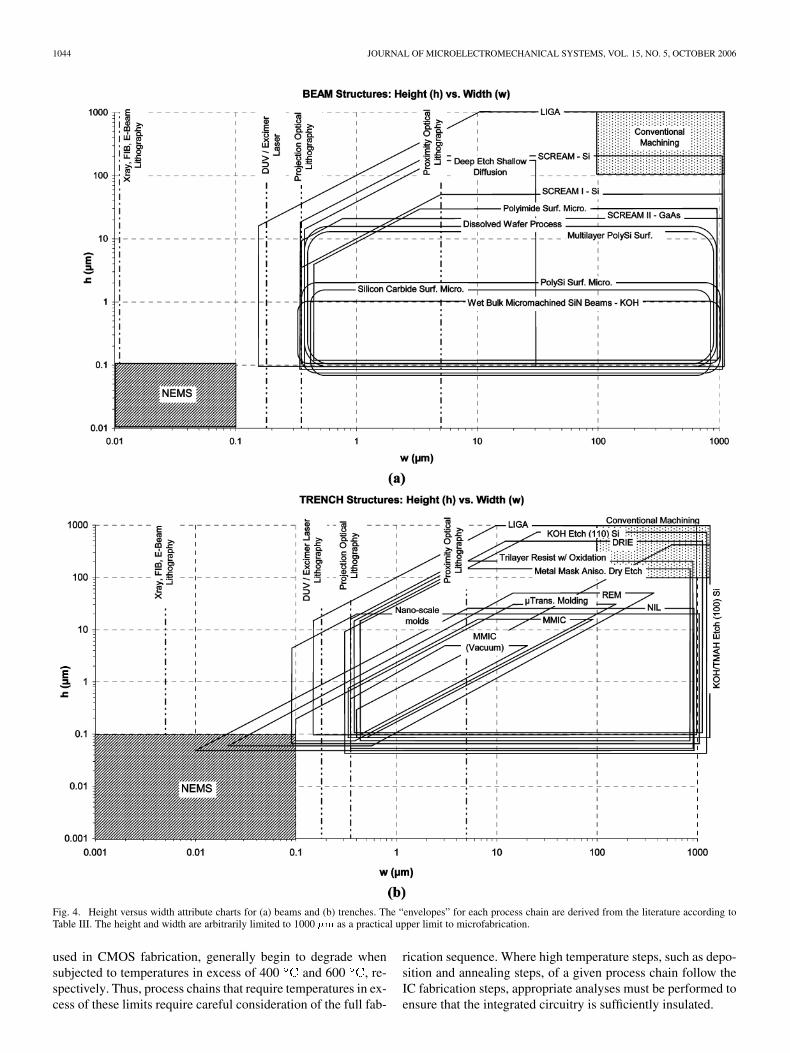
A. Dimensions
Fig. 4 presents the range of achievable out-of-plane (height)and in-plane (width) dimensions of microfabricated beam andtrench structures. Minimum achievable dimensions are impor-tant for determining the compactness, natural frequency andthermal time constants of devices and can determine the sen-sitivity limits for sensors and actuators. In some cases upperlimits on fabricated dimensions can also be important, partic-ularly when deep etched features or thick deposited layers arerequired for high force or power applications. Where there is nota well-defined upper limit for a particular dimension, a nominalupper limit of 1mm has been used.
A high degree of overlap of processing capabilities is evidentfor the width dimension of both beams and trenches. Thisdimension is generally dictated by lithographic limits. LIGA,and soft-lithography processes such as Nano-imprint lithog-raphy (NIL) and replica molding (REM), are outliers on theversus plots because they use high resolution lithographictechnologies such as X-ray and E-beam lithography. The deepetch, shallow diffusion process is limited by the width acrosswhich one can boron dope silicon by diffusion [26], [29].
The upper limits on the out-of-plane dimensions for bothbeam and trench structures are limited by practical limits of theetching or deposition processes. When deposition defines theout-of-plane dimension, as with surface micromachining, theupper limit is set by the ability of the structural material to bedeposited without significant degradation of film quality, andwithout excessive residual stress [6], [7]. This limitation has
1042 JOURNAL OF MICROELECTROMECHANICAL SYSTEMS, VOL. 15, NO. 5, OCTOBER 2006
TABLE IIIPROCESS CHAINS
been largely overcome for polysilicon structures by the SandiaSUMMIT process (multilayer polysilicon surface microma-chining), where a proprietary low-stress deposition process,combined with intermediate planarization steps by chemicalmechanical polishing (CMP) have been used to produce mod-erately thick structures, [62].
Virtually all etching used in microfabrication has a limitingheight to width aspect ratio, as for a given width, there is a depthbeyond which reaction products cannot be removed from thetrench, thus halting the etch process. In fabrication sequencesutilizing wet anisotropic etching of Si to define height dimen-sions, aspect ratio limits are dictated by the orientation of crys-tallographic planes [14], [17]. That is, when etching (100) sil-icon, etching is terminated on planes oriented at an angleof 54.74 to the planes; consequently, the maximum as-pect ratios is less than unity.
Dry etching also produces a restricted aspect ratio due to thelimited removal of reaction products and due to ion bowing: ionsimpact the side walls as etching proceeds. The aspect ratio is fur-ther limited by the durability of mask materials. The solubilityof the mask material by the etchant not only limits the overalldepth that can be achieved before the mask completely erodesbut also limits the straightness of the sidewall: the mask materialmay become redeposited on the sidewalls of the etched features[8], [17], [22], [24], [31], [35].
The use of metal, trilayer resist and thick thermal oxide masks(as in SCREAM) allow for the highest aspect ratio of the dryetch Process Chains [42], [49], [75]. DRIE uses these same prin-ciples and repeated isotropic and sidewall passivation/protectionsteps to achieve not only a high aspect ratio, but also higher etchrates, thus allowing structures to be fabricated with dimensionscomparable to the wafer thickness [47], [48], [76].
Limitations in aspect ratio can arise from physical effectsin addition to the etching process. LIGA, for example, usesX-ray lithography to define the height of structures, and theaspect ratio limitations are attributed, in part, to diffraction ofthe X-ray beam [8]. In several soft lithography processes, suchas nanoscale hard embossing (nano-imprint lithography—NIL)and replica molding (REM), the use of polymeric materials andmoulds dictate minimum and maximum aspect ratios for pat-terns to be transferred with acceptable fidelity. The rheology offluids in moulds and the deformation of master stamps overlargesurface areas limit the range of achievable aspect ratio [63], [64],[69], [77].
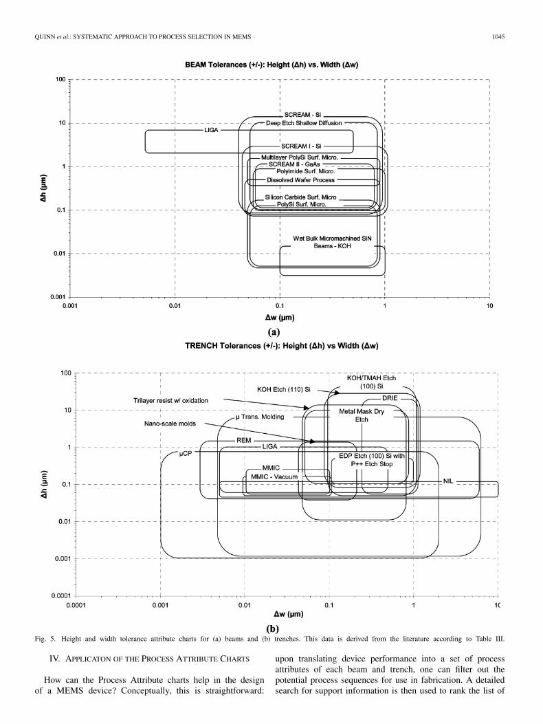
B. Tolerance
The amplitude of tolerances on height , and on width,, are important in the design of MEMS. The ability to manu-
facture to tolerancescontrols theprecisionandaccuracyof thede-vicesandalsohaseconomicconsequences ifsubsequent“tuning”

QUINN et al.: SYSTEMATIC APPROACH TO PROCESS SELECTION IN MEMS 1043
or rework steps are required to compensate for poor tolerances.Tolerances, expressed as absolute dimensions, are plotted in thetolerance maps of Fig. 4 for the library of Process Chains.
Typically, the lithographic step dictates the width tolerance.This is reflected in the Process Chains using high-resolutionlithographic steps such as LIGA and various soft-lithographyprocesses. In addition to lithography, one must consider the sub-sequent etch steps of the fabrication sequence. If the etch givessignificant mask undercutting, the tolerance on the width di-mension increases. This is reflected by the relative width tol-erance for anisotropic wet and dry etch based processes: theoccurrence of mask misalignment and crystallographic etchingin wet etch based processes leads to a greater width tolerancethan anisotropic dry etch based processes, assuming the use ofdurable mask materials in the dry etch process [8], [14], [17].Similarly, in DRIE, isotropic dry etching gives mask undercut-ting and a consequent increase in width tolerance [35].
Several soft lithography processes involve the casting andcuring of polymers in a moulding or stamping process. The re-sulting shrinkage and expansion by 1–3% contribute to the tol-erances that can be held in the in-plane dimensions [63], [64],[77]–[79].
Tolerances in the height dimension are generally dictatedby the etching or deposition processes used in the fabricationsequence. Where deposition steps define the height of a struc-ture, as in surface micromachining, the out-of-plane dimensioncan be controlled down to nanometer level. Poorer tolerancesare achieved by multilayer surface micromachining where thetolerance on the out-of-plane dimension is cumulative overmultiple deposition steps, and by polyimide surface microma-chining where the use of spin casting is less accurate than otherdeposition techniques [59], [60].
Next, consider a structure of height dictated by a single etchstep. Structures whose height is defined by a single etch stepgenerally have tighter tolerances using dry etching than wetetching. In standard anisotropic wet etch processes, even if onehas accurate control over the concentration, stirring and reac-tant removal, it is difficult to control the depth of etch to betterthan 10% of the nominal depth [17]. This is unacceptable whenmaking structures requiring depths of etch in excess of a coupleof hundred microns, such as in the fabrication of thin mem-branes, where control of the thickness of the membrane is crit-ical. Tighter tolerances on depth dimensions can be attained byanisotropic dry etching due to close control over the pressure,bias, gas flow and other process variables [22].
The use of an etch stop in wet bulk micromachining allowsfor a tight tolerance on the depth dimension, see Fig. 5. For ex-ample, a diffused and driven-in boron layer (p++ doped) can beused to define the depth of etch. This diffusion layer is largely re-sistant to EDP etching, allowing for depth control in the submi-cron domain [8], [28]. Other etch stop procedures, such as elec-trochemical and material stops, particularly buried oxide layersin silicon on insulator wafers, have a similar performance [17],[27].
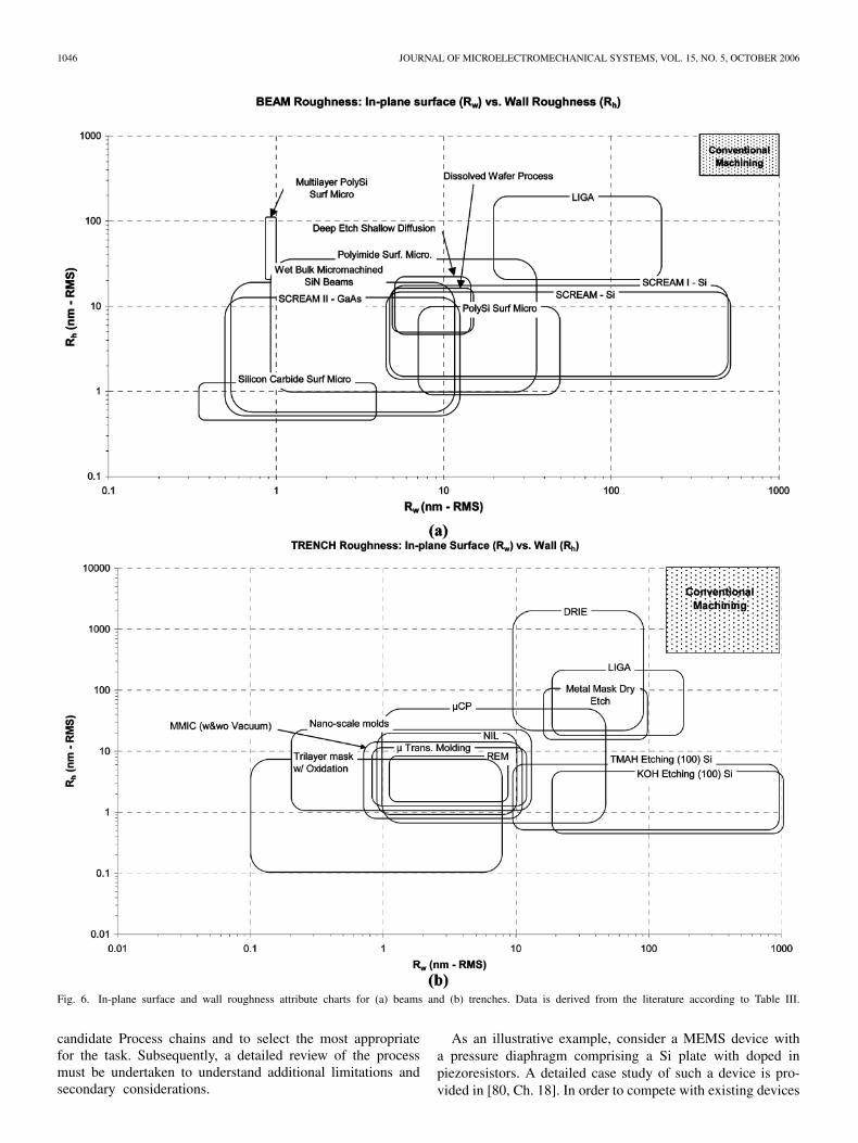
C. Roughness
Fig. 6 presents Process Attribute maps for in-planesurface roughness and side-wall roughness, given as the
root-mean-square (rms) values. Roughness is important foroptical applications where reflectivity is required. High rough-ness is undesirable in tribological applications, but may bedesirable if stiction is to be avoided. Roughness also plays arole in dictating the strength of the resulting structure. Again,the roughness characteristics are dictated mainly by the combi-nation of etching and deposition used in each Process Chain.
Dry etch processes have the potential for attaining very lowsurface roughness both in-plane and in the side-wall direction.An exception is DRIE, where the alternating etch and passiva-tion steps creates a scalloping of the sidewalls and roughnessup to the micron level [47], [48]. In anisotropic wet etching, theside-walls can be aligned with crystallographic planes and theresulting roughness can be of atomic magnitude. Wet etchingalso has the potential to leave extremely rough in-plane surfaces:the roughness of planes exceeds that of planes[15]. Improved surface roughnesses are achieved in doped sil-icon through the use of an etch stop or a deep etch shallow dif-fusion sequence.
The use of finishing steps to improve surface and side-wallroughness in Process Chains is included in Fig. 6. In-planeroughness can be improved dramatically by the use of CMPsteps, as illustrated by multilayer surface micromachining. An-other common technique for reducing both in-plane and sidewallroughness, shown here in combination with a trilayer resist maskdry etch process, is the use of an oxidation finishing step, wherethermal oxidation followed by a wet etch dramatically reducesthe roughness of the as-etched or oxidized surface [5], [19].
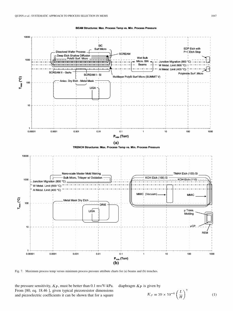
D. Pressure and Temperature
Fig. 7 presents a chart of the maximum process temperatureversus minimum processing pressure for the MEMS ProcessChains. These two parameters are important for several reasons.First, they are often indicative of the cost and time of a ProcessChain, such as the capital cost of high temperature or vacuumequipment, and the time necessary to carry out high tempera-ture or high vacuum steps. Second, these attributes allow thedesigner to discriminate between those candidate process chainsthat can be carried out “in-house” and those that must be out-sourced for fabrication. This is an indirect cost indicator. Andthird, these parameters determine the compatibility of differentProcess Chains and materials. That is, if one wanted to fabricatea complete device using a series of Process Chains, compati-bility can only be assured if the maximum temperature of theProcess Chain considered does not exceed the melting temper-ature of the materials present in an early fabrication sequence.Similarly, one could not use a high vacuum fabrication sequencefollowing a fabrication sequence that leaves potentially contam-inating materials.
The maximum process temperature and minimum processingpressure also dictate whether these process sequences can becarried out on IC circuitry. The integration of mechanical andelectronic subsystems is part of the more general issue of pack-aging, an important issue which must be addressed at the ear-liest stages of design [80]. Junction migration will occur at ap-proximately 800 for shallow junctions. Thus, temperaturesin excess of this limit should be avoided for integration with ICcircuitry. In addition, aluminium and tungsten, common metals
1044 JOURNAL OF MICROELECTROMECHANICAL SYSTEMS, VOL. 15, NO. 5, OCTOBER 2006
Fig. 4. Height versus width attribute charts for (a) beams and (b) trenches. The “envelopes” for each process chain are derived from the literature according toTable III. The height and width are arbitrarily limited to 1000 �m as a practical upper limit to microfabrication.
used in CMOS fabrication, generally begin to degrade whensubjected to temperatures in excess of 400 and 600 , re-spectively. Thus, process chains that require temperatures in ex-cess of these limits require careful consideration of the full fab-
rication sequence. Where high temperature steps, such as depo-sition and annealing steps, of a given process chain follow theIC fabrication steps, appropriate analyses must be performed toensure that the integrated circuitry is sufficiently insulated.
QUINN et al.: SYSTEMATIC APPROACH TO PROCESS SELECTION IN MEMS 1045
Fig. 5. Height and width tolerance attribute charts for (a) beams and (b) trenches. This data is derived from the literature according to Table III.
IV. APPLICATON OF THE PROCESS ATTRIBUTE CHARTS
How can the Process Attribute charts help in the designof a MEMS device? Conceptually, this is straightforward:
upon translating device performance into a set of processattributes of each beam and trench, one can filter out thepotential process sequences for use in fabrication. A detailedsearch for support information is then used to rank the list of
1046 JOURNAL OF MICROELECTROMECHANICAL SYSTEMS, VOL. 15, NO. 5, OCTOBER 2006
Fig. 6. In-plane surface and wall roughness attribute charts for (a) beams and (b) trenches. Data is derived from the literature according to Table III.
candidate Process chains and to select the most appropriatefor the task. Subsequently, a detailed review of the processmust be undertaken to understand additional limitations andsecondary considerations.
As an illustrative example, consider a MEMS device witha pressure diaphragm comprising a Si plate with doped inpiezoresistors. A detailed case study of such a device is pro-vided in [80, Ch. 18]. In order to compete with existing devices
QUINN et al.: SYSTEMATIC APPROACH TO PROCESS SELECTION IN MEMS 1047
Fig. 7. Maximum process temp versus minimum process pressure attribute charts for (a) beams and (b) trenches.
the pressure sensitivity, , must be better than 0.1 mv/V-kPa.From [80, eq. 18.46 ], given typical piezoresistor dimensionsand piezoelectric coefficients it can be shown that for a square
diaphragm is given by
(1)

1048 JOURNAL OF MICROELECTROMECHANICAL SYSTEMS, VOL. 15, NO. 5, OCTOBER 2006
where is in units of mv/V-kPa, and where and are thein-plane dimension (width) and thickness of the diaphragm re-spectively. Thus to achieve the required sensitivity, mustexceed 50. Since the diaphragm is essentially a beam struc-ture, this design constraint can be plotted on Fig. 4(a). It cre-ates a triangular area in the bottom right-hand corner of mostof the process lozenges. By this metric most of the bulk micro-machining processes appear as candidates, capable of creatingmembranes with dimensions of 1000 by 20 thick downto 10 by 0.2 thick.
A second important consideration is the accuracy of thesensor. Currently piezoresistive pressure sensors require elec-trical calibration using laser trimming of the resistors. Onecontribution to this is the tolerances on the microfabrication ofthe diaphragm. An accuracy of better than 1% is required forautomotive applications (see [80, Table 17.1, Ch. 17]). If thisstep could be avoided, by choice of a suitable process chain,then it would have considerable impact on the cost of fabri-cation of such sensors. Consider a large diaphragm, 1000by 20 thick. In the absence of any thickness variation, awidth variation of 5 is permissible according to (1).This is clearly achieved, see Fig. 5(a). However, in the absenceof any width variation, a thickness tolerance of 0.1 must beheld. From Fig. 5(a), this is marginal for bulk micromachiningprocesses, and given other sources of error, it is clear thatmicrofabrication alone cannot be relied upon to achieve therequired accuracy. Greater inaccuracies are anticipated forsmaller pressure sensors in their as-processed state. We alsonote in passing that temperature compensation and packagingintroduced stresses are additional drivers for the laser trimmingstep.
Pursuing the pressure sensor example further, accepting theneed to use laser trimming to compensate for the limits inmanufacturing tolerances, if the device is to have embeddedIC circuitry with aluminium metallization, this requires theprocessing temperature not to exceed 400 , On referring toFig. 7(a), this would eliminate some process chains involvingbonding or doping. From Figs. 5(a) and 7(a) it can be seen thatthe principal candidate process chains are: DRIE, AnisotropicKOH etching or TMAH etching of (110) Si. In all cases thediaphragm would be formed by etching down from the backsideof the wafer, either as a timed etch, or to an etch stop. Additionalconsiderations of cost and process sequence compatibility areneeded to identify the best choice. It is clear from this examplethat a systematic consideration of the functional requirementshelps to narrow the process selection substantially.
V. CONCLUDING REMARKS
The most obvious limitation of the work presented here isthat due to the accuracy and availability of processing data.Typically, the focus of much of the literature on fabrication se-quences is neither on process control nor on absolute limits ofthe Process Chains but on particular devices fabricated usingthese Process Chains. Few, if any, statistical measures are givento indicate the distribution of the data. Nevertheless, for the pur-poses of evaluating the use of a systematic approach to MEMSprocess selection and its associated tools, the data presented here
are considered to be adequate. An additional limitation is thelack of economic and time data presented here; this is the sub-ject of future work.
A systematic approach to process selection in MEMS hasbeen presented. Process Attribute maps have been constructedand used to quantify the relative merit of existing Process Chainsfor MEMS fabrication. In discussing the construction of thesemaps the process steps of lithography, deposition and etchinghave been highlighted as controlling the overall performance ofMEMS fabrication sequences. The Process Attribute maps haveadditional value as educational tools and in motivating the fur-ther development of MEMS fabrication techniques to extend thecoverage of processing space.
REFERENCES
[1] M. F. Ashby, Materials Selection in Mechanical Design. Boston,MA: Butterworth Heinemann, 1999.
[2] A. M. K. Esawi and M. F. Ashby, Computer-Based Selection of Man-ufacturing Processes Cambridge Univ. Eng. Dept., Cambridge, 1997,CUED Report TR50.
[3] S. M. Spearing, Materials Issues in Microelectromechanical Systems(MEMS). New York: Acta Materiala, 2000, vol. 48, pp. 179–196.
[4] V. T. Srikar and S. M. Spearing, “Materials selection in microme-chanical design: An application of the Ashby approach,” J. Microelec-tromech. Syst., vol. 12, pp. 3–10, 2003.
[5] W. H. Juan and S. W. Pang, “Controlling sidewall smoothness for mi-cromachined Si mirrors and lenses,” J. Vacuum Sci. Technol. B, vol. 14,pp. 4080–4084, 1996.
[6] R. T. Howe, “Surface micromachining for microsensors and microac-tuators,” J. Vacuum Sci. Technol. B, vol. 6, pp. 1809–1813, 1988.
[7] J. Bustillo, R. Howe, and R. Muller, “Surface micromachining for mi-croelectromechanical systems,” Proc. IEEE, vol. 86, pp. 1552–1574,1998.
[8] M. Madou, Fundamentals of Microfabrication, 2 ed. Boca Raton, FL:CRC Press, 2002.
[9] W. H. Juan and S. W. Pang, “High-Aspect-Ratio Si vertical mi-cromirror arrays for optical switching,” J. Microelectromech. Syst.,vol. 7, pp. 207–213, 1998.
[10] H. Toshiyoshi and H. Fujita, “Electrostatic micro torsion mirrors for anoptical switch matrix,” J. Microelectromech. Syst., vol. 5, pp. 231–237,1996.
[11] J. Zou, M. Balberg, C. Byrne, C. Liu, and D. Brady, “Optical proper-ties of surface micromachined mirrors with etch holes,” J. Microelec-tromech. Syst., vol. 8, pp. 506–513, 1999.
[12] The MEMS Exchange [Online]. Available: http://www.mems-ex-change.net
[13] G. Kaminsky, “Micromachining of silicon mechanical structures,” J.Vacuum Sci. Technol. B, vol. 3, pp. 1015–1024, 1985.
[14] G. Kovacs, N. I. Maluf, and K. Petersen, “Bulk micromachining ofsilicon,” Proc. IEEE, vol. 86, pp. 1536–1551, 1998.
[15] E. D. Palik, O. J. Glmbocki, I. Heard, P. S. Burno, and L. Tenerz,“Etching roughness for (100) silicon surfaces in Aqueous KOH,” J.Appl. Phys., vol. 70, pp. 3291–3300, 1991.
[16] N. I. Maluf, An Introduction to Microelectromechanical Systems(MEMS). Boston, MA: Artech House, 2000.
[17] M. Elwenspoek and H. V. Jansen, Silicon Micromachining. Cam-bridge, U.K.: Cambridge University Press, 1998.
[18] P. Krause and E. Obermeier, “Etch rate and surface roughness of deepnarrow U- grooves in (110)-oriented silicon,” J. Micromech. Microeng.,vol. 5, pp. 112–114, 1995.
[19] K. Lee, D. Lim, and L. Kimerling, “Fabrication of ultralow-lossSi/SiO waveguides by roughness reduction,” Opt. Lett., vol. 26, pp.1888–1890, 2001.
[20] D. Resnik, D. Vrtacnik, U. Aljancic, and S. Amon, “Effective rough-ness reduction of f100g and f311g planes in anisotropic etching off100g silicon in 5% TMAH,” J. Micromech. Microeng., vol. 13, pp.26–34, 2003.
[21] M. Lambrechts and W. Sansen, Biosensors: Microelectrical De-vices. Philadelphia, PA: Institute of Physics Publishers, 1992.
[22] D. Manos and D. Flamm, Plasma Etching—An Introduction. Boston,MA: Academic, 1989.
QUINN et al.: SYSTEMATIC APPROACH TO PROCESS SELECTION IN MEMS 1049
[23] Y. B. Park and S. W. Rhee, “Bulk and interface properties of low-temperature silicon nitride films deposited by remote plasma enhancedchemical vapor deposition,” J. Mater. Sci.: Mater. Electron., vol. 12,pp. 515–522, 2001.
[24] R. G. Poulsen, “Plasma etching in integrated circuit manufacture—Areview,” J. Vacuum Sci. Technol. B, vol. 14, pp. 266–274, 1977.
[25] C. Reyes-Betanzo, S. A. Moshkalyov, M. A. Cotta, M. A. Pavanello, A.C. S. Ramos, and J. W. Swart, “Plasma etching of silicon nitride withhigh selectivity over silicon oxide and silicon in fluorine containingplasmas,” J. Vacuum Sci. Technol. A, vol. 17, pp. 3179–3179, 1999.
[26] W. H. Juan and S. W. Pang, “Released Si microstructures fabricated bydeep etching and shallow diffusion,” J. Microelectromech. Syst., vol. 5,pp. 18–23, 1996.
[27] B. Kloeck, S. Collins, N. D. Rooij, and R. Smith, “Study of electro-chemical etch-stop for high-precision thickness control of silicon mem-branes,” IEEE Trans. Electron Devices, vol. 36, pp. 663–669, 1989.
[28] C. Huang and K. Najafi, “Fabrication of ultrathin p++ siliconmicrostructures using ion implantation and boron etch-stop,” J. Mi-croelectromech. Syst., vol. 10, pp. 532–537, 2001.
[29] J. W. Weigold and S. W. Pang, “Fabrication of thick Si resonators witha frontside-release etch-diffusion process,” J. Microelectromech. Syst.,vol. 7, pp. 201–206, 1998.
[30] J. Bhardwaj, H. Ashraf, and A. McQuarrie, “Dry silicon etching forMEMS,” in Proc. Annu. Meeting Electrochem. Soc., Montreal, QC,Canada, 1997.
[31] H. Jansen, H. Gardeniers, M. d. Boer, M. Elwenspoek, and J. Fluitman,“A survey on the reactive ion etching of silicon in microtechnology,”J. Micromech. Microeng., vol. 6, pp. 14–28, 1996.
[32] C. Zhao, Y. Z. Hu, T. Labayen, L. Lai, and E. A. Irene, “Comparison ofSi/SiO interface roughness from electron cyclotron resonance plasmaand thermal oxidation,” J. Vacuum Sci. Technol. A, vol. 16, pp. 57–62,1998.
[33] M. R. Rakhshandehroo, J. W. Weigold, W. C. Tian, and S. W. Pang,“Dry etching of Si field emitters and high aspect ratio resonators usingan inductively coupled plasma source,” J. Vacuum Sci. Technol. B, vol.16, pp. 2849–2854, 1998.
[34] W. H. Juan and S. W. Pang, “Control of etch profile for fabrication ofSi microsensors,” J. Vacuum Sci. Technol. A, vol. 14, pp. 1189–1193,1996.
[35] W. C. Tian, J. W. Weigold, and S. W. Pang, “Comparison of Cl2 andF-based dry etching for high aspect raio Si microstructures etched withan inductively coupled plasma source,” J. Vacuum Sci. Technol. B, vol.18, pp. 1890–1896, 2000.
[36] Z. L. Zhang and N. MacDonald, “Fabrication of submicron high-as-pect-ratio GaAs actuators,” J. Microelectromech. Syst., vol. 2, pp.66–73, 1993.
[37] Handbook of Micro/Nano Tribology2 ed. Boca Raton, FL, CRCPress, 1995.
[38] Dry Etching of Silicon Obermeier. MAT, Berlin [Online]. Available:http://www-mat.ee.tu-berlin.de/research/dryetch/dryetch.htm
[39] R. Petri, P. Brault, O. Vatel, D. Henry, E. Andre, P. Dumas, and F.Salvan, “Silicon roughness induced by plasma etching,” J. Appl. Phys.,vol. 75, pp. 7498–7506, 1994.
[40] N. C. MacDonald, MicroElectomechanical Systems Module: SingleCrystal Reactive Etching and Metallization (SCREAM) Process[Online]. Available: http://designstudio.mae.cornell.edu/realiza-tion/mems-module
[41] Z. L. Zhang and N. MacDonald, “A rie process for submicron, sil-icon electromechanical structures,” J. Micromech. Microeng., vol. 2,pp. 31–38, 1992.
[42] N. C. MacDonald, “SCREAM microelectromechanical systems,” Mi-croelectron. Eng., vol. 32, pp. 49–73, 1996.
[43] Microelectronics Fabrication Facility Hong Kong Institute of Scienceand Technology [Online]. Available: http://www.mff.ust.hk
[44] High Aspect Ratio Etching Protron Mikrotechnik [Online].Available: http://www.protron-mikrotechnik.de/technology/tech-nology_ase_e_2.htm
[45] L. Chen, H. Neves, and T. Kudrle, Cornell Nanofabrication Facility:National Nanofabrication Users Network. Process Development for theIntegration of MEMS and RF Devices [Online]. Available: http://www.nnf.cornell.edu/1999REU/ra/Chen.pdf
[46] W. C. Tian and S. W. Pang, “Freestanding microheaters in Si with highaspect ratio microstructures,” J. Vacuum Sci. Technol. B, vol. 20, pp.1008–1012, 2002.
[47] A. A. Ayon, R. A. Braff, R. Bayt, H. H. Sawin, and M. A. Schmidt,“Characterization of a time multiplexed inductively coupled plasmaetcher,” J. Electrochem. Soc., vol. 146, pp. 339–349, 1999.
[48] ——, “Influence of coil power on the etching characteristics in a highdensity plasma etcher,” J. Electrochem. Soc., vol. 146, pp. 2730–2736,1999.
[49] F. Eberhard and E. Deichsel, Fabrication of Vertical Facets in AlGaAsUsing Chemically-Assisted Ion-Beam Etching Univ. of Ulm, Dept.Optoelectronics, 1997, Annual Report.
[50] PHS MEMS [Online]. Available: www.phsmems.com[51] P. Chabert, “Deep etching of silicon carbide for micromachining ap-
plications: Etch rates and etch mechanisms,” J. Vacuum Sci. Technol.B, vol. 19, pp. 1339–1345, 2001.
[52] G. F. Cardinale, C. C. Henderson, J. E. M. Goldsmith, P. J. S. Mangat,J. Cobb, and S. D. Hector, “Demonstration of pattern transfer into sub-100nm polysilicon line/space features patterned with extreme ultravi-olet lithography,” J. Vacuum Sci. Technol. A, vol. 17, pp. 2970–2974,1999.
[53] R. Hegde, W. Paulson, and P. Tobin, “Surface topography of phos-phorous doped polysilicon,” J. Vacuum Sci. Technol. B, vol. 13, pp.1434–1441, 1995.
[54] B. Kim, H. Choi, and B. Lee, “Surface roughness of silicon carbideetched in a C F =O inductively coupled plasma,” J. Vacuum Sci.Technol. A, vol. 20, pp. 424–429, 2002.
[55] A. R. Shrimkunas, P. E. Mauger, L. P. Bourget, R. S. Post, L. Smith,R. F. Davis, G. M. Wells, F. Cerrina, and R. B. McIntosh, “Advancedelectron cylcotron resonance chemical vapor deposition sic coatingsand x-ray mask membranes,” J. Vacuum Sci. Technol. B, vol. 9, pp.3258–3261, 1991.
[56] N. Agarwal, S. Ponoth, J. Plawsky, and P. Persans, “Optimized oxygenplasma etching of polyimide films for low loss optical waveguides,” J.Vacuum Sci. Technol. A, vol. 20, pp. 1587–1591, 2002.
[57] P. Neudeck, Recent Progress in Silicon Carbide Semiconductor Elec-tronics Technology NASA Glenn Research Center, 2001 [Online].Available: http://www.grc.nasa.gov/www/SiC/SiCReview.html
[58] SiC MEMS at CWRU Case Western Reserve University [Online].Available: http://mems.cwru.edu/SiC
[59] M. A. Schmidt, R. T. Howe, S. Senturia, and J. Haritonidis, “Designand calibration of a microfabricated floating-element shear-stresssensor,” IEEE Trans. Electron Devices, vol. 35, pp. 750–757, 1988.
[60] S. Bagen, Photoresist Coating Methods MEMS Exchange, 1997 [On-line]. Available: http://mail.mems-exchange.org/pipermail/mems-talk/1997-September/001056.html
[61] K. Suzuki and I. Shimoyama, “Insect-Model based microrobot withelastic hinges,” J. Microelectromech. Syst., vol. 3, pp. 4–9, 1994.
[62] SUMMIT V Sandia National Laboratories [Online]. Available: http://www.sandia.gov
[63] Y. Xia and G. Whitesides, Soft Lithography. : AngewandteChemie—International Edition, 1998, vol. 37, pp. 550–575.
[64] ——, “Soft lithography,” Annu. Rev. Mater. Sci., vol. 28, pp. 153–184,1998.
[65] S. Chou, P. Krauss, and P. Renstrom, “Imprint lithography with25-nanometer resolution,” Science, vol. 272, pp. 85–87, 1996.
[66] B. D. Terris, H. J. Mamin, M. E. Best, J. A. Logan, D. Rugar, and S.A. Rishton, “Nanoscale replication for scanning probe data storage,”Appl. Phys. Lett., vol. 69, pp. 4262–4264, 1996.
[67] Y. Z. Hu, P. P. Buaud, L. Spanos, Y. Q. Wang, M. Li, and E. A. Irene,“In situ electron cyclotron resonance plasma surface cleaning of sil-icon,” J. Vacuum Sci. Technol. A, vol. 12, pp. 1315–1321, 1994.
[68] M. J. Lercel, C. S. Whelan, H. G. Craighead, K. Seshadri, and D. L.Allara, “High-Resolution silicon patterning with self-assembled mono-layer resists,” J. Vacuum Sci. Technol. B, vol. 14, pp. 4085–4090, 1996.
[69] N. L. Jeon, I. S. Choi, B. Zu, and G. Whitesides, “Large area patterningby vacuum-assisted micromolding,” Adv. Mater., vol. 11, pp. 946–950,1999.
[70] J. Rogers, Z. Bao, and V. R. Raju, “Nonphotolithographic fabricationof organic transistors with micron feature sizes,” Appl. Phys. Lett., vol.72, pp. 2716–2718, 1998.
[71] P. Krauss and S. Y. Chou, “Nano-compact disks with 400 Gbit=in̂2storage density fabricated using nanoimprint lithography and read withproximal probe,” Appl. Phys. Lett., vol. 71, pp. 3174–3176, 1997.
[72] S. Chou, P. Krauss, and P. Renstrom, “Imprint of sub-25 nmvias and trenches in polymers,” Appl. Phys. Lett., vol. 67, pp.3114–3116, 1995.
[73] A. B. Frazier and M. G. Allen, “Metallic microstructures fabricatedusing photosensitive polyimide electroplating molds,” J. Microelec-tromech. Syst., vol. 2, pp. 87–94, 1993.
[74] A. Rogner, J. Eicher, D. Munchmeyer, R. Peters, and J. Mohr, “The ligatechnique—What are the new opportunities,” J. Micromech. Microeng.,vol. 2, pp. 133–140, 1992.
1050 JOURNAL OF MICROELECTROMECHANICAL SYSTEMS, VOL. 15, NO. 5, OCTOBER 2006
[75] A. Mehra, X. Zhang, A. Ayon, I. Waitz, M. Schmidt, and C. Spadac-cini, “A six-wafer combustion system for a silicon micro gas turbineengine,” J. Microelectromech. Syst., vol. 9, pp. 517–527, 2000.
[76] K. Ishihara, C. Yung, A. Ayon, and M. Schmidt, “An intertial sensortechnology using drie and wafer bonding with interonnecting capa-bility,” J. Microelectromech. Syst., vol. 8, pp. 403–408, 1999.
[77] J. Rogers, K. Paul, and G. Whitesides, “Quantifying distortions in softlithography,” J. Vacuum Sci. Technol. B, vol. 16, pp. 88–97, 1997.
[78] Y. Xia, E. Kim, X. Zhao, J. Rogers, M. Prentiss, and G. Whitesides,“Complex optical surfaces formed by replica molding against eleast-omeric masters,” Science, vol. 273, pp. 347–349, 1996.
[79] Y. Xia, J. Rogers, K. Paul, and G. Whitesides, “Unconventionalmethods for fabricating and patterning nanostructures,” Chem. Rev.,vol. 99, pp. 1823–1848, 1999.
[80] S. Senturia, Microsystem Design. Boston, MA: Kluwer Academic,2002.
David J. Quinn is currently working towards thePh.D. degree at the Massachusetts Institute ofTechnology (MIT), Cambridge, where he receivedthe M.Sc. degree in mechanical engineering in 2006.Prior to attending MIT, he received the M.Phil.degree in engineering by research from CambridgeUniversity, Cambridge, U.K., in 2003 and the B.Sc.degree in mechanical engineering at VillanovaUniversity, Villanova, PA.
His technical interests include mechanical be-havior of materials and structural design and analysis
of MEMS. He has been awarded the Fulbright and Gates Cambridge Scholar-ships as well as the National Defense Science and Engineering and NationalScience Foundation Graduate Research Fellowships.
Mr. Quinn is a member of the American Society of Mechanical Engineers(ASME).
S. Mark Spearing received the Ph.D. degree fromCambridge University Engineering Department,U.K., in 1990.
In 2004, he was appointed Professor of Engi-neering Materials in the School of EngineeringSciences at The University of Southampton, U.K.Prior to this, he spent 10 years as Professor ofAeronautics and Astronautics at the MassachusettsInstitute of Technology (MIT), Cambridge. Histechnical interests include materials characterizationand structural analysis and design of MEMS, devel-
opment of wafer bonding-technologies, microelectronic and MEMS packaging,and advanced composites. From 1995 to 2005, he was responsible for materials,structural design, and packaging tasks of the MIT MicroEngine, MicroRocket,Micro-Chemical Power, and MicroHydraulic Transducer projects as well asconducting cross-cutting underpinning technology development.
Dr. Spearing is an Associate Editor of the JOURNAL OF
MICROELECTROMECHANICAL SYSTEMS and Member of the AmericanSociety of Mechanical Engineers (ASME). In 2004, he received a RoyalSociety Wolfson Research Merit Award.
Mike Ashby is a Royal Society Research Professorat the University of Cambridge, U.K., and a RoyalAcademy of Engineering Visiting Professor at theRoyal College of Art in London. He is the author ofa number of books on materials. Among the morerecent are Engineering Materials, Volumes 1 and 2(3rd edition 2005), Cellular Solids (1988, 2nd edition1997), Materials Selection in Mechanical Design(1992, 3rd edition 2005), “Metal Foams—A DesignGuide (2000), and Materials and Design—the Artand Science of Materials Selection in Product
Design (2002). His interests are in design, and in the role materials play in it.
Norman A. Fleck is Head of Mechanics, Materialsand Design at Cambridge University, EngineeringDepartment. He did his undergraduate and graduatework at the University of Cambridge, and wasa Postdoctoral Researcher at Harvard Universitybefore returning to the staff at Cambridge Univer-sity. His research interests are in the mechanics ofmaterials, and is currently researching the mechanicsof MEMS, lattice materials, thermal barrier coatings,and skin.

![JOURNAL OF MICROELECTROMECHANICAL SYSTEMS, VOL…nelsons/Papers/Merced et al JMEMS 2014.pdf · JOURNAL OF MICROELECTROMECHANICAL SYSTEMS, VOL. 23, NO. 5, ... [2], [3] to mechanical](https://img.dokumen.tips/doc/110x75/5b2d83807f8b9ab66e8bec7e/journal-of-microelectromechanical-systems-nelsonspapersmerced-et-al-jmems-2014pdf.jpg)