Embed Size (px)
Citation preview
1/25October 2005
M24C16, M24C08M24C04, M24C02, M24C01
16Kbit, 8Kbit, 4Kbit, 2Kbit and 1Kbit Serial I²C Bus EEPROM
FEATURES SUMMARY Two-Wire I²C Serial Interface
Supports 400kHz Protocol Single Supply Voltage:
– 2.5 to 5.5V for M24Cxx-W– 1.8 to 5.5V for M24Cxx-R
Write Control Input BYTE and PAGE WRITE (up to 16 Bytes) RANDOM and SEQUENTIAL READ Modes Self-Timed Programming Cycle Automatic Address Incrementing Enhanced ESD/Latch-Up Protection More than 1 Million Erase/Write Cycles More than 40-Year Data Retention Packages
– ECOPACK® (RoHS compliant)
Table 1. Product List
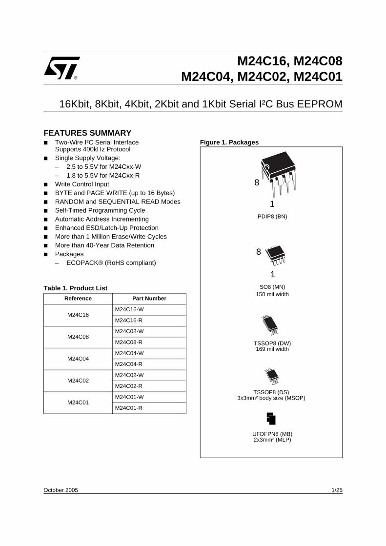
Figure 1. Packages
Reference Part Number
M24C16M24C16-W
M24C16-R
M24C08M24C08-W
M24C08-R
M24C04M24C04-W
M24C04-R
M24C02M24C02-W
M24C02-R
M24C01M24C01-W
M24C01-R
PDIP8 (BN)
SO8 (MN)150 mil width
8
1
TSSOP8 (DW)169 mil width
TSSOP8 (DS)3x3mm² body size (MSOP)
8
1
UFDFPN8 (MB)2x3mm² (MLP)
M24C16, M24C08, M24C04, M24C02, M24C01
2/25
TABLE OF CONTENTS
FEATURES SUMMARY . . . . . . . . . . . . . . . . . . . . . . . . . . . . . . . . . . . . . . . . . . . . . . . . . . . . . . . . . . . . . 1
SUMMARY DESCRIPTION. . . . . . . . . . . . . . . . . . . . . . . . . . . . . . . . . . . . . . . . . . . . . . . . . . . . . . . . . . . 3
Device internal reset . . . . . . . . . . . . . . . . . . . . . . . . . . . . . . . . . . . . . . . . . . . . . . . . . . . . . . . . . . . . 3
SIGNAL DESCRIPTION . . . . . . . . . . . . . . . . . . . . . . . . . . . . . . . . . . . . . . . . . . . . . . . . . . . . . . . . . . . . . 4
Serial Clock (SCL) . . . . . . . . . . . . . . . . . . . . . . . . . . . . . . . . . . . . . . . . . . . . . . . . . . . . . . . . . . . . . . . 4Serial Data (SDA) . . . . . . . . . . . . . . . . . . . . . . . . . . . . . . . . . . . . . . . . . . . . . . . . . . . . . . . . . . . . . . . 4Chip Enable (E0, E1, E2) . . . . . . . . . . . . . . . . . . . . . . . . . . . . . . . . . . . . . . . . . . . . . . . . . . . . . . . . . 4Write Control (WC) . . . . . . . . . . . . . . . . . . . . . . . . . . . . . . . . . . . . . . . . . . . . . . . . . . . . . . . . . . . . . . 4
DEVICE OPERATION . . . . . . . . . . . . . . . . . . . . . . . . . . . . . . . . . . . . . . . . . . . . . . . . . . . . . . . . . . . . . . . 6
Start Condition. . . . . . . . . . . . . . . . . . . . . . . . . . . . . . . . . . . . . . . . . . . . . . . . . . . . . . . . . . . . . . . . . 6Stop Condition. . . . . . . . . . . . . . . . . . . . . . . . . . . . . . . . . . . . . . . . . . . . . . . . . . . . . . . . . . . . . . . . . 6Acknowledge Bit (ACK) . . . . . . . . . . . . . . . . . . . . . . . . . . . . . . . . . . . . . . . . . . . . . . . . . . . . . . . . . 6Data Input . . . . . . . . . . . . . . . . . . . . . . . . . . . . . . . . . . . . . . . . . . . . . . . . . . . . . . . . . . . . . . . . . . . . . 6Memory Addressing . . . . . . . . . . . . . . . . . . . . . . . . . . . . . . . . . . . . . . . . . . . . . . . . . . . . . . . . . . . . 6Write Operations . . . . . . . . . . . . . . . . . . . . . . . . . . . . . . . . . . . . . . . . . . . . . . . . . . . . . . . . . . . . . . . 7Byte Write. . . . . . . . . . . . . . . . . . . . . . . . . . . . . . . . . . . . . . . . . . . . . . . . . . . . . . . . . . . . . . . . . . . . . 7Page Write . . . . . . . . . . . . . . . . . . . . . . . . . . . . . . . . . . . . . . . . . . . . . . . . . . . . . . . . . . . . . . . . . . . . 7Minimizing System Delays by Polling On ACK. . . . . . . . . . . . . . . . . . . . . . . . . . . . . . . . . . . . . . . 9Read Operations . . . . . . . . . . . . . . . . . . . . . . . . . . . . . . . . . . . . . . . . . . . . . . . . . . . . . . . . . . . . . . 10Random Address Read . . . . . . . . . . . . . . . . . . . . . . . . . . . . . . . . . . . . . . . . . . . . . . . . . . . . . . . . . 10Current Address Read . . . . . . . . . . . . . . . . . . . . . . . . . . . . . . . . . . . . . . . . . . . . . . . . . . . . . . . . . 10Sequential Read. . . . . . . . . . . . . . . . . . . . . . . . . . . . . . . . . . . . . . . . . . . . . . . . . . . . . . . . . . . . . . . 11Acknowledge in Read Mode . . . . . . . . . . . . . . . . . . . . . . . . . . . . . . . . . . . . . . . . . . . . . . . . . . . . . 11
INITIAL DELIVERY STATE. . . . . . . . . . . . . . . . . . . . . . . . . . . . . . . . . . . . . . . . . . . . . . . . . . . . . . . . . . 11
MAXIMUM RATING. . . . . . . . . . . . . . . . . . . . . . . . . . . . . . . . . . . . . . . . . . . . . . . . . . . . . . . . . . . . . . . . 12
DC and AC PARAMETERS . . . . . . . . . . . . . . . . . . . . . . . . . . . . . . . . . . . . . . . . . . . . . . . . . . . . . . . . . 13
PACKAGE MECHANICAL . . . . . . . . . . . . . . . . . . . . . . . . . . . . . . . . . . . . . . . . . . . . . . . . . . . . . . . . . . 18
PART NUMBERING . . . . . . . . . . . . . . . . . . . . . . . . . . . . . . . . . . . . . . . . . . . . . . . . . . . . . . . . . . . . . . . 23
REVISION HISTORY. . . . . . . . . . . . . . . . . . . . . . . . . . . . . . . . . . . . . . . . . . . . . . . . . . . . . . . . . . . . . . . 24
3/25
M24C16, M24C08, M24C04, M24C02, M24C01
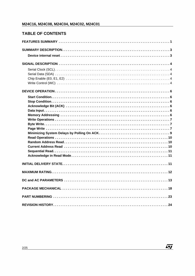
SUMMARY DESCRIPTIONThese I²C-compatible electrically erasable pro-grammable memory (EEPROM) devices are orga-nized as 2048/1024/512/256/128 x 8 (M24C16,M24C08, M24C04, M24C02 and M24C01).In order to meet environmental requirements, SToffers these devices in ECOPACK® packages.ECOPACK® packages are Lead-free and RoHScompliant. ECOPACK is an ST trademark. ECOPACK speci-fications are available at: www.st.com.
Figure 2. Logic Diagram
I²C uses a two-wire serial interface, comprising abi-directional data line and a clock line. The devic-es carry a built-in 4-bit Device Type Identifier code(1010) in accordance with the I²C bus definition.The device behaves as a slave in the I²C protocol,with all memory operations synchronized by theserial clock. Read and Write operations are initiat-ed by a Start condition, generated by the bus mas-ter. The Start condition is followed by a DeviceSelect Code and Read/Write bit (RW) (as de-
scribed in Table 3.), terminated by an acknowl-edge bit.When writing data to the memory, the device in-serts an acknowledge bit during the 9th bit time,following the bus master’s 8-bit transmission.When data is read by the bus master, the busmaster acknowledges the receipt of the data bytein the same way. Data transfers are terminated bya Stop condition after an Ack for Write, and after aNoAck for Read.
Table 2. Signal Names
Device internal resetIn order to prevent inadvertent Write operationsduring Power-up, a Power On Reset (POR) circuitis included. At Power-up (continuous rise of VCC),the device will not respond to any instructions untilthe VCC has reached the Power On Resetthreshold voltage (this threshold is lower than theVCC min. operating voltage defined in DC and ACPARAMETERS). When VCC has passed over thePOR threshold, the device is reset and is inStandby Power mode. At Power-down(continuous decay of VCC), as soon as VCC dropsfrom the normal operating voltage to below thePower On Reset threshold voltage, the devicestops responding to any instruction sent to it.Prior to selecting and issuing instructions to thememory, a valid and stable VCC voltage must beapplied. This voltage must remain stable and validuntil the end of the transmission of the instructionand, for a Write instruction, until the completion ofthe internal write cycle (tW).
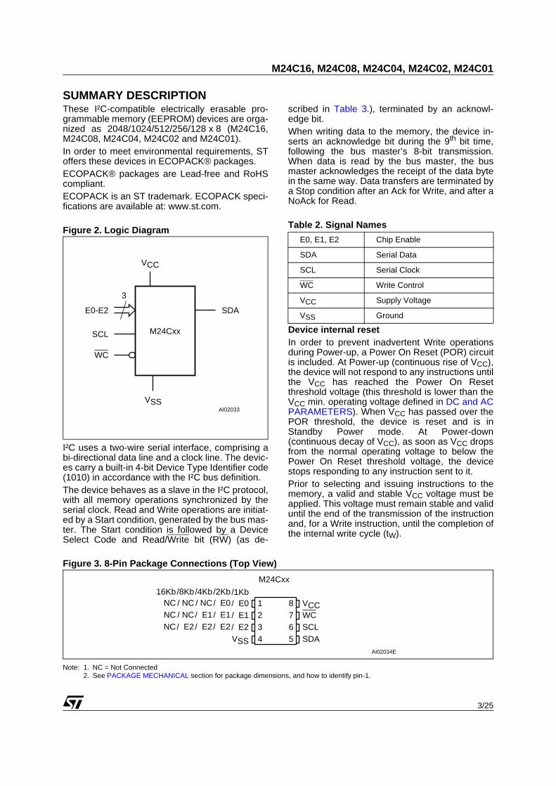
Figure 3. 8-Pin Package Connections (Top View)
Note: 1. NC = Not Connected2. See PACKAGE MECHANICAL section for package dimensions, and how to identify pin-1.
AI02033
3
E0-E2 SDA
VCC
M24Cxx
WC
SCL
VSS
E0, E1, E2 Chip Enable
SDA Serial Data
SCL Serial Clock
WC Write Control
VCC Supply Voltage
VSS Ground
SDAVSS
SCLWCVCC
/ E2
AI02034E
M24Cxx
1234
8765
/ E2/ E2/ E2NC/ E1/ E1/ E1/ NCNC/ E0/ E0/ NC/ NCNC/1Kb/2Kb/4Kb/8Kb16Kb
M24C16, M24C08, M24C04, M24C02, M24C01
4/25
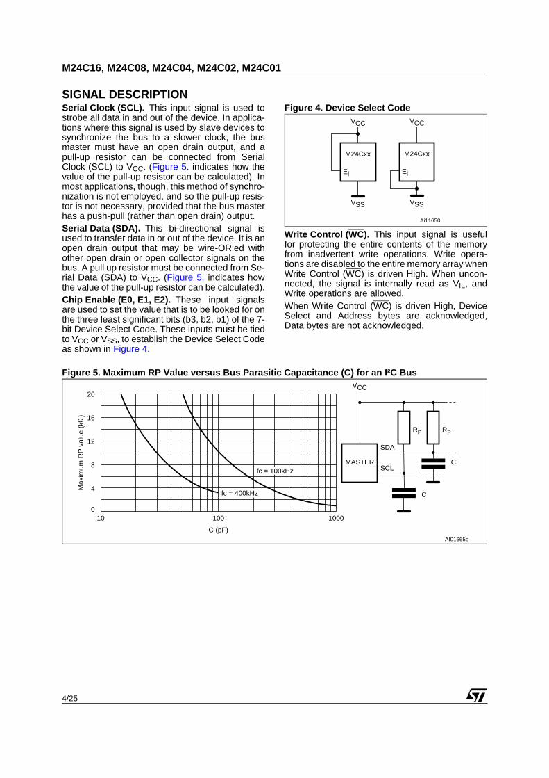
SIGNAL DESCRIPTIONSerial Clock (SCL). This input signal is used tostrobe all data in and out of the device. In applica-tions where this signal is used by slave devices tosynchronize the bus to a slower clock, the busmaster must have an open drain output, and apull-up resistor can be connected from SerialClock (SCL) to VCC. (Figure 5. indicates how thevalue of the pull-up resistor can be calculated). Inmost applications, though, this method of synchro-nization is not employed, and so the pull-up resis-tor is not necessary, provided that the bus masterhas a push-pull (rather than open drain) output.Serial Data (SDA). This bi-directional signal isused to transfer data in or out of the device. It is anopen drain output that may be wire-OR’ed withother open drain or open collector signals on thebus. A pull up resistor must be connected from Se-rial Data (SDA) to VCC. (Figure 5. indicates howthe value of the pull-up resistor can be calculated).Chip Enable (E0, E1, E2). These input signalsare used to set the value that is to be looked for onthe three least significant bits (b3, b2, b1) of the 7-bit Device Select Code. These inputs must be tiedto VCC or VSS, to establish the Device Select Codeas shown in Figure 4.
Figure 4. Device Select Code
Write Control (WC). This input signal is usefulfor protecting the entire contents of the memoryfrom inadvertent write operations. Write opera-tions are disabled to the entire memory array whenWrite Control (WC) is driven High. When uncon-nected, the signal is internally read as VIL, andWrite operations are allowed.When Write Control (WC) is driven High, DeviceSelect and Address bytes are acknowledged,Data bytes are not acknowledged.
Figure 5. Maximum RP Value versus Bus Parasitic Capacitance (C) for an I²C Bus
Ai11650
VCC
M24Cxx
VSS
Ei
VCC
M24Cxx
VSS
Ei
AI01665b
VCC
C
SDA
RP
MASTER
RP
SCLC
1000
4
8
12
16
20
C (pF)
Max
imum
RP
val
ue (
kΩ)
10 1000
fc = 400kHz
fc = 100kHz
5/25
M24C16, M24C08, M24C04, M24C02, M24C01
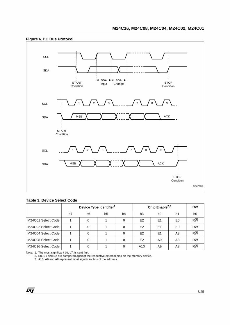
Figure 6. I²C Bus Protocol
Table 3. Device Select Code
Note: 1. The most significant bit, b7, is sent first.2. E0, E1 and E2 are compared against the respective external pins on the memory device.3. A10, A9 and A8 represent most significant bits of the address.
Device Type Identifier1 Chip Enable2,3 RW
b7 b6 b5 b4 b3 b2 b1 b0
M24C01 Select Code 1 0 1 0 E2 E1 E0 RW
M24C02 Select Code 1 0 1 0 E2 E1 E0 RW
M24C04 Select Code 1 0 1 0 E2 E1 A8 RW
M24C08 Select Code 1 0 1 0 E2 A9 A8 RW
M24C16 Select Code 1 0 1 0 A10 A9 A8 RW
SCL
SDA
SCL
SDA
SDA
STARTCondition
SDAInput
SDAChange
AI00792B
STOPCondition
1 2 3 7 8 9
MSB ACK
STARTCondition
SCL 1 2 3 7 8 9
MSB ACK
STOPCondition
M24C16, M24C08, M24C04, M24C02, M24C01
6/25
DEVICE OPERATION The device supports the I²C protocol. This is sum-marized in Figure 6.. Any device that sends dataon to the bus is defined to be a transmitter, andany device that reads the data to be a receiver.The device that controls the data transfer is knownas the bus master, and the other as the slave de-vice. A data transfer can only be initiated by thebus master, which will also provide the serial clockfor synchronization. The M24Cxx device is alwaysa slave in all communication.Start ConditionStart is identified by a falling edge of Serial Data(SDA) while Serial Clock (SCL) is stable in theHigh state. A Start condition must precede anydata transfer command. The device continuouslymonitors (except during a Write cycle) Serial Data(SDA) and Serial Clock (SCL) for a Start condition,and will not respond unless one is given.Stop ConditionStop is identified by a rising edge of Serial Data(SDA) while Serial Clock (SCL) is stable and driv-en High. A Stop condition terminates communica-tion between the device and the bus master. ARead command that is followed by NoAck can befollowed by a Stop condition to force the deviceinto the Stand-by mode. A Stop condition at theend of a Write command triggers the internal Writecycle.Acknowledge Bit (ACK)The acknowledge bit is used to indicate a success-ful byte transfer. The bus transmitter, whether it bebus master or slave device, releases Serial Data(SDA) after sending eight bits of data. During the9th clock pulse period, the receiver pulls SerialData (SDA) Low to acknowledge the receipt of theeight data bits.Data InputDuring data input, the device samples Serial Data(SDA) on the rising edge of Serial Clock (SCL).For correct device operation, Serial Data (SDA)must be stable during the rising edge of Serial
Clock (SCL), and the Serial Data (SDA) signalmust change only when Serial Clock (SCL) is driv-en Low.Memory AddressingTo start communication between the bus masterand the slave device, the bus master must initiatea Start condition. Following this, the bus mastersends the Device Select Code, shown in Table 3.(on Serial Data (SDA), most significant bit first).The Device Select Code consists of a 4-bit DeviceType Identifier, and a 3-bit Chip Enable “Address”(E2, E1, E0). To address the memory array, the 4-bit Device Type Identifier is 1010b.Each device is given a unique 3-bit code on theChip Enable (E0, E1, E2) inputs. When the DeviceSelect Code is received, the device only respondsif the Chip Enable Address is the same as the val-ue on the Chip Enable (E0, E1, E2) inputs. How-ever, those devices with larger memory capacities(the M24C16, M24C08 and M24C04) need moreaddress bits. E0 is not available for use on devicesthat need to use address line A8; E1 is not avail-able for devices that need to use address line A9,and E2 is not available for devices that need to useaddress line A10 (see Figure 3. and Table 3. fordetails). Using the E0, E1 and E2 inputs, up toeight M24C02 (or M24C01), four M24C04, twoM24C08 or one M24C16 devices can be connect-ed to one I²C bus. In each case, and in the hybridcases, this gives a total memory capacity of16 Kbits, 2 KBytes (except where M24C01 devic-es are used).The 8th bit is the Read/Write bit (RW). This bit isset to 1 for Read and 0 for Write operations.If a match occurs on the Device Select code, thecorresponding device gives an acknowledgmenton Serial Data (SDA) during the 9th bit time. If thedevice does not match the Device Select code, itdeselects itself from the bus, and goes into Stand-by mode.
Table 4. Operating Modes
Note: 1. X = VIH or VIL.
Mode RW bit WC 1 Bytes Initial Sequence
Current Address Read 1 X 1 START, Device Select, RW = 1
Random Address Read0 X
1START, Device Select, RW = 0, Address
1 X reSTART, Device Select, RW = 1
Sequential Read 1 X ≥ 1 Similar to Current or Random Address Read
Byte Write 0 VIL 1 START, Device Select, RW = 0
Page Write 0 VIL ≤ 16 START, Device Select, RW = 0
7/25
M24C16, M24C08, M24C04, M24C02, M24C01
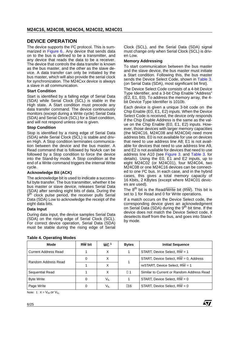
Figure 7. Write Mode Sequences with WC=1 (data write inhibited)
Write Operations Following a Start condition the bus master sendsa Device Select Code with the Read/Write bit(RW) reset to 0. The device acknowledges this, asshown in Figure 8., and waits for an address byte.The device responds to the address byte with anacknowledge bit, and then waits for the data byte.When the bus master generates a Stop conditionimmediately after the Ack bit (in the “10th bit” timeslot), either at the end of a Byte Write or a PageWrite, the internal Write cycle is triggered. A Stopcondition at any other time slot does not trigger theinternal Write cycle.During the internal Write cycle, Serial Data (SDA)and Serial Clock (SCL) are ignored, and the de-vice does not respond to any requests.Byte WriteAfter the Device Select code and the address byte,the bus master sends one data byte. If the ad-dressed location is Write-protected, by Write Con-trol (WC) being driven High (during the period from
the Start condition until the end of the addressbyte), the device replies to the data byte withNoAck, as shown in Figure 7., and the location isnot modified. If, instead, the addressed location isnot Write-protected, the device replies with Ack.The bus master terminates the transfer by gener-ating a Stop condition, as shown in Figure 8..Page WriteThe Page Write mode allows up to 16 bytes to bewritten in a single Write cycle, provided that theyare all located in the same page in the memory:that is, the most significant memory address bitsare the same. If more bytes are sent than will fit upto the end of the page, a condition known as ‘roll-over’ occurs. This should be avoided, as datastarts to become overwritten in an implementationdependent way.The bus master sends from 1 to 16 bytes of data,each of which is acknowledged by the device ifWrite Control (WC) is Low. If the addressed loca-tion is Write-protected, by Write Control (WC) be-ing driven High (during the period from the Start
ST
OP
ST
AR
T
Byte Write DEV SEL BYTE ADDR DATA IN
WC
ST
AR
T
Page Write DEV SEL BYTE ADDR DATA IN 1 DATA IN 2
WC
DATA IN 3
AI02803C
Page Write(cont'd)
WC (cont'd)
ST
OP
DATA IN N
ACK ACK NO ACK
R/W
ACK ACK NO ACK NO ACK
R/W
NO ACK NO ACK
M24C16, M24C08, M24C04, M24C02, M24C01
8/25
condition until the end of the address byte), the de-vice replies to the data bytes with NoAck, asshown in Figure 7., and the locations are not mod-ified. After each byte is transferred, the internal
byte address counter (the 4 least significant ad-dress bits only) is incremented. The transfer is ter-minated by the bus master generating a Stopcondition.
Figure 8. Write Mode Sequences with WC=0 (data write enabled)
ST
OP
ST
AR
T
BYTE WRITE DEV SEL BYTE ADDR DATA IN
WC
ST
AR
T
PAGE WRITE DEV SEL BYTE ADDR DATA IN 1 DATA IN 2
WC
DATA IN 3
AI02804B
PAGE WRITE(cont'd)
WC (cont'd)
ST
OP
DATA IN N
ACK
R/W
ACK ACK
ACK ACK ACK ACK
R/W
ACKACK
9/25
M24C16, M24C08, M24C04, M24C02, M24C01
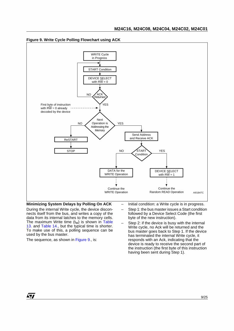
Figure 9. Write Cycle Polling Flowchart using ACK
Minimizing System Delays by Polling On ACKDuring the internal Write cycle, the device discon-nects itself from the bus, and writes a copy of thedata from its internal latches to the memory cells.The maximum Write time (tw) is shown in Table13. and Table 14., but the typical time is shorter.To make use of this, a polling sequence can beused by the bus master. The sequence, as shown in Figure 9., is:
– Initial condition: a Write cycle is in progress.– Step 1: the bus master issues a Start condition
followed by a Device Select Code (the first byte of the new instruction).
– Step 2: if the device is busy with the internal Write cycle, no Ack will be returned and the bus master goes back to Step 1. If the device has terminated the internal Write cycle, it responds with an Ack, indicating that the device is ready to receive the second part of the instruction (the first byte of this instruction having been sent during Step 1).
WRITE Cyclein Progress
AI01847C
NextOperation is
Addressing theMemory
START Condition
DEVICE SELECTwith RW = 0
ACKReturned
YES
NO
YESNO
ReSTART
STOP
DATA for theWRITE Operation
DEVICE SELECTwith RW = 1
Send Addressand Receive ACK
First byte of instructionwith RW = 0 alreadydecoded by the device
YESNO STARTCondition
Continue theWRITE Operation
Continue theRandom READ Operation
M24C16, M24C08, M24C04, M24C02, M24C01
10/25
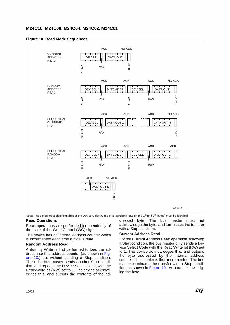
Figure 10. Read Mode Sequences
Note: The seven most significant bits of the Device Select Code of a Random Read (in the 1st and 3rd bytes) must be identical.
Read OperationsRead operations are performed independently ofthe state of the Write Control (WC) signal.The device has an internal address counter whichis incremented each time a byte is read.Random Address ReadA dummy Write is first performed to load the ad-dress into this address counter (as shown in Fig-ure 10.) but without sending a Stop condition.Then, the bus master sends another Start condi-tion, and repeats the Device Select Code, with theRead/Write bit (RW) set to 1. The device acknowl-edges this, and outputs the contents of the ad-
dressed byte. The bus master must notacknowledge the byte, and terminates the transferwith a Stop condition.Current Address ReadFor the Current Address Read operation, followinga Start condition, the bus master only sends a De-vice Select Code with the Read/Write bit (RW) setto 1. The device acknowledges this, and outputsthe byte addressed by the internal addresscounter. The counter is then incremented. The busmaster terminates the transfer with a Stop condi-tion, as shown in Figure 10., without acknowledg-ing the byte.
ST
AR
T
DEV SEL * BYTE ADDR
ST
AR
T
DEV SEL DATA OUT 1
AI01942
DATA OUT N
ST
OP
ST
AR
T
CURRENTADDRESSREAD
DEV SEL DATA OUT
RANDOMADDRESSREAD
ST
OP
ST
AR
T
DEV SEL * DATA OUT
SEQUENTIALCURRENTREAD
ST
OP
DATA OUT N
ST
AR
T
DEV SEL * BYTE ADDRSEQUENTIALRANDOMREAD
ST
AR
T
DEV SEL * DATA OUT 1
ST
OP
ACK
R/W
NO ACK
ACK
R/W
ACK ACK
R/W
ACK ACK ACK NO ACK
R/W
NO ACK
ACK ACK
R/W
ACK ACK
R/W
ACK NO ACK
11/25
M24C16, M24C08, M24C04, M24C02, M24C01
Sequential ReadThis operation can be used after a Current Ad-dress Read or a Random Address Read. The busmaster does acknowledge the data byte output,and sends additional clock pulses so that the de-vice continues to output the next byte in sequence.To terminate the stream of bytes, the bus mastermust not acknowledge the last byte, and mustgenerate a Stop condition, as shown in Figure 10..The output data comes from consecutive address-es, with the internal address counter automaticallyincremented after each byte output. After the lastmemory address, the address counter ‘rolls-over’,and the device continues to output data frommemory address 00h.
Acknowledge in Read ModeFor all Read commands, the device waits, aftereach byte read, for an acknowledgment during the9th bit time. If the bus master does not drive SerialData (SDA) Low during this time, the device termi-nates the data transfer and switches to its Stand-by mode.
INITIAL DELIVERY STATEThe device is delivered with all bits in the memoryarray set to 1 (each byte contains FFh).
M24C16, M24C08, M24C04, M24C02, M24C01
12/25
MAXIMUM RATINGStressing the device outside the ratings listed inTable 5. may cause permanent damage to the de-vice. These are stress ratings only, and operationof the device at these, or any other conditions out-side those indicated in the Operating sections of
this specification, is not implied. Exposure to Ab-solute Maximum Rating conditions for extendedperiods may affect device reliability. Refer also tothe STMicroelectronics SURE Program and otherrelevant quality documents.
Table 5. Absolute Maximum Ratings
Note: 1. Compliant with JEDEC Std J-STD-020C (for small body, Sn-Pb or Pb assembly), the ST ECOPACK® 7191395 specification, andthe European directive on Restrictions on Hazardous Substances (RoHS) 2002/95/EU
2. AEC-Q100-002 (compliant with JEDEC Std JESD22-A114A, C1=100pF, R1=1500Ω, R2=500Ω)
Symbol Parameter Min. Max. Unit
TA Ambient Operating Temperature –40 125 °C
TSTG Storage Temperature –65 150 °C
TLEAD Lead Temperature during Soldering 1 °C
VIO Input or Output range –0.50 6.5 V
VCC Supply Voltage –0.50 6.5 V
VESD Electrostatic Discharge Voltage (Human Body model) 2 –4000 4000 V
13/25
M24C16, M24C08, M24C04, M24C02, M24C01
DC AND AC PARAMETERSThis section summarizes the operating and mea-surement conditions, and the DC and AC charac-teristics of the device. The parameters in the DCand AC Characteristic tables that follow are de-rived from tests performed under the Measure-
ment Conditions summarized in the relevanttables. Designers should check that the operatingconditions in their circuit match the measurementconditions when relying on the quoted parame-ters.
Table 6. Operating Conditions (M24Cxx-W)
Table 7. Operating Conditions (M24Cxx-R)
Table 8. DC Characteristics (M24Cxx-W, Device Grade 6)
Note: 1. The voltage source driving only E0, E1 and E2 inputs must provide an impedance of less than 1kOhm.
Symbol Parameter Min. Max. Unit
VCC Supply Voltage 2.5 5.5 V
TA
Ambient Operating Temperature (Device Grade 6) –40 85 °C
Ambient Operating Temperature (Device Grade 3) –40 125 °C
Symbol Parameter Min. Max. Unit
VCC Supply Voltage 1.8 5.5 V
TA Ambient Operating Temperature –40 85 °C
Symbol Parameter Test Condition(in addition to those in Table 6.) Min. Max. Unit
ILIInput Leakage Current(SCL, SDA, E0, E1,and E2)
VIN = VSS or VCC ± 2 µA
ILO Output Leakage Current VOUT = VSS or VCC, SDA in Hi-Z ± 2 µA
ICC Supply CurrentVCC=5V, fc=400kHz (rise/fall time < 30ns) 2 mA
VCC =2.5V, fc=400kHz (rise/fall time < 30ns) 1 mA
ICC1 Stand-by Supply CurrentVIN = VSS or VCC , VCC = 5 V 1 µA
VIN = VSS or VCC , VCC = 2.5 V 0.5 µA
VIL Input Low Voltage (1) –0.45 0.3VCC V
VIH Input High Voltage (1) 0.7VCC VCC+1 V
VOL Output Low Voltage IOL = 2.1 mA, VCC = 2.5 V 0.4 V
M24C16, M24C08, M24C04, M24C02, M24C01
14/25
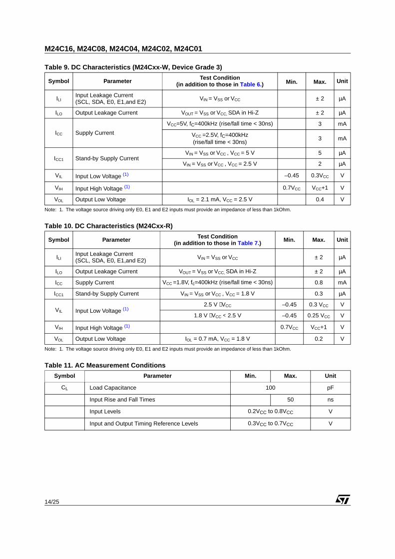
Table 9. DC Characteristics (M24Cxx-W, Device Grade 3)
Note: 1. The voltage source driving only E0, E1 and E2 inputs must provide an impedance of less than 1kOhm.
Table 10. DC Characteristics (M24Cxx-R)
Note: 1. The voltage source driving only E0, E1 and E2 inputs must provide an impedance of less than 1kOhm.
Table 11. AC Measurement Conditions
Symbol Parameter Test Condition(in addition to those in Table 6.) Min. Max. Unit
ILIInput Leakage Current(SCL, SDA, E0, E1,and E2)
VIN = VSS or VCC ± 2 µA
ILO Output Leakage Current VOUT = VSS or VCC, SDA in Hi-Z ± 2 µA
ICC Supply Current
VCC=5V, fC=400kHz (rise/fall time < 30ns) 3 mA
VCC =2.5V, fC=400kHz (rise/fall time < 30ns)
3 mA
ICC1 Stand-by Supply CurrentVIN = VSS or VCC , VCC = 5 V 5 µA
VIN = VSS or VCC , VCC = 2.5 V 2 µA
VIL Input Low Voltage (1) –0.45 0.3VCC V
VIH Input High Voltage (1) 0.7VCC VCC+1 V
VOL Output Low Voltage IOL = 2.1 mA, VCC = 2.5 V 0.4 V
Symbol Parameter Test Condition(in addition to those in Table 7.) Min. Max. Unit
ILIInput Leakage Current(SCL, SDA, E0, E1,and E2)
VIN = VSS or VCC ± 2 µA
ILO Output Leakage Current VOUT = VSS or VCC, SDA in Hi-Z ± 2 µA
ICC Supply Current VCC =1.8V, fc=400kHz (rise/fall time < 30ns) 0.8 mA
ICC1 Stand-by Supply Current VIN = VSS or VCC , VCC = 1.8 V 0.3 µA
VIL Input Low Voltage (1)2.5 V ≤ VCC –0.45 0.3 VCC V
1.8 V ≤ VCC < 2.5 V –0.45 0.25 VCC V
VIH Input High Voltage (1) 0.7VCC VCC+1 V
VOL Output Low Voltage IOL = 0.7 mA, VCC = 1.8 V 0.2 V
Symbol Parameter Min. Max. Unit
CL Load Capacitance 100 pF
Input Rise and Fall Times 50 ns
Input Levels 0.2VCC to 0.8VCC V
Input and Output Timing Reference Levels 0.3VCC to 0.7VCC V
15/25
M24C16, M24C08, M24C04, M24C02, M24C01
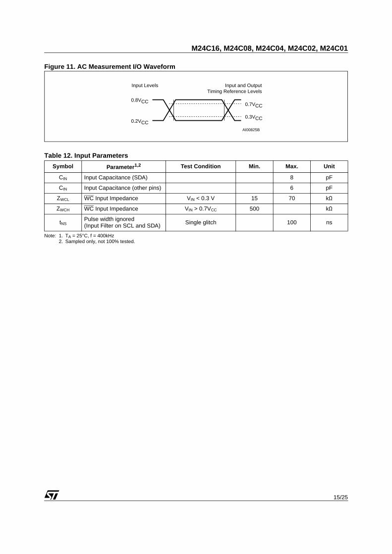
Figure 11. AC Measurement I/O Waveform
Table 12. Input Parameters
Note: 1. TA = 25°C, f = 400kHz2. Sampled only, not 100% tested.
Symbol Parameter1,2 Test Condition Min. Max. Unit
CIN Input Capacitance (SDA) 8 pF
CIN Input Capacitance (other pins) 6 pF
ZWCL WC Input Impedance VIN < 0.3 V 15 70 kΩ
ZWCH WC Input Impedance VIN > 0.7VCC 500 kΩ
tNSPulse width ignored(Input Filter on SCL and SDA) Single glitch 100 ns
AI00825B
0.8VCC
0.2VCC
0.7VCC
0.3VCC
Input and OutputTiming Reference Levels
Input Levels
M24C16, M24C08, M24C04, M24C02, M24C01
16/25
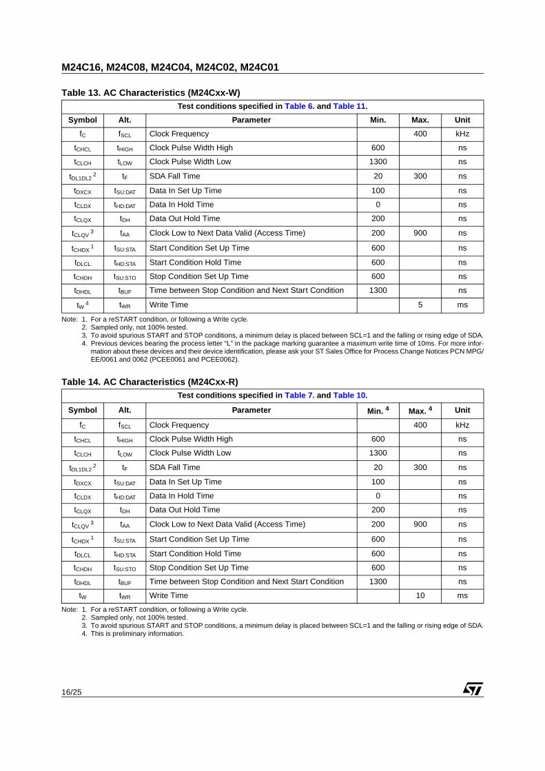
Table 13. AC Characteristics (M24Cxx-W)
Note: 1. For a reSTART condition, or following a Write cycle.2. Sampled only, not 100% tested.3. To avoid spurious START and STOP conditions, a minimum delay is placed between SCL=1 and the falling or rising edge of SDA.4. Previous devices bearing the process letter “L” in the package marking guarantee a maximum write time of 10ms. For more infor-
mation about these devices and their device identification, please ask your ST Sales Office for Process Change Notices PCN MPG/EE/0061 and 0062 (PCEE0061 and PCEE0062).
Table 14. AC Characteristics (M24Cxx-R)
Note: 1. For a reSTART condition, or following a Write cycle.2. Sampled only, not 100% tested.3. To avoid spurious START and STOP conditions, a minimum delay is placed between SCL=1 and the falling or rising edge of SDA.4. This is preliminary information.
Test conditions specified in Table 6. and Table 11.
Symbol Alt. Parameter Min. Max. Unit
fC fSCL Clock Frequency 400 kHz
tCHCL tHIGH Clock Pulse Width High 600 ns
tCLCH tLOW Clock Pulse Width Low 1300 ns
tDL1DL2 2 tF SDA Fall Time 20 300 ns
tDXCX tSU:DAT Data In Set Up Time 100 ns
tCLDX tHD:DAT Data In Hold Time 0 ns
tCLQX tDH Data Out Hold Time 200 ns
tCLQV 3 tAA Clock Low to Next Data Valid (Access Time) 200 900 ns
tCHDX 1 tSU:STA Start Condition Set Up Time 600 ns
tDLCL tHD:STA Start Condition Hold Time 600 ns
tCHDH tSU:STO Stop Condition Set Up Time 600 ns
tDHDL tBUF Time between Stop Condition and Next Start Condition 1300 ns
tW 4 tWR Write Time 5 ms
Test conditions specified in Table 7. and Table 10.
Symbol Alt. Parameter Min. 4 Max. 4 Unit
fC fSCL Clock Frequency 400 kHz
tCHCL tHIGH Clock Pulse Width High 600 ns
tCLCH tLOW Clock Pulse Width Low 1300 ns
tDL1DL2 2 tF SDA Fall Time 20 300 ns
tDXCX tSU:DAT Data In Set Up Time 100 ns
tCLDX tHD:DAT Data In Hold Time 0 ns
tCLQX tDH Data Out Hold Time 200 ns
tCLQV 3 tAA Clock Low to Next Data Valid (Access Time) 200 900 ns
tCHDX 1 tSU:STA Start Condition Set Up Time 600 ns
tDLCL tHD:STA Start Condition Hold Time 600 ns
tCHDH tSU:STO Stop Condition Set Up Time 600 ns
tDHDL tBUF Time between Stop Condition and Next Start Condition 1300 ns
tW tWR Write Time 10 ms
17/25
M24C16, M24C08, M24C04, M24C02, M24C01
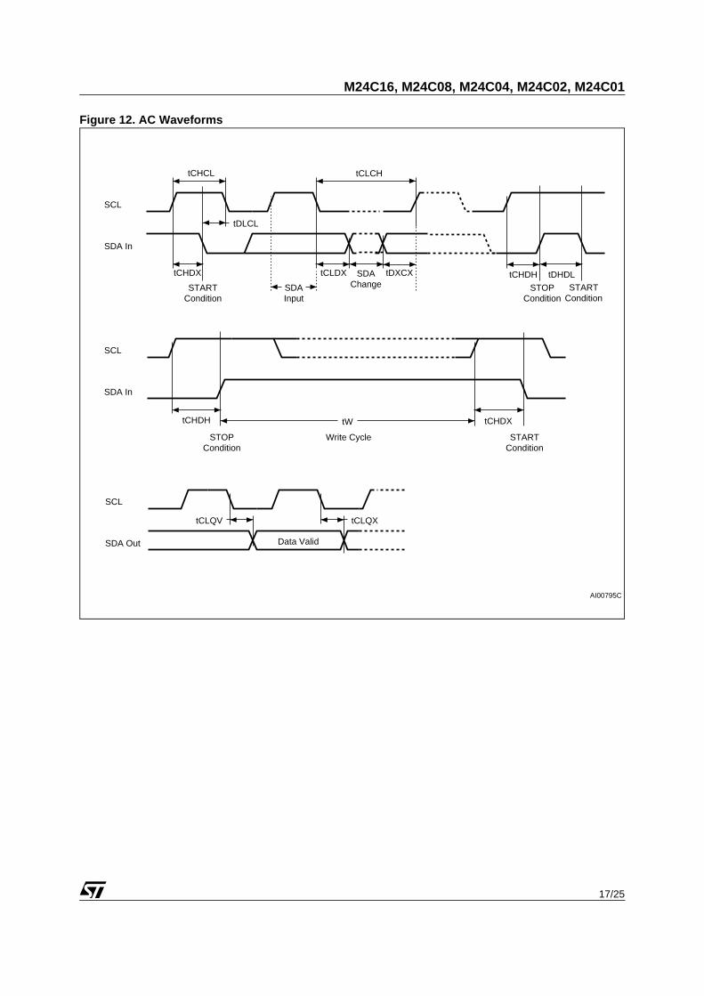
Figure 12. AC Waveforms
SCL
SDA In
SCL
SDA Out
SCL
SDA In
tCHCL
tDLCL
tCHDX
STARTCondition
tCLCH
tDXCXtCLDX
SDAInput
SDAChange
tCHDH tDHDL
STOPCondition
Data Valid
tCLQV tCLQX
tCHDH
STOPCondition
tCHDX
STARTCondition
Write Cycle
tW
AI00795C
STARTCondition
M24C16, M24C08, M24C04, M24C02, M24C01
18/25
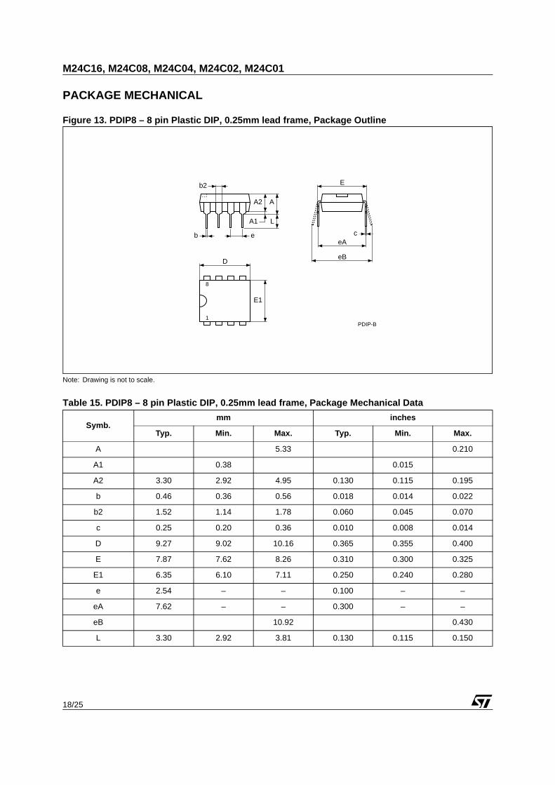
PACKAGE MECHANICAL
Figure 13. PDIP8 – 8 pin Plastic DIP, 0.25mm lead frame, Package Outline
Note: Drawing is not to scale.
Table 15. PDIP8 – 8 pin Plastic DIP, 0.25mm lead frame, Package Mechanical Data
Symb.mm inches
Typ. Min. Max. Typ. Min. Max.
A 5.33 0.210
A1 0.38 0.015
A2 3.30 2.92 4.95 0.130 0.115 0.195
b 0.46 0.36 0.56 0.018 0.014 0.022
b2 1.52 1.14 1.78 0.060 0.045 0.070
c 0.25 0.20 0.36 0.010 0.008 0.014
D 9.27 9.02 10.16 0.365 0.355 0.400
E 7.87 7.62 8.26 0.310 0.300 0.325
E1 6.35 6.10 7.11 0.250 0.240 0.280
e 2.54 – – 0.100 – –
eA 7.62 – – 0.300 – –
eB 10.92 0.430
L 3.30 2.92 3.81 0.130 0.115 0.150
PDIP-B
A2
A1
A
L
b e
D
E1
8
1
ceA
b2
eB
E
19/25
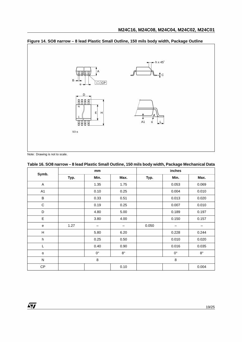
M24C16, M24C08, M24C04, M24C02, M24C01
Figure 14. SO8 narrow – 8 lead Plastic Small Outline, 150 mils body width, Package Outline
Note: Drawing is not to scale.
Table 16. SO8 narrow – 8 lead Plastic Small Outline, 150 mils body width, Package Mechanical Data
Symb.mm inches
Typ. Min. Max. Typ. Min. Max.
A 1.35 1.75 0.053 0.069
A1 0.10 0.25 0.004 0.010
B 0.33 0.51 0.013 0.020
C 0.19 0.25 0.007 0.010
D 4.80 5.00 0.189 0.197
E 3.80 4.00 0.150 0.157
e 1.27 – – 0.050 – –
H 5.80 6.20 0.228 0.244
h 0.25 0.50 0.010 0.020
L 0.40 0.90 0.016 0.035
α 0° 8° 0° 8°
N 8 8
CP 0.10 0.004
SO-a
E
N
CPB
e
A
D
C
LA1 α
1
H
h x 45˚
M24C16, M24C08, M24C04, M24C02, M24C01
20/25
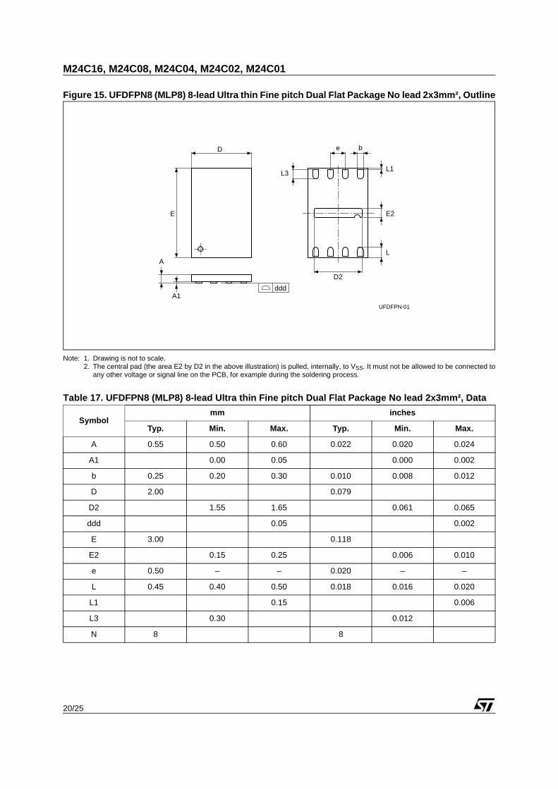
Figure 15. UFDFPN8 (MLP8) 8-lead Ultra thin Fine pitch Dual Flat Package No lead 2x3mm², Outline
Note: 1. Drawing is not to scale.2. The central pad (the area E2 by D2 in the above illustration) is pulled, internally, to VSS. It must not be allowed to be connected to
any other voltage or signal line on the PCB, for example during the soldering process.
Table 17. UFDFPN8 (MLP8) 8-lead Ultra thin Fine pitch Dual Flat Package No lead 2x3mm², Data
Symbolmm inches
Typ. Min. Max. Typ. Min. Max.
A 0.55 0.50 0.60 0.022 0.020 0.024
A1 0.00 0.05 0.000 0.002
b 0.25 0.20 0.30 0.010 0.008 0.012
D 2.00 0.079
D2 1.55 1.65 0.061 0.065
ddd 0.05 0.002
E 3.00 0.118
E2 0.15 0.25 0.006 0.010
e 0.50 – – 0.020 – –
L 0.45 0.40 0.50 0.018 0.016 0.020
L1 0.15 0.006
L3 0.30 0.012
N 8 8
D
E
UFDFPN-01
A
A1ddd
L1
e b
D2
L
E2
L3
21/25
M24C16, M24C08, M24C04, M24C02, M24C01
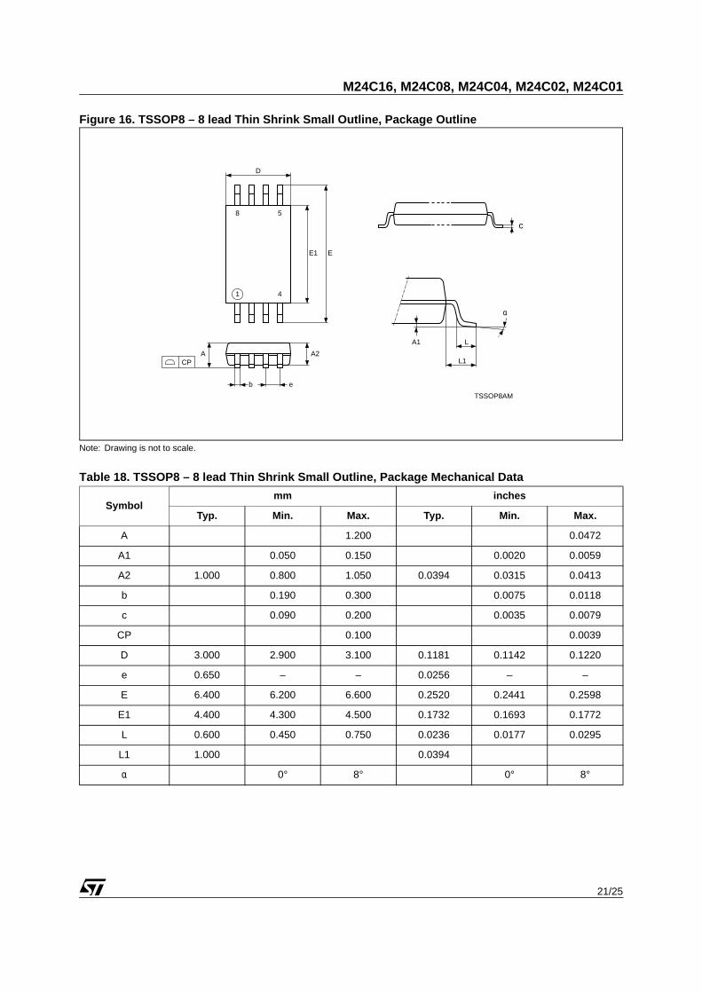
Figure 16. TSSOP8 – 8 lead Thin Shrink Small Outline, Package Outline
Note: Drawing is not to scale.
Table 18. TSSOP8 – 8 lead Thin Shrink Small Outline, Package Mechanical Data
Symbolmm inches
Typ. Min. Max. Typ. Min. Max.
A 1.200 0.0472
A1 0.050 0.150 0.0020 0.0059
A2 1.000 0.800 1.050 0.0394 0.0315 0.0413
b 0.190 0.300 0.0075 0.0118
c 0.090 0.200 0.0035 0.0079
CP 0.100 0.0039
D 3.000 2.900 3.100 0.1181 0.1142 0.1220
e 0.650 – – 0.0256 – –
E 6.400 6.200 6.600 0.2520 0.2441 0.2598
E1 4.400 4.300 4.500 0.1732 0.1693 0.1772
L 0.600 0.450 0.750 0.0236 0.0177 0.0295
L1 1.000 0.0394
α 0° 8° 0° 8°
TSSOP8AM
1
8
CP
c
L
EE1
D
A2A
α
eb
4
5
A1
L1
M24C16, M24C08, M24C04, M24C02, M24C01
22/25
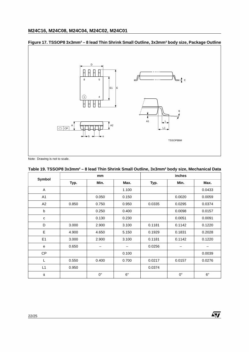
Figure 17. TSSOP8 3x3mm² – 8 lead Thin Shrink Small Outline, 3x3mm² body size, Package Outline
Note: Drawing is not to scale.
Table 19. TSSOP8 3x3mm² – 8 lead Thin Shrink Small Outline, 3x3mm² body size, Mechanical Data
Symbolmm inches
Typ. Min. Max. Typ. Min. Max.
A 1.100 0.0433
A1 0.050 0.150 0.0020 0.0059
A2 0.850 0.750 0.950 0.0335 0.0295 0.0374
b 0.250 0.400 0.0098 0.0157
c 0.130 0.230 0.0051 0.0091
D 3.000 2.900 3.100 0.1181 0.1142 0.1220
E 4.900 4.650 5.150 0.1929 0.1831 0.2028
E1 3.000 2.900 3.100 0.1181 0.1142 0.1220
e 0.650 – – 0.0256 – –
CP 0.100 0.0039
L 0.550 0.400 0.700 0.0217 0.0157 0.0276
L1 0.950 0.0374
α 0° 6° 0° 6°
TSSOP8BM
1
8
CP
c
L
EE1
D
A2A
α
eb
4
5
A1
L1
23/25
M24C16, M24C08, M24C04, M24C02, M24C01
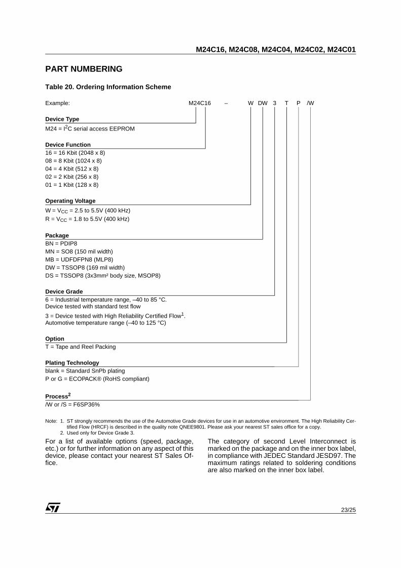
PART NUMBERING
Table 20. Ordering Information Scheme
Note: 1. ST strongly recommends the use of the Automotive Grade devices for use in an automotive environment. The High Reliability Cer-tified Flow (HRCF) is described in the quality note QNEE9801. Please ask your nearest ST sales office for a copy.
2. Used only for Device Grade 3.
For a list of available options (speed, package,etc.) or for further information on any aspect of thisdevice, please contact your nearest ST Sales Of-fice.
The category of second Level Interconnect ismarked on the package and on the inner box label,in compliance with JEDEC Standard JESD97. Themaximum ratings related to soldering conditionsare also marked on the inner box label.
Example: M24C16 – W DW 3 T P /W
Device Type
M24 = I2C serial access EEPROM
Device Function16 = 16 Kbit (2048 x 8)08 = 8 Kbit (1024 x 8)04 = 4 Kbit (512 x 8)02 = 2 Kbit (256 x 8)01 = 1 Kbit (128 x 8)
Operating Voltage
W = VCC = 2.5 to 5.5V (400 kHz)
R = VCC = 1.8 to 5.5V (400 kHz)
PackageBN = PDIP8MN = SO8 (150 mil width)MB = UDFDFPN8 (MLP8)DW = TSSOP8 (169 mil width)DS = TSSOP8 (3x3mm² body size, MSOP8)
Device Grade6 = Industrial temperature range, –40 to 85 °C.Device tested with standard test flow
3 = Device tested with High Reliability Certified Flow1.Automotive temperature range (–40 to 125 °C)
OptionT = Tape and Reel Packing
Plating Technologyblank = Standard SnPb platingP or G = ECOPACK® (RoHS compliant)
Process2
/W or /S = F6SP36%
M24C16, M24C08, M24C04, M24C02, M24C01
24/25
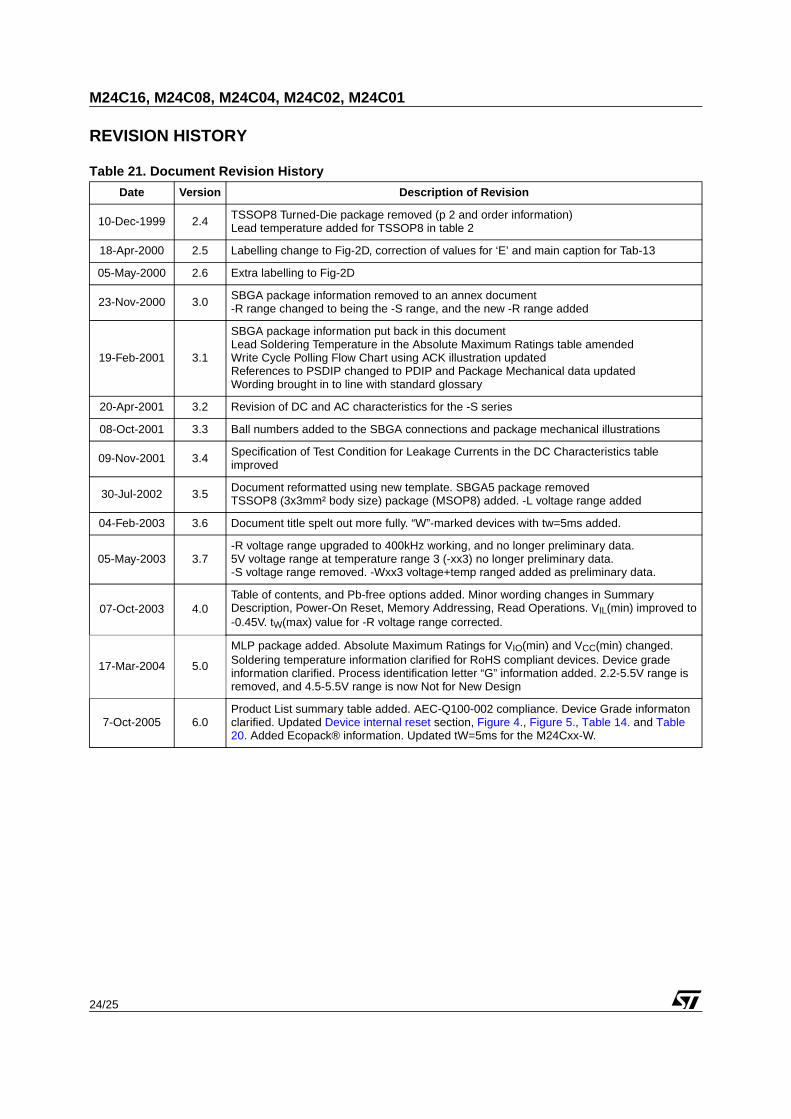
REVISION HISTORY
Table 21. Document Revision History
Date Version Description of Revision
10-Dec-1999 2.4 TSSOP8 Turned-Die package removed (p 2 and order information)Lead temperature added for TSSOP8 in table 2
18-Apr-2000 2.5 Labelling change to Fig-2D, correction of values for ‘E’ and main caption for Tab-13
05-May-2000 2.6 Extra labelling to Fig-2D
23-Nov-2000 3.0SBGA package information removed to an annex document-R range changed to being the -S range, and the new -R range added
19-Feb-2001 3.1
SBGA package information put back in this documentLead Soldering Temperature in the Absolute Maximum Ratings table amendedWrite Cycle Polling Flow Chart using ACK illustration updatedReferences to PSDIP changed to PDIP and Package Mechanical data updatedWording brought in to line with standard glossary
20-Apr-2001 3.2 Revision of DC and AC characteristics for the -S series
08-Oct-2001 3.3 Ball numbers added to the SBGA connections and package mechanical illustrations
09-Nov-2001 3.4 Specification of Test Condition for Leakage Currents in the DC Characteristics table improved
30-Jul-2002 3.5 Document reformatted using new template. SBGA5 package removedTSSOP8 (3x3mm² body size) package (MSOP8) added. -L voltage range added
04-Feb-2003 3.6 Document title spelt out more fully. “W”-marked devices with tw=5ms added.
05-May-2003 3.7-R voltage range upgraded to 400kHz working, and no longer preliminary data.5V voltage range at temperature range 3 (-xx3) no longer preliminary data.-S voltage range removed. -Wxx3 voltage+temp ranged added as preliminary data.
07-Oct-2003 4.0Table of contents, and Pb-free options added. Minor wording changes in Summary Description, Power-On Reset, Memory Addressing, Read Operations. VIL(min) improved to-0.45V. tW(max) value for -R voltage range corrected.
17-Mar-2004 5.0
MLP package added. Absolute Maximum Ratings for VIO(min) and VCC(min) changed. Soldering temperature information clarified for RoHS compliant devices. Device grade information clarified. Process identification letter “G” information added. 2.2-5.5V range is removed, and 4.5-5.5V range is now Not for New Design
7-Oct-2005 6.0Product List summary table added. AEC-Q100-002 compliance. Device Grade informaton clarified. Updated Device internal reset section, Figure 4., Figure 5., Table 14. and Table 20. Added Ecopack® information. Updated tW=5ms for the M24Cxx-W.
25/25
M24C16, M24C08, M24C04, M24C02, M24C01
Information furnished is believed to be accurate and reliable. However, STMicroelectronics assumes no responsibility for the consequences of use of such information nor for any infringement of patents or other rights of third parties which may result from its use. No license is granted by implication or otherwise under any patent or patent rights of STMicroelectronics. Specifications mentioned in this publication are subject to change without notice. This publication supersedes and replaces all information previously supplied. STMicroelectronics products are not
authorized for use as critical components in life support devices or systems without express written approval of STMicroelectronics.
The ST logo is a registered trademark of STMicroelectronics.
All other names are the property of their respective owners
© 2005 STMicroelectronics - All rights reserved
STMicroelectronics group of companiesAustralia - Belgium - Brazil - Canada - China - Czech Republic - Finland - France - Germany - Hong Kong - India - Israel - Italy - Japan -
Malaysia - Malta - Morocco - Singapore - Spain - Sweden - Switzerland - United Kingdom - United States of Americawww.st.com


