Embed Size (px)
Citation preview
1.65 GHz Clock Fanout Buffer with Output Dividers and Delay Adjust
Data Sheet AD9508
Rev. G Document Feedback Information furnished by Analog Devices is believed to be accurate and reliable. However, no responsibility is assumed by Analog Devices for its use, nor for any infringements of patents or other rights of third parties that may result from its use. Specifications subject to change without notice. No license is granted by implication or otherwise under any patent or patent rights of Analog Devices. Trademarks and registered trademarks are the property of their respective owners.
One Technology Way, P.O. Box 9106, Norwood, MA 02062-9106, U.S.A. Tel: 781.329.4700 ©2013–2017 Analog Devices, Inc. All rights reserved. Technical Support www.analog.com
FEATURES 1.65 GHz differential clock inputs/outputs 10-bit programmable dividers, 1 to 1024, all integers Up to 4 differential outputs or 8 CMOS outputs Pin strapping capability for hardwired programming at
power-up <115 fs rms broadband random jitter (see Figure 25) Additive output jitter: 41 fs rms typical (12 kHz to 20 MHz) Excellent output-to-output isolation Automatic synchronization of all outputs Single 2.5 V/3.3 V power supply Internal LDO (low drop-out) voltage regulator for enhanced
power supply immunity Phase offset select for output-to-output coarse delay adjust 3 programmable output logic levels, LVDS, HSTL, and CMOS Serial control port (SPI/I2C) or pin-programmable mode Space-saving 24-lead LFCSP
APPLICATIONS Low jitter, low phase noise clock distribution Clocking high speed ADCs, DACs, DDSs, DDCs, DUCs, MxFEs High performance wireless transceivers High performance instrumentation Broadband infrastructure
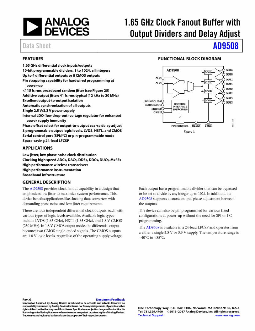
FUNCTIONAL BLOCK DIAGRAM
Figure 1.
GENERAL DESCRIPTION The AD9508 provides clock fanout capability in a design that emphasizes low jitter to maximize system performance. This device benefits applications like clocking data converters with demanding phase noise and low jitter requirements.
There are four independent differential clock outputs, each with various types of logic levels available. Available logic types include LVDS (1.65 GHz), HSTL (1.65 GHz), and 1.8 V CMOS (250 MHz). In 1.8 V CMOS output mode, the differential output becomes two CMOS single-ended signals. The CMOS outputs are 1.8 V logic levels, regardless of the operating supply voltage.
Each output has a programmable divider that can be bypassed or be set to divide by any integer up to 1024. In addition, the AD9508 supports a coarse output phase adjustment between the outputs.
The device can also be pin programmed for various fixed configurations at power-up without the need for SPI or I2C programming.
The AD9508 is available in a 24-lead LFCSP and operates from a either a single 2.5 V or 3.3 V supply. The temperature range is −40°C to +85°C.
DIV/ΦOUT0
OUT0
OUT1
OUT1
OUT2
OUT2
OUT3
OUT3CONTROLINTERFACESPI/I2C/PINS
AD9508
CLK
SCLK/SCL/S0SDIO/SDA/S1
SDO/S3CS/S2
SYNC
CLK
PIN CONTROL
DIV/Φ
DIV/Φ
DIV/Φ
RESET 1116
1-00
1

AD9508 Data Sheet
Rev. G | Page 2 of 40
TABLE OF CONTENTS Features .............................................................................................. 1 Applications ....................................................................................... 1 Functional Block Diagram .............................................................. 1 General Description ......................................................................... 1 Revision History ............................................................................... 3 Specifications ..................................................................................... 4
Electrical Characteristics ............................................................. 4 Power Supply Current and Temperature Conditions .............. 4 Clock Inputs and Output DC Specifications ............................ 5 Output Driver Timing Characteristics ...................................... 6 Logic Inputs ................................................................................... 7 Serial Port Specifications—SPI Mode ........................................ 7 Serial Port Specifications—I2C Mode ........................................ 8 External Resistor Values For Pin Strapping Mode ................... 9 Clock Output Additive Phase Noise .......................................... 9 Clock Output Additive Time Jitter ........................................... 10
Absolute Maximum Ratings .......................................................... 11 Thermal Characteristics ............................................................ 11 ESD Caution ................................................................................ 11
Pin Configuration and Function Descriptions ........................... 12 Typical Performance Characteristics ........................................... 14 Test Circuits ..................................................................................... 20
Input/Output Termination Recommendations ...................... 20 Terminology .................................................................................... 21 Theory of Operation ...................................................................... 22
Detailed Block Diagram ............................................................ 22 Programming Mode Selection .................................................. 22
Clock Input.................................................................................. 23 Clock Outputs ............................................................................. 24 Clock Dividers ............................................................................ 24 Phase Delay Control .................................................................. 24 Reset Modes ................................................................................ 25 Power-Down Mode .................................................................... 25 Output Clock Synchronization ................................................. 25 Power Supply ............................................................................... 25 Thermally Enhanced Package Mounting Guidelines ............ 25
Pin Strapping to Program on Power-Up ..................................... 26 Serial Control Port ......................................................................... 27
SPI/I2C Port Selection ................................................................ 27 SPI Serial Port Operation .......................................................... 27 I2C Serial Port Operation .......................................................... 30
Register Map ................................................................................... 33 Register Map Bit Descriptions ...................................................... 34
Serial Port Configuration (Register 0x00) .............................. 34 Silicon Revision (Register 0x0A to Register 0x0D) ............... 34 Chip Level Functions (Register 0x12 to Register 0x14) ........ 34 OUT0 Functions (Register 0x15 to Register 0x1A) ............... 35 OUT1 Functions (Register 0x1B to Register 0x20) ............... 36 OUT2 Functions (Register 0x21 to Register 0x26) ................ 37 OUT3 Functions (Register 0x27 to Register 0x2C) ............... 38
Packaging and Ordering Information ......................................... 40 Outline Dimensions ................................................................... 40 Ordering Guide .......................................................................... 40

Data Sheet AD9508
Rev. G | Page 3 of 40
REVISION HISTORY 6/2017—Rev. F to Rev. G Updated Outline Dimensions ........................................................ 40 Changes to Ordering Guide ........................................................... 40 4/2015—Rev. E to Rev. F Changes to Clock Outputs Section ............................................... 24 Changes to Table 28 ........................................................................ 35 Changes to Table 30 ........................................................................ 36 Changes to Table 32 ........................................................................ 38 Changes to Table 34 ........................................................................ 39 11/2014—Rev. D to Rev. E Changes to Figure 1 .......................................................................... 1 Moved Revision History Section ..................................................... 3 Changes to Table 12 ........................................................................ 12 Changes to Clock Outputs Section, Clock Dividers Section, and Phase Delay Control Section ......................................................... 24 Changed Individual Clock Channel Power-Down Section to Individual Clock Divider Power-Down Section ......................... 25 Changes to Individual Clock Divider Power-Down Section and Output Clock Synchronization Section ........................................ 25 Changes to Pin Strapping to Program on Power-up Section and Table 15 ............................................................................................. 26 Changes to Table 27 and Table 28 ................................................. 35 Changes to Table 29 and Table 30 ................................................. 36 Changes to Table 31 and Table 32 ................................................. 37 Changes to Table 33 ........................................................................ 38 Changes to Table 34 ........................................................................ 39 9/2014—Rev. C to Rev. D Changes to Table 1 ............................................................................ 3 Changes to Table 2 ............................................................................ 4 Changes to Figure 37 Caption; Added Figure 38; Renumbered Sequentially ...................................................................................... 19 Changes to Clock Input Section and Table 14 ............................. 23
2/2014—Rev. B to Rev. C Changes to Table 14 ........................................................................ 22 10/2013—Rev. A to Rev. B Change to Figure 5 Caption ........................................................... 13 Change to Figure 13 Caption ......................................................... 14 Change to Figure 19 Caption ......................................................... 15 Change to Individual Clock Channel Power-Down Section .... 23 Change to Write Section ................................................................ 27 Changes to Table 27 ........................................................................ 34 Changes to Table 29 ........................................................................ 35 Changes to Table 31 ........................................................................ 36 Changes to Table 33 ........................................................................ 37 4/2013—Rev. 0 to Rev. A Changes to Table 9 ............................................................................ 9 Changes to Figure 10 ...................................................................... 14 Changes to Figure 15 ...................................................................... 15 Changes to Figure 24 and Figure 26 ............................................. 16 Changes to Figure 27, Figure 29 to Figure 32.............................. 17 Changes to Figure 33 ...................................................................... 18 1/2013—Revision 0: Initial Version

AD9508 Data Sheet
Rev. G | Page 4 of 40
SPECIFICATIONS ELECTRICAL CHARACTERISTICS Typical values are given for VS = 3.3 V and 2.5 V and TA = 25°C; minimum and maximum values are given over the full VDD = 3.3 V + 5% down to 2.5 V − 5% and TA = −40°C to +85°C variation; and input slew rate > 1 V/ns, unless otherwise noted.
POWER SUPPLY CURRENT AND TEMPERATURE CONDITIONS
Table 1. Parameter Min Typ Max Unit Test Conditions/Comments SUPPLY VOLTAGE 2.375 2.5 3.465 V Use supply voltage setting (2.5 V or 3.3 V) and
appropriate current consumption configuration (see Current Consumption parameters in Table 1) to calculate total power dissipation
CURRENT CONSUMPTION LVDS Configuration 165 182 mA Input clock: 1500 MHz in differential mode, all
LVDS output drivers at 1500 MHz 122 134 mA Input clock: 800 MHz in differential mode, all
LVDS output drivers at 200 MHz HSTL Configuration 194 213 mA Input clock: 1500 MHz in differential mode, all
HSTL output drivers at 1500 MHz 131 144 mA Input clock: 491.52 MHz in differential mode, all
output drivers at 491.52 MHz 92 101 mA Input clock: 122.88 MHz in differential mode, all
output drivers at 122.88 MHz CMOS Configuration 141 185 mA Input clock: 1500 MHz in differential mode, all
CMOS output drivers at 250 MHz, 10 pF load 122 134 mA Input clock: 800 MHz in differential mode, all
CMOS outputs drivers at 200 MHz, 10 pF load 85 94 mA Input clock: 100 MHz in differential mode, all
CMOS outputs drivers at 100 MHz, 10 pF load Full Power-Down 6 10 mA
TEMPERATURE Ambient Temperature Range, TA −40 +25 +85 °C Junction Temperature, TJ 115 °C Junction temperatures above 115°C can
degrade performance but no damage should occur, unless the absolute temperature is exceeded

Data Sheet AD9508
Rev. G | Page 5 of 40
CLOCK INPUTS AND OUTPUT DC SPECIFICATIONS
Table 2. Parameter Symbol Min Typ Max Unit Test Conditions/Comments CLOCK INPUTS
Differential Mode Input Frequency 0 1650 MHz Differential input
Input Sensitivity 360 2200 mV p-p As measured with a differential probe; jitter performance improves with higher slew rates (greater voltage swing)
Input Common-Mode Voltage VICM 0.95 1.05 1.15 V Input pins are internally self biased, which enables ac coupling
Input Voltage Offset 30 mV DC-Coupled Input Common-
Mode Range VCMR 0.58 1.67 V This is the allowable common-mode
voltage range when dc-coupled Pulse Width
Low 303 ps High 303 ps
Input Resistance (Single-Ended) 5.0 7 9 kΩ Input Capacitance CIN 2 pF Input Bias Current (Each Pin) 100 400 µA Full input swing
CMOS CLOCK MODE (SINGLE-ENDED) 2.5 V or 3.3 V CMOS only; for 1.8 V CMOS, use (ac-coupled) differential input mode
Input Frequency 250 MHz Input Voltage
High VIH VDD/2 + 0.15 V Low VIL VDD/2 − 0.15 V
Input Current High IINH 1 µA Low IINL −142 µA
Input Capacitance CIN 2 pF
LVDS CLOCK OUTPUTS Termination = 100 Ω differential (OUTx, OUTx)
Output Frequency 1650 MHz Output Voltage Differential VOD 247 375 454 mV VOH − VOL measurement across a differential
pair at the default amplitude setting with output driver not toggling; see Figure 6 for variation over frequency
Delta VOD ΔVOD 50 mV This is the absolute value of the difference between VOD when the normal output is high vs. when the complementary output is high
Offset Voltage VOS 1.125 1.18 1.375 V (VOH + VOL)/2 across a differential pair Delta VOS ΔVOS 50 mV This is the absolute value of the difference
between VOS when the normal output is high vs. when the complementary output is high
Short-Circuit Current ISA, ISB 13.6 24 mA Each pin (output shorted to GND) LVDS Duty Cycle 45 55 % Up to 750 MHz input 39 61 % 750 MHz to1500 MHz input 50.1 % 1650 MHz input
HSTL CLOCK OUTPUTS 100 Ω across differential pair; default amplitude setting
Output Frequency 1650 MHz Differential Output Voltage VO 859 925 978 mV VOH − VOL with output driver static Common-Mode Output Voltage VOCM 905 940 971 mV (VOH + VOL)/2 with output driver static HSTL Duty Cycle 45 55 % Up to 750 MHz input 40 60 % 750 MHz to 1500 MHz input 50.9 % 1650 MHz input
AD9508 Data Sheet
Rev. G | Page 6 of 40
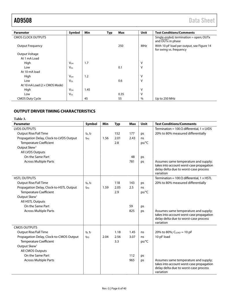
Parameter Symbol Min Typ Max Unit Test Conditions/Comments CMOS CLOCK OUTPUTS Single-ended; termination = open; OUTx
and OUTx in phase
Output Frequency 250 MHz With 10 pF load per output, see Figure 14 for swing vs. frequency
Output Voltage At 1 mA Load
High VOH 1.7 V Low VOL 0.1 V
At 10 mA load High VOH 1.2 V Low VOL 0.6 V
At 10 mA Load (2 × CMOS Mode) High VOH 1.45 V Low VOL 0.35 V
CMOS Duty Cycle 45 55 % Up to 250 MHz
OUTPUT DRIVER TIMING CHARACTERISTICS
Table 3. Parameter Symbol Min Typ Max Unit Test Conditions/Comments LVDS OUTPUTS Termination = 100 Ω differential, 1 × LVDS
Output Rise/Fall Time tR, tF 152 177 ps 20% to 80% measured differentially Propagation Delay, Clock-to-LVDS Output tPD 1.56 2.01 2.43 ns
Temperature Coefficient 2.8 ps/°C Output Skew1
All LVDS Outputs On the Same Part 48 ps Across Multiple Parts 781 ps Assumes same temperature and supply;
takes into account worst-case propagation delay delta due to worst-case process variation
HSTL OUTPUTS Termination = 100 Ω differential, 1 × HSTL Output Rise/Fall Time tR, tF 118 143 ps 20% to 80% measured differentially Propagation Delay, Clock-to-HSTL Output tPD 1.59 2.05 2.5 ns
Temperature Coefficient 2.9 ps/°C Output Skew1
All HSTL Outputs On the Same Part 59 ps Across Multiple Parts 825 ps Assumes same temperature and supply;
takes into account worst-case propagation delay delta due to worst-case process variation
CMOS OUTPUTS Output Rise/Fall Time tR, tF 1.18 1.45 ns 20% to 80%; CLOAD = 10 pF Propagation Delay, Clock-to-CMOS Output tPD 2.04 2.56 3.07 ns 10 pF load
Temperature Coefficient 3.3 ps/°C Output Skew1
All CMOS Outputs On the Same Part 112 ps Across Multiple Parts 965 ps Assumes same temperature and supply;
takes into account worst-case propagation delay delta due to worst-case process variation

Data Sheet AD9508
Rev. G | Page 7 of 40
Parameter Symbol Min Typ Max Unit Test Conditions/Comments OUTPUT LOGIC SKEW1 CMOS load = 10 pF and LVDS load = 100 Ω
LVDS Output(s) and HSTL Output(s) 77 119 ps Outputs on the same device; assumes worst-case output combination
LVDS Output(s) and CMOS Output(s) 497 700 ps Outputs on the same device; assumes worst-case output combination
HSTL Output(s) and CMOS Output(s) 424 622 ps Outputs on the same device; assumes worst-case output combination
1 Output skew is the difference between any two similar delay paths while operating at the same voltage and temperature.
LOGIC INPUTS
Table 4. Parameter Symbol Min Typ Max Unit Test Conditions/Comments
LOGIC INPUTS RESET, SYNC, IN_SEL
Input Voltage High VIH 1.7 V 2.5 V supply voltage operation
2.0 V 3.3 V supply voltage operation Low VIL 0.7 V 2.5 V supply voltage operation
0.8 V 3.3 V supply voltage operation Input Current IINH, IINL −300 +100 µA Input Capacitance CIN 2 pF
SERIAL PORT SPECIFICATIONS—SPI MODE
Table 5. Parameter Min Typ Max Unit Test Conditions/Comments CS SCLK has a 200 kΩ internal pull-down resistor
Input Voltage Logic 1 VDD − 0.4 V Logic 0 0.4 V
Input Current Logic 1 −4 µA Logic 0 −85 µA
Input Capacitance 2 µA SCLK
Input Voltage Logic 1 VDD − 0.4 V Logic 0 0.4 V
Input Current Logic 1 70 µA Logic 0 13 µA
Input Capacitance 2 pF SDIO
As Input Input Voltage
Logic 1 VDD − 0.4 V Logic 0 0.4 V
Input Current Logic 1 −1 µA Logic 0 −1 µA
Input Capacitance 2 pF
AD9508 Data Sheet
Rev. G | Page 8 of 40
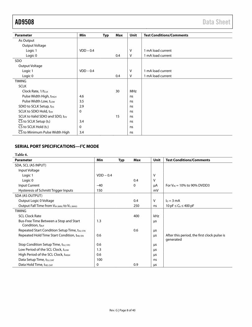
Parameter Min Typ Max Unit Test Conditions/Comments As Output
Output Voltage Logic 1 VDD − 0.4 V 1 mA load current Logic 0 0.4 V 1 mA load current
SDO Output Voltage
Logic 1 VDD − 0.4 V 1 mA load current Logic 0 0.4 V 1 mA load current
TIMING SCLK
Clock Rate, 1/tCLK 30 MHz Pulse Width High, tHIGH 4.6 ns Pulse Width Low, tLOW 3.5 ns
SDIO to SCLK Setup, tDS 2.9 ns SCLK to SDIO Hold, tDH 0 ns SCLK to Valid SDIO and SDO, tDV 15 ns CS to SCLK Setup (tS) 3.4 ns
CS to SCLK Hold (tC) 0 ns
CS to Minimum Pulse Width High 3.4 ns
SERIAL PORT SPECIFICATIONS—I2C MODE
Table 6. Parameter Min Typ Max Unit Test Conditions/Comments SDA, SCL (AS INPUT)
Input Voltage Logic 1 VDD − 0.4 V Logic 0 0.4 V
Input Current −40 0 µA For VIN = 10% to 90% DVDD3 Hysteresis of Schmitt Trigger Inputs 150 mV
SDA (AS OUTPUT) Output Logic 0 Voltage 0.4 V IO = 3 mA Output Fall Time from VIH (MIN) to VIL (MAX) 250 ns 10 pF ≤ Cb ≤ 400 pF
TIMING SCL Clock Rate 400 kHz Bus-Free Time Between a Stop and Start
Condition, tBUF 1.3 µs
Repeated Start Condition Setup Time, tSU; STA 0.6 µs Repeated Hold Time Start Condition, tHD; STA 0.6 µs After this period, the first clock pulse is
generated Stop Condition Setup Time, tSU; STO 0.6 µs Low Period of the SCL Clock, tLOW 1.3 µs High Period of the SCL Clock, tHIGH 0.6 µs Data Setup Time, tSU; DAT 100 ns Data Hold Time, tHD; DAT 0 0.9 µs

Data Sheet AD9508
Rev. G | Page 9 of 40
EXTERNAL RESISTOR VALUES FOR PIN STRAPPING MODE
Table 7. Parameter Resistor Polarity Min Typ Max Unit Test Conditions/Comments EXTERNAL RESISTORS Using 10% tolerance resistor
Voltage Level 0 Pull down to ground 820 Ω Voltage Level 1 Pull down to ground 1.8 kΩ Voltage Level 2 Pull down to ground 3.9 kΩ Voltage Level 3 Pull down to ground 8.2 kΩ Voltage Level 4 Pull up to VDD 820 Ω
Voltage Level 5 Pull up to VDD 1.8 kΩ Voltage Level 6 Pull up to VDD 3.9 kΩ Voltage Level 7 Pull up to VDD 8.2 kΩ
CLOCK OUTPUT ADDITIVE PHASE NOISE
Table 8. Parameter Min Typ Max Unit Test Conditions/Comments CLK-TO-HSTL OR LVDS ADDITIVE PHASE NOISE
CLK = 1474.56 MHz, OUTx = 1474.56 MHz Input slew rate > 1 V/ns Divide Ratio = 1
At 10 Hz Offset −88 dBc/Hz At 100 Hz Offset −100 dBc/Hz At 1 kHz Offset −109 dBc/Hz At 10 kHz Offset −116 dBc/Hz At 100 kHz Offset −135 dBc/Hz At 1 MHz Offset −144 dBc/Hz At 10 MHz Offset −148 dBc/Hz At 100 MHz Offset −149 dBc/Hz
CLK-TO-HSTL OR LVDS or CMOS ADDITIVE PHASE NOISE CLK = 625 MHz, OUTx = 125 MHz Input slew rate > 1 V/ns
Divide Ratio = 5 At 10 Hz Offset −114 dBc/Hz At 100 Hz Offset −125 dBc/Hz At 1 kHz Offset −133 dBc/Hz At 10 kHz Offset −141 dBc/Hz At 100 kHz Offset −159 dBc/Hz At 1 MHz Offset −162 dBc/Hz At 10 MHz Offset −163 dBc/Hz At 20 MHz Offset −163 dBc/Hz
CLK-TO-HSTL OR LVDS ADDITIVE PHASE NOISE CLK = 491.52 MHz, OUTx = 491.52 MHz Input slew rate > 1 V/ns
Divide Ratio = 1 At 10 Hz Offset −100 dBc/Hz At 100 Hz Offset −111 dBc/Hz At 1 kHz Offset −120 dBc/Hz At 10 kHz Offset −127 dBc/Hz At 100 kHz Offset −146 dBc/Hz At 1 MHz Offset −153 dBc/Hz At 10 MHz Offset −153 dBc/Hz At 20 MHz Offset −153 dBc/Hz

AD9508 Data Sheet
Rev. G | Page 10 of 40
CLOCK OUTPUT ADDITIVE TIME JITTER
Table 9. Parameter Min Typ Max Unit Test Conditions/Comments LVDS OUTPUT ADDITIVE TIME JITTER
CLK = 622.08 MHz, Outputs = 622.08 MHz 41 fs rms BW = 12 kHz to 20 MHz 70 fs rms BW = 20 kHz to 80 MHz 69 fs rms BW = 50 kHz to 80 MHz
CLK = 622.08 MHz, Outputs = 155.52 MHz 93 fs rms BW = 12 kHz to 20 MHz 144 fs rms BW = 20 kHz to 80 MHz 142 fs rms BW = 50 kHz to 80 MHz
CLK = 125 MHz, Outputs = 125 MHz 105 fs rms BW = 12 kHz to 20 MHz 209 fs rms BW = 20 kHz to 80 MHz 206 fs rms BW = 50 kHz to 80 MHz
CLK = 400 MHz, Outputs = 50 MHz 184 fs rms BW = 12 kHz to 20 MHz HSTL OUTPUT ADDITIVE TIME JITTER
CLK = 622.08 MHz, Outputs = 622.08 MHz 41 fs rms BW = 12 kHz to 20 MHz 56 fs rms BW = 100 Hz to 20 MHz
72 fs rms BW = 20 kHz to 80 MHz 70 fs rms BW = 50 kHz to 80 MHz
CLK = 622.08 MHz, Outputs = 155.52 MHz 76 fs rms BW = 12 kHz to 20 MHz 87 fs rms BW = 100 Hz to 20 MHz
158 fs rms BW = 20 kHz to 80 MHz 156 fs rms BW = 50 kHz to 80 MHz CMOS OUTPUT ADDITIVE TIME JITTER
CLK = 100 MHz, Outputs = 100 MHz 91 fs rms BW = 12 kHz to 20 MHz

Data Sheet AD9508
Rev. G | Page 11 of 40
ABSOLUTE MAXIMUM RATINGS Table 10. Parameter Rating Supply Voltage (VDD) 3.6 V Maximum Digital Input Voltage −0.5 V to VDD + 0.5 V CLK and CLK −0.5 V to VDD + 0.5 V
Maximum Digital Output Voltage −0.5 V to VDD + 0.5 V Storage Temperature Range −65°C to +150°C Operating Temperature Range −40°C to +85°C Lead Temperature (Soldering 10 sec) 300°C Junction Temperature 150°C
Stresses at or above those listed under Absolute Maximum Ratings may cause permanent damage to the product. This is a stress rating only; functional operation of the product at these or any other conditions above those indicated in the operational section of this specification is not implied. Operation beyond the maximum operating conditions for extended periods may affect product reliability.
The following equation determines the junction temperature on the application PCB:
TJ = TCASE + (ΨJT × PD)
where: TJ is the junction temperature (°C). TCASE is the case temperature (°C) measured by the customer at the top center of the package. ΨJT is the value as indicated in Table 11. PD is the power dissipation.
Values of θJA are provided for package comparison and PCB design considerations. θJA can be used for a first-order approxi-mation of TJ by the following equation:
TJ = TA + (θJA × PD)
where TA is the ambient temperature (°C).
Values of θJC are provided for package comparison and PCB design considerations when an external heat sink is required.
Values of θJB are provided for package comparison and PCB design considerations.
THERMAL CHARACTERISTICS Thermal characteristics established using JEDEC51-7 and JEDEC51-5 2S2P test boards.
Table 11. Thermal Characteristics, 24-Lead LFCSP
Symbol
Thermal Characteristic (JEDEC51-7 and JEDEC51-5 2S2P Test Boards1) Value2 Unit
θJA Junction-to-ambient thermal resistance per JEDEC JESD51-2 (still air)
43.5 °C/W
θJMA Junction-to-ambient thermal resistance, 1.0 m/sec airflow per JEDEC JESD51-6 (moving air)
40 °C/W
θJMA Junction-to-ambient thermal resistance, 2.5 m/sec airflow per JEDEC JESD51-6 (moving air)
38.5 °C/W
θJB Junction-to-board thermal resistance per JEDEC JESD51-8 (still air)
16.2 °C/W
θJC Junction-to-case thermal resistance (die-to-heat sink) per MIL-STD-883, Method 1012.1
7.1 °C/W
ΨJT Junction-to-top-of-package characterization parameter per JEDEC JESD51-2 (still air)
0.33 °C/W
1 The exposed pad on the bottom of the package must be soldered to ground (VSS) to achieve the specified thermal performance.
2 Results are from simulations. The PCB is a JEDEC multilayer type. Thermal performance for actual applications requires careful inspection of the conditions in the application to determine if they are similar to those assumed in these calculations.
ESD CAUTION

AD9508 Data Sheet
Rev. G | Page 12 of 40
PIN CONFIGURATION AND FUNCTION DESCRIPTIONS
Figure 2. Pin Configuration
Table 12. Pin Function Descriptions Pin No. Mnemonic Description 1 CS/S2 Chip Select/Pin Programming. Multipurpose pin. This pin is controlled by the PROG_SEL pin. Chip
Select (CS) is an active logic low CMOS input used in the SPI operation mode. When programming a device via SPI mode, CS must be held low. In systems where more than one AD9508 is present, this pin enables individual programming of each AD9508. In pin programming mode, this pin becomes S2. In this mode, S2 is hard wired with a resistor to either VDD or ground. The resistor value and resistor biasing determine the output divider value for the outputs on Pin 11 and Pin 12. See the Pin Strapping to Program on Power-Up section for more details.
2 OUT0 LVDS/HSTL Differential Output or Single-Ended CMOS Output. 3 OUT0 Complementary LVDS/HSTL Differential Output or Single-Ended CMOS Output.
4 SDO/S3 Serial Data Output/Pin Programming. Multipurpose pin. This pin is controlled by the PROG_SEL pin. SDO is configured as an output to read back the internal register settings in SPI mode operation. In pin programming mode, this pin becomes S3, which is hard wired with a resistor to either VDD or ground. The resistor value and resistor biasing determine the output divider value for the outputs on Pin 16 and Pin 17. See the Pin Strapping to Program on Power-Up section for more details.
5 EXT_CAP0 Node for External Decoupling Capacitor for LDO. Tie this pin to a 0.47 µF capacitor to ground. 6 VDD Power Supply (2.5 V or 3.3 V Operation). 7 OUT1 LVDS/HSTL Differential Output or Single-Ended CMOS Output. 8 OUT1 Complementary LVDS/HSTL Differential Output or Single-Ended CMOS Output.
9 S4 Pin Programming. Use this pin in pin programming mode only. The PROG_SEL pin determines which programming mode is used. In pin programming mode, S4 is hardwired with a resistor to either VDD or ground. The resistor value and resistor biasing determine the output logic levels used for the outputs on Pin 2, Pin 3, Pin 7, and Pin 8. See the Pin Strapping to Program on Power-Up section for more details.
10 S5 Pin Programming. Use this pin in pin programming mode only. The PROG_SEL pin determines which programming mode is used. In pin programming mode, S5 is hardwired with a resistor to either VDD or ground. The resistor value and resistor biasing determine the output logic levels used for the outputs on Pin 11, Pin 12, Pin 16, and Pin 17. See the Pin Strapping to Program on Power-Up section for more details.
11 OUT2 LVDS/HSTL Differential Output or Single-Ended CMOS Output. 12 OUT2 Complementary LVDS/HSTL Differential Output or Single-Ended CMOS Output.
13 VDD Power Supply (2.5 V or 3.3 V Operation). 14 EXT_CAP1 Node for External Decoupling Capacitor for LDO. Tie this pin to a 0.47 µF capacitor to ground. 15 PROG_SEL Three-State CMOS Input. Pin 15 selects the type of device programming interface to be used (SPI, I2C,
or pin programming). 16 OUT3 LVDS/HSTL Differential Output or Single-Ended CMOS Output. 17 OUT3 Complementary LVDS/HSTL Differential Output or Single-Ended CMOS Output.
21
3456
181716151413VDD
EXT_CAP0SDO/S3
OUT0OUT0CS/S2
VDD
NOTES1. THE EXPOSED DIE PAD MUST BE CONNECTED TO GROUND (VSS).
EXT_CAP1PROG_SELOUT3OUT3RESET
8 9 10 117O
UT1 S4 S5
OU
T212
OU
T2
OU
T1
20 1921SY
NC
SCLK
/SC
L/S0
CLK
22C
LK23
IN_S
EL24
SDIO
/SD
A/S
1
AD9508TOP VIEW
1116
1-00
2

Data Sheet AD9508
Rev. G | Page 13 of 40
Pin No. Mnemonic Description 18 RESET CMOS Input. Device Reset. When this active low pin is asserted, the internal register settings enter their
default state after the RESET is released. Note that RESET also serves as a power-down of the device while an active low signal is applied to the pin. The RESET pin has an internal 24 kΩ pull-up resistor.
19 SCLK/SCL/S0 Serial Programming Clock/Data Clock/Programming Pin. Multipurpose pin controlled by the PROG_SEL pin used for serial programming clock (SCLK) in SPI mode or data clock (SCL) for serial programming in I2C Mode. The PROG_SEL pin determines which programming mode is used. In pin programming mode, this pin becomes S0. In this mode, S0 is hardwired with a resistor to either VDD or ground. The resistor value and resistor biasing determine the output divider values for the outputs on Pin 2 and Pin 3. See the Pin Strapping to Program on Power-Up section for more details.
20 SYNC Clock Synchronization. When this pin is active low, the output drivers are held static and then synchronized on a low-to-high transition of this pin. The SYNC pin has an internal 24 kΩ pull-up resistor.
21 CLK Differential Clock Input or Single-Ended CMOS Input. Whether this pin serves as the differential clock input or the single-ended CMOS input depends on the logic state of the IN_SEL pin.
22 CLK Complementary Differential Clock Input.
23 IN_SEL CMOS Input. A logic high configures the CLK and CLK inputs for a differential input signal. A logic low configures the input for single-ended CMOS applied to the CLK pin. AC-couple the unused CLK to ground with a 0.1 µF capacitor.
24 SDIO/SDA/S1 Serial Data Input and Output (SPI)/Serial Data (I2C)/Pin Programming. Pin 24 is a multipurpose input controlled by the PROG_SEL pin used for SPI (SDIO), I2C (SDA), and pin strapping modes (S1). When the device is in 4-wire SPI mode, data is written via SDIO. In 3-wire mode, both data reads and writes occur on this pin. There is no internal pull-up/pull-down resistor on this pin. In I2C mode, SDA serves as the serial data pin. The PROG_SEL pin determines which programming mode is used. In pin programming mode, this pin becomes S1. In this mode, S1 is hardwired with a resistor to either VDD or ground. The resistor value and resistor biasing determine the output divider values for the outputs on Pin 7 and Pin 8. See the Pin Strapping to Program on Power-Up section for more details.
EP Exposed Pad. The exposed die pad must be connected to ground (VSS).

AD9508 Data Sheet
Rev. G | Page 14 of 40
TYPICAL PERFORMANCE CHARACTERISTICS
Figure 3. LVDS Differential Output Waveform at 800 MHz
Figure 4. LVDS Differential Output Waveform at 156.25 MHz
Figure 5. Power Supply Current vs. Input Frequency and Number of Outputs Used, LVDS
Figure 6. LVDS Differential Output Swing vs. Frequency
Figure 7. LVDS Differential Output Swing vs. Power Supply Voltage
Figure 8. LVDS Propagation Delay vs. Input Differential Voltage
TIME (250ps/DIV)
VO
LT
AG
E (
100
mV
/DIV
)
1116
1-00
3
TIME (1.5ns/DIV)
VO
LT
AG
E (
100m
V/D
IV)
1116
1-00
4
200ONE OUTPUT (mA)TWO OUTPUTS (mA)THREE OUTPUTS (mA)FOUR OUTPUTS (mA)
150
100
0
50
CU
RR
EN
T (
mA
)
FREQUENCY (MHz)
0 400 800 1200 1600
1116
1-00
5
800
FREQUENCY (MHz)
100 300 900700500 1100 1300 1500
DIF
FE
RE
NT
IAL
OU
TP
UT
SW
ING
(m
V p
-p)
700
600
500
400
1116
1-00
6
800
POWER SUPPLY (V)
2.3 2.5 3.12.92.7 3.3 3.5
DIF
FE
RE
NT
IAL
OU
TP
UT
SW
ING
(m
V p
-p)
780
760
740
720
700
1116
1-00
8
2.0
2.1
2.2
2.3
2.4
1.8
1.72.01.6 1.81.41.21.00.80.60.40.2
1.9
PR
OP
AG
AT
ION
DE
LA
Y (
ns)
INPUT DIFFERENTIAL (V p-p) 1116
1-00
9
Data Sheet AD9508
Rev. G | Page 15 of 40
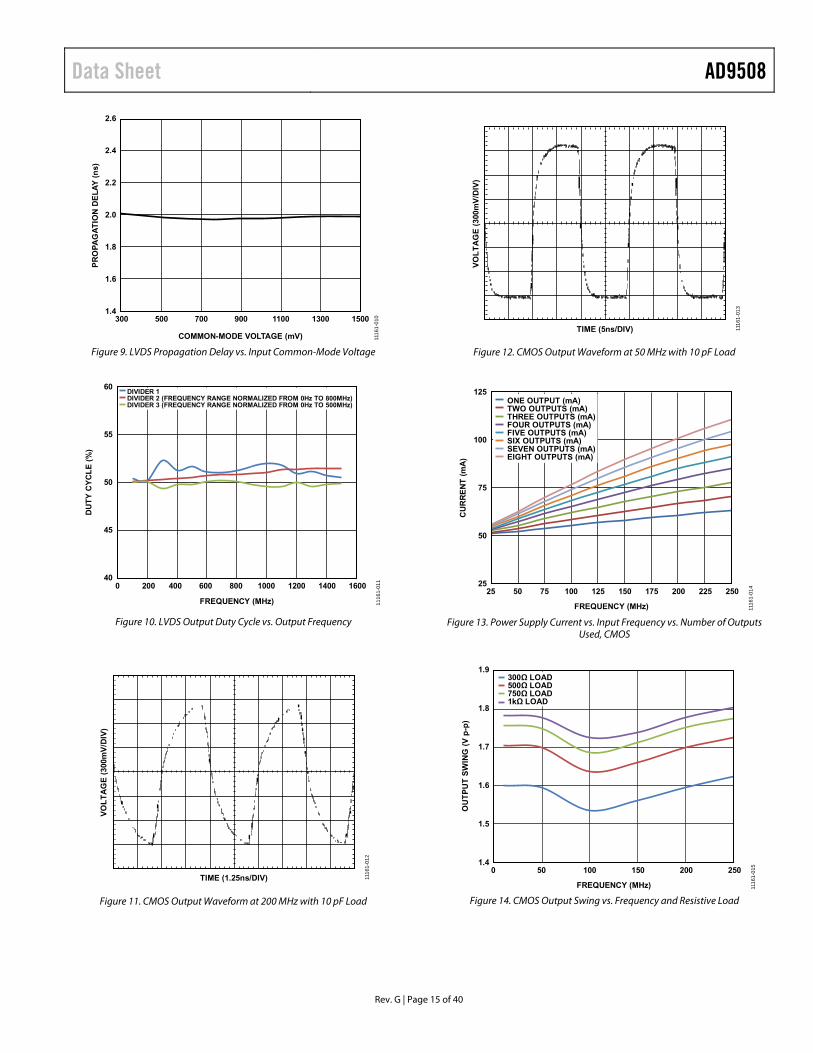
Figure 9. LVDS Propagation Delay vs. Input Common-Mode Voltage
Figure 10. LVDS Output Duty Cycle vs. Output Frequency
Figure 11. CMOS Output Waveform at 200 MHz with 10 pF Load
Figure 12. CMOS Output Waveform at 50 MHz with 10 pF Load
Figure 13. Power Supply Current vs. Input Frequency vs. Number of Outputs Used, CMOS
Figure 14. CMOS Output Swing vs. Frequency and Resistive Load
COMMON-MODE VOLTAGE (mV)
PR
OP
AG
AT
ION
DE
LA
Y (
ns)
2.0
1.8
1.6
1.4
2.6
2.4
2.2
300 500 700 900 1100 1300 1500
1116
1-01
0
55
FREQUENCY (MHz)
4002000 600 800 1000 1200 1400 1600
DU
TY
CY
CL
E (
%)
60
50
45
40
DIVIDER 1DIVIDER 2 (FREQUENCY RANGE NORMALIZED FROM 0Hz TO 800MHz)DIVIDER 3 (FREQUENCY RANGE NORMALIZED FROM 0Hz TO 500MHz)
1116
1-01
1
TIME (1.25ns/DIV)
VO
LT
AG
E (
300m
V/D
IV)
1116
1-01
2
TIME (5ns/DIV)
VO
LT
AG
E (
300m
V/D
IV)
1116
1-01
3
CU
RR
EN
T (
mA
)
25 50 75 100 12525
50
75
100
125
150 175 200 225 250
FREQUENCY (MHz)
ONE OUTPUT (mA)TWO OUTPUTS (mA)THREE OUTPUTS (mA)FOUR OUTPUTS (mA)FIVE OUTPUTS (mA)SIX OUTPUTS (mA)SEVEN OUTPUTS (mA)EIGHT OUTPUTS (mA)
1116
1-01
4
01.4
1.5
1.6
1.7
1.8
1.9
50 100 150 200 250
OU
TP
UT
SW
ING
(V
p-p
)
FREQUENCY (MHz)
300Ω LOAD500Ω LOAD750Ω LOAD1kΩ LOAD
1116
1-01
5

AD9508 Data Sheet
Rev. G | Page 16 of 40
Figure 15. CMOS Output Swing vs. Frequency and Temperature (10 pF Load)
Figure 16. CMOS Output Swing vs. Frequency and Capacitive Load (2 pF, 5 pF, 10 pF, 20 pF)
Figure 17. HSTL Differential Output Waveform at 800 MHz
Figure 18. HSTL Differential Output Waveform at 156.25 MHz
Figure 19. Power Supply Current vs. Input Frequency and Number of Outputs Used, HSTL
Figure 20. HSTL Differential Output Swing vs. Frequency
01.0
1.4
1.2
1.6
1.8
2.0
50 100 150 200 250
OU
TPU
T SW
ING
(V p
-p)
FREQUENCY (MHz) 1116
1-01
6
–40°C+25°C+85°C
01.1
1.3
1.5
1.7
1.9
50 100 150 200 250
FREQUENCY (MHz)
OU
TPU
T SW
ING
(V p
-p)
2pF LOAD5pF LOAD10pF LOAD20pF LOAD
1116
1-01
7
TIME (250ps/DIV)
VOLT
AG
E (3
00m
V/D
IV)
1116
1-01
8
TIME (1.5ns/DIV)
VOLT
AG
E (3
00m
V/D
IV)
1116
1-01
9
200
150
100
0
50
CU
RR
ENT
(mA
)
FREQUENCY (MHz)
0 400 800 1200 1600
ONE OUTPUT (mA)TWO OUTPUTS (mA)THREE OUTPUTS (mA)FOUR OUTPUTS (mA)
1116
1-02
0
2.0
1.8
FREQUENCY (MHz)
100 300 900700500 1100 1300 1500
DIF
FER
ENTI
AL O
UTP
UT
SWIN
G (m
V p-
p) 1.9
1.7
1.6
1.5
1.4
1.3
1.2
1116
1-00
7

Data Sheet AD9508
Rev. G | Page 17 of 40
Figure 21. HSTL Differential Output Swing vs. Power Supply Voltage
Figure 22. HSTL Propagation Delay vs. Input Differential Voltage
Figure 23. HSTL Propagation Delay vs. Input Common-Mode Voltage
Figure 24. HSTL Output Duty Cycle vs. Output Frequency
Figure 25. Additive Broadband Jitter vs. Input Slew Rate, LVDS, HSTL (Calculated from SNR of ADC Method)
Figure 26. Absolute Phase Noise in HSTL Mode with Clock Input at 622.08 MHz and Outputs = 622.08 MHz, 311.04 MHz, 155.52 MHz
2.0
POWER SUPPLY (V)
2.3 2.5 3.12.92.7 3.3 3.5
DIF
FE
RE
NT
IAL
OU
TP
UT
SW
ING
(m
V p
-p)
1.9
1.8
1.7
1.6
1.5
1116
1-02
111
161-
022
2.0
2.1
2.2
2.3
2.4
1.8
1.72.01.6 1.81.41.21.00.80.60.40.2
1.9
PR
OP
AG
AT
ION
DE
LA
Y (
ns)
INPUT DIFFERENTIAL (V p-p)
COMMON-MODE VOLTAGE (mV)
PR
OP
AG
AT
ION
DE
LA
Y (
ns)
2.0
1.8
1.6
1.4
2.6
2.4
2.2
300 500 700 900 1100 1300 1500
1116
1-02
3
55
FREQUENCY (MHz)
4002000 600 800 1000 1200 1400 1600
DU
TY
CY
CL
E (
%)
60
50
45
40
1116
1-02
4
DIVIDER 1DIVIDER 2 (FREQUENCY RANGE NORMALIZED FROM 0Hz TO 800MHz)DIVIDER 3 (FREQUENCY RANGE NORMALIZED FROM 0Hz TO 500MHz)
80
90
100
110
120
130
140
150
0 2 4 6 8 10
JIT
TE
R (
fsrm
s)
SLEW RATE (V/ns) 1116
1-22
7
–170
–160
–150
–140
–130
–120
–110
–100
–90
–80
10 100 1k 10k 100k 10M 100M1M
PH
AS
E N
OIS
E (
dB
c/H
z)
FREQUENCY OFFSET (Hz)
HSTL 155.52MHzHSTL 311.04MHzHSTL 622.08MHz
1116
1-22
8

AD9508 Data Sheet
Rev. G | Page 18 of 40
Figure 27. Absolute Phase Noise in LVDS Mode with Clock Input at 622.08 MHz and Outputs = 622.08 MHz, 311.04 MHz, 155.52 MHz
Figure 28. Absolute Phase Noise of Clock Source at 622.08 MHz
Figure 29. Additive Phase Noise with Clock Input = 1474.56 MHz with HSTL Outputs = 1474.76 MHz
Figure 30. Additive Phase Noise with Clock Input = 1500 MHz with HSTL
Outputs = 100 MHz
Figure 31. Additive Phase Noise with Clock Input = 622.08 MHz with HSTL
Outputs = 155.52 MHz
Figure 32. Additive Phase Noise with Clock Input = 622.08 MHz with LVDS Outputs = 622.08 MHz
–160
–150
–140
–130
–120
–110
–100
–90
–80
PHA
SE N
OIS
E (d
Bc/
Hz)
LVDS 155.52MHzLVDS 311.04MHzLVDS 622.08MHz
1116
1-22
9
10 100 1k 10k 100k 10M 100M1M
FREQUENCY OFFSET (Hz)
–170
–160
–150
–140
–130
–120
–110
–100
–90
–80
1 1000 100000 10000000
PHA
SE N
OIS
E (d
Bc/
Hz)
FREQUENCY OFFSET (MHz) 1116
1-23
0
–170
–160
–150
–140
–130
–120
–110
–100
–90
–80
PHA
SE N
OIS
E (d
Bc/
Hz)
1116
1-32
9
10 100 1k 10k 100k 10M 100M1M
FREQUENCY (Hz)
MARKERFREQUENCY1. 10Hz2. 100Hz3. 1kHz4. 10kHz5. 100kHz6. 1MHz7. 10MHz8. 100MHz
AMPLITUDE–89.57dBc/Hz–100.45dBc/Hz–109.97dBc/Hz–116.93dBc/Hz–135.33dBc/Hz–144.39dBc/Hz–148.66dBc/Hz–149.78dBc/Hz
2
3
4
5
6 78
1
–80
–90
–100
–110
–120
–130
–140
–150
–160
–17010 100 1k 10k 100k 1M 10M 100M
MARKERFREQUENCY1. 10Hz2. 100Hz3. 1kHz4. 10kHz5. 100.5kHz6. 1MHz7. 10MHz
AMPLITUDE–116.04dBc/Hz–126.68dBc/Hz–135.27dBc/Hz–142.56dBc/Hz–159.42dBc/Hz–161.97dBc/Hz–164.55dBc/Hz
2
3
4
5 67
1
FREQUENCY (Hz)
PHA
SE N
OIS
E (d
Bc/
Hz)
1116
1-33
0
–80
–90
–100
–110
–120
–130
–140
–150
–160
–17010 100 1k 10k 100k 1M 10M 100M
MARKERFREQUENCY1. 10Hz2. 100Hz3. 1kHz4. 10kHz5. 100.5kHz6. 1MHz7. 10MHz8. 20MHz
AMPLITUDE–112.35dBc/Hz–118.81dBc/Hz–127.84dBc/Hz–135.97dBc/Hz–151.91dBc/Hz–157.87dBc/Hz–159.78dBc/Hz–157.88dBc/Hz
FREQUENCY (Hz)
PHA
SE N
OIS
E (d
Bc/
Hz)
1116
1-12
9
2
3
4
56 7 8
1
–80
–90
–100
–110
–120
–130
–140
–150
–160
–17010 100 1k 10k 100k 1M 10M 100M
MARKERFREQUENCY1. 10Hz2. 100Hz3. 1kHz4. 10kHz5. 100.5kHz6. 1MHz7. 10MHz8. 20MHz
AMPLITUDE–100.17dBc/Hz–109.18dBc/Hz–117.67dBc/Hz–124.94dBc/Hz–143.83dBc/Hz–151.64dBc/Hz–153.81dBc/Hz–152.87dBc/Hz
2
3
4
5
6 7 8
1
FREQUENCY (Hz)
PHA
SE N
OIS
E (d
Bc/
Hz)
1116
1-13
0

Data Sheet AD9508
Rev. G | Page 19 of 40
Figure 33. Additive Phase Noise with Clock Input = 100 MHz with CMOS
Outputs = 100 MHz
–80
–90
–100
–110
–120
–130
–140
–150
–160
–17010 100 1k 10k 100k 1M 10M 100M
MARKERFREQUENCY1. 10Hz2. 100Hz3. 1kHz4. 10kHz5. 100.5kHz6. 1MHz7. 10MHz8. 20MHz
AMPLITUDE–114.15dBc/Hz–127.18dBc/Hz–134.13dBc/Hz–141.63dBc/Hz–154.66dBc/Hz–155.37dBc/Hz–152.86dBc/Hz–153.09dBc/Hz
2
1
3
4
5 6 7 8
FREQUENCY (Hz)
PHA
SE N
OIS
E (d
Bc/
Hz)
1116
1-13
1

AD9508 Data Sheet
Rev. G | Page 20 of 40
TEST CIRCUITS INPUT/OUTPUT TERMINATION RECOMMENDATIONS
Figure 34. Typical AC-Coupled or DC-Coupled LVDS or HSTL Configurations
Figure 35. Typical AC-Coupled or DC-Coupled CML Configurations
Figure 36. Typical AC-Coupled or DC-Coupled LVPECL Configurations
Figure 37. Typical 2.5 V or 3.3 V CMOS Configurations for Short Trace Lengths
Figure 38. 1.8 V CMOS Logic Configuration for Input Clock Using Differential Mode
Figure 39. AC-Coupled LVDS or HSTL Output Driver (100 Ω Resistor Can Go on Either Side of Decoupling Capacitors Placed As Close As Possible To The
Destination Receiver)
Figure 40. DC-Coupled LVDS or HSTL Output Driver
Figure 41. Interfacing the HSTL Driver to a 3.3 V LVPECL Input (This Method Incorporates Impedance Matching and DC Biasing for Bipolar LVPECL
Receivers. If the Receiver Is Self-Biased, the Termination Scheme Shown in Figure 39 Is Recommended.)
100Ω
CLK
CLK
100Ω
CLK
CLK11
161-
132
AD9508
AD9508
CLK
CLK
CLK
CLK
VCC
VCC
1116
1-13
3
AD9508
AD9508
CLK
CLK
50Ω 50Ω
VCC – 2V
CLK
CLK
50Ω 50Ω
AD9508
AD9508
VCC – 2V
1116
1-13
4
CLK
CLK
AD9508
1116
1-13
5
0.1µF
LOGIC 1
0.1µF
1.8V CMOS DRIVERIN_SEL
CLK
CLK
AD9508
1116
1-20
011
161-
136
DOWNSTREAMDEVICE
WITH HIGHIMPEDANCEINPUT ANDINTERNALDC-BIAS
0.1µF
0.1µF
100ΩAD9508HSTL ORLVDS
1116
1-13
7
AD9508HSTL ORLVDS
Z0 = 50Ω
Z0 = 50Ω
SINGLE-ENDED(NOT COUPLED)
LVDS OR 1.8V HSTLHIGH-IMPEDANCE
DIFFERENTIALRECEIVER
100Ω
1116
1-13
8
3.3VLVPECL
0.1µF
0.1µF
AD95081.8VHSTL
Z0 = 50Ω
Z0 = 50Ω
SINGLE-ENDED(NOT COUPLED)
82Ω
VS = 3.3V
82Ω
127Ω127Ω

Data Sheet AD9508
Rev. G | Page 21 of 40
TERMINOLOGY Phase Jitter and Phase Noise An ideal sine wave can be thought of as having a continuous and an even progression phase with time from 0 degrees to 360 degrees for each cycle. Actual signals, however, display a certain amount of variation from ideal phase progression over time. This phenomenon is phase jitter. Although many causes can contribute to phase jitter, one major cause is random noise, characterized statistically as being Gaussian (normal) in distribution.
Phase jitter leads to a spreading out of the energy of the sine wave in the frequency domain, producing a continuous power spectrum. This power spectrum is usually reported as a series of values whose units are dBc/Hz at a given offset in frequency from the sine wave (carrier). The value is a ratio (expressed in dB) of the power contained within a 1 Hz bandwidth with respect to the power at the carrier frequency. For each measurement, the offset from the carrier frequency is also given.
It is meaningful to integrate the total power contained within some interval of offset frequencies (for example, 10 kHz to 10 MHz). This is called the integrated phase noise over that frequency offset interval and can be readily related to the time jitter due to the phase noise contained within that offset frequency interval.
Phase noise has a detrimental effect on the performance of ADCs, DACs, and RF mixers. It lowers the achievable dynamic range of the converters and mixers, although they are affected in somewhat different ways.
Time Jitter Phase noise is a frequency domain phenomenon. In the time domain, the same effect is exhibited as with time jitter. When observing a sine wave, the time of successive zero crossings varies.
In a square wave, the time jitter is a displacement of the edges from their ideal (regular) times of occurrence. In both cases, the variations in timing from the ideal are the time jitter. Because these variations are random in nature, the time jitter is specified in units of seconds root mean square (rms) or one sigma of the Gaussian distribution.
Time jitter that occurs on a sampling clock for a DAC or an ADC decreases the SNR and dynamic range of the converter. A sampling clock with the lowest possible jitter provides the highest performance from a given converter.
Additive Phase Noise Additive phase noise is the amount of phase noise that is attributable only to the device or subsystem being measured. The residual phase noise system makes use of two devices operating in perfect quadrature. The correlated noise of any external components common to both devices (such as clock sources) is not present. This makes it possible to predict the degree to which the device is going to affect the total system phase noise when used in conjunction with the various oscillators and clock sources, each of which contribute their own phase noise to the total. In many cases, the phase noise of one element dominates the system phase noise.
Additive Time Jitter Additive time jitter refers to the amount of time jitter that is attributable to the device or subsystem being measured. It is calculated by integrating the additive phase noise over a specific range. This makes it possible to predict the degree to which the device is going to impact the total system time jitter when used in conjunction with the various oscillators and clock sources, each of which contribute their own time jitter to the total. In many cases, the time jitter of the external oscillators and clock sources dominates the system time jitter.

AD9508 Data Sheet
Rev. G | Page 22 of 40
THEORY OF OPERATION DETAILED BLOCK DIAGRAM
Figure 42. Detailed Block Diagram
The AD9508 accepts either a differential input clock applied to the CLK and CLK pins or a single-ended 1.8 V (if ac-coupled) 2.5 V or 3.3 V CMOS clock applied to the CLK pin. The input clock signal is sent to the clock distribution section, which has programmable dividers and phase offset adjustment. The clock distribution section operates at speeds of up to 1650 MHz.
The divider range under SPI or I2C control ranges from 1 to divide-by-1024 and the phase offset adjustment is equipped with 11 bits of resolution. However, in pin programming mode, the divider range is limited to a maximum divide-by-16 and there is no phase offset adjustment available.
The outputs can be configured to as many as four LVDS/HSTL differential outputs or as many as eight 1.8 V CMOS single-ended outputs. In addition, the output current for the different outputs is adjustable for output drive strength.
The device can be powered with either a 3.3 V or 2.5 V external supply; however, the internal supply on the chip runs off an internal 1.8 V LDO, delivering high performance with minimal power consumption.
PROGRAMMING MODE SELECTION The AD9508 supports both SPI and I2C protocols, and a pin strapping option to program the device. The active interface depends on the logic state of the PROG_SEL pin. See Table 13 for programming mode selections. See the Serial Control Port and Pin Strapping to Program on Power-Up sections for more detailed information.
Table 13. SPI/I2C/Pin Serial Port Setup PROG_SEL SPI/I2C/Pin Float SPI Logic 0 I2C Logic 1 Pin programming control
DIGITAL LOGICAND
REGISTERS
SPIINTERFACE
I2CINTERFACE
10-BITDIVIDER
SCL
SDA
CLK
SPI/I2C/PIN_PROG
COARSEA/D
PIN PROGRAMREAD CONTROL
SYNC
LVDS/HSTL/CMOSOUTPUTS
LDO
SUB LDO
SUB LDO
VDD
RESET
LDO
REVISION ID
11-BIT∆Φ
11-BIT∆Φ
11-BIT∆Φ
11-BIT∆Φ
10-BITDIVIDER
10-BITDIVIDER
10-BITDIVIDER
CLK
IN_SEL
PROG_SEL
SCLK/SCL/S0
SDIO/SDA/S1
SDO/S3
S4
S5
CS/S2
EXT_CAP0
OUT0
OUT0
OUT1
OUT1
OUT2
OUT2
OUT3
OUT3
EXT_CAP1
VDD
1116
1-13
9
6

Data Sheet AD9508
Rev. G | Page 23 of 40
CLOCK INPUT The IN_SEL pin controls the desired input clock configuration. When the IN_SEL pin is set for single-ended operation, the device expects 1.8 V (if ac-coupled), 2.5 V, or 3.3 V CMOS-compatible logic levels on the CLK input pin. Bypass the unused CLK pin to ground with a 0.1 µF capacitor.
Note that if 2.5 V CMOS logic is used for single-ended input clock mode, the 2.5 V power supply option is recommended instead of 3.3 V operation to avoid possible duty cycle distortion. Duty cycle distortion can occur when the switching threshold level (VDD/2 or 1.65 V for 3.3 V operation) is increased and slow rise and falls times exist at the clock input.
1.8 V CMOS logic levels are not recommended in a single-ended CMOS configuration due to VIH being too close to the input threshold voltage. However, the differential input clock mode can be used for a 1.8 V CMOS input, and Figure 38 shows the recommended configuration for a 1.8 V CMOS input clock.
When the IN_SEL pin is set for differential input clock mode, the inputs of the AD9508 are internally self biased. The internal inputs have a resistor divider, which sets the common-mode level. The complementary input is biased about 30 mV lower than the true input to avoid oscillations in the event that the input signal ceases. See Figure 43 for the equivalent differential input circuit.
Figure 43. AD9508 Differential Input Stage
The inputs can be ac-coupled or dc-coupled in differential mode. See Table 14 for input logic compatibility. The user can supply a single-ended input with the input in differential mode by ac or dc coupling to one side of the differential input and bypassing the other input to ground by a capacitor.
Note that jitter performance degrades with low input slew rate, as shown in Figure 25. See Figure 34 through Figure 37 for different input clock termination schemes.
Table 14. CLK and CLK Differential Input Logic Compatibility Input Logic Type Input Common Mode (V) Input Voltage Swing (per leg) (V) AC-Coupled DC-Coupled 3.3 V CML 2.9 0.8 Yes Not allowed 2.5 V CML 2.1 0.8 Yes Not allowed 1.8 V CML 1.4 0.8 Yes Yes 3.3 V CMOS1 1.65 3.3 Not allowed Yes 2.5 V CMOS1, 2 1.25 2.5 Not allowed Yes 1.8 V CMOS3 0.9 1.8 Yes Not recommended 1.5 V HSTL 0.75 0.75 Yes Yes LVDS 1.25 0.4 Yes Yes 3.3 V LVPECL 2.0 0.8 Yes Not allowed 2.5 V LVPECL 1.2 0.8 Yes Yes 1 IN_SEL is set for single-ended CMOS mode. 2 VDD = 2.5 V operation recommended vs. VDD = 3.3 V operation. 3 Refer to Figure 38 for configuration.
12.5kΩ 13kΩ
16.5kΩ 16kΩ
VDD
CLKCLK
GND 1116
1-14
0
AD9508 Data Sheet
Rev. G | Page 24 of 40
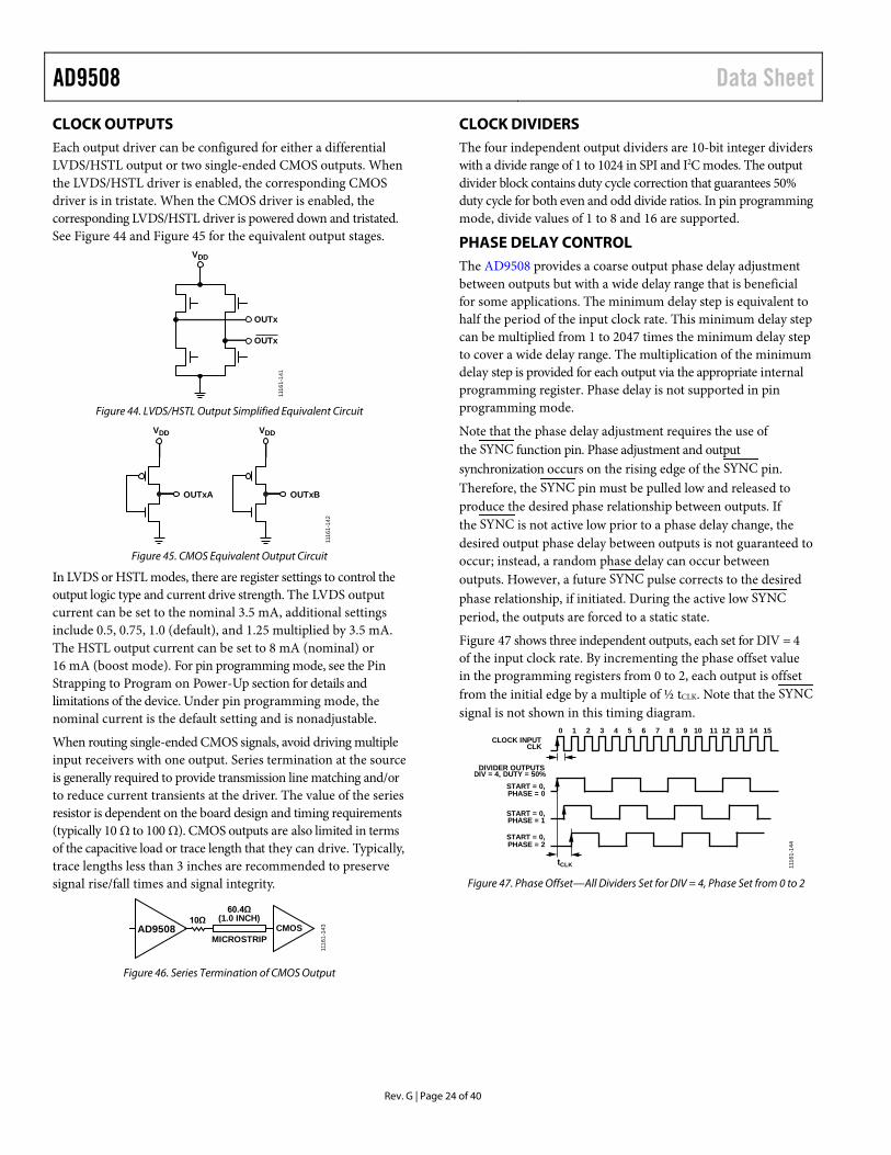
CLOCK OUTPUTS Each output driver can be configured for either a differential LVDS/HSTL output or two single-ended CMOS outputs. When the LVDS/HSTL driver is enabled, the corresponding CMOS driver is in tristate. When the CMOS driver is enabled, the corresponding LVDS/HSTL driver is powered down and tristated. See Figure 44 and Figure 45 for the equivalent output stages.
Figure 44. LVDS/HSTL Output Simplified Equivalent Circuit
Figure 45. CMOS Equivalent Output Circuit
In LVDS or HSTL modes, there are register settings to control the output logic type and current drive strength. The LVDS output current can be set to the nominal 3.5 mA, additional settings include 0.5, 0.75, 1.0 (default), and 1.25 multiplied by 3.5 mA. The HSTL output current can be set to 8 mA (nominal) or 16 mA (boost mode). For pin programming mode, see the Pin Strapping to Program on Power-Up section for details and limitations of the device. Under pin programming mode, the nominal current is the default setting and is nonadjustable.
When routing single-ended CMOS signals, avoid driving multiple input receivers with one output. Series termination at the source is generally required to provide transmission line matching and/or to reduce current transients at the driver. The value of the series resistor is dependent on the board design and timing requirements (typically 10 Ω to 100 Ω). CMOS outputs are also limited in terms of the capacitive load or trace length that they can drive. Typically, trace lengths less than 3 inches are recommended to preserve signal rise/fall times and signal integrity.
Figure 46. Series Termination of CMOS Output
CLOCK DIVIDERS The four independent output dividers are 10-bit integer dividers with a divide range of 1 to 1024 in SPI and I2C modes. The output divider block contains duty cycle correction that guarantees 50% duty cycle for both even and odd divide ratios. In pin programming mode, divide values of 1 to 8 and 16 are supported.
PHASE DELAY CONTROL The AD9508 provides a coarse output phase delay adjustment between outputs but with a wide delay range that is beneficial for some applications. The minimum delay step is equivalent to half the period of the input clock rate. This minimum delay step can be multiplied from 1 to 2047 times the minimum delay step to cover a wide delay range. The multiplication of the minimum delay step is provided for each output via the appropriate internal programming register. Phase delay is not supported in pin programming mode.
Note that the phase delay adjustment requires the use of the SYNC function pin. Phase adjustment and output synchronization occurs on the rising edge of the SYNC pin. Therefore, the SYNC pin must be pulled low and released to produce the desired phase relationship between outputs. If the SYNC is not active low prior to a phase delay change, the desired output phase delay between outputs is not guaranteed to occur; instead, a random phase delay can occur between outputs. However, a future SYNC pulse corrects to the desired phase relationship, if initiated. During the active low SYNC period, the outputs are forced to a static state.
Figure 47 shows three independent outputs, each set for DIV = 4 of the input clock rate. By incrementing the phase offset value in the programming registers from 0 to 2, each output is offset from the initial edge by a multiple of ½ tCLK. Note that the SYNC signal is not shown in this timing diagram.
Figure 47. Phase Offset—All Dividers Set for DIV = 4, Phase Set from 0 to 2
OUTx
OUTx
VDD
1116
1-14
1
OUTxA OUTxB
1116
1-14
2
VDDVDD
AD9508 CMOS10Ω
60.4Ω(1.0 INCH)
MICROSTRIP
1116
1-14
3
1 2 3 4 5 6 7 8 9 10 11 12 13 14 150CLOCK INPUT
CLK
DIVIDER OUTPUTSDIV = 4, DUTY = 50%
START = 0,PHASE = 0
START = 0,PHASE = 1
START = 0,PHASE = 2
tCLK 1116
1-14
4

Data Sheet AD9508
Rev. G | Page 25 of 40
RESET MODES The AD9508 has a power-on reset (POR) and other ways to apply a reset condition to the chip.
Power-On Reset
During chip power-up, an internal power-on reset pulse is issued when VDD reaches ~1.15 V and restores the chip to the default on-chip setting. It takes ~20 ms for the outputs to begin toggling after the power-on reset pulse signal is internally generated.
In SPI or I2C modes, the default power-on state of the AD9508 is configured as a buffer with the dividers set to divide by 1. In pin programmable mode, the part is configured per the hardwiring of the S0 to S5 pins.
Hardware Reset via the RESET Pin
A hard asynchronous reset is executed by briefly pulling RESET low. This restores the chip to the on-chip default register settings. It takes ~20 ms for the outputs to begin toggling after RESET is released.
Soft Reset via the Serial Port
A soft reset is initiated by setting Bit 2 and Bit 5 in Register 0x000. Except for Register 0x000, when Bit 5 and Bit 2 are set, the chip enters a soft reset mode and restores the chip to the on-chip setting. These bits are self clearing. However, the self clearing operation does not complete until an additional serial port SCLK cycle occurs, and the AD9508 is held in reset until that happens.
POWER-DOWN MODE Individual Clock Divider Power-Down
In SPI or I2C programming mode, the clock distribution dividers can be powered down individually by writing to the appropriate registers. Powering down a clock divider is similar to powering down an individual driver, but it saves more power because additional circuits are also powered down. The register map details the individual power-down settings for each output divider. The power-down bits for individual dividers are found in Register 0x19, Bit 7; Register 0x1F, Bit 7; Register 0x25, Bit 7; and Register 0x2B, Bit 7.
Note that in all three programming modes, a logic low on the RESET pin can be used to power down the device.
OUTPUT CLOCK SYNCHRONIZATION On power up, the default divider value isdivide-by-1 if SPI and I2C programming modes are used. Therefore, there is no requirement for synchronization after power up unless a change in divider value or a phase offset value is desired. The user can synchronize the outputs by pulling the SYNC pin low.
The output drivers are static while the SYNC pin is low, and the outputs are edge aligned, regardless of their divide ratio after the SYNC pin releases.
When the sync mask bit is set to a Logic 1, the associated output continues working uninterrupted while applying a sync operation to other outputs. Outputs are pulled low while SYNC is low if they are not masked by the sync mask bit. This only applies if outputs are functioning under normal operation with its logic level set to 11 or toggle mode.
POWER SUPPLY The AD9508 is designed to work off a 3.3 V + 5% power supply down to a 2.5 V − 5% power supply. Best practice recommends bypassing the power supply on the printed circuit board (PCB) with adequate capacitance (>10 µF) and bypassing all power pins with adequate capacitance (0.1 µF) as close to the part as possible. The layout of the AD9508 evaluation board (AD9508/PCBZ), available at www.analog.com, provides a good layout example for this device.
THERMALLY ENHANCED PACKAGE MOUNTING GUIDELINES Exposed Metal Paddle
The exposed metal paddle on the AD9508 package is an electrical connection, as well as a thermal enhancement. For the device to function properly, the paddle must be properly attached to ground (VSS). The AD9508 dissipates heat through its exposed paddle. The PCB acts as a heat sink for the AD9508. The PCB attachment must provide a good thermal path to a larger heat dissipation area, such as the ground plane on the PCB. This requires a grid of vias from the top layer down to the ground plane. See Figure 48 for an example.
Figure 48. PCB Land Example for Attaching Exposed Paddle
Refer to the AN-772 Application Note, A Design and Manufacturing Guide for the Lead Frame Chip Scale Package (LFCSP), for more information about mounting devices with an exposed paddle.
VIAS TO GND PLANE11
161-
145

AD9508 Data Sheet
Rev. G | Page 26 of 40
PIN STRAPPING TO PROGRAM ON POWER-UP The PROG_SEL input when set to Logic 1 places the AD9508 in pin strapping control mode without the need for SPI or I2C operations. In this mode, Pin S0 through Pin S5 program the desired internal divider value and output logic type for each output or to set the output to a high-Z state.
In this mode, the maximum divide value is limited to divide-by-16 and phase offset delay control is not supported. LVDS and HSTL logic types are supported in this mode. However, if HSTL mode is set and the 100 Ω output termination is removed, the output swings to 1.8 V CMOS logic levels. In this configuration, the differential pair of the selected output become two single-ended CMOS signals. Those outputs maintain a 180° phase relationship and share the same divide ratio.
Programming individual outputs and the output logic type is performed by hardwiring specific resistor values to each of the S0 to S5 pins.
The other side of the resistor is then biased to ground or VDD, depending on the desired settings. The actual settings are applied after an internal ADC scans each one of the S0 to S5 pins. An ADC scan is initiated by either the internal power-on reset when the device is powered up or by toggling the SYNC pin. If changes are made after the internal power-on reset, the SYNC pin must be toggled before any new changes are accepted.
Table 15 depicts all the pin strapping selections available for each output divider value and logic type. The resistors listed in Table 15 must have 10% or better tolerance.
Note that if all outputs use an output divider value of one and use either HSTL outputs or 1.8 V CMOS output levels, then the S0 to S5 pins can be grounded to accomplish that particular configuration instead of using the 820 Ω resistor.
Table 15. Selection Table for Pin Strapping Control
Programming Pins
ADC Voltage Level (0 Through 7) vs. Resistor Value vs. Divide Value and Logic Type
Output
0 = 820 Ω Pulled to GND
1 = 1.8 kΩ Pulled to GND
2 = 3.9 kΩ Pulled to GND
3 = 8.2 kΩ Pulled to GND
4 = 820 Ω Pulled to VDD
5 = 1.8 kΩ Pulled to VDD
6 = 3.9 kΩ Pulled to VDD
7 = 8.2 kΩ Pulled to VDD
S0 OUT0 ÷1 ÷2 ÷3 ÷4 ÷5 ÷6 ÷8 ÷16 S1 OUT1 ÷1 ÷2 ÷3 ÷4 ÷5 ÷6 ÷8 ÷16
S2 OUT2 ÷1 ÷2 ÷3 ÷4 ÷5 ÷6 ÷8 ÷16
S3 OUT3 ÷1 ÷2 ÷3 ÷4 ÷5 ÷6 ÷8 ÷16
S4 OUT0 HSTL LVDS High-Z HSTL LVDS High-Z HSTL High-Z OUT1 HSTL HSTL HSTL LVDS LVDS LVDS High-Z High-Z
S5 OUT2 HSTL LVDS High-Z HSTL LVDS High-Z HSTL High-Z OUT3 HSTL HSTL HSTL LVDS LVDS LVDS High-Z High-Z

Data Sheet AD9508
Rev. G | Page 27 of 40
SERIAL CONTROL PORT The AD9508 serial control port is a flexible, synchronous serial communications port that provides a convenient interface to many industry-standard microcontrollers and microprocessors. The serial control port is compatible with most synchronous transfer formats, including I2C, Motorola SPI, and Intel SSR protocols. The serial control port allows read/write access to the AD9508 register map.
In SPI mode, single- or multiple-byte transfers are supported. The SPI port configuration is programmable via Register 0x00. This register is integrated into the SPI control logic rather than in the register map and it is distinct from the I2C Register 0x00.
SPI/I2C PORT SELECTION The AD9508 has two serial interfaces, SPI and I2C. Users can select either SPI or I2C depending on the state of the PROG_SEL pin. In I2C operation, four different I2C slave address (seven bits wide) settings are available, see Table 16. The five MSBs of the slave address are hardware coded as 11011 and Pin S4 and Pin S5 program the two LSBs.
Table 16. Serial Port Mode Selection S4 S5 Address Low Low I2C, 1101100 Low High I2C, 1101101 High Low I2C, 1101110 High High I2C, 1101111
SPI SERIAL PORT OPERATION Pin Descriptions
The SCLK (serial clock) pin serves as the serial shift clock. This pin is an input. SCLK synchronizes serial control port read and write operations. The rising edge SCLK registers write data bits, and the falling edge registers read data bits. The SCLK pin supports a maximum clock rate of 40 MHz.
The SDIO (serial data input/output) pin is a dual-purpose pin and acts either as an input only (unidirectional mode) or as both an input and an output (bidirectional mode). The AD9508 default SPI mode is bidirectional.
The SDO (serial data output) pin is useful only in unidirectional I/O mode. It serves as the data output pin for read operations.
The CS (chip select) pin is an active low control that gates read and write operations. This pin is internally connected to a 30 kΩ pull-up resistor. When CS is high, the SDO and SDIO pins enter a high impedance state.
SPI Mode Operation
The SPI port supports both 3-wire (bidirectional) and 4-wire (unidirectional) hardware configurations and both MSB first and LSB first data formats. Both the hardware configuration and data format features are programmable. By default, the AD9508 uses the bidirectional MSB first mode. The reason that bidirectional is the default mode is so that the user can continue to write to the device (if it is wired for unidirectional operation) to switch to unidirectional mode.
Assertion (active low) of the CS pin initiates a write or read operation to the AD9508 SPI port. For data transfers of three bytes or fewer (excluding the instruction word), the device supports the CS stalled high mode. In this mode, the CS pin can be temporarily deasserted on any byte boundary, allowing time for the system controller to process the next byte. However, CS can be deasserted on byte boundaries only; this applies to both the instruction and data portions of the transfer.
During stall high periods, the serial control port state machine enters a wait state until all data is sent. If the system controller decides to abort a transfer midstream, the state machine must be reset either by completing the transfer or by asserting the CS pin for at least one complete SCLK cycle (but less than eight SCLK cycles). Deasserting the CS pin on a nonbyte boundary terminates the serial transfer and flushes the buffer.
In streaming mode (see Table 17), any number of data bytes can be transferred in a continuous stream. The register address is automatically incremented or decremented. CS must be deasserted at the end of the last byte that is transferred, thereby ending the stream mode.
Table 17. Byte Transfer Count W1 W0 Bytes to Transfer 0 0 1 0 1 2 1 0 3 1 1 Streaming mode
Communication Cycle—Instruction Plus Data
The SPI protocol consists of a two part communication cycle. The first part is a 16-bit instruction word that is coincident with the first 16 SCLK rising edges and a payload. The instruction word provides the AD9508 serial control port with information regarding the payload. The instruction word includes the R/W bit that indicates the direction of the payload transfer; that is, a read or write operation. The instruction word also indicates the number of bytes in the payload and the starting register address of the first payload byte.

AD9508 Data Sheet
Rev. G | Page 28 of 40
Write
When the instruction word indicates a write operation, the payload is written into the serial control port buffer of the AD9508. Data bits are registered on the rising edge of SCLK. The length of the transfer (one, two, or three bytes or streaming mode) depends on the W0 and W1 bits in the instruction byte. When not streaming, CS can be deasserted after each sequence of eight bits to stall the bus (except after the last byte, where it ends the cycle). When the bus is stalled, the serial transfer resumes when CS is asserted. Deasserting the CS pin on a nonbyte boundary resets the serial control port. Reserved or blank registers are not skipped automatically during a write sequence. Therefore, the user must know what bit pattern to write to the reserved registers to preserve proper operation of the device. Generally, it does not matter what data is written to blank registers, but it is customary to write 0s.
Read
The AD9508 supports the long instruction mode only. If the instruction word indicates a read operation, the next N × 8 SCLK cycles clock out the data from the address specified in the instruction word. N is the number of data bytes read and depends on the W0 and W1 bits of the instruction word. The readback data is valid on the falling edge of SCLK. Blank registers are not skipped during readback.
A readback operation takes data from either the serial control port buffer registers or the active registers.
SPI Instruction Word (16 Bits)
The MSB of the 16-bit instruction word is R/W, which indicates whether the instruction is a read or a write. The next two bits, W1 and W0, indicate the number of bytes in the transfer. The final 13 bits are the register address (A12 to A0), which indicates the starting register address of the read/write operation (see Table 19).
SPI MSB First and LSB First Transfers
The AD9508 instruction word and payload can be MSB first or LSB first; the default is MSB first. The LSB first mode can be set by writing a 1 to Register 0x00, Bit 6. Immediately after the LSB first bit is set, subsequent serial control port operations are LSB first.
When MSB first mode is active, the instruction and data bytes must be written from MSB to LSB. Multibyte data transfers in MSB first format start with an instruction byte that includes the register address of the most significant payload byte. Subsequent data bytes must follow, in order, from high address to low address. In MSB first mode, the serial control port internal address generator decrements for each data byte of the multibyte transfer cycle.
When Register 0x00, Bit 6 = 1 (LSB first), the instruction and data bytes must be written from LSB to MSB. Multibyte data transfers in LSB first format start with an instruction byte that includes the register address of the least significant payload byte, followed by multiple data bytes. The serial control port internal byte address generator increments for each byte of the multibyte transfer cycle.
For multibyte MSB first (default) I/O operations, the serial control port register address decrements from the specified starting address toward Address 0x00. For multibyte LSB first I/O operations, the serial control port register address increments from the starting address toward Address 0x2C. Reserved addresses are not skipped during multibyte I/O operations; therefore, the user writes the default value to a reserved register and writes 0s to unmapped registers. Note that it is more efficient to issue a new write command than to write the default value to more than two consecutive reserved (or unmapped) registers.
Table 18. Streaming Mode (No Addresses Skipped) Write Mode Address Direction Stop Sequence LSB First Increment 0x00 … 0x2C MSB First Decrement 0x2C … 0x00
Table 19. Serial Control Port, 16-Bit Instruction Word, MSB First Bit Map MSB LSB I15 I14 I13 I12 I11 I10 I9 I8 I7 I6 I5 I4 I3 I2 I1 I0
R/W W1 W0 A12 A11 A10 A9 A8 A7 A6 A5 A4 A3 A2 A1 A0
Figure 49. Serial Control Port Write—MSB First, 16-Bit Instruction, Two Bytes of Data
CS
SCLK DON'T CARE
SDIO A12W0W1R/W A11 A10 A9 A8 A7 A6 A5 A4 A3 A2 A1 A0 D7 D6 D5 D4 D3 D2 D1 D0 D7 D6 D5 D4 D3 D2 D1 D0 DON'T CAREDON'T CARE
DON'T CARE
16-BIT INSTRUCTION HEADER REGISTER (N) DATA REGISTER (N – 1) DATA
1116
1-02
8

Data Sheet AD9508
Rev. G | Page 29 of 40
Figure 50. Serial Control Port Read—MSB First, 16-Bit Instruction, Four Bytes of Data
Figure 51. Serial Control Port Write—MSB First, 16-Bit Instruction, Timing Measurements
Figure 52. Timing Diagram for Serial Control Port Register Read
Figure 53. Serial Control Port Write—LSB First, 16-Bit Instruction, Two Bytes of Data
Figure 54. Serial Control Port Timing—Write
CS
SCLK
SDIO
SDO
REGISTER (N) DATA16-BIT INSTRUCTION HEADER REGISTER (N – 1) DATA REGISTER (N – 2) DATA REGISTER (N – 3) DATA
A12W0W1R/W A11 A10 A9 A8 A7 A6 A5 A4 A3 A2 A1 A0
DON'T CAREDON'T CARE
DON'T CARE
DON'TCARE
D7 D6 D5 D4 D3 D2 D1 D0 D7 D6 D5 D4 D3 D2 D1 D0 D7 D6 D5 D4 D3 D2 D1 D0 D7 D6 D5 D4 D3 D2 D1 D0
1116
1-02
9
tS
DON'T CARE
DON'T CARE W1 W0 A12 A11 A10 A9 A8 A7 A6 A5 D4 D3 D2 D1 D0
DON'T CARE
DON'T CARER/W
tDS
tDH
tHIGH
tLOW
tCLK tC
CS
SCLK
SDIO
1116
1-03
0
DATA BIT N – 1DATA BIT N
CS
SCLK
SDIOSDO
tDV
1116
1-03
1
CS
SCLK DON'T CARE DON'T CARE
16-BIT INSTRUCTION HEADER REGISTER (N) DATA REGISTER (N + 1) DATA
SDIO DON'T CAREDON'T CARE A0 A1 A2 A3 A4 A5 A6 A7 A8 A9 A10 A11 A12 D1D0R/WW1W0 D2 D3 D4 D5 D6 D7 D0 D1 D2 D3 D4 D5 D6 D7
1116
1-03
2
CS
SCLK
SDIO
tHIGH tLOW
tCLK
tS
tDS
tDH
tC
BIT N BIT N + 1
1116
1-03
3
AD9508 Data Sheet
Rev. G | Page 30 of 40
Table 20. Serial Control Port Timing Parameter Description tDS Setup time between data and the rising edge of SCLK tDH Hold time between data and the rising edge of SCLK tCLK Period of the clock tS Setup time between the CS falling edge and the SCLK rising edge (start of the communication cycle)
tC Setup time between the SCLK rising edge and CS rising edge (end of the communication cycle)
tHIGH Minimum period that SCLK should be in a logic high state tLOW Minimum period that SCLK should be in a logic low state tDV SCLK to valid SDIO and SDO (see Figure 52)
I2C SERIAL PORT OPERATION The I2C interface has the advantage of requiring only two control pins and is a de facto standard throughout the I2C industry. However, its disadvantage is the programming speed, which is 400 kbps maximum. The AD9508 I2C port design is based on the I2C fast mode standard; therefore, it supports both the 100 kHz standard mode and 400 kHz fast mode. Fast mode imposes a glitch tolerance requirement on the control signals; that is, the input receivers ignore pulses of less than 50 ns duration.
The AD9508 I2C port consists of a serial data line (SDA) and a serial clock line (SCL). In an I2C bus system, the AD9508 is connected to the serial bus (data bus SDA and clock bus SCL) as a slave device; that is, no clock is generated by the AD9508. The AD9508 uses direct 16-bit memory addressing rather than traditional 8-bit memory addressing.
The AD9508 allows up to four unique slave devices to occupy the I2C bus. These slave devices are accessed via a 7-bit slave address that is transmitted as part of an I2C packet. Only the device that has a matching slave address responds to subsequent I2C commands. Table 16 lists the supported device slave addresses.
I2C Bus Characteristics
Table 21 provides a summary of the various I2C abbreviations used in the protocol.
Table 21. I2C Bus Abbreviation Definitions Abbreviation Definition S Start Sr Repeated start P Stop ACK Acknowledge NACK No acknowledge W Write
R Read
The transfer of data is shown in Figure 55. One clock pulse is generated for each data bit transferred. The data on the SDA line must be stable during the high period of the clock. The high or low state of the data line can change only when the clock signal on the SCL line is low.
Figure 55. Valid Bit Transfer
Start/stop functionality is shown in Figure 56. The start condition is characterized by a high-to-low transition on the SDA line while SCL is high. The start condition is always generated by the master to initialize a data transfer. The stop condition is characterized by a low-to-high transition on the SDA line while SCL is high. The stop condition is always generated by the master to terminate a data transfer. Every byte on the SDA line must be eight bits long. Each byte must be followed by an acknowledge bit; bytes are sent MSB first.
The acknowledge bit (ACK) is the ninth bit attached to any 8-bit data byte. An acknowledge bit is always generated by the receiving device (receiver) to inform the transmitter that the byte has been received. The acknowledge bit is communicated by pulling the SDA line low during the ninth clock pulse after each 8-bit data byte (see Figure 57).
The no acknowledge bit (NACK) is the ninth bit attached to any 8-bit data byte. The receiving device (receiver) always generates the no acknowledge bit to inform the transmitter that the byte has not been received. The no acknowledge bit is communicated by leaving the SDA line high during the ninth clock pulse after each 8-bit data byte.
DATA LINESTABLE;
DATA VALID
CHANGEOF DATA
ALLOWED
SDA
SCL
1116
1-03
4

Data Sheet AD9508
Rev. G | Page 31 of 40
Figure 56. Start and Stop Conditions
Figure 57. Acknowledge Bit
Data Transfer Process
The master initiates a data transfer by asserting a start condition, which indicates that a data stream follows. All I2C slave devices connected to the serial bus respond to the start condition.
The master then sends an 8-bit address byte over the SDA line, consisting of a 7-bit slave address (MSB first) plus an R/W bit. This bit determines the direction of the data transfer, that is, whether data is written to or read from the slave device (0 = write, 1 = read).
The peripheral whose address corresponds to the transmitted address responds by sending an acknowledge bit. All other devices on the bus remain idle while the selected device waits for data to be read from or written to it. If the R/W bit is 0, the master (transmitter) writes to the slave device (receiver). If the R/W bit is 1, the master (receiver) reads from the slave device (transmitter). The format for these commands is described in the Data Transfer Format section.
Data is then sent over the serial bus in the format of nine clock pulses: one data byte (eight bits) from either master (write mode) or slave (read mode) followed by an acknowledge bit from the receiving device. The number of bytes that can be transmitted per transfer is unrestricted.
In write mode, the first two data bytes immediately after the slave address byte serve as the internal memory (control registers) address bytes, with the high address byte first. This addressing scheme gives a memory address of up to 216 − 1 = 65,535. The data bytes after these two memory address bytes are register data that are written to or read from the control registers. In read mode, the data bytes after the slave address byte are register data that are written to or read from the control registers.
When all data bytes are read or written, stop conditions are established. In write mode, the master (transmitter) asserts a stop condition to end data transfer during the 10th clock pulse following the acknowledge bit for the last data byte from the slave device (receiver). In read mode, the master device (receiver) receives the last data byte from the slave device (transmitter) but does not pull SDA low during the ninth clock pulse. This condition is known as a no acknowledge bit. By receiving the no acknowledge bit, the slave device knows that the data transfer is finished and enters idle mode. The master then takes the data line low during the low period before the 10th clock pulse and high during the 10th clock pulse to assert a stop condition.
A start condition can be used in place of a stop condition. Furthermore, a start or stop condition can occur at any time, and partially transferred bytes are discarded.
Figure 58. Data Transfer Process (Master Write Mode, Two-Byte Transfer)
SDA
START CONDITION STOP CONDITION
SCL
S P
1116
1-03
5
1 2 8 9 1 2 3 TO 73 TO 7 8 9 10
SDA
SCLS
MSB
ACK FROMSLAVE RECEIVER
ACK FROMSLAVE RECEIVER
P 1116
1-03
6
1 2 8 9 1 2 3 TO 73 TO 7 8 9 10
ACK FROMSLAVE RECEIVER
ACK FROMSLAVE RECEIVER
SDA
SCLS
MSB
P
1116
1-03
7

AD9508 Data Sheet
Rev. G | Page 32 of 40
Figure 59. Data Transfer Process (Master Read Mode, Two-Byte Transfer)
Data Transfer Format
Write byte format: The write byte protocol writes a register address to the RAM, starting from the specified RAM address.
S Slave Address
W A RAM Address High Byte
A RAM Address Low Byte
A RAM Data 0
A RAM Data 1
A RAM Data 2
A P
Send byte format: The send byte protocol sets up the register address for subsequent reads.
S Slave Address W A RAM Address High Byte A RAM Address Low Byte A P
Receive byte format: The receive byte protocol reads the data byte(s) from RAM, starting from the current address.
S Slave Address R A RAM Data 0 A RAM Data 1 A RAM Data 2 A P
Read byte format: This is the combined format of the send byte and the receive byte.
S Slave Address
W A RAM Address High Byte
A RAM Address Low Byte
A Sr Slave Address
R A RAM Data 0
A RAM Data 1
A RAM Data 2
A P
I2C Serial Port Timing
Figure 60. I2C Serial Port Timing
Table 22. I2C Timing Definitions Parameter Description fSCL Serial clock tBUF Bus free time between stop and start conditions tHD; STA Repeated hold time start condition tSU; STA Repeated start condition setup time tSU; STO Stop condition setup time tHD; DAT Data hold time tSU; DAT Date setup time tLOW SCL clock low period tHIGH SCL clock high period tR Minimum/maximum receive SCL and SDA rise time tF Minimum/maximum receive SCL and SDA fall time tSP Pulse width of voltage spikes that must be suppressed by the input filter
1 2 8 9 1 2 3 TO 73 TO 7 8 9 10
ACK FROMMASTER RECEIVER
NACK FROMMASTER RECEIVER
SDA
SCL
S P 1116
1-03
9
S Sr SP
SDA
SCL
tSPtHD; STA
tSU; STA
tSU; DAT
tHD; DAT
tHD; STA tSU; STO
tBUFtR
tF
tRtF
tHIGH
tLOW
1116
1-03
8

Data Sheet AD9508
Rev. G | Page 33 of 40
REGISTER MAP Register addresses that are not listed in Table 23 are unused, and writing to those registers has no effect. The user should write the default value to sections of registers marked reserved.
The abbreviation, R, in the optional (Opt) column in Table 23 means read only and NS means that the value does not change during a soft reset. Note that the default column is represented by Def.
Table 23. Register Map Reg Addr (Hex) Opt Name D7 D6 D5 D4 D3 D2 D1 D0 Def
Serial Control Port Configuration and Part Identification
0x00 NS SPI control SDO enable LSB first/ increment address
Soft reset Reserved Soft reset LSB first/ increment address
SDO enable 00
0x00 NS I2C control Reserved Soft reset Reserved Soft reset Reserved 00
0x0A R, NS Silicon rev Silicon Revision[7:0] 00
0x0B R, NS Reserved Reserved 00
0x0C R, NS Part ID Clock Part Family ID[7:0] 05
0x0D R,NS Part ID Clock Part Family ID[15:8] 00
Chip Level Functions
0x12 Reserved Reserved 02
0x13 Sleep Reserved Sleep Reserved 00
0x14 NS SYNC_BAR Reserved SYNC_BAR 01
OUT0 Functions
0x15 OUT0 Divide Ratio[9:0]
OUT0 Divide Ratio[7:0] 00
0x16 Reserved OUT0 Divide Ratio[9:8] 00
0x17 OUT0 Phase[9:0]
OUT0 Phase[7:0] 00
0x18 Reserved OUT0 Phase[10:8] 00
0x19 OUT0 Driver PD_0 SYNCMASK0 OUT0 Driver Phase[1:0] OUT0 Mode[2:0] Reserved 14
0x1A OUT0 CMOS EN_CMOS_0P CMOS_0P_PHASE[1:0] EN_CMOS_0N CMOS_0N_PHASE[1:0] Reserved 00
OUT1 Functions
0x1B OUT1 Divide Ratio[9:0]
OUT1 Divide Ratio[7:0] 00
0x1C Reserved OUT1 Divide Ratio[9:8] 00
0x1D OUT1 Phase[9:0]
OUT1 Phase[7:0] 00
0x1E Reserved OUT1 Phase[10:8] 00
0x1F OUT1 Driver PD_1 SYNCMASK1 OUT1 Driver Phase[1:0] OUT1 Mode[2:0] Reserved 14
0x20 OUT1 CMOS EN_CMOS_1P CMOS_1P_PHASE[1:0] EN_CMOS_1N CMOS_1N_PHASE[1:0] Reserved 00
OUT2 Functions
0x21 OUT2 Divide Ratio[9:0]
OUT2 Divide Ratio[7:0] 00
0x22 Reserved OUT2 Divide Ratio[9:8] 00
0x23 OUT2 Phase[9:0]
OUT2 Phase [7:0] 00
0x24 Reserved OUT2 Phase[10:8] 00
0x25 OUT2 Driver PD_2 SYNCMASK2 OUT2 Driver Phase[1:0] OUT2 Mode[2:0] Reserved 14
0x26 OUT2 CMOS EN_CMOS_2P CMOS_2P_PHASE[1:0] EN_CMOS_2N CMOS_2N_PHASE[1:0] Reserved 00
OUT3 Functions
0x27 OUT3 Divide Ratio[9:0]
OUT3 Divide Ratio[7:0] 00
0x28 Reserved OUT3 Divide Ratio[9:8] 00
0x29 OUT3 Phase[9:0]
OUT3 Phase[7:0] 00
0x2A Reserved OUT3 Phase[10:8] 00
0x2B OUT3 Driver PD_3 SYNCMASK3 OUT3 Driver Phase[1:0] OUT3 Mode[2:0] Reserved 14
0x2C OUT3 CMOS EN_CMOS_3P CMOS_3P_PHASE[1:0] EN_CMOS_3N CMOS_3N_PHASE[1:0] Reserved 00

AD9508 Data Sheet
Rev. G | Page 34 of 40
REGISTER MAP BIT DESCRIPTIONS SERIAL PORT CONFIGURATION (REGISTER 0x00)
Table 24. Serial Configuration Address Bits Bit Name Description 0x00 7 SDO enable Enables SPI port SDO pin. This bit does nothing in I2C mode. 1 = 4-wire (SDO pin enabled). 0 = 3-wire (default). 6 LSB first/increment address Bit order for the SPI port. This bit is nonfunctional in I2C mode. 1 = LSB and byte first. Register addresses are automatically incremented in multibyte
transfers. 0 = MSB and byte first (default). Register addresses are automatically decremented in
multibyte transfers. 5 Soft reset Device reset. [4:3] Reserved Reserved. 2 Soft reset Same function as Bit 5 of this register, set Bit 2 and Bit 5 to the same value. 1 LSB first/increment address Same function as Bit 6 of this register, set Bit 1 and Bit 6 to the same value. 0 SDO enable Same function as Bit 7 of this register, set Bit 7 and Bit 0 to the same value.
SILICON REVISION (REGISTER 0x0A TO REGISTER 0x0D)
Table 25. Silicon Revision Address Bits Bit Name Description 0x0A [7:0] Silicon Revision[7:0] A read-only register. Identifies the revision level of the AD9508. 0x0B [7:0] Reserved 0x00 = default. 0x0C [7:0] Clock Part Family ID[7:0] A read-only register. This register, together with Register 0x000D, uniquely identifies an
AD9508. No other device in the Analog Devices, Inc., AD95xx family has a value of 0x0005 in these two registers.
0x05 = default. 0x0D [7:0] Clock Part Family ID[15:8] This register is a continuation of Register 0x000C. 0x00 = default.
CHIP LEVEL FUNCTIONS (REGISTER 0x12 TO REGISTER 0x14)
Table 26. Sleep and Synchronization Address Bits Bit Name Description 0x12 [7:0] Reserved 0x00000010 = default 0x13 [7:5] Reserved 0x000 = default 4 Sleep 0 = disables sleep mode (default)
1 = enables sleep mode [3:0] Reserved 0x0000 = default 0x14 [7:1] Reserved 0x0000000 = default 0 SYNC_BAR 0 = enables a software output synchronization routine
1 = output synchronization via software disabled (default)
Data Sheet AD9508
Rev. G | Page 35 of 40
OUT0 FUNCTIONS (REGISTER 0X15 TO REGISTER 0X1A)
Table 27. Divide Ratio and Phase Address Bits Bit Name Description 0x15 [7:0] OUT0 Divide Ratio[7:0] OUT0 10-bit divider value, Bits[7:0] (LSB). Bits[9:8] (MSB) reside in Register 0x16.
Division = OUT0 Divide Ratio, Bits[9:0] + 1. For example, [9:0] = 0 is divide by 1, [9:0] = 1 is divide by 2 … [9:0] = 1023 is divide by 1024.
0x16 [7:2] Reserved 0x00 = default [1:0] OUT0 Divide Ratio[9:8] OUT0 10-bit divider value, Bits[9:8] (MSB). Bits[7:0] (LSB) reside in Register 0x15.
Division = OUT0 Divide Ratio, Bits[9:0] + 1. For example, [9:0] = 0 is divide by 1, [9:0] = 1 is divide by 2 … [9:0] = 1023 is divide by 1024.
0x17 [7:0] OUT0 Phase[7:0] OUT0 11-bit phase offset value, Bits[7:0] (LSB). Bits[10:8] (MSB) reside in Register 0x18. Phase Offset = OUT0 Phase, Bits[10:0]. For example, [10:0] = 1 is the minimum phase offset of ½ the input clock period, [10:0] = 2 is a phase offset of one input clock period.… [10:0] = 2047 is a phase offset 2047 times ½ the input clock period.
0x18 [7:3] Reserved 0x00 = default [2:0] OUT0 Phase[10:8] OUT0 11-bit phase offset value, Bits[10:8] (MSB). Bits[7:0] (LSB) reside in Register 0x17.
Phase Offset = OUT0 Phase, Bits[10:0]. For example, [10:0] = 1 is the minimum phase offset of ½ the input clock period, [10:0] = 2 is a phase offset of one input clock period.… [10:0] = 2047 is a phase offset 2047 times ½ the input clock period.
Table 28. Output Driver, Power Down, and Sync Address Bits Bit Name Description 0x19 7 PD_0 Divider 0 power down
6 SYNCMASK0 Setting this bit masks Divider 0 from the output sync function 0 = Divider 0 is synchronized during output sync (default) 1 = Divider 0 is excluded from an output sync
[5:4] OUT0 Driver Phase[1:0] These bits determine the phase of the OUT0 driver 00 = force high 01 = noninverting (default) 10 = inverting 11 = force low
[3:1] OUT0 Mode[2:0] These bits determine the OUT0 driver mode 000 = LVDS 0.5 × 3.5 mA (1/2 amplitude) 001 = LVDS 0.75 × 3.5 mA (3/4 amplitude) 010 = LVDS 1 × 3.5 mA (default) 011 = LVDS 1.25 × 3.5 mA (1.25 amplitude) 100 = HSTL 1 × 8 mA (normal amplitude) 101 = HSTL boost mode (LVPECL compatible, 40% additional amplitude), approximately 11 mA. 110 = high-Z/CMOS 111 = high-Z/CMOS
0 Reserved 0b = default 0x1A 7 EN_CMOS_0P Setting this bit enables the OUT0P CMOS driver 0 = disables the OUT0P CMOS driver (default) 1 = enables the OUT0P CMOS driver
[6:5] CMOS_0P_PHASE[1:0] These bits determine the phase of the OUT0P CMOS driver 00 = force high (default) 01 = noninverting 10 = inverting 11 = force low
4 EN_CMOS_0N Setting this bit enables the OUT0N CMOS driver 0 = disables the OUT0N CMOS driver (default) 1 = enables the OUT0N CMOS driver
AD9508 Data Sheet
Rev. G | Page 36 of 40
Address Bits Bit Name Description [3:2] CMOS_0N_PHASE[1:0] These bits determine the phase of the OUT0N CMOS driver 00 = force high (default) 01 = noninverting 10 = inverting 11 = force low
[1:0] Reserved 00b = default
OUT1 FUNCTIONS (REGISTER 0x1B TO REGISTER 0x20)
Table 29. Divide Ratio and Phase Address Bits Bit Name Description 0x1B [7:0] OUT1 Divide Ratio[7:0] OUT1 10-bit divider value, Bits[7:0] (LSB). Bits[9:8] (MSB) reside in Register 0x1C.
Division = OUT1 Divide Ratio, Bits[9:0] + 1. For example, [9:0] = 0 is divide by 1, [9:0] = 1 is divide by 2 … [9:0] = 1023 is divide by 1024.
0x1C [7:2] Reserved 0x00 = default [1:0] OUT1 Divide Ratio[9:8] OUT1 10-bit divider value, Bits[9:8] (MSB). Bits[7:0] (LSB) reside in Register 0x1B.
Division = OUT1 Divide Ratio, Bits[9:0] + 1. For example, [9:0] = 0 is divide by 1, [9:0] = 1 is divide by 2 … [9:0] = 1023 is divide by 1024.
0x1D [7:0] OUT1 Phase[7:0] OUT1 11-bit phase offset value, Bits[7:0] (LSB). Bits[10:8] (MSB) reside in Register 0x1E. Phase Offset = OUT1 Phase, Bits[10:0]. For example, [10:0] = 1 is the minimum phase offset of ½ the input clock period, [10:0] = 2 is a phase offset of one input clock period.… [10:0] = 2047 is a phase offset 2047 times ½ the input clock period.
0x1E [7:3] Reserved 0x00 = default [2:0] OUT1 Phase[10:8] OUT1 11-bit phase offset value, Bits[10:8] (MSB). Bits[7:0] (LSB) reside in Register 0x1D.
Phase Offset = OUT1 Phase, Bits[10:0]. For example, [10:0] = 1 is the minimum phase offset of ½ the input clock period, [10:0] = 2 is a phase offset of one input clock period.… [10:0] = 2047 is a phase offset 2047 times ½ the input clock period.
Table 30. Output Driver, Power Down, and Sync Address Bits Bit Name Description 0x1F 7 PD_1 Divider 1 power-down
6 SYNCMASK1 Setting this bit masks Divider 1 from the output sync function 0 = Divider 1 is synchronized during output sync (default) 1 = Divider 1 is excluded from an output sync
[5:4] OUT1 Driver Phase[1:0] These bits determine the phase of the OUT1 driver 00 = force high 01 = noninverting (default) 10 = inverting 11 = force low
[3:1] OUT1 Mode[2:0] These bits determine the OUT1 driver mode 000 = LVDS 0.5 × 3.5 mA (1/2 amplitude) 001 = LVDS 0.75 × 3.5 mA (3/4 amplitude) 010 = LVDS 1 × 3.5 mA (default) 011 = LVDS 1.25 × 3.5 mA (1.25 amplitude) 100 = HSTL 1 × 8 mA (normal amplitude) 101 = HSTL boost mode (LVPECL compatible, 40% additional amplitude), approximately 11 mA. 110 = high-Z/CMOS 111 = high-Z/CMOS
0 Reserved 0b = default

Data Sheet AD9508
Rev. G | Page 37 of 40
Address Bits Bit Name Description 0x20 7 EN_CMOS_1P Setting this bit enables the OUT1P CMOS driver
0 = disables the OUT1P CMOS driver (default) 1 = enables the OUT1P CMOS driver
[6:5] CMOS_1P_PHASE[1:0] These bits determine the phase of the OUT1P CMOS driver 00 = force high (default) 01 = noninverting 10 = inverting 11 = force low
[4] EN_CMOS_1N Setting this bit enables the OUT1N CMOS driver 0 = disables the OUT1N CMOS driver (default) 1 = enables the OUT1N CMOS driver
[3:2] CMOS_1N_PHASE[1:0] These bits determine the phase of the OUT1N CMOS driver 00 = force high (default) 01 = noninverting 10 = inverting 11 = force low
[1:0] Reserved 00b = default
OUT2 FUNCTIONS (REGISTER 0x21 TO REGISTER 0x26)
Table 31. Divide Ratio and Phase Address Bits Bit Name Description 0x21 [7:0] OUT2 Divide Ratio[7:0] OUT2 10-bit divider value, Bits[7:0] (LSB). Bits[9:8] (MSB) reside in Register 0x22.
Division = OUT2 Divide Ratio, Bits[9:0] + 1. For example, [9:0] = 0 is divide by 1, [9:0] = 1 is divide by 2 … [9:0] = 1023 is divide by 1024.
0x22 [7:2] Reserved 0x00 = default [1:0] OUT2 Divide Ratio[9:8] OUT2 10-bit divider value, Bits[9:8] (MSB). Bits[7:0] (LSB) reside in Register 0x21.
Division = OUT2 Divide Ratio, Bits[9:0] + 1. For example, [9:0] = 0 is divide by 1, [9:0] = 1 is divide by 2 … [9:0] = 1023 is divide by 1024.
0x23 [7:0] OUT2 Phase[7:0] OUT2 11-bit phase offset value, Bits[7:0] (LSB). Bits[10:8] (MSB) reside in Register 0x24. Phase Offset = OUT2 Phase, Bits[10:0]. For example, [10:0] = 1 is the minimum phase offset of ½ the input clock period, [10:0] = 2 is a phase offset of one input clock period.… [10:0] = 2047 is a phase offset 2047 times ½ the input clock period.
0x24 [7:3] Reserved 0x00 = default [2:0] OUT2 Phase[10:8] OUT2 11-bit phase offset value, Bits[10:8] (MSB). Bits[7:0] (LSB) reside in Register 0x23.
Phase Offset = OUT2 Phase, Bits[10:0]. For example, [10:0] = 1 is the minimum phase offset of ½ the input clock period, [10:0] = 2 is a phase offset of one input clock period.… [10:0] = 2047 is a phase offset 2047 times ½ the input clock period.
Table 32. Output Driver, Power Down, and Sync Address Bits Bit Name Description 0x25 7 PD_2 Divider 2 power-down
6 SYNCMASK2 Setting this bit masks OUT2 from the output sync function 0 = Divider 2 is synchronized during output sync (default) 1 = Divider 2 is excluded from an output sync
[5:4] OUT2 Driver Phase[1:0] These bits determine the phase of the OUT2 driver 00 = force high 01 = noninverting (default) 10 = inverting 11 = force low

AD9508 Data Sheet
Rev. G | Page 38 of 40
Address Bits Bit Name Description [3:1] OUT2 Mode[2:0] These bits determine the OUT2 driver mode 000 = LVDS 0.5 × 3.5 mA (1/2 amplitude) 001 = LVDS 0.75 × 3.5 mA (3/4 amplitude) 010 = LVDS 1 × 3.5 mA (default) 011 = LVDS 1.25 × 3.5 mA (1.25 amplitude) 100 = HSTL 1 × 8 mA (normal amplitude)
101 = HSTL boost mode (LVPECL compatible, 40% additional amplitude), approximately 11 mA.
110 = high-Z/CMOS 111 = high-Z/CMOS
0 Reserved 0b = default 0x26 7 EN_CMOS_2P Setting this bit enables the OUT2P CMOS driver
0 = disables the OUT2P CMOS driver (default) 1 = enables OUT2P CMOS driver
[6:5] CMOS_2P_PHASE[1:0] These bits determine the phase of the OUT2P CMOS driver 00 = force high (default) 01 = noninverting 10 = inverting 11 = force low
4 EN_CMOS_2N Setting this bit enables the OUT2N CMOS driver 0 = disables the OUT2N CMOS driver (default) 1 = enables OUT2N CMOS driver
[3:2] CMOS_2N_PHASE[1:0] These bits determine the phase of the OUT2N CMOS driver 00 = force high (default) 01 = noninverting 10 = inverting 11 = force low
[1:0] Reserved 00b = default
OUT3 FUNCTIONS (REGISTER 0x27 TO REGISTER 0x2C)
Table 33. Divide Ratio and Phase Address Bits Bit Name Description 0x27 [7:0] OUT3 Divide Ratio[7:0] OUT3 10-bit divider value, Bits[7:0] (LSB). Bits[9:8] (MSB) reside in Register 0x28.
Division = OUT3 Divide Ratio, Bits[9:0] + 1. For example, [9:0] = 0 is divide by 1, [9:0] = 1 is divide by 2 … [9:0] = 1023 is divide by 1024.
0x28 [7:2] Reserved 0x00 = default [1:0] OUT3 Divide Ratio[9:8] OUT3 10-bit divider value, Bits[9:8] (MSB). Bits[7:0] (LSB) reside in Register 0x27.
Division = OUT3 Divide Ratio, Bits[9:0] + 1. For example, [9:0] = 0 is divide by 1, [9:0] = 1 is divide by 2 … [9:0] = 1023 is divide by 1024.
0x29 [7:0] OUT3 Phase[7:0] OUT3 11-bit phase offset value, Bits[7:0] (LSB). Bits[10:8] (MSB) reside in Register 0x2A. Phase Offset = OUT3 Phase, Bits[10:0]. For example, [10:0] = 1 is the minimum phase offset of ½ the input clock period, [10:0] = 2 is a phase offset of one input clock period.… [10:0] = 2047 is a phase offset 2047 times ½ the input clock period
0x2A [7:3] Reserved 0x00 = default [2:0] OUT3 Phase[10:8] OUT3 11-bit phase offset value, Bits[10:8] (MSB). Bits[7:0] (LSB) reside in Register 0x29.
Phase Offset = OUT3 Phase, Bits[10:0]. For example, [10:0] = 1 is the minimum phase offset of ½ the input clock period, [10:0] = 2 is a phase offset of one input clock period.… [10:0] = 2047 is a phase offset 2047 times ½ the input clock period.

Data Sheet AD9508
Rev. G | Page 39 of 40
Table 34. Output Driver, Power Down, and Sync Address Bits Bit Name Description 0x2B 7 PD_3 Divider 3 power-down
6 SYNCMASK3 Setting this bit masks OUT3 from the output sync function 0 = Divider 3 is synchronized during output sync (default) 1 = Divider 3 is excluded from an output sync
[5:4] OUT3 Driver Phase[1:0] These bits determine the phase of the OUT3 driver 00 = force high 01 = noninverting 10 = inverting 11 = force low
[3:1] OUT3 Mode[2:0] These bits determine the OUT3 driver mode 000 = LVDS 0.5 × 3.5 mA (1/2 amplitude) 001 = LVDS 0.75 × 3.5 mA (3/4 amplitude) 010 = LVDS 1 × 3.5 mA (default) 011 = LVDS 1.25 × 3.5 mA (1.25 amplitude) 100 = HSTL 1 × 8 mA (normal amplitude) 101 = HSTL boost mode (LVPECL compatible, 40% additional amplitude), approximately 11 mA. 110 = high-Z/CMOS 111 = high-Z/CMOS
0 Reserved 0b = default 0x2C 7 EN_CMOS_3P Setting this bit enables the OUT3P CMOS driver
0 = disables the OUT3P CMOS driver (default) 1 = enables OUT3P CMOS driver
[6:5] CMOS_3P_PHASE[1:0] These bits determine the phase of the OUT3P CMOS driver 00 = force high (default) 01 = noninverting 10 = inverting 11 = force low
4 EN_CMOS_3N Setting this bit enables the OUT3N CMOS driver 0 = disables the OUT3N CMOS driver (default) 1 = enables OUT3N CMOS driver
[3:2] CMOS_3N_PHASE[1:0] These bits determine the phase of the OUT3N CMOS driver 00 = force high (default) 01 = noninverting 10 = inverting 11 = force low
[1:0] Reserved 00b = default
AD9508 Data Sheet
Rev. G | Page 40 of 40
PACKAGING AND ORDERING INFORMATION OUTLINE DIMENSIONS
Figure 61. 24-Lead Lead Frame Chip Scale Package [LFCSP]
4 mm × 4 mm Body and 0.75 mm Package Height (CP-24-14)
Dimensions shown in millimeters
ORDERING GUIDE Model1 Temperature Range Package Description Package Option AD9508BCPZ −40°C to +85°C 24-Lead Lead Frame Chip Scale Package [LFCSP] CP-24-14 AD9508BCPZ-REEL7 −40°C to +85°C 24-Lead Lead Frame Chip Scale Package [LFCSP] CP-24-14 AD9508/PCBZ Evaluation Board 1 Z = RoHS Compliant Part.
I2C refers to a communications protocol originally developed by Philips Semiconductors (now NXP Semiconductors).
0.800.750.70
PKG
-003
994/
5111
0.50BSC
0.500.400.30
COMPLIANT TO JEDEC STANDARDS MO-220-WGGD-8
BOTTOM VIEWTOP VIEW
4.104.00 SQ3.90
0.05 MAX0.02 NOM
0.203 REF
COPLANARITY0.08
PIN 1INDICATOR
1
24
712
13
18
19
6
03-0
9-20
17-B
0.300.250.20
0.20 MIN
2.442.30 SQ2.16
EXPOSEDPAD
SEATINGPLANE
PIN 1INDIC ATOR AREA OPTIONS(SEE DETAIL A)
DETAIL A(JEDEC 95)
FOR PROPER CONNECTION OFTHE EXPOSED PAD, REFER TOTHE PIN CONFIGURATION ANDFUNCTION DESCRIPTIONSSECTION OF THIS DATA SHEET.
©2013–2017 Analog Devices, Inc. All rights reserved. Trademarks and registered trademarks are the property of their respective owners. D11161-0-6/17(G)