Embed Size (px)
Citation preview

SEL[1:0]
CLKin1*
CLKin0
OSCin
OE
OSCout
CLKin0*
CLKin1
SYNC
Bank B
Bank A
CLKout0
CLKout1
CLKout2
CLKout3
CLKout4
CLKout5
CLKout6
CLKout7
CLKout9
CLKout8
10 LVCMOSOutputs
LMK00101
www.ti.com SNAS572C –JANUARY 2012–REVISED MAY 2013
LMK00101 Ultra-low Jitter LVCMOS Fanout Buffer/Level Translator with Universal InputCheck for Samples: LMK00101
1FEATURES TARGET APPLICATIONS2• 10 LVCMOS/LVTTL Outputs, DC to 200 MHz • LO Reference Distribution for RRU
Applications• Universal Input• SONET, Ethernet, Fibre Channel Line Cards– LVPECL• Optical Transport Networks– LVDS• GPON OLT/ONU– HCSL• Server and Storage Area Networking– SSTL• Medical Imaging– LVCMOS / LVTTL• Portable Test and Measurement• Crystal Oscillator Interface• High-end A/V– Crystal Input Frequency: 10 to 40 MHz
• Output Skew: 6 psDESCRIPTION
• Additive Phase JitterThe LMK00101 is a high performance, low noise
– 30 fs at 156.25 MHz (12 kHz to 20 MHz) LVCMOS fanout buffer which can distribute 10 ultra-low jitter clocks from a differential, single ended, or• Low Propagation Delaycrystal input. The LMK00101 supports synchronous• Operates with 3.3 or 2.5 V Core Supply Voltageoutput enable for glitch free operation. The ultra low-
• Adjustable Output Power Supply skew, low-jitter, and high PSRR make this buffer– 1.5 V, 1.8 V, 2.5 V, and 3.3 V For Each Bank ideally suited for various networking, telecom, server
and storage area networking, RRU LO reference• 32 pin WQFN Package 5.0 x 5.0 x 0.8 mmdistribution, medical and test equipment applications.
The core voltage can be set to 2.5 or 3.3 V, while theoutput voltage can be set to 1.5, 1.8, 2.5 or 3.3 V.The LMK00101 can be easily configured through pinprogramming.
Functional Block Diagram
1
Please be aware that an important notice concerning availability, standard warranty, and use in critical applications ofTexas Instruments semiconductor products and disclaimers thereto appears at the end of this data sheet.
2All trademarks are the property of their respective owners.
PRODUCTION DATA information is current as of publication date. Copyright © 2012–2013, Texas Instruments IncorporatedProducts conform to specifications per the terms of the TexasInstruments standard warranty. Production processing does notnecessarily include testing of all parameters.

12345678
9 10 11 12 13 14 15 16
2423222120191817
32 31 30 29 28 27 26 25
DAP
CLKout0
CLKout1
CLKout2
CLKout3CLKout4
CLKout9
CLKout8
CLKout7
CLKout6
CLKout5
Vddo
GND
Vddo
Vddo
GND
Vddo
GN
D
SE
L0
CLK
in1
GN
DG
ND
OE
SE
L1
CLK
in1*
GN
D
OS
Cin
CLK
in0
GN
DG
ND
Vdd
OS
Cou
t
CLK
in0*
LMK00101
SNAS572C –JANUARY 2012–REVISED MAY 2013 www.ti.com
Connection Diagram
Figure 1. 32-Pin WQFN Package(Top down view through device)
PIN DESCRIPTIONSPin # Pin Name Type Description
DAP DAP - The DAP should be grounded
1 CLKout0 Output LVCMOS Output
2, 6 Vddo Power Power Supply for Bank A (CLKout0 to CLKout4) CLKout pins.
19,23 Vddo Power Power Supply for Bank B (CLKout5 to CLKout9) CLKout pins.
3 CLKout1 Output LVCMOS Output
4,9,15,16, GND GND Ground21,25,26,32
5 CLKout2 Output LVCMOS Output
7 CLKout3 Output LVCMOS Output
8 CLKout4 Output LVCMOS Output
10 Vdd Power Supply for operating core and input buffer
11 OSCin Input Input for Crystal
12 OSCout Output Output for Crystal
13 CLKin0 Input Input Pin
14 CLKin0* Input Complementary input pin
17 CLKout5 Output LVCMOS Output
18 CLKout6 Output LVCMOS Output
20 CLKout7 Output LVCMOS Output
22 CLKout8 Output LVCMOS Output
24 CLKout9 Output LVCMOS Output
27 CLKin1* Input Complementary Input Pin
28 CLKin1 Input Input Pin
29 SEL1 Input MSB for Input Clock Selection. This pin has an internal pull-down resistor. (1)
30 SEL0 Input LSB for Input Clock Selection. This pin has an internal pull-down resistor. (1)
31 OE Input Output Enable. This pin has an internal pull-down resistor. (1)
(1) CMOS control input with internal pull-down resistor.
2 Submit Documentation Feedback Copyright © 2012–2013, Texas Instruments Incorporated
Product Folder Links: LMK00101

LMK00101
www.ti.com SNAS572C –JANUARY 2012–REVISED MAY 2013
These devices have limited built-in ESD protection. The leads should be shorted together or the device placed in conductive foamduring storage or handling to prevent electrostatic damage to the MOS gates.
ABSOLUTE MAXIMUM RATINGS (1) (2) (3)
Parameter Symbol Ratings Units
Core Supply Voltage Vdd -0.3 to 3.6 V
Output Supply Voltage Vddo -0.3 to 3.6 V
Input Voltage VIN -0.3 to Vdd + 0.3 V
Storage Temperature Range TSTG -65 to 150 °C
Lead Temperature (solder 4 s) TL +260 °C
Junction Temperature TJ +125 °C
(1) "Absolute Maximum Ratings" indicate limits beyond which damage to the device may occur, including inoperability and degradation ofdevice reliability and/or performance. Functional operation of the device and/or non-degradation at the Absolute Maximum Ratings orother conditions beyond those indicated in the Recommended Operating Conditions is not implied. The Recommended OperatingConditions indicate conditions at which the device is functional and the device should not be operated beyond such conditions.
(2) This device is a high performance integrated circuit with ESD handling precautions. Handling of this device should only be done at ESDprotected work stations. The device is rated to a HBM-ESD of > 2.5 kV, a MM-ESD of > 250 V, and a CDM-ESD of > 1 kV.
(3) If Military/Aerospace specified devices are required, please contact the Texas Instruments Sales Office/Distributors for availability andspecifications.
RECOMMENDED OPERATING CONDITIONSParameter Symbol Min Typ Max Units
Ambient Temperature TA -40 25 85 °C
Core Supply Voltage Vdd 2.375 3.3 3.45 V
Output Supply Voltage (1) Vddo 1.425 3.3 Vdd V
(1) Vddo should be less than or equal to Vdd (Vddo ≤ Vdd)
PACKAGE THERMAL RESISTANCE32-Lead WQFN
Package Symbols Ratings Units
Thermal resistance from junction to ambient θJA 50 ° C/Won 4-layer Jedec board (1)
Thermal resistance from junction to case θJC (DAP) 20 ° C/W(2)
(1) Specification assumes 5 thermal vias connect to die attach pad to the embedded copper plane on the 4-layer Jedec board. These viasplay a key role in improving the thermal performance of the QFN. For best thermal dissipation it is recommended that the maximumnumber of vias be used on the board layout.
(2) Case is defined as the DAP (die attach pad).
Copyright © 2012–2013, Texas Instruments Incorporated Submit Documentation Feedback 3
Product Folder Links: LMK00101

LMK00101
SNAS572C –JANUARY 2012–REVISED MAY 2013 www.ti.com
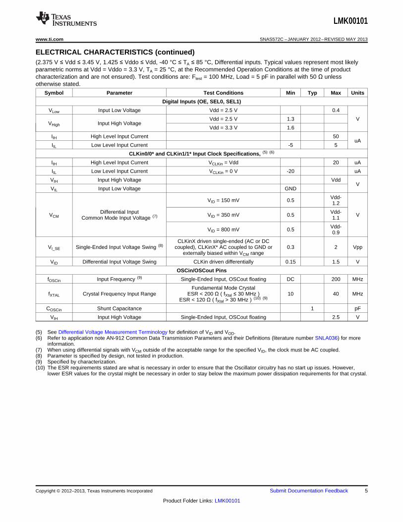
ELECTRICAL CHARACTERISTICS(2.375 V ≤ Vdd ≤ 3.45 V, 1.425 ≤ Vddo ≤ Vdd, -40 °C ≤ TA ≤ 85 °C, Differential inputs. Typical values represent most likelyparametric norms at Vdd = Vddo = 3.3 V, TA = 25 °C, at the Recommended Operation Conditions at the time of productcharacterization and are not ensured). Test conditions are: Ftest = 100 MHz, Load = 5 pF in parallel with 50 Ω unlessotherwise stated.
Symbol Parameter Test Conditions Min Typ Max Units
Total Device Characteristics
2.5 orVdd Core Supply Voltage 2.375 3.45 V3.3
1.5,1.8,Vddo Output Supply Voltage 1.425 2.5, or Vdd V
3.3
No CLKin 16 25
IVdd Core Current Vddo = 3.3 V, Ftest = 100 MHz 24 mA
Vddo = 2.5 V, Ftest = 100 MHz 20
Vddo = 2.5 V, 5OE = High, Ftest = 100 MHz
IVddo[n] Current for Each Output Vddo= 3.3 V, mA7OE = High, Ftest = 100 MHz
OE = Low 0.1
OE = High @ 100 MHz 95Total Device Current with Loads on allIVdd + IVddo mAoutputs OE = Low 16
Power Supply Ripple Rejection (PSRR)
100 kHz, 100 mVppRipple InducedPSRR Ripple Injected on -44 dBcPhase Spur Level Vdd, Vddo = 2.5 V
Outputs (1)
Measured between outputs,Skew Output Skew (2) 6 25 psreferenced to CLKout0
CL = 5 pF, RL = 50 Ω 0.85 1.4 2.2 nsVdd = 3.3 V; Vddo = 3.3 VPropagation DelaytPD CLKin to CLKout (2)CL = 5 pF, RL = 50 Ω 1.1 1.8 2.8 nsVdd = 2.5 V; Vddo = 1.5 V
CL = 5 pF, RL = 50 Ω 0.35 nsVdd = 3.3 V; Vddo = 3.3 VtPD, PP Part-to-part Skew (2) (3)
CL = 5 pF, RL = 50 Ω 0.6 nsVdd = 2.5 V; Vddo = 1.5 V
fCLKout Output Frequency (4) DC 200 MHz
Vdd = 3.3 V, Vddo = 1.8 V, CL = 10 pF 250
tRise Rise/Fall Time Vdd = 2.5 V, Vddo = 2.5 V, CL = 10 pF 275 ps
Vdd = 3.3 V, Vddo = 3.3 V, CL = 10 pF 315
VCLKoutLow Output Low Voltage 0.1VVddo-VCLKoutHigh Output High Voltage 0.1
RCLKout Output Resistance 50 ohm
fCLKout = 156.25 MHz,tj RMS Additive Jitter CMOS input slew rate ≥ 2 V/ns 30 fs
CL = 5 pF, BW = 12 kHz to 20 MHz
(1) AC Parameters for CMOS are dependent upon output capacitive loading(2) Parameter is specified by design, not tested in production.(3) Part-to-part skew is calculated as the difference between the fastest and slowest tPD across multiple devices.(4) Specified by characterization.
4 Submit Documentation Feedback Copyright © 2012–2013, Texas Instruments Incorporated
Product Folder Links: LMK00101
LMK00101
www.ti.com SNAS572C –JANUARY 2012–REVISED MAY 2013
ELECTRICAL CHARACTERISTICS (continued)(2.375 V ≤ Vdd ≤ 3.45 V, 1.425 ≤ Vddo ≤ Vdd, -40 °C ≤ TA ≤ 85 °C, Differential inputs. Typical values represent most likelyparametric norms at Vdd = Vddo = 3.3 V, TA = 25 °C, at the Recommended Operation Conditions at the time of productcharacterization and are not ensured). Test conditions are: Ftest = 100 MHz, Load = 5 pF in parallel with 50 Ω unlessotherwise stated.
Symbol Parameter Test Conditions Min Typ Max Units
Digital Inputs (OE, SEL0, SEL1)
VLow Input Low Voltage Vdd = 2.5 V 0.4
Vdd = 2.5 V 1.3 VVHigh Input High Voltage
Vdd = 3.3 V 1.6
IIH High Level Input Current 50uA
IIL Low Level Input Current -5 5
CLKin0/0* and CLKin1/1* Input Clock Specifications, (5) (6)
IIH High Level Input Current VCLKin = Vdd 20 uA
IIL Low Level Input Current VCLKin = 0 V -20 uA
VIH Input High Voltage VddV
VIL Input Low Voltage GND
Vdd-VID = 150 mV 0.5 1.2
Differential Input Vdd-VCM VID = 350 mV 0.5 VCommon Mode Input Voltage (7) 1.1
Vdd-VID = 800 mV 0.5 0.9
CLKinX driven single-ended (AC or DCVI_SE Single-Ended Input Voltage Swing (8) coupled), CLKinX* AC coupled to GND or 0.3 2 Vpp
externally biased within VCM range
VID Differential Input Voltage Swing CLKin driven differentially 0.15 1.5 V
OSCin/OSCout Pins
fOSCin Input Frequency (9) Single-Ended Input, OSCout floating DC 200 MHz
Fundamental Mode CrystalfXTAL Crystal Frequency Input Range ESR < 200 Ω ( fXtal ≤ 30 MHz ) 10 40 MHz
ESR < 120 Ω ( fXtal > 30 MHz ) (10) (9)
COSCin Shunt Capacitance 1 pF
VIH Input High Voltage Single-Ended Input, OSCout floating 2.5 V
(5) See Differential Voltage Measurement Terminology for definition of VID and VOD.(6) Refer to application note AN-912 Common Data Transmission Parameters and their Definitions (literature number SNLA036) for more
information.(7) When using differential signals with VCM outside of the acceptable range for the specified VID, the clock must be AC coupled.(8) Parameter is specified by design, not tested in production.(9) Specified by characterization.(10) The ESR requirements stated are what is necessary in order to ensure that the Oscillator circuitry has no start up issues. However,
lower ESR values for the crystal might be necessary in order to stay below the maximum power dissipation requirements for that crystal.
Copyright © 2012–2013, Texas Instruments Incorporated Submit Documentation Feedback 5
Product Folder Links: LMK00101

0 50 100 150 200 250
0
5
10
15
CU
RR
EN
T (
mA
)
FREQUENCY (MHz)
Cload = 10 pF
Vddo = 1.5 VVddo = 1.8 VVddo = 2.5 VVddo = 3.3 V
0 200 400 600 800 1000
0.0
0.5
1.0
1.5
2.0
2.5
3.0
3.5
OU
TP
UT
SW
ING
(V
)
FREQUENCY (MHz)
Rterm=50
Vddo=1.5 VVddo=1.8 VVddo=2.5 VVddo=3.3 V
LVCMOS Output
CLKin Source
0.5 1.0 1.5 2.0 2.5 3.0
0
50
100
150
200
250
300
350
400
450
500
RM
S J
ITT
ER
(fs
)
DIFFERENTIAL INPUT SLEW RATE (V/ns)
Fclk-100 MHzInt. BW=1-20 MHz
-40 C25 C85 CCLKin Source
0.5 1.0 1.5 2.0 2.5 3.0
-170
-165
-160
-155
-150
-145
-140
NO
ISE
FLO
OR
(dB
c/H
z)
DIFFERENTIAL INPUT SLEW RATE (V/ns)
Fclk=100 MHzFoffset=20 MHz
-40 C25 C85 CCLKin Source
LMK00101
SNAS572C –JANUARY 2012–REVISED MAY 2013 www.ti.com
TYPICAL PERFORMANCE CHARACTERISTICSUnless otherwise specified: Vdd = Vddo = 3.3 V, TA = 20 °C, CL = 5 pF, CLKin driven differentially, input slew rate ≥ 2 V/ns.
RMS Jitter vs. CLKin Slew Rate @ 100 MHz Noise Floor vs. CLKin Slew Rate @ 100 MHz
Figure 2. Figure 3.
LVCMOS Phase Noise @ 100 MHz LVCMOS Output Swing vs. Frequency
Test conditions: LVCMOS Input, slew rate ≥ 2 V/ns, CL = 5 pF inparallel with 50 Ω, BW = 1 MHz to 20 MHz
Figure 4. Figure 5.
Iddo per Output vs Frequency
Figure 6.
6 Submit Documentation Feedback Copyright © 2012–2013, Texas Instruments Incorporated
Product Folder Links: LMK00101

VOH
VOL
GND
VOD = | VOH - VOL | VSS = 2·VOD
VOD Definition VSS Definition for Output
Non-Inverting Clock
Inverting Clock
VOD VSSVOS
VIH
VIL
GND
VID = | VIH ± VIL | VSS = 2·VID
VID Definition VSS Definition for Input
Non-Inverting Clock
Inverting Clock
VID VSSVCM
LMK00101
www.ti.com SNAS572C –JANUARY 2012–REVISED MAY 2013
MEASUREMENT DEFINITIONS
Differential Voltage Measurement Terminology
The differential voltage of a differential signal can be described by two different definitions causing confusionwhen reading datasheets or communicating with other engineers. This section will address the measurement anddescription of a differential signal so that the reader will be able to understand and discern between the twodifferent definitions when used.
The first definition used to describe a differential signal is the absolute value of the voltage potential between theinverting and non-inverting signal. The symbol for this first measurement is typically VID or VOD depending on ifan input or output voltage is being described.
The second definition used to describe a differential signal is to measure the potential of the non-inverting signalwith respect to the inverting signal. The symbol for this second measurement is VSS and is a calculatedparameter. Nowhere in the IC does this signal exist with respect to ground, it only exists in reference to itsdifferential pair. VSS can be measured directly by oscilloscopes with floating references, otherwise this value canbe calculated as twice the value of VOD as described in the first section
Figure 7 illustrates the two different definitions side-by-side for inputs and Figure 8 illustrates the two differentdefinitions side-by-side for outputs. The VID and VOD definitions show VA and VB DC levels that the non-invertingand inverting signals toggle between with respect to ground. VSS input and output definitions show that if theinverting signal is considered the voltage potential reference, the non-inverting signal voltage potential is nowincreasing and decreasing above and below the non-inverting reference. Thus the peak-to-peak voltage of thedifferential signal can be measured.
VID and VOD are often defined in volts (V) and VSS is often defined as volts peak-to-peak (VPP).
Figure 7. Two Different Definitions for Differential Input Signals
Figure 8. Two Different Definitions for Differential Output Signals
Copyright © 2012–2013, Texas Instruments Incorporated Submit Documentation Feedback 7
Product Folder Links: LMK00101
LMK00101
SNAS572C –JANUARY 2012–REVISED MAY 2013 www.ti.com
FUNCTIONAL DESCRIPTION
The LMK00101 is a 10 output LVCMOS clock fanout buffer with low additive jitter that can operate up to 200MHz. It features a 3:1 input multiplexer with a crystal oscillator input, single supply or dual supply (lower power)operation, and pin-programmable device configuration. The device is offered in a 32-pin WQFN package.
Vdd and Vddo Power Supplies
Separate core and output supplies allow the output buffers to operate at the same supply as the Vdd core supply(3.3 V or 2.5 V) or from a lower supply voltage (3.3 V, 2.5 V, 1.8 V, or 1.5 V). Compared to single-supplyoperation, dual supply operation enables lower power consumption and output-level compatibility.
Bank A (CLKout0 to CLKout4) and Bank B (CLKout5 to CLKout9) may also be operated at different Vddovoltages, provided neither Vddo voltage exceeds Vdd.
NOTECare should be taken to ensure the Vddo voltage does not exceed the Vdd voltage toprevent turning-on the internal ESD protection circuitry.
DO NOT DISCONNECT OR GROUND ANY OF THE Vddo PINS as the Vddo pins areinternally connected within an output bank.
CLOCK INPUTS
The LMK00101 has three different inputs, CLKin0/CLKin0*, CLKin1/CLKin1*, and OSCin that can be driven indifferent manners that are described in the following sections.
SELECTION OF CLOCK INPUT
Clock input selection is controlled using the SEL0 and SEL1 pins as shown in Table 1. Refer to Driving the ClockInputs for clock input requirements. When CLKin0 or CLKin1 is selected, the crystal circuit is powered down.When OSCin is selected, the crystal oscillator will start-up and its clock will be distributed to all outputs. Refer toCrystal Interface for more information. Alternatively, OSCin may be driven by a single ended clock, up to 200MHz, instead of a crystal.
Table 1. Input Selection
SEL1 SEL0 Input
0 0 CLKin0, CLKin0*
0 1 CLKin1, CLKin1*
OSCin1 X (Crystal Mode)
CLKin/CLKin* Pins
The LMK00101 has two differential inputs (CLKin0/CLKin0* and CLKin1/CLKin1*) that can be driven single-ended or differentially. They can accept AC or DC coupled 3.3V/2.5V LVPECL, LVDS, or other differential andsingled ended signals that meet the input requirements under the “CLKin0/0* and CLKin1/1* Input ClockSpecifications” portion of the ELECTRICAL CHARACTERISTICS and (1). Refer to Driving the Clock Inputs formore details on driving the LMK00101 inputs.
In the event that a Crystal mode is not selected and the CLKin pins do not have an AC signal applied to them,Table 2 following will be the state of the outputs.(1) When using differential signals with VCM outside of the acceptable range for the specified VID, the clock must be AC coupled.
8 Submit Documentation Feedback Copyright © 2012–2013, Texas Instruments Incorporated
Product Folder Links: LMK00101

LMK00101
www.ti.com SNAS572C –JANUARY 2012–REVISED MAY 2013
Table 2. CLKinX Input vs. Output States
CLKinX CLKinX* Output State
Open Open Logic Low
Logic Low Logic Low Logic Low
Logic High Logic Low Logic High
Logic Low Logic High Logic Low
OSCin/OSCout Pins
The LMK00101 has a crystal oscillator which will be powered up when OSCin is selected. Alternatively, OSCinmay be driven by a single ended clock, up to 200 MHz, instead of a crystal. Refer to Crystal Interface for moreinformation.
If Crystal mode is selected and the pins do not have an AC signal applied to them, Table 3 will be the state of theoutputs. If Crystal mode is selected an open state is not allowed on OSCin, as the outputs may oscillate due tothe crystal oscillator circuitry.
Table 3. OSCin Input vs. Output States
OSCin Output State
Open Not Allowed
Logic Low Logic High
Logic High Logic Low
CLOCK OUTPUTS
The LMK00101 has 10 LVCMOS outputs.
Output Enable Pin
When the output enable pin is held High, the outputs are enabled. When it is held Low, the outputs are held in aLow state as shown in Table 4.
Table 4. Output Enable Pin States
OE Outputs
Low Disabled (Hi-Z)
High Enabled
The OE pin is synchronized to the input clock to ensure that there are no runt pulses. When OE is changed fromLow to High, the outputs will initially have an impedance of about 400 Ω to ground until the second falling edge ofthe input clock. Starting with the second falling edge of the input clock, the outputs will buffer the input. If the OEpin is taken from Low to High when there is no input clock present, the outputs will either go High or Low andstay a that state; they will not oscillate. When the OE pin is taken from High to Low the outputs will become Lowafter the second falling edge of the clock input and then will go to a Disabled (Hi-Z) state starting after the nextrising edge.
Using Less than Ten Outputs
Although the LMK00101 has 10 outputs, not all applications will require all of these. In this case, the unusedoutputs should be left floating with a minimum copper length to minimize capacitance. In this way, this output willconsume minimal output current because it has no load.
NOTEFor best soldering practices, the minimum trace length should extend to include the pinsolder mask. This way during reflow, the solder has the same copper area as connectedpins. This allows for good, uniform fillet solder joints helping to keep the IC level duringreflow.
Copyright © 2012–2013, Texas Instruments Incorporated Submit Documentation Feedback 9
Product Folder Links: LMK00101

0.1 PF
50:Trace CMOS Driver
Rs
VCC
RB1
RB2
VCC
LMKInput
50:
VO,PP VO,PP/2
VBB ~ (VO,PP/2) x 0.5
0.1 PF
0.1 PF
50:Trace50: LMK
Input
0.1 PFRSCMOSDriver
LMK00101
SNAS572C –JANUARY 2012–REVISED MAY 2013 www.ti.com
APPLICATION INFORMATION
Driving the Clock Inputs
The LMK00101 has two differential inputs (CLKin0/CLKin0* and CLKin1/CLKin1*) that can accept AC or DCcoupled 3.3V/2.5V LVPECL, LVDS, and other differential and single ended signals that meet the inputrequirements specified in ELECTRICAL CHARACTERISTICS. The device can accept a wide range of signalsdue to its wide input common mode voltage range (VCM) and input voltage swing (VID)/dynamic range. ACcoupling may also be employed to shift the input signal to within the VCM range.
To achieve the best possible phase noise and jitter performance, it is recommended that the input have a highslew rate of 2 V/ns(differential) or higher. Driving the input with a lower slew rate will degrade the noise floor andjitter. For this reason, a differential input signal is recommended over single-ended because it typically provideshigher slew rate and common-mode noise rejection.
While it is recommended to drive the CLKin/CLKin* pair with a differential signal input, it is possible to drive itwith a single-ended clock provided it conforms to the Single-Ended Input specifications for CLKin pins listed inthe Electrical Characteristics. For large single-ended input signals, such as 3.3V or 2.5V LVCMOS, a 50 Ω loadresistor should be placed near the input for signal attenuation to prevent input overdrive as well as for linetermination to minimize reflections. The CLKin input has an internal bias voltage of about 1.4 V, so the input canbe AC coupled as shown in Figure 9. The output impedance of the LVCMOS driver plus Rs should be close to50 Ω to match the characteristic impedance of the transmission line and load termination.
Figure 9. Preferred Configuration: Single-Ended LVCMOS Input, AC Coupling, Near and Far EndTermination
A single-ended clock may also be DC coupled to CLKinX as shown in Figure 10. A 50-Ω load resistor should beplaced near the CLKinX input for signal attenuation and line termination. Because half of the single-ended swingof the driver (VO,PP / 2) drives CLKinX, CLKinX* should be externally biased to the midpoint voltage of theattenuated input swing ((VO,PP / 2) × 0.5). The external bias voltage should be within the specified input commonvoltage (VCM) range. This can be achieved using external biasing resistors in the kΩ range (RB1 and RB2) oranother low-noise voltage reference. This will ensure the input swing crosses the threshold voltage at a pointwhere the input slew rate is the highest.
Figure 10. Single-Ended LVCMOS Input, DC Coupling with Common Mode Biasing
10 Submit Documentation Feedback Copyright © 2012–2013, Texas Instruments Incorporated
Product Folder Links: LMK00101

LMK
0010
1OSCin
OSCout
C1
C2
XTALRLIM
0.1 PF50:Trace
50:
CMOSDriver
0.1 PFRS
LMK
0010
1OSCin
OSCout
LMK00101
www.ti.com SNAS572C –JANUARY 2012–REVISED MAY 2013
If the crystal oscillator circuit is not used, it is possible to drive the OSCin input with an single-ended externalclock as shown in Figure 11. The input clock should be AC coupled to the OSCin pin, which has an internallygenerated input bias voltage, and the OSCout pin should be left floating. While OSCin provides an alternativeinput to multiplex an external clock, it is recommended to use either differential input (CLKinX) since it offershigher operating frequency, better common mode, improved power supply noise rejection, and greaterperformance over supply voltage and temperature variations.
Figure 11. Driving OSCin with a Single-Ended External Clock
Crystal Interface
The LMK00101 has an integrated crystal oscillator circuit that supports a fundamental mode, AT-cut crystal. Thecrystal interface is shown in Figure 12.
Figure 12. Crystal Interface
The load capacitance (CL) is specific to the crystal, but usually on the order of 18 to 20 pF. While CL is specifiedfor the crystal, the OSCin input capacitance (CIN = 1 pF typical) of the device and PCB stray capacitance (CSTRAY~ 1 to 3 pF) can affect the discrete load capacitor values, C1 and C2. For the parallel resonant circuit, the discretecapacitor values can be calculated as follows:
CL = (C1 * C2) / (C1 + C2) + CIN + CSTRAY (1)
Typically, C1 = C2 for optimum symmetry, so Equation 1 can be rewritten in terms of C1only:CL = C1
2 / (2 * C1 ) + CIN + CSTRAY (2)
Finally, solve for C1:C1 = (CL - CIN - CSTRAY) * 2 (3)
ELECTRICAL CHARACTERISTICS provides crystal interface specifications with conditions that ensure start-upof the crystal, but it does not specify crystal power dissipation. The designer will need to ensure the crystal powerdissipation does not exceed the maximum drive level specified by the crystal manufacturer. Overdriving thecrystal can cause premature aging, frequency shift, and eventual failure. Drive level should be held at a sufficientlevel necessary to start-up and maintain steady-state operation.
Copyright © 2012–2013, Texas Instruments Incorporated Submit Documentation Feedback 11
Product Folder Links: LMK00101
RippleSource
Bias-TeePower
Supplies
DUT Board
LimitingAmp
ScopePhase Noise
Analyzer
IC
Measure 100 mVPP ripple on Vddo at IC
OUT
OUT
Measure single sideband phase spur
power in dBc
Clock Source
IN+
IN-
VccoVcc
LMK00101
SNAS572C –JANUARY 2012–REVISED MAY 2013 www.ti.com
The power dissipated in the crystal, PXTAL, can be computed by:PXTAL = IRMS
2 * RESR * (1 + C0 / CL)2
Where:• IRMS is the RMS current through the crystal.• RESR is the maximum equivalent series resistance specified for the crystal.• CL is the load capacitance specified for the crystal.• C0 is the minimum shunt capacitance specified for the crystal. (4)
IRMS can be measured using a current probe (e.g. Tektronix CT-6 or equivalent) placed on the leg of the crystalconnected to OSCout with the oscillation circuit active.
As shown in Figure 12, an external resistor, RLIM, can be used to limit the crystal drive level if necessary. If thepower dissipated in the selected crystal is higher than the drive level specified for the crystal with RLIM shorted,then a larger resistor value is mandatory to avoid overdriving the crystal. However, if the power dissipated in thecrystal is less than the drive level with RLIM shorted, then a zero value for RLIM can be used. As a starting point, asuggested value for RLIM is 1.5 kΩ
Power Supply Ripple Rejection
In practical system applications, power supply noise (ripple) can be generated from switching power supplies,digital ASICs or FPGAs, etc. While power supply bypassing will help filter out some of this noise, it is important tounderstand the effect of power supply ripple on the device performance. When a single-tone sinusoidal signal isapplied to the power supply of a clock distribution device, such as LMK00101, it can produce narrow-band phasemodulation as well as amplitude modulation on the clock output (carrier). In the singleside band phase noisespectrum, the ripple-induced phase modulation appears as a phase spur level relative to the carrier (measured indBc).
For the LMK00101, power supply ripple rejection (PSRR), was measured as the single-sideband phase spurlevel (in dBc) modulated onto the clock output when a ripple signal was injected onto the Vddo supply. The PSRRtest setup is shown in Figure 13.
Figure 13. PSRR Test Setup
A signal generator was used to inject a sinusoidal signal onto the Vddo supply of the DUT board, and the peak-to-peak ripple amplitude was measured at the Vddo pins of the device. A limiting amplifier was used to removeamplitude modulation on the differential output clock and convert it to a single-ended signal for the phase noiseanalyzer. The phase spur level measurements were taken for clock frequencies of 100 MHz under the followingpower supply ripple conditions:• Ripple amplitude: 100 mVpp on Vddo = 2.5 V• Ripple frequency: 100 kHz
Assuming no amplitude modulation effects and small index modulation, the peak-to-peak deterministic jitter (DJ)can be calculated using the measured single-sideband phase spur level (PSRR) as follows:
DJ (ps pk-pk) = [(2 * 10(PSRR/20)) / (π * fclk)] * 1012 (5)
12 Submit Documentation Feedback Copyright © 2012–2013, Texas Instruments Incorporated
Product Folder Links: LMK00101
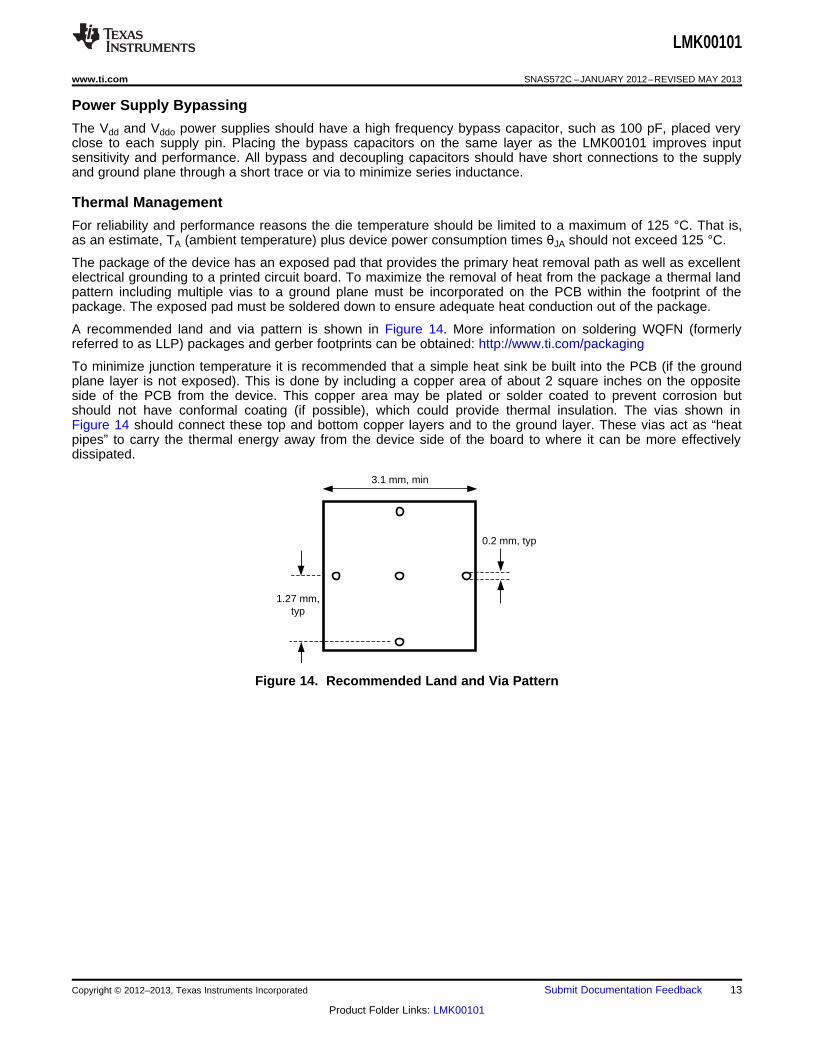
0.2 mm, typ
1.27 mm, typ
3.1 mm, min
LMK00101
www.ti.com SNAS572C –JANUARY 2012–REVISED MAY 2013
Power Supply Bypassing
The Vdd and Vddo power supplies should have a high frequency bypass capacitor, such as 100 pF, placed veryclose to each supply pin. Placing the bypass capacitors on the same layer as the LMK00101 improves inputsensitivity and performance. All bypass and decoupling capacitors should have short connections to the supplyand ground plane through a short trace or via to minimize series inductance.
Thermal Management
For reliability and performance reasons the die temperature should be limited to a maximum of 125 °C. That is,as an estimate, TA (ambient temperature) plus device power consumption times θJA should not exceed 125 °C.
The package of the device has an exposed pad that provides the primary heat removal path as well as excellentelectrical grounding to a printed circuit board. To maximize the removal of heat from the package a thermal landpattern including multiple vias to a ground plane must be incorporated on the PCB within the footprint of thepackage. The exposed pad must be soldered down to ensure adequate heat conduction out of the package.
A recommended land and via pattern is shown in Figure 14. More information on soldering WQFN (formerlyreferred to as LLP) packages and gerber footprints can be obtained: http://www.ti.com/packaging
To minimize junction temperature it is recommended that a simple heat sink be built into the PCB (if the groundplane layer is not exposed). This is done by including a copper area of about 2 square inches on the oppositeside of the PCB from the device. This copper area may be plated or solder coated to prevent corrosion butshould not have conformal coating (if possible), which could provide thermal insulation. The vias shown inFigure 14 should connect these top and bottom copper layers and to the ground layer. These vias act as “heatpipes” to carry the thermal energy away from the device side of the board to where it can be more effectivelydissipated.
Figure 14. Recommended Land and Via Pattern
Copyright © 2012–2013, Texas Instruments Incorporated Submit Documentation Feedback 13
Product Folder Links: LMK00101
LMK00101
SNAS572C –JANUARY 2012–REVISED MAY 2013 www.ti.com
REVISION HISTORY
Changes from Revision B (April 2013) to Revision C Page
• Deleted optional from CLKin1* pin description. Changed complimentary to complementary. ............................................. 2
• Added not tested in production to specified by design table note. ....................................................................................... 4
• Added max limit to Output Skew parameter and added tablenote to parameter in Electrical Characteristics Table. .......... 4
• Changed typical value for both conditions of Propagation Delay in the Electrical Characteristics Table ............................ 4
• Added Min/Max limits to both conditions of Propagation Delay parameter in Electrical Characteristics Table. .................. 4
• Changed both Max values of each Part-to-part Skew condition in Electrical Characteristics Table. ................................... 4
• Changed unit value for the first condition of Part-to-part Skew from ps to ns in the Electrical Characteristics Table. ........ 4
• Changed the Typ value of each Rise/Fall Time condition in the Electrical Characteristics Table ....................................... 4
• Added not tested in production to specified by design table note. ....................................................................................... 5
• Deleted VIL table note. ......................................................................................................................................................... 5
• Added VI_SE parameter and spec limits with corresponding table note to Electrical Characteristics Table. ........................ 5
• Changed third paragraph in Driving the Clock Inputs section to include CLKin* and LVCMOS text. Removed extrareferences to other figures. Revised to better correspond with information in Electrical Characteristics Table. ............... 10
• Deleted Figure 10 (Near End termination) and Figure 11 (Far End termination) from Driving the Clock Inputs section ... 10
• Changed bypass cap text with signal attenuation text in fourth paragraph of Driving the Clock Inputs. ........................... 10
• Changed Single-Ended LVCMOS Input, DC Coupling with Common Mode Biasing image with revised graphic. ............ 10
• Deleted two sentences in reference to two deleted images. .............................................................................................. 11
14 Submit Documentation Feedback Copyright © 2012–2013, Texas Instruments Incorporated
Product Folder Links: LMK00101

PACKAGE OPTION ADDENDUM
www.ti.com 3-May-2013
Addendum-Page 1
PACKAGING INFORMATION
Orderable Device Status(1)
Package Type PackageDrawing
Pins PackageQty
Eco Plan(2)
Lead/Ball Finish MSL Peak Temp(3)
Op Temp (°C) Top-Side Markings(4)
Samples
LMK00101SQ/NOPB ACTIVE WQFN RTV 32 1000 Green (RoHS& no Sb/Br)
CU SN Level-1-260C-UNLIM -40 to 85 K00101
LMK00101SQE/NOPB ACTIVE WQFN RTV 32 250 Green (RoHS& no Sb/Br)
CU SN Level-1-260C-UNLIM -40 to 85 K00101
LMK00101SQX/NOPB ACTIVE WQFN RTV 32 2500 Green (RoHS& no Sb/Br)
CU SN Level-1-260C-UNLIM -40 to 85 K00101
(1) The marketing status values are defined as follows:ACTIVE: Product device recommended for new designs.LIFEBUY: TI has announced that the device will be discontinued, and a lifetime-buy period is in effect.NRND: Not recommended for new designs. Device is in production to support existing customers, but TI does not recommend using this part in a new design.PREVIEW: Device has been announced but is not in production. Samples may or may not be available.OBSOLETE: TI has discontinued the production of the device.
(2) Eco Plan - The planned eco-friendly classification: Pb-Free (RoHS), Pb-Free (RoHS Exempt), or Green (RoHS & no Sb/Br) - please check http://www.ti.com/productcontent for the latest availabilityinformation and additional product content details.TBD: The Pb-Free/Green conversion plan has not been defined.Pb-Free (RoHS): TI's terms "Lead-Free" or "Pb-Free" mean semiconductor products that are compatible with the current RoHS requirements for all 6 substances, including the requirement thatlead not exceed 0.1% by weight in homogeneous materials. Where designed to be soldered at high temperatures, TI Pb-Free products are suitable for use in specified lead-free processes.Pb-Free (RoHS Exempt): This component has a RoHS exemption for either 1) lead-based flip-chip solder bumps used between the die and package, or 2) lead-based die adhesive used betweenthe die and leadframe. The component is otherwise considered Pb-Free (RoHS compatible) as defined above.Green (RoHS & no Sb/Br): TI defines "Green" to mean Pb-Free (RoHS compatible), and free of Bromine (Br) and Antimony (Sb) based flame retardants (Br or Sb do not exceed 0.1% by weightin homogeneous material)
(3) MSL, Peak Temp. -- The Moisture Sensitivity Level rating according to the JEDEC industry standard classifications, and peak solder temperature.
(4) Multiple Top-Side Markings will be inside parentheses. Only one Top-Side Marking contained in parentheses and separated by a "~" will appear on a device. If a line is indented then it is acontinuation of the previous line and the two combined represent the entire Top-Side Marking for that device.
Important Information and Disclaimer:The information provided on this page represents TI's knowledge and belief as of the date that it is provided. TI bases its knowledge and belief on informationprovided by third parties, and makes no representation or warranty as to the accuracy of such information. Efforts are underway to better integrate information from third parties. TI has taken andcontinues to take reasonable steps to provide representative and accurate information but may not have conducted destructive testing or chemical analysis on incoming materials and chemicals.TI and TI suppliers consider certain information to be proprietary, and thus CAS numbers and other limited information may not be available for release.
In no event shall TI's liability arising out of such information exceed the total purchase price of the TI part(s) at issue in this document sold by TI to Customer on an annual basis.

TAPE AND REEL INFORMATION
*All dimensions are nominal
Device PackageType
PackageDrawing
Pins SPQ ReelDiameter
(mm)
ReelWidth
W1 (mm)
A0(mm)
B0(mm)
K0(mm)
P1(mm)
W(mm)
Pin1Quadrant
LMK00101SQ/NOPB WQFN RTV 32 1000 178.0 12.4 5.3 5.3 1.3 8.0 12.0 Q1
LMK00101SQE/NOPB WQFN RTV 32 250 178.0 12.4 5.3 5.3 1.3 8.0 12.0 Q1
LMK00101SQX/NOPB WQFN RTV 32 2500 330.0 12.4 5.3 5.3 1.3 8.0 12.0 Q1
PACKAGE MATERIALS INFORMATION
www.ti.com 24-May-2017
Pack Materials-Page 1

*All dimensions are nominal
Device Package Type Package Drawing Pins SPQ Length (mm) Width (mm) Height (mm)
LMK00101SQ/NOPB WQFN RTV 32 1000 210.0 185.0 35.0
LMK00101SQE/NOPB WQFN RTV 32 250 210.0 185.0 35.0
LMK00101SQX/NOPB WQFN RTV 32 2500 367.0 367.0 35.0
PACKAGE MATERIALS INFORMATION
www.ti.com 24-May-2017
Pack Materials-Page 2

www.ti.com
PACKAGE OUTLINE
C
5.154.85
5.154.85
0.80.7
0.050.00
2X 3.5
28X 0.5
2X 3.5
32X 0.50.3
32X 0.300.18
3.1 0.1
(0.1) TYP
WQFN - 0.8 mm max heightRTV0032APLASTIC QUAD FLATPACK - NO LEAD
4224386/A 06/2018
0.08 C
0.1 C A B0.05
NOTES: 1. All linear dimensions are in millimeters. Any dimensions in parenthesis are for reference only. Dimensioning and tolerancing per ASME Y14.5M. 2. This drawing is subject to change without notice. 3. The package thermal pad must be soldered to the printed circuit board for thermal and mechanical performance.
PIN 1 INDEX AREA
SEATING PLANE
PIN 1 ID
SYMMEXPOSEDTHERMAL PAD
SYMM
1
8
9 16
17
24
2532
33
SCALE 2.500
AB

www.ti.com
EXAMPLE BOARD LAYOUT
28X (0.5)
(1.3)
(1.3)
(R0.05) TYP
0.07 MAXALL AROUND
0.07 MINALL AROUND
32X (0.6)
32X (0.24)
(4.8)
(4.8)
(3.1)
(3.1)
( 0.2) TYPVIA
WQFN - 0.8 mm max heightRTV0032APLASTIC QUAD FLATPACK - NO LEAD
4224386/A 06/2018
NOTES: (continued) 4. This package is designed to be soldered to a thermal pad on the board. For more information, see Texas Instruments literature number SLUA271 (www.ti.com/lit/slua271).5. Vias are optional depending on application, refer to device data sheet. If any vias are implemented, refer to their locations shown on this view. It is recommended that vias under paste be filled, plugged or tented.
SYMM
SYMM
SEE SOLDER MASKDETAIL
LAND PATTERN EXAMPLEEXPOSED METAL SHOWN
SCALE: 15X
1
8
9 16
17
24
2532
33
METAL EDGE
SOLDER MASKOPENING
EXPOSED METAL
METAL UNDERSOLDER MASK
SOLDER MASKOPENING
EXPOSEDMETAL
NON SOLDER MASKDEFINED
(PREFERRED)SOLDER MASK DEFINED
SOLDER MASK DETAILS

www.ti.com
EXAMPLE STENCIL DESIGN
32X (0.6)
32X (0.24)
28X (0.5)
(4.8)
(4.8)
(0.775) TYP
(0.775) TYP
4X (1.35)
4X (1.35)
(R0.05) TYP
WQFN - 0.8 mm max heightRTV0032APLASTIC QUAD FLATPACK - NO LEAD
4224386/A 06/2018
NOTES: (continued) 6. Laser cutting apertures with trapezoidal walls and rounded corners may offer better paste release. IPC-7525 may have alternate design recommendations.
SOLDER PASTE EXAMPLEBASED ON 0.125 MM THICK STENCIL
SCALE: 20X
EXPOSED PAD 3376% PRINTED SOLDER COVERAGE BY AREA UNDER PACKAGE
SYMM
SYMM
1
8
9 16
17
24
2532
33

IMPORTANT NOTICE
Texas Instruments Incorporated (TI) reserves the right to make corrections, enhancements, improvements and other changes to itssemiconductor products and services per JESD46, latest issue, and to discontinue any product or service per JESD48, latest issue. Buyersshould obtain the latest relevant information before placing orders and should verify that such information is current and complete.TI’s published terms of sale for semiconductor products (http://www.ti.com/sc/docs/stdterms.htm) apply to the sale of packaged integratedcircuit products that TI has qualified and released to market. Additional terms may apply to the use or sale of other types of TI products andservices.Reproduction of significant portions of TI information in TI data sheets is permissible only if reproduction is without alteration and isaccompanied by all associated warranties, conditions, limitations, and notices. TI is not responsible or liable for such reproduceddocumentation. Information of third parties may be subject to additional restrictions. Resale of TI products or services with statementsdifferent from or beyond the parameters stated by TI for that product or service voids all express and any implied warranties for theassociated TI product or service and is an unfair and deceptive business practice. TI is not responsible or liable for any such statements.Buyers and others who are developing systems that incorporate TI products (collectively, “Designers”) understand and agree that Designersremain responsible for using their independent analysis, evaluation and judgment in designing their applications and that Designers havefull and exclusive responsibility to assure the safety of Designers' applications and compliance of their applications (and of all TI productsused in or for Designers’ applications) with all applicable regulations, laws and other applicable requirements. Designer represents that, withrespect to their applications, Designer has all the necessary expertise to create and implement safeguards that (1) anticipate dangerousconsequences of failures, (2) monitor failures and their consequences, and (3) lessen the likelihood of failures that might cause harm andtake appropriate actions. Designer agrees that prior to using or distributing any applications that include TI products, Designer willthoroughly test such applications and the functionality of such TI products as used in such applications.TI’s provision of technical, application or other design advice, quality characterization, reliability data or other services or information,including, but not limited to, reference designs and materials relating to evaluation modules, (collectively, “TI Resources”) are intended toassist designers who are developing applications that incorporate TI products; by downloading, accessing or using TI Resources in anyway, Designer (individually or, if Designer is acting on behalf of a company, Designer’s company) agrees to use any particular TI Resourcesolely for this purpose and subject to the terms of this Notice.TI’s provision of TI Resources does not expand or otherwise alter TI’s applicable published warranties or warranty disclaimers for TIproducts, and no additional obligations or liabilities arise from TI providing such TI Resources. TI reserves the right to make corrections,enhancements, improvements and other changes to its TI Resources. TI has not conducted any testing other than that specificallydescribed in the published documentation for a particular TI Resource.Designer is authorized to use, copy and modify any individual TI Resource only in connection with the development of applications thatinclude the TI product(s) identified in such TI Resource. NO OTHER LICENSE, EXPRESS OR IMPLIED, BY ESTOPPEL OR OTHERWISETO ANY OTHER TI INTELLECTUAL PROPERTY RIGHT, AND NO LICENSE TO ANY TECHNOLOGY OR INTELLECTUAL PROPERTYRIGHT OF TI OR ANY THIRD PARTY IS GRANTED HEREIN, including but not limited to any patent right, copyright, mask work right, orother intellectual property right relating to any combination, machine, or process in which TI products or services are used. Informationregarding or referencing third-party products or services does not constitute a license to use such products or services, or a warranty orendorsement thereof. Use of TI Resources may require a license from a third party under the patents or other intellectual property of thethird party, or a license from TI under the patents or other intellectual property of TI.TI RESOURCES ARE PROVIDED “AS IS” AND WITH ALL FAULTS. TI DISCLAIMS ALL OTHER WARRANTIES ORREPRESENTATIONS, EXPRESS OR IMPLIED, REGARDING RESOURCES OR USE THEREOF, INCLUDING BUT NOT LIMITED TOACCURACY OR COMPLETENESS, TITLE, ANY EPIDEMIC FAILURE WARRANTY AND ANY IMPLIED WARRANTIES OFMERCHANTABILITY, FITNESS FOR A PARTICULAR PURPOSE, AND NON-INFRINGEMENT OF ANY THIRD PARTY INTELLECTUALPROPERTY RIGHTS. TI SHALL NOT BE LIABLE FOR AND SHALL NOT DEFEND OR INDEMNIFY DESIGNER AGAINST ANY CLAIM,INCLUDING BUT NOT LIMITED TO ANY INFRINGEMENT CLAIM THAT RELATES TO OR IS BASED ON ANY COMBINATION OFPRODUCTS EVEN IF DESCRIBED IN TI RESOURCES OR OTHERWISE. IN NO EVENT SHALL TI BE LIABLE FOR ANY ACTUAL,DIRECT, SPECIAL, COLLATERAL, INDIRECT, PUNITIVE, INCIDENTAL, CONSEQUENTIAL OR EXEMPLARY DAMAGES INCONNECTION WITH OR ARISING OUT OF TI RESOURCES OR USE THEREOF, AND REGARDLESS OF WHETHER TI HAS BEENADVISED OF THE POSSIBILITY OF SUCH DAMAGES.Unless TI has explicitly designated an individual product as meeting the requirements of a particular industry standard (e.g., ISO/TS 16949and ISO 26262), TI is not responsible for any failure to meet such industry standard requirements.Where TI specifically promotes products as facilitating functional safety or as compliant with industry functional safety standards, suchproducts are intended to help enable customers to design and create their own applications that meet applicable functional safety standardsand requirements. Using products in an application does not by itself establish any safety features in the application. Designers mustensure compliance with safety-related requirements and standards applicable to their applications. Designer may not use any TI products inlife-critical medical equipment unless authorized officers of the parties have executed a special contract specifically governing such use.Life-critical medical equipment is medical equipment where failure of such equipment would cause serious bodily injury or death (e.g., lifesupport, pacemakers, defibrillators, heart pumps, neurostimulators, and implantables). Such equipment includes, without limitation, allmedical devices identified by the U.S. Food and Drug Administration as Class III devices and equivalent classifications outside the U.S.TI may expressly designate certain products as completing a particular qualification (e.g., Q100, Military Grade, or Enhanced Product).Designers agree that it has the necessary expertise to select the product with the appropriate qualification designation for their applicationsand that proper product selection is at Designers’ own risk. Designers are solely responsible for compliance with all legal and regulatoryrequirements in connection with such selection.Designer will fully indemnify TI and its representatives against any damages, costs, losses, and/or liabilities arising out of Designer’s non-compliance with the terms and provisions of this Notice.
Mailing Address: Texas Instruments, Post Office Box 655303, Dallas, Texas 75265Copyright © 2018, Texas Instruments Incorporated


![S2S65P10 Data Sheet - Epson · Video3 Horizontal Synchronization input/output CH3DIN[7:0] CH3DOUT[7:0] 49,48,46,45, 44,43,41,40 I/O LVCMOS SCHMITT 2mA Video3 Data input/output CH3ODD](https://img.dokumen.tips/doc/110x75/5fc2a4132df656188f6772d6/s2s65p10-data-sheet-epson-video3-horizontal-synchronization-inputoutput-ch3din70.jpg)