Embed Size (px)
Citation preview

V20TM, V30TM
V20HLTM, V30HLTM
V40TM, V50TM
V40HLTM, V50HLTM
V33ATM
V53ATM
Document No. U11301EJ5V0UMJ1 (5th edition)Date Published September 2000 N CP(K)Printed in Japan
INSTRUCTION
16-BIT V SERIESTM
16-/8- AND 16-BIT MICROPROCESSORS
© 1996
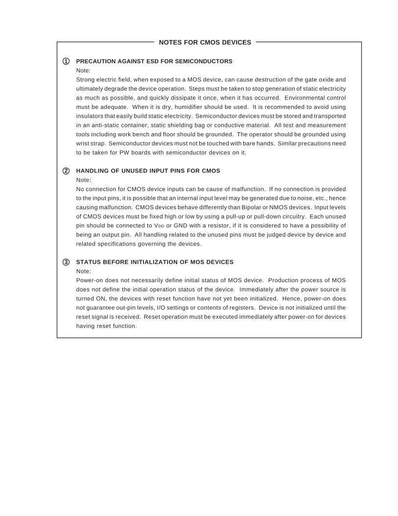
NOTES FOR CMOS DEVICES
1 PRECAUTION AGAINST ESD FOR SEMICONDUCTORS
Note:
Strong electric field, when exposed to a MOS device, can cause destruction of the gate oxide and
ultimately degrade the device operation. Steps must be taken to stop generation of static electricity
as much as possible, and quickly dissipate it once, when it has occurred. Environmental control
must be adequate. When it is dry, humidifier should be used. It is recommended to avoid using
insulators that easily build static electricity. Semiconductor devices must be stored and transported
in an anti-static container, static shielding bag or conductive material. All test and measurement
tools including work bench and floor should be grounded. The operator should be grounded using
wrist strap. Semiconductor devices must not be touched with bare hands. Similar precautions need
to be taken for PW boards with semiconductor devices on it.
2 HANDLING OF UNUSED INPUT PINS FOR CMOS
Note:
No connection for CMOS device inputs can be cause of malfunction. If no connection is provided
to the input pins, it is possible that an internal input level may be generated due to noise, etc., hence
causing malfunction. CMOS devices behave differently than Bipolar or NMOS devices. Input levels
of CMOS devices must be fixed high or low by using a pull-up or pull-down circuitry. Each unused
pin should be connected to VDD or GND with a resistor, if it is considered to have a possibility of
being an output pin. All handling related to the unused pins must be judged device by device and
related specifications governing the devices.
3 STATUS BEFORE INITIALIZATION OF MOS DEVICES
Note:
Power-on does not necessarily define initial status of MOS device. Production process of MOS
does not define the initial operation status of the device. Immediately after the power source is
turned ON, the devices with reset function have not yet been initialized. Hence, power-on does
not guarantee out-pin levels, I/O settings or contents of registers. Device is not initialized until the
reset signal is received. Reset operation must be executed immediately after power-on for devices
having reset function.

M8E 00. 4
The information in this document is current as of February, 1997. The information is subject to change without notice. For actual design-in, refer to the latest publications of NEC's data sheets or data books, etc., for the most up-to-date specifications of NEC semiconductor products. Not all products and/or types are available in every country. Please check with an NEC sales representative for availability and additional information.No part of this document may be copied or reproduced in any form or by any means without prior written consent of NEC. NEC assumes no responsibility for any errors that may appear in this document.NEC does not assume any liability for infringement of patents, copyrights or other intellectual property rights of third parties by or arising from the use of NEC semiconductor products listed in this document or any other liability arising from the use of such products. No license, express, implied or otherwise, is granted under any patents, copyrights or other intellectual property rights of NEC or others.Descriptions of circuits, software and other related information in this document are provided for illustrative purposes in semiconductor product operation and application examples. The incorporation of these circuits, software and information in the design of customer's equipment shall be done under the full responsibility of customer. NEC assumes no responsibility for any losses incurred by customers or third parties arising from the use of these circuits, software and information.While NEC endeavours to enhance the quality, reliability and safety of NEC semiconductor products, customers agree and acknowledge that the possibility of defects thereof cannot be eliminated entirely. To minimize risks of damage to property or injury (including death) to persons arising from defects in NEC semiconductor products, customers must incorporate sufficient safety measures in their design, such as redundancy, fire-containment, and anti-failure features.NEC semiconductor products are classified into the following three quality grades:"Standard", "Special" and "Specific". The "Specific" quality grade applies only to semiconductor products developed based on a customer-designated "quality assurance program" for a specific application. The recommended applications of a semiconductor product depend on its quality grade, as indicated below. Customers must check the quality grade of each semiconductor product before using it in a particular application. "Standard": Computers, office equipment, communications equipment, test and measurement equipment, audio
and visual equipment, home electronic appliances, machine tools, personal electronic equipmentand industrial robots
"Special": Transportation equipment (automobiles, trains, ships, etc.), traffic control systems, anti-disastersystems, anti-crime systems, safety equipment and medical equipment (not specifically designedfor life support)
"Specific": Aircraft, aerospace equipment, submersible repeaters, nuclear reactor control systems, lifesupport systems and medical equipment for life support, etc.
The quality grade of NEC semiconductor products is "Standard" unless otherwise expressly specified in NEC's data sheets or data books, etc. If customers wish to use NEC semiconductor products in applications not intended by NEC, they must contact an NEC sales representative in advance to determine NEC's willingness to support a given application.(Note)(1) "NEC" as used in this statement means NEC Corporation and also includes its majority-owned subsidiaries.(2) "NEC semiconductor products" means any semiconductor product developed or manufactured by or for
NEC (as defined above).
•
•
•
•
•
•
V20, V30, V20HL, V30HL, V40, V50, V40HL, V50HL, V33A, V53A, and V series are trademarks of NEC
Corporation.
InterTool is a trademark of Intermetrics Microsystems Software, Inc.

Regional Information
Some information contained in this document may vary from country to country. Before using any NECproduct in your application, pIease contact the NEC office in your country to obtain a list of authorizedrepresentatives and distributors. They will verify:
• Device availability
• Ordering information
• Product release schedule
• Availability of related technical literature
• Development environment specifications (for example, specifications for third-party tools and components, host computers, power plugs, AC supply voltages, and so forth)
• Network requirements
In addition, trademarks, registered trademarks, export restrictions, and other legal issues may also varyfrom country to country.
NEC Electronics Inc. (U.S.)Santa Clara, CaliforniaTel: 408-588-6000 800-366-9782Fax: 408-588-6130 800-729-9288
NEC Electronics (Germany) GmbHDuesseldorf, GermanyTel: 0211-65 03 02Fax: 0211-65 03 490
NEC Electronics (UK) Ltd.Milton Keynes, UKTel: 01908-691-133Fax: 01908-670-290
NEC Electronics Italiana s.r.l.Milano, ItalyTel: 02-66 75 41Fax: 02-66 75 42 99
NEC Electronics (Germany) GmbHBenelux OfficeEindhoven, The NetherlandsTel: 040-2445845Fax: 040-2444580
NEC Electronics (France) S.A.Velizy-Villacoublay, FranceTel: 01-30-67 58 00Fax: 01-30-67 58 99
NEC Electronics (France) S.A.Madrid OfficeMadrid, SpainTel: 91-504-2787Fax: 91-504-2860
NEC Electronics (Germany) GmbHScandinavia OfficeTaeby, SwedenTel: 08-63 80 820Fax: 08-63 80 388
NEC Electronics Hong Kong Ltd.Hong KongTel: 2886-9318Fax: 2886-9022/9044
NEC Electronics Hong Kong Ltd. Seoul BranchSeoul, KoreaTel: 02-528-0303Fax: 02-528-4411
NEC Electronics Singapore Pte. Ltd.United Square, SingaporeTel: 65-253-8311Fax: 65-250-3583
NEC Electronics Taiwan Ltd.Taipei, TaiwanTel: 02-2719-2377Fax: 02-2719-5951
NEC do Brasil S.A.Electron Devices DivisionGuarulhos-SP BrasilTel: 55-11-6462-6810Fax: 55-11-6462-6829
J00.7

MAJOR REVISIONS IN THIS EDITION
Pages Contents
Throughout The following products have been deleted:
• µPD70208 (A) (V40)
• µPD70216 (A) (V50)
• µPD70270 (V41TM)
• µPD70280 (V51TM)
The mark shows major revised points.

PREFACE
Readers This manual is intended for engineers who wish to understand the functions of the
following 16-bit V series microprocessors and design application systems using them.
Parts Number Nick Name
µPD70108 V20
µPD70116 V30
µPD70108H V20HL
µPD70116H V30HL
µPD70208 V40
µPD70216 V50
µPD70208H V40HL
µPD70216H V50HL
µPD70136A V33A
µPD70236A V53A
Purpose This manual is to introduce the instruction functions of the above 16-bit V series
microprocessors.
Organization Two volumes of the User’s Manual of the above 16- bit V series microprocessors are
available: Hardware Manual and Instruction Manual (this manual).
Hardware Manual Instruction Manual
General General
Pin Function Instruction Description
CPU Function Instruction Map
Internal Block Function Correspondence of Mnemonic between µPD8086 and 8088
Bus Control Function
Interrupt Function
Standby Function
Reset Function
Others

How to Read This Manual It is assumed that readers of this manual have a basic knowledge of electricity, logic
circuits, and microcontrollers. Unless otherwise specified, the descriptions in this
manual apply to all the models in the 16-bit V series microprocessors. Note that part
number “µPD70...” is referred to as “V...” in this manual.
To check the details of the function of an instruction whose mnemonic is known,
→ Refer to CHAPTER 2 INSTRUCTIONS (instructions are shown in alphabetic order
of the mnemonic)
To understand the details of each instruction,
→ Read this manual in the order of the Table of Contents.
To understand the hardware functions of each product,
→ Refer to the User’s Manual - Hardware (separate volume) for each product.
To find the electrical specifications
→ Refer to the data sheet for each product.
Legend Data significance : Left: high, right: low
Active low : ××× (top bar over pin or signal name)
Memory map address : Top: high, bottom: low
Address representation : x indicates a segment value, and y indicates an offset value
in the following case:
x: yH
Note : Explanation of items marked with Note in the text
Caution : Important information
Remark : Supplement
Numeric notation : Binary ... ×××× or ××××B
Decimal ... ××××Hexadecimal ... ××××H

Related documents The documents referred to in this publication may include preliminary versions. However,
preliminary versions are not marked as such.
Document Data Sheet User’s Manual Application Note Register Q & A
Parts Number Hardware Instruction Table
V20 IC-1827 IEM-871 This – – –
V30 IC-1828 manual
V20HL IC-3552 IEU-761 – – –
V30HL
V40 U10154E U10666E U10911E – U10554E
V50 Software
V40HL IC-3659 U11610E U10037E – U11123E
Hardware Design
V50HL U10911E
Software
V33A U10136E U10032E – – –
V53A U10120E U10108E U10188E – U10875E
Address Expansion,
Software

[MEMO]

– i –
TABLE OF CONTENTS
CHAPTER 1 GENERAL ............................................................................................................. ............... 11.1 Classification of Instructions by Function ........................................................................ 21.2 Instruction Word Format ..................................................................................................... 31.3 Functional Outline of Each Instruction .............................................................................. 3
1.3.1 Data transfer instructions ........................................................................................................... 3
1.3.2 Block manipulation instructions .................................................................................................. 3
1.3.3 Bit field manipulation instructions ............................................................................................... 3
1.3.4 I/O instructions ........................................................................................................................... 4
1.3.5 Operation instructions ................................................................................................................ 4
1.3.6 BCD operation instructions ........................................................................................................ 4
1.3.7 BCD adjustment instructions ...................................................................................................... 5
1.3.8 Data conversion instruction ........................................................................................................ 5
1.3.9 Bit manipulation instructions ...................................................................................................... 5
1.3.10 Shift and rotate instructions ........................................................................................................ 5
1.3.11 Stack manipulation instructions .................................................................................................. 5
1.3.12 Program branch instructions ...................................................................................................... 6
1.3.13 CPU control instructions ............................................................................................................. 6
1.3.14 Mode select instructions ............................................................................................................. 6
CHAPTER 2 INSTRUCTIONS ................................................................................................................... 72.1 Description of Instructions (in alphabetical order of mnemonic) ....................................72.2 Number of Instruction Execution Clocks ....................................................................... 169
APPENDIX A REGISTER CONFIGURATION ....................................................................................... 185A.1 General-Purpose Registers (AW, BW, CW, DW)............................................................ 185A.2 Segment Registers (PS, SS, DS0, DS1) .......................................................................... 185A.3 Pointers (SP, BP) ........................................................................................................... .. 185A.4 Program Counter (PC) ..................................................................................................... 185A.5 Program Status Word (PSW)........................................................................................... 186A.6 Index Registers (IX, IY) .................................................................................................... 190
APPENDIX B ADDRESSING MODES .................................................................................................. 1 91B.1 Instruction Address ......................................................................................................... 191B.2 Memory Operand Address .............................................................................................. 193
APPENDIX C INSTRUCTION MAP .................................................................................................... ... 199
APPENDIX D CORRESPONDENCE OF MNEMONICS OF µPD8086 AND 8088 ................................203
APPENDIX E INSTRUCTION INDEX (mnemonic: by function) .......................................................... 205
APPENDIX F INSTRUCTION INDEX (mnemonic: alphabetical order) .............................................. 207

– ii –
LIST OF FIGURES
Figure No. Title Page
1-1 Relations between Common Instructions and Dedicated Instructions of Each Model ........................... 1
1-2 Instruction Format .................................................................................................................................. 3
1-3 Operation of ALU When Operation Instruction Is Executed ................................................................... 4
2-1 Description Example ............................................................................................................................ 12
A-1 PSW Configuration............................................................................................................................. 186
LIST OF TABLES
Table No. Title Page
1-1 Classification of Instructions by Function ............................................................................................... 2
2-1 Example of Flag Operation .................................................................................................................... 7
2-2 Example of Operand Type ..................................................................................................................... 8
2-3 Example of Instruction Word .................................................................................................................. 9
2-4 Legend of Description of Instruction Format and Operand .................................................................. 10
2-5 Memory Addressing ............................................................................................................................. 11
2-6 Selecting 8-/16-Bit General-Purpose Register ..................................................................................... 11
2-7 Selecting Segment Register ................................................................................................................. 11
2-8 Number of Instruction Execution Clocks ............................................................................................ 170
C-1 Instruction Map................................................................................................................................... 200
C-2 Group1, Group2, Imm, and Shift Codes ............................................................................................ 202
C-3 Group0 Codes .................................................................................................................................... 202
C-4 Group3 Codes .................................................................................................................................... 202
D-1 Register Correspondence with µPD8086 and 8088 ........................................................................... 203
D-2 Mnemonic Correspondence with µPD8086 and 8088 ....................................................................... 204

1
CHAPTER 1 GENERAL
The 16-bit V series microprocessors have 101 common instructions that are completely compatible in terms of
software, so that your software resources can be effectively utilized.
In addition to these common instructions, the V20, V30, V20HL, V30HL, V40, V50, V40HL, and V50HL have three
dedicated instructions (BRKEM, RETEM, and CALLN) to support emulation mode.
The V33A and V53A have two dedicated instructions (BRKXA and RETXA) to support the extended address mode.
Figure 1-1. Relations between Common Instructions and Dedicated Instructions of Each Model
Remark For the emulation mode and extended address mode, refer to the Hardware Manual of each model.
V20, V30, V20HL, V30HL,V40 V50 V40HL, V50HL,
V33A, V53A
Dedicated emulationmode instructions
BRKEMRETEMCALLN
16-bit V series common instructions (101 types)
Dedicated extendedaddress mode
instructionsBRKXARETXA

2
CHAPTER 1 GENERAL
1.1 Classification of Instructions by Function
The instructions of the 16-bit V series can be broadly divided by classification of function into the following 27 types.
Table 1-1. Classification of Instructions by Function
Instruction Group Mnemonic (alphabetical order)
Data transfer instructions LDEA, MOV, TRANS, TRANSB, XCH
Repeat prefix REP, REPC, REPE, REPNC, REPNE, REPNZ, REPZ
Primitive block transfer instructions CMPBK, CMPBKB, CMPBKW, CMPM, CMPMB, CMPMW, LDM, LDMB,
LDMW, MOVBK, MOVBKB, MOVBKW, STM, STMB, STMW
Bit field manipulation instructions EXT, INS
I/O instructions IN, OUT
Primitive I/O instructions INM, OUTM
Add/subtract instructions ADD, ADDC, SUB, SUBC
BCD operation instructions ADD4S, CMP4S, ROL4, ROR4, SUB4S
Increment/decrement instructions DEC, INC
Multiplication/division instructions DIV, DIVU, MUL, MULU
BCD adjustment instructions ADJ4A, ADJ4S, ADJBA, ADJBS
Data conversion instructions CVTBD, CVTBW, CVTDB, CVTWL
Compare instructions CMP
Complement operation instructions NEG, NOT
Logical operation instructions AND, OR, TEST, XOR
Bit manipulation instructions CLR1, NOT1, SET1, TEST1
Shift instructions SHL, SHR, SHRA
Rotate instructions ROL, ROLC, ROR, RORC
Subroutine control instructions CALL, RET
Stack manipulation instructions DISPOSE, POP, PREPARE, PUSH
Branch instruction BR
Conditional branch instructions BC, BCWZ, BE, BGE, BGT, BH, BL, BLE, BLT, BN, BNC, BNE, BNH,
BNL, BNV, BNZ, BP, BPE, BPO, BZ, BV, DBNZ, DBNZE, DBNZNE
Interrupt instructions BRK, BRKV, CHKIND, RETI
CPU control instructions BUSLOCK, DI, EI, FPO1, FPO2, HALT, NOP, POLL
Segment override prefix DS0:, DS1:, PS:, SS:
Dedicated emulation mode instructionsNote 1 BRKEM, CALLN, RETEM
Dedicated extended address mode instructionsNote 2 BRKXA, RETXA
Notes 1. Except V33A and V53A
2. V33A and V53A only
3
CHAPTER 1 GENERAL
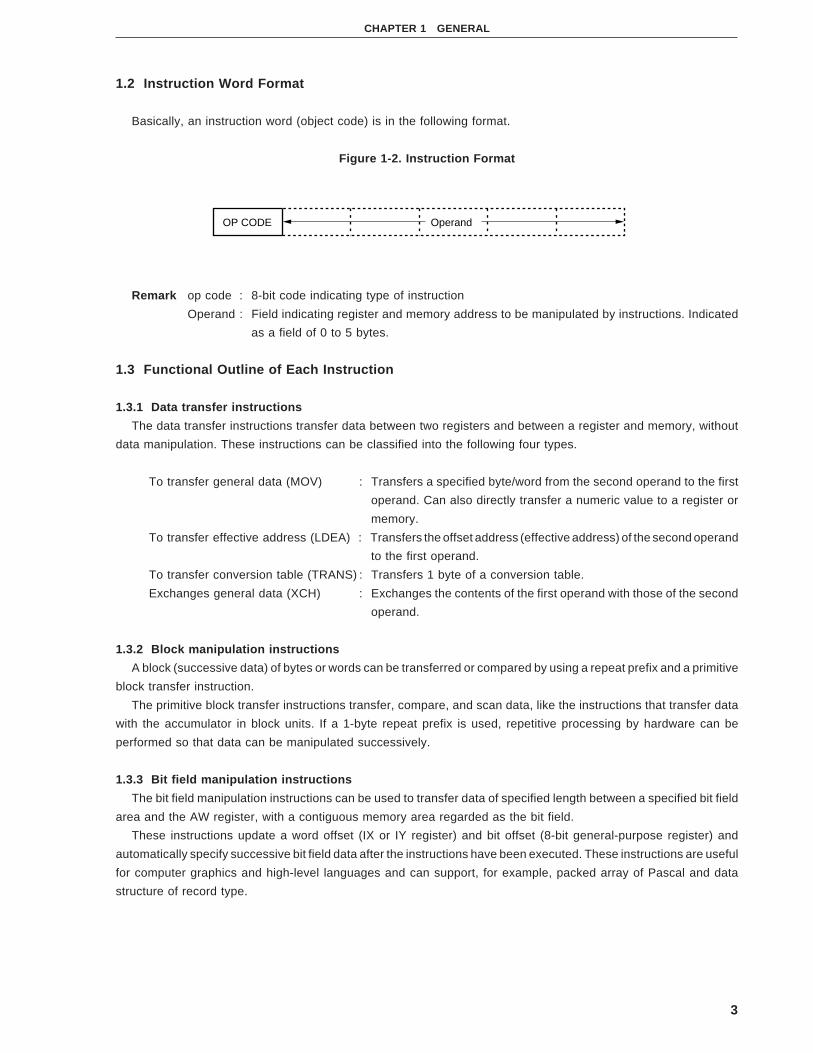
1.2 Instruction Word Format
Basically, an instruction word (object code) is in the following format.
Figure 1-2. Instruction Format
Remark op code : 8-bit code indicating type of instruction
Operand : Field indicating register and memory address to be manipulated by instructions. Indicated
as a field of 0 to 5 bytes.
1.3 Functional Outline of Each Instruction
1.3.1 Data transfer instructions
The data transfer instructions transfer data between two registers and between a register and memory, without
data manipulation. These instructions can be classified into the following four types.
To transfer general data (MOV) : Transfers a specified byte/word from the second operand to the first
operand. Can also directly transfer a numeric value to a register or
memory.
To transfer effective address (LDEA) : Transfers the offset address (effective address) of the second operand
to the first operand.
To transfer conversion table (TRANS) : Transfers 1 byte of a conversion table.
Exchanges general data (XCH) : Exchanges the contents of the first operand with those of the second
operand.
1.3.2 Block manipulation instructions
A block (successive data) of bytes or words can be transferred or compared by using a repeat prefix and a primitive
block transfer instruction.
The primitive block transfer instructions transfer, compare, and scan data, like the instructions that transfer data
with the accumulator in block units. If a 1-byte repeat prefix is used, repetitive processing by hardware can be
performed so that data can be manipulated successively.
1.3.3 Bit field manipulation instructions
The bit field manipulation instructions can be used to transfer data of specified length between a specified bit field
area and the AW register, with a contiguous memory area regarded as the bit field.
These instructions update a word offset (IX or IY register) and bit offset (8-bit general-purpose register) and
automatically specify successive bit field data after the instructions have been executed. These instructions are useful
for computer graphics and high-level languages and can support, for example, packed array of Pascal and data
structure of record type.
OP CODE Operand
4
CHAPTER 1 GENERAL
1.3.4 I/O instructions
The I/O instructions and primitive I/O instructions can read/write I/O devices.
The I/O devices transfer data with the CPU via the data bus by using these instructions.
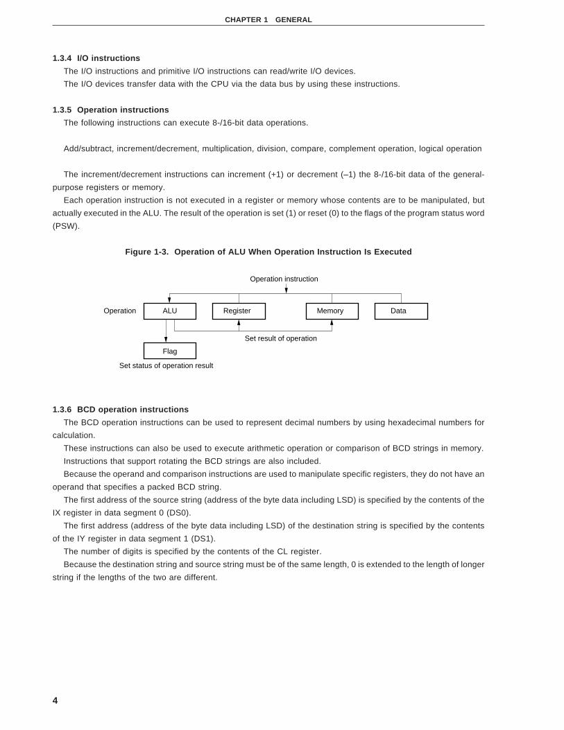
1.3.5 Operation instructions
The following instructions can execute 8-/16-bit data operations.
Add/subtract, increment/decrement, multiplication, division, compare, complement operation, logical operation
The increment/decrement instructions can increment (+1) or decrement (–1) the 8-/16-bit data of the general-
purpose registers or memory.
Each operation instruction is not executed in a register or memory whose contents are to be manipulated, but
actually executed in the ALU. The result of the operation is set (1) or reset (0) to the flags of the program status word
(PSW).
Figure 1-3. Operation of ALU When Operation Instruction Is Executed
1.3.6 BCD operation instructions
The BCD operation instructions can be used to represent decimal numbers by using hexadecimal numbers for
calculation.
These instructions can also be used to execute arithmetic operation or comparison of BCD strings in memory.
Instructions that support rotating the BCD strings are also included.
Because the operand and comparison instructions are used to manipulate specific registers, they do not have an
operand that specifies a packed BCD string.
The first address of the source string (address of the byte data including LSD) is specified by the contents of the
IX register in data segment 0 (DS0).
The first address (address of the byte data including LSD) of the destination string is specified by the contents
of the IY register in data segment 1 (DS1).
The number of digits is specified by the contents of the CL register.
Because the destination string and source string must be of the same length, 0 is extended to the length of longer
string if the lengths of the two are different.
Operation ALU Register Memory Data
Flag
Operation instruction
Set result of operation
Set status of operation result

5
CHAPTER 1 GENERAL
1.3.7 BCD adjustment instructions
BCD operation is supported by executing a BCD adjustment instruction before or after arithmetic operation.
Because the BCD adjustment instructions are executed on the AL register, they do not have an operand. In the
case of addition and subtraction, adjustment can be made to both packed BCD and unpacked BCD. In the case of
multiplication and division, however, adjustment can be made to only unpacked BCD representation.
1.3.8 Data conversion instruction
The data conversion instructions can convert the type and word length of binary and decimal numbers.
The CVTBD and CVTDB instructions convert binary numbers and 2-digit unpacked BCD.
The CVTBW and CVTWL instructions extend the sign in a register.
1.3.9 Bit manipulation instructions
The bit manipulation instructions are used to execute logical operations on the bit data of the general-purpose
registers or memory.
The operand of the instruction format is “reg, bit” or “mem, bit”.
The first operand, reg or mem, specifies 8-/16-bit data including the bit data to be manipulated and codes a general-
purpose register or an effective address.
The second operand bit indicates the address of the bit data in a byte or word, and uses the contents of CL or
8-bit immediate data. If reg or mem is 8-bit data, only the low-order 3 bits are the valid bit address. If reg or mem
is 16-bit data, only the low-order 4 bits are the valid bit address, and the high-order bits are ignored.
1.3.10 Shift and rotate instructions
The shift or rotate instructions shift or rotate the 8-/16-bit data of a general-purpose register or memory 1 bit or
more (0 to 255).
The shift instructions are divided into arithmetic shift and logical shift instructions. Usually, the number of digits
to be shifted is 1, but it can be changed depending on the value of the CL register each time the instruction has been
executed if specified by the count operand of the instruction (255 max.). The arithmetic shift instruction inserts 0 to
the LSB of the data shifted if the data has been shifted 1 bit to the left, and 1 to the MSB of the data if the data has
been shifted 1 bit to the right. The logical shift instruction does not cause the value of the LSB or MSB to be changed
even when the data has been shifted 1 bit.
Like the shift instructions, the number of digits to be rotated by a rotate instruction is specified by the count operand
of the instruction. This value is the value stored to the CL register. As a result of executing the rotate instruction, the
CY and V flags are affected. The bit rotated out is always stored to the CY flag. The V flag always becomes undefined
if two or more digits have been rotated. If only one digit is rotated and the MSB (extension) of the destination is affected
as a result, the V flag is set to 1; otherwise, the flag is reset to 0. The CY flag can be used as the extension of the
destination when the ROLC or ROR instruction is used.
1.3.11 Stack manipulation instructions
The stack manipulation instructions are used to manipulate the stack in the memory.
The following four types of stack manipulation instructions are available.
PUSH : Saves data to the stack.
POP : Restores data from the stack.
PREPARE : Creates a stack frame and copies a frame pointer to secure an area for a local variable or to
reference a global variable.
DISPOSE : Restores the stack pointer (SP) and base pointer (BP) to the status before the PREPARE
instruction is executed.

6
CHAPTER 1 GENERAL
1.3.12 Program branch instructions
These instructions branch program execution to specified addresses. The following four types of branch
instructions are available.
Subroutine control instructions : Save the contents of the program counter (PC) to the stack (CALL) or restore
the contents of the PC from the stack (RET).
Branch instruction : Branches the flow of an instruction to a specified address.
Conditional branch instructions : Branch the flow of instruction execution to a specified address depending
on the value of a flag.
Interrupt instructions : Temporarily stop execution of the program and controls flow of program
execution by means of software interrupts if an external device requests for
interrupt or if an operation error occurs.
1.3.13 CPU control instructions
The CPU control instructions manipulate flags, synchronize the processor with an external device, or transfer data.
An instruction that causes the CPU to execute nothing (NOP) is also available.
1.3.14 Mode select instructions
(1) Emulation mode (except V33A and V53A)
The mode can be changed between the native and emulation modes by using a dedicated emulation mode
instruction.
(2) Extended address mode (V33A and V53A only)
The mode can be changed between the normal address mode and extended address mode by using a
dedicated extended address mode instruction.

7
CHAPTER 2 INSTRUCTIONS
2.1 Description of Instructions (in alphabetical order of mnemonic)
This chapter explains the following items for each instruction.
[Format]
[Operation]
[Operand]
[Flag]
[Description]
[Example]
[Number of bytes]
[Word format]
In [Format], [Operation], and [Operand], several identifiers are used.
Tables 2-2 through 2-4 show the identifiers used and their meanings, and Tables 2-5 through 2-7 explain how to
select memory addressing modes, general-purpose registers, and segment registers.
[Flag] shows, by using identifiers, the operations of the flags that are affected as a result of executing the given
instruction. Table 2-1 shows examples of operations of each flag.
Table 2-1. Example of Flag Operation
Identifier Description
Blank Not affected
0 Reset to 0
1 Set to 1
× Set to 1 or reset to 0 depending on result
U Undefined
R Restores previously saved value

8
CHAPTER 2 INSTRUCTIONS
Table 2-2. Example of Operand Type
Identifier Description
reg 8-/16-bit general-purpose register
(destination register for instruction using two 8-/16-bit general-purpose registers)
reg’ Source register for instruction using two 8-/16-bit general-purpose registers
reg8 8-bit general-purpose register
(destination register for instruction using two 8-bit general-purpose registers)
reg8’ Source register for instruction using two 8-bit general-purpose registers
reg16 16-bit general-purpose register
(destination register for instruction using two 16-bit general-purpose registers)
reg16’ Source register for instruction using two 16-bit general-purpose registers
mem 8-/16-bit memory address
mem8 8-bit memory address
mem16 16-bit memory address
mem32 32-bit memory address
dmem 16-bit direct memory address
imm 8-/16-bit immediate data
imm3 3-bit immediate data
imm4 4-bit immediate data
imm8 8-bit immediate data
imm16 16-bit immediate data
acc Accumulator (AW or AL)
sreg Segment register
src-table Name of 256-byte conversion table
src-block Name of source block addressed by IX register
dst-block Name of destination block addressed by IY register
near-proc Procedure in current program segment
far-proc Procedure in other program segments
near-label Label in current program segment
short-label Label in range of end of instruction –128 to +127 bytes
far-label Label in other program segments
regptr16 16-bit general-purpose register having offset of call address in current program segment
memptr16 16-bit memory address having offset of call address in current program segment
memptr32 32-bit memory address having offset and segment data of call address in other program segments
pop-value Number of bytes discarded from stack (0 to 64K, usually even number)
fp-op Immediate value identifying instruction code of floating-point coprocessor
R Register set (AW, BW, CW, DW, SP, BP, IX, IY)
DS1-spec DS1 or segment name/group name ASSUMEd to DS1
Seg-spec Any segment register name or segment name/group name ASSUMEd to segment register
[ ] Can be omitted

9
CHAPTER 2 INSTRUCTIONS
Table 2-3. Example of Instruction Word
Identifier Description
W Byte/word field (0, 1)
reg Register field (000 to 111)
reg’ Register field (000 to 111) (source register for instruction using two registers)
mod, mem Memory addressing specification bit (mod: 00 to 10, mem: 000 to 111)
(disp-low) Low-order byte of option 16-bit displacement
(disp-high) High-order byte of option 16-bit displacement
disp-low Low-order byte of 16-bit displacement for PC relative addition
disp-high High-order byte of 16-bit displacement for PC relative addition
imm3 3-bit immediate data
imm4 4-bit immediate data
imm8 8-bit immediate data
imm16-low Low-order byte of 16-bit immediate data
imm16-high High-order byte of 16-bit immediate data
addr-low Low-order byte of 16-bit direct address
addr-high High-order byte of 16-bit direct address
sreg Segment register specification bit (00 to 11)
s Sign extension specification bit (1: sign extension, 0: not sign extension)
offset-low Low-order byte of 16-bit offset data loaded to PC
offset-high High-order byte of 16-bit offset data loaded to PC
seg-low Low-order byte of 16-bit segment data loaded to PS
seg-high High-order byte of 16-bit segment data loaded to PS
pop-value-low Low-order byte of 16-bit data specifying number of bytes discarded from stack
pop-value-high High-order byte of 16-bit data specifying number of bytes discarded from stack
disp8 8-bit displacement relatively added to PC
X
XXX Operation codes of floating-point coprocessor
YYY
ZZZ

10
CHAPTER 2 INSTRUCTIONS
Table 2-4. Legend of Description of Instruction Format and Operand (1/2)
Identifier Description
dst Destination operand
dst1 Destination operand
dst2 Destination operand
src Source operand
src1 Source operand
src2 Source operand
target Target operand
AW Accumulator (16 bits)
AH Accumulator (high-order bytes)
AL Accumulator (low-order bytes)
BW BW register (16 bits)
CW CW register (16 bits)
CL CW register (low-order byte)
DW DW register (16 bits)
BP Base pointer (16 bits)
SP Stack pointer (16 bits)
PC Program counter (16 bits)
PSW Program status word (16 bits)
IX Index register (source) (16 bits)
IY Index register (destination) (16 bits)
PS Program segment register (16 bits)
SS Stack segment register (16 bits)
DS0 Data segment 0 register (16 bits)
DS1 Data segment 1 register (16 bits)
AC Auxiliary carry flag
CY Carry flag
P Parity flag
S Sign flag
Z Zero flag
DIR Direction flag
IE Interrupt enable flag
V Overflow flag
BRK Break mode
MD Mode flag (not provided to V33A and V53A)
(...) Memory contents indicated by ( )
disp Displacement (8/16 bits)
temp Temporary register (8/16/32 bits)
temp1 Temporary register (16 bits)
temp2 Temporary register (16 bits)
TA Temporary register A (16 bits)
TB Temporary register B (16 bits)
TC Temporary register C (16 bits)
ext-disp8 16-bits as result of sign-extending 8-bit displacement
seg Immediate segment data (16 bits)
offset Immediate offset data (16 bits)

11
CHAPTER 2 INSTRUCTIONS
Table 2-4. Legend of Description on Instruction Format and Operand (2/2)
Identifier Description
← Transfer direction
+ Add
– Subtract
× Multiply
÷ Divide
% Modulo
^ Logical product (AND)
v Logical sum (OR)
v Exclusive logical sum (XOR)
××H 2-digit hexadecimal value
××××H 4-digit hexadecimal value
Table 2-5. Memory Addressing
mem mod 00 01 10
000 BW+IX BW+IX+disp8 BW+IX+disp16
001 BW+IY BW+IY+disp8 BW+IY+disp16
010 BP+IX BP+IX+disp8 BP+IX+disp16
011 BP+IY BP+IY+disp8 BP+IY+disp16
100 IX IX+disp8 IX+disp16
101 IY IY+disp8 IY+disp16
110 Direct address BP+disp8 BP+disp16
111 BW BW+disp8 BW+disp16
Table 2-6. Selecting 8-/16-Bit General- Table 2-7. Selecting Segment Register
Purpose Register
reg, reg’ W = 0 W = 1 sreg
000 AL AW 00 DS1
001 CL CW 01 PS
010 DL DW 10 SS
011 BL BW 11 DS0
100 AH SP
101 CH BP
110 DH IX
111 BH IY

12
CHAPTER 2 INSTRUCTIONS
Figure 2-1. Description Example
AdditionADD Add
[Format] ADD dst, src
[Operation] dst←dst+src
[Operand]
[Flag]
[Description] Adds the contents of the destination operand (dst) specified
by the first operand ...
[Example] MOV AW, 0
[Number of bytes]
[Word format]
Mnemonic Operand (dst, src)
ADD reg, reg’
mem, reg
AC CY V P S Z
× × × × × ×
...
Mnemonic Operand No. of Bytes
ADD reg, reg’ 2
mem, reg 2-4
Mnemonic Operand Operation Code
7 6 5 4 3 2 1 0 7 6 5 4 3 2 1 0
ADD reg, reg’ 0 0 0 0 0 0 0 W 1 1 reg reg’
mem, reg’ 0 0 0 0 0 0 0 W mod reg mem
Full name
FunctionMnemonic
Describes basic description format ofinstruction by using symbols.
Describes operation of instruction by usingsymbols.
Describes operands that can be specifiedfor this instruction. For the description ofthe symbol of each operand, refer to Tables2-2 through 2-4.
Describes operation of flags that are affectedas a result of instruction execution. For thesymbol of each flag, refer to Table 2-4 . Forthe symbol of flag operation, refer to Table2-1.
Describes the operation of the instructionin detail.
Shows an example of description based onthe description format of RA70116-I(InterToolTM).
Indicates the instruction word length.
Indicates the instruction format. For thesymbol of each field, refer to Table 2-3 .The Operation Code column shows thefollowing byte order (6 bytes max.).
Operation Code
7 6 5 4 3 2 1 0 7 6 5 4 3 2 1 0
First byte Second byte
Third byte Fourth byte
Fifth byte Sixth byte

13
CHAPTER 2 INSTRUCTIONS
AdditionADD Add
[Format] ADD dst, src
[Operand, Operation]
[Flag]
[Description] Adds the contents of the destination operand (dst) specified by the first operand to the
contents of the source operand (src) specified by the second operand, and stores the result
to the destination operand (dst).
[Example] To add the contents of memory 0:50H (word data) to the contents of the DW register, and
store the result to 0:50H
MOV AW, 0
MOV DS1, AW
MOV IY, 50H
ADD DS1: WORD PTR [IY], DW
[Number of bytes]
Mnemonic Operand (dst, src) Operation
ADD reg, reg’ dst ← dst + src
mem, reg
reg, mem
reg, imm
mem, imm
acc, imm [When W = 0] AL ← AL + imm8
[When W = 1] AW ← AW + imm16
AC CY V P S Z
× × × × × ×
Mnemonic Operand No. of bytes
ADD reg, reg’ 2
mem, reg 2-4
reg, mem 2-4
reg, imm 3, 4
mem, imm 3-6
acc, imm 2, 3

14
CHAPTER 2 INSTRUCTIONS
[Word format]Mnemonic Operand
Operation code
7 6 5 4 3 2 1 0 7 6 5 4 3 2 1 0
ADD reg, reg’ 0 0 0 0 0 0 1 W 1 1 reg reg‘
mem, reg 0 0 0 0 0 0 0 W mod reg mem
(disp-low) (disp-high)
reg, mem 0 0 0 0 0 0 1 W mod reg mem
(disp-low) (disp-high)
reg, imm 1 0 0 0 0 0 s W 1 1 0 0 0 reg
imm8 or imm16-low imm16-high
mem, imm 1 0 0 0 0 0 s W mod 0 0 0 mem
(disp-low) (disp-high)
imm8 or imm16-low imm16-high
acc, imm 0 0 0 0 0 1 0 W imm8 or imm16-low
imm16-high —

15
CHAPTER 2 INSTRUCTIONS
Decimal additionADD4SAdd Nibble String
[Format] ADD4S [DS1-spec:] dst-string, [Seg-spec:] src-string
ADD4S
[Operation] BCD string (IY, CL) ← BCD string (IY, CL) + BCD string (IX, CL)
[Operand]
[Flag]
[Description] Adds the packed BCD string addressed by the IX register to the packed BCD string
addressed by the IY register, and stores the the result of the string addressed by the IY
register. The string length (number of BCD digits) is determined by the CL register (the
number of digits is d if the contents of CL is d) in a range of 1 to 254 digits.
The destination string must be always located in a segment specified by the DS1 register,
the segment cannot be overridden. Although the default segment register of the source
string is the DS0 register, the segment can be overridden, and the string can be located
in a segment specified by any segment register.
The format of a packed BCD string is as follows.
Mnemonic Operand (dst, src)
ADD4S [DS1-spec : ] dst-string, [Seg-spec : ] src-string
None
AC CY V P S Z
U × U U U ×
Caution The BCD string instruction always operates in units of an even number of
digits. If an even number of digits is specified, therefore, the result of the
operation and each flag operation are normal. If an odd number of digits
is specified, however, an operation of an even number of digits, or an odd
number of digits + 1, is executed. As a result, the result of the operation
is an even number of digits and each flag indicates an even number of
digits. To specify an odd number of digits, therefore, keep this in mind:
Execute the BCD addition instruction, if the number of digits is odd, after
clearing the high-order 4 bits of the most significant byte to “0”. As a result,
the carry is indicated by bit 4 of the most significant byte, and is not
reflected in the flag.
Memory
Byte offset
Digit offset
+m
+CL 0+1+2+3+4
+0+1
IXIY↓

16
CHAPTER 2 INSTRUCTIONS
[Example] MOV IX, OFFSET VAR_1
MOV IY, OFFSET VAR_2
MOV CL, 4
ADD4S
[Number of bytes] 2
[Word format]
Mnemonic OperandOperation code
7 6 5 4 3 2 1 0 7 6 5 4 3 2 1 0
ADD4S [DS1-spec :] dst-string, [Seg-spec :] src-string 0 0 0 0 1 1 1 1 0 0 1 0 0 0 0 0
None
17
CHAPTER 2 INSTRUCTIONS
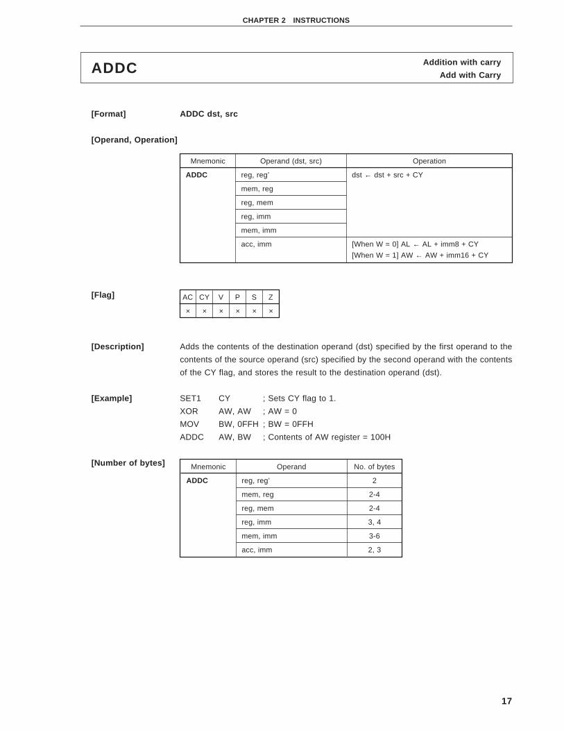
Addition with carryADDC Add with Carry
[Format] ADDC dst, src
[Operand, Operation]
[Flag]
[Description] Adds the contents of the destination operand (dst) specified by the first operand to the
contents of the source operand (src) specified by the second operand with the contents
of the CY flag, and stores the result to the destination operand (dst).
[Example] SET1 CY ; Sets CY flag to 1.
XOR AW, AW ; AW = 0
MOV BW, 0FFH ; BW = 0FFH
ADDC AW, BW ; Contents of AW register = 100H
[Number of bytes]
Mnemonic Operand (dst, src) Operation
ADDC reg, reg’ dst ← dst + src + CY
mem, reg
reg, mem
reg, imm
mem, imm
acc, imm [When W = 0] AL ← AL + imm8 + CY
[When W = 1] AW ← AW + imm16 + CY
AC CY V P S Z
× × × × × ×
Mnemonic Operand No. of bytes
ADDC reg, reg’ 2
mem, reg 2-4
reg, mem 2-4
reg, imm 3, 4
mem, imm 3-6
acc, imm 2, 3

18
CHAPTER 2 INSTRUCTIONS
[Word format]Mnemonic Operand
Operation code
7 6 5 4 3 2 1 0 7 6 5 4 3 2 1 0
ADDC reg, reg’ 0 0 0 1 0 0 1 W 1 1 reg reg‘
mem, reg 0 0 0 1 0 0 0 W mod reg mem
(disp-low) (disp-high)
reg, mem 0 0 0 1 0 0 1 W mod reg mem
(disp-low) (disp-high)
reg, imm 1 0 0 0 0 0 s W 1 1 0 1 0 reg
imm8 or imm16-low imm16-high
mem, imm 1 0 0 0 0 0 s W mod 0 1 0 mem
(disp-low) (disp-high)
imm8 or imm16-low imm16-high
acc, imm 0 0 0 1 0 1 0 W imm8 or imm16-low
imm16-high —

19
CHAPTER 2 INSTRUCTIONS
Packed decimal adjustment of result of additionADJ4AAdjust Nibble Add
[Format] ADJ4A
[Operation] Where AL ^ 0FH > 9 or AC = 1,
AL ← AL + 6
AC ← 1
Where AL > 9FH or CY = 1
AL ← AL + 60H
CY ← 1
[Operand]
[Flag]
[Description] Adjusts the contents of the AL register resulting from addition of two packed decimal
numbers into one packed decimal number.
[Example] ADJ4A
[Number of bytes] 1
[Word format]
Mnemonic Operand
ADJ4A None
AC CY V P S Z
× × U × × ×
Mnemonic OperandOperation code
7 6 5 4 3 2 1 0
ADJ4A None 0 0 1 0 0 1 1 1
20
CHAPTER 2 INSTRUCTIONS
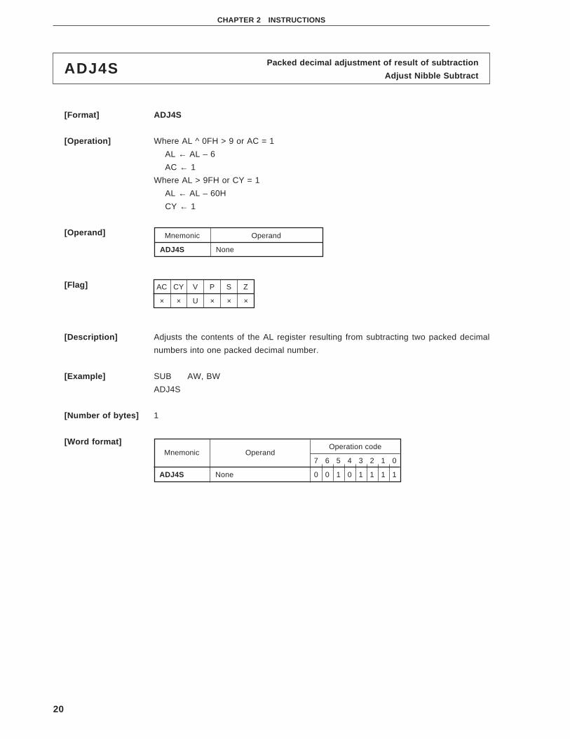
Packed decimal adjustment of result of subtractionADJ4SAdjust Nibble Subtract
[Format] ADJ4S
[Operation] Where AL ^ 0FH > 9 or AC = 1
AL ← AL – 6
AC ← 1
Where AL > 9FH or CY = 1
AL ← AL – 60H
CY ← 1
[Operand]
[Flag]
[Description] Adjusts the contents of the AL register resulting from subtracting two packed decimal
numbers into one packed decimal number.
[Example] SUB AW, BW
ADJ4S
[Number of bytes] 1
[Word format]
Mnemonic Operand
ADJ4S None
AC CY V P S Z
× × U × × ×
Mnemonic OperandOperation code
7 6 5 4 3 2 1 0
ADJ4S None 0 0 1 0 1 1 1 1

21
CHAPTER 2 INSTRUCTIONS
Unpacked decimal adjustment of result of additionADJBAAdjust Byte Add
[Format] ADJBA
[Operation] Where AL ^ 0FH > 9 or AC = 1
AL ← AL + 6
AH ← AH + 1
AC ← 1
CY ← AC
AL ← AL ^ 0FH
[Operand]
[Flag]
[Description] Adjusts the contents of the AL register resulting from adding two unpacked decimal
numbers into one unpacked decimal number. The high-order 4 bits become 0.
[Example] ADJBA
[Number of bytes] 1
[Word format]
Mnemonic Operand
ADJBA None
AC CY V P S Z
× × U U U U
Mnemonic OperandOperation code
7 6 5 4 3 2 1 0
ADJBA None 0 0 1 1 0 1 1 1

22
CHAPTER 2 INSTRUCTIONS
Unpacked decimal adjustment of result of subtractionADJBSAdjust Byte Subtract
[Format] ADJBS
[Operation] Where AL ^ 0FH > 9 or AC = 1
AL ← AL – 6
AH ← AH – 1
AC ← 1
CY ← AC
AL ← AL ^ 0FH
[Operand]
[Flag]
[Description] Adjusts the contents of the AL register resulting from subtracting two unpacked decimal
numbers into one unpacked decimal number. The high-order 4-bits become 0.
[Example] SUB AW, BW
ADJBS
[Number of bytes] 1
[Word format]
Mnemonic Operand
ADJBS None
AC CY V P S Z
× × U U U U
Mnemonic OperandOperation code
7 6 5 4 3 2 1 0
ADJBS None 0 0 1 1 1 1 1 1
23
CHAPTER 2 INSTRUCTIONS
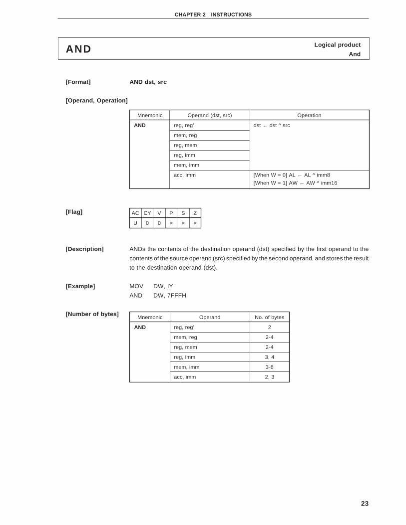
Logical productAND And
[Format] AND dst, src
[Operand, Operation]
[Flag]
[Description] ANDs the contents of the destination operand (dst) specified by the first operand to the
contents of the source operand (src) specified by the second operand, and stores the result
to the destination operand (dst).
[Example] MOV DW, IY
AND DW, 7FFFH
[Number of bytes]
Mnemonic Operand (dst, src) Operation
AND reg, reg’ dst ← dst ^ src
mem, reg
reg, mem
reg, imm
mem, imm
acc, imm [When W = 0] AL ← AL ^ imm8
[When W = 1] AW ← AW ^ imm16
AC CY V P S Z
U 0 0 × × ×
Mnemonic Operand No. of bytes
AND reg, reg’ 2
mem, reg 2-4
reg, mem 2-4
reg, imm 3, 4
mem, imm 3-6
acc, imm 2, 3

24
CHAPTER 2 INSTRUCTIONS
[Word format]
Note The following code may be created depending on the assembler or compiler used.
Even in this case, the instruction is executed normally. Note, however, that some emulators do not support
the functions to disassemble and assemble this instruction.
Mnemonic OperandOperation code
7 6 5 4 3 2 1 0 7 6 5 4 3 2 1 0
AND reg, reg’ 0 0 1 0 0 0 1 W 1 1 reg reg‘
mem, reg 0 0 1 0 0 0 0 W mod reg mem
(disp-low) (disp-high)
reg, mem 0 0 1 0 0 0 1 W mod reg mem
(disp-low) (disp-high)
reg, immNote 1 0 0 0 0 0 0 W 1 1 1 0 0 reg
imm8 or imm16-low imm16-high
mem, imm 1 0 0 0 0 0 0 W mod 1 0 0 mem
(disp-low) (disp-high)
imm8 or imm16-low imm16-high
acc, imm 0 0 1 0 0 1 0 W imm8 or imm16-low
imm16-high —
7 6 5 4 3 2 1 0 7 6 5 4 3 2 1 0
1 0 0 0 0 0 1 W 1 1 1 0 0 reg
imm8 –

25
CHAPTER 2 INSTRUCTIONS
Conditional branch where CY = 1BCBranch if Carry
BL Branch if Lower
[Format] BC short-label
BL short-label
[Operation] Where CY = 1: PC ← PC + ext-disp8
[Operand]
[Flag]
[Description] Loads the current PC value with an 8-bit displacement added (actually, sign-extended 16
bits) to the PC when the CY flag is 1.
Execution can be branched in a segment where this instruction is placed and in an address
range of –128 to +127 bytes.
[Example] TEST AL, BL
BC SHORT LP4 ; LP4 = label
TEST AL, BL
BL SHORT LP5 ; LP5 = label
LP4:
[Number of bytes] 2
[Word format]
Mnemonic Operand
BC short-label
BL
AC CY V P S Z
...
...
Mnemonic OperandOperation code
7 6 5 4 3 2 1 0 7 6 5 4 3 2 1 0
BC short-label 0 1 1 1 0 0 1 0 disp8
BL
26
CHAPTER 2 INSTRUCTIONS
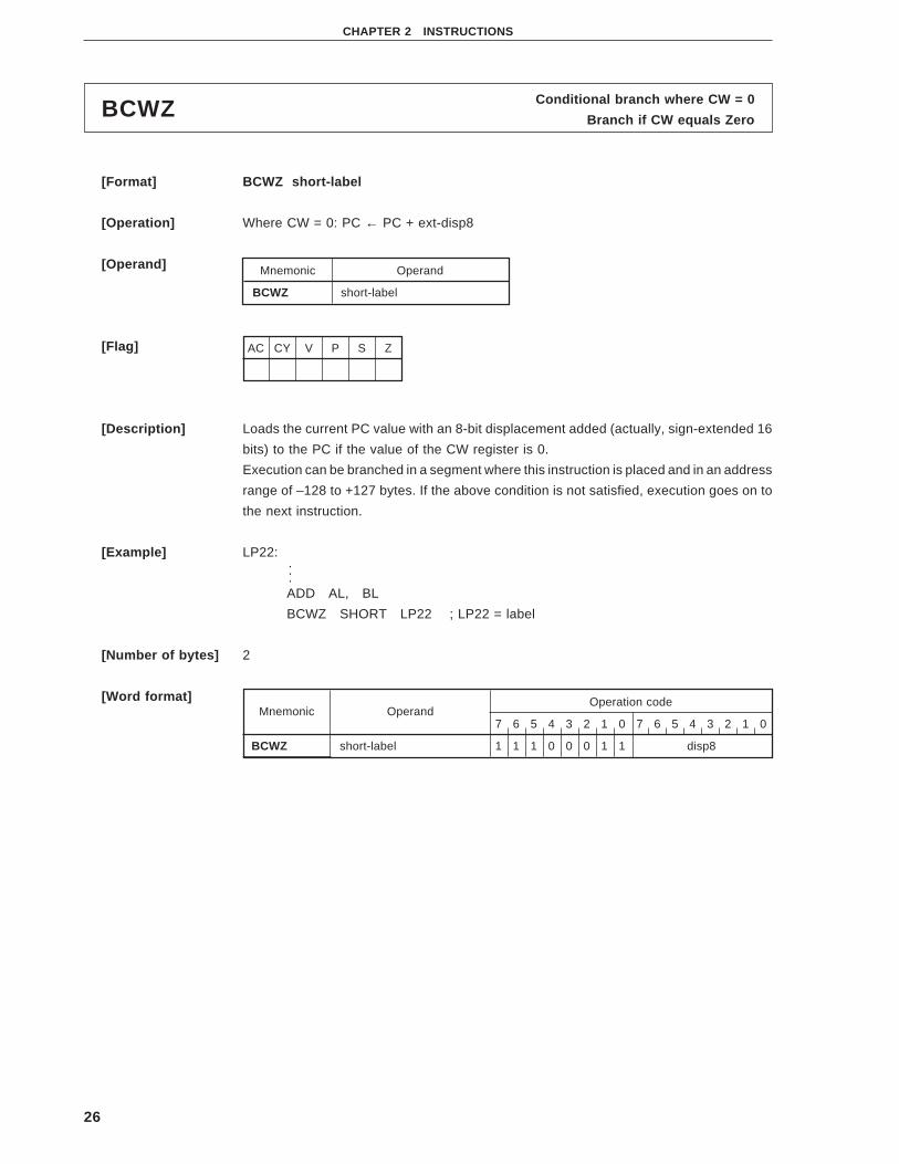
Conditional branch where CW = 0BCWZ Branch if CW equals Zero
[Format] BCWZ short-label
[Operation] Where CW = 0: PC ← PC + ext-disp8
[Operand]
[Flag]
[Description] Loads the current PC value with an 8-bit displacement added (actually, sign-extended 16
bits) to the PC if the value of the CW register is 0.
Execution can be branched in a segment where this instruction is placed and in an address
range of –128 to +127 bytes. If the above condition is not satisfied, execution goes on to
the next instruction.
[Example] LP22:
ADD AL, BL
BCWZ SHORT LP22 ; LP22 = label
[Number of bytes] 2
[Word format]Mnemonic Operand
Operation code
7 6 5 4 3 2 1 0 7 6 5 4 3 2 1 0
BCWZ short-label 1 1 1 0 0 0 1 1 disp8
Mnemonic Operand
BCWZ short-label
AC CY V P S Z
...
27
CHAPTER 2 INSTRUCTIONS
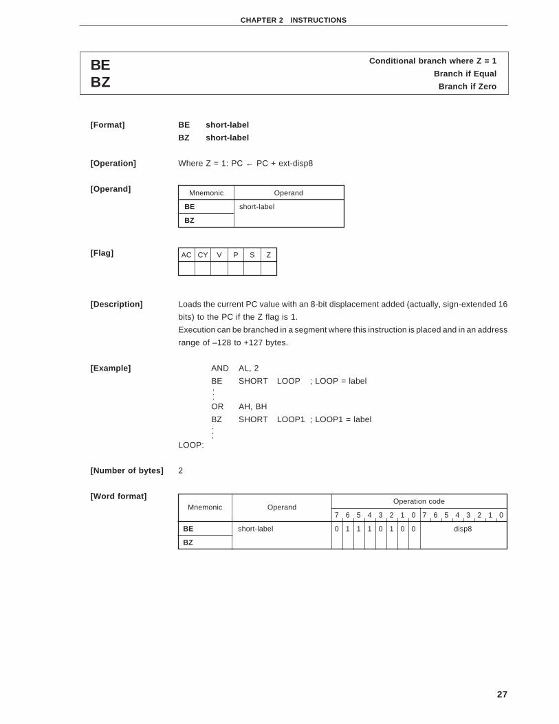
Conditional branch where Z = 1BEBranch if Equal
BZ Branch if Zero
[Format] BE short-label
BZ short-label
[Operation] Where Z = 1: PC ← PC + ext-disp8
[Operand]
[Flag]
[Description] Loads the current PC value with an 8-bit displacement added (actually, sign-extended 16
bits) to the PC if the Z flag is 1.
Execution can be branched in a segment where this instruction is placed and in an address
range of –128 to +127 bytes.
[Example] AND AL, 2
BE SHORT LOOP ; LOOP = label
OR AH, BH
BZ SHORT LOOP1 ; LOOP1 = label
LOOP:
[Number of bytes] 2
[Word format]
Mnemonic Operand
BE short-label
BZ
AC CY V P S Z
...
...
Mnemonic OperandOperation code
7 6 5 4 3 2 1 0 7 6 5 4 3 2 1 0
BE short-label 0 1 1 1 0 1 0 0 disp8
BZ

28
CHAPTER 2 INSTRUCTIONS
Conditional branch where S v V = 0BGEBranch if Greater Than or Equal
[Format] BGE short-label
[Operation] Where S v V = 0: PC ← PC + ext-disp8
[Operand]
[Flag]
[Description] Loads the current PC value with an 8-bit displacement added (actually, sign-extended 16
bits) to the PC if the result of exclusive OR (XOR) between the S and V flags is 0.
Execution can be branched in a segment where this instruction is placed and in an address
range of –128 to +127 bytes.
Execution goes on to the next instruction if the above condition is not satisfied.
[Example] SHL AL, 1
BGE SHORT LP16 ; LP16 = label
LP16:
[Number of bytes] 2
[Word format]
Mnemonic Operand
BGE short-label
AC CY V P S Z
...
Mnemonic OperandOperation code
7 6 5 4 3 2 1 0 7 6 5 4 3 2 1 0
BGE short-label 0 1 1 1 1 1 0 1 disp8

29
CHAPTER 2 INSTRUCTIONS
Conditional branch where (S v V) v Z = 0BGT Branch if Greater Than
[Format] BGT short-label
[Operation] (S v V) v Z = 0: PC ← PC + ext-disp8
[Operand]
[Flag]
[Description] Loads the current PC value with an 8-bit displacement added (actually, sign-extended 16
bits) to the PC if the result of ORing between the result of exclusive OR (XOR) of the S
and V flags, and the Z flag is 0.
Execution can be branched in a segment where this instruction is placed and in an address
range of –128 to +127 bytes.
Execution goes on to the next instruction if the above condition is not satisfied.
[Example] LP18:
SHL AL, 1
BGT LP18
[Number of bytes] 2
[Word format]
Mnemonic Operand
BGT short-label
AC CY V P S Z
...
Mnemonic OperandOperation code
7 6 5 4 3 2 1 0 7 6 5 4 3 2 1 0
BGT short-label 0 1 1 1 1 1 1 1 disp8

30
CHAPTER 2 INSTRUCTIONS
Conditional branch where CY v Z = 0BH Branch if Higher
[Format] BH short-label
[Operation] Where CY v Z = 0: PC ← PC + ext-disp8
[Operand]
[Flag]
[Description] Loads the current PC value with an 8-bit displacement added (actually, sign-extended 16
bits) to the PC if the result of ORing the CY and Z flags is 0.
Execution can be branched in a segment where this instruction is placed and in an address
range of –128 to +127 bytes.
[Example] ROL AL, 1
BH SHORT LP10 ; LP10 = label
LP10:
[Number of bytes] 2
[Word format]
Mnemonic Operand
BH short-label
AC CY V P S Z
...
Mnemonic OperandOperation code
7 6 5 4 3 2 1 0 7 6 5 4 3 2 1 0
BH short-label 0 1 1 1 0 1 1 1 disp8

31
CHAPTER 2 INSTRUCTIONS
Conditional branch where (S v V) v Z = 1BLE Branch if Less than or Equal
[Format] BLE short-label
[Operation] (S v V) v Z = 1: PC ← PC + ext-disp8
[Operand]
[Flag]
[Description] Loads the current PC value with an 8-bit displacement added (actually, sign-extended 16
bits) to the PC if the result of ORing between the result of exclusive OR (XOR) of the S
and V flags, and the Z flag is 1.
Execution can be branched in a segment where this instruction is placed and in an address
range of –128 to +127 bytes.
Execution goes on to the next instruction if the above condition is not satisfied.
[Example] LP17:
SHR AL, 1
BLE SHORT LP17
[Number of bytes] 2
[Word format]
Mnemonic Operand
BLE short-label
AC CY V P S Z
...
Mnemonic OperandOperation code
7 6 5 4 3 2 1 0 7 6 5 4 3 2 1 0
BLE short-label 0 1 1 1 1 1 1 0 disp8

32
CHAPTER 2 INSTRUCTIONS
Conditional branch where S v V = 1BLT Branch if Less Than
[Format] BLT short-label
[Operation] Where S v V = 1: PC ← PC + ext-disp8
[Operand]
[Flag]
[Description] Loads the current PC value with an 8-bit displacement added (actually, sign-extended 16
bits) to the PC if the result of exclusive OR between the S and Z flags is 1.
Execution can be branched in a segment where this instruction is placed and in an address
range of –128 to +127 bytes.
Execution goes on to the next instruction if the above condition is not satisfied.
[Example] ADD AL, BL
BLT SHORT LP15 ; LP15 = label
LP15:
[Number of bytes] 2
[Word format]
Mnemonic Operand
BLT short-label
AC CY V P S Z
...
Mnemonic OperandOperation code
7 6 5 4 3 2 1 0 7 6 5 4 3 2 1 0
BLT short-label 0 1 1 1 1 1 0 0 disp8
33
CHAPTER 2 INSTRUCTIONS
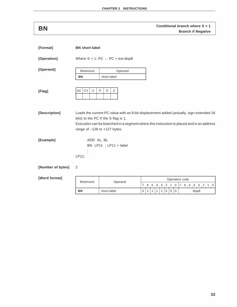
Conditional branch where S = 1BNBranch if Negative
[Format] BN short-label
[Operation] Where S = 1: PC ← PC + ext-disp8
[Operand]
[Flag]
[Description] Loads the current PC value with an 8-bit displacement added (actually, sign-extended 16
bits) to the PC if the S flag is 1.
Execution can be branched in a segment where this instruction is placed and in an address
range of –128 to +127 bytes.
[Example] ADD AL, BL
BN LP11 ; LP11 = label
LP11:
[Number of bytes] 2
[Word format]
Mnemonic Operand
BN short-label
AC CY V P S Z
...
Mnemonic OperandOperation code
7 6 5 4 3 2 1 0 7 6 5 4 3 2 1 0
BN short-label 0 1 1 1 1 0 0 0 disp8

34
CHAPTER 2 INSTRUCTIONS
Conditional branch where CY = 0BNCBranch if Not Carry
BNL Branch if Not Lower
[Format] BNC short-label
BNL short-label
[Operation] Where CY = 0: PC ← PC + ext-disp8
[Operand]
[Flag]
[Description] Loads the current PC value with an 8-bit displacement added (actually, sign-extended 16
bits) to the PC if the CY flag is 0.
Execution can be branched in a segment where this instruction is placed and in an address
range of –128 to +127 bytes.
[Example] ROR AL, 1
BNC SHORT LP6 ; LP6 = label
ROR AL, 1
BNL SHORT LP7 ; LP7 = label
LP6:
[Number of bytes] 2
[Word format]
Mnemonic Operand
BNC short-label
BNL
AC CY V P S Z
Mnemonic OperandOperation code
7 6 5 4 3 2 1 0 7 6 5 4 3 2 1 0
BNC short-label 0 1 1 1 0 0 1 1 disp8
BNL
...
...

35
CHAPTER 2 INSTRUCTIONS
Conditional branch where Z = 0BNEBranch if Not Equal
BNZ Branch if Not Zero
[Format] BNE short-label
BNZ short-label
[Operation] Where Z = 0: PC ← PC + ext-disp8
[Operand]
[Flag]
[Description] Loads the current PC value with an 8-bit displacement added (actually, sign-extended 16
bits) to the PC if the Z flag is 0.
Execution can be branched in a segment where this instruction is placed and in an address
range of –128 to +127 bytes.
[Example] OR AL, BL
BNE SHORT LP8 ; LP8 = label
AND SH, BH
BNZ SHORT LP9 ; LP9 = label
LP8:
[Number of bytes] 2
[Word format]
Mnemonic Operand
BNE short-label
BNZ
AC CY V P S Z
...
...
Mnemonic OperandOperation code
7 6 5 4 3 2 1 0 7 6 5 4 3 2 1 0
BNE short-label 0 1 1 1 0 1 0 1 disp8
BNZ
36
CHAPTER 2 INSTRUCTIONS
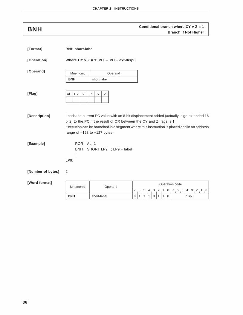
Conditional branch where CY v Z = 1BNHBranch if Not Higher
[Format] BNH short-label
[Operation] Where CY v Z = 1: PC ← PC + ext-disp8
[Operand]
[Flag]
[Description] Loads the current PC value with an 8-bit displacement added (actually, sign-extended 16
bits) to the PC if the result of OR between the CY and Z flags is 1.
Execution can be branched in a segment where this instruction is placed and in an address
range of –128 to +127 bytes.
[Example] ROR AL, 1
BNH SHORT LP9 ; LP9 = label
LP9:
[Number of bytes] 2
[Word format]
Mnemonic Operand
BNH short-label
AC CY V P S Z
...
Mnemonic OperandOperation code
7 6 5 4 3 2 1 0 7 6 5 4 3 2 1 0
BNH short-label 0 1 1 1 0 1 1 0 disp8

37
CHAPTER 2 INSTRUCTIONS
Conditional branch where V = 0BNV Branch if not Overflow
[Format] BNV short-label
[Operation] Where V = 0: PC ← PC + ext-disp8
[Operand]
[Flag]
[Description] Loads the current PC value with an 8-bit displacement added (actually, sign-extended 16
bits) to the PC if the V flag is 0.
Execution can be branched in a segment where this instruction is placed and in an address
range of –128 to +127 bytes.
[Example] ROR AL, 1
BNV LP3
LP3:
[Number of bytes] 2
[Word format]
Mnemonic Operand
BNV short-label
Mnemonic OperandOperation code
7 6 5 4 3 2 1 0 7 6 5 4 3 2 1 0
BNV short-label 0 1 1 1 0 0 0 1 disp8
AC CY V P S Z
...
38
CHAPTER 2 INSTRUCTIONS
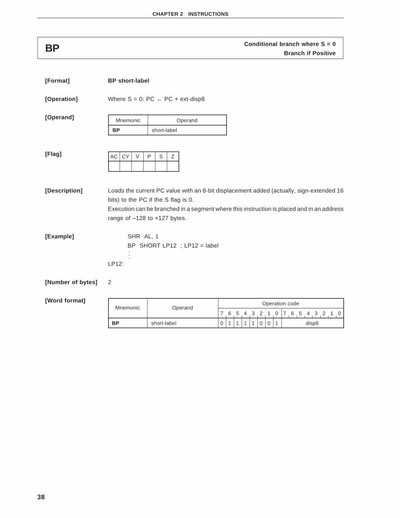
Conditional branch where S = 0BPBranch if Positive
[Format] BP short-label
[Operation] Where S = 0: PC ← PC + ext-disp8
[Operand]
[Flag]
[Description] Loads the current PC value with an 8-bit displacement added (actually, sign-extended 16
bits) to the PC if the S flag is 0.
Execution can be branched in a segment where this instruction is placed and in an address
range of –128 to +127 bytes.
[Example] SHR AL, 1
BP SHORT LP12 ; LP12 = label
LP12:
[Number of bytes] 2
[Word format]
Mnemonic Operand
BP short-label
AC CY V P S Z
...
Mnemonic OperandOperation code
7 6 5 4 3 2 1 0 7 6 5 4 3 2 1 0
BP short-label 0 1 1 1 1 0 0 1 disp8

39
CHAPTER 2 INSTRUCTIONS
Conditional branch where P = 1BPEBranch if Parity Even
[Format] BPE short-label
[Operation] Where P = 1: PC ← PC + ext-disp8
[Operand]
[Flag]
[Description] Loads the current PC value with an 8-bit displacement added (actually, sign-extended 16
bits) to the PC if the P flag is 1.
Execution can be branched in a segment where this instruction is placed and in an address
range of –128 to +127 bytes.
[Example] ADD AL, BL
BPE SHORT LP13 ; LP13 = label
LP13:
[Number of bytes] 2
[Word format]
Mnemonic Operand
BPE short-label
AC CY V P S Z
...
Mnemonic OperandOperation code
7 6 5 4 3 2 1 0 7 6 5 4 3 2 1 0
BPE short-label 0 1 1 1 1 0 1 0 disp8

40
CHAPTER 2 INSTRUCTIONS
Conditional branch where P = 0BPO Branch if Parity Odd
[Format] BPO short-label
[Operation] Where P = 0: PC ← PC + ext-disp8
[Operand]
[Flag]
[Description] Loads the current PC value with an 8-bit displacement added (actually, sign-extended 16
bits) to the PC if the P flag is 0.
Execution can be branched in a segment where this instruction is placed and in an address
range of –128 to +127 bytes.
[Example] ADD AL, BL
BPO SHORT LP14 ; LP14 = label
LP14:
[Number of bytes] 2
[Word format]Mnemonic Operand
Operation code
7 6 5 4 3 2 1 0 7 6 5 4 3 2 1 0
BPO short-label 0 1 1 1 1 0 1 1 disp8
Mnemonic Operand
BPO short-label
AC CY V P S Z
...

41
CHAPTER 2 INSTRUCTIONS
Unconditional branchBR Branch
[Format] BR target
[Operation, operand]
[Flag]
[Description] • When target = near-label
Transfers the current PC value with a 16-bit displacement (disp) added to the PC.
If the branch address is within a segment where this instruction is placed, the assembler
automatically executes this instruction.
• When target = short-label
Transfers the current PC value with an 8-bit displacement added (actually, sign-
extended 16 bits (ext-disp8)) to the PC.
If the branch address is within a segment where this instruction is placed, and within
a range of ±127 bytes, the assembler automatically executes this instruction.
• When target = regptr16 or target = memptr16
Transfers the contents of the target operand (target) to the PC. Execution can branch
to any address in the segment where this instruction is placed.
• When target = far-label
Transfers the 16-bit offset data at the second and third byte positions of the instruction
to the PC, and the 16-bit segment data at the fourth and fifth byte position of the
instruction to the PS.
Execution can branch to any address of any segment.
• When target = memptr32
Loads the high-order 2 bytes of a 32-bit memory area to the PS, and the low-order 2
bytes, to the PC.
Execution can branch to any address of any segment.
Mnemonic Operand (target) Operation
BR near-label PC ← PC + disp
short-label PC ← PC + ext-disp8
regptr16PC ← target
memptr16
far-label PS ← seg
PC ← offset
memptr32 PS ← (memptr32 + 3, memptr32 + 2)
PC ← (memptr32 + 1, memptr32)
AC CY V P S Z
42
CHAPTER 2 INSTRUCTIONS
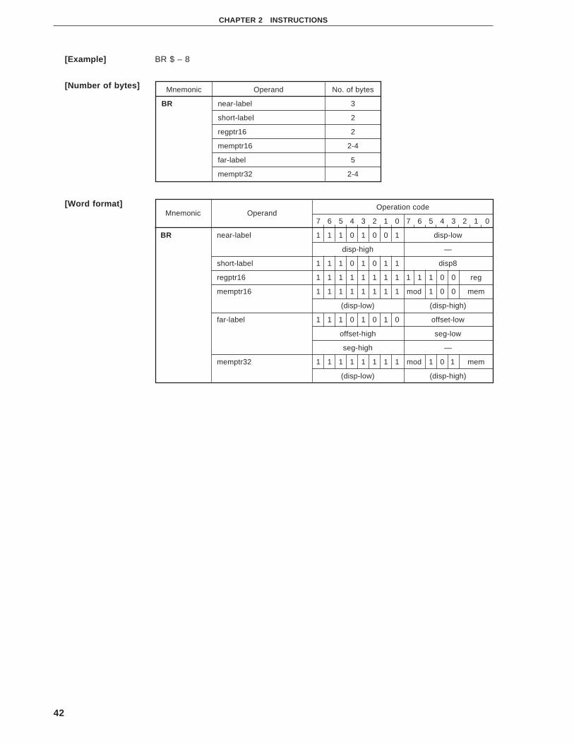
[Example] BR $ – 8
[Number of bytes]
[Word format]
Mnemonic Operand No. of bytes
BR near-label 3
short-label 2
regptr16 2
memptr16 2-4
far-label 5
memptr32 2-4
Mnemonic OperandOperation code
7 6 5 4 3 2 1 0 7 6 5 4 3 2 1 0
BR near-label 1 1 1 0 1 0 0 1 disp-low
disp-high —
short-label 1 1 1 0 1 0 1 1 disp8
regptr16 1 1 1 1 1 1 1 1 1 1 1 0 0 reg
memptr16 1 1 1 1 1 1 1 1 mod 1 0 0 mem
(disp-low) (disp-high)
far-label 1 1 1 0 1 0 1 0 offset-low
offset-high seg-low
seg-high —
memptr32 1 1 1 1 1 1 1 1 mod 1 0 1 mem
(disp-low) (disp-high)

43
CHAPTER 2 INSTRUCTIONS
Software trapBRK Break
[Format] BRK target
[Operand, operation]
[Flag]
[Description] Saves the values of PSW, PS, and PC to the stack and resets the IE and BRK flags to 0.
Then loads the low-order 2 bytes of vector 3 in the interrupt vector table to the PC, and
the high-order 2 bytes to the PS if target = 3.
If target = imm8, loads the low-order 2 bytes of the interrupt vector table (4 bits) specified
by the 8-bit immediate data to the PC, and the high-order 2 bytes to the PS.
[Example] • BRK 3
• BRK 5
[Number of bytes]
[Word format]
Mnemonic Operand (target) Operation
BRK 3 TA ← (00DH, 00CH)
TC ← (00FH, 00EH)
SP ← SP – 2, (SP + 1, SP) ← PSW
IE ← 0, BRK ← 0
SP ← SP – 2, (SP + 1, SP) ← PS
PS ← TC
SP ← SP – 2, (SP + 1, SP) ← PC
PC ← TA
imm8 (≠ 3) TA ← (imm8 × 4 + 1, imm8 × 4)
TC ← (imm8 × 4 + 3, imm8 × 4 + 2)
SP ← SP – 2, (SP + 1, SP) ← PSW
IE ← 0, BRK ← 0
SP ← SP – 2, (SP + 1, SP) ← PS
PS ← TC
SP ← SP – 2, (SP + 1, SP) ← PC
PC ← TA
AC CY V P S Z IE BRK
0 0
Mnemonic Operand No. of bytes
BRK 3 1
imm8 2
Mnemonic OperandOperation code
7 6 5 4 3 2 1 0 7 6 5 4 3 2 1 0
BRK 3 1 1 0 0 1 1 0 0 —
imm8 1 1 0 0 1 1 0 1 imm8

44
CHAPTER 2 INSTRUCTIONS
Starts emulation modeBRKEM [except V33A and V53A]Break for Emulation
[Format] BRKEM imm8
[Operation] TA ← (imm8 × 4 + 1, imm8 × 4)
TC ← (imm8 × 4 + 3, imm8 × 4 + 2)
SP ← SP – 2, (SP + 1, SP) ← PSW
MD ← 0: Write enable status
SP ← SP – 2, (SP + 1, SP) ← PS
PS ← TC
SP ← SP – 2, (SP + 1, SP) ← PC
PC ← TA
[Operand]
[Flag]
[Description] This instruction starts the emulation mode. The values of the PSW, PS, and PC are saved
to the stack, the MD flag is reset to 0 to enable writing, and execution jumps to the emulation
address specified by the interrupt vector specified by the 8-bit immediate data described
as an operand.
When the instruction code of the interrupt service routine (for emulation) to which execution
has jumped is fetched, the CPU interprets this code as an instruction of the µPD8080AF
and executes. To return to the native mode from the emulation mode, use the RETEM or
CALLN instruction.
[Example] BRKEM 40H
[Number of bytes] 3
[Word format]
Mnemonic Operand
BRKEM imm8
AC CY V P S Z MD
0
Mnemonic OperandOperation code
7 6 5 4 3 2 1 0 7 6 5 4 3 2 1 0
BRKEM imm8 0 0 0 0 1 1 1 1 1 1 1 1 1 1 1 1
imm8 —

45
CHAPTER 2 INSTRUCTIONS
Overflow exceptionBRKVBreak if Overflow
[Format] BRKV
[Operation] Where V = 1, TA ← (011H, 010H)
TC ← (013H, 012H)
SP ← SP – 2, (SP + 1, SP) ← PSW
IE ← 0, BRK ← 0
SP ← SP – 2, (SP + 1, SP) ← PS
PS ← TC
SP ← SP – 2, (SP + 1, SP) ← PC
PC ← TA
[Operand]
[Flag]
[Description] Saves the values of PSW, PS, and PC to the stack and resets the IE and BRK flags to 0
if the V flag is set to 1. Then loads the low-order 2 bytes of vector 4 of the interrupt vector
table to the PC and the high-order 2 bytes to the PS if target = 3.
Execution proceeds to the next instruction if the V flag is reset to 0.
[Example] BRKV
[Number of bytes] 1
[Word format]
Mnemonic Operand
BRKV None
AC CY V P S Z IE BRK
0 0
Mnemonic OperandOperation code
7 6 5 4 3 2 1 0
BRKV None 1 1 0 0 1 1 1 0
46
CHAPTER 2 INSTRUCTIONS
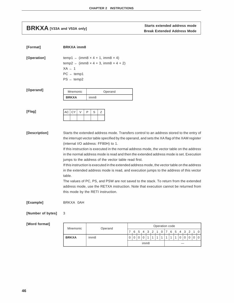
Starts extended address modeBRKXA [V33A and V53A only]Break Extended Address Mode
[Format] BRKXA imm8
[Operation] temp1 ← (imm8 × 4 + 1, imm8 × 4)
temp2 ← (imm8 × 4 + 3, imm8 × 4 + 2)
XA ← 1
PC ← temp1
PS ← temp2
[Operand]
[Flag]
[Description] Starts the extended address mode. Transfers control to an address stored to the entry of
the interrupt vector table specified by the operand, and sets the XA flag of the XAM register
(internal I/O address: FF80H) to 1.
If this instruction is executed in the normal address mode, the vector table on the address
in the normal address mode is read and then the extended address mode is set. Execution
jumps to the address of the vector table read first.
If this instruction is executed in the extended address mode, the vector table on the address
in the extended address mode is read, and execution jumps to the address of this vector
table.
The values of PC, PS, and PSW are not saved to the stack. To return from the extended
address mode, use the RETXA instruction. Note that execution cannot be returned from
this mode by the RETI instruction.
[Example] BRKXA 0AH
[Number of bytes] 3
[Word format]
Mnemonic Operand
BRKXA imm8
AC CY V P S Z
Mnemonic OperandOperation code
7 6 5 4 3 2 1 0 7 6 5 4 3 2 1 0
BRKXA imm8 0 0 0 0 1 1 1 1 1 1 1 0 0 0 0 0
imm8 —

47
CHAPTER 2 INSTRUCTIONS
Bus lock prefixBUSLOCK Bus Lock Prefix
[Format] BUSLOCK
[Operation] Bus Lock Prefix
[Operand]
[Flag]
[Description] • V20, V30, V20H, and V30HL
In large-scale mode : Outputs the bus lock signal (BUSLOCK) while the single instruction
following this instruction is executed. If this instruction is used
for a block processing instruction with a repeat prefix, the BUSLOCK
signal is continuously output until the block processing is completed.
In small-scale mode: Although the BUSLOCK signal is not output, the bus hold request
is disabled while the BUSLOCK signal is output in the large-scale
mode. Therefore, this instruction is useful for not accepting the
bus hold request during block processing.
Cautions 1. Do not place this instruction immediately before the POLL instruction.
2. The hardware interrupt requests (NMI and INT) and single-step break
are not accepted between this instruction and the next instruction.
• Other than V20, V30, V20HL, and V30HL
Outputs the bus lock signal (BUSLOCK) while the single instruction following this
instruction is executed.
If this instruction is used for a block processing instruction with a repeat prefix, the
BUSLOCK signal is continuously output until the block processing is completed.
Cautions 1. Do not place this instruction immediately before the POLL instruction.
2. The hardware interrupt requests (maskable interrupt and non- maskable
interrupt) and single-step break are not accepted between this instruction
and the next instruction.
[Example] BUSLOCK REP MOVBKB
[Number of bytes] 1
[Word format]
Mnemonic Operand
BUSLOCK None
AC CY V P S Z
Mnemonic OperandOperation code
7 6 5 4 3 2 1 0
BUSLOCK None 1 1 1 1 0 0 0 0

48
CHAPTER 2 INSTRUCTIONS
Conditional branch where V = 1BVBranch if Overflow
[Format] BV short-label
[Operation] Where V= 1: PC ← PC + ext-disp8
[Operand]
[Flag]
[Description] Loads the current PC value with an 8-bit displacement added (actually, sign-extended 16
bits) to the PC when the V flag is 1.
Execution can be branched in a segment where this instruction is placed and in an address
range of –128 to +127 bytes.
[Example] LP2:
SHL AL, 1
BV SHORT LP2
[Number of bytes] 2
[Word format]
AC CY V P S Z
Mnemonic Operand
BV short-label
...
Mnemonic OperandOperation code
7 6 5 4 3 2 1 0 7 6 5 4 3 2 1 0
BV short-label 0 1 1 1 0 0 0 0 disp8

49
CHAPTER 2 INSTRUCTIONS
Subroutine callCALLCall
[Format] CALL target
[Operand, operation]
[Flag]
[Description] • When target = near-proc or target = regptr16
Saves the value of the PC to the stack and then transfers the next contents of the target
operand (target) to the PC.
When target = near-proc : 16-bit relative address
When target = regptr16 : Value of 16-bit register (offset)
• When target = memptr16
Saves the value of the PC to the stack and then transfers the contents of a 16-bit memory
area (offset) addressed by the target operand (target) to the PC.
Any address in the segment where this instruction is placed can be called.
Mnemonic Operand (target) Operation
CALL near-proc SP ← SP – 2
(SP + 1, SP) ← PC
PC ← PC + disp
regptr16 SP ← SP – 2
(SP + 1, SP) ← PC
PC ← regptr16
memptr16 TA ← (memptr16 + 1, memptr16)
SP ← SP – 2
(SP + 1, SP) ← PC
PC ← TA
far-proc SP ← SP – 2
(SP + 1, SP) ← PS
PS ← seg
SP ← SP – 2
(SP + 1, SP) ← PC
PS ← offset
memptr32 TA ← (memptr32 + 1, memptr32)
TB ← (memptr32 + 3, memptr32 + 2)
SP ← SP – 2
(SP + 1, SP) ← PS
PS ← TB
SP ← SP – 2
(SP + 1, SP) ← PC
PC ← TA
AC CY V P S Z

50
CHAPTER 2 INSTRUCTIONS
• When target = far-proc
Saves the values of PC and PS to the stack and transfers the second and third bytes
of the instruction to the PC, and the fourth and fifth bytes to the PS.
This instruction can call any address in any segment.
• When target = memptr32
Saves the values of PC and PS to the stack and transfers the high-order 2 bytes of a
32-bit memory area addressed by the target operand (target) to the PS and the low-
order 2 bytes to the PC.
This instruction can call any address in any segment.
[Example] • CALL $ + 10
• CALL SUB1 ; SUB1 is label
[Number of bytes]
[Word format]
Mnemonic Operand No. of bytes
CALL near-proc 3
regptr16 2
memptr16 2-4
far-proc 5
memptr32 2-4
Mnemonic OperandOperation code
7 6 5 4 3 2 1 0 7 6 5 4 3 2 1 0
CALL near-proc 1 1 1 0 1 0 0 0 disp-low
disp-high —
regptr16 1 1 1 1 1 1 1 1 1 1 0 1 0 reg
memptr16 1 1 1 1 1 1 1 1 mod 0 1 0 mem
(disp-low) (disp-high)
far-proc 1 0 0 1 1 0 1 0 offset-low
offset-high seg-low
seg-high —
memptr32 1 1 1 1 1 1 1 1 mod 0 1 1 mem
(disp-low) (disp-high)

51
CHAPTER 2 INSTRUCTIONS
Native mode callCALLN [except V33A and V53A]Call Native
[Format] CALLN imm8
[Operation] TA ← (imm8 × 4 + 1, imm8 × 4)
TC ← (imm8 × 4 + 3, imm8 × 4 + 2)
SP ← SP – 2, (SP + 1, SP) ← PSW
MD ← 1
SP ← SP – 2, (SP + 1, SP) ← PS
PS ← TC
SP ← SP – 2, (SP + 1, SP) ← PC
PC ← TA
[Operand]
[Flag]
[Description] When this instruction is executed in the emulation mode (this instruction is interpreted as
an instruction of the µPD8080AF), the CPU saves the values of PS, PC, and PSW to the
stack (at this time, MD = 0 is saved), sets the MD flag to 1, and loads an interrupt vector
specified by the 8-bit immediate data described as an operand to the PS and PC.
In this way, an interrupt routine in the native mode can be called from the emulation mode.
To return to the emulation mode from this interrupt routine, use the RETI instruction.
[Example] CALLN 40H
[Number of bytes] 3
[Word format]
AC CY V P S Z MD
1
Mnemonic Operand
CALLN imm8
Mnemonic OperandOperation code
7 6 5 4 3 2 1 0 7 6 5 4 3 2 1 0
CALLN imm8 1 1 1 0 1 1 0 1 1 1 1 0 1 1 0 1
imm8 —

52
CHAPTER 2 INSTRUCTIONS
Index value checkCHKINDCheck Index
[Format] CHKIND reg16, mem32
[Operation] When (mem32) > reg16 or (mem32 + 2) < reg16
TA ← (015H, 014H)
TC ← (017H, 016H)
SP ← SP – 2, (SP + 1, SP) ← PSW
IE ← 0, BRK ← 0
SP ← SP – 2, (SP +1, SP) ← PS
PS ← TC
SP ← SP – 2, (SP + 1, SP) ← PC
PC ← TA
[Operand]
[Flag] If interrupt condition is satisfied
If interrupt condition is not satisfied
[Description] This instruction checks whether an index value that specifies an element is in a defined
area if the data structure is of array type. If the index exceeds the defined area, the BRK
5 instruction is started. The defined area value is set to 2 words in memory in advance (the
first word is the lower-limit value and the second word is the higher-limit value).
As the index value, the register (any 16-bit register) used by an array manipulation program
is used.
Mnemonic Operand
CHKIND reg16, mem32
AC CY V P S Z IE BRK
0 0
AC CY V P S Z IE BRK
����������������
Upper limit
Lower limit
Array element(Upper limit)
(Lower limit)
mem32+2
mem32
15 0
Memory
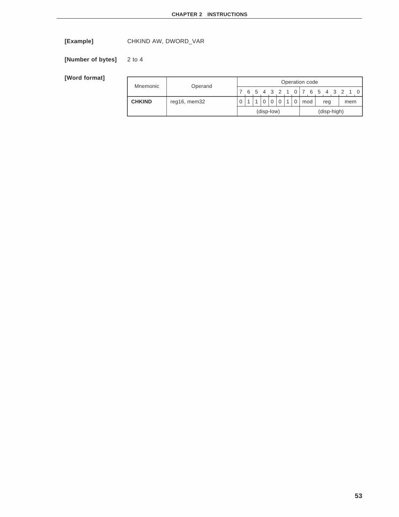
53
CHAPTER 2 INSTRUCTIONS
[Example] CHKIND AW, DWORD_VAR
[Number of bytes] 2 to 4
[Word format]Mnemonic Operand
Operation code
7 6 5 4 3 2 1 0 7 6 5 4 3 2 1 0
CHKIND reg16, mem32 0 1 1 0 0 0 1 0 mod reg mem
(disp-low) (disp-high)

54
CHAPTER 2 INSTRUCTIONS
Resets bitCLR1Clear bit
[Format] (1) CLR1 dst, src
(2) CRL1 dst
[Operation] Format (1): Bit n of dst (n is specified by src) ← 0
Format (2): dst ← 0
[Operand] Format (1) Format (2)
[Flag] Format (1)
Format (2) (when dst = CY)
Format (2) (when dst = DIR)
Mnemonic Operand (dst, src)
CLR1 reg8, CL
mem8, CL
reg16, CL
mem16, CL
reg8, imm3
mem8, imm3
reg16, imm4
mem16, imm4
Mnemonic Operand (dst)
CLR1 CY
DIR
AC CY V P S Z DIR
0
AC CY V P S Z
0
AC CY V P S Z

55
CHAPTER 2 INSTRUCTIONS
[Description] Format (1) : Resets bit n (n is the contents of the source operand (src) specified by the
second operand) of the destination operand (dst) specified by the first
operand, and stores the result to the destination operand (dst).
If the operand is reg8, CL or mem8, CL, only the low-order 3 bits (0 to 7) of
the value of CL are valid.
If the operand is reg16, CL or mem16, CL, only the low-order 4 bits (0 to 15)
of the value of CL are valid.
If the operand is reg8, imm3, only the low-order 3 bits of the immediate data
at the fourth byte position of the instruction are valid.
If the operand is mem8, imm3, only the low-order 3 bits of the immediate data
at the last byte position of the instruction are valid.
If the operand is reg16, imm4, only the low-order 4 bits of the immediate data
at the fourth byte position of the instruction are valid.
If the operand is mem16, imm4, only the low-order 4 bits of the immediate
data at the last byte of the instruction are valid.
Format (2) : Resets the CY flag if dst = CY.
Resets the DIR flag if dst = DIR. Also sets so that the index registers (IX and
IY) are auto-incremented when MOVBK, CMPBK, CMPM, LDM, STM, INM,
or OUTM instruction is executed.
[Example] CLR1 CY
SHL AL,1
BC $ + 6
[Number of bytes] Mnemonic Operand No. of bytes
CLR1 reg8, CL 3
mem8, CL 3-5
reg16, CL 3
mem16, CL 3-5
reg8, imm3 4
mem8, imm3 4-6
reg16, imm4 4
mem16, imm4 4-6
CY 1
DIR 1
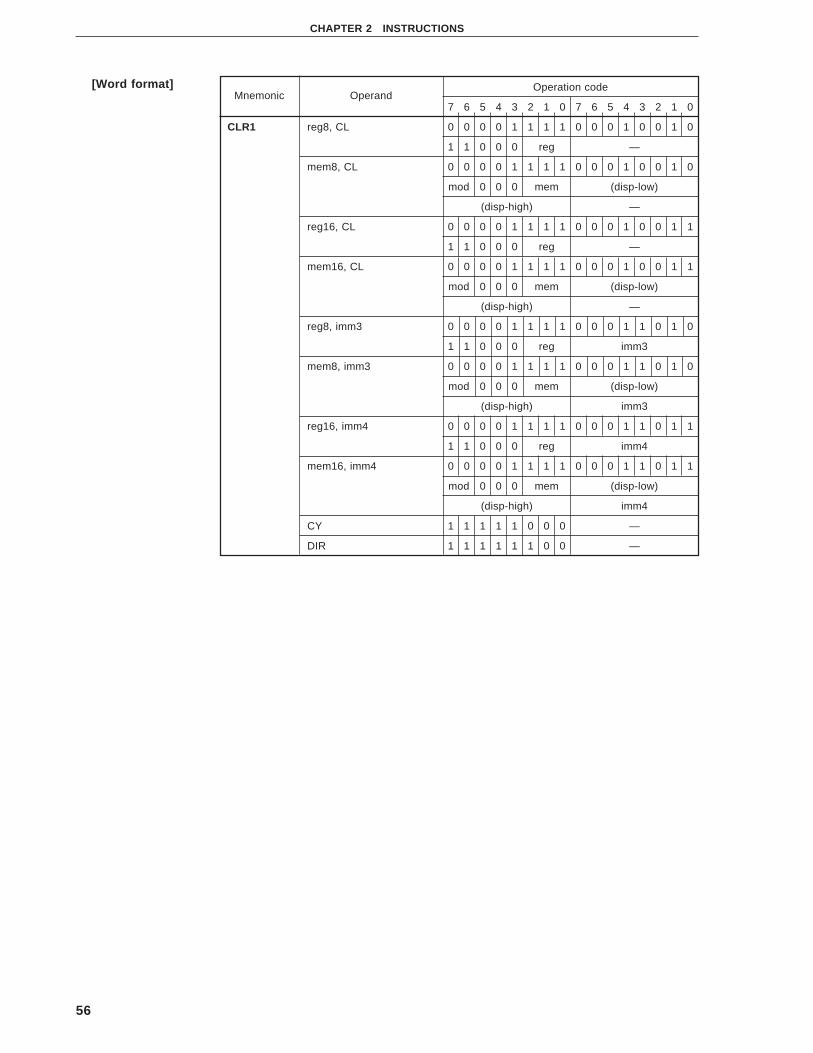
56
CHAPTER 2 INSTRUCTIONS
[Word format]Mnemonic Operand
Operation code
7 6 5 4 3 2 1 0 7 6 5 4 3 2 1 0
CLR1 reg8, CL 0 0 0 0 1 1 1 1 0 0 0 1 0 0 1 0
1 1 0 0 0 reg —
mem8, CL 0 0 0 0 1 1 1 1 0 0 0 1 0 0 1 0
mod 0 0 0 mem (disp-low)
(disp-high) —
reg16, CL 0 0 0 0 1 1 1 1 0 0 0 1 0 0 1 1
1 1 0 0 0 reg —
mem16, CL 0 0 0 0 1 1 1 1 0 0 0 1 0 0 1 1
mod 0 0 0 mem (disp-low)
(disp-high) —
reg8, imm3 0 0 0 0 1 1 1 1 0 0 0 1 1 0 1 0
1 1 0 0 0 reg imm3
mem8, imm3 0 0 0 0 1 1 1 1 0 0 0 1 1 0 1 0
mod 0 0 0 mem (disp-low)
(disp-high) imm3
reg16, imm4 0 0 0 0 1 1 1 1 0 0 0 1 1 0 1 1
1 1 0 0 0 reg imm4
mem16, imm4 0 0 0 0 1 1 1 1 0 0 0 1 1 0 1 1
mod 0 0 0 mem (disp-low)
(disp-high) imm4
CY 1 1 1 1 1 0 0 0 —
DIR 1 1 1 1 1 1 0 0 —

57
CHAPTER 2 INSTRUCTIONS
CompareCMPCompare
[Format] CMP dst, src
[Operand, operation]
[Flag]
[Description] Subtracts the source operand (src) specified by the second operand from the destination
operand (dst) specified by the first operand.
The result of the subtraction is stored nowhere, and only the flags are affected.
[Example] • CMP BL, BYTE PTR [IX]
• CMP CW, [BP+4]
[Number of bytes]
Mnemonic Operand (dst, src) Operation
CMP reg, reg’ dst – src
mem, reg
reg, mem
reg, imm
mem, imm
acc, imm [When W = 0] AL – imm8
[When W = 1] AW – imm16
AC CY V P S Z
× × × × × ×
Mnemonic Operand No. of bytes
CMP reg, reg’ 2
mem, reg 2-4
reg, mem
reg, imm 3, 4
mem, imm 3-6
acc, imm 2, 3
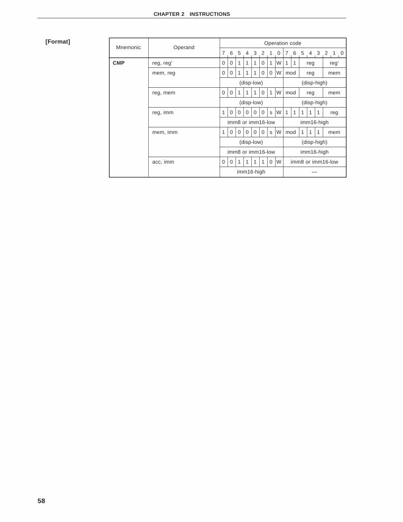
58
CHAPTER 2 INSTRUCTIONS
[Format]Mnemonic Operand
Operation code
7 6 5 4 3 2 1 0 7 6 5 4 3 2 1 0
CMP reg, reg’ 0 0 1 1 1 0 1 W 1 1 reg reg‘
mem, reg 0 0 1 1 1 0 0 W mod reg mem
(disp-low) (disp-high)
reg, mem 0 0 1 1 1 0 1 W mod reg mem
(disp-low) (disp-high)
reg, imm 1 0 0 0 0 0 s W 1 1 1 1 1 reg
imm8 or imm16-low imm16-high
mem, imm 1 0 0 0 0 0 s W mod 1 1 1 mem
(disp-low) (disp-high)
imm8 or imm16-low imm16-high
acc, imm 0 0 1 1 1 1 0 W imm8 or imm16-low
imm16-high —

59
CHAPTER 2 INSTRUCTIONS
Decimal compareCMP4SCompare Nibble String
[Format] CMP4S [DS1-spec:] dst-string, [Seg-spec:] src-string
CMP4S
[Operation] BCD string (IY, CL) ← BCD string (IX, CL)
[Operand]
[Flag]
[Description] Subtracts the packed BCD string addressed by the IX register from the packed BCD string
addressed by the IY register. The result is not stored and only the flags are affected. The
string length (number of BCD digits) is determined by the CL register (the number of digits
is d if the contents of CL is d) in a range of 1 to 254 digits.
The destination string must be always located in a segment specified by the DS1 register,
and the segment cannot be overridden. Although the default segment register of the source
string is the DS0 register, the segment can be overridden, and the string can be located
in a segment specified by any segment register. The format of a packed BCD string is as
follows.
Mnemonic Operand (dst, src)
CMP4S [DS1-spec : ] dst-string, [Seg-spec : ] src-string
None
AC CY V P S Z
U × U U U ×
Caution The BCD string instruction always operates in units of an even number of
digits. If an even number of digits is specified, therefore, the result of the
operation and each flag operation are normal. If an odd number of digits
is specified, however, an operation of an even number of digits, or an odd
number of digits + 1, is executed. As a result, the result of the operation
is an even number of digits and each flag indicates an even number of
digits.
To specify an odd number of digits, therefore, keep this in mind: Execute
the BCD compare instruction, if the number of digits is odd, after clearing
the high-order 4 bits of the most significant byte to “0”.
Memory
Byte offset
Digit offset
+m
+CL 0+1+2+3+4
+0+1
IXIY↓
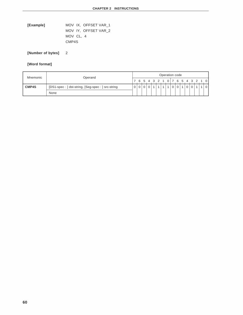
60
CHAPTER 2 INSTRUCTIONS
[Example] MOV IX, OFFSET VAR_1
MOV IY, OFFSET VAR_2
MOV CL, 4
CMP4S
[Number of bytes] 2
[Word format]
Mnemonic OperandOperation code
7 6 5 4 3 2 1 0 7 6 5 4 3 2 1 0
CMP4S [DS1-spec : ] dst-string, [Seg-spec : ] src-string 0 0 0 0 1 1 1 1 0 0 1 0 0 1 1 0
None

61
CHAPTER 2 INSTRUCTIONS
Block compareCMPBKCompare Block
CMPBKB Compare Block Byte
CMPBKW Compare Block Word
[Format] (repeat) CMPBK [Seg-spec:] src-block, [DS1-spec:] dst- block
(repeat) CMPBKB
(repeat) CMPBKW
[Operation] [When W = 0] (IX) – (IY)
DIR = 0: IX ← IX + 1, IY ← IY + 1
DIR = 1: IX ← IX – 1, IY ← IY – 1
[When W = 1] (IX + 1, IX) – (IY + 1, IY)
DIR = 0: IX ← IX + 2, IY ← IY + 2
DIR = 1: IX ← IX – 2, IY ← IY – 2
[Operand]
[Flag]
[Description] Repeatedly subtracts the block addressed by the IY register from the block addressed by
the IX register in byte or word units, and reflects the result on the flags.
The IX and IY registers are automatically incremented (+1/+2) or decremented (–1/–2) for
the next byte/word processing each time data of 1 byte/word has been processed. The
direction of the block is determined by the status of the DIR flag.
Whether data is processed in byte or word units is specified by the attribute of the operand
when the CMPBK instruction is used. When the CMPBKB and CMPBKW instructions are
used, the data is processed in byte and word units, respectively.
The destination block must be always located in a segment specified by the DS1 register,
and the segment cannot be overridden. On the other hand, although the default segment
register of the source block is the DS0 register, the segment can be overridden, and the
block can be located in a segment specified by any segment register.
[Example] CMPBK BYTE_VAR1, BYTE_VAR2
[Number of bytes] 1
Mnemonic Operand
CMPBK [Seg-spec : ] src-block, [DS1-spec : ] dst-block
CMPBKB None
CMPBKW
AC CY V P S Z
× × × × × ×

62
CHAPTER 2 INSTRUCTIONS
[Word format]Mnemonic Operand
Operation code
7 6 5 4 3 2 1 0
CMPBK [Seg-spec : ] src-block, [DS1-spec : ] dst-block 1 0 1 0 0 1 1 W
CMPBKB None
CMPBKW

63
CHAPTER 2 INSTRUCTIONS
Block compare with accumulatorCMPMCompare MultipleCMPMB Compare Multiple Byte
CMPMW Compare Multiple Word
[Format] (repeat) CMPM [DS1-spec:] dst-block
(repeat) CMPMB
(repeat) CMPMW
[Operation] [When W = 0] AL – (IY)
DIR = 0: IY ← IY + 1
DIR = 1: IY ← IY – 1
[When W = 1] AW – (IY + 1, IY)
DIR = 0: IY ← IY + 2
DIR = 1: IY ← IY – 2
[Operand]
[Flag]
[Description] Repeatedly subtracts the block addressed by the IY register from the value of the
accumulator (AL/AW) in byte or word units, and reflects the result on the flags.
The IY register is automatically incremented (+1/+2) or decremented (–1/–2) for the next
byte/word processing each time data of 1 byte/word has been processed. The direction
of the block is determined by the status of the DIR flag.
Whether data is processed in byte or word units is specified by the attribute of the operand
when the CMPM instruction is used. When the CMPMB and CMPMW instructions are used,
the data is processed in byte and word units, respectively.
The destination block must be always located in a segment specified by the DS1 register,
and the segment cannot be overridden.
[Example] • MOV AW, 5555H
MOV BW, 1000H
MOV IY, BW
REPC CMPM WORD PTR [IY]
• REPNC CMPMW
• REPZ CMPMB
[Number of bytes] 1
Mnemonic Operand
CMPM [DS1-spec : ] dst-block
CMPMB None
CMPMW
AC CY V P S Z
× × × × × ×

64
CHAPTER 2 INSTRUCTIONS
[Word format]Mnemonic Operand
Operation code
7 6 5 4 3 2 1 0
CMPM [DS1-spec : ] dst-block 1 0 1 0 1 1 1 W
CMPMB None
CMPMW

65
CHAPTER 2 INSTRUCTIONS
Binary-to-unpacked decimal conversionCVTBDConvert Binary to Decimal
[Format] CVTBD
[Operation] AH ← AL ÷ 0AH
AL ← AL%0AH
[Operand]
[Flag]
[Description] Converts the 8-bit binary number of the AL register into a 2- digit unpacked decimal number.
As a result, the value of the AH register is replaced with the quotient resulting from dividing
the value of the AL register by 10, and then the value of the AL register is replaced with
the remainder resulting from the division.
[Example] MOV AL, 30H
CVTBD
[Number of bytes] 2
[Word format]
AC CY V P S Z
U U U × × ×
Mnemonic Operand
CVTBD None
Mnemonic OperandOperation code
7 6 5 4 3 2 1 0 7 6 5 4 3 2 1 0
CVTBD None 1 1 0 1 0 1 0 0 0 0 0 0 1 0 1 0
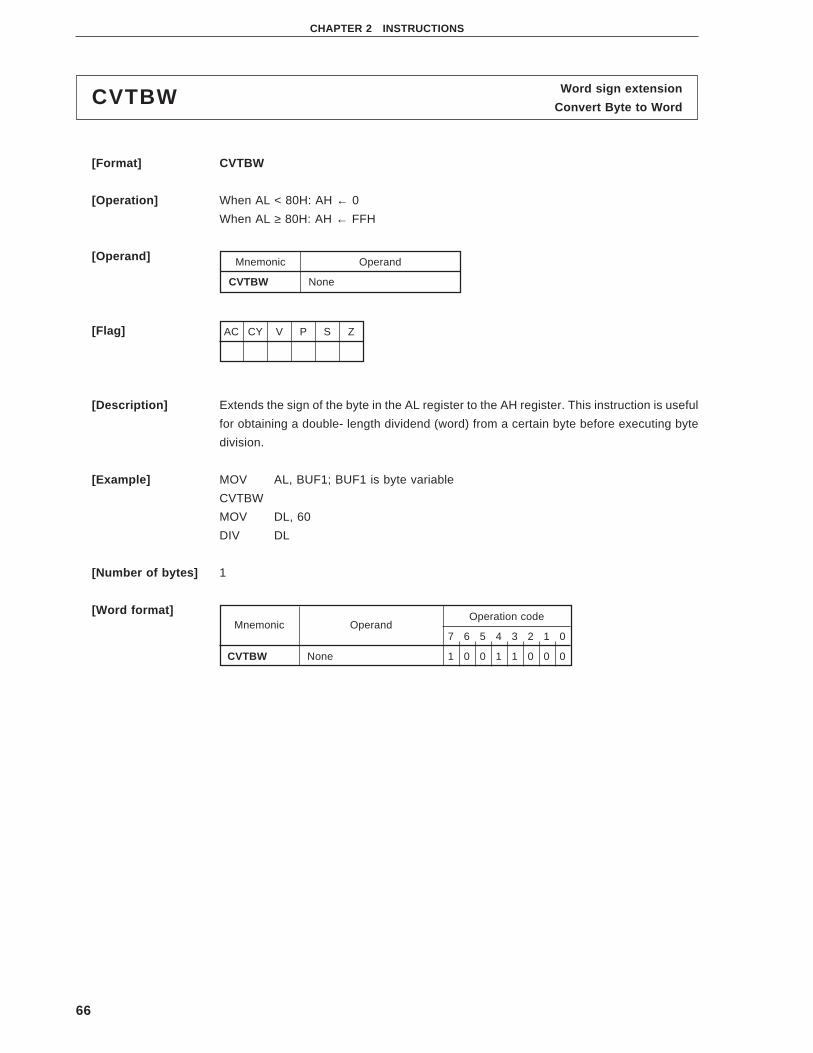
66
CHAPTER 2 INSTRUCTIONS
Word sign extensionCVTBWConvert Byte to Word
[Format] CVTBW
[Operation] When AL < 80H: AH ← 0
When AL ≥ 80H: AH ← FFH
[Operand]
[Flag]
[Description] Extends the sign of the byte in the AL register to the AH register. This instruction is useful
for obtaining a double- length dividend (word) from a certain byte before executing byte
division.
[Example] MOV AL, BUF1; BUF1 is byte variable
CVTBW
MOV DL, 60
DIV DL
[Number of bytes] 1
[Word format]
AC CY V P S Z
Mnemonic Operand
CVTBW None
Mnemonic OperandOperation code
7 6 5 4 3 2 1 0
CVTBW None 1 0 0 1 1 0 0 0

67
CHAPTER 2 INSTRUCTIONS
Unpacked decimal-to-binary conversionCVTDBConvert Decimal to Binary
[Format] CVTDB
[Operation] AL ← AH × 0AH + AL
AH ← 0
[Operand]
[Flag]
[Description] Converts the 2-digit unpacked decimal number of the AH and AL registers into a 16-bit
binary number.
As a result, the value of the AL register is replaced with the sum of value of the AL register
and the result of multiplying the value of the AH register by 10, and the value of the AH
register is replaced with 0.
[Example] MOV AW, [BW]
CVTDB
[Number of bytes] 2
[Word format]
AC CY V P S Z
U U U × × ×
Mnemonic Operand
CVTDB None
Mnemonic OperandOperation code
7 6 5 4 3 2 1 0 7 6 5 4 3 2 1 0
CVTDB None 1 1 0 1 0 1 0 1 0 0 0 0 1 0 1 0

68
CHAPTER 2 INSTRUCTIONS
Double word sign extensionCVTWLConvert Word to Long Word
[Format] CVTWL
[Operation] When AW < 8000H: DW ← 0
When AW ≥ 8000H: DW ← FFFFH
[Operand]
[Flag]
[Description] Extends the sign of the word of the AW register to the DW register. This instruction is useful
for obtaining a double-length (double word) dividend from a certain word before executing
word division.
[Example] MOV AW, BUFFER
CVTWL
DIV CW
[Number of bytes] 1
[Word format]
AC CY V P S Z
Mnemonic Operand
CVTWL None
Mnemonic OperandOperation code
7 6 5 4 3 2 1 0
CVTWL None 1 0 0 1 1 0 0 1

69
CHAPTER 2 INSTRUCTIONS
Conditional loop where CW ≠ 0DBNZDecrement and Branch if Not Zero
[Format] DBNZ short-label
[Operation] CW ← CW – 1
Where CW ≠ 0: PC ← PC + ext-disp8
[Operand]
[Flag]
[Description] Decrements the value of the CW register (–1) and, if the value of the CW register is not
zero as a result, loads the current PC value with an 8-bit displacement added (actually,
sign-extended 16 bits) to the PC.
Execution can branch in the segment where this instruction is placed and in an address
range of –128 to +127 bytes. Execution goes on to the next instruction if the above condition
is not satisfied.
[Example] LP21:
SHL AL, 1
DBNZ LP21 ; LP21 = label
[Number of bytes] 2
[Word format]
AC CY V P S Z
Mnemonic Operand
DBNZ short-label
...
Mnemonic OperandOperation code
7 6 5 4 3 2 1 0 7 6 5 4 3 2 1 0
DBNZ short-label 1 1 1 0 0 0 1 0 disp8

70
CHAPTER 2 INSTRUCTIONS
Conditional loop where CW ≠ 0 and Z = 1DBNZEDecrement and Branch if Not Zero and Equal
[Format] DBNZE short-label
[Operation] CW ← CW – 1
Where CW ≠ 0 and Z = 1: PC ← PC + ext-disp8
[Operand]
[Flag]
[Description] Decrements the value of the CW register (–1) and, if the value of the CW register is not
zero and the Z flag is set to 1 as a result, loads the current PC value with an 8-bit
displacement added (actually, sign-extended 16 bits) to the PC.
Execution can branch in the segment where this instruction is placed and in an address
range of –128 to +127 bytes.
Execution goes on to the next instruction if the above condition is not satisfied.
[Example] LP20:
AND AL, BL
DBNZE LP20 ; LP20 = label
[Number of bytes] 2
[Word format]
AC CY V P S Z
Mnemonic Operand
DBNZE short-label
...
Mnemonic OperandOperation code
7 6 5 4 3 2 1 0 7 6 5 4 3 2 1 0
DBNZE short-label 1 1 1 0 0 0 0 1 disp8

71
CHAPTER 2 INSTRUCTIONS
Conditional loop where CW ≠ 0 and Z = 0DBNZNEDecrement and Branch if Not Zero and Not Equal
[Format] DBNZNE short-label
[Operation] CW ← CW – 1
Where CW ≠ 0: PC ← PC + ext-disp8
[Operand]
[Flag]
[Description] Decrements the value of the CW register (–1) and, if the value of the CW register is not
zero and the Z flag is cleared as a result, loads the current PC value with an 8-bit
displacement added (actually, sign-extended 16 bits) to the PC.
Execution can branch in the segment where this instruction is placed and in an address
range of –128 to +127 bytes.
Execution goes on to the next instruction if the above condition is not satisfied.
[Example] LP19:
AND AL, 0FFH
DBNZNE SHORT LP19 ; LP19 = label
[Number of bytes] 2
[Word format]
AC CY V P S Z
Mnemonic Operand
DBNZNE short-label
Mnemonic OperandOperation code
7 6 5 4 3 2 1 0 7 6 5 4 3 2 1 0
DBNZNE short-label 1 1 1 0 0 0 0 0 disp8
...
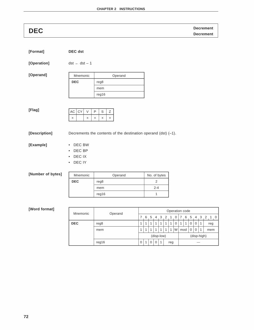
72
CHAPTER 2 INSTRUCTIONS
DecrementDEC Decrement
[Format] DEC dst
[Operation] dst ← dst – 1
[Operand]
[Flag]
[Description] Decrements the contents of the destination operand (dst) (–1).
[Example] • DEC BW
• DEC BP
• DEC IX
• DEC IY
[Number of bytes]
[Word format]
Mnemonic Operand
DEC reg8
mem
reg16
AC CY V P S Z
× × × × ×
Mnemonic Operand No. of bytes
DEC reg8 2
mem 2-4
reg16 1
Mnemonic OperandOperation code
7 6 5 4 3 2 1 0 7 6 5 4 3 2 1 0
DEC reg8 1 1 1 1 1 1 1 0 1 1 0 0 1 reg
mem 1 1 1 1 1 1 1 W mod 0 0 1 mem
(disp-low) (disp-high)
reg16 0 1 0 0 1 reg —

73
CHAPTER 2 INSTRUCTIONS
Disable maskable interruptDIDisable Interrupt
[Format] DI
[Operation] IE ← 0
[Operand]
[Flag]
[Description] Resets the IE flag to 0 and disables the maskable interrupt. This instruction does not disable
the non-maskable interrupt request and software interrupt request.
[Example] DI
PUSH R
[Number of bytes] 1
[Word format]
AC CY V P S Z IE
0
Mnemonic Operand
DI None
Mnemonic OperandOperation code
7 6 5 4 3 2 1 0
DI None 1 1 1 1 1 0 1 0

74
CHAPTER 2 INSTRUCTIONS
Deletes a stack frameDISPOSEDispose a Stack Frame
[Format] DISPOSE
[Operation] SP ← BP
BP ← (SP + 1, SP)
SP ← SP + 2
[Operand]
[Flag]
[Description] This instruction releases one frame of the stack frame created by the PREPARE instruction.
A pointer value indicating one frame before is loaded to the BP, and a pointer value
indicating the lowest frame is loaded to the SP.
[Example] DISPOSE
[Number of bytes] 1
[Word format]
Mnemonic OperandOperation code
7 6 5 4 3 2 1 0
DISPOSE None 1 1 0 0 1 0 0 1
AC CY V P S Z
Mnemonic Operand
DISPOSE None

75
CHAPTER 2 INSTRUCTIONS
Signed divisionDIVDivide Signed
[Format] DIV dst
[Operand, operation]
[Flag]
Mnemonic Operand (dst) Operation
DIV reg8 temp ← AW
Where temp ÷ dst > 0 and temp ÷ dst ≤ 7FH or,
where temp ÷ dst < 0 and temp ÷ dst > 0 – 7FH – 1,
AH ← temp%dst
AL ← temp ÷ dst
Where temp ÷ dst > 0 and temp ÷ dst > 7FH or,
where temp ÷ dst < 0 and temp ÷ dst ≤ 0 – 7FH – 1,
quotient and remainder are undefined.
mem8 TA ← (001H, 000H)
TC ← (003H, 002H)
SP ← SP – 2, (SP + 1, SP) ← PSW
IE ← 0, BRK ← 0
SP ← SP – 2, (SP + 1, SP) ← PS
PS ← TC
SP ← SP – 2, (SP + 1, SP) ← PC
PC ← TA
reg16 temp ← DW, AW
Where temp ÷ dst > 0 and temp ÷ dst ≤ 7FFFH or,
where temp ÷ dst < 0 and temp ÷ dst > 0 – 7FFFH – 1,
DW ← temp%dst
AW ← temp ÷ dst
Where temp ÷ dst > 0 and temp ÷ dst > 7FFFH or,
where temp ÷ dst < 0 and temp ÷ dst ≤ 0 – 7FFFH – 1,
quotient and remainder are undefined.
mem16 TA ← (001H, 000H)
TC ← (003H, 002H)
SP ← SP – 2, (SP + 1, SP) ← PSW
IE ← 0, BRK ← 0
SP ← SP – 2, (SP + 1, SP) ← PS
PS ← TC
SP ← SP – 2, (SP + 1, SP) ← PC
PC ← TA
AC CY V P S Z
U U U U U U

76
CHAPTER 2 INSTRUCTIONS
[Description] • Where src = reg8 or src = mem8
Divides the value of the AW register by the contents of the destination operand (dst)
with sign.
The quotient is stored to the AL register, and the remainder is stored to the AH register.
The maximum value of the positive quotient is +127 (7FH), and the minimum value is
–127 (81H). If the quotient is positive and is greater than the maximum value, or if the
quotient is negative and is less than the minimum value, vector 0 interrupt occurs
(especially where src = 00H), and the quotient and remainder are undefined. If the
quotient is not an integer, it is rounded to an integer, and the remainder has the same
sign as the dividend.
• Where src = reg16 or src = mem16
Divides the values of the AW and DW registers by the contents of the destination
operand (dst) with sign.
The quotient is stored to the AW register, and the remainder is stored to the DW register.
The maximum value of the positive quotient is +32767 (7FFFH), and the minimum value
is –32767 (8001H). If the quotient is positive and is greater than the maximum value,
or if the quotient is negative and is less than the minimum value, vector 0 interrupt occurs
(especially where src = 0000H), and the quotient and remainder are undefined. If the
quotient is not an integer, it is rounded to an integer, and the remainder has the same
sign as the dividend.
[Example] To divide 32-bit data DW:AW by contents of memory 0:50
MOV BW, 0
MOV DS0, BW
MOV IX, 50H
DIV DS0:WORD PTR [IX]
[Number of bytes]
[Word format]
Mnemonic Operand No. of bytes
DIV reg8 2
mem8 2-4
reg16 2
mem16 2-4
Mnemonic OperandOperation code
7 6 5 4 3 2 1 0 7 6 5 4 3 2 1 0
DIV reg8 1 1 1 1 0 1 1 0 1 1 1 1 1 reg
mem8 1 1 1 1 0 1 1 0 mod 1 1 1 mem
(disp-low) (disp-high)
reg16 1 1 1 1 0 1 1 1 1 1 1 1 1 reg
mem16 1 1 1 1 0 1 1 1 mod 1 1 1 mem
(disp-low) (disp-high)

77
CHAPTER 2 INSTRUCTIONS
Unsigned divisionDIVUDivide Unsigned
[Format] DIVU dst
[Operand, operation]
[Flag]
Mnemonic Operand (dst) Operation
DIVU reg8 temp ← AW
Where temp ÷ dst ≥ FFH:
AH ← temp%dst
AL ← temp ÷ dst
Where temp ÷ dst > FFH:
TA ← (001H, 000H)
mem8 TC ← (003H, 002H)
SP ← SP – 2, (SP + 1, SP) ← PSW
IE ← 0, BRK ← 0
SP ← SP – 2, (SP + 1, SP) ← PS
RS ← TC
SP ← SP – 2, (SP + 1, SP) ← PC
PC ← TA
reg16 temp ← DW, AW
Where temp ÷ dst ≥ FFFFH:
DW ← temp%dst
AW ← temp ÷ dst
Where temp ÷ dst > FFFFH:
TA ← (001H, 000H)
mem16 TC ← (003H, 002H)
SP ← SP – 2, (SP + 1, SP) ← PSW
IE ← 0, BRK ← 0
SP ← SP – 2, (SP + 1, SP) ← PS
RS ← TC
SP ← SP – 2, (SP + 1, SP) ← PC
PC ← TA
AC CY V P S Z
U U U U U U

78
CHAPTER 2 INSTRUCTIONS
[Description] • Where src = reg8 or src = mem8
Divides the value of the AW register by the contents of the destination operand (dst)
without sign. The quotient is stored to the AL register, and the remainder is stored to
the AH register.
If the quotient exceeds the capacity of the AL register (FFH), vector 0 interrupt occurs
(especially where src = 00H), and the quotient and remainder are undefined. If the
quotient is not an integer, it is rounded to an integer.
• Where src = reg16 or src = mem16
Divides the values of the AW and DW registers by the contents of the destination
operand (dst) without sign. The quotient is stored to the AW register, and the remainder
is stored to the DW register.
If the quotient exceeds the capacity of the AW register (FFFFH), vector 0 interrupt occurs
(especially where src = 0000H), and the quotient and remainder are undefined. If the
quotient is not an integer, it is rounded to an integer.
[Example] To divide 5 by 3
MOV AW, 5
MOV DL, 3
DIVU DL
; AH = 2 AL = 1
[Number of bytes]
[Word format]
Mnemonic Operand No. of bytes
DIVU reg8 2
mem8 2-4
reg16 2
mem16 2-4
Mnemonic OperandOperation code
7 6 5 4 3 2 1 0 7 6 5 4 3 2 1 0
DIVU reg8 1 1 1 1 0 1 1 0 1 1 1 1 0 reg
mem8 1 1 1 1 0 1 1 0 mod 1 1 0 mem
(disp-low) (disp-high)
reg16 1 1 1 1 0 1 1 1 1 1 1 1 0 reg
mem16 1 1 1 1 0 1 1 1 mod 1 1 0 mem
(disp-low) (disp-high)

79
CHAPTER 2 INSTRUCTIONS
Segment override prefixDS0:Data Segment 0DS1:Data Segment 1
PS: Program Segment
SS: Stack Segment
[Format] DS0:
DS1:
PS:
SS:
[Operation] Segment override prefix
[Operand]
[Flag]
[Description] When a memory operand is accessed for which segment override is enabled, specifies a
segment register that is described as an operand and used. Even if this instruction is not
directly described, segment override can be specified by the assembler if the ASSUME
(assembler directive) is used.
Caution The hardware interrupt (maskable interrupt and non-maskable interrupt)
request and single-step break cannot be accepted between this instruction
and the next instruction.
[Example] MOV DW, DS1: [BW]; Default segment register is DS0
[Number of bytes] 1
[Word Format]
Mnemonic Operand
DS0: None
DS1:
PS:
SS:
AC CY V P S Z
Mnemonic OperandOperation code
7 6 5 4 3 2 1 0
DS0: None 0 0 1 sreg 1 1 0
DS1:
PS:
SS:

80
CHAPTER 2 INSTRUCTIONS
Enables maskable interruptEIEnable Interrupt
[Format] EI
[Operation] IE ← 1
[Operand]
[Flag]
[Description] Sets the IE flag to 1 and enables the maskable interrupt. However, the interrupt is actually
enabled when the single instruction following the EI instruction is executed.
[Example] POP R
EI
[Number of bytes] 1
[Word format]
AC CY V P S Z IE
1
Mnemonic Operand
EI None
Mnemonic OperandOperation code
7 6 5 4 3 2 1 0
EI None 1 1 1 1 1 0 1 1

81
CHAPTER 2 INSTRUCTIONS
Extracts bit fieldEXTExtract Bit Field
[Format] EXT dst, src
[Operation] AW ← 16-bit field
[Operand]
[Flag]
[Description] Loads bit field data of the bit length specified by the source operand (src) from a memory
area determined by byte offset addressed by the IX register and the bit offset specified by
the 8-bit register described as the first operand to the AW register. At this time, 0 is loaded
to the high-order bits of the AW register.
After completion of the transfer, the IX register and the 8-bit register specified by the first
operand are automatically updated to indicate the next bit field, as follows:
reg8 ← reg8 + src + 1
if reg8 > 15 then
{
reg8 ← reg8 – 16
IX ← IX + 2
}
Mnemonic Operand (dst, src)
EXT reg8, reg8’
reg8, imm4
AC CY V P S Z
U U U U U U
����↓
↓ ↓
����
15 0
0AW
Bit length Bit offset(IX)
Byte offset
Byte boundary Segment base(default DS0)
Memory

82
CHAPTER 2 INSTRUCTIONS
The value of the 8-bit register of the first operand that specifies a bit offset (15 bits max.)
must be 0 to 15. The value of the source operand (src) that specifies the bit length (16 bits
max.) must be 0 to 15. 0 indicates a length of 1 bit and 15 indicates a length of 16 bits.
The bit field data can straddle a byte boundary of memory.
The default segment register for the bit field of the source is the DS0 register, and segments
can be overridden. The data can be located in any segment that is specified by any segment
register.
Caution Clear the high-order 4 bits of reg8 or reg8’ to 0.
[Example] • EXT CL, DL
• EXT CL, 8
[Number of bytes]
[Word format]
Mnemonic Operand No. of bytes
EXT reg8, reg8’ 3
reg8, imm4 4
Mnemonic OperandOperation code
7 6 5 4 3 2 1 0 7 6 5 4 3 2 1 0
EXT reg8, reg8’ 0 0 0 0 1 1 1 1 0 0 1 1 0 0 1 1
1 1 reg’ reg –
reg8, imm4 0 0 0 0 1 1 1 1 0 0 1 1 1 0 1 1
1 1 0 0 0 reg imm4

83
CHAPTER 2 INSTRUCTIONS
Controls floating-point coprocessorFPO1Floating Point Operation 1
[Format] (1) FPO1 fp-op
(2) FPO1 fp-op, mem
[Operand, operation]
Format (1)
Format (2)
[Flag]
[Description] Format (1): This instruction is used to control an externally connected floating-point
coprocessor. When the CPU fetches this instruction, it executes nothing but
lets the coprocessor perform processing.
Format (2): This instruction is used to control an externally connected floating-point
coprocessor. When the CPU fetches this instruction, it lets the coprocessor
perform processing and, if necessary, executes only auxiliary processing
(such as effective address calculation, physical address generation, and
starting a memory read cycle). The CPU does not read the data on the data
bus in the memory read cycle started by CPU.
[Example] • FPO1 010101010B
• FPO1 0FFH
• FPO1 6, BYTE PTR [IX]
• FPO1 4, WORD_VAR
[Number of bytes]
Mnemonic Operand Operation
FPO1 fp-op No operation
Mnemonic Operand Operation
FPO1 fp-op, mem Data bus ← (mem)
AC CY V P S Z
Mnemonic Operand No. of bytes
FPO1 fp-op 2
fp-op, mem 2-4

84
CHAPTER 2 INSTRUCTIONS
[Word format]Mnemonic Operand
Operation code
7 6 5 4 3 2 1 0 7 6 5 4 3 2 1 0
FPO1 fp-op 1 1 0 1 1 X X X 1 1 Y Y Y Z Z Z
fp-op, mem 1 1 0 1 1 X X X mod Y Y Y mem
(disp-low) (disp-high)
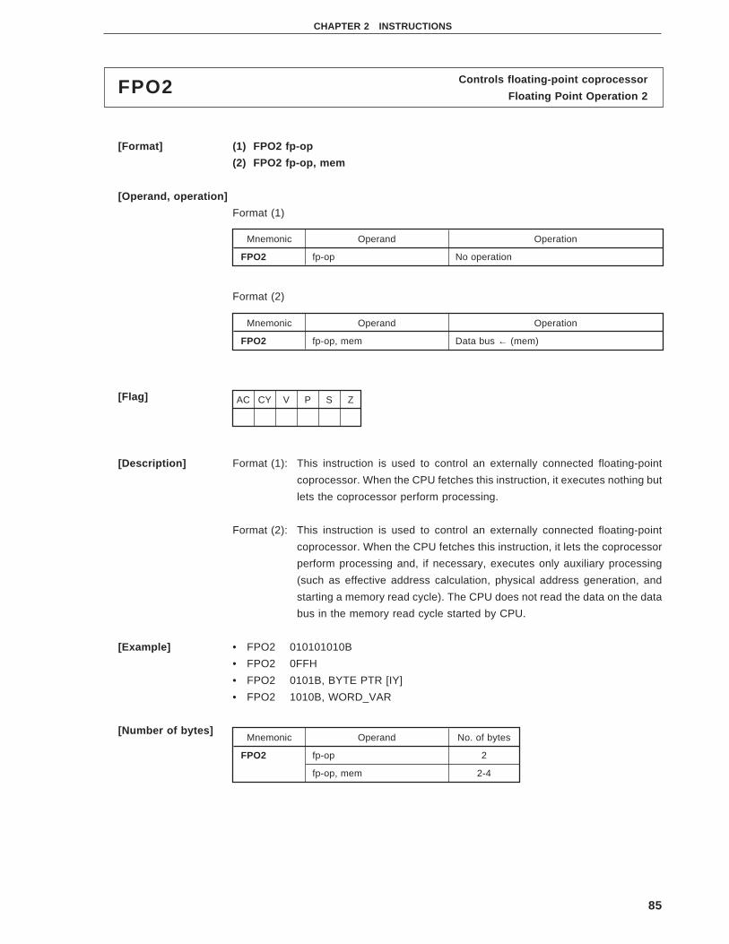
85
CHAPTER 2 INSTRUCTIONS
Controls floating-point coprocessorFPO2Floating Point Operation 2
[Format] (1) FPO2 fp-op
(2) FPO2 fp-op, mem
[Operand, operation]
Format (1)
Format (2)
[Flag]
[Description] Format (1): This instruction is used to control an externally connected floating-point
coprocessor. When the CPU fetches this instruction, it executes nothing but
lets the coprocessor perform processing.
Format (2): This instruction is used to control an externally connected floating-point
coprocessor. When the CPU fetches this instruction, it lets the coprocessor
perform processing and, if necessary, executes only auxiliary processing
(such as effective address calculation, physical address generation, and
starting a memory read cycle). The CPU does not read the data on the data
bus in the memory read cycle started by CPU.
[Example] • FPO2 010101010B
• FPO2 0FFH
• FPO2 0101B, BYTE PTR [IY]
• FPO2 1010B, WORD_VAR
[Number of bytes]
Mnemonic Operand Operation
FPO2 fp-op No operation
AC CY V P S Z
Mnemonic Operand Operation
FPO2 fp-op, mem Data bus ← (mem)
Mnemonic Operand No. of bytes
FPO2 fp-op 2
fp-op, mem 2-4

86
CHAPTER 2 INSTRUCTIONS
[Word format]Mnemonic Operand
Operation code
7 6 5 4 3 2 1 0 7 6 5 4 3 2 1 0
FPO2 fp-op 0 1 1 0 0 1 1 X 1 1 Y Y Y Z Z Z
fp-op, mem 0 1 1 0 0 1 1 X mod Y Y Y mem
(disp-low) (disp-high)

87
CHAPTER 2 INSTRUCTIONS
AC CY V P S Z
Mnemonic Operand
HALT None
Mnemonic OperandOperation code
7 6 5 4 3 2 1 0
HALT None 1 1 1 1 0 1 0 0
HaltHALTHalt
[Format] HALT
[Operation] CPU Halt
[Operand]
[Flag]
[Description] Stops clock supply to the CPU and sets the standby mode. The standby mode is released
by the following:
• Reset input
• Maskable interrupt request input
• Non-maskable interrupt request input
[Example] HALT
[Number of bytes] 1
[Word format]
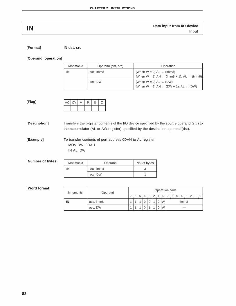
88
CHAPTER 2 INSTRUCTIONS
Mnemonic Operand (dst, src) Operation
IN acc, imm8 [When W = 0] AL ← (imm8)
[When W = 1] AH ← (imm8 + 1), AL ← (imm8)
acc, DW [When W = 0] AL ← (DW)
[When W = 1] AH ← (DW + 1), AL ← (DW)
AC CY V P S Z
Mnemonic Operand No. of bytes
IN acc, imm8 2
acc, DW 1
Data input from I/O deviceINInput
[Format] IN dst, src
[Operand, operation]
[Flag]
[Description] Transfers the register contents of the I/O device specified by the source operand (src) to
the accumulator (AL or AW register) specified by the destination operand (dst).
[Example] To transfer contents of port address 0DAH to AL register
MOV DW, 0DAH
IN AL, DW
[Number of bytes]
[Word format]Mnemonic Operand
Operation code
7 6 5 4 3 2 1 0 7 6 5 4 3 2 1 0
IN acc, imm8 1 1 1 0 0 1 0 W imm8
acc, DW 1 1 1 0 1 1 0 W —

89
CHAPTER 2 INSTRUCTIONS
IncrementINCIncrement
[Format] INC dst
[Operation] dst ← dst + 1
[Operand]
[Flag]
[Description] Increments the contents of the destination operand (dst) (+1).
[Example] • INC DW
• INC BP
• INC SP
[Number of bytes]
[Word format]
Mnemonic Operand (dst)
INC reg8
mem
reg16
AC CY V P S Z
× × × × ×
Mnemonic Operand No. of bytes
INC reg8 2
mem 2-4
reg16 1
Mnemonic OperandOperation code
7 6 5 4 3 2 1 0 7 6 5 4 3 2 1 0
INC reg8 1 1 1 1 1 1 1 0 1 1 0 0 0 reg
mem 1 1 1 1 1 1 1 W mod 0 0 0 mem
(disp-low) (disp-high)
reg16 0 1 0 0 0 reg —

90
CHAPTER 2 INSTRUCTIONS
Block transfer between I/O and memoryINMInput Multiple
[Format] (repeat) INM [DS1-spec:] dst-block, DW
[Operation] [When W = 0] (IY) ← (DW)
DIR = 0: IY ← IY + 1
DIR = 1: IY ← IY – 1
[When W = 1] (IY + 1, IY) ← (DW + 1, DW)
DIR = 0: IY ← IY + 2
DIR = 1: IY ← IY – 2
[Operand]
[Flag]
[Description] Transfers the register contents of the I/O device addressed by the DW register to the
memory addressed by the IY register. The number of times the data is repeatedly
transferred is controlled by the REP instruction, a repeat prefix used in pairs with this
instruction. When the data is repeatedly transferred, the contents of the DW register
(address of the I/O device) are fixed, but the value of the IY register is automatically
incremented (+1/+2) or decremented (–1/–2) to transfer the next byte/word each time 1-
byte/word data has been transferred. The direction of the block is determined by the status
of the DIR flag.
Whether data is transferred in byte or word units is determined by the attribute of the
operand.
The INM instruction is used with a repeat prefix, REP instruction.
The destination block must be always located in a segment specified by the DS1 register
and segments cannot be overridden.
[Example] • To load contents of port address 0DAH (byte data) to memory work area
MOV AW, 0
MOV DS1, AW
MOV IY, 50H
MOV DW, 0DAH
INM DS1:BYTE PTR [IY], DW
• To load contents of port address 0DAH (byte data) to memory 0:0 through 0:FFH
MOV AW, 0
MOV DS1, AW
MOV IY, 0
MOV DW, 0DAH
MOV CW, 0FFH
REP INM DS1: BYTE PTR [IY], DW
Mnemonic Operand
INM [DS1-spec : ] dst-block, DW
AC CY V P S Z

91
CHAPTER 2 INSTRUCTIONS
[Number of bytes] 1
[Word format]Mnemonic Operand
Operation code
7 6 5 4 3 2 1 0
INM [DS1-spec : ] dst-block, DW 0 1 1 0 1 1 0 W

92
CHAPTER 2 INSTRUCTIONS
Inserts bit fieldINSInsert Bit Field
[Format] INS dst, src
[Operation] 16-bit field ← AW
[Operand]
[Flag]
[Description] Of the 16-bit data of the AW register, transfers the low-order bit data of the length specified
by the source operand (src) to a memory area that is determined by the byte offset
addressed by the DS1 and IY registers and the bit offset specified by the 8- bit register
described as the first operand.
After the data has been transferred, the IY register and the 8- bit register specified by the
first operand are automatically updated as follows to indicate the next bit field.
reg ← reg8 + src + 1
if reg8 > 15 then
{
reg8 ← reg8 – 16
IY ← IY + 2
}
Mnemonic Operand (dst, src)
INS reg8, reg8’
reg8, imm4
AC CY V P S Z
U U U U U U
���� ↓↓
����
15 0
0AW
Bit offset(IY)
Byte offset
Byte boundarySegment base
(DS1)
Memory
src dst
↓
Bit length

93
CHAPTER 2 INSTRUCTIONS
The value of the 8-bit register of the first operand that specifies the bit offset (15 bits max.)
must be 0 to 15. The value of the source operand (src) that specifies the bit length (16 bits
max.) must be 0 to 15. 0 indicates a length of 1 bit and 15 indicates a length of 16 bits.
The bit field data can straddle a byte boundary of memory. The bit field of the destination
must be always located in a segment specified by the DS1 register, and segments can be
overridden.
Caution Clear the high-order 4 bits of reg8 or reg8’ to 0.
[Example] • INS DL, CL
• INS DL, 12
[Number of bytes]
[Word format]
Mnemonic Operand No. of bytes
INS reg8, reg8’ 3
reg8, imm4 4
Mnemonic OperandOperation code
7 6 5 4 3 2 1 0 7 6 5 4 3 2 1 0
INS reg8, reg8’ 0 0 0 0 1 1 1 1 0 0 1 1 0 0 0 1
1 1 reg’ reg —
reg8, imm4 0 0 0 0 1 1 1 1 0 0 1 1 1 0 0 1
1 1 0 0 0 reg imm4
94
CHAPTER 2 INSTRUCTIONS
Loads effective addressLDEALoad Effective Address
[Format] LDEA reg16, mem16
[Operation] reg16 ← mem16
[Operand]
[Flag]
[Description] Loads an effective address (offset) generated by the second operand to a 16-bit general-
purpose register specified by the first operand.
This instruction is used to set the first value of an operand address to a register that is
automatically used by the TRANS instruction or primitive block transfer instruction to
specify an operand.
[Example] To load offset of effective address of procedure INT_PROC to AW register
LDEA AW, INT_PROC
LDEA AW, [BP] VAR01 + 2
[Number of bytes] 2 to 4
[Word format]
Mnemonic Operand (dst, src)
LDEA reg16, mem16
AC CY V P S Z
Mnemonic OperandOperation code
7 6 5 4 3 2 1 0 7 6 5 4 3 2 1 0
LDEA reg16, mem16 1 0 0 0 1 1 0 1 mod reg mem
(disp-low) (disp-high)

95
CHAPTER 2 INSTRUCTIONS
Block loadLDMLoad MultipleLDMB Load Multiple Byte
LDMW Load Multiple Word
[Format] (repeat) LDM [Seg-spec:] src-block
(repeat) LDMB
(repeat) LDMW
[Operation] [When W = 0] AL ← (IX)
DIR = 0: IX ← IX + 1
DIR = 1: IX ← IX – 1
[When W = 1] AW ← (IX + 1, IX)
DIR = 0: IX ← IX + 2
DIR = 1: IX ← IX – 2
[Operand]
[Flag]
[Description] Repeatedly transfers the block addressed by the IX register to the accumulator (AL/AW)
in byte or word units.
The IX register is automatically incremented (+1/+2) or decremented (–1/–2) for the next
byte/word processing each time data of 1 byte/word has been processed. The direction
of the block is determined by the status of the DIR flag.
Whether data is processed in byte or word units is specified by the attribute of the operand
when the LDM instruction is used. When the LDMB and LDMW instructions are used, the
data is processed in byte and word units, respectively.
The default segment register of the source block is the DS0 register and segments can
be overridden. The source block can be located in a segment specified by any segment
register.
[Example] • REP LDM DS1: BYTE_VAR ; DS1 segment
• REP LDMB ; DS0 segment
[Number of bytes] 1
Mnemonic Operand
LDM [Seg-spec : ] src-block
LDMB None
LDMW
AC CY V P S Z

96
CHAPTER 2 INSTRUCTIONS
[Word format]Mnemonic Operand
Operation code
7 6 5 4 3 2 1 0
LDM [Seg-spec : ]src-block 1 0 1 0 1 1 0 W
LDMB None
LDMW

97
CHAPTER 2 INSTRUCTIONS
Transfers dataMOVMove
[Format] (1) MOV dst, src
(2) MOV dst1, dst2, src
[Operand, operation]
Format (1)
Format (2)
[Flag] Where operand is PSW or AH Other than left
Mnemonic Operand (dst, src) Operation
MOV reg, reg’ dst ← src
mem, reg
reg, mem
mem, imm
reg, imm
acc, dmem [When W = 0] AL ← (dmem)
[When W = 1] AH ← (dmem + 1), AL ← (dmem)
dmem, acc [When W = 0] (dmem) ← AL
[When W = 1] (dmem + 1) ← AH, (dmem) ← AL
sreg, reg16 dst ← src
sreg, mem16
reg16, sreg
mem16, sreg
AH, PSW AH ← S, Z, ×, AC, ×, P, ×, CY
PSW, AH S, Z, ×, AC, ×, P, ×, CY ← AH
Mnemonic Operand (dst1, dst2, src) Operation
DS0, reg16, mem32 reg16 ← (mem32)
DS0 ← (mem32 + 2)
DS1, reg16, mem32 reg16 ← (mem32)
DS1 ← (mem32 + 2)
AC CY V P S Z
× × × × ×
AC CY V P S Z

98
CHAPTER 2 INSTRUCTIONS
[Description] Format (1): Transfers the contents of the source operand (src) specified by the second
operand to the destination operand (dst) specified by the first operand.
If the operands are AH, PSW, the S, Z, AC, P, and CY flags are transferred
to the AH register. Bits 1, 3, and 5 of the AH register are undefined as a result.
If the operands are PSW, AH, bits 2, 4, 6, and 7 of the AH register are
transferred to the S, Z, AC, P, and CY flags of the PSW, respectively.
Caution If dst = sreg or src = sreg, the hardware interrupt (maskable
interrupt or non-maskable interrupt) request and single-step
break cannot be accepted between this instruction and the
next instruction.
Format (2): Transfers the low-order 16 bits (offset word of 32-bit pointer variable) of the
32-bit memory addressed by the source operand (src) to a 16-bit register
specified by destination operand 2 (dst2), and the high-order 16 bits (segment
word) of the 32-bit memory to a segment register (DS0 or DS1 register)
specified by destination operand 1 (dst1).
[Example] To write 55H to memory 0:50H
MOV AW, 0
MOV DS1, AW
MOV IY, 50H
MOV DL, 55H
MOV DS1: [IY], DL
[Number of Bytes] Mnemonic Operand No. of bytes
MOV reg, reg’ 2
mem, reg 2-4
reg, mem
mem, imm 3-6
reg, imm 2, 3
acc, dmem 3
dmem, acc
sreg, reg16 2
sreg, mem16 2-4
reg16, sreg 2
mem16, sreg 2-4
DS0, reg16, mem32
DS1, reg16, mem32
AH, PSW 1
PSW, AH

99
CHAPTER 2 INSTRUCTIONS
[Word format]Mnemonic Operand
Operation code
7 6 5 4 3 2 1 0 7 6 5 4 3 2 1 0
MOV reg, reg’ 1 0 0 0 1 0 1 W 1 1 reg reg’
mem, reg 1 0 0 0 1 0 0 W mod reg mem
(disp-low) (disp-high)
reg, mem 1 0 0 0 1 0 1 W mod reg mem
(disp-low) (disp-high)
mem, imm 1 1 0 0 0 1 1 W mod 0 0 0 mem
(disp-low) (disp-high)
imm8 or imm16-low imm16-high
reg, imm 1 0 1 1 W reg imm8 or imm16-low
imm16-high —
acc, dmem 1 0 1 0 0 0 0 W addr-low
addr-high —
dmem, acc 1 0 1 0 0 0 1 W addr-low
addr-high —
sreg, reg16 1 0 0 0 1 1 1 0 1 1 0 sreg reg
sreg, mem16 1 0 0 0 1 1 1 0 mod 0 sreg mem
(disp-low) (disp-high)
reg16, sreg 1 0 0 0 1 1 0 0 1 1 0 sreg reg
mem16, sreg 1 0 0 0 1 1 0 0 mod 0 sreg mem
(disp-low) (disp-high)
DS0, reg16, mem32 1 1 0 0 0 1 0 1 mod reg mem
(disp-low) (disp-high)
DS1, reg16, mem32 1 1 0 0 0 1 0 0 mod reg mem
(disp-low) (disp-high)
AH, PSW 1 0 0 1 1 1 1 1 —
PSW, AH 1 0 0 1 1 1 1 0 —

100
CHAPTER 2 INSTRUCTIONS
Block transferMOVBKMove BlockMOVBKB Move Block Byte
MOVBKW Move Block Word
[Format] (repeat) MOVBK [DS1-spec:] dst-block, [Seg-spec:] src-block
(repeat) MOVBKB
(repeat) MOVBKW
[Operation] [When W = 0] (IY) ← (IX)
DIR = 0: IX ← IX + 1, IY ← IY + 1
DIR = 1: IX ← IX – 1, IY ← IY – 1
[When W = 1] (IY + 1, IY) ← (IX + 1, IX)
DIR = 0: IX ← IX + 2, IY ← IY + 2
DIR = 1: IX ← IX – 2, IY ← IY – 2
[Operand]
[Flag]
[Description] Repeatedly transfers the block addressed by the IX register to the block addressed by the
IY register in byte or word units.
The IX and IY registers are automatically incremented (+1/+2) or decremented (–1/–2) for
the next byte/word processing each time data of 1 byte/word has been processed. The
direction of the block is determined by the status of the DIR flag.
Whether data is processed in byte or word units is specified by the attribute of the operand
when the MOVBK instruction is used. When the MOVBKB and MOVBKW instructions are
used, the data is processed in byte and word units, respectively.
The destination block must be always located in a segment specified by the DS1 register,
and segments cannot be overridden.
On the other hand, the default segment register of the source block is the DS0 register,
but segments can be overridden, and the source block can be located in a segment
specified by any segment register.
[Example] MOVBK BYTE_VAR1, BYTE_VAR2
MOVBK WORD_VAR1, WORD_VAR2
[Number of bytes] 1
Mnemonic Operand
MOVBK [DS1-spec : ] dst-block, [Seg-spec : ] src-block
MOVBKB None
MOVBKW
AC CY V P S Z

101
CHAPTER 2 INSTRUCTIONS
[Word format]Mnemonic Operand
Operation code
7 6 5 4 3 2 1 0
MOBK [DS1-spec : ]dst-block, [Seg-spec : ] src-block 1 0 1 0 0 1 0 W
MOVBKB None
MOVBKW

102
CHAPTER 2 INSTRUCTIONS
Signed multiplyMULMultiply Signed
[Format] (1) MUL src
(2) MUL dst, src
(3) MUL dst, src1, src2
[Operand, operation]
Format (1)
Format (2)
Format (3)
[Flag]
Mnemonic Operand Operation
MUL reg8 AW ← AL × src
AH = Sign extension of AL: CY ← 0, V ← 0
mem8 AH ≠ Sign extension of AL: CY ← 1, V ← 1
reg16 DW, AW ← AW × src
DW = Sign extension of AW: CY ← 0, V ← 0
mem16 DW ≠ Sign extension of AW: CY ← 1, V ← 1
Mnemonic Operand Operation
MUL reg16, imm8 dst ← dst × src
Product ≤ 16 bits: CY ← 0, V ← 0
reg16, imm16 Product > 6 bits: CY ← 1, V ← 1
Mnemonic Operand Operation
MUL reg16, reg16’, imm8 dst ← src1 x src2
reg16, mem16, imm8 Product ≤ 16 bits: CY ← 0, V ← 0
reg16, reg16’, imm16 Product > 16 bits: CY ← 1, V ← 1
reg16, mem16, imm16
AC CY V P S Z
U × × U U U

103
CHAPTER 2 INSTRUCTIONS
[Description] Format (1): • Where src = reg8 or src = mem8
Multiplies the value of the AL register by the source operand (src) with sign,
and stores the double-length result to the AW register. If the upper half (AH
register) of the result is not the sign extension of the lower half (AL register)
at this time, the CY and V flags are set to 1. The AH register is an extension
register.
• Where src = reg16 or src = mem16
Multiplies the value of the AW register by the source operand (src) with sign,
and stores the double-length result to the AW and DW registers. If the upper
half (DW register) of the result is not the sign extension of the lower half
(AW register) at this time, the CY and V flags are set to 1. The DW register
is an extension register.
Format (2): Multiplies the destination operand (dst) by the source operand (src) with sign,
and stores the result to the destination operand (dst).
Format (3): Multiplies the first source operand (src1) by the second source operand (src2)
with sign, and stores the result to the destination operand (dst).
[Example] To multiply value of AW register by contents of memory 0:50H (word data)
MOV BW, 0
MOV DS0, BW
MOV IX, 50H
MUL WORD PTR [IX]
[Number of bytes]Mnemonic Operand No. of bytes
MUL reg8 2
mem8 2-4
reg16 2
mem16 2-4
reg16, imm8 3
reg16, imm16 4
reg16, reg16’, imm8 3
reg16, mem16, imm8 3-5
reg16, reg16’, imm16 4
reg16, mem16, imm16 4-6

104
CHAPTER 2 INSTRUCTIONS
[Word format]Mnemonic Operand
Operation code
7 6 5 4 3 2 1 0 7 6 5 4 3 2 1 0
MUL reg8 1 1 1 1 0 1 1 0 1 1 1 0 1 reg
mem8 1 1 1 1 0 1 1 0 mod 1 0 1 mem
(disp-low) (disp-high)
reg16 1 1 1 1 0 1 1 1 1 1 1 0 1 reg
mem16 1 1 1 1 0 1 1 1 mod 1 0 1 mem
(disp-low) (disp-high)
reg16, imm8 0 1 1 0 1 0 1 1 1 1 reg reg’
imm8 —
reg16, imm16 0 1 1 0 1 0 0 1 1 1 reg reg’
imm16-low im16-high
reg16, imm16’, imm8 0 1 1 0 1 0 1 1 1 1 reg reg’
imm8 —
reg16, mem16, imm8 0 1 1 0 1 0 1 1 mod reg mem
(disp-low) (disp-high)
imm8 —
reg16, imm16’, imm16 0 1 1 0 1 0 0 1 1 1 reg reg’
imm16-low imm16-high
reg16, mem16, imm16 0 1 1 0 1 0 0 1 mod reg mem
(disp-low) (disp-high)
imm16-low imm16-high

105
CHAPTER 2 INSTRUCTIONS
Unsigned multiplyMULUMultiply Unsigned
[Format] MULU src
[Operand, operation]
[Flag]
[Description] • Where src = reg8 or src = mem8
Multiplies the value of the AL register by the source operand (src) without sign, and
stores the double-length result to the AW register. If the upper half (AH register) of the
result is not zero at this time, the CY and V flags are set to 1. The AH register is an
extension register.
• Where src = reg16 or src = mem16
Multiplies the value of the AW register by the source operand (src) with sign, and stores
the double-length result to the AW and DW registers. If the upper half (DW register) of
the result is not zero at this time, the CY and V flags are set to 1. The DW register is
an extension register.
[Example] To multiply contents of AL register by contents of CL register
MULU CL
[Number of bytes]
Mnemonic Operand (src) Operation
MULU reg8 AW ← AL × src
mem8
reg16 DW, AW ← AW × src
DW = 0 : CY ← 0, V ← 0
mem16 DW ≠ 0 : CY ← 1, V ← 1
AC CY V P S Z
U × × U U U
Mnemonic Operand No. of bytes
MULU reg8 2
mem8 2-4
reg16 2
mem16 2-4

106
CHAPTER 2 INSTRUCTIONS
[Word format]Mnemonic Operand
Operation code
7 6 5 4 3 2 1 0 7 6 5 4 3 2 1 0
MULU reg8 1 1 1 1 0 1 1 0 1 1 1 0 0 reg
mem8 1 1 1 1 0 1 1 0 mod 1 0 0 mem
(disp-low) (disp-high)
reg16 1 1 1 1 0 1 1 1 1 1 1 0 0 reg
mem16 1 1 1 1 0 1 1 1 mod 1 0 0 mem
(disp-low) (disp-high)
107
CHAPTER 2 INSTRUCTIONS
2’s complementNEGNegate
[Format] NEG dst
[Operation] dst ← dst + 1
[Operand]
[Flag]
Note CY = 1. However, CY = 0 if dst is 0 before execution.
[Description] Takes 2’s complement of the contents of the destination operand (dst).
[Example] • NEG DL
• NEG CW
• NEG IX
• NEG BP
[Number of bytes]
[Word format]
Mnemonic Operand (dst)
NEG reg
mem
AC CY V P S Z
× Note × × × ×
Mnemonic Operand No. of bytes
NEG reg 2
mem 2-4
Mnemonic OperandOperation code
7 6 5 4 3 2 1 0 7 6 5 4 3 2 1 0
NEG reg 1 1 1 1 0 1 1 W 1 1 0 1 1 reg
mem 1 1 1 1 0 1 1 W mod 0 1 1 mem
(disp-low) (disp-high)
108
CHAPTER 2 INSTRUCTIONS
No operationNOPNo Operation
[Format] NOP
[Operation] No operation
[Operand]
[Flag]
[Description] Executes nothing but consumes three clock cycles.
[Example] NOP
[Number of bytes] 1
[Word format]
Mnemonic Operand
NOP None
AC CY V P S Z
Mnemonic OperandOperation code
7 6 5 4 3 2 1 0
NOP None 1 0 0 1 0 0 0 0

109
CHAPTER 2 INSTRUCTIONS
Logical negationNOTNot
[Format] NOT dst
[Operation] dst ← dst
[Operand]
[Flag]
[Description] Inverts the bit specified by the destination operand (dst) (logical negation), and stores the
result to the destination operand (dst).
[Example] • NOT AL
• NOT CW
• NOT IX
[Number of bytes]
[Word format]
Mnemonic Operand (dst)
NOT reg
mem
AC CY V P S Z
Mnemonic Operand No. of bytes
NOT reg 2
mem 2-4
Mnemonic OperandOperation code
7 6 5 4 3 2 1 0 7 6 5 4 3 2 1 0
NOT reg 1 1 1 1 0 1 1 W 1 1 0 1 0 reg
mem 1 1 1 1 0 1 1 W mod 0 1 0 mem
(disp-low) (disp-high)
110
CHAPTER 2 INSTRUCTIONS
Inverts bitNOT1 Not Bit
[Format] (1) NOT1 dst, src
(2) NOT2 dst
[Operation] Format (1): Bit n of dst (n is specified by src) ← Bit n of dst (n is specified by src)
Format (2): dst ← dst
[Operand] Format (1) Format (2)
[Flag] Format (1) Format (2)
[Description] Format (1): Logically inverts bit n (n is the contents of the source operand (src) specified
by the second operand) of the destination operand (dst) specified by the first
operand, and stores the result to the destination operand (dst).
If the operand is reg8, CL or mem8, CL, only the low-order 3 bits of the value
of CL (0 to 7) are valid.
If the operand is reg16, CL or mem16, CL, only the low-order 4 bits of the
value of CL (0 to 15) are valid.
If the operand is reg8, imm3, only the low-order 3 bits of the immediate data
at the fourth byte position of the instruction are valid.
If the operand is mem8, imm3, only the low-order 3 bits of the immediate data
at the last byte position of the instruction are valid.
If the operand is reg16, imm4, only the low-order 4 bits of the immediate data
at the fourth byte position of the instruction are valid.
If the operand is mem16, imm4, only the low-order 4 bits of the immediate
data at the last byte position of the instruction are valid.
Format (2): Logically negates the contents of the CY flag and then stores the result to
the CY flag.
Mnemonic Operand (dst, src)
NOT1 reg8, CL
mem8, CL
reg16, CL
mem16, CL
reg8, imm3
mem8, imm3
reg16, imm4
mem16, imm4
Mnemonic Operand (dst)
NOT1 CY
AC CY V P S Z AC CY V P S Z
×
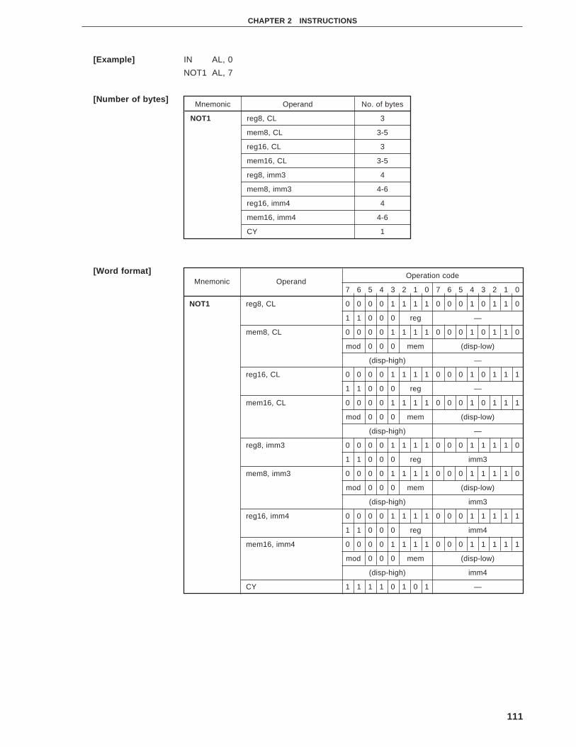
111
CHAPTER 2 INSTRUCTIONS
Mnemonic OperandOperation code
7 6 5 4 3 2 1 0 7 6 5 4 3 2 1 0
NOT1 reg8, CL 0 0 0 0 1 1 1 1 0 0 0 1 0 1 1 0
1 1 0 0 0 reg —
mem8, CL 0 0 0 0 1 1 1 1 0 0 0 1 0 1 1 0
mod 0 0 0 mem (disp-low)
(disp-high) —
reg16, CL 0 0 0 0 1 1 1 1 0 0 0 1 0 1 1 1
1 1 0 0 0 reg —
mem16, CL 0 0 0 0 1 1 1 1 0 0 0 1 0 1 1 1
mod 0 0 0 mem (disp-low)
(disp-high) —
reg8, imm3 0 0 0 0 1 1 1 1 0 0 0 1 1 1 1 0
1 1 0 0 0 reg imm3
mem8, imm3 0 0 0 0 1 1 1 1 0 0 0 1 1 1 1 0
mod 0 0 0 mem (disp-low)
(disp-high) imm3
reg16, imm4 0 0 0 0 1 1 1 1 0 0 0 1 1 1 1 1
1 1 0 0 0 reg imm4
mem16, imm4 0 0 0 0 1 1 1 1 0 0 0 1 1 1 1 1
mod 0 0 0 mem (disp-low)
(disp-high) imm4
CY 1 1 1 1 0 1 0 1 —
[Example] IN AL, 0
NOT1 AL, 7
[Number of bytes]
[Word format]
Mnemonic Operand No. of bytes
NOT1 reg8, CL 3
mem8, CL 3-5
reg16, CL 3
mem16, CL 3-5
reg8, imm3 4
mem8, imm3 4-6
reg16, imm4 4
mem16, imm4 4-6
CY 1

112
CHAPTER 2 INSTRUCTIONS
Logical sumOR Or
[Format] OR dst, src
[Operand, operation]
[Flag]
[Description] ORs the destination operand (dst) specified by the first operand with the source operand
(src) specified by the second operand, and stores the result to the destination operand
(dst).
[Example] OR AW, WORD PTR [IX]
[Number of bytes]
Mnemonic Operand (dst, src) Operation
OR reg, reg’ dst ← dst ∨ src
mem, reg
reg, mem
reg, imm
mem, imm
acc, imm [When W = 0] AL ← AL v imm8
[When W = 1] AW ← AW v imm16
AC CY V P S Z
U 0 0 × × ×
Mnemonic Operand No. of bytes
OR reg, reg’ 2
mem, reg 2-4
reg, mem 2-4
reg, imm 3, 4
mem, imm 3-6
acc, imm 2, 3

113
CHAPTER 2 INSTRUCTIONS
[Word format]
Note The following code may be generated depending on the assembler or compiler used.
Even in this case, the instruction is executed normally. Note, however, that some emulators
do not support a function to disassemble or assemble this instruction.
Mnemonic OperandOperation code
7 6 5 4 3 2 1 0 7 6 5 4 3 2 1 0
OR reg, reg’ 0 0 0 0 1 0 1 W 1 1 reg reg‘
mem, reg 0 0 0 0 1 0 0 W mod reg mem
(disp-low) (disp-high)
reg, mem 0 0 0 0 1 0 1 W mod reg mem
(disp-low) (disp-high)
reg, immNote 1 0 0 0 0 0 0 W 1 1 0 0 1 reg
imm8 or imm16-low imm16-high
mem, imm 1 0 0 0 0 0 0 W mod 0 0 1 mem
(disp-low) (disp-high)
imm8 or imm16-low imm16-high
acc, imm 0 0 0 0 1 1 0 W imm8 or imm16-low
imm16-high —
7 6 5 4 3 2 1 0 7 6 5 4 3 2 1 0
1 0 0 0 0 0 1 W 1 1 0 0 1 reg
imm8 —

114
CHAPTER 2 INSTRUCTIONS
Output data to I/O deviceOUTOutput
[Format] OUT dst, src
[Operand, operation]
[Flag]
[Description] Transfers the contents of the accumulator (AL or AW register) to a register of the I/O device
specified by the destination operand (dst).
[Example] To transfer contents of AL register to port address 0D8H
MOV DW, 0D8H
OUT DW, AL
[Number of bytes]
[Word format]
Mnemonic Operand (dst, src) Operation
OUT imm8, acc [When W = 0] (imm8) ← AL
[When W = 1] (imm8 + 1) ← AH, (imm8) ← AL
DW, acc [When W = 0] (DW) ← AL
[When W = 1] (DW + 1) ← AH, (DW) ← AL
AC CY V P S Z
Mnemonic Operand No. of bytes
OUT imm8, acc 2
DW, acc 1
Mnemonic OperandOperation code
7 6 5 4 3 2 1 0 7 6 5 4 3 2 1 0
OUT imm8, acc 1 1 1 0 0 1 1 W imm8
DW, acc 1 1 1 0 1 1 1 W —

115
CHAPTER 2 INSTRUCTIONS
Block transfer between memory and I/OOUTMOutput Multiple
[Format] (repeat) OUTM DW, [Seg-spec:] src-block
[Operation] [When W = 0] (DW) ← (IX)
DIR = 0: IX ← IX + 1
DIR = 1: IX ← IX – 1
[When W = 1] (DW + 1, DW) ← (IX + 1, IX)
DIR = 0: IX ← IX + 2
DIR = 1: IX ← IX – 2
[Operand]
[Flag]
[Description] Transfers the memory contents addressed by the IX register to the I/O device addressed
by the DW register. The number of times the data is repeatedly transferred is controlled
by the REP instruction, a repeat prefix used in pairs with this instruction. When the data
is repeatedly transferred, the contents of the DW register (address of the I/O device) are
fixed, but the value of the IX register is automatically incremented (+1/+2) or decremented
(–1/–2) to transfer the next byte/word each time 1-byte/word data has been transferred.
The direction of the block is determined by the status of the DIR flag.
Whether data is transferred in byte or word units is determined by the attribute of the
operand.
The OUTM instruction is used with a repeat prefix, REP instruction.
Although the default segment register of the source block is the DS0 register, segments
can be overridden, and the source block can be located in a segment specified by any
segment register.
[Example] • To transfer contents of memory 0:50H to port address 0D8H (byte data)
MOV AW, 0
MOV DS0, AW
MOV IX, 50H
MOV DW, 0D8H
OUTM DW, DS0: WORD PTR [IX]
• To transfer contents of memory 0:0H through 0FFH to port address 0D8H (byte data)
MOV AW, 0
MOV DS0, AW
MOV IX, 0H
MOV DW, 0D8H
MOV CW, 0FFH
REP OUTM DW, DS0:PTR [IX]
Mnemonic Operand
OUTM DW, [Seg-spec : ] src-block
AC CY V P S Z

116
CHAPTER 2 INSTRUCTIONS
[Number of bytes] 1
[Word format]Mnemonic Operand
Operation code
7 6 5 4 3 2 1 0
OUTM DW, [Seg-spec : ] src-block 0 1 1 0 1 1 1 W

117
CHAPTER 2 INSTRUCTIONS
Waits for floating-point coprocessorPOLLPoll and wait
[Format] POLL
[Operation] POLL and wait
[Operand]
[Flag]
[Description] • Other than V33A and V53A
Places the CPU in the wait status until the POLL pin becomes active (low).
Caution The BUSLOCK instruction must not be placed immediately before this
instruction.
• V33A and V53A
With coprocessor connected : Places the CPU in the wait status until the CPBUSY pin
becomes inactive (high level).
Without coprocessor : Generates coprocessor non-existent interrupt (vector
7). At this time, the first byte of this instruction is saved
to the stack as an address.
Caution The BUSLOCK instruction must not be placed immediately before this
instruction.
[Example] POLL
[Number of bytes] 1
[Word format]
AC CY V P S Z
Mnemonic Operand
POLL None
Mnemonic OperandOperation code
7 6 5 4 3 2 1 0
POLL None 1 0 0 1 1 0 1 1

118
CHAPTER 2 INSTRUCTIONS
Restore from stackPOPPop
[Word format] POP dst
[Operand, operation]
[Flag] • When dst = PSW
Remark The V33A and V53A does not have an MD flag.
• Other than above
[Description] Transfers the contents of the stack to the destination operand (dst) (however, the stack
contents are not transferred to the PS if dst = sreg).
Cautions 1. When dst = sreg, the hardware interrupt (maskable interrupt and non-
maskable interrupt) request and single-step break cannot be accepted
between this instruction and the next instruction.
2. When dst = PSW, the MD flag is restored only in the write- enabled
status, and is not affected in the write-disabled status (except the V33A
and V53A).
3. If the PUSH and POP instructions are executed to the SP register in
combination, the value of the SP register before instruction execution
minus 2 is stored to the SP register.
Mnemonic Operand (dst) Operation
POP mem16 SP ← SP + 2
(mem16) ← (SP – 1, SP – 2)
reg16 SP ← SP + 2
sreg dst ← (SP – 1, SP – 2)
PSW
R IY ← (SP + 1, SP)
IX ← (SP + 3, SP + 2)
BP ← (SP + 5, SP + 4)
BW ← (SP + 9, SP + 8)
DW ← (SP + 11, SP + 10)
CW ← (SP + 13, SP + 12)
AW ← (SP + 15, SP + 14)
SP ← SP + 16
AC CY V P S Z
AC CY V P S Z MD DIR IE BRK
R R R R R R R R R R

119
CHAPTER 2 INSTRUCTIONS
[Example] • POP AW
• POP BW
• POP IY
• POP SP
MOV BP, SP
[Number of bytes]
[Word format]
Mnemonic Operand No. of bytes
POP mem16 2-4
reg16 1
sreg
PSW
R 1
Mnemonic OperandOperation code
7 6 5 4 3 2 1 0 7 6 5 4 3 2 1 0
POP mem16 1 0 0 0 1 1 1 1 mod 0 0 0 mem
(disp-low) (disp-high)
reg16 0 1 0 1 1 reg —
sreg 0 0 0 sreg 1 1 1 —
PSW 1 0 0 1 1 1 0 1 —
R 0 1 1 0 0 0 0 1 —
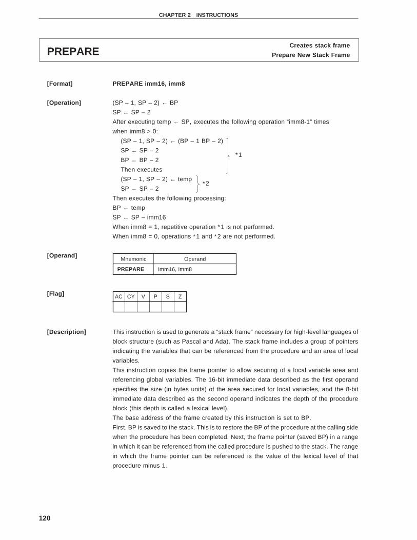
120
CHAPTER 2 INSTRUCTIONS
Mnemonic Operand
PREPARE imm16, imm8
AC CY V P S Z
Creates stack framePREPARE Prepare New Stack Frame
[Format] PREPARE imm16, imm8
[Operation] (SP – 1, SP – 2) ← BP
SP ← SP – 2
After executing temp ← SP, executes the following operation “imm8-1” times
when imm8 > 0:
(SP – 1, SP – 2) ← (BP – 1 BP – 2)
SP ← SP – 2∗1
BP ← BP – 2
Then executes
(SP – 1, SP – 2) ← temp∗2
SP ← SP – 2
Then executes the following processing:
BP ← temp
SP ← SP – imm16
When imm8 = 1, repetitive operation ∗1 is not performed.
When imm8 = 0, operations ∗1 and ∗2 are not performed.
[Operand]
[Flag]
[Description] This instruction is used to generate a “stack frame” necessary for high-level languages of
block structure (such as Pascal and Ada). The stack frame includes a group of pointers
indicating the variables that can be referenced from the procedure and an area of local
variables.
This instruction copies the frame pointer to allow securing of a local variable area and
referencing global variables. The 16-bit immediate data described as the first operand
specifies the size (in bytes units) of the area secured for local variables, and the 8-bit
immediate data described as the second operand indicates the depth of the procedure
block (this depth is called a lexical level).
The base address of the frame created by this instruction is set to BP.
First, BP is saved to the stack. This is to restore the BP of the procedure at the calling side
when the procedure has been completed. Next, the frame pointer (saved BP) in a range
in which it can be referenced from the called procedure is pushed to the stack. The range
in which the frame pointer can be referenced is the value of the lexical level of that
procedure minus 1.

121
CHAPTER 2 INSTRUCTIONS
If the lexical level is greater than 1, the frame pointer of this instruction itself is also pushed
to the stack. This is to copy the frame pointer of the procedure called by this procedure
when the called procedure copies the frame pointer.
Next, the value of a new frame pointer is set, and the area of local variables used for that
procedure are secured on the stack. In other words, the SP is decremented by the number
of the local variables.
[Example] MOV SP, 60H
MOV BP, SP
CALL CHK
PREPARE 0006, 04
MOV AW, [BP + 0FAH]
ADD AW, [BP + 0F8A]
MOV [BP + 0FCH], AW
[Number of Bytes] 4
[Word format]Mnemonic Operand
Operation code
7 6 5 4 3 2 1 0 7 6 5 4 3 2 1 0
PREPARE imm16, imm8 1 1 0 0 1 0 0 0 imm16-low
imm16-high imm8
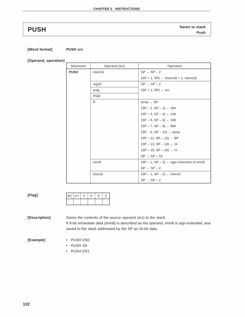
122
CHAPTER 2 INSTRUCTIONS
Saves to stackPUSHPush
[Word format] PUSH src
[Operand, operation]
[Flag]
[Description] Saves the contents of the source operand (src) to the stack.
If 8-bit immediate data (imm8) is described as the operand, imm8 is sign-extended, and
saved to the stack addressed by the SP as 16-bit data.
[Example] • PUSH DS0
• PUSH SS
• PUSH DS1
Mnemonic Operand (src) Operation
PUSH mem16 SP ← SP – 2
(SP + 1, SP) ← (mem16 + 1, mem16)
reg16 SP ← SP – 2
sreg (SP + 1, SP) ← src
PSW
R temp ← SP
(SP – 1, SP – 2) ← AW
(SP – 3, SP – 4) ← CW
(SP – 5, SP – 6) ← DW
(SP – 7, SP – 8) ← BW
(SP – 9, SP – 10) ← temp
(SP – 11, SP – 12) ← BP
(SP – 13, SP – 14) ← IX
(SP – 15, SP – 16) ← IY
SP ← SP – 16
imm8 (SP – 1, SP – 2) ← sign extension of imm8
SP ← SP – 2
imm16 (SP – 1, SP – 2) ← imm16
SP ← SP – 2
AC CY V P S Z

123
CHAPTER 2 INSTRUCTIONS
Mnemonic OperandOperation code
7 6 5 4 3 2 1 0 7 6 5 4 3 2 1 0
PUSH mem16 1 1 1 1 1 1 1 1 mod 1 1 0 mem
(disp-low) (disp-high)
reg16 0 1 0 1 0 reg —
sreg 0 0 0 sreg 1 1 0 —
PSW 1 0 0 1 1 1 0 0 —
R 0 1 1 0 0 0 0 0 —
imm8 0 1 1 0 1 0 1 0 imm8
imm16 0 1 1 0 1 0 0 0 imm16-low
imm16-high —
[Number of bytes]
[Word format]
Mnemonic Operand No. of bytes
PUSH mem16 2-4
reg16 1
sreg
PSW
R 1
imm8 2
imm16 3

124
CHAPTER 2 INSTRUCTIONS
Repeat prefix where Z = 1REPRepeatREPE Repeat while Equal
REPZ Repeat while Zero
[Format] REP
REPE
REPZ
[Operation] [When CW ≠ 0] PS: executes byte instruction of PC + 1
CW ← CW – 1
When Z ≠ 1: PC ← PC + 2
When Z = 1: Re-executes
[When CW = 0] PC ← PC + 2
[Operand]
[Flag]
[Description] Executes the block transfer/compare/I/O instruction of the subsequent byte and decrements
the value of CW register (–1) while CW ≠ 0.
REP is used in combination with the MOVBK, LDM, STM, OUTM, or INTM instruction, and
repeatedly performs processing while CW ≠ 0, regardless of the value of the Z flag.
REPZ and REPE are used in combination with the CMPBK or CMPM instruction, and exits
from a loop if Z ≠ 1 or if CW = 0 as a result of comparison by each block instruction. The
CW register is checked before the block compare instruction is executed, i.e., immediately
before the REP/REPE/REPEZ instruction is executed.
Therefore, if the REP/REPE/REPEZ instruction is executed when CW = 0, the subsequent
block compare instruction is never executed, and the next instruction is executed. The Z
flag is checked as a result of executing the subsequent block compare instruction, and the
content of this flag immediately before the REPE/REPZ instruction is executed for the first
time is irrelevant.
Caution The hardware interrupt (maskable interrupt) and non- maskable interrupt
request and single-step break cannot be accepted between this instruction
and the next instruction.
[Example] • REP MOVBKW
• REPZ CMPBKW
[Number of bytes] 1
Mnemonic Operand
REP None
REPE
REPZ
AC CY V P S Z

125
CHAPTER 2 INSTRUCTIONS
[Word format]Mnemonic Operand
Operation code
7 6 5 4 3 2 1 0
REP None 1 1 1 1 0 0 1 1
REPE
REPZ

126
CHAPTER 2 INSTRUCTIONS
Repeat prefix where CY = 1REPCRepeat while Carry
[Format] REPC
[Operation] [When CW ≠ 0] PS: executes byte instruction of PC + 1
CW ← CW – 1
When CY ≠ 1: PC ← PC + 2
When CY = 1: Re-executes
[When CW = 0] PC ← PC + 2
[Operand]
[Flag]
[Description] Executes the block compare (CMPBK or CMPM) instruction of the subsequent byte and
decrements the value of the CW register (–1) while CW ≠ 0.
If CY ≠ 1 as a result of executing the block compare instruction, execution exits from a loop.
The CW register is checked before the block compare instruction is executed, i.e.,
immediately before the REPC instruction is executed. Therefore, if the REPC instruction
is executed when CW = 0, the subsequent block compare instruction is never executed,
and the next instruction is executed.
The CY flag is checked as a result of executing the subsequent block compare instruction,
and the content of this flag immediately before the REPC instruction is executed for the
first time is irrelevant.
Caution The hardware interrupt (maskable interrupt) and non-maskable interrupt
request and single-step break cannot be accepted between this instruction
and the next instruction.
[Example] REPC CMPBKW
[Number of bytes] 1
[Word format]
Mnemonic Operand
REPC None
AC CY V P S Z
Mnemonic OperandOperation code
7 6 5 4 3 2 1 0
REPC None 0 1 1 0 0 1 0 1

127
CHAPTER 2 INSTRUCTIONS
Repeat prefix where CY = 0REPNCRepeat while Not Carry
[Format] REPNC
[Operation] [When CW ≠ 0] PS: executes byte instruction of PC + 1
CW ← CW – 1
When CY ≠ 1: Re-executes
When CY = 1: PC ← PC + 2
[When CW = 0] PC ← PC + 2
[Operand]
[Flag]
[Description] Executes the block compare (CMPBK or CMPM) instruction of the subsequent byte and
decrements the value of the CW register (–1) while CW ≠ 0.
If CY = 1 as a result of executing the block compare instruction, execution exits from a loop.
The CW register is checked before the block compare instruction is executed, i.e.,
immediately before the REPNC instruction is executed. Therefore, if the REPNC instruction
is executed when CW = 0, the subsequent block compare instruction is never executed,
and the next instruction is executed.
The CY flag is checked as a result of executing the subsequent block compare instruction,
and the content of this flag immediately before the REPNC instruction is executed for the
first time is irrelevant.
Caution The hardware interrupt (maskable interrupt) and non- maskable interrupt
request and single-step break cannot be accepted between this instruction
and the next instruction.
[Example] REPNC CMPMB
[Number of bytes] 1
[Word format]
Mnemonic Operand
REPNC None
AC CY V P S Z
Mnemonic OperandOperation code
7 6 5 4 3 2 1 0
REPNC None 0 1 1 0 0 1 0 0

128
CHAPTER 2 INSTRUCTIONS
Repeat prefix where Z = 0REPNERepeat while Not Equal
REPNZ Repeat while Not Zero
[Format] REPNE
REPNZ
[Operation] [When CW ≠ 0] PS: executes byte instruction of PC + 1
CW ← CW – 1
When Z ≠ 1: Re-executes
When Z = 1: PC ← PC + 2
[When CW = 0] PC ← PC + 2
[Operand]
[Flag]
[Description] Executes the block compare (CMPBK or CMPM) instruction of the subsequent byte and
decrements the value of the CW register (–1) while CW ≠ 0.
If Z ≠ 0 or if CW = 0 as a result of executing the block compare instruction, execution exits
from a loop.
The CW register is checked before the block compare instruction is executed, i.e.,
immediately before the REPNE/REPNZ instruction is executed. Therefore, if the REPNE/
REPNZ instruction is executed when CW = 0, the subsequent block compare instruction
is never executed, and the next instruction is executed.
The Z flag is checked as a result of executing the subsequent block compare instruction,
and the content of this flag immediately before the REPNC/REPNZ instruction is executed
for the first time is irrelevant.
Caution The hardware interrupt (maskable interrupt) and non-maskable interrupt
request and single-step break cannot be accepted between this instruction
and the next instruction.
[Example] • REPNE CMPMB
• REPNZ CMPBKW
[Number of bytes] 1
[Word format]
Mnemonic Operand
REPNE None
REPNZ
AC CY V P S Z
Mnemonic OperandOperation code
7 6 5 4 3 2 1 0
REPNE None 1 1 1 1 0 0 1 0
REPNZ
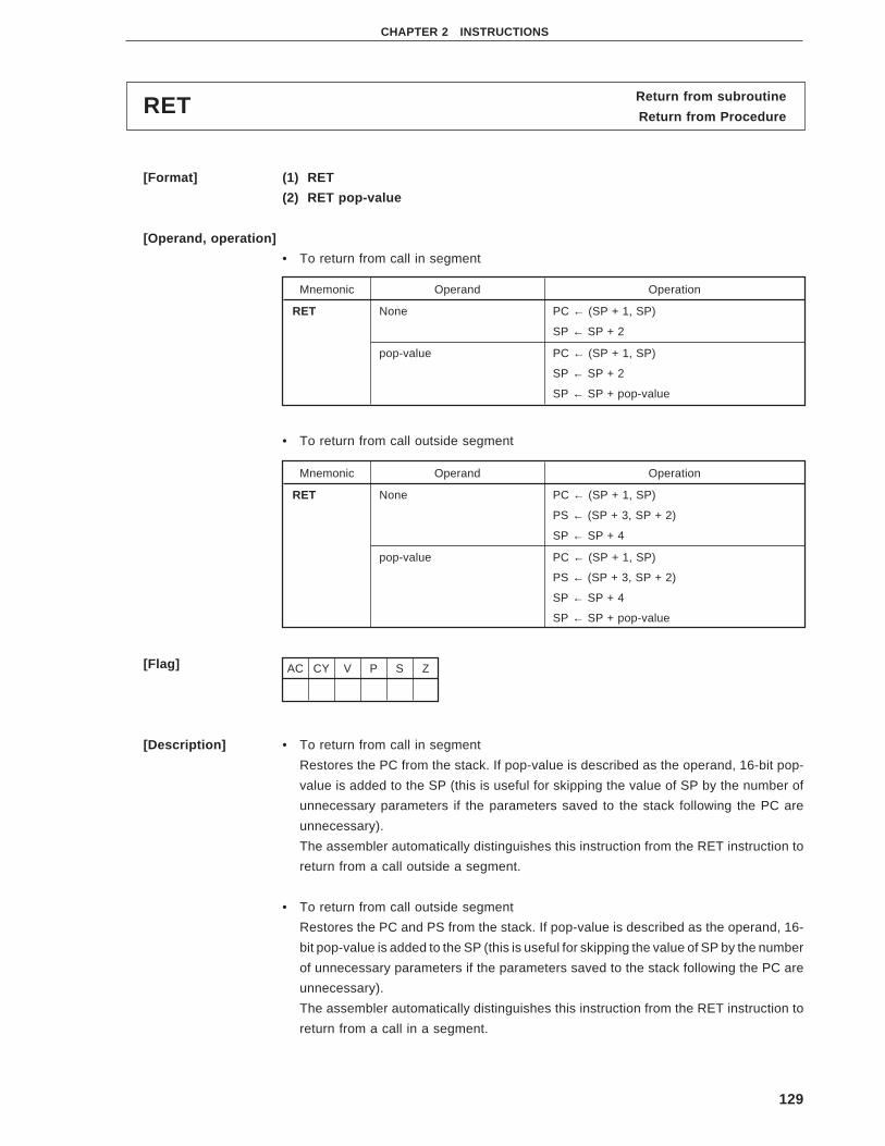
129
CHAPTER 2 INSTRUCTIONS
Return from subroutineRETReturn from Procedure
[Format] (1) RET
(2) RET pop-value
[Operand, operation]
• To return from call in segment
• To return from call outside segment
[Flag]
[Description] • To return from call in segment
Restores the PC from the stack. If pop-value is described as the operand, 16-bit pop-
value is added to the SP (this is useful for skipping the value of SP by the number of
unnecessary parameters if the parameters saved to the stack following the PC are
unnecessary).
The assembler automatically distinguishes this instruction from the RET instruction to
return from a call outside a segment.
• To return from call outside segment
Restores the PC and PS from the stack. If pop-value is described as the operand, 16-
bit pop-value is added to the SP (this is useful for skipping the value of SP by the number
of unnecessary parameters if the parameters saved to the stack following the PC are
unnecessary).
The assembler automatically distinguishes this instruction from the RET instruction to
return from a call in a segment.
Mnemonic Operand Operation
RET None PC ← (SP + 1, SP)
SP ← SP + 2
pop-value PC ← (SP + 1, SP)
SP ← SP + 2
SP ← SP + pop-value
Mnemonic Operand Operation
RET None PC ← (SP + 1, SP)
PS ← (SP + 3, SP + 2)
SP ← SP + 4
pop-value PC ← (SP + 1, SP)
PS ← (SP + 3, SP + 2)
SP ← SP + 4
SP ← SP + pop-value
AC CY V P S Z

130
CHAPTER 2 INSTRUCTIONS
[Example] POP R
RET
[Number of bytes]
[Word format] • To return from call in segment
• To return from call outside segment
Mnemonic Operand No. of bytes
RET None 1
pop-value 3
Mnemonic OperandOperation code
7 6 5 4 3 2 1 0 7 6 5 4 3 2 1 0
RET None 1 1 0 0 1 0 1 1 —
pop-value 1 1 0 0 1 0 1 0 pop-value-low
pop-value-high —
Mnemonic OperandOperation code
7 6 5 4 3 2 1 0 7 6 5 4 3 2 1 0
RET None 1 1 0 0 0 0 1 1 —
pop-value 1 1 0 0 0 0 1 0 pop-value-low
pop-value-high —

131
CHAPTER 2 INSTRUCTIONS
Return from emulation modeRETEM [except V33A and V53A]
Return from Emulation
[Format] RETEM
[Operation] PC ← (SP + 1, SP)
PS ← (SP + 3, SP + 2)
PSW ← (SP + 5, SP + 4)
SP ← SP + 6
Disables MD from being written.
[Operand]
[Flag]
[Description] When the RETEM instruction is executed in the emulation mode (this instruction is
interpreted as an instruction of the µPD8080AF), the CPU returns from interrupt service
to the native mode by restoring the PS, PC, and PSW that have been saved by the BRKEM
instruction. The content in the native mode saved by the BRKEM instruction (i.e., “1”) is
restored to the MD flag. As a result, the CPU enters the native mode. After the RETEM
instruction has been executed, the MD flag is disabled from being written, and cannot be
restored even if the RETI or POP PSW instruction is executed.
[Example] RETEM
[Number of bytes] 2
[Word format]
Mnemonic Operand
RETEM None
AC CY V P S Z MD DIR IE BRK
R R R R R R R R R R
Mnemonic OperandOperation code
7 6 5 4 3 2 1 0 7 6 5 4 3 2 1 0
RETEM None 1 1 1 0 1 1 0 1 1 1 1 1 1 1 0 1

132
CHAPTER 2 INSTRUCTIONS
Return from interruptRETIReturn from Interrupt
[Format] RETI
[Operation] PC ← (SP + 1, SP)
PS ← (SP + 3, SP + 2)
PSW ← (SP + 5, SP + 4)
SP ← SP + 6
[Operand]
[Flag]
Remark The V33A and V53A do not have an MD flag.
[Description] Restores the contents of the stack to the PC, PS, and PSW. This instruction is used to return
execution from interrupt service.
Caution The MD flag is restored only in the write-enabled status, and is not affected
in the write-disabled status (except the V33A and V53A).
[Example] POP R
RETI
[Number of bytes] 1
[Word format]
Mnemonic Operand
RETI None
AC CY V P S Z MD DIR IE BRK
R R R R R R R R R R
Mnemonic OperandOperation code
7 6 5 4 3 2 1 0
RETI None 1 1 0 0 1 1 1 1

133
CHAPTER 2 INSTRUCTIONS
Return from extended address modeRETXA [V33A, V53A only]
Return from Extended Address Mode
[Format] RETXA imm8
[Operation] temp1 ← (imm8 × 4 + 1, imm8 × 4)
temp2 ← (imm8 × 4 + 3, imm8 × 4 + 2)
XA ← 0
PC ← temp1
PS ← temp2
[Operand]
[Flag]
[Description] Releases the extended address mode.
Transfers control to the address stored in the entry of the interrupt vector table specified
by the instruction, and resets bit 0 (XA flag) of the XAM register (internal I/O address:
FF80H) to 0.
If this instruction is executed in the normal address mode, the vector table at the address
of the normal address mode is read and then execution jumps to the address of this vector
table.
If this instruction is executed in the extended address mode, the vector table at the address
of the extended address mode is read, the normal address mode is set, and then execution
jumps to the address read first.
The values of PC, PS, and PSW are not restored from the stack.
[Example] RETXA 0AH
[Number of bytes] 3
[Word format]
Mnemonic Operand
RETXA imm8
AC CY V P S Z
Mnemonic OperandOperation code
7 6 5 4 3 2 1 0 7 6 5 4 3 2 1 0
RETXA imm8 0 0 0 0 1 1 1 1 1 1 1 1 0 0 0 0
imm8 —

134
CHAPTER 2 INSTRUCTIONS
Rotate leftROLRotate Left
[Format] ROL dst, src
[Operation]
[Operand]
[Flag] When src = 1 Others
[Description] • When src = 1
Shifts the contents of the destination operand (dst) specified by the first operand 1 bit
to the left. The data of the MSB (bit 7 or 15) of dst is shifted to the LSB (bit 0) position,
and is also transferred to the CY flag. If the MSB is affected, the V flag is set to 1; if
not, the V flag is reset to 0.
• When src = CL or src = imm8
Shifts the contents of the destination operand (dst) specified by the first operand to the
left the number of bits of the contents of the source operand (src) specified by the second
operand. The data of the MSB (bit 7 or 15) of dst is shifted to the LSB (bit 0) position,
and is also transferred to the CY flag.
[Example] MOV [IX], BL
ROL BYTE PTR [IX], 1
[Number of bytes]
Mnemonic Operand (dst, src)
ROL reg, 1
mem, 1
reg, CL
mem, CL
reg, imm8
mem, imm8
AC CY V P S Z
× ×
AC CY V P S Z
× U
Mnemonic Operand No. of bytes
ROL reg, 1 2
mem, 1 2-4
reg, CL 2
mem, CL 2-4
reg, imm8 3
mem, imm8 3-5
CY 15/7 0
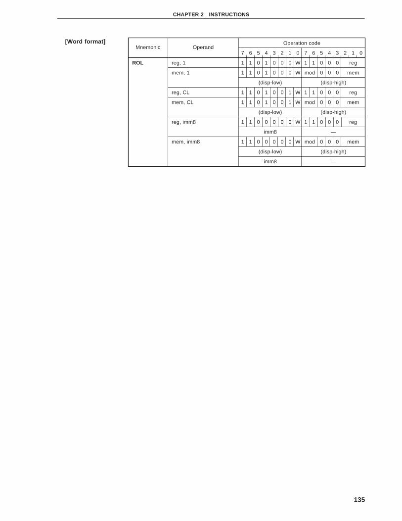
135
CHAPTER 2 INSTRUCTIONS
[Word format]Mnemonic Operand
Operation code
7 6 5 4 3 2 1 0 7 6 5 4 3 2 1 0
ROL reg, 1 1 1 0 1 0 0 0 W 1 1 0 0 0 reg
mem, 1 1 1 0 1 0 0 0 W mod 0 0 0 mem
(disp-low) (disp-high)
reg, CL 1 1 0 1 0 0 1 W 1 1 0 0 0 reg
mem, CL 1 1 0 1 0 0 1 W mod 0 0 0 mem
(disp-low) (disp-high)
reg, imm8 1 1 0 0 0 0 0 W 1 1 0 0 0 reg
imm8 —
mem, imm8 1 1 0 0 0 0 0 W mod 0 0 0 mem
(disp-low) (disp-high)
imm8 —
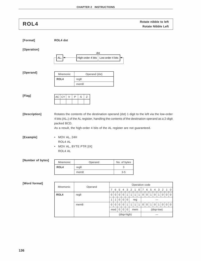
136
CHAPTER 2 INSTRUCTIONS
Rotate nibble to leftROL4Rotate Nibble Left
[Format] ROL4 dst
[Operation]
[Operand]
[Flag]
[Description] Rotates the contents of the destination operand (dst) 1 digit to the left via the low-order
4 bits (ALL) of the AL register, handling the contents of the destination operand as a 2-digit
packed BCD.
As a result, the high-order 4 bits of the AL register are not guaranteed.
[Example] • MOV AL, 24H
ROL4 AL
• MOV AL, BYTE PTR [IX]
ROL4 AL
[Number of bytes]
[Word format]
Mnemonic Operand (dst)
ROL4 reg8
mem8
AC CY V P S Z
Mnemonic Operand No. of bytes
ROL4 reg8 3
mem8 3-5
Mnemonic OperandOperation code
7 6 5 4 3 2 1 0 7 6 5 4 3 2 1 0
ROL4 reg8 0 0 0 0 1 1 1 1 0 0 1 0 1 0 0 0
1 1 0 0 0 reg —
mem8 0 0 0 0 1 1 1 1 0 0 1 0 1 0 0 0
mod 0 0 0 mem (disp-low)
(disp-high) —
dst
High-order 4 bits Low-order 4 bitsALL

137
CHAPTER 2 INSTRUCTIONS
Rotate left with carryROLCRotate Left with Carry
[Format] ROLC dst, src
[Operation]
[Operand]
[Flag] When src = 1 Others
[Description] • When src = 1
Shifts the contents of the destination operand (dst) specified by the first operand 1 bit
to the left via the CY flag. The data of the MSB (bit 7 or 15) of dst is transferred to the
CY flag, and the data of the CY flag is transferred to the LSB (bit 0). If the MSB is affected,
the V flag is set to 1; if not, the V flag is reset to 0.
• When src = CL or src = imm8
Shifts the contents of the destination operand (dst) specified by the first operand to the
left the number of bits of the contents of the source operand (src) specified by the second
operand via the CY flag. The data of the MSB (bit 7 or 15) of dst is transferred to the
CY flag, and the data of the CY flag is transferred to the LSB (bit 0).
[Example] • ROLC AL, 1
• ROLC CL, 1
• ROLC DW, 1
• ROLC AW, 1
Mnemonic Operand (dst, src)
ROLC reg, 1
mem, 1
reg, CL
mem, CL
reg, imm8
mem, imm8
AC CY V P S Z
× ×
AC CY V P S Z
× U
CY 15/7 0

138
CHAPTER 2 INSTRUCTIONS
[Number of bytes]
[Word format]
Mnemonic Operand No. of bytes
ROLC reg, 1 2
mem, 1 2-4
reg, CL 2
mem, CL 2-4
reg, imm8 3
mem, imm8 3-5
Mnemonic OperandOperation code
7 6 5 4 3 2 1 0 7 6 5 4 3 2 1 0
ROLC reg, 1 1 1 0 1 0 0 0 W 1 1 0 1 0 reg
mem, 1 1 1 0 1 0 0 0 W mod 0 1 0 mem
(disp-low) (disp-high)
reg, CL 1 1 0 1 0 0 1 W 1 1 0 1 0 reg
mem, CL 1 1 0 1 0 0 1 W mod 0 1 0 mem
(disp-low) (disp-high)
reg, imm8 1 1 0 0 0 0 0 W 1 1 0 1 0 reg
imm8 —
mem, imm8 1 1 0 0 0 0 0 W mod 0 1 0 mem
(disp-low) (disp-high)
imm8 —

139
CHAPTER 2 INSTRUCTIONS
Rotate rightRORRotate Right
[Format] ROR dst, src
[Operation]
[Operand]
[Flag] When src = 1 Others
[Description] • When src = 1
Shifts the contents of the destination operand (dst) specified by the first operand 1 bit
to the right. The data of the LSB (bit 0) of dst is shifted to the MSB (bit 7 or 15) position,
and is also transferred to the CY flag. If the MSB is affected, the V flag is set to 1; if
not, the V flag is reset to 0.
• When src = CL or src = imm8
Shifts the contents of the destination operand (dst) specified by the first operand to the
right the number of bits of the contents of the source operand (src) specified by the
second operand. The data of the LSB (bit 0) of dst is shifted to the MSB (bit 7 or 15)
position, and is also transferred to the CY flag.
[Example] • ROR AL, 3
• ROR CW, 6
• ROR IY, 2
Mnemonic Operand (dst, src)
ROR reg, 1
mem, 1
reg, CL
mem, CL
reg, imm8
mem, imm8
AC CY V P S Z
× ×
AC CY V P S Z
× U
CY 15/7 0
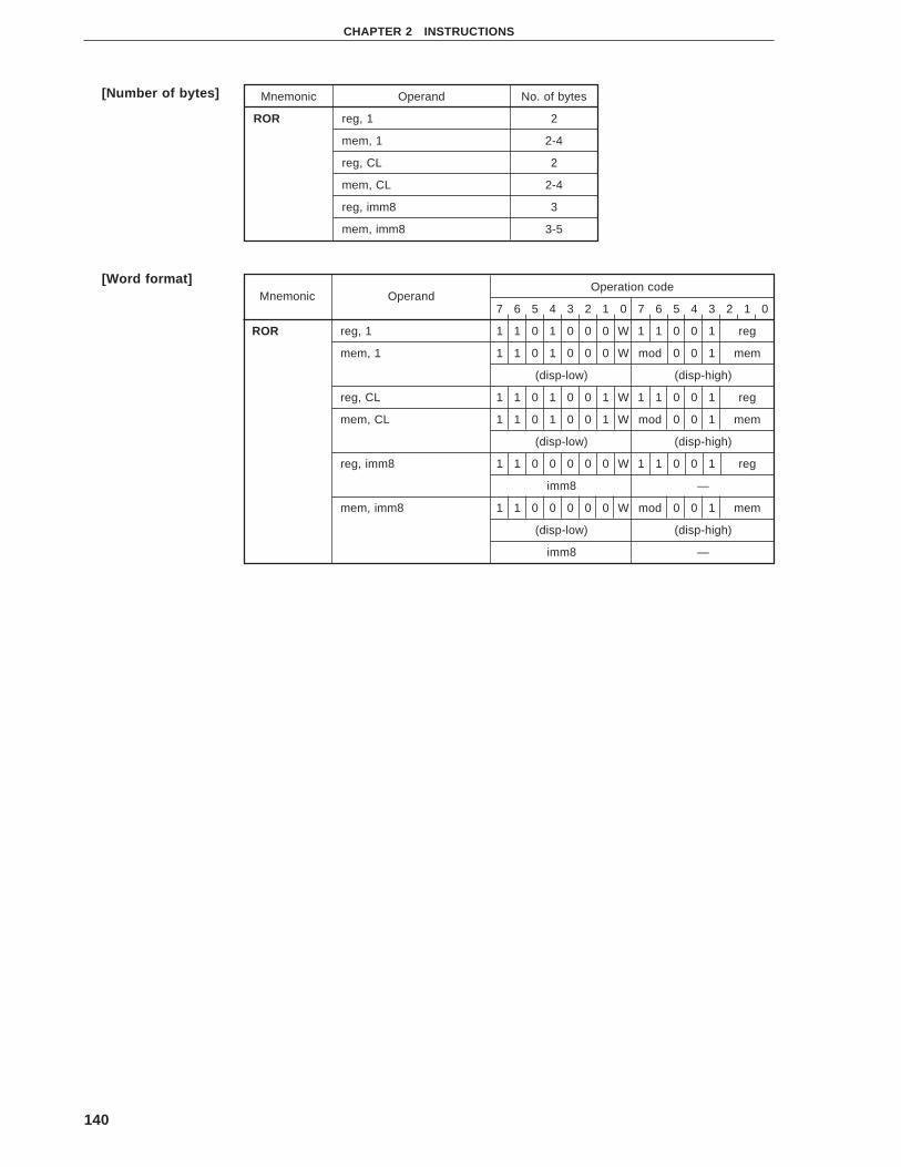
140
CHAPTER 2 INSTRUCTIONS
[Number of bytes]
[Word format]
Mnemonic Operand No. of bytes
ROR reg, 1 2
mem, 1 2-4
reg, CL 2
mem, CL 2-4
reg, imm8 3
mem, imm8 3-5
Mnemonic OperandOperation code
7 6 5 4 3 2 1 0 7 6 5 4 3 2 1 0
ROR reg, 1 1 1 0 1 0 0 0 W 1 1 0 0 1 reg
mem, 1 1 1 0 1 0 0 0 W mod 0 0 1 mem
(disp-low) (disp-high)
reg, CL 1 1 0 1 0 0 1 W 1 1 0 0 1 reg
mem, CL 1 1 0 1 0 0 1 W mod 0 0 1 mem
(disp-low) (disp-high)
reg, imm8 1 1 0 0 0 0 0 W 1 1 0 0 1 reg
imm8 —
mem, imm8 1 1 0 0 0 0 0 W mod 0 0 1 mem
(disp-low) (disp-high)
imm8 —
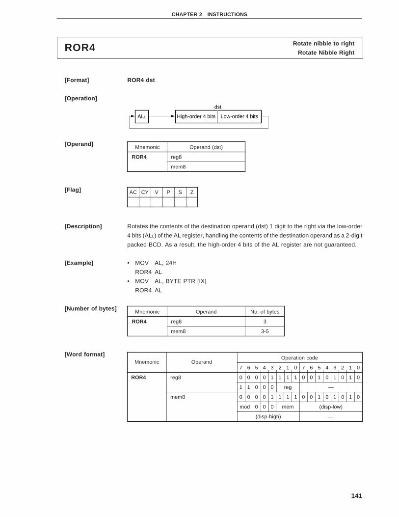
141
CHAPTER 2 INSTRUCTIONS
Rotate nibble to rightROR4Rotate Nibble Right
[Format] ROR4 dst
[Operation]
[Operand]
[Flag]
[Description] Rotates the contents of the destination operand (dst) 1 digit to the right via the low-order
4 bits (ALL) of the AL register, handling the contents of the destination operand as a 2-digit
packed BCD. As a result, the high-order 4 bits of the AL register are not guaranteed.
[Example] • MOV AL, 24H
ROR4 AL
• MOV AL, BYTE PTR [IX]
ROR4 AL
[Number of bytes]
[Word format]
Mnemonic Operand (dst)
ROR4 reg8
mem8
AC CY V P S Z
Mnemonic Operand No. of bytes
ROR4 reg8 3
mem8 3-5
Mnemonic OperandOperation code
7 6 5 4 3 2 1 0 7 6 5 4 3 2 1 0
ROR4 reg8 0 0 0 0 1 1 1 1 0 0 1 0 1 0 1 0
1 1 0 0 0 reg —
mem8 0 0 0 0 1 1 1 1 0 0 1 0 1 0 1 0
mod 0 0 0 mem (disp-low)
(disp-high) —
dst
High-order 4 bits Low-order 4 bitsALL

142
CHAPTER 2 INSTRUCTIONS
Rotate right with carryRORCRotate Right with Carry
[Format] RORC dst, src
[Operation]
[Operand]
[Flag] When src = 1 Others
[Description] • When src = 1
Shifts the contents of the destination operand (dst) specified by the first operand 1 bit
to the right via the CY flag. The data of the LSB (bit 0) of dst is transferred to the CY
flag, and the data of the CY flag is transferred to the LSB (bit 7 or 15). If the MSB is
affected, the V flag is set to 1; if not, the V flag is reset to 0.
• When src = CL or src = imm8
Shifts the contents of the destination operand (dst) specified by the first operand to the
right by the number of bits of the contents of the source operand (src) specified by the
second operand via the CY flag. The data of the LSB (bit 0) of dst is transferred to the
CY flag, and the data of the CY flag is transferred to the MSB (bit 7 or 15).
[Example] • RORC AL, 1
• RORC BL, 1
• RORC CW, 1
• RORC IX, 1
Mnemonic Operand (dst, src)
RORC reg, 1
mem, 1
reg, CL
mem, CL
reg, imm8
mem, imm8
AC CY V P S Z
× ×
AC CY V P S Z
× U
CY 15/7 0

143
CHAPTER 2 INSTRUCTIONS
[Number of bytes]
[Word format]
Mnemonic Operand No. of bytes
RORC reg, 1 2
mem, 1 2-4
reg, CL 2
mem, CL 2-4
reg, imm8 3
mem, imm8 3-5
Mnemonic OperandOperation code
7 6 5 4 3 2 1 0 7 6 5 4 3 2 1 0
RORC reg, 1 1 1 0 1 0 0 0 W 1 1 0 1 1 reg
mem, 1 1 1 0 1 0 0 0 W mod 0 1 1 mem
(disp-low) (disp-high)
reg, CL 1 1 0 1 0 0 1 W 1 1 0 1 1 reg
mem, CL 1 1 0 1 0 0 1 W mod 0 1 1 mem
(disp-low) (disp-high)
reg, imm8 1 1 0 0 0 0 0 W 1 1 0 1 1 reg
imm8 —
mem, imm8 1 1 0 0 0 0 0 W mod 0 1 1 mem
(disp-low) (disp-high)
imm8 —
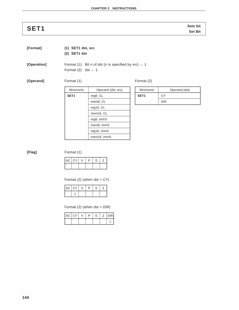
144
CHAPTER 2 INSTRUCTIONS
Sets bitSET1Set Bit
[Format] (1) SET1 dst, src
(2) SET1 dst
[Operation] Format (1): Bit n of dst (n is specified by src) ← 1
Format (2): dst ← 1
[Operand] Format (1) Format (2)
[Flag] Format (1)
Format (2) (when dst = CY)
Format (2) (when dst = DIR)
Mnemonic Operand (dst, src)
SET1 reg8, CL
mem8, CL
reg16, CL
mem16, CL
reg8, imm3
mem8, imm3
reg16, imm4
mem16, imm4
Mnemonic Operand (dst)
SET1 CY
DIR
AC CY V P S Z
AC CY V P S Z
1
AC CY V P S Z DIR
1

145
CHAPTER 2 INSTRUCTIONS
[Description] Format (1): Sets bit n (n is the contents of the source operand (src) specified by the
second operand) of the destination operand (dst) specified by the first
operand to 1, and stores the result to the destination operand (dst).
If the operand is reg8, CL or mem8, CL, only the low-order 3 bits of the value
of CL (0 to 7) are valid. If the operand is reg16, CL or mem16, CL, only the
low-order 4 bits of the value of CL (0 to 15) are valid.
If the operand is reg8, imm3, only the low-order 3 bits of the immediate data
at the fourth byte position of the instruction are valid.
If the operand is mem8, imm3, only the low-order 3 bits of the immediate data
at the last byte position of the instruction are valid.
If the operand is reg16, imm4, only the low-order 4 bits of the immediate data
at the fourth byte position of the instruction are valid.
If the operand is mem16, imm4, only the low-order 4 bits of the immediate
data at the last byte position of the instruction are valid.
Format (2): When dst = CY, sets the CY flag to 1.
When dst = DIR, sets the DIR flag to 1. Also sets so that the index registers
(IX and IY) are auto-decremented when the MOVBK, CMPBK, CMPM, LDM,
STM, INM, or OUTM instruction is executed.
[Example] MOV CL, 4
SET1 AL, CL
OUT 0DAH, AL
[Number of bytes]Mnemonic Operand No. of bytes
SET1 reg8, CL 3
mem8, CL 3-5
reg16, CL 3
mem16, CL 3-5
reg8, imm3 4
mem8, imm3 4-6
reg16, imm4 4
mem16, imm4 4-6
CY 1
DIR 1

146
CHAPTER 2 INSTRUCTIONS
[Word format]Mnemonic Operand
Operation code
7 6 5 4 3 2 1 0 7 6 5 4 3 2 1 0
SET1 reg8, CL 0 0 0 0 1 1 1 1 0 0 0 1 0 1 0 0
1 1 0 0 0 reg —
mem8, CL 0 0 0 0 1 1 1 1 0 0 0 1 0 1 0 0
mod 0 0 0 mem (disp-low)
(disp-high) —
reg16, CL 0 0 0 0 1 1 1 1 0 0 0 1 0 1 0 1
1 1 0 0 0 reg —
mem16, CL 0 0 0 0 1 1 1 1 0 0 0 1 0 1 0 1
mod 0 0 0 mem (disp-low)
(disp-high) —
reg8, imm3 0 0 0 0 1 1 1 1 0 0 0 1 1 1 0 0
1 1 0 0 0 reg imm3
mem8, imm3 0 0 0 0 1 1 1 1 0 0 0 1 1 1 0 0
mod 0 0 0 mem (disp-low)
(disp-high) imm3
rg16, imm4 0 0 0 0 1 1 1 1 0 0 0 1 1 1 0 1
1 1 0 0 0 reg imm4
mem16, imm4 0 0 0 0 1 1 1 1 0 0 0 1 1 1 0 1
mod 0 0 0 mem (disp-low)
(disp-high) imm4
CY 1 1 1 1 1 0 0 1 —
DIR 1 1 1 1 1 1 0 1 —

147
CHAPTER 2 INSTRUCTIONS
Shift leftSHLShift Left
[Format] SHL dst, src
[Operation]
[Operand]
[Flag] When src = 1 Others
[Description] • When src = 1
Shifts the contents of the destination operand (dst) specified by the first operand 1 bit
to the left. Zero is shifted in to the the LSB (bit 0) position of dst, and the data of the
MSB (bit 7 or 15) is set to the CY flag. The V flag is cleared if the sign bit (bit 7 or 15)
is not affected after shifting.
• When src = CL or src = imm8
Shifts the contents of the destination operand (dst) specified by the first operand to the
left the number of bits of the contents of the source operand (src) specified by the second
operand. Zero is shifted in to the LSB (bit 0) position of dst each time the data is shifted,
and the data of the MSB (bit 7 or 15) is set to the CY flag.
[Example] IN AW, 0C8H
MOV [IY], AW
SHL WORD PTR [IY], 12
Mnemonic Operand (dst, src)
SHL reg, 1
mem, 1
reg, CL
mem, CL
reg, imm8
mem, imm8
AC CY V P S Z
U × × × × ×
AC CY V P S Z
U × U × × ×
CY 15/7 0
0

148
CHAPTER 2 INSTRUCTIONS
[Number of bytes]
[Word format]
Mnemonic Operand No. of bytes
SHL reg, 1 2
mem, 1 2-4
reg, CL 2
mem, CL 2-4
reg, imm8 3
mem, imm8 3-5
Mnemonic OperandOperation code
7 6 5 4 3 2 1 0 7 6 5 4 3 2 1 0
SHL reg, 1 1 1 0 1 0 0 0 W 1 1 1 0 0 reg
mem, 1 1 1 0 1 0 0 0 W mod 1 0 0 mem
(disp-low) (disp-high)
reg, CL 1 1 0 1 0 0 1 W 1 1 1 0 0 reg
mem, CL 1 1 0 1 0 0 1 W mod 1 0 0 mem
(disp-low) (disp-high)
reg, imm8 1 1 0 0 0 0 0 W 1 1 1 0 0 reg
imm8 —
mem, imm8 1 1 0 0 0 0 0 W mod 1 0 0 mem
(disp-low) (disp-high)
imm8 —

149
CHAPTER 2 INSTRUCTIONS
Shift rightSHRShift Right
[Format] SHR dst, src
[Operation]
[Operand]
[Flag] When src = 1 Others
[Description] • When src = 1
Shifts the contents of the destination operand (dst) specified by the first operand 1 bit
to the right. Zero is shifted in to the the MSB (bit 7 or 15) position of dst, and the data
of the LSB (bit 0) is set to the CY flag. The V flag is cleared if the sign bit (bit 7 or 15)
is not affected after shifting.
• When src = CL or src = imm8
Shifts the contents of the destination operand (dst) specified by the first operand to the
right the number of bits of the contents of the source operand (src) specified by the
second operand. Zero is shifted in to the MSB (bit 7 or 15) position of dst each time the
data is shifted, and the data of the LSB (bit 0) is set to the CY flag.
[Example] • RCV: IN AL, 0DAH
SHR AL, 3
BC RCV
• SHR CW, 8
Mnemonic Operand (dst, src)
SHR reg, 1
mem, 1
reg, CL
mem, CL
reg, imm8
mem, imm8
AC CY V P S Z
U × × × × ×
AC CY V P S Z
U × U × × ×
CY 15/7 0
0

150
CHAPTER 2 INSTRUCTIONS
[Number of bytes]
[Word format]
Mnemonic Operand No. of bytes
SHR reg, 1 2
mem, 1 2-4
reg, CL 2
mem, CL 2-4
reg, imm8 3
mem, imm8 3-5
Mnemonic OperandOperation code
7 6 5 4 3 2 1 0 7 6 5 4 3 2 1 0
SHR reg, 1 1 1 0 1 0 0 0 W 1 1 1 0 1 reg
mem, 1 1 1 0 1 0 0 0 W mod 1 0 1 mem
(disp-low) (disp-high)
reg, CL 1 1 0 1 0 0 1 W 1 1 1 0 1 reg
mem, CL 1 1 0 1 0 0 1 W mod 1 0 1 mem
(disp-low) (disp-high)
reg, imm8 1 1 0 0 0 0 0 W 1 1 1 0 1 reg
imm8 —
mem, imm8 1 1 0 0 0 0 0 W mod 1 0 1 mem
(disp-low) (disp-high)
imm8 —

151
CHAPTER 2 INSTRUCTIONS
Arithmetic shift rightSHRAShift Right Arithmetic
[Format] SHRA dst, src
[Operation]
[Operand]
[Flag] When src = 1 Others
[Description] • When src = 1
Arithmetically shifts the contents of the destination operand (dst) specified by the first
operand 1 bit to the right. The original value is shifted in to the the MSB (bit 7 or 15)
position of dst, and the sign is not affected after shifting. The data of the LSB (bit 0) is
set to the CY flag.
• When src = CL or src = imm8
Shifts the contents of the destination operand (dst) specified by the first operand to the
right the number of bits of the contents of the source operand (src) specified by the
second operand. The original value is shifted in to the MSB (bit 7 or 15) of dst, and the
sign is not affected after shifting. The data of the LSB (bit 0) is set to the CY flag.
[Example] • MOV CL, 2
SHRA BL, CL
• MOV CL, 9
SHRA DW, CL
Mnemonic Operand (dst, src)
SHRA reg, 1
mem, 1
reg, CL
mem, CL
reg, imm8
mem, imm8
AC CY V P S Z
U × 0 × × ×
AC CY V P S Z
U × U × × ×
CY 15/7 0

152
CHAPTER 2 INSTRUCTIONS
[Number of bytes]
[Word format]
Mnemonic Operand No. of bytes
SHRA reg, 1 2
mem, 1 2-4
reg, CL 2
mem, CL 2-4
reg, imm8 3
mem, imm8 3-5
Mnemonic OperandOperation code
7 6 5 4 3 2 1 0 7 6 5 4 3 2 1 0
SHRA reg, 1 1 1 0 1 0 0 0 W 1 1 1 1 1 reg
mem, 1 1 1 0 1 0 0 0 W mod 1 1 1 mem
(disp-low) (disp-high)
reg, CL 1 1 0 1 0 0 1 W 1 1 1 1 1 reg
mem, CL 1 1 0 1 0 0 1 W mod 1 1 1 mem
(disp-low) (disp-high)
reg, imm8 1 1 0 0 0 0 0 W 1 1 1 1 1 reg
imm8 —
mem, imm8 1 1 0 0 0 0 0 W mod 1 1 1 mem
(disp-low) (disp-high)
imm8 —
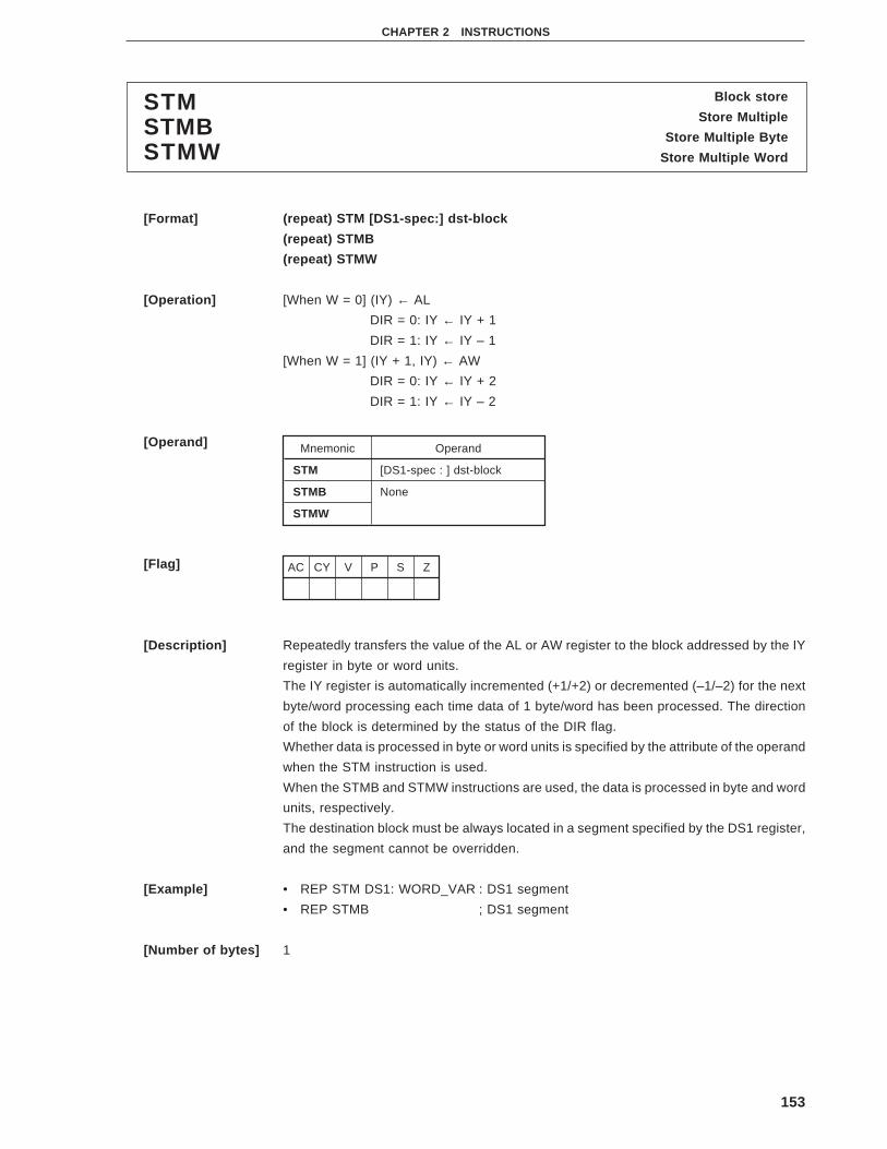
153
CHAPTER 2 INSTRUCTIONS
Block storeSTMStore MultipleSTMB Store Multiple Byte
STMW Store Multiple Word
[Format] (repeat) STM [DS1-spec:] dst-block
(repeat) STMB
(repeat) STMW
[Operation] [When W = 0] (IY) ← AL
DIR = 0: IY ← IY + 1
DIR = 1: IY ← IY – 1
[When W = 1] (IY + 1, IY) ← AW
DIR = 0: IY ← IY + 2
DIR = 1: IY ← IY – 2
[Operand]
[Flag]
[Description] Repeatedly transfers the value of the AL or AW register to the block addressed by the IY
register in byte or word units.
The IY register is automatically incremented (+1/+2) or decremented (–1/–2) for the next
byte/word processing each time data of 1 byte/word has been processed. The direction
of the block is determined by the status of the DIR flag.
Whether data is processed in byte or word units is specified by the attribute of the operand
when the STM instruction is used.
When the STMB and STMW instructions are used, the data is processed in byte and word
units, respectively.
The destination block must be always located in a segment specified by the DS1 register,
and the segment cannot be overridden.
[Example] • REP STM DS1: WORD_VAR : DS1 segment
• REP STMB ; DS1 segment
[Number of bytes] 1
Mnemonic Operand
STM [DS1-spec : ] dst-block
STMB None
STMW
AC CY V P S Z

154
CHAPTER 2 INSTRUCTIONS
[Word format]Mnemonic Operand
Operation code
7 6 5 4 3 2 1 0
STM [DS1-spec : ] dst-block 1 0 1 0 1 0 1 W
STMB None
STMW

155
CHAPTER 2 INSTRUCTIONS
SubtractSUBSubtract
[Format] SUB dst, src
[Operand, Operation]
[Flag]
[Description] Subtracts the contents of the source operand (src) specified by the second operand from
the contents of the destination operand (dst) specified by the first operand, and stores the
result to the destination operand (dst).
[Example] To subtract contents of memory 0:50H from contents of DL register, and store result to DL
register
MOV AW, 0
MOV DS0, AW
MOV IX, 50H
SUB DL, DS0:BYTE PTR [IX]
[Number of bytes]
Mnemonic Operand (dst, src) Operation
SUB reg, reg’ dst ← dst – src
mem, reg
reg, mem
reg, imm
mem, imm
acc, imm [When W = 0] AL ← AL – imm8
[When W = 1] AW ← AW – imm16
AC CY V P S Z
× × × × × ×
Mnemonic Operand No. of bytes
SUB reg, reg’ 2
mem, reg 2-4
reg, mem 2-4
reg, imm 3, 4
mem, imm 3-6
acc, imm 2, 3

156
CHAPTER 2 INSTRUCTIONS
[Word format]Mnemonic Operand
Operation code
7 6 5 4 3 2 1 0 7 6 5 4 3 2 1 0
SUB reg, reg’ 0 0 1 0 1 0 1 W 1 1 reg reg‘
mem, reg 0 0 1 0 1 0 0 W mod reg mem
(disp-low) (disp-high)
reg, mem 0 0 1 0 1 0 1 W mod reg mem
(disp-low) (disp-high)
reg, imm 1 0 0 0 0 0 s W 1 1 1 0 1 reg
imm8 or imm16-low imm16-high
mem, imm 1 0 0 0 0 0 s W mod 1 0 1 mem
(disp-low) (disp-high)
imm8 or imm16-low imm16-high
acc, imm 0 0 1 0 1 1 0 W imm8 or imm16-low
imm16-high —
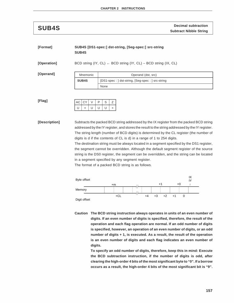
157
CHAPTER 2 INSTRUCTIONS
Decimal subtractionSUB4SSubtract Nibble String
[Format] SUB4S [DS1-spec:] dst-string, [Seg-spec:] src-string
SUB4S
[Operation] BCD string (IY, CL) ← BCD string (IY, CL) – BCD string (IX, CL)
[Operand]
[Flag]
[Description] Subtracts the packed BCD string addressed by the IX register from the packed BCD string
addressed by the IY register, and stores the result to the string addressed by the IY register.
The string length (number of BCD digits) is determined by the CL register (the number of
digits is d if the contents of CL is d) in a range of 1 to 254 digits.
The destination string must be always located in a segment specified by the DS1 register,
the segment cannot be overridden. Although the default segment register of the source
string is the DS0 register, the segment can be overridden, and the string can be located
in a segment specified by any segment register.
The format of a packed BCD string is as follows.
Caution The BCD string instruction always operates in units of an even number of
digits. If an even number of digits is specified, therefore, the result of the
operation and each flag operation are normal. If an odd number of digits
is specified, however, an operation of an even number of digits, or an odd
number of digits + 1, is executed. As a result, the result of the operation
is an even number of digits and each flag indicates an even number of
digits.
To specify an odd number of digits, therefore, keep this in mind: Execute
the BCD subtraction instruction, if the number of digits is odd, after
clearing the high-order 4 bits of the most significant byte to “0”. If a borrow
occurs as a result, the high-order 4 bits of the most significant bit is “9”.
Mnemonic Operand (dst, src)
SUB4S [DS1-spec : ] dst-string, [Seg-spec : ] src-string
None
AC CY V P S Z
U × U U U ×
Memory
Byte offset
Digit offset
+m
+CL 0+1+2+3+4
+0+1
IXIY↓

158
CHAPTER 2 INSTRUCTIONS
[Example] MOV IX, OFFSET VAR_1
MOV IY, OFFSET VAR_2
MOV CL, 4
SUB4S
[Number of bytes] 2
[Word format]
Mnemonic OperandOperation code
7 6 5 4 3 2 1 0 7 6 5 4 3 2 1 0
SUB4S [DS1-spec : ] dst-string, [Seg-spec : ] src-string 0 0 0 0 1 1 1 1 0 0 1 0 0 0 1 0
None

159
CHAPTER 2 INSTRUCTIONS
Subtraction with carrySUBCSubtract with Carry
[Format] SUBC dst, src
[Operand, Operation]
[Flag]
[Description] Subtracts the contents of the source operand (src) specified by the second operand from
the contents of the destination operand (dst) specified by the first operand, and stores the
result to the destination operand (dst).
[Example] SUBC DL, BYTE PTR [IX]
[Number of bytes]
Mnemonic Operand (dst, src) Operation
SUBC reg, reg’ dst ← dst – src – CY
mem, reg
reg, mem
reg, imm
mem, imm
acc, imm [When W = 0] AL ← AL + imm8 – CY
[When W = 1] AW ← AW – imm16 – CY
AC CY V P S Z
× × × × × ×
Mnemonic Operand No. of bytes
SUBC reg, reg’ 2
mem, reg 2-4
reg, mem 2-4
reg, imm 3, 4
mem, imm 3-6
acc, imm 2, 3

160
CHAPTER 2 INSTRUCTIONS
[Word format]Mnemonic Operand
Operation code
7 6 5 4 3 2 1 0 7 6 5 4 3 2 1 0
SUBC reg, reg’ 0 0 0 1 1 0 1 W 1 1 reg reg‘
mem, reg 0 0 0 1 1 0 0 W mod reg mem
(disp-low) (disp-high)
reg, mem 0 0 0 1 1 0 1 W mod reg mem
(disp-low) (disp-high)
reg, imm 1 0 0 0 0 0 s W 1 1 0 1 1 reg
imm8 or imm16-low imm16-high
mem, imm 1 0 0 0 0 0 s W mod 0 1 1 mem
(disp-low) (disp-high)
imm8 or imm16-low imm16-high
acc, imm 0 0 0 1 1 1 0 W imm8 or imm16-low
imm16-high —

161
CHAPTER 2 INSTRUCTIONS
TestTESTTest
[Format] TEST dst, src
[Operand, operation]
[Flag]
[Description] ANDs the destination operand (dst) specified by the first operand with the source operand
(src) specified by the second operand. The result is not stored anywhere, but the flags are
affected.
[Example] IN AL, 0D8H
TEST AL, ‘A’
[Number of bytes]
Mnemonic Operand (dst, src) Operation
TEST reg, reg’ dst ^ src
mem, reg
reg, mem
reg, imm
mem, imm
acc, imm [When W = 0] AL ^ imm8
[When W = 1] AW ^ imm16
AC CY V P S Z
U 0 0 × × ×
Mnemonic Operand No. of bytes
TEST reg, reg’ 2
mem, reg 2-4
reg, mem
reg, imm 3, 4
mem, imm 3-6
acc, imm 2, 3

162
CHAPTER 2 INSTRUCTIONS
[Word format]Mnemonic Operand
Operation code
7 6 5 4 3 2 1 0 7 6 5 4 3 2 1 0
TEST reg, reg’ 1 0 0 0 0 1 0 W 1 1 reg’ reg
mem, reg 1 0 0 0 0 1 0 W mod reg mem
(disp-low) (disp-high)
reg, mem 1 0 0 0 0 1 0 W mod reg mem
(disp-low) (disp-high)
reg, imm 1 1 1 1 0 1 1 W 1 1 0 0 0 reg
imm8 or imm16-low imm16-high
mem, imm 1 1 1 1 0 1 1 W mod 0 0 0 mem
(disp-low) (disp-high)
imm8 or imm16-low imm16-high
acc, imm 1 0 1 0 1 0 0 W imm8 or imm16-low
imm16-high —

163
CHAPTER 2 INSTRUCTIONS
Tests bitTEST1Test Bit
[Format] TEST1 dst, src
[Operation] When bit n of dst = 0 (n is specified by src): Z ← 1
When bit n of dst = 1 (n is specified by src): Z ← 0
[Operand]
[Flag]
[Description] Sets the Z flag to 1 if bit n (n is the contents of the source operand (src) specified by the
second operand) of the destination operand (dst) specified by the first operand; otherwise,
resets the Z flag to 0.
If the operand is reg8, CL or mem8, CL, only the low-order 3 bits of the value of CL (0 to
7) are valid.
If the operand is reg16, CL or mem16, CL, only the low-order 4 bits of the value of CL (0
to 15) are valid.
If the operand is reg8, imm3, only the low-order 3 bits of the immediate data at the fourth
byte position of the instruction are valid.
If the operand is mem8, imm3, only the low-order 3 bits of the immediate data at the last
byte position of the instruction are valid.
If the operand is reg16, imm4, only the low-order 4 bits of the immediate data at the fourth
byte position of the instruction are valid.
If the operand is mem16, imm4, only the low-order 4 bits of the immediate data at the last
byte position of the instruction are valid.
[Example] MOV CL, 01
IN AL, 0DAH
TEST1 AL, CL; Tests bit 1
Mnemonic Operand (dst, src)
TEST1 reg8, CL
mem8, CL
reg16, CL
mem16, CL
reg8, imm3
mem8, imm3
reg16, imm4
mem16, imm4
AC CY V P S Z
U 0 0 U U ×
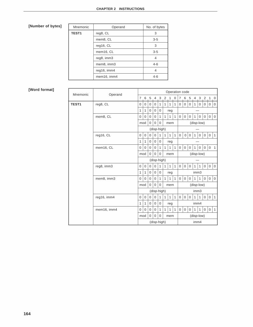
164
CHAPTER 2 INSTRUCTIONS
[Number of bytes]
[Word format]Mnemonic Operand
Operation code
7 6 5 4 3 2 1 0 7 6 5 4 3 2 1 0
TEST1 reg8, CL 0 0 0 0 1 1 1 1 0 0 0 1 0 0 0 0
1 1 0 0 0 reg —
mem8, CL 0 0 0 0 1 1 1 1 0 0 0 1 0 0 0 0
mod 0 0 0 mem (disp-low)
(disp-high) —
reg16, CL 0 0 0 0 1 1 1 1 0 0 0 1 0 0 0 1
1 1 0 0 0 reg —
mem16, CL 0 0 0 0 1 1 1 1 0 0 0 1 0 0 0 1
mod 0 0 0 mem (disp-low)
(disp-high) —
reg8, imm3 0 0 0 0 1 1 1 1 0 0 0 1 1 0 0 0
1 1 0 0 0 reg imm3
mem8, imm3 0 0 0 0 1 1 1 1 0 0 0 1 1 0 0 0
mod 0 0 0 mem (disp-low)
(disp-high) imm3
reg16, imm4 0 0 0 0 1 1 1 1 0 0 0 1 1 0 0 1
1 1 0 0 0 reg imm4
mem16, imm4 0 0 0 0 1 1 1 1 0 0 0 1 1 0 0 1
mod 0 0 0 mem (disp-low)
(disp-high) imm4
Mnemonic Operand No. of bytes
TEST1 reg8, CL 3
mem8, CL 3-5
reg16, CL 3
mem16, CL 3-5
reg8, imm3 4
mem8, imm3 4-6
reg16, imm4 4
mem16, imm4 4-6
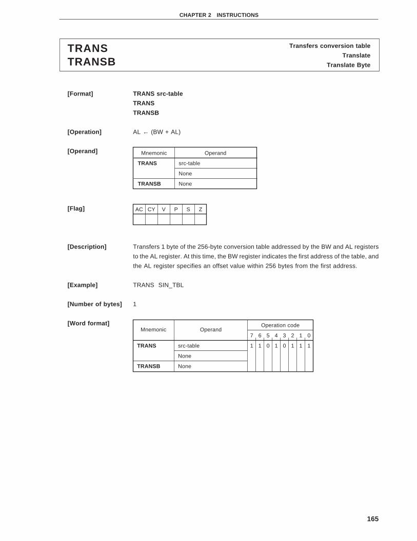
165
CHAPTER 2 INSTRUCTIONS
Transfers conversion tableTRANSTranslate
TRANSB Translate Byte
[Format] TRANS src-table
TRANS
TRANSB
[Operation] AL ← (BW + AL)
[Operand]
[Flag]
[Description] Transfers 1 byte of the 256-byte conversion table addressed by the BW and AL registers
to the AL register. At this time, the BW register indicates the first address of the table, and
the AL register specifies an offset value within 256 bytes from the first address.
[Example] TRANS SIN_TBL
[Number of bytes] 1
[Word format]
Mnemonic Operand
TRANS src-table
None
TRANSB None
AC CY V P S Z
Mnemonic OperandOperation code
7 6 5 4 3 2 1 0
TRANS src-table 1 1 0 1 0 1 1 1
None
TRANSB None

166
CHAPTER 2 INSTRUCTIONS
Exchanges dataXCHExchange
[Format] XCH dst, src
[Operation] dst ↔ src
[Operand]
[Flag]
[Description] Exchanges the contents of the destination operand (dst) specified by the first operand with
those of the source operand (src) specified by the second operand.
[Example] MOV AW, 100H
MOV BW, 50H
XCH AW, BW
; AW = 50H, BW = 100H
[Number of bytes]
[Word format]
Remark The operation code of the XCH AW, AW is the same as that of the NOP instruction.
Mnemonic Operand (dst, src)
XCH reg, reg’
mem, reg
reg, mem
AW, reg16
reg16, AW
AC CY V P S Z
Mnemonic Operand No. of bytes
XCH reg, reg’ 2
mem, reg 2-4
reg, mem
AW, reg16 1
reg16, AW
Mnemonic OperandOperation code
7 6 5 4 3 2 1 0 7 6 5 4 3 2 1 0
XCH reg, reg’ 1 0 0 0 0 1 1 W 1 1 reg reg’
mem, reg 1 0 0 0 0 1 1 W mod reg mem
(disp-low) (disp-high)
reg, mem 1 0 0 0 0 1 1 W mod reg mem
(disp-low) (disp-high)
AW, reg16 1 0 0 1 0 reg —
reg16, AW 1 0 0 1 0 reg —

167
CHAPTER 2 INSTRUCTIONS
Exclusive ORXORExclusive Or
[Format] XOR dst, src
[Operand, operation]
[Flag]
[Description] Exclusive-ORs the destination operand (dst) specified by the first operand with the source
operand (src) specified by the second operand, and stores the result to the destination
operand (dst).
[Example] • XOR CL, DL
• XOR CW, CW; Clears CW register
• XOR AW, DW
[Number of bytes]
Mnemonic Operand (dst, src) Operation
XOR reg, reg’ dst ← dst ∨ src
mem, reg
reg, mem
reg, imm
mem, imm
acc, imm [When W = 0] AL ← AL ∨ imm8
[When W = 1] AW ← AW ∨ imm16
AC CY V P S Z
U 0 0 × × ×
Mnemonic Operand (dst, src) No. of bytes
XOR reg, reg’ 2
mem, reg 2-4
reg, mem 2-4
reg, imm 3, 4
mem, imm 3-6
acc, imm 2, 3

168
CHAPTER 2 INSTRUCTIONS
[Word format]
Note The following code may be generated depending on the assembler or compiler used.
Even in this case, the instruction is executed normally. Note, however, that some emulators
do not support a function to disassemble or assemble this instruction.
Mnemonic OperandOperation code
7 6 5 4 3 2 1 0 7 6 5 4 3 2 1 0
XOR reg, reg’ 0 0 1 1 0 0 1 W 1 1 reg reg‘
mem, reg 0 0 1 1 0 0 0 W mod reg mem
(disp-low) (disp-high)
reg, mem 0 0 1 1 0 0 1 W mod reg mem
(disp-low) (disp-high)
reg, immNote 1 0 0 0 0 0 0 W 1 1 1 1 0 reg
imm8 or imm16-low imm16-high
mem, imm 1 0 0 0 0 0 0 W mod 1 1 0 mem
(disp-low) (disp-high)
imm8 or imm16-low imm16-high
acc, imm 0 0 1 1 0 1 0 W imm8 or imm16-low
imm16-high —
7 6 5 4 3 2 1 0 7 6 5 4 3 2 1 0
1 0 0 0 0 0 1 W 1 1 1 1 0 reg
imm8 —
169
CHAPTER 2 INSTRUCTIONS
2.2 Number of Instruction Execution Clocks
Table 2-8 shows the number of execution clocks of and the number of times word transfer is executed by each
instruction in the alphabetical order of the mnemonics.
(1) Clocks
The value indicated in the table is the time required for the execution unit to execute a given instruction and
is based on the following condition.
(a) This time does not include prefetch time, pre-decode time, and bus wait time.
(b) It is assumed that the number of wait cycles for memory access is 0.
Therefore, the number of clocks in one bus cycle is as follows:
• Other than V33A and V53A : 4 clocks
• V33A and V53A : 2 clocks
(c) It is assumed that the number of wait cycles for I/O access is 0.
(d) The primitive block transfer and primitive I/O instructions include the repeat prefix.
(e) When an odd address is accessed in word units, two bus cycles are started. The number of clocks required
for accessing an odd or even address is separately shown in the table.
(f) The external data bus width is as follows:
• V20, V20HL, V40, V40HL : 8 bits
• V30, V30HL, V50, V50HL, V33ANote , V53ANote : 16 bits
Note If the bus width is set to 16 bits by using the bus sizing function. To set the bus width to 8 bits,
increase the bus cycle to access word data in an even address by two-fold.
(g) The number of clocks of the V33A and V53A are shown in the normal address mode.
(2) Word transfers
“Word transfers” in the table indicates the number of words transferred, i.e., the number of times the word
data (16 bits) generated as a result of executing a given instruction is accessed on the bus.
By using this value, the number of instruction execution clocks when a wait state is inserted can be calculated
as follows:
• When an even address is accessed : (Number of instruction execution clocks with 0 wait)
+ (Number of times of word transfer) × (Number of wait statuses)
• When an odd address is accessed : (Number of instruction execution clocks with 0 wait)
+ (Number of times of word transfer) × (Number of wait statuses) × 2
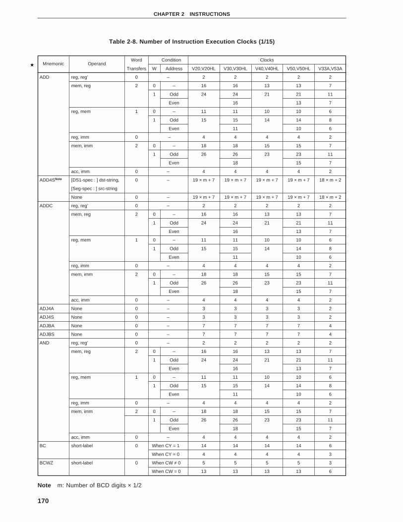
170
CHAPTER 2 INSTRUCTIONS
Table 2-8. Number of Instruction Execution Clocks (1/15)
Mnemonic OperandWord Condition Clocks
Transfers W Address V20,V20HL V30,V30HL V40,V40HL V50,V50HL V33A,V53A
ADD reg, reg’ 0 – 2 2 2 2 2
mem, reg 2 0 – 16 16 13 13 7
1 Odd 24 24 21 21 11
Even 16 13 7
reg, mem 1 0 – 11 11 10 10 6
1 Odd 15 15 14 14 8
Even 11 10 6
reg, imm 0 – 4 4 4 4 2
mem, imm 2 0 – 18 18 15 15 7
1 Odd 26 26 23 23 11
Even 18 15 7
acc, imm 0 – 4 4 4 4 2
ADD4SNote [DS1-spec : ] dst-string, 0 – 19 × m + 7 19 × m + 7 19 × m + 7 19 × m + 7 18 × m + 2
[Seg-spec : ] src-string
None 0 – 19 × m + 7 19 × m + 7 19 × m + 7 19 × m + 7 18 × m + 2
ADDC reg, reg’ 0 – 2 2 2 2 2
mem, reg 2 0 – 16 16 13 13 7
1 Odd 24 24 21 21 11
Even 16 13 7
reg, mem 1 0 – 11 11 10 10 6
1 Odd 15 15 14 14 8
Even 11 10 6
reg, imm 0 – 4 4 4 4 2
mem, imm 2 0 – 18 18 15 15 7
1 Odd 26 26 23 23 11
Even 18 15 7
acc, imm 0 – 4 4 4 4 2
ADJ4A None 0 – 3 3 3 3 2
ADJ4S None 0 – 3 3 3 3 2
ADJBA None 0 – 7 7 7 7 4
ADJBS None 0 – 7 7 7 7 4
AND reg, reg’ 0 – 2 2 2 2 2
mem, reg 2 0 – 16 16 13 13 7
1 Odd 24 24 21 21 11
Even 16 13 7
reg, mem 1 0 – 11 11 10 10 6
1 Odd 15 15 14 14 8
Even 11 10 6
reg, imm 0 – 4 4 4 4 2
mem, imm 2 0 – 18 18 15 15 7
1 Odd 26 26 23 23 11
Even 18 15 7
acc, imm 0 – 4 4 4 4 2
BC short-label 0 When CY = 1 14 14 14 14 6
When CY = 0 4 4 4 4 3
BCWZ short-label 0 When CW ≠ 0 5 5 5 5 3
When CW = 0 13 13 13 13 6
Note m: Number of BCD digits × 1/2

171
CHAPTER 2 INSTRUCTIONS
Table 2-8. Number of Instruction Execution Clocks (2/15)
Mnemonic OperandWord Condition Clocks
Transfers W Address V20,V20HL V30,V30HL V40,V40HL V50,V50HL V33A,V53A
BE short-label 0 When Z = 1 14 14 14 14 6
When Z = 0 4 4 4 4 3
BGE short-label 0 When S ∨ V = 1 4 4 4 4 3
When S ∨ V = 0 14 14 14 14 6
BGT short-label 0 When (S ∨ V) ∨ Z = 1 4 4 4 4 3
When (S ∨ V) ∨ Z = 0 14 14 14 14 6
BH short-label 0 When CY ∨ Z = 1 4 4 4 4 3
When CY ∨ Z = 0 14 14 14 14 6
BL short-label 0 When CY = 1 14 14 14 14 6
When CY = 0 4 4 4 4 3
BLE short-label 0 When (S ∨ V) ∨ Z = 1 14 14 14 14 6
When (S ∨ V) ∨ Z = 0 4 4 4 4 3
BLT short-label 0 When S ∨ V = 1 14 14 14 14 6
When S ∨ V = 0 4 4 4 4 3
BN short-label 0 When S = 1 14 14 14 14 6
When S = 0 4 4 4 4 3
BNC short-label 0 When CY = 1 4 4 4 4 3
When CY = 0 14 14 14 14 6
BNE short-label 0 When Z = 1 4 4 4 4 3
When Z = 0 14 14 14 14 6
BNH short-label 0 When CY ∨ Z = 1 14 14 14 14 6
When CY ∨ Z = 0 4 4 4 4 3
BNL short-label 0 When CY = 1 4 4 4 4 3
When CY = 0 14 14 14 14 6
BNV short-label 0 When V = 1 4 4 4 4 3
When V = 0 14 14 14 14 6
BNZ short-label 0 When Z = 1 4 4 4 4 3
When Z = 0 14 14 14 14 6
BP short-label 0 When S = 1 4 4 4 4 3
When S = 0 14 14 14 14 6
BPE short-label 0 When P = 1 14 14 14 14 6
When P = 0 4 4 4 4 3
BPO short-label 0 When P = 1 4 4 4 4 3
When P = 0 14 14 14 14 6
BR near-label 0 – 13 13 13 13 7
short-label 0 – 12 12 12 12 7
regptr16 0 – 11 11 11 11 7
memptr16 1 – Odd 24 24 23 23 13
Even 20 19 11
far-label 0 – 15 15 15 15 7
memptr32 2 – Odd 35 35 34 34 17
Even 27 26 13

172
CHAPTER 2 INSTRUCTIONS
Table 2-8. Number of Instruction Execution Clocks (3/15)
Mnemonic OperandWord Condition Clocks
Transfers W Address V20,V20HL V30,V30HL V40,V40HL V50,V50HL V33A,V53A
BRK 3 5 – Odd 50 50 50 50 24
Even 38 38 18
imm8 (≠3) 5 – Odd 50 50 50 50 24
Even 38 38 18
BRKEM imm8 5 – Odd 50 50 50 50 –
Even 38 38 –
BRKV None (when V = 1) 5 – Odd 52 52 52 52 26
Even 40 40 20
None (when V = 0) 5 – 3 3 3 3 3
BRKXA imm8 2 – – – – – 12
BUSLOCK None 0 – 2 2 2 2 2
BV short-label 0 When V = 1 14 14 14 14 6
When V = 0 4 4 4 4 3
BZ short-label 0 When Z = 1 14 14 14 14 6
When Z = 0 4 4 4 4 3
CALL near-proc 1 – Odd 20 20 20 20 9
Even 16 16 7
regptr16 1 – Odd 18 18 18 18 9
Even 14 14 7
memptr16 2 – Odd 31 31 31 31 15
Even 23 23 11
far-proc 2 – Odd 29 29 29 29 13
Even 21 21 9
memptr32 4 – Odd 47 47 47 47 23
Even 31 31 15
CALLN imm8 5 – Odd 58 58 58 58 –
Even 38 38 –
CHKIND reg16, mem32Note 7 – Odd 73-76 73-76 72-75 72-75 30-32(when interrupt condition
is satisfied) Even 53-56 52-55 24-26
reg16, mem32 2 – Odd 26 26 25 25 14(when interrupt condition
is not satisfied) Even 18 17 12
CLR1 reg8, CL 0 – 5 5 5 5 4
mem8, CL 0 – 14 14 11 11 9
reg16, CL 0 – 5 5 5 5 4
mem16, CL 2 – Odd 22 22 19 19 13
Even 14 11 9
reg8, imm3 0 – 6 6 6 6 4
mem8, imm3 0 – 15 15 12 12 9
reg16, imm4 0 – 6 6 6 6 4
mem16, imm4 2 – Odd 23 23 20 20 13
Even 15 12 9
CY 0 – 2 2 2 2 2
DIR 0 – 2 2 2 2 2
Note The number of clocks differs depending on the timing at which the interrupt is accepted.

173
CHAPTER 2 INSTRUCTIONS
Table 2-8. Number of Instruction Execution Clocks (4/15)
Mnemonic OperandWord Condition Clocks
Transfers W Address V20,V20HL V30,V30HL V40,V40HL V50,V50HL V33A,V53A
CMP reg, reg’ 0 – 2 2 2 2 2
mem, reg 1 0 – 11 11 10 10 6
1 Odd 15 15 14 14 8
Even 11 10 6
reg, mem 1 0 – 11 11 10 10 6
1 Odd 15 15 14 14 8
Even 11 10 6
reg, imm 0 – 4 4 4 4 2
mem, imm 1 0 – 13 13 12 12 6
1 Odd 17 17 16 16 8
Even 13 12 6
acc, imm 0 – 4 4 4 4 2
CMP4SNote 1 [DS1-spec : ] dst-string, 0 – 19 × m + 7 19 × m + 7 19 × m + 7 19 × m + 7 14 × m + 2
[Seg-spec : ] src-string
None 0 – 19 × m + 7 19 × m + 7 19 × m + 7 19 × m + 7 14 × m + 2
CMPBKNote 2 [Sg-spec : ] src-block, 2 × rep 0 – 7 + 14 × rep(13) 7 + 14 × rep(13) 7 + 14 × rep(13) 7 + 14 × rep(13) 12 × rep – 1(11)
[DS1-spec : ] dst-block (2) 1 Odd, odd 7 + 22 × rep(21) 7 + 22 × rep(21) 7 + 22 × rep(21) 7 + 22 × rep(21) 16 × rep – 1(15)
Odd, even 7 + 18 × rep(17) 7 + 18 × rep(17) 14 × rep – 1(13)
Even, even 7 + 14 × rep(13) 7 + 14 × rep(13) 12 × rep – 1(11)
CMPBKBNote 2 None 2 × rep (2) 0 – 7 + 14 × rep(13) 7 + 14 × rep(13) 7 + 14 × rep(13) 7 + 14 × rep(13) 12 × rep – 1(11)
CMPBKWNote 2 None 2 × rep 1 Odd, odd 7 + 22 × rep(21) 7 + 22 × rep(21) 7 + 22 × rep(21) 7 + 22 × rep(21) 16 × rep – 1(15)
(2) Odd, even 7 + 18 × rep(17) 7 + 18 × rep(17) 14 × rep – 1(13)
Even, even 7 + 14 × rep(13) 7 + 14 × rep(13) 12 × rep – 1(11)
CMPMNote 2 [DS1-spec : ] dst-block 1 × rep 0 – 7 + 10 × rep(7) 7 + 10 × rep(7) 7 + 10 × rep(7) 7 + 10 × rep(7) 10 × rep – 1(9)
(1) 1 Odd 7 + 14 × rep(11) 7 + 14 × rep(11) 7 + 14 × rep(11) 7 + 14 × rep(11) 12 × rep – 1(11)
Even 7 + 10 × rep(7) 7 + 10 × rep(7) 10 × rep – 1(9)
CMPMBNote 2 None 1 × rep 0 – 7 + 10 × rep(7) 7 + 10 × rep(7) 7 + 10 × rep(7) 7 + 10 × rep(7) 10 × rep – 1(9)
CMPMWNote 2 None 1 × rep 1 Odd 7 + 14 × rep(11) 7 + 14 × rep(11) 7 + 14 × rep(11) 7 + 14 × rep(11) 12 × rep – 1(11)
(1) Even 7 + 10 × rep(7) 7 + 10 × rep(7) 10 × rep – 1(9)
CVTBD None 0 – 15 15 15 15 12
CVTBW None 0 – 2 2 2 2 2
CVTDB None 0 – 7 7 7 7 8
CVTWLNote 3 None 0 – 4, 5 4, 5 4, 5 4, 5 2
DBNZ short-label 0 When CW ≠ 0 13 13 13 13 6
When CW = 0 5 5 5 5 3
DBNZE short-label 0 When CW ≠ 0 14 14 14 14 6
and Z = 1
Other than above 5 5 5 5 3
DBNZNE short-label 0 When CW ≠ 0 14 14 14 14 6
and Z = 0
Other than above 5 5 5 5 3
Notes 1. m: Number of BCD digits × 1/2
2. ( ): Applicable to processing that is performed only once
3. The number of clocks differs depending on the value of data (except the V33A and V53A).

174
CHAPTER 2 INSTRUCTIONS
Table 2-8. Number of Instruction Execution Clocks (5/15)
Mnemonic OperandWord Condition Clocks
Transfers W Address V20,V20HL V30,V30HL V40,V40HL V50,V50HL V33A,V53A
DEC reg8 0 – 2 2 2 2 2
mem 2 0 – 16 16 13 13 7
1 Odd 24 24 21 21 11
Even 16 13 7
reg16 0 – 2 2 2 2 2
DI None 0 – 2 2 2 2 2
DISPOSE None 1 – Odd 10 10 10 10 8
Even 6 6 6
DIVNote 1 reg8 0 – 29-34 29-34 29-34 29-34 17
mem8 0 – 34-39 34-39 34-39 34-39 20
reg16 0 – 38-43 38-43 38-43 38-43 24
mem16 1 – Odd 47-52 47-52 47-52 47-52 30
Even 43-48 43-48 28
DIVU reg8 0 – 19 19 19 19 11
mem8 0 – 25 25 24 24 15
reg16 0 – 25 25 25 25 19
mem16 1 – Odd 34 34 34 34 25
Even 30 30 23
DS0: None 0 – 2 2 2 2 2
DS1: None 0 – 2 2 2 2 2
EI None 0 – 2 2 2 2 2
EXTNote 2 reg8, reg8’ 1 or 2 – Odd 34-59 34-59 34-59 34-59 33-63
Even 26-55 26-55 29-61
reg8, imm4 1 or 2 – Odd 34-59 34-59 34-59 34-59 33-63
Even 26-55 26-55 29-61
FPO1 fp-op 0 – 2 2 2 2 Cannot be defined
fp-op, mem 1 – Odd 15 15 14 14 Cannot be defined
Even 11 10 Cannot be defined
FPO2 fp-op 0 – 2 2 2 2 Cannot be defined
fp-op, mem 1 – Odd 15 15 14 14 Cannot be defined
Even 11 10 Cannot be defined
HALT None 0 – 2 2 2 2 2
IN acc, imm8 1 0 – 9 9 9 9 5
1 Odd 13 13 13 13 7
EvenNote 3 9 9 5
acc,DW 1 0 – 8 8 8 8 5
1 Odd 12 12 12 12 7
EvenNote 3 8 8 5
INC reg8 0 – 2 2 2 2 2
mem 2 0 – 16 16 13 13 7
1 Odd 24 24 21 21 11
Even 16 13 7
reg16 0 – 2 2 2 2 2
Notes 1. The number of clocks differs depending on the value of data (except the V33A and V53A).
2. The number of clocks differs depending on the value of data.
3. The number of clocks of the V50, V50HL, and V53A is the same as the number of execution clocks of an
odd address because the bus cycle is started two times when the internal DMAU is accessed in word units.

175
CHAPTER 2 INSTRUCTIONS
Table 2-8. Number of Instruction Execution Clocks (6/15)
Mnemonic OperandWord Condition Clocks
Transfers W Address V20,V20HL V30,V30HL V40,V40HL V50,V50HL V33A,V53A
INMNote 1 [DS1-spec : ] dst-block, DW 2 × rep 0 – 9 + 8 × rep (10) 9 + 8 × rep (10) 9 + 8 × rep (10) 9 + 8 × rep (10) Note 3
(2) 1 Odd, odd 9 + 16 × rep (18) 9 + 16 × rep (18) 9 + 16 × rep (18) 9 + 16 × rep (18)
Odd, even 9 + 12 × rep (14) 9 + 12 × rep (14)
Even, even 9 + 8 × rep (10) 9 + 8 × rep (10)
INSNote 2 reg8, reg8’ 2 or 4 – Odd 35-133 35-133 35-133 35-133 39-77
Even 31-117 31-117 37-69
reg8, imm4 2 or 4 – Odd 35-133 35-133 35-133 35-133 39-77
Even 31-117 31-117 37-69
LDEA reg16, mem16 0 – 4 4 4 4 2
LDMNote 1 [Seg-spec : ] src-block 1 × rep 0 – 7 + 9 × rep (7) 7 + 9 × rep (7) 7 + 9 × rep (7) 7 + 9 × rep (7) 2 + 3 × rep (5)
(1) 1 Odd 7 + 13 × rep (11) 7 + 13 × rep (11) 7 + 13 × rep (11) 7 + 13 × rep (11) 2 + 5 × rep (7)
Even 7 + 9 × rep (7) 7 + 9 × rep (7) 2 + 3 × rep (5)
LDMBNote 1 None 1 × rep(1) 0 – 7 + 9 × rep (7) 7 + 9 × rep (7) 7 + 9 × rep (7) 7 + 9 × rep (7) 2 + 3 × rep (5)
LDMWNote 1 None 1 × rep 1 Odd 7 + 13 × rep (11) 7 + 13 × rep (11) 7 + 13 × rep (11) 7 + 13 × rep (11) 2 + 5 × rep (7)
(1) Even 7 + 9 × rep (7) 7 + 9 × rep (7) 2 + 3 × rep (5)
Notes 1. ( ): Applicable to processing that is performed only once
2. The number of clocks differs depending on the value of data.
3. The number of clocks of the V33A and V53A is as follows:
Mnemonic OperandWord Condition Clocks
Transfers W Address V33A V53A
INM [DS1-spec : ] dst-block, DW 2 × rep 0 – 4 + 8 × rep (12) 8 × rep (8)
(2) 1 Odd, odd 8 + 14 × rep (14) 14 × rep (14)
Odd, even If I/O address is odd: If I/O address is odd:
8 + 8 × rep (20) 12 × rep (12)
If memory address is odd: If memory address is odd:
4 + 10 × rep (14) 10 × rep (10)
Even, even 4 + 8 × rep (12) 8 × rep (8)

176
CHAPTER 2 INSTRUCTIONS
Table 2-8. Number of Instruction Execution Clocks (7/15)
Mnemonic OperandWord Condition Clocks
Transfers W Address V20,V20HL V30,V30HL V40,V40HL V50,V50HL V33A,V53A
MOV reg, reg’ 0 – 2 2 2 2 2
mem, reg 1 0 – 9 9 7 7 3
1 Odd 13 13 11 11 5
Even 9 7 3
reg, mem 1 0 – 11 11 10 10 5
1 Odd 15 15 14 14 7
Even 11 10 5
mem, imm 1 0 – 11 11 9 9 3
1 Odd 15 15 13 13 5
Even 11 9 3
reg, imm 0 – 4 4 4 4 2
acc, dmem 1 0 – 10 10 10 10 5
1 Odd 14 14 14 14 7
Even 10 10 5
dmem, acc 1 0 – 9 9 9 9 3
1 Odd 13 13 13 13 5
Even 9 9 3
sreg, reg16 0 – 2 2 2 2 2
sreg, mem16 1 – Odd 15 15 14 14 7
Even 11 10 5
reg16, sreg 0 – 2 2 2 2 2
mem16, sreg 1 – Odd 14 14 12 12 5
Even 10 8 3
DS0, reg16, mem32 2 – Odd 26 26 25 25 14
Even 18 17 10
DS1, reg16, mem32 2 – Odd 26 26 25 25 14
Even 18 17 10
AH, PSW 0 – 2 2 2 2 2
PSW, AH 0 – 3 3 3 3 2
MOVBKNote [DS1-spec : ] dst-block, 2 × rep 0 – 11 + 8 × rep (11) 11 + 8 × rep (11) 9 + 8 × rep (9) 9 + 8 × rep (9) 6 × rep (6)
[Seg-spec : ] src-block (2) 1 Odd, odd 11 + 16 × rep (19) 11 + 16 × rep (19) 9 + 16 × rep (17) 9 + 16 × rep (17) 10 × rep (10)
Odd, even 11 + 12 × rep (15) 9 + 12 × rep (13) 8 × rep (8)
Even, even 11 + 8 × rep (11) 9 + 8 × rep (9) 6 × rep (6)
MOVBKBNote None 2 × rep (2) 0 – 11 + 8 × rep (11) 11 + 8 × rep (11) 9 + 8 × rep (9) 9 + 8 × rep (9) 6 × rep (6)
MOVBKWNote None 2 × rep 1 Odd, odd 11 + 16 × rep (19) 11 + 16 × rep (19) 9 + 16 × rep (17) 9 + 16 × rep (17) 10 × rep (10)
(2) Odd, even 11 + 12 × rep (15) 9 + 12 × rep (13) 8 × rep (8)
Even, even 11 + 8 × rep (11) 9 + 8 × rep (9) 6 × rep (6)
Note ( ): Applicable to processing that is performed only once.

177
CHAPTER 2 INSTRUCTIONS
Table 2-8. Number of Instruction Execution Clocks (8/15)
Mnemonic OperandWord Condition Clocks
Transfers W Address V20,V20HL V30,V30HL V40,V40HL V50,V50HL V33A,V53A
MULNote reg8 0 – 33-39 33-39 33-39 33-39 8
mem8 0 – 39-45 39-45 38-44 38-44 12
reg16 0 – 41-47 41-47 41-47 41-47 12
mem16 1 – Odd 51-57 51-57 50-56 50-56 18
Even 47-53 46-52 16
reg16, imm8 0 – 28-34 28-34 28-34 28-34 12
reg16, imm16 0 – 36-42 36-42 36-42 36-42 12
reg16, reg16’, imm8 0 – 28-34 28-34 28-34 28-34 12
reg16, mem16, imm8 1 – Odd 38-44 38-44 37-43 37-43 18
Even 34-40 33-39 16
reg16, reg16’, imm16 0 – 36-42 36-42 36-42 36-42 12
reg16, mem16, imm16 1 – Odd 46-52 46-52 45-51 45-51 18
Even 42-48 41-47 16
MULUNote reg8 0 – 21, 22 21, 22 21, 22 21, 22 8
mem8 1 – 27, 28 27, 28 26, 27 26, 27 12
reg16 0 – 29, 30 29, 30 29, 30 29, 30 12
mem16 1 – Odd 39, 40 39, 40 38, 39 38, 39 18
Even 35, 36 34, 35 16
NEG reg 0 – 2 2 2 2 2
mem 2 0 – 16 16 13 13 7
1 Odd 24 24 21 21 11
Even 16 13 7
NOP None 0 – 3 3 3 3 3
NOT reg 0 – 2 2 2 2 2
mem 2 0 – 16 16 13 13 7
1 Odd 24 24 21 21 11
Even 16 13 7
NOT1 reg8, CL 0 – 4 4 4 4 4
mem8, CL 0 – 13 13 10 10 9
reg16, CL 0 – 4 4 4 4 4
mem16, CL 2 – Odd 21 21 18 18 13
Even 13 10 9
reg8, imm3 0 – 5 5 5 5 4
mem8, imm3 0 – 14 14 11 11 9
reg16, imm4 0 – 5 5 5 5 4
mem16, imm4 2 – Odd 22 22 19 19 13
Even 14 11 9
CY 0 – 2 2 2 2 2
Note The number of clocks differs depending on the value of data (except the V33A and V53A).
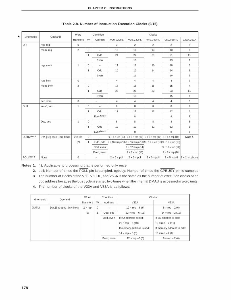
178
CHAPTER 2 INSTRUCTIONS
Table 2-8. Number of Instruction Execution Clocks (9/15)
Mnemonic OperandWord Condition Clocks
Transfers W Address V20,V20HL V30,V30HL V40,V40HL V50,V50HL V33A,V53A
OR reg, reg’ 0 – 2 2 2 2 2
mem, reg 2 0 – 16 16 13 13 7
1 Odd 24 24 21 21 11
Even 16 13 7
reg, mem 1 0 – 11 11 10 10 6
1 Odd 15 15 14 14 8
Even 11 10 6
reg, imm 0 – 4 4 4 4 2
mem, imm 2 0 – 18 18 15 15 7
1 Odd 26 26 23 23 11
Even 18 15 7
acc, imm 0 – 4 4 4 4 2
OUT imm8, acc 1 0 – 8 8 8 8 3
1 Odd 12 12 12 12 5
EvenNote 3 8 8 3
DW, acc 1 0 – 8 8 8 8 3
1 Odd 12 12 12 12 5
EvenNote 3 8 8 3
OUTMNote 1 DW, [Seg-spec : ] src-block 2 × rep 0 – 9 + 8 × rep (10) 9 + 8 × rep (10) 9 + 8 × rep (10) 9 + 8 × rep (10) Note 4
(2) 1 Odd, odd 9 + 16 × rep (18) 9 + 16 × rep (18) 9 + 16 × rep (18) 9 + 16 × rep (18)
Odd, even 9 + 12 × rep (14) 9 + 12 × rep (14)
Even, even 9 + 8 × rep (10) 9 + 8 × rep (10)
POLLNote 2 None 0 – 2 + 5 × poll 2 + 5 × poll 2 + 5 × poll 2 + 5 × poll 2 + 2 × cpbusy
Notes 1. ( ): Applicable to processing that is performed only once
2. poll: Number of times the POLL pin is sampled, cpbusy: Number of times the CPBUSY pin is sampled
3. The number of clocks of the V50, V50HL, and V53A is the same as the number of execution clocks of an
odd address because the bus cycle is started two times when the internal DMAU is accessed in word units.
4. The number of clocks of the V33A and V53A is as follows:
Mnemonic OperandWord Condition Clocks
Transfers W Address V33A V53A
OUTM DW, [Seg-spec : ] src-block 2 × rep 0 – 12 × rep – 6 (6) 8 × rep – 2 (6)
(2) 1 Odd, odd 22 × rep – 6 (16) 14 × rep – 2 (12)
Odd, even If I/O address is odd: If I/O address is odd:
20 × rep – 6 (10) 12 × rep – 2 (10)
If memory address is odd: If memory address is odd:
14 × rep – 6 (8) 10 × rep – 2 (8)
Even, even 12 × rep –6 (6) 8 × rep – 2 (6)

179
CHAPTER 2 INSTRUCTIONS
Table 2-8. Number of Instruction Execution Clocks (10/15)
Mnemonic OperandWord Condition Clocks
Transfers W Address V20,V20HL V30,V30HL V40,V40HL V50,V50HL V33A,V53A
POP mem16 2 – Odd 25 25 24 24 9
Even 17 16 5
reg16 1 – Odd 12 12 12 12 7
Even 8 8 5
sreg 1 – Odd 12 12 12 12 7
Even 8 8 5
PSW 1 – Odd 12 12 12 12 7
Even 8 8 5
R 7 – Odd 75 75 75 75 38
Even 43 43 22
PREPARE imm16, imm8 1 – Odd 16 16 16 16 15
(When imm8 = 0) Even 12 12
imm16, imm8 2 × imm8 – Odd 23 + 16 (imm8-1) 21 + 16 (imm8-1) 21 + 16 (imm8-1) 21 + 16 (imm8-1) 17 + 12 (imm8-1)
(When imm8 ≥ 1) Even 19 + 8 (imm8-1) 17 + 8 (imm8-1) 15 + 8 (imm8-1)
PS: None 0 – 2 2 2 2 2
PUSH mem16 2 – Odd 26 26 23 23 9
Even 18 15 5
reg16 1 – Odd 12 12 10 10 5
Even 8 6 3
sreg 1 – Odd 12 12 10 10 5
Even 8 6 3
PSW 1 – Odd 12 12 10 10 5
Even 8 6 3
R 8 – Odd 67 67 65 65 36
Even 35 33 20
imm8 1 – Odd 11 11 9 9 5
Even 7 5 3
imm16 1 – Odd 12 12 10 10 5
Even 8 6 3
REP None 0 – 2 2 2 2 2
REPC None 0 – 2 2 2 2 2
REPE None 0 – 2 2 2 2 2
REPNC None 0 – 2 2 2 2 2
REPNE None 0 – 2 2 2 2 2
REPNZ None 0 – 2 2 2 2 2
REPZ None 0 – 2 2 2 2 2
RET None 1 – Odd 19 19 19 19 12
(call in segment) Even 15 15 10
None 2 – Odd 29 29 29 29 16
(call outside segment) Even 21 21 12
pop-value 1 – Odd 24 24 24 24 12
(call in segment) Even 20 20 10
pop-value 2 – Odd 32 32 32 32 16
(call outside segment) Even 24 24 12
RETEM None 3 – Odd 39 39 39 39 –
Even 27 27 –

180
CHAPTER 2 INSTRUCTIONS
Table 2-8. Number of Instruction Execution Clocks (11/15)
Mnemonic OperandWord Condition Clocks
Transfers W Address V20,V20HL V30,V30HL V40,V40HL V50,V50HL V33A,V53A
RETI None 3 – Odd 39 39 39 39 19
Even 27 27 13
RETXA imm8 2 – – – – – 12
ROLNote reg, 1 0 – 6 6 6 6 2
mem, 1 2 0 – 16 16 13 13 7
1 Odd 24 24 21 21 11
Even 16 13 7
reg, CL 0 – 7 + n 7 + n 7 + n 7 + n 2 + n
mem, CL 2 0 – 19 + n 19 + n 16 + n 16 + n 6 + n
1 Odd 27 + n 27 + n 24 + n 24 + n 10 + n
Even 19 + n 16 + n 6 + n
reg, imm8 0 – 7 + n 7 + n 7 + n 7 + n 2 + n
mem, imm8 2 0 – 19 + n 19 + n 16 + n 16 + n 6 + n
1 Odd 27 + n 27 + n 24 + n 24 + n 10 + n
Even 19 + n 16 + n 6 + n
ROL4 reg8 0 – 13 13 13 13 9
mem8 0 – 28 28 25 25 15
ROLCNote reg, 1 0 – 6 6 6 6 2
mem, 1 2 0 – 16 16 13 13 7
1 Odd 24 24 21 21 11
Even 16 13 7
reg, CL 0 – 7 + n 7 + n 7 + n 7 + n 2 + n
mem, CL 2 0 – 19 + n 19 + n 16 + n 16 + n 6 + n
1 Odd 27 + n 27 + n 24 + n 24 + n 10 + n
Even 19 + n 16 + n 6 + n
reg, imm8 0 – 7 + n 7 + n 7 + n 7 + n 2 + n
mem, imm8 2 0 – 19 + n 19 + n 16 + n 16 + n 6 + n
1 Odd 27 + n 27 + n 24 + n 24 + n 10 + n
Even 19 + n 16 + n 6 + n
RORNote reg, 1 0 – 6 6 6 6 2
mem, 1 2 0 – 16 16 13 13 7
1 Odd 24 24 21 21 11
Even 16 13 7
reg, CL 0 – 7 + n 7 + n 7 + n 7 + n 2 + n
mem, CL 2 0 – 19 + n 19 + n 16 + n 16 + n 6 + n
1 Odd 27 + n 27 + n 24 + n 24 + n 10 + n
Even 19 + n 16 + n 6 + n
reg, imm8 0 – 7 + n 7 + n 7 + n 7 + n 2 + n
mem, imm8 2 0 – 19 + n 19 + n 16 + n 16 + n 6 + n
1 Odd 27 + n 27 + n 24 + n 24 + n 19 + n
Even 19 + n 16 + n 6 + n
ROR4 reg8 0 – 17 17 17 17 13
mem8 0 – 32 32 29 29 19
Note n: Number of times of shift

181
CHAPTER 2 INSTRUCTIONS
Table 2-8. Number of Instruction Execution Clocks (12/15)
Mnemonic OperandWord Condition Clocks
Transfers W Address V20,V20HL V30,V30HL V40,V40HL V50,V50HL V33A,V53A
RORCNote reg, 1 0 – 6 6 6 6 2
mem, 1 2 0 – 16 16 13 13 7
1 Odd 24 24 21 21 11
Even 16 13 7
reg, CL 0 – 7 + n 7 + n 7 + n 7 + n 2 + n
mem, CL 2 0 – 19 + n 19 + n 16 + n 16 + n 6 + n
1 Odd 27 + n 27 + n 24 + n 24 + n 10 + n
Even 19 + n 16 + n 6 + n
reg, imm8 0 – 7 + n 7 + n 7 + n 7 + n 2 + n
mem, imm8 2 0 – 19 + n 19 + n 16 + n 16 + n 6 + n
1 Odd 27 + n 27 + n 24 + n 24 + n 10 + n
Even 19 + n 16 + n 6 + n
SET1 reg8, CL 0 – 4 4 4 4 4
mem8, CL 0 – 13 13 10 10 9
reg16, CL 0 – 4 4 4 4 4
mem16, CL 2 – Odd 21 21 18 18 13
Even 13 10 9
reg8, imm3 0 – 5 5 5 5 4
mem8, imm3 0 – 14 14 11 11 9
reg16, imm4 0 – 5 5 5 5 4
mem16, imm4 2 – Odd 22 22 19 19 13
Even 14 11 9
CY 0 – 2 2 2 2 2
DIR 0 – 2 2 2 2 2
SHLNote reg, 1 0 – 6 6 6 6 2
mem, 1 2 0 – 16 16 13 13 7
1 Odd 24 24 21 21 11
Even 16 13 7
reg, CL 0 – 7 + n 7 + n 7 + n 7 + n 2 + n
mem, CL 2 0 – 19 + n 19 + n 16 + n 16 + n 6 + n
1 Odd 27 + n 27 + n 24 + n 24 + n 10 + n
Even 19 + n 16 + n 6 + n
reg, imm8 0 – 7 + n 7 + n 7 + n 7 + n 2 + n
mem, imm8 2 0 – 19 + n 19 + n 16 + n 16 + n 6 + n
1 Odd 27 + n 27 + n 24 + n 24 + n 10 + n
Even 19 + n 16 + n 6 + n
Note n: Number of times of shift

182
CHAPTER 2 INSTRUCTIONS
Table 2-8. Number of Instruction Execution Clocks (13/15)
Mnemonic OperandWord Condition Clocks
Transfers W Address V20,V20HL V30,V30HL V40,V40HL V50,V50HL V33A,V53A
SHRNote 1 reg, 1 0 – 6 6 6 6 2
mem, 1 2 0 – 16 16 13 13 7
1 Odd 24 24 21 21 11
Even 16 13 7
reg, CL 0 – 7 + n 7 + n 7 + n 7 + n 2 + n
mem, CL 2 0 – 19 + n 19 + n 16 + n 16 + n 6 + n
1 Odd 27 + n 27 + n 24 + n 24 + n 10 + n
Even 19 + n 16 + n 6 + n
reg, imm8 0 – 7 + n 7 + n 7 + n 7 + n 2 + n
mem, imm8 2 0 – 19 + n 19 + n 16 + n 16 + n 6 + n
1 Odd 27 + n 27 + n 24 + n 24 + n 10 + n
Even 19 + n 16 + n 6 + n
SHRANote 1 reg, 1 0 – 6 6 6 6 2
mem, 1 2 0 – 16 16 13 13 7
1 Odd 24 24 21 21 11
Even 16 13 7
reg, CL 0 – 7 + n 7 + n 7 + n 7 + n 2 + n
mem, CL 2 0 – 19 + n 19 + n 16 + n 16 + n 6 + n
1 Odd 27 + n 27 + n 24 + n 24 + n 10 + n
Even 19 + n 16 + n 6 + n
reg, imm8 0 – 7 + n 7 + n 7 + n 7 + n 2 + n
mem, imm8 2 0 – 19 + n 19 + n 16 + n 16 + n 6 + n
1 Odd 27 + n 27 + n 24 + n 24 + n 10 + n
Even 19 + n 16 + n 6 + n
SS: None 0 – 2 2 2 2 2
STMNote 2 [DS1-spec : ] dst-block 1 × rep 0 – 7 + 4 × rep (7) 7 + 4 × rep (7) 5 + 4 × rep (5) 5 + 4 × rep (5) 3 × rep (3)
(1) 1 Odd 7 + 8 × rep (11)7 + 8 × rep (11) 5 + 8 × rep (9) 5 + 8 × rep (9) 5 × rep (5)
Even 7 + 4 × rep (7) 5 + 4 × rep (5) 3 × rep (3)
STMBNote 2 None 1 × rep (2) 0 – 7 + 4 × rep (7) 7 + 4 × rep (7) 5 + 4 × rep (5) 5 + 4 × rep (5) 3 × rep (3)
STMWNote 2 None 1 × rep 1 Odd 7 + 8 × rep (11)7 + 8 × rep (11) 5 + 8 × rep (9) 5 + 8 × rep (9) 5 × rep (5)
(1) Even 7 + 4 × rep (7) 5 + 4 × rep (5) 3 × rep (3)
SUB reg, reg’ 0 – 2 2 2 2 2
mem, reg 2 0 – 16 16 13 13 7
1 Odd 24 24 21 21 11
Even 16 13 7
reg, mem 1 0 – 11 11 10 10 6
1 Odd 15 15 14 14 8
Even 11 10 6
reg, imm 0 – 4 4 4 4 2
mem, imm 2 0 – 18 18 15 15 7
1 Odd 26 26 23 23 11
Even 18 15 7
acc, imm 0 – 4 4 4 4 2
Notes 1. n: Number of times of shift
2. ( ): Applicable to processing that is performed only once

183
CHAPTER 2 INSTRUCTIONS
Table 2-8. Number of Instruction Execution Clocks (14/15)
Mnemonic OperandWord Condition Clocks
Transfers W Address V20,V20HL V30,V30HL V40,V40HL V50,V50HL V33A,V53A
SUB4SNote [DS1-spec : ] dst-string, 0 – 19 × m + 7 19 × m + 7 19 × m + 7 19 × m + 7 18 × m + 2
[Seg-spec : ] src-string
None 0 – 19 × m + 7 19 × m + 7 19 × m + 7 19 × m + 7 18 × m + 2
SUBC reg, reg’ 0 – 2 2 2 2 2
mem, reg 2 0 – 16 16 13 13 7
1 Odd 24 24 21 21 11
Even 16 13 7
reg, mem 1 0 – 11 11 10 10 6
1 Odd 15 15 14 14 8
Even 11 10 6
reg, imm 0 – 4 4 4 4 2
mem, imm 2 0 – 18 18 15 15 7
1 Odd 26 26 23 23 11
Even 18 15 7
acc, imm 0 – 4 4 4 4 2
TEST reg, reg’ 0 – 2 2 2 2 2
mem, reg 1 0 – 10 10 9 9 6
1 Odd 14 14 13 13 8
Even 10 9 6
reg, mem 1 0 – 10 10 9 9 6
1 Odd 14 14 13 13 8
Even 10 9 6
reg, imm 0 – 4 4 4 4 2
mem, imm 1 0 – 11 11 10 10 6
1 Odd 15 15 14 14 8
Even 11 10 6
acc, imm 0 – 4 4 4 4 2
TEST1 reg8, CL 0 – 3 3 3 3 4
mem8, CL 0 – 8 8 7 7 8
reg16, CL 0 – 3 3 3 3 4
mem16, CL 1 – Odd 12 12 11 11 10
Even 8 7 8
reg8, imm3 0 – 4 4 4 4 4
mem8, imm3 0 – 9 9 8 8 8
reg16, imm4 0 – 4 4 4 4 4
mem16, imm4 1 – Odd 13 13 12 12 10
Even 9 8 8
TRANS src-table 1 – 9 9 9 9 5
None 1 – 9 9 9 9 5
TRANSB None 1 – 9 9 9 9 5
Note m: Number of BCD digits × 1/2

184
CHAPTER 2 INSTRUCTIONS
Table 2-8. Number of Instruction Execution Clocks (15/15)
Mnemonic OperandWord Condition Clocks
Transfers W Address V20,V20HL V30,V30HL V40,V40HL V50,V50HL V33A,V53A
XCH reg, reg’ 0 – 3 3 3 3 3
mem, reg 2 0 – 16 16 13 13 8
1 Odd 24 24 21 21 12
Even 16 13 8
reg, mem 2 0 – 16 16 13 13 8
1 Odd 24 24 21 21 12
Even 16 13 8
AW, reg16 0 – 3 3 3 3 3
reg16, AW 0 – 3 3 3 3 3
XOR reg, reg’ 0 – 2 2 2 2 2
mem, reg 2 0 – 16 16 13 13 7
1 Odd 24 24 21 21 11
Even 16 13 7
reg, mem 1 0 – 11 11 10 10 6
1 Odd 15 15 14 14 8
Even 11 10 6
reg, imm 0 – 4 4 4 4 2
mem, imm 2 0 – 18 18 15 15 7
1 Odd 26 26 23 23 11
Even 18 15 7
acc, imm 0 – 4 4 4 4 2

185
APPENDIX A REGISTER CONFIGURATION
A.1 General-Purpose Registers (AW, BW, CW, DW)
Four 16-bit general-purpose registers are provided. These registers can be used not only as 16-bit registers but
also as 8- bit registers (AH, AL, BH, BL, CH, CL, DH, and DL) with each register divided into the high-order and low-
order 8 bits.
Therefore, these registers are used as 8- or 16-bit registers with a variety of instructions such as transfer, arithmetic
operation, and logical operation instructions. Also each register is used as a default register to process specific
instructions as follows:
AW : Word multiplication/division, word input/output, data exchange
AL : Byte multiplication/division, byte input/output, BCD rotate, data exchange
AH : Byte multiplication/division
BW : Data exchange (table reference)
CW : Loop control branch, repeat prefix
CL : Shift instructions, rotate instructions, BCD operation
DW : Word multiplication/division, indirect addressing input/output
A.2 Segment Registers (PS, SS, DS0, DS1)
The 16-bit V series divides the memory space into 64K-byte logical segments and can manage four segments at
the same time (segment method). The first address of each segment is specified by the following segment registers:
• Program segment register (PS): Specifies base address of segment storing instructions
• Stack segment register (SS) : Specifies base address of segment performing stack operations
• Data segment 0 register (DS0) : Specifies base address of segment storing data
• Data segment 1 register (DS1) : Specifies base address of segment used by data transfer instruction as
transfer destination of data
A.3 Pointers (SP, BP)
A pointer consists of two 16-bit registers (stack pointer (SP) and base pointer (BP)). Each register is used as a
pointer that specifies a memory address and can also be referenced in instruction. When memory data is referenced,
however, it is used as an index register.
SP indicates the address in the stack segment that stores the latest data, and is used as a default register when
the stack is manipulated.
BP is used to restore data saved to the stack.
A.4 Program Counter (PC)
PC is a 16-bit binary counter that holds the offset information of the program memory address to be executed by
the execution unit (EXU).
The value of PC is automatically incremented (+1) each time the microprogram fetches an instruction byte from
the instruction queue.
When the branch, call, return, or break instruction is executed, a new location is loaded to PC. At this time, the
value of PC is the same as that of the prefetch pointer (PFP).

186
APPENDIX A REGISTER CONFIGURATION
A.5 Program Status Word (PSW)
PSW consists of six status flags and four control flags.
Status flags
• Overflow flag (V)
• Sign flag (S)
• Zero flag (Z)
• Auxiliary carry flag (AC)
• Parity flag (P)
• Carry flag (CY)
Control flags
• Mode flag (MD)Note
• Direction flag (DIR)
• Interrupt enable flag (IE)
• Break flag (BRK)
Note Except the V33A and V53A
The status flag is automatically set to 1 or reset to 0 according to the result (data value) of executing an instruction.
The CY flag is directly set, reset, or inverted by an instruction.
The control flag is set or reset by an instruction to control the operation of the CPU.
The IE and BRK flags are reset when interrupt service is started.
Only the MD flag is set to 1 by RESET input, and all the other flags are reset to 0.
PSW is manipulated in byte or word units by the following processing. If it is manipulated in byte units, only the
low-order 8 bits (including the status flags except the V flag) are manipulated.
Figure A-1. PSW Configuration
Note The V33A and V53A is not provided with the MD flag. Bit 15 of PSW is fixed to 1.
Bits 0 through 7 can be stored to or restored from AH by the MOV instruction.
All the bits of PSW are saved to the stack when an interrupt occurs or when the call instruction is executed, and
are restored from the stack by the return instruction (RETI or RETEM)Note . In addition, PSW can also be saved to
or restored from the stack by the PUSH PSW or POP PSW instructionNote.
Note The MD flag may be in the write-enabled or write-disabled status. In the write-disabled status, the MD flag
is not restored from the stack but retains the current status even if the RETI or POP PSW instruction is
executed. The MD flag is set in the write-disabled status by the reset operation and RETEM instruction,
and is enabled by the BRKEM instruction.
15 14 13 12 11 10 9 8 7 6 5 4 3 2 1 0
MD
1 1 1 VDIR
IE
BRK
S Z 0AC 0 P 1 C
Y
Note
187
APPENDIX A REGISTER CONFIGURATION
Each flag is placed in the following status when each instruction is executed.
(1) Carry flag (CY)
(a) Binary addition/subtraction
When a byte operation is executed, and if a carry or borrow occurs from bit 7 of the result of the operation,
the CY flag is set; otherwise, it is reset.
If a carry or borrow occurs from bit 15 of the result of executing a word operation, the CY flag is set;
otherwise, it is reset.
(b) Logical operation
The CY flag remains reset regardless of the result.
(c) Binary multiplication
If AH is 0 as a result of executing an unsigned byte operation, the CY flag is reset; otherwise it is set.
If AH sign-extends AL as a result of executing a signed byte operation, the CY flag is reset; otherwise,
it is set.
If DW is 0 as a result of executing an unsigned word operation, the CY flag is reset; otherwise, it is set.
If DW sign-extends AW as a result of executing signed word operation, the CY flag is reset; otherwise,
it is set.
When an 8-bit immediate operation is executed, and if the product is within 16 bits, the CY flag is reset;
if the product exceeds 16 bits, it is set.
(d) Binary division
Undefined
(e) Shift/rotate
If a shift or rotate operation including the CY flag is executed, and if the bit shifted to the CY flag is 1,
the CY flag is set; otherwise, it is reset.
(2) Parity flag (P)
(a) Binary addition/subtraction, logical operation, shift
If the number of bits that are 1 of the low-order 8 bits of the result of an operation is even, the parity flag
is set; if the number of bits that are 1 is odd, the P flag is reset.
If the result is all 0, the P flag is set.
(b) Binary multiplication/division
Undefined

188
APPENDIX A REGISTER CONFIGURATION
(3) Auxiliary carry flag (AC)
(a) Binary addition/subtraction
The AC flag is set if a carry from the low-order 4 bits to the high-order 4 bits or a borrow from the high-
order 4 bits to the low-order 4 bits occur as a result of a byte operation; otherwise, it is reset.
When a word operation is executed, the AC flag is set or reset according to the status of the low-order
byte.
(b) Logical operation, binary multiplication/division, shift/rotate
Undefined
(4) Zero flag (Z)
(a) Binary addition/subtraction, logical operation, shift/rotate
If all the 8 bits of the result of a byte operation are zero, or if all the 16 bits of the result of a word operation
are zero, the zero flag is set; otherwise, it is reset.
(b) Binary multiplication/division
Undefined
(5) Sign flag (S)
(a) Binary addition/subtraction, logical operation, shift/rotate
If bit 7 of the result of a byte operation is 1, the sign flag is set; otherwise, it is reset.
If bit 15 of the result of a word operation is 1, the sign flag is set; otherwise, it is reset.
(b) Binary multiplication/division
Undefined
(6) Overflow flag (V)
(a) Binary addition/subtraction
If carries from bits 7 and 6 are different as a result of a byte operation, the overflow flag is set; otherwise,
it is reset.
If carries from bits 15 and 14 are different as a result of a word operation, the V flag is set; otherwise it
is reset.
(b) Binary multiplication
If AH is 0 as a result of an unsigned byte operation, the V flag is set; if AH is other than 0, the flag is reset.
If AH sign-extends AL as a result of a signed byte operation, the V flag is reset; otherwise, it is reset.
If DW is 0 as a result of an unsigned word operation, the V flag is reset; if DW is other than 0, it is set.
If DW sign-extends AW as a result of a signed word operation, the V flag is reset; otherwise, it is set.
If the product resulting from an 8-bit immediate operation is within 16 bits, the V flag is reset; if the product
exceeds 16 bits, it is set.
(c) Binary division
The V flag is reset.

189
APPENDIX A REGISTER CONFIGURATION
(d) Logical operation
The V flag is reset.
(e) Shift/rotate
When a left 1-bit shift/rotate operation is executed, the V flag is set or reset as follows according to the
result of the operation.
CY = most significant bit: reset
CY ≠ most significant bit: set
When a right 1-bit shift/rotate operation is executed, the V flag is set or reset as follows according to the
result of the operation.
Most significant bit = second most significant bit: reset
Most significant bit ≠ second most significant bit: set
The V flag is undefined if a multi-bit shift/rotate operation is executed.
(7) Break flag (BRK)
This flag can be set by a memory manipulation instruction only when it is saved to the stack as a part of PSW.
After the BRK flag has been set and restored from the stack to PSW, setting the BRK flag is effective.
Once the BRK flag has been set, and when one instruction is executed, a software interrupt (interrupt vector
1) automatically occurs, and one instruction can be traced at a time.
(8) Interrupt enable flag (IE)
This flag is set by the EI instruction to enable the INT interrupt, and is reset by the DI instruction to disable
the INT interrupt.
(9) Direction flag (DIR)
This flag is set by the SET1 DIR instruction and is reset by the CLR1 DIR instruction.
When the DIR flag is set, and if a block transfer/input/output instruction is executed, the processing is
performed from the high-order address to the low-order address. If the DIR flag is reset, the processing is
performed from the low-order address to the high-order address.
(10) Mode flag (MD) (except V33A and V53A)
This flag is set by RESET input and sets the CPU in the native mode. It is reset by the BRKEM instruction
to set the CPU in the emulation mode.
The MD flag is also set by the CALLN and RETEM instructions to set the CPU in the native mode.
The RESET input and RETEM instruction disables the MD flag from being written. As a result, the MD flag
is not restored even if the RETI or POP PSW instruction is executed. The BRKEM instruction enables writing
the MD flag.

190
APPENDIX A REGISTER CONFIGURATION
A.6 Index Registers (IX, IY)
These two index registers are 16-bit registers. Each register can be referenced in an instruction, and is also used
as an index register to generate effective address when memory data is referenced. Moreover, each register has a
special role as follows when a specific instruction processing is performed.
IX : Source operand address register for block data manipulation instruction
Base register for variable-length bit field manipulation instruction
Source operand address register for BCD string operation instruction
IY : Destination operand address register for block data manipulation instruction
Base register for variable-length bit field manipulation instruction
Destination operand address register for BCD string operation instruction

191
APPENDIX B ADDRESSING MODES
B.1 Instruction Address
The instruction address is automatically incremented each time an instruction is executed. In addition, the
instruction execution sequence can be controlled in various ways, as follows:
(1) Direct addressing
In this addressing mode, 2- or 4-byte immediate data in the instruction byte is directly loaded to PC or PS or
both PC and PS, and is used as a branch address.
This addressing mode is used to execute the following instructions:
CALL far-proc
CALL memptr16
CALL memptr32
BR far-label
BR memptr16
BR memptr32
(2) Relative addressing
In this addressing mode, 1- or 2-byte immediate data in the instruction byte is added as a signed displacement
value to PC and is used as a branch address.
If an 8-bit displacement is used, it is sign-extended and is added to PC as 16-bit data.
When the displacement is added, the contents of PC indicate the first address of the following instructions,
and this addressing mode is used to execute the following instructions.
CALL near-proc
BR near-label
BR short-label
Conditional branch instruction short-label
(3) Register addressing
In this addressing mode, the contents of any 16-bit register specified by the 3-bit register specification field
in the instruction byte are loaded to PC as a branch address.
Unlike when data is used, all the eight 16-bit registers (AW, BW, CW, DW, IX, IY, SP, and BP) can be used.
This addressing mode is used to execute the following instructions:
Example
CALL regptr16 CALL AW
BR regptr16 BR BW

192
APPENDIX B ADDRESSING MODES
(4) Register indirect addressing
In this addressing mode, the contents (word or double word) of the memory addressed by a 16-bit register
(IX, IY, or BW) specified by the register specification field in the instruction byte are loaded to PC (or both
PC and PS) as a branch address.
Example
CALL memptr16 CALL WORD PTR [IX]
CALL memptr32 CALL DWORD PTR [IY]
BR memptr16 BR WORD PTR [BW]
BR memptr32 BR DWORD PTR [IX]
Remark The assembler generates the instruction code of memptr16 for the instruction for which WORD
PTR is specified, and the instruction code of memptr32 for the instruction for which DWORD PTR
is specified.
(5) Indexed addressing
In this addressing mode, the 1- or 2-byte immediate data in the instruction byte is added as a signed
displacement to a 16-bit index register (IX or IY), and the contents (word or double word) addressed by the
result of the addition are loaded to PC as a branch address.
This addressing mode is used to execute the following instructions.
Example
CALL memptr16 CALL var [IX] [2]
CALL memptr32 CALL var [IY]
BR memptr16 BR var [IY]
BR memptr32 BR var [IX+4]
Remark If variable var has a word attribute, the assembler generates the instruction code of memptr16.
If the variable has a double word attribute, the assembler generates the instruction code of
memptr32.
(6) Based addressing
In this addressing mode, the 1- or 2-byte immediate data in the instruction byte are added to a 16-bit base
register (BP or BW) as a signed displacement value, and the contents (word or double word) addressed by
the result of the addition are loaded to PC as a branch address.
This addressing mode is used to execute the following instructions.
Example
CALL memptr16 CALL var [BP+2]
CALL memptr32 CALL var [BP]
BR memptr16 BR var [BW] [2]
BR memptr32 BR var [BP]
Remark If variable var has a word attribute, the assembler generates the instruction code of memptr16.
If the variable has a double word attribute, the assembler generates the instruction code of
memptr32.

193
APPENDIX B ADDRESSING MODES
(7) Based indexed addressing
In this addressing mode, the 1- or 2-byte immediate data in the instruction byte as a signed displacement value,
the contents of a 16-bit base register (BP or BW), and the contents of a 16-bit index register (IX or IY) are
added, and the contents (word or double word) of memory addressed by the result of the addition are loaded
to PC as a branch address.
This addressing mode is used to execute the following instructions.
Example
CALL memptr16 CALL var [BP] [IX]
CALL memptr32 CALL var [BW+2] [IY]
BR memptr16 BR var [BW] [2] [IX]
BR memptr32 BR var [BP+4] [IY]
Remark If variable var has a word attribute, the assembler generates the instruction code of memptr16.
If the variable has a double word attribute, the assembler generates the instruction code of
memptr32.
B.2 Memory Operand Address
The following several modes are used to address registers and memory to be manipulated when an instruction
is executed.
(1) Register addressing
In this mode, the contents of the register specification field (reg = 3-bit field, sreg = 2-bit field) in the instruction
byte address the register to be manipulated.
reg specifies, in combination with 1 bit (W) that specifies a word or byte in the instruction byte, eight types
of word registers (AW, BW, CW, DW, BP, SP, IX, and IY) and eight types of byte registers (AL, AH, BL, BH,
CL, CH, DL, and DH).
sreg specifies four types of segment registers (PS, SS, DS0, and DS1).
In some cases, the operation code of an instruction specifies a specific register.
This addressing mode is used to execute the instructions having the following operand description format.
Format Description
reg AW, BW, CW, DW, SP, BP, IX, IY,
AL, AH, BL, BH, CL, CH, DL, DH
reg16 AW, BW, CW, DW, SP, BP, IX, IY
reg8 AL, AH, BL, BH, CL, CH, DL, DH
sreg PS, SS, DS0, DS1
acc AW, AL
Example
If the case of MOV reg, reg’
MOV BP, SP
MOV AL, CL

194
APPENDIX B ADDRESSING MODES
(2) Immediate addressing
In this addressing mode, the 1- or 2-byte immediate data in the instruction byte is manipulated as is.
This mode is used to execute the instruction having the following operand description format.
Format Description
imm 8-/16-bit immediate data
imm16 16-bit immediate data
imm8 8-bit immediate data
pop-value 16-bit immediate data
In the case of imm, the assembler judges the value of imm described as the operand or the attribute of another
operand described at the same time to identify whether the data is 8 or 16 bits long, to determine word/byte
specification bit W.
Example
In the case of MOV reg, imm
MOV AL, 5; Byte
In the case of MUL reg16, reg16, imm16
MUL AW, BW, 1000H
(3) Direct addressing
In this mode, the immediate data in the instruction byte addresses the memory to be manipulated.
This mode is used to execute the instruction having the following operand description format.
Format Description
mem 16-bit variable specifying 8- or 16-bit memory data
dmem 16-bit variable specifying 8- or 16-bit memory data
imm4 4-bit variable indicating bit length of bit field data
Example
In the case of MOV mem, imm
MOV WORD_VAR, 2000H
In the case of MOV acc, dmem
MOV AL, BYTE_VAR
(4) Register indirect addressing
A 16-bit register (IX, IY, or BW) specified by the memory specification field (mod, mem) in the instruction byte
addresses the memory to be manipulated.
This mode is used to execute the instruction having the following operand description format.
Format Description
mem [IX], [IY], [BW]
Example
In the case of SUB mem, reg
SUB [IX], [AW]

195
APPENDIX B ADDRESSING MODES
(5) Auto-increment/decrement addressing
This addressing mode is a type of the register indirect addressing mode. In this mode, the register or memory
to be manipulated is addressed by the contents of a default register, and then the contents of the default register
are automatically incremented/decremented (+1/–1 in the case of byte processing and +2/–2 in the case of
word processing).
By using this addressing mode, the address is automatically updated for the next byte/word operand
processing.
Whether the register is incremented or decremented is indicated by the direction flag (DIR). If DIR = 0, the
register is incremented; if it is 1, the register is decremented.
This addressing mode is applicable to all the following default registers and is used to execute the instruction
with the following operand description mode.
Format Default register
dst-block IY
src-block IX
This addressing mode is used in combination with a counter (CW) that counts the number of times a byte/
word operand is repeatedly processed to control block data processing.
(6) Indexed addressing
In this addressing mode, 1- or 2-byte immediate data in the instruction byte is added to a 16-bit index register
(IX or IY) as a signed displacement value, and the result of this addition is used to address the memory operand
to be manipulated.
This addressing mode is effective for accessing data of array type. The displacement specifies the start
address of the array, and the contents of the index register specifies an array at the nth position from the start
address.
This addressing mode is used to execute the instruction having the following operand description format.
Format Description
mem var [IX], var [IY]
mem16 var [IX], var [IY]
mem8 var [IX], var [IY]
Example
In the case of TEST mem, imm
TEST BYTE_VAR [IX], 7FH
TEST BYTE_VAR [IX+8], 7FH
TEST WORD_VAR [IX] [8], 7FFFH
Remark If variable var has a byte attribute, a byte operand is specified. If var has a word attribute, a word
operand is specified. The assembler generates an instruction code corresponding to each
operand.

196
APPENDIX B ADDRESSING MODES
(7) Based addressing
In this addressing mode, 1- or 2-byte immediate data in the instruction byte is added as a signed displacement
value to a 16- bit base register (BP or BW), and the result of the addition addresses the memory operand to
be manipulated.
This addressing mode is effective for accessing data of structure type that is located at several positions in
memory. The base register specifies the start address of each structure, and the displacement selects one
element in each structure.
This addressing mode is used to execute the instruction having the following description format.
Format Description
mem var [BP], var [BW]
mem16 var [BP], var [BW]
mem8 var [BP], var [BW]
Example
In the case of SHL mem, 1
SHL BYTE_VAR [BP], 1
SHL WORD_VAR [BP+2], 1
SHL BYTE_VAR [BP] [4], 1
Remark If variable var has a byte attribute, a byte operand is specified. If var has a word attribute, a word
operand is specified. The assembler generates an instruction code corresponding to each
operand.
(8) Based indexed addressing
In this addressing mode, 1- or 2-byte immediate data in the instruction byte as a signed displacement value,
the contents of a 16-bit base register (BP or BW), and the contents of a 16-bit index register (IX or IY) are
added, and the result of the addition addresses the memory operand to be manipulated.
Because one piece of data can be specified by changing the contents of both the base register and index
register, this addressing mode is very effective for accessing data of structure type including an array type.
The base register specifies the first address of each structure, the displacement value indicates an offset from
the first address of the structure to the first address of array data, and the index register indicates the nth
position of the array data.
This addressing mode is used to execute the instruction having the following operand description format.
Format Description
mem var [base register][index register]
mem16 var [base register][index register]
mem8 var [base register][index register]
Example
In the case of PUSH mem16
PUSH WORD_VAR [BP] [IX]
PUSH WORD_VAR [BP+2] [IX+6]
PUSH WORD_VAR [BP] [4] [IX] [8]
197
APPENDIX B ADDRESSING MODES
(9) Bit addressing
In this addressing mode, 3- or 4-bit immediate data in the instruction byte, or the low-order 3 or 4 bits of the
CL register specify 1 bit of the 8- or 16-bit register or memory to be manipulated.
If an instruction is executed in this addressing mode, a specific 1 bit of a register or memory can be tested
(judgment of 0 or 1), set, cleared, or inverted without your having to be aware of the contents of the other bits.
This means that byte or word data does not need to be prepared to manipulate only 1 bit, like when the AND
or OR instruction is used.
This addressing mode is used to execute the instruction having the following description format.
Format Description
imm4 Bit number of word operand
imm3 Bit number of byte operand
CL CL
Example
TEST1 reg8, CL
TEST1 AL, CL
NOT1 reg8, imm3
NOT1 CL, 5
CLR1 mem16, CL
CLR1 WORD_VAR [IX], CL
SET1 mem16, imm4
SET1 WORD_VAR [BP], 9

198
[MEMO]
199
APPENDIX C INSTRUCTION MAP
[Legend]
Low Order×0H
High Order
0×H ADD
b, f, rm
High-order nibble (Table C-1: high-order 4 bits of first byte, Tables C-3 and C-4: high-order 4 bits of second byte)
[Condition included in instruction code]
b : Executes byte operation
d : Uses direct addressing
f : Involves reading from registers in CPU
i : Uses immediate data
ia : Uses immediate data and writes data back to accumulator
id : Uses indirect addressing
l : Involves control between segments
m : Uses memory data
reg8 : Uses 8-bit register
rm : Has effective address field in second byte
s : Uses sign-extended 16-bit immediate data
sr : Uses segment register
t : Writes registers in CPU
v : Indirectly specifies port number
w : Executes word operation
For the symbols other than above, refer to Table 2-4 Legend of Description on Instruction Format and Operand .
– – – – – – – – – – –
Low-order nibble (Table C-1: low-order 4 bits of first byte,
Tables C-3 and C-4: low-order 4 bits of second byte)
Mnemonic
Condition included in instruction code (Refer to below.)

200
APPENDIX C INSTRUCTION MAP
– – – – – – – – – – – – – – – – – – – – – – – – – – – – – – – – – – – – – – – – – – – – – – – – – – – – – – – – – – – – – – – – – – – – – – – – – – – – – – – – – – – – – – – – – – – – – –
– – – – – – – – – – – – – – – – – – – – – – – – – – – – – – – – – – – – – – – – – – – – – – – – – – – – – – – – – – – – – – – – – – – – – – – – – – – – – – – – – – – – – – – – – – – – – –
– – – – – – – – – – – – – – – – – – – – – – – – – – – – – – – – – – – – – – – – – – – – – – – – – – – – – – – – – – – – – – – – – – – – – – – – – – – – – – – – – – – – – – – – – – – – – –
– – – – – – – – – – – – – – – – – – – – – – – – – – – – – – – – – – – – – – – – – – – – – – – – – – – – – – – – – – – – – – – – – – – – – – – – – – – – – – – – – – – – – – – – – – – – – –
– – – – – – – – – – – – – – – – – – – – – – – – – – – – – – – – – – – – – – – – – – – – – – – – – – – – – – – – – – – – – – – – – – – – – – – – – – – – – – – – – – – – – – –
– – – – – – – – – – – – – – – – – – – – – – – – – – – – – – – – – – – – – – – – – – – – – – – – – – – – – – – – – – – – – – – – – – – – – – – – – – – – – – – – – – – – – – –
Table C-1. Instruction Map (1/2)
(a) Native mode
Low Order
×0H ×1H ×2H ×3H ×4H ×5H ×6H ×7H ×8H ×9H ×AH ×BH ×CH ×DH ×EH ×FHHighOrder
0×H ADD ADD ADD ADD ADD ADD PUSH POP OR OR OR OR OR OR PUSH Group3
b, f, rm w, f, rm b, t, rm w, t, rm b, ia w, ia DS1 DS1 b, f, rm w, f, rm b, t, rm w, t, rm b, ia w, ia PS
1×H ADDC ADDC ADDC ADDC ADDC ADDC PUSH POP SUBC SUBC SUBC SUBC SUBC SUBC PUSH POP
b, f, rm w, f, rm b, t, rm w, t, rm b, ia w, ia SS SS b, f, rm w, f, rm b, t, rm w, t, rm b, ia w, ia DS0 DS0
2×H AND AND AND AND AND AND DS1: ADJ4A SUB SUB SUB SUB SUB SUB PS: ADJ4S
b, f, rm w, f, rm b, t, rm w, t, rm b, ia w, ia b, f, rm w, f, rm b, t, rm w, t, rm b, ia w, ia
3×H XOR XOR XOR XOR XOR XOR SS: ADJBA CMP CMP CMP CMP CMP CMP DS0: ADJBS
b, f, rm w, f, rm b, t, rm w, t, rm b, ia w, ia b, f, rm w, f, rm b, t, rm w, t, rm b, ia w, ia
4×H INC INC INC INC INC INC INC INC DEC DEC DEC DEC DEC DEC DEC DEC
AW CW DW BW SP BP IX IY AW CW DW BW SP BP IX IY
5×H PUSH PUSH PUSH PUSH PUSH PUSH PUSH PUSH POP POP POP POP POP POP POP POP
AW CW DW BW SP BP IX IY AW CW DW BW SP BP IX IY
6×H PUSH POP CHKIND Undefined REPNC REPC FPO2 FPO2 PUSH MUL PUSH MUL INM INM OUTM OUTM
R R 0 1 w, i w, i s, i s, i b w b w
7×H BV BNV BC BNC BE BNE BNH BH BN BP BPE BPO BLT BGE BLE BGT
BL BNL BZ BNZ
8×H Imm Imm Imm Imm TEST TEST XCH XCH MOV MOV MOV MOV MOV LDEA MOV POP
b, rm w, rm b, s, rm w, s, rm b, rm w, rm b, rm w, rm b, f, rm w, f, rm b, t, rm w, t, rm sr, f, rm sr, t, rm rm
9×H NOPNote XCH XCH XCH XCH XCH XCH XCH CVTBW CVTWL CALL POLL PUSH POP MOV MOV
CW DW BW SP BP IX IY l, d PSW PSW PSW, AH AH, PSW
A×H MOV MOV MOV MOV MOVBK MOVBK CMPBK CMPBK TEST TEST STM STM LDM LDM CMPM CMPM
MOVBKB MOVBKB CMPBKB CMPBKB STMB STMB LDMB LDMB CMPMB CMPMB
MOVBKW MOVBKW CMPBKW CMPBKW STMW STMW LDMW LDMW CMPMW CMPMW
AL, m AW, m m, AL m, AW b w b w b, ia w, ia b w b w b w
B×H MOV MOV MOV MOV MOV MOV MOV MOV MOV MOV MOV MOV MOV MOV MOV MOV
AL, i CL, i DL, I BL, I AH, i CH, i DH, i BH, i AW, i CW, i DW, i BW, i SP, i BP, i IX, i IY, i
C×H Shift Shift RET RET MOV MOV MOV MOV PREPARE DISPOSE RET RET BRK BRK BRKV RETI
b, i w, i (SP) DS1 DS0 b, i, rm w, i, rm 1, (SP) 1 3 1
D×H Shift Shift Shift Shift CVTBD CVTDB Undefined TRANS FPO1 FPO1 FPO1 FPO1 FPO1 FPO1 FPO1 FPO1
TRANSB
b w b, v w, v 0 1 2 3 4 5 6 7
E×H DBNZE DBNZE DBNZ BCWZ IN IN OUT OUT CALL BR BR BR IN IN OUT OUT
b w b w d d l, d si, d b, v w, v b, v w, v
F×H BUSLOCK Undefined REPNE REP HALT NOT1 Group1 Group1 CLR1 SET1 DI EI CLR1 SET1 Group2 Group2
REPNZ REPE
REPZ
CY b w CY CY DIR DIR b w
– – – – – – – – – – – – – – – – – – – – – – – – – – – – – – – – – – – – – – – – – – – – – – – – – – – – – – – – – – – – – – – – – – – – – – – – – – – – – – – – – – – – – – – – – – – – – –
– – – – – – – – – – – – – – – – – – – – – – – – – – – – – – – – – – – – – – – – – – – – – – – – – – – – – – – – – – – – – – – – – – – – – – – – – – – – – – – – – – – – – – – – – – – – – –
– – – – – – – – – – – – – – – – – – – – – – – – – – – – – – – – – – – – – – – – – – – – – – – – – – – – – – – – – – – – – – – – – – – – – – – – – – – – – – – – – – – – – – – – – – – – – –
– – – – – – – – – – – – – – – – – – – – – – – – – – – – – – – – – – – – – – – – – – – – – – – – – – – – – – – – – – – – – – – – – – – – – – – – – – – – – – – – – – – – – – – – – – – – – –
– – – – – – – – – – – – – – – – – – – – – – – – – – – – – – – – – – – – – – – – – – – – – – – – – – – – – – – – – – – – – – – – – – – – – – – – – – – – – – – – – – – – – – – – – – – – – –
– – – – – – – – – – – – – – – – – – – – – – – – – – – – – – – – – – – – – – – – – – – – – – – – – – – – – – – – – – – – – – – – – – – – – – – – – – – – – – – – – – – – – – – – – – – – – –
– – – – – – – – – – – – – – – – – – – – – – – – – – – – – – – – – – – – – – – – – – – – – – – – – – – – – – – – – – – – – – – – – – – – – – – – – – – – – – – – – – – – – – – –
– – – – – – – – – – – – – – – – – – – – – – – – – – – – – – – – – – – – – – – – – – – – – – – – – – – – – – – – – – – – – – – – – – – – – – – – – – – – – – – – – – – – – – – – – – – – – –
– – – – – – – – – – – – – – – – – – – – – – – – – – – – – – – – – – – – – – – – – – – – – – – – – – – – – – – – – – – – – – – – – – – – – – – – – – – – – – – – – – – – – – – – – – – – – –
– – – – – – – – – – – – – – – – – – – – – – – – – – – – – – – – – – – – – – – – – – – – – – – – – – – – – – – – – – – – – – – – – – – – – – – – – – – – – – – – – – – – – – – – – – – – – –
Note Same operation code as XCH AW, AW
Caution : The instruction in Groups 1 and 2, and Imm, and Shift are determined by bits 3 through 5of the second byte of the instruction code (refer to Table C-2).The instruction in Group3 is determined by the second byte of the instruction code (referto Table C-4).

201
APPENDIX C INSTRUCTION MAP
Low Order
×0H ×1H ×2H ×3H ×4H ×5H ×6H ×7H ×8H ×9H ×AH ×BH ×CH ×DH ×EH ×FHHighOrder
0×H NOP LXI STAX INX INR DCR MVI RCL Undefined DAD LDAX DCX INR DCR MVI RRC
B, nn (nn) B B B B, n B B B C C C, n
1×H Undefined LXI STAX INX INR DCR MVI RAL Undefined DAD LDAX DCX INR DCR MVI RAR
D, nn (nn) D D D D, n D D D E E E, n
2×H Undefined LXI SHLD INX INR DCR MVI DAA Undefined DAD LHLD DXC INR DCR MVI CMA
H, nn (nn) H H H H, n H (nn) H L L L, n
3×H Undefined LXI STA INX INR DCR MVI SCF Undefined DAD LDA DCX INR DCR MVI CMC
SP, nn (nn) SP M M M, m SP (nn) SP A A A, n
4×H MOV MOV MOV MOV MOV MOV MOV MOV MOV MOV MOV MOV MOV MOV MOV MOV
B, B B, C B, D B, E B, H B, L B, M B, A C, B C, C C, D C, E C, H C, L C, M C, A
5×H MOV MOV MOV MOV MOV MOV MOV MOV MOV MOV MOV MOV MOV MOV MOV MOV
D, B D, C D, D D, E D, H D, L D, M D, A E, B E, C E, D E, E E, H E, L E, M E, A
6×H MOV MOV MOV MOV MOV MOV MOV MOV MOV MOV MOV MOV MOV MOV MOV MOV
H, B H, C H, D H, E H, H H, L H, M H, A L, B L, C L, D L, E L, H L, L L, M L, A
7×H MOV MOV MOV MOV MOV MOV HLT MOV MOV MOV MOV MOV MOV MOV MOV MOV
M, B M, C M, D M, E M, H M, L M, A A, B A, C A, D A, E A, H A, L A, M A, A
8×H ADD ADD ADD ADD ADD ADD ADD ADD ADC ADC ADC ADC ADC ADC ADC ADC
B C D E H L M A B C D E H L M A
9×H SUB SUB SUB SUB SUB SUB SUB SUB SBB SBB SBB SBB SBB SBB SBB SBB
B C D E H L M A B C D E H L M A
A×H ANA ANA ANA ANA ANA ANA ANA ANA XRA XRA XRA XRA XRA XRA XRA XRA
B C D E H L M A B C D E H L M A
B×H ORA ORA ORA ORA ORA ORA ORA ORA CMP CMP CMP CMP CMP CMP CMP CMP
B C D E H L M A B C D E H L M A
C×H RNZ POP JNZ JMP CNZ PUSH ADI RST RZ RET JZ Undefined CZ CALL ACI RST
B nn nn nn B n 0 nn nn nn n I
D×H RNC POP JNC OUT CNC PUSH SBI RST RC Undefined JC IN CC Undefined SBI RST
D nn n nn D n 2 nn n nn n 3
E×H RPO POP JPO XTHL CPO PUSH ANI RST RPE PCHL JPE XCHG CPE Group0 XRI RST
H nn nn H n 4 nn nn n 5
F×H RP POP JP DI CP PUSH ORI RST RM SPHL JM EI CM Undefined CPI RST
PSW nn nn PSW n 6 nn nn n 7
– – – – – – – – – – – – – – – – – – – – – – – – – – – – – – – – – – – – – – – – – – – – – – - – – – – – – – – – – – – – – – – – – – – – – – – – – – – – – – – – – – – – – – – –
– – – – – – – – – – – – – – – – – – – – – – – – – – – – – – – – – – – – – – – – – – – – – – – – – – – – – – – – – – – – – – – – – – – – – – – – – – – – – – – – – –
– – – – – – – – – – – – – – – – – – – – – – – – – – – – – – – – – – – – – – – – – – – – – – – – – – – – – – – – – – – – – – – – – – – – – – – – – – – – – – – – – –
– – – – – – – – – – – – – – – – – – – – – – – – – – – – – – – – – – – – – – – – – – – – – – – – – – – – – – – – – – – – – – – – – – – – – – – – – – – – – – – – – –
– – – – – – – – – – – – – – – – – – – – – – – – – – – – – – – – – – – – – – – – – – – – – – – – – – – – – – – – – – – – – – – – – – – – – – – – – – – – – – – – – – – – – – – – – – – – – –
– – – – – – – – – – – – – – – – – – – – – – – – – – – – – – – – – – – – – – – – – – – – – – – – – – – – – – – – – – – – – – – – – – – – – – – – – – – – – – – – – – – – – – – – – – – – – –
– – – – – – – – – – – – – – – – – – – – – – – – – – – – – – – – – – – – – – – – – – – – – – – – – – – – – – – – – – – – – – – – – – – – – – – – – – – – – – – – – – – – – – – – – – – – – –
Table C-1. Instruction Map (2/2)
(b) Emulation mode Note
– – – – – – – – – – – – – – – – – – – – – – – – – – – – – – – – – – – – – – – – – – – – – – – – – – – – – – – – – – – – – – – – – – – – – – – – – – – – – – – – – – – – – – – – – – – – – –
– – – – – – – – – – – – – – – – – – – – – – – – – – – – – – – – – – – – – – – – – – – – – – – – – – – – – – – – – – – – – – – – – – – – – – – – – – – – – – – – – – – – – – – – – – – – – –
– – – – – – – – – – – – – – – – – – – – – – – – – – – – – – – – – – – – – – – – – – – – – – – – – – – – – – – – – – – – – – – – – – – – – – – – – – – – – – – – – – – – – – – – – – – – – –
– – – – – – – – – – – – – – – – – – – – – – – – – – – – – – – – – – – – – – – – – – – – – – – – – – – – – – – – – – – – – – – – – – – – – – – – – – – – – – – – – – – – – – – – – – – – – –
– – – – – – – – – – – – – – – – – – – – – – – – – – – – – – – – – – – – – – – – – – – – – – – – – – – – – – – – – – – – – – – – – – – – – – – – – – – – – – – – – – – – – – – – – – – – – –
– – – – – – – – – – – – – – – – – – – – – – – – – – – – – – – – – – – – – – – – – – – – – – – – – – – – – – – – – – – – – – – – – – – – – – – – – – – – – – – – – – – – – – – -
– – – – – – – – – – – – – – – – – – – – – – – – – – – – – – – – – – – – – – – – – – – – – – – – – – – – – – – – – – – – – – – – – – – – – – – – – – – – – – – – – – – – – – – –
– – – – – – – – – – – – – – – – – – – – – – – – – – – – – – – – – – – – – – – – – – – – – – – – – – – – – – – – – – – – – – – – – – – – – – – – – – – – – – – – – – – – – – – – – – – – – –
– – – – – – – – – – – – – – – – – – – – – – – – – – – – – – – – – – – – – – – – – – – – – – – – – – – – - – – – – – – – – – – – – – – – – – - – – – – – – – – – – – –
Caution : The instruction in Group0 is determined by the second byte of the instruction code (refer
to Table C-3).
Note Subject: other than V33A and V53A

202
APPENDIX C INSTRUCTION MAP
Table C-3. Group0 Codes Note
Low Order
×0H ×DH ×FHHighOrder
0×H
E×H CALLN
i
F×H RETEM
Note Subject: other than V33A and V53A
Remark The blank column indicates an
undefined code.
Table C-2. Group1, Group2, Imm, and Shift Codes
Note000 001 010 011 100 101 110 111
Imm ADD OR ADDC SUB AND SUB XOR CMP
Shift ROL ROR ROLC RORC SHL SHR Undefined SHRA
Group1 TEST Undefined NOT NEG MULU MUL DIVU DIV
rm rm rm rm rm rm rm
Group2 INC DEC CALL CALL BR BR PUSH Undefined
rm rm id l, id id l, id rm
Note Bits 5 through 3 of second byte
– – – – – – – – – – – – – – – – – – – – – – – – – – – – – – – – – – – – – – – – – – – – – – –
– – – – – – – – – – – – – – – – – – – – – – – – – – – – – – – – – – – – – – – – –
– – – – – – – – – – – – – – – – – – – – – – – – – – – – – – – – – – – – – – – – –
– – – – – – – – – – – – – – – – – – – – – – – – – – – – – – – – – – – – – – – – –
Table C-4. Group3 Codes
Low Order
×0H ×1H ×2H ×3H ×4H ×5H ×6H ×7H ×8H ×9H ×AH ×BH ×CH ×DH ×EH ×FHHighOrder
0×H
1×H TEST1 TEST1 CLR1 CLR1 SET1 SET1 NOT1 NOT1 TEST1 TEST1 CLR1 CLR1 SET1 SET1 NOT1 NOT1
b w b w b w b w i, b i, w i, b i, w i, b i, w i, b i, w
2×H ADD4S SUB4S CMP4S ROL4 ROR4
3×H INS EXT INS EXT
reg8 reg8 i i
E×H BRKXANote 1
i
F×H RETXANote 1 BRKEMNote 2
i i
– – – – – – – – – – – – – – – – – – – – – – – – – – – – – – – – – – – – – – – – – – – – – – – – – – – – – – – – – – – – – – – – – – – – – – – – – – – – – – – – – – – – – – – – – – – – – –
– – – – – –– – – – – – – – – – – –
– – – – – –
– – – – – –
– – – – – –
– – – – – –
– – – – – –
Notes 1. V33A and V53A only (undefined code for other than V33A and V53A)
2. Other than V33A and V53A (Undefined code for V33A and V53A)
Remark The blank column indicates an undefined code.
– – – – – –– – – – – – – – – – – – – – – – – –– – – – – –
– – – – – –

203
APPENDIX D CORRESPONDENCE OF MNEMONICS OF µPD8086 AND 8088
The instruction set of the 16-bit V series is upward-compatible with the µPD8086 and 8088.
Table D-1 shows register correspondence between the µPD8086/8088 and 16-bit V series, and Table D-2 shows
mnemonic correspondence.
Table D-1. Register Correspondence with µPD8086 and 8088
µPD8086, 8088 16-Bit V Series µPD8086, 8088 16-Bit V Series
AL AL AX AW
CL CL CX CW
DL DL DX DW
BL BL BX BW
AH AH SP SP
CH CH BP BP
DH DH SI IX
BH BH DI IY

204
Table D-2. Mnemonic Correspondence with µPD8086 and 8088
µPD8086, 8088 16-Bit V Series
AAA ADJBA
AAD CVTDB
AAM CVTBD
AAS ADJBS
ADC ADDC
ADD ADD
AND AND
CALL CALL
CBW CVTBW
CLC CLR1 CY
CLD CLR1 DIR
CLI DI
CMC NOT1 CY
CMP CMP
CMPS CMPBK/
CMPBKB/
CMPBKW
CS: PS:
CWD CVTWL
DAA ADJ4A
DAS ADJ4S
DEC DEC
DIV DIVU
DS: DS0:
ES: DS1:
ESC FPO1
HLT HALT
IDIV DIV
IMUL MUL
IN IN
INC INC
INT BRK
INT 3 BRK 3
INTO BRKV
IRET RETI
JA BH
JAE BNC/BNL
µPD8086, 8088 16-Bit V Series
JB BC/BL
JBE BNH
JC BC/BL
JCXZ BCWZ
JE BE/BZ
JG BGT
JGE BGE
JL BLT
JLE BLE
JMP BR
JNA BNH
JNAE BC/BL
JNB BNC/BNL
JNBE BH
JNC BNC/BNL
JNE BNE/BNZ
JNG BLE
JNGE BLT
JNL BGE
JNLE BGT
JNO BNV
JNP BPO
JNS BP
JNZ BNE/BNZ
JO BV
JP BPE
JPE BPE
JPO BPO
JS BN
JZ BE/BZ
LAHF MOV AH, PSW
LDS MOV DS0
LEA LDEA
LES MOV DS1,
LOCK BUSLOCK
LODS LDM/LDMB/
LDMW
µPD8086, 8088 16-Bit V Series
LOOP DBNZ
LOOPE DBNZE
LOOPNE DBNZNE
LOOPNZ DBNZNE
LOOPZ DBNZE
MOV MOV
MOVS MOVBK
MOVSB MOVBKB
MOVSW MOVBKW
MUL MULU
NEG NEG
NOP NOP
NOT NOT
OR OR
OUT OUT
POP POP
POPF POP PSW
PUSH PUSH
PUSHF PUSH PSW
RCL ROLC
RCR RORC
REP REP
REPE REPE
REPNE REPNE
REPNZ REPNZ
REPZ REPZ
RET RET
ROL ROL
ROR ROR
SAHF MOV PSW, AH
SAL SHL
SAR SHRA
SBB SUBC
SCAS CMPM/
CMPMB/
CMPMW
SHL SHL
µPD8086, 8088 16-Bit V Series
SHR SHR
SS: SS:
STC SET1 CY
STD SET1 DIR
STI EI
STOS STM/STMB/
STMW
SUB SUB
TEST TEST
WAIT POLL
XCHG XCH
XLAT TRANS
XLATB TRANSB
XOR XOR
– ADD4S
– BRKEM
– BEKXA
– CALLN
– CHKIND
– CMP4S
– DISPOSE
– EXT
– FPO2
– INM
– INS
– OUTM
– PREPARE
– REPC
– REPNC
– RETEM
– RETXA
– ROL4
– ROR4
– SUB4S
– TEST1
Remark –: No corresponding instruction
APPENDIX D CORRESPONDENCE OF MNEMONICS OF µPD8086 AND 8088

205
APPENDIX E INSTRUCTION INDEX (mnemonic: by function)
[Data transfer]
LDEA ... 94
MOV ... 97
TRANS ... 165
TRANSB ... 165
XCH ... 166
[Repeat prefix]
REP ... 124
REPC ... 126
REPE ... 124
REPNC ... 127
REPNE ... 128
REPNZ ... 128
REPZ ... 124
[Primitive block transfer]
CMPBK ... 61
CMPBKB ... 61
CMPBKW ... 61
CMPM ... 63
CMPMB ... 63
CMPMW ... 63
LDM ... 95
LDMB ... 95
LDMW ... 95
MOVBK ... 100
MOVBKB ... 100
MOVBKW ... 100
STM ... 153
STMB ... 153
STMW ... 153
[Bit field manipulation]
EXT ... 81
INS ... 92
[Input/output]
IN ... 88
OUT ... 114
[Primitive input/output]
INM ... 90
OUTM ... 115
[Addition/subtraction]
ADD ... 13
ADDC ... 17
SUB ... 155
SUBC ... 159
[BCD operation]
ADD4S ... 15
CMP4S ... 59
ROL4 ... 136
ROR4 ... 141
SUB4S ... 157
[Increment/decrement]
DEC ... 72
INC ... 89
[Multiplication/division]
DIV ... 75
DIVU ... 77
MUL ... 102
MULU ... 105
[BCD adjustment]
ADJ4A ... 19
ADJ4S ... 20
ADJBA ... 21
ADJBS ... 22
[Data conversion]
CVTBD ... 65
CVTBW ... 66
CVTDB ... 67
CVTWL ... 68
[Compare]
CMP ... 57
[Complement operation]
NEG ... 107
NOT ... 109
206
[Logical operation]
AND ... 23
OR ... 112
TEST ... 161
XOR ... 167
[Bit manipulation]
CLR1 ... 54
NOT1 ... 110
SET1 ... 144
TEST1 ... 163
[Shift]
SHL ... 147
SHR ... 149
SHRA ... 151
[Rotate]
ROL ... 134
ROLC ... 137
ROR ... 139
RORC ... 142
[Subroutine control]
CALL ... 49
RET ... 129
[Stack manipulation]
DISPOSE ... 74
POP ... 118
PREPARE ... 120
PUSH ... 122
[Branch]
BR ... 41
[Conditional branch]
BC ... 25
BCWZ ... 26
BE ... 27
BGE ... 28
BGT ... 29
BH ... 30
BL ... 25
BLE ... 31
BLT ... 32
BN ... 33
BNC ... 34
BNE ... 35
BNH ... 36
BNL ... 34
BNV ... 37
BNZ ... 35
BP ... 38
BPE ... 39
BPO ... 40
BV ... 48
BZ ... 27
DBNZ ... 69
DBNZE ... 70
DBNZNE ... 71
[Interrupt]
BRK ... 43
BRKV ... 45
CHKIND ... 52
RETI ... 132
[CPU control]
BUSLOCK ... 47
DI ... 73
EI ... 80
FPO1 ... 83
FPO2 ... 85
HALT ... 87
NOP ... 109
POLL ... 117
[Segment override prefix]
DS0: ... 79
DS1: ... 79
PS: ... 79
SS: ... 79
[Emulation mode control]
BRKEM ... 44
CALLN ... 51
RETEM ... 131
[Extended address mode control]
BRKXA ... 46
RETXA ... 133
APPENDIX E INSTRUCTION INDEX (mnemonic: by function)

207
APPENDIX F INSTRUCTION INDEX (mnemonic: alphabetical order)
[A]
ADD ... 13
ADD4S ... 15
ADDC ... 17
ADJ4A ... 19
ADJ4S ... 20
ADJBA ... 21
ADJBS ... 22
AND ... 23
[B]
BC ... 25
BCWZ ... 26
BE ... 27
BGE ... 28
BGT ... 29
BH ... 30
BL ... 25
BLE ... 31
BLT ... 32
BN ... 33
BNC ... 34
BNE ... 35
BNH ... 36
BNL ... 34
BNV ... 37
BNZ ... 35
BP ... 38
BPE ... 39
BPO ... 40
BR ... 41
BRK ... 43
BRKEM ... 44
BRKV ... 45
BRKXA ... 46
BUSLOCK ... 47
BV ... 48
BZ ... 27
[C]
CALL ... 49
CALLN ... 51
CHKIND ... 52
CLR1 ... 54
CMP ... 57
CMP4S ... 59
CMPBK ... 61
CMPBKB ... 61
CMPBKW ... 61
CMPM ... 63
CMPMB ... 63
CMPMW ... 63
CVTBD ... 65
CVTBW ... 66
CVTDB ... 67
CVTWL ... 68
[D]
DBNZ ... 69
DBNZE ... 70
DBNZNE ... 71
DEC ... 72
DI ... 73
DISPOSE ... 74
DIV ... 75
DIVU ... 77
DS0: ... 79
DS1: ... 79
[E]
EI ... 80
EXT ... 81
[F]
FPO1 ... 83
FPO2 ... 85
[H]
HALT ... 87
[I]
IN ... 88
INC ... 89
INM ... 90
INS ... 92
[L]
LDEA ... 94
208
LDM ... 95
LDMB ... 95
LDMW ... 95
[M]
MOV ... 97
MOVBK ... 100
MOVBKB ... 100
MOVBKW ... 100
MUL ... 102
MULU ... 105
[N]
NEG ... 107
NOP ... 108
NOT ... 109
NOT1 ... 110
[O]
OR ... 112
OUT ... 114
OUTM ... 115
[P]
POLL ... 117
POP ... 118
PREPARE ... 120
PS: ... 79
PUSH ... 122
[R]
REP ... 124
REPC ... 126
REPE ... 124
REPNC ... 127
REPNE ... 128
REPNZ ... 128
REPZ ... 124
RET ... 129
RETEM ... 131
RETI ... 132
RETXA ... 133
ROL ... 134
ROL4 ... 136
ROLC ... 137
ROR ... 139
ROR4 ... 141
RORC ... 142
[S]
SET1 ... 144
SHL ... 147
SHR ... 149
SHRA ... 151
SS: ... 79
STM ... 153
STMB ... 153
STMW ... 153
SUB ... 155
SUB4S ... 157
SUBC ... 159
[T]
TEST ... 161
TEST1 ... 163
TRANS ... 165
TRANSB ... 165
[X]
XCH ... 166
XOR ... 167
APPENDIX F INSTRUCTION INDEX (mnemonic: alphabetical order)

Although NEC has taken all possible stepsto ensure that the documentation suppliedto our customers is complete, bug freeand up-to-date, we readily accept thaterrors may occur. Despite all the care andprecautions we've taken, you mayencounter problems in the documentation.Please complete this form wheneveryou'd like to report errors or suggestimprovements to us.
Hong Kong, Philippines, OceaniaNEC Electronics Hong Kong Ltd.Fax: +852-2886-9022/9044
KoreaNEC Electronics Hong Kong Ltd.Seoul BranchFax: 02-528-4411
TaiwanNEC Electronics Taiwan Ltd.Fax: 02-2719-5951
Address
North AmericaNEC Electronics Inc.Corporate Communications Dept.Fax: 1-800-729-9288
1-408-588-6130
EuropeNEC Electronics (Europe) GmbHTechnical Documentation Dept.Fax: +49-211-6503-274
South AmericaNEC do Brasil S.A.Fax: +55-11-6462-6829
Asian Nations except PhilippinesNEC Electronics Singapore Pte. Ltd.Fax: +65-250-3583
JapanNEC Semiconductor Technical HotlineFax: 044-435-9608
I would like to report the following error/make the following suggestion:
Document title:
Document number: Page number:
Thank you for your kind support.
If possible, please fax the referenced page or drawing.
Excellent Good Acceptable PoorDocument Rating
Clarity
Technical Accuracy
Organization
CS 00.6
Name
Company
From:
Tel. FAX
Facsimile Message