Embed Size (px)
Citation preview
140 JOURNAL OF MICROELECTROMECHANICAL SYSTEMS, VOL. 16, NO. 1, FEBRUARY 2007
An Electrostatic Zigzag Transmissive MicroopticalSwitch for MEMS Displays
Kerwin Wang, Michael Sinclair, Gary K. Starkweather, and Karl F. Böhringer, Senior Member, IEEE
Abstract—This paper presents the design and characterizationof the zigzag transmissive microoptical switch. It consists of ahighly space-efficient zigzag electrostatic actuator and opaqueshutter pair, which cover the optical channel in order to modulatea focused incident light beam. The novel zigzag design increasesthe electrostatic force and extends the stable travel range of theelectrostatic actuator. By adjusting the dimensions of the zigzag,it can operate both under digital and analog optical switching.The real-time shutter motions have been tested by a laser-inte-grated microscope. Experimental data demonstrate that a zigzagelectrostatic actuator of 47 �m � 160 �m size can achieve amaximum static lateral displacement of 10 �m (18 �m totalopening by a shutter pair) at 38 V. Depending on their design,zigzag devices have a mechanical resonance frequency of up to38.6 kHz with response time less than 20 �s and lifetime above7:6 � 109 cycles. [1661]
Index Terms—Electrostatic actuator, micro-optics, microopto-electromechanical system (MOEMS), optical switch, transmissiondisplay.
I. INTRODUCTION
TRANSMISSIVE microoptical switches (TMOS) haveplayed a critical role in optical telecommunication sys-
tems, optical network security systems, and also the JamesWebb space telescope [2]. In general, TMOS have a highlytunable optical output power range between on and off statesthat makes transmissive technology one of the most promisingcandidates to realize a high-contrast, self-illuminating pixeldisplay. In principle, a TMOS display can yield brighter andsharper images than most of the existing displays [3]–[12].However, TMOS display technology has remained underdevel-oped because it is difficult to design a free space, cost effective,sufficiently fast and power efficient actuator that fits into a
Manuscript received July 23, 2005; revised May 31, 2006. This work wassupported in part by a gift from Microsoft Research. The authors gratefullyacknowledge equipment and software donations from Agilent Technologies,Intel Corporation, Tanner Research, Inc. and Technic, Inc. The work of K. F.Böhringer was supported in part by an NSF CAREER award and by an Invita-tional Fellowship for Research in Japan from the Japan Society for the Promo-tion of Science (JSPS). This paper extends on a prior conference publication atthe 12th International Conference on Solid-State Sensors and Actuators (Trans-ducers’03) Boston, MA, June 6–12, 2003 [1]. Subject Editor O. Solgaard.
K. Wang and K. F. Böhringer are with the Department of Electrical En-gineering, University of Washington, Seattle, WA 98195-2500 USA (e-mail:[email protected]).
M. Sinclair and G. K. Starkweather are with Microsoft Research, Redmond,WA 98052 USA.
Color versions of one or more of the figures in this paper are available onlineat http://ieeexplore.ieee.org.
Digital Object Identifier 10.1109/JMEMS.2006.888913
self-illuminated display pixel (e.g., a 125- -squared area).Developing a novel actuator design to simultaneously achieveall these design goals under the various constraints imposedby material limits and process resolution of a commerciallyavailable MEMS process (e.g., MEMSCAP MUMPs) is evenmore challenging.
This paper introduces the zigzag electrostatic actuator forTMOS (see Fig. 1). The novel zigzag structure improves theforce-to-stiffness ratio of conventional electrostatic actuators.Because the actuators cannot share their working space with thelight path without blocking the light, the TMOS design incorpo-rates microlens arrays to form a complete display module thatimproves the optical efficiency and space coverage. Each mi-crolens focuses its portion of the light into a tunnel under the op-tical shutter; the shutter can modulate the light passing throughthe aperture depending on its opening dimensions. Another mi-crolens array behind the TMOS array projects the light onto adisplay screen or display module (see Fig. 2).
To initiate the TMOS design process for a practical display,we first discuss in Section II the design constraints given by thenaked human eye. The eye’s acuity and response informationcan be useful for determining TMOS size and speed. Then, wepresent an approach to determine the minimal size of the op-tical tunnel opening; it is constrained by the diffraction limitof light and by microlens properties. In Section III, we reviewstate-of-the-art electrostatic actuation technologies and intro-duce the zigzag actuator to achieve the design goals discussedin the previous section. We develop a flexibility model from thevirtual work principle for zigzag structures. This model is usedto estimate the fundamental resonance frequency of the zigzagstructure by Dunkerley’s method. We discuss the fringe effectin detail by comparing the electrostatic forces estimated withan analytic approach and with an electric field simulator. As aconsequence, a zigzag width-frequency design space is estab-lished. Fringing can be useful in actuator design to increase theelectrostatic force-to-stiffness ratio; practical implications aredemonstrated in physical devices. Then, in Section IV, we de-scribe a DRIE-based postprocess on the backside of a 1polysilicon MUMPs chip for the optical tunnel etching under-neath the shutters. The post-process ends with a PECVD hy-drophobic fluorocarbon polymer coating for good electrical iso-lation and low in-use stiction. In Section V, we present time-re-solved testing results. They show that depending on their geom-etry, zigzag actuators can be driven under both digital and analogswitching modes. Under analog mode, the shutter can have fullrange controllable motion without pull-in. All the design goalsare achieved.
1057-7157/$25.00 © 2007 IEEE

WANG et al.: AN ELECTROSTATIC ZIGZAG TRANSMISSIVE MICROOPTICAL SWITCH 141
Fig. 1. SEM micrographs of zigzag actuator pair (a) top view. (b) Perspective view.
II. DESIGN OF THE TRANSMISSIVE OPTICAL SWITCH
The TMOS consists of actuators, shutters and a miniaturizedoptical tunnel (see Fig. 2). Here we list the crucial design con-straints and goals for making a sequence of design decisions:
1) Determination of device size by checking the human eye’sacuity and resolution angle from a comfortable viewingdistance for proper image pixel size and resolution.
2) Checking the limitation of working frequency (switchingspeed) by examining the eye’s critical flicker frequency forstable imaging.
3) Determination of geometry of the optical tunnel and theshutter opening size by calculating the diffraction limit,depth of focus and numerical aperture (NA) with a coupledmicrolens for good transmissive light efficiency.
4) Creating a novel TMOS device by dual shutter and zigzagelectrostatic actuator design for high speed, space-efficient,low voltage transmissive micro-optical switching.
The first three decisions are briefly summarized below; theshutter and actuator design is discussed in detail in Section III.
A. TMOS Size and Resolution
For now let us assume that each TMOS represents one screenpixel on a single-color flat-panel display. The size of the phys-ical TMOS device should be equal to or less than the screenpixel size, which is limited by the comfortable viewing dis-tance due to the eye’s acuity. Most people can distinguish oneresolution angle feature
. For example, when looking at a computer monitor, thedistance between eyes and screen is around 45 cm. Then, theminimal distinguishable feature size for 1 arc minute is equal to
. Choosing the TMOS pitch (equalto microlens pitch and pixel size) of 125 satisfies this acuityconstraint and conforms to the resolution standards for displaysto obtain an HDTV quality image on an 11-inch or larger mon-itor.
B. Working Frequency
The main constraints on the working frequency of a TMOSare imposed by the display frame rate and a human eye’s crit-ical flicker frequency. Under analog mode, the TMOS shutteropening directly controls the brightness of a pixel. In this case,to see a stable image, the shutter speed should be greater than 60Hz for flicker-free operation. Alternately, under digital mode,control of pixel brightness is achieved by varying the duty cycle
Fig. 2. Cross-sectional view of an integrated TMOS display: From left to right,the collimated light is focused by a microlens array, passes through an opticaltunnel, is attenuated by the TMOS and projected to a display screen or a secondcollimating microlens array; upper right: conceptual perspective view of zigzagTMOS.
of the shutter. To control the pixel brightness at a rate of 60frames/s, an 8-bit, 256-level gray scale (monochrome) pixelshould be implemented by a TMOS at the working frequencyof 15.36 kHz . Thus, 15.36 kHz is chosen asthe design goal for our TMOS operation.
C. Optical Tunnel Design
An optical tunnel allows light focused by various microlenssystems to transmit through the substrate and reach the shutters(Fig. 2). From the aspects of actuator design and scaling effects,a small tunnel implies a small actuator size, small displacement,low driving voltage, low power consumption, and higher oper-ating frequencies. Thus, a small tunnel under the shutter is pre-ferred. However, the hole cannot shrink to zero size because ofthe limitations on diffraction spot size, numerical aperture, anddepth of focus (see Fig. 3).
1) Diffraction spot size [13], where iswavelength, is aperture, is the focal length and isthe focal number or focal ratio of the lens. Thus we obtainthe constraint , where is thelargest wavelength in use.

142 JOURNAL OF MICROELECTROMECHANICAL SYSTEMS, VOL. 16, NO. 1, FEBRUARY 2007
Fig. 3. Diffraction spot size DS, numerical aperture NA = D=(2f), anddepth of focus DOF > t in a TMOS, resulting in geometric constraints on theoptical tunnel width w and substrate thickness t.
2) Microlens numerical aperture , which is defined as. The diameter and depth of the tunnel
limits the selection of the numerical aperture of the lenssystem. Given the diameter of the cylindrical tunnel andthe substrate thickness (Fig. 3), the geometry of the op-tical path requires . Assumingand incorporating the diffraction spot size defined in thefirst limitation above, we get
.3) Depth of focus (DOF) is defined as the range from the
focal plane over which the working beam diameter varieswithin a specified limit. Depending on irradiance condi-tions and requirements, can be represented in dif-ferent formats [13]. In our case, when using a diffrac-tion-limited microlens system , thesubstrate thickness should be smaller than , thus
, otherwise a significantfraction of light would be blocked at the tunnel boundaries(see again Fig. 3). is the shortest wavelength in use.
Combining above constraints and choosing a diffraction-lim-ited lens system with (these values are com-monly available in microlens systems), and
for visible wavelengths, we obtain the fea-sible design space. Note that constraint 3 always dominates con-straint 2; however, when using a large range of wavelengths
, constraint 1 imposes a larger value on thanneeded for ; therefore, in practice we can relax constraint3 and only enforce constraint 2. For smaller f-number, aberra-tions have an adverse effect on both the spot size and depth offocus, whereas if the solution space is above f/8, aberrations arenegligible.
The design space in Fig. 4 shows that is theminimal allowed diameter for the optical tunnel. However, aconservative design strategy, using a larger cylindrical opening
and smaller substrate thickness , would avoid optical lossin the optical tunnel by tolerating misalignment or process-in-duced lens quality variation. A thinner substrate fits both lowand high lens systems; the major limitation on substratethickness is its mechanical strength. For example, if ,then is around 18.5 . Therefore, a 20- tunnel diam-eter is set up as a design goal, a substrate thickness of 150 ischosen for good optical transmission and mechanical strength.
Fig. 4. Design space of TMOS for visible light of wavelength � = 760 nm.The white region shows the feasible range for f=D and t. The region is boundedfrom below by minimum substrate thickness, from left and right by minimumand maximum focal number f=D, and from above by diffraction spot size DS(constraint 2) and depth of focus DOF (constraint 3).
TABLE IDESIGN PARAMETERS AND GOALS FOR THE TRANSMISSIVE OPTIC SWITCH
A shutter is sufficient to block the light emanatingfrom this spot. Misalignment between center of the shutters andthe tunnel should be controlled within submicron range. As asummary, all the critical dimensions are put together in Table I.
Because no existing microactuator could achieve all thesedesign goals, we have developed a novel electrostatic zigzagdesign. A brief review of electrostatic actuator designs is givenin the next section and corresponding state-of-the-art examplesare described before the zigzag electrostatic actuator drivenTMOS design is detailed and corresponding analytical studiesare given.
III. ELECTROSTATIC ZIGZAG ACTUATOR AND OPTICAL
SHUTTER DESIGN
Electrostatic microsensors and microactuators have beenwidely used in MEMS for more than two decades [14], [15]because of their low energy consumption, good scaling prop-erties to small dimensions and high energy densities. They canbe roughly classified into two categories, parallel-plate drivesand comb drives.
Parallel-plate drives have an electrostatic field inside the gapparallel to the electrode movement direction with a nonlinearrelationship between electrostatic force and displacement. The
WANG et al.: AN ELECTROSTATIC ZIGZAG TRANSMISSIVE MICROOPTICAL SWITCH 143
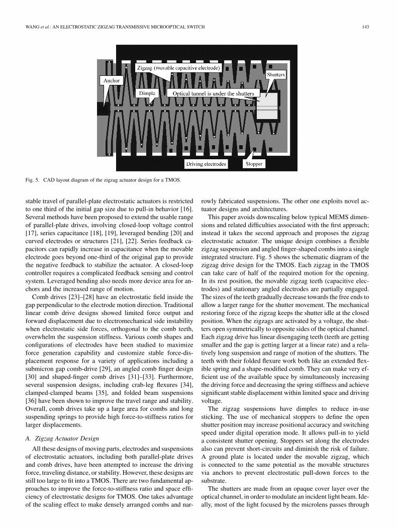
Fig. 5. CAD layout diagram of the zigzag actuator design for a TMOS.
stable travel of parallel-plate electrostatic actuators is restrictedto one third of the initial gap size due to pull-in behavior [16].Several methods have been proposed to extend the usable rangeof parallel-plate drives, involving closed-loop voltage control[17], series capacitance [18], [19], leveraged bending [20] andcurved electrodes or structures [21], [22]. Series feedback ca-pacitors can rapidly increase in capacitance when the movableelectrode goes beyond one-third of the original gap to providethe negative feedback to stabilize the actuator. A closed-loopcontroller requires a complicated feedback sensing and controlsystem. Leveraged bending also needs more device area for an-chors and the increased range of motion.
Comb drives [23]–[28] have an electrostatic field inside thegap perpendicular to the electrode motion direction. Traditionallinear comb drive designs showed limited force output andforward displacement due to electromechanical side instabilitywhen electrostatic side forces, orthogonal to the comb teeth,overwhelm the suspension stiffness. Various comb shapes andconfigurations of electrodes have been studied to maximizeforce generation capability and customize stable force-dis-placement response for a variety of applications including asubmicron gap comb-drive [29], an angled comb finger design[30] and shaped-finger comb drives [31]–[33]. Furthermore,several suspension designs, including crab-leg flexures [34],clamped-clamped beams [35], and folded beam suspensions[36] have been shown to improve the travel range and stability.Overall, comb drives take up a large area for combs and longsuspending springs to provide high force-to-stiffness ratios forlarger displacements.
A. Zigzag Actuator Design
All these designs of moving parts, electrodes and suspensionsof electrostatic actuators, including both parallel-plate drivesand comb drives, have been attempted to increase the drivingforce, traveling distance, or stability. However, these designs arestill too large to fit into a TMOS. There are two fundamental ap-proaches to improve the force-to-stiffness ratio and space effi-ciency of electrostatic designs for TMOS. One takes advantageof the scaling effect to make densely arranged combs and nar-
rowly fabricated suspensions. The other one exploits novel ac-tuator designs and architectures.
This paper avoids downscaling below typical MEMS dimen-sions and related difficulties associated with the first approach;instead it takes the second approach and proposes the zigzagelectrostatic actuator. The unique design combines a flexiblezigzag suspension and angled finger-shaped combs into a singleintegrated structure. Fig. 5 shows the schematic diagram of thezigzag drive design for the TMOS. Each zigzag in the TMOScan take care of half of the required motion for the opening.In its rest position, the movable zigzag teeth (capacitive elec-trodes) and stationary angled electrodes are partially engaged.The sizes of the teeth gradually decrease towards the free ends toallow a larger range for the shutter movement. The mechanicalrestoring force of the zigzag keeps the shutter idle at the closedposition. When the zigzags are activated by a voltage, the shut-ters open symmetrically to opposite sides of the optical channel.Each zigzag drive has linear disengaging teeth (teeth are gettingsmaller and the gap is getting larger at a linear rate) and a rela-tively long suspension and range of motion of the shutters. Theteeth with their folded flexure work both like an extended flex-ible spring and a shape-modified comb. They can make very ef-ficient use of the available space by simultaneously increasingthe driving force and decreasing the spring stiffness and achievesignificant stable displacement within limited space and drivingvoltage.
The zigzag suspensions have dimples to reduce in-usesticking. The use of mechanical stoppers to define the openshutter position may increase positional accuracy and switchingspeed under digital operation mode. It allows pull-in to yielda consistent shutter opening. Stoppers set along the electrodesalso can prevent short-circuits and diminish the risk of failure.A ground plate is located under the movable zigzag, whichis connected to the same potential as the movable structuresvia anchors to prevent electrostatic pull-down forces to thesubstrate.
The shutters are made from an opaque cover layer over theoptical channel, in order to modulate an incident light beam. Ide-ally, most of the light focused by the microlens passes through
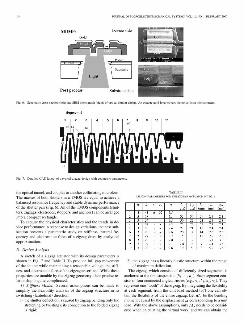
144 JOURNAL OF MICROELECTROMECHANICAL SYSTEMS, VOL. 16, NO. 1, FEBRUARY 2007
Fig. 6. Schematic cross section (left) and SEM micrograph (right) of optical shutter design. An opaque gold layer covers the polysilicon microshutters.
Fig. 7. Detailed CAD layout of a typical zigzag design with geometric parameters.
the optical tunnel, and couples to another collimating microlens.The masses of both shutters in a TMOS are equal to achieve abalanced resonance frequency and stable dynamic performanceof the shutter pair (Fig. 6). All of the TMOS components (shut-ters, zigzags, electrodes, stoppers, and anchors) can be arrangedinto a compact rectangle.
To capture the physical characteristics and the trends in de-vice performance in response to design variations, the next sub-section presents a parametric study on stiffness, natural fre-quency and electrostatic force of a zigzag drive by analyticalapproximation.
B. Design Analysis
A sketch of a zigzag actuator with its design parameters isshown in Fig. 7 and Table II. To produce full gap movementof the shutter while maintaining a reasonable voltage, the stiff-ness and electrostatic force of the zigzag are critical. While theseproperties are tunable by the zigzag geometry, their precise re-lationship is quite complicated.
1) Stiffness Model: Several assumptions can be made tosimplify the flexibility analysis of the zigzag structure in itsswitching (latitudinal) direction:
1) the shutter deflection is caused by zigzag bending only (nostretching or twisting); its connection to the folded zigzagis rigid;
TABLE IIDESIGN PARAMETERS FOR THE ZIGZAG ACTUATOR IN FIG. 7
2) the zigzag has a linearly elastic structure within the rangeof maximum deflection.
The zigzag, which consists of differently sized segments, isanchored at the first suspension ( , , ). Each segment con-sists of four connected angled trusses (e.g., , , , ). Theyrepresent one “tooth” of the zigzag. By integrating the flexibilityat each segment, from the unit load method [37] one can ob-tain the flexibility of the entire zigzag. Let be the bendingmoment caused by the displacement corresponding to a unitload. With the above assumptions, only needs to be consid-ered when calculating the virtual work, and we can obtain the

WANG et al.: AN ELECTROSTATIC ZIGZAG TRANSMISSIVE MICROOPTICAL SWITCH 145
general equation for displacement in response to a unit load inthe following form [37]:
(1)
represents the bending moment caused by the actual load.and represent the modulus of elasticity and area moment of
inertia, respectively. To find the flexibility of a given struc-ture, we replace the actual applied bending moment withthe unit bending moment in (1), and the flexibility of thezigzag structure can be represented as
(2)
, the flexibility, is measured in m/N. Based on (2) the flex-ibility of the zigzag structure in Fig. 7 can be integrated ac-cording to the following equation (3). Assuming the zigzag hasuniform width and moment of inertia everywhere, we find theflexibility at the right end of segment when a unit load isapplied
(3)
Fig. 8. Graph relating the stiffness of zigzag segments to their widths, calcu-lated with the unit load method.
Young’s modulus.
Area moment of inertia.
Flexibility at segment .
Effective length for calculating bendingmoment at the left edge of segmentwhen unit load is applied to the rightedge of segment ; e.g., and
.
, , , Length of beams , , , at segment , andthe corresponding beam skew angle.
, Beam width and thickness.
The local coordinate along each beamsegment.
Subscript refers to the segments , , , and of thezigzag in Fig. 7. The zigzag flexibility at the end of each segmentis a combination of the flexibility at the individual segment andthe flexibility of the entire suspension to its left.
A simple way to modify the flexibility is to adjust the width ofthe individual angled teeth. The parametric designs of zigzagsand electrodes have been described in Table II. A graph com-paring the stiffness of zigzag segments with a variety of widthsis shown in Fig. 8. The flexibility information at each segmentof the zigzag can help predict the fundamental resonance fre-quency of the zigzag.
2) Natural Frequency: By using the flexibility and mass in-formation of each zigzag segment and shutter, one can esti-mate the fundamental resonance frequency of the zigzag ac-tuator from Dunkerley’s method [38]. The method yields thefollowing expression to estimate a lower bound of fundamentalresonance frequency
(4)
146 JOURNAL OF MICROELECTROMECHANICAL SYSTEMS, VOL. 16, NO. 1, FEBRUARY 2007
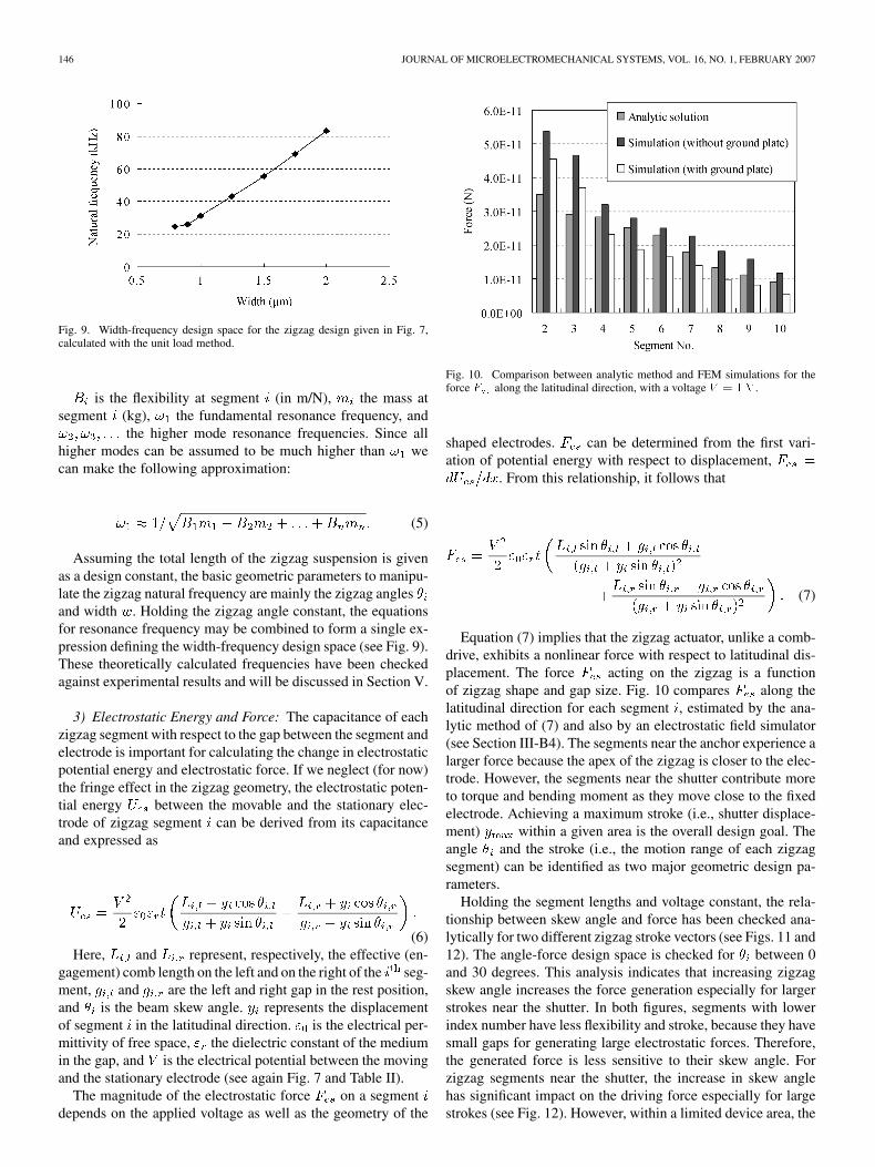
Fig. 9. Width-frequency design space for the zigzag design given in Fig. 7,calculated with the unit load method.
is the flexibility at segment (in m/N), the mass atsegment (kg), the fundamental resonance frequency, and
the higher mode resonance frequencies. Since allhigher modes can be assumed to be much higher than wecan make the following approximation:
(5)
Assuming the total length of the zigzag suspension is givenas a design constant, the basic geometric parameters to manipu-late the zigzag natural frequency are mainly the zigzag anglesand width . Holding the zigzag angle constant, the equationsfor resonance frequency may be combined to form a single ex-pression defining the width-frequency design space (see Fig. 9).These theoretically calculated frequencies have been checkedagainst experimental results and will be discussed in Section V.
3) Electrostatic Energy and Force: The capacitance of eachzigzag segment with respect to the gap between the segment andelectrode is important for calculating the change in electrostaticpotential energy and electrostatic force. If we neglect (for now)the fringe effect in the zigzag geometry, the electrostatic poten-tial energy between the movable and the stationary elec-trode of zigzag segment can be derived from its capacitanceand expressed as
(6)Here, and represent, respectively, the effective (en-
gagement) comb length on the left and on the right of the seg-ment, and are the left and right gap in the rest position,and is the beam skew angle. represents the displacementof segment in the latitudinal direction. is the electrical per-mittivity of free space, the dielectric constant of the mediumin the gap, and is the electrical potential between the movingand the stationary electrode (see again Fig. 7 and Table II).
The magnitude of the electrostatic force on a segmentdepends on the applied voltage as well as the geometry of the
Fig. 10. Comparison between analytic method and FEM simulations for theforce F along the latitudinal direction, with a voltage V = 1 V.
shaped electrodes. can be determined from the first vari-ation of potential energy with respect to displacement,
. From this relationship, it follows that
(7)
Equation (7) implies that the zigzag actuator, unlike a comb-drive, exhibits a nonlinear force with respect to latitudinal dis-placement. The force acting on the zigzag is a functionof zigzag shape and gap size. Fig. 10 compares along thelatitudinal direction for each segment , estimated by the ana-lytic method of (7) and also by an electrostatic field simulator(see Section III-B4). The segments near the anchor experience alarger force because the apex of the zigzag is closer to the elec-trode. However, the segments near the shutter contribute moreto torque and bending moment as they move close to the fixedelectrode. Achieving a maximum stroke (i.e., shutter displace-ment) within a given area is the overall design goal. Theangle and the stroke (i.e., the motion range of each zigzagsegment) can be identified as two major geometric design pa-rameters.
Holding the segment lengths and voltage constant, the rela-tionship between skew angle and force has been checked ana-lytically for two different zigzag stroke vectors (see Figs. 11 and12). The angle-force design space is checked for between 0and 30 degrees. This analysis indicates that increasing zigzagskew angle increases the force generation especially for largerstrokes near the shutter. In both figures, segments with lowerindex number have less flexibility and stroke, because they havesmall gaps for generating large electrostatic forces. Therefore,the generated force is less sensitive to their skew angle. Forzigzag segments near the shutter, the increase in skew anglehas significant impact on the driving force especially for largestrokes (see Fig. 12). However, within a limited device area, the

WANG et al.: AN ELECTROSTATIC ZIGZAG TRANSMISSIVE MICROOPTICAL SWITCH 147
Fig. 11. Skew angles vs. electrostatic force for stroke vector [0.05 0.1 0.250.4 0.5 1.0 1.5 2.0 3.0] calculated with the analytical model. The stroke vectorrepresents the stroke of each zigzag tooth from segment no. 2 to no. 10 in mi-crometers.
Fig. 12. Skew angles versus electrostatic force for stroke vector [0.1 0.2 0.50.8 1.0 2.0 3.0 4.0 6.0] calculated with the analytical model.
tradeoff is an increase in stiffness and a reduction in the amountof zigzag teeth.
In general, the design of the zigzag actuator is chosen to fulfilla given specification for high force-to-stiffness ratio and spaceefficiency. The simplest way to increase the maximum displace-ment given a limited design area is to reduce the width of an indi-vidual zigzag segment rather than modifying zigzag lengths andangles. Thus, the width of the zigzag structure will usually bechosen as the minimum feature size of the fabrication process.
4) Fringing Effects: The analytical closed-form solution of(7) does not consider the fringe effect. Thus, the calculated forceof each segment has been compared with the result determinedby a three-dimensional FEM electrostatic solver, the Maxwell3-D field simulator [39]. It computes capacitance, electric field,and energy caused by dc voltages. See again Fig. 10.
Two types of three-dimensional models have been computedand compared: The first model does not take a ground plate into
consideration, the second model does; the ground plate is at thesame voltage as the moving zigzag structure (as in the physicaldevice). The results show that 1) when there is no ground plate,then the fringe field is fully developed, producing the highestforce output among the three estimation methods; 2) with theground plate, the fringe field is only halfway developed, and theanalytic solution can overestimate the actual electrostatic force.The overestimation happens at segments above no. 3 becausethere is a “charge competition” between the ground plate andthe zigzag: more electrostatic energy is stored between the fixedelectrode and ground plate than between zigzag segment andground plate.
However, the fringe effect may be useful in actuator designsto increase the electrostatic force-to-stiffness ratio. Maxwellsimulation results show that different thickness combinationsof zigzag structures and electrodes allow us to exploit fringingeffects and to reduce the driving voltage. Under the sameapplied voltage and gap size, the single height zigzag hasmore deflection than the double height structure because of therelatively higher force contribution from the fringing field. Forexample, when the height of the beam decreases from 3.5 to2.0 , the stiffness decreases 43% but the electrostatic forcedecreases only 28%. Thus, under the same applied voltageand gap, the single height zigzag has more deflection thanthe double height structure. This insight can be exploited toimprove the electrostatic force-to-stiffness ratio of the zigzagactuator.
5) Design Fine-Tuning: Ideally (under small deflection),the displacement of the zigzag during deflection would followa straight trajectory. During actual operation, the deflectionof the zigzag follows a slightly curved trajectory, especiallyfor the movable zigzag segments near the shutter, because theincreasing electrostatic field causes a slight compression ofthe zigzag segments. Thus, the fixed electrode near the shutteris shifted longitudinally towards the anchor by around 2 .Therefore, when the actuator is fully opened to the stoppers, thezigzag segment does not contact with the stationary electrode,even though a straight trajectory would result in a collision.This kind of design information for the final adjustment ofzigzag electrode position is gained from the design-fabrica-tion-testing-modification (DFTM) loop. Moreover, because ofthe limitations in the lithographic resolution of the microfabri-cation process and the slight discordance between the designlayout on the mask and the actual fabricated devices, the finaltuning for the design optimization also relies on the DFTM loop.The next section presents the fabrication process, includingpostprocesses for MUMPs chips thinning, backside polishing,optical tunnel DRIE etching, and antistiction plasma-enhancedchemical-vapor deposition (PECVD) coating.
IV. FABRICATION
The prototypes were fabricated in MEMSCAP MUMPs, aMulti-User MEMS Process [40], with a newly developed post-process (see Fig. 13) and a chip carrier system (see Fig. 14).This system can hold and protect an individual 1 MUMPschip during back side lithography and deep reactive ion etching

148 JOURNAL OF MICROELECTROMECHANICAL SYSTEMS, VOL. 16, NO. 1, FEBRUARY 2007
Fig. 13. The process flow chart for fabrication of the optical tunnel. (a) An unreleased chip. (b) After mechanical polishing. (c) After polish etching. (d) DRIEthrough hole etching. (e) RIE aperture etching. (f) After releasing.
Fig. 14. The chip carrier system can hold the MUMPs chip during the pro-cessing in the DRIE chamber under pressurized helium. It is used to providegood heat transfer between the wafer and the chuck electrode.
(DRIE). The purpose of the post-process is to open optical tun-nels and adjust apertures to fit various microlens systems. Pro-cessing included substrate side mechanical and chemical pol-ishing (chip thinning), double-side-aligned DRIE based opticaltunnel etching, aperture adjusting etch with RIE, HF sacrifi-cial oxide removal with supercritical point drying, andPECVD hydrophobic fluorocarbon polymer coating on MEM-SCAP MUMPs chips.
A. Optical Tunnel Postprocessing on MUMPs Chips
To obtain a high contrast transmissive optical switch, an optictunnel through the opaque silicon substrate should be createdexactly under the center of the shutter with accurate alignment.Deep-reactive ion enhanced (DRIE, Oxford Plasmalab 100)etching has been selected to complete this task. Since MUMPs
performs most thin film depositions in the LPCVD chamber, thematerial deposited on the device side of the chip also depositson the substrate (back) side of the chip. Therefore, it is criticalto do a polishing and chip-thinning etch from the substrate sideto increase the IR transmission for double-sided alignment be-fore lithography and to ensure the quality of DRIE etching. Theunreleased zigzag actuators on the device side of the MUMPschips are first protected by spinning photoresist AZ4620 andbonding onto a glass carrier with the same photoresist. TheMUMPs die is polished mechanically by 600 grade SiC toremove all the LPCVD polysilicon, silicon oxide and siliconnitride layers on the substrate side (the material removal rateis hard to measure precisely on rough and nonhomogeneoussurfaces; the average rate is around 1.5 ). Then, thechip is removed from the carrier and cleaned with acetone. Toprotect the material for the polish etchant HNA (HF, nitric acid,and acetic acid 2:15:5) [41], another layer of spin-on photoresistAZ4620 is applied to the device side. After hard baking, the dieis covered by melted wax to protect the unreleased actuatorsfrom the polish etchant. The wet etching rate of HNA is around6–7 at room temperature. After the polish etching isfinished, the chip has been thinned to 150 , and most ofthe wax is removed with warm water (75 ). After cooling atroom temperature, the photoresist and wax residue on the topof the chip is removed and cleaned with acetone and readied forthe substrate side lithography and DRIE through-hole etching(see Fig. 13). The through-hole patterns for optic tunnels aretransferred from the photoresist (AZ4620) to the substrate sideof the MUMPs chip by an AB-M double-sided IR aligner usingone movable objective lens with multi 2 -alignment marksat corners to achieve accurate alignment (registration accuracy2–3 ). After developing and drying, the chip is simply inlaidinto the carrier system, a 4-inch silicon wafer with a DRIE

WANG et al.: AN ELECTROSTATIC ZIGZAG TRANSMISSIVE MICROOPTICAL SWITCH 149
through-etched frame. The MUMPs chip rests on a recessedframe over a through-hole that is slightly smaller than the chip.The chip is held and sealed by post-baked photoresist for theDRIE. The chip carrier system (see Fig. 14) was designed andfabricated for MUMPs chips by DRIE to hold the MUMPschip during the processing under pressurized helium for goodheat transfer and temperature uniformity. A stable and uni-form temperature between the chip and the chuck electrodeis needed to yield uniform etching results. The carrier systemalso prevents free radicals in the plasma from damaging thepolysilicon devices on the device side of the MUMPs chipduring the etching.
In DRIE, it is possible to obtain profiles with positive slopesas well as with reentrant profiles by controlling the duration ofthe etching and deposition (protection) cycles (ratio of etching-time versus deposition-time). A positive profile is desired forthe optic channel, but it may decrease the etching rate in DRIE.The thickness variation of the chip can also detrimentally affectthe size of the opening. To achieve a good optic tunnel underthe shutter, a high aspect ratio Bosch process was selected forthe vertical through-hole etching (etching rate is 2.0 ).This etch stops when it reaches the bottom of the nitride layer.The final step of the through-hole etching is accomplished in aTrion Phantom RIE system; plasma slowly removes the ni-tride layer and the Poly0 layer. The Poly0 layer is the endpointdetection layer, once the Poly0 testing structure (here simplya generic Poly0 layer) has been removed, the etching stops atthe boundary of the first oxide layer. plasma etching alsomakes the optical channel more positive, which is good for large
microlenses. After the through-hole etching, a sacrificialoxide removal is performed by immersing the chip in a bath ofconcentrated HF (49%) at room temperature for 2.5 min, fol-lowed by 10 min cleaning in DI water. Liquid super-crit-ical point drying (CPD) is used for the MUMPs chip drying toavoid damage due to capillary forces and sticking.
B. Stick Reduction
In order to prevent in-use stiction, besides using critical pointrelease and adding dimples under the structure and bumps forthe sidewalls, surface modification with a PECVD hydrophobicfluorocarbon polymer coating [42] has also been applied. Thelow-surface-energy fluorocarbon film is good for anti-stictionand lubrication. It is deposited in a custom-made chamber under
plasma at flow rate 2 sccm, pressure 15 0 mtorr, and for-ward power 20 W. Under these conditions, the deposition rate isaround 27 nm/min. After 10 min of deposition, a 274-nm thick(standard deviation 1.5%) carbon-fluorinated polymer has beencoated onto the TMOS. The fluorocarbon film is also used aselectrical insulator to prevent short circuits between the electro-static actuator and the electrode. The coating yields a breakdownvoltage up to 140 V. After the MUMPs chip is removed from thePECVD chamber, it is ready for testing.
V. EXPERIMENTS AND DISCUSSION
A. Testing Setup
The actuators are tested on a probe station. The probe stationis equipped with an A-ZOOM2 laser-ready microscope (3000
Fig. 15. Test setup with optical microscope, strobe or laser adapter, and deviceunder test (DUT).
magnification) and an internal CCD camera. It is capable oftime-resolved testing with a strobe-integrated or a laser-inte-grated setup (Fig. 15).
Driving signals are electrically contacted to the DUT (de-vice under test) through coaxial cables and microprobes
. An amplifier, MSK103 (M.S. KennedyCorporation), handles the drive signals from a digital-to-analogPCI high-speed analog output card (National InstrumentsNI6713, 1 million-samples/s/channel) or a function generatorwith GPIB interface (Agilent 33120A).
The strobe-based setup, using a pulsed ultrabright 660 nmLED diode (Lumex SSL-LX100133SRC, pulse width 1–10 ),is capable of independent measurement of displacement at mul-tiple points on the zigzag under periodic motion. The deviceilluminates only at one specific phase angle of periodic motionand produces a quasi-static image of the zigzag at this specificphase angle.
The laser-integrated test setup incorporates 1) a 50-mW658-nm laser diode (Hitachi HL6503MG) operated at 2.5 V witha collimating lens, 2) a precision high-speed light-to-voltageconverter (TAOS TSL 254) that monitors the amount of lightpassing through the shutter, 3) an oscilloscope, and 4) a GPIBinterface. The laser diode is focused onto the shutters. It workstogether with the light-to-voltage converter, which has anoutput pulse rise and fall time around 2 with output voltagedirectly proportional to light intensity (irradiance). Focusedlaser light passes through the optical channel and illuminatesthe photo sensor when the shutter is open. The output voltageof the photoconverter can represent the optical tunnel-openingratio controlled by shutters. The laser-integrated setup allowsthe monitoring of arbitrary shutter motions in real-time withsubmicrometer resolution. The detector signal is picked up byan Agilent/Hewlett Packard 54815A Infiniium Oscilloscope.
B. Static Deflection and Side Instability
To measure the static displacement of a zigzag, the magnitudeis obtained from a single frame of the video taken with reference

150 JOURNAL OF MICROELECTROMECHANICAL SYSTEMS, VOL. 16, NO. 1, FEBRUARY 2007
TABLE IIIPULL-IN VOLTAGES AND NATURAL FREQUENCIES OF DIFFERENT ZIGZAG DESIGNS. FOUR DESIGNS WERE TESTED IN TWO MUMPS RUNS EACH. VOLTAGE
DISPLACEMENT RESULTS ARE SHOWN IN FIG. 17. THESE RESULTS SUGGEST THAT THE NATURAL FREQUENCY MAINLY DEPENDS ON THE WIDTH (I.E., STIFFNESS),WITH STIFFER ZIGZAGS HAVING A HIGHER NATURAL FREQUENCY
structures. When the driving voltage supplies a potential differ-ence across the movable zigzag suspension and the fixed elec-trodes then the electrostatic force moves the shutters accordingto the applied voltage. Experimentally, a pair of zigzag actuatorscontrols an opening at 38–114 V with large con-trollable static displacement, depending on the zigzag geometryand zigzag electrode thickness combination (Table III). Types 2and 4 provide the zigzag actuator designs with nearly full-rangeanalog tunable capability. The test results show that the zigzagactuator with full-range motion (Type 2) can be operated underanalog mode. The pull-in test also shows that the pull-in voltageis very sensitive to the width of the zigzag.
“Pull-in” instability is one of the major concerns for electro-static actuators, which tends to limit their stable travel range.The unstable behavior is due to the disappearance of the stablebalance position of spring force and electrostatic force (a localminimum of the overall potential energy). Usually, for analogswitch design, the aim is to avoid pull-in to extend the con-trollable travel range. For digital switching, the goal is to lowerthe pull-in voltage for fast switching, low on/off switch powerand addressing voltage. Compared to analog switching, digitalswitch architectures do not require precision servo-control.
Experimentally, the pull-in voltages and stable travel rangesof zigzag actuators depend on the widths of the zigzags. Fig. 16shows the actuators can controllably travel well beyond the con-ventional one-third limit of the 11.5 full range. Zigzag Type1 experienced a strong pull-in effect: once pull-in happened,the actuator mechanically stuck to the electrode permanently.Zigzag Type 3 has a long stable travel range and limited pull-ineffect (see Fig. 17). Types 2 and 4 have full-range controllablemovement. These experimental results show that the zigzagstable driving distance is increased according to its width. Thisimplies one can design a zigzag actuator with controllablestable traveling range simply by manipulating the width ofthe zigzag, without a complicated layout rearrangement andexternal circuitry. This is a significant design advantage of thezigzag actuator.
C. Resonant Frequency
Depending on the width of the zigzag, its measured fun-damental frequency varies between 6.6 kHz and 38.6 kHz(Table III). The magnitude of resonance is observed bychecking the image blur of a sinusoidally vibrating shutter,which is obtained from a single frame of video under 30frames/s taken during motion. The blur region denotes theshutter vibration amplitude.
Fig. 16. Experimental results show that the displacement of zigzags beforepull-in is proportional to voltage squared and inverse to zigzag area momentof inertia under similar geometric conditions (same number of teeth). Each typeof design has been tested on at least two MUMPs runs. It shows good repro-ducibility of performance.
Fig. 17. The hysteresis of zigzag Type 3. Pull-in voltage: 63 V, release voltage:55 V. Shutter has controllable displacement within 87% of full range of motion.
The lithographic resolution used in fabrication, process vari-ations (see Fig. 18) and the geometric discrepancies betweendesign and physical fabricated devices cause these measuredfundamental frequencies to be lower than the analytic estima-tion. Possible reasons are: (1) During pattern transfer from litho-graphic mask to plasma etched polysilicon structure, we observesome dimension loss on the sidewall of the geometry. Since thewidth of the microfabricated zigzag is smaller than the designedvalue, the area moment of inertia decreases, thus making the
WANG et al.: AN ELECTROSTATIC ZIGZAG TRANSMISSIVE MICROOPTICAL SWITCH 151
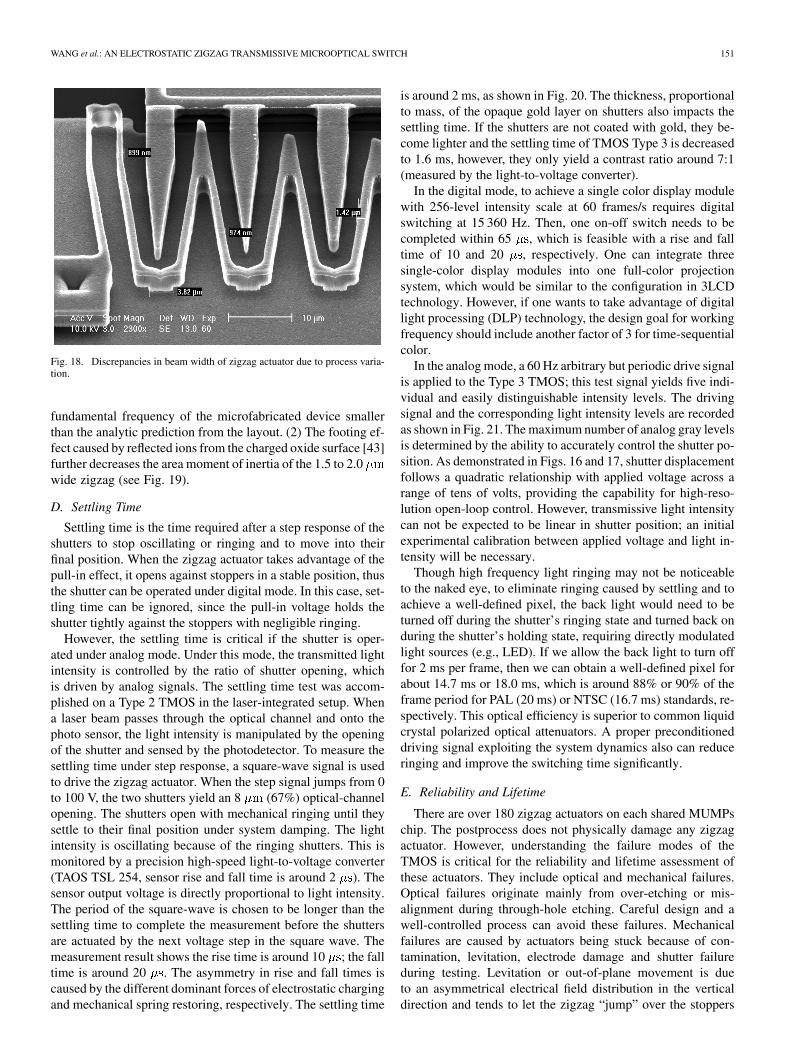
Fig. 18. Discrepancies in beam width of zigzag actuator due to process varia-tion.
fundamental frequency of the microfabricated device smallerthan the analytic prediction from the layout. (2) The footing ef-fect caused by reflected ions from the charged oxide surface [43]further decreases the area moment of inertia of the 1.5 to 2.0wide zigzag (see Fig. 19).
D. Settling Time
Settling time is the time required after a step response of theshutters to stop oscillating or ringing and to move into theirfinal position. When the zigzag actuator takes advantage of thepull-in effect, it opens against stoppers in a stable position, thusthe shutter can be operated under digital mode. In this case, set-tling time can be ignored, since the pull-in voltage holds theshutter tightly against the stoppers with negligible ringing.
However, the settling time is critical if the shutter is oper-ated under analog mode. Under this mode, the transmitted lightintensity is controlled by the ratio of shutter opening, whichis driven by analog signals. The settling time test was accom-plished on a Type 2 TMOS in the laser-integrated setup. Whena laser beam passes through the optical channel and onto thephoto sensor, the light intensity is manipulated by the openingof the shutter and sensed by the photodetector. To measure thesettling time under step response, a square-wave signal is usedto drive the zigzag actuator. When the step signal jumps from 0to 100 V, the two shutters yield an 8 (67%) optical-channelopening. The shutters open with mechanical ringing until theysettle to their final position under system damping. The lightintensity is oscillating because of the ringing shutters. This ismonitored by a precision high-speed light-to-voltage converter(TAOS TSL 254, sensor rise and fall time is around 2 ). Thesensor output voltage is directly proportional to light intensity.The period of the square-wave is chosen to be longer than thesettling time to complete the measurement before the shuttersare actuated by the next voltage step in the square wave. Themeasurement result shows the rise time is around 10 ; the falltime is around 20 . The asymmetry in rise and fall times iscaused by the different dominant forces of electrostatic chargingand mechanical spring restoring, respectively. The settling time
is around 2 ms, as shown in Fig. 20. The thickness, proportionalto mass, of the opaque gold layer on shutters also impacts thesettling time. If the shutters are not coated with gold, they be-come lighter and the settling time of TMOS Type 3 is decreasedto 1.6 ms, however, they only yield a contrast ratio around 7:1(measured by the light-to-voltage converter).
In the digital mode, to achieve a single color display modulewith 256-level intensity scale at 60 frames/s requires digitalswitching at 15 360 Hz. Then, one on-off switch needs to becompleted within 65 , which is feasible with a rise and falltime of 10 and 20 , respectively. One can integrate threesingle-color display modules into one full-color projectionsystem, which would be similar to the configuration in 3LCDtechnology. However, if one wants to take advantage of digitallight processing (DLP) technology, the design goal for workingfrequency should include another factor of 3 for time-sequentialcolor.
In the analog mode, a 60 Hz arbitrary but periodic drive signalis applied to the Type 3 TMOS; this test signal yields five indi-vidual and easily distinguishable intensity levels. The drivingsignal and the corresponding light intensity levels are recordedas shown in Fig. 21. The maximum number of analog gray levelsis determined by the ability to accurately control the shutter po-sition. As demonstrated in Figs. 16 and 17, shutter displacementfollows a quadratic relationship with applied voltage across arange of tens of volts, providing the capability for high-reso-lution open-loop control. However, transmissive light intensitycan not be expected to be linear in shutter position; an initialexperimental calibration between applied voltage and light in-tensity will be necessary.
Though high frequency light ringing may not be noticeableto the naked eye, to eliminate ringing caused by settling and toachieve a well-defined pixel, the back light would need to beturned off during the shutter’s ringing state and turned back onduring the shutter’s holding state, requiring directly modulatedlight sources (e.g., LED). If we allow the back light to turn offfor 2 ms per frame, then we can obtain a well-defined pixel forabout 14.7 ms or 18.0 ms, which is around 88% or 90% of theframe period for PAL (20 ms) or NTSC (16.7 ms) standards, re-spectively. This optical efficiency is superior to common liquidcrystal polarized optical attenuators. A proper preconditioneddriving signal exploiting the system dynamics also can reduceringing and improve the switching time significantly.
E. Reliability and Lifetime
There are over 180 zigzag actuators on each shared MUMPschip. The postprocess does not physically damage any zigzagactuator. However, understanding the failure modes of theTMOS is critical for the reliability and lifetime assessment ofthese actuators. They include optical and mechanical failures.Optical failures originate mainly from over-etching or mis-alignment during through-hole etching. Careful design and awell-controlled process can avoid these failures. Mechanicalfailures are caused by actuators being stuck because of con-tamination, levitation, electrode damage and shutter failureduring testing. Levitation or out-of-plane movement is dueto an asymmetrical electrical field distribution in the verticaldirection and tends to let the zigzag “jump” over the stoppers

152 JOURNAL OF MICROELECTROMECHANICAL SYSTEMS, VOL. 16, NO. 1, FEBRUARY 2007
Fig. 19. (a) SEM photograph showing the footing effect at the bottom side of a Poly1 structure. It is caused by etching of ions reflected from the charged oxidesurface during the MUMPs Poly1 etch. (b) Cross-section diagram of a cantilever shows the mechanism of etching by reflected ions.
Fig. 20. Shutter settling time (Type 2 zigzag actuator pair with gold on shut-ters).
Fig. 21. Light intensity versus 60 Hz arbitrary driving signal (Type 3 zigzagactuator pair without gold on shutters). Voltages between 0 and�80 V (dashedlower curve) and corresponding intensity signals from the photodiode (blackupper curve) are shown. Both signals use the same x-axis.
and stick on the electrodes. This problem can be solved byusing double height Poly1 and Poly2 as zigzag structural layerin order to increase its vertical stiffness.
Among all the tested designs, Type 1 has the weakest mechan-ical strength, and the lowest natural frequency; it stuck to theelectrode occasionally. Type 2 has the strongest structure; how-ever, it requires the highest driving voltage. Type 3 and Type 4
can be driven with relatively low voltage and yield almost fullrange controllable movement; they can be applied in a prac-tical TMOS device. Therefore, the fatigue and reliability testshave been performed on Type 3 and Type 4. For a single zigzagType 3 actuator, after more than under reso-nance frequency (12.6 kHz, range 15 , sinusoidal excitation
, ), no fatigue or frequency shiftshave been observed.
For a dual actuator Type 4 TMOS, after more than(2 kHz, full-range digital switching mode), no de-
fects or shutter damage caused by collision were apparent. Shut-ters actuated for several billion cycles did not show any notice-able mechanical defect such as wear or beam rupture. The con-tact surface was also investigated and no deterioration has beenobserved. The precise shutter movement was monitored underthe strobe-integrated setup. The bounce caused by shutter colli-sion in the closed state was below the limit for optical obser-vations (less than 1 ), which is smaller than the overlap-ping length of the shutters (1.5 ). We did not observe thatshutter-bouncing would cause any shutter engagement withinthe tested frequency range. However, above the fundamental fre-quency, a difference in mass between the two shutters wouldshift the shutter engagement position away from the center ofthe optical tunnel. A 3 3 array of nine shutters (Type 4) hasbeen successfully actuated except for one failed device due toshutter sticking (yield ratio 88.8%). Their typical resonance fre-quency is around 18 kHz with an addressing voltage around 75V.
VI. CONCLUSION AND SUMMARY
The zigzag design conquers the traditional dilemma inmicroactuators: using an electrostatic actuator to generatelarge displacement within a small design space with relativelylow voltage. Zigzag electrostatic actuator designs enhance theforce-to-stiffness ratio for large displacement. Theoretical andexperimental results demonstrate that the zigzag design hasmany advantages. First, it can achieve full range of controllablemotion for stable analog positioning. This is useful for control-ling transmissive light intensity for each pixel in a variety oftuning applications. Second, the stable traveling range (pull-involtage) can be adjusted simply by manipulating the width ofthe zigzag without involving complicated layout rearrange-ments. Thus, zigzag actuators also can be driven under digitalswitch mode. Third, the space-efficient configuration allows
WANG et al.: AN ELECTROSTATIC ZIGZAG TRANSMISSIVE MICROOPTICAL SWITCH 153
the zigzags to be arranged into a densely packed array forhigh-resolution displays or optical data storage systems withlow unit cost. Finally, low-drive current can be achieved withlow-power consumption.
One can package a limited number of microfabricatedTMOS arrays into an individual module, and then assemblethese modules into a big wall display. The tightest arrangement,which aligns TMOS units (size by
) at a 45-degree angle relative to the pixelarray, can achieve an optical tunnel spacing of 125 pitch.However, a less compact packing with optical tunnel spacingof 200 pitch is recommended for integrating control elec-tronics or spacers onto the device side of the TMOS chip.
Integration of the microlens array and TMOS chip into acomplete module is beyond the scope of this paper. A func-tional TMOS display module should consist of a well-alignedmicrolens array and anti-electrostatic shield to achieve goodoptical efficiency and a reliable operating environment. Thepackaged TMOS module should also have good thermal man-agement and durable structure to prevent device damage fromthermal or mechanical stress and unwanted bending.
Low manufacturing cost is crucial for commercialization. Inparticular, using 12 silicon wafers to produce monolithic 12TMOS displays would be prohibitive. Rather, large displayscould be achieved by tiling of smaller TMOS modules. Mi-crolens arrays can focus the light for each module through aTMOS that is substantially smaller than the module itself. Forfurther cost reduction, it is also possible to build the surface-mi-cromachined TMOS directly on glass, quartz, or polymer sub-strates with integrated microlens arrays. Using a transparentsubstrate would eliminate the need for through-hole etching.Tiling the TMOS modules into a wall display with uniformbrightness and hue while avoiding seam artifacts is a significantremaining challenge.
Finally, besides using the TMOS as a display component, thisspace-efficient device also can be useful for other applicationssuch as optic network attenuators.
ACKNOWLEDGMENT
The authors gratefully acknowledge M. Afromowitz and Y.I. Shen for valuable discussions and suggestions. The authorswould like to thank K. Kerkof, K. Nishimura, E. Miller, A.Tombros, G. Holman, and K. Ritala of the Washington Tech-nology Center; D. Qin and G. Golden of the Center for Nan-otechnology at the University of Washington; W. Ciridon andB. Ratner of the University of Washington Engineered Bioma-terials Center, and W. Walker of Oxford Instruments for theirtechnical training and assistance, and M. Esashi, H. Fujita, andO. Tabata for their hospitality during a sabbatical visit at theirlaboratories.
REFERENCES
[1] K. Wang, K. F. Böhringer, M. Sinclair, and G. Starkweather,“Highly space-efficient electrostatic zigzag actuator for transmissivemicro-optic switches,” in Proc. 12th Int. Conf. Solid-State Sensors andActuators (Transducers’03), Boston, MA, 2003.
[2] T. T. King, G. Kletetschka, M. A. Jah, M. J. Li, M. D. Jhabvala, L.L. Wang, M. A. Beamesderfer, A. S. Kutyrev, R. F. Silverberg, D.Rapchun, D. S. Schwinger, G. M. Voellmer, S. H. Moseley, and L. M.Sparr, “Cryogenic characterization and testing of magnetically actu-ated microshutter arrays for the James Webb space telescope,” in Proc.Solid-State Sensor and Actuator Workshop, Hilton Head Island, SC,2004.
[3] J. Kimmel, J. Hautanen, and T. Levola, “Display technologies forportable communication devices,” Proc. IEEE, vol. 90, no. 4, pp.581–586, 2002.
[4] C. W. McLaughlin, “Progress in projection and large-area displays,”Proceedings of the IEEE, vol. 90, no. 4, pp. 521–532, Apr. 2002.
[5] H. Kawamoto, “The history of liquid-crystal displays,” Proc. IEEE,vol. 90, no. 4, pp. 460–500, Apr. 2002.
[6] H. Uchiike and T. Hirakawa, “Color plasma displays,” Proceedings ofthe IEEE, vol. 90, no. 4, pp. 533–539, 2002.
[7] R. H. Friend, “Organic electroluminescent displays,” in Proc. EuroDis-play, Berlin, Germany, 1999.
[8] L. J. Hornbeck and W. E. Nelson, “Bistable deformable mirror device,”in OSA Technical Digest Series: Spatial Light Modulators and Appli-cations, 1988, p. 107.
[9] R. Apte, F. Sandejas, W. Banyai, and D. Bloom, “Grating light valvesfor high resolution displays,” in Solid State Sensors and ActuatorsWorkshop, 1994.
[10] S. Bains, “Micromechanical display uses interferometric modulation,”SPIE Optical Engineering Reports 2000, vol. 199.
[11] [Online]. Available: http://www.parc.com/research/projects/paperdis-plays/2002
[12] A. Biffen, “Understanding HDTV–A Comparison,” 2004 [Online].Available: http://softwareforhomes.com/HDTV-Home-Theatre.htm
[13] H. Urey, “Spot size, depth-of-focus, and diffraction ring intensity for-mulas for truncated Gaussian beams,” Appl. Opt., vol. 43, no. 3, 2004.
[14] R. T. Howe and R. S. Muller, “Resonant-microbridge vapor sensor,”IEEE Trans. Electron Devices, vol. ED-33, pp. 499–506, 1986.
[15] M. A. Schmidt and R. T. Howe, “Resonant microsensors,” in Tech.Dig., 4th Int. Conf. Solid-State Sensor and Actuators, Tokyo, Japan,1987.
[16] W. Newell, “Novel circuit aspects of the resonant gate transistor,” inProc. IEEE Int. Solid-State Circuits Conf., 1966.
[17] P. B. Chu and K. S. J. Pister, “Analysis of closed-loop control of par-allel-plate electrostatic microgrippers,” in Proc. IEEE Conf. Robot. Au-tomat., San Diego, CA, 1995.
[18] J. I. Seeger and S. B. Crary, “Stabilization of electrostatically actuatedmechanical devices,” in Proc. Transducers’97, Chicago, IL, 1997.
[19] E. K. Chan and R. W. Dutton, “Electrostatic micromechanical actuatorwith extended range of travel,” J. Microelectromech. Syst., vol. 9, no.3, pp. 321–328, 2000.
[20] E. S. Hung and S. D. Senturia, “Leveraged bending for full-gap posi-tioning with electrostatic actuation,” in Proc. Solid-State Sensor andActuator Workshop, Hilton Head, SC, 1998.
[21] R. Legtenberg, J. Gilbert, S. D. Senturia, and M. Elwenspoek, “Elec-trostatic curved electrode actuators,” J. Microelectromech. Syst., vol. 6,no. 3, pp. 257–265, 1997.
[22] G. Perregaux, S. Gonseth, P. Debergh, J. P. Thiebaud, and H. Vuil-liomenet, “Arrays of addressable high-speed optical microshutters,” J.Microelectromech. Syst., vol. 10, 2001.
[23] R. Legtenberg, A. W. Groeneveld, and M. Elwenspoek, “Comb-driveactuators for large displacements,” J. Micromech. Microeng., vol. 3, pp.320–329, 1996.
[24] M. Mita, M. Arai, S. Tensaka, D. Kobayashi, and H. Fujita, “A micro-machined impact microactuator driven by electrostatic force,” J. Mi-croelectromech. Syst., vol. 12, no. 1, pp. 37–41, 2003.
[25] M. S. Rodgers, S. Kota, J. Hetrick, Z. Liz, B. D. Jensen, T. W. Kry-gowskil, S. L. Miller, S. M. Barnes, and M. S. Burg, “A new class ofhigh force, low-voltage, compliant actuation systems,” in Proc. Solid-State Sensor and Actuator Workshop, Hilton Head Island, SC, 2000.
[26] R. R. A. Syms, B. M. Hardcastle, and R. A. Lawes, “Bulk microma-chined silicon comb-drive electrostatic actuators with diode isolation,”Sens. Actuators A: Phys., vol. 63, no. 1, pp. 61–67, 1997.
[27] J. T. Nee, K. Y. Lau, and R. S. Muller, “A flat high-frequency scan-ning micromirror,” in Proc. Solid-State Sensor and Actuator Workshop,Hilton Head Island, SC, 2000.
[28] J.-L. A. Yeh, H. Jiang, and N. C. Tien, “Integrated polysilicon andDRIE bulk silicon micromachining for an electrostatic torsional actu-ator,” J. Microelectromech. Syst., vol. 8, no. 4, pp. 456–465, 1999.
154 JOURNAL OF MICROELECTROMECHANICAL SYSTEMS, VOL. 16, NO. 1, FEBRUARY 2007
[29] T. Hirano, T. Furuhata, K. J. Gabriel, and H. Fujita, “Design, fabrica-tion, and operation of submicron gap comb-drive microactuators,” J.Microelectromech. Syst., vol. 1, no. 1, pp. 52–59, 1992.
[30] M. A. Rosa, S. Dimitrijev, and H. B. Harrison, “Improved operationof microelectromechanical comb-drive actuators through the use of anew angled comb finger design,” in Proc. SPIE Conf. Smart Materials,Structures, and MEMS, 1997.
[31] W. Ye, S. Mukherjee, and N. C. MacDonald, “Optimal shape designof an electrostatic comb drive in microelectromechanical systems,” J.Microelectromech. Syst., vol. 7, no. 1, pp. 16–26, 1998.
[32] W. Ye and S. Mukherjee, “Design and fabrication of an electrostaticvariable gap comb drive in micro-electro-mechanical systems,” Proc.ASME Micro-Electro-Mechanical Systems (MEMS), vol. 66, pp.537–544, 1998.
[33] B. D. Jensen, S. Mutlu, S. Miller, K. Kurabayashi, and J. J. Allen,“Shaped comb fingers for tailored electromechanical restoring force,”J. Microelectromech. Syst., vol. 12, no. 3, pp. 373–383, 2003.
[34] A. L. Pisano and Y. H. Cho, “Mechanical design issues in laterally-driven microstructures,” in Proc. Transducers’89, Montreux, Switzer-land, 1989.
[35] W. C. Tang, T. H. Nguyen, and R. T. Howe, “Laterally driven polysil-icon resonant microstructures,” Sens. Actuators A: Phys., vol. A 20, pp.25–32, 1989.
[36] J. Grade, H. Jerman, and T. Kenny, “Design of large deflection electro-static actuator,” J. Microelectromech. Syst., vol. 12, no. 3, pp. 335–343,2003.
[37] J. M. Gere and S. P. Timoshenko, Mechanics of Materials, 3rd ed.Boston, MA: PWS-Kent, 1990.
[38] C. F. Beards, Structural Vibration Analysis and Damping. Oxford,U.K.: Butterworth-Heinemann, 1996, p. 105C. F. Beards, StructuralVibration Analysis and Damping 1996, p. 105.
[39] [Online]. Available: http://www.ansoft.com[40] D. A. Koester, R. Mahadevan, H. B. , and K. W. Markus, MUMPs
Design Handbook. Milpitas, CA: JDS Uniphase, 2001.[41] B. Schwartz and H. Robbins, “Chemical etching of silicon, IV. Etching
technology,” J. Electrochem. Soc., vol. 123, no. 12, pp. 1903–1909,1976.
[42] R. d’Agostino, Ed., Plasma Deposition, Treatment, and Etching ofPolymers. Boston, MA: Academic, 1990.
[43] A. A. Ayon, S. Nagle, L. Frechette, A. Epstein, and M. A. Schmidt,“Tailoring etch directionality in a deep reactive ion etching tool,” J.Vac. Sci. Technol., vol. B18, no. 3, pp. 1412–1416, 2000.
Kerwin Wang received the B.S. degree in me-chanical engineering from Chung Yuan ChristianUniversity, Taiwan, the M.S. degree in mechanicalengineering from the State University of New Yorkat Buffalo, NY, and the Ph.D. degree in electricalengineering from the University of Washington,Seattle, in 2004.
During his dissertation work on micro-displaymodules, he invented, modeled, and tested zigzagactuators and floating sliders; he also held an intern-ship from Microsoft Research, Redmond, WA. Upon
completion of his Ph.D. degree, he spent a year as a Postdoctoral Researcherat the University of Washington, where he investigated micro/nanoassemblytechniques. In July 2005, he was hired as a Visiting Postdoctoral Researcherat the Intel Component Research Group and developed high-packing-densitymicro-assembly for solid-state cooling applications.
Michael Sinclair received the undergraduate andgraduate degrees in electrical engineering from theGeorgia Institute of Technology (Georgia Tech),Atlanta.
He worked for a while for Western Electric andthen joined the research team at Georgia Tech.There, except for a brief interlude to help start andgrow a flight simulation company, he has worked inmany aspects of hardware research including radar,optics, high-powered lasers, data acquisition, missilesimulation, bioelectronics, surgical simulation,
telemedicine, and robotics. He was Director of the Multimedia ResearchLab that was instrumental in helping Atlanta win the right to host the 1996Olympics. He joined Microsoft’s Research group in 1998 as a Sr. Researcher.One of his recent interests at Microsoft is in the field of MEMS (micro-electromechanical systems) as a possible solution to a number of interfaceproblems.
Gary K. Starkweather received the B.S. degreein physics from Michigan State University, EastLansing, in 1960 and the Master’s degree in opticsfrom the University of Rochester, Rochester, NY, in1966.
He has spent over 40 years in the imaging sciencesand holds over 44 patents in the fields of imaging,color, and hardcopy devices. From 1962 to 1964, heworked for Bausch & Lomb, Inc., Rochester. From1964 until 1988, he was employed by Xerox Corpo-ration, where he became a Senior Research Fellow.
While at the Xerox Palo Alto Research Center, or PARC, he invented the laserprinter. From 1988 until 1997, he was employed by Apple Computer as an AppleFellow involved in Publishing and Color Imaging products and research. He ispart of Microsoft Research as an Architect working on displays and informationprocessing. He has published many papers and has written a book chapter enti-tled, “High Speed Laser Printers” (New York: Academic). He continues to serveon several technical committees involved in display and color-related imagingissues. He has lectured at both Stanford University and UCLA.
Mr. Starkweather has received a number of awards for this work, includingthe Xerox President’s Achievement Award (1977), the Johann Gutenberg Prizefrom the Society for Information Display (1987), and the David Richardsonmedal from the Optical Society of America (1991). In 1994, he received a Tech-nology Academy Award for his consulting work with Lucasfilm and Pixar oncolor film scanning. In 2002, he was inducted into the Technology Hall of Fameat COMDEX.
Karl F. Böhringer (S’94–M’97–SM’03) receivedthe Dipl.-Inform. degree from the University ofKarlsruhe, Germany, in 1990 and the M.S. and Ph.D.degrees in computer science from Cornell University,Ithaca, NY, in 1993 and 1997, respectively.
From 1994 to 1995, he was a Visiting Scholar atStanford University, Stanford, CA, and from 1996 to1998, he was a Postdoctoral Researcher at the Univer-sity of California, Berkeley. He joined the ElectricalEngineering Department at the University of Wash-ington in Seattle, WA, in 1998, where he currently
Associate Professor. He also held visiting faculty positions at the Universitiesof Tohoku, Tokyo, Kyoto, Japan, and São Paulo, Brazil. His research interestsinclude microelectromechanical systems (MEMS), manipulation and assemblyfrom macro- to nanoscales, microfluidic systems for the life sciences, and mi-crorobotics. He has created, among others, multibatch self-assembling systems,massively parallel microactuator arrays, and a walking microrobot.
Dr. Böhringer is a member of the Society for Nanoscale Science, Computingand Engineering (ISNSCE), the American Society for Information Sciences(GI). He was awarded a Long-Term Invitational Fellowship for Research inJapan by the Japan Society for the Promotion of Science (JSPS) in 2004, anIEEE Robotics and Automation Society Academic Early Career Award in 2004,an NSF CAREER Award in 1999, and an NSF Postdoctoral Associateship in1997. His work was listed among the “Top 10 Science Stories of 2002” inDiscover magazine. He is an Associate Editor for the IEEE/ASME JOURNAL
OF MICROELECTROMECHANICAL SYSTEMS and the IEEE TRANSACTIONS ON
AUTOMATION SCIENCE AND ENGINEERING, and has served, among others, ontechnical program committees for IEEE MEMS and Transducers conferences.

![JOURNAL OF MICROELECTROMECHANICAL SYSTEMS, VOL. 15, …€¦ · genated alkylsiloxane monolayers such as octadecyltrichlorosilane (OTS). [1637] Index Terms—Microelectromechanical](https://img.dokumen.tips/doc/110x75/606226c6f2c83655de52c35d/journal-of-microelectromechanical-systems-vol-15-genated-alkylsiloxane-monolayers.jpg)