Embed Size (px)
Citation preview
1.3MPxl High Speed CMOS Image Sensor
LUPA-1300
Cypress Semiconductor Corporation • 198 Champion Court • San Jose, CA 95134-1709 • 408-943-2600Document Number: 38-05711 Rev. *C Revised January 4, 2007
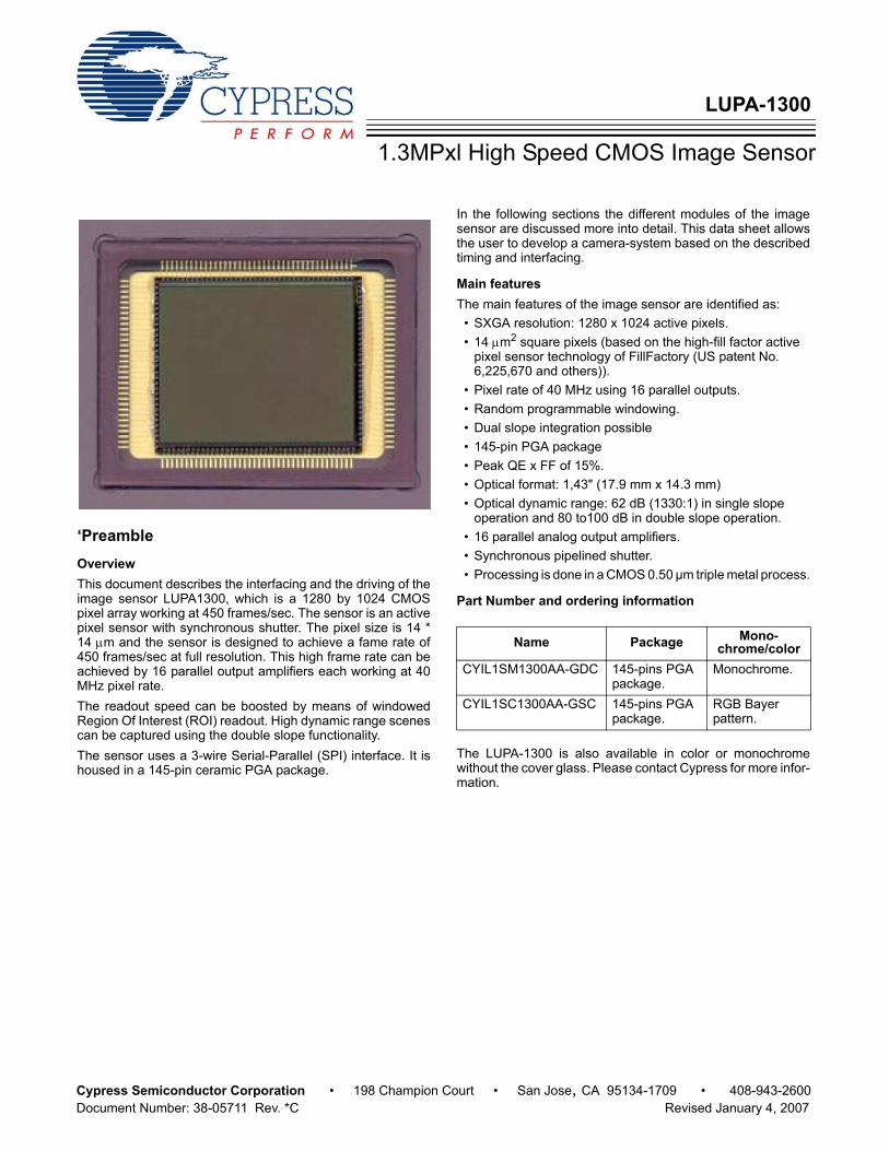
‘PreambleOverviewThis document describes the interfacing and the driving of theimage sensor LUPA1300, which is a 1280 by 1024 CMOSpixel array working at 450 frames/sec. The sensor is an activepixel sensor with synchronous shutter. The pixel size is 14 *14 µm and the sensor is designed to achieve a fame rate of450 frames/sec at full resolution. This high frame rate can beachieved by 16 parallel output amplifiers each working at 40MHz pixel rate. The readout speed can be boosted by means of windowedRegion Of Interest (ROI) readout. High dynamic range scenescan be captured using the double slope functionality. The sensor uses a 3-wire Serial-Parallel (SPI) interface. It ishoused in a 145-pin ceramic PGA package.
In the following sections the different modules of the imagesensor are discussed more into detail. This data sheet allowsthe user to develop a camera-system based on the describedtiming and interfacing.
Main featuresThe main features of the image sensor are identified as:
• SXGA resolution: 1280 x 1024 active pixels.• 14 µm2 square pixels (based on the high-fill factor active
pixel sensor technology of FillFactory (US patent No. 6,225,670 and others)).
• Pixel rate of 40 MHz using 16 parallel outputs.• Random programmable windowing.• Dual slope integration possible• 145-pin PGA package• Peak QE x FF of 15%.• Optical format: 1,43" (17.9 mm x 14.3 mm)• Optical dynamic range: 62 dB (1330:1) in single slope
operation and 80 to100 dB in double slope operation.• 16 parallel analog output amplifiers.• Synchronous pipelined shutter.• Processing is done in a CMOS 0.50 µm triple metal process.
Part Number and ordering information
The LUPA-1300 is also available in color or monochromewithout the cover glass. Please contact Cypress for more infor-mation.
Name Package Mono-chrome/color
CYIL1SM1300AA-GDC 145-pins PGA package.
Monochrome.
CYIL1SC1300AA-GSC 145-pins PGA package.
RGB Bayer pattern.

LUPA-1300
Document Number: 38-05711 Rev. *C Page 2 of 32
TABLE OF CONTENTS
Preamble ........................................................................................................................................................... 1Specifications ................................................................................................................................................... 4
Overview ...................................................................................................................................................... 4Features and general specifications ............................................................................................................ 5Spectral response curve .............................................................................................................................. 5Photo-voltaic response curve ....................................................................................................................... 6Absolute maximum ratings ........................................................................................................................... 6Recommended operating conditions ........................................................................................................... 7
Sensor architecture .......................................................................................................................................... 8Frame rate calculation ................................................................................................................................. 10X-Y addressing and windowing .................................................................................................................... 10Temperature diode ....................................................................................................................................... 10Temperature module .................................................................................................................................... 10Power supplies and grounds ........................................................................................................................ 12Biasing and analog signals .......................................................................................................................... 14Pixel array signals ........................................................................................................................................ 14Digital signals ............................................................................................................................................... 15Test signals .................................................................................................................................................. 15
Timing ................................................................................................................................................................ 16Reduced Row Overhead Time timing .......................................................................................................... 18
Pin configuration .............................................................................................................................................. 20Pad positioning and packaging ...................................................................................................................... 25
Monochrome ................................................................................................................................................ 27Color ............................................................................................................................................................ 28Handling precautions ................................................................................................................................... 28
Application notes & FAQ ................................................................................................................................. 30APPENDIX A: LUPA-1300 Evaluation kit ........................................................................................................ 31Document History Page ................................................................................................................................... 32
LIST OF FIGURESSpectral response curve ..................................................................................................................................... 5Output voltage as a function of the number of electrons. ................................................................................... 6Architecture of the LUPA sensor ........................................................................................................................ 8Schematic representation of the synchronous pixel as used in the LUPA design .............................................. 8Schematic representation of the column readout structure. ............................................................................... 9Schematic representation of a single output stage ............................................................................................. 9Output voltage of the temperature module versus temperature ......................................................................... 11Synchronous shutter operation ........................................................................................................................... 11Integration and read out in parallel ..................................................................................................................... 12Principle of non-destructive readout. .................................................................................................................. 12Figure11a. Schematic of typical decoupling of power supply (source current) .................................................. 13Figure 11b.Schematic of typical decoupling of power supply (source current) .................................................. 13Internal timing of the pixel. .................................................................................................................................. 14Timing of the pixel array ...................................................................................................................................... 16

LUPA-1300
Document Number: 38-05711 Rev. *C Page 3 of 32
Timing of the y shift register. .............................................................................................................................. 17Readout time of a line is the sum of the row blanking time and on the line readout time. .................................. 17Reduced standard ROT by means of Sh_col signal............................................................................................ 18Only pre_col and Norowsel control signals are required. SH_col is made active low. ....................................... 19Schematic of the SPI interface ........................................................................................................................... 19Package drawing of the LUPA-1300 sensor ....................................................................................................... 25Package drawing with die of the LUPA-1300 sensor ......................................................................................... 26Color filter arrangement on the pixels. ................................................................................................................ 27Transmission characteristics of the D263 glass used as protective cover for the LUPA-1300 sensors. ............ 27Transmission characteristics of the S8612 glass used as NIR cut-off filter. ....................................................... 28Dual slope diagram ............................................................................................................................................. 30
LIST OF TABLESGeneral specifications of the LUPA sensor ........................................................................................................ 4Electrical-optical specifications of the LUPA-1300 sensor ................................................................................. 4Features and general specifications ................................................................................................................... 5Absolute maximum ratings ................................................................................................................................. 6Recommended operation conditions .................................................................................................................. 7Advantages and disadvantages of non-destructive readout. .............................................................................. 12Power supplies used in the LUPA design ........................................................................................................... 13Overview of biasing signals ................................................................................................................................ 14Overview of the internal and external pixel array signals. .................................................................................. 15Typical timings of the pixel array ........................................................................................................................ 16Pin description of the assembled LUPA-1300 sensor in the PGA 144 package. ............................................... 21

LUPA-1300
Document Number: 38-05711 Rev. *C Page 4 of 32
SpecificationsGeneral specifications
Electro-optical characteristics
Overview
Table 1. General specifications of the LUPA sensor
Parameter Specification RemarksPixel architecture 6T-pixel Based on the high-fill factor active pixel sensor technology of
FillFactoryPixel size 14 µm x 14 µm The resolution and pixel size results in a 17.9 mm x 14.3 mm optical
active area.Resolution 1280 x1024 Pixel rate 640 MHz Using a 20 MHz system clock and 16 parallel outputs.Shutter type Pipelined snapshot shutter Full snapshot shutter with variable integration timeFull frame rate 450 frames/second Frame rate increase possible with ROI read out and/or sub sampling.Package Pin grid array 145 pins PGA pins with 0.46 mm diameter
Table 2. Electrical-optical specifications of the LUPA-1300 sensor
Parameter Specification RemarksFPN <3% RMS <10% p/p.PRNU 2% RMS Half saturation.Conversion gain 16 uV/electronOutput signal amplitude 1V Unity gain.Saturation charge 62.500 e- Is more then 60.000 (=1V/16uV/e-) due to non-linearity in saturated
region.Sensitivity 1500 V.m2/W.s Average white light.
8.33 V/lux.s Visible band only (180 lx = 1 W/m2).21.43 V/lux.s Visible + NIR (70 lx = 1 W/m2).
Fill Factor 50% 100%-metal and polycide coverage.Peak QE * FF Peak SR * FF
15%0.08 A/W
See spectral response curve.
MTF X: 67%Y: 66%
@ Nyquist
Temporal Noise 45e- Dark environment, measured at T=21 oC. S/N ratio 1330 1330 = 60000:45 = 62 dB.Spectral sensitivity range 400 - 1000 nmParasitic light sensitivity < 0.5% I.e. sensitivity of the storage node compared to the sensitivity of
photodiodePower dissipation 900 mWatt Typical.Output impedance 200-300 Ohms Typical

LUPA-1300
Document Number: 38-05711 Rev. *C Page 5 of 32
Features and general specifications
Spectral response curve
Figure 1. Spectral response curve
Figure 1 shows the spectral response characteristic. Thecurve is measured directly on the pixels. It includes effects ofnon-sensitive areas in the pixel, e.g. interconnection lines. The
sensor is light sensitive between 400 and 1000 nm. The peakQE * FF is 15% approximately between 500 and 700 nm.
Table 3. Features and general specifications
Feature Specification/DescriptionElectronic shutter type Synchronous pipelined shutter with variable integration time.Windowing (ROI) Programmable via SPI.Read out sequence Progressive scan.Extended dynamic range Double slope extended dynamic range.X clock 20 MHz (pixel rate of 40 MHz)Number of outputs 16.Supply voltage VDD Image core supply: Range from 3V to 6 V.
Analog supply: Nominal 5 V.Digital: Nominal 5 V.
Logic levels 5V (digital supply)Operational temperature range 0°C to 60°C, with degradation of dark current.Package 145-pins Pin Grid Array (PGA).
0
0.02
0.04
0.06
0.08
0.1
0.12
400 500 600 700 800 900 1000
Wavelength (nm)
Response(A/W)
QE=10%
QE=15%
QE= 20%
LUPA-1300

LUPA-1300
Document Number: 38-05711 Rev. *C Page 6 of 32
Photo-voltaic response curve
Figure 2. Output voltage as a function of the number of electrons
As one can see from Figure 2, the output signal rangesbetween 0 V to 1.1 V and is linear until around 800 mV. Note
that the upper part of the curve (near saturation) is actually alogarithmic response.
Electrical specifications
Absolute maximum ratings
Note1. Absolute Ratings are those values beyond which damage to the device may occur.
Table 4. Absolute maximum ratings
Symbol Parameter Value UnitVDC DC supply voltage -0.5 to +7 VVIN DC input voltage 0.5 to VDC + 0.5 VVOUT DC output voltage -0.5 to VDC + 0.5 VI DC current per pin; any single input or output. (see
Table 7 for more exceptions)± 50 mA
TSTG Storage temperature range. -40 to 100 °CTL Lead temperature (10 seconds soldering). 300 °C

LUPA-1300
Document Number: 38-05711 Rev. *C Page 7 of 32
Recommended operating conditions
Notes2. All parameters are characterized for DC conditions after thermal equilibrium has been established.3. Unused inputs must always be tied to an appropriate logic level, e.g. either VDD or GND.4. This device contains circuitry to protect the inputs against damage due to high static voltages or electric fields; however it is recommended that normal precautions
be taken to avoid application of any voltages higher than the maximum rated voltages to this high impedance circuit.5. All power supplies should be sufficiently decoupled because spikes and drops in the power supplies will be immediately visible in the analog output signals.
Table 5. Recommended operation conditions
Symbol Parameter Typ UnitVdda Power supply column read out module. 5 VVdd Power supply digital modules 5 VVddr Power supply logic for drivers 5 VVoo Power supply output stages 5 VVres Power supply reset drivers 6 VVres_ds Power supply multiple slope reset driver 4.5 VVmem_h Power supply memory element (high level) 6 VVmem_l Power supply memory element (low level) 4.5 VVpix Power supply pixel array 4.5 VVstable Power supply output stages. Decouples noise on the Voo supply from the
output signal. 5.5 V

LUPA-1300
Document Number: 38-05711 Rev. *C Page 8 of 32
Sensor architectureThe image sensor consists of the pixel array, the columnreadout electronics, X-and Y addressing, on chip drivers, theoutput amplifiers and some logic
Figure 3. Architecture of the LUPA sensor.
Figure 3 shows a schematic representation of the imagesensor on which the different modules are displayed.The image core is a pixel array of 1280 * 1024 pixels each of14 *14 µm2 in size. The readout is from bottom left to top right.To obtain a frame rate of 450 frames/sec for this resolution, 16output amplifiers each capable of driving an output capaci-tance of 10 pF at 40 MHz are placed on the image sensor. The column readout amplifiers bring the pixel data to theoutput amplifiers. The logic and the x- and y addressingcontrols the image sensor so that progressive scan andwindowing is possible. Extra pixel array drivers are foreseenat the top of the image sensor to control the global pixel arraysignals.
Pixel architectureThe active pixels allow synchronous shutter i.e. all pixels areilluminated during the same integration time, starting from thesame moment in time. After a certain integration time, thepixels are readout sequentially. Readout and integration are inparallel, which means that when the image sensor is readout,the integration time for the next frame is ongoing. This featurerequires a memory element inside the pixel, which affects the
maximum fill factor. A schematic representation of the pixel isgiven in Figure 4
Figure 4. Schematic representation of the synchronous pixel as used in the LUPA design
X-addressing
Analog multiplexer
Column amplifiers
Pixel core
Pixel
Output
amplifiers
Imager core
SPI interface
Sensor
Y-addressing
System clock
40 MHz
3
2
1
16
15
14
Drivers for the pixel array signals Control signals
precharge
reset sampleRow
select
Columnout
Vpix
Mem
Note6. The signals mentioned in Figure 4 are the internal signals, generated by the internal drivers, required to have the synchronous shutter feature

LUPA-1300
Document Number: 38-05711 Rev. *C Page 9 of 32
The photodiode is designed to obtain sensitivity as high aspossible for a dynamic range of at least 60dB. Consequentlythe photodiode capacitance is 10 fF @ the output, resulting ina S/N of more than 60 dB as the rms noise level is within theexpectation of 45 noise electrons. The pixel was speciallydesigned to have a very low parasitic light sensitivity (<0.5%).The pixels are based on the high-fill factor active pixel sensortechnology of FillFactory (US patent No. 6,225,670 andothers)).
Column readout amplifiersThe column readout amplifiers are the interface between thepixels and the output amplifiers. The pixels in the array areselected line by line and the pixels of the selected line areconnected to the column readout amplifiers, which bring thepixel data in the correct format to the output amplifiers.
To obtain a high frame rate, the complexity and the number ofstages in the column readout amplifiers must be minimized, sothat the power dissipation remains as low as possible, but alsoto minimize the row blanking time. Figure 5 is a schematicrepresentation of the column readout structure. It consists of 2parts. The first part is a module that reduces the row blankingtime. The second part shifts the signal to the correct level forthe output amplifiers and allows multiplexing in the x-direction. From the moment that a new row is selected, the pixel data ofthat row is placed onto the columns of the pixel array. Thesecolumns are long lines and have a large parasitic capacitance.As the pixel is small, it is not possible to match the transistorinside the pixel, which drives this column. Consequently, thefirst module in the column readout amplifiers must solve themismatch between the pixel driver and the large columncapacitance
Figure 5. Schematic representation of the column readout structure
Output amplifiers16 output amplifiers each capable of working at 40 MHz pixelrate are placed equidistant on the bottom of the image sensor.These output amplifiers are required to obtain a frame rate of
450 frames/sec. A single output stage, not only to reducepower, but also to achieve the required pixel rate is designed.Figure 6 is a schematic representation of this module
Figure 6. Schematic representation of a single output stage.
Each output stage is designed to drive a load of 10 pF at a pixelrate of 40 MHz. The load in the output stage determines thispixel rate. In case the load capacitance is less than 10 pF, theload in the output stage can increase, resulting in less power
dissipation of the output stages and consequently of the wholesensor. Additionally, decreasing the load of the output stageallows having more current available for the output stage to
Output stage
column
Module 1 : track & hold or reference set method
Module 2 : signal conditioning and multiplexing X-mux
Shkol
Norow sel
Stabilizepower supply
Vstable
In Out
Output stage
Cload 10pF

LUPA-1300
Document Number: 38-05711 Rev. *C Page 10 of 32
charge or discharge the load capacitance to obtain a higherpixel rate. To avoid variations on the supply voltage to be seen on theoutput signal, a special module to stabilize the power supplyis required. This module that requires an additional supply
voltage (Vstable) allows variation on the supply voltage Voowithout being seen on the output signal. One can also choose to have a passive load of chip instead ofthe active output stage load. This deteriorates the linearity ofthe output stages, but decreases the power dissipation, as thedissipation in the load is external.
Frame rate and windowing
Frame rate calculationThe frame period of the LUPA-1300 sensor can be calculatedas follows:Frame period = FOT + (Nr.Lns* (RBT + pixel period * Nr. Pxs/16) with:FOT: Frame Overhead Time = 1 us.Nr. Lns: Number of Lines read out each frame (Y).Nr. Pxs: Number of pixels read out each line (X).RBT: Row blanking time = 200 ns (nominal; can be further reduced).Pixel period: clock_x period/2 (both rising and falling edge are active edges). - Example 1 read out of the full resolution at nominal speed (40 MHz pixel rate):Frame period = 5 us + (1024 * (200 ns + 25 ns * 1280/16) = 2.25 ms => 444 fps.- Example 2 read out of 800x600 at nominal speed (40 MHz pixel rate):Frame period = 5 us + (600 * (200 ns + 25 ns * 800/16) = 871 us => 1148 fps.- Example 3 read out of 640x480 at nominal speed (40 MHz pixel rate):Frame period = 5 us + (480 * (200 ns + 25 ns * 640/16) = 577 us => 1733 fps.- Example 4 read out of the full resolution at nominal speed (40 MHz pixel rate) with reduced overhead time:Frame period = 5 us + (1024 * (100 ns + 25 ns * 1280/16) = 2.15 ms => 465 fps.
X-Y addressing and windowingThe pixel array is readout by means of programmable X andY shift registers. The pixel array is scanned line-by-line andcolumn-by-column. The starting point in X and Y is definedindividually for each register and is determined by the addressdownloaded by the Serial-Parallel Interface (SPI). Bothregisters work in the same way. A sync pulse that sets theaddress pointer to the starting address of each register,initializes them. A clock pulse for the x- and y-shift registershifts the pointer individually and makes sure that thesequential selection of the lines and columns is correct.
Temperature reference circuits
Temperature diodeThe most commonly used temperature measurement ismonitoring of the junction voltage of a diode, therefore we alsoadded a temperature diode to measure the temperature of thesilicon die. This diode junction voltage is generated by a"small", forward biased, constant current flow (in between 10and 100 µA). This junction voltage has a nearly linear relationship with thetemperature of the die with a typical sensitivity of about 430°Cper volt (2.3 mV per °C) for silicon junctions.
Temperature moduleOn the same image sensor we have foreseen a module toverify the temperature on chip and the variation of the outputvoltage (dark level of the pixel array) due to a temperaturevariation. This module contains a copy of the complete signalpath, including a blind pixel, the column amplifiers and anoutput stage. It DC response may serve a temperaturecalibration for the real signal. The temperature functionality isgiven in Figure 7. Between room temperature and 60oC wesee a voltage variation of about 0.5 mV.Due to different applied supply voltages, as there are: Vreset,Vmem, Vpix an offset between the output voltage of thetemperature sensor and the output of a black signal of the pixelarray can occur. Depending on the working conditions of theimage sensor one can fine-tune the temperature module withits voltage supply. In case one has a 6V signal for reset and a4-6V signal for Vmem, a supply voltage of 5.5V for the temper-ature sensor will result in a closer match between this temper-ature sensor and the black level of the image sensor.Changing the supply voltage of the temperature sensor resultsonly in a shift of the output voltage therefore the supply voltageof the temperature module can be tuned to make the output ofthe module equal to the dark signal of the pixel array at acertain working temperature.
Note7. The LUPA-1300 is designed to drive a capacitive load, not a resistive. When one wants to transport the output signals over long distances (more than 1 inch),
make sure to place buffers on the outputs with high input impedances (preferably >1Mohms). This is necessary because the output impedance of the LUPA-1300 is between 200-300 ohms typically.

LUPA-1300
Document Number: 38-05711 Rev. *C Page 11 of 32
Figure 7. Output voltage of the temperature module versus temperature
Synchronous shutterIn a synchronous (snapshot) shutter light integration takesplace on all pixels in parallel, although subsequent readout issequential
Figure 8. Synchronous shutter operation.
Figure 8 shows the integration and read out sequence for thesynchronous shutter. All pixels are light sensitive at the sameperiod of time. The whole pixel core is reset simultaneously
and after the integration time all pixel values are sampledtogether on the storage node inside each pixel. The pixel coreis read out line by line after integration.
Vsupply (V) 5 5.5 6 6.1 6.2 6.3 6.4 6.5
Vout @ 21 oC 0.58 0.8 1.03 1.07 1.12 1.17 1.22 1.27
0.99
1.01
1.03
1.05
1.07
1.09
1.11
1.13
25 35 45 55 65 75
Temperature (°C)
Vout(V)
6
6.1
6.2
Time axis
Line number
Integration time Burst Readout time
COMMONRESET
COMMONSAMPLE&HOLD
Flashcouldoccurhere
Note8. Note that the integration and read out cycle can occur in parallel.

LUPA-1300
Document Number: 38-05711 Rev. *C Page 12 of 32
Figure 9. Integration and read out in parallel
The control of the readout of the frame and of the integrationtime are independent of each other with the only exception thatthe end of the integration time from frame I+1 is the beginningof the readout of frame I+1.
Non-destructive readout (NDR)The sensor can also be read out in a non-destructive way. Aftera pixel is initially reset, it can be read multiple times, withoutresetting. The initial reset level and all intermediate signals canbe recorded. High light levels will saturate the pixels quickly,but a useful signal is obtained from the early samples. For lowlight levels, one has to use the later or latest samples.
Figure 10. Principle of non-destructive readout.
Essentially an active pixel array is read multiple times, andreset only once. The external system intelligence takes careof the interpretation of the data. Table 6 summarizes theadvantages and disadvantages of non-destructive readout.
Operation and signalingOne can distinguish the different signals into different groups:
• Power supplies and grounds• Biasing and analog signals• Pixel array signals• Digital signals• Test signals
Power supplies and groundsEvery module on chip, as there are: column readout, outputstages, digital modules, drivers, has its own power supply andground. Off chip the grounds can be combined, but not allpower supplies may be combined. This results in severalpower supplies, but is required to reduce electrical crosstalkand to improve shielding.On chip we have the ground lines also separately for everymodule to improve shielding and electrical crosstalk betweenthem. The only special ground is "Gnd_res", which can beused to remove the blooming if any and which can improveoptical crosstalk.An overview of the supplies is given in Table 7. The powersupplies related to the pixel array signals are described in theparagraph concerning the pixel array signals.
Integration I + 2
Read frame I + 1
Integration I + 1
Read frame I
time
Table 6. Advantages and disadvantages of non-destruc-tive readout.
Advantages DisadvantagesLow noise - as it is true CDS. System memory required to
record the reset level and the intermediate samples.
High sensitivity - as the conversion capacitance is kept rather low.
Requires multiples readings of each pixel, thus higher data throughput.
High dynamic range - as the results includes signal for short and long integrations times.
Requires system level digital calculations.
Note9. Normal application doesn't require this Gnd_res and it can be connected to ground.

LUPA-1300
Document Number: 38-05711 Rev. *C Page 13 of 32
The maximum currents mentioned in Table 7 are peakcurrents. The power supplies need to be able to deliver thesecurrents especially the maximum supply current for Vpix.It is important to notice that we don't do any power supplyfiltering on chip and that noise on these power supplies can
contribute immediately to the noise on the signal. Especiallythe voltage supplies Vpix and Vdda are important to be wellnoise free. With respect to the power supply Voo, a specialdecoupling is used, for which an additional power supplyVstable is required
Figure 11a. Schematic of typical decoupling of power supply (source current)
Figure 11b. Schematic of typical decoupling of power supply (source current)
Table 7. Power supplies used in the LUPA design
Name Max current Typ. Max DescriptionVdda 50 mA 5V Power supply column readout moduleVdd 20 mA 5V Power supply digital modulesVoo 85 mA 5V Power supply output stagesVstable 6 mA 5.5V 6V Power supply output stages. Decouples noise on the Voo
supply from the output signal. Vpix 200 mA 4.5V 6V Power supply pixel array.Vddr 20 mA 5V Power supply logic for driversVres 50 mA 6V Power supply to reset the pixelsVmemH 50 mA 6V Power supply for high DC level VmemVmemL 50 mA 4.5V Power supply for low DC level Vmem
Notes10. At start up the Vpix supply draws a very high current (> 300 mA) which has to be limited (max. 200 mA) otherwise the bond wires of the particular supply will
be destroyed. One should make sure that the Vpix power supply limits the current draw to the Vpix sensor supply pins to max. 200 mA. When the bond wires of Vpix are destroyed the sensor isn't operating normally and will not meet the described specifications.
11. VmemL must sink a current, not source it. All power supplies should be decoupled very close to the sensor pin (typical 100nF to filter high frequency dips and 10 microF to filter slow dips). A typical decoupling circuit is shown in the figure below. Vres_ds must be able to sink and source current.

LUPA-1300
Document Number: 38-05711 Rev. *C Page 14 of 32
Biasing and analog signalsBesides the biasing signals, the only analog signals are theoutput signals Out1 - Out16. Each output signal is analog withrespect to the voltage level, but is discrete in time. This meansthat on the speed of Clock_x, the outputs change to a differentlevel, depending on the illumination of the correspondingpixels.The biasing signals determine the speed and power dissi-pation of the different modules on chip. These biasing signalshave to be connected trough a resistor to ground or power
supply and should be decoupled with a capacitor. If the sensoris working properly, each of the biasing signals will have adc-voltage depending on the resistor value and on the internalcircuitry. These dc-voltages can be used to check theoperation of the image sensor. Table 8 gives the differentbiasing signals, the way they should be connected, and theexpected dc-voltage. Due to small process variations, thesedc-voltages change from chip to chip and 10% variation ispossible.
Each resistor controls the speed and power dissipation of thecorresponding module, as this resistor determines the currentrequired to charge and/or discharge internal nodes inside themodule. A decoupling with a small capacitor is advisable to reduce theHF noise onto the analog signals. Only the capacitor on thePre_load signal can be omitted.
Pixel array signalsFigure 4 in paragraph 2.2 is a schematic representation of thepixel as used in the LUPA design. The applied signals to thispixel are: reset, sample, Precharge, Vmemory, row select andVpix. These are internal generated signals derived by on chipdrivers from external applied signals. Consequently it isimportant to understand the relation between both internal andexternal signals and to understand the operation of the pixel.The timing of the pixel is given in Figure 12 in which only theinternal signals are given.
Figure 12. Internal timing of the pixel.
At the end of the integration time, the information on the photo-diode node needs to be sampled and stored onto the pixelmemory, required to allow synchronous shutter. To do this,we need the signals "Precharge" and "Sample". "Precharge"resets the pixel memory and "Sample" places the pixel infor-mation onto the pixel memory. Once this information stored,the readout of the pixel memories can start in parallel with a
new integration time. An additional signal "Vmem" is neededto obtain a larger output swing. Except from Vpix power supply, drivers generate the otherpixel signals on chip. The external signals to obtain therequired pulses consist of 2 groups. One is the group of digitalsignals to indicate when the pulse must occur and the othergroup is dc-supply lines indicating the levels of the pulses.
Table 8. Overview of biasing signals
Signal Comment Expected dc-level
Pre_load Connect with 10 KΩ to Vdda and capacitor of 100 nF to Gnd 2.0V
Col_load Connect with 2 MΩ to Vdda and capacitor of 100 nF to Gnd 0.9V
Psf_load Connect with 240 KΩ to Gnd and capacitor of 100 nF to Vdda 3.7V
Nsf_load Connect with 100 KΩ to Vdda and capacitor of 100 nF to Gnd 1.3V
Load_out Connect with 27 KΩ to Voo and capacitor of 100 nF to Gnd 1.6V
Decx_load Connect with 27 KΩ to Gnd and capacitor of 100 nF to Vdd 2.8V
Decy_load Connect with 27 KΩ to Gnd and capacitor of 100 nF to Vdd 2.8V

LUPA-1300
Document Number: 38-05711 Rev. *C Page 15 of 32
Table 9 summarizes the relation between the internal andexternal pixel array signals
The Precharge and Sample signals are the most straight-forward signals. The internal signal Vmemory is a signal thatswitches between a low voltage (3.5 - 5.5V) and a high voltage(5-6V). The signal Mem_hl controls the applied level and thepower supply lines Vmem_l and Vmem_h determine the lowand high dc-levels. The Reset signal is due to the dual slope technique a littlemore complex. In case the dual slope is not used, the resetsignal is straightforward generated from the external resetpulse. In this case the supply voltage Vres determines thelevel to which the pixel is resetted.In case the dual slope operation is desired, one needs to givea second pulse to a lower reset level during integration. Thiscan be done by the control signal Reset_ds and by the powersupply Vres_ds that defines the level to which the pixel has tobe resetted.If a pulse is given on the Reset_ds signal, a second pulse onthe internal reset line is generated to a lower level, determinedby the supply Vres_ds. If no Reset_ds pulse is given, the dualslope technique is not implemented. Note that Reset is dominant over Reset_ds, which means thatthe high voltage level will be applied for reset, if both pulsesoccur at the same time. The external control signals should be capable of driving inputcapacitance of about 20 pF.
Digital signalsThe digital signals control the readout of the image sensor.These signals are:
• Sync_y: Starts the readout of the frame or window at the address defined by the y-address register. This pulse synchronizes the y-address register: active high. This signal is at the same time the end of the frame or window and determines the window width.
• Clock_y: Clock of the y-register. On the rising edge of this clock, the next line is selected.
• Sync_x: Starts the readout of the selected line at the address defined by the x-address register. This pulse synchronizes the x-address register: active high. This signal is at the same time the end of the line and determines the window length.
• Address: the x- and y-address is downloaded serial through this signal.
• Clock_spi: clock of the serial parallel interface. This clock downloads the address into the SPI register.
• Load_addr: when the SPI register is downloaded with the desired address, the signal Load_addr signal loads the x-and y-address into their address register as starting point of the window of interest.
• Sh_col: control signal of the column readout. Is only used in sample & hold mode (See timing)
• Norow_sel: Control signal of the column readout. Is only used in Norow_sel mode (See timing)
• Pre_col: Control signal of the column readout to reduce row blanking time
• Sel_active: activates the active load on chip for the output amplifiers. If not used, a passive load can be used or one can use this signal to put the output stages in standby mode
• Eos_x: end of scan signal: is an output signal, indicating when the end of the line is reached. Is not generated when doing windowing
• Eos_y: end of scan signal: is an output signal, indicating when the end of the frame is reached. Is not generated when doing windowing.
All digital signals are buffered and filtered on chip to removespikes and to achieve the required on chip driving speed. Theapplied digital signals should be capable of driving 20 pF inputcapacitance.
Test signalsSome test signals are required to evaluate the optical perfor-mance of the image sensor. Other test signals allow us to testinternal modules in the image sensor and some test signalswill give us information concerning temperature and influenceof the temperature on the black level. Evaluation on the optical performance (Spectral response, fillfactor)• Array_diode• Full_diode
Evaluation of the output stages:• Black• Dc_black
Evaluation of the x and y -shift registers:• Eos_x• Eos_y
Indication of the temperature and influence on the black level:• Temp_diode_n• Temp_diode_p
Table 9. Overview of the internal and external pixel array signals.
Internal signal Vlow Vhigh External control signal Low dc level High dc level
Precharge 0 5V Precharge Gnd VddrSample 0 5V Sample Gnd VddrReset 0V 4 - 6V Reset & Reset_ds Gnd_res Vres & Vres_dsVmemory 4.5V 6V Mem_hl Vmem_l Vmem_h

LUPA-1300
Document Number: 38-05711 Rev. *C Page 16 of 32
TimingTiming of the pixel arrayThe timing of the image sensor can be divided in two majorparts. The first part of the timing is related with the timing ofthe pixel array. This implies the control of the integration time,the synchronous shutter operation, and the sampling of the
pixel information onto the memory element inside each pixel.The signals needed for this control are described earlier andFigure 12 shows the timing of the internal signals. Figure 13should make the timing of the external signals clear.
Figure 13. Timing of the pixel array. All external signals are digital signals between 0 and 5V. The Reset_ds is only required in case dual slope is desired
The timing of the pixel array is straightforward. Before theframe is read, the information on the photodiode needs to bestored onto the memory element inside the pixels. This is doneby means of the signals Vmemory, Precharge and Sample.Precharge sets the memory element to a reference level andSample stores the photodiode information onto the memoryelement. Vmemory pumps up this value to reduce the loss ofsignal in the pixel and this signal must be the envelop ofPrecharge and Sample. After Vmemory is high again, thereadout of the pixel array can start. The frame blanking time orframe overhead time is thus the time that Vmemory is low,which is about 5 sec. Once the readout starts, the photodiodescan all be initialised by reset for the next integration time. Theduration of the reset pulse indicates the integration time for thenext frame. The longer this duration, the shorter the integrationtime becomes. Maximum integration time is thus the time ittakes to readout the frame, minus the minimum pulse for reset,which is preferred not to be less than 10 sec. The minimalintegration time is the minimal time between the falling edgeof reset and the rising edge of sample. Keeping the slow fall
times of the corresponding internal generated signals, aminimal integration time is about 2 sec. An additional resetpulse can be given during integration by Reset_ds toimplement the double slope integration mode.
Readout of the pixel arrayOnce the photodiode information is stored into the memoryelement in each pixel, the total pixel array of 1280 * 1024needs to be readout in less than 2 msec (2 msec - frameoverhead time = 1995 µsec). Additionally, it is possible thatonly a part of the whole frame is read out. This is controlled bythe starting address that has to be downloaded and from theend address, which is controlled by the synchronisation pulsesin x- and y direction. The readout itself is straightforward. Lineby line is selected by means of a sync-pulse and by means ofa Clock_y signal. Once a new line selected, it takes a while(row blanking time) before the information of that line is stable.After this row blanking time the data is multiplexed in blocks of16 to the output amplifiers. A sync-pulse and a clock pulse inthe x-direction do this multiplexing.
Table 10. Typical timings of the pixel array
Symbol Name Valuea Mem_HL > 5 µsecb MEM_HL -Precharge > 200 nsecc Precharge > 500 nsecd Sample > 3.9 µsece Precharge-Sample > 400 nsecf Integration time > 2 µsec

LUPA-1300
Document Number: 38-05711 Rev. *C Page 17 of 32
Figure 14 shows the y-address timing. The top curves are theselection signals of the pixels, which are sequentially active,starting by the sync pulse. The next line is selected on the
rising edge of Clock_y. It is important that the Sync_y pulsecovers 1 rising edge of the Clock_y signal. Otherwise thesynchronization will not work properly.
Figure 14. Timing of the y shift register
The first selected line after a Sync_y pulse is the line definedby the y-address in the y-address register. Every select line isin principle 1 clock period long, except for the first select line.The first select line goes high as soon as a Sync_y pulseoccurs together with a rising edge of Clock_y. On the nextrising edge of Clock_y, the next row is selected, unless Sync_y
is still active. In Figure 15, a short Sync_y pulse makes surethat the first row is selected during 1 period of Clock_y. Once a line is selected, it needs to stabilize first of all, which iscalled the row blanking time, and secondly the pixels need tobe read out. Figure 15 shows the principle.
Figure 15. Readout time of a line is the sum of the row blanking time and on the line readout time.
Symbol Name Value
a Sync_Y > 100 nsec
b Sync_Y-Clock_Y > 50 nsec
c Clock_Y-Sync_Y > 50 nsec
d Sync_X -Clock_X > 50 ns
Notes13. The applied Clock_x, is filtered on chip to remove spikes. This is especially required at these high speeds. This filtering results in an on chip Clock_x that is
delayed in time with about 10 nsec. In other words, the data at the output has, with respect to the external Clock_x, a propagation delay of 20 nsec. This 20 nsec come from 10 nsec of the generation of the internal Clock_x and 10 nsec due to other on chip generated signals.
14. The analog signal will come out of the sensor with a 60/40 duty cycle. Therefore it is very important to have a very flexible ADC clock phase. This is necessary to fine-tune the ADC to sample the analog signal at the correct moment.

LUPA-1300
Document Number: 38-05711 Rev. *C Page 18 of 32
Once the information of the selected line is stable theaddressing of the pixels can start. This is done by means of aSync_x and a Clock_x pulse in the same way as theY-addressing. The Sync_x pulse downloads the address in theaddress register into the shift register and connects the firstblock of 16 columns to the 16 outputs.In fact on chip is a 32-output bus instead of 16, but on the risingedge of Clock_x the first 16 columns of the bus are connectedto the output stages. On the falling edge of Clock_x, the last16 columns of the selected bus are connected to the outputstages. The timing of the x-shift register is comparable with the timingof the y-shift register, only that the timing is much faster. Againthe synchronization pulse must be high on the rising edge ofClock_x.
Reduced Row Overhead Time timingThe row overhead time is the time between the selection oflines that one has to wait to get the data stable at the columnamplifiers.
This row overhead time is a loss in time, which should bereduced as much as possible.
Reduced timingA straightforward way of reducing the R.O.T is by using asample and hold function. By means of Sh_col the analog data is tracked during the first200 nsec during the selection of a new set of lines. After 200nsec, the analog data is stored. The ROT is in this casereduced to 200 nsec, but as the internal data was not stableyet dynamic range is lost because not the complete analoglevels are reached yet after 200ns.Figure 16 shows this principle. Sh_col is now a pulse of100ns-200ns starting 25 ns after Norowsel. The duration ofSh_col is equal to the ROT. The shorter this time the shorterthe ROT will be however this lowers also the dynamic range.
Figure 16. Reduced standard ROT by means of Sh_col signal. pre_col (short pulse), Norowsel (short pulse) and Sh_col (large pulse).

LUPA-1300
Document Number: 38-05711 Rev. *C Page 19 of 32
Standard timing (ROT = 200 ns
Figure 17. Only pre_col and Norowsel control signals are required. SH_col is made active low.)
In this case the control signals Norowsel and pre_col are madeactive for about 50 nsec from the moment the next line isselected. The time these pulses have to be active is relatedwith the biasing resistance Pre_load. The lower this resis-tance, the shorter the pulse duration of Norowsel and pre_colmay be. After these pulses are given, one has to wait for 180nsec before the first pixels can be sampled. For this modeSh_col must be made active low.
Timing of the Serial Parallel Interface (SPI)The serial parallel interface is used to upload the x- andy-address into the x- and y-address registers. This address isthe starting point of the window of interest and is uploaded inthe shift register by means of the corresponding synchroni-zation pulse. The elementary unit cell of the serial to parallel interface isshown in Figure 18. 16 of these cells are connected in parallel,having a common Load_addr and Clock_spi form the entireuploadable address block. The uploaded addresses areapplied to the sensor on the rising edge of signal Load_addr.
Figure 18. Schematic of the SPI interface
The SPI clock can have a frequency of 20 MHz and the datais loaded into the register at the rising edge. The load_addr
pulse should go high together or after the last falling edge ofthe SPI_clock (see Figure 18).
D Q
C
D Q
C
Address_in
To address registers
Address_out
Clock_spi
Load_address
16 outputs to sensor : 6 x-address
bits and 10 y-address bits
Clock_spi
Address
Unity Cell
E ntire uploadable address blockLoad_addr
A1 A2 A3 A16
Load_addr
Clock_spi
address
command
applied to
sensor

LUPA-1300
Document Number: 38-05711 Rev. *C Page 20 of 32
The Y-address has to be applied first and the X-address last.With respect to the timing in Figure 18, A1 corresponds withthe least significant bit of the Y-address (Y0) and A16 corre-sponds with the most significant bit of the X-address (X5). TheY-address is a 10 bit and the X-address is a 6-bit addressregister.If the X-address register is 6-bit wide this means that 64 valuescan be uploaded in this register. The X-start position howevercan only be adjusted with steps of 32 so only the 40 LSB's areaccepted by the internal decoder (32 x 40=1280). TheY-address register is 10 bit wide (1024 values), so the Y-startaddress can be adjusted on a line by line basis.
Start-upWhen starting the sensor the following sequence should befollowed:1. Apply all power supplies.2. Upload SPI register.3. Start driving/clocking of the sensor.One should make sure that the power supplies are completelystable before the SPI is uploaded and the driving of the sensorcan start.

LUPA-1300
Document Number: 38-05711 Rev. *C Page 21 of 32
Pin configurationThe LUPA-1300 sensor will be packed in a PGA package with145 pins. Each bond pad consists of 2 pad openings, one for
wafer probing and one for bonding. Table 11 gives an overviewof the pin names and their functionality.
Table 11. Pin description of the assembled LUPA-1300 sensor in the PGA 144 package
Pin fp Name Function DescriptionB3 1 n.c. Not connectedC3 2 n.c.D3 3 Voo Supply 5V Supply voltage output stages: 5V A2 4 Gnd Ground Ground of the sensorB2 5 Out1 Analog out Output 1E3 6 Voo Supply 5V Supply voltage output stages: 5V C2 7 Out2 Analog out Output 2D2 8 Gnd Ground Ground of the sensorE2 9 Out3 Analog out Output 3A1 10 Voo Supply 5V Supply voltage output stages: 5V F3 11 Out4 Analog out Output 4F2 12 Gnd Ground Ground of the sensorB1 13 Out5 Analog out Output 5C1 14 Voo Supply 5V Supply voltage output stages: 5V D1 15 Out6 Analog out Output 6G3 16 Gnd Ground Ground of the sensorE1 17 Out7 Analog out Output 7G2 18 Voo Supply 5V Supply voltage output stages: 5V F1 19 Out8 Analog out Output 8G1 20 Gnd Ground Ground of the sensorH3 21 Out9 Analog out Output 9H2 22 Voo Supply 5V Supply voltage output stages: 5VH1 23 Out10 Analog out Output 10J1 24 Gnd Ground Ground of the sensorJ2 25 Out11 Analog out Output 11J3 26 Voo Supply 5V Supply voltage output stages: 5VK1 27 Out12 Analog out Output 12K2 28 Gnd Ground Ground of the sensorL1 29 Out13 Analog out Output 13K3 30 Voo Supply 5V Supply voltage output stages: 5VL2 31 Out14 Analog out Output 14M1 32 Gnd Ground Ground of the sensorN1 33 Out15 Analog out Output 15L3 34 Voo Supply 5V Supply voltage output stages: 5VM2 35 Out16 Analog out Output 16P1 36 Gnd Ground Ground of the sensorN2 37 Voo Supply 5V Supply voltage output stages: 5VM3 38 n.c.P2 39 n.c.

LUPA-1300
Document Number: 38-05711 Rev. *C Page 22 of 32
N3 40 Gnd Ground Ground of the sensorN4 41 Voo Supply 5V Supply voltage output stages: 5VN5 42 Vstable Supply 5V Supply voltage to stabilize output stages: 5.5VP3 43 Load_out Biasing Analog bias for output amplifiers 27 KΩ to Voo and
capacitor of 100 nF to groundP5 44 Dc_black Testpin 6 dc-black signal required to characterize the output
stagesP4 45 Vdd Supply 5V Supply voltage digital modules: 5VQ1 46 Gnd Ground Ground of the sensorN6 47 Vdda Supply 5V Supply voltage analog modules: 5VP6 48 Gnd Ground Ground of the sensorQ2 49 Vpix Supply 4.5V Supply voltage pixel array: 4.5VQ3 50 Eos_x Digital I/O End of scan signal of the x-register: active high pulse
indicates the end of the shift register is reachedQ4 51 Nsf_load Biasing Analog bias for column stages: 100 KΩ to Vdda and
capacitor of 100nF to groundN7 52 Psf_load Biasing Analog bias for column stages: 240 KΩ to gnd and
capacitor of 100 nF to VddaP7 53 Col_load Biasing Analog bias for column stages: 2 MΩ to Vdda and
capacitor of 100 nF to groundQ5 54 Pre_load Biasing Analog bias for column stages: 10 KΩ to Vdda and
capacitor of 100 nF to groundQ6 55 n.c.Q7 56 Array_diode Testpin 3 Array of pixels as designed in pixel array N8 57 Full_diode Testpin 4 Full diode with same array as array diode: 140 * 70 µm2
P8 58 Temp_diode_p Testpin 1 Temperature diode p sideQ8 59 Temp_diode_n Testpin 2 Temperature diode n sideQ9 60 n.c.P9 61 n.c.N9 62 n.c.Q10 63 n.c.Q11 64 n.c.Q12 65 n.c.P10 66 n.c.N10 67 n.c.Q13 68 n.c.P11 69 Vpix Supply 4.5V Supply voltage pixel array: 4.5VP12 70 Gnd Ground Ground of the sensorN11 71 Vddr Supply 5V Supply voltage of the logic for the drivers: 5VN12 72 n.c.P13 73 Vmem_l Supply Voltage supply for Vmemory drivers: 3V- 5V (typ: 4.5V)N13 74 Vmem_h Supply Voltage supply for Vmemory drivers: 4V- 6V (typ. 6V)M13 75 Vres_ds Supply Voltage supply for reset double sloped drivers: 4V - 5V Q14 76 Vres Supply Voltage supply for reset drivers: 5V - 6V (typ 6V)P14 77 Gnd_res Ground_ab Ground anti-blooming: 0 - 1V
Table 11. Pin description of the assembled LUPA-1300 sensor in the PGA 144 package (continued)
Pin fp Name Function Description

LUPA-1300
Document Number: 38-05711 Rev. *C Page 23 of 32
L13 78 n.c.N14 79 n.c.M14 80 n.c.L14 81 n.c.Q15 82 n.c.K13 83 n.c.K14 84 n.c.P15 85 n.c.N15 86 n.c.M15 87 n.c.J13 88 n.c.L15 89 n.c.J14 90 n.c.K15 91 n.c.J15 92 n.c.H13 93 n.c.H14 94 Gnd Ground Ground for temperature moduleH15 95 Temp Testpin 5 Dark level signal as function of temperature (Figure 7)G15 96 Vdd Supply Supply voltage temperature module: 5V (has to be
tunable to adjust output of temperature module to analog output)
G14 97 n.c.G13 98 n.c.F15 99 n.c.F14 100 n.c.E15 101 Reset_ds Digital I/O Double slope reset of the pixels: active high pulseF13 102 Reset Digital I/O Reset signal of the pixels: active high pulseE14 103 Mem_hl Digital I/O Control of Vmemory signal: 5V: Vmem_h, 0V: Vmem_lD15 104 Sample Digital I/O Samples the photodiode voltage onto the memory cell
inside each pixel: active high pulseC15 105 Precharge Digital I/O Precharge the memory cell inside the pixel: active high
pulseE13 106 Eos_y Digital I/O End of scan signal of the y-register: active high pulse
indicates the end of the shift register is reachedD14 107 Gnd_Res Ground_ab Ground for the reset drivers. Can be used as
anti-blooming by applying 1V instead of 0VB15 108 Vres Supply Voltage supply for reset drivers: 5V - 6V (typ: 6V)C14 109 Vres_ds Supply Voltage supply for reset double sloped drivers: 4V - 5V D13 110 Vmem_h Supply Voltage supply for Vmemory drivers: 5V- 6V (typ: 6V)B14 111 Vmem_l Supply Voltage supply for Vmemory drivers: 3V- 5V (typ: 4.5V)C13 112 Vddr Supply 5V Supply voltage of the logic for the drivers: 5VC12 113 Vpix Supply 4.5V Supply voltage pixel array: 4.5VC11 114 Vdd Supply 5V Supply voltage digital modules: 5VB13 115 Gnd Ground Ground of the sensor
Table 11. Pin description of the assembled LUPA-1300 sensor in the PGA 144 package (continued)
Pin fp Name Function Description

LUPA-1300
Document Number: 38-05711 Rev. *C Page 24 of 32
B11 116 n.c.B12 117 n.c.A15 118 n.c.C10 119 n.c.B10 120 n.c.A14 121 n.c.A13 122 n.c.A12 123 n.c.C9 124 n.c.B9 125 n.c.A11 126 Load_addr Digital I/O Loads the address into the serial parallel interface (SPI)A10 127 Address Digital I/O Serial address to be downloaded into the SPIA9 128 Clock_spi Digital I/O Clock for the SPIC8 129 Decy_load Digital I/O Bias for y address register: 27KΩ to ground and
capacitor of 100 nF to VddB8 130 Sync_y Digital I/O Synchronisation of y-address register: active highA8 131 Clock_y Digital I/O Clock of y-address registerA7 132 Norow_sel Digital I/O Control signal for Norow_sel mode to reduce row
blanking time: active lowB7 133 Sh_col Digital I/O Control signal for Sh_col mode to reduce row blanking
time: active low (baseline method): active low C7 134 Pre_col Digital I/O Additional control signal for reducing the row blanking
timeA6 135 Sync_x Digital I/O Synchronisation of the x-address register: active highA5 136 Clock_x Digital I/O Clock of the x-address registerA4 137 Decx_load Biasing Bias for x address register: 27 KΩ to ground and
capacitor of 100 nF to VddB6 138 Black Digital I/O Controls black test function of the output stages: active
high, connect to ground if not usedC6 139 Sel_active Digital I/O set the output stages active or in standby mode: active
lowA3 140 Vdd Supply 5V Supply voltage digital modules: 5VB5 141 Gnd Ground Ground of the sensorB4 142 Vdda Supply 5V Supply voltage analog modules: 5VC5 143 Gnd Ground Ground of the sensorC4 144 Voo Voo Supply voltage output stages: 5V
Table 11. Pin description of the assembled LUPA-1300 sensor in the PGA 144 package (continued)
Pin fp Name Function Description

LUPA-1300
Document Number: 38-05711 Rev. *C Page 25 of 32
Pad positioning and packagingPackage
Figure 19. Package drawing of the LUPA-1300 sensor
A B C D E F G H J K L M N P Q
12
34
56
78
910
11
12
13
14
15
25,62
19,5
40,01
40,01
R1,27
B
DetailBscale4/1
R1,27
0,90 0,90
C
DetailCscale4/1
23,5
0,25
1,02 0,51
2,80
SECTION
A-A'
A
A'
2,54
35,56
note1
~
note:
1.dieattachareashouldbemetallizedand
connectedtopadnumberD4 alldimensionsinmm
Ø 1,78
29,62
1,274,57
0,20
4x0,5
R 1
17,5
23,62

LUPA-1300
Document Number: 38-05711 Rev. *C Page 26 of 32
Package and die
Figure 20. Package drawing with die of the LUPA-1300 sensor
The center of the pixel array is located 200 µm to the right and51 µm above the center of the package. The first pixel is
located at 9160 µm to the left and 7219 to the bottom from thiscenter. All distances are with a deviation of 50 µm.

LUPA-1300
Document Number: 38-05711 Rev. *C Page 27 of 32
Color filterAn optional color filter can be processed as well.
The LUPA-1300 can also be processed with a Bayer RGBcolor pattern. Pixel (0,0) has a red filter.
Figure 21. Color filter arrangement on the pixels.
Glass transmittance
MonochromeA D263 glass will be used as protection glass lid on top of theLUPA-1300 monochrome sensors.Figure shows the trans-mission characteristics of the D263 glass
Figure 22. Transmission characteristics of the D263 glass used as protective cover for the LUPA-1300 sensors
0
10
20
30
40
50
60
70
80
90
100
400 500 600 700 800 900
Wavelength [nm]
Transmission[%]

LUPA-1300
Document Number: 38-05711 Rev. *C Page 28 of 32
ColorFor color devices a near infrared attenuating color filter glassis used. The dominant wavelength is around 490 nm.Figure 23 shows the transmittance curve for the glass.
A S8612 glass will be used as NIR cut-off filter on top of theLUPA-1300-C color image sensor. Figure 24 shows the trans-mission characteristics of the S8612 glass.
Figure 23. Transmission characteristics of the S8612 glass used as NIR cut-off filter.
Handling and Storage precautions
Handling precautionsSpecial care should be given when soldering image sensorswith color filter arrays (RGB color filters), onto a circuit board,since color filters are sensitive to high temperatures.Prolonged heating at elevated temperatures may result indeterioration of the performance of the sensor. The followingrecommendations are made to ensure that sensor perfor-mance is not compromised during end-users' assemblyprocesses.
Board Assembly:Device placement onto boards should be done in accordancewith strict ESD controls for Class 0, JESD22 Human BodyModel, and Class A, JESD22 Machine Model devices.Assembly operators should always wear all designated andapproved grounding equipment; grounded wrist straps at ESDprotected workstations are recommended including the use ofionized blowers. All tools should be ESD protected.
Manual Soldering:When a soldering iron is used the following conditions shouldbe observed:• Use a soldering iron with temperature control at the tip.• The soldering iron tip temperature should not exceed
350°C.• The soldering period for each pin should be less than 5
seconds.
Precautions and cleaning:Avoid spilling solder flux on the cover glass; bare glass andparticularly glass with antireflection filters may be adverselyaffected by the flux. Avoid mechanical or particulate damageto the cover glass.It is recommended that isopropyl alcohol (IPA) be used as asolvent for cleaning the image sensor glass lid. When usingother solvents, it should be confirmed beforehand whether thesolvent will dissolve the package and/or the glass lid or not.

LUPA-1300
Document Number: 38-05711 Rev. *C Page 29 of 32
Storage conditions
Ordering Information
DisclaimerFillFactory image sensors are only warranted to meet thespecifications as described in the data sheet. Specificationsare subject to change without notice.
Description Minimum Maximum Units ConditionsTemperature –10 66 °C @ 15% RHTemperature –10 38 °C @ 86% RH
FillFactory Part Number Cypress Semiconductor Part NumberLUPA-1300-C CYIL1SC1300AA-GACLUPA-1300-M CYIL1SM1300AA-GBC
Note15. RH = Relative Humidity

LUPA-1300
Document Number: 38-05711 Rev. *C Page 30 of 32
Application notes & FAQQ: Can the LUPA-1300 directly drive an ADC?A: Yes, coupling the LUPA-1300 to a set of 16 ADC's close to the chip is the preferred way of operation. A suitable ADC musthave thus
• Input range equal or larger than the 1.2 V- 0 V sensor signal swing• In view of the LUPA-1300's S/N 10 bits are suitable. 11 or 12 bits may be considered too.• Input capacitance 20 pF or lower (high output loads will limit the speed). And no significant resistive loading.• Sampling frequency 40 MHz (or the application specific sample rate)• The ADC's input bandwidth must be sufficiently higher than the sampling frequency, in order to avoid RC contamination between
successive pixels.Q: How does the dual slope extended dynamic range mode works?A:
Figure 24. Dual slope diagram
The green lines are the analog signal on the photodiode, which decrease as a result of exposure. The slope is determined by theamount of light at each pixel (the more light the steeper the slope). When the pixels reach the saturation level the analog signalwill not change despite further exposure. As you can see without any double slope pulse pixels p3 and p4 will reach saturationbefore the sample moment of the analog values, no signal will be acquired without double slope. When double slope is enableda second reset pulse will be given (blue line) at a certain time before the end of the integration time. This double slope reset pulseresets the analog signal of the pixels BELOW this level to the reset level. After the reset the analog signal starts to decrease withthe same slope as before the double slope reset pulse. If the double slope reset pulse is placed at the end of the integration time(90% for instance) the analog signal that would have reach the saturation levels aren't saturated anymore (this increases theoptical dynamic range) at read out. It's important to notice that pixel signals above the double slope reset level will not beinfluenced by this double slope reset pulse (p1 and p2).Please look at our website to find some pictures taken with the double slope mode on:http://www.fillfactory.be/htm/technology/htm/dual-slope.htm
p4
p3
p2
p1
Reset level 1
Reset level 2
Saturation level
Total integration time
ResetDouble slope reset
Read
Double slope reset time (usually 5-10% of the totalintegration time)

LUPA-1300
Document Number: 38-05711 Rev. *C Page 31 of 32© Cypress Semiconductor Corporation, 2006. The information contained herein is subject to change without notice. Cypress Semiconductor Corporation assumes no responsibility for the useof any circuitry other than circuitry embodied in a Cypress product. Nor does it convey or imply any license under patent or other rights. Cypress products are not warranted nor intended to beused for medical, life support, life saving, critical control or safety applications, unless pursuant to an express written agreement with Cypress. Furthermore, Cypress does not authorize itsproducts for use as critical components in life-support systems where a malfunction or failure may reasonably be expected to result in significant injury to the user. The inclusion of Cypressproducts in life-support systems application implies that the manufacturer assumes all risk of such use and in doing so indemnifies Cypress against all charges. All products and company namesmentioned in this document may be trademarks of their respective holders.
APPENDIX A: LUPA-1300 Evaluation kitFor evaluating purposes a LUPA-1300 evaluation kit isavailable. The LUPA-1300 evaluation kit consists of a multifunctionaldigital board (memory, sequencer and IEEE 1394 Fire Wireinterface), an ADC-board and an analog image sensor board.
Visual Basic software (under Win 2000 or XP) allows thegrabbing and display of images and movies from the sensor.All acquired images and movies can be stored in different fileformats (8 or 16-bit). All setting can be adjusted on the fly toevaluate the sensors specs. Default register values can beloaded to start the software in a desired state.
Please contact Fillfactory ([email protected]) if you wantany more information on the evaluation kit.All products and company names mentioned in this document may be the trademarks of their respective holders.

LUPA-1300
Document Number: 38-05711 Rev. *C Page 32 of 32
Document History Page
Document Title: LUPA-1300 1.3MPxl High Speed CMOS Image SensorDocument Number: 38-05711
REV. ECN. Issue Date Orig. of Change Description of Change
** 310396 See ECN SIL Initial Cypress release*A 370756 See ECN FPW Additional timing specifications and removal of inconsistencies throughout the
data sheet*B 497127 See ECN QGS Converted to Frame file*C 649105 See ECN FPW Updated ordering information