Embed Size (px)
Citation preview

CY7C64215enCoRe™ III Full Speed USB Controller
Cypress Semiconductor Corporation • 198 Champion Court • San Jose, CA 95134-1709 • 408-943-2600Document 38-08036 Rev. *C Revised December 08, 2008
Features ■ Powerful Harvard Architecture Processor
❐ M8C Processor Speeds to 24 MHz❐ Two 8x8 Multiply, 32-bit Accumulate❐ 3.0V to 5.25V Operating Voltage❐ USB 2.0 USB-IF certified. TID# 40000110❐ Operating Temperature Range: 0°C to +70°C
■ Advanced Peripherals (enCoRe™ III Blocks)❐ 6 Analog enCoRe III Blocks provide:
• Up to 14-bit Incremental and Delta-Sigma ADCs❐ Programmable Threshold Comparator❐ 4 Digital enCoRe III Blocks provide:
• 8-bit and 16-bit PWMs, timers and counters• I2C Master• SPI Master or Slave• Full Duplex UART• CYFISNP and CYFISPI modules to talk to Cypress CYFI
radio
■ Complex Peripherals by Combining Blocks
■ Full-Speed USB (12 Mbps)❐ Four Unidirectional Endpoints❐ One Bidirectional Control Endpoint❐ Dedicated 256 Byte Buffer❐ No External Crystal Required❐ Operational at 3.0V – 3.6V or 4.35V – 5.25V
■ Flexible On-Chip Memory❐ 16K Flash Program Storage 50,000 Erase/Write Cycles❐ 1K SRAM Data Storage❐ In-System Serial Programming (ISSP)❐ Partial Flash Updates❐ Flexible Protection Modes❐ EEPROM Emulation in Flash
■ Programmable Pin Configurations❐ 25-mA Sink on all GPIO❐ Pull up, Pull down, High- Z, Strong, or Open Drain Drive
Modes on all GPIO❐ Configurable Interrupt on all GPIO
■ Precision, Programmable Clocking❐ Internal ±4% 24 and 48 MHz Oscillator❐ Internal Oscillator for Watchdog and Sleep❐ 0.25% Accuracy for USB with no External Components
■ Additional System Resources❐ I2C™ Slave, Master, and Multi-Master to 400 kHz❐ Watchdog and Sleep Timers❐ User-Configurable Low Voltage Detection❐ Integrated Supervisory Circuit❐ On-Chip Precision Voltage Reference
■ Complete Development Tools❐ Free Development Software (PSoC® Designer™)❐ Full-Featured, In-Circuit Emulator and Programmer❐ Full Speed Emulation❐ Complex Breakpoint Structure❐ 128K Bytes Trace Memory
enCoRe III Core
Block Diagram
[+] Feedback [+] Feedback
CY7C64215
Document 38-08036 Rev. *C Page 2 of 30
Applications■ PC HID devices
❐ Mouse (Optomechanical, Optical, Trackball)❐ Keyboards❐ Joysticks
■ Gaming❐ Game Pads❐ Console Keyboards
■ General Purpose❐ Barcode Scanners❐ POS Terminal❐ Consumer Electronics❐ Toys❐ Remote Controls❐ USB to Serial
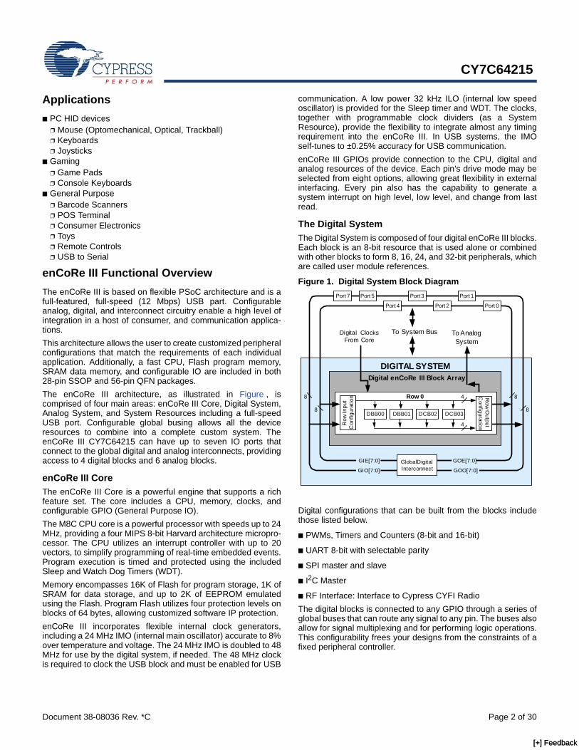
enCoRe III Functional OverviewThe enCoRe III is based on flexible PSoC architecture and is afull-featured, full-speed (12 Mbps) USB part. Configurableanalog, digital, and interconnect circuitry enable a high level ofintegration in a host of consumer, and communication applica-tions.This architecture allows the user to create customized peripheralconfigurations that match the requirements of each individualapplication. Additionally, a fast CPU, Flash program memory,SRAM data memory, and configurable IO are included in both28-pin SSOP and 56-pin QFN packages.The enCoRe III architecture, as illustrated in Figure , iscomprised of four main areas: enCoRe III Core, Digital System,Analog System, and System Resources including a full-speedUSB port. Configurable global busing allows all the deviceresources to combine into a complete custom system. TheenCoRe III CY7C64215 can have up to seven IO ports thatconnect to the global digital and analog interconnects, providingaccess to 4 digital blocks and 6 analog blocks.
enCoRe III CoreThe enCoRe III Core is a powerful engine that supports a richfeature set. The core includes a CPU, memory, clocks, andconfigurable GPIO (General Purpose IO).The M8C CPU core is a powerful processor with speeds up to 24MHz, providing a four MIPS 8-bit Harvard architecture micropro-cessor. The CPU utilizes an interrupt controller with up to 20vectors, to simplify programming of real-time embedded events.Program execution is timed and protected using the includedSleep and Watch Dog Timers (WDT).Memory encompasses 16K of Flash for program storage, 1K ofSRAM for data storage, and up to 2K of EEPROM emulatedusing the Flash. Program Flash utilizes four protection levels onblocks of 64 bytes, allowing customized software IP protection.enCoRe III incorporates flexible internal clock generators,including a 24 MHz IMO (internal main oscillator) accurate to 8%over temperature and voltage. The 24 MHz IMO is doubled to 48MHz for use by the digital system, if needed. The 48 MHz clockis required to clock the USB block and must be enabled for USB
communication. A low power 32 kHz ILO (internal low speedoscillator) is provided for the Sleep timer and WDT. The clocks,together with programmable clock dividers (as a SystemResource), provide the flexibility to integrate almost any timingrequirement into the enCoRe III. In USB systems, the IMOself-tunes to ±0.25% accuracy for USB communication.enCoRe III GPIOs provide connection to the CPU, digital andanalog resources of the device. Each pin’s drive mode may beselected from eight options, allowing great flexibility in externalinterfacing. Every pin also has the capability to generate asystem interrupt on high level, low level, and change from lastread.
The Digital SystemThe Digital System is composed of four digital enCoRe III blocks.Each block is an 8-bit resource that is used alone or combinedwith other blocks to form 8, 16, 24, and 32-bit peripherals, whichare called user module references.
Figure 1. Digital System Block Diagram
Digital configurations that can be built from the blocks includethose listed below.
■ PWMs, Timers and Counters (8-bit and 16-bit)
■ UART 8-bit with selectable parity
■ SPI master and slave
■ I2C Master
■ RF Interface: Interface to Cypress CYFI RadioThe digital blocks is connected to any GPIO through a series ofglobal buses that can route any signal to any pin. The buses alsoallow for signal multiplexing and for performing logic operations.This configurability frees your designs from the constraints of afixed peripheral controller.
DIGITAL SYSTEM
To System BusDigital ClocksFrom Core
Digital enCoRe III Block Array
To AnalogSystem
8
Row
Inpu
tC
onfig
urat
ion R
ow O
utputC
onfiguration
88
8 Row 0
DBB00 DBB01 DCB02 DCB03
4
4
GIE[7:0]
GIO[7:0]
GOE[7:0]
GOO[7:0]Global DigitalInterconnect
Port 1
Port 0
Port 3
Port 2
Port 5
Port 4
Port 7
[+] Feedback [+] Feedback
CY7C64215
Document 38-08036 Rev. *C Page 3 of 30
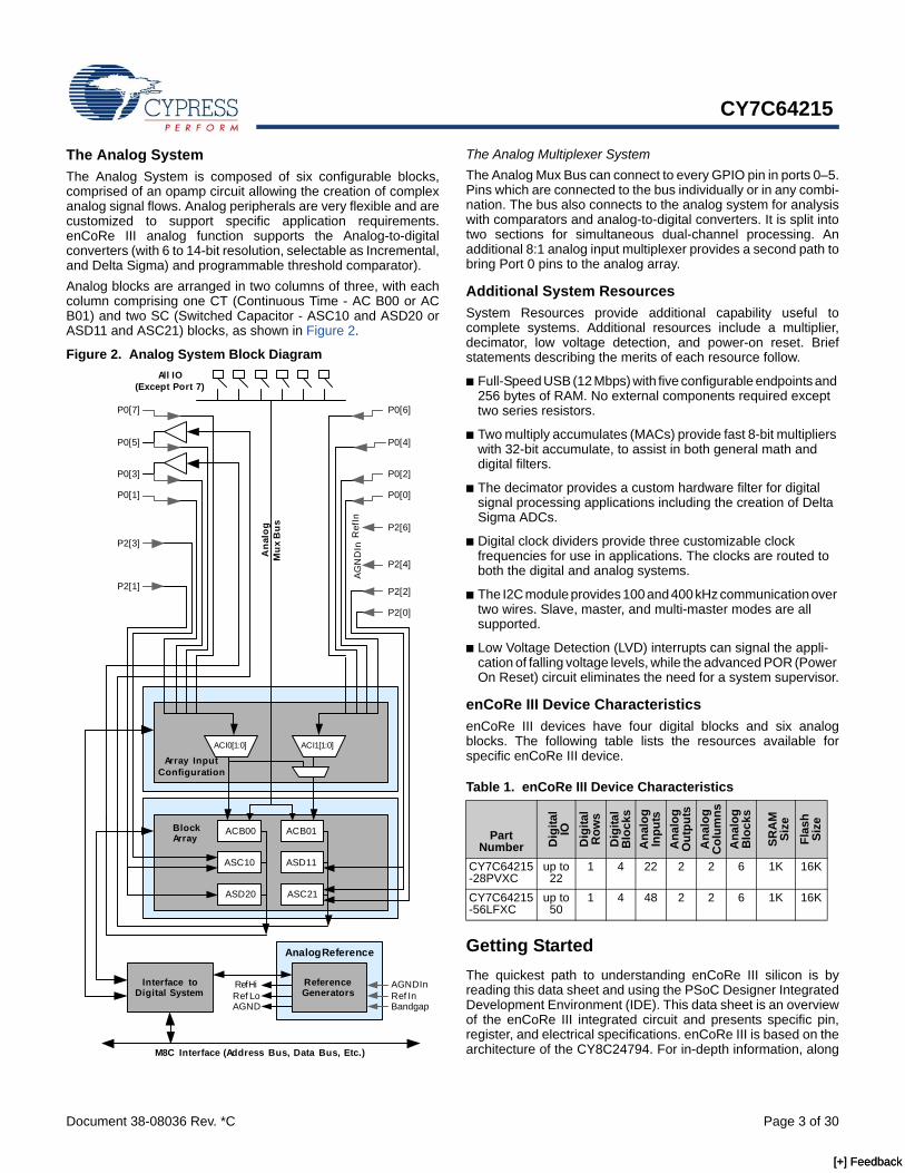
The Analog SystemThe Analog System is composed of six configurable blocks,comprised of an opamp circuit allowing the creation of complexanalog signal flows. Analog peripherals are very flexible and arecustomized to support specific application requirements.enCoRe III analog function supports the Analog-to-digitalconverters (with 6 to 14-bit resolution, selectable as Incremental,and Delta Sigma) and programmable threshold comparator).Analog blocks are arranged in two columns of three, with eachcolumn comprising one CT (Continuous Time - AC B00 or ACB01) and two SC (Switched Capacitor - ASC10 and ASD20 orASD11 and ASC21) blocks, as shown in Figure 2.
Figure 2. Analog System Block Diagram
The Analog Multiplexer SystemThe Analog Mux Bus can connect to every GPIO pin in ports 0–5.Pins which are connected to the bus individually or in any combi-nation. The bus also connects to the analog system for analysiswith comparators and analog-to-digital converters. It is split intotwo sections for simultaneous dual-channel processing. Anadditional 8:1 analog input multiplexer provides a second path tobring Port 0 pins to the analog array.
Additional System ResourcesSystem Resources provide additional capability useful tocomplete systems. Additional resources include a multiplier,decimator, low voltage detection, and power-on reset. Briefstatements describing the merits of each resource follow.
■ Full-Speed USB (12 Mbps) with five configurable endpoints and 256 bytes of RAM. No external components required except two series resistors.
■ Two multiply accumulates (MACs) provide fast 8-bit multipliers with 32-bit accumulate, to assist in both general math and digital filters.
■ The decimator provides a custom hardware filter for digital signal processing applications including the creation of Delta Sigma ADCs.
■ Digital clock dividers provide three customizable clock frequencies for use in applications. The clocks are routed to both the digital and analog systems.
■ The I2C module provides 100 and 400 kHz communication over two wires. Slave, master, and multi-master modes are all supported.
■ Low Voltage Detection (LVD) interrupts can signal the appli-cation of falling voltage levels, while the advanced POR (Power On Reset) circuit eliminates the need for a system supervisor.
enCoRe III Device CharacteristicsenCoRe III devices have four digital blocks and six analogblocks. The following table lists the resources available forspecific enCoRe III device.
Getting StartedThe quickest path to understanding enCoRe III silicon is byreading this data sheet and using the PSoC Designer IntegratedDevelopment Environment (IDE). This data sheet is an overviewof the enCoRe III integrated circuit and presents specific pin,register, and electrical specifications. enCoRe III is based on thearchitecture of the CY8C24794. For in-depth information, along
ACB00 ACB01BlockArray
Array InputConfiguration
ACI1[1:0]
ASD20
ACI0[1:0]
P0[6]
P0[4]
P0[2]
P0[0]
P2[2]
P2[0]
P2[6]
P2[4]
Ref
InA
GN
DIn
P0[7]
P0[5]
P0[3]
P0[1]
P2[3]
P2[1]
ReferenceGenerators
AGNDInRef InBandgap
RefHiRef LoAGND
ASD11
ASC21
ASC10
Interface toDigital System
M8C Interface (Address Bus, Data Bus, Etc.)
Analog Reference
All IO(Except Port 7)
Ana
log
Mux
Bus
Table 1. enCoRe III Device Characteristics
PartNumber D
igita
l IO
Dig
ital
Row
sD
igita
l B
lock
sA
nalo
g In
puts
Ana
log
Out
puts
Ana
log
Col
umns
Ana
log
Blo
cks
SRA
MSi
zeFl
ash
Size
CY7C64215-28PVXC
up to 22
1 4 22 2 2 6 1K 16K
CY7C64215-56LFXC
up to 50
1 4 48 2 2 6 1K 16K
[+] Feedback [+] Feedback
CY7C64215
Document 38-08036 Rev. *C Page 4 of 30
with detailed programming information, reference the PSoC™Mixed-Signal Array Technical Reference Manual.For up-to-date Ordering, Packaging, and Electrical Specificationinformation, reference the latest enCoRe III device data sheetson the web at http://www.cypress.com.
Development KitsDevelopment Kits are available from the following distributors:Digi-Key, Avnet, Arrow, and Future. The Cypress Online Storecontains development kits, C compilers, and all accessories forenCoRe III development. Go to the Cypress Online Store website at http://www.cypress.com, click the Online Store shoppingcart icon at the bottom of the web page, and click USB (UniversalSerial Bus) to view a current list of available items.
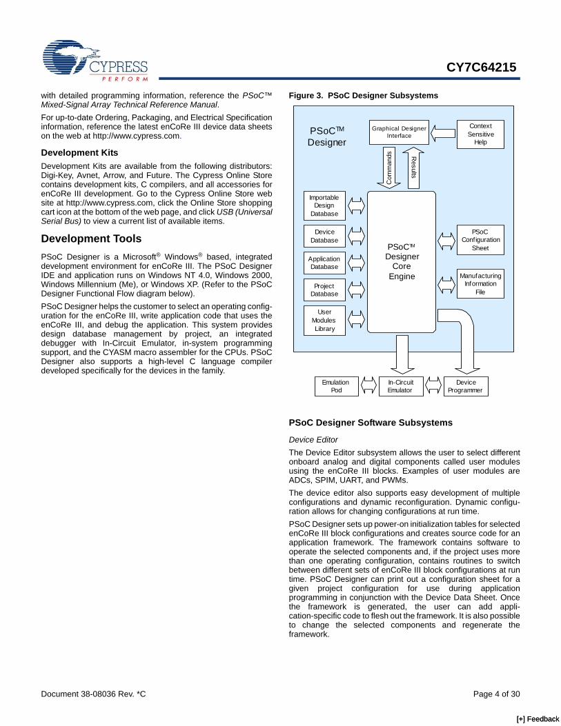
Development ToolsPSoC Designer is a Microsoft® Windows® based, integrateddevelopment environment for enCoRe III. The PSoC DesignerIDE and application runs on Windows NT 4.0, Windows 2000,Windows Millennium (Me), or Windows XP. (Refer to the PSoCDesigner Functional Flow diagram below).PSoC Designer helps the customer to select an operating config-uration for the enCoRe III, write application code that uses theenCoRe III, and debug the application. This system providesdesign database management by project, an integrateddebugger with In-Circuit Emulator, in-system programmingsupport, and the CYASM macro assembler for the CPUs. PSoCDesigner also supports a high-level C language compilerdeveloped specifically for the devices in the family.
Figure 3. PSoC Designer Subsystems
PSoC Designer Software Subsystems
Device EditorThe Device Editor subsystem allows the user to select differentonboard analog and digital components called user modulesusing the enCoRe III blocks. Examples of user modules areADCs, SPIM, UART, and PWMs.The device editor also supports easy development of multipleconfigurations and dynamic reconfiguration. Dynamic configu-ration allows for changing configurations at run time.PSoC Designer sets up power-on initialization tables for selectedenCoRe III block configurations and creates source code for anapplication framework. The framework contains software tooperate the selected components and, if the project uses morethan one operating configuration, contains routines to switchbetween different sets of enCoRe III block configurations at runtime. PSoC Designer can print out a configuration sheet for agiven project configuration for use during applicationprogramming in conjunction with the Device Data Sheet. Oncethe framework is generated, the user can add appli-cation-specific code to flesh out the framework. It is also possibleto change the selected components and regenerate theframework.
Com
man
ds Results
PSoCTM
DesignerCore
Engine
PSoCConfiguration
Sheet
ManufacturingInformation
File
DeviceDatabase
ImportableDesign
Database
DeviceProgrammer
Graphical DesignerInterface
ContextSensitive
Help
EmulationPod
In-CircuitEmulator
ProjectDatabase
ApplicationDatabase
UserModulesLibrary
PSoCTM
Designer
[+] Feedback [+] Feedback
CY7C64215
Document 38-08036 Rev. *C Page 5 of 30
Application EditorIn the Application Editor you can edit your C language andAssembly language source code. You can also assemble,compile, link, and build.
Assembler. The macro assembler allows the assembly code tomerge seamlessly with C code. The link libraries automaticallyuse absolute addressing or is compiled in relative mode, andlinked with other software modules to get absolute addressing.
C Language Compiler. A C language compiler is available thatsupports the enCoRe III family of devices. Even if you have neverworked in the C language before, the product quickly allows youto create complete C programs for the enCoRe III devices.The embedded, optimizing C compiler provides all the featuresof C tailored to the enCoRe III architecture. It comes completewith embedded libraries providing port and bus operations,standard keypad and display support, and extended mathfunctionality.
DebuggerThe PSoC Designer Debugger subsystem provides hardwarein-circuit emulation, allowing the designer to test the program ina physical system while providing an internal view of the enCoReIII device. Debugger commands allow the designer to read andprogram and read and write data memory, read and write IOregisters, read and write CPU registers, set and clear break-points, and provide program run, halt, and step control. Thedebugger also allows the designer to create a trace buffer ofregisters and memory locations of interest.
Online Help SystemThe online help system displays online, context-sensitive helpfor the user. Designed for procedural and quick reference, eachfunctional subsystem has its own context-sensitive help. Thissystem also provides tutorials and links to FAQs and an OnlineSupport Forum to aid the designer in getting started.
Hardware Tools
In-Circuit EmulatorA low cost, high functionality ICE Cube is available for devel-opment support. This hardware has the capability to programsingle devices.The emulator consists of a base unit that connects to the PC byway of a USB port. The base unit is universal which operates withall enCoRe III devices.
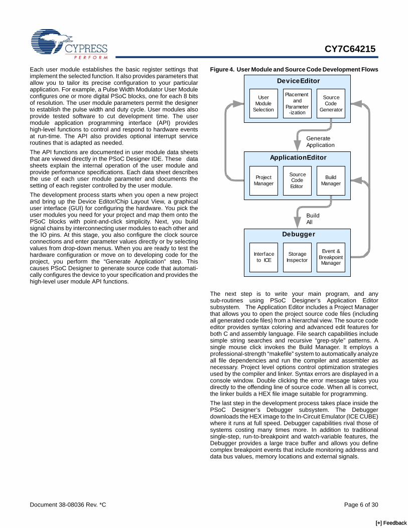
Designing with User ModulesThe development process for the enCoRe III device differs fromthat of a traditional fixed-function microprocessor. The config-urable analog and digital hardware blocks give the enCoRe IIIarchitecture a unique flexibility that pays dividends in managingspecification change during development and by loweringinventory costs. These configurable resources, called enCoReIII Blocks, have the ability to implement a wide variety ofuser-selectable functions. Each block has several registers thatdetermine its function and connectivity to other blocks, multi-plexers, buses and to the IO pins. Iterative development cyclespermit you to adapt the hardware and software. This substan-tially lowers the risk of having to select a different part to meetthe final design requirements.To speed the development process, the PSoC DesignerIntegrated Development Environment (IDE) provides a library ofpre-built, pre-tested hardware peripheral functions, called “UserModules.” User modules make selecting and implementingperipheral devices simple, and come in analog, digital, andmixed signal varieties.The user module library contains the following digital and analogmodule designs:
■ Analog Blocks❐ Incremental ADC (ADCINC)❐ Delta Sigma ADC (DelSig)❐ Programmable Threshold Comparator (CMPPRG)
■ Digital Blocks❐ Counters: 8-bit and 16-bit (Counter8 and Counter 16)❐ PWMs: 8-bit and 16-bit (PWM8 and PWM16)❐ Timers: 8-bit and 16-bit (Timer8 and Timer 16)❐ I2C Master (I2Cm)❐ SPI Master (SPIM)❐ SPI Slave (SPIS)❐ Full Duplex UART (UART)❐ RF (CYFISNP and CYFISPI)
■ System Resources❐ Protocols:
• USBFS• I2C Bootheader (Boothdr I2C)• USB Bootheader (BoothdrUSBFS)• USBUART
❐ Digital System Resources• E2PROM• LCD• LED• 7-segment LED (LED7SEG)• Shadow Registers (SHADOWREG)• Sleep Timer
[+] Feedback [+] Feedback
CY7C64215
Document 38-08036 Rev. *C Page 6 of 30
Each user module establishes the basic register settings thatimplement the selected function. It also provides parameters thatallow you to tailor its precise configuration to your particularapplication. For example, a Pulse Width Modulator User Moduleconfigures one or more digital PSoC blocks, one for each 8 bitsof resolution. The user module parameters permit the designerto establish the pulse width and duty cycle. User modules alsoprovide tested software to cut development time. The usermodule application programming interface (API) provideshigh-level functions to control and respond to hardware eventsat run-time. The API also provides optional interrupt serviceroutines that is adapted as needed.The API functions are documented in user module data sheetsthat are viewed directly in the PSoC Designer IDE. These datasheets explain the internal operation of the user module andprovide performance specifications. Each data sheet describesthe use of each user module parameter and documents thesetting of each register controlled by the user module. The development process starts when you open a new projectand bring up the Device Editor/Chip Layout View, a graphicaluser interface (GUI) for configuring the hardware. You pick theuser modules you need for your project and map them onto thePSoC blocks with point-and-click simplicity. Next, you buildsignal chains by interconnecting user modules to each other andthe IO pins. At this stage, you also configure the clock sourceconnections and enter parameter values directly or by selectingvalues from drop-down menus. When you are ready to test thehardware configuration or move on to developing code for theproject, you perform the “Generate Application” step. Thiscauses PSoC Designer to generate source code that automati-cally configures the device to your specification and provides thehigh-level user module API functions.
Figure 4. User Module and Source Code Development Flows
The next step is to write your main program, and anysub-routines using PSoC Designer’s Application Editorsubsystem. The Application Editor includes a Project Managerthat allows you to open the project source code files (includingall generated code files) from a hierarchal view. The source codeeditor provides syntax coloring and advanced edit features forboth C and assembly language. File search capabilities includesimple string searches and recursive “grep-style” patterns. Asingle mouse click invokes the Build Manager. It employs aprofessional-strength “makefile” system to automatically analyzeall file dependencies and run the compiler and assembler asnecessary. Project level options control optimization strategiesused by the compiler and linker. Syntax errors are displayed in aconsole window. Double clicking the error message takes youdirectly to the offending line of source code. When all is correct,the linker builds a HEX file image suitable for programming.The last step in the development process takes place inside thePSoC Designer’s Debugger subsystem. The Debuggerdownloads the HEX image to the In-Circuit Emulator (ICE CUBE)where it runs at full speed. Debugger capabilities rival those ofsystems costing many times more. In addition to traditionalsingle-step, run-to-breakpoint and watch-variable features, theDebugger provides a large trace buffer and allows you definecomplex breakpoint events that include monitoring address anddata bus values, memory locations and external signals.
Debugger
Interfaceto ICE
Application Editor
Device Editor
ProjectManager
SourceCodeEditor
StorageInspector
UserModule
Selection
Placementand
Parameter-ization
GenerateApplication
BuildAll
Event &BreakpointManager
BuildManager
SourceCode
Generator
[+] Feedback [+] Feedback
CY7C64215
Document 38-08036 Rev. *C Page 7 of 30
Document ConventionsAcronyms UsedThe following table lists the acronyms that are used in thisdocument.
Units of MeasureA units of measure table is located in the Electrical Specificationssection. Table 5 on page 13 lists all the abbreviations used tomeasure the enCoRe III devices.
Numeric NamingHexadecimal numbers are represented with all letters inuppercase with an appended lowercase ‘h’ (for example, ‘14h’ or‘3Ah’). Hexadecimal numbers may also be represented by a ‘0x’prefix, the C coding convention. Binary numbers have anappended lowercase ‘b’ (For example, 01010100b’ or‘01000011b’). Numbers not indicated by an ‘h’ or ‘b’ are decimal.
Acronym DescriptionAC alternating currentADC analog-to-digital converterAPI application programming interfaceCPU central processing unitCT continuous timeECO external crystal oscillatorEEPROM electrically erasable programmable read-only
memoryFSR full scale rangeGPIO general purpose IOGUI graphical user interfaceHBM human body modelLSb least-significant bitLVD low voltage detectMSb most-significant bitPC program counterPLL phase-locked loopPOR power on resetPPOR precision power on resetPSoC Programmable System-on-Chip™PWM pulse width modulatorSC switched capacitorSRAM static random access memoryICE in-circuit emulatorILO internal low speed oscillatorIMO internal main oscillatorIO input/outputIPOR imprecise power on reset
[+] Feedback [+] Feedback
CY7C64215
Document 38-08036 Rev. *C Page 8 of 30
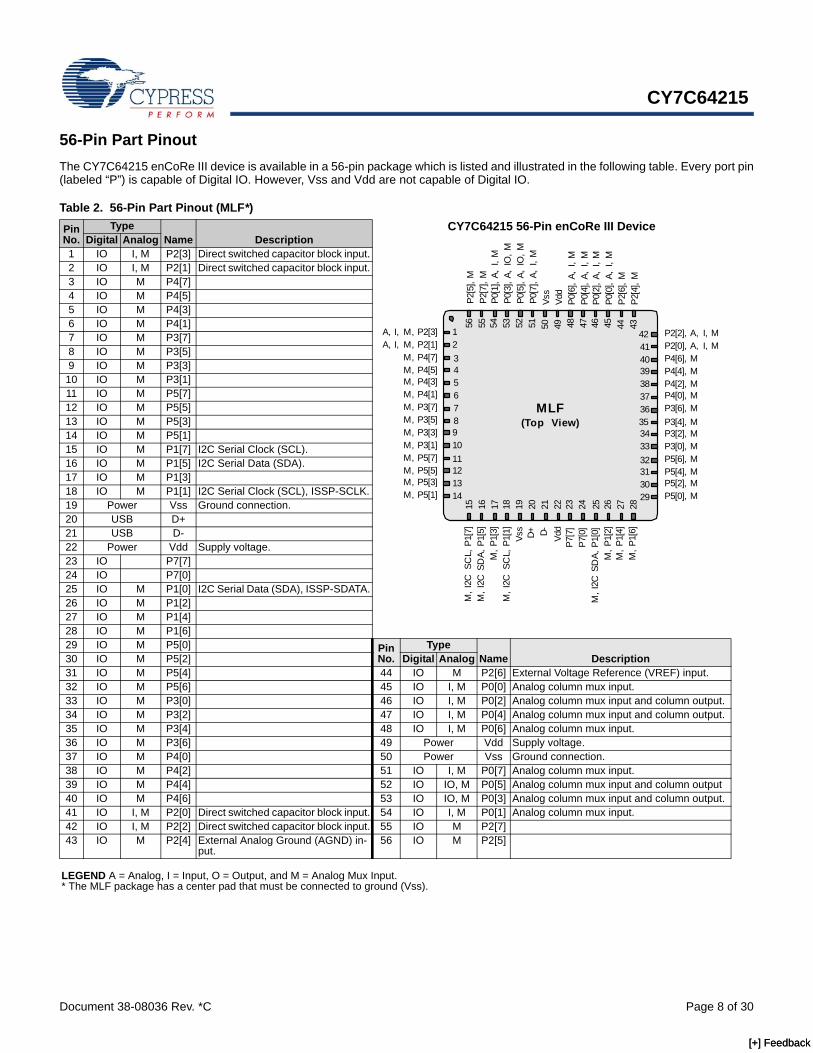
56-Pin Part PinoutThe CY7C64215 enCoRe III device is available in a 56-pin package which is listed and illustrated in the following table. Every port pin(labeled “P”) is capable of Digital IO. However, Vss and Vdd are not capable of Digital IO.
Table 2. 56-Pin Part Pinout (MLF*)
Pin No.
TypeName Description
CY7C64215 56-Pin enCoRe III DeviceDigital Analog
1 IO I, M P2[3] Direct switched capacitor block input.2 IO I, M P2[1] Direct switched capacitor block input.3 IO M P4[7]4 IO M P4[5]5 IO M P4[3]6 IO M P4[1]7 IO M P3[7]8 IO M P3[5]9 IO M P3[3]
10 IO M P3[1]11 IO M P5[7]12 IO M P5[5]13 IO M P5[3]14 IO M P5[1]15 IO M P1[7] I2C Serial Clock (SCL).16 IO M P1[5] I2C Serial Data (SDA).17 IO M P1[3]18 IO M P1[1] I2C Serial Clock (SCL), ISSP-SCLK.19 Power Vss Ground connection.20 USB D+21 USB D-22 Power Vdd Supply voltage.23 IO P7[7]24 IO P7[0]25 IO M P1[0] I2C Serial Data (SDA), ISSP-SDATA.26 IO M P1[2]27 IO M P1[4]28 IO M P1[6]29 IO M P5[0] Pin
No.Type
Name Description30 IO M P5[2] Digital Analog31 IO M P5[4] 44 IO M P2[6] External Voltage Reference (VREF) input.32 IO M P5[6] 45 IO I, M P0[0] Analog column mux input.33 IO M P3[0] 46 IO I, M P0[2] Analog column mux input and column output.34 IO M P3[2] 47 IO I, M P0[4] Analog column mux input and column output.35 IO M P3[4] 48 IO I, M P0[6] Analog column mux input.36 IO M P3[6] 49 Power Vdd Supply voltage.37 IO M P4[0] 50 Power Vss Ground connection.38 IO M P4[2] 51 IO I, M P0[7] Analog column mux input.39 IO M P4[4] 52 IO IO, M P0[5] Analog column mux input and column output 40 IO M P4[6] 53 IO IO, M P0[3] Analog column mux input and column output.41 IO I, M P2[0] Direct switched capacitor block input. 54 IO I, M P0[1] Analog column mux input.42 IO I, M P2[2] Direct switched capacitor block input. 55 IO M P2[7]43 IO M P2[4] External Analog Ground (AGND) in-
put.56 IO M P2[5]
LEGEND A = Analog, I = Input, O = Output, and M = Analog Mux Input. * The MLF package has a center pad that must be connected to ground (Vss).
MLF(Top View)
A, I, M, P2[3]A, I, M, P2[1]
M, P4[7]M, P4[5]M, P4[3]M, P4[1]M, P3[7]M, P3[5]M, P3[3]M, P3[1]M, P5[7]M, P5[5]M, P5[3]M, P5[1]
1234567891011121314
M, I
2C S
CL,
P1[
7]M
, I2C
SD
A, P
1[5]
M, P
1[3]
M, I
2C S
CL,
P1[
1]Vs
sD+ D- Vd
dP7
[7]
P7[0
]M
, I2C
SD
A, P
1[0]
M, P
1[2]
M, P
1[4]
M, P
1[6]
15 16 17 18 19 20 21 22 23 24 25 26 27 28P2
[4],
MP2
[6],
MP0
[0],
A, I
, MP0
[2],
A, I
, MP0
[4],
A, I
, MP0
[6],
A, I
, MVd
dVs
sP0
[7],
A, I
, MP0
[5],
A, I
O, M
P0[3
], A,
IO
, MP0
[1],
A, I
, MP2
[7],
MP2
[5],
M
4344454647484950515253545556
P2[2], A, I, MP2[0], A, I, MP4[6], MP4[4], MP4[2], MP4[0], MP3[6], MP3[4], MP3[2], MP3[0], MP5[6], MP5[4], MP5[2], MP5[0], M
4241403938373635343332313029
[+] Feedback [+] Feedback

CY7C64215
Document 38-08036 Rev. *C Page 9 of 30
28-Pin Part PinoutThe CY7C64215 enCoRe III device is available in a 28-pin package which is listed and illustrated in the following table. Every port pin(labeled with a “P”) is capable of Digital IO. However, Vss and Vdd are not capable of Digital IO.
Table 3. 28-Pin Part Pinout (SSOP)
Pin No.
TypeName Description
CY7C64215 28-Pin enCoRe III DeviceDigital Analog
1 Power GND Ground connection2 IO I, M P0[7] Analog column mux input.3 IO IO,M P0[5] Analog column mux input and column
output4 IO IO,M P0[3] Analog column mux input and column
output.5 IO I,M P0[1] Analog column mux input.6 IO M P2[5]7 IO M P2[3] Direct switched capacitor block input.8 IO M P2[1] Direct switched capacitor block input.9 IO M P1[7] I2C Serial Clock (SCL).
10 IO M P1[5] I2C Serial Data (SDA).11 IO M P1[3]12 IO M P1[1] I2C Serial Clock (SCL), ISSP-SCLK.13 Power GND Ground connection14 USB D+15 USB D-16 Power Vdd Supply voltage.17 IO M P1[0] I2C Serial Data (SDA), ISSP-SDATA.18 IO M P1[2]19 IO M P1[4]20 IO M P1[6]21 IO M P2[0] Direct switched capacitor block input.22 IO M P2[2] Direct switched capacitor block input.23 IO M P2[4] External Analog Ground (AGND) input.24 IO M P0[0] Analog column mux input.25 IO M P0[2] Analog column mux input and column
output.26 IO M P0[4] Analog column mux input and column
output.27 IO M P0[6] Analog column mux input.28 Power Vdd Supply voltage.
LEGEND A = Analog, I = Input, O = Output, and M = Analog Mux Input. * The MLF package has a center pad that must be connected to ground (Vss).
SSOP
123456789
1011121314
2827262524232221201918171615
VddP0[6], AIP0[4], AIP0[2], AIP0[0], AIP2[4]P2[2], AIP2[0], AIP1[6]P1[4]P1[2]P1[0], I2C SDAVddD-
VssAI, P0[7]
AIO, P0[5] AIO, P0[3]
AI, P0[1]P2[5]
AI, P2[3]AI, P2[1]
I2C SCL, P1[7]I2C SDA, P1[5]
P1[3]I2C SCL, P1[1]
VssD+
[+] Feedback [+] Feedback
CY7C64215
Document 38-08036 Rev. *C Page 10 of 30
Register ReferenceThe register conventions specific to this section are listed in the following table.
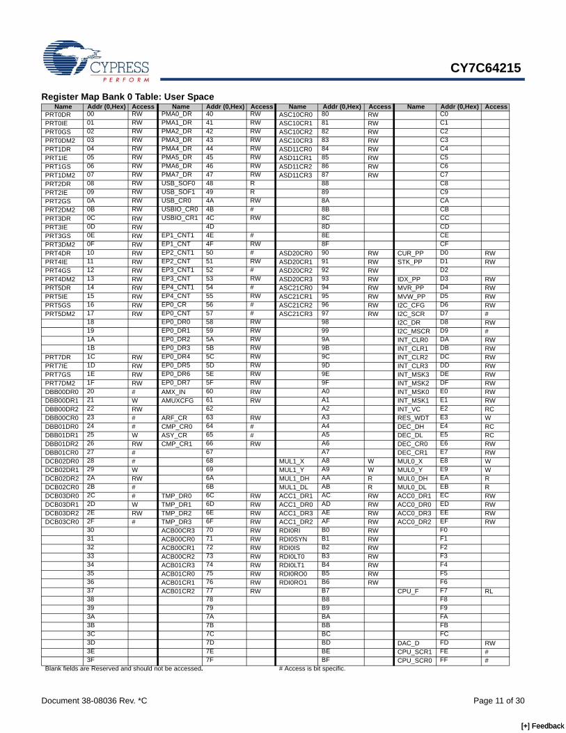
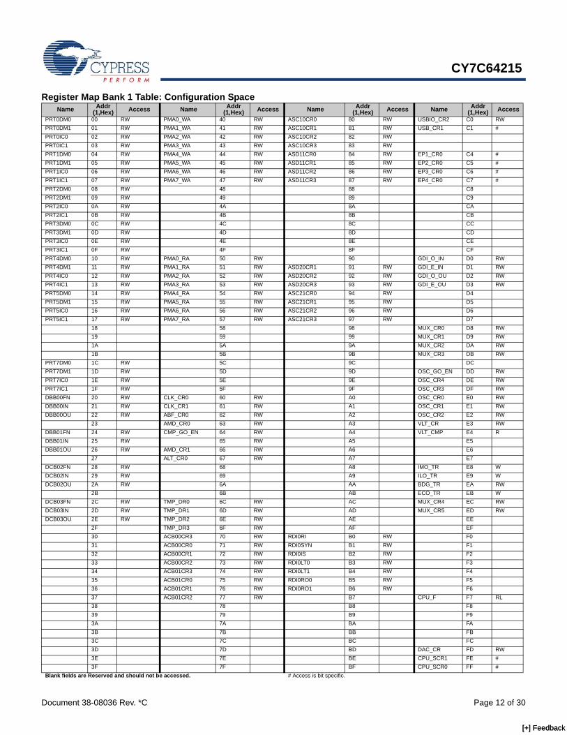
Register Mapping TablesThe enCoRe III device has a total register address space of 512bytes. The register space is referred to as IO space and isdivided into two banks. The XOI bit in the Flag register (CPU_F)determines which bank the user is currently in. When the XOI bitis set the user is in Bank 1.Note In the following register mapping tables, blank fields areReserved and should not be accessed.
Table 4. Register ConventionsConvention Description
R Read register or bit(s)W Write register or bit(s)L Logical register or bit(s)C Clearable register or bit(s)# Access is bit specific
[+] Feedback [+] Feedback
CY7C64215
Document 38-08036 Rev. *C Page 11 of 30
Register Map Bank 0 Table: User Space Name Addr (0,Hex) Access Name Addr (0,Hex) Access Name Addr (0,Hex) Access Name Addr (0,Hex) Access
PRT0DR 00 RW PMA0_DR 40 RW ASC10CR0 80 RW C0PRT0IE 01 RW PMA1_DR 41 RW ASC10CR1 81 RW C1PRT0GS 02 RW PMA2_DR 42 RW ASC10CR2 82 RW C2PRT0DM2 03 RW PMA3_DR 43 RW ASC10CR3 83 RW C3PRT1DR 04 RW PMA4_DR 44 RW ASD11CR0 84 RW C4PRT1IE 05 RW PMA5_DR 45 RW ASD11CR1 85 RW C5PRT1GS 06 RW PMA6_DR 46 RW ASD11CR2 86 RW C6PRT1DM2 07 RW PMA7_DR 47 RW ASD11CR3 87 RW C7PRT2DR 08 RW USB_SOF0 48 R 88 C8PRT2IE 09 RW USB_SOF1 49 R 89 C9PRT2GS 0A RW USB_CR0 4A RW 8A CAPRT2DM2 0B RW USBIO_CR0 4B # 8B CBPRT3DR 0C RW USBIO_CR1 4C RW 8C CCPRT3IE 0D RW 4D 8D CDPRT3GS 0E RW EP1_CNT1 4E # 8E CEPRT3DM2 0F RW EP1_CNT 4F RW 8F CFPRT4DR 10 RW EP2_CNT1 50 # ASD20CR0 90 RW CUR_PP D0 RWPRT4IE 11 RW EP2_CNT 51 RW ASD20CR1 91 RW STK_PP D1 RWPRT4GS 12 RW EP3_CNT1 52 # ASD20CR2 92 RW D2PRT4DM2 13 RW EP3_CNT 53 RW ASD20CR3 93 RW IDX_PP D3 RWPRT5DR 14 RW EP4_CNT1 54 # ASC21CR0 94 RW MVR_PP D4 RWPRT5IE 15 RW EP4_CNT 55 RW ASC21CR1 95 RW MVW_PP D5 RWPRT5GS 16 RW EP0_CR 56 # ASC21CR2 96 RW I2C_CFG D6 RWPRT5DM2 17 RW EP0_CNT 57 # ASC21CR3 97 RW I2C_SCR D7 #
18 EP0_DR0 58 RW 98 I2C_DR D8 RW19 EP0_DR1 59 RW 99 I2C_MSCR D9 #1A EP0_DR2 5A RW 9A INT_CLR0 DA RW1B EP0_DR3 5B RW 9B INT_CLR1 DB RW
PRT7DR 1C RW EP0_DR4 5C RW 9C INT_CLR2 DC RWPRT7IE 1D RW EP0_DR5 5D RW 9D INT_CLR3 DD RWPRT7GS 1E RW EP0_DR6 5E RW 9E INT_MSK3 DE RWPRT7DM2 1F RW EP0_DR7 5F RW 9F INT_MSK2 DF RWDBB00DR0 20 # AMX_IN 60 RW A0 INT_MSK0 E0 RWDBB00DR1 21 W AMUXCFG 61 RW A1 INT_MSK1 E1 RWDBB00DR2 22 RW 62 A2 INT_VC E2 RCDBB00CR0 23 # ARF_CR 63 RW A3 RES_WDT E3 WDBB01DR0 24 # CMP_CR0 64 # A4 DEC_DH E4 RCDBB01DR1 25 W ASY_CR 65 # A5 DEC_DL E5 RCDBB01DR2 26 RW CMP_CR1 66 RW A6 DEC_CR0 E6 RWDBB01CR0 27 # 67 A7 DEC_CR1 E7 RWDCB02DR0 28 # 68 MUL1_X A8 W MUL0_X E8 WDCB02DR1 29 W 69 MUL1_Y A9 W MUL0_Y E9 WDCB02DR2 2A RW 6A MUL1_DH AA R MUL0_DH EA RDCB02CR0 2B # 6B MUL1_DL AB R MUL0_DL EB RDCB03DR0 2C # TMP_DR0 6C RW ACC1_DR1 AC RW ACC0_DR1 EC RWDCB03DR1 2D W TMP_DR1 6D RW ACC1_DR0 AD RW ACC0_DR0 ED RWDCB03DR2 2E RW TMP_DR2 6E RW ACC1_DR3 AE RW ACC0_DR3 EE RWDCB03CR0 2F # TMP_DR3 6F RW ACC1_DR2 AF RW ACC0_DR2 EF RW
30 ACB00CR3 70 RW RDI0RI B0 RW F031 ACB00CR0 71 RW RDI0SYN B1 RW F132 ACB00CR1 72 RW RDI0IS B2 RW F233 ACB00CR2 73 RW RDI0LT0 B3 RW F334 ACB01CR3 74 RW RDI0LT1 B4 RW F435 ACB01CR0 75 RW RDI0RO0 B5 RW F536 ACB01CR1 76 RW RDI0RO1 B6 RW F637 ACB01CR2 77 RW B7 CPU_F F7 RL38 78 B8 F839 79 B9 F93A 7A BA FA3B 7B BB FB3C 7C BC FC3D 7D BD DAC_D FD RW3E 7E BE CPU_SCR1 FE #3F 7F BF CPU_SCR0 FF #
Blank fields are Reserved and should not be accessed. # Access is bit specific.
[+] Feedback [+] Feedback
CY7C64215
Document 38-08036 Rev. *C Page 12 of 30
Register Map Bank 1 Table: Configuration Space Name Addr
(1,Hex) Access Name Addr(1,Hex) Access Name Addr
(1,Hex) Access Name Addr(1,Hex) Access
PRT0DM0 00 RW PMA0_WA 40 RW ASC10CR0 80 RW USBIO_CR2 C0 RWPRT0DM1 01 RW PMA1_WA 41 RW ASC10CR1 81 RW USB_CR1 C1 #PRT0IC0 02 RW PMA2_WA 42 RW ASC10CR2 82 RWPRT0IC1 03 RW PMA3_WA 43 RW ASC10CR3 83 RWPRT1DM0 04 RW PMA4_WA 44 RW ASD11CR0 84 RW EP1_CR0 C4 #PRT1DM1 05 RW PMA5_WA 45 RW ASD11CR1 85 RW EP2_CR0 C5 #PRT1IC0 06 RW PMA6_WA 46 RW ASD11CR2 86 RW EP3_CR0 C6 #PRT1IC1 07 RW PMA7_WA 47 RW ASD11CR3 87 RW EP4_CR0 C7 #PRT2DM0 08 RW 48 88 C8PRT2DM1 09 RW 49 89 C9PRT2IC0 0A RW 4A 8A CAPRT2IC1 0B RW 4B 8B CBPRT3DM0 0C RW 4C 8C CCPRT3DM1 0D RW 4D 8D CDPRT3IC0 0E RW 4E 8E CEPRT3IC1 0F RW 4F 8F CFPRT4DM0 10 RW PMA0_RA 50 RW 90 GDI_O_IN D0 RWPRT4DM1 11 RW PMA1_RA 51 RW ASD20CR1 91 RW GDI_E_IN D1 RWPRT4IC0 12 RW PMA2_RA 52 RW ASD20CR2 92 RW GDI_O_OU D2 RWPRT4IC1 13 RW PMA3_RA 53 RW ASD20CR3 93 RW GDI_E_OU D3 RWPRT5DM0 14 RW PMA4_RA 54 RW ASC21CR0 94 RW D4PRT5DM1 15 RW PMA5_RA 55 RW ASC21CR1 95 RW D5PRT5IC0 16 RW PMA6_RA 56 RW ASC21CR2 96 RW D6PRT5IC1 17 RW PMA7_RA 57 RW ASC21CR3 97 RW D7
18 58 98 MUX_CR0 D8 RW19 59 99 MUX_CR1 D9 RW1A 5A 9A MUX_CR2 DA RW1B 5B 9B MUX_CR3 DB RW
PRT7DM0 1C RW 5C 9C DCPRT7DM1 1D RW 5D 9D OSC_GO_EN DD RWPRT7IC0 1E RW 5E 9E OSC_CR4 DE RWPRT7IC1 1F RW 5F 9F OSC_CR3 DF RWDBB00FN 20 RW CLK_CR0 60 RW A0 OSC_CR0 E0 RWDBB00IN 21 RW CLK_CR1 61 RW A1 OSC_CR1 E1 RWDBB00OU 22 RW ABF_CR0 62 RW A2 OSC_CR2 E2 RW
23 AMD_CR0 63 RW A3 VLT_CR E3 RWDBB01FN 24 RW CMP_GO_EN 64 RW A4 VLT_CMP E4 RDBB01IN 25 RW 65 RW A5 E5DBB01OU 26 RW AMD_CR1 66 RW A6 E6
27 ALT_CR0 67 RW A7 E7DCB02FN 28 RW 68 A8 IMO_TR E8 WDCB02IN 29 RW 69 A9 ILO_TR E9 WDCB02OU 2A RW 6A AA BDG_TR EA RW
2B 6B AB ECO_TR EB WDCB03FN 2C RW TMP_DR0 6C RW AC MUX_CR4 EC RWDCB03IN 2D RW TMP_DR1 6D RW AD MUX_CR5 ED RWDCB03OU 2E RW TMP_DR2 6E RW AE EE
2F TMP_DR3 6F RW AF EF30 ACB00CR3 70 RW RDI0RI B0 RW F031 ACB00CR0 71 RW RDI0SYN B1 RW F132 ACB00CR1 72 RW RDI0IS B2 RW F233 ACB00CR2 73 RW RDI0LT0 B3 RW F334 ACB01CR3 74 RW RDI0LT1 B4 RW F435 ACB01CR0 75 RW RDI0RO0 B5 RW F536 ACB01CR1 76 RW RDI0RO1 B6 RW F637 ACB01CR2 77 RW B7 CPU_F F7 RL38 78 B8 F839 79 B9 F93A 7A BA FA3B 7B BB FB3C 7C BC FC3D 7D BD DAC_CR FD RW3E 7E BE CPU_SCR1 FE #3F 7F BF CPU_SCR0 FF #
Blank fields are Reserved and should not be accessed. # Access is bit specific.
[+] Feedback [+] Feedback
CY7C64215
Document 38-08036 Rev. *C Page 13 of 30
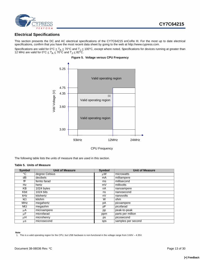
Electrical SpecificationsThis section presents the DC and AC electrical specifications of the CY7C64215 enCoRe III. For the most up to date electricalspecifications, confirm that you have the most recent data sheet by going to the web at http://www.cypress.com.Specifications are valid for 0°C < TA < 70°C and TJ < 100°C, except where noted. Specifications for devices running at greater than12 MHz are valid for 0°C < TA < 70°C and TJ < 82°C.
Figure 5. Voltage versus CPU Frequency
The following table lists the units of measure that are used in this section.
Table 5. Units of Measure
Symbol Unit of Measure Symbol Unit of Measure°C degree Celsius μW microwattsdB decibels mA milliamperefF femto farad ms millisecondHz hertz mV millivoltsKB 1024 bytes nA nanoampereKbit 1024 bits ns nanosecondkHz kilohertz nV nanovoltskΩ kilohm W ohm
MHz megahertz pA picoampereMΩ megaohm pF picofaradμA microampere pp peak-to-peakμF microfarad ppm parts per millionμH microhenry ps picosecondμs microsecond sps samples per second
CPU Frequency
Vdd
Vol
tage
(V)
5.25
4.35
3.60
3.00
4.75
93kHz 12MHz 24MHz
Valid operating region
Valid operating region
Valid operating region[1]
Note1. This is a valid operating region for the CPU, but USB hardware is non-functional in the voltage range from 3.60V – 4.35V.
[+] Feedback [+] Feedback
CY7C64215
Document 38-08036 Rev. *C Page 14 of 30
Absolute Maximum Ratings
Operating Temperature
μV microvolts s sigma: one standard deviationμVrms microvolts root-mean-square V volts
Table 5. Units of Measure (continued)
Symbol Unit of Measure Symbol Unit of Measure
Table 6. Absolute Maximum Ratings
Parameter Description Min Typ Max Unit NotesTSTG Storage Temperature –55 – +100 °C Higher storage temperatures
reduces data retention time.TA Ambient Temperature with Power Applied 0 – +70 °CVdd Supply Voltage on Vdd Relative to Vss –0.5 – +6.0 VVIO DC Input Voltage Vss – 0.5 – Vdd + 0.5 VVIO2 DC Voltage Applied to Tri-state Vss – 0.5 – Vdd + 0.5 VIMIO Maximum Current into any Port Pin –25 – +50 mAIMAIO Maximum Current into any Port Pin
Configured as Analog Driver–50 – +50 mA
ESD Electro Static Discharge Voltage 2000 – – V Human Body Model ESD.LU Latch Up Current – – 200 mA
Table 7. Operating Temperature
Parameter Description Min Typ Max Unit NotesTA Ambient Temperature 0 – +70 °CTJ Junction Temperature 0 – +88 °C The temperature rise from
ambient to junction is package specific. See “Thermal Impedance” on page 28. The user must limit the power consumption to comply with this requirement.
[+] Feedback [+] Feedback
CY7C64215
Document 38-08036 Rev. *C Page 15 of 30
DC Electrical Characteristics
DC Chip-Level SpecificationsThe following table lists guaranteed maximum and minimum specifications for the voltage and temperature ranges: 4.75V to 5.25Vand 0°C < TA < 70°C, or 3.0V to 3.6V and 0°C < TA < 70°C, respectively. Typical parameters apply to 5V and 3.3V at 25°C and arefor design guidance only.
DC General Purpose IO SpecificationsThe following table lists guaranteed maximum and minimum specifications for the voltage and temperature ranges: 4.75V to 5.25Vand 0°C < TA < 70°C, or 3.0V to 3.6V and 0°C < TA < 70°C, respectively. Typical parameters apply to 5V and 3.3V at 25°C and arefor design guidance only.
Table 8. DC Chip-Level Specifications
Parameter Description Min Typ Max Unit NotesVdd Supply Voltage 3.0 – 5.25 V See DC POR and LVD specifications, Table
16 on page 19. USB hardware is not functional when Vdd is between 3.6V - 4.35V.
IDD5 Supply Current, IMO = 24 MHz (5V) – 14 27 mA Conditions are Vdd = 5.0V, TA = 25°C, CPU = 3 MHz, SYSCLK doubler disabled, VC1 = 1.5 MHz, VC2 = 93.75 kHz, VC3 = 93.75 kHz, analog power = off.
IDD3 Supply Current, IMO = 24 MHz (3.3V) – 8 14 mA Conditions are Vdd = 3.3V, TA = 25°C, CPU = 3 MHz, SYSCLK doubler disabled, VC1 = 1.5 MHz, VC2 = 93.75 kHz, VC3 = 0.367 kHz, analog power = off.
ISB Sleep (Mode) Current with POR, LVD, Sleep Timer, and WDT.[2]
– 3 6.5 μA Conditions are with internal slow speed oscil-lator, Vdd = 3.3V, 0°C < TA < 55°C, analogpower = off.
ISBH Sleep (Mode) Current with POR, LVD, Sleep Timer, and WDT at high temperature.[2]
– 4 25 μA Conditions are with internal slow speed oscil-lator, Vdd = 3.3V, 55°C < TA < 70°C, analogpower = off.
Table 9. DC GPIO SpecificationsParameter Description Min Typ Max Unit NotesRPU Pull-Up Resistor 4 5.6 8 kΩRPD Pull-Down Resistor 4 5.6 8 kΩVOH High Output Level Vdd – 1.0 – – V IOH = 10 mA, Vdd = 4.75 to 5.25V (8 total loads, 4
on even port pins (for example, P0[2], P1[4]), 4 on odd port pins (for example, P0[3], P1[5])). 80 mA maximum combined IOH budget.
VOL Low Output Level – – 0.75 V IOL = 25 mA, Vdd = 4.75 to 5.25V (8 total loads, 4 on even port pins (for example, P0[2], P1[4]), 4 on odd port pins (for example, P0[3], P1[5])). 150 mA maximum combined IOL budget.
VIL Input Low Level – – 0.8 V Vdd = 3.0 to 5.25.VIH Input High Level 2.1 – V Vdd = 3.0 to 5.25.VH Input Hysteresis – 60 – mVIIL Input Leakage (Absolute Value) – 1 – nA Gross tested to 1 μA.CIN Capacitive Load on Pins as Input – 3.5 10 pF Package and pin dependent. Temp = 25°C.COUT Capacitive Load on Pins as Output – 3.5 10 pF Package and pin dependent. Temp = 25°C.
Note2. Standby current includes all functions (POR, LVD, WDT, Sleep Time) needed for reliable system operation. This should be compared with devices that have similar
functions enabled.
[+] Feedback [+] Feedback
CY7C64215
Document 38-08036 Rev. *C Page 16 of 30
DC Full-Speed USB SpecificationsThe following table lists guaranteed maximum and minimum specifications for the voltage and temperature ranges: 4.75V to 5.25Vand 0°C < TA < 70°C, or 3.0V to 3.6V and 0°C < TA < 70°C, respectively. Typical parameters apply to 5V and 3.3V at 25°C and arefor design guidance only.
DC Analog Output Buffer SpecificationsThe following tables list guaranteed maximum and minimum specifications for the voltage and temperature ranges: 4.75V to 5.25Vand 0°C < TA < 70°C, or 3.0V to 3.6V and 0°C < TA < 70°C, respectively. Typical parameters apply to 5V and 3.3V at 25°C and arefor design guidance only.
Table 10. DC Full-Speed (12 Mbps) USB SpecificationsParameter Description Min Typ Max Unit NotesUSB Interface
VDI Differential Input Sensitivity 0.2 – – V | (D+) – (D–) |VCM Differential Input Common Mode Range 0.8 – 2.5 VVSE Single Ended Receiver Threshold 0.8 – 2.0 VCIN Transceiver Capacitance – – 20 pFIIO High-Z State Data Line Leakage –10 – 10 μA 0V < VIN < 3.3V.REXT External USB Series Resistor 23 – 25 Ω In series with each USB pin.VUOH Static Output High, Driven 2.8 – 3.6 V 15 kΩ ± 5% to Ground. Internal pull-up
enabled.VUOHI Static Output High, Idle 2.7 – 3.6 V 15 kΩ ± 5% to Ground. Internal pull-up
enabled.VUOL Static Output Low – – 0.3 V 15 kΩ ± 5% to Ground. Internal pull-up
enabled.ZO USB Driver Output Impedance 28 – 44 Ω Including REXT Resistor.VCRS D+/D– Crossover Voltage 1.3 – 2.0 V
Table 11. 5V DC Analog Output Buffer Specifications
Parameter Description Min Typ Max Unit NotesVOSOB Input Offset Voltage (Absolute Value) – 3 12 mVTCVOSOB Average Input Offset Voltage Drift – +6 – μV/°CVCMOB Common-Mode Input Voltage Range 0.5 – Vdd - 1.0 VROUTOB Output Resistance
Power = LowPower = High
––
0.60.6
––
WW
VOHIGHOB High Output Voltage Swing (Load = 32 ohms to Vdd/2)Power = LowPower = High
0.5 x Vdd + 1.10.5 x Vdd + 1.1
––
––
VV
VOLOWOB Low Output Voltage Swing (Load = 32 ohms to Vdd/2)Power = LowPower = High
––
––
0.5 x Vdd – 1.30.5 x Vdd – 1.3
VV
ISOB Supply Current Including Bias Cell (No Load)Power = LowPower = High
––
1.12.6
5.18.8
mAmA
PSRROB Supply Voltage Rejection Ratio 53 64 – dB (0.5 x Vdd – 1.3) < VOUT < (Vdd – 2.3).
[+] Feedback [+] Feedback

CY7C64215
Document 38-08036 Rev. *C Page 17 of 30
DC Analog Reference SpecificationsThe following tables list guaranteed maximum and minimum specifications for the voltage and temperature ranges: 4.75V to 5.25Vand 0°C < TA < 70°C, or 3.0V to 3.6V and 0°C < TA < 70°C, respectively. Typical parameters apply to 5V and 3.3V at 25°C and arefor design guidance only.
Table 12. 3.3V DC Analog Output Buffer Specifications
Parameter Description Min Typ Max Unit NotesVOSOB Input Offset Voltage (Absolute Value) – 3 12 mVTCVOSOB Average Input Offset Voltage Drift – +6 – μV/°CVCMOB Common-Mode Input Voltage Range 0.5 - Vdd - 1.0 VROUTOB Output Resistance
Power = LowPower = High
––
11
––
WW
VOHIGHOB High Output Voltage Swing (Load = 1K ohms to Vdd/2)Power = LowPower = High
0.5 x Vdd + 1.00.5 x Vdd + 1.0
––
––
VV
VOLOWOB Low Output Voltage Swing (Load = 1K ohms to Vdd/2)Power = LowPower = High
––
––
0.5 x Vdd – 1.00.5 x Vdd – 1.0
VV
ISOB Supply Current Including Bias Cell (No Load)Power = LowPower = High –
0.82.0
2.04.3
mAmA
PSRROB Supply Voltage Rejection Ratio 34 64 – dB (0.5 x Vdd – 1.0) < VOUT < (0.5 x Vdd + 0.9).
Table 13. 5V DC Analog Reference Specifications
Parameter Description Min Typ Max UnitBG Bandgap Voltage Reference 1.28 1.30 1.32 V– AGND = Vdd/2[3] Vdd/2 – 0.04 Vdd/2 – 0.01 Vdd/2 + 0.007 V– AGND = 2 x BandGap[3] 2 x BG – 0.048 2 x BG – 0.030 2 x BG + 0.024 V– AGND = P2[4] (P2[4] = Vdd/2)[3] P2[4] – 0.011 P2[4] P2[4] + 0.011 V– AGND = BandGap[3] BG – 0.009 BG + 0.008 BG + 0.016 V– AGND = 1.6 x BandGap[3] 1.6 x BG – 0.022 1.6 x BG – 0.010 1.6 x BG + 0.018 V– AGND Block to Block Variation
(AGND = Vdd/2)[3]–0.034 0.000 0.034 V
– RefHi = Vdd/2 + BandGap Vdd/2 + BG – 0.10 Vdd/2 + BG Vdd/2 + BG + 0.10 V– RefHi = 3 x BandGap 3 x BG – 0.06 3 x BG 3 x BG + 0.06 V– RefHi = 2 x BandGap + P2[6] (P2[6] = 1.3V) 2 x BG + P2[6] – 0.113 2 x BG + P2[6] – 0.018 2 x BG + P2[6] + 0.077 V– RefHi = P2[4] + BandGap (P2[4] = Vdd/2) P2[4] + BG – 0.130 P2[4] + BG – 0.016 P2[4] + BG + 0.098 V– RefHi = P2[4] + P2[6] (P2[4] = Vdd/2, P2[6]
= 1.3V)P2[4] + P2[6] – 0.133 P2[4] + P2[6] – 0.016 P2[4] + P2[6]+ 0.100 V
– RefHi = 3.2 x BandGap 3.2 x BG – 0.112 3.2 x BG 3.2 x BG + 0.076 V– RefLo = Vdd/2 – BandGap Vdd/2 – BG – 0.04 Vdd/2 – BG + 0.024 Vdd/2 – BG + 0.04 V– RefLo = BandGap BG – 0.06 BG BG + 0.06 V– RefLo = 2 x BandGap – P2[6] (P2[6] = 1.3V) 2 x BG – P2[6] – 0.084 2 x BG – P2[6] + 0.025 2 x BG – P2[6] + 0.134 V– RefLo = P2[4] – BandGap (P2[4] = Vdd/2) P2[4] – BG – 0.056 P2[4] – BG + 0.026 P2[4] – BG + 0.107 V– RefLo = P2[4]-P2[6] (P2[4] = Vdd/2, P2[6] =
1.3V)P2[4] – P2[6] – 0.057 P2[4] – P2[6] + 0.026 P2[4] – P2[6] + 0.110 V
Note3. AGND tolerance includes the offsets of the local buffer in the enCoRe III block. Bandgap voltage is 1.3V ± 0.02V.
[+] Feedback [+] Feedback
CY7C64215
Document 38-08036 Rev. *C Page 18 of 30
DC Analog enCoRe III Block SpecificationsThe following table lists guaranteed maximum and minimum specifications for the voltage and temperature ranges: 4.75V to 5.25Vand 0°C < TA < 70°C, or 3.0V to 3.6V and 0°C < TA < 70°C, respectively. Typical parameters apply to 5V and 3.3V at 25°C and arefor design guidance only.
Table 14. 3.3V DC Analog Reference Specifications
Parameter Description Min Typ Max UnitBG Bandgap Voltage Reference 1.28 1.30 1.32 V– AGND = Vdd/2[3] Vdd/2 – 0.03 Vdd/2 – 0.01 Vdd/2 + 0.005 V– AGND = 2 x BandGap[3] Not Allowed– AGND = P2[4] (P2[4] = Vdd/2) P2[4] – 0.008 P2[4] + 0.001 P2[4] + 0.009 V– AGND = BandGap[3] BG – 0.009 BG + 0.005 BG + 0.015 V– AGND = 1.6 x BandGap[3] 1.6 x BG – 0.027 1.6 x BG – 0.010 1.6 x BG + 0.018 V– AGND Column to Column Variation (AGND =
Vdd/2)[3]–0.034 0.000 0.034 V
– RefHi = Vdd/2 + BandGap Not Allowed– RefHi = 3 x BandGap Not Allowed– RefHi = 2 x BandGap + P2[6] (P2[6] = 0.5V) Not Allowed– RefHi = P2[4] + BandGap (P2[4] = Vdd/2) Not Allowed– RefHi = P2[4] + P2[6] (P2[4] = Vdd/2, P2[6] = 0.5V) P2[4] + P2[6] – 0.075 P2[4] + P2[6] – 0.009 P2[4] + P2[6] + 0.057 V– RefHi = 3.2 x BandGap Not Allowed– RefLo = Vdd/2 – BandGap Not Allowed– RefLo = BandGap Not Allowed– RefLo = 2 x BandGap - P2[6] (P2[6] = 0.5V) Not Allowed– RefLo = P2[4] – BandGap (P2[4] = Vdd/2) Not Allowed– RefLo = P2[4]-P2[6] (P2[4] = Vdd/2, P2[6] = 0.5V) P2[4] – P2[6] – 0.048 P2[4] – P2[6] + 0.022 P2[4] – P2[6] + 0.092 V
Table 15. DC Analog enCoRe III Block Specifications
Parameter Description Min Typ Max Unit NotesRCT Resistor Unit Value (Continuous Time) – 12.2 – kΩCSC Capacitor Unit Value (Switched Capacitor) – 80 – fF
[+] Feedback [+] Feedback
CY7C64215
Document 38-08036 Rev. *C Page 19 of 30
DC POR and LVD SpecificationsThe following table lists guaranteed maximum and minimum specifications for the voltage and temperature ranges: 4.75V to 5.25Vand 0°C < TA < 70°C, or 3.0V to 3.6V and 0°C < TA < 70°C, respectively. Typical parameters apply to 5V or 3.3V at 25°C and are fordesign guidance only.Note The bits PORLEV and VM in the table below refer to bits in the VLT_CR register. See the PSoC Mixed-Signal Array TechnicalReference Manual for more information on the VLT_CR register.
Table 16. DC POR and LVD SpecificationsParameter Description Min Typ Max Unit Notes
VPPOR0RVPPOR1RVPPOR2R
Vdd Value for PPOR Trip (positive ramp)PORLEV[1:0] = 00bPORLEV[1:0] = 01bPORLEV[1:0] = 10b
–2.914.394.55
–VVV
VPPOR0VPPOR1VPPOR2
Vdd Value for PPOR Trip (negative ramp)PORLEV[1:0] = 00bPORLEV[1:0] = 01bPORLEV[1:0] = 10b
–2.824.394.55
–VVV
VPH0VPH1VPH2
PPOR HysteresisPORLEV[1:0] = 00bPORLEV[1:0] = 01bPORLEV[1:0] = 10b
–––
9200
–––
mVmVmV
VLVD0VLVD1VLVD2VLVD3VLVD4VLVD5VLVD6VLVD7
Vdd Value for LVD TripVM[2:0] = 000bVM[2:0] = 001bVM[2:0] = 010bVM[2:0] = 011bVM[2:0] = 100bVM[2:0] = 101bVM[2:0] = 110bVM[2:0] = 111b
2.862.963.073.924.394.554.634.72
2.923.023.134.004.484.644.734.81
2.98[4]
3.083.204.084.57
4.74[5]
4.824.91
V
VVVVVVV
Notes4. Always greater than 50 mV above PPOR (PORLEV = 00) for falling supply5. Always greater than 50 mV above PPOR (PORLEV = 10) for falling supply
[+] Feedback [+] Feedback
CY7C64215
Document 38-08036 Rev. *C Page 20 of 30
DC Programming SpecificationsThe following table lists guaranteed maximum and minimum specifications for the voltage and temperature ranges: 4.75V to 5.25Vand 0°C < TA < 70°C, or 3.0V to 3.6V and 0°C < TA < 70°C, respectively. Typical parameters apply to 5V and 3.3V at 25°C and arefor design guidance only.
Table 17. DC Programming Specifications
Parameter Description Min Typ Max Unit NotesIDDP Supply Current During Programming or
Verify– 15 30 mA
VILP Input Low Voltage During Programming or Verify
– – 0.8 V
VIHP Input High Voltage During Programming or Verify
2.1 – – V
IILP Input Current when Applying Vilp to P1[0] or P1[1] During Programming or Verify
– – 0.2 mA Driving internal pull-down resistor.
IIHP Input Current when Applying Vihp to P1[0] or P1[1] During Programming or Verify
– – 1.5 mA Driving internal pull-down resistor.
VOLV Output Low Voltage During Programming or Verify
– – Vss + 0.75 V
VOHV Output High Voltage During Programming or Verify
Vdd – 1.0 – Vdd V
FlashENPB Flash Endurance (per block) 50,000 – – – Erase/write cycles per block.FlashENT Flash Endurance (total)[6] 1,800,000 – – – Erase/write cycles.FlashDR Flash Data Retention 10 – – Years
Note6. A maximum of 36 x 50,000 block endurance cycles is allowed. This may be balanced between operations on 36x1 blocks of 50,000 maximum cycles each,
36x2 blocks of 25,000 maximum cycles each, or 36x4 blocks of 12,500 maximum cycles each (to limit the total number of cycles to 36x50,000 and that no single block ever sees more than 50,000 cycles).For the full industrial range, the user must employ a temperature sensor user module (FlashTemp) and feed the result to the temperature argument before writing. Refer to the Flash APIs Application Note AN2015 at http://www.cypress.com under Application Notes for more information.
[+] Feedback [+] Feedback
CY7C64215
Document 38-08036 Rev. *C Page 21 of 30
AC Electrical Characteristics
AC Chip-Level SpecificationsThe following table lists guaranteed maximum and minimum specifications for the voltage and temperature ranges: 4.75V to 5.25Vand 0°C < TA < 70°C, or 3.0V to 3.6V and 0°C < TA < 70°C, respectively. Typical parameters apply to 5V and 3.3V at 25°C and arefor design guidance only.
Figure 6. 24 MHz Period Jitter (IMO) Timing Diagram
Table 18. AC Chip-Level Specifications
Parameter Description Min Typ Max Unit NotesFIMO245V Internal Main Oscillator Frequency for 24 MHz
(5V)23.04 24 24.96[7, 8] MHz Trimmed for 5V operation using
factory trim values.FIMO243V Internal Main Oscillator Frequency for 24 MHz
(3.3V)22.08 24 25.92[7,9] MHz Trimmed for 3.3V operation
using factory trim values.FIMOUSB Internal Main Oscillator Frequency with USB
Frequency locking enabled and USB traffic present.
23.94 24 24.06[8] MHz 0°C < TA < 70°C
FCPU1 CPU Frequency (5V Nominal) 0.93 24 24.96[7,8] MHzFCPU2 CPU Frequency (3.3V Nominal) 0.93 12 12.96[8, 9] MHzFBLK5 Digital PSoC Block Frequency (5V Nominal) 0 48 49.92[7, 8,
10]MHz Refer to the AC Digital Block
Specifications.FBLK3 Digital PSoC Block Frequency (3.3V Nominal) 0 24 25.92[8, 10] MHzF32K1 Internal Low Speed Oscillator Frequency 15 32 64 kHzJitter32k 32 kHz Period Jitter – 100 nsStep24M 24 MHz Trim Step Size – 50 – kHzFout48M 48 MHz Output Frequency 46.08 48.0 49.92[7, 9] MHz Trimmed. Utilizing factory trim
values.Jitter24M1 24 MHz Period Jitter (IMO) Peak-to-Peak – 300 psFMAX Maximum frequency of signal on row input or
row output.– – 12.96 MHz
TRAMP Supply Ramp Time 0 – – μs
Jitter24M1
F24M
Notes7. 4.75V < Vdd < 5.25V.8. Accuracy derived from Internal Main Oscillator with appropriate trim for Vdd range.9. 3.0V < Vdd < 3.6V. See Application Note AN2012 “Adjusting PSoC Microcontroller Trims for Dual Voltage-Range Operation” for information on trimming for operation
at 3.3V.10. See the individual user module data sheets for information on maximum frequencies for user modules.
[+] Feedback [+] Feedback
CY7C64215
Document 38-08036 Rev. *C Page 22 of 30
AC General Purpose IO SpecificationsThe following table lists guaranteed maximum and minimum specifications for the voltage and temperature ranges: 4.75V to 5.25Vand 0°C < TA < 70°C, or 3.0V to 3.6V and 0°C < TA < 70°C, respectively. Typical parameters apply to 5V and 3.3V at 25°C and arefor design guidance only.
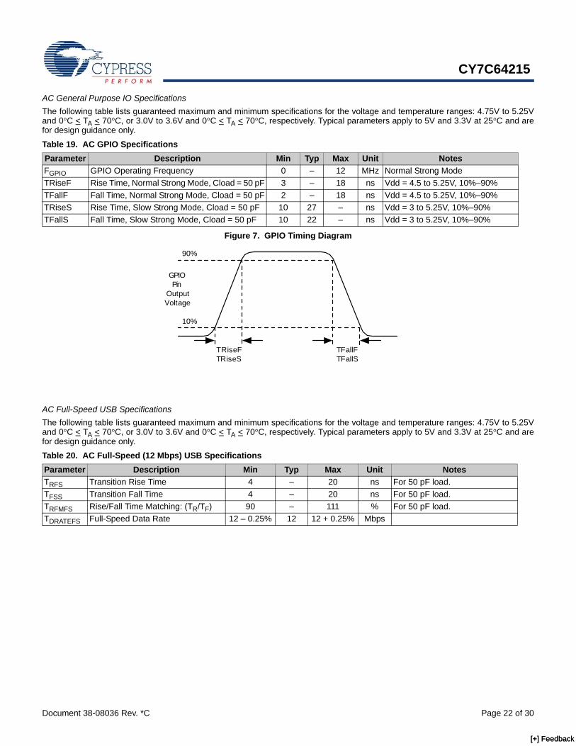
Figure 7. GPIO Timing Diagram
AC Full-Speed USB SpecificationsThe following table lists guaranteed maximum and minimum specifications for the voltage and temperature ranges: 4.75V to 5.25Vand 0°C < TA < 70°C, or 3.0V to 3.6V and 0°C < TA < 70°C, respectively. Typical parameters apply to 5V and 3.3V at 25°C and arefor design guidance only.
Table 19. AC GPIO SpecificationsParameter Description Min Typ Max Unit NotesFGPIO GPIO Operating Frequency 0 – 12 MHz Normal Strong ModeTRiseF Rise Time, Normal Strong Mode, Cload = 50 pF 3 – 18 ns Vdd = 4.5 to 5.25V, 10%–90%TFallF Fall Time, Normal Strong Mode, Cload = 50 pF 2 – 18 ns Vdd = 4.5 to 5.25V, 10%–90%TRiseS Rise Time, Slow Strong Mode, Cload = 50 pF 10 27 – ns Vdd = 3 to 5.25V, 10%–90%TFallS Fall Time, Slow Strong Mode, Cload = 50 pF 10 22 – ns Vdd = 3 to 5.25V, 10%–90%
Table 20. AC Full-Speed (12 Mbps) USB SpecificationsParameter Description Min Typ Max Unit NotesTRFS Transition Rise Time 4 – 20 ns For 50 pF load. TFSS Transition Fall Time 4 – 20 ns For 50 pF load. TRFMFS Rise/Fall Time Matching: (TR/TF) 90 – 111 % For 50 pF load. TDRATEFS Full-Speed Data Rate 12 – 0.25% 12 12 + 0.25% Mbps
TFallFTFallS
TRiseFTRiseS
90%
10%
GPIOPin
OutputVoltage
[+] Feedback [+] Feedback
CY7C64215
Document 38-08036 Rev. *C Page 23 of 30
AC Digital Block SpecificationsThe following table lists guaranteed maximum and minimum specifications for the voltage and temperature ranges: 4.75V to 5.25Vand 0°C < TA < 70°C, or 3.0V to 3.6V and 0°C < TA < 70°C, respectively. Typical parameters apply to 5V and 3.3V at 25°C and arefor design guidance only.
AC External Clock SpecificationsThe following tables list guaranteed maximum and minimum specifications for the voltage and temperature ranges: 4.75V to 5.25Vand 0°C < TA < 70°C, or 3.0V to 3.6V and 0°C < TA < 70°C, respectively. Typical parameters apply to 5V and 3.3V at 25°C and arefor design guidance only.
Table 21. AC Digital Block Specifications
Function Description Min Typ Max Unit NotesTimer Capture Pulse Width 50[11] – – ns
Maximum Frequency, No Capture – – 49.92 MHz 4.75V < Vdd < 5.25V.Maximum Frequency, With Capture – – 25.92 MHz
Counter Enable Pulse Width 50[11] – – nsMaximum Frequency, No Enable Input – – 49.92 MHz 4.75V < Vdd < 5.25V.Maximum Frequency, Enable Input – – 25.92 MHz
Dead Band
Kill Pulse Width:Asynchronous Restart Mode 20 – – nsSynchronous Restart Mode 50[11] – – nsDisable Mode 50[12] – – ns
Maximum Frequency – – 49.92 MHz 4.75V < Vdd < 5.25V.CRCPRS(PRS Mode)
Maximum Input Clock Frequency – – 49.92 MHz 4.75V < Vdd < 5.25V.
CRCPRS(CRC Mode)
Maximum Input Clock Frequency – – 24.6 MHz
SPIM Maximum Input Clock Frequency – – 8.2 MHz Maximum data rate at 4.1 MHz due to 2 x over clocking.
SPIS Maximum Input Clock Frequency – – 4.1 MHzWidth of SS_ Negated Between Trans-missions
50[11] – – ns
Trans-mitter
Maximum Input Clock Frequency – – 24.6 MHz Maximum data rate at 3.08 MHz due to 8 x over clocking.
Receiver Maximum Input Clock Frequency – – 24.6 MHz Maximum data rate at 3.08 MHz due to 8 x over clocking.
Table 22. AC External Clock Specifications
Parameter Description Min Typ Max Unit NotesFOSCEXT Frequency for USB Applications 23.94 24 24.06 MHz– Duty Cycle 47 50 53 %– Power - up to IMO Switch 150 – – μs
Note11. 50 ns minimum input pulse width is based on the input synchronizers running at 24 MHz (42 ns nominal period).
[+] Feedback [+] Feedback

CY7C64215
Document 38-08036 Rev. *C Page 24 of 30
AC Analog Output Buffer SpecificationsThe following tables list guaranteed maximum and minimum specifications for the voltage and temperature ranges: 4.75V to 5.25Vand 0°C < TA < 70°C, or 3.0V to 3.6V and 0°C < TA < 70°C, respectively. Typical parameters apply to 5V and 3.3V at 25°C and arefor design guidance only.
Table 23. 5V AC Analog Output Buffer Specifications
Parameter Description Min Typ Max Unit NotesTROB Rising Settling Time to 0.1%, 1V Step, 100 pF Load
Power = Low Power = High
––
––
2.52.5
μsμs
TSOB Falling Settling Time to 0.1%, 1V Step, 100 pF Load Power = Low Power = High
––
––
2.22.2
μsμs
SRROB Rising Slew Rate (20% to 80%), 1V Step, 100 pF Load Power = Low Power = High
0.650.65
––
––
V/μsV/μs
SRFOB Falling Slew Rate (80% to 20%), 1V Step, 100 pF Load Power = Low Power = High
0.650.65
––
––
V/μsV/μs
BWOBSS Small Signal Bandwidth, 20mVpp, 3-dB BW, 100 pF Load Power = Low Power = High
0.80.8
––
––
MHzMHz
BWOBLS Large Signal Bandwidth, 1Vpp, 3-dB BW, 100 pF Load Power = Low Power = High
300300
––
––
kHzkHz
Table 24. 3.3V AC Analog Output Buffer Specifications
Parameter Description Min Typ Max Unit NotesTROB Rising Settling Time to 0.1%, 1V Step, 100 pF Load
Power = Low Power = High
––
––
3.83.8
μsμs
TSOB Falling Settling Time to 0.1%, 1V Step, 100 pF Load Power = Low Power = High
––
––
2.62.6
μsμs
SRROB Rising Slew Rate (20% to 80%), 1V Step, 100 pF Load Power = Low Power = High
0.50.5
––
––
V/μsV/μs
SRFOB Falling Slew Rate (80% to 20%), 1V Step, 100 pF Load Power = Low Power = High
0.50.5
––
––
V/μsV/μs
BWOBSS Small Signal Bandwidth, 20mVpp, 3dB BW, 100 pF Load Power = Low Power = High
0.70.7
––
––
MHzMHz
BWOBLS Large Signal Bandwidth, 1Vpp, 3dB BW, 100 pF Load Power = Low Power = High
200200
––
––
kHzkHz
[+] Feedback [+] Feedback
CY7C64215
Document 38-08036 Rev. *C Page 25 of 30
AC Programming SpecificationsThe following table lists guaranteed maximum and minimum specifications for the voltage and temperature ranges: 4.75V to 5.25Vand 0°C < TA < 70°C, or 3.0V to 3.6V and 0°C < TA < 70°C, respectively. Typical parameters apply to 5V and 3.3V at 25°C and arefor design guidance only.
AC I2C SpecificationsThe following table lists guaranteed maximum and minimum specifications for the voltage and temperature ranges: 4.75V to 5.25Vand 0°C < TA < 70°C, or 3.0V to 3.6V and 0°C < TA < 70°C, respectively. Typical parameters apply to 5V and 3.3V at 25°C and arefor design guidance only.
Table 25. AC Programming SpecificationsParameter Description Min Typ Max Unit NotesTRSCLK Rise Time of SCLK 1 – 20 ns
TFSCLK Fall Time of SCLK 1 – 20 ns
TSSCLK Data Set up Time to Falling Edge of SCLK 40 – – ns
THSCLK Data Hold Time from Falling Edge of SCLK 40 – – ns
FSCLK Frequency of SCLK 0 – 8 MHz
TERASEB Flash Erase Time (Block) – 10 – ms
TWRITE Flash Block Write Time – 30 – ms
TDSCLK Data Out Delay from Falling Edge of SCLK – – 45 ns Vdd > 3.6
TDSCLK3 Data Out Delay from Falling Edge of SCLK – – 50 ns 3.0 < Vdd < 3.6
Table 26. AC Characteristics of the I2C SDA and SCL Pins for Vdd
Parameter DescriptionStandard Mode Fast Mode
Unit NotesMin Max Min Max
FSCLI2C SCL Clock Frequency 0 100 0 400 kHz
THDSTAI2C Hold Time (repeated) START Condition. After this period, the first clock pulse is generated.
4.0 – 0.6 – μs
TLOWI2C LOW Period of the SCL Clock 4.7 – 1.3 – μs
THIGHI2C HIGH Period of the SCL Clock 4.0 – 0.6 – μs
TSUSTAI2C Setup Time for a Repeated START Condition 4.7 – 0.6 – μs
THDDATI2C Data Hold Time 0 – 0 – μs
TSUDATI2C Data Setup Time 250 – 100[12] – ns
TSUSTOI2C Setup Time for STOP Condition 4.0 – 0.6 – μs
TBUFI2C Bus Free Time Between a STOP and START Condition
4.7 – 1.3 – μs
TSPI2C Pulse Width of spikes are suppressed by the input filter.
– – 0 50 ns
Note12. A Fast-Mode I2C-bus device can be used in a Standard-Mode I2C-bus system, but the requirement tSU;DAT Š 250 ns must then be met. This automatically
be the case if the device does not stretch the LOW period of the SCL signal. If such device does stretch the LOW period of the SCL signal, it must output the next data bit to the SDA line trmax + tSU;DAT = 1000 + 250 = 1250 ns (according to the Standard-Mode I2C-bus specification) before the SCL line is released.
[+] Feedback [+] Feedback
CY7C64215
Document 38-08036 Rev. *C Page 26 of 30
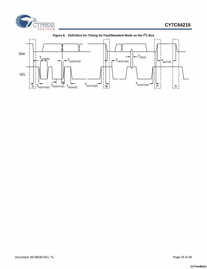
Figure 8. Definition for Timing for Fast/Standard Mode on the I2C Bus
SDA
SCL
S Sr SP
TBUFI2C
TSPI2CTHDSTAI2C
TSUSTOI2CTSUSTAI2C
TLOWI2C
THIGHI2CTHDDATI2CTHDSTAI2C
TSUDATI2C
[+] Feedback [+] Feedback
CY7C64215
Document 38-08036 Rev. *C Page 27 of 30
Packaging InformationThis section illustrates the package specification for the CY7C64215 enCoRe III, along with the thermal impedance for the package.Important Note Emulation tools may require a larger area on the target PCB than the chip’s footprint. For a detailed description ofthe emulation tools’ dimensions, refer to the document titled PSoC Emulator Pod Dimensions athttp://www.cypress.com/design/MR10161.
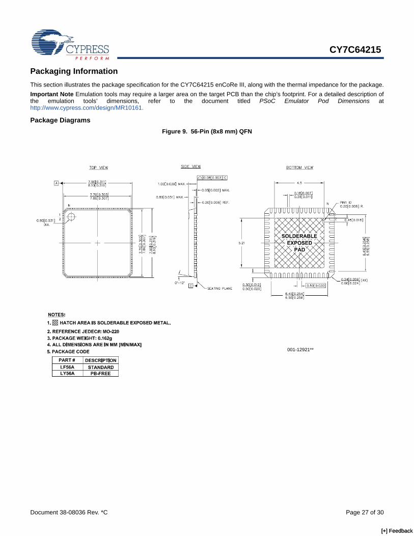
Package DiagramsFigure 9. 56-Pin (8x8 mm) QFN
001-12921**
[+] Feedback [+] Feedback
CY7C64215
Document 38-08036 Rev. *C Page 28 of 30
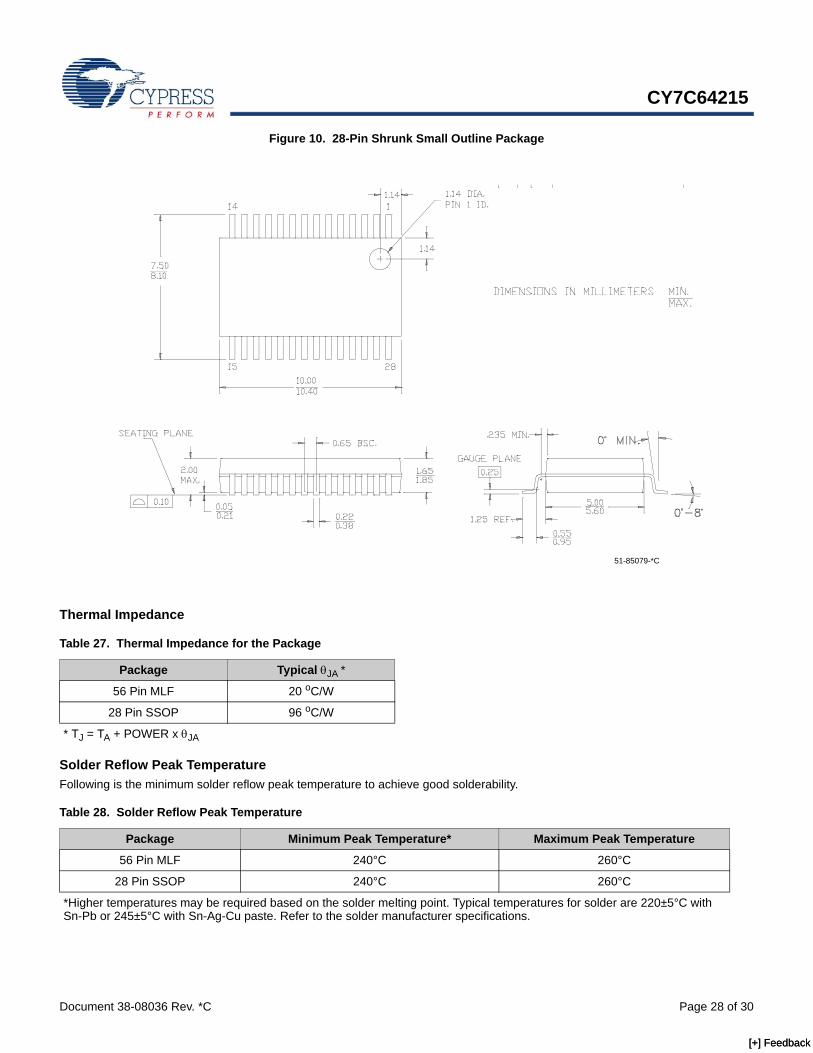
Figure 10. 28-Pin Shrunk Small Outline Package
Thermal Impedance
Solder Reflow Peak TemperatureFollowing is the minimum solder reflow peak temperature to achieve good solderability.
Table 27. Thermal Impedance for the Package
Package Typical θJA *
56 Pin MLF 20 oC/W
28 Pin SSOP 96 oC/W
* TJ = TA + POWER x θJA
51-85079-*C
Table 28. Solder Reflow Peak Temperature
Package Minimum Peak Temperature* Maximum Peak Temperature
56 Pin MLF 240°C 260°C
28 Pin SSOP 240°C 260°C
*Higher temperatures may be required based on the solder melting point. Typical temperatures for solder are 220±5°C with Sn-Pb or 245±5°C with Sn-Ag-Cu paste. Refer to the solder manufacturer specifications.
[+] Feedback [+] Feedback
CY7C64215
Document 38-08036 Rev. *C Page 29 of 30
Ordering Information
Package HandlingSome IC packages require baking before they are soldered onto a PCB to remove moisture that may have been absorbed after leavingthe factory. A label on the packaging has details about actual bake temperature and the minimum bake time to remove this moisture.The maximum bake time is the aggregate time that the parts are exposed to the bake temperature. Exceeding this exposure time maydegrade device reliability.
Parameter Description Min Typical Max UnitTBAKETEMP Bake Temperature 125 See package label °CTBAKETIME Bake Time See package label 72 hours
Package Ordering Code Flash Size SRAM (Bytes)56-Pin MLF CY7C64215-56LFXC 16K 1K
28-Pin SSOP CY7C64215-28PVXC 16K 1K
[+] Feedback [+] Feedback
Document 38-08036 Rev. *C Revised December 08, 2008 Page 30 of 30
enCoRe, PSoC, and Programmable System-on-Chip are trademarks of Cypress Semiconductor Corporation. Purchase of I2C components from Cypress or one of its sublicensed AssociatedCompanies conveys a license under the Philips I2C Patent Rights to use these components in an I2C system, provided that the system conforms to the I2C Standard Specification as defined by Philips.All products and company names mentioned in this document may be the trademarks of their respective holders.
CY7C64215
© Cypress Semiconductor Corporation, 2007-2008. The information contained herein is subject to change without notice. Cypress Semiconductor Corporation assumes no responsibility for the use ofany circuitry other than circuitry embodied in a Cypress product. Nor does it convey or imply any license under patent or other rights. Cypress products are not warranted nor intended to be used formedical, life support, life saving, critical control or safety applications, unless pursuant to an express written agreement with Cypress. Furthermore, Cypress does not authorize its products for use ascritical components in life-support systems where a malfunction or failure may reasonably be expected to result in significant injury to the user. The inclusion of Cypress products in life-support systemsapplication implies that the manufacturer assumes all risk of such use and in doing so indemnifies Cypress against all charges.
Any Source Code (software and/or firmware) is owned by Cypress Semiconductor Corporation (Cypress) and is protected by and subject to worldwide patent protection (United States and foreign),United States copyright laws and international treaty provisions. Cypress hereby grants to licensee a personal, non-exclusive, non-transferable license to copy, use, modify, create derivative works of,and compile the Cypress Source Code and derivative works for the sole purpose of creating custom software and or firmware in support of licensee product to be used only in conjunction with a Cypressintegrated circuit as specified in the applicable agreement. Any reproduction, modification, translation, compilation, or representation of this Source Code except as specified above is prohibited withoutthe express written permission of Cypress.
Disclaimer: CYPRESS MAKES NO WARRANTY OF ANY KIND, EXPRESS OR IMPLIED, WITH REGARD TO THIS MATERIAL, INCLUDING, BUT NOT LIMITED TO, THE IMPLIED WARRANTIESOF MERCHANTABILITY AND FITNESS FOR A PARTICULAR PURPOSE. Cypress reserves the right to make changes without further notice to the materials described herein. Cypress does notassume any liability arising out of the application or use of any product or circuit described herein. Cypress does not authorize its products for use as critical components in life-support systems wherea malfunction or failure may reasonably be expected to result in significant injury to the user. The inclusion of Cypress’ product in a life-support systems application implies that the manufacturerassumes all risk of such use and in doing so indemnifies Cypress against all charges.
Use may be limited by and subject to the applicable Cypress software license agreement.
Document History Page
Sales, Solutions, and Legal Information Worldwide Sales and Design SupportCypress maintains a worldwide network of offices, solution centers, manufacturer’s representatives, and distributors. To find the officeclosest to you, visit us at cypress.com/sales.
ProductsPSoC psoc.cypress.com
Clocks & Buffers clocks.cypress.com
Wireless wireless.cypress.com
Memories memory.cypress.com
Image Sensors image.cypress.com
PSoC SolutionsGeneral psoc.cypress.com/solutionsLow Power/Low Voltage psoc.cypress.com/low-powerPrecision Analog psoc.cypress.com/precision-analogLCD Drive psoc.cypress.com/lcd-driveCAN 2.0b psoc.cypress.com/canUSB psoc.cypress.com/usb
Description Title: CY7C64215, enCoRe™ III Full Speed USB ControllerDocument Number: 38-08036
Rev. ECN No. Submission Date
Orig. of Change Description of Change
** 131325 See ECN XGR New data sheet*A 385256 See ECN BHA Changed from Advance Information to Preliminary.
Added standard data sheet items.Changed Part number from CY7C642xx to CY7C64215.
*B 2547630 08/04/08 AZIEL/PYRS Operational voltage range for USB specified under "Full-Speed USB (12Mbps)". CMP_GO_EN1 register removed as it has no functionality on Radon.Figure "CPU Frequency" adjusted to show invalid operating region for USB with footnote describing reason.DC electrical characteristic, Vdd. Note added describing where USB hardware is non-functional.
*C 2620679 12/12/08 CMCC/PYRS Added Package Handling informationDeleted note regarding link to amkor.com for MLF package dimensions
[+] Feedback [+] Feedback