Embed Size (px)
Citation preview
12/05/14 CAS2014 ADCs & DACs 1
CERN Accelerator SchoolADCs and DACs
(Analogue to Digital and Digital to Analogue Converters)
John Pickering, Metron Designs Ltd, Norwich, UK
With grateful acknowledgment to John Pett (retired from CERN)
12/05/14 CAS2014 ADCs & DACs 2
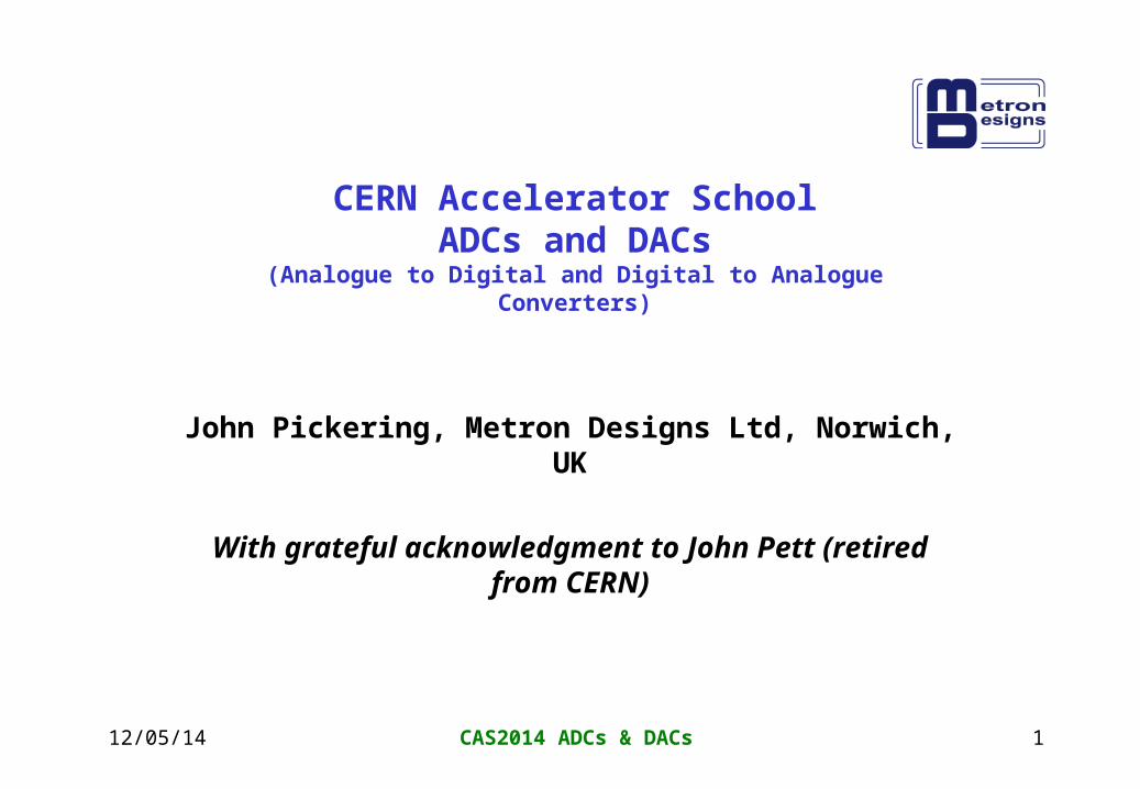
ADCs & DACs General Use
• Interface between Analogue & Digital environments• Trend is “Digital to the Antenna”• Most ADCs contain DACs in a feedback loop• Delta-Sigma ADCs use both ADCs and DACs in the loop
12/05/14 CAS2014 ADCs & DACs 3
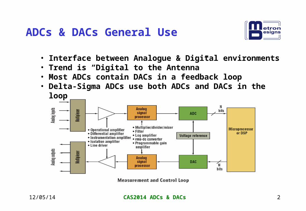
ADC DAC Subjects
• Terms, nomenclature, standards and specs.• Common ADC types
– Will mainly discuss DACs within ADC types– Flash– Pipeline– Successive Approximation Register (SAR)– Charge Balance, DVMs– Delta Sigma
• Applicability of types• Off the shelf “state of the art”• Some application problems & solutions• The future for accelerators?
12/05/14 CAS2014 ADCs & DACs 4
Terms, Nomenclature & Specs
• Many terms relate to AC measurement– Eg “SINAD”, “Over-sampling”– Standards IEEE1241 and DYNAD are primarily for Dynamic
performance• Methods & draft standards for the DYNamic testing of Analog to Digital
converters, European project SMT4-CT98-2214
• Many misunderstood terms and specs.– Eg. “resolution”, “linearity”, “noise”– Useful general standard is IEC 60748-4
• Now updated to include dynamic performance by incorporating IEEE1241 and DYNAD to give IEC 60748-4-3
12/05/14 CAS2014 ADCs & DACs 5
Terms, Nomenclature & Specs
• Resolution…the first quantity to know!– “Smallest repeatably discernable increment”, ie resolvable
increment.• IEC 60748-4 says, for ADCs, “nominal value of the step width” THIS IS
QUITE WRONG IN MY VIEW.• Very often applied as “N” bits or “digits” where it is the theoretical, error
free, noise free, digital scale increment• The term resolution is not even defined in IEEE1241 and DYNAD!!
• Noise….the second?– ADCs generally specify in RMS % of the bipolar scale length.
DVMs in peak % of unipolar scale length.• This is a 6:1 difference!!
12/05/14 CAS2014 ADCs & DACs 6
Terms, Nomenclature & Specs
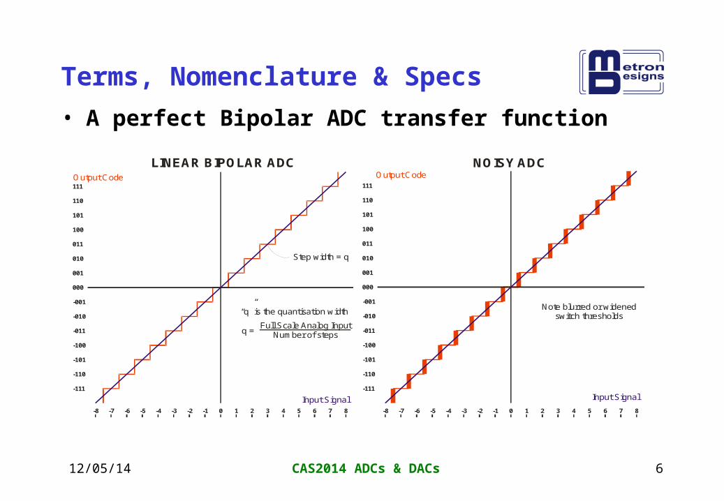
• A perfect Bipolar ADC transfer function
Input Signal
Output Code
001
000
010
100
011
101
110
111
-111
-110
-100
-101
-011
-010
-001
0-1-2-3-4-5-6-7-8 1 2 3 4 5 6 7 8
LINEAR BIPOLAR ADC
Step width = q
“q” is the quantisation width
q =Full Scale Input Analog
Number of steps
Input Signal
Output Code
001
000
010
100
011
101
110
111
-111
-110
-100
-101
-011
-010
-001
0-1-2-3-4-5-6-7-8 1 2 3 4 5 6 7 8
NOISY ADC
Note blurred or widenedswitch thresholds
12/05/14 CAS2014 ADCs & DACs 7
Terms, Nomenclature & Specs
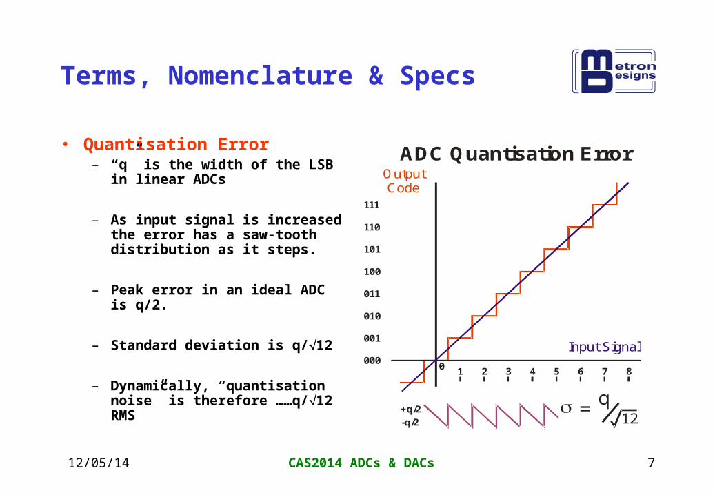
• Quantisation Error– “q” is the width of the LSB in
linear ADCs
– As input signal is increased the error has a saw-tooth distribution as it steps.
– Peak error in an ideal ADC is q/2.
– Standard deviation is q/12
– Dynamically, “quantisation noise” is therefore ……q/12 RMS
Input Signal
OutputCode
001
000
010
100
011
101
110
111
0 1 2 3 4 5 6 7 8
ADC Quantisation Error
+q/2-q/2
=q
12
12/05/14 CAS2014 ADCs & DACs 8
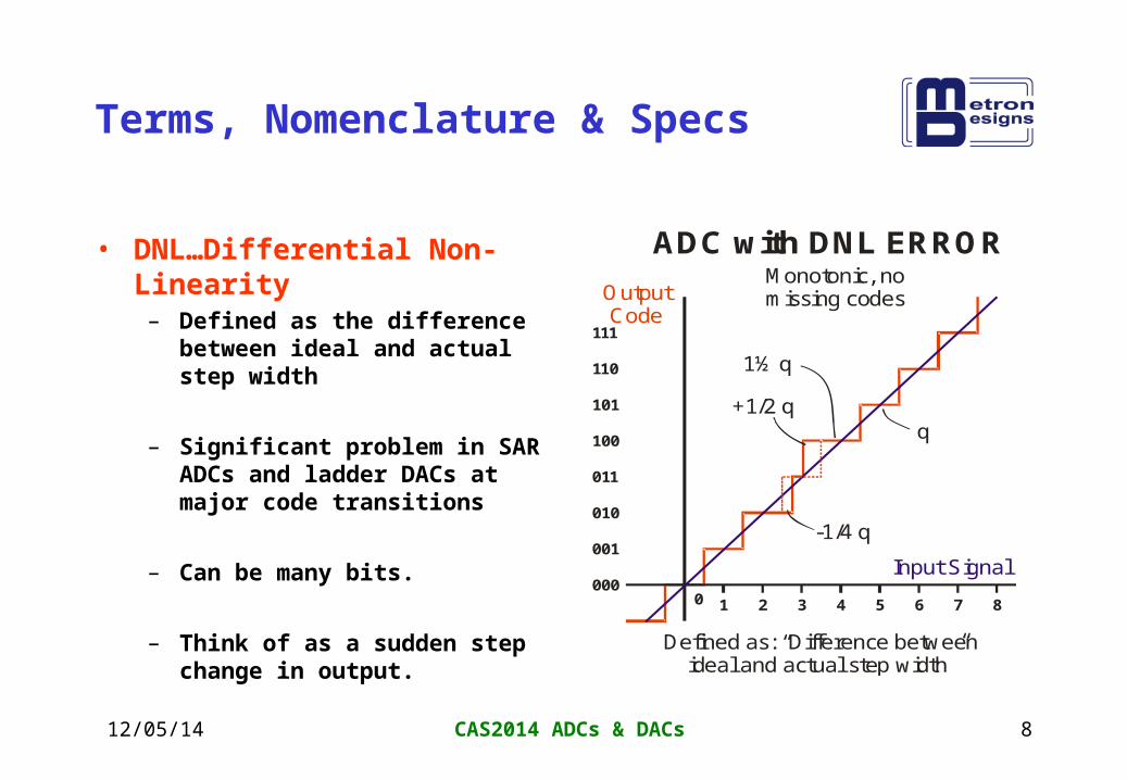
Terms, Nomenclature & Specs
• DNL…Differential Non-Linearity
– Defined as the difference between ideal and actual step width
– Significant problem in SAR ADCs and ladder DACs at major code transitions
– Can be many bits.
– Think of as a sudden step change in output.
Input Signal001
000
010
100
011
101
110
111
0 1 2 3 4 5 6 7 8
ADC with DNL ERROR
OutputCode
+1/2 q
-1/4 q
Defined as: “Difference betweenideal and actual step width”
q
1½ q
Monotonic, nomissing codes
12/05/14 CAS2014 ADCs & DACs 9
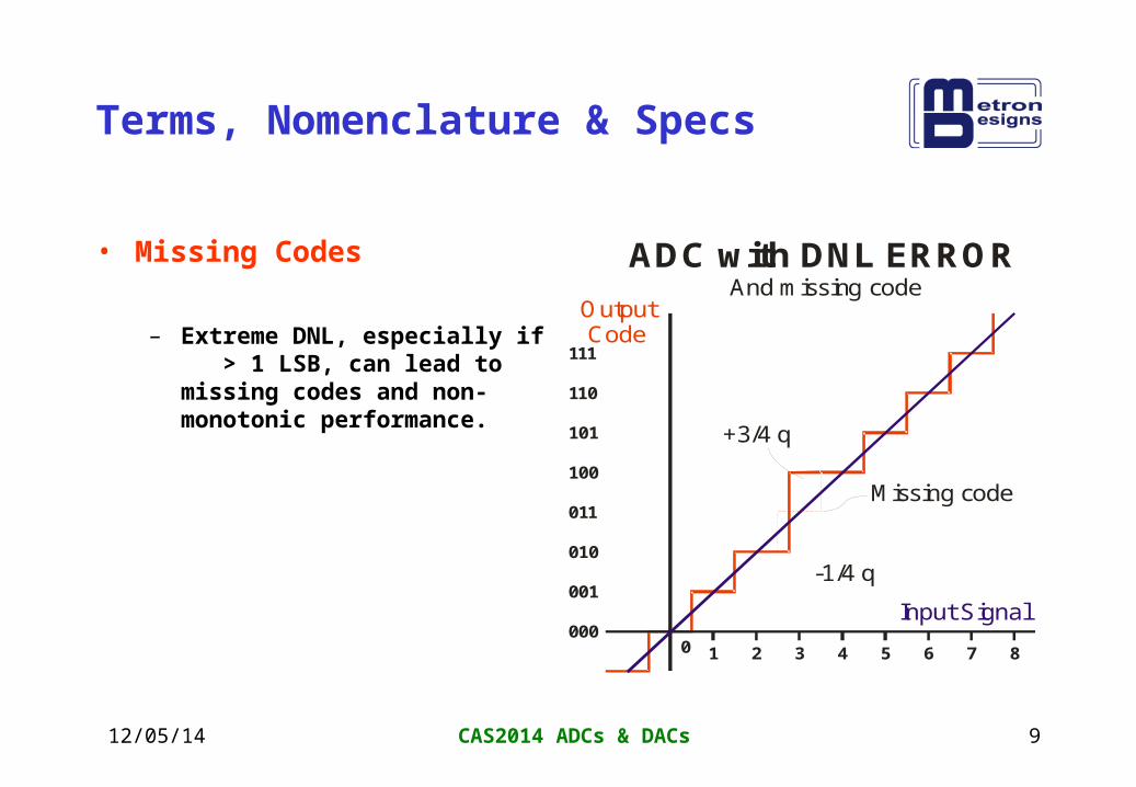
Terms, Nomenclature & Specs
• Missing Codes
– Extreme DNL, especially if > 1 LSB, can lead to missing codes and non-monotonic performance.
Input Signal001
000
010
100
011
101
110
111
0 1 2 3 4 5 6 7 8
ADC with DNL ERROR
Missing code
OutputCode
+3/4 q
-1/4 q
And missing code
12/05/14 CAS2014 ADCs & DACs 10
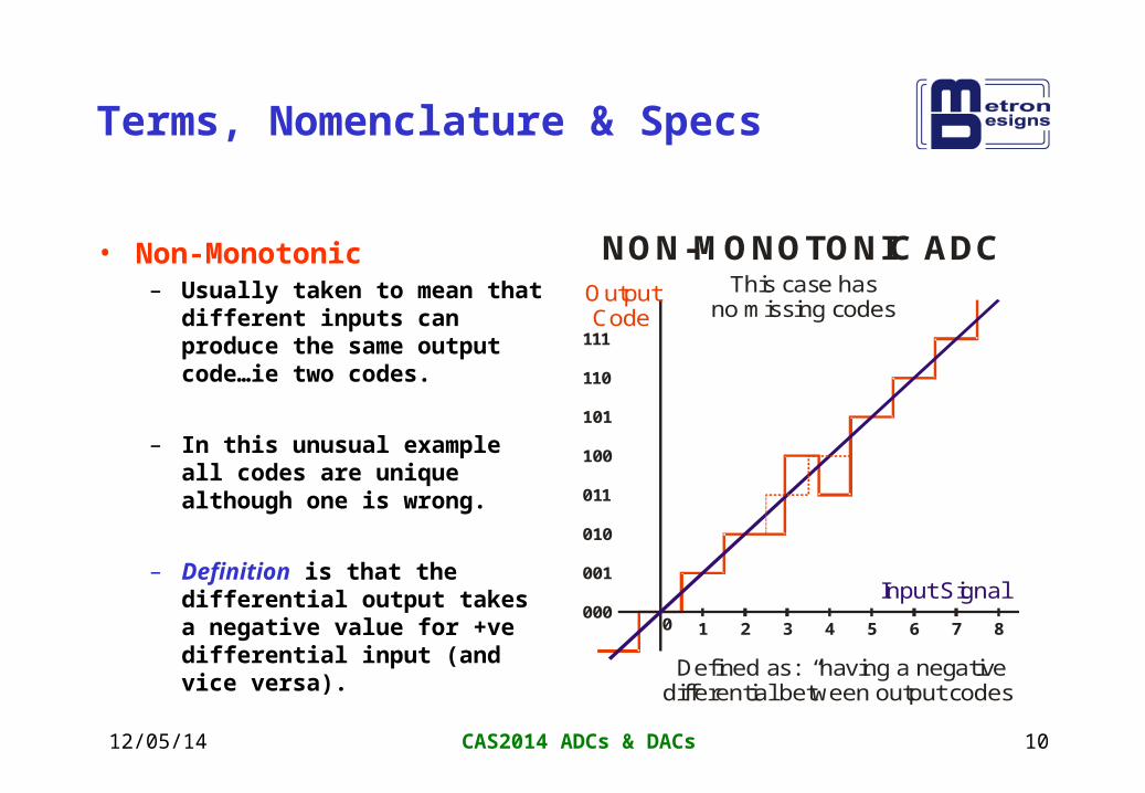
Terms, Nomenclature & Specs
• Non-Monotonic– Usually taken to mean that
different inputs can produce the same output code…ie two codes.
– In this unusual example all codes are unique although one is wrong.
– Definition is that the differential output takes a negative value for +ve differential input (and vice versa).
Input Signal
OutputCode
001
000
010
100
011
101
110
111
0 1 2 3 4 5 6 7 8
NON-MONOTONIC ADC
Defined as: “having a negative differential between output codes”
This case hasno missing codes
12/05/14 CAS2014 ADCs & DACs 11
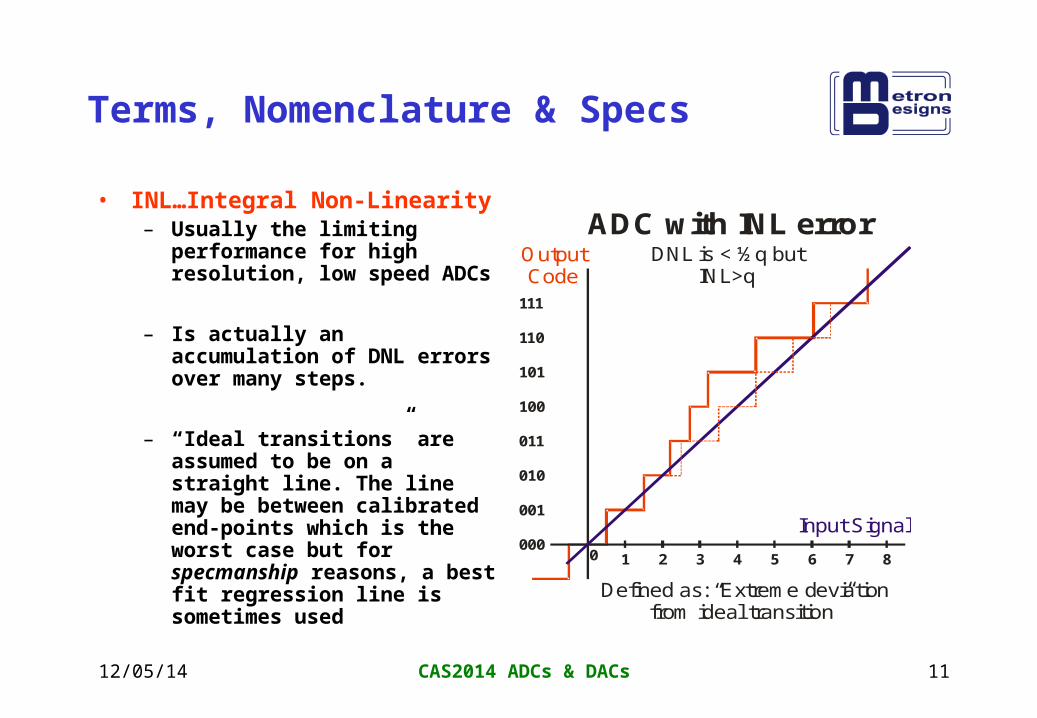
Terms, Nomenclature & Specs
• INL…Integral Non-Linearity– Usually the limiting
performance for high resolution, low speed ADCs
– Is actually an accumulation of DNL errors over many steps.
– “Ideal transitions” are assumed to be on a straight line. The line may be between calibrated end-points which is the worst case but for specmanship reasons, a best fit regression line is sometimes used
Input Signal
OutputCode
001
000
010
100
011
101
110
111
0 1 2 3 4 5 6 7 8
ADC with INL errorDNL is < ½q but
INL>q
Defined as: “Extreme deviationfrom ideal transition”
12/05/14 CAS2014 ADCs & DACs 12
Terms, Nomenclature & Specs
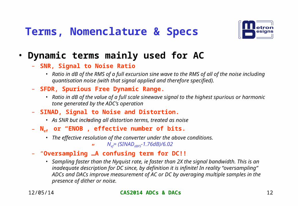
• Dynamic terms mainly used for AC– SNR, Signal to Noise Ratio
• Ratio in dB of the RMS of a full excursion sine wave to the RMS of all of the noise including quantisation noise (with that signal applied and therefore specified).
– SFDR, Spurious Free Dynamic Range.• Ratio in dB of the value of a full scale sinewave signal to the highest spurious or
harmonic tone generated by the ADC’s operation
– SINAD, Signal to Noise and Distortion.• As SNR but including all distortion terms, treated as noise
– Nef or “ENOB”, effective number of bits.
• The effective resolution of the converter under the above conditions.Nef= (SINADdBFS-1.76dB)/6.02
– “Oversampling”…A confusing term for DC!!• Sampling faster than the Nyquist rate, ie faster than 2X the signal bandwidth. This is an
inadequate description for DC since, by definition it is infinite! In reality “oversampling” ADCs and DACs improve measurement of AC or DC by averaging multiple samples in the presence of dither or noise.
12/05/14 CAS2014 ADCs & DACs 13
Flash ADCs
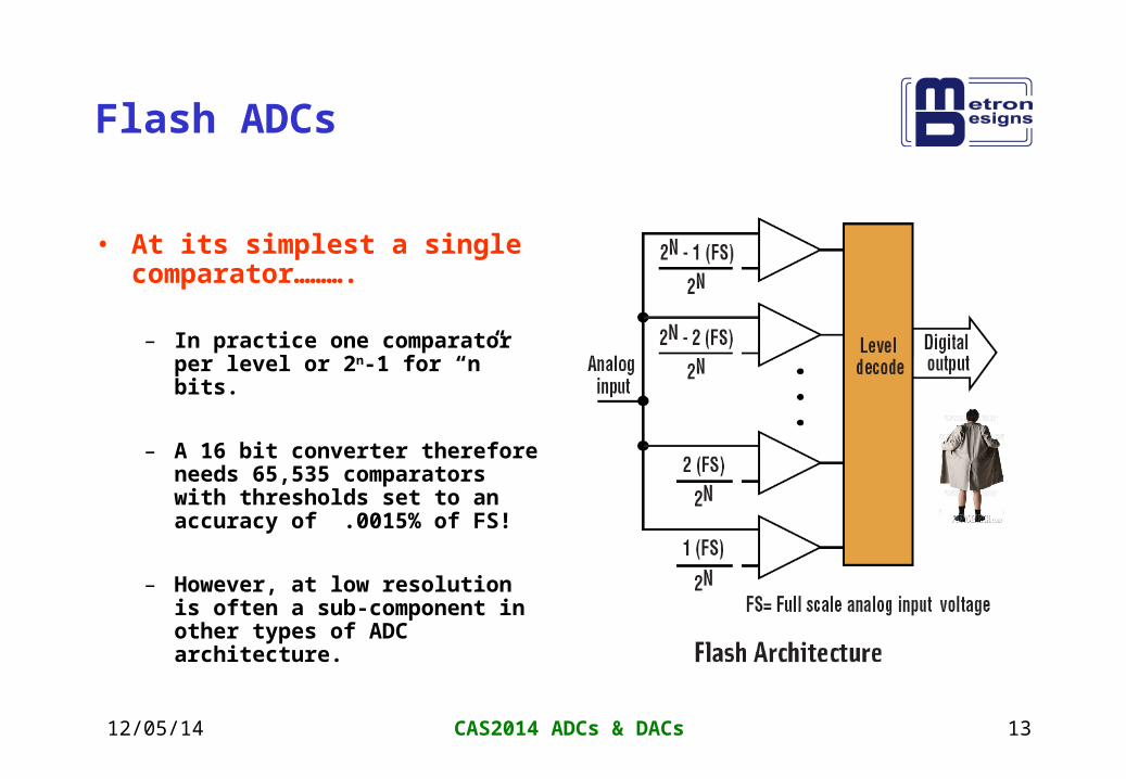
• At its simplest a single comparator……….
– In practice one comparator per level or 2n-1 for “n” bits.
– A 16 bit converter therefore needs 65,535 comparators with thresholds set to an accuracy of .0015% of FS!
– However, at low resolution is often a sub-component in other types of ADC architecture.
12/05/14 CAS2014 ADCs & DACs 14
Flash ADCs, characteristics
• The flash ADC is one of the few types that does not include a DAC in a feedback loop– This means that there is the shortest possible path between
signal and output, ie between Analogue and Digital.• Flash converters are very fast, the fastest available.
• They have very short delays, (latency or group delay) as well as high bandwidth.
• They are therefore relatively easy to integrate into feedback loops.
• They are used within both Pipeline and - converters.
12/05/14 CAS2014 ADCs & DACs 15
Pipeline Converters
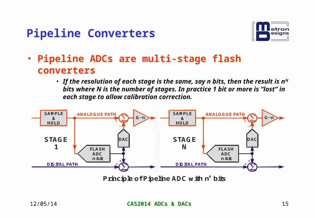
• Pipeline ADCs are multi-stage flash converters• If the resolution of each stage is the same, say n bits, then the result is nN
bits where N is the number of stages. In practice 1 bit or more is “lost” in each stage to allow calibration correction.
SAMPLE&
HOLD
FLASHADCn-bit
DAC
G~n
DIGITAL PATH
ANALOGUE PATH
+_
++
STAGE1
SAMPLE&
HOLD
FLASHADCn-bit
DAC
G~n
DIGITAL PATH
ANALOGUE PATH
+_
++
STAGEN
Principle of Pipeline ADC with n bitsN
12/05/14 CAS2014 ADCs & DACs 16
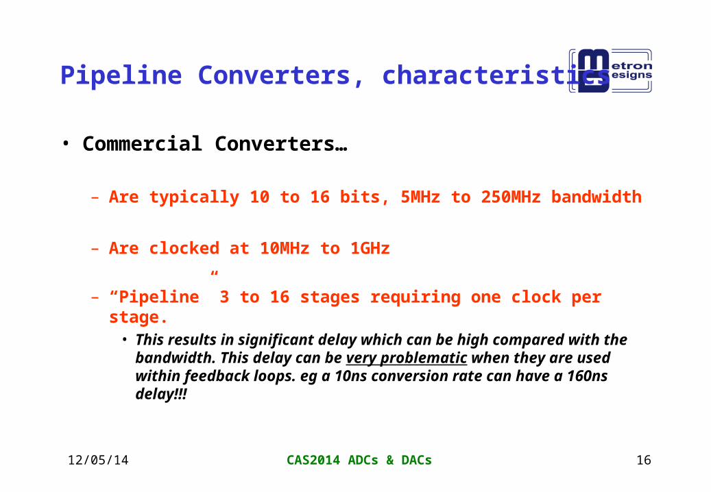
Pipeline Converters, characteristics
• Commercial Converters…
– Are typically 10 to 16 bits, 5MHz to 250MHz bandwidth
– Are clocked at 10MHz to 1GHz
– “Pipeline” 3 to 16 stages requiring one clock per stage.• This results in significant delay which can be high compared
with the bandwidth. This delay can be very problematic when they are used within feedback loops. eg a 10ns conversion rate can have a 160ns delay!!!
12/05/14 CAS2014 ADCs & DACs 17
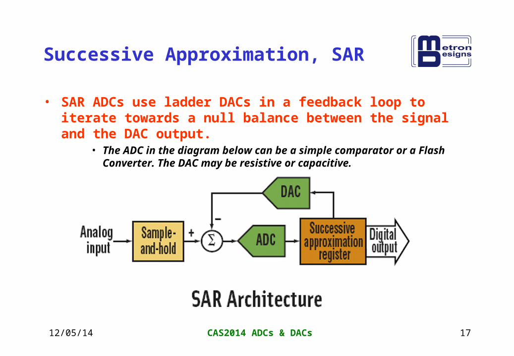
Successive Approximation, SAR
• SAR ADCs use ladder DACs in a feedback loop to iterate towards a null balance between the signal and the DAC output.
• The ADC in the diagram below can be a simple comparator or a Flash Converter. The DAC may be resistive or capacitive.
12/05/14 CAS2014 ADCs & DACs 18
SAR, operation and characteristics
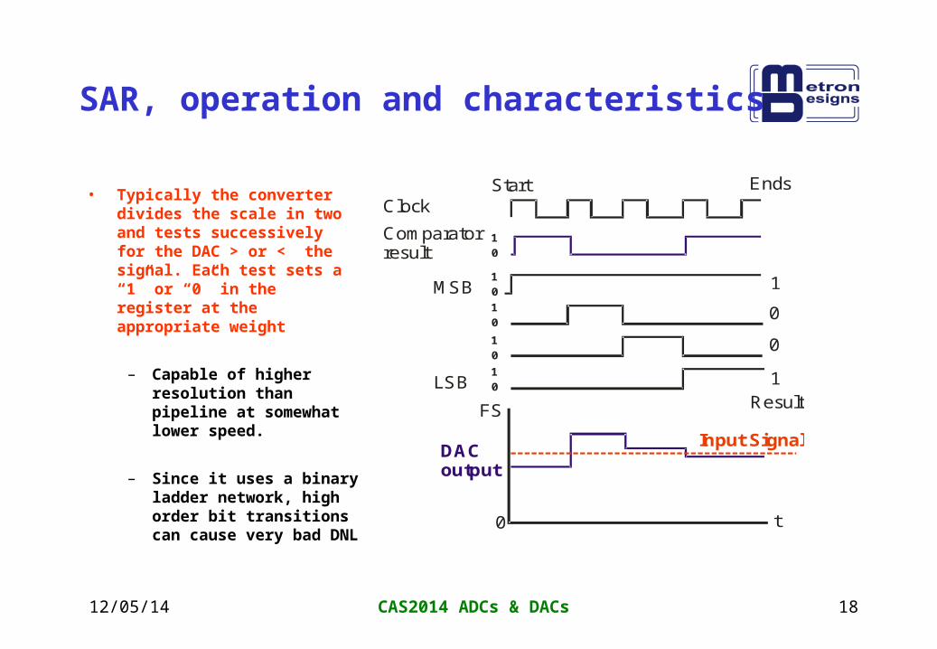
• Typically the converter divides the scale in two and tests successively for the DAC > or < the signal. Each test sets a “1” or “0” in the register at the appropriate weight
– Capable of higher resolution than pipeline at somewhat lower speed.
– Since it uses a binary ladder network, high order bit transitions can cause very bad DNL
Clock
Comparatorresult
MSB
LSB
DACoutput
FS
t
Result
1
0
0
1
Start Ends
10
10
10
10
10
Input Signal
0
12/05/14 CAS2014 ADCs & DACs 19
Charge Balance, Dual-slope
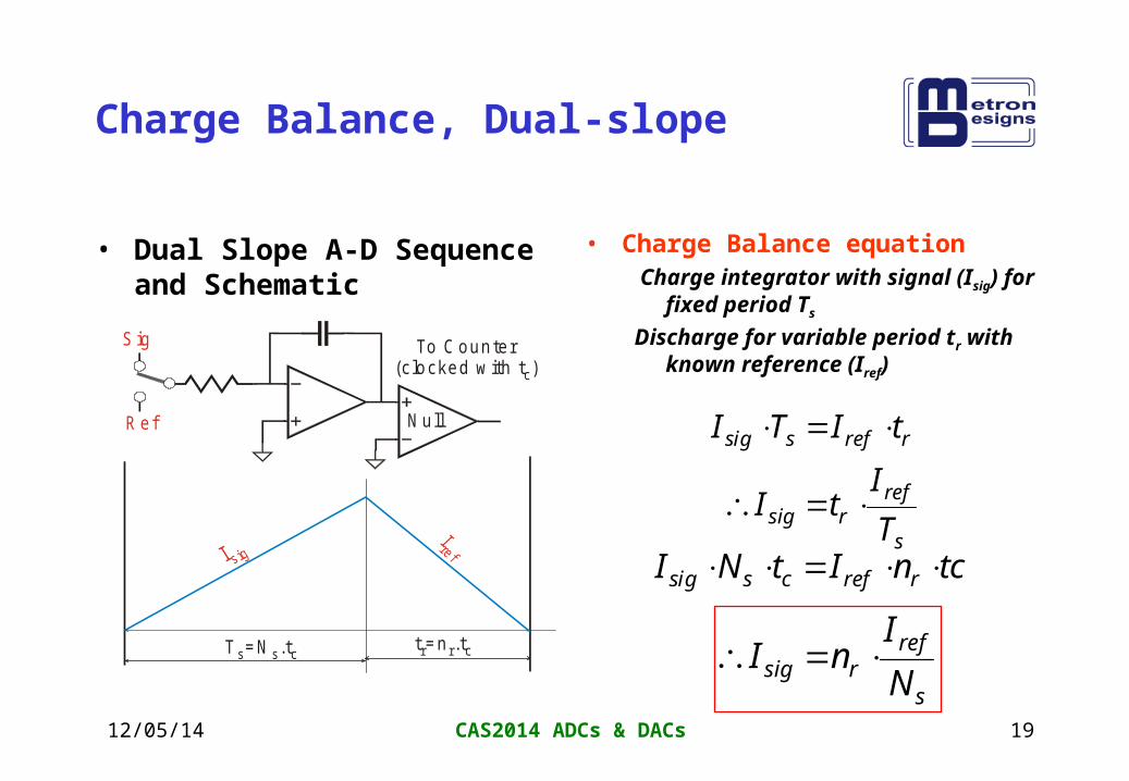
• Dual Slope A-D Sequence and Schematic
• Charge Balance equation Charge integrator with signal (Isig)
for fixed period Ts
Discharge for variable period tr with known reference (Iref)
t =n .tr r c
Sig
N ull
T =N .ts s c
To C ounter(clocked w ith t )c
R efrrefssig tITI
tcnItNI rrefcssig
s
refrsig T
ItI
s
refrsig N
InI
12/05/14 CAS2014 ADCs & DACs 20
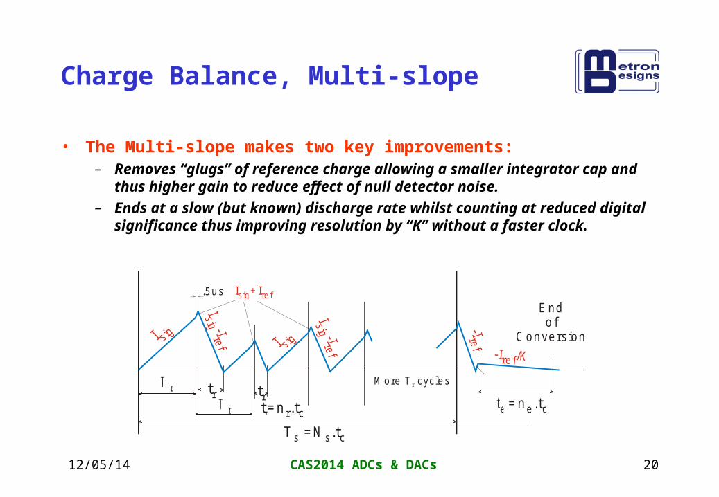
Charge Balance, Multi-slope
• The Multi-slope makes two key improvements:– Removes “glugs” of reference charge allowing a smaller integrator cap and
thus higher gain to reduce effect of null detector noise. – Ends at a slow (but known) discharge rate whilst counting at reduced digital
significance thus improving resolution by “K” without a faster clock.
I + Isig ref.5us
T r
T r te =n .te c
tr trt =n .tr r c
T =N .ts s c
M ore T cyclesr
Endof
Conversion
12/05/14 CAS2014 ADCs & DACs 21
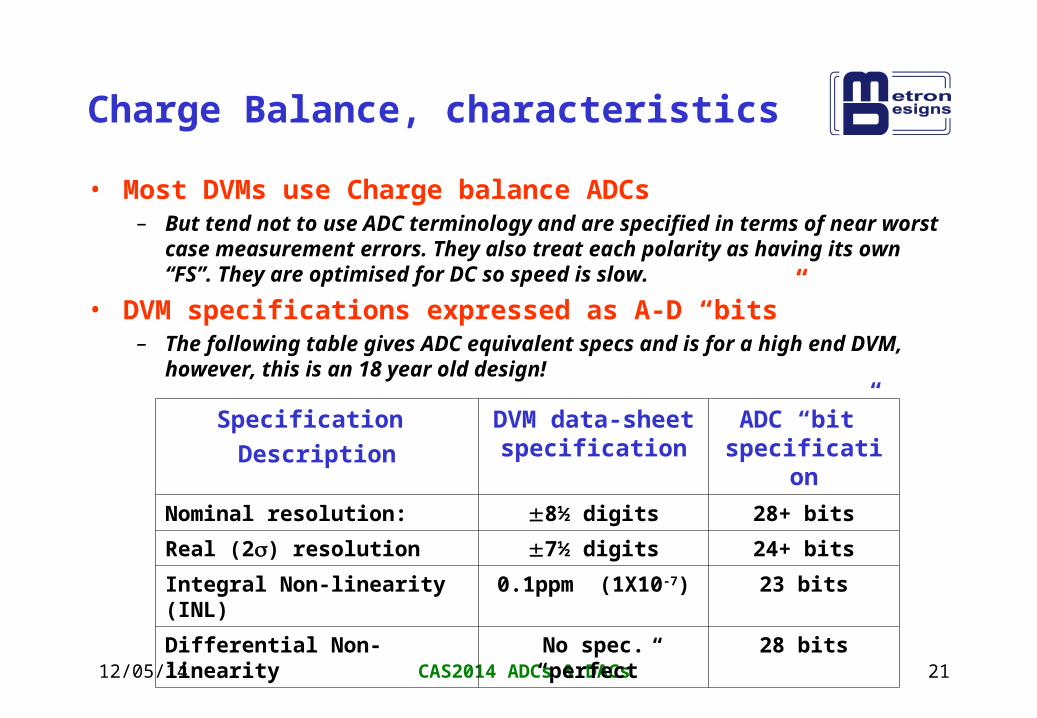
Charge Balance, characteristics
• Most DVMs use Charge balance ADCs– But tend not to use ADC terminology and are specified in terms of near worst
case measurement errors. They also treat each polarity as having its own “FS”. They are optimised for DC so speed is slow.
• DVM specifications expressed as A-D “bits”– The following table gives ADC equivalent specs and is for a high end DVM,
however, this is an 18 year old design!
Specification
Description
DVM data-sheet specification
ADC “bit” specification
Nominal resolution: 8½ digits 28+ bits
Real (2) resolution 7½ digits 24+ bits
Integral Non-linearity (INL) 0.1ppm (1X10⁻⁷) 23 bits
Differential Non-linearity No spec. “perfect” 28 bits
12/05/14 CAS2014 ADCs & DACs 22
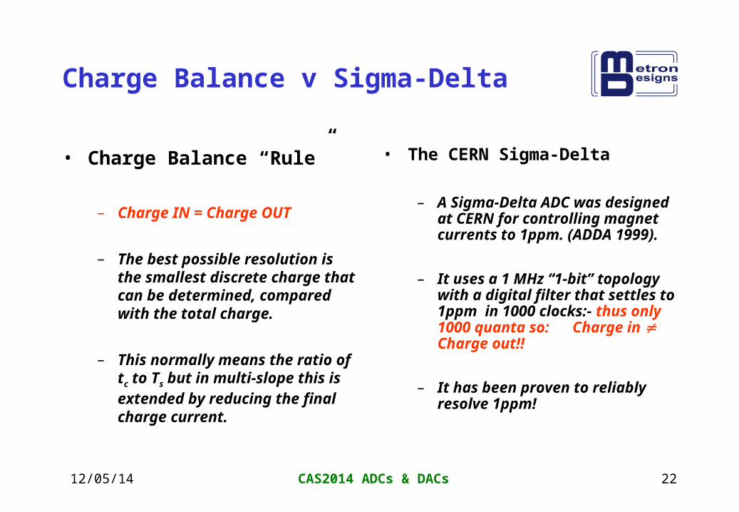
Charge Balance v Sigma-Delta
• Charge Balance “Rule”
– Charge IN = Charge OUT
– The best possible resolution is the smallest discrete charge that can be determined, compared with the total charge.
– This normally means the ratio of tc to Ts but in multi-slope this is extended by reducing the final charge current.
• The CERN Sigma-Delta
– A Sigma-Delta ADC was designed at CERN for controlling magnet currents to 1ppm. (ADDA 1999).
– It uses a 1 MHz “1-bit” topology with a digital filter that settles to 1ppm in 1000 clocks:- thus only 1000 quanta so:
Charge in Charge out!!
– It has been proven to reliably resolve 1ppm!
12/05/14 CAS2014 ADCs & DACs 23
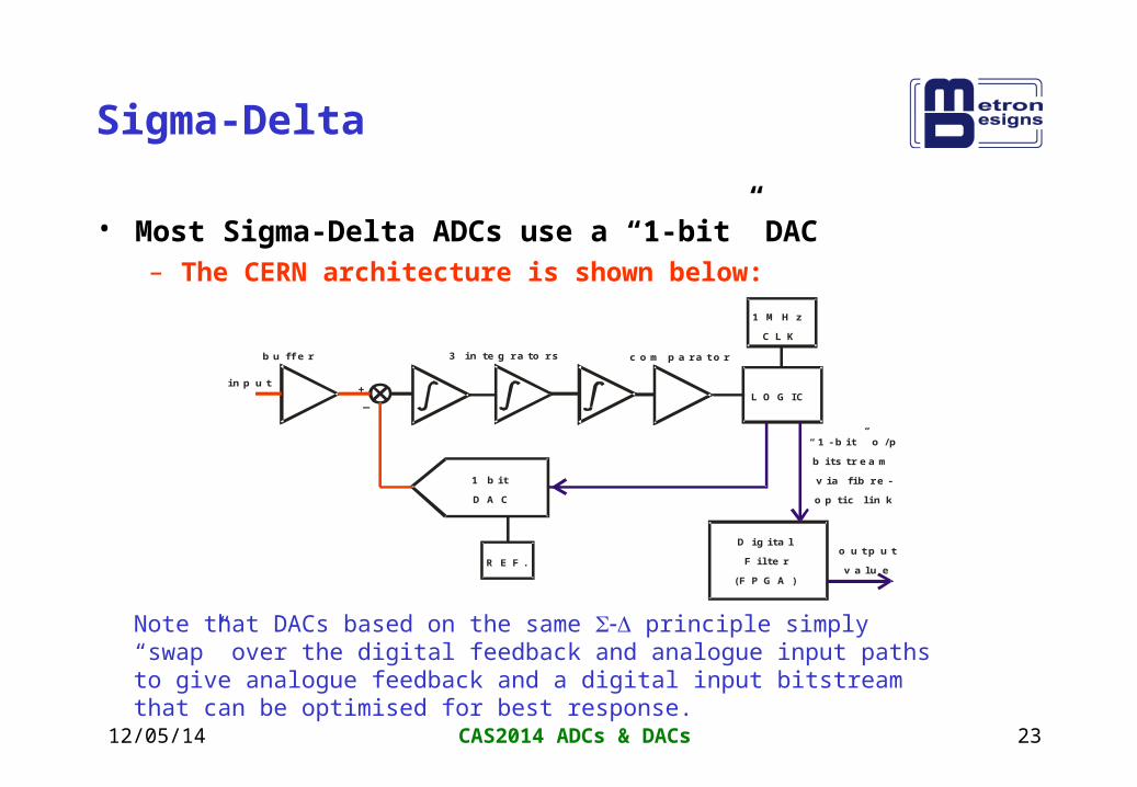
Sigma-Delta
• Most Sigma-Delta ADCs use a “1-bit” DAC – The CERN architecture is shown below:
Note that DACs based on the same principle simply “swap” over the digital feedback and analogue input paths to give analogue feedback and a digital input bitstream that can be optimised for best response.
b u f f e r 3 i n t e g r a t o r s c o m p a r a t o r
L O G I C
D A C
“ 1 - b i t ” o / p
b i t s t r e a m
v i a f i b r e -
o p t i c l i n k
i n p u t
1 b i t
1 M H z
C L K
R E F .
D i g i t a l
F i l t e r
( F P G A )
o u t p u t
v a l u e
+_
12/05/14 CAS2014 ADCs & DACs 24
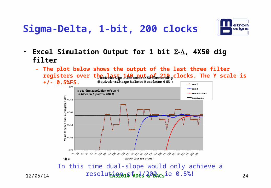
Sigma-Delta, 1-bit, 200 clocks
• Excel Simulation Output for 1 bit , 4X50 dig filter– The plot below shows the output of the last three filter registers over the last
140 out of 210 clocks. The Y scale is +/- 0.5%FS.
0.76
0.762
0.764
0.766
0.768
0.77
clock# (last 130 of 200)
Va
lue
fo
r e
ac
h s
um
ou
t re
gis
ter
(de
tail
)
sum2
sum3
sum4: Output
input value
1 bit Delta-Sigma 3rd order 4X50 filter settling(Equivalent Charge Balance Resolution 0.5%)
Note fine resolution of sum4 relative to 1 part in 200 !!
Fig 3
In this time dual-slope would only achieve a resolution of 1/200, ie 0.5%!
12/05/14 CAS2014 ADCs & DACs 25
Sigma-Delta characteristics
• Commercial Integrated Circuit (IC) converters– Mainly designed for audio frequency AC
• Therefore specs tend not to be DC & LF “friendly”• High manufacturing volume means low cost
– Bandwidths are DC to 1MHz• Noise-Resolution trade-off is readily available• Considerable delay “latency” in dig filter• But the digital filter can be tapped at different points and sampled
concurrently. This may allow “feed-forward” techniques to be used in loop controlled systems
– DC performance is usually limited…look carefully!• Although “24 bit” devices are claimed, the stability and linearity is really
in the 18 bit region for the best “merchant semiconductor” IC devices. INL is the limitation.
12/05/14 CAS2014 ADCs & DACs 26
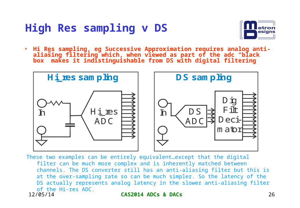
High Res sampling v DS
• Hi Res sampling, eg Successive Approximation requires analog anti-aliasing filtering which, when viewed as part of the adc “black box” makes it indistinguishable from DS with digital filtering
In
Hi_res sampling
In
DS sampling
Hi_resADC
DSADC
DigFilt
Deci-mator
These two examples can be entirely equivalent…except that the digital filter can be much more complex and is inherently matched between channels. The DS converter still has an anti-aliasing filter but this is at the over-sampling rate so can be much simpler. So the latency of the DS actually represents analog latency in the slower anti-aliasing filter of the Hi-res ADC.
12/05/14 CAS2014 ADCs & DACs 27
Sigma-Delta characteristics
• Problem Characteristics– “Idle tones”
• Bit patterns can repeat at low frequency if the loop does not “randomise” enough, a particular tendency in 3rd order or below.
• These are called tones because they show up as low level 1Hz-300 Hz lines in an FFT analysis of output.
• They are, at least in part, due to unwanted feedback in the modulator. PCB layout and supply filtering is critically important.
– “Sticky Zero”• Perhaps can be considered as a DC “idle tone” this shows up as a
tendency to maintain a symmetrical, zero condition, bit pattern in the modulator when operating just off zero. Synchronous noise, particularly in reference switching edges, is often the culprit.
12/05/14 CAS2014 ADCs & DACs 28
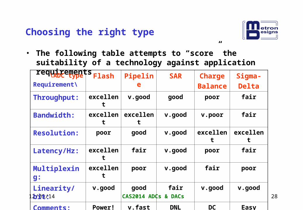
Choosing the right type
• The following table attempts to “score” the suitability of a technology against application requirements
\ADC type
Requirement\Flash Pipeline SAR Charge
Balance
Sigma-
Delta
Throughput: excellent v.good good poor fair
Bandwidth: excellent excellent v.good v.poor fair
Resolution: poor good v.good excellent excellent
Latency/Hz: excellent fair v.good poor fair
Multiplexing: excellent poor v.good fair poor
Linearity/bit: v.good good fair v.good v.good
Comments: Power!
Cost
v.fast
clock
DNL
stability
DC
only
Easy
Anti-alias
12/05/14 CAS2014 ADCs & DACs 29
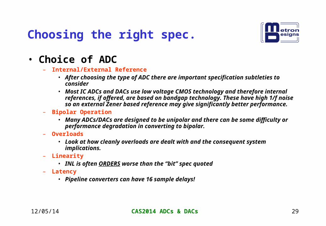
Choosing the right spec.
• Choice of ADC– Internal/External Reference
• After choosing the type of ADC there are important specification subtleties to consider
• Most IC ADCs and DACs use low voltage CMOS technology and therefore internal references, if offered, are based on bandgap technology. These have high 1/f noise so an external Zener based reference may give significantly better performance.
– Bipolar Operation• Many ADCs/DACs are designed to be unipolar and there can be some difficulty or
performance degradation in converting to bipolar.– Overloads
• Look at how cleanly overloads are dealt with and the consequent system implications.
– Linearity• INL is often ORDERS worse than the “bit” spec quoted
– Latency• Pipeline converters can have 16 sample delays!
12/05/14 CAS2014 ADCs & DACs 30
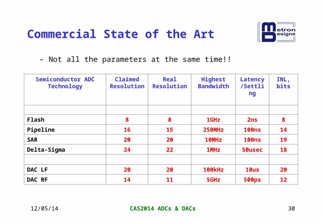
Commercial State of the Art
– Not all the parameters at the same time!!
Semiconductor ADC Technology
Claimed Resolution
Real Resolution
Highest Bandwidth
Latency /Settling
INL, bits
Flash 8 8 1GHz 2ns 8
Pipeline 16 15 250MHz 100ns 14
SAR 20 20 10MHz 100ns 19
Delta-Sigma 24 22 1MHz 50usec 18
DAC LF 20 20 100kHz 10us 20
DAC RF 14 11 5GHz 500ps 12
12/05/14 CAS2014 ADCs & DACs 31
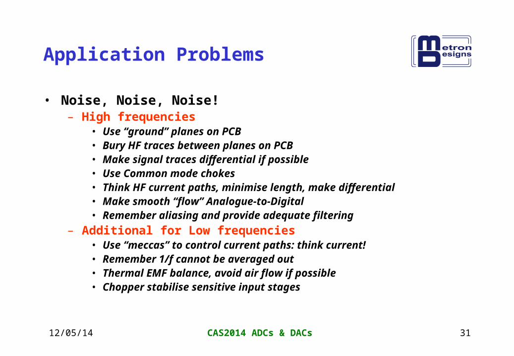
Application Problems
• Noise, Noise, Noise!– High frequencies
• Use “ground” planes on PCB• Bury HF traces between planes on PCB• Make signal traces differential if possible• Use Common mode chokes• Think HF current paths, minimise length, make differential• Make smooth “flow” Analogue-to-Digital• Remember aliasing and provide adequate filtering
– Additional for Low frequencies• Use “meccas” to control current paths: think current!• Remember 1/f cannot be averaged out• Thermal EMF balance, avoid air flow if possible• Chopper stabilise sensitive input stages
12/05/14 CAS2014 ADCs & DACs 32
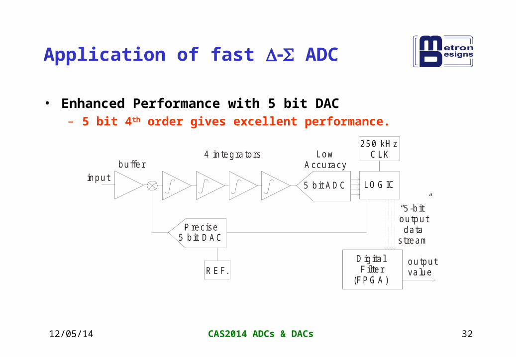
Application of fast ADC
• Enhanced Performance with 5 bit DAC– 5 bit 4th order gives excellent performance.
buffer 4 in tegrators Low
Accuracy
5 b it ADC LO G IC
DAC
“5-bit” outputdata
stream
input
5 b itP recise
250 kHz CLK
REF.D ig ita l F ilter
(FPG A)
outputvalue
12/05/14 CAS2014 ADCs & DACs 33
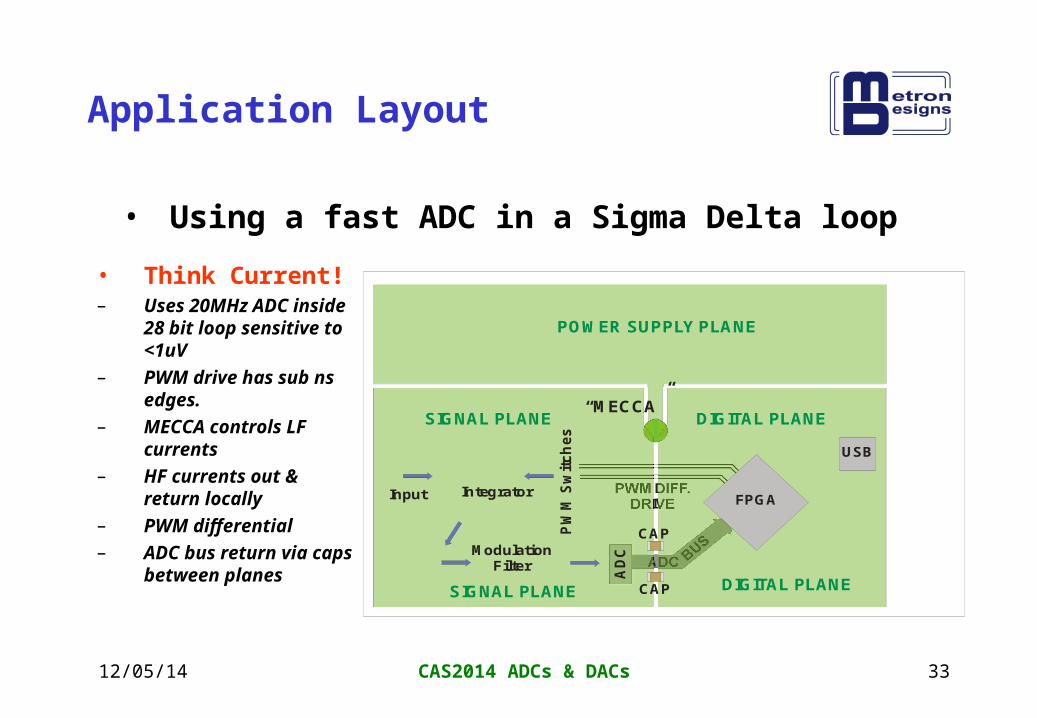
Application Layout
• Think Current!– Uses 20MHz ADC
inside 28 bit loop sensitive to <1uV
– PWM drive has sub ns edges.
– MECCA controls LF currents
– HF currents out & return locally
– PWM differential
– ADC bus return via caps between planes
PWM DIFF.DRIVE
ADC
FPGA
“MECCA”
USB
Input
PW
M S
wit
ch
es
Integrator
ModulationFilter
SIGNAL PLANE
SIGNAL PLANE
POWER SUPPLY PLANE
DIGITAL PLANE
DIGITAL PLANE
CAP
CAP
AD
C
• Using a fast ADC in a Sigma Delta loop
12/05/14 CAS2014 ADCs & DACs 34
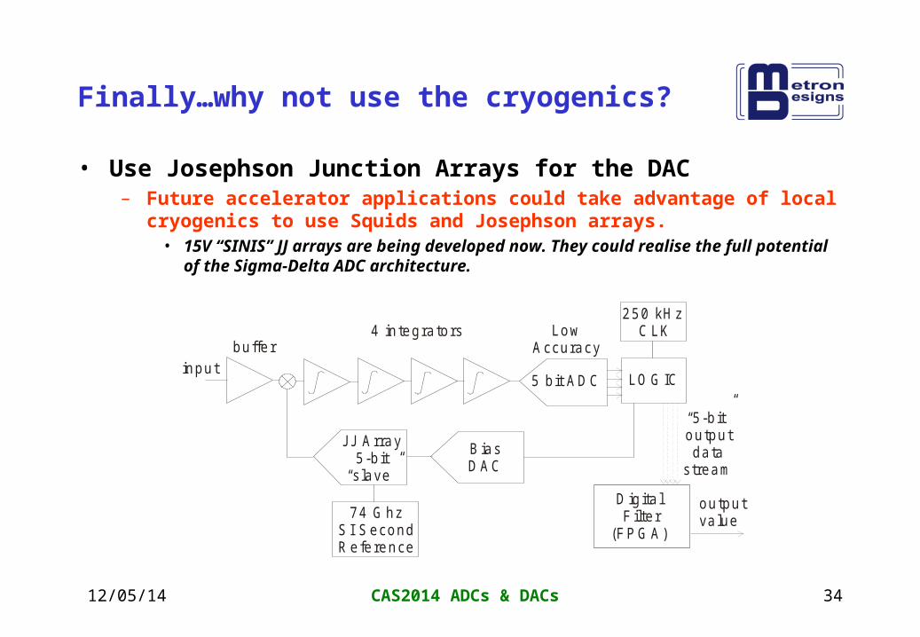
Finally…why not use the cryogenics?
• Use Josephson Junction Arrays for the DAC– Future accelerator applications could take advantage of local cryogenics to
use Squids and Josephson arrays.• 15V “SINIS” JJ arrays are being developed now. They could realise the full
potential of the Sigma-Delta ADC architecture.
buffer 4 in tegrators Low
Accuracy
5 b it ADC LO G IC
“5-bit” outputdata
stream
input
JJ A rray5-bit
“slave”
B iasDAC
250 kHz C LK
74 G hzSI SecondReference
D ig ita l F ilter
(FPG A)
outputvalue
12/05/14 CAS2014 ADCs & DACs 35
Conclusions
• Modern “single chip” ADCs, though difficult to use and optimise, offer outstanding performance for the cost.
• NEVER underestimate the difficulties in realising the datasheet promises.• For DC & LF metrology, Delta-Sigma ICs can achieve circa 2 ppm noise and
linearity performance.• A custom designed Delta-Sigma has been incorporated in a Temperature Bridge
and achieves .05ppm linearity.• A SINIS JJ array can be integrated in a Delta-Sigma loop to form a Quantum
Voltmeter with sub ppm resolution.
• Thank you!
• Reference 1: Oversampling Delta-Sigma Data Converters: Theory, Design, and Simulation (Paperback) by James C. Candy (Editor), Gabor C. Temes (Editor) . ISBN 0-87942-285-8 IEEE Press, Wiley. In stock Amazon.