Embed Size (px)
Citation preview
/4\11"~1 l,
~1.:-.'·il ·· .;.· ·_.\: ..
• . ,, ! • -t. I : .•.. ,· -'\ .. --·· j . .}
'.~3/
23 March 2010
ICOD: 1 December 2009
DIA-08-1003-011
UNCLASSIFIED/fP8R err1e1Rt U9E OIILI
Defense Intelligence Reference Document Acquisition Threat Support
Metallic Spintronics
UNCLASSIFIED/,«FOII: OPFilltftk Wil OPHa\t

UNCLASSIFIED,l/FOR OFFICIO! 1155 At'! Y
Metallic Spintronics
Prepared by:
(b)(3):10 USC 424
gency
Author:
Administrative Note
COPYRIGHT WARNING: Further dissemlnatlon of the photographs in this publication is not authorized.
This product is one in a series of advanced technology reports produced in FY 2009 under the Defense Intelligence Agency, J<b)(3):10 USC 424 I Advanced Aerospace Weapon System Applications (AAWSA)rogram. Comments or questions pertaining to this document should be addressed to b 3 :10 USC 424· b 6 AAWSA Program Manager, Defense Intelligence Agency, ATTN: b 3 :10 use 42 Bldg 6000, Washington, DC 20340-5100.
ii UNCLASSIFIED/ (FOR OFFICICP 11S6 QlllzY
UNCLASSIFIED//&OA O&&I&l,.k WiE 8Pll.lf
Contents
1. Introduction ....................................................................................................... iv
2. Giant Magnetoresistance .................................................................................... 1
2.1 GMR Basics .................................................................................................... 1
2.2 GMR Applications ........................................................................................ 3
3. Spin-Transfer-Torque •.•••••••••••••••••.••••••.••.•.••••..•...•••••.••..••....•.••••••••••••••••••••.•••••••• 4
3.1 STT Basics .................................................................................................................. 4
3.2 STT Experiments ••••••••••••••••••••••••••••••••••••••••••••••••••••••••••••••••••••••••••••••••••••••••• 7
3.3 STT Applications ........................................................................................ 10
3.4 STT-Driven Motion of Magnetic Domain Walls ........................................... 12
4. Antiferromag netic Metal Spintro,n ics ................................................................ 12
4.1 Antiferromag netic GM R ............................................................................. 13
4.2 Antiferromagnetic STT ............................................................................... 14
S. Summary and Conclusion~ ............................................................................... 16
6. References ................... , .......................................................................................... 18
Figures
Figure 1. In a Magnetic Multilayer, Several Atomic Layers of Magnetic Material Alternate With Layers of Nonmagnetic Material ...................................... 1
Figure 2. Resistance of a Magnetic Multilayer R Versus Magnetic Field ................... 2 Figure 3. Differential Resistance dV/dI of a Mechanical Point Contact as a Function
of Current for a Series of Magnetic Fields ................................................ 4 Figure 4. Device Schematics for STT Experiments .................................................. s Figure 5. Qualitative Picture of STT ........................................................................ 6 Figure 6. Torques on a Magnetic Moment in a Magnetic Field and Subject to an
Electrica I Current ..................................................................................... 7 Figure 7. Spin-Torque-Driven Magnetic Switching .................................................. 8 Figure 8. Oscillatory Voltage .................................................................................. 9 Figure 9. Scanning Transmission X-ray Microscopy Images ................................. 10 Figure 10. Conventional MRAM Cell ...................................................................... 11 Figure 11. Racetrack Memory Concept ................................................................. 12 Figure 12. Schematic of Point Contact to Sample Geometry ................................. 15
iii UNCLASSIFIED//POfl 8PPl@ltlil: lt!!IE OHi!¥

UNCLASSIFIED//EOR AEEJCJOP !PSF ON!~
Metallic Spintronics
1. Introduction
The rapid pace of progress in the computer industry over the past 40 years has been based on the miniaturization of chips and other computer components. Further miniaturization, however, faces serious challenges-for example, increasingly high power dlsslpation. To continue on pace, the industry must go beyond incremental improvements and embrace radically new technologies. A promising nanoscale technology known as spintronics (a neologism for "spinbased electronicsu) has emerged. Spintronics refers to the role an electron spin plays in solid-state physics. Spintronics researchers aim to develop a revolutionary new class of electronic devices based on the spin of electrons in addition to the charge. In spintronic devices, information is carried not by the electron's charge, as in conventional microchips, but by the electron's intrinsic spin. Changing the spin of an electron is faster and requires less power than moving it. Therefore, if a reliable way could be found to control and manipulate spins, spintronic devices could offer higher data processing speeds, lower electricity consumption, and many other advantages over conventional chips, perhaps including the ability to carry out radically new quantum computations.
Spintronics in ferromagnetic systems is built on a complementary set of phenomena in which the magnetic configuration of the system influences its transport properties and vice versa. Giant magnetoresistance (GMR) (Reference 1, 2) and spin-transfer-torque {STT) (Reference 3-5) phenomena exemplify such interconnections in multilayers composed of ferromagnetic (F) and nonmagnetic (N) layers. The physics and applications of metal lie spfntronics are discussed in this report from the perspective of these two phenomena. GMR, research on which was awarded the Nobel Prize in Physics in 2007, refers to a large change in resistance of magnetic multilayers when the relative orientation of magnetic moments in their constituent ferromagnetic layers is altered by an applied magnetic field. The inverse effect, STT, in which a large electrical current density j can perturb the magnetic state of a multilayer, has also been predicted (Reference 3, 4) and observed in experiments on current-induced reversal and precession of magnetization (Reference 5-9) and magnetic domain wall motion (Reference 10, 11).
iv
UNCLASSIFIE:D/,'P8N 8PPleIAt 09£ Gilli
UNCLASSIFIED;/P8fl.. 8PPl81AL ltDI!! fJHLY
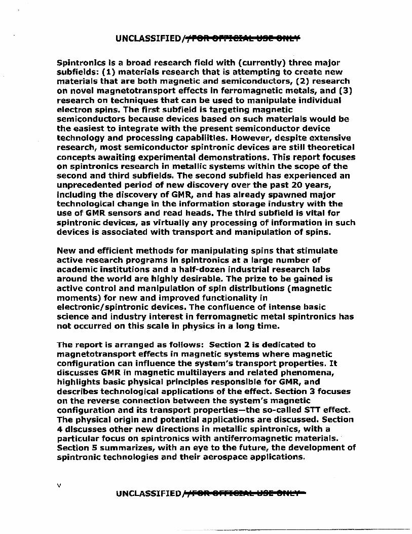
Spintronics is a broad research field with ( currently) three major subfields: ( 1) materials research that is attempting to create new materials that are both magnetic and semiconductors, (2) research on novel magnetotransport effects in ferromagnetic metals, and (3) research on techniques that can be used to manipulate individual electron spins. The first subfield is targeting magnetic semiconductors because devices based on such materials would be the easiest to integrate with the present semiconductor device technology and processing capabilities. However, despite extensive research, most semiconductor spintronic devices are still theoretical concepts awaiting experimental demonstrations. This report focuses on spintronics research in metallic systems within the scope of the second and third subfields. The second subfield has experienced an unprecedented period of new discovery over the past 20 years, including the discovery of GM R, and has already spawned major technological change in the information storage industry with the use of GMR sensors and read heads. The third subfield is vital for spintronic devices, as virtually any processing of information in such devices is associated with transport and manipulation of spins.
New and efficient methods for manipulating spins that stimulate active research programs In spintronics at a large number of academic institutions and a half-dozen industrial research labs around the world are highly desirable. The prize to be gained is active control and manipulation of spin distributions (magnetic moments) for new and improved functionality in electronic/spintronic devices. The confluence of intense basic science and industry interest in ferromagnetic metal spintronics has not occurred on this scale in physics in a long time.
The report is arranged as follows: Section 2 is dedicated to magnetotransport effects in magnetic systems where magnetic configuration can influence the system's transport properties. It discusses GMR in magnetic multilayers and related phenomena, highlights basic physical principles responsible for GMR, and describes technological applications of the effect. Section 3 focuses on the reverse connection between the system's magnetic configuration and its transport properties-the so-called STT effect. The physical origin and potential applications are discussed. Section 4 discusses other new directions in metallic spintronics, with a particular focus on spintronics with antiferromagnetic materials. Section 5 summarizes, with an eye to the future, the development of spintronic technologies and their aerospace applications.
V
UNCLASSIFIED//P8R: BPPH!Ill.ih ~81! OHl:ltf
UNCLASSIFIED/JFOA OFF16l 1.k W&& &Hlk>S
2. Giant Magnetoresistance
2.1 GMR BASICS
This section discusses the phenomenon of giant magnetoresistance (GMR). Excellent reviews of GMR are available elsewhere (Reference 12-22). The focus on physical concepts important for the sections to follow are discussed.
GMR in magnetic multilayers refers to a dramatic reduction in the resistance of the multilayers when subjected to an external magnetic field. GMR's size is usually defined as the resistance change in magnetic field relative to its peak value. The effect can be distinguished from the ordinary magnetoresistance (MR) coming from the direct action of the magnetic field on the electron trajectories via the Lorentz force (Reference 23), and from the anisotropic MR, which comes from dependence of the resistivity on the relative orientation of magnetic moment to the current (Reference 24).
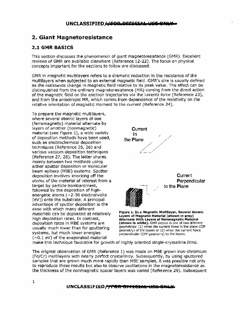
To prepare the magnetic multilayers, where several atomic layers of one (ferromagnetic) material alternate by layers of another (nonmagnetic) material (see Figure l)r a wide variety of deposition methods have been used, such as electrochemical deposition techniques (Reference 25, 26) and various vacuum deposition techniques (Reference 27, 28). The latter shares mainly between two methods using either sputter deposition or molecular beam epitaxy (MBE) systems. Sputter deposition involves knocking off the atoms of the material of interest from a target by particle bombardment, followed by the deposition of highenergetic atoms ( ~2-30 electronvolts [ eV]) onto the substrate. A principal advantage of sputter deposition is the ease with which many different materials can be deposited at relatively high deposition rates. In contrast, deposition rates in MBE systems are usually much lower than for sputtering systems, but much lower energies (~0.1 eV) of the evaporated material
Current In
the Plane
,,
Current Perpendicular
,, to the Plane
Figure 1, In a Magnetic Multilayer, Several Atomic Layers of Magnetic Material (shown in grey) Alternate With Layers of Nonmagnetic Material (shown in white). GMR occurs in one of two dlfferent geometries: (1) when the current flows in the plane (CIP geometry) of the layers or (2) when the current flows perpendicular (CPP geometry) to the layers.
make this technique favorable for growth of highly oriented single-crystalline films.
The original observation of GMR (Reference 1) was made on MBE grown iron-chromium (Fe/Cr) multilayers with nearly perfect crystallinity. Subsequently, by using sputtered samples that are grown much more rapidly than MBE samples, it was possible not only to reproduce these results but also to observe oscillations in the magnetoresistance as the thickness of the nonmagnetic spacer layers was varied (Reference 29). Subsequent
1 UNCLASSIFIED;; ret\ SPPH!IAb 1116& OPU.V

UNCLASSIFIED//FOR: OFFIGl1\L t.Hil! 8HI:¥
studies (Reference 30} on sputtered cobalt-copper (Co/Cu) multilayers revealed magnetoresistances at room temperatures 3 to 4 times larger than those for ironchromium and 13 times greater than those for the permalloy films that were used as magnetoresistive sensors in magnetic reading heads at that time. The much higher numbers observed in magnetic multilayers predetermined the fate of GMR in magnetic recording technology.
The current understanding is that GMR observed in magnetic multilayers arises from the dependence of the resistivity on their internal magnetic configuration and the role of the external magnetic field to change this configuration. Figure 2b illustrates GMR in the simple limit where the electron mean-free-path is much longer than the layer thicknesses. The electrical transport properties of the system are described in terms of the socalled two-current model (Reference 31), based on the suggestion by Mott (Reference 32) that, at temperatures lower than the Curie temperature, the spin-up and spin-down electrons will be almost independent and carry current in parallel. Electrons are much more strongly scattered by a magnetic layer if they and the local magnetization spin in opposite rather than the same direction (R > r). For simplicity, the figure is drawn with scattering only at interfaces; however, there is also scattering within the layers. At zero magnetic field, where the magnetizations of adjacent magnetic layers are aligned antiparallel-for example, because of exchange coupling between the layers (Reference 29)-the spin-down electrons are weakly scattered in layer
F1 F2
t J .. -L .. ..
t R R
~ ~ r r
RA
:..,R, -----(} '
Magnetic Field
F1 F2
I t ...... ___ ..... -
---· ........... ...
t R r
~· R
. •
F1 F2
t J ... t .. --· ' ·-~~- ·-~ .....
t r r
~ l R R
Figure 2, (a) Resistance of a magnetic multilayer R versus magnetic field. (b) Origin of GMR in terms of spin-dependent electron scattering: Fl and F2 are ferromagnetic layers with a nonmagnetic layer in between. At zero magnetic field, the magnetizations in Fl and F2 are aligned antiparallel (center panel) and can be switched to parallel orientation by an applied field. (c) The equivalent resistance circuits corresponding to the three magnetic configurations shown in (b). See text for details.
Fl but strongly scattered in F2. In contrast, the spin-up electrons are weakly scattered in layer F2 but strongly scattered in Fl. As a result, two channels are equivalent, leading to a total resistance in this "antiferromagnetic" configuration RAF= (R+r)/2 (see the corresponding resistance circuit in Figure 2c).
When the magnetizations of the two Flayers are set into parallel configuration by an applied magnetic field, the spin-up electrons are weakly scattered in both layers and form a low-resistivity channel, whereas the spin-down electrons are strongly scattered in all the layers and form a high-resistivity channel. The reversal of magnetic field just interchanges the roles of spin-up and spin-down channels. The current's shunting by the low-resistivity channel produces a low total resistance RF;;; 2Rr/(R+r} in this "ferromagnetic" configuration. The size of the GMR is defined as (RAF-RF}/RAF = (R-
2 UNCLASSIFIED/ f FOR OFEJCJ0P I PSF Al!! Y
UNCLASSIFIED//P81l 8PPM!I.AL ~81!! 8Hl!V
r)2/(R+r)2 5 1. The other definition l!R/R = (RAF-RF)/RF::;; (R-r)2/4Rr (unbounded from above) is also in use. Figure 2a shows a magnetoresistance curve typical for magnetic multilayers. The resistance is constant at a minimum value RF above a saturation field Bs (parallel Fs) and rises to a maximum value RAF as the applied magnetic field B approaches zero {antiparallel Fs).
GMR occurs in two different geometries (see Figure 1): namely when the current flows in the plane of the layers, or CIP geometry, or when current flows perpendicular to the layers, or CPP geometry. Most of experiments on GMR are carried out in the CIP geometry because measuring the fairly large resistance of a thin film is quite easy (film length is typically orders of magnitude larger than its thickness). Experiments in the CPP geometry are more difficult (Reference 33) and require special techniques for precision measurements of very small resistances ~10·7-10·8 n resulting from the "short and wide" geometry of a 1-mm2 "wide" and 1-µm "long" sample. In order to increase the resistances to easily observable values, microfabrication techniques can be used to reduce the sample's cross-sectional area (Reference 34-36). Finally, a simple and inexpensive point-contact technique (Reference 37) may also be suitable for this purpose. The samples with a reduced cross-sectional area will be of interest for spintransfer-torque experiments presented in Section 3,
2.2 GMR APPLICATIONS
GMR is currently used in magnetic field sensors, including those in read heads for computer hard drives, in galvanic isolators, and in nonvolatile random access memory devices. Reading information stored on magnetic hard disk drives in computers was the first large-scale commercial application of GMR. The information is stored by magnetizing small regions (magnetic domains) of a magnetic recording disk in different directions. The stray magnetic fields from these domains are detected by a GMR sensing element called spin valve. The simplest type of spin valve consists of two ferromagnetic layers separated by a thin, nonmagnetic spacer. The spin-valve resistance is smallest when the magnetizations of the two ferromagnetic layers are parallel and largest when the magnetizations are antiparallel. The antiparallel alignment is achieved by making the two layers respond differently to an external magnetic field; an antiferromagnet in contact with one of the layers is used to effectively "pin" the magnetization in this layer through an effect called "exchange bias. 1
' The exceptional responsiveness of spin valves to magnetic fields has enabled very high areal packing densities in hard drives.
Other sensor applications using GMR elements include monitoring of a ferrous gear rotation in machinery operation (Reference 38) via detection of a changing magnetic flux when a gear tooth passes near the sensor, monitoring of electrical current via detection of the current-induced Oersted magnetic field, and transferring highfrequency signals between isolated circuits (Reference 39) via magnetic fields generated by a high-frequency inductor in one circuit and replicated in another circuit by a GMR sensor.
3 UNCLASSIFIED/ 1 FAP 055JQI IL • ,tiii 8t1Wf J

UNCLASSIFIED//F&R &FFlll/11! ~81 8Hl:!V
3. Spin-Transfer-Torque
This section focuses on the spin-transfer-torque (STT) phenomenon, which refers to a novel method to control and manipulate magnetic moments in nanostructures by spin currents-one of the forefront and most exciting areas in magnetism research today.
3.1 STT BASICS
The previous section showed that the magnetic state of a ferromagnet can affect its electrical transport properties; for instance, the relative orientation of the magnetic moments in magnetic multilayers underlies the phenomenon of GMR (Reference 1, 2). The inverse effect, in which a large electrical current density can perturb the magnetic state of a multilayer, has also been predicted (Reference 3, 4). Here the current transfers vector spin between the magnetic layers and induces precession and/or reversal of the layer magnetizations. Altering the magnetic state with spin currents is based on quantum mechanical exchange interaction and represents a novel method of magnetization control on the nanometer length scale and the picosecond time scale.
The first observation of such a spintransfer phenomenon in magnetic multilayers was recorded by Tsoi et al. (Reference 5) (see Figure 3). In this experiment, the spin-transfer-induced excitations were produced by injecting high-density electrical currents into a Co/Cu magnetic multilayer through a mechanical point contact. Point contacts smaller than 10 nanometers (nm} are formed when a sharpened Cu metal wire (tip) is carefully brought into contact with the multilayer. The extremely small cross-sectional area of such a contact makes it possible to achieve current densities in excess of 1012 A/m 2• Because of its extremely small size ( < 10 nm), point contact is a very efficient probe of electrical transport properties in extremely small sample volumes inaccessible with other techniques (for example, electronbeam-lithography patterning). The
45 ,---,--_...--,---,----,.-.---...---.--.....---.----.---,
44
43
g 42
:g > 41 'C
40
39
V°(ST)
' (71) . i {6T)
. l (!>1)
I •
-10-
> -.S 12·
'> -6-
P,l)
! (2T) 00--2 -~4--6--8
. + µoH(T)
38------------------...._ ______ __. -0.03 -0.02 -0.01 0.00 0.01 0.02 0.03
VM Figure 3. Differential Resistance dV/dI of a Mechanical Point Contact as a Function of Current for a Series of Magnetic Fields. The peak in dV/dI indicates the onset of SST excitations_ The inset shows that the threshold current at the peak in dV/dl fncreases linearly wlth the applied field. (Reference 5)
latter qualifies point contact as the smallest probe of 57T today.
The STT phenomenon currently attracts considerable attention because it combines poorly understood fundamental science questions with the promise of applications in a broad range of technologies. In high-speed, high-density magnetic recording technology, for instance, SST could replace the Oersted field currently used for writing magnetic bits in storage media (for example, in magnetic random access memory [MRAM]). This may lead to a smaller and faster magnetic memory. Another possible application is based on the spin-transfer-induced precession of magnetization, which
4 • UNCLASSIFIED/ (FOB CEEJCICP us& 8Sllr_f

UNCLASSIFIED//509 OFFICiff L UEF 8Plklf
converts a direct current (de) voltage input into an alternating current (ac) voltage output. The frequency of such a precession can be tuned from a few gigahertz (GHz) to > 100 GHz by changing the applied magnetic field and/or de current, effectively resulting in a current-controlled oscillator for use in practical microwave circuits.
Since its prediction in 1996, the STT effect has been observed in a number of experiments, including those with mechanical (Reference 5, 9, 40) and lithographic point contacts (Reference 6, 41), manganite junctions (Reference 7), electrochemically grown nanowires (Reference 8), lithographically defined nanopillars (Reference 42, 43), tunnel junctions (Reference 44), and semiconductor structures (Reference 45). These different methods all share one characteristic feature: they make it possible to attain extremely high current densities (>10 12 A/m 2 for metallic structures) needed to produce sufficiently large spin-transfer torques (Reference 3, 4). This is achieved by forcing the electrical current to flow through a very small constriction. The latter can be a mechanical point contact, a lithographically defined point contact or nanopillar, or a nanowire, as illustrated in Figure 4. In all cases, the maximum current density jmax = I/A is defined by the current I flowing through the device and the minimum crosssectional area A of the current path. For typical mechanical point contacts, I ~1 mA and A ~100 nm2 gives jmax ~1013 A/m2 • In lithographically defined structures, both I and A are typically larger, I N10 mA and A ~10000 nm2, that gives jmax ~1012 A/m 2•
mechanical IHhographycal manganite electrodeposlted llthographycal point contacts point contacts trilayer junctions nanowires pillar devices
e- - - -- I -llllllli.llllll -Figure 4. Device Schematics for STT Experiments. All experiments share one common feature: a small constriction for electrical current-that is, point contact, junction, nanowlre, or nanopillar. Black (grey) Indicates insulatorr dark blue indicates magnetic material.
The basic physical mechanism underlying STT relies on conservation of angular momentum. Consider a pedagogically simple case where a conduction electron crosses an interface between a nonmagnetic metal (N) and a ferromagnet (F). We assume the initial state of the electron's spin S in N is noncollinear to the F's magnetization M. Once into F, S is subject to an exchange torque caused by M that tends to reorient S. Therewith, according to Newton's Third Law, there should also exist a reaction torque that acts on M - STT torque. Deep into F, S is aligned with M, and the change in angular momentum that occurs from its reorientation has been transferred to M. Hence the phenomenon's name: spin-transfer torque. Of course 1 the torque applied to M by a single-spin S is negligibly small owing to S being negligibly small compared with M. For high current density crossing the N/F interface, however1 the number of such spins can be very large and the resulting effective S might become comparable to M. This highlights the need for high current densities to observe the SIT phenomenon.
A typical experiment on current-driven excitation of a ferromagnet usually involves two single-domain thin-film magnets separated by a nonmagnetic spacer. Here one magnet
5 UNCLASSIFIED/, POlt 01 PICliltt tl9C 8HLI

UNCLASSIFIED/ (FOP OFFICJCP 1155 Ct!! X
(Fa) is "hard'1 and used to polarize the current, while the spacer (N) rs thin enough for the polarized current to get through and excite the second "free,, magnet (Fb), This Fa/N/Fb trilayer structure is similar to a GMR spin valve. The GMR effect can thus be used to monitor the orientation of Fb relative to Fa - GMR varies linearly with cose, where O is angle between magnetic moments of Fa and Fb, and a phenomenological description (Reference 46) gives the trilayer resistance R(B) ~ RF+ (RAF- RF) (1 -cos0)/2. When current flows across Fa/N/Fb, the current-induced torques act on both Fa and Fb layers (Reference 3, 47). This is schematically illustrated in Figure 5. This qualitative picture of STT assumes both Fa and Fb layers are perfect spin filters, so that electron spins aligned with the magnetic moment of, for example, Fa layer are completely transmitted through the layer, while spins aligned antiparallel to the layer moment are completely reflected. When electron current crosses the Fb/N/Fa trilayer from right to le~ (Figure Sa), electrons transmitted through Fa will be polarized along Fa. If spin-diffusion length in N is long enough, this spin-polarized current will reach Fb and exert a torque on Fb in a direction so as to align Fb with Fa. Repeating the argument for Fb, we find that electrons reflected from Fb will be polarized antiparallel to Fb and, hence, in turn exert a torque on Fa trying to align Fa antiparallel with Fb. The net result is a pinwheel-type motion with both Fa and Fb rotating in the same direction (clockwise in Figure Sa), as described previously by Slonczewski (Reference 3). When the current crosses the trilayer from left to right, the directions of the torques are reversed (Figure Sb)-the torque on Fa is trying to align Fa parallel with Fb, while the torque on Fb is trying to align Fb antiparallel with Fa.
Fb N Fa F N
r ~<p r ~-~@
(b)
Electron Current Electron Current
Figure 5. Qualitative Picture of STT. (a) For left-going electrons magnetic moments (thin arrows) of both F~ and Fb are rotated clockwise. (b) For rfght-gorng electrons the directions of the torques (thick arrows) on Fa and fb are reversed. {Reference 47)
The above discussion implies the asymmetry of STT with respect to current direction as follows. Let's fix the orientation of the polarizer Fa; in experiments this is usually accomplished by making Fa very thick (compared with Fb) or by pinning its orientation with an adjacent antiferromagnetic layer via the phenomenon of exchange bias. If initially Fb is almost parallel with Fa, the left-going electrons will stabilize this parallel alignment, and no STT excitation is present. When current bias is reversed, the torque on Fb will try to rotate Fb away from Fa and will result in STT excitation of the system. This asymmetry with respect to current polarity is one of the main features of STT in experiments; see, for instance, Figure 5, where STT excitations are present only at negative bias.
6 UNCLASSIFIED//509 OFEJCICP 1165 01! 1 Y
UNCLASSIFIED/ /fQR OFFICIO! !:SF ODILJJ
3.2 STT EXPERIMENTS
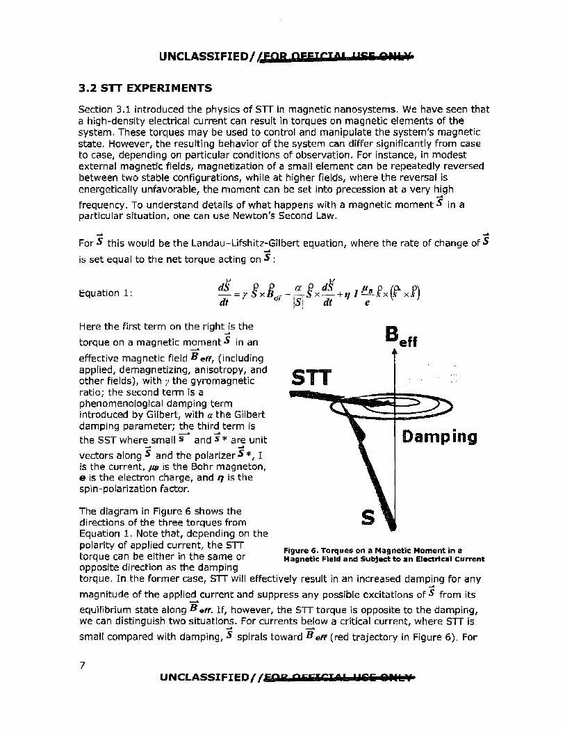
Section 3.1 introduced the physics of STT in magnetic nanosystems. We have seen that a high-density electrical current can result in torques on magnetic elements of the system. These torques may be used to control and manipulate the system's magnetic state. However, the resulting behavior of the system can differ significantly from case to case, depending on particular conditions of observation. For instance, in modest external magnetic fields, magnetization of a small element can be repeatedly reversed between two stable configurations, while at higher fields, where the reversal is energetically unfavorable, the moment can be set into precession at a very high ..... frequency. To understand details of what happens with a magnetic moment S in a particular situation, one can use Newton's Second Law.
..... ..... For S this would be the Landau-Lifshitz-Gilbert equation, where the rate of change of S ..... is set equal to the net torque acting on S:
Equation 1: dS _ . P P a P dS µ 8 o (°"' o) --ySxB 11 --
11
sx-+ql-.tx.t x.t dt ~ S dt e
Bett
STT
Here the first term on the right_!s the
torque on a magnetic m~ent S in an
effective magnetic field B eff, (including applied, demagnetizing, anisotropy, and other fields), with i' the gyromagnetic ratio; the second term is a phenomenological damping term introduced by Gilbert, with a the Gilbert damping parameter; the third term is
__. ..... the SST where small s and s * are unit Damping ... ... vectors along S and the polarizer S *, I is the current, µsis the Bohr magneton, e is the electron charge, and q is the spin-polarization factor.
The diagram in Figure 6 shows the directions of the three torques from Equation 1. Note that, depending on the polarity of applied current, the STT torque can be either in the same or opposite direction as the damping
Figure 6. Torques on a Magnetic Moment in a Magnetic Field and Subject to an Electrical Current
torque. In the former case, STT will effectively result in an increased damping for any -"
magnitude of the applie~ current and suppress any possible excitations of S from its
equilibrium state along B eff. If, however, the STT torque is opposite to the damping, we can distinguish two situations. For currents below a critical current, where STT is ..... __.,
small compared with damping, S spirals toward B eff (red trajectory in Figure 6). For
7 UNCLASSIFIED/ /FOR OEFICIPL :r&c 8fll!:Y

UNCLASSIFIEDhCFOP OFFICIO! 1155 Pt!! X
...... currents larger than the critical current, STT exceeds the damping torque and causes S -to spiral away from B eff, with a steadily increasing pr,:cession a~le. The ultimate
result can be either stable steady-state precession of S around Be" (black trajectory in .... -
Figure 6) or magnetic reversal of S into a state antiparallel to B eff, depending on the angular dependence of STT and damping torques.
Almost all experimental observations of STT rely on the GMR phenomenon to detect the current-induced reorientation of magnetic moments in nanodevices. Typical measurements include ( 1) measuring static device resistance R=V/I as a function of
...... -applied de bias current I in an applied magnetic field B and (2) measuring R versus B at a constant I. Figure 3 shows how the differential resistance dV/dI of a Cu point contact to Co/Cu magnetic multilayer varies with the bias voltage V (equivalent to I) applied across the contact. Here the multilayer magnetic moments are saturated out of the plane of the layers by a sufficiently large external magnetic field (B ~ 2T). The onset of STT-driven magnetic precession is revealed by a peak in differential resistance of the contact. The peak in dV/dI indicates the transition into precession is a reversible process, and in a small range of currents, one can continuously increase or decrease the angle of precession. However, other scenarios are also possible-for example, fast transitions between static and steady-state precession states with current-dependent dwell time.
If the applied magnetic field is small, the magnetic system can have more than one low-energy state. In the simple case of a ff 8. magnetic element with uniaxial ._. anisotropy, STT can trigger a transition between two static states that are energetically favorable. An example of such behavior is shown in Figure 7. Here the current is driven across a trilayer Py2Dnm/Cu12nm/Py4.Snm spin-valve structure patterned by electron beam
=o 8. ....._, > "'O 8.
2
1
0
.. -
--- • --- . -0.4 -0.2 0.0 0.2 0.4
I (rrA)
'
lithography into a nanopillar with a 40 x 120 nm2 cross-sectional area (Reference 48). The differential resistance of the nanopillar exhibits a hysteresis as a function of an applied bias current as the magnetization of the thin (free) permalloy (Py) layer is aligned parallel and
Figure 7. Spin-torque-driven magnetic switching for a Py20nm/Cu12nm/Py4.Snm spin valve with a 40x120-nm2 cross-sectional area, as the magnetization of the thin (free) magnetic layer is aligned parallel and antiparallel to the thicker magnetic layer by an applied current. (Reference 48)
antiparallel to the thick (hard) Py layer by the current.
The two examples presented above (Figures 3 and 7) demonstrate how simple de resistance measurements can be used for STT observation. Here the measured resistance of a device provides indirect information about the relative orientation of magnetic elements in the device. However, measured critical currents highlighted by sharp variations in the resistance remain the only experimental information that can be used to quantitatively compare theory and experiment. Moreover, the de measurements in Figure 3 provide no information about fast evolution of magnetization in the device
8 UNCLASSIFIED/ (SOR OFFIGIOI 11€6 Pt!! X •
UNCLASSIFIED/ (FOR OFFJCIIP 1155 Ot!P Y :
associated with high-frequency precession of magnetic moments. High-frequency techniques must be employed to provide such capabilities, as discussed next.
The first experiment providing unequivocal evidence that a de electrical current can result in high-frequency (tens of GHz) precession of magnetic moments was reported by Tsoi et al. in (Reference 9). Here an STT device-point contact-was placed in a microwave cavity of a high-frequency, high-field electron spin resonance (ESR) spectrometer. This arrangement allowed performing de transport experiments, such as those described above, while the contact was irradiated with high-frequency microwaves. When the frequency of external microwaves matched the precession frequency excited by the de current, an additional (rectified) voltage was detected across the contact. By detecting this voltage while varying the external frequency, field, and applied current, Tsoi et al. (Reference 9) were able to map the frequency excited by de current as a function of applied field and current. In a more recent experiment, Rippard et al. (Reference 49) fed microwaves to a point contact via electrical leads and reported observation of a similar de response.
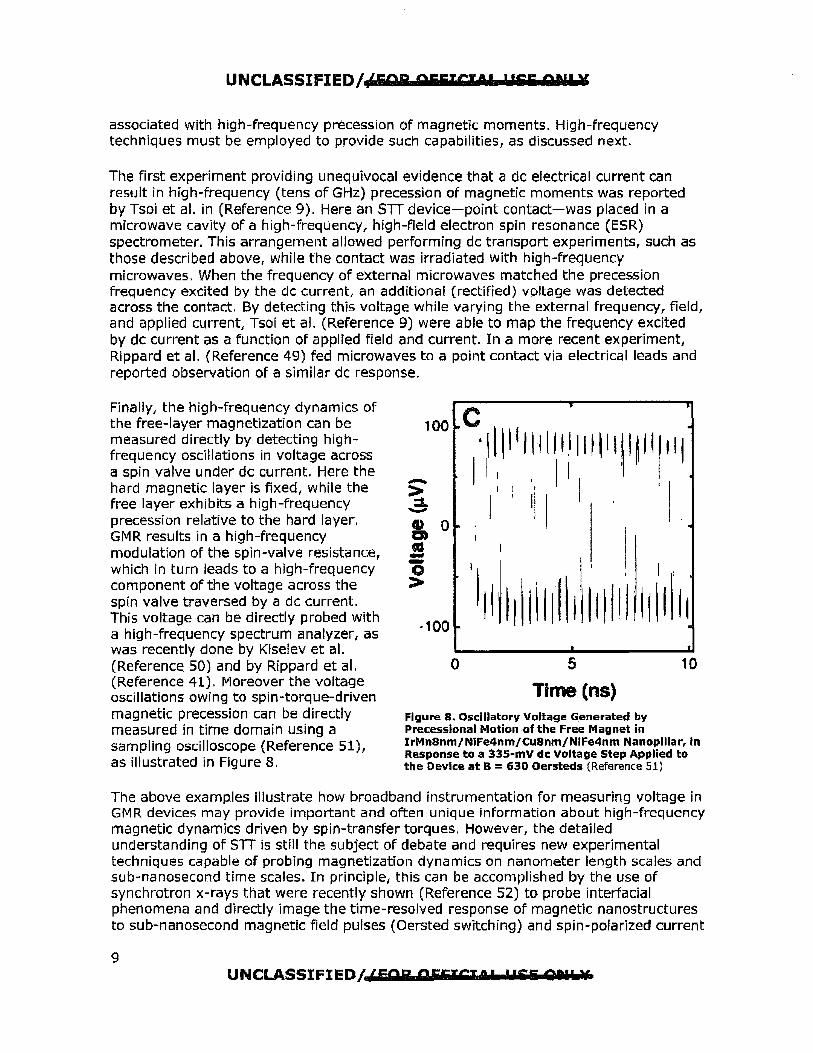
Finally, the high-frequency dynamics of the free-layer magnetization can be measured directly by detecting highfrequency oscillations in voltage across a spin valve under de current. Here the hard magnetic layer is fixed, while the free layer exhibits a high-frequency precession relative to the hard layer. GMR results in a high-frequency modulation of the spin-valve resistance, which in turn leads to a high-frequency component of the voltage across the spin valve traversed by a de current. This voltage can be directly probed with a high-frequency spectrum analyzer, as was recently done by Kiselev et al. (Reference SO) and by Rippard et al. (Reference 41). Moreover the voltage oscillations owing to spin-torque-driven magnetic precession can be directly measured in time domain using a sampling oscilloscope {Reference 51), as illustrated in Figure 8.
100
-> ::s. ........ CD 0 a,
• .., -0 >
·100
0 s Time (ns)
10
Figure 8. Oscillatory Voltage Generated by Precessional Motion of the Free Magnet in IrMn8nm/NlFe4nm/Cu8nm/NiFe4nm Nanoplllar, in Response to a 335-mV de Voltage Step Applied to the Device at B = 630 Oersteds (Reference 51)
The above examples illustrate how broadband instrumentation for measuring voltage in GMR devices may provide important and often unique information about high-frequency magnetic dynamics driven by spin-transfer torques. However, the detailed understanding of STT is still the subject of debate and requires new experimental techniques capable of probing magnetization dynamics on nanometer length scales and sub-nanosecond time scales. In principle, this can be accomplished by the use of synchrotron x-rays that were recently shown (Reference 52) to probe interfacial phenomena and directly image the time-resolved response of magnetic nanostructures to sub-nanosecond magnetic field pulses (Oersted switching) and spin-polarized current
9 UNCLASSIFIED/. (FOR OFFICJC, u55 e,1b¥

UNCLASSIFIED//509 OEFHil S.b Wlili 8HL3f
pulses (STT switching). Figure 9 shows scanning transmission x-ray microscopy (Reference 53) images of in-plane components of magnetization M - Mx in panel (a) and My in panel (b}-in the free CoFe layer (indicated by blue ellipse) of a 100x150-nm2
magnetic nanopillar. The images were obtained by scanning a focused (diameter ~ 30 nm) circularly polarized x-ray beam across the CoFe layer, with the photon energy tuned to the characteristic Co L3 resonance to provide magnetic contrast through the xray magnetic circular dichroism effect (Reference 54), and by monitoring transmission of the x-rays as a function of the position x, y with a fast avalanche detector. The Mvector field of the free layer can be reconstructed from the measured Mx and Mv components as illustrated in Figure 9c, and the ultrafast x-ray microscopy technique provided a means to monitor this field as a function of time with ~100-picosond resolution. The spatial resolution of the technique is set by the spot size of the x-ray beam ( ~30 nm) and currently limits its application to spintronic devices > 100 nm in size (Reference 52). Potentially, however, technical development of the ultrafast.x-ray microscopy may lead to an ultimate technique for STT studies that can probe the Mvector field on the nanometer length scale with picosecond time resolution.
(a) (b) (c) Figure 9. Scanning transmission x-ray microscopy images of Mx (a) and Mv (b) components of magnetization M combine into the vector field (c}, which represents the direction of Min the plane of the Cofe free layer. (Reference 52)
3.3 STT APPLICATIONS
The STT method to manipulate magnetic moments by an electrical current offers unprecedented spatial and temporal control of spin distributions and attracts considerable attention because of its potential application in a broad range of technologies. The perspective of STT for GHz communication applications and in magnetic recording technology is discussed.
The STT application in high-frequency technologies is based on the spin-transferinduced precession of spins. The previous section discussed how precession of magnetization in GMR devices can convert a de current input into an ac voltage output. The frequency of this output can be tuned from a few GHz to > 100 GHz by changing the applied magnetic field and/or the de current, effectively resulting in a currentcontrolled oscillator for use in practical microwave circuits. Hence, the STT effett in
10 UNCLASSIFIED/;GFQA Qffi&la\L W&& a•lb>f

UNCLASSIFIED/s'POR 8FFI611sk Wii!E GtlL¥
GMR structures provides a means to engineer a nanoscale high-frequency oscillator powered and tuned by de current. Such an oscillator could have frequency characteristics spanning more than 100 GHz and perhaps into terahertz range. Linewidths as narrow as 2 megahertz were demonstrated (Reference 55), leading to quality factors over 18,000. Potential applications for such high-frequency sources include integrated transceivers for wireless and wired applications, as well as wireless and wired chip-to-chip and on-chip communications. For the latter, logic circuits with a spin wave bus were proposed (Reference 56, 57) as an interface between electronic circuits and integrated spintronics circuits. Here spin waves are used for information transmission and processing, and the STT effect can provide a means for efficient spinwave generation on the nanoscale.
In high-speed, high-density magnetic recording technology, STT could replace the Oersted field currently used for writing magnetic bits in storage media (for example, magnetic random access memory [MRAM]), thus leading to smaller and faster magnetic memory. Figure l0a schematically shows a bit cell of a conventional MRAM. The bit state is programmed to a 1\1" or '\0 11 by switching between the parallel and antiparallel states of a GMR-like storage element. The first-generation M RAM utilizes magnetic tunnel junctions (MTJ) as storage elements because of their higher magnetoresistance ratios and impedance-matching constraints. However in scaling MRAM to small dimensions, the same constraints are expected to drive a transition from MTJs to fully metallic spin-valve storage elements. The switching between \\1" and \'011 states (writing) relies on magnetic reversal of the MTJ's free layer, achieved by passing electrical currents down the "bit" and "write" lines, that generates a sufficiently strong magnetic field at their intersection (that is, for a given MTJ). However, as the spatial decay of this Oersted field is rather slow ( ~l/r2), it may affect neighboring cells. This makes scaling of MRAM to small dimensions questionable.
(a)
Bypass Line
--+;.' ~nding . ~ ~d ..
Source Drain
Si substrate
Write Word Line
(b)
Source
MTJ ~
•-/•· Drain
Si substrate
Figure 10. Conventional MRAM Cell (a) Versus STT MRAM Cell {b) (Reference 58)
STT MRAM (see Figure 10b) removes the constraints on scalability. Here the switching of the free layer magnetic moment is achieved by SIT switching when a high-density electrical current is driven directly through the storage element (MTJ or spin valve). This writing is thus performed at high current levels, while the reading (measuring the resistance of the element) is done at low currents. Since STT MRAM eliminates the need for "write" and "bypass11 lines, a more compact memory can be realized.
11 UNCLASSIFIED/ (EAR OFFICIO! 1 PSS Ot!J Y

UNCLASSIFIED/;SFtUl ilFFi&ICk !!Iii SUik¥
3.4 STT·DRIVEN MOTION OF MAGNETIC DOMAIN WALLS
Yet another manifestation of STT in metallic ferromagnets is a motion of magnetic domain walls traversed by an electrical current. The original prediction of the effect dates back to 1978, when Luc Berger predicted that a spin-polarized current should apply a torque to a magnetic domain wall (Reference 59), In a series of remarkable but only recently appreciated works, Berger set the theoretical (Reference 59-62) and experimental (Reference 63-65) groundwork for current-induced domain wall motion (CIDWM), which is now documented in materials ranging from magnetic semiconductors (Reference 66} to perpendicular-anisotropy superlattices (Reference 67). But the most widely studied materials by far have been metallic ferromagnets (Reference 10, 11, 68-82), including Py (Ni31Fe19), CoFe, and Co, because of their decades-long ubiquity in magnetic storage technology.
The CIDWM effect can be qualitatively understood on the basis of the following arguments. Consider an electrical current flowing between two magnetic domains (A and B) with opposite magnetizations and, thus, traversing a 180-degree magnetic domain wall. The situation is similar to that of a single N/F interface discussed in Section 3.1. While in domain A, spins of conduction electrons are preferentially aligned with the magnetic moment of A. Once into domain B, the spins reverse to align with the moment of B. In reversing the electron spins, magnetic moments in the domain wall experience a torque associated with the change in angular momentum that occurs from the rotation of electrons spins. This spin-transfer torque can move the domain wall in the direction of the electron flow.
Moving magnetic domain walls with current was proposed as the basis for a new type of magnetic memory called "racetrack" (Reference 83). In contrast to today's hard disk drives (HDD), which rely on spinning motion of a disk to move their magnetic regions where the data is stored past a read head, the racetrack memory exploits the idea of moving magnetically stored data electronically. Figure 11 illustrates the concept of the racetrack. The racetrack is a ferromagnetic nanowire, with data encoded as a pattern of magnetic domains along the wire. Current pulses can move the entire pattern along the wire. The two cartoons of Figure lla
A B"' _J:
C J-1_ _-; ..
~-V\ri:mg
D :,_I
/. vor11c:,11 wcctracK Hacatracf..
slor:tgc mr:J.'f
Figure 11. Racetrack Memory Concept. (Reference 83)
show the domain wall patterns in the racetrack before and after they have moved past read and write elements. Reading is achieved by measuring the resistance of a tunnel junction element connected to the racetrack (Figure llb}; writing (Figure 11c), by applying local magnetic fields-for example, the fringing fields of a domain wall moved in another nanowire. If Li-shaped nanowires are placed normal to the plane of a chip and arranged into high-density arrays of racetracks (Figure 11d), the resulting storage density can be higher than that in solid-state memory devices like flash RAM and
12 UNCLASSIFIED/ /FOR Qlilil&I r.la Yii 8HL I
UNCLASSIFIED//f&II &FFIOIAI! USI 8HL'f
similar to conventional HDDs; but the racetrack memory would have much higher read/write performance than HOD.
4. Antiferromagnetic Metal Spintronics
Recently, MacDonald and coworkers (Reference 84) predicted that effects similar to GMR and STT observed with ferromagnets ought to occur in multilayer systems where the ferromagnetic (F) components are replaced by antiferromagnets (AFM). First, they predicted that the resistance of an AFM spin valve-where two AFM layers are separated by an N spacer-could depend on the relative orientations of the magnetic moments in the two AFM layers (antiferromagnetic GMR = AGMR). Second, they predicted that injecting a sufficiently strong current density into an AFM should affect its magnetic state via current-induced spin torque. These new AFM effects could lead to new all-AFM spintronics where AFMs are used in place of Fs.
Replacing F metals with AFM metals in a spintronic device has several advantages. While AGMR of an AFM spin valve was predicted (Reference 84) to be similar in magnitude to GMR in standard F spin valves, the critical current needed to alter the magnetic order in AFMs can be smaller than for Fs, partly because spin torques can act through the entire AFM volume. The estimate of the necessary current density j ~ 109
A/m2 (Reference 84) was less than the typical j ~ 1011 A/m2 needed to reverse the magnetic order in F/N/F multilayers (Reference 5-9, 40-43, 48-51). Finally, using AFM metals in spintronic devices in place of F metals would eliminate unwanted effects of shape anisotropy on the magnetic stability of small elements, thus potentially offering better control of the magnetic state in nanoscale systems and easing fabrication requirements.
Following the original predictions of MacDonald and coworkers (Reference 84), Xu et al. (Reference 85) calculated the AGMR for a simple AFM/N/AFM/N = FeMn/Cu/FeMn/Cu multilayer, and Gomonay and Loktev (Reference 86) provided additional theoretical evidence that polarized current can destabilize the equilibrium state of an AFM. Note, however, that all calculations to date are for perfect samples and depend on quantum coherence. It is known that disorder can reduce the predicted effects. Experiments are thus crucial to see if any such effects are visible in real samples.
4.1 ANTIFERROMAGNETIC GMR
To the author's knowledge 1 the only experimental study searching for AGMR was performed by Wei et al. (Reference 87). They have measured current-in-plane (CIP) and current-perpendicular-to-plane (CPP) magnetoresistances (MR) of magnetic multilayers containing two antiferromagnetic layers separated by a nonmagnetic layer. Such an antiferromagnetic spin valve, AFM/N/AFM, was predicted (Reference 84) to exhibit AGMR similar to GMR seen in ferromagnetic spin valves, F/N/F, containing two ferromagnetic layers separated by a nonmagnetic layer. Note, however, that calculations (Reference 84) assumed ballistic transport in samples with perfect layers and interfaces where AGMR is a consequence of quantum interference effects. Thus, any disorder that produces diffusive scattering and weakens quantum interference will weaken any such AGMR.
13 UNCLASSIFIED/ (502 OEEIGICL 'li"lii Qella¥ •

UNCLASSIFIED/ ,'FOR: &ffi&ll&I: 1181 IHI:¥
In F/N/F trilayers, the relative orientation of the magnetizations of the two Fs is controlled by an externally applied magnetic field B. To achieve well-defined antiparallel and parallel states of the two F layers, the moment of one F is often \~pinned," via exchange coupling (exchange bias) to an adjacent AFM layer (Reference 88, 89), leaving the moment of the other free to reverse in much smaller B. In a simple AFM/N/ AFM sample, just applying a field B is not expected to be efficient because of the weak effect of external fields on magnetic moments in AFMs. To achieve better control of the AFMs, AFM/N/AFM spin valves can be sandwiched between two Flayers to give F/AFM/N/AFM/F, with the two AFM layers differently exchange-coupled to their respective F neighbors. Applying a magnetic field to change the magnetic order of the F layers should then also affect the order of the AFM layers. In addition to AFM/N/AFM and F/AFM/N/AFM/F multilayers, Wei et al. (Reference 87) have studied a variety of structures-F/AFM/N/AFM, AFM/F/N/AFM, F/AFM, and single F and AFM layers-to isolate the MR observations of interest from potential spurious effects.
For small applied currents, neither standard current-in-plane (CIP) MR measurements on extended multilayer films nor CPP MR measurements with point contacts showed any MRs for samples of all types. For larger applied currents, small positive CPP MRs (resistance is highest at saturation) were sometimes observed in samples with at least one Flayer, while no MR was seen in samples with no Fs. These observations suggest sputtered AFM/N/AFM multilayers do not show AGMR, possibly owing to mostly diffusive transport in such imperfect films. Small MRs observed at higher currents in films with F layers may be associated with the suppression at high currents of spin accumulation induced within and around Fs (Reference 90). Further studies on high-quality films are still needed to verify any possible existence of AGMR in such structures.
4.2 ANTIFERROMAGNETIC STT
Stimulated by the theoretical studies in (Reference 84-86), four experimental searches for effects of STT on AFMs have been published so far (Reference 91-94), all working with exchange-biased spin-valves (EBSVs) of the form AFM/Fl/N/F2. Here the AFM lies outside the \\active" GMR region of the two F layers and serves mainly to "pin" the magnetization of the adjacent F2 layer to a higher reversing (switching) field than that of the "free" Fl layer, leaving the Fl layer free to rotate at a lower field. The pinning is produced either by heating the sample to above the blocking temperature of the AFM, applying a magnetic field, and then cooling to room temperature with the field on or by applying a magnetic field during sample growth. Wei et al. (Reference 91) used a point contact to inject a high de current density j ,.... 1012 A/m2 approximately CPP into an EBSV film. Urazhdin and Anthony (Reference 92) sent a de CPP current density j ~ 5 x 10¹¹ A/m 2 into electron-beam-lithography-fabricated nanopillar EBSVs. Tang et al. (Reference 93) sent a de current-in-plane (CIP) current density ~ 1010 Nm2 into an EBSV film with a metallic AFM. Dai et al. (Reference 94) sent an ac CIP current density j ~ 109 A/m2 into an EBSV film with an insulating AFM. In all of the studies (Reference 91-94), it was found that a sufficiently high bias current can influence the magnetic reversal of the \\pinned" Fl layer. As the pinning {exchange bias) is known to be associated with interfacial AFM moments (Reference 88, 89)i this observation can be taken as evidence of effects of the current on the AFM predicted in (Reference 84-86), given that other spurious effects (for example, Joule heating} can be ruled out.
14 UNCLASSIFIED/ (FOB OEEICJ0 1 , •55 Ollb¥
UNCLASSIFIED/ (EAR O&FICIIP PflliiE f.HU!V
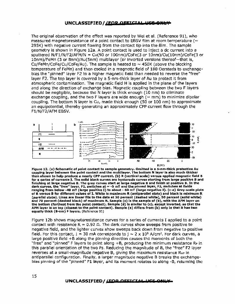
The original observation of the effect was reported by Wei et al. (Reference 91), who measured magnetoresistance of a point contact to EBSV film at room temperature ( ~ 295K) with negative current flowing from the contact tip into the film. The sample geometry is shown in Figure 12a. A point contact is used to inject a de current into a sputtered N/F1/N/F2/AFM/N = Cu(SO or 100nm)/CoFe(3 or 10nm)/Cu(lOnm)/CoFe(3 or lOnm)/FeMn (3 or Snm)/Au(Snm) multilayer (or inverted versions thereof-that is, Cu/FeMn/CoFe/Cu/CoFe/Au). The sample is heated to N 450K (above the blocking temperature of FeMn) and then cooled in a magnetic field of 180 Oersteds to exchangebias the "pinned" layer F2 to a higher magnetic field than needed to reverse the "free" layer F2. The top layer is covered by a 5-nm-thick layer of Au to protect it from atmospheric contamination. The magnetic field H is applied in the plane of the layers and along the direction of exchange bias. Magnetic coupling between the two F layers should be negligible, because the N layer is thick enough (10 nm) to eliminate exchange coupling, and the two Flayers are wide enough ( ~ mm) to minimize dipolar coupling. The bottom N layer is Cu, made thick enough (SO or 100 nm) to approximate an equipotential, thereby generating an approximately CPP current flow through the F1/N/F2/AFM EBSV.
a l F1
N
F2
IFM
N
j J --
_,. ......... ._ ... -- e
·60
, ., ;
I ,
.40
B(mH
-20 ~
30
0
-30
I!) ;f 0 §.. ·!O -20
0
-20
Figure 12. (a} Schematic of point contact to sample geometry. Omitted is a 5-nm-thick protective Au capping layer between the point contact and the multilayer. The bottom N layer is also much thicker than shown to help produce a nearly CPP current. (b) R (vertical scale) versus applied magnetic field B for a series of currents I. The solld black curves are hysteresis curves starting from large positive Band finishing at large negative B. The grey curves start at large negative B and finish at positive B. In the dark curves, the "free" layer, Fl, switches at ,v ·5 mT and the pinned layer, F2, switches at fields ranging from below -40 mT (large positive I) ta about - 60 mT (large negative I). (c-e) Grey-scale plots of R versus B for different values of I. White is maximum R (antiparallel state) and black is minimum R (parallel state). Lines are linear fits to the data at 30 percent (dashed white), 50 percent (solid white) and 70 percent (dashed black) of maximum R. Sample (c) is the sample of (b), with the AFM layer on the bottom (furthest from the point contact}. Sample {d} is similar to (c), except inverted, so that the AFM layer is on top (closest to the point contact). Sample (e} differs from (b) only in that it has two equally thick (B•nm) Flayers. (Reference 91)
Figure 12b shows magnetoresistance curves for a series of currents I applied to a point contact with resistance R = 0.92 n.. The dark curves show sweeps from positive to negative field, and the lighter curves show sweeps back down from negative to positive field. For this contact, I = 30 mA corresponds to j ~ 2 x 10⁸ A/cm2• For dark curves, a large positive field +B along the pinning direction causes the moments of both the "free" and "pinned" F layers to point along +B, producing the minimum resistance RP in this parallel orientation of the two Fs. Reducing the magnitude of B, the "free" F2 layer reverses at a small-magnitude negative B, giving the maximum resistance RAP in antiparallel configuration. Finally, a larger magnitude negative B breaks the exchangebias pinning of the "pinned" Fl layer, and its moment rotates to along -B, returning the
15 UNCLASSIFIED/ (FOR OFEICIOI 1165 QIII )(
UNCLASSIFIED/ ,'FQA Qfflfiillk HEE 8PIL¥
sample to RP, For lighter curves of back-sweeps (Figure 12b}, the measured resistance follows these changes in reverse order.
Focusing on the dark curves, we see that the switching field of the free layer Fl is essentially independent of the magnitude of I and shows little broadening. In contrast, the switching field of the pinned layer F2 broadens significantly as the magnitude of I increases, and the midpoint of the switching also shifts with I, increasing for - I and decreasing for + I. Similar behaviors are seen also in the lighter curves. Opposite shifts for + I and - I indicate these shifts cannot be due to Joule heating, which should cause shifts in the same direction for both directions of I. But Joule heating might contribute to the broadening of the switching transitions. The shifts of the dark curves are specified more clearly in Figure 12c, which shows grey-scale plots of the heights of the curves in Figure 12b, with white representing the antiparallel state of maximum resistance, and black the parallel state of minimum resistance. Data for three representative contacts (out of 29) on three different samples show that the behavior of interest is not limited to a single sample or contact, and that similar results are generally obtained for straight line fits to 30 percent (white dashed lines), SO percent (solid white lines), and 70 percent (solid black lines) of the maximum change in R. The sample in Figure 12d is a contact with R = 1.6 n to an inverted version of the sample in Figures 12b and c, so that the \'directions" of currents are reversed. The sample in Figure 12e has equal thickness Fl ;;;;; F2 ;;;;; 3-nm layers. All three samples show the same features-that is, electrons passing through F2 into the AFM layer enhance pinning, and electrons passing through the AFM layer into F2 reduce it. Similar to the case of AFM=CoFe, a negative current density ~1012 A/m2 injected through the F=CoFe into an AFM=IrMn/CoFe interface (Reference 95, 96) was found to increase the exchange bias, while a positive current decreased it.
Wei et al. (Reference 91) proposed the following qualitative explanation for these asymmetric changes in switching (exchange bias) field with current. Near the switching field, the metastability of F2's opposite to field orientation is due almost entirely to exchange interactions with uncompensated moments in the surface layer of the antiferromagnet. Some of these spins are pinned, thereby inducing an energy barrier for ferromagnetic layer spin reversal (Reference 88, 89). Electrons flowing from F2 into AFM induce torques on moments in the AFM matrix, altering its magnetic configuration (Reference 84). These STT torques tend to favor parallel alignment of moments at the F2/AFM interface and will therefore tend to increase the exchange bias field. Electrons flowing in the opposite direction will tend to have the opposite effect. The observed variations in exchange bias mediated by an electrical current thus can be taken as good evidence of the STT effect in AFM. However, such transport measurements do not distinguish between effects of the current on the bulk AFM and those on interfacial AFM moments, and more elaborate techniques are needed to obtain a detailed understanding of the phenomenon.
5. Summary and Conclusions
The semiconductor industry has distinguished itself by a long-term trend known as Moore's law (Reference 97) that foresees an exponential increase in transistor density on a chip, doubling approximately every 2 years. Continuing at this pace, the transistor density will reach ~ 1013 cm-2 by 2035, which at clock speeds of ~10 GHz would result in "'40 MW/cm2 of power dissipated on a chip. Unless the energy dissipation from
16 UNCLASSIFIED/ ;reftt 8PPlllf1k VIE Gt11 ¥

UNCLASSIFIED/ .,r:aa QFFJiQI I k I H,E Qllklf
transistor switching can be reduced dramatically, the thermal load associated with 40 MW/cm2 will exceed that in a rocket nozzle. The failure of thermal management on a chip might end the continued progress of the semiconductor industry well before 2035. The International Technology Roadmap for Semiconductors (http://www.itrs.net) has termed this imminent collapse the "Red Brick Wall," where \'Red 11 indicates no "known manufacturable solutions" (of reasonable confidence) exist for continued scaling in some aspect of the semiconductor technology.
The scenario above motivates the search for signal-processing devices that dissipate very little energy when they switch. The emerging spintronic technology might offer such devices where information is carried by spin-in contrast to CMOS transistors, where it is carried by charge-since spin has an inherent advantage over charge when it comes to energy dissipation. Therefore, if a reliable way can be found to control and manipulate spins, spintronic devices could offer higher data processing speeds, lower electricity consumption, and many other advantages over conventional chips, perhaps including the ability to carry out radically new quantum computations.
A spintronic device calls for efficient methods to generate, conduct, process/ and detect spin-encoded signals. We have reviewed the physics and emerging applications of two principal spintronic phenomena-giant magnetoresistance and spin-transfer-torquethat provide means to detect (GMR) and manipulate (STT) the spin signals. GMR has already spawned major technological change in the information storage industry with the usage of GMR sensors and read heads and, along with tunneling magnetoresistance (TMR), is expected to continue to dominate the detection of spin-encoded signals. STT is a more recent development in spintronics that provides an efficient means of controlling and manipulating spin distributions on the nanometer length scale and the picosecond-time scale, thus positioning STT as the method of choice for fast processing of spin signals in nanodevices.
What is the future of spintronic applications? A number of new spintronic devices based on GMR and STT have been proposed. These include high-frequency (GHz) oscillators, sources, and detectors, as well as magnetic field sensors-for example, in nonvolatile memories such as racetrack and STT magnetic random access memory (STT-MRAM). However, much fundamental work remains to be done before we see commercial applications of these devices. For the memory industry, development of these spintronic applications may lead to a universal memory that would combine cost benefits of DRAM, speed of SRAM, and nonvolatility of flash RAM. Potentially all logic operations on a chip could be carried out by manipulating spins in metallic systems instead of manipulating charges in semiconductor transistors, as in conventional microchips. Moreover, such operations could be combined on a chip with a universal memory. This would result in a new scalable and radiation-resistant electronics, computers, and so forth. The radiation resistance would be of particular interest for aerospace applications because the radiation in space is known to severely damage conventional electronics by building up a destructive charge in transistors. Long space trips that would expose onboard electronics to years of radiation would benefit from the radiation resistance and reduced power consumption (for example, like a nonvolatile memory that can retain the stored information even when not powered) of metallic spintronic devices. More generally, the impact of reduced power consumption in electronic devices is hard to overestimate, as we rely on such devices in almost every aspect of our everyday lives.
17 UNCLASSIFIED/ ,Sliii8R 8ffHilAI: lj!J!! Slit: I'

UNCLASSIFIED/ (FOR OFFIGI O L Wli& 8Hl!:Y
Finally, metallic spintronics and its applications discussed in this report are all based on already well-established physical phenomena such as GMR and STT. As the spintronics field is still in a relative state of infancy, new and more exciting phenomena are likely to be uncovered in the future.
6. References
(1) Baibich 1 M. N., et al., Phys. Rev. Lett. 61, 2472 (1988).
(2) Binasch, G., et al., Phys. Rev. B 39, 4828 (1989).
(3) Slonczewski, J. C., J. Magn. Magn. Mater. 159, Ll (1996).
(4) Berger, L., J. Appl. Phys. 81, 4880 (1997).
(5) Tsoi, M., et al., Phys. Rev. Lett. 80, 4281 (1998).
(6) Myers, E. B., et al., Science 285, 867 (1999).
(7) Sun, J. Z., J. Magn. Magn. Mater. 202, 157 (1999).
(8) Wegrowe, J.-E., et al., Europhys. Lett. 45, 626 (1999).
(9) Tsoi, M., et al., Nature 406, 46 (2000).
(10) Beach, G. S. D., et al., Phys. Rev. Lett. 97, 057203 (2006).
(11) Beach, G. 5. D., et al., Phys. Rev. Lett. 102, 067201 (2009).
(12) Fert, A., Bruno, P., in Ultrathin Magnetic structures II: An Introduction to the Electronic, Magnetic and Structural Properties, ed. by J.A.C. Bland and B. Heinrich (Berlin: Springer, 1994 )1 p.82.
(13) Levy, P. M., in Solid State Physics, ed. by H. Ehrenreich and D. Turnbull, vol. 47 (Boston, London: Acad. Press, 1994), p.367.
(14) Dieny, B., J. Magn. Mag. Mat. 136, 335 (1994).
(15) Gijs, M. A.M., Bauer, G. E.W., Adv. Phys. 46, 285 (1997).
(16) Ansermet, J.-Ph., J. Phys.: Cond. Mat. 10, 6027 (1998}.
(17) Bass, J., Pratt, w. P., Jr., J. Magn. Magn. Mat. 200, 274 (1999).
(18) Fert, A., Piraux, L., J. Magn. Magn. Mat. 200, 338 (1999).
(19) Gijs, M. A.M., in Magnetic Multilayers and Giant Magnetoresistance: Fundamentals and Industrial Applications, ed. by U. Hartmann (Berlin: Springer, 2000), p.130.
18 UNCLASSIFIED/ (FOP QFEICI0k lllii IJHtY

UNCLASSIFIED/71P81'l 9PPI81Jlal: WII I.Hlbl.f
(20) Coehoorn, P., in Magnetic Multilayers and Giant Magnetoresistance: Fundamentals and Industrial Applications, ed. by U. Hartmann (Berlin: Springer, 2000), p.65.
(21) Barthelemy, A., Fert A., and Petroff, F., in Handbook of Magnetic Materials, edited by K. H.J. Buschow (Amsterdam: Elsevier, 1999), p.1.
(22) Tsymbal, E.Y., Pettifor, D.G., in Solid State Physics, ed. by H. Ehrenreich and F. Spaepen, Vol. 56 (Academic Press, 2001) pp.113-237.
(23) Ashcroft, W., Mermin, D., Solid State Physics (Saunders College Publishing, Forth Worth, 1976).
(24) Ciureanu, P., in Thin Film Resistance Sensors, ed. by P. Ciureanu, S. Middelhoek (Institute of Physics Publishing, Bristol, 1992), p. 253.
(25) Electrocrystallization, ed. by R. Weil, R. G. Barradas (The Electrochemical Society, Pennington, 1981).
(26) Lashmore, D.S., Dariel, M. P., J. Electrochem. Soc. 135, 1218 (1988).
(27) Ohring, M., The Materials Science of Thin Films (Academic, Boston, 1992).
(28) Slaughter, J. M., Pratt, W. P., Jr., and Schroeder, P.A., Rev. Sci. Instrum. 60, 127 (1989).
(29) Parkin, S.S. P., More1 N. 1 and Roche, K. P., Phys. Rev. Lett. 64, 2304 (1990).
(30) Parkin, S.S. P., Bhadra, R., and Roche, K. P., Phys. Rev. Lett. 66, 2152 (1991).
(31) Fert, A., Campbell, I. A., J. de Physique 32, Cl-46 (1971).
(32) Mott, N. F., Proc. Roy. Soc. London, Ser. A 153, 699 (1936), and 156, 368 (1936), and Adv. Phys. 13, 325 (1964),
(33) Pratt, W. P., Jr., et al., Phys. Rev. Lett. 66, 3060 (1991).
(34) Dieny, B., et al. J. Appl. Phys. 69, 4774 (1991).
(35) Piraux, L., et al., Appl. Phys. Lett. 65, 2484 (1994).
(36) Blondel, A., Meier, J. P., Doudin, B., Ansermet, J.-Ph., Appl. Phys. Lett. 65, 3019 (1994).
(37) Tsoi1 M., Jansen, A. G. M.1 Bass, J., J. Appl. Phys. 81, 5530 (1997).
(38) Smith, C., Proc. UK Conf. for Sensors, Test and Measurement Technology, Birmingham, England, Jan. 22-23, 1997.
(39) Daughton, J. M., et al., IEEE Trans. Magn. 30, 4608 (1994).
19 UNCLASSIFIED/ .,raR 8Ffil@IAI: U8l! 8HI! a
UNCLASSIFIED/;fliOA 81iliiE61 IL I Iii& ODIL¥
(40) Ji, Y., Chien, C. L., Stiles, M. D., Phys. Rev. Lett. 90, 106601 (2003).
(41) Rippard, W. H., Pufall, M. R., Kaka, S., Russek, S. E., Silva, T. J., Phys. Rev. Lett. 92, 27201 (2004).
(42) Katine, J. A., Albert, F. J., Buhrman, R. A., Myers, E. B., Ralph, D. C., Phys. Rev. Lett. 84, 3149 (2000).
(43) Grollier, J., et al., Appl. Phys. Lett. 78, 3663 (2001).
(44) Liu, Y., Zhang, Z., Wang, J., Freitas, P. P., Martins, J. L., J. Appl. Phys. 93, 8385 (2003)
(45) Mariya, R., Hamaya, K., Oiwa, A., Munekata, H., Jpn. J. Appl. Phys. Part 2 - Lett. Express Lett. 43, L825 (2004).
(46) Dieny, B., et al., Phys.Rev.B 43, 1297 (1991).
(47) Waintal, X., Myers, E. B., Brouwer, P. W., Ralph, D. C., Phys. Rev. B 62, 12317-12327 (2000)
(48) Braganca, P.M., et al., Appl. Phys. Lett. 87, 112507 (2005).
(49) Rippard, W. H., et al., Phys. Rev. Lett. 95, 067203 (2005).
(50) Kiselev, S. I., et al., Nature 425, 380 (2003).
(51) Krivorotov, I. N., et al., Science 307, 228-231 (2005).
(52) Acremann, Y., et al., Phys. Rev. Lett. 96, 217202 (2006).
(53) Kilcoyne, A. L. D., et al., J. Synchrotron Radiat. 10, 125 (2003).
(54) Stohr, J., et al., Science 259, 658 (1993).
(55) Rippard, w. H., Pufall, M. R., Kaka, s.J Silva, T. J., Russek, s. E., Phys. Rev. B 70, 100406 (2004).
(56) Khitun, A., Nikonov, D. E., Bao, M., Galatsis, K., Wang, K. L., Nanotechnology 18, 465202 (2007).
(57) Schneider, T., et al., Appl. Phys. Lett. 92, 022505 (2008).
(58) Driskill-Smith, A. A. G., Huai, Y., Future Fab Intl. 23, 28 (2007).
(59) Berger, L., J. Appl. Phys. 49, 2156 (1978).
(60) Berger, L., J. Appl. Phys. 55, 1954 (1984).
(61) Berger, L., Phys. Rev. B 33, 1572 (1986).
20 UNCLASSIFIED/ /,FOR OFFICJ0P I PSE Al!! Y
UNCLASSIFIED,) FOR OFFICIAL 891! 9Ht f
(62) Berger, L., J. Appl. Phys. 63, 1663 (1988).
(63) Freitas, P. P., Berger, L., J. Appl. Phys. 57, 1266 (1985).
(64) Hung, C.-Y., Berger, L., J. Appl. Phys. 63, 4276 (1988).
(65) Hung, C.-Y., Berger, L., Shih, C.Y., J. Appl. Phys. 67, 5941 (1990).
(66) Yaf!lanouchi, M., Chiba, D., Matsukura, F., Ohno, H., Nature 428, 539 (2004).
(67) Ravelosona, D., et al., Phys. Rev. Lett. 95, 117203 (2005).
(68) Tsoi, M., Fontana, R. E., Parkin, s. S. P., Appl. Phys. Lett. 83, 2617 (2003).
(69) Grollier, J., et al., Appl. Phys. Lett. 83, 509 (2003).
(70) Beach, G. S. D., Nistor, C., Knutson, C., Tsoi, M., Erskine, J. L., Nat. Mater. 4, 741 (2005).
(71) Beach, G. S. D., Knutson, C., Tsoi, M., Erskine, J. L., J. Magn. Magn. Mater. 310, 2038 (2007).
(72) Hayashi, M., et al., Phys. Rev. Lett. 96, 207205 (2006).
(73) Hayashf, M., et al., Nat. Phys. 3, 21 (2007).
(74) Klaui, M., et al., Appl. Phys. Lett. 83, 105 (2003}.
(75) Kimura, T., Otani, Y., Yagi, I., Tsukagoshi, K., Aoyagi, Y., J. Appl. Phys. 94, 7226 (2003).
(76) Vernier, N., Allwood, D. A., Atkinson, D., Cooke, M. D., Cowburn, R. P., Europhys. Lett. 65, 526 (2004).
(77) Laufenberg, M., et al., Phys. Rev. Lett. 97, 046602 {2006).
(78) Thomas, L., et al., Nature 443, 197 (2006).
(79) Yamaguchi, A., et al., Phys. Rev. Lett. 92, 077205 (2004).
(80) Yamaguchi, A., et al., Phys. Rev. Lett. 96, 179904 (2006).
(81) Klaui, M., et al., Phys. Rev. Lett. 95, 026601 (2005).
(82) Meier, G., et al., Phys. Rev. Lett. 98, 187202 (2007).
(83) Parkin, S. S. P., Hayashi, M., Thomas/ L., Science 320, 190 (2008).
(84) Nunez, A. S., et al., Phys. Rev. B 73, 214426 (2006).
21 UNCLASSIFIED/ (EAR OEFICIOP 1165 Q91b¥

UNCLASSIFIED/,S P8~ 8PP!CIJtt USE OiQtf
(85) Xu, Y., Wang, S., Xia, K., Phys. Rev. Lett. 100, 226602 (2008).
(86) Gomonay, H., Loktev, V., Low Temp. Phys. 34, 198 (2008).
(87) Wei, Z., Sharma, A., Bass, J., Tsoi, M., J. Appl. Phys. 105, 07D113 (2009).
(88) Meiklejohn, W. H., Bean, C. P., Phys. Rev. 102, 1413 (1956).
(89) Stohr, J., Siegmann, H. C., Magnetism: from fundamentals to nanoscale dynamics (Springer Series in Solid-State Sciences, Vol. 1521 Springer, 2006).
(90) Urazhdin, S., Chien, C. L., Guslienko, K. Y., Novozhilova, L., Phys. Rev. B 73, 054416 (2006).
(91) Wei, Z., et al., Phys. Rev. Lett. 98, 116603 (2007).
(92) Urazhdin, S., Anthony, N., Phys. Rev. Lett. 99, 046602 (2007).
(93) Tang, X.-L., Zhang, H.-W., Su, H., Zhong, 2.-Y., Jing, Y.-L., Appl. Phys. Lett. 91, 122504 (2007).
(94) Dai, N. V., et al., Phys. Rev. B 77, 132406 (2008).
(95) Basset, J., Sharma, A., Wei, Z., Bass, J., Tsai, M., Proc. SPIE 7036,. 703605 (2008).
(96) Wei, Z., Basset, J., Sharma, A., Bass, J., Tsai, M., J. Appl. Phys. 105, 07D108 (2009).
(97) Moore, G. E., Electronics Magazine (McGraw Hill, New York, 1965).
22 UNCLASSIFIED/,CFOlil :liHiiFIGII Is. WGE Otlla>f