Embed Size (px)
Citation preview

11 SERIAL PERIPHERAL INTERFACE (SPI)
Figure 11-0.
Table 11-0.
Listing 11-0.
OverviewThe ADSP-21161 is equipped with a synchronous serial peripheral inter-face port that is compatible with the industry-standard Serial Peripheral Interface (SPI). The SPI port supports communication with a variety of different peripheral devices such as CODECs, data converters, sample rate converters, S/PDIF or AES/EBU digital audio transmitters and receivers, LCDs, shift registers, microcontrollers, and FPGA devices with SPI emulation.
The processor's SPI port provide the following features and capabilities:
• A simple four wire interface consisting of two data pins, a device select pin, and a clock pin
• Full-duplex operation allowing the ADSP-21161 to transmit and receive data simultaneously on the same port
• Special data formats to accommodate little and big endian data, dif-ferent word lengths, and packing modes
• Master and slave modes as well as multi-master mode in which the ADSP-21161 can be connected to up to four other SPI devices
• Open drain outputs to avoid data contention and to support multi-master scenarios
• Programmable baud rates, clock polarities, and phases
• Slave booting from a master SPI device
ADSP-21161 SHARC DSP Hardware Reference 11-1

Overview
Functional DescriptionThe SPI interface is essentially a shift register that serially transmits and receives data synchronously with the SPI clock signal (SPICLK). Figure 11-1 on page 11-2 provides a block diagram of the ADSP-21161 SPI interface. When an SPI transfer occurs, a single shift register simulta-neously shifts transmitted data out one end of the shift register and received data into the other end of the shift register. The data is shifted into or out of the shift register on two separate pins: the Master In Slave Out (MISO) pin and the Master Out Slave In (MOSI) pin.
Figure 11-1. ADSP-21161 SPI Block Diagram
During data transfers one SPI device acts as the SPI master, controlling the data flow by generating the SPICLK and asserting the SPI device select signal (SPIDS). The other SPI device acts as the SPI slave by accepting new data from the master into it's shift register using the MOSI pin while trans-
S P I IN TE R F A C E L O G IC
M O S I M IS O S P IC L K S P ID S
S P IR XR e c e iv eR e g is te r
S P I In te rn a lC lo c kG e n e ra to r
3 2
D M d a ta b u sP M d a ta b u sI/ 0 d a ta b u s
M MSS S P IC TLS P IS TA T
S h if t R e g is te r
S P IT XT ra n s m itR e g is te r S P I IR Q o r
D M A R e q u e s t
F L A G x
11-2 ADSP-21161 SHARC DSP Hardware Reference

Serial Peripheral Interface (SPI)
mitting requested data out of the shift register using the MISO pin. Data to be transmitted is written to the SPI transmit register (SPITX) and then automatically transferred into the shift register. Once a full data word has been received, the data is automatically transferred into the SPI receive register (SPIRX) from which the data can be read from. Programmable FLAGx pins provide slave selection. These pins are connected to the SPIDS of the slave devices.
In a multi-master or multi-device ADSP-21161 environment in which multiple ADSP-21161s are connected via their SPI ports, all MOSI pins are connected together, all MISO pins are connected together, and the SPICLK pins are connected together as well. The FLGx pins are connected to each of the slave SPI devices in the system via the SPIDS pins.
SPI Interface SignalsThis sections describes the signals used to connect the ADSP-21161 SPI ports in a multiprocessing system. Figure 11-2 shows the master- slave connections between two ADSP-21161devices.
ADSP-21161 SHARC DSP Hardware Reference 11-3

SPI Interface Signals
SPICLK The Serial Peripheral Interface Clock (SPICLK) signal is driven by the master device and controls the data transfer rate. It is an output signal if the device is configured as a master and an input signal if the device is configured as a slave. The master transmits data at a variety of baud rates. The SPICLK signal cycles once for each bit transmitted.
The SPICLK signal is a gated clock that is active during data transfers, only for the length of the transferred word. SPICLK is configured with the BAUDR bits in the SPCTL register. The SPICLK clock rate (baud rate) can go as high as the rate given by the expression: f-core clock/4. The number of active clock edges is equal to the number of bits driven on the data lines. When the SPI device is a master, SPICLK is the output signal. When SPI is a slave, SPICLK is an input. Slave devices ignore the serial clock if the slave select input SPIDS is driven inactive.
SPICLK
FLAGn
MOSI
ADSP -21161 SPI-compatible M aster Device
SPICLK
SPIDS
MOSI
MISO MISO
ADSP -21161 SPI-com patible Slave Device
SPITXSPIRX SPIRX
SPITX
Figure 11-2. Master -Slave Interconnections
11-4 ADSP-21161 SHARC DSP Hardware Reference

Serial Peripheral Interface (SPI)
The SPICLK signal shifts out and shifts in the data driven on the MISO and MOSI lines. The data is shifted out on one clock edge and sampled on the opposite clock edge. Clock polarity and clock phase relative to data are programmable into the SPICTL control register and define the transfer format.
SPIDSThe Serial Peripheral Interface Slave Device Select SPIDS signal is an active low signal used to enable a ADSP-21161 that is configured as a slave device. This input-only pin behaves like a chip select and is provided by the master device for the slave devices. For a master device, this signal can act as an error signal input in a multi-master environment. In multi-mas-ter mode, the SPIDS can be asserted (driven low) to a master device to signal that another device is trying to be the master device. In this case, the ADSP-21161's SPIDS signal is used as an input error signal from the slave device. If this signal is asserted low when the device is in master mode, it is considered a multi-master error. For a single-master, multi-ple-slave configuration in which FLAG0-3 are used, SPIDS must be tied high to VDD. For ADSP-21161 to ADSP-21161 SPI interaction, any of the master DSP's FLAG0-3 pins can be used to drive the SPIDS signal on the SPI slave device.
FLAG The Flag (FLAGx) pins are bi-directional I/O data pins. Each FLAG pin can be programmed as an input or output using the FLS bits in the SPICTL reg-ister. For SPI, FLAG3-0 pins are used to select slaves in a multiprocessor system. For more information, see the section “FLS Functionality in SPICTL for Multiple-Slave Systems” on page 11-23.
When FLAGS are used for SPI to select a slave using PSSE and FLS bit, SPI has higher priority than the core use of the pins. If a particular GPIO is pro-grammed as output, and the PSSE feature on that flag pin is enabled at the
ADSP-21161 SHARC DSP Hardware Reference 11-5

SPI Interface Signals
same time, the FLAG register bit is not reflected on the flag pin. However, if the pin is programmed as input, the status of the pin is reflected in the FLAG register. The SPI state machine drives this pin for the slave SPI device and the status is updated in the FLAG register. When using this pin on SPI slave device while some other device is using it as GPIO, for exam-ple, then the other device should not drive any data on this pin when SPI is using the pin.
MOSI The Master Out Slave In (MOSI) pin is one of the bi-directional I/O data pins. If the ADSP-21161 is configured as a master, the MOSI pin is a data transmit pin used to transmit output data. If the ADSP-21161 is config-ured as a slave, the MOSI pin is a data receive pin used to receive input data. In a ADSP-21161 SPI interconnection, data shifts out from the MOSI out-put pin of the master and into the MOSI input(s) of the slave(s).
MISO The Master In Slave Out (MISO) pin is one of the bi-directional I/O data pins. If the ADSP-21161 is configured as a master, the MISO pin is a data receive pin used to receive input data. If the ADSP-21161 is configured as a slave, the MISO pin is a data transmit pin used to transmit output data. In a ADSP-21161 SPI interconnection, the data shifts out from the MISO out-put pin of the slave and into the MISO input pin of the master.
! Only one slave may transmit data at any given time. The user appli-cation code must ensure that when multiple devices are selected to transmit data from the master, only one slave will respond with data to be transmitted back to the master during the active transfer.
Figure 11-3 illustrates an example of an ADSP-21161 SPI interface where the ADSP-21161 is the SPI master. When using the SPI interface, the
11-6 ADSP-21161 SHARC DSP Hardware Reference

Serial Peripheral Interface (SPI)
ADSP-21161 can be directed to alter the conversion resources, mute mod-ify the volume, and power down the AD1855 stereo DAC.
Figure 11-3. ADSP-21161 as SPI Master
Another SPI configuration example, shown in Figure 11-4, illustrates how the ADSP-21161 can be used as the slave SPI device. The 8-bit host microcontroller is the SPI master. The ADSP-21161 can be booted via its SPI interface to download user application code and data prior to runtime.
Figure 11-4. ADSP-21161 as Slave SPI Device
LCHHAD1855
Stereo 96 kHzDAC
DATACLATCHCCLKSPICLK
FLAG0MOSI
ADSP-21161Master Device
8-bit HostMicrocontroller
SCLKS_SELMOSI
LCHHSlave SPI Device
SPICLKSPIDSMOSI
MISO MISO
ADSP-21161
ADSP-21161 SHARC DSP Hardware Reference 11-7

SPI Interrupts
SPI InterruptsThe SPI port has two interrupts: a transmit interrupt and a receive interrupt.
• If DMA is enabled, a maskable interrupt occurs when the DMA block transfer has completed.
• If DMA is disabled, the core processor may read the SPIRX register from or write to the SPITX register. The SPIRX and SPITX buffers are memory mapped IOP registers. A maskable interrupt is generated when DMA is disabled and the receive buffer is not empty or the transmit buffer is not full.
The transmit interrupt vector location (0x40) is used for both core driven transmit interrupts and DMA driven transmit interrupts. The receive interrupt vector location (0x44) is used for both core driven receive inter-rupts and DMA driven receive interrupts. In order to use SPI interrupts, unmask the LPISUMI bit in the IRPTL register and unmask the SPI receive or transmit interrupts in the LIRPTL register.
• See “Interrupt Latch Register (IRPTL)” on page A-32 for IRPTL reg-ister bit descriptions.
• See “Link Port Interrupt Register (LIRPTL)” on page A-40 for LIRPTL register bit descriptions.
11-8 ADSP-21161 SHARC DSP Hardware Reference

Serial Peripheral Interface (SPI)
SPI IOP RegistersThe SPI peripheral in the ADSP-21161 has two IOP registers: a control register (SPICTL) and a status register (SPISTAT). There is also a receive data register (SPIRX) and a transmit data register (SPITX). The IOP addresses for the SPI registers are given in Table 11-1.
SPI Control Register (SPICTL) The SPI Control (SPICTL) register configures and enables the SPI system. It can be read or written to at any time. During active SPI transfers, writes to the SPICTL register are buffered and do not take effect until the current word transfer has completed in the SPI. This occurs prior to the start of the transfer of the next word on the SPI. SPICTL enables the SPI interface, selects the device as a master or slave, and determines the data transfer and word size. Among other things, SPICTL also contains the SPI and SPI DMA enable bits. Table 11-2 provides bit descriptions for the SPICTL reg-ister. See Figure A-45 on page A-141 for the SPICTL register diagram.
Table 11-1. IOP Addresses for SPI Registers
Register IOP Address
SPICTL 0xB4
SPISTAT 0xB5
SPIRX 0xB7
SPITX 0xB6
ADSP-21161 SHARC DSP Hardware Reference 11-9

SPI IOP Registers
b it
e
SPIENSPI Sys tem Enable 1=enable, 0=disable
SPR IN TSPI R X Buffer In terrupt Enable
M SMaster/S lave M ode B it 0=SPI slave d evice, 1=SPI Master D evic e
C PClock pola rity
C PH ASEClock phase 0=SPICLK toggles at m idd le of 1st data b it1=SPICLK tog gles at beginning of 1 st data
1=enable SP I IR Q o n RXB em p ty, 0=dis able
SPTINTSPI T X Buffer In terrupt Enable1=enable SPI IR Q on TXB not fu ll, 0=disabl
0 = SPICLK ac tive h igh, low in id le state1= SP IC LK active low , high in idle state
PSSEProgram m able Slave Select Ena ble
0 = D isable, 1=Enable
TD MAENTransm it DMA Enable
1=Enable, 0=D isable
D FData Form a t
0= LSB sent / received first
B AUD RBaud Rate
CC LK / (2**(2 + B R))
FLS0FLA G0 Slave D evice Select
1=Enable, 0=D isable
FLS1FLA G1 Slave D evice Select1=Enable, 0=D isable
FLS2FLA G2 Slave D evice Select 1=Enable, 0=D isable
FLS3FLA G3 Slave D evice Select 1=Enable, 0=D isable
SM LSSeam less operation 0 =no delay, 1=delay before nextword starts
D C PH0Select/D eselect SP ID S B etween T ransfers(m aster m ode only, SM LS b it=1 ) 0=N o SPI device select deassertionbetween transfers1=D eassert SP I device selectbetween transfers
SG NSign Extend D ata
D M ISO
O PD
R D MAEN
PAC K EN8 - bit Packing Enable
0=no packing, 1=8-to-16 bit packing
Disable M ISO P in (Bro adcast)
Open Drain Output Ena ble for Data P ins0=N orm al, 1=Open Drain
SEN D ZSend Zero /R epeat B yte W hen TXB Em pty
0=Send zero , 1=Repeat last word
0=M ISO Enabled, 1=MISO D isabled
Receive DMA Enable 1=Enable, 0=D isable
G MFetch/D iscard Inco m ing RXB data when RXB fu ll
0=D iscard incom ing data
SP ICTL0xB4
31 30 29 28 27 26 25 24 23 22 21 20 19 18 17 16
0 0 0 0 0 0 0 0 0 0 0 0 0 0 0 0
W LW ord Length
00 = 8 - b its, 01=16 - b its11=32 - b its, 10=RESERVED
15 14 13 12 11 10 9 8 7 6 5 4 3 2 1 0
1 0 0 0 0 1 1 1 0 1 0 0 0 0 0 0
1= MSB se nt / received first
1=O verwrite w ith new data
0=no sign extend, 1=sign extend
Figure 11-5. SPICTL Register
11-10 ADSP-21161 SHARC DSP Hardware Reference

Serial Peripheral Interface (SPI)
Table 11-2. SPI Control Register Bit Descriptions
Bit(s) Name Function
0 SPIEN SPI Port Enable. This bit enables (if set, =1) or disables (if cleared, =0) the SPI system.
1 SPRINT SPIRX Interrupt Enable. This bit enables (if set, =1) or disables (if cleared, =0) an SPI interrupt. An interrupt is generated when the receive buffer is not empty.
2 SPTINT SPITX Interrupt Enable. This bit enables (if set, =1) or disables (if cleared, =0) an SPI interrupt. An interrupt is generated when the transmit buffer is not full.
3 MS Master Select. This bit selects the device as a master device (if set, =1) or a slave device (if cleared, =0).
4 CP Clock Polarity. This bit selects the clock polarity. SPICLK high is the idle state (if set, =1), or SPICLK low is the idle state (if cleared, =0).
5 CPHASE Clock Phase. This bit selects the clock phase transfer for-mat. When set (=1), the SPICLK starts toggling at the beginning of the first data transfer bit. When cleared (=0), the SPICLK starts toggling at the middle of the first data transfer bit.
For more information, see Figure 11-7 on page 11-20.
6 DF Data Format. This bit selects the data format. When set (=1), the MSB is sent/received first. When cleared (=0), the LSB is sent/received first.
7-8 WL Word Length. This bit selects the word length as follows: 00 = 8 bits, 01 = 16 bits, 11 = 32 bits,10 = reserved.
ADSP-21161 SHARC DSP Hardware Reference 11-11

SPI IOP Registers
9-12 BAUDR Baud Rate. These bits enable the SPICLK per the follow-ing equation:
SPICLK baud rate= Core clock / 2(2 + BR)
13 TDMAEN Transmit DMA Enable. This bit enables (if set, =1) or disables (if cleared, =0) the transmit buffer. At SPI boot this bit is 0.
14 PSSE Programmable Slave Select Enable. This bit enables (if set, =1) or disables (if cleared, =0) the slave mode.
Bits 15 to 24 are controlled during master mode.
15-18 FLS Flag Select. These bits select which flag pins are asserted when multiple slaves are used (0=Disable, 1=Enable) as follows :Bit 15= FLAG0Bit 16= FLAG1Bit 17= FLAG2 Bit 18= FLAG3Note: Only Flag[0] to Flag[3] can be used this way.
19 SMLS Seamless Operation. This bit indicates, if set (=1), a seamless operation if two word transfers have a waiting period between them. If this bit is high, after each word transfer there is a delay before the next word transfer starts. When cleared (=0), this bit indicates no delay before the next word starts.
Table 11-2. SPI Control Register Bit Descriptions (Cont’d)
Bit(s) Name Function
11-12 ADSP-21161 SHARC DSP Hardware Reference
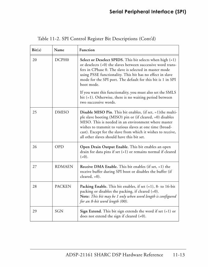
Serial Peripheral Interface (SPI)
20 DCPH0 Select or Deselect SPIDS. This bit selects when high (=1) or deselects (=0) the slaves between successive word trans-fers in CPhase 0. The slave is selected in master mode using PSSE functionality. This bit has no effect in slave mode for the SPI port. The default for this bit is 1 in SPI boot mode.
If you want this functionality, you must also set the SMLS bit (=1). Otherwise, there is no waiting period between two successive words.
25 DMISO Disable MISO Pin. This bit enables, (if set, =1)the multi-ple slave booting (MISO) pin or (if cleared, =0) disables MISO. This is needed in an environment where master wishes to transmit to various slaves at one time (broad-cast). Except for the slave from which it wishes to receive, all other slaves should have this bit set.
26 OPD Open Drain Output Enable. This bit enables an open drain for data pins if set (=1) or remains normal if cleared (=0).
27 RDMAEN Receive DMA Enable. This bit enables (if set, =1) the receive buffer during SPI boot or disables the buffer (if cleared, =0).
28 PACKEN Packing Enable. This bit enables, if set (=1), 8- to 16-bit packing or disables the packing, if cleared (=0). Note: This bit may be 1 only when word length is configured for an 8-bit word length (00).
29 SGN Sign Extend. This bit sign extends the word if set (=1) or does not extend the sign if cleared (=0).
Table 11-2. SPI Control Register Bit Descriptions (Cont’d)
Bit(s) Name Function
ADSP-21161 SHARC DSP Hardware Reference 11-13

SPI IOP Registers
Default value of SPICTL at reset: 0x00008700 Value of SPICTL at slave boot: 0x0A001F81
Baud Rate Example
The BAUDR bit of the SPICTL register sets the baud rate using the following formula:
f SPICLK =
If the core clock is 100MHz and the BAUDR bit is 0xD (13), the SPICLK fre-quency is determined as follows:
f SPICLK = = 3052 Hz
30 SENDZ Send Zero. This bit sends zeros when cleared (=0) or will send the last byte when SPITX empty and bit is set (=1).
31 GM Get Data. This bit fetches incoming data when set (=1) or discards incoming data when cleared (=0). The data that comes in overwrites the previous data in the SPIRX.
Table 11-2. SPI Control Register Bit Descriptions (Cont’d)
Bit(s) Name Function
coreclock
22 BAUDR+------------------------------------
100MHz
22 13+---------------------
11-14 ADSP-21161 SHARC DSP Hardware Reference

Serial Peripheral Interface (SPI)
1=
SPI Status Register (SPISTAT) The SPISTAT register is a read-only register that detects when an SPI trans-fer is complete, if transmission/reception errors occur, and the status of the SPITX and SPIRX FIFOs. Table 11-3 describes the six status bits of the SPISTAT register. See Figure A-44 on page A-138 for the SPISTAT register diagram.
SPIFSPI Tran sm it o r Receive Transfer Com plete1=transfer c om plete, 0=active transfer
MM EMultim aster Error
TXSSPITX D ata Buffer Sta tus (read on ly)
00=SPITX em pty01=TXB p artially full
11=SPITX fu ll10=Reserved
RBSYReception Error (Overflow)
new data received w ith fu ll RXB FIFOSPI enters id le m ode if m aster device
RXS
0=no error, 1=SPIDS~ asserted by slave
TXETransm ission Error (Underflow)1=no new data in TX FIFO, SP I enters id le m ode if m aster device
SPISTAT0xB5
SPIRX Data Buffer Sta tus (read on ly) 00=SPIRX em pty
01=SPIRX pa rtia lly fu ll11=SPIRX fu ll10=Reserved
31 30 29 28 27 26 25 24 23 22 21 20 19 18 17 16
0 0 0 0 0 0 0 0 0 0 0 0 0 0 0 0
15 14 13 12 11 10 9 8 7 6 5 4 3 2 1 0
0 0 0 0 0 0 0 0 0 0 0 0 0 0 0 0
Figure 11-6. SPISTAT Register
ADSP-21161 SHARC DSP Hardware Reference 11-15

SPI IOP Registers
Table 11-3. SPI Status Register Bit Descriptions
Bit(s) Name Definition
0 SPIF SPI Transmit or Receive Transfer Complete. This bit is set (=1) when the SPI transfer is complete and one of the following conditions is met: SPRINT = 1 and the receive buffer is full —or— RDMAEN = 1 and the receive buffer is full—or—SPTINT = 1 and the transmit buffer is empty —or—TDMAEN = 1 and the transmit buffer is empty
1 MME Multimaster Error. This bit is set when a device that is not currently the master device tries to become the master by driving a SPIDS signal while the current master device is communicating to SPI slave devices.
2 TXE Transmission Error. This bit is set when SPI is Slave/Mas-ter, SPTINT = 1 or TDMAEN = 1, but there is no data in SPITX FIFO. If you are not servicing the interrupt quickly enough and not updating the contents of SPITX, this bit is set. In master mode, this means an end of opera-tion and SPI goes into idle mode.
4-3 TXS Transmit Data Buffer Status. These bits indicate the sta-tus of the SPITX data buffer status (read only) as follows: 00 = empty, 01 = partially full, 11 = full.
5 RBSY Reception Error. This bit is set when a data is received with receive buffer full. Either RDMAEN = 1 or SPRINT = 1 and the receive buffer is full. In master mode, this means an end of operation and SPI goes into idle mode.
11-16 ADSP-21161 SHARC DSP Hardware Reference

Serial Peripheral Interface (SPI)
SPI Transmit Data Buffer Register (SPITX)The SPITX transmit data register is a 32-bit register which is part of the IOP register set. The buffer is 3-deep including the shift register. The SPITX register can be accessed by the core or the DMA controller. Data is loaded into SPITX before being transmitted. Prior to the beginning of a data transfer, data in SPITX is automatically loaded into the transmit shift register.
! Do not perform a normal core write during DMA operation. A nor-mal core read of SPITX can be done at any time and does not inter-fere with, or initiate, SPI transfers. A core hang results from writing to a full SPITX buffer.
SPI Receive Data Buffer Register (SPIRX)The SPIRX receive register is a 32-bit read-only register accessible by the core or DMA controller. The buffer is 3-deep including the shift register. At the end of a data transfer, SPIRX is loaded with the shift register data. During a DMA receive operation, the data in SPIRX is automatically loaded into the DMA FIFO. For core or interrupt driven transfer, use the RXS status bits in the SPISTAT register to determine if the receive buffer is full. Reading from an empty SPIRX buffer causes a core hang.
7-6 RXS Receive Data Buffer Status. These bits indicate the status of the SPIRX data buffer status (read only) as follows: 00 = empty, 01 = partially full, 11 = full.
31-8 Reserved
Table 11-3. SPI Status Register Bit Descriptions (Cont’d)
Bit(s) Name Definition
ADSP-21161 SHARC DSP Hardware Reference 11-17

SPI Data Word Formats
SPI Shift RegisterThis register is not directly accessible by the core or DMA controller. The SPI shift register performs both receive and transmit functions. It is clocked on the active edge (cycle boundary for CPHASE=0, sampling edge for CPHASE=1) of the SPICLK clock. It can be shifted right or left depending on the direction of the data flow (LSB first or MSB first) as defined by the DF bit in the SPICTL register. The shift register can also be loaded from the SPITX register with data to be transmitted. The shift register includes 32 shift cells that can be configured to transfer 8-, 16-, and 32-bit words.
SPI Data Word FormatsThe ADSP-21161 SPI supports two transfer formats with respect to clock phases and clock polarities: CPHASE =0 and CPHASE =1. The user applica-tion code can select one of the four combinations of serial clock phase and polarity using the CP and CPHASE bits in the SPICTL register. This section describes the transfer format and word packing for SPI transfers. See Table 11-2 on page 11-11 for SPICTL register bit description.
A master SPI transfer starts when the CPHASE bit is cleared (=0) and the MS bit is set (=1) in the SPICTL register. The SPICLK signal remains inactive for the first half of first cycle of SPICLK. A slave SPI transfer starts as soon as the SPIDS from the master goes low.
When CPHASE is set (=1), the transfer starts with the first edge of SPICLK going from its inactive state to the active state for both slave and the mas-ter devices. A transfer for a slave device is ended with SPIDS negated (inactive on rising edge). For a master device, transfer is considered com-plete after it transmits the last data word or receives the last data word.
The figure “SPI Transfer Protocol” on page 11-20 demonstrates the two basic transfer formats as defined by the CPHASE bit. Two waveforms are shown for SPICLK: one for CP=0 and the other for CP=1. The diagram may be interpreted as a master or slave timing diagrams since the SPICLK, MISO,
11-18 ADSP-21161 SHARC DSP Hardware Reference

Serial Peripheral Interface (SPI)
and MOSI pins are directly connected between the master and the slave. The MISO signal is the output from the slave (slave transmission), and the MOSI signal is the output from the master (master transmission). The SPI-CLK signal is generated by the master, and the SPIDS signal is the slave device select input to the slave from the master. The diagram represents an 8-bit transfer (WL=00) with MSB first (DF=1). Any combination of the WL and DF bits of the SPICTL register is allowed. For example, a 32-bit transfer with LSB first is also a possible configuration.
The clock polarity and the clock phase must be identical for the master device and the slave device involved in the communication link. The transfer format from the master may be changed between transfers to adjust to various requirements of a slave device.
When CPHASE is cleared (=0), the slave select line, SPIDS, must be inactive (HIGH) between each serial transfer. This is controlled automatically by hardware logic. When CPHASE is set (=1), SPIDS may remain active (LOW) between successive transfers or be inactive (HIGH). This can be con-trolled in the SPICTL register with the DCPH0 bit (bit 20).
ADSP-21161 SHARC DSP Hardware Reference 11-19

SPI Data Word Formats
SPI Word Packing
The SPI packs two 8-bit words in a 32-bit word as shown in Figure 10-13. This packing is set by the PACKEN bit in the SPICTL register. These words may be sign extended depending on the SGN bit in SPICTL.
31 0
S S S S S S S S 1
1 if SGN=1, S is the sign bit.if SGN=0, S is 0.
Figure 10-13. SPI Word Packing
Second 8-bit word S S S S S S S S1 First 8-bit word
CP=0, CPH ASE=1
CP=1, CPH ASE=0
SPIDS orFLG [3:0]
SPICLK
SPICLK
SPICLK
SPICLK
CP=0, CPH ASE=0
CP=1, CPH ASE=1
M OSI From M aster MSB LSB
Data Sample Edge
M ISO From Slave
MSB LSB
1 2 3 4 5 6 7 8Cycle n
Figure 11-7. SPI Transfer Protocol
11-20 ADSP-21161 SHARC DSP Hardware Reference

Serial Peripheral Interface (SPI)
SPI Operation ModesThe SPI in ADSP-21161 can be used in a single master or multi-master mode. The MOSI, MISO, and the SPICLK signals are used together in both modes. SPI transmission and reception are enabled simultaneously except for the broadcast mode in which the master writes to multiple SPI devices. The master can receive from only one device at a time. Therefore, each device other than the device to which the master is communicating should have its DMISO bit set (=1). If the transmission or receive is not needed, it can simply be ignored. The following sections describe the SPI operation as a master and as a slave, and in a multi-slave environment. Figure 11-2 shows the master-slave interconnections.
Master Mode OperationWhen SPI is in master mode the interface operates in the following manner:
1. Configure the SPICTL register enabling the device as a master, spec-ifying the appropriate word length, baud rate and any other options needed.
2. Write a data word to the SPITX register using the core.
3. The core sends SPIDS signal to desired slaves using one or more of the FLAG0-3 pins. For more information, see “FLS Functionality in SPICTL for Multiple-Slave Systems” on page 11-23.
4. SPI generates the programmed clock pulses SPICLK and simulta-neously shifts data out of MOSI and in from MISO. Before starting the shift, the shift register is loaded with the contents of the trans-mit data buffer register SPITX. At the end of the transfer, the receive data buffer register SPIRX is loaded with the contents of the shift register.
ADSP-21161 SHARC DSP Hardware Reference 11-21

SPI Operation Modes
5. SPI sends or receive words. Depending on the function it is per-forming and assuming all interrupts (receive/transmit) are enabled, SPI generates interrupts. An SPI interrupt occurs when SPITX is partially empty and the receive buffer SPIRX is partially full.
6. To specify receive data only, set the RDMAEN/SPRINT bits in the SPICTL register. If the receive DMA is enabled, it is not necessary to enable the interrupt. In this case, the transmitted data can be all 0s after the initial words have been transmitted. For more informa-tion, see the SENDZ bit in the SPICTL register.
7. To transmit data, set the TDMAEN/SPTINT bits in the SPICTL register. If the transmit DMA is enabled, it is not necessary to enable the interrupt. In this case, the received data overwrites the previous words in the receive buffer. For more information, see the GM bit in the SPICTL register.
Interrupts are automatically generated when the transmit buffer is par-tially empty or when the receive buffer is partially full. In the event that the SPITX and SPIRX interrupts are not serviced, causing the transmit buffer to empty or the receive buffer to fill, the SPI device continues to operate based on the conditions of the SENDZ bit and GM bit.
If SENDZ is cleared (=0) and the transmit buffer is empty, the device repeat-edly transmits 0s on the MOSI pin. If SENDZ is set (=1) and the transmit buffer is empty, the device repeatedly transmits the last word that was in SPITX before the transmit buffer became empty.
If GM is set (=1) and the receive buffer is full, the device continues to receive new data from MISO pin, overwriting the older data in the SPIRX buffer. If GM is cleared (=0) and the receive buffer is full, the incoming data is discarded, and the SPIRX register is not updated.
11-22 ADSP-21161 SHARC DSP Hardware Reference

Serial Peripheral Interface (SPI)
FLS Functionality in SPICTL for Multiple-Slave Systems
The FLS bits in the SPICTL register are used in a multiple-slave SPI envi-ronment. For example, if there are five SPI devices in the system with a ADSP-21161 master, the master ADSP-21161 supports the SPI mode transactions across all four other devices. This configuration requires that only one ADSP-21161 is master within this multi-slave environment. The four flag pins (FLAG0, FLAG1, FLAG2, and FLAG3) on the ADSP-21161 mas-ter can be connected to each of the slave SPI device's SPIDS pin. In this configuration, the FLS bits are used in the following ways.
• The ADSP-21161 transmits to all the four SPI devices at the same time in a broadcast mode.
• The ADSP-21161 receives and transmits from one SPI device by enabling only one slave SPI device at a time
Automatic Slave Selection
Multiple slaves are automatically selected by enabling the PSSE bit in the SPICTL register. To enable different slaves, connect the slave SPIDS pins are connected to the programmable flag pins (FLAG0,FLAG1,FLAG2 and FLAG3) of the master ADSP-21161. By writing to the SPICTL bits 15-18, corre-sponding FLAG bits are programmed as outputs for slave selection. This asserts the FLAG0,FLAG1,FLAG2 and FLAG3 pins low by asserting the SPIDS of the slaves. Upon completion of the transfer, the FLAG pins are de-asserted, thereby disabling the slave selection.
ADSP-21161 SHARC DSP Hardware Reference 11-23

SPI Operation Modes
Slave Mode OperationTo prepare for the data transfer, a slave DSP writes the data to be trans-mitted into the transmit FIFO. The following steps illustrate SPI operation in slave mode.
1. Configure the SPICTL register.
2. Once the core receives the SPIDS signal from the master, its starts sending or receiving data on the proper SPICLK edge.
3. Reception/transmission continues until SPIDS is negated.
Interrupts are automatically generated when the transmit buffer is par-tially empty or when the receive buffer is partially full. In the event that the transmit and receive interrupts are not being serviced and subse-quently causing the transmit buffer to empty or the receive buffer to fill, the SPI device continues to operate based on the conditions of the SENDZ and GM bits.
If the SENDZ bit is cleared (=0) and the transmit buffer is empty, the device repeatedly transmits 0s out on the MISO pin. If the SENDZ is set (=1) and the transmit buffer is empty, the device continues to transmit the last word written to SPITX that was transmitted. Retransmission of the data in SPITX occurs after the transmit buffer becomes empty.
If the GM bit is set (=1) and the receive buffer is full, the device continues to receive new data from the MOSI pin, overwriting the previous (older) data in the SPIRX buffer. If the GM bit is reset (=0) and the receive buffer is full, the incoming data from the shift register is discarded and the SPIRX register is not updated. The register ignores the new data and retains the old information.
11-24 ADSP-21161 SHARC DSP Hardware Reference

Serial Peripheral Interface (SPI)
Error Signals and FlagsPlease refer to the SPISTAT register definition in Table 11-3 on page 11-16 for the following discussion.
Multi-Master Error (MME)The MME bit is set (=1) in the SPISTAT register when the SPIDS pin of a mas-ter ADSP-21161 is driven low by another device in the system. This occurs when another device is trying to be the master. This can cause con-tention between two drivers and push-pull CMOS drivers. When this error is detected, the following actions take place:
1. The MS control bit in SPICTL is cleared (= 0), configuring the SPI interface as a slave.
2. The SPIEN bit in SPICTL is also cleared, disabling the SPI system.
3. The MME status bit in SPISTAT is set. This bit can be polled to test whether this error condition has occurred.
Transmission Error (TXE)This error bit is set in the SPISTAT register when SPI is enabled and there is no data in the transmit FIFO (SPITX is empty). This signals the end of the transmission. In master mode, if the SPTINT or TDMAEN are set and there is no data in the transmit buffer, the device goes into idle mode. The TXE bit is set. At this point, the device is no longer the master.
Also, when the device is selected by another master device and the trans-mit buffer is empty, this error bit is set. Data that is transmitted is specified by the SENDZ bit’s condition in the SPICTL.
TXE is cleared (=0) in the following cases: when SPITX is empty, when SPIRX is full, or when SPIEN is disabled.
ADSP-21161 SHARC DSP Hardware Reference 11-25

SPI/Link Port DMA
Reception Error (RBSY)This flag is set in the SPISTAT register when the device is still receiving data but there is no space in the receive FIFO. In other words, the new receive transfer is complete before the previous data is properly loaded into the SPIRX register. This may occur in the following ways:
1. The receive DMA is enabled but is not getting a grant — the receive buffer is becoming full.
2. The receive interrupt is enabled but is not being serviced — the receive buffer is full.
Whether new data overwrites the older data or is discarded depends on the GM bit in the SPICTL. If the GM bit is set (=1) and the SPIRX register is still full, this error occurs. If GM is cleared (=0), starting new transfer with both the shift register and the SPIRX registers full causes this error. Therefore, depending on the GM bit setting, the SPIRX register may be updated with the newly received data.
This bit is cleared (=0) in the following cases: when SPITX is empty, when SPIRX is full, or when SPIEN is disabled.
SPI/Link Port DMA The SPI shares DMA channels 8 and 9 with the link port. The receive DMA is shared with link port 0 DMA, and the transmit DMA is shared with link port 1 DMA.
" Do not enable SPI and link port DMA simultaneously. SPI and link port are mutually exclusive when one of the peripherals is enabled.
SPI DMAs have higher priority than link port DMAs. If SPI DMAs must be enabled, disable link port DMAs and pending link port DMA requests. For more information, see “SPI Port DMA” on page 6-101.
11-26 ADSP-21161 SHARC DSP Hardware Reference

Serial Peripheral Interface (SPI)
Master Mode DMA OperationFor transmit DMA operations, if the DMA controller is unable to keep up with the transmit stream, due perhaps to heavy DMA channel activity, the transmit port operates according to the state of the SENDZ bit. If SENDZ is cleared (=0) and the DMA buffer is empty, the device repeatedly transmits 0s on the MOSI pin. If SENDZ is set (=1) and the DMA buffer is empty, the DMA controller repeatedly transmits the last word transmitted before the DMA buffer became empty. After the first word is transferred, the receive buffer is assumed to be full in this mode.
For receive DMA operations, if the DMA controller is unable to keep up with the receive data stream, the receive buffer operates according to the state of the GM bit. If GM is set (=1) and the DMA buffer is full, the device continues to receive new data from the MISO pin, overwriting the older data in the SPIRX buffer. If GM is cleared (=0) and the receive buffer is full, the incoming data is discarded, and the SPIRX register is not updated. While performing a receive DMA, the transmit buffer is assumed to be empty.
Do not write to the SPITX register during an active SPI transmit DMA operation because DMA data will be overwritten. Writes to the SPITX reg-ister during an active SPI receive DMA operation are allowed. Reads from the SPIRX register are allowed at any time. Interrupts are generated based on DMA events that are configured in the SPICTL register and in the CPx register for DMA chaining.
A master SPI DMA sequence may involve back-to-back transmission and/or reception of multiple chained DMA transfers. The SPI controller supports such a sequence with no DSP core interaction.
ADSP-21161 SHARC DSP Hardware Reference 11-27

SPI Booting
Slave Mode DMA OperationWhen the DMA controller transmits or receives data in slave mode, the start of a transfer is triggered by a transition of the SPIDS signal to the active-low state or by the first active edge of SPICLK.
For transmit DMA operations, if the DMA engine is unable to keep up with the transmit stream, the transmit port operates according to the state of the SENDZ bit. If SENDZ is cleared (=0) and the DMA buffer is empty, the device repeatedly transmits 0s on the MISO pin. If SENDZ is set (=1) and the DMA buffer is empty, it repeatedly transmits the last word transmitted before the DMA buffer became empty. After the first word is transferred, the receive buffer is assumed to be full in this mode.
For receive DMA operations, if the DMA controller is unable to keep up with the receive data stream, the receive buffer operates according to the state of the GM bit. If GM is set (=1) and the receive buffer is full, the device continues to receive new data from the MOSI pin, overwriting the older data in the SPIRX buffer. If GM is cleared (=0) and the receive buffer is full, the incoming data is discarded.
Do not write to the SPITX register during an active SPI transmit DMA operation. Writes to the SPITX register during an active SPI receive DMA operation are allowed. Reads from the SPIRX register are allowed at any time. Interrupts are generated by unmasking the SPI channel bit in the IMASK register for single-shot, non-chained DMA transfers.
SPI BootingThe ADSP-21161 allows a host SPI device to boot the ADSP-21161 on power-up RESET de-assertion. To enable the SPI booting mode, the EBOOT and BMS pins must be tied low, and the LBOOT pin must be tied high. When the DSP is in the SPI boot configuration and resets, the DSP starts the SPI boot process. The ADSP-21161 is configured as a slave upon power-up. Therefore, after reset the ADSP-21161 goes into an idle state identical to
11-28 ADSP-21161 SHARC DSP Hardware Reference

Serial Peripheral Interface (SPI)
that caused by the IDLE instruction. The DSP waits for the SPI host to download the boot program.
The default address of the SPICTL register when the DSP is configured for SPI boot is 0x0A00 1F81. The SPI port is enabled as a slave to receive 32-bit words in LSB-first format. DMA is enabled to facilitate loading the boot kernel. The DMISO bit is also enabled to accommodate systems where multiple slave devices are to be booted simultaneously.
DMA channel 8 is used when downloading the boot kernel information to the DSP. At reset, the DMA parameter registers for DMA channel 8 are initialized to their required values. Table 11-4 lists the initial values for these registers.
The ADSP-21161 SPI booting mode supports boots from 8-, 16-, or 32-bit host SPI devices. In SPI boot mode, the data word size in the shift register defaults to 32 bits. Therefore, for 8- or 16-bit hosts, data words are packed into the shift register to generate 32-bit words, which can be shifted into internal program memory.
! In SPI-boot mode, the data word size in the shift register defaults to 32-bits.
The host initiates the booting operation by activating SPICLK and asserting the SPIDS signal to the active low state. The 256-word, boot-strapped
Table 11-4. Parameter Initialization Value
Parameter Register Initialization Value
IISRX 0x0004 0000
IMSRX 0x0000 0001
CSRX 0x0000 0180
GPSRX uninitialized
ADSP-21161 SHARC DSP Hardware Reference 11-29

SPI Booting
instruction loader kernel is loaded 32 bits at a time, via the 32-bit SPI shift register. To properly upload 256 instructions (48-bit words), the SPI DMA initially loads a DMA count of 0x180 (384) 32-bit words which is equivalent to 0x100 (256) 48-bit words. The relationship between the 32-bit words received into the SPIRX register and the instructions that need to be placed in internal memory are described in the Figure 11-8.
After the first 256 words are loaded the interrupt associated with the SPI receive is activated. The processor jumps to the location for SPIRI_svc (0x40040) and executes the code located there. Typically, the first instruc-tion at the SPI receive interrupt vector (SPIRI) is an RTI instruction in which case the processor jumps to location 0x40005 where normal pro-gram execution continues. Because most applications require more than 256 words of instructions and initialization data, a loader and a 256 word loader kernel are supplied with the tools. Use these tools to create code that automatically loads the rest of the application code and then over-write itself with application code and data. For more information on the loader, see the development tools documentation.
The boot loader kernel supplied with the tools loads a combination of instructions with DMA into scratch locations and then writing the instructions to internal memory using the core via the PX register. The 256-word, boot-strapped instruction loader kernel is loaded 32-bits at a time, via the 32-bit SPI shift register, using a normal-word addressing scheme with two-column memory addresses. Figure 10-13 shows how SPI data is packed in internal memory.
11-30 ADSP-21161 SHARC DSP Hardware Reference
Serial Peripheral Interface (SPI)
-bit s
The SPI Control Register (SPICTL) is configured to 0x0A00 1F81 upon reset during SPI boot. SPI transfers occur with the following default bit settings:
• SPIEN = 1, SPI enabled
• MS = 0, slave device
• DF = 0, MSB first
• WL = 11, 32-bit SPI receive shift register word length
• BAUDR = 1111, baud rate is set but not used since the device is a slave
• DMISO = 1, MISO disabled
• RDMA = 1, SPIRX DMA enabled on channel 8
32-Bit receive SHIFT
REGISTER
S
DM A #1: DM [40000]M SW LSW
1 2 3 4
PM 48 [0x400FF]
16
DM A #2: DM [40001]M SW LSW
DM A #3: DM [40002]M SW LSW
PM 48 [0x40003]
DM A #6: DM [40005]M SW LSW
M OSI
256 48w ord
0x400FF
0x40000
DM A #4: DM [40003]M SW LSW
PM 48 [0x40002]
DM A (channel 8)
PIRX PM 48 [0x40001]
DM A #5: DM [40004]M SW LSW
PM 48 [0x40000]
#384:DM [0x4017F]M SW LSW
#384:DM [0x4017E]M SW LSW
[x40001]
[x400FE]
[x40002]
LWU W
Figure 11-8. SPI Data Packing
ADSP-21161 SHARC DSP Hardware Reference 11-31

SPI Booting
6D
ory
This configuration sets up the SPIRX register for 32-bit serial transfers. The SPIRX DMA channel 8 parameter registers are configured to DMA in 0x180 32-bit words into internal memory normal-word address space starting at 0x40000. Once the 32-bit DMA completes, the data is then accessed as 3-column 48-bit instruction accesses, i.e., the DSP executes a 256 (0x100) word loader kernel upon completion of the 32-bit, 0x180 word DMA.
! For 16-bit SPI hosts, two words must be shifted into the 32-bit receive shift register before a DMA transfer to internal memory occurs. For 8-bit SPI hosts, four words must be shifted into the 32-bit receive shift register before a DMA transfer to internal mem-ory occurs.
By default, the booting SPI expects to receive words into SPIRX seemlessly. This means that bits are received continuously without breaks. For differ-ent SPI host sizes, the DSP expects to receive instructions and data packed in an LSW format.
The following figure shows how a pair of instructions are packed for SPI booting using a 32-, 16- , and an 8-bit host.
16-bit host
CCDD1122
1122
33445566 7788AABB
CCDD AABB 778833445566
66 55 44 33 22 11 DD CC BB AA 88 77
32-bit host
8-bit host
[0x40000] 1122 3344556[0x40001] 7788 AABBCCD
Words Instructions In Internal Mem
Figure 11-9. Instruction Packing for 32-, 16-, or 8-bit SPI Host Booting
11-32 ADSP-21161 SHARC DSP Hardware Reference

Serial Peripheral Interface (SPI)
The following sections examine how data is packed into internal memory during SPI booting for SPI host word widths of 32-, 16-, or 8-bits.
32-bit SPI Host BootFigure 11-10 shows 32-bit SPI host packing of 48-bit instructions. The 32-bit word is shifted to internal program memory during loading of the 256-word kernel.
The following is an example of 48-bit instructions to be executed at PM addresses 0x40000 and 0x40001:
[0x40000] 1122 33445566[0x40001] 7788 AABBCCDD
The 32-bit SPI host would need to pack (prearrange data) as follows:
SPI word 1 = 0x33445566SPI word 2 = 0xCCDD1122SPI word 3 = 0x7788AABB
S
DMA
PIRX
Internal Mem ory
0x40000
0x400FF32- b
it S
PI W
OR
D N
MO SI
32 32 32
Channel 8 (LoaderKernel)
Figure 11-10. 32-bit SPI Host Packing
ADSP-21161 SHARC DSP Hardware Reference 11-33

SPI Booting
16-bit SPI Host BootFigure 11-11 shows 16-bit SPI host packing of 48-bit instructions. For 16-bit hosts, two 16-bit words are packed into the shift register to gener-ate a 32-bit word. The 32-bit word is shifted to internal program memory during loading of the kernel.
The following is an example of 48-bit instructions to be executed at PM addresses 0x40000 and 0x40001:
[0x40000] 1122 33445566[0x40001] 7788 AABBCCDD
The 16-bit SPI host would need to pack (prearrange data) as follows:
SPI word 1 = 0x5566SPI word 2 = 0x3344SPI word 3 = 0x1122SPI word 4 = 0xCCDDSPI word 5 = 0xAABBSPI word 6 = 0x7788
SPIRX
DM A Internal M em ory
0x40000
0x400FF
16-b
it W
OR
D N
MO SI
16-b
it
WO
RD
N +
1
32 3232
(LoaderKernel)
Channel 8
Figure 11-11. 16-bit SPI Host Packing
11-34 ADSP-21161 SHARC DSP Hardware Reference

Serial Peripheral Interface (SPI)
The initial boot of the 256-word loader kernel requires a 16-bit host to transmit 768 16-bit words. One 32-bit word is created from two packed 16-bit words. The SPI DMA count value of 0x180 is equivalent to 384 words. Therefore, the total number of 16-bit words loaded is 768.
8-bit SPI Host BootFigure 11-12 shows 8-bit SPI host packing. For 8-bit hosts, four 8-bit words are packed into the shift register to generate a 32-bit word. The 32-bit word is then shifted to internal program memory during loading of the 256-instruction word kernel.
S
DMA
PIRX
Internal Mem ory
MOSI
8-bi
t
WO
RD
N
+ 3
8-bi
t
WO
RD
N
+ 2
8-bi
t
WO
RD
N
+ 1
8-bi
t
WO
RD
N
0x40000
0x400FF
32 3232
(LoaderKernel)
Channel 8
Figure 11-12. 8-bit SPI Host Packing
ADSP-21161 SHARC DSP Hardware Reference 11-35

SPI Booting
The following is an example of 48-bit instructions to be executed at PM addresses 0x40000 and 0x40001:
[0x40000] 1122 33445566[0x40001] 7788 AABBCCDD
The 8-bit SPI host would need to pack (prearrange data) as follows:
SPI word 1 = 0x66SPI word 2 = 0x55SPI word 3 = 0x44SPI word 4 = 0x33SPI word 5 = 0x22SPI word 6 = 0x11SPI word 7= 0xDDSPI word 8 = 0xCCSPI word 9 = 0xBBSPI word 10 = 0xAASPI word 11 = 0x88SPI word 12 = 0x77
The initial boot of the 256-word loader kernel requires an 8-bit host to transmit 1536 8-bit words. The SPI DMA count value of 0x180 is equal to 384 words. Since one 32-bit word is created from four packed 8-bit words, the total number of 8-bit words transmitted is 1536.
Multiprocessor SPI Port Booting
In systems where multiple ADSP-21161s are connected and configured for SPI booting, the master ADSP-21161 (or any SPI master device) can boot up to four ADSP-21161s configured as SPI slaves. The DSP uses four programmable flags, FLAG0-3, as dedicated SPI device-select signals for the SPI slave devices. The FLS bits in the SPICTL register correspond to these flags.
11-36 ADSP-21161 SHARC DSP Hardware Reference

Serial Peripheral Interface (SPI)
Figure 11-13 shows a single ADSP-21161 master with four slaves. The master processor selects each slave device using a dedicated FLAG pin. The master device communicates with one slave device at any given time, or it broadcasts data to multiple slaves by setting more than one FLS bit in SPICTL.
The master ADSP-21161 can boot multiple slaves in the following ways:
• The ADSP-21161 transmits to all four SPI devices at the same time in a broadcast mode. Broadcast the 256-word loader kernel and identical application code simultaneously to all slaves. If the master is a ADSP-21161, enable the FLSx bit in the SPICTL register, and dis-able the MISO pins. Otherwise, the master asserts the SPID pins of all the slaves to transmit the data.
This feature can be enabled by setting the DMISO bit in the four slave processors. This DMISO feature may be available in some microcon-trollers. Therefore, it is possible to use the DMISO feature with any SPI devices that include this functionality.
• Load the bootstrap kernel and DSP instructions and data one-at-a time for each processor. In this case, enable only one FLSx bit at a time in the SPICTL register to drive the flag pin connected to a slave's device select. The master device will assert the SPIDS pin of the slave to load the data. This ensures that each processor boots one after the other.
• It is also possible to use a combination of broadcast and individual processor booting to boot a multiprocessor system. SPI hosts can broadcast boot application code that will reside on several slaves and then complete the booting process by booting the individual slaves with slave specific application code. In this situation, the host SPI device asserts the SPIDS pins of all slaves during the broadcast por-tion of the boot. The host then asserts the SPIDS pins of specific
ADSP-21161 SHARC DSP Hardware Reference 11-37
SPI Booting
slaves. If the ADSP-21161 is the master as is shown in Figure 11-13, the master enables the FLSx bit in the SPICTL register for the slave currently booting.
Figure 11-13 shows one ADSP-21161 as a master and four ADSP-21161 (or other SPI-compatible devices) as slaves:
Figure 11-13. Single Master, Multiple Slaves Configuration — All ADSP-21161s
MISO MO SISPIC LK SPIDS
SlaveDevice
MISO MO SISPIC LK SPIDS MISO MO SISPIC LK
MISO MO SISPIC LK SPIDS
SlaveDevice
SlaveDevice
ASP-21161NSingle M aster
Dev ice
FLAG1
FLAG2
FLAG3
VDD
FLAG0
SPIDSMISO MO SISPIC LK SPIDS
SlaveDevice
11-38 ADSP-21161 SHARC DSP Hardware Reference

Serial Peripheral Interface (SPI)
SPI Programming ExampleThis section provides one programming example written for the ADSP-21161 DSP. The core-driven interrupt SPI loopback example in Listing 11-1 demonstrates how the core reads from the SPI receive buffer and writes to the SPI transmit buffer. For a DMA programming example, see Listing 6-7 on page 6-109.
Listing 11-1. Core-Driven Interrupt SPI Loopback
/*_______________________________________________________________ADSP-21161 Core-Driven Interrupt SPI Loopback Example
This example shows looped-back SPI 32-bit transfer. On this peripheralloop-back is performed by externally connecting the hardware MOSI and MISO pins on the DSP. After receiving an interrupt, the core directly writes to the transfer buffer (SPITX) and reads from the receive buffer (SPIRX). _______________________________________________________________*/#include <def21161.h>#define size 10
// Reserved vector location.section/pm seg_rsvd1;Reserved_1: rti; nop; nop; nop;
// Vector code for reset vector from ldf file.section/pm seg_rth;Chip_Reset: idle; jump start; nop; nop;
// Vector code for receive interrupt vector from ldf file.section/pm spiri_svc;nop; nop; jump receive; rti;
.section/ dmseg_dmda;
.var spi_tx_buf[size] =0x11111111,0x22222222, 0x33333333, 0x44444444, 0x55555555, 0x66666666, 0x77777777, 0x88888888, 0x99999999, 0xaaaaaaaa;.var spi_rx_buf[size];
.section/pm seg_pmco;
start:
ADSP-21161 SHARC DSP Hardware Reference 11-39

SPI Programming Example
//Set pointers for source and dest, I0=B0 automaticallyb0=spi_tx_buf; // 32-bit SPI datawordsl0=@spi_tx_buf;m0=1;b1=spi_rx_buf; // 32-bit SPI datawordsl1=@spi_rx_buf;m1=1;
ustat1 = dm(SYSCON);bit clr ustat1 BHD;// Clear BHD in SYSCON to disable core buffer hangdm(SYSCON) = ustat1;
bit set mode1 CBUFEN; // Set circular buffer enable
bit set LIRPTL SPIRMSK ; // Enable SPI RX interruptsbit set MODE1 IRPTEN; // Allow global interruptsbit set IMASK LPISUMI; // Unmask spi interrupts
r0=0x00000000; // Initially clear SPI control registerdm(SPICTL)=r0;
// Prime SPITX registerr0=dm(i0,m0);dm(SPITX)=r0;
ustat1=dm(SPICTL); // Set up options for the SPI port bit set ustat1 SPIEN | SPRINT | SPTINT | MS | CPHASE | DF | WL32 | BAUDR5 | SGN | GM;
/* Enable SPI port, SPITX and SPIRX interrupts, master deviceSPICLK toggles at beginning of first data transfer bit. Use MSB first format, 32 bit word length, baud rate sign extend, and get more new data even if receive buffer is full */
dm(SPICTL) = ustat1; // Start transfer by configuring SPICTL
wait: idle; jump wait;
receive: r0=dm(SPIRX); //Read SPIRXdm(i1,m1)=r0; //Write value to internal memory bufferr0=dm(i0,m0);//Get new value to transmit from internal transmit bufferdm(SPITX)=r0; //Write value to SPITXrti;
11-40 ADSP-21161 SHARC DSP Hardware Reference