Embed Size (px)
Citation preview

132
Figure 10.1. Construction nears completion at Harvard University (left) on the new Laboratory for
Integrated Science and Engineering (LISE), November 2006. Computer aided design of the completed LISE
building (right) that will be the new home of the shared experimental facilities.
10. SHARED AND OTHER EXPERIMENTAL FACILITIES
The shared facilities are operated to encourage both hands-on research by experienced
and qualified users, and as educational tools for students and researchers from other
disciplines who can benefit from their use. A broad-range of facilities teaches students
the skills of nanofabrication, imaging, and synthesis that they will need after graduation,
and open new avenues of investigations for all disciplines. The shared experimental
facilities play a special role in fostering interdisciplinary exchanges. The facilities are the
natural meeting places where students from all parts of the Center learn from one
another and share technical expertise.
New Laboratory Construction
Harvard University is supporting the construction of a new, 135,000 sq. ft. Laboratory
for Integrated Science and Engineering (LISE). The Faculty Planning Committee viewed
the construction of LISE, in close proximity to other science buildings in the north Yard,
as a singular opportunity to create a research environment that will centralize major
experimental facilities and foster cross-disciplinary research. The principal architect of
LISE is Jose Rafael Moneo who served as Chairman of the Architecture Department of
the Harvard Graduate School of Design (1985–1990). The building will include
extensive vibration-free space to house the shared facilities including major cleanroom
and nanofabrication facilities, advanced imaging laboratories, and facilities for materials
synthesis. The building will also have space for new faculty (Interdisciplinary Research
Laboratories) to advance cross-disciplinary research. A third programmatic element will
be common spaces to promote collaborative exchanges. The project is now entering the
final construction phase (Fig. 10.1). LISE is scheduled to open in summer of 2007. The
University is planning the acquisition of new instrumentation for LISE as well as the

133
Figure 10.3. Dr. Jiandi Wan uses the new
Asylum MFP-3D AFM instrument in Bauer
Laboratory, as Dr. Richard Schalek, CNS
senior staff, assists.
relocation of current equipment, from five different buildings where the shared facilities
are now located, with the transition occurring through the remainder of the year.
Harvard University supported the construction of a new building in the North Yard at 60
Oxford Street. The top two
floors, along with one floor in
the adjacent Engineering
Sciences Lab (ESL) at 40
Oxford Street are now home to
faculty in Bioengineering.
Assistant Professor Parker’s
laboratories have been finished
in this space which has been an
impetus for collaborative work
in the Tools for Integrated
Nanobiology Cluster, for
example. The University has
also recently completed the
construction of new laboratory
space for undergraduate
bioengineering training (Fig.
10.2). These recent buildings
and teaching laboratories will
continue to pull the science community together, across traditional departmental
boundaries and be spaces where researchers can interact in new common experimental
and training facilities.
Integrated Management of Facilities and Technical Staff
In January 1999 Harvard announced the
commitment to launch several new
interdisciplinary research centers in the
sciences. The faculty had identified a strong
scientific and technological need for the
understanding and development of mesoscale
materials and structures. This new challenge
would require sophisticated facilities for
imaging, nanofabrication, synthesis, and
growth. The Center for Imaging and Mesoscale
Structures (CIMS) was born from this vision.
Halperin, co-PI of NSEC, was the first
Scientific Director of CIMS. Harvard
University supports the Center for Imaging and
Mesoscale Structures (CIMS) to support
research and education in the area of
nanotechnology and mesoscale science. A main mission of CIMS is the provision,
Figure 10.2. New bioengineering undergraduate teaching
laboratories in Pierce Hall.
134
operation and maintenance of complex facilities for imaging and fabrication. CIMS
began to purchase equipment and hire technical staff as well as construct a second
cleanroom in the basement of the Gordon McKay Laboratory. The management of the
shared facilities at Harvard from CIMS, MRSEC and NSEC were integrated in 2002; the
management boards of these Centers work closely together. Importantly, instrumentation
for new CIMS facilities are open to all students, research associates, staff and faculty of
the NSEC (regardless of institution), and to all NSEC collaborators. This integration
made CIMS the main source for centralized user facilities in the Oxford Street science
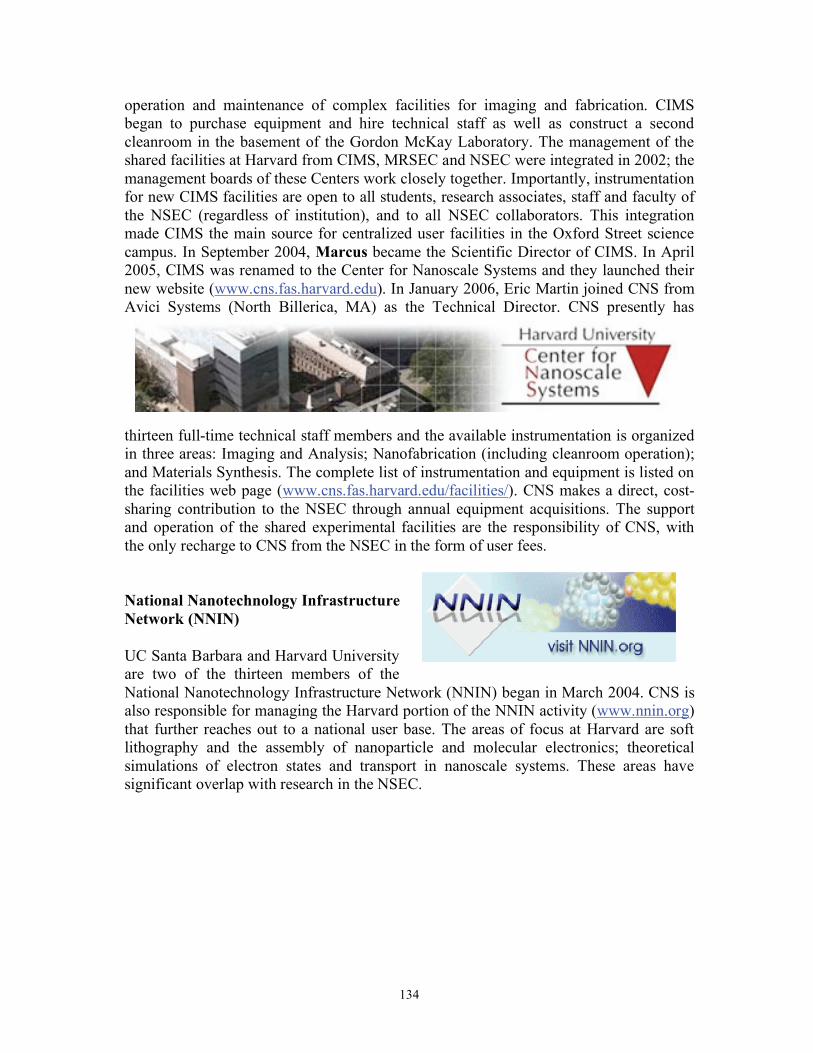
campus. In September 2004, Marcus became the Scientific Director of CIMS. In April
2005, CIMS was renamed to the Center for Nanoscale Systems and they launched their
new website (www.cns.fas.harvard.edu). In January 2006, Eric Martin joined CNS from
Avici Systems (North Billerica, MA) as the Technical Director. CNS presently has
thirteen full-time technical staff members and the available instrumentation is organized
in three areas: Imaging and Analysis; Nanofabrication (including cleanroom operation);
and Materials Synthesis. The complete list of instrumentation and equipment is listed on
the facilities web page (www.cns.fas.harvard.edu/facilities/). CNS makes a direct, cost-
sharing contribution to the NSEC through annual equipment acquisitions. The support
and operation of the shared experimental facilities are the responsibility of CNS, with
the only recharge to CNS from the NSEC in the form of user fees.
National Nanotechnology Infrastructure
Network (NNIN)
UC Santa Barbara and Harvard University
are two of the thirteen members of the
National Nanotechnology Infrastructure Network (NNIN) began in March 2004. CNS is
also responsible for managing the Harvard portion of the NNIN activity (www.nnin.org)
that further reaches out to a national user base. The areas of focus at Harvard are soft
lithography and the assembly of nanoparticle and molecular electronics; theoretical
simulations of electron states and transport in nanoscale systems. These areas have
significant overlap with research in the NSEC.
135
Figure 10.4. Michael Stopa speaking at a NISE-net
Forum at the Museum of Science, Boston.
Michael Stopa leads the coordination
of the computational initiative in
NNIN (Fig. 10.4). Stopa was
previously at NTT in Japan and gave
several seminars as part of the
international exchange programs of the
NSEC. Like the NNIN experimental
program, NNIN/C is a multi-university
initiative, the object of which is to
establish a national computing
resource that provides hardware
resources and simulation tools
dedicated to nanoscience research for
the academic and industrial research
communities. The software tools include commercial software packages for design and
analysis, of nanometer scale devices as well as some of the latest academic advances in
nanoscale modeling and simulation software. A workshop Synergy Between Experiment
and Computation in Nanoscale Science was held from May 31–June 3, 2006 (Fig. 10.5)
that attracted over 100 participants, from other NNIN computational sites, across the
nation, and from 12 countries. NSEC speakers at the workshop included Heller,
Kaxiras, Marcus, and Whitesides.
Figure 10.5. NNIN/C Conference activities, 2006.

136
Figure 10.6. Dr. Fettah Kosar (left); George Whitesides (right) giving keynote presentation at Soft
Lithography Technical Forum on Halloween, 2006.
In August 2006, Fettah Kosar joined the CNS/NNIN team as a senior staff scientist (Fig.
10.6) to oversee the operation of the Soft Lithography Foundry (SLF), support academic
and industrial researchers on projects, and train users on master fabrication and soft
lithography. Fettah completed his Ph.D. in Bioengineering and Nanotechnology from the
University of Washington in 2005. Before joining CNS, Fettah was a senior fellow in
Paul Yager’s group at UW, working on the design and development of a microfluidic
point-of-care system for the rapid and on-the-field diagnosis of life-threatening
infectious diseases in third-world countries.
Inline with the NNIN mission, CNS organized a Soft Lithography Technical Forum,
which was held on Harvard University campus in Cambridge on October 31st and
November 1st, 2006. This event was the second in a series of Technical Forums
organized by individual NNIN sites. The main goal of the Forum was to disseminate and
share technical knowledge and practical information on soft lithography across NNIN
sites, as well as to educate and train NNIN personnel on some basic soft lithography
techniques. Subject matter included overviews from participating sites, expert
presentations, hands-on training sessions, laboratory demos, and tours of functional
facilities.
Fourteen participants from ten NNIN sites attended this forum, excluding the CNS staff
members. After opening remarks by Charles Marcus and Eric Martin, the forum took
off with a stimulating keynote presentation from George Whitesides, who addressed a
full house about his vision of the NNIN Soft Lithography Network. After the keynote, it
was time for the NNIN site presentations, which promoted sharing soft lithography-
related experience and knowledge among the NNIN sites. Overall, the Soft Lithography
Technical Forum was received and rated very favorably by the attendees. Whereas this
forum was an internal NNIN event, CNS is currently considering a much larger Soft
Lithography Workshop at Harvard University for the Fall of 2007. Unlike the NNIN
Soft Lithography Technical Forum, this workshop will be open to anyone interested in
soft lithography, not just the NNIN sites.

137
Figure 10.7. Shared Facilities user statistics from March 2006 to February 2007.
User Statistics
The shared facilities are heavily subscribed with more than 560 users from March 2006
through February 2007. Users came from many different institutions and varied
technical fields. Below (Fig. 10.7) is statistical information of the shared facility users.
Note that the Other category in the Institution Type chart includes small and large
corporations, state and federal agencies, and international institutions. Also, most
projects cut across many technical fields. In fact, it is part of the mission of CNS and
NNIN to promote such interdisciplinary research. However, for the sake of tracking
trends, users must select only one technical field when applying to the CNS/NNIN User
Program.

138
Figure 10.8. (Left) Dr. Steve Cronin and Sasha Stolyarov (REU, Univ. Texas Dallas) working in one of
the cleanrooms; (right) Joseph Cox (REU, Eastern Nazarene College) and Visiting Professor John Free,
during the summer research experience program, 2006.
Student Training and Safety
Equally important to the acquisition of state-of-the-art instrumentation in the pursuit of
our research program, is the availability of talented technical staff that provides training
through regularly scheduled courses and hands-on laboratory instruction. The technical
staff ensures that environmental health and safety procedures are followed and guidance
is provided until researchers are certified as self-users. The staff also helps researchers
develop new fabrication processes and measurements techniques, and upgrade
equipment in response to changing research needs.
These cutting-edge instruments also are used in many of the Research Experience for
Undergraduate (REU) and Teacher (RET) projects and, in many cases, are resources that
are not available to many participants in these summer research programs back at their
home institutions (Fig. 10.8). This is an important illustration how the NSEC brings
together talented researchers, who serve as mentors for undergraduates and teachers,
technical staff with expertise, and essential (and often sophisticated) experimental
facilities. Sasha Stolyarov (above) returned to Harvard after finishing his undergraduate
degree at the Univ. of Texas at Dallas and entered Harvard as a graduate student in the
Department of Physics. Sasha was awarded an NSF Graduate Fellowship this past year.
Other Facilities
Center participants have access to other imaging, clean room, and synthesis facilities at
MIT and UC Santa Barbara. With the installation of three new systems (Fig. 10.9), there
are now a total of eight different MBE machines available for sample growth at UC
Santa Barbara (www.materials.ucsb.edu/~mbe/lablayout.html). The NSEC has supported
exchanges through the travel program by students who are expert in materials growth
(UC Santa Barbara) to meet with students working in transport measurement
(Cambridge). It is been very valuable in moving research forward for these different
groups to gain an understanding of each others’ approaches and capabilities. The

139
Figure 10.9. (Left) The new Engineering Sciences Laboratory which is home to the Nanofabrication
Facilities (right) at UC Santa Barbara (right).
National Laboratories have excellent capabilities that also help NSEC researchers,
particularly those in micro-electromechanical structure (MEMS) fabrication facilities at
Sandia (www.cint.lanl.gov). Westervelt serves on the Advisory Board of CINT.
Center participants also benefit strongly from international collaborations with Delft
University of Technology in The Netherlands, and the University of Tokyo, the Institute
for Industrial Research and NTT in Japan. These institutions are world leaders in
mesoscopic science and engineering. Leo Kouwenhoven has created a visiting program
with Delft to exchange students and share facilities for collaborative research. Hiroyuki
Sakaki and Seigo Tarucha are also coordinating visits with the University of Tokyo, the
Institute for Industrial Research, and NTT for the design and fabrication, and testing of
nanoscale structures (see also NSEC International Workshops in 9. Outreach and
Knowledge Transfer, above). Our international collaborators have contributed to the
travel support for student exchanges and to support joint workshops.

140
11. NSEC PUBLICATIONS and PATENTS
Note: a
signifies research principally supported by the NSEC b
signifies research partially supported by the NSEC
c signifies research where NSEC Facilities were utilized
d signifies Patents
1. aAbkarian, M., M. Faivre, and H.A. Stone, “High-speed microfluidic differential
manometer for cellular-scale hydrodynamics,” Proc. Nat. Acad. Sci. USA. 103, 538–542
(2006).
2. aAdagideli, I, G.E.W. Bauer, and B.I. Halperin, “Detection of current-induced spins by
ferromagnetic contact,” Phys. Rev. Lett. 97, 256,601 (2006).
3. cAgarwal, R. and C.M. Lieber, “Semiconductor nanowires: Optics and optoelectronics,”
Appl. Phys. A: Mater. Sci. Proc. 85, 209–215 (2006).
4. a,b,c
Aidala, K.E., R.E. Parrott, E.J. Heller, and R.M. Westervelt, “Imaging electrons in a
magnetic field,” Proc. EP2DS, Albuquerque, July 2005, Physica E 34 (1–2), 409–412
(2006).
5. bAlpert, C.L., “Insight feature: Nano matters,” Materials Today 9 (5), 52–54 (2006).
6. bAlpert, C.L., “Public engagement with nanoscale science and engineering,” in
Nanotechnology: Societal Implications II—Individual Perspectives (eds. M.C. Roco and
W.S. Bainbridge) (Springer-Verlag) (2007).
7. b,c
Andress, W.F., D.S. Ricketts, X. Li, and D. Ham, “Passive and active control of
regenerative standing and soliton waves,” Proc. IEEE Custom Integrated Circuits
Conference (CICC), pp. 29–36 (Sep. 2006).
8. b,c
Ashcom, J.B., R.R. Gattass, C.B. Schaffer, and E. Mazur, “Numerical aperture
dependence of damage and white light generation from femtosecond laser pulses in bulk
fused silica,” J. Opt. Soc. Am. B 23, 2317–2322 (2006).
9. cBaldacchini, T., J.E. Carey, M. Zhou, and E. Mazur, “Superhydrophobic surfaces
prepared by microstructuring of silicon using a femtosecond pulsed laser,” Langmuir 22,
4917–4919 (2006).
10. aBao, J., M.A. Zimmler, F. Capasso, X. Wang, and Z.F. Ren, “Broadband ZnO single-
nanowire light-emitting diode,” Nanolett. 6, 1719 (2006).
11. cBelkin, M.A., M. Troccoli, L. Diehl, F. Capasso, A.A. Belyanin, D.L. Sivco, and A.Y.
Cho, “Quasiphase matching of second-harmonic generation in quantum cascade lasers by
Stark shift of electronic resonances,” Appl. Phys. Lett. 88, 201,108 (2006).
12. aBiener, J., M.M. Biener, T. Nowitzki, A.V. Hamza, C.M. Friend, V. Zielasek, and M.
Baumer, “On the role of oxygen in stabilizing low-coordinated Au atoms” Chem Phys
Chem. 7 (9), 1906–1908 (2006).
13. cBiercuk, M.J., D.J. Reilly, T.M. Buehler, V.C. Chan, J.M. Chow, R.G. Clark, and C.M.
Marcus, “Charge sensing in carbon nanotube quantum dots on microsecond timescales,”
Phys. Rev. B 73, 201,402 (R) (2006).
14. cBokinsky, G., L.G. Nivon, S. Liu, G. Chai., M. Hong, K.M. Weeks, and X. Zhuang,
“Two distinct binding mode of a protein cofactor with its target RNA,” J. Mol. Biol. 361,
771–784 (2006).

141
15. bBontoux, N., A. Pepin, Y. Chen, A. Ajdari, and H.A. Stone, “Experimental
characterization of hydrodynamic dispersion in shallow microchannels,” Lab on a Chip
6, 930–935 (2006).
16. bBruzewicz, D.A., M. Boncheva, A. Winkleman, J.M. St. Clair, G. Engel, and G.M.
Whitesides, “Biomimetic fabrication of 3-D structures by spontaneous folding of tapes,”
J. Am. Chem. Soc. 128, 9314–9315 (2006).
17. cChung, S.H., D.A. Clark, C.V. Gabel, E. Mazur, and A. Samuel, “The role of the AFD
neuron in C. elegans thermotaxis analyzed using femtosecond laser ablation,” BMC
Neuroscience 7, 30 (2006).
18. cCubukcu, E., E.A. Kort, K.B. Crozier, and F. Capasso, “Active optical antenna,”
Session QTuA5, Conf. on Lasers and Electro-Optics (CLEO, Long Beach, CA (2006).
19. b,c
Cubukcu, E., E.A. Kort, K.B. Crozier, and F. Capasso, “Plasmonic laser antenna,”
Appl. Phys. Lett. 89, 093,120 (2006).
20. aDiCarlo, L., Y. Zhang, D.T. McClure, D.J. Reilly, C.M. Marcus, L.N. Pfeiffer, and
K.W. West, “Shot-noise signatures of 0.7 structure and spin in a quantum point contact,”
Phys. Rev. Lett. 97, 036,810 (2006).
21. aDiCarlo, L., Y. Zhang, D.T. McClure, C.M. Marcus, L.N. Pfeiffer, and K.W. West,
“System for measuring auto- and cross correlation of current noise at low temperatures,”
Rev. Sci. Instrum. 77, 073,906 (2006).
22. cDiehl, L., D. Bour, S. Corzine, J. Zhu, G. Höfler, M. Lon ar, M. Troccoli, and F.
Capasso, “High-power quantum cascade lasers grown by low-pressure metal organic
vapor-phase epitaxy operating in continuous wave above 400 K,” Appl. Phys. Lett. 88, 201,115 (2006).
23. cDiehl, L., D. Bour, S. Corzine, J. Zhu, G. Höfler, M. Lon ar, M. Troccoli, and F.
Capasso “High-temperature continuous wave operation of strain-balanced quantum
cascade lasers grown by metal organic vapor-phase epitaxy,” Appl. Phys. Lett. 89, 081,101 (2006).
24. cDiehl, L., B.G. Lee, P. Behroozi, M. Lon ar, M.A. Belkin, F. Capasso, T. Aellen, D.
Hofstetter, M. Beck, and J. Faist, “Microfluidic tuning of distributed feedback quantum
cascade lasers,” Opt. Express 14, 11663 (2006).
25. b,c
Dohler, G.H., M. Eckardt, A. Schwanhausser, F. Renner, S. Malzer, S. Trumm, M.
Betz, F. Sotier, A. Leitenstorfer, G. Loata, T. Loffler, H. Roskos, T. Muller, K.
Unterrainer, D.C. Driscoll, M.P. Hanson, and A.C. Gossard, “Ballistic transport in
semiconductor nanostructures: From quasi-classical oscillations to novel THz-emitters,”
Pramana, J. Phys. 67 (1), 199–205 (2006).
26. cDuati, M., C. Grave, N. Tcbeborateva, J. Wu, K. Müllen, A. Shaporenko, M. Zharnikov,
J.K. Kriebel, G.M. Whitesides, and M.A. Rampi, “Electron transport across hexa-peri-
hexabenzocoronene units in a metal-self-assembled monolayer-metal junction,” Adv.
Mater. 18, 329–333 (2006).
27. bEngel, H.-A., E.I. Rashba, and B.I. Halperin, “Out-of-plane spin polarization from in-
plane electric and magnetic fields,” cond-mat/0609078 (2006).
28. aFaivre, M., M. Abkarian, K. Bikraj, and H.A. Stone, “Geometrical focusing of cells in a
microfluidic device: A route to separate blood plasma,” Biorheology 43, 147–159 (2006).

142
29. a,c
Falk, A., M.M. Deshmukh, A.L. Prieto, J.J. Urban, A. Jonas, and H. Park, “Magnetic
switching of phase-slip dissipation in NbSe2 nanobelts,” Phys. Rev. B 75, 020,501(R)/1–4
(2007).
30. bFan, J.A., M.A. Belkin, and F. Capasso “Surface emitting terahertz quantum cascade
laser with a double-metal waveguide,” Opt. Express 4,1167227(2006).
31. aFyta, M.G., S. Melchionna, E. Kaxiras, and S. Succi, “Multiscale coupling of molecular
dynamics and hydrodynamics: Application to DNA translocation through a nanopore,”
Multiscale Model. Simul. 5, 1156 (2006).
32. cGarstecki, P., M.J. Fuerstman, M.A. Fischbach, S.K. Sia, and G.M. Whitesides,
“Mixing with bubbles: A practical technology for use with portable microfluidic
devices,” Lab on a Chip 6, 207–212 (2006).
33. cGarstecki, P., M.J. Fuerstman, H.A. Stone, and G.M. Whitesides, “Formation of
droplets and bubbles in a microfluidic T-junction—scaling and mechanism of breakup,”
Lab on a Chip 6, 437–446 (2006).
34. cGarstecki, P. and G.M. Whitesides, “Flowing crystals: Non-equilibrium structure of
foam,” Phys. Rev. Lett. 97, 024,503/1–4 (2006).
35. cGattass, R., L. Cerami, and E. Mazur, “Micromachining of bulk glass with bursts of
femtosecond laser pulses at variable repetition rates,” Opt. Exp. 14, 5279–5284 (2006).
36. a,c
Gattass, R.R., G.T. Svacha, L. Tong, and E. Mazur, “Supercontinuum generation in
submicrometer diameter silica fibers,” Opt. Exp. 14 (20), 9408–9414 (2006).
37. a,b,cGelfand, I.J., S. Amasha, D.M. Zumbühl, M.A. Kastner, C. Kadow, and A.C.
Gossard, “Surface-gated quantum Hall effect in an InAs heterostructure,” Appl. Phys.
Lett. 88 (25), 252,105 (2006).
38. b,c
Ham, D., X. Li, S.A. Denenberg, T.H. Lee, and D.S. Ricketts, “Ordered and chaotic
electrical solitons: Communication perspectives,” IEEE Commun. Mag. 44 (12), 126–135
(2006).
39. b,c
Hammack, A.T., N.A. Gippius, S. Yang, G.O. Andreev, L.V. Butov, M.P. Hanson, and
A.C. Gossard, “Excitons in electrostatic traps,” J. Appl. Phys. 99 (6), 661,04/1–3 (2006).
40. b,c
Hammack, A.T., M. Griswold, L.V. Butov, L.E. Smallwood, A.L. Ivanov, and A.C.
Gossard, “Trapping of cold excitons in quantum well structures with laser light,” Phys.
Rev. Lett. 96 (22), 227,402/1–4 (2006).
41. a,c
Hanson, M.P., D.C. Driscoll, E.R. Brown, and A.C. Gossard, “ErSb/GaSb
metal/semiconductor nanocomposite grown by molecular beam epitaxy,” Trans. Indian
Inst. Metals 59 (2), 167–75 (2006).
42. a,c
Hanson, M.P, A.C. Gossard, and E.R. Brown, “ErAs as a transparent contact at 1.55
μm,” Appl. Phys. Lett. 89 (11), 111,908/1–3 (2006).
43. cHashimoto, M., B.T. Mayers, P. Garstecki, and G.M. Whitesides, “Flowing lattices of
bubbles as tunable, self-assembled diffraction gratings,” Small 2, 1292–1298 (2006).
44. cHayden, O., R. Agarwal, and C.M. Lieber, “Nanoscale avalanche photodiodes for
highly-sensitive and spatially-resolved photon detection,” Nature Mater. 5, 352–356 (2006).
45. bHeller E.J., “Many-body correlations from semiclassical Green’s functions,” Abstracts
of Papers of the Am. Chem. Soc. 231 (82), (2006).

143
46. bHeller E.J., “Statistical properties of eigenstates beyond random matrix theory,” Mol.
Phys. 104 (8), 1207–1216 (2006).
47. b,c
Hunt, T.P and R.M. Westervelt, “Dielectrophoresis tweezers for single cell
manipulation,” Biomed Microdevices 8, 227 (2006).
48. bIannuzzi, D., M. Lisanti, J.N. Munday, and F. Capasso, “Quantum fluctuations in the
presence of thin metallic films and anisotropic materials,” J. Phys. A: Math. Gen. 39,
6445 (2006).
49. bJiang, X., N.J. Lee, and G.M. Whitesides, “Self-assembled monolayers in mammalian
cell cultures,” in Scaffolding in Tissue Engineering, ed. X.P. Ma, CRS Taylor & Francis
Group, Ann Arbor, MI, 199–215 (2006).
50. cJo, M.-H., J.E. Grose, K. Baheti, M.M. Deshmukh, J.J. Sokol, E.M. Rumberger, D.N.
Hendrickson, J.R. Long, H. Park, and D.C. Ralph, “Signatures of molecular magnetism
in single-molecule transport spectroscopy,” Nano Lett. 6, 2014–2020 (2006).
51. bKrishnamurthy, V.M., L.J. Quinton, L.A. Estroff, S.J. Metallo, J.M. Isaacs, J.P.
Mizgerd, G.M. Whitesides, “Promotion of opsonization by antibodies and phagocytosis
of Gram-positive bacteria by a bifunctional polyacrylamide,” Biomaterials 27, 3663–
3674 (2006).
52. cKumar, S., I.Z. Maxwell, A. Heisterkamp, T.R. Polte, T. Lele, M. Salanga, E. Mazur,
and D.E. Ingber, “Viscoelastic retraction of single living stress fibers and its impact on
cell shape, cytoskeletal organization, and extracellular matrix mechanics,” Biophys. J. 90,
3762–3773 (2006).
53. bLahav, M., M. Narovlyansky, A. Winkleman, R. Perez-Castillejos, E. Weiss, and G.M.
Whitesides, “Patterning of polyacrylic acid by ionic exchange reactions in microfluidic
channels,” Adv. Mater. 18, 3174–3178 (2006).
54. bLahav, M., E.A. Weiss, Q. Xu, and G.M. Whitesides, “Core-shell and segmented
polymer-metal composite nanostructures,” Nano Lett. 6, 2166–2171 (2006).
55. cLaird, E.A., J.R. Petta, A.C. Johnson, C.M. Marcus, A. Yacoby, M.P. Hanson, and A.C.
Gossard, “Effect of exchange interaction on spin dephasing in a double quantum dot,”
Phys. Rev. Lett. 97, 056,801 (2006).
56. cLakadamyali, M., M.J. Rust, and X. Zhuang, “Ligands for clathrin-mediated
endocytosis are differentially sorted into distinct populations of early endosomes,” Cell
124, 997–1009 (2006).
57. cLeDuc, P.R., M.S. Wong, P.M. Ferreira, R.E. Groff, K. Haslinger, M.P. Koonce, W.Y.
Lee, J.C. Love, J.A. McCammon, N.A. Monteiro-Riviere, V.M. Rotello, G.W. Rubloff, R.M. Westervelt, M.Yoda, “A nanotechnology approach towards an in vivo biologically inspired factory,” Nature Nanotech 2, 3–7 (2007).
58. a,c
Lee, H., D. Ham and R.M. Westervelt, editors, CMOS Bioechnology, a book in the series Integrated Circuits and Systems, edited by Chandrakasan (Springer-Verlag, 2007).
59. a,c
Lee, H., Y. Liu, R.M. Westervelt, and D. Ham, “IC/Microfluidic hybrid system for
magnetic manipulation of biological cells,” IEEE J. Solid-State Circ. (JSSC) 41 (6),
1471–1480 (2006).
60. cLi, Y., F. Qian, J. Xiang, and C.M. Lieber, “Nanowire electronic and optoelectronic
devices,” Materials Today 9, 18–27 (2006).

144
61. cLi, Y., J. Xiang, F. Qian, S. Gradecak, Y. Wu, H. Yan, D.A. Blom, and C.M. Lieber,
“Dopant-Free GaN/AlN/AlGaN radial nanowire heterostructures as high electron mobility transistors,” Nano Lett. 6, 1468–1473 (2006).
62. a,c
Liu, Y., H. Lee, R.M. Westervelt, and D. Ham, “CMOS meets bio,” Proc. IEEE Asian
Solid-State Circ. Conf. (A-SSCC), pp. 419–422 (2006).
63. Lorenzo, M., C.H. Crouch, and E. Mazur, “Reducing the gender gap in the physics
classroom,” Am. J. Phys. 74, 118–122 (2006).
64. bMargetis, D., P.-W. Fok, M.J. Aziz, and H.A. Stone, “Continuum theory of
nanostructure decay via a microscale condition,” Phys. Rev. Lett. 97, 096,102/1–4 (2006).
65. Mazur, E., “Peer Instruction: Wie man es schafft, Studenten zum Nachdenken zu
bringen,” Praxis der Naturwissenschaften; Physik in der Schule 4/55, 11–15 (2006).
66. cMcCarty, L.S., A. Winkleman, and G.M. Whitesides, “Electrostatic self-assembly of
polystyrene microspheres by using chemically directed contact electrification,” Angew.
Chem. Int. Ed. 46, 206–209 (2006).
67. bMcClure, D.T., L. DiCarlo, Y. Zhang, H.A. Engel, C.M. Marcus, M.P. Hanson, and
A.C. Gossard, “Tunable noise cross-correlations in a double quantum dot,” cond-
mat/0607280 (2006).
68. cMin, B.K., A.R. Alemozafar, D. Pinnaduwage, X. Deng, C.M. Friend, “Efficient CO
oxidation at low temperature on Au(111),” J. Phys. Chem. B. 110 (40), 19833–19838
(2006).
69. cMendonca, C.R., T. Baldacchini, P. Tayalia, and E. Mazur, “Reversible birefringence in
microstructures fabricated by two-photon polymerization,” Technical Digest CLEO 2006
(Long Beach, CA) CMX2, 1–2 (2006).
70. cMendonca, C.R., D.S. Correa, T. Baldacchini, P. Tayalia, and E. Mazur, “A novel
photoinitiator for microfabrication via two-photon polymerization,” Technical Digest
CLEO 2006 (Long Beach, CA) CThQ5, 1–2 (2006).
71. cMendonca, C.R., P. Tayalia, T. Baldacchini, and E. Mazur, “Three-dimensional
microfabrication for photonics and biomedical applications,” Macro 2006 - 41st Int.
Symp. Macromolecules Proc. (Rio de Janeiro), 1–2 (2006).
72. bMunday, J.N., D. Iannuzzi, and F. Capasso, “Quantum electrodynamical torques in the
presence of Brownian motion,” New J. Phys. 8, 244 (2006).
73. cMyers, R.A., R. Farrell, A. Karger, J.E. Carey, and E. Mazur, “Enhancing near-infrared
avalanche photodiode performance by femtosecond laser microstructuring,” Appl. Opt.
45, 8825–8831 (2006).
74. cOlson, M.R., K.J. Russell, V. Narayanamurti, J.M. Olson, and I. Appelbaum, “Linear
photon upconversion of 400 meV in an AlGaInP/GaInP quantum well heterostructures to
visible light at room temperature,” Appl. Phys. Lett. 88, 161,108 (2006).
75. a,c
Ouyang, L., K.N. Maher, C.L. Yu, J. McCarty, and H. Park, “Catalyst-assisted
solution-liquid-solid synthesis of CdS/CdSe nanorod heterostructures,” J. Am. Chem. Soc
129, 133–138 (2007).
76. a,c
Ouyang, L., E.S. Thrall, M.M. Deshmukh, and H. Park, “Vapor phase synthesis and
characterization of -FeSi nanowires,” Adv. Mater. 18, 1437–1440 (2006).
145
77. b,c
Ozcan, A., E. Cubukcu, A. Bilenca, K.B. Crozier, B.E. Bouma, F. Capasso, and G.J.
Tearney, “Differential near-field scanning optical microscopy,” Nano Lett. 6, 2609
(2006).
78. aPark, S.Y., C.J. Russo, D. Branton, and H.A. Stone, “Electroosmosis in a bottleneck:
Formation of eddies and theory for arbitrary Debye lengths,” J. Coll. Int. Sci. 97, 832–
839 (2006).
79. cPatolsky, F., B.P. Timko, G. Yu, Y. Fang, A.B. Greytak, G. Zheng, and C.M. Lieber,
“Detection, stimulation, and inhibition of neuronal signals with high-density nanowire transistor arrays,” Science 313, 1100–1104 (2006).
80. cPatolsky, F., G. Zheng, and C.M. Lieber, “Fabrication of silicon nanowire devices for
ultrasensitive, label-free, real-time detection of biological and chemical species,” Nat. Protocols 1, 1711–1724 (2006).
81. cPatolsky, F., G. Zheng, and C.M. Lieber, “Nanowire-based biosensors,” Anal. Chem.
78, 4260–4269 (2006).
82. cPatolsky, F., G. Zheng, and C.M. Lieber, “Nanowire sensors for medicine and the life
sciences,” Nanomedicine 1, 51–65 (2006).
83. cPetta, J.R., A.C. Johnson, J.M. Taylor, A. Yacoby, M.D. Lukin, C.M. Marcus, M. P.
Hanson, and A.C. Gossard, “Charge and spin manipulation in a few-electron double
dot,” Physica E 34 (1–2), 42–46 (2006).
84. b,c
Petta J.R., A.C. Johnson, J.M. Taylor, E.A. Laird, A. Yacoby, M.D. Lukin, C.M.
Marcus, M.P. Hanson, and A.C. Gossard, “Preparing, manipulating, and measuring
quantum states on a chip,” Physica E 35, 251–256 (2006).
85. b,c
Porter, V.J., T. Mentzel, S. Charpentier, M.A. Kastner, and M.G. Bawendi,
“Temperature-, gate-, and photo-induced conductance of close-packed CdTe nanocrystal
films,” Phys. Rev. B 73, 155,303 (2006).
86. bQuek, S.Y., M.M. Biener, J. Biener, J. Bhattacharjee, C.M. Friend, U.V. Waghmare,
and E. Kaxiras, “Rich coordination chemistry of Au adatoms in gold sulfide monolayer
on Au(111),” J. Phys. Chem. B 110 (32), 15663–15665 (2006).
87. cQuek, S.Y., C.M. Friend, and E. Kaxiras, “Active role of buried ultrathin oxide layers
in adsorption of O2 on Au films,” Surf. Sci. 600 (17), 3388–3393 (2006).
88. b,c
Ricketts, D.S and D. Ham, “A chip-scale electrical soliton modelocked oscillator,”
IEEE Int. Solid-State Circ. Conf. (ISSCC) Digest of Technical Papers, pp. 432–433 (Feb.
2006).
89. b,c
Ricketts, D.S, X. Li, and D. Ham, “Electrical soliton modelocking,” IEEE LEOS
Newslett. 20 (3), 4–11 (2006).
90. b,c
Ricketts, D.S, X. Li, and D. Ham, “Electrical soliton oscillator,” IEEE Trans.
Microwave Theory and Techniques (T-MTT) 54 (1), 373–382 (2006). — This article was
reviewed by Thomas H. Lee, “Electrical solitons come of age,” Nature 440, 36–37
(March 2006).
91. b,c
Ricketts, D.S, X. Li, and D. Ham, “Taming electrical solitons—A new direction in
picosecond electronics,” Proc. IEEE RFIC Symp. (June 2006).
92. aRoper, M., R. Dreyfus, J. Baudry, M. Fermigier, J. Bibette, and H.A. Stone, “On the
dynamics of magnetically driven elastic filaments,” J. Fluid Mech. 554, 167–190 (2006).

146
93. bRussell, K.J., V. Narayanamurti, I. Appelbaum, M.P. Hanson, and A.C. Gossard,
“Hot-electron inelastic mean free path of ErAs thin films grown on GaAs determined by
metal-base transistor ballistic electron emission spectroscopy,” Phys. Rev. B 74, 205,330
(2006) and Virtual J. Nanoscale Sci. Technol., Dec. 4, 2006.
94. cRust, M.J., M. Bates, and X. Zhuang, “Sub-diffraction-limit imaging by stochastic
reconstruction optical microscopy (STORM),” Nature Methods 3, 793–795 (2006).
95. cSamuel, A., S.H. Chung, D.A. Clark, C.V. Gabel, C. Chang, V. Murthy, and E. Mazur,
“Femtosecond laser dissection in C. elegans neural circuits,” Proceedings of SPIE,
Volume 6108: Commercial and Biomedical Applications of Ultrafast Lasers VI, Eds. J.
Neev, S. Nolte, A. Heisterkamp, and C.B. Schaffer, 610801 (San Jose, CA), 1–6 (2006).
96. cSavage, J.E., E. Rachlin, A. DeHon, C.M. Lieber, and Y. Wu, “Radial addressing of
nanowires,” J. Emerg. Technol. Comput. Syst. 2, 129–154 (2006).
97. b,c
Schardt, M., A. Winkler, G. Rurimo, M.P. Hanson, D.C. Driscoll, S. Quabis, S. Malzer,
G. Leuchs, G.H. Dohler, and A.C. Gossard, “TE- and TM-polarization-resolved
spectroscopy on quantum wells under normal incidence,” Physica E 32 (1–2), 241–4
(2006).
98. b,c
Schliemann, J., D. Loss, and R.M. Westervelt, “Zitterbewegung of electrons and holes in III-V semiconductor quantum wells,” Phys. Rev. B 73, 085,323 (2006).
99. aShytov, A.V., E.G. Mishchenko, H.-A. Engel, and B.I. Halperin, “Small-angle impurity
scattering and the spin Hall conductivity in two-dimensional semiconductor systems,”
Phys. Rev. B 73, 075,316 (2006).
100. cSiegel, A.C., S.S. Shevkoplyas, D.B. Weibel, D. Bruzewicz, A.W. Martinez, and G.M.
Whitesides, “Cofabrication of electromagnets and microfluidic systems in
poly(dimethylsiloxane),” Angew. Chem. Int. Ed. 45, 6877–6882 (2006).
101. cSmythe, E.J., E. Cubukcu, K.B. Crozier, and F. Capasso, “Integration of metallic
nanorod arrays onto optical fibers,” Materials Research Society, Fall Meeting, Session
R3.1, (Sep. 2006).
102. cSpanier, J.E., A.M. Kolpak, J.J. Urban, I. Grinberg, W. S. Yun, L. Ouyang, A.M.
Rappe, and H. Park, “Ferroelectric phase transitions in individual single-crystalline
BaTiO3 nanowires,” Nano Lett. 6, 735–739 (2006).
103. b,c
Stopa, M., A. Vidan, T. Hatano, S. Tarucha, and R.M. Westervelt, “Electronic
structure of multiple dots,” Proc. EP2DS, Albuquerque, July 2005, Physica E 34, 616
(2006).
104. bTang, S.K.T., B.T. Mayers, D.V. Vezenov, and G.M. Whitesides, “Optical waveguiding
using thermal gradients across homogeneous liquids in microfluidic channels,” Appl.
Phys. Lett. 88, 061112/1–3 (2006).
105. b,c
Taylor, Z.D., E.R. Brown, J.E. Bjarnason, M.P. Hanson, and A.C. Gossard,
“Resonant-optical-cavity photoconductive switch with 0.5% conversion efficiency and
1.0 W peak power,” Opt. Lett. 31 (11), 1729–1731 (2006).
106. b,c
Tong, L., R.R. Gattass, I.Z. Maxwell, J.B. Ashcom, and E. Mazur, “Optical loss
measurements in femtosecond laser written waveguides in glass,” Opt. Commun. 259,
626–630 (2006).

147
107. bTracy, J.B. and M.G. Bawendi, “Defects in CoO in oxidized Co nanoparticles dominate
exchange biasing and exhibit anomalous magnetic properties,” Phys. Rev. B 74, 184,434
(2006).
108. bTran, E., M. Duati, V. Ferri, M. Klaus, M. Zharnikov, G.M. Whitesides, and M.A.
Rampi, “Experimental approaches for controlling current flowing through metal-
molecules-metal junctions,” Adv. Mater 18, 1323–1328 (2006).
109. bTran, E., M. Duati, G.M. Whitesides, and M.A. Rampi, “Gating current flowing
through molecules in metal-molecules-metal junctions,” Faraday Disc. 131, 197–203
(2003).
110. b,c
Trumm, S., M. Betz, F. Sotier, A. Leitenstorfer, A. Schwanhausser, M. Eckardt, O.
Schmidt, S. Malzer, G.H. Dohler, M.P. Hanson, D.C. Driscoll, and A.C. Gossard,
“Ultrafast spectroscopy of impact ionization and avalanche multiplication in GaAs,”
Appl. Phys. Lett. 88 (13), 132,113/1–3 (2006).
111. aTserkovnyak, Y. and B.I. Halperin, “Magnetoconductance oscillations in quasiballistic
multimode nanowires,” Phys. Rev. B 74, 245,327 (2006).
112. aTserkovnyak, Y., B.I. Halperin, A.A. Kovalev, and A. Brataas, “Boundary spin Hall
effect in a Rashba semiconductor,” cond-mat/0610190 (2006).
113. c Tull, B.R., J.E. Carey, E. Mazur, J. McDonald, and S.M. Yalisove, “Surface
morphologies of silicon surfaces after femtosecond laser irradiation,” Mat. Res. Soc. Bull.
31, 626–633 (2006).
114. b,c
Tull, B.R., J.E. Carey, M.A. Sheehy, C.M. Friend, and E. Mazur, “Formation of
silicon nanoparticles and web-like aggregates by femtosecond laser ablation in a
background gas,” Appl. Phys. A. –Mat. Sci. Proc. 83 (3), 341–346 (2006).
115. bVaishnav J.Y., A. Itsara, and E.J. Heller, “Hall of mirrors scattering from an impurity in
a quantum wire,” Phys. Rev. B 73 (11), 115,331 (2006).
116. a,b,c
Vidan, A., M. Stopa, R.M. Westervelt, M.P. Hanson, and A.C. Gossard, “Multipeak
Kondo effect in one- and two-electron quantum dots,” Phys. Rev. Lett. 96, 156,802
(2006).
117. cWeibel, D.B. and G.M. Whitesides, “Applications of microfluidics in chemical
biology,” Curr. Opin. Chem. Biol. 10, 584–591 (2006).
118. b,c
Weiss, D.N., X. Brokmann, L.E. Calvet, M.A. Kastner, and M.G. Bawendi, “Multi-
island single-electron devices from self-assembled colloidal nanocrystal chains,” Appl.
Phys. Lett. 88, 143,507 (2006).
119. cWhitesides, G.M. and S.K.Y. Tang, “Fluidic optics,” Proc. SPIE, 6329, 63290A/1–13.
120. bWhitesides, G.M., “The origins and the future of microfluidics,” Nature 442, 368–373
(2006).
121. b,c
Wu, J., Q. Gu, B.S. Guiton, N. de Leon, L. Ouyang, and H. Park, “Strain-induced self
organization of metal-semiconductor domains in single-crystalline VO2 nanobeams,”
Nano Lett. 6, 2313–2317 (2006).
122. aXia, N., T.P. Hunt, B.T. Mayers, E. Alsberg, G.M. Whitesides, R.M. Westervelt, and
D.E. Ingber, “Combined microfluidic-micromagnetic separation of living cells in
continuous flow,” Biomed. Microdevices 8, 299–308 (2006).

148
123. cXiang, J., W. Lu, Y. Hu, Y. Wu, H. Yan, and C.M. Lieber, “Ge/Si nanowire
heterostructures as high-performance field-effect transistors,” Nature 441, 489–493 (2006).
124. a,b,c
Xiang, J., A. Vidan, M. Tinkham, R.M. Westervelt, and C.M. Lieber, “Ge/Si nanowire mesoscopic Josephson junctions,” Nat. Nanotechnol. 1, 208–213 (2006).
125. bXu, Q., J. Bao, F. Capasso, and G.M. Whitesides, “Surface plasmon resonances of
free-standing gold nanowires fabricated by nanoskiving,” Angew. Chem. Int. Ed. 45,
3631–3635 (2006).
126. aXu, Q., R. Perez-Castillejos, Z. Li, and G.M. Whitesides, “Fabrication of high aspect-
ratio metallic nanostructures using nanoskiving,” Nano Lett. 6, 2163–2165 (2006).
127. a,b
Yang, C. C.J. Barrelet, F. Capasso, and C.M. Lieber, “Single p-type/intrinsic/n-type silicon nanowires as nanoscale avalanche photodetectors,” Nano Lett. 6, 2929–2934 (2006).
128. a,b,c
Yi, W., I. Appelbaum, K.J. Russell, V. Narayanamurti, R. Schalek, M.P. Hanson,
and A.C. Gossard, “Vertically integrated optics for ballistic electron emission
luminescence: Device and microscopy characterizations,” J. Appl. Phys. 100 (1), 013,105
(2006).
129. cYu, D., J. Wu, Q. Gu, and H. Park, “Germanium telluride nanowires and nanohelices
with memory-switching behavior,” J. Am. Chem. Soc. 128, 8148–8149 (2006).
130. bZhu, T., A. Winkleman, G.M. Whitesides, and Z. Suo, “Mechanics of a process to
assemble microspheres on a patterned electrode,” Appl. Phys. Lett. 88, 144101/1–3
(2006).
131. a,b,c
Zumbühl, D.M, C.M. Marcus, M.P. Hanson, and A.C. Gossard, “Asymmetry of
nonlinear transport and electron interactions in quantum dots, “ Phys. Rev. Lett. 96,
206,802 (2006).

149
PATENTS
1. dBarrelet, C.J., J. Bao, M. Loncar, H.-G. Park, F. Capasso, and C.M. Lieber, inventor(s);
“Nanowire photonic crystal, resonator structures, and related methods,” U.S. Provisional
Patent Pending 60/761,041 (2006).
2. dBelkin, M., B.G. Lee, R.. Audet, J.B. MacArthur, L. Diehl, C. Pflügl, and F. Capasso,
inventor(s); “Broadly tunable single-mode quantum cascade laser sources and sensors,”
Patent filed (2006).
3. dCapasso, F., K. Crozier, E. Cubukcu, E. Kort, N. Yu, and E. Smythe, inventor(s);
“Active optical antenna,” Patent filed (2006).
4. dCarey, J.E. and E. Mazur, inventor(s); “Silicon-based visible and near-infrared
optoelectronic devices,” U.S. Patent Application US-2006-0231914-A1, filed 2 June
(2006).
5. dDeHon, A., M.J. Wilson, and C.M. Lieber, inventor(s); “Nanoscale wire-based
sublithographic programmable logic arrays,” U.S. Patent Pending 10/856,115 (2006).
6. dGossard, A.C., inventor(s); UC Case 2006-159-1, Patent disclosed (2006).
7. dGossard, A.C., inventor(s); UC Case 2006-479-1, Patent disclosed (2006).
8. dGossard, A.C., inventor(s); UC Case 2006-718-1, Patent disclosed (2006).
9. dGossard, A.C., inventor(s); UC Case 2006-125, Patent disclosed (2006).
10. dHam, D., inventor(s); International patent (China) filed on the CMOS/microfluidic
hybrid system work (2006).
11. dHam, D., inventor(s); International patent (Europe) filed on the CMOS/microfluidic
hybrid system work (2006).
12. dHam, D. and K. Woo, inventor(s); “Fastlock integer/fractional-N hybrid PLL frequency
synthesizer,” filed for US provisional Patent, 03/10/06 (2006).
13. dHam, D. and X. Li, inventor(s); “Methods and apparatus for integrated circuits utilizing
quantum inductance of one-dimensional nanoscale devices,” filed for US Provisional
Patent, 10/28/05. —Converted to Utility (2006).
14. dHam, D., W. Andress, and Y. Liu, inventor(s); “Method and apparatus based on
coplanar striplines,” US Patent 7,091,802 B, 08/15/06 (2006).
15. dIssadore, D., T. Hunt, K. Adamson, R.M. Westervelt, and R. Rogers, inventor(s);
“Methods and apparatus for near field irradiation,” Reg. #45,157, SN: 60/781,295,
Provisional patent filed 3/10/06 (2006).
16. dLieber, C.M., Y. Fang, and F. Patolsky, inventor(s); “Nanosensors and related
technologies,” U.S. Provisional Patent Pending 60/812,884 (2006).
17. dLieber, C.M., A. Javey, and S. Nam, inventor(s); “Nanoscale wire methods and
devices,” U.S. Provisional Patent filed (2006).
18. dLieber, C.M., H. Park, Q. Wei, Y. Cui, and W. Liang, inventor(s); “Nanosensors,” U.S.
Patent 7,129,554, issued 10/30/06 (2006).
19. dLieber, C.M., H. Park, Q. Wei, Y. Cui, and W. Liang, inventor(s); “Nanosensors,”
Australian patent issued 8/31/06 (2006).

150
20. dLieber, C.M., H. Park, Q. Wei, Y. Cui, and W. Liang, inventor(s); “Nanosensors,”
International Patents Pending (2006).
21. dMazur, E. and J. Carey, inventor(s); “Silicon-based visible and near-infrared
optoelectronic devices,” United States Patent 7,057,256, issued 6 June, licensed to
SiOnyx, Inc. (2006).
22. dPatolsky, F., B. Timko, G. Yu, and C.M. Lieber, inventor(s); “Nanobioelectronics,”
U.S. Provisional Patent Pending 60/783,203 (2006).
23. dParker, K.K. and M. O’Grady, inventor(s); “Engineered conductive polymer films to
mediate biochemical interactions,” Patent filed (2006).
24. dRogers, R., B. Clifford, R.M. Westervelt, J.W. Hutchinson and H.A. Stone, inventor(s);
“Sound aperture protective equipment for impact noise toxicity and/or blast overpressure
exposure,” App. 60747246, Provisional patent filed 5/15/06 (2006).
25. dStone, H.A., inventor(s); “Method and apparatus for fluid dispersion,” Case 2215,
Patent licensed nonexclusively to RainDance, Inc. (2006).
26. dStone, H.A., inventor(s); “A microfluidic chemical-mechanical assay for cells,” Case
2744, 60/797,469- Patent filed 5/4/06 (2006).
27. dStone, H.A., inventor(s); “Microfluidic droplet break-up, reduced dispersion, and
prevention of microfluidic wall contamination though control of confinement,” Case
2836 - still analyzing whether to file or not (2006).
28. dStone, H.A., inventor(s); “Mixer for microfluidics” Case 1863, Patent licensed
exclusively to NanoTerra (2006).
29. dStone, H.A., inventor(s); “Soapless soap films,” Case 2798, Patent not filed (2006).
30. dStone, H.A., inventor(s); “Valves and pumps for microfluidic systems,” Case 1762,
Patent licensed exclusively to Nano Terra, Inc. (2006).
31. dWestervelt, R.M., D. Ham, Y. Liu, T. Hunt, and H. Lee, inventor(s); “Microscopy
methods and apparatus for manipulation and/or detection of biological samples and other
objects,” Case 2674, N: 60/759,138, provisional Patent filed 1/13/07 (2006).
32. dWhitesides, George M., inventor(s); “Microlens for projection lithography and method
of preparation,” Case No. 1838, SN: 11/333,764, Filed 1/17/06, U.S. Patent licensed
(2006).
33. dWhitesides G.M. and Mizgerd, J.P., inventor(s); “Bifunctional polymer promoting
opsonization and phagocytosis,” U.S. Provisional Patent Application No. 60/704,715,
Harvard No. 2501 (2006).
34. dXu, Q., J. Bao, F. Capasso, and G.M. Whitesides, inventor(s); “Fabrication of free-
standing nanostructures,” Case No. 2632, SN: 60/784,676, Filed 3/22/06, U.S. Patent
Pending (2006).

151
12. HONORS AND AWARDS, 2006–2007
Arthur C. Gossard
Newcombe Cleveland Prize, American Association for the Advancement of
Science, Best paper of the year in Science Magazine, 2006
Eric J. Heller
Elected Member, National Academy of Science, 2006
Jennifer Hoffman
Presidential Early Career Award in Science and Engineering, AFOSR, 2006
Joseph P. Mizgerd
Invited to become member of Faculty of 1000 Medicine, Faculty of 1000, 2006
Venkatesh Narayanamurti
Member, National Research Council’s MRSEC Assessment Committee, 2005–
2007
Member, Engineering Dean’s Council, Cornell University 2003–2008
Member, Engineering Dean’s Council, Brown University, 2004–2006
Member, Engineering Dean’s Council, Public Policy Com., 2005–2006
Member, Center for Integrated Nanotechnologies Board, Sandia National
Laboratories, 2005–2006
Chair, Yale University Engineering Visiting Committee, 2006
Member, Mork Family Dept. of Chemical Eng. and Materials Science Advisory
Com., Univ. of Southern California, 2006
President’s Council, Olin College, 2006–
Hongkun Park
Teacher-Scholar Award, Camille and Henry Dreyfus Foundation, 2003–2008
David and Lucile Packard Fellowship, Packard Foundation, 2001–2006
Howard A. Stone
Chair, APS Division of Fluid Dynamics 11/2006–11/2007
Invited speaker for Leaders in Engineering Series, University of Western Ontario,
Sept. 2006
Robert M. Westervelt
Director, Board of Advisors NISE Network of Museums, NISE Network, 2006
Board of Advisors, CINT Sandia National Lab., 2003–present
George M. Whitesides
Lifetime Achievement Award, India National Science Academy, 2006
Xiaowei Zhuang
Pure Chemistry Award, American Chemical Society, 2006