Embed Size (px)
Citation preview

1
Thermal Management of Hotspots With aMicrojet-Based Hybrid Heat Sink for
GaN-on-Si DevicesYong Han, Boon Long Lau, Xiaowu Zhang, Senior Member, IEEE, Yoke Choy Leong, and Kok Fah Choo
Abstract— The direct-die-attached cooling solution with adiamond heat spreader and hybrid Si heat sink has beendeveloped for hotspot cooling of a GaN-on-Si device. The hybridheat sink combines the benefits of microchannel flow andmicrojet impingement. In the fabricated test chip, the smallhotspot is used to represent one unit of a GaN transistor.Experimental tests have been conducted on the fabricated testvehicle to investigate the thermal and fluidic performances. Twotypes of simulation models have been constructed using thecommercial Finite Element Method software COMSOL, usingthe multiphysics features and temperature-dependent materialproperties. A submodel in conjunction with the main model isconstructed to predict the thermal performance of the GaN-on-Si structure. Various heating powers 10–150 W are loaded oneight tiny hotspots of size 450 × 300 µm (heat flux on eachhotspot 0.93–13.89 kW/cm2). An overall spatially averaged heattransfer coefficient of 11.53 × 10⁴ W/m2K has been achieved inthe microjet-based hybrid heat sink. Consistent results from theexperimental and simulation studies have verified the high heatdissipation capability of the designed cooling solution. Severalsimulations have been conducted to investigate the effects ofthe heat sink structure and dimensions on the performances forhotspot thermal management.
Index Terms— Electronic cooling, heat dissipation capability,high-electron mobility transistor (HEMT), hotspot, microchannelheat sink (MCHS), microjet impingement.
I. INTRODUCTION
THE development of the modern electric devices, includingshrinking feature sizes, incorporating more functions, and
faster circuit speeds, is leading to significant increases in thepackaging densities and heat fluxes. Effective thermal man-agement will be the key to ensure that these devices performwell with efficiency and reliability [1]. The problem of heatremoval is likely to become more severe due to the presence ofhotspots, which could lead to much higher heat flux than theaverage over the entire chip and make the temperature distri- This work was supported by the Science and EngineeringResearch Council through the Agency for Science, Technology and Research,Singapore, under Grant 1021740175.
Y. Han, B. L. Lau, and X. Zhang are with the Institute of Microelectronics,Agency for Science, Technology and Research, Singapore 117685 (e-mail:[email protected]; [email protected]; [email protected]).
Y. C. Leong is with DSO National Laboratories, Singapore 118230 (e-mail:[email protected]).
K. F. Choo is with Temasek Laboratories, Nanyang TechnologicalUniversity, Singapore 639798 (e-mail: [email protected]).
bution highly nonuniform, thus diminishing the device perfor-mance and adversely impacting reliability [2]. When the heatdissipation is concentrated on tiny gate fingers, the operationof a GaN high-electron mobility transistor (HEMT) presentsa huge challenge to thermal management. Calame et al. [3]performed experimental investigations on the GaN-on-SiCamplifiers with a 4 kW/cm2 heat flux on a 1.2 × 5 mm2
active area of the 5 × 5 mm2 die. Lee et al. [4] developed aCu microchannel heat sink for GaN-on-Si device, and morethan 10 kW/cm2 heat flux was concentrated on eight hotspots(each size 350 × 150 μm2) of a 7 × 7 mm2 Si die. Hotspotremoval was also analyzed in [5], and a 500 × 500 μm2
hotspot area of a 1 × 1 cm2 die was considered, and morethan 1 kW/cm2 could be dissipated.
Both microchannel and microjet heat sinks (MCHS andMJHS) can dissipate high heat fluxes anticipated in high powerelectronic devices [6]. Liquid jet impingement can provide ahigh heat transfer coefficient, when arranged in arrays. Com-pared with impinging microjets, microchannel cooling has alower averaged heat transfer coefficient. However, the coolantcan exchange energy with a larger effective surface area withmultiple walls within each of the channels. Colgan et al. [7]presented a Si MCHS and optimized the design for coolingvery high power chips, and 300 W/cm2 uniform heat fluxwas dissipated. Fabbri and Dhir [8] studied single-phaseheat transfer of impinging jet arrays with three differentcircular array patterns. Laser drilling was used to create 10arrays with diameters ranging from 69 to 250 μm. The heattransfer coefficients reported were 0.6–6 × 10⁴ W/m2K.Brunschwiler et al. [9] created a series of microjet arrayswith branched hierarchical parallel fluid delivery and returnarchitectures. The peak heat transfer coefficient measuredwas 8.7 × 10⁴ W/m2K. Sung and Mudawar [10] combinedmicrochannel and jet impingement, and developed a copperheat sink, which dissipated 304.9 W/cm2. To reduce thethermal resistances through the key thermal path, the coolingsolution directly attached to the chip was proposed [11].Calame et al. [3] conducted an experimental investigationon the direct-die-attached MCHS. A maximum heat flux of1.5 kW/cm2 was dissipated on a SiC chip with 3×5 mm2 resis-tive zone as the heat source. A cooling solution of high thermalconductivity is required to dissipate the concentrated high heatflux [12]. The heat spreader tends to be a significant part ofthe mass in the heat sink [13]–[15]. Chemical vapor deposition(CVD) diamond with thermal conductivity five times higherthan Cu, can be used as the heat spreader for microelectronic

2
Fig. 1. Schematic image of the cooling structure from top and bottom views, and layout of the hybrid heat sink.
Fig. 2. Simplified layout of the GaN-on-Si PA.
cooling [16], [17]. Rogacs and Rhee [18] conducted thenumerical simulation to evaluate the thermal performance ofa diamond heat spreader for a small heat source.
In this paper, a cooling solution directly attached to the Sitest chip has been developed and evaluated for hotspot cooling.The hybrid Si heat sink combines microchannel flow anda microjet impingement array. With large concentrated heatfluxes in the test chip, a diamond heat spreader is used to helpto remove the heat to the bottom of the heat sink. The Si chip,diamond heat spreader and the Si heat sink are assembledtogether, as shown in Fig. 1. The hotspot (resistor) of tinyarea is used to represent the gate finger heating area of theGaN transistor. In addition to the experiments, a main modelof hotspot heating and a submodel of gate finger heating havebeen built to investigate the thermal performance. The simula-tion results show an excellent agreement with the experimentalresults. The submodel is used in conjunction with the mainmodel to predict the peak temperature of the transistors underthe gate areas. A large heat transfer coefficient is obtainedfor the hybrid heat sink, and high heat dissipation capabilitycan be achieved by the directly attached cooling solution forthe GaN-on-Si device. The computational models are used toinvestigate the effects of the heat sink structure and dimensionson the cooling performance for hotspot thermal management.
II. EXPERIMENTS
A top view of the typical GaN-on-Si power amplifier (PA) isshown schematically in Fig. 2. There are eight GaN transistors
in this configuration, and each transistor is composed of10 gate fingers of gate width WG , gate length LG , and gate-to-gate pitch PG . The HEMT structure, which is magnified in theinset of Fig. 2, consists of source (S), drain (D), and gate (G).During operation, the vast majority of the waste heat in theGaN PA is generated in the portion of each conductive channelthat lies directly beneath the gate finger. A Si substrate chipis considered in this paper, and 8-GaN transistors cover eightrectangular active regions on top of the die.
The experimental tests have been performed on a Si thermaltest chip of 7 × 7 mm2 size and 100 μm thickness witheight hotspots evenly located in line, as shown in Fig. 2.The size of each hotspot is 450 × 300 μm2, which is a goodapproximation of an area of 10 gate fingers with 300 μm WG ,0.3 μm LG , and 45 μm PG . The space between each hotspotis the same as that of the transistor banks of the GaN-on-Sidevice, which is 690 μm. The highly doped n-type resistorsare built on the thermal test chip as the hotspot heaters. Theresistors are fabricated through a series of photolithography,etch, and implantation processes. The resistivity measurementof the finished wafers shows good consistency within waferand between wafers. Lau et al. [19] provided more detailson the customized thermal test chip fabrication processes.The diamond heat spreader, which is fabricated by microwaveplasma CVD, is adopted to handle the high concentrated heatflux. For tight bonding with the test chip and the heat sink, thediamond heat spreader is metalized with thin Ti/Pt/Au layer(total thickness around 1 μm). The heat spreader is the samesize as the test chip and 300 μm thick. The thermal conduc-tivity of the diamond heat spreader at room temperature islarger than 1800 W/mK, and may drop to around 1000 W/mKat 200 °C. The Si hybrid heat sink is fabricated by bond-ing two Si plates together, one has multiple microchannels(18 channels), and the other consists of a microjet array (14×18 nozzles). The microchannels or microjets are etched on the8-in wafers with the deep reactive ion etching (DRIE) process.After etching, these two kinds of wafers (one with channelsand the other with nozzles) are back-grinded to the requiredthickness. Then, one side of each wafer is metalized with4 μm thick Au/Sn solder, which is deposited by evaporation.

3
Fig. 3. Cross-sectional images. (a) Fabricated microchannel. (b) Fabricatedmicrojet. (c) Bonded hybrid heat sink.
Fig. 4. X-ray transparent image of the bonded Si heat sink.
Fig. 5. Cross-sectional image of the bonded interfaces.
After the solder layer formation, these wafers are diced andthen chip-level bonding is conducted to bond the microchannelplate and the microjet plate together. The bonding is carriedout through a thermal compression bonding (TCB) process,in which the 280 °C chuck holding time is 2 min and thecompressive force is 49 N. The fabricated hybrid Si heat sinkis shown in Figs. 3 and 4.
After the heat sink fabrication, the outside surfaces of thebonded Si plates are metalized for the die-to-heat spreader-to-heat sink attachment. The chip-level bonding process isconducted using the same TCB process. The bonded interfacesare shown in Fig. 5. The soldering quality at the bondinginterface was checked using both X-ray and scanning acousticmicroscopy. No void was detected in the soldering layers ofthe test vehicles.
The thermal test chip was wire bonded to the PCB, asshown in Fig. 6. Power input to the heaters on the test chip iscontrolled by a dc power supply. The voltage across the heatersis measured directly, while the current through the heaters iscalculated from Ohm’s law based on the voltage measuredacross a shunt resistor that is connected in series with every
Fig. 6. Image of the assembled test vehicle.
heater. The power dissipation of each heater is computed asthe product of measured voltage and calculated current. Thepower dissipation among the heaters is quite uniform andthe variation is less than 1.5%. The experimental apparatusis shown in Fig. 7. Water, as the coolant, from a reservoirtank is driven through the flow loop using a microgear pump.The inlet water and ambient temperature is around 25 °C.This pump forces the water through a 15 μm filter and aflow meter before entering the microscale heat sink. Thedifferential pressure transmitter is attached to the manifold tomeasure the pressure drop. The test chip temperature at steadystate is measured and recorded using an infrared (IR) camera.In the experimental test, the steady state (temperature variation±0.1 °C) is usually reached within 30 min.
III. SIMULATIONS
Two types of simulation models are constructed usingCOMSOL multiphysics, which runs the finite element analysistogether with adaptive meshing and error control [20]. Thebuilt-in fluid flow and heat transfer interfaces are used in themain model, which couples both solid and fluid parts. Dueto the symmetries in the system, a quarter of the thermalstructure with symmetrical boundary conditions is constructedto investigate the thermal and fluidic performance, as shownin Fig. 8.
The solution was tested for mesh independency byrefining the mesh size. Velocities and temperatures matchedwithin 0.1% for both mesh sizes, as shown in Fig. 9.The element size of the fluid part is calibrated for fluiddynamics, while that of the solid part is calibrated for generalphysics.
The convergence criterion of the solutions is 10−6. Theviscous heating feature is considered in the heat transferinterface. Based on the estimated low Reynolds number in theheat sink with flow rate 150–650 mL/min, it is considered tobe operated in laminar regime. The no slip boundary conditionis applied for the stationary wall. The temperature-dependentthermal conductivities of Si and diamond are considered inthe simulation, the expressions of which are kSi = 152 ×(298/T )1.334 and kD = 1832 × (298/T )1.305, respectively.The thermal conductivity of the Au/Sn solder are assumed tobe constant, which is 57 W/mK. The Au/Sn bonding layers ofthe thickness of 5 μm are considered between Si and diamondinterfaces. In the following analysis, the main model consists

4
Fig. 7. Image of (a) experimental test and (b) measurement setups using IR camera.
Fig. 8. Image of (a) main model (the fluid part is in blue color) with symmetry boundaries and (b) finite element mesh.
Fig. 9. Mesh independency analysis for the main model.
of around two million tetrahedral elements. High heat fluxesare loaded only on the hotspots.
As to the GaN transistor, the heat producing regions underthe gate fingers are much smaller than the chip, which makesit impractical to perform a single detailed simulation of theentire test chip. A submodel has been constructed to predict thethermal performance of the actual GaN-on-Si device. One GaNtransistor, which is represented by one hotspot in the main
model, is considered in the submodel, consisting of 10 gatefingers, and each gate finger is of the size of 300 × 0.3 μm2.Once the overall temperatures and velocities are computed inthe main model, a submodel is used to compute the peaktemperature of the GaN transistor. For the thermal studies,a number of assumptions were made to limit the scope ofthe investigation. In the submodel, the active area of onegate is fixed at 300 × 0.3 μm2, and all 10 gate fingers inone unit are built considering the heating influences of thenearby gates. The spatially averaged heat transfer coefficientsobtained from the main model will be applied to the submodelas the convective boundary conditions. Only one half of thestructure, including one transistor, using a symmetry boundaryis constructed, as shown in Fig. 10.
Only the solid parts are considered in the submodel and heattransfer coefficient obtained from the main model is appliedon the walls of the heat sink channel. The element size iscalibrated for general physics. The model consists of around1.4 million tetrahedral elements to be mesh independent. Theinside surfaces of the channel have been divided into severalconvective regions along the y-axis direction. The average heattransfer coefficient of each surface in each region obtainedfrom the main model will be applied to the submodel asthe convective cooling boundary. The convergence analysis

5
Fig. 10. Image of the submodel with symmetry boundaries and the finiteelement mesh.
Fig. 11. Maximum temperature as a function of the divided convection regionnumber.
has been performed for the submodel, as shown in Fig. 11.The length of the convective region in y-direction is setto be around 0.12 mm to reach the temperatures’ matchwithin 0.1%.
IV. RESULTS AND DISCUSSION
The experimental tests are carried out by heating eighthotspots simultaneously with 10–150 W total power (heat fluxon each hotspot: 0.93–13.89 kW/cm2), with the ambient andinlet temperatures around 25 °C. The tests were conductedmore than three times on one test vehicle and more than fivetest vehicles were tested. The experimental results obtained arequite consistent. The flow rate of the water across the hybridheat sink and the pressure drop between the inlet and the outletwere recorded in the test, as shown in Fig. 12. The smalldifference between the simulation and experimental results isdue to the heat sink dimension variation during Si etchingprocess (control limit ±2%–5%) and flow rate measurementuncertainty of around ±2%.
For the experimental hybrid heat sink, to maintain flowrates of 400 and 600 mL/min, pressures of 30 and 60 kPaare required, respectively. The loading and environmentalconditions in the multiphysics simulation are set according tothe experimental test conditions, and temperature-dependentmaterial properties are considered. The thermal performanceof the system in the experimental test and simulation are
Fig. 12. Pressure drop as a function of the flow rate in the heat sink fromthe test and simulation.
Fig. 13. Maximum hotspot temperature as a function of the heating powerfrom the test and simulation.
Fig. 14. Comparison of the temperature across the hotspots between test andsimulation for different heating powers.
compared in Figs. 13 and 14. The flow rate is set at400 mL/min for the results presented in these figures.
As shown in Fig. 13, an excellent agreement has beenobtained between the experimental and simulation results. Themaximum temperature occurs at the hotspot located near thechip center. The designed hybrid heat sink can dissipate around50 W heating power (4.63 kW/cm2 heat flux from the hotspot),100 W (9.26 kW/cm2), and 120 W (11.11 kW/cm2), while,respectively, maintaining the maximum hotspot temperatureunder 85 °C, 160 °C, and 200 °C. The maximum inputheating power in the experiments is 150 W (13.89 kW/cm2
heat flux), and the hotspot temperature reaches as high

6
Fig. 15. Images of (a) stream line distribution (the color represents temperature), (b) flow arrow, and (c) local heat transfer coefficient distribution in theheat sink under the center hotspot for 150 W.
as 250 °C. The temperature profiles in the longitudinal direc-tion across all hotspots are shown in Fig. 14. For 50, 100, and150 W, there is a temperature difference of about 3 °C, 7 °C,and 12 °C, respectively, between the hotspots located near thecenter and edge of the test chip. For 150 W power, consideringthe natural convection and surface-to-ambient radiation on topof the model, the temperature variation is less than 0.1 °C,suggesting that the heat loss from the exposed surfaces of thechip is quite small. The results observed in Figs. 13 and 14show that the thermal transport can be accurately simulatedusing the main model. Additional results from the main modelare shown in Fig. 15.
When completely filled with moving water, the pressurein the top microchannel creates the flow to the confinedmicrojets. For total heating power of 150 W, the maximumfluid temperature is around 70 °C. The impinging flow has astrong vorticity near the upside impingement plate and thatthe vorticity weakens away from the impinging plate. Theheat transfer coefficient in the heat sink is calculated usingthe h = QW /(TW − Tin), in which QW is the heat flux, TW isthe channel wall temperature, and Tin is the inlet water temper-ature. In this paper, the overall spatially averaged heat transfercoefficient at the top impingement wall in the channel is ashigh as 11.53 × 10⁴ W/m2K. The local heat transfer coefficientis quite large in the stagnation zone, which can be greater than100 × 104 W/m2K. The cooling performance decreases rapidlyaway from the impingement zone, as shown in Fig. 15(b).The value of the averaged heat transfer coefficient is validated
Fig. 16. Temperature profile in longitudinal direction across 10 gate fingersand one hotspot for different heating powers.
using the value in the main model shown in Fig. 8 withoutconsidering the flow. For the submodel simulation, convectiveboundary conditions are applied inside the channels of the heatsink. The heating power is loaded on the tiny gate finger area,and a steady-state thermal analysis is performed. The resultsof the submodel simulation are shown in Fig. 16, which givesthe temperature distribution across all gate fingers, comparedwith the representative hotspot of the main model.
As shown in Fig. 16, the maximum temperature of the gatefingers is quite higher than that of the hotspot. The heat fluxon each gate finger area is extremely high in the submodelanalysis. For total power of 100 W, each GaN transistor will
7
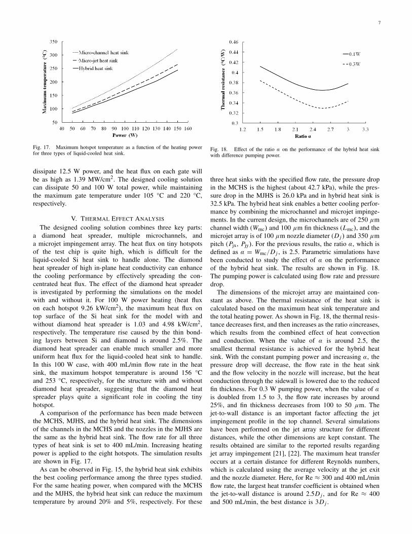
Fig. 17. Maximum hotspot temperature as a function of the heating powerfor three types of liquid-cooled heat sink.
dissipate 12.5 W power, and the heat flux on each gate willbe as high as 1.39 MW/cm2. The designed cooling solutioncan dissipate 50 and 100 W total power, while maintainingthe maximum gate temperature under 105 °C and 220 °C,respectively.
V. THERMAL EFFECT ANALYSIS
The designed cooling solution combines three key parts:a diamond heat spreader, multiple microchannels, anda microjet impingement array. The heat flux on tiny hotspotsof the test chip is quite high, which is difficult for theliquid-cooled Si heat sink to handle alone. The diamondheat spreader of high in-plane heat conductivity can enhancethe cooling performance by effectively spreading the con-centrated heat flux. The effect of the diamond heat spreaderis investigated by performing the simulations on the modelwith and without it. For 100 W power heating (heat fluxon each hotspot 9.26 kW/cm2), the maximum heat flux ontop surface of the Si heat sink for the model with andwithout diamond heat spreader is 1.03 and 4.98 kW/cm2,respectively. The temperature rise caused by the thin bond-ing layers between Si and diamond is around 2.5%. Thediamond heat spreader can enable much smaller and moreuniform heat flux for the liquid-cooled heat sink to handle.In this 100 W case, with 400 mL/min flow rate in the heatsink, the maximum hotspot temperature is around 156 °Cand 253 °C, respectively, for the structure with and withoutdiamond heat spreader, suggesting that the diamond heatspreader plays quite a significant role in cooling the tinyhotspot.
A comparison of the performance has been made betweenthe MCHS, MJHS, and the hybrid heat sink. The dimensionsof the channels in the MCHS and the nozzles in the MJHS arethe same as the hybrid heat sink. The flow rate for all threetypes of heat sink is set to 400 mL/min. Increasing heatingpower is applied to the eight hotspots. The simulation resultsare shown in Fig. 17.
As can be observed in Fig. 15, the hybrid heat sink exhibitsthe best cooling performance among the three types studied.For the same heating power, when compared with the MCHSand the MJHS, the hybrid heat sink can reduce the maximumtemperature by around 20% and 5%, respectively. For these
Fig. 18. Effect of the ratio α on the performance of the hybrid heat sinkwith difference pumping power.
three heat sinks with the specified flow rate, the pressure dropin the MCHS is the highest (about 42.7 kPa), while the pres-sure drop in the MJHS is 26.0 kPa and in hybrid heat sink is32.5 kPa. The hybrid heat sink enables a better cooling perfor-mance by combining the microchannel and microjet impinge-ments. In the current design, the microchannels are of 250 μmchannel width (Wmc) and 100 μm fin thickness (Lmc), and themicrojet array is of 100 μm nozzle diameter (D j ) and 350 μmpitch (Pjx, Pjy). For the previous results, the ratio α, which isdefined as α = Wmc/D j , is 2.5. Parametric simulations havebeen conducted to study the effect of α on the performanceof the hybrid heat sink. The results are shown in Fig. 18.The pumping power is calculated using flow rate and pressuredrop.
The dimensions of the microjet array are maintained con-stant as above. The thermal resistance of the heat sink iscalculated based on the maximum heat sink temperature andthe total heating power. As shown in Fig. 18, the thermal resis-tance decreases first, and then increases as the ratio αincreases,which results from the combined effect of heat convectionand conduction. When the value of α is around 2.5, thesmallest thermal resistance is achieved for the hybrid heatsink. With the constant pumping power and increasing α, thepressure drop will decrease, the flow rate in the heat sinkand the flow velocity in the nozzle will increase, but the heatconduction through the sidewall is lowered due to the reducedfin thickness. For 0.3 W pumping power, when the value of αis doubled from 1.5 to 3, the flow rate increases by around25%, and fin thickness decreases from 100 to 50 μm. Thejet-to-wall distance is an important factor affecting the jetimpingement profile in the top channel. Several simulationshave been performed on the jet array structure for differentdistances, while the other dimensions are kept constant. Theresults obtained are similar to the reported results regardingjet array impingement [21], [22]. The maximum heat transferoccurs at a certain distance for different Reynolds numbers,which is calculated using the average velocity at the jet exitand the nozzle diameter. Here, for Re ≈ 300 and 400 mL/minflow rate, the largest heat transfer coefficient is obtained whenthe jet-to-wall distance is around 2.5D j , and for Re ≈ 400and 500 mL/min, the best distance is 3D j .

8
Fig. 19. Thermal performances as a function of the pumping power for themicrojet array of different nozzle diameters.
The effect of the microjet diameter on the thermal perfor-mance of the heat sink is investigated with various drivingpressures. The jet array structure with nozzle diameters 80,100, and 120 μm is analyzed. The other dimensions of themicrochannels and microjets are assumed to be the same, asshown in Fig. 3. With the same pressure drop, the volume flowrate in the heat sink of smaller nozzle diameter will be smallerthan for the larger diameter. With the same ratio α, the largerdiameter will result in smaller fin thickness Lmc. Fig. 19 showsthat with the same pumping power, the thermal performanceof the heat sink can be improved by increasing the nozzlediameter. The effect is more pronounced when increasing thediameter from 80 to 100 μm, where the thermal resistancecan be reduced by 6.5%–11.8%. By increasing the nozzlediameter from 100 to 120 μm, only slightly improvementcan be achieved, which results due to the combined effect ofthe increased heat transfer coefficient and the weakened heatconduction through the fin. For the same flow rate, higherpressure drop will be required for the array of smaller nozzlediameter, which will result in high flow velocity from the exitof the jet. Although the jet velocity is lower for larger jetdiameter, a larger stagnation zone can be achieved for betterheat convection. For a 400 mL/min flow rate, for the jet arrayof 100 μm diameter the thermal resistance is 5.8% smallerthan that for 80 μm, and 7.4% smaller than that for 120 μm.The pressure drop required is much larger for the jet of 80 μmdiameter, which is around one and three times larger than thatfor the 100 and 120 μm diameter, respectively.
By decreasing the nozzle pitch, more microjets can beinvolved in the cooling area covered by the hybrid heat sink(5 × 6.5 mm2). To investigate this influence, the y-directionpitch Pjy (along the microchannel) is decreased from 3.5D j to2.5D j , and then the number of nozzles in each row increasesfrom 14 to 18. The microjets are still evenly located in18 columns in x-direction (across the microchannels). Thethermal performance and flow motion in the hybrid heat sinkare evaluated with the constant pumping power of 0.2 W. Forthis pumping power, the flow rate and pressure drop in array(a) is 400 mL/min and 30 kPa, and in array (b) is 416 mL/minand 29 kPa. Several microjets of Pjy = 2.5D j under the centerhotspot are shown in Fig. 20, compared with the microjets ofPjy = 3.5D j .
Fig. 20. Thermal performance and flow motion of the microjet array of(a) Pjy = 3.5D j , 14 × 18 and (b) Pjy = 2.5D j , 18 × 18. The color of theflow stream line represents the fluid temperature.
With 100-W heating power, the maximum hotspot temper-ature for the microjet array (a) is 156 °C, while that for array(b) is 153 °C. The heat dissipation capability of the heatsink can be slightly improved by using the array of smallerpitch and more nozzles. With the decreased pitch, the flowmotion of the jet might be negatively impacted by the adjacentjets, which results in a 31.9% decrease of the maximumlocal heat transfer coefficient. However, more microjets canbe located near the main hotspot heating area, which canenable 19.0% increase of the spatially averaged heat transfercoefficient.
VI. CONCLUSION
A direct-die-attached cooling solution with diamond heatspreader and hybrid Si heat sink has been developed forhotspot cooling. In the fabricated test chip, a hotspot of size450 × 300 μm2 is used to represent one GaN transistor with10 gate fingers. High heat flux, from 0.93 to 13.89 kW/cm2,is concentrated on the heater area in the thermal test chip.The hybrid Si heat sink combines the microchannel flowand the microjet array impingement, and are fabricated usingthe DRIE process and bonded through the TCB process.High heat dissipation capability of the direct-die-attachedstructure for hotspot cooling has been verified by perform-ing experiments and simulations. The submodel approachhas been used to predict the thermal performance of theGaN-on-Si device. With the flow rate of 400 mL/min andthe pressure drop of 30 kPa, high concentrated heat flux onthe Si thermal chip can be dissipated. A spatially averagedheat transfer coefficient of 11.53 × 10⁴ W/m2K is obtained,while the maximum local coefficient can be as high as 100 ×104 W/m2K. The cooling effects of the heat spreader, multiplemicrochannels, and microjet array are studied separately. Thecombination of all three cooling methods enables better heatremoval capability. The dimension effects of dimension

9
ratio α, jet-to-wall distance, nozzle diameter, and nozzle pitchhave been investigated. The results obtained in this paper areexpected to aid the design of cooling solutions for electronicdevices with hotspots.
REFERENCES
[1] A. J. Robinson, “A thermal–hydraulic comparison of liquid microchan-nel and impinging liquid jet array heat sinks for high-power electronicscooling,” IEEE Trans. Compon. Packag. Technol., vol. 32, no. 2,pp. 347–357, Jun. 2009.
[2] Y. Mizuno, I. Soga, S. Hirose, O. Tsuboi, and T. Iwai, “Si microchannelcooler integrated with high power amplifiers for base station of mobilecommunication systems,” in Proc. IEEE 61st Electron. Compon. Tech-nol. Conf. (EPTC), May/Jun. 2011, pp. 1541–1546.
[3] J. P. Calame, R. E. Myers, S. C. Binari, F. N. Wood, and M. Garven,“Experimental investigation of microchannel coolers for the high heatflux thermal management of GaN-on-SiC semicronductor devices,” Int.J. Heat Mass Transf., vol. 50, nos. 23–24, pp. 4767–4779, Nov. 2007.
[4] Y. J. Lee, B. L. Lau, Y. C. Leong, K. F. Choo, X. Zhang, andP. K. Chan, “GaN-on-Si hotspot thermal management using direct-die-attached microchannel heat sink,” in Proc. IEEE 14th Electron. Packag.Technol. Conf., Singapore, Dec. 2012, pp. 121–125.
[5] V. Sahu, Y. K. Joshi, K. Yazawa, A. G. Fedorov, S. Ali, and A. Ziabari,“Energy efficient liquid-thermoelectric hybrid cooling for hot-spotremoval,” in Proc. Annu. IEEE 28th Semicond. Thermal Meas. Manag.Symp. (SEMI-THERM), Mar. 2012, pp. 130–134.
[6] M. K. Sung and I. Mudawar, “Single-phase hybrid micro-channel/microjet impingement cooling,” Int. J. Heat Mass Transf., vol. 51,nos. 17–18, pp. 4342–4352, Aug. 2008.
[7] E. G. Colgan et al., “A practical implementation of silicon microchannelcoolers for high power chips,” IEEE Trans. Compon. Packag. Technol.,vol. 30, no. 2, pp. 218–225, Jun. 2007.
[8] M. Fabbri and V. K. Dhir, “Optimized heat transfer for high powerelectronic cooling using arrays of microjets,” J. Heat Transf., vol. 127,no. 7, pp. 760–769, Nov. 2004.
[9] S. Brunschwiler et al., “Direct liquid jet-impingement cooling withmicron-sized nozzle array and distributed return architecture,” in Proc.10th Intersoc. Conf. Thermal Thermomech. Phenomena Electron. Syst.(ITHERM), San Diego, CA, USA, 2006, pp. 196–203.
[10] M. K. Sung and I. Mudawar, “Effects of jet pattern on single-phase cooling performance of hybrid micro-channel/micro-circular-jet-impingement thermal management scheme,” Int. J. Heat Mass Transf.,vol. 51, nos. 19–20, pp. 4614–4627, Sep. 2008.
[11] J. P. Calame, R. E. Myers, F. N. Wood, and S. C. Binari, “Simulationof direct-die-attached microchannel coolers for the thermal managementof GaN-on-SiC microwave amplifiers,” IEEE Trans. Compon. Packag.Technol., vol. 28, no. 4, pp. 797–809, Dec. 2005.
[12] S. Subrina, D. Kotchetkov, and A. A. Balandin, “Heat removal in silicon-on-insultaor integrated circuit with graphene lateral heat spreader,” IEEEElectron Device Lett., vol. 30, no. 12, pp. 1281–1283, Dec. 2009.
[13] G. Maranzana, I. Perry, D. Maillet, and S. Rael, “Design optimization ofa spreader heat sink for power electronics,” Int. J. Thermal Sci., vol. 43,no. 1, pp. 21–29, Jan. 2004.
[14] S. Lee, S. Song, V. Au, and K. P. Moran, “Constriction/spreadingresistance model for electronics packaging,” in Proc. Thermal Eng. Conf.Austral. Soc. Music Educ. Jpn. Soc. Mech. Eng. (ASME-JSME), 1994,pp. 111–121.
[15] G. N. Ellison, “Maximum thermal spreading resistance for rectangularsources and plates with nonunity aspect ratios,” IEEE Trans. Compon.Packag. Technol., vol. 26, no. 2, pp. 439–454, Jun. 2003.
[16] P. Hui and H. S. Tan, “Three-dimensional analysis of a thermal dissipa-tion system with a rectangular diamond heat spreader on a semi-infinitecopper heat sink,” Jpn. J. Appl. Phys., vol. 35, no. 9A, pp. 4852–4861,1996.
[17] P. Hui, C. P. Tso, and H. S. Tan, “A rigorous series solution for diamondheat spreaders with temperature-dependent thermal conductivity usedin microwave power devices,” Jpn. J. Appl. Phys., vol. 35, no. 11,pp. 5796–5804, 1996.
[18] A. Rogacs and J. Rhee, “Performance-cost optimization of a diamondheat spreader,” in Proc. 12th Int. Symp. Adv. Packag. Mater., Process.Properties Interf. (APM), Oct. 2007, pp. 65–72.
[19] B. L. Lau, Y. L. Lee, Y. C. Leong, K. F. Choo, X. Zhang, andP. K. Chan, “Development of thermal test chip for GaN-on-Si devicehotspot characterization,” in Proc. IEEE 14th Electron. Packag. Technol.Conf. (EPTC), Dec. 2012, pp. 746–751.
[20] COMSOL Multiphyics Version 4.3a User Guide, COMSOL, Inc.,Burlington, MA, USA, Nov. 2012.
[21] H. O. Chang, “Liquid jet-array cooling modules for high heat fluxes,”Fluid Mech. Transp. Phenomena, vol. 44, no. 4, pp. 769–779, Apr. 1998.
[22] H. Sun, C. F. Ma, and W. Nakayama, “Local characteristic of convectiveheat transfer from simulated microelectric chips to impinging submergedround water jets,” J. Electron. Packag., vol. 115, no. 1, pp. 71–77,Mar. 1993.
Yong Han received the B.S. degree in electronicand information engineering from Shanxi University,Taiyuan, China, in 2004, and the Ph.D. degree inelectronic science and technology from the Instituteof Electronics of Chinese Academy of Sciences(IECAS), Beijing, China, in 2009.
He was an Assistant Researcher with the KeyLaboratory of High-Power Microwave Sources andTechnologies at IECAS after graduation. His scien-tific researches focused on the thermal, mechanical,and electromagnetic design and improvement of the
electronic systems. From 2011 to 2012, he was a Research Associate withthe Institute for Research in Electronics and Applied Physics, Universityof Maryland, College Park, MD, USA. His research concerned the theoryand the design of the microwave and millimeter-wave sources and thermalmanagement of the high-power electronic devices. Since 2012, he has been aResearch Scientist with the Institute of Microelectronics, Agency for Science,Technology and Research, Singapore. His current research interests include thecomputational modeling and thermal analysis, advanced microelectric systempackaging development, and electric cooling solutions.
Boon Long Lau received the B.S. degree fromthe National University of Singapore, Singapore, in2005.
He was with STMicroelectronics, Singapore, inthe field of process engineering after graduation.Since 2012, he has been with the Institute ofMicroelectronics, Agency for Science, Technologyand Research, Singapore. His current research inter-ests include microchannel and through-silicon-viaprocess integration.
Xiaowu Zhang (SM’10) received the B.S. degreein physics from the National University of DefenseTechnology, Changsha, China, in 1986, the M.E.degree in mechanics from the University of Scienceand Technology of China, Hefei, China, in 1989, andthe Ph.D. degree in mechanical engineering from theHong Kong University of Science and Technology,Hong Kong, in 1999.
He was a Lecturer with the Ballistic Research Lab-oratory of China, East China Institute of Technology,Nanjing, China, from 1989 to 1995. He has been
with the Institute of Microelectronics (IME), Agency for Science, Technologyand Research, Singapore, since 1999. He is currently a Principal Investigatorwith the Interconnection and Advanced Packaging Program at IME. Hehas authored and co-authored more than 120 technical papers in refereedjournals and conference proceedings. His current research interests includecomputational modeling and stress analysis, design for reliability, stresssensors, impact dynamics, advanced integrated circuit (IC) and microsystemspackaging development, and 3-D IC integration with through-silicon-viatechnology.

10
Yoke Choy Leong received the B.Eng. (Hons.)and M.Sc. degrees from the National University ofSingapore, Singapore, in 1991 and 1995, respec-tively, and the Ph.D. degree from the University ofMassachusetts at Amherst, Amherst, MA, USA, in2000.
He has been with DSO National Laborato-ries, Singapore, since 1991, where he is involvedin the area of microwave component and sys-tem design. His current research interests includemicrowave/monolithic microwave integrated circuit
design and modeling, analysis, and synthesis of novel passive structures.
Kok Fah Choo received the B.Sc (Hons.) degree inengineering (mechanical) from the Nanyang Tech-nological Institute/University, Singapore, in 1991.
He was with DSO National Laboratories, Singa-pore, from 1986 to 2002, progressing from a Tech-nical Officer to a Principal Member of TechnicalStaff and a Laboratory Head. In addition to manag-ing research and development projects at DSO, healso specializes in thermal design and analysis andelectronics packaging (module level), and is a co-inventor of a U.S. patent. Prior to joining Temasek
Laboratories (TL) at Nanyang Technological University, Singapore, he wasa Product Development Manager at D’Crypt Pte Ltd., Singapore, managingthe development of their cryptographic products and handling project andproduct management issues. He also concurrently managed operations atNuovoWave Pte Ltd., Singapore, a subsidiary of D’Crypt. He joined TL in2006. His current research interests include electronic cooling and packaging,in particular, high-heat dissipating devices.