Embed Size (px)
Citation preview
1 Low and Ultralow Dielectric Constant Films Prepared by Plasma-enhanced Chemical Vapor Deposition
A. Grill
IBM, T.J. Watson Research Center, Yorktown Heights, NY, USA
1.1 Introduction 1 1.2 Property Requirements for Integration 3 1.3 Characterization 4 1.4 Organic PECVD Dielectrics: Diamond-like Carbon
and Fluorinated Diamond-like Carbon 6 1.4.1 Preparation 6 1.4.2 Properties of DLC-type low-k dielectrics 7 1.4.3 Processing of DLC-type low-k dielectrics 12 1.4.4 Integration of DLC-type low-k dielectrics 14 1.4.5 Summary 15 1.5 SiCOH Films as Low-k and Ultralow-k Dielectrics 15 1.5.1 Preparation 16 1.5.2 Properties of SiCOH and pSiCOH dielectrics 18 1.5.3 Integration of SiCOH as the interconnect
dielectric 29 1.6 Conclusions 30 Addendum 30 References 30
1.1 INTRODUCTION
The semiconductor industry has been improving the performance of ultra-large-scale inte-grated (ULSI) circuits by shrinking the transistor size according to Moore’s Law, which states that the chip performance will double about every 18 months. The shrinking of the devices has resulted in increased device speed and device density. The speed of an electrical signal in an ULSI circuit is controlled by the switching time of the individual transistors
Dielectric Films for Advanced Microelectronics Edited by M. Baklanov, M. Green and K. Maex.© 2007 John Wiley & Sons, Ltd
COPYRIG
HTED M
ATERIAL
2 DIELECTRIC FILMS FOR ADVANCED MICROELECTRONICS
and by the signal propagation time through the interconnect system. The function of an interconnect or wiring system (also often referred to as the back end of the line, or BEOL) is to distribute the signals between the active devices and to provide power to and among the various circuit functions on a chip.
The signal delay of the BEOL is defi ned by its RC, R being the wire resistance and C the intralevel and interlevel dielectric capacitance. At a certain metallization level this is roughly dependent on
RC = 2rk(4L2/P2 + L2/T 2)
where L is the line length, P the metal pitch, T the metal line thickness, r the metal resis-tivity and k the dielectric constant of the insulator between the lines. Reducing the capaci-tance of the interconnect by replacing the dielectric with a material of lower k also reduces the power consumption of the circuit which is given by:
Power = CV 2f
where C is the capacitance of the circuit, and V and f are the operating voltage and frequency.
Each shrinking of the ULSI chips, which reduced the dimensions of the electrical devices, resulted in a reduced switching time of the transistors, but also caused a corre-sponding reduction in P and T, thus increased RC delays of the electrical signals. Thus, while the signal propagation time was much smaller than the switching time for many device generations, at a certain technology generation, the signal propagation though the interconnect structure became slower than the switching time of the active devices and it became necessary to reduce the RC delay of the BEOL for maintaining the high perform-ance of the ULSI semiconductor chips.
The Interconnect chapter of the 1994 National Technology Roadmap for Semiconductors (NTRS) was the fi rst to point out the need for new conductor and dielectric materials in order to meet the projected overall technology requirements.
A signifi cant improvement in the performance of the BEOL was achieved by replacing the Al interconnects with Cu, which has ∼30% lower resistivity than that of Al. The use of Cu as the BEOL metal was fi rst demonstrated by IBM and Motorola [1, 2] by 1998, and has been generally adopted afterwards by the entire semiconductor industry. The Cu metal-lization was introduced while still using silicon dioxide with a dielectric constant k of about 4 as the insulator dielectric. Further reduction of the signal delay in the BEOL required the replacement of the insulator with materials having lower dielectric constants.
Fluorinated silicon glass (FSG, or SiOF) was the fi rst dielectric with reduced dielectric constant (k = 3.7) to replace silicon oxide as the BEOL dielectric with Cu metallization at the 180 nm technology node [3].
However, the continuation of the decreasing of the dielectric constant of the insulator as predicted by the International Technology Roadmap for Semiconductors (ITRS) has been problematic. The reliability and yield issues associated with the integration of new dielectric materials with dual damascene copper processing proved to be much more challenging than initially predicted. According to ITRS, 1997 edition [4] it was expected that insulating materials with k = 2.5–3.0 will be introduced already at the 180 nm node in 1999. This prediction then shifted to the introduction of such materials at the 130 nm, to be fi nally
LOW AND ULTRALOW DIELECTRIC CONSTANT FILMS PREPARED 3
introduced only at the 90 nm node. Only the 2004 update of ITRS did not change the roadmap’s low-k portion, for the fi rst time in 10 years [5].
A large number of potential materials with low dielectric constants have been investi-gated over the years and details about these materials and their methods of fabrication and integration can be found in proceedings of MRS symposia [6] or ECS symposia [7] on low-k materials. In spite of the very large effort invested over many years by the semicon-ductor industry to replace the SiO2 and SiOF dielectrics with materials having signifi cantly lower dielectric constants, with about 150 different dielectric materials being identifi ed by SEMATECH in the mid-1990s [8], the practical progress in implementation of new dielec-trics has been delayed by 2001 up to four years relative to initial SIA roadmap projections. The delay was marked by continuous revisions outwards in time of SIA projections since 1997 [9].
The delay in the implementation of low-k dielectrics in ULSI interconnect structures was caused by their inability to satisfy the requirements of integration processing, as dis-cussed later and by their mechanical weakness compared with SiO2 and SiOF.
Most of the initial candidate low-k materials, organic polymers or hybrid, organosilicate glasses, were prepared by spin-on techniques. The dielectrics that will be discussed in this chapter are prepared by PECVD, although they are often mistakenly referred to as CVD fi lms. In CVD, or chemical vapor deposition, the deposition of the fi lm and its properties are controlled by the temperature of the substrate and the deposition process takes place under thermodynamic equilibrium and the fi lm has a well-defi ned structure and is usually crystalline (single crystal or polycrystalline).
In contrast to CVD, the PECVD (plasma enhanced CVD) method [10] is a nonequilib-rium technique, where the process is controlled mainly by the energy of the electrons in the plasma. The energy of the electrons in a plasma is defi ned by an average energy but is has a Druyvesteyn-type distribution with a tail extending to energies much larger than the average one [10]. As a result, the plasma dissociates the molecules in the gas phase into a variety of radicals, which recombine on the substrate to form a solid fi lm comprising a variety of different bonds. The fi lms deposited by PECVD are usually amorphous materials. The substrate temperature may affect the properties of the deposited fi lm, but it is typically lower than the one required to deposit a fi lm from the gas phase by thermal CVD.
1.2 PROPERTY REQUIREMENTS FOR INTEGRATION
As mentioned in the previous section, a large number of materials with low k values have been identifi ed over the years. However the implementation of such materials in a BEOL interconnect structure proved to be a very diffi cult task. In order to introduce a new dielec-tric as the insulator of the BEOL, the material has to satisfy a large number of criteria imposed by its functionality in the structure and by the integration processing. Some of these criteria are listed next [3, 11, 12]:
1. Electrical—to make it useful as a low-k insulator• low dielectric constant• low dissipation factor• low leakage currents at operating fi elds• high breakdown voltage
4 DIELECTRIC FILMS FOR ADVANCED MICROELECTRONICS
2. Thermal—to enable it withstand other integration processes• stability at temperatures greater than or equal to 400°C
3. Mechanical—to enable the fabrication of mechanically robust devices• maximal elastic (Young’s) modulus and hardness (to withstand harsh integration
processes, such as chemomechanical polishing (CMP), or assembly/packaging)• low stresses (to prevent cracking or delamination from other layers in the BEOL
structure),
4. Environmental stability• low moisture absorption• maintain electrical and mechanical properties under exposure to environment
5. Adhesion to and compatibility with other dielectrics (hardmask, caps, etch stops) or conductors (metal or nitride liners) in contact with it
6. Low/no oxygen and moisture diffusion through fi lm• prevent oxidation of the metallization materials, especially Cu
7. Solvent resistance—to maintain its properties after exposure to wet cleans during the integration processing
8. Patternability, etching at required dimensions• high etch selectivity during RIE processing
9. Chemomechanical polishing (CMP) capability and compatibility• maintain properties after exposure to CMP slurries
10. Avoid resist poisoning
11. No/minimal damage to dielectric by the integration processes
12. Commercial availability of precursors with reasonable shelf life
13. Low cost of fabricated fi lm
14. Environmental compliance of precursors and processing by-products.
The requirements listed above were fulfi lled by the classic dielectric SiO2, however most materials with lower k considered for replacing the oxide did fail many of these criteria and were removed from considerations. Even the low-k dielectrics that have fi nally been inte-grated in ULSI chips may not fulfi ll all the requirements listed above and the integration processes had to be modifi ed to accommodate for the lack of those.
1.3 CHARACTERIZATION
This section presents the characterization techniques used for the determination of the material properties of low-k dielectrics, for evaluating their potential suitability as the die-lectric of the interconnect of a ULSI. These characterizations will only evaluate the poten-tial of a candidate material, the fi nal suitability being established by the integration process, which is beyond the scope of this chapter.

LOW AND ULTRALOW DIELECTRIC CONSTANT FILMS PREPARED 5
The rest of the chapter will be separated between the discussion of organic, diamond-like carbon (DLC)-based fi lms and the discussion of the hybrid SiCOH fi lms. As the same characterization techniques are common for all types of dielectrics, these techniques will be discussed briefl y here. Some characterization techniques will be discussed in detail in the following chapters of this book.
The low-k fi lms were characterized as deposited and after thermal anneals. These anneals were performed for 4 h in an inert ambient either at 400 or 430°C.
The composition of the dielectric fi lms was determined by Rutherford backscattering (RBS) in combination with forward recoil elastic scattering (FRES), the latter being used for the determination of the hydrogen content. Both RBS and FRES data were analyzed in our studies with a RUMP program [13], which was used to simultaneously fi t theoretical fi lm compositions to both RBS and FRES experimental spectra in the same time.
Optical properties of the dielectric fi lms were determined by ellipsometry, Fourier trans-form infrared spectroscopy (FTIR) and n&k measurements [14]. The FTIR spectra were collected using the same substrate, from which the fi lm was removed, as the background. In most of the cases the collected spectra were baseline corrected. FTIR absorption peaks enable the identifi cation of the different bond structures in the fi lms. In some cases, peaks were deconvoluted into individual components to get a better understanding of the fi lm structure [15]. FTIR analysis can also be used to follow modifi cations in the fi lms as a result of processing of the dielectric or its exposure to the environment, but only if such changes are larger than a few percent.
The index of refraction n is often used to characterize dielectric fi lms due to its rela-tion to the dielectric constant (n2 k, the < sign stemming from the fact the n and k are usually measured at very different frequencies). The index of refraction can be deter-mined by ellipsometry if the thickness of the fi lm is known. The n&k tool enables simultaneous measurement of both fi lm thickness and n values over a wavelength range of 193–800 nm.
The dielectric constants were measured at 1 MHz, on metal–insulator–metal (MIS) structures using highly doped Si wafer substrates with mΩ resistivities. The low-k fi lms were deposited as blanket layers and the Al or Cu dots were deposited as metal contacts to the fi lm. The backside of the Si wafer was coated with an Al fi lm for improved electrical contact. Details of the electrical characterization techniques can be found elsewhere [16,
17]. The same structures were used to determine the leakage currents through the fi lms by measuring the I–V characteristics through contact dots of known area.
The stresses in the fi lms have been determined from the radius of curvature induced on the substrate by the deposited fi lm using the equation
σν
=−( )Eh
Rt
2
1 6
where s is the stress, E/(1-n) is the biaxial elastic modulus of the substrate (180 GPa for (100) Si wafers), h is the substrate thickness, t is the fi lm thickness, and R is the radius of curvature.
The elastic modulus E and hardness H of the fi lms were measured by nanoindentation. The measurements were done on 1 µm and >3 µm-thick fi lms. Despite the general belief that 1 µm fi lms are suffi cient for this characterization, it was found that at this thickness
6 DIELECTRIC FILMS FOR ADVANCED MICROELECTRONICS
the substrate effect was still signifi cant. That effect was eliminated by measuring fi lms at least 3 µm thick [18]. The cracking propensity of the fi lms and the critical thickness for crack development were determined by a technique described elsewhere [19].
Thickness changes resulting from different processes undergone by the dielectric fi lms were determined by measuring the height of steps etched in the fi lms using profi lometric techniques, or by comparing the thicknesses determined by n&k measurements before and after a certain process. Thickness changes have sometimes also been evaluated from changes in the FTIR peak intensity of the CHi absorption band of DLC fi lms (centered at 2920 cm−1 [17]) or the CFj absorption band of fl uorinated DLC (FDLC) fi lms (centered at about 1200 cm−1 [20]). This technique is estimating material loss from the fi lm rather than shrinkage.
The porosity of porous low-k and ultralow-k fi lms was characterized by several methods: ellipsometric porosimetry (EP), positron annihilation spectroscopy (PAS) and positron annihilation lifetime spectroscopy (PALS), small-angle X-ray scattering (SAXS), and spec-ular X-ray refl ectivity. The techniques enable the determination of the degree of porosity in the fi lms and the pore size distribution (PSD). A description of the different techniques with further references to the details of the used methods can be found in references [21–23]. A detailed description is provided in Chapter 3 of this book.
1.4 ORGANIC PECVD DIELECTRICS: DIAMOND-LIKE CARBON AND FLUORINATED DIAMOND-LIKE CARBON
Diamond-like carbon (DLC) and its modifi cations were the fi rst low-k dielectrics prepared by PECVD. DLC is an amorphous hydrogenated carbon that can be easily modifi ed to incorporate additional elements in its amorphous structure. Among such elements, F, Si, or metals have been incorporated in DLC to modify its tribological behavior [17, 24]. For its potential use as a low-k dielectric, F-containing (fl uorinated DLC, or FDLC) and Si-containing DLC (SiDLC) have been considered. The preparation of the different types of fi lms will be described next.
1.4.1 Preparation
Low-k DLC fi lms have been prepared by RF PECVD in a parallel plate reactor, at pressures of 100–300 mTorr and RF powers of 25–100 W, corresponding to power densities of 0.08–0.31 W/cm2, as described in detail elsewhere [25, 26]. The RF plasma was sustained with a RF power supply at a frequency of 13.56 MHz. The growth rate and properties of DLC fi lms are controlled by the substrate bias during deposition [17]; therefore the deposition was performed on substrates placed on the powered electrode, thus being at a negative self-bias. For the range of used plasma conditions, the substrate bias was in the range −80 to −300 V DC.
The deposition of DLC was performed at substrate temperatures below 250°C, because deposition at higher temperatures causes the formation of fi lms with more graphite-like than diamond-like characteristics [17] and such fi lms are characterized by high current leakage and high k values. The precursor for the deposition of DLC fi lms can be any pure hydrocarbon, such as methane, acetylene, cyclohexane.
LOW AND ULTRALOW DIELECTRIC CONSTANT FILMS PREPARED 7
FDLC fi lms, generally characterized by lower dielectric constants then DLC, have been deposited from fl uorocarbons, mixtures of fl uorocarbons with hydrogen, or mixtures of fl uorocarbons with hydrocarbons, using parallel plate RF PECVD reactors [26, 27] or high-density plasma reactors [28, 29]. Contrary to DLC, low-k FDLC fi lms can be deposited at temperatures up to 400°C and on either electrode of the parallel plate reactor.
1.4.2 Properties of DLC-type low-k dielectrics
DLC
DLC and FDLC have been considered as potential low-k dielectrics as early as 1995, but the fi rst reported fi lms were either not stable above 300°C [30, 31], or had dielectric con-stants of about 6 [32]. In 1997 we reported for the fi rst time low-k DLC fi lms stable up to 400°C [25] and FDLC fi lms with k = 2.3 have been reported elsewhere [27].
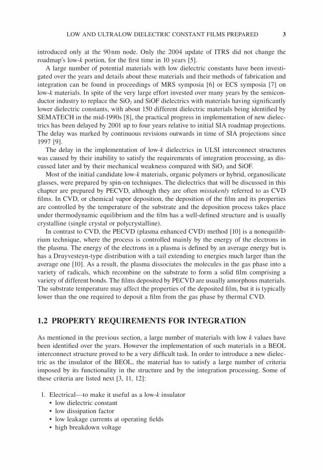
The low-k DLC fi lms contained 40–46% hydrogen, the amount of hydrogen decreasing with increasing RF power and decreasing pressure during deposition [25]. The dielectric constant of DLC displayed an opposite behavior, decreasing with decreasing RF power and increasing pressures as illustrated in Figure 1.1. The dielectric constant could be lowered, within the range of investigated deposition parameters, from 3.9 to values as low as 2.7. The same data from Figure 1.1 is presented as a function of the substrate bias during depo-sition in Figure 1.2 [33], where it can be seen that the dielectric constant of DLC fi lms prepared from one precursor is essentially controlled by the substrate bias and decreases with decreasing bias.
DLC fi lms, generally developed for tribological applications, are usually characterized by high internal compressive stresses [17]. The stress of DLC fi lms deposited for low-k applications was found to be essentially controlled by the substrate bias during fi lm deposi-tion, similar to the dielectric constant [33]. The compressive stress in the as-deposited fi lms
20 40 60 80 1002.0
2.4
2.8
3.2
3.6
4.0
100 mtorr 200 mtorr 300 mtorr
Die
lect
ric c
onst
ant
Power (W)
Figure 1.1 Dielectric constant of as-deposited DLC as a function of RF power at different deposi-tion pressures (Reprinted with permission from [25] Copyright 1997 Materials Research Society)

8 DIELECTRIC FILMS FOR ADVANCED MICROELECTRONICS
could be reduced from about 800 MPa to about 200 MPa by decreasing the RF power and increasing the deposition pressure, or decreasing the bias. Thus, the DLC fi lms having lower k values are also characterized by lower intrinsic stresses. This appeared to be a benefi cial trend, as high intrinsic stress can be detrimental to the manufacturing process if such fi lms could be used as the BEOL dielectric in ULSI circuits. High fi lm stresses can cause wafer bowing and interfere with the patterning process, as well as causing stress-related adhesion failure. However, we shall see in the following that the as-deposited, low-k, low-stress fi lms were not stable at 400°C.
Figure 1.3 [26] presents the thickness changes caused by the annealing at 400°C for 4 h in an inert ambient and the stresses in the as-deposited DLC fi lms as a function of the dielec-
80 120 160 200 240 280 3202.6
2.8
3.0
3.2
3.4
3.6
3.8
4.0
Die
lect
ric c
onst
ant
Bias (-V)
100 mtorr 200 mtorr 300 mtorr
Figure 1.2 Dielectric constants of DLC vs substrate bias during deposition (Reprinted from [33] with permission from Elsevier)
2.6 2.8 3.0 3.2 3.4 3.6 3.8 4.0-80
-60
-40
-20
0
20
Dielectric constant
Thi
ckne
ss c
hang
e (%
)
D.th
0
200
400
600
800
1000
1200
Stress (M
Pa)
Stress
Figure 1.3 Thickness change after annealing and stress in as-deposited DLC vs dielectric constant of as deposited fi lm (Reprinted with permission from [26] Copyright 1997 Materials Research Society)
LOW AND ULTRALOW DIELECTRIC CONSTANT FILMS PREPARED 9
tric constant of the as-deposited fi lms. It can be seen that fi lms having a dielectric constant higher than about 3.3 have high intrinsic stresses and are characterized by a small increase in fi lm thickness after annealing. In contrast, fi lms having lower dielectric constants have smaller intrinsic stresses, but lose a high fraction of their thickness during annealing. The similar dependence of dielectric constant, hydrogen content, stress, and thermal stability of DLC fi lms on the deposition conditions may be explained by the effect of the deposition conditions on the fi lm structure. DLC fi lms are amorphous cross-linked structures, whose degree of cross-linking and carbon hybridization, sp2, sp3, depends on the ion bombardment of the growing fi lms [17]. Higher powers and/or lower pressures in the plasma (lower substrate bias) result in incorporation of smaller amounts of hydrogen and stronger cross-linking in the fi lms, producing fi lms of higher thermal stability characterized by higher dielectric constants and higher stresses.
It is apparent from the discussion above that it might be possible to deposit DLC fi lms with suffi cient thermal stability at 400°C, however the required deposition conditions produce fi lms with dielectric constants higher then 3.3. As-deposited DLC fi lms of lower dielectric constants and lower stresses are not stable at this thermal exposure [26]. Never-theless, it has been found that DLC fi lms having dielectric constants as low as 2.7 can be stabilized by annealing them fi rst in a nonoxidizing ambience at the highest temperature dictated by the integration processes [12, 33]. Subsequent anneals at the same temperature did not modify the fi lms any more. Furthermore, the stresses in the DLC fi lms decreased after annealing from the as-deposited compressive stress of about 500 MPa and, for fi lms with k = 2.7, the stress became slightly tensile.
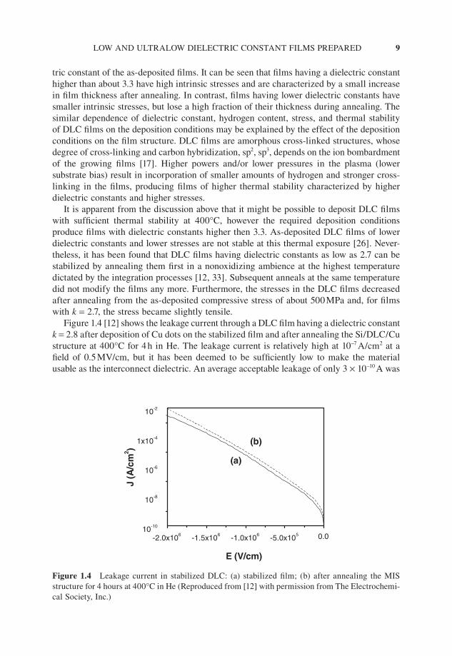
Figure 1.4 [12] shows the leakage current through a DLC fi lm having a dielectric constant k = 2.8 after deposition of Cu dots on the stabilized fi lm and after annealing the Si/DLC/Cu structure at 400°C for 4 h in He. The leakage current is relatively high at 10−7 A/cm2 at a fi eld of 0.5 MV/cm, but it has been deemed to be suffi ciently low to make the material usable as the interconnect dielectric. An average acceptable leakage of only 3 × 10⁻¹⁰ A was
-2.0x10⁶ -1.5x10⁶ -1.0x10⁶ -5.0x10⁵ 0.010-10
10-8
10-6
1x10⁻⁴
10-2
(a)
(b)
J (A
/cm
2 )
E (V/cm)
Figure 1.4 Leakage current in stabilized DLC: (a) stabilized fi lm; (b) after annealing the MIS structure for 4 hours at 400°C in He (Reproduced from [12] with permission from The Electrochemi-cal Society, Inc.)

10 DIELECTRIC FILMS FOR ADVANCED MICROELECTRONICS
measured at 1.8 V in an integrated a Cu serpentine 3.8 m long, separated from an adjacent comb structure by 0.34 µm of DLC [34]. The repeated annealing at 400°C of the stabilized fi lms induced only a small increase in the leakage current trough the DLC fi lm.
FDLC
Claims have been made that FDLC fi lms can be prepared to be stable at 400°C [11, 27, 35]. Such FDLC fi lms were also characterized by low internal compressive stresses of about 150 MPa in as-deposited conditions and decreased further after annealing [11].
FDLC fi lms deposited from the pure fl uorocarbon precursor (hexafl uorobenzene) had fl uorine concentrations up to 42%, which where almost constant for a large range of deposi-tion conditions [11]. The fl uorine is mostly bound in CF2 and CF3 bonds in such fi lms [20]. Such fl uorine concentration in the fi lms was considered to be too high, raising concerns about possible reactions of F with the materials in contact with the FDLC layers in the BEOL interconnect structure. Hydrogen dilution of the precursor in the plasma was used to reduce the F content and, for a range of investigated mixtures, the fl uorine concentration in the fi lms could be decreased to 20% with a concomitant increase of the hydrogen con-centration up to 12% [11].
The dielectric constants of as-deposited FDLC fi lms are presented in Figure 1.5 [25] as a function of hydrogen dilution of the fl uorocarbon precursor, at different RF powers sup-plied to the plasma. As can be seen, FDLC fi lms deposited from pure fl uorocarbon have dielectric constants as low as 2.55. Dilution of the fl uorocarbon precursor with hydrogen increased the dielectric constant of the fi lms, due to the replacement of fl uorine with hydro-gen in the fi lms. The deposition power had a similar effect on the dielectric constant, which increased with increasing deposition power. Dielectric constants as low as 2.3 have been reported by other groups [27, 28].
0 1 2 32.4
2.6
2.8
3.0
3.2
RF Power
16 W 22 W 40 W 95 W 70 W 85 W 66 W 91 W
Die
lect
ric c
onst
ant
H2/C
6F
6
Figure 1.5 Dielectric constant of as-deposited FDLC fi lms as a function of the precursor dilution with hydrogen (Reprinted with permission from [25] Copyright 1997 Materials Research Society)
LOW AND ULTRALOW DIELECTRIC CONSTANT FILMS PREPARED 11
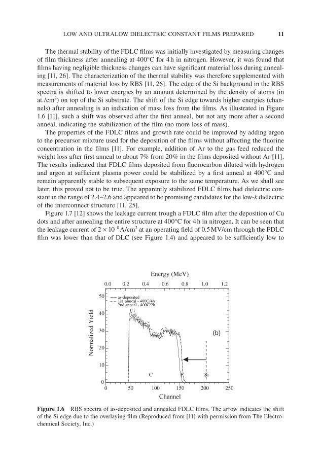
The thermal stability of the FDLC fi lms was initially investigated by measuring changes of fi lm thickness after annealing at 400°C for 4 h in nitrogen. However, it was found that fi lms having negligible thickness changes can have signifi cant material loss during anneal-ing [11, 26]. The characterization of the thermal stability was therefore supplemented with measurements of material loss by RBS [11, 26]. The edge of the Si background in the RBS spectra is shifted to lower energies by an amount determined by the density of atoms (in at./cm2) on top of the Si substrate. The shift of the Si edge towards higher energies (chan-nels) after annealing is an indication of mass loss from the fi lms. As illustrated in Figure 1.6 [11], such a shift was observed after the fi rst anneal, but not any more after a second anneal, indicating the stabilization of the fi lm (no more loss of mass).
The properties of the FDLC fi lms and growth rate could be improved by adding argon to the precursor mixture used for the deposition of the fi lms without affecting the fl uorine concentration in the fi lms [11]. For example, addition of Ar to the gas feed reduced the weight loss after fi rst anneal to about 7% from 20% in the fi lms deposited without Ar [11]. The results indicated that FDLC fi lms deposited from fl uorocarbon diluted with hydrogen and argon at suffi cient plasma power could be stabilized by a fi rst anneal at 400°C and remain apparently stable to subsequent exposure to the same temperature. As we shall see later, this proved not to be true. The apparently stabilized FDLC fi lms had dielectric con-stant in the range of 2.4–2.6 and appeared to be promising candidates for the low-k dielectric of the interconnect structure [11, 25].
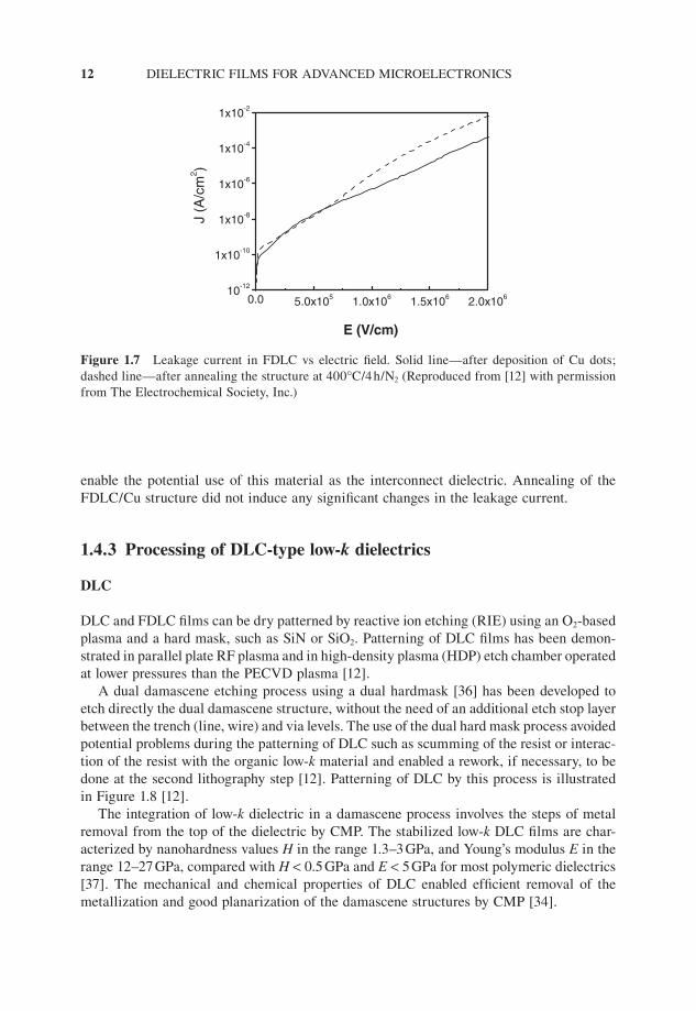
Figure 1.7 [12] shows the leakage current trough a FDLC fi lm after the deposition of Cu dots and after annealing the entire structure at 400°C for 4 h in nitrogen. It can be seen that the leakage current of 2 × 10⁻⁸ A/cm2 at an operating fi eld of 0.5 MV/cm through the FDLC fi lm was lower than that of DLC (see Figure 1.4) and appeared to be suffi ciently low to
0 50 100 150 200 250
Channel
0
10
20
30
40
50
Nor
mal
ized
Yie
ld
0.0 0.2 0.4 0.6 0.8 1.0 1.2
Energy (MeV)
as-deposited1st anneal - 400C/4h2nd anneal - 400C/2h
C SiF
(b)
Figure 1.6 RBS spectra of as-deposited and annealed FDLC fi lms. The arrow indicates the shift of the Si edge due to the overlaying fi lm (Reproduced from [11] with permission from The Electro-chemical Society, Inc.)
12 DIELECTRIC FILMS FOR ADVANCED MICROELECTRONICS
enable the potential use of this material as the interconnect dielectric. Annealing of the FDLC/Cu structure did not induce any signifi cant changes in the leakage current.
1.4.3 Processing of DLC-type low-k dielectrics
DLC
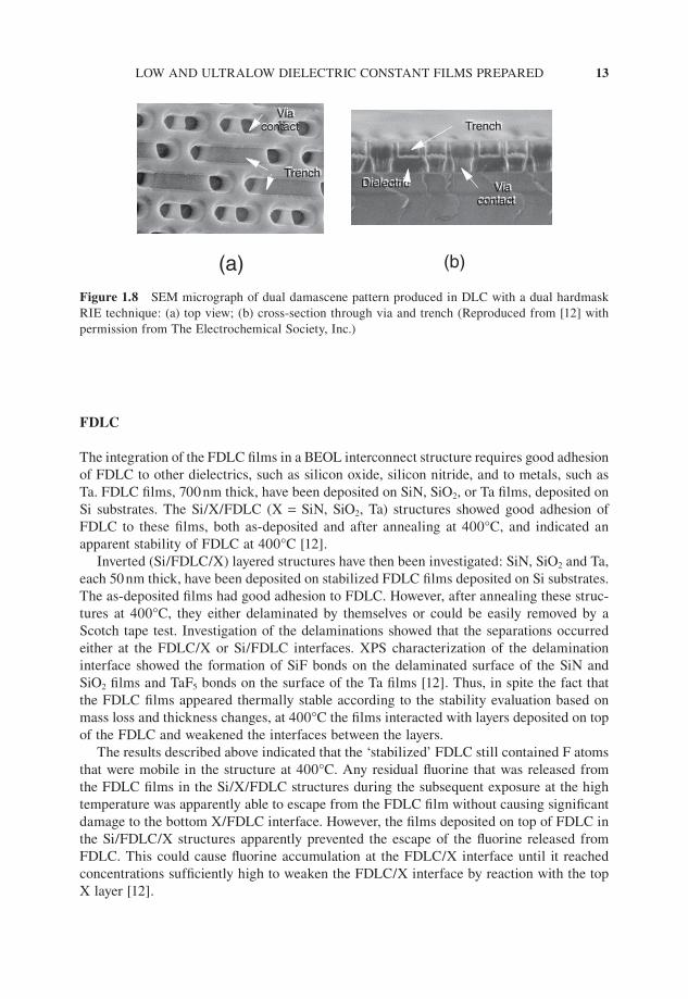
DLC and FDLC fi lms can be dry patterned by reactive ion etching (RIE) using an O2-based plasma and a hard mask, such as SiN or SiO2. Patterning of DLC fi lms has been demon-strated in parallel plate RF plasma and in high-density plasma (HDP) etch chamber operated at lower pressures than the PECVD plasma [12].
A dual damascene etching process using a dual hardmask [36] has been developed to etch directly the dual damascene structure, without the need of an additional etch stop layer between the trench (line, wire) and via levels. The use of the dual hard mask process avoided potential problems during the patterning of DLC such as scumming of the resist or interac-tion of the resist with the organic low-k material and enabled a rework, if necessary, to be done at the second lithography step [12]. Patterning of DLC by this process is illustrated in Figure 1.8 [12].
The integration of low-k dielectric in a damascene process involves the steps of metal removal from the top of the dielectric by CMP. The stabilized low-k DLC fi lms are char-acterized by nanohardness values H in the range 1.3–3 GPa, and Young’s modulus E in the range 12–27 GPa, compared with H < 0.5 GPa and E < 5 GPa for most polymeric dielectrics [37]. The mechanical and chemical properties of DLC enabled effi cient removal of the metallization and good planarization of the damascene structures by CMP [34].
0.0 5.0x10⁵ 1.0x10⁶ 1.5x10⁶ 2.0x10610-12
1x10⁻¹⁰
1x10⁻⁸
1x10⁻⁶
1x10⁻⁴
1x10⁻²
E (V/cm)
J (A
/cm
2 )
Figure 1.7 Leakage current in FDLC vs electric fi eld. Solid line—after deposition of Cu dots; dashed line—after annealing the structure at 400°C/4 h/N2 (Reproduced from [12] with permission from The Electrochemical Society, Inc.)
LOW AND ULTRALOW DIELECTRIC CONSTANT FILMS PREPARED 13
FDLC
The integration of the FDLC fi lms in a BEOL interconnect structure requires good adhesion of FDLC to other dielectrics, such as silicon oxide, silicon nitride, and to metals, such as Ta. FDLC fi lms, 700 nm thick, have been deposited on SiN, SiO2, or Ta fi lms, deposited on Si substrates. The Si/X/FDLC (X = SiN, SiO2, Ta) structures showed good adhesion of FDLC to these fi lms, both as-deposited and after annealing at 400°C, and indicated an apparent stability of FDLC at 400°C [12].
Inverted (Si/FDLC/X) layered structures have then been investigated: SiN, SiO2 and Ta, each 50 nm thick, have been deposited on stabilized FDLC fi lms deposited on Si substrates. The as-deposited fi lms had good adhesion to FDLC. However, after annealing these struc-tures at 400°C, they either delaminated by themselves or could be easily removed by a Scotch tape test. Investigation of the delaminations showed that the separations occurred either at the FDLC/X or Si/FDLC interfaces. XPS characterization of the delamination interface showed the formation of SiF bonds on the delaminated surface of the SiN and SiO2 fi lms and TaF5 bonds on the surface of the Ta fi lms [12]. Thus, in spite the fact that the FDLC fi lms appeared thermally stable according to the stability evaluation based on mass loss and thickness changes, at 400°C the fi lms interacted with layers deposited on top of the FDLC and weakened the interfaces between the layers.
The results described above indicated that the ‘stabilized’ FDLC still contained F atoms that were mobile in the structure at 400°C. Any residual fl uorine that was released from the FDLC fi lms in the Si/X/FDLC structures during the subsequent exposure at the high temperature was apparently able to escape from the FDLC fi lm without causing signifi cant damage to the bottom X/FDLC interface. However, the fi lms deposited on top of FDLC in the Si/FDLC/X structures apparently prevented the escape of the fl uorine released from FDLC. This could cause fl uorine accumulation at the FDLC/X interface until it reached concentrations suffi ciently high to weaken the FDLC/X interface by reaction with the top X layer [12].
Via Via contact contact
Trench Trench Via Via
contact contact
Trench Trench
DielectricDielectric
(b)(a)
Figure 1.8 SEM micrograph of dual damascene pattern produced in DLC with a dual hardmask RIE technique: (a) top view; (b) cross-section through via and trench (Reproduced from [12] with permission from The Electrochemical Society, Inc.)

14 DIELECTRIC FILMS FOR ADVANCED MICROELECTRONICS
1.4.4 Integration of DLC-type low-k dielectrics
DLC
The fi rst stage of integration of DLC low-k dielectric with copper metallization is illus-trated in Figure 1.9 for a fi rst metallization M1 interconnect level [12]. The fi gure shows the cross-section of the Cu wires embedded in a fi rst level DLC dielectric coated with a yet unpatterned V1 level DLC layer on top of it. The illustrated structure incorporates a SiN diffusion cap layer on top of the DLC level. The micrograph illustrates the integrity of the structure.
A further step of integration of DLC with copper metallization is illustrated in Figure 1.10 [33]. The fi gure shows the cross-section of two levels of Cu wires embedded in three levels of DLC dielectric. The M2 Cu wires have an imperfect shape because the etching process of
1 micron
DLC V1
DLC M1
Cu M1
SiN cap
Figure 1.9 SEM micrograph of a cross-section of a M1 Cu/DLC integrated structure (Reproduced from [12] with permission from The Electrochemical Society, Inc.)
DLC
Cu
PSG
M1
V1
M2
V2M3
Figure 1.10 SEM micrograph of a two-level Cu/DLC integrated structure (Reprinted from [33] with permission from Elsevier)

LOW AND ULTRALOW DIELECTRIC CONSTANT FILMS PREPARED 15
the DLC was not yet optimized for the patterned structure on 8-inch wafers. Nevertheless, the micrograph illustrates the integrity of the structure up to the third DLC level V2M3. Initial electrical evaluation of 8-inch wafers have shown signifi cant yields for both opens and shorts measurements. These results indicated the potential of DLC as a candidate for use as a low-k interconnect dielectric with Cu metallization in the BEOL of ULSI chips.
FDLC
It was shown above that the FDLC fi lms were not stable enough to prevent release of fl uorine and its interactions with other layers in contact with it during exposure at 400°C. While other authors claimed to have fabricated FDLC fi lms thermally stable at 400°C [11, 27, 35], the stability of these materials has not been proven by integration with other fi lms at this temperature. Initial integration of FDLC with Al in a gap fi ll process [28] and with Cu in a damascene process [29] has been demonstrated only to temperatures below 350°C.
1.4.5 Summary
The results discussed above showed that it is possible to prepare by PECVD hydrogenated (DLC) and fl uorinated (FDLC) amorphous carbon fi lms with dielectric constants as low as 2.7 for DLC and 2.3 for FDLC. DLC fi lms with low k values could be stabilized by anneal-ing them at 400°C.
The stabilization of FDLC by such an anneal proved to be only apparent. The annealed fi lms seem to contain suffi cient mobile fl uorine that can interact with the adjacent layers at 400°C and weaken the interfaces. As a result FDLC did not seem to be a good candidate for use as the interconnect low-k dielectric.
Stabilized DLC fi lms, with dielectric constants k < 3.0, have shown the potential of integration as the interconnect dielectric in ULSI chips. By the time that the fi rst integration steps were demonstrated in Cu/DLC structures it was found that low-k hybrid fi lms of DLC-SiO2 (amorphous a-C:H-SiO), later to be called SiCOH, can be prepared by PECVD. The SiCOH fi lms had better properties than DLC, did not require any stabilization after the deposition step and the BEOL technology based on PECVD dielectrics shifted its entire effort to the new SiCOH materials to be discussed in the next section.
1.5 SiCOH FILMS AS LOW-k AND ULTRALOW-k DIELECTRICS
Among the early low-k candidates for BEOL dielectrics were spin-on glasses (SOG) con-taining Si, C, O, H, and having dielectric constants below 3, such as methylsilsesquioxanes (MSQ) [38]. The organosilicon polymers were expected to preserve some characteristics of the silicon dioxide that would facilitate their integration in the interconnect structure. MSQ fi lms are deposited by spin-on techniques from precursor molecules that have nano-porous geometry and the polymerization processes preserves a part of the precursor’s structure in the fi lms [39]. However, contrary to expectations, the integration of the spin-on fi lms with k < 3 proved to be diffi cult, mainly due to their poor mechanical properties and the tendency of the fi lms to crack.
16 DIELECTRIC FILMS FOR ADVANCED MICROELECTRONICS
Films deposited by PECVD usually have enhanced three-dimensional cross-linking compared with spin-on polymeric fi lms of similar compositions and were expected to be therefore mechanically tougher. Furthermore, the integration process of PECVD fi lms was expected to be more evolutionary from the prevailing technology relative to spin-on fi lms. PECVD fi lms comprised mainly of Si, C, O and H with k < 3.0 have indeed been developed and reported already in 1999 [40], but have been only recently successfully integrated in microprocessor products now available on the market.
These PECVD materials, characterized by dielectric constant values in the range of 2.8–3.0, are also known by names such as SiOC, carbon-doped oxides (CDO), silicon oxy-carbides, organosilicate glasses (OSG) and several trade names given by the various sup-pliers who provide processes and tooling for these fi lms. Such materials will be referred to in the followings as SiCOH. (The SiCOH notation describes the atoms composing the fi lms but not the fi lm stoichiometry.) Different groups have investigated the properties of such fi lms and associated deposition process dependencies [41–45]. We have demonstrated that it is possible to extend this family of dielectrics to k values as low as 2.0 [46–48], thereby providing a path for the extendibility of using these fi lms in interconnects of future genera-tions of the Si technology.
1.5.1 Preparation
Dense SiCOH
The fi lms described in this section are sometimes referred to as ‘dense’ SiCOH, indicating that no intentional porosity was induced in them with the use of a porogen. Nevertheless, such fi lms may have some degree of porosity.
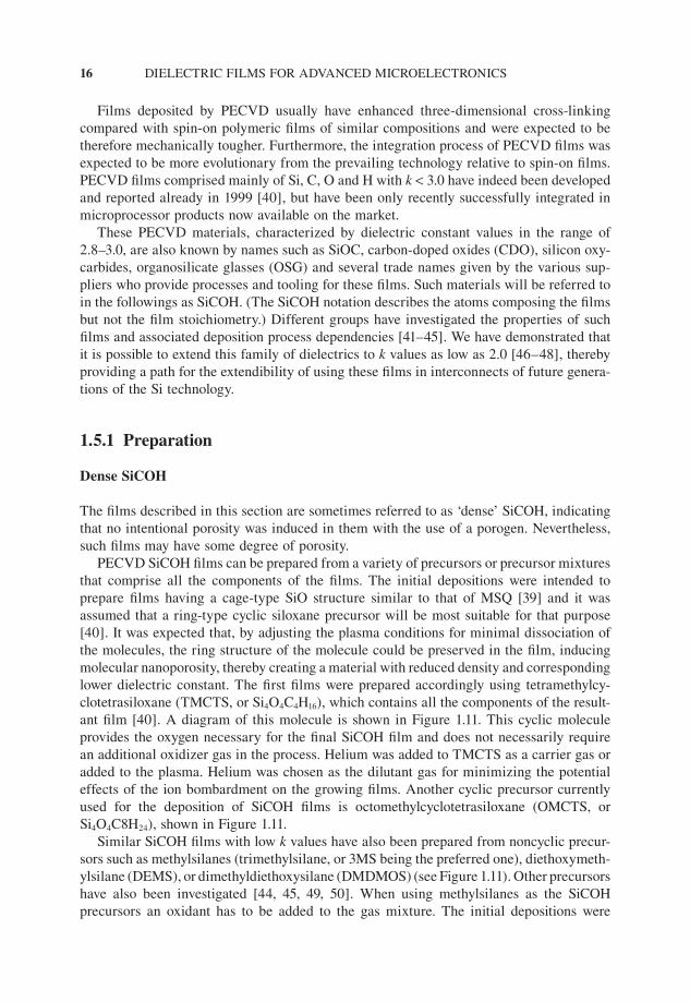
PECVD SiCOH fi lms can be prepared from a variety of precursors or precursor mixtures that comprise all the components of the fi lms. The initial depositions were intended to prepare fi lms having a cage-type SiO structure similar to that of MSQ [39] and it was assumed that a ring-type cyclic siloxane precursor will be most suitable for that purpose [40]. It was expected that, by adjusting the plasma conditions for minimal dissociation of the molecules, the ring structure of the molecule could be preserved in the fi lm, inducing molecular nanoporosity, thereby creating a material with reduced density and corresponding lower dielectric constant. The fi rst fi lms were prepared accordingly using tetramethylcy-clotetrasiloxane (TMCTS, or Si4O4C4H16), which contains all the components of the result-ant fi lm [40]. A diagram of this molecule is shown in Figure 1.11. This cyclic molecule provides the oxygen necessary for the fi nal SiCOH fi lm and does not necessarily require an additional oxidizer gas in the process. Helium was added to TMCTS as a carrier gas or added to the plasma. Helium was chosen as the dilutant gas for minimizing the potential effects of the ion bombardment on the growing fi lms. Another cyclic precursor currently used for the deposition of SiCOH fi lms is octomethylcyclotetrasiloxane (OMCTS, or Si4O4C8H24), shown in Figure 1.11.
Similar SiCOH fi lms with low k values have also been prepared from noncyclic precur-sors such as methylsilanes (trimethylsilane, or 3MS being the preferred one), diethoxymeth-ylsilane (DEMS), or dimethyldiethoxysilane (DMDMOS) (see Figure 1.11). Other precursors have also been investigated [44, 45, 49, 50]. When using methylsilanes as the SiCOH precursors an oxidant has to be added to the gas mixture. The initial depositions were
LOW AND ULTRALOW DIELECTRIC CONSTANT FILMS PREPARED 17
performed using N2O as the O source [51, 52], however it was found that this resulted in the incorporation of amine species in the fi lms. These amine species caused resist poisoning during lithography performed on such fi lms, therefore N2O was later replaced with O2 in the deposition process.
The deposition of SiCOH fi lms is typically performed in a parallel plate RF PECVD reactor. The power to sustain the plasma is provided by either one or two RF power supplies of different frequencies. A typical frequency for the main power supply is 13.56 MHz, while the second power supply is usually of lower frequency and it can be used to apply a negative DC bias to the substrate. The fi lms are deposited at temperatures up to about 400°C.
While SiCOH fi lms are still prepared from different precursors, it was found that superior fi lm properties are obtained when using cyclic precursors TMCTS [40] or OMCTS [18].
Porous SiCOH
One of the principal criteria for the choice of a new interconnect dielectric is its potential extendibility to later ULSI technology generations, requiring further reduced k values. The lowering of the dielectric constant of SiCOH below the values obtained for the dense fi lms can be achieved by introducing porosity in the SiCOH fi lms. It was claimed for many years that porosity can be introduced only in spin-on and not in PECVD fi lms, but we have demonstrated that this is not true. While porosity could be created to some extent by the PECVD process through the adjustment of the plasma conditions, it can be achieved and controlled much more effectively by a subtractive process (removal of a fraction of the deposited fi lm). The reduction of the dielectric constant can be accomplished by depositing multiphase fi lms containing at least one unstable CH phase in addition to the SiCOH
O
Si
O Si
O
Si
OSi
H
HH3C
CH3
CH3H
H
H3C
O
Si
O Si
O
Si
OSi
CH3
CH3H3C
CH3
CH3H3C
H3C
H3C
OMCTSTMCTS
CH3
CH3
CH3
H
Si
3MS
CH3CH2O
CH3CH2O
CH3
H
SiCH3O
CH3O
CH3
CH3
Si
DMDMOSDEMS
Figure 1.11 Schematic diagrams of some precursors used for the preparation of SiCOH fi lms

18 DIELECTRIC FILMS FOR ADVANCED MICROELECTRONICS
skeleton phase and treating the fi lms after deposition to remove the unstable phase from the material. (The CH notation refl ects the atomic compositions of the phase but not its stoichiometry.) Ultralow-k porous SiCOH (pSiCOH) fi lms can be prepared as a dual-phase SiCOH-CH material using the same PECVD method as described above and adding a hydrocarbon porogen (Por), as the CH precursor, to the SiCOH precursor feed to the reactor [46–48, 53].
During the deposition of pSiCOH the RF power needs to be adjusted and kept at levels small enough to prevent excessive dissociation of the SiCOH precursor, yet be suffi ciently high to dissociate the porogen and incorporate its CH fragments in the deposited fi lms. These requirements impose limitations on the choice of the organic precursor and on the plasma operating window for obtaining ultralow-k fi lms.
The removal of the porogen can be done by annealing the fi lms at 400–430°C in an inert ambient [46–48], or using e-beam or UV irradiation. The latter two techniques are much faster than the thermal anneal, can enhance the cross-linking in the cured fi lms and improve their mechanical properties [54, 55].
The results presented later for pSiCOH are for thermally annealed fi lms.
1.5.2 Properties of SiCOH and pSiCOH dielectrics
The structure of SiCOH and pSiCOH
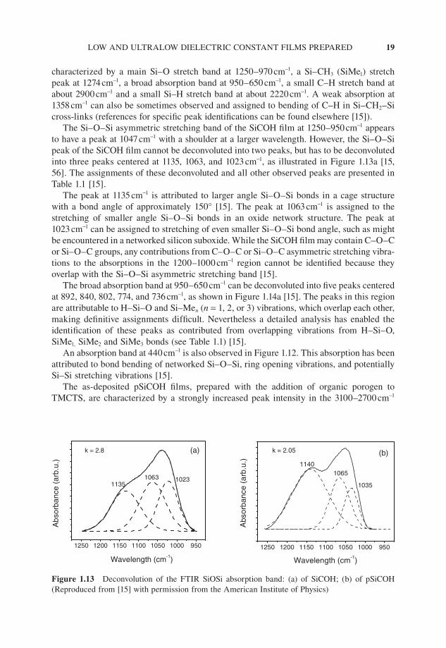
Structural characterization of amorphous fi lms is extremely diffi cult, but we have shown that it is possible to use FTIR to characterize the different bonding arrangements in the fi lms and to obtain insights in the structure of SiCOH [15]. Typical FTIR spectra of such fi lms are presented in Figure 1.12. The FTIR spectrum of a SiCOH fi lm (Figure 1.12a) is generally
3000 2500 2000 1500 1000 500
Abs
orba
nce
(arb
.u.)
Wavenumbers (cm-1)
(c)
(b)
(a)
Figure 1.12 FTIR spectra of SiCOH and pSiCOH fi lms: (a) SiCOH; (b) as-deposited pSiCOH; (c) annealed pSiCOH (Reproduced from [15] with permission from the American Institute of Physics)
LOW AND ULTRALOW DIELECTRIC CONSTANT FILMS PREPARED 19
characterized by a main Si–O stretch band at 1250–970 cm−1, a Si–CH3 (SiMe1) stretch peak at 1274 cm−1, a broad absorption band at 950–650 cm−1, a small C–H stretch band at about 2900 cm−1 and a small Si–H stretch band at about 2220 cm−1. A weak absorption at 1358 cm−1 can also be sometimes observed and assigned to bending of C–H in Si–CH2–Si cross-links (references for specifi c peak identifi cations can be found elsewhere [15]).
The Si–O–Si asymmetric stretching band of the SiCOH fi lm at 1250–950 cm−1 appears to have a peak at 1047 cm−1 with a shoulder at a larger wavelength. However, the Si–O–Si peak of the SiCOH fi lm cannot be deconvoluted into two peaks, but has to be deconvoluted into three peaks centered at 1135, 1063, and 1023 cm−1, as illustrated in Figure 1.13a [15, 56]. The assignments of these deconvoluted and all other observed peaks are presented in Table 1.1 [15].
The peak at 1135 cm−1 is attributed to larger angle Si–O–Si bonds in a cage structure with a bond angle of approximately 150° [15]. The peak at 1063 cm−1 is assigned to the stretching of smaller angle Si–O–Si bonds in an oxide network structure. The peak at 1023 cm−1 can be assigned to stretching of even smaller Si–O–Si bond angle, such as might be encountered in a networked silicon suboxide. While the SiCOH fi lm may contain C–O–C or Si–O–C groups, any contributions from C–O–C or Si–O–C asymmetric stretching vibra-tions to the absorptions in the 1200–1000 cm−1 region cannot be identifi ed because they overlap with the Si–O–Si asymmetric stretching band [15].
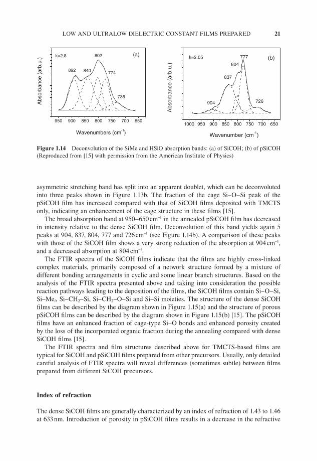
The broad absorption band at 950–650 cm−1 can be deconvoluted into fi ve peaks centered at 892, 840, 802, 774, and 736 cm−1, as shown in Figure 1.14a [15]. The peaks in this region are attributable to H–Si–O and Si–Men (n = 1, 2, or 3) vibrations, which overlap each other, making defi nitive assignments diffi cult. Nevertheless a detailed analysis has enabled the identifi cation of these peaks as contributed from overlapping vibrations from H–Si–O, SiMe1, SiMe2 and SiMe3 bonds (see Table 1.1) [15].
An absorption band at 440 cm−1 is also observed in Figure 1.12. This absorption has been attributed to bond bending of networked Si–O–Si, ring opening vibrations, and potentially Si–Si stretching vibrations [15].
The as-deposited pSiCOH fi lms, prepared with the addition of organic porogen to TMCTS, are characterized by a strongly increased peak intensity in the 3100–2700 cm−1
1250 1200 1150 1100 1050 1000 950
102310631135
(a)
Abs
orba
nce
(arb
.u.)
k = 2.8
Wavelength (cm-1)
1250 1200 1150 1100 1050 1000 950
1035
10651140
(b)
Wavelength (cm-1)
k = 2.05
Abs
orba
nce
(arb
.u.)
Figure 1.13 Deconvolution of the FTIR SiOSi absorption band: (a) of SiCOH; (b) of pSiCOH (Reproduced from [15] with permission from the American Institute of Physics)
20 DIELECTRIC FILMS FOR ADVANCED MICROELECTRONICS
region (C–Hi stretching vibrations), and reduced intensity of the 890 and 848 cm−1 absorp-tions (H–Si–O bending and SiMex vibrations), compared with the fi lms deposited from TMCTS only, as shown in Figure 1.12b. The new absorptions at 2932 (CH2 stretch) and 1461 cm−1 (CH2 bend, isolated from silicon) and the increased relative absorption of the CH2 stretch at 2875 cm−1 are the result of the incorporation of organic components in the as-deposited SiCOH fi lms.
The annealed pSiCOH fi lm has reduced C–Hi stretching band (3100–2700 cm−1) and CH2 bend peak (1461 cm−1) intensities (see Figure 1.12c) indicating a signifi cant loss of the CH from the dual phase fi lms during annealing. In the annealed pSiCOH fi lm, the Si–O–Si
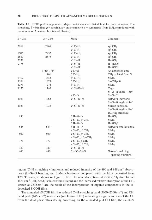
Table 1.1 FTIR peak assignments. Major contributors are listed fi rst for each vibration. n = stretching, d = bending, r = rocking, a = antisymmetric, s = symmetric (from [15], reproduced with permission of American Institute of Physics)
k = 2.8 k = 2.05 Mode Comment
2969 2968 n a C–H3 sp3 CH3
n s C–H3 sp3 CH3
2916 2932 n a C–H2 sp3 CH2
2880 2875 n s C–H2 sp3 CH2
2232 n s Si–H H–SiO3
2178 n s Si–H H–SiO2Si n s Si–H H–SiOSi 1740, 1714 n C=O As-deposited only 1461 d C–H2 CH2 isolated from Si 1412 1412 d a C–H3 SiMex
1358 1379 d C–H2 Si–CH2–Si 1273 1274 d s C–H3 SiMex
1135 1140 n a Si–O–Si Cage Si–O–Si angle ∼150° n C–O Si–O–C 1063 1065 n a Si–O–Si Network (network) Si–O–Si angle ∼144° 1023 1035 n a Si–O–Si Silicon suboxide, Si–O–Si angle <144° D3h ring structure 890 d H–Si–O H–SiO3
n Si–C, rs CH3 SiMe2
d H–Si–O H–SiO2Si 848 843 d H–Si–O Network smaller angle n Si–C, ra CH3 SiMe3
802 800 n Si–C, ra CH3 SiMe2
n Si–C, r Si–CH3 SiMe1
773 779 n Si–C, r CH3 SiMe1
n Si–C, rs CH3 SiMe3
730 720 n s Si–O–Si 440 440 d of O–Si–O Network and ring opening vibratins
LOW AND ULTRALOW DIELECTRIC CONSTANT FILMS PREPARED 21
asymmetric stretching band has split into an apparent doublet, which can be deconvoluted into three peaks shown in Figure 1.13b. The fraction of the cage Si–O–Si peak of the pSiCOH fi lm has increased compared with that of SiCOH fi lms deposited with TMCTS only, indicating an enhancement of the cage structure in these fi lms [15].
The broad absorption band at 950–650 cm−1 in the annealed pSiCOH fi lm has decreased in intensity relative to the dense SiCOH fi lm. Deconvolution of this band yields again 5 peaks at 904, 837, 804, 777 and 726 cm−1 (see Figure 1.14b). A comparison of these peaks with those of the SiCOH fi lm shows a very strong reduction of the absorption at 904 cm−1, and a decreased absorption at 804 cm−1.
The FTIR spectra of the SiCOH fi lms indicate that the fi lms are highly cross-linked complex materials, primarily composed of a network structure formed by a mixture of different bonding arrangements in cyclic and some linear branch structures. Based on the analysis of the FTIR spectra presented above and taking into consideration the possible reaction pathways leading to the deposition of the fi lms, the SiCOH fi lms contain Si–O–Si, Si–Mei, Si–CH2–Si, Si–CH2–O–Si and Si–Si moieties. The structure of the dense SiCOH fi lms can be described by the diagram shown in Figure 1.15(a) and the structure of porous pSiCOH fi lms can be described by the diagram shown in Figure 1.15(b) [15]. The pSiCOH fi lms have an enhanced fraction of cage-type Si–O bonds and enhanced porosity created by the loss of the incorporated organic fraction during the annealing compared with dense SiCOH fi lms [15].
The FTIR spectra and fi lm structures described above for TMCTS-based fi lms are typical for SiCOH and pSiCOH fi lms prepared from other precursors. Usually, only detailed careful analysis of FTIR spectra will reveal differences (sometimes subtle) between fi lms prepared from different SiCOH precursors.
Index of refraction
The dense SiCOH fi lms are generally characterized by an index of refraction of 1.43 to 1.46 at 633 nm. Introduction of porosity in pSiCOH fi lms results in a decrease in the refractive
950 900 850 800 750 700 650
(a)k=2.8
736
774
802
840892
Abs
orba
nce
(arb
.u.)
Wavenumbers (cm-1)
1000 950 900 850 800 750 700 650
(b)k=2.05
837
904
804
777
726
Abs
orba
nce
(arb
.u.)
Wavenumber (cm-1)
Figure 1.14 Deconvolution of the SiMe and HSiO absorption bands: (a) of SiCOH; (b) of pSiCOH (Reproduced from [15] with permission from the American Institute of Physics)

22 DIELECTRIC FILMS FOR ADVANCED MICROELECTRONICS
index of the fi lms due to the reduction in fi lm density. Figure 1.16 [56] illustrates the effect of increasing porogen content in the plasma on the index of refraction of annealed pSiCOH fi lms deposited from TMCTS and a specifi c porogen [56]. The index of refraction decreases to 1.33 with increasing Por/TMCTS ratio in the gas feed. As we shall see later, the Por/TMCTS ratio is directly correlated to the degree of porosity in the fi lms; therefore the decrease of the index of refraction shown in Figure 1.16 is caused by the increase in fi lm porosity.
The trend illustrated above for TMCTS-based fi lms is true for fi lms prepared from other SiCOH and porogen precursor combinations, however the values of the index of refractions of fi lms with same k values can be affected by the precursor mixture used for its preparation.
SiO
H
Si
CH3
OSi
CH3
H
Si O
CH3
CH3
CH3Si O
Si OSi
O SiHCH3
O
Si
O
Si
OSi
OSi
H OH
CH2
CH3
OSi
SiOHO
SiO
CH
CH3
HCH3
O
O
Si
CH2
O
OSi
O
H3C
H3C
Si CH3CH3
SiCH3
CH3
CH3O
Si OCH3
HSi O Si O Si H
CH3
CH3CH3CH3
H H
(a)
Si
O
Si O
Si
O
O Si
O
Si
O
Si O
Si
O
O Si CH3
H3C
O CH3
SiO
Si
O
H3C
O
O SiO
Si
H3C
O Si
CH3O
O
CH3
CH3
H3C
OSi
CH3
(b)
Figure 1.15 Diagram of the structure of (a) SiCOH; (b) pSiCOH fi lms (Reproduced from [15] with permission from the American Institute of Physics)
0.1 0.2 0.3 0.4 0.51.30
1.35
1.40
1.45
1.50
1.55
Por2/TMCTS flow rates
Inde
x of
ref
ract
ion
Figure 1.16 Index of refraction of pSiCOH fi lms vs porogen concentration in the plasma feed (Reproduced from [56] with permission from the American Institute of Physics)
LOW AND ULTRALOW DIELECTRIC CONSTANT FILMS PREPARED 23
Electrical properties
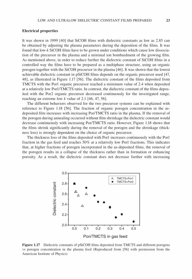
It was shown in 1999 [40] that SiCOH fi lms with dielectric constants as low as 2.85 can be obtained by adjusting the plasma parameters during the deposition of the fi lms. It was found that low-k SiCOH fi lms have to be grown under conditions which cause low dissocia-tion of the precursor in the plasma and a minimal ion bombardment of the growing fi lm. As mentioned above, in order to reduce further the dielectric constant of SiCOH fi lms in a controlled way the fi lms have to be prepared as a multiphase structure, using an organic porogen together with the SiCOH precursor in the plasma [46]. It was shown that the lowest achievable dielectric constant in pSiCOH fi lms depends on the organic precursor used [47, 48], as illustrated in Figure 1.17 [56]. The dielectric constant of the fi lms deposited from TMCTS with the Por1 organic precursor reached a minimum value of 2.4 when deposited at a relatively low Por1/TMCTS ratio. In contrast, the dielectric constant of the fi lms depos-ited with the Por2 organic precursor decreased continuously for the investigated range, reaching an extreme low k value of 2.1 [46, 47, 56].
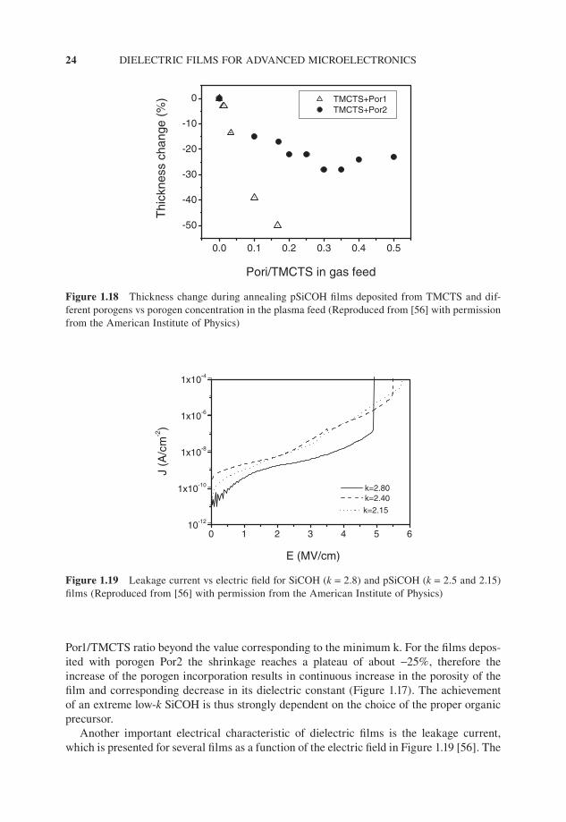
The different behaviors observed for the two precursor systems can be explained with reference to Figure 1.18 [56]. The fraction of organic porogen concentration in the as-deposited fi lm increases with increasing Por/TMCTS ratio in the plasma. If the removal of the porogen during annealing occurred without fi lm shrinkage the dielectric constant would decrease continuously with increasing Por/TMCTS ratio. However, Figure 1.18 shows that the fi lms shrink signifi cantly during the removal of the porogen and the shrinkage (thick-ness loss) is strongly dependent on the choice of organic precursor.
The thickness loss of the fi lms deposited with Por1 increases continuously with the Por1 fraction in the gas feed and reaches 50% at a relatively low Por1 fractions. This indicates that, at higher fractions of porogen incorporated in the as-deposited fi lms, the removal of the porogen results in a collapse of the thickness rather than in formation or enhancing porosity. As a result, the dielectric constant does not decrease further with increasing
0.0 0.1 0.2 0.3 0.4 0.52.0
2.2
2.4
2.6
2.8
3.0
Pori/TMCTS in gas feed
Die
lect
ric c
onst
ant
TMCTS+Por1 TMCTS+Por2
Figure 1.17 Dielectric constants of pSiCOH fi lms deposited from TMCTS and different porogens vs porogen concentration in the plasma feed (Reproduced from [56] with permission from the American Institute of Physics)
24 DIELECTRIC FILMS FOR ADVANCED MICROELECTRONICS
Por1/TMCTS ratio beyond the value corresponding to the minimum k. For the fi lms depos-ited with porogen Por2 the shrinkage reaches a plateau of about −25%, therefore the increase of the porogen incorporation results in continuous increase in the porosity of the fi lm and corresponding decrease in its dielectric constant (Figure 1.17). The achievement of an extreme low-k SiCOH is thus strongly dependent on the choice of the proper organic precursor.
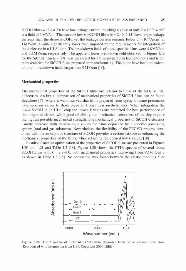
Another important electrical characteristic of dielectric fi lms is the leakage current, which is presented for several fi lms as a function of the electric fi eld in Figure 1.19 [56]. The
0.0 0.1 0.2 0.3 0.4 0.5
-50
-40
-30
-20
-10
0
Pori/TMCTS in gas feed
TMCTS+Por1 TMCTS+Por2
Thi
ckne
ss c
hang
e (%
)
Figure 1.18 Thickness change during annealing pSiCOH fi lms deposited from TMCTS and dif-ferent porogens vs porogen concentration in the plasma feed (Reproduced from [56] with permission from the American Institute of Physics)
0 1 2 3 4 5 610-12
1x10⁻¹⁰
1x10⁻⁸
1x10⁻⁶
1x10⁻⁴
J (A
/cm
-2)
E (MV/cm)
k=2.15
k=2.80 k=2.40
Figure 1.19 Leakage current vs electric fi eld for SiCOH (k = 2.8) and pSiCOH (k = 2.5 and 2.15) fi lms (Reproduced from [56] with permission from the American Institute of Physics)
LOW AND ULTRALOW DIELECTRIC CONSTANT FILMS PREPARED 25
SiCOH fi lms with k = 2.8 have low leakage current, reaching a value of only 2 × 10⁻¹⁰ A/cm2 at a fi eld of 1 MV/cm. The extreme low-k pSiCOH fi lms (k = 2.40, 2.15) have larger leakage currents than the dense SiCOH, yet the leakage current remains below 2 × 10⁻⁹ A/cm2 at 1 MV/cm, a value signifi cantly lower than imposed by the requirements for integration of the dielectric in a ULSI chip. The breakdown fi elds of these specifi c fi lms were 4.8 MV/cm and 5.5 MV/cm, respectively. The apparent lower breakdown fi eld observed in Figure 1.19 for the SiCOH fi lm (k = 2.8) was measured for a fi lm prepared in lab conditions and is not representative for SiCOH fi lms prepared in manufacturing. The latter have been optimized to obtain breakdown fi elds larger than 9 MV/cm [18].
Mechanical properties
The mechanical properties of the SiCOH fi lms are inferior to those of the SiO2 or FSG dielectrics. An initial comparison of mechanical properties of SiCOH fi lms can be found elsewhere [57] where it was observed that fi lms prepared from cyclic siloxane precursors have superior values to those prepared from linear methylsilanes. When integrating the low-k SiCOH in an ULSI chip the lowest k values are preferred for best performance of the integrated circuit, while good reliability and mechanical robustness of the chip require the highest possible mechanical strength. The mechanical properties of SiCOH dielectrics usually decrease with decreasing k values for fi lms deposited by a specifi c processing system (tool and gas mixtures). Nevertheless, the fl exibility of the PECVD process com-bined with the amorphous structure of SiCOH provides a certain latitude in enhancing the mechanical properties of the fi lms, while retaining the desired low k values [18].
Results of such an optimization of the properties of SiCOH fi lms are presented in Figures 1.20 and 1.21 and Table 1.2 [18]. Figure 1.20 shows the FTIR spectra of several dense SiCOH fi lms with k = 2.8–3.0, with mechanical properties improving from V2 to Gen 3 as shown in Table 1.2 [18]. No correlation was found between the elastic modulus E or
3000 2000 1000
Gen 3
Gen 2
Gen 1
V2
Abs
orba
nce
(arb
.u.)
Wavenumber (cm-1)
Figure 1.20 FTIR spectra of different SiCOH fi lms deposited from cyclic siloxane precursors (Reproduced with permission from [18], Copyright 2004 IEEE)
26 DIELECTRIC FILMS FOR ADVANCED MICROELECTRONICS
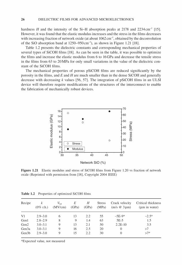
hardness H and the intensity of the Si–H absorption peaks at 2178 and 2234 cm−1 [15]. However, it was found that the elastic modulus increases and the stress in the fi lms decreases with increasing fraction of network oxide (at about 1062 cm−1, obtained by the deconvolution of the SiO absorption band at 1250–950 cm−1), as shown in Figure 1.21 [18].
Table 1.2 presents the dielectric constants and corresponding mechanical properties of several types of SiCOH fi lms [18]. As can be seen in the table, it was possible to optimize the fi lms and increase the elastic modulus from 6 to 16 GPa and decrease the tensile stress in the fi lms from 63 to 20 MPa for only small variations in the value of the dielectric con-stant of the SiCOH fi lms.
The mechanical properties of porous pSiCOH fi lms are reduced signifi cantly by the porosity in the fi lms, and E and H are much smaller than in the dense SiCOH and generally decrease with decreasing k values [56, 57]. The integration of pSiCOH fi lms in an ULSI device will therefore require modifi cations of the structures of the interconnect to enable the fabrication of mechanically robust devices.
0
2
4
6
8
10
12
14
16
30 35 40 45 500
10
20
30
40
50
60
70
Ela
stic
mod
ulus
(G
Pa)
Modulus
Str
ess
(MP
a)
Network SiO (%)
Stress
Figure 1.21 Elastic modulus and stress of SiCOH fi lms from Figure 1.20 vs fraction of network oxide (Reprinted with permission from [18], Copyright 2004 IEEE)
Table 1.2 Properties of optimized SiCOH fi lms
Recipe k Vbd E H Stress Crack velocity Critical thickness (0% r.h.) (MV/cm) (GPa) (GPa) (MPa) (m/s @ 3 µm) (µm in water)
V1 2.9–3.0 6 13 2.2 55 ∼5E-9* ∼2.5*Gen1 2.8–2.9 8 9 1.4 63 5E-5 1.5Gen2 3.0–3.1 9 13 2.1 50 2.2E-10 3.5Gen3a 3.0–3.1 9 16 2.5 20 0 >7Gen3b 2.9–3.0 9 15 2.2 30 0 >7*
*Expected value, not measured
LOW AND ULTRALOW DIELECTRIC CONSTANT FILMS PREPARED 27
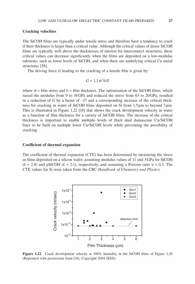
Cracking velocities
The SiCOH fi lms are typically under tensile stress and therefore have a tendency to crack if their thickness is larger than a critical value. Although the critical values of dense SiCOH fi lms are typically well above the thicknesses of interest for interconnect structures, these critical values can decrease signifi cantly when the fi lms are deposited on a low-modulus substrate, such as lower levels of SiCOH, and when there are underlying critical Cu metal structures [58].
The driving force G leading to the cracking of a tensile fi lm is given by:
G = 1.1 s 2h/E
where s = fi lm stress and h = fi lm thickness. The optimization of the SiCOH fi lms, which raised the modulus from 9 to 16 GPa and reduced the stress from 63 to 20 GPa, resulted in a reduction of G by a factor of ∼17 and a corresponding increase of the critical thick-ness for cracking in water of SiCOH fi lms deposited on Si from 1.5 µm to beyond 7 µm. This is illustrated in Figure 1.22 [18] that shows the crack development velocity in water as a function of fi lm thickness for a variety of SiCOH fi lms. The increase of the critical thickness is important to enable multiple levels of thick dual damascene Cu/SiCOH lines to be built on multiple lower Cu/SiCOH levels while preventing the possibility of cracking.
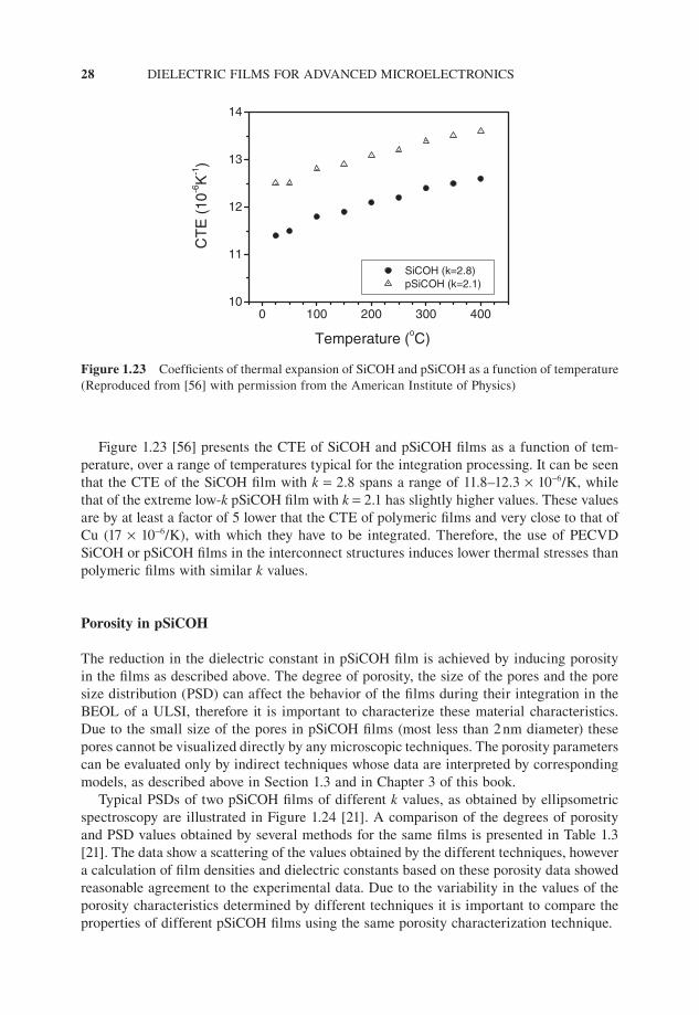
Coeffi cient of thermal expansion
The coeffi cient of thermal expansion (CTE) has been determined by measuring the stress in fi lms deposited on a silicon wafer, assuming modulus values of 11 and 3 GPa for SiCOH (k = 2.8) and pSiCOH (k = 2.1), respectively, and assuming a Poisson ratio n = 0.3. The CTE values for Si were taken from the CRC Handbook of Chemistry and Physics.
1 2 3 4 5 610-12
1x10⁻¹⁰
1x10⁻⁸
1x10⁻⁶
1x10⁻⁴
detection limit
Cra
ck v
eloc
ity (
m/s
ec)
Film Thickness (µm)
Gen1 Gen2 Gen3
Figure 1.22 Crack development velocity at 100% humidity in the SiCOH fi lms of Figure 1.20 (Reprinted with permission from [18], Copyright 2004 IEEE)
28 DIELECTRIC FILMS FOR ADVANCED MICROELECTRONICS
Figure 1.23 [56] presents the CTE of SiCOH and pSiCOH fi lms as a function of tem-perature, over a range of temperatures typical for the integration processing. It can be seen that the CTE of the SiCOH fi lm with k = 2.8 spans a range of 11.8–12.3 × 10⁻⁶/K, while that of the extreme low-k pSiCOH fi lm with k = 2.1 has slightly higher values. These values are by at least a factor of 5 lower that the CTE of polymeric fi lms and very close to that of Cu (17 × 10−6/K), with which they have to be integrated. Therefore, the use of PECVD SiCOH or pSiCOH fi lms in the interconnect structures induces lower thermal stresses than polymeric fi lms with similar k values.
Porosity in pSiCOH
The reduction in the dielectric constant in pSiCOH fi lm is achieved by inducing porosity in the fi lms as described above. The degree of porosity, the size of the pores and the pore size distribution (PSD) can affect the behavior of the fi lms during their integration in the BEOL of a ULSI, therefore it is important to characterize these material characteristics. Due to the small size of the pores in pSiCOH fi lms (most less than 2 nm diameter) these pores cannot be visualized directly by any microscopic techniques. The porosity parameters can be evaluated only by indirect techniques whose data are interpreted by corresponding models, as described above in Section 1.3 and in Chapter 3 of this book.
Typical PSDs of two pSiCOH fi lms of different k values, as obtained by ellipsometric spectroscopy are illustrated in Figure 1.24 [21]. A comparison of the degrees of porosity and PSD values obtained by several methods for the same fi lms is presented in Table 1.3 [21]. The data show a scattering of the values obtained by the different techniques, however a calculation of fi lm densities and dielectric constants based on these porosity data showed reasonable agreement to the experimental data. Due to the variability in the values of the porosity characteristics determined by different techniques it is important to compare the properties of different pSiCOH fi lms using the same porosity characterization technique.
0 100 200 300 40010
11
12
13
14
Temperature (oC)
CT
E (
10-6K
-1)
SiCOH (k=2.8) pSiCOH (k=2.1)
Figure 1.23 Coeffi cients of thermal expansion of SiCOH and pSiCOH as a function of temperature (Reproduced from [56] with permission from the American Institute of Physics)

LOW AND ULTRALOW DIELECTRIC CONSTANT FILMS PREPARED 29
1.5.3 Integration of SiCOH as the interconnect dielectric
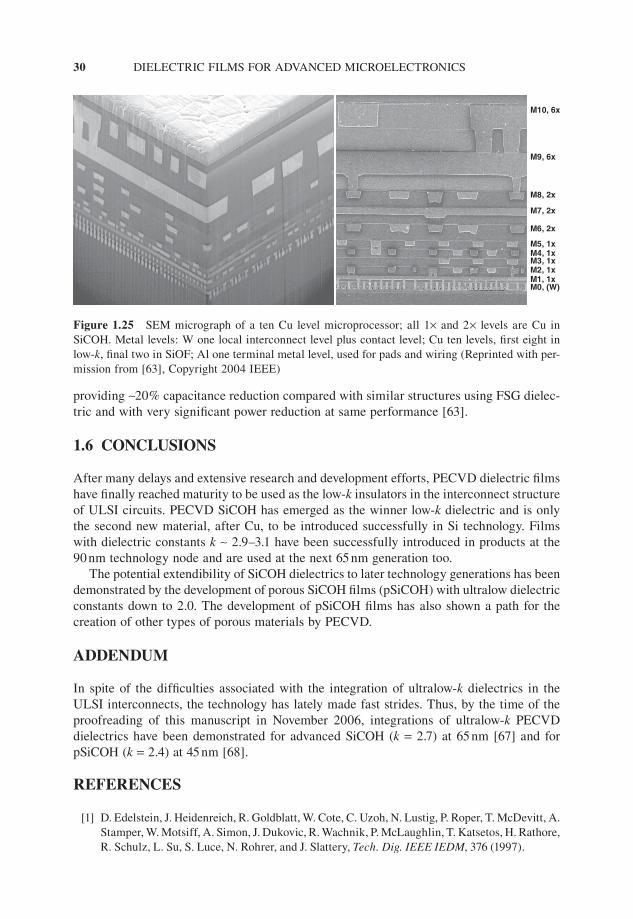
The initial integration of PECVD low-k SiCOH fi lms with Cu metallization for 130 and 90 nm CMOS has been reported by a number of institutions as early as 2000 [59–62], however its incorporation in semiconductor products has been achieved only in the 90 nm technology. Recent presentations on Cu/SiCOH interconnect integration show that the integration of SiCOH with the Cu metallization has become the predominant path chosen by the industry for the interconnect structures at the 90 nm technology [63–66]. At IBM, the optimization of the SiCOH characteristics has enabled the successful Cu/SiCOH inte-gration with a full-generation capacitance reduction relative to Cu/FSG with no reduction in reliability levels [63].
Figure 1.25 [63] shows a cross-section of an IBM interconnect structure in 90 nm Cu/low-k technology consisting of ten levels of Cu wiring plus one W local interconnect and one Al(Cu) terminal level. The Cu wiring has four hierarchical scaling factors for pitches and cross-sectional dimensions, denoted as 1×, 2×, and 6×. All 1× and 2× levels are built with low-k SiCOH dielectric, and the fi nal two 6× levels are built with SiOF (FSG). Such a structure has already been incorporated in IBM’s products based on the 90 nm technology
12
10
8
6
4
2
00.1 1 10 100
Pore Radius (nm)
(1/V
)*dV
/dR
max
AdsorptionDesorption
(a)10
0.1 1 10 100Pore Radius (nm)
AdsorptionDesorption8
6
4
2
0
(1/V
)*dV
/dR
max
(b)
Figure 1.24 Pore size distribution in pSiCOH fi lms: (a) k = 2.40; (b) k = 2.05 (Reproduced from [21] with permission from the American Institute of Physics)
Table 1.3 Porosity and average pore size in SiCOH and pSiCOH fi lms (Reproduced from [21] with permission from American Institute of Physics)
Sample k Degree of porosity (%) Pore diameter (nm)
PAS XR EP PALS SAXS EP
SiCOH 2.85 0 0 0 N/A N/A N/ApSiCOH 2.40 20 13 17 1–4 <1.6 1.3pSiCOH 2.05 29 22 28 1–7 <2.2 <5
30 DIELECTRIC FILMS FOR ADVANCED MICROELECTRONICS
providing ∼20% capacitance reduction compared with similar structures using FSG dielec-tric and with very signifi cant power reduction at same performance [63].
1.6 CONCLUSIONS
After many delays and extensive research and development efforts, PECVD dielectric fi lms have fi nally reached maturity to be used as the low-k insulators in the interconnect structure of ULSI circuits. PECVD SiCOH has emerged as the winner low-k dielectric and is only the second new material, after Cu, to be introduced successfully in Si technology. Films with dielectric constants k ∼ 2.9–3.1 have been successfully introduced in products at the 90 nm technology node and are used at the next 65 nm generation too.
The potential extendibility of SiCOH dielectrics to later technology generations has been demonstrated by the development of porous SiCOH fi lms (pSiCOH) with ultralow dielectric constants down to 2.0. The development of pSiCOH fi lms has also shown a path for the creation of other types of porous materials by PECVD.
ADDENDUM
In spite of the diffi culties associated with the integration of ultralow-k dielectrics in the ULSI interconnects, the technology has lately made fast strides. Thus, by the time of the proofreading of this manuscript in November 2006, integrations of ultralow-k PECVD dielectrics have been demonstrated for advanced SiCOH (k = 2.7) at 65 nm [67] and for pSiCOH (k = 2.4) at 45 nm [68].
REFERENCES
[1] D. Edelstein, J. Heidenreich, R. Goldblatt, W. Cote, C. Uzoh, N. Lustig, P. Roper, T. McDevitt, A. Stamper, W. Motsiff, A. Simon, J. Dukovic, R. Wachnik, P. McLaughlin, T. Katsetos, H. Rathore, R. Schulz, L. Su, S. Luce, N. Rohrer, and J. Slattery, Tech. Dig. IEEE IEDM, 376 (1997).
M1, 1xM2, 1xM3, 1xM4, 1xM5, 1x
M6, 2x
M9, 6x
M7, 2x
M8, 2x
M10, 6x
M0, (W)
Figure 1.25 SEM micrograph of a ten Cu level microprocessor; all 1× and 2× levels are Cu in SiCOH. Metal levels: W one local interconnect level plus contact level; Cu ten levels, fi rst eight in low-k, fi nal two in SiOF; Al one terminal metal level, used for pads and wiring (Reprinted with per-mission from [63], Copyright 2004 IEEE)
LOW AND ULTRALOW DIELECTRIC CONSTANT FILMS PREPARED 31
[2] S. Venkatesan et al. Tech. Dig. IEEE IEDM, 769 (1997). [3] International Technology Roadmap for Semiconductors, 2003 Edition, International
SEMATECH, 2706 Montopolis Drive Austin, TX 78741, USA. [4] The National Technology Roadmap for Semiconductors, San Jose, SIA, 1997. [5] C. Case, Solid State Technol., 26, January (2005). [6] Mat. Res. Soc. Symp. Proc., 381 (1995), 443 (1996), 476 (1997), 511 (1998). [7] The Electrochemical Soc. Proc. Series, PV97-8 (1997), PV98-3 (1998), PV99-7 (1999). [8] M. McCoy, 2000 C&EN, 17, (2000). [9] L. Peters, Semiconductor International, 23(6), 108 (2000). [10] A. Grill, Cold Plasma in Materials Fabrication: From Fundamentals to Applications, Wiley-
IEEE Press, Hoboken, NJ, 2001. [11] A. Grill, V. Patel, and C. Jahnes, J. Electrochemical Soc., 145, 1649 (1998). [12] A. Grill, C. Jahnes, J. Ott, V. Patel, and S. Cohen, J. Hummel, R. Mih, and J. Liu, Electrochemi-
cal Society Proceedings, PV 98-3, 118 (1998). [13] Computer Graphics Services, CGS, Ithaca, NY. [14] n&k Analyzer 1280 from n&k Technology, Inc. 4051 Burton Drive, Santa Clara, California, 95054. [15] A. Grill and D.A. Neumayer, J. Appl. Phys., 94, 6697 (2003). [16] A. Grill, V. Patel, and S. Cohen, Diamond and Related Materials, 3, 281 (1994). [17] A. Grill and B.S. Meyerson, Ch.5 in Synthetic Diamond: Emerging CVD Science and Technol-
ogy, K.E. Spear and J.P. Dismukes (eds), John Wiley & Sons, Inc., New York, 1994. [18] A. Grill, D. Edelstein, D. Restaino, M. Lane, S. Gates, E. Liniger, T. Shaw, X-H. Liu, D. Klaus,
V. Patel, S. Cohen, E. Simonyi, N. Klymko, S. Lane, K. Ida, S. Vogt T. Van Kleeck, C. Davis, M. Ono, T. Nogami, and T. Ivers, Proc. IEEE 2004 Internat. Interconnect Technol. Conference, IEEE, Piscataway, NJ (IEEE Catalog No. 04TH8729) 54 (2004).
[19] R.F. Cook and E.G. Liniger, Mat. Res. Soc. Symp. Proc., 511, 171 (1998). [20] C. Donnet, J. Fontaine, A. Grill, V. Patel, C. Jahnes, and M. Belin, Surf. Coat. Technol., 94–95,
531 (1997). [21] A. Grill, V. Patel, K.P. Rodbell, and E. Huang, M.R. Baklanov and K.P. Mogilnikov, M. Toney,
and H.-C. Kim, J. Appl. Phys., 94, 3427 (2003). [22] Hae-Jeong Lee, Christopher L. Soles, Da-Wei Liu, Barry J. Bauer, Eric K. Lin, Wen-li Wu, and
Alfred Grill, J. Appl. Phys., 95, 2355 (2004). [23] C.L. Soles, H.-J. Lee, E.K. Lin, and W.-L. Wu., Special Publication 960–13, NIST, U.S. Gov-
ernment Printing Offi ce, Washington, DC, 2004. [24] A. Grill, Diamond and Related Materials, 8, 428 (1999). [25] A. Grill, V. Patel, S.A. Cohen, D.C. Edelstein, J.R. Paraszczak, and C. Jahnes, Proc. Advanced
Metallization and Interconnect Systems for ULSI Applications in 1996, October 1–3, Boston, R. Haveman, J. Schmitz, H. Komiyama and K. Tsubouchi (eds), Materials Research Society, Pittsburg, PA, 417, (1997).
[26] A. Grill, V. Patel, K.L. Saenger, C. Jahnes, S.A. Cohen, A.G. Schrott, D.C. Edelstein, and J.R. Paraszczak, Mat. Res. Soc. Symp. Proc., 443, 155 (1997).
[27] S. Takeishi, H. Kudo, R. Shinohara, M. Hashino, S. Fukuyama, J. Yamaguchi, and M. Yamada, J. Electrochem. Soc., 144, 1797 (1997).
[28] Y. Matsubara, K. Endo, T. Tatsumi, H. Ueno, K. Sugai, and T. Horiuchi, IEDM, 96, 369 (1996). [29] Y. Matsubara, K. Endo, M. Iguchi, N. Ito, K. Aoyama, T. Tatsumi, and T. Horiuchi, Mat. Res.
Soc. Symp. Proc., 511, 291 (1998). [30] H. Kudo, R. Shinohara, and Y. Yamada, Mat. Res. Soc. Proc., 381, 105, (1995). [31] K. Endo and T. Tatsumi, Mat. Res. Soc. Proc., 381, 135, (1995). [32] J.P. Sulivan, T.A. Friedmann, C.A. Apblett, M.P. Siegal, N. Missert, M.L. Lovejoy, P.B.
Mirkarimi, and K.F. McCarty, Mat. Res. Soc. Proc. 381, 273, (1995). [33] A. Grill, Diamond and Related Materials, 10(2), 234 (2001). [34] A. Grill, C. Jahnes, V. Patel, J. Ott, J. Hummel, R. Mih, and J. Liu, Mat. Res. Soc. Symp. Proc.,
511, 223 (1998).
32 DIELECTRIC FILMS FOR ADVANCED MICROELECTRONICS
[35] H. Yang, T. Nguyen, Y. Ma, and S.-T. Hsu, 1998 DUMIC Conference, 38 (1998). [36] A. Grill, J.P. Hummel, C.V. Jahnes, V.V. Patel, and K.L. Saenger, US Patent 6140226, Issued
10/31/2000. [37] E.T. Ryan, A.J. McKerrow, J. Leu, and P.S. Ho, MRS Bulletin 22, 49 (1997). [38] N.P. Hacker, G. Davis, L. Figge, T. Krajewski, S. Lefferts, J. Nedbal, and R. Spear, Mat. Res.
Soc. Symp. Proc., 476, 25 (1997). [39] M.J. Loboda, C.M. Grove, and R.F. Schneider, J. Electrochem. Soc. 145, 2861 (1998). [40] A. Grill, L. Perraud, V. Patel, C. Jahnes, and S. Cohen, Mat. Res. Soc. Symp. Proc., 565, 107
(1999). [41] Y.Y. Cheng, L.C. Chao, S.M. Jang, C.H. Yu, and M.S. Liang, Proc. IEEE 2000 Internat. Inter-
connect Technol. Conf., 161 (2000). [42] M. Loboda, J. Seifferly, C. Grove, and R. Schneider, Mat. Res. Soc. Proc. 447, 145 (1997). [43] R.A. Donaton, et al., Mat. Res. Soc. Proc., 612, D5.14.1 (2000). [44] H. Ikakura, et al., Conf. Proc. ULSI VXI, 611 (2001) (MRS, Warrendale, PA). [45] M. Tada, J. Kawahara, and Y. Hayashi, Conf. Proc. ULSI VXI, 579 (2001) (MRS, Warrendale,
PA). [46] A. Grill and V. Patel, Electrochemical Soc. Proc., 2000–5, 55 (2000). [47] A. Grill and V. Patel, Mat. Res. Soc. Symp. Proc., 612, D291 (2001). [48] A. Grill and V. Patel, Appl. Phys. Lett., 79(6), 803 (2001). [49] M. O’Neil, A. Lukas, R. Vrtis, J. Vincent, B. Peterson, M. Bitner, and E. Karwacki, Semicon-
ductor International, 26(6), 93 (2002). [50] Q. Wu and K.K. Gleason, Plasma and Polymers, 8, 31 (2003). [51] Newsbytes PM, November 6 (1998) [52] B.K. Hwang, M.J. Loboda, G.A. Cerny, R.F. Schneider, and J.A. Seifferly, Electrochemical
Soc. Proc., PV2000–5, 63 (2000). [53] R. Vrtis, M.L. O’Neil, J.L. Vincent, A.S. Lucas, B.K. Peterson, M.D. Bitner, E.J. Karwacki,
Mat. Res. Symp. Proc., 766, 259 (2003). [54] K. Fujita, H. Miyajima, R. Nakata, and N. Miyashita, Proceedings of the IEEE 2003 Intern.
Interconnect Technol. Conference, (IEEE, Piscataway, NJ) paper 6.4 (2003). [55] C. Waldfried, Advanced Dielectric Materials Seminar, organized by Axcelis, Oct. 17, 2004,
San-Diego, CA. [56] A. Grill, J. Appl. Phys., 93, 1785 (2003). [57] A. Grill, D. Edelstein, and V. Patel, Conf. Proc. ULSI, XVII, 253 (2002), (MRS, Warrendale, PA). [58] J.M. Ambrico, E.E. Jones, and M.R. Begley, Int. J. Solids and Structures, 39, 1443 (2002). [59] S. Thompson, et al., 2002 IEDM Technical Digest, 61 (2002) (IEEE Catalog nr. 02CH37358,
Piscataway, NJ). [60] M. Matsuura et al., Conf. Proc. ULSI, VXIII, 493 (2003) MRS, Warrendale, PA. [61] R.A. Donaton et al., Conf. Proc. ULSI, VXI, 595 (2001) MRS, Warrendale, PA. [62] P. Wrshka, G. Lee, K.-S. Low, K. Dev, D. Dobuzinsky, R. Conti, and P. Schafer, Conf. Proc.
ULSI, VXI, 549 (2001) MRS, Warrendale, PA. [63] D. Edelstein et al., Proceedings of the IEEE 2004 Intern. Interconnect Technol. Conf., IEEE,
Piscataway, NJ (IEEE Catalog No. 04TH8729), 214 (2004). [64] H. Ruelke, P. Huebler, C. Streck, M. Gotuaco, and W. Senninger, Solid State Technol., 47(1),
60 (2004). [65] C.-H. Jan et al., Proceedings of the IEEE 2004 Intern. Interconnect Technol. Conf, IEEE,
Piscataway, NJ (IEEE Catalog No. 04TH8729), 205 (2004). [66] C.C. Jeng et al., Proceedings of the IEEE 2004 Intern. Interconnect Technol. Conf.,
IEEE, Piscataway, NJ (IEEE Catalog No. 04TH8729), 199 (2004).[67] V. McGahay et al., Proceedings of the IEEE 2006 Intern. Interconnect Technol. Conf., IEEE,
Piscataway, NJ, (IEEE Catalog Number: 06TH8862C) paper 9.[68] S. Sankaran et al., Presented at IEDM 2006.
![5th lecture [ Interference in dielectric films., Newton ring Exp.] 1....5th lecture [ Interference in dielectric films., Newton ring Exp.] 1. Interference in Dielectric films The familiar](https://img.dokumen.tips/doc/110x75/609e4ced5557b45107506b96/5th-lecture-interference-in-dielectric-films-newton-ring-exp-1-5th-lecture.jpg)