Embed Size (px)
Citation preview
December 2014 DocID026975 Rev 1 1/49
49
UM1823User manual
1 kW three-phase motor control evaluation board featuring L6390drivers and STGP10H60DF IGBT
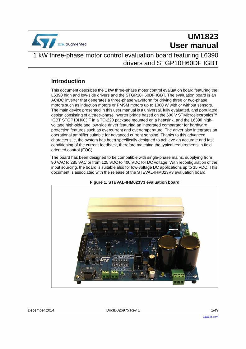
IntroductionThis document describes the 1 kW three-phase motor control evaluation board featuring the L6390 high and low-side drivers and the STGP10H60DF IGBT. The evaluation board is an AC/DC inverter that generates a three-phase waveform for driving three or two-phase motors such as induction motors or PMSM motors up to 1000 W with or without sensors. The main device presented in this user manual is a universal, fully evaluated, and populated design consisting of a three-phase inverter bridge based on the 600 V STMicroelectronics™ IGBT STGP10H60DF in a TO-220 package mounted on a heatsink, and the L6390 high-voltage high-side and low-side driver featuring an integrated comparator for hardware protection features such as overcurrent and overtemperature. The driver also integrates an operational amplifier suitable for advanced current sensing. Thanks to this advanced characteristic, the system has been specifically designed to achieve an accurate and fast conditioning of the current feedback, therefore matching the typical requirements in field oriented control (FOC).
The board has been designed to be compatible with single-phase mains, supplying from 90 VAC to 285 VAC or from 125 VDC to 400 VDC for DC voltage. With reconfiguration of the input sourcing, the board is suitable also for low-voltage DC applications up to 35 VDC. This document is associated with the release of the STEVAL-IHM023V3 evaluation board.
Figure 1. STEVAL-IHM023V3 evaluation board
www.st.com
Contents UM1823
2/49 DocID026975 Rev 1
Contents
1 System introduction . . . . . . . . . . . . . . . . . . . . . . . . . . . . . . . . . . . . . . . . . 6
1.1 Main characteristics . . . . . . . . . . . . . . . . . . . . . . . . . . . . . . . . . . . . . . . . . . 6
1.2 Target applications . . . . . . . . . . . . . . . . . . . . . . . . . . . . . . . . . . . . . . . . . . . 6
1.3 Safety and operating instructions . . . . . . . . . . . . . . . . . . . . . . . . . . . . . . . . 7
1.3.1 General terms . . . . . . . . . . . . . . . . . . . . . . . . . . . . . . . . . . . . . . . . . . . . . 7
1.3.2 evaluation board intended use . . . . . . . . . . . . . . . . . . . . . . . . . . . . . . . . . 7
1.3.3 evaluation board installation . . . . . . . . . . . . . . . . . . . . . . . . . . . . . . . . . . 7
1.3.4 Electrical connections . . . . . . . . . . . . . . . . . . . . . . . . . . . . . . . . . . . . . . . 8
1.3.5 evaluation board operation . . . . . . . . . . . . . . . . . . . . . . . . . . . . . . . . . . . 8
2 Board description . . . . . . . . . . . . . . . . . . . . . . . . . . . . . . . . . . . . . . . . . . . 9
2.1 System architecture . . . . . . . . . . . . . . . . . . . . . . . . . . . . . . . . . . . . . . . . . . 9
2.2 The board schematic . . . . . . . . . . . . . . . . . . . . . . . . . . . . . . . . . . . . . . . . 10
2.3 Circuit description . . . . . . . . . . . . . . . . . . . . . . . . . . . . . . . . . . . . . . . . . . . 16
2.3.1 Power supply . . . . . . . . . . . . . . . . . . . . . . . . . . . . . . . . . . . . . . . . . . . . . 16
2.3.2 Inrush limitation . . . . . . . . . . . . . . . . . . . . . . . . . . . . . . . . . . . . . . . . . . . 17
2.3.3 Brake function . . . . . . . . . . . . . . . . . . . . . . . . . . . . . . . . . . . . . . . . . . . . 17
2.3.4 Gate driving circuit . . . . . . . . . . . . . . . . . . . . . . . . . . . . . . . . . . . . . . . . . 18
2.3.5 Overcurrent protection . . . . . . . . . . . . . . . . . . . . . . . . . . . . . . . . . . . . . . 18
2.3.6 Current sensing amplifying network . . . . . . . . . . . . . . . . . . . . . . . . . . . . 19
2.3.7 The tachometer and Hall/encoder inputs . . . . . . . . . . . . . . . . . . . . . . . . 23
2.3.8 Temperature feedback and overtemperature protection . . . . . . . . . . . . 23
3 Hardware setting of the STEVAL-IHM023V3 . . . . . . . . . . . . . . . . . . . . . 24
3.1 Hardware settings for six-step (block commutation) control of BLDC motors . . . . . . . . . . . . . . . . . . . . . . . . . . . . . . . . . . . . . . . . . . . . . . 24
3.2 Hardware settings for “Field Oriented Control” (FOC) in single-shunt topology current reading configuration . . . . . . . . . . . . . . . . . . . . . . . . . . . 26
3.3 Hardware settings for FOC in three-shunt configuration . . . . . . . . . . . . . 27
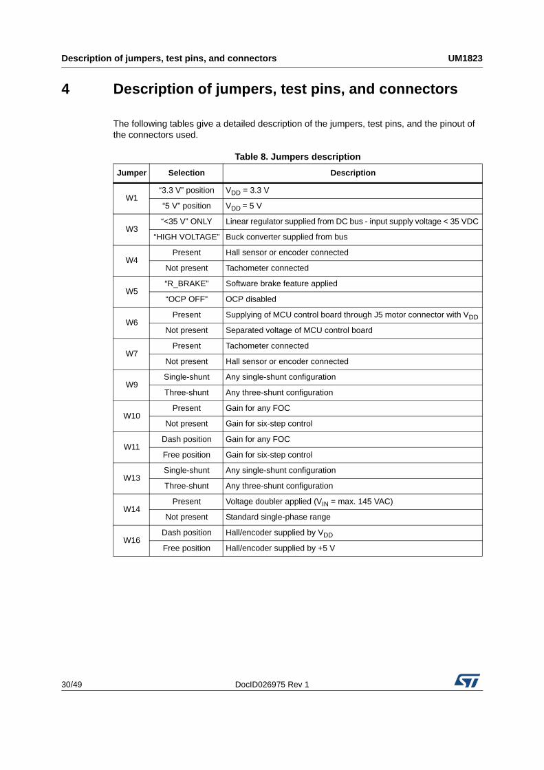
4 Description of jumpers, test pins, and connectors . . . . . . . . . . . . . . . 30
5 Connector placement . . . . . . . . . . . . . . . . . . . . . . . . . . . . . . . . . . . . . . . 33
DocID026975 Rev 1 3/49
UM1823 Contents
49
6 Bill of material . . . . . . . . . . . . . . . . . . . . . . . . . . . . . . . . . . . . . . . . . . . . . 34
7 PCB layout . . . . . . . . . . . . . . . . . . . . . . . . . . . . . . . . . . . . . . . . . . . . . . . . 40
8 Ordering information . . . . . . . . . . . . . . . . . . . . . . . . . . . . . . . . . . . . . . . 44
9 Using STEVAL-IHM023V3 with STM32 PMSM FOC SDK . . . . . . . . . . . 44
9.1 Environmental considerations . . . . . . . . . . . . . . . . . . . . . . . . . . . . . . . . . 44
9.2 Hardware requirements . . . . . . . . . . . . . . . . . . . . . . . . . . . . . . . . . . . . . . 45
9.3 Software requirements . . . . . . . . . . . . . . . . . . . . . . . . . . . . . . . . . . . . . . . 45
9.4 STM32 FOC firmware library customization . . . . . . . . . . . . . . . . . . . . . . . 45
10 Conclusion . . . . . . . . . . . . . . . . . . . . . . . . . . . . . . . . . . . . . . . . . . . . . . . . 47
11 References . . . . . . . . . . . . . . . . . . . . . . . . . . . . . . . . . . . . . . . . . . . . . . . . 47
12 Revision history . . . . . . . . . . . . . . . . . . . . . . . . . . . . . . . . . . . . . . . . . . . 48

List of figures UM1823
4/49 DocID026975 Rev 1
List of figures
Figure 1. STEVAL-IHM023V3 evaluation board . . . . . . . . . . . . . . . . . . . . . . . . . . . . . . . . . . . . . . . . . 1Figure 2. Motor control system architecture. . . . . . . . . . . . . . . . . . . . . . . . . . . . . . . . . . . . . . . . . . . . . 9Figure 3. STEVAL- IHM023V3 schematic - part 1 . . . . . . . . . . . . . . . . . . . . . . . . . . . . . . . . . . . . . . . 10Figure 4. STEVAL- IHM023V3 schematic - part 2 . . . . . . . . . . . . . . . . . . . . . . . . . . . . . . . . . . . . . . . 11Figure 5. STEVAL- IHM023V3 schematic - part 3 . . . . . . . . . . . . . . . . . . . . . . . . . . . . . . . . . . . . . . . 12Figure 6. STEVAL- IHM023V3 schematic - part 4 . . . . . . . . . . . . . . . . . . . . . . . . . . . . . . . . . . . . . . . 13Figure 7. STEVAL- IHM023V3 schematic - part 5 . . . . . . . . . . . . . . . . . . . . . . . . . . . . . . . . . . . . . . . 14Figure 8. STEVAL- IHM023V3 schematic - part 6 . . . . . . . . . . . . . . . . . . . . . . . . . . . . . . . . . . . . . . . 15Figure 9. Power supply block diagram. . . . . . . . . . . . . . . . . . . . . . . . . . . . . . . . . . . . . . . . . . . . . . . . 17Figure 10. Gate driving network . . . . . . . . . . . . . . . . . . . . . . . . . . . . . . . . . . . . . . . . . . . . . . . . . . . . . . 18Figure 11. Overcurrent protection . . . . . . . . . . . . . . . . . . . . . . . . . . . . . . . . . . . . . . . . . . . . . . . . . . . . 19Figure 12. Three-shunt configuration. . . . . . . . . . . . . . . . . . . . . . . . . . . . . . . . . . . . . . . . . . . . . . . . . . 21Figure 13. Six-step current sensing configuration . . . . . . . . . . . . . . . . . . . . . . . . . . . . . . . . . . . . . . . . 22Figure 14. NTC placement on the heatsink . . . . . . . . . . . . . . . . . . . . . . . . . . . . . . . . . . . . . . . . . . . . . 23Figure 15. STEVAL-IHM023V3 connectors placement . . . . . . . . . . . . . . . . . . . . . . . . . . . . . . . . . . . . 33Figure 16. Silk screen - top side . . . . . . . . . . . . . . . . . . . . . . . . . . . . . . . . . . . . . . . . . . . . . . . . . . . . . 41Figure 17. Silk screen - bottom side . . . . . . . . . . . . . . . . . . . . . . . . . . . . . . . . . . . . . . . . . . . . . . . . . . 42Figure 18. Copper tracks - top side . . . . . . . . . . . . . . . . . . . . . . . . . . . . . . . . . . . . . . . . . . . . . . . . . . . 43Figure 19. Copper tracks - bottom side . . . . . . . . . . . . . . . . . . . . . . . . . . . . . . . . . . . . . . . . . . . . . . . . 43
DocID026975 Rev 1 5/49
UM1823 List of tables
49
List of tables
Table 1. Current reading configuration . . . . . . . . . . . . . . . . . . . . . . . . . . . . . . . . . . . . . . . . . . . . . . . 23Table 2. Jumper settings for high-voltage BLDC motor in six-step control . . . . . . . . . . . . . . . . . . . . 24Table 3. Jumper settings for low-voltage BLDC motor in six-step control . . . . . . . . . . . . . . . . . . . . 25Table 4. Jumper settings for high-voltage PMAC or generic AC motor in single-shunt FOC
control . . . . . . . . . . . . . . . . . . . . . . . . . . . . . . . . . . . . . . . . . . . . . . . . . . . . . . . . . . . . . . . . . 26Table 5. Jumper settings for low-voltage BLDC motor in single-shunt FOC control. . . . . . . . . . . . . 27Table 6. Jumper settings for FOC of HV PMSM, BLDC, or AC IM in three-shunt configuration
for current reading . . . . . . . . . . . . . . . . . . . . . . . . . . . . . . . . . . . . . . . . . . . . . . . . . . . . . . . 28Table 7. Jumper settings for FOC of LV PMSM or BLDC in three-shunt configuration for
current reading . . . . . . . . . . . . . . . . . . . . . . . . . . . . . . . . . . . . . . . . . . . . . . . . . . . . . . . . . . 29Table 8. Jumpers description . . . . . . . . . . . . . . . . . . . . . . . . . . . . . . . . . . . . . . . . . . . . . . . . . . . . . . 30Table 9. Connector pinout description . . . . . . . . . . . . . . . . . . . . . . . . . . . . . . . . . . . . . . . . . . . . . . . 31Table 10. Testing pins description . . . . . . . . . . . . . . . . . . . . . . . . . . . . . . . . . . . . . . . . . . . . . . . . . . . 32Table 11. Bill of material . . . . . . . . . . . . . . . . . . . . . . . . . . . . . . . . . . . . . . . . . . . . . . . . . . . . . . . . . . . 34Table 12. STEVAL-IHM023V3 motor control workbench parameters . . . . . . . . . . . . . . . . . . . . . . . . 45Table 13. Document revision history . . . . . . . . . . . . . . . . . . . . . . . . . . . . . . . . . . . . . . . . . . . . . . . . . 48

System introduction UM1823
6/49 DocID026975 Rev 1
1 System introduction
1.1 Main characteristicsThe information below lists the converter specification data and the main parameters set for the STEVAL-IHM023V3 evaluation board.
• Minimum input voltage 125 VDC or 90 VAC
• Maximum input voltage 400 VDC or 285 VAC
• With applied input voltage doubler - the range is from 65 VAC to 145 VAC
• Voltage range for low-voltage motor control applications from 18 VDC to 35 VDC
• Possibility to use auxiliary +15 V supply voltage
• Maximum output power for motors up to 1000 W
• Regenerative brake control feature
• Input inrush limitation with bypassing relay
• + 15 V auxiliary power supply based on buck converter with VIPer™16
• IGBT power switch STGP10H60DF in TO-220 package - compatible with other ST IGBTs or power MOSFETs in TO-220 package
• Fully populated board conception with testing points and isolated plastic safety cover
• Motor control connector for interface with ST motor control dedicated kits
• Tachometer input
• Hall/encoder inputs
• Possibility to connect BEMF daughterboard for sensorless six-step control of BLDC motors
• PCB type and size:
– Material of PCB - FR-4
– Double-sided layout
– Copper thickness: 60 µm
– Total dimensions of evaluation board: 127 mm x 180 mm.
1.2 Target applications • Washing machines
• Home appliances
• Medical applications - rehabilitative beds
• High-power, high-efficiency water pumps for heating applications.
DocID026975 Rev 1 7/49
UM1823 System introduction
49
1.3 Safety and operating instructions
1.3.1 General terms
Warning: During assembly, testing, and operation, the evaluation board poses several inherent hazards, including bare wires, moving or rotating parts, and hot surfaces. There is a danger of serious personal injury and damage to property, if the kit or components are improperly used or installed incorrectly. The kit is not electrically isolated from the AC/DC input. The evaluation board is directly linked to the mains voltage. No insulation has been placed between the accessible parts and the high-voltage. All measurement equipment must be isolated from the mains before powering the board. When using an oscilloscope with the evaluation board, it must be isolated from the AC line. This prevents a shock from occurring as a result of touching any single point in the circuit, but does NOT prevent shocks when touching two or more points in the circuit. Do not touch the evaluation board after disconnection from the voltage supply, as several parts and power terminals, which contain energized capacitors, need to be allowed to discharge.
All operations involving transportation, installation and use, as well as maintenance, are to be carried out by skilled technical personnel (national accident prevention rules must be observed). For the purpose of these basic safety instructions, “skilled technical personnel” are suitably qualified people who are familiar with the installation, use and maintenance of powered electronic systems.
1.3.2 evaluation board intended use
The STEVAL-IHM023V3 evaluation board is a component designed for evaluation purposes only and is not to be used for electrical installation or machinery. The technical data as well as information concerning the power supply conditions should be taken from the documentation and strictly observed.
1.3.3 evaluation board installation
The installation and cooling of the evaluation kit boards must be in accordance with the specifications and the targeted application.
• The motor drive converters are protected against excessive strain. In particular, no components are to be bent or isolating distances altered during the course of transportation or handling.
• No contact must be made with other electronic components and contacts.
• The boards contain electro-statically sensitive components that are prone to damage through improper use. Electrical components must not be mechanically damaged or destroyed.
System introduction UM1823
8/49 DocID026975 Rev 1
1.3.4 Electrical connections
Applicable national accident prevention rules must be followed when working on the main power supply with a motor drive. The electrical installation must be completed in accordance with the appropriate requirements.
1.3.5 evaluation board operation
A system architecture which supplies power to the evaluation board should be equipped with additional control and protective devices in accordance with the applicable safety requirements (e.g. compliance with technical equipment and accident prevention rules).
DocID026975 Rev 1 9/49
UM1823 Board description
49
2 Board description
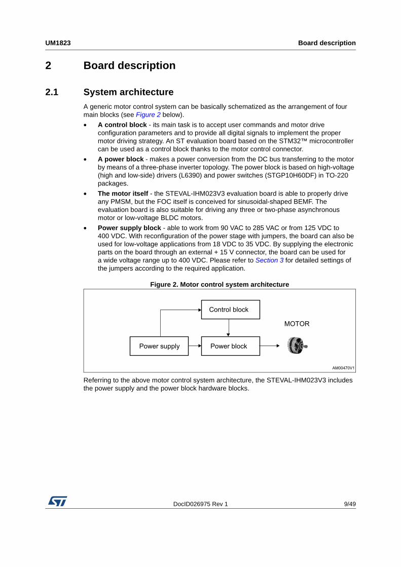
2.1 System architectureA generic motor control system can be basically schematized as the arrangement of four main blocks (see Figure 2 below).
• A control block - its main task is to accept user commands and motor drive configuration parameters and to provide all digital signals to implement the proper motor driving strategy. An ST evaluation board based on the STM32™ microcontroller can be used as a control block thanks to the motor control connector.
• A power block - makes a power conversion from the DC bus transferring to the motor by means of a three-phase inverter topology. The power block is based on high-voltage (high and low-side) drivers (L6390) and power switches (STGP10H60DF) in TO-220 packages.
• The motor itself - the STEVAL-IHM023V3 evaluation board is able to properly drive any PMSM, but the FOC itself is conceived for sinusoidal-shaped BEMF. The evaluation board is also suitable for driving any three or two-phase asynchronous motor or low-voltage BLDC motors.
• Power supply block - able to work from 90 VAC to 285 VAC or from 125 VDC to 400 VDC. With reconfiguration of the power stage with jumpers, the board can also be used for low-voltage applications from 18 VDC to 35 VDC. By supplying the electronic parts on the board through an external + 15 V connector, the board can be used for a wide voltage range up to 400 VDC. Please refer to Section 3 for detailed settings of the jumpers according to the required application.
Figure 2. Motor control system architecture
Referring to the above motor control system architecture, the STEVAL-IHM023V3 includes the power supply and the power block hardware blocks.

Board description UM1823
10/49 DocID026975 Rev 1
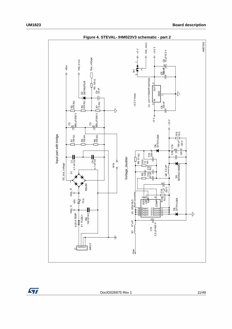
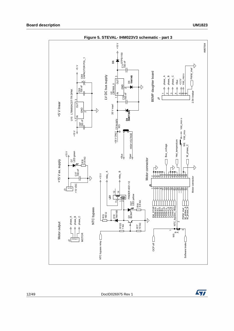
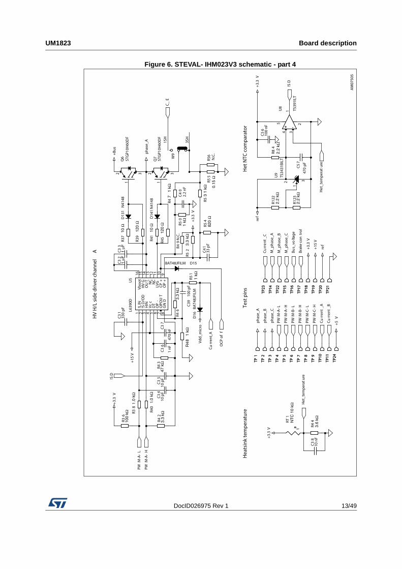
2.2 The board schematic
Figure 3. STEVAL- IHM023V3 schematic - part 1
H1/
A+
H2/
B+H
3/Z+
+ 3
.3/5
VG
ND
Hal
l/en
code
r
AB
Tach
o se
nsor
Brak
e co
ntro
lM_p
has
e_A
M_p
has
e_B
M_p
has
e_C
M_p
has
e_A
volta
ge o
ff
Brak
e co
ntro
l
Soft
war
e br
ake
volta
ge o
ff
Vdd_
mic
ro
+5
V
Vdd_
mic
ro
Vdd_
mic
ro
+15
V
+15
V
+15
V
+15
V+
Bus
+Bu
s
+15
V
Q14
BC84
7
M74
HC1
4M1R
U11
B
34
R18
R27
- +
U4
TS39
1ILT
- +
13 4
5 2
Q3
STG
P10H
60D
F
R117
Q4
BC84
7
R24
C2
92.
2 nF
J4
Enco
der/
hall
J41 2 3 4 5
M74
HC
14M
1RU
11C
56
C6
510
0pF
D2
6ST
TH2L
06
R107
Q1
2
BC84
7
C7
110
0 nF
D2
5BZ
X84
B13V
R32
R109
R21
J6 R Br
ake
12
Q1
8BC
847
C2
810
0 n
F
C7
410
pF
J8 Tach
o
1 2
M74
HC
14M
1RU
11D
98
W4
H1/
A+
R104
C75 1n
FC
75 1nF
R110
R28
R34
R29
R30
W1
6
12
3
U11
EM
74H
C14
M1R
1110
C7
210
0 nF
Q1
3
BC84
7
C7
010
pF
R112
R31
Q5
BC84
7
+
C2
5
+
R26
R111
C2
710
0 nF
R115
R121
R105
R120
5.
M74
HC
14M
1RU
11F
1312
14
7
D2
8LE
D R
ed
R25
C6
910
pF
R20
D2
9B
ZX84
B13V
Q16
BC84
7
Q2
BC85
7B
W7
Tach
o
R113
C3
0
4.7
nF
C2
610
0 nF
C2
410
0 nF
C7
310
0 nF
R106
220R
M74
HC
14M
1RU
11A
12
R33
R22
R19
N.C
.
R35
R116
R114
Q1
7BC
847
Q1
5BC
847
1
BAT48JFILM
D1
R23
2
BAT48JFILM
D1
AM
0750
2
DocID026975 Rev 1 11/49
UM1823 Board description
49
Figure 4. STEVAL- IHM023V3 schematic - part 2
Inpu
t par
t with
brid
ge
DC
_bus
_vol
tage
Buc
k co
nver
ter
+3.
3 V
line
ar
Bus
_vol
tage
Vdd
_mic
ro
+Bus
rela
y_B
rela
y_A
+15
V
Vdd
_m
icro
+5 V
+3.3
V
+5V
Vip
er
+C
8/6
.3+
V
+C
15 /450
V
+
W1
1
2
3
R12
D6
ST
TH
1L06
A
+C
19 /25
V
+
VR
1
R3
U1
LD11
17S
33T
R S
OT
223
GN
D
1
IN3
OU
T2
+C
3
/250
V
+
R10
D8
ST
TH
1L06
A
R10
8
+C
2
/250
V
+
R4
C7
100
nFC
710
0 nF
C14 220
nF
-+
D1
KB
U6K
-+
R1
C12
47 n
F
R7
C6
100
nF
D9
BZ
V55
C18
SM
D
R8C1
4.7
nF/Y
2
4.7
nF/Y
2
W14
tage
_dou
Vol
bler
L1L1
C13
N.C
.
C9
10 n
F
R6
U3
VIP
er16
LD
VD
D5
FB
7
Source1 1Source2 2
Drain116Drain215Drain314Drain413
Source3 3Source4 4
LIM
6
CO
MP
8
R9
R2
C4
/X2
C4
150
nF
C5
R5
C18
100
nF
L2H
L2
F1
FU
SE
-1
6.25
A T
EM
P
+C
16 /50
V
+
J1 INP
UT
1234D
2B
AT
48JF
ILM
AM
0750
3
N.C
.
N.C
.
Board description UM1823
12/49 DocID026975 Rev 1
Figure 5. STEVAL- IHM023V3 schematic - part 3
DocID026975 Rev 1 13/49
UM1823 Board description
49
Figure 6. STEVAL- IHM023V3 schematic - part 4
HV
H/L
sid
e dr
iver
cha
nnel
A
Hea
tsin
k te
mpe
ratu
reTe
st p
ins
Het
NTC
com
para
tor
3SH
PWM
-A-
H
PWM
-A-
L
Cu
rren
t_A
OC
P of
f
!SD
Het
_tem
pera
ture
PWM
-A-H
PWM
-A-L
PWM
-B-H
PWM
-B-L
PWM
-C-H
PWM
-C-L
Cu
rren
t_A
Cu
rren
t_B
Brak
e co
ntr
ol
M_p
has
e_A
M_p
has
e_B
M_p
has
e_C
Bus_
volta
ge
Cu
rren
t_C
!SD
Het
_tem
pera
tur
e
C_
E
+3.
3V
Vdd_
mic
ro
+Bu
s
+15
V
phas
e_A
+3.
3V
+3.
3 V
phas
e_A
phas
e_B
phas
e_C
ref
+15
V
+3.
3 V
ref
+3.
3V
+5
VD16
BAT4
8JFI
LM
TP1
TP1
R56
N.C
.
TP22
TP22
R4
U9
TS34
31BI
LT
32
1
C3
2
TP17
TP17
-+U
8
TS39
1ILT
-+1
345 2
TP2
TP2
C3
6
1 nF
TP23
TP23
D14
1N
4148
D15BAT48JFILM
R39
TP9
TP9
R49
N.C
.
R5
C5
610
0 nF
R42
C3
510
pF
R50
C3
3
R41
TP8
TP8
C39
100
pF
Q6
STG
P10H
60D
F1
2 3
R36
TP21
TP21
RT1
tTP
16TP
16
C5
7
470
pF
TP7
TP7
C3
7
470
nF
C3
133
0 pF
Q7
STG
P10H
60D
F1
2 3
R51
D13
1N
4148
R54
R122
R52
TP18
TP18
R40
TP6
TP6
R44
TP10
TP10
TP24
TP24
R55
R84
TP4
TP4
U5
L639
0D
DT
5
OPO
UT
7
!LIN
1!S
D/O
D2
Vboo
t16
HV
G15
HIN
3Vc
c4
OP
-6
CP
+10
GN
D8
OP
+9
OU
T14
LVG
11N
C12
NC
13
R38
1
R46
TP15
TP15
TP11
TP11
C4
02.
2 nF
C4
133
pF
R37
R123
R43 TP
5TP
5
C3
810
nF
TP3
TP3
C3
410
pF
W9
1SH
TP20
TP20
TP14
TP14
R45
TP19
TP19
AM
0750
5
1
Board description UM1823
14/49 DocID026975 Rev 1
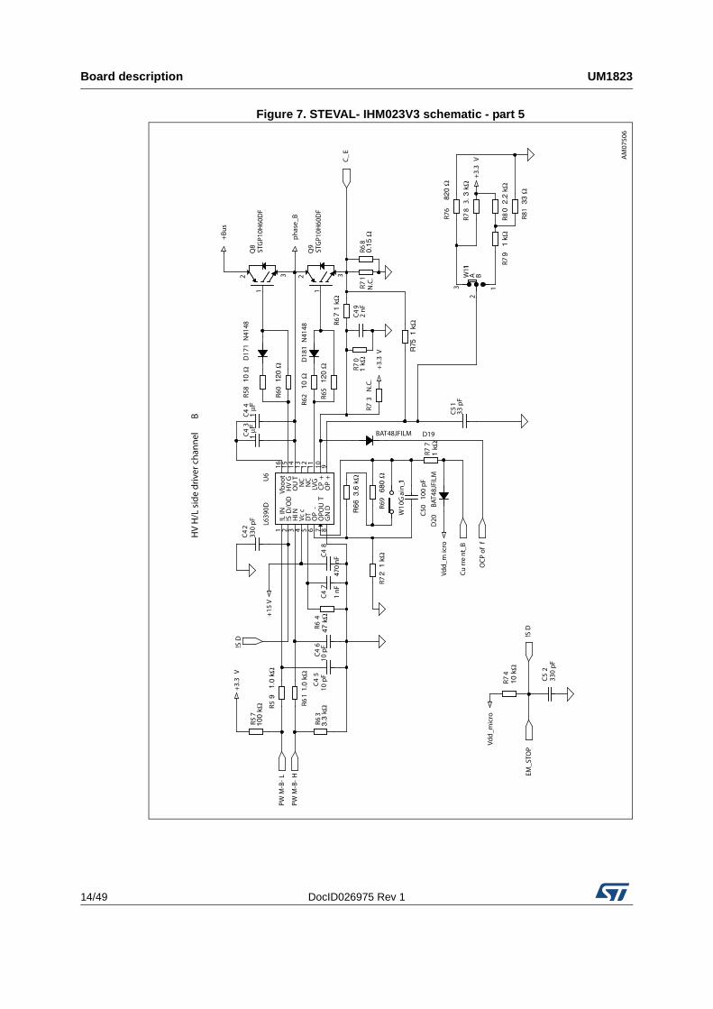
Figure 7. STEVAL- IHM023V3 schematic - part 5
A B
HV
H/L
sid
e dr
iver
cha
nnel
B
!SD
OC
P of
f
!SD
EM_S
TOP
PWM
-B-
H
PWM
-B-
L
Curr
ent
_B
C_
E
Vdd_
mic
ro
Vdd_
mic
ro
+3.
3 V
+3.
3 V
+Bu
s
+15
V
phas
e_B
+3.
3V
C4
3
R6
C50
100
pF
R71
N.C
.
C4
233
0 pF
R8
R62
R76
Q9
STG
P10H
60D
F1
2 3
D18
1N
4148
R63
R5
C5
233
0 pF
R73
N.C
.
R77
D17
1N
4148
R78
3.
C4
92
nF
R57
R68
C4
510
pF
R69
U6
L639
0D
DT
5
OPO
UT
7
!LIN
1
!SD
/OD
2Vb
oot
16
HV
G15
HIN
3
Vcc
4
OP
-6
CP
+10
GN
D8
OP
+9
OU
T14
LVG
11N
C12
NC
13
Q8
STG
P10H
60D
F1
2 3
R61
1
W1
0Gai
n_11
C4
7
1 nF
R58
R70
R64
R7
C4
610
pF
R74
D20
BAT4
8JFI
LM
R65
C5
133
pF
R7
W111
1
2
3
C4
4
R81
D19BAT48JFILM
C4
8
470
nF
R60
AM
0750
6
DocID026975 Rev 1 15/49
UM1823 Board description
49
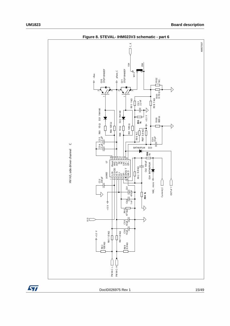
Figure 8. STEVAL- IHM023V3 schematic - part 6
HV
H/L
sid
e dr
iver
cha
nnel
C
3SH
!SD
OC
P of
f
PWM
-C-
H
PWM
-C-
L
Cu
rre
nt_C
C_
E
Vdd_
mic
ro
+3.3
V
+Bus
+15
V
phas
e_C
+3.3
V
R85
1
C62
100
pF
R88
Q1
STG
P10H
60D
F0
1
2 3
R87
1
R96
N.C
.
C5
810
pF
R98
1kR98
1k
D21
1N
4148
R90
R102
N.C
.
D23BAT48JFILM
U7
L639
0D DT
5
OPO
UT
7
!LIN
1
!SD
/OD
2Vb
oot
16
HVG
15
HIN
3
Vcc
4
OP
-6
CP
+10
GN
D8
OP
+9
OU
T14
LVG
11N
C12
NC
13
R92
C6
32.
2 nF
C6
0
1 nF
R83
W1
3
1SH
C5
910
pF
R91
C5
4
D24
BAT4
8JFI
LM
C5
5
Q11
STG
P10H
60D
F1
2 3
D2
21N
4148
R89
C6
433
pF
C61
470
nF
R93
1kR93
1k
C5
333
0 pF
R94
1kR9
41k
R86
R9
R82
R101
R95
1
R100
AM
0750
7

Board description UM1823
16/49 DocID026975 Rev 1
2.3 Circuit description
2.3.1 Power supply
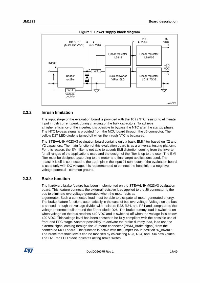
The power supply in the STEVAL-IHM023V3 evaluation board is implemented as a multifunctional block which allows to supply the inverter in all ranges of input voltage up to 285 VAC or 400 VDC. If the input AC voltage does not surpass 145 VAC, it is possible to apply the input voltage doubler, this is done by shorting the W14 jumper. This configuration almost doubles the input AC voltage to a standard level and allows to evaluate the motor control application with a low level of input AC voltage.
For high-voltage applications it is necessary to set W3 jumpers to position “HIGH VOLTAGE”, the auxiliary power supply for supplying all active components on the evaluation board is implemented as a buck converter based on the U6 VIPer16L which works with fixed frequency 60 kHz. The output voltage of the converter is +15 VDC voltage which is fed into the L6390 drivers as supply voltage as well as into the linear regulator L78L33ACD and L78M05ACDT. The linear regulator provides +3.3 VDC and +5 VDC for supplying the operational amplifiers and other related parts placed on the evaluation board. The selection of supply voltage for hardware peripherals placed on the board is done with jumper W1. In the “3.3 V” position the supply voltage selected is +3.3 V and in the “5 V” position it is +5 V. Thanks to jumper W6, it is possible to supply the connected MCU driving board with related supply voltage. In this case, the maximal consumptive current of the MCU unit has not overreached 50 mA. Please refer to the ST released VIPer16LD datasheet for further information on this concept.
For low-voltage applications, the step-down converter must be disabled by setting the W3 jumper to position “<35 V ONLY”. In this case, the other linear regulator, L7815, is connected directly on the bus line, to provide auxiliary voltage + 15 VDC.
Note: Please note that the voltage range in this kind of application must be in the range + 18 VDC to + 35 VDC.
For low-voltage DC motor applications which require a voltage lower than + 18 VDC, a dual supply mode can be used. Voltage on the input connector is normally linked through power switches to the motor and an external auxiliary voltage is fed through the J3 connector from an external power source. The voltage of the external power supply used must be in the range + 14.8 V to + 15.5 V with maximal consumption current 0.5 A.
The information regarding the value of the supply bus voltage on the main filtering capacitors is sensed with the voltage divider built around R2, R4, and R7 and is fed into the dedicated control unit through the J5 connector. The proper voltage partitioning for applied resistors values is 0.0075.
The presence of +15 VDC on the board is indicated with green LED D7. For a better understanding of the concept, Figure 9 describes the power supply in a block diagram.
DocID026975 Rev 1 17/49
UM1823 Board description
49
Figure 9. Power supply block diagram
2.3.2 Inrush limitation
The input stage of the evaluation board is provided with the 10 Ω NTC resistor to eliminate input inrush current peak during charging of the bulk capacitors. To achieve a higher efficiency of the inverter, it is possible to bypass the NTC after the startup phase. The NTC bypass signal is provided from the MCU board through the J5 connector. The yellow D27 LED diode is turned off when the inrush NTC is bypassed.
The STEVAL-IHM023V3 evaluation board contains only a basic EMI filter based on X2 and Y2 capacitors. The main function of this evaluation board is as a universal testing platform. For this reason, the EMI filter is not able to absorb EMI distortion coming from the inverter for all ranges of the applications used and the design of the filter is up to the user. The EMI filter must be designed according to the motor and final target applications used. The heatsink itself is connected to the earth pin in the input J1 connector. If the evaluation board is used only with DC voltage, it is recommended to connect the heatsink to a negative voltage potential - common ground.
2.3.3 Brake function
The hardware brake feature has been implemented on the STEVAL-IHM023V3 evaluation board. This feature connects the external resistive load applied to the J6 connector to the bus to eliminate overvoltage generated when the motor acts as a generator. Such a connected load must be able to dissipate all motor generated energy. The brake feature functions automatically in the case of bus overvoltage. Voltage on the bus is sensed through the voltage divider with resistors R23, R24, and R31 and compared to the voltage reference built around the Zener diode D26. The brake dummy load is switched on when voltage on the bus reaches 440 VDC and is switched off when the voltage falls below 420 VDC. This voltage level has been chosen to be fully compliant with the possible use of front-end PFC stage. Another possibility, to activate the brake dummy load, is to use the external signal coming through the J5 motor connector (PWM_Brake signal) from the connected MCU board. This function is active with the jumper W5 in position “R_BRAKE”. The brake threshold levels can be modified by calculating R23, R24, and R34 new values. The D28 red LED diode indicates acting brake switch.
Board description UM1823
18/49 DocID026975 Rev 1
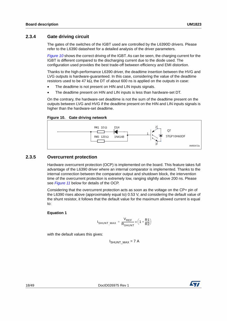
2.3.4 Gate driving circuit
The gates of the switches of the IGBT used are controlled by the L6390D drivers. Please refer to the L6390 datasheet for a detailed analysis of the driver parameters.
Figure 10 shows the correct driving of the IGBT. As can be seen, the charging current for the IGBT is different compared to the discharging current due to the diode used. The configuration used provides the best trade-off between efficiency and EMI distortion.
Thanks to the high-performance L6390 driver, the deadtime insertion between the HVG and LVG outputs is hardware-guaranteed. In this case, considering the value of the deadtime resistors used to be 47 kΩ, the DT of about 600 ns is applied on the outputs in case:
• The deadtime is not present on HIN and LIN inputs signals.
• The deadtime present on HIN and LIN inputs is less than hardware-set DT.
On the contrary, the hardware-set deadtime is not the sum of the deadtime present on the outputs between LVG and HVG if the deadtime present on the HIN and LIN inputs signals is higher than the hardware-set deadtime.
Figure 10. Gate driving network
2.3.5 Overcurrent protection
Hardware overcurrent protection (OCP) is implemented on the board. This feature takes full advantage of the L6390 driver where an internal comparator is implemented. Thanks to the internal connection between the comparator output and shutdown block, the intervention time of the overcurrent protection is extremely low, ranging slightly above 200 ns. Please see Figure 11 below for details of the OCP.
Considering that the overcurrent protection acts as soon as the voltage on the CP+ pin of the L6390 rises above (approximately equal to) 0.53 V, and considering the default value of the shunt resistor, it follows that the default value for the maximum allowed current is equal to:
Equation 1
with the default values this gives:
ISHUNT_MAX = 7 A
D14
1N41481
2
3
Q7
R45 120 Ω
R41 10 Ω
AM00472a
STGP10H60DF
ISHUNT MAX
VREF
RSHUNT---------------------- 1 R1
R2--------+
×=

DocID026975 Rev 1 19/49
UM1823 Board description
49
Figure 11. Overcurrent protection
The overcurrent protection can be disabled with software if the W5 jumper is set to the “OCP OFF” position. This may be necessary and is often useful when the user decides to make the brake operate by turning on the three low-side switches. In fact, if the motor acts as a generator, it's necessary to protect the hardware, preventing the bus voltage from exceeding a safety threshold. In addition to dissipating the motor energy on a brake resistor, it's possible to short the motor phases, preventing the motor current from flowing through the bulk capacitors.
Please note that with disabling of the OCP, the evaluation board is not protected against any overcurrent event.
2.3.6 Current sensing amplifying network
The STEVAL-IHM023V3 motor control evaluation board can be configured to run in various current reading configuration modes:
• Three-shunt configuration - suitable for the use of field oriented control (FOC)
• Single-shunt configuration - suitable for the use of FOC in a single-shunt configuration
• Single-shunt six-step configuration - suitable for scalar control
Configuration with a shunt resistor, where voltage amplified with an operational amplifier is sensed, was chosen as the current sensing networks. Single-shunt configuration requires a single op amp, three-shunt configuration requires three op amps. Just for compatibility purposes, one of them is common to both basic configurations.
The configuration jumpers W10 and W11 allow the user to set the common op amp to achieve the compatibility between single-shunt six-step configuration (suitable for scalar control) and three-shunt or single-shunt FOC current reading configuration.
Three-shunt FOC or single-shunt FOC current reading configuration
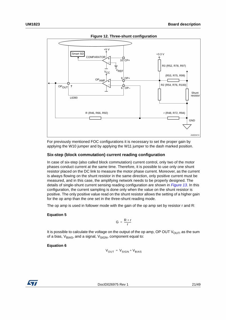
The details of the three-shunt current sensing reading configuration are shown in Figure 12. In this configuration, the alternating signal on the shunt resistor, with positive and negative
–+
Shuntresistor
VREF
COMPARATOR
+5 V
L6390
OPAMP
+
6
9
7
10
OP+
CP+
OP–
+3.3 V
R3 (R49, R73, R96)
R1 (R47, R67, R95)
R2 (50, R70, R93)
Smart SD
VCC
–
OPOUT
9
GND
AM00473

Board description UM1823
20/49 DocID026975 Rev 1
values, must be converted to be compatible with the single positive input of the microcontroller A/D converter used to read the current value. This means that the op amp must be polarized in order to obtain a voltage on the output that makes it possible to measure the symmetrical alternating input signal.
The op amp is used in follower mode with the gain of the op amp set by resistor r and R:
Equation 2
It is possible to calculate the voltage on the output of the op amp, OP OUT - VOUT, as the sum of a bias, VBIAS, and a signal, VSIGN, component equal to:
Equation 3
Total gain of the circuit including the resistors’ divider is equal to:
Equation 4
with the default values this gives:
• VBIAS = 1.7 V
• G = 4.3
• GTOT = 1.7
• Maximum current amplifiable without distortion is 6.5 A.
Please observe that the user can modify the max. current value by changing the values of the shunt resistors.
G R r+r
------------=
VOUT VSIGN VBIAS+=
VBIAS3.3
1R1--------
1R2--------
1R3--------+ +
R3×--------------------------------------------------------- G×=
VSIGN
I RSHUNT×
1R1--------
1R2--------
1R3--------+ +
R1×--------------------------------------------------------- G×=
GTOT
VSIGN
VIN----------------
VSIGN
RSHUNT I×----------------------------= =
DocID026975 Rev 1 21/49
UM1823 Board description
49
Figure 12. Three-shunt configuration
For previously mentioned FOC configurations it is necessary to set the proper gain by applying the W10 jumper and by applying the W11 jumper to the dash marked position.
Six-step (block commutation) current reading configuration
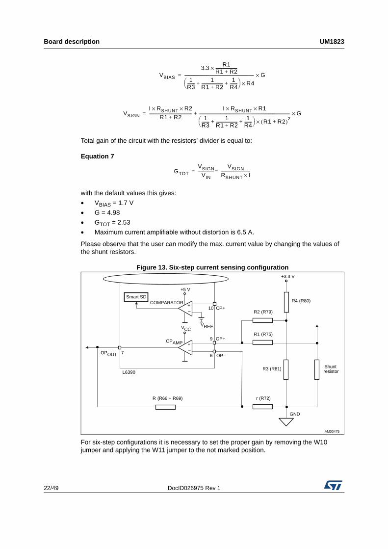
In case of six-step (also called block commutation) current control, only two of the motor phases conduct current at the same time. Therefore, it is possible to use only one shunt resistor placed on the DC link to measure the motor phase current. Moreover, as the current is always flowing on the shunt resistor in the same direction, only positive current must be measured, and in this case, the amplifying network needs to be properly designed. The details of single-shunt current sensing reading configuration are shown in Figure 13. In this configuration, the current sampling is done only when the value on the shunt resistor is positive. The only positive value read on the shunt resistor allows the setting of a higher gain for the op amp than the one set in the three-shunt reading mode.
The op amp is used in follower mode with the gain of the op amp set by resistor r and R:
Equation 5
It is possible to calculate the voltage on the output of the op amp, OP OUT VOUT, as the sum of a bias, VBIAS, and a signal, VSIGN, component equal to:
Equation 6
+
Shunt resistor
Smart SD
VREF
COMPARATOR
VCC
L6390
OPAMP
+
OPOUT 6
9
7
10
OP+
CP+
OP
GND
+3.3 V
R3 (R52, R78, R97)
(R53, R75, R99)
R2 (R54, R76, R100)
r (R48, R72, R94)R (R46, R66, R92)
–+
+5 V
–+
7–
AM00474
G R r+r
------------=
VOUT VSIGN VBIAS+=
Board description UM1823
22/49 DocID026975 Rev 1
Total gain of the circuit with the resistors’ divider is equal to:
Equation 7
with the default values this gives:
• VBIAS = 1.7 V
• G = 4.98
• GTOT = 2.53
• Maximum current amplifiable without distortion is 6.5 A.
Please observe that the user can modify the max. current value by changing the values of the shunt resistors.
Figure 13. Six-step current sensing configuration
For six-step configurations it is necessary to set the proper gain by removing the W10 jumper and applying the W11 jumper to the not marked position.
VBIAS
3.3 R1R1 R2+----------------------×
1R3--------
1R1 R2+----------------------
1R4--------+ +
R4×----------------------------------------------------------------------- G×=
VSIGN
I RSHUNT R2××R1 R2+
--------------------------------------------I RSHUNT R1××
1R3--------
1R1 R2+----------------------
1R4--------+ +
R1 R2+( )2×--------------------------------------------------------------------------------------------- G×+=
GTOT
VSIGN
VIN----------------
VSIGN
RSHUNT I×------------------------------==
–+
Shunt resistor
Smart SD
VREF
COMPARATOR
+5 V
VCC
L6390
OPAMP
–+
OPOUT 6
9
7
10
OP+
CP+
OP–
GND
+3.3 V
R1 (R75)
R3 (R81)
r (R72)R (R66 + R69)
R2 (R79)
R4 (R80)
AM00475
DocID026975 Rev 1 23/49
UM1823 Board description
49
In Table 1 the mentioned setting of gain jumpers, for all possible current reading configurations, is shown.
2.3.7 The tachometer and Hall/encoder inputs
Both the tachometer and Hall/encoder inputs have been implemented on the board. In the case of using a Hall or encoder sensor, the W4 jumper must be connected and the W7 jumper disconnected. The W16 jumper set to dash marked “-” position allows to supply any connected Hall sensor with +5 VDC supply voltage. Setting the W16 jumper to not marked position supplies the Hall sensor with the same supply voltage as other hardware peripherals (+3.3 VDC or +5 VDC depend on the W1 jumper). The U11 Hex Schmitt inverter is used as the voltage level shifter for the connected Hall sensor.
In the case of using a tachometer, the W4 jumper must be disconnected and the W7 jumper connected.This feature allows to test and evaluate a wide spectrum of various motors.
2.3.8 Temperature feedback and overtemperature protection
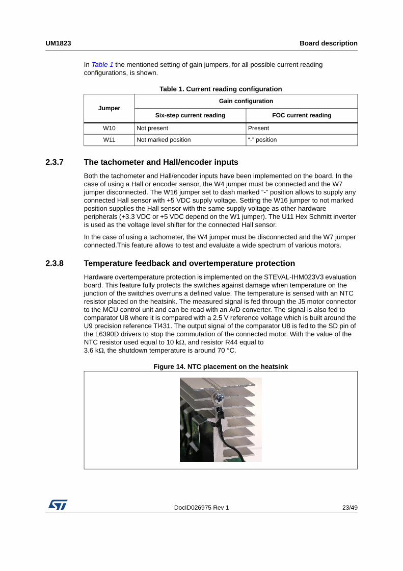
Hardware overtemperature protection is implemented on the STEVAL-IHM023V3 evaluation board. This feature fully protects the switches against damage when temperature on the junction of the switches overruns a defined value. The temperature is sensed with an NTC resistor placed on the heatsink. The measured signal is fed through the J5 motor connector to the MCU control unit and can be read with an A/D converter. The signal is also fed to comparator U8 where it is compared with a 2.5 V reference voltage which is built around the U9 precision reference Tl431. The output signal of the comparator U8 is fed to the SD pin of the L6390D drivers to stop the commutation of the connected motor. With the value of the NTC resistor used equal to 10 kΩ, and resistor R44 equal to 3.6 kΩ, the shutdown temperature is around 70 °C.
Figure 14. NTC placement on the heatsink
Table 1. Current reading configuration
JumperGain configuration
Six-step current reading FOC current reading
W10 Not present Present
W11 Not marked position “-” position
Hardware setting of the STEVAL-IHM023V3 UM1823
24/49 DocID026975 Rev 1
3 Hardware setting of the STEVAL-IHM023V3
The STEVAL-IHM023V3 evaluation board can be driven through the J5 motor control connector by various MCU control units released by STMicroelectronics which feature a unified 34-pin motor connector. The evaluation board is suitable for both field oriented and scalar controls. In particular, it can handle output signal conditioning for different types of speed and/or position feedback sensors (such as tachometer, Hall sensors, and quadrature encoders) and different current sensing topologies (single-shunt resistor placed on DC bus or three-shunt resistors placed in the three inverter legs).
3.1 Hardware settings for six-step (block commutation) control of BLDC motorsTo drive any motor, the user must ensure that:
• The motor control evaluation board is driven by a control board that provides the six output signals required to drive the three-phase power stage
• The motor is connected to the J2 motor output connector
• If using an encoder or Hall sensor connection, it is connected to connector J4
• If using a tachometer connection, it is connected to connector J8
• If using the brake control feature, connect a dissipative power load to J6 connector
Table 2 below shows the jumper settings for any BLDC high-voltage motors in six-step (block commutation) control. Please confirm that the evaluation board input voltage is in the range of 125 VDC to 400 VDC or 90 VAC to 285 VAC. If the voltage doubler is applied, the input voltage must be in the range of 65 VAC to 145 VAC.
Table 2. Jumper settings for high-voltage BLDC motor in six-step control
Jumper Settings for any HV motor in six-step control
W1“3.3 V” position for VDD = 3.3 V
“5 V” position for VDD = 5 V
W3 “HIGH VOLTAGE” position
W4Present for Hall sensor or encoder
Not present for connected tachometer
W5“R_BRAKE” position for software handling of resistive brake (if any)
“OCP OFF” position for software handling of overcurrent protection disabling
W6 Present for supplying stage from IHM023V2 (max. 50 mA)
W7Present for connected tachometer
Not present for connected Hall sensor or encoder
W9 Single-shunt
W10 Not present
W11 Not marked position
W13 Single-shunt
DocID026975 Rev 1 25/49
UM1823 Hardware setting of the STEVAL-IHM023V3
49
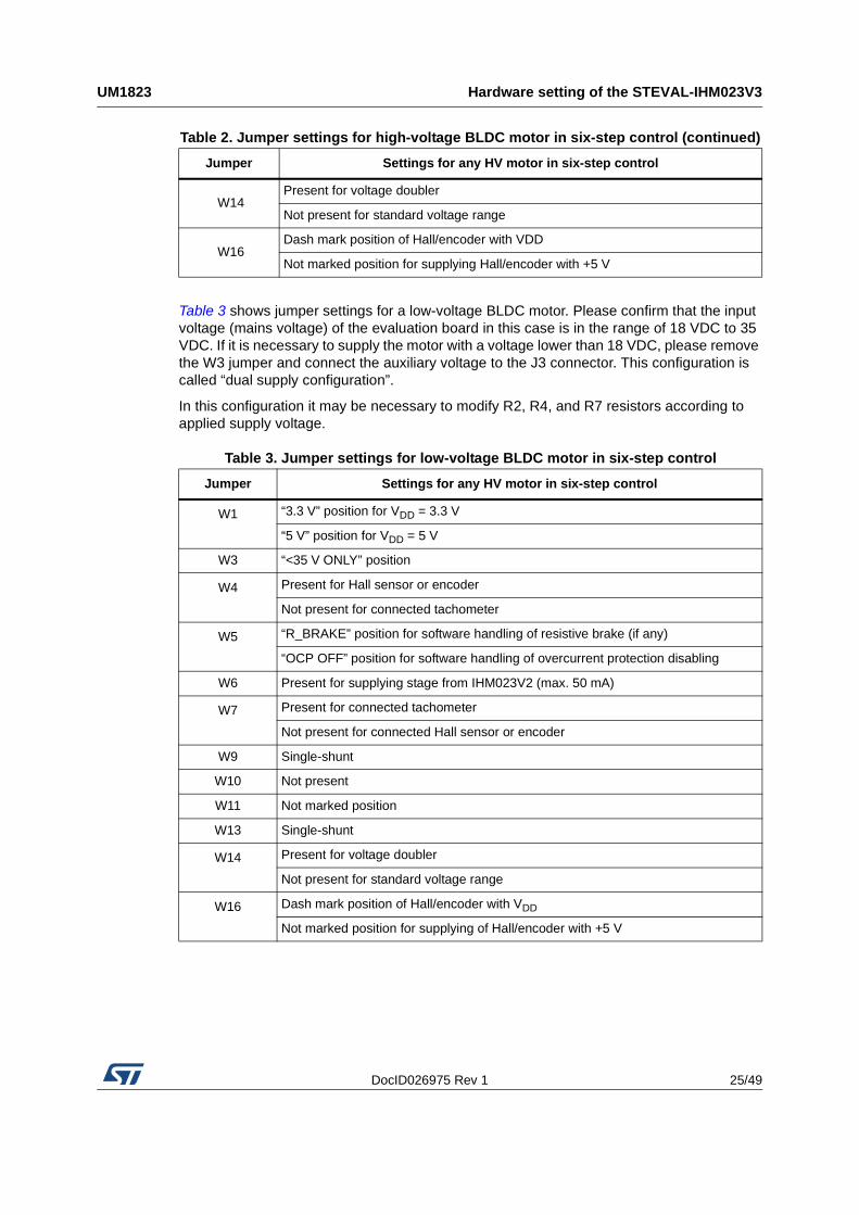
Table 3 shows jumper settings for a low-voltage BLDC motor. Please confirm that the input voltage (mains voltage) of the evaluation board in this case is in the range of 18 VDC to 35 VDC. If it is necessary to supply the motor with a voltage lower than 18 VDC, please remove the W3 jumper and connect the auxiliary voltage to the J3 connector. This configuration is called “dual supply configuration”.
In this configuration it may be necessary to modify R2, R4, and R7 resistors according to applied supply voltage.
W14Present for voltage doubler
Not present for standard voltage range
W16Dash mark position of Hall/encoder with VDD
Not marked position for supplying Hall/encoder with +5 V
Table 3. Jumper settings for low-voltage BLDC motor in six-step control
Jumper Settings for any HV motor in six-step control
W1
“3.3 V” position for VDD = 3.3 V
“5 V” position for VDD = 5 V
W3 “<35 V ONLY” position
W4
Present for Hall sensor or encoder
Not present for connected tachometer
W5
“R_BRAKE” position for software handling of resistive brake (if any)
“OCP OFF” position for software handling of overcurrent protection disabling
W6 Present for supplying stage from IHM023V2 (max. 50 mA)
W7
Present for connected tachometer
Not present for connected Hall sensor or encoder
W9 Single-shunt
W10 Not present
W11 Not marked position
W13 Single-shunt
W14
Present for voltage doubler
Not present for standard voltage range
W16
Dash mark position of Hall/encoder with VDD
Not marked position for supplying of Hall/encoder with +5 V
Table 2. Jumper settings for high-voltage BLDC motor in six-step control (continued)
Jumper Settings for any HV motor in six-step control
Hardware setting of the STEVAL-IHM023V3 UM1823
26/49 DocID026975 Rev 1
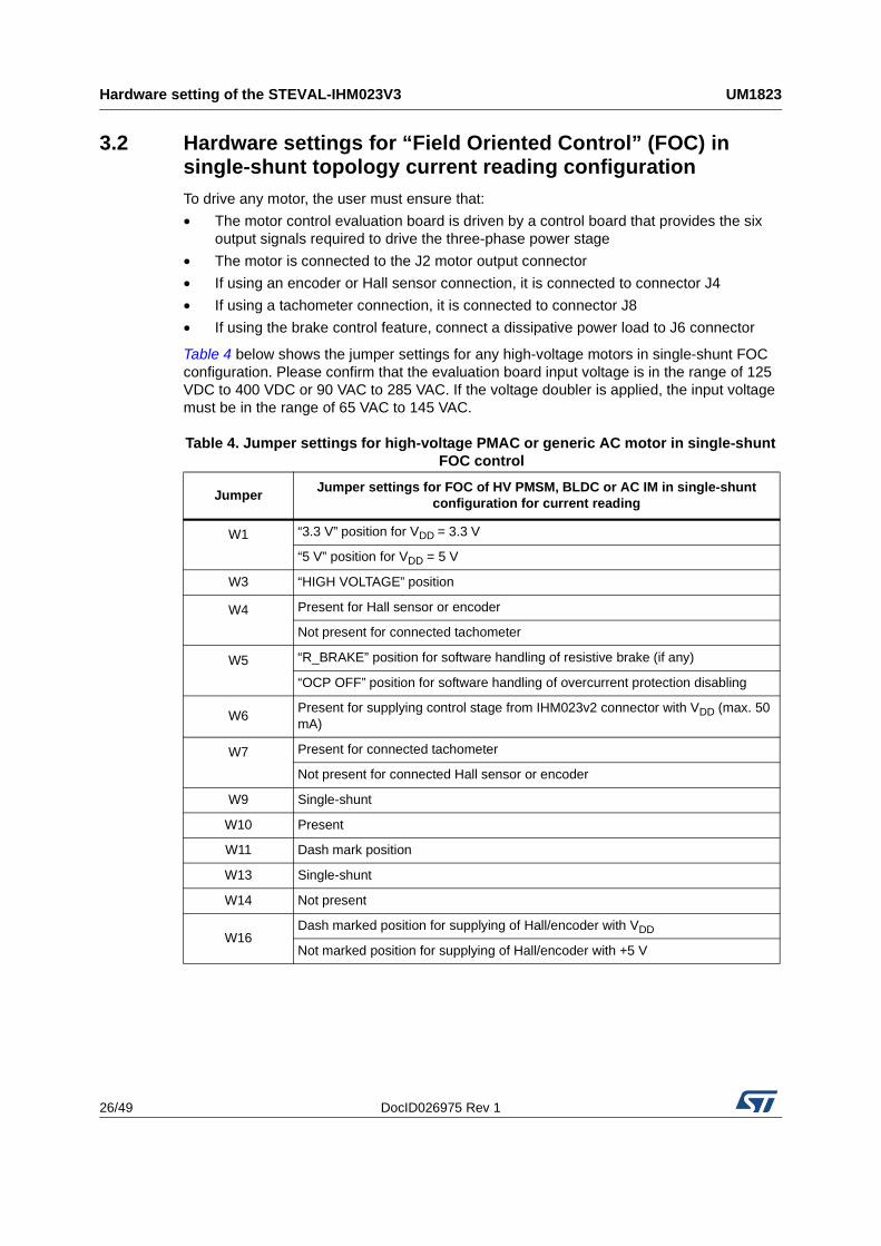
3.2 Hardware settings for “Field Oriented Control” (FOC) in single-shunt topology current reading configurationTo drive any motor, the user must ensure that:
• The motor control evaluation board is driven by a control board that provides the six output signals required to drive the three-phase power stage
• The motor is connected to the J2 motor output connector
• If using an encoder or Hall sensor connection, it is connected to connector J4
• If using a tachometer connection, it is connected to connector J8
• If using the brake control feature, connect a dissipative power load to J6 connector
Table 4 below shows the jumper settings for any high-voltage motors in single-shunt FOC configuration. Please confirm that the evaluation board input voltage is in the range of 125 VDC to 400 VDC or 90 VAC to 285 VAC. If the voltage doubler is applied, the input voltage must be in the range of 65 VAC to 145 VAC.
Table 4. Jumper settings for high-voltage PMAC or generic AC motor in single-shunt FOC control
JumperJumper settings for FOC of HV PMSM, BLDC or AC IM in single-shunt
configuration for current reading
W1
“3.3 V” position for VDD = 3.3 V
“5 V” position for VDD = 5 V
W3 “HIGH VOLTAGE” position
W4
Present for Hall sensor or encoder
Not present for connected tachometer
W5
“R_BRAKE” position for software handling of resistive brake (if any)
“OCP OFF” position for software handling of overcurrent protection disabling
W6Present for supplying control stage from IHM023v2 connector with VDD (max. 50 mA)
W7
Present for connected tachometer
Not present for connected Hall sensor or encoder
W9 Single-shunt
W10 Present
W11 Dash mark position
W13 Single-shunt
W14 Not present
W16 Dash marked position for supplying of Hall/encoder with VDD
Not marked position for supplying of Hall/encoder with +5 V

DocID026975 Rev 1 27/49
UM1823 Hardware setting of the STEVAL-IHM023V3
49
Table 5 shows jumper settings for a low-voltage BLDC motor in single-phase FOC current control. Please confirm that the input voltage (mains voltage) of the evaluation board in this case is in the range of 18 VDC to 35 VDC. If it is necessary to supply the motor with a voltage lower than 18 VDC, please remove the W3 jumper and connect the auxiliary voltage to the J3 connector.
In this configuration it may be necessary to modify R2, R4, and R7 resistors according to applied supply voltage.
3.3 Hardware settings for FOC in three-shunt configurationTo drive any motor, the user must ensure that:
• The motor control evaluation board is driven by a control board that provides the six outputs signals required to drive the three-phase power stage
• The motor is connected to the J4 motor output connector
• If using an encoder or Hall sensor connection, it is connected to connector J5
• If using a tachometer connection, it is connected to connector J6
• If using the brake control feature, connect a dissipative power load to J7 connector
Table 5. Jumper settings for low-voltage BLDC motor in single-shunt FOC control
Jumper Settings for any LV BLDC motor in single-shunt FOC control
W1
“3.3 V” position for VDD = 3.3 V
“5 V” position for VDD = 5 V
W3 “<35 V ONLY” position
W4
Present for Hall sensor or encoder
Not present for connected tachometer
W5
“R_BRAKE” position for software handling of resistive brake (if any)
“OCP OFF” position for software handling of overcurrent protection disabling
W6Present for supplying control stage from IHM023v2 connector with VDD (max. 50 mA)
W7
Present for connected tachometer
Not present for connected Hall sensor or encoder
W9 Single-shunt
W10 Present
W11 Dash mark position
W13 Single-shunt
W14 Not present
W16
Dash marked position for supplying of Hall/encoder with VDD
Not marked position for supplying of Hall/encoder with +5 V
Hardware setting of the STEVAL-IHM023V3 UM1823
28/49 DocID026975 Rev 1
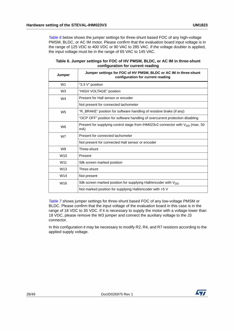
Table 6 below shows the jumper settings for three-shunt based FOC of any high-voltage PMSM, BLDC, or AC IM motor. Please confirm that the evaluation board input voltage is in the range of 125 VDC to 400 VDC or 90 VAC to 285 VAC. If the voltage doubler is applied, the input voltage must be in the range of 65 VAC to 145 VAC.
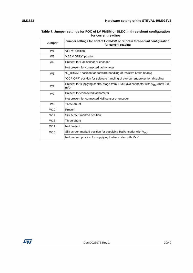
Table 7 shows jumper settings for three-shunt based FOC of any low-voltage PMSM or BLDC. Please confirm that the input voltage of the evaluation board in this case is in the range of 18 VDC to 35 VDC. If it is necessary to supply the motor with a voltage lower than 18 VDC, please remove the W3 jumper and connect the auxiliary voltage to the J3 connector.
In this configuration it may be necessary to modify R2, R4, and R7 resistors according to the applied supply voltage.
Table 6. Jumper settings for FOC of HV PMSM, BLDC, or AC IM in three-shunt configuration for current reading
JumperJumper settings for FOC of HV PMSM, BLDC or AC IM in three-shunt
configuration for current reading
W1 “3.3 V” position
W3 “HIGH VOLTAGE” position
W4
Present for Hall sensor or encoder
Not present for connected tachometer
W5
“R_BRAKE” position for software handling of resistive brake (if any)
“OCP OFF” position for software handling of overcurrent protection disabling
W6Present for supplying control stage from IHM023v2 connector with VDD (max. 50 mA)
W7
Present for connected tachometer
Not present for connected Hall sensor or encoder
W9 Three-shunt
W10 Present
W11 Silk screen marked position
W13 Three-shunt
W14 Not present
W16
Silk screen marked position for supplying Hall/encoder with VDD
Not marked position for supplying Hall/encoder with +5 V
DocID026975 Rev 1 29/49
UM1823 Hardware setting of the STEVAL-IHM023V3
49
Table 7. Jumper settings for FOC of LV PMSM or BLDC in three-shunt configuration for current reading
JumperJumper settings for FOC of LV PMSM or BLDC in three-shunt configuration
for current reading
W1 “3.3 V” position
W3 “<35 V ONLY” position
W4
Present for Hall sensor or encoder
Not present for connected tachometer
W5
“R_BRAKE” position for software handling of resistive brake (if any)
“OCP OFF” position for software handling of overcurrent protection disabling
W6Present for supplying control stage from IHM023v3 connector with VDD (max. 50 mA)
W7
Present for connected tachometer
Not present for connected Hall sensor or encoder
W9 Three-shunt
W10 Present
W11 Silk screen marked position
W13 Three-shunt
W14 Not present
W16
Silk screen marked position for supplying Hall/encoder with VDD
Not marked position for supplying Hall/encoder with +5 V
Description of jumpers, test pins, and connectors UM1823
30/49 DocID026975 Rev 1
4 Description of jumpers, test pins, and connectors
The following tables give a detailed description of the jumpers, test pins, and the pinout of the connectors used.
Table 8. Jumpers description
Jumper Selection Description
W1“3.3 V” position VDD = 3.3 V
“5 V” position VDD = 5 V
W3“<35 V” ONLY Linear regulator supplied from DC bus - input supply voltage < 35 VDC
“HIGH VOLTAGE” Buck converter supplied from bus
W4Present Hall sensor or encoder connected
Not present Tachometer connected
W5“R_BRAKE” Software brake feature applied
“OCP OFF” OCP disabled
W6Present Supplying of MCU control board through J5 motor connector with VDD
Not present Separated voltage of MCU control board
W7Present Tachometer connected
Not present Hall sensor or encoder connected
W9Single-shunt Any single-shunt configuration
Three-shunt Any three-shunt configuration
W10Present Gain for any FOC
Not present Gain for six-step control
W11Dash position Gain for any FOC
Free position Gain for six-step control
W13Single-shunt Any single-shunt configuration
Three-shunt Any three-shunt configuration
W14Present Voltage doubler applied (VIN = max. 145 VAC)
Not present Standard single-phase range
W16Dash position Hall/encoder supplied by VDD
Free position Hall/encoder supplied by +5 V
DocID026975 Rev 1 31/49
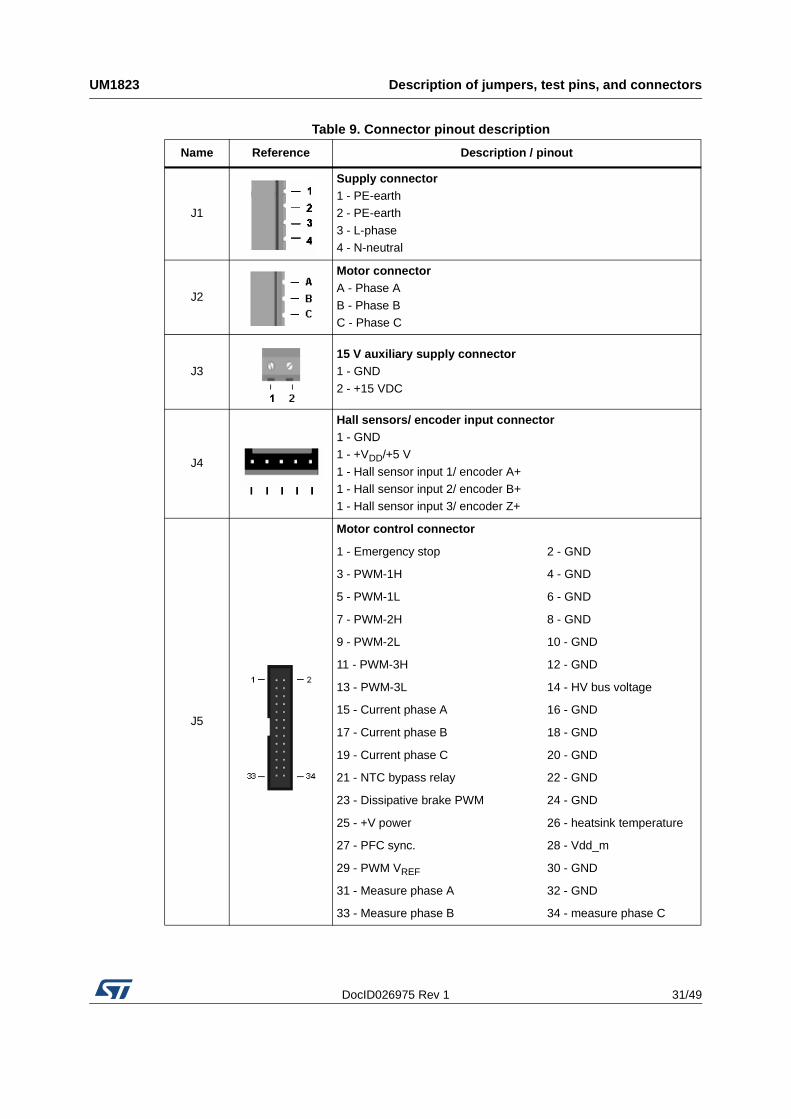
UM1823 Description of jumpers, test pins, and connectors
49
Table 9. Connector pinout description
Name Reference Description / pinout
J1
Supply connector1 - PE-earth2 - PE-earth
3 - L-phase4 - N-neutral
J2
Motor connectorA - Phase A
B - Phase BC - Phase C
J3
15 V auxiliary supply connector1 - GND
2 - +15 VDC
J4
Hall sensors/ encoder input connector1 - GND1 - +VDD/+5 V
1 - Hall sensor input 1/ encoder A+1 - Hall sensor input 2/ encoder B+1 - Hall sensor input 3/ encoder Z+
J5
Motor control connector
1 - Emergency stop 2 - GND
3 - PWM-1H 4 - GND
5 - PWM-1L 6 - GND
7 - PWM-2H 8 - GND
9 - PWM-2L 10 - GND
11 - PWM-3H 12 - GND
13 - PWM-3L 14 - HV bus voltage
15 - Current phase A 16 - GND
17 - Current phase B 18 - GND
19 - Current phase C 20 - GND
21 - NTC bypass relay 22 - GND
23 - Dissipative brake PWM 24 - GND
25 - +V power 26 - heatsink temperature
27 - PFC sync. 28 - Vdd_m
29 - PWM VREF 30 - GND
31 - Measure phase A 32 - GND
33 - Measure phase B 34 - measure phase C
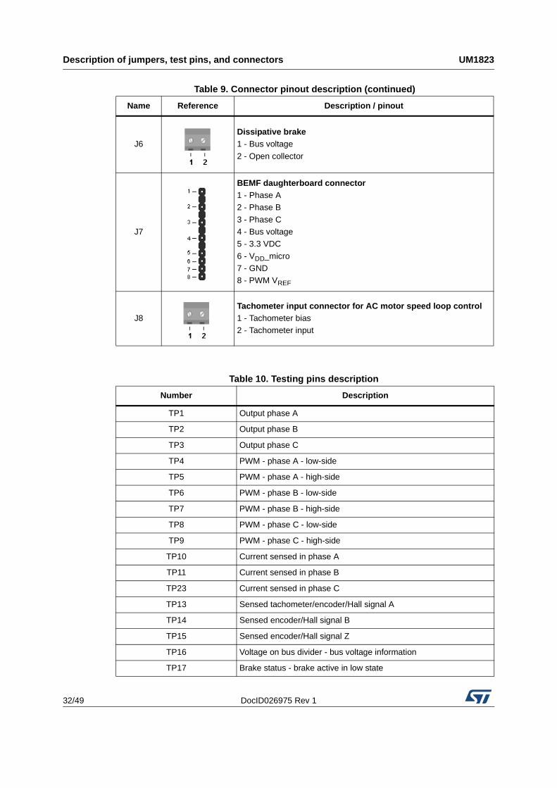
Description of jumpers, test pins, and connectors UM1823
32/49 DocID026975 Rev 1
J6
Dissipative brake1 - Bus voltage
2 - Open collector
J7
BEMF daughterboard connector1 - Phase A2 - Phase B
3 - Phase C4 - Bus voltage5 - 3.3 VDC
6 - VDD_micro7 - GND8 - PWM VREF
J8
Tachometer input connector for AC motor speed loop control1 - Tachometer bias2 - Tachometer input
Table 10. Testing pins description
Number Description
TP1 Output phase A
TP2 Output phase B
TP3 Output phase C
TP4 PWM - phase A - low-side
TP5 PWM - phase A - high-side
TP6 PWM - phase B - low-side
TP7 PWM - phase B - high-side
TP8 PWM - phase C - low-side
TP9 PWM - phase C - high-side
TP10 Current sensed in phase A
TP11 Current sensed in phase B
TP23 Current sensed in phase C
TP13 Sensed tachometer/encoder/Hall signal A
TP14 Sensed encoder/Hall signal B
TP15 Sensed encoder/Hall signal Z
TP16 Voltage on bus divider - bus voltage information
TP17 Brake status - brake active in low state
Table 9. Connector pinout description (continued)
Name Reference Description / pinout
DocID026975 Rev 1 33/49
UM1823 Connector placement
49
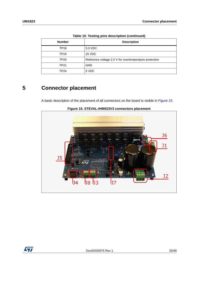
5 Connector placement
A basic description of the placement of all connectors on the board is visible in Figure 15.
Figure 15. STEVAL-IHM023V3 connectors placement
TP18 3.3 VDC
TP19 15 VDC
TP20 Reference voltage 2.5 V for overtemperature protection
TP21 GND
TP24 5 VDC
Table 10. Testing pins description (continued)
Number Description
Bill of material UM1823
34/49 DocID026975 Rev 1
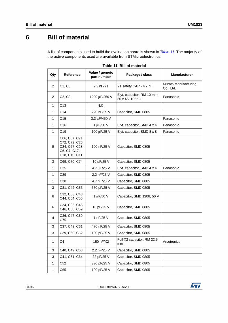
6 Bill of material
A list of components used to build the evaluation board is shown in Table 11. The majority of the active components used are available from STMicroelectronics.
Table 11. Bill of material
Qty ReferenceValue / generic
part numberPackage / class Manufacturer
2 C1, C5 2.2 nF/Y1 Y1 safety CAP - 4.7 nFMurata Manufacturing Co., Ltd.
2 C2, C3 1200 μF/250 VElyt. capacitor, RM 10 mm, 30 x 45, 105 °C
Panasonic
1 C13 N.C.
1 C14 220 nF/25 V Capacitor, SMD 0805
1 C15 3.3 μF/450 V Panasonic
1 C16 1 μF/50 V Elyt. capacitor, SMD 4 x 4 Panasonic
1 C19 100 μF/25 V Elyt. capacitor, SMD 8 x 8 Panasonic
9
C66, C67, C71, C72, C73, C26, C24, C27, C28, C6, C7, C17, C18, C10, C11
100 nF/25 V Capacitor, SMD 0805
3 C69, C70, C74 10 pF/25 V Capacitor, SMD 0805
1 C25 4.7 μF/25 V Elyt. capacitor, SMD 4 x 4 Panasonic
1 C29 2.2 nF/25 V Capacitor, SMD 0805
1 C30 4.7 nF/25 V Capacitor, SMD 0805
3 C31, C42, C53 330 pF/25 V Capacitor, SMD 0805
6C32, C33, C43, C44, C54, C55
1 μF/50 V Capacitor, SMD 1206; 50 V
6C34, C35, C45, C46, C58, C59
10 pF/25 V Capacitor, SMD 0805
4C36, C47, C60, C75
1 nF/25 V Capacitor, SMD 0805
3 C37, C48, C61 470 nF/25 V Capacitor, SMD 0805
3 C39, C50, C62 100 pF/25 V Capacitor, SMD 0805
1 C4 150 nF/X2Foil X2 capacitor, RM 22.5 mm
Arcotronics
3 C40, C49, C63 2.2 nF/25 V Capacitor, SMD 0805
3 C41, C51, C64 33 pF/25 V Capacitor, SMD 0805
1 C52 330 pF/25 V Capacitor, SMD 0805
1 C65 100 pF/25 V Capacitor, SMD 0805
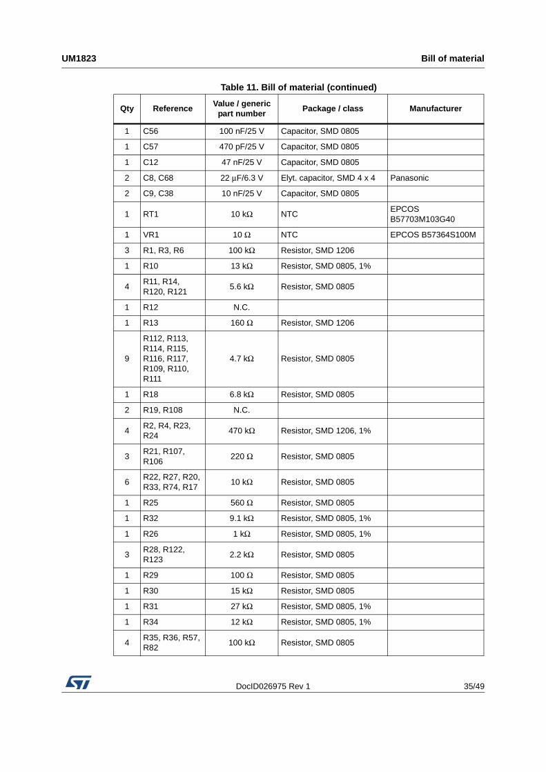
DocID026975 Rev 1 35/49
UM1823 Bill of material
49
1 C56 100 nF/25 V Capacitor, SMD 0805
1 C57 470 pF/25 V Capacitor, SMD 0805
1 C12 47 nF/25 V Capacitor, SMD 0805
2 C8, C68 22 μF/6.3 V Elyt. capacitor, SMD 4 x 4 Panasonic
2 C9, C38 10 nF/25 V Capacitor, SMD 0805
1 RT1 10 kΩ NTCEPCOS B57703M103G40
1 VR1 10 Ω NTC EPCOS B57364S100M
3 R1, R3, R6 100 kΩ Resistor, SMD 1206
1 R10 13 kΩ Resistor, SMD 0805, 1%
4R11, R14, R120, R121
5.6 kΩ Resistor, SMD 0805
1 R12 N.C.
1 R13 160 Ω Resistor, SMD 1206
9
R112, R113, R114, R115, R116, R117, R109, R110, R111
4.7 kΩ Resistor, SMD 0805
1 R18 6.8 kΩ Resistor, SMD 0805
2 R19, R108 N.C.
4R2, R4, R23, R24
470 kΩ Resistor, SMD 1206, 1%
3R21, R107, R106
220 Ω Resistor, SMD 0805
6R22, R27, R20, R33, R74, R17
10 kΩ Resistor, SMD 0805
1 R25 560 Ω Resistor, SMD 0805
1 R32 9.1 kΩ Resistor, SMD 0805, 1%
1 R26 1 kΩ Resistor, SMD 0805, 1%
3R28, R122, R123
2.2 kΩ Resistor, SMD 0805
1 R29 100 Ω Resistor, SMD 0805
1 R30 15 kΩ Resistor, SMD 0805
1 R31 27 kΩ Resistor, SMD 0805, 1%
1 R34 12 kΩ Resistor, SMD 0805, 1%
4R35, R36, R57, R82
100 kΩ Resistor, SMD 0805
Table 11. Bill of material (continued)
Qty ReferenceValue / generic
part numberPackage / class Manufacturer
Bill of material UM1823
36/49 DocID026975 Rev 1
4R37, R41, R58, R62
10 Ω Resistor, SMD 0805
6R38, R59, R85, R40, R61, R87
1 kΩ Resistor, SMD 0805, 1%
4R39, R45, R60, R65
120 Ω Resistor, SMD 0805
3 R42, R63, R89 3.3 kΩ Resistor, SMD 0805
3 R43, R64, R90 47 kΩ Resistor, SMD 0805, 1%
1 R44 3.6 kΩ Resistor, SMD 0805, 1%
3 R46, R66, R92 3.3 kΩ Resistor, SMD 0805, 1%
1 R49 N.C.
2 R5, R9 120 Ω Resistor, SMD 0805
3 R52, R97, R78 3.3 kΩ Resistor, SMD 0805, 1%
3 R54, R76, R100 820 Ω Resistor, SMD 0805, 1%
3 R55, R71, R101 0.15 Ω Resistor, SMD 2512, 1%, 2 W
3 R56, R68, R102 N.C.
6R67, R70, R75, R79, R50, R53
1 kΩ Resistor, SMD 0805, 1%
1 R69 680 Ω Resistor, SMD 0805, 1%
1 R7 7.5 Ω Resistor, SMD 0805, 1%
6R72, R48, R47, R77, R51, R98
1 kΩ Resistor, SMD 0805, 1%
1 R73 N.C.
1 R8 51 kΩ Resistor, SMD 0805, 1%
1 R80 2.2 kΩ Resistor, SMD 0805, 1%
1 R81 33 Ω Resistor, SMD 0805, 1%
2 R83, R88 10 Ω Resistor, SMD 0805
1 R104 68 kΩ Resistor, SMD 0805
1 R84 2.2 kΩ Resistor, SMD 0805
2 R86, R91 120 Ω Resistor, SMD 0805
5R93, R95, R99, R94, R103
1 kΩ Resistor, SMD 0805, 1%
1 R96 N.C.
1 R105 220 kΩ Resistor, SMD 0805, 1%
1 L1 47 μH SMD choke, 0.5 A Panasonic
1 L2 2.2 mH SMD choke, 0.25 A Würth Elektronik
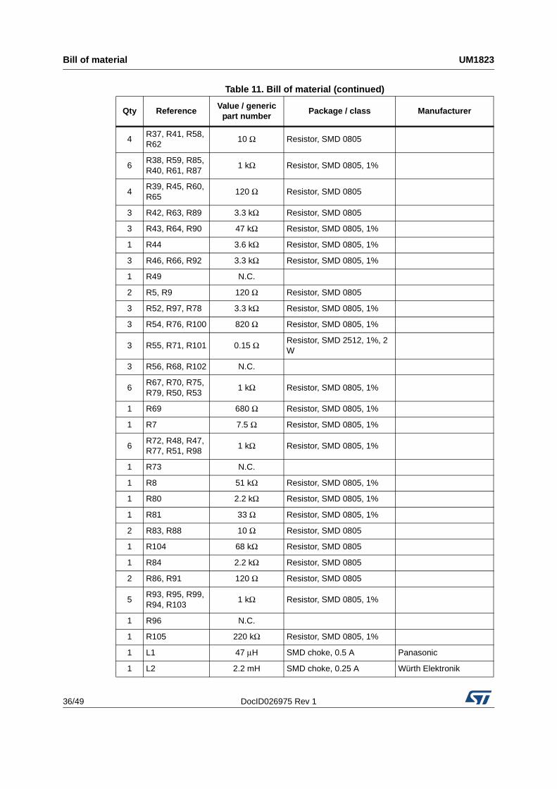
Table 11. Bill of material (continued)
Qty ReferenceValue / generic
part numberPackage / class Manufacturer
DocID026975 Rev 1 37/49
UM1823 Bill of material
49
1 D1 KBU6K Diode bridge, 250 VAC, 8 A
7D11, D12, D15, D16, D19, D20, D2, D23, D24
BAT48 Diode, SMD, SOD-323 STMicroelectronics
8D13, D5, D14, D17, D18, D21, D22, D10
1N4148Universal diode, SMD, SOD80C
2 D25, D29 BZX84B13V Zener diode, SOT23, 13 V
1 D3 STPS1150Schottky diode, DO-241AC (SMA)
STMicroelectronics
1 D4 SM6T36Transil™, JEDEC DO-214AA
STMicroelectronics
2 D6, D8 STTH1L06 HV diode, SMA STMicroelectronics
1 D7 LED GREEN Universal LED 3 mm, 2 mA
1 D9 BZV55C18SMD Zener diode, SOD80, 18 V
1 D27 LED YELLOW Universal LED 3 mm, 2 mA
1 D28 LED RED Universal LED 3 mm, 2 mA
1 D26 STTH2L06 HV diode, SMA STMicroelectronics
10
Q1, Q4, Q5, Q12, Q13, Q14, Q15, Q16, Q17, Q18
BC847 NPN transistor, SOT23
7Q10, Q11, Q3, Q6, Q7, Q8, Q9
STGP10H60DF N-channel IGBT, TO220 STMicroelectronics
1 Q2 BC857B PNP transistor, SOT23
1 F1 HolderFuse holder 5 x 20 mm, KS21 SW
SCHURTER
1 F1 6.25 AFuse 6.25 A Slov., FST06.3, 5 x 20 mm
1 LS1 Finder 4031-12 Relay 12 VDC Finder
1 U1 LD1117S33Linear regulator 3.3 V, SOT223
STMicroelectronics
1 U2 L7815Linear regulator 15 V, TO-220
STMicroelectronics
1 U3 VIPer16 Smart PWM driver, SO-16 STMicroelectronics
2 U4, U8 TS391Voltage comparator, SOT23-5
STMicroelectronics
3 U5, U6, U7 L6390HV low and high-side driver, SO-16
STMicroelectronics
Table 11. Bill of material (continued)
Qty ReferenceValue / generic
part numberPackage / class Manufacturer
Bill of material UM1823
38/49 DocID026975 Rev 1
1 U9 TS3431Voltage reference, SOT23-3L
STMicroelectronics
1 U10 L78M05C Linear regulator 5 V, DPAK STMicroelectronics
1 U11 M74HC14 Hex Schmitt inverter SOP STMicroelectronics
3 TP1, TP2, TP3 N.C.
18 TP4 - TP24PCB terminal
1 mmTest pin
1 J1 Connector 4PConnector RM 5 mm, 4-pole male horizontal
PHOENIX CONTACT
1 Connector 4PConnector RM 5 mm, 4-pole female parallel
PHOENIX CONTACT
1 J2 Connector 3PConnector RM 5 mm, 3-pole male horizontal
PHOENIX CONTACT
1 Connector 3PConnector RM 5 mm, 3-pole female parallel
PHOENIX CONTACT
1 J3 Con. 5 mm, 2PConnector RM 5 mm, 2-pole, screw
PHOENIX CONTACT
1 J4 Connector 5P Autocom HE14 5-pin Stelvio Kontek
1 J5 MLW34G MLW connector 34-pin Tyco Electronics
1 J6 Con. 5 mm, 2PConnector RM 5 mm, 2-pole, screw
PHOENIX CONTACT
1 J7Con. 2.54 mm
12-pinPins RM 2.54 mm female, 12-pin
1 J8 Con. 5 mm, 2PConnector RM 5 mm, 2-pole, screw
PHOENIX CONTACT
1 W1 Jumper 2.54Three pins of break way + jumper in position 3.3 V
1 W10 Jumper 2.54Two pins of break way + jumper
1 W11 Jumper 2.54Three pins of break way + jumper in position 3.3 V
3 W13 Mounting holeThree way HV selector, default three-shunt position
1Insulated jumper
blue
HV insulated jumper, 5.08 mm, default three-shunt position
3 W3 Mounting hole Three way HV selector
1Insulated jumper
blue
HV insulated jumper, 5.08 mm, default “HIGH VOLTAGE” position
Table 11. Bill of material (continued)
Qty ReferenceValue / generic
part numberPackage / class Manufacturer

DocID026975 Rev 1 39/49
UM1823 Bill of material
49
1 W4 Jumper 2.54Two pins of break way + jumper
1 W5 Jumper 2.54Three pins of break way + jumper in position R_BRAKE
1 W6 Jumper 2.54 Two pins of break way
1 W7 Jumper 2.54 Two pins of break way
3 W9 Mounting holeThree way HV selector, default three-shunt position
1Insulated jumper
blue
HV insulated jumper, 5.08 mm, default three-shunt position
1 W14 Wire jumper Not assembled
1 W16 Jumper 2.54Three pins of break way + jumper in position 1
150 mm
Het 1 Heatsink 150 mm of AL profile 8693 PADA Engineering
1 Het 2 HeatsinkHeatsink for TO-220 with montage pin
PADA Engineering
7 Clip for hetMontage clip PADA 7704, TO-220, 10 mm
PADA Engineering
1 Clip for hetMontage clip PADA 7703, TO-220, 15 mm
PADA Engineering
130 mm
Isolation tapeIsolation tape, 24 mm wide; approx. 130 mm long, self adhesive
Table 11. Bill of material (continued)
Qty ReferenceValue / generic
part numberPackage / class Manufacturer

PCB layout UM1823
40/49 DocID026975 Rev 1
7 PCB layout
For this application a standard, double-layer, coppered PCB with a ~60 μm copper thickness was selected. The PCB material is FR-4.
The dimensions of the board are:
Length: 182 mm
Width: 127 mm
PCB thickness: 1.55 mm
DocID026975 Rev 1 41/49
UM1823 PCB layout
49
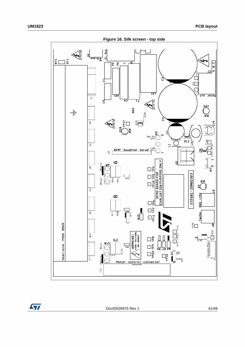
Figure 16. Silk screen - top side
PCB layout UM1823
42/49 DocID026975 Rev 1
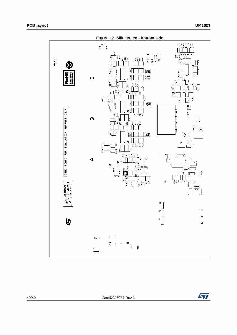
Figure 17. Silk screen - bottom side

DocID026975 Rev 1 43/49
UM1823 PCB layout
49
Figure 18. Copper tracks - top side
Figure 19. Copper tracks - bottom side

Ordering information UM1823
44/49 DocID026975 Rev 1
8 Ordering information
The evaluation board is orderable through the standard ordering system, the ordering code is: STEVAL-IHM023V3. The items delivered include the assembled evaluation board, board documentation, PCB fabrication data such as gerber files, assembly files (pick and place), and component documentation.
9 Using STEVAL-IHM023V3 with STM32 PMSM FOC SDK
The “STM32 PMSM FOC firmware library” is part of the STM32 PMSM single/dual FOC SDK. In particular, it is a firmware library running on any STM32F103x and STM32F100x device which implements the “Field Oriented Control” (FOC) drive of three-phase “Permanent Magnet Synchronous Motors” (PMSM), both “Surface Mounted” (SM-PMSM) and “Internal” (I-PMSM).
This section describes how to customize the firmware library by making use of the PC tool “ST MC Workbench” downloadable from www.st.com.
9.1 Environmental considerations
Warning: The STEVAL-IHM023V3 evaluation board must only be used in a power laboratory. The voltage used in the drive system presents a shock hazard.
The kit is not electrically isolated from the DC input. This topology is very common in motor drives. The microprocessor is grounded by the integrated ground of the DC bus. The microprocessor and associated circuitry are hot and MUST be isolated from user controls and communication interfaces.
Warning: All measuring equipment must be isolated from the main power supply before powering up the motor drive. To use an oscilloscope with the kit, it is safer to isolate the DC supply AND the oscilloscope. This prevents a shock occurring as a result of touching any SINGLE point in the circuit, but does NOT prevent shocks when touching two or more points in the circuit.
An isolated AC power supply can be constructed using an isolation transformer and a variable transformer.
Note: Isolating the application rather than the oscilloscope is highly recommended in any case.
DocID026975 Rev 1 45/49
UM1823 Using STEVAL-IHM023V3 with STM32 PMSM FOC SDK
49
9.2 Hardware requirementsThe following items are required to run the STEVAL-IHM023V3 together with the “STM32 PMSM FOC firmware library v3.4”.
• Any microcontroller evaluation board with MC connector
• A high-voltage insulated AC power supply up to 230 VAC
• A programmer/debugger dongle for control board (not included in the package). Refer to the control board user manual to find a supported dongle. Use of an insulated dongle is always recommended.
• Three-phase brushless motor with permanent magnet rotor (not included in the package)
• An insulated oscilloscope (as necessary)
• An insulated multimeter (as necessary)
9.3 Software requirementsTo customize, compile, and download the “STM32 FOC firmware library”, a toolchain must be installed.
9.4 STM32 FOC firmware library customizationThe ST motor control workbench can be used to customize the STM32 FOC firmware library.
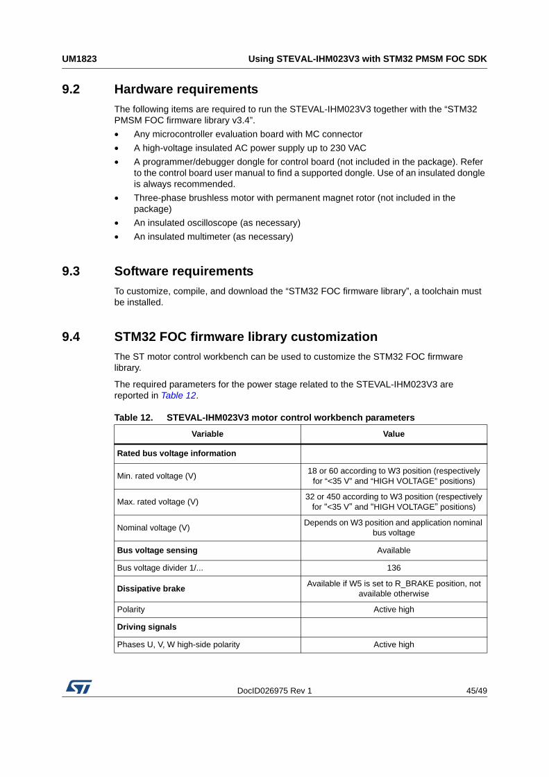
The required parameters for the power stage related to the STEVAL-IHM023V3 are reported in Table 12.
Table 12. STEVAL-IHM023V3 motor control workbench parameters
Variable Value
Rated bus voltage information
Min. rated voltage (V)18 or 60 according to W3 position (respectively
for “<35 V” and “HIGH VOLTAGE” positions)
Max. rated voltage (V)32 or 450 according to W3 position (respectively
for “<35 V” and “HIGH VOLTAGE” positions)
Nominal voltage (V)Depends on W3 position and application nominal
bus voltage
Bus voltage sensing Available
Bus voltage divider 1/... 136
Dissipative brakeAvailable if W5 is set to R_BRAKE position, not
available otherwise
Polarity Active high
Driving signals
Phases U, V, W high-side polarity Active high
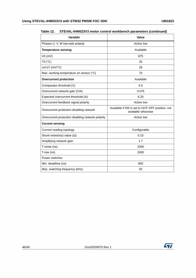
Using STEVAL-IHM023V3 with STM32 PMSM FOC SDK UM1823
46/49 DocID026975 Rev 1
Phases U, V, W low-side polarity Active low
Temperature sensing Available
V0 (mV) 875
T0 (°C) 25
ΔV/ΔT (mV/°C) 28
Max. working temperature on sensor (°C) 70
Overcurrent protection Available
Comparator threshold (V) 0.5
Overcurrent network gain (V/A) 0.075
Expected overcurrent threshold (A) 6.25
Overcurrent feedback signal polarity Active low
Overcurrent protection disabling networkAvailable if W5 is set to OCP OFF position, not
available otherwise
Overcurrent protection disabling network polarity Active low
Current sensing
Current reading topology Configurable
Shunt resistor(s) value (Ω) 0.15
Amplifying network gain 1.7
T-noise (ns) 2000
T-rise (ns) 2000
Power switches
Min. deadtime (ns) 800
Max. switching frequency (kHz) 50
Table 12. STEVAL-IHM023V3 motor control workbench parameters (continued)
Variable Value
DocID026975 Rev 1 47/49
UM1823 Conclusion
49
10 Conclusion
This document describes the 1 kW three-phase motor control STEVAL-IHM023V3 evaluation board as a universal fully evaluated and adaptable motor control platform.
11 References
1. L6390 datasheet
2. VIPer16 datasheet
3. STGP10H60DF datasheet
4. UM0379 user manual
5. UM0580 user manual

Revision history UM1823
48/49 DocID026975 Rev 1
12 Revision history
Table 13. Document revision history
Date Revision Changes
03-Dec-2014 1 Initial release.

DocID026975 Rev 1 49/49
UM1823
49
IMPORTANT NOTICE – PLEASE READ CAREFULLY
STMicroelectronics NV and its subsidiaries (“ST”) reserve the right to make changes, corrections, enhancements, modifications, and improvements to ST products and/or to this document at any time without notice. Purchasers should obtain the latest relevant information on ST products before placing orders. ST products are sold pursuant to ST’s terms and conditions of sale in place at the time of order acknowledgement.
Purchasers are solely responsible for the choice, selection, and use of ST products and ST assumes no liability for application assistance or the design of Purchasers’ products.
No license, express or implied, to any intellectual property right is granted by ST herein.
Resale of ST products with provisions different from the information set forth herein shall void any warranty granted by ST for such product.
ST and the ST logo are trademarks of ST. All other product or service names are the property of their respective owners.
Information in this document supersedes and replaces information previously supplied in any prior versions of this document.
© 2014 STMicroelectronics – All rights reserved