Embed Size (px)
Citation preview

1HPEC 9/22/09
Peter M. KoggeMcCourtney Chair in Computer Science & Engineering
Univ. of Notre DameIBM Fellow (retired)
May 5, 2009
TeraFlop Embedded
PetaFlop Departmental
ExaFlop Data Center
Exascale Computing:Embedded Style

2HPEC 9/22/09
Thesis
• Last 30 years: “Gigascale” computing first in a single vector processor “Terascale” computing first via several thousand microprocessors “Petascale” computing first via several hundred thousand cores
• Commercial technology: to date Always shrunk prior “XXX” scale to smaller form factor Shrink, with speedup, enabled next “XXX” scale
• Space/Embedded computing has lagged far behind Environment forced implementation constraints Power budget limited both clock rate & parallelism
• “Exascale” now on horizon But beginning to suffer similar constraints as space And technologies to tackle exa challenges very relevant
Especially Energy/Power

3HPEC 9/22/09
Topics
• The DARPA Exascale Technology Study• The 3 Strawmen Designs• A Deep Dive into Operand Access

4HPEC 9/22/09
Disclaimers
This presentation reflects my interpretation of the final report of the Exascale working group only, and not necessarily of the universities, corporations, or other institutions to which the members are affiliated.
Furthermore, the material in this document does not reflect the official views, ideas, opinions and/or findings of DARPA, the Department of Defense, or of the United States government.
http://www.cse.nd.edu/Reports/2008/TR-2008-13.pdf
Note: Separate Exa Studies on Resiliency & Software

5HPEC 9/22/09
11 Academic 6 Non-Academic 5 “Government”+ Special Domain Experts
11 Academic 6 Non-Academic 5 “Government”+ Special Domain Experts
The Exascale Study Group
UT-AustinSteve KecklerColumbiaKeren Bergman
AffiliationNAMEAffiliationNAME
MicronDean KleinIntelShekhar Borkar
Notre DamePeter KoggeGTRIDan Campbell
UC-BerkeleyKathy YelickSTASherman Karp
HPStan WilliamsSTAJon Hiller
LSUThomas SterlingAFRLKerry Hill
SDSCAllan SnavelyDARPABill Harrod
CraySteve ScottNCSUPaul Franzon
AFRLAl ScarpeliIBMMonty Denneau
Georgia TechMark RichardsStanfordBill Dally
USC/ISIBob LucasIDABill Carlson
10+ Study Meetings over 2nd half 200710+ Study Meetings over 2nd half 2007

6HPEC 9/22/09
The DARPA Exascale Technology Study
• Exascale = 1,000X capability of Petascale• Exascale != Exaflops but
Exascale at the data center size => Exaflops Exascale at the “rack” size => Petaflops for
departmental systems Exascale embedded => Teraflops in a cube
• Teraflops to Petaflops took 14+ years 1st Petaflops workshop: 1994 Thru NSF studies, HTMT, HPCS … To give us to Peta now
• Study Questions: Can we ride silicon to Exa By 2015? What will such systems look like?
• Can we get 1 EF in 20 MW & 500 racks?
Where are the Challenges?

7HPEC 9/22/09
The Study’s Approach
• Baseline today’s: Commodity Technology Architectures Performance (Linpack)
• Articulate scaling of potential application classes• Extrapolate roadmaps for
“Mainstream” technologies Possible offshoots of mainstream technologies Alternative and emerging technologies
• Use technology roadmaps to extrapolate use in “strawman” designs• Analyze results & Id “Challenges”

8HPEC 9/22/09
Context: Focus on Energy
Not Power

9HPEC 9/22/09
CMOS Energy 101
Vin Vg
R & C C
0
0.2
0.4
0.6
0.8
1
1.2
0 5 10 15 20V
olt
age
Vin
Vg
Dissipate CV2/2And store CV2/2
Dissipate CV2/2From Capacitance
One clock cycle dissipates C*V2

10HPEC 9/22/09
ITRS Projections
10
100
1000
1985 1990 1995 2000 2005 2010 2015 2020 2025
Fea
ture
Siz
e
Assume capacitance of a circuit scales as feature size
0.01
0.10
1.00
10.00
100.00
1000.00
1/1/
88
1/1/
90
1/1/
92
1/1/
94
1/1/
96
1/1/
98
1/1/
00
1/1/
02
1/1/
04
1/1/
06
1/1/
08
1/1/
10
1/1/
12
1/1/
14
1/1/
16
1/1/
18
1/1/
20
1/1/
22
1/1/
24
CV
^2 r
elat
ive
to 9
0nm
Hi P
erf
Lo
gic
High Perf Logic Low Operating Pow er Logic Memory Process
330X
15X
0
0.2
0.4
0.6
0.8
1
1.2
1.4
1.6
1.8
2
2004
2006
2008
2010
2012
2014
2016
2018
2020
2022
2024
Pro
ject
ed V
dd
High Performance Low Operating Power
Mainstream DRAM Core Exascale projections
90nm picked as breakpoint because that’s when Vdd and thus clocks flattened

11HPEC 9/22/09
Energy Efficiency
1.E+00
1.E+01
1.E+02
1.E+03
1.E+04
1.E+05
1.E+06
1.E+07
1.E+08
1.E+09
1.E+10
1/1/80 1/1/84 1/1/88 1/1/92 1/1/96 1/1/00 1/1/04 1/1/08 1/1/12 1/1/16 1/1/20
En
erg
y p
er F
lop
( p
J/F
lop
)
Historical Top 10
Green 500 Top 10 UHPC Cabinent Goal
UHPC Cabinent Energy Efficiency Goal UHPC Module Energy Efficiency Goal
Exa Simplistically Scaled Projection Exa Fully Scaled Projection
Top System Trend Line CMOS Technology

12HPEC 9/22/09
The 3 Study Strawmen

13HPEC 9/22/09
Architectures Considered
•Evolutionary Strawmen “Heavyweight” Strawman based on
commodity-derived microprocessors “Lightweight” Strawman based on custom
microprocessors
•Aggressive Strawman
“Clean Sheet of Paper” CMOS Silicon

14HPEC 9/22/09
A Modern HPC System
Power Distribution
Memory9%
Routers33%
Random2%
Processors56%
Silicon Area Distribution
Processors3%
Routers3%
Memory86%
Random8%
Board Area Distribution
Memory10%
Processors24%
Routers8%
White Space50%
Random8%

15HPEC 9/22/09
A “Light Weight” Node Alternative
2 Nodes per “Compute Card.” Each node:• A low power compute chip• Some memory chips• “Nothing Else”
System Architecture:• Multiple Identical Boards/Rack• Each board holds multiple Compute Cards• “Nothing Else”
• 2 simple dual issue cores• Each with dual FPUs• Memory controller• Large eDRAM L3• 3D message interface• Collective interface• All at subGHz clock“Packaging the Blue Gene/L supercomputer,” IBM J. R&D, March/May 2005
“Blue Gene/L compute chip: Synthesis, timing, and physical design,” IBM J. R&D, March/May 2005

16HPEC 9/22/09
Possible System Power Models:Interconnect Driven
• Simplistic: A highly optimistic modelMax power per die grows as per ITRSPower for memory grows only linearly with # of chips
• Power per memory chip remains constantPower for routers and common logic remains constant
• Regardless of obvious need to increase bandwidthTrue if energy for bit moved/accessed decreases as fast as “flops per
second” increase
• Fully Scaled: A pessimistic modelSame as Simplistic, except memory & router power grow with peak
flops per chipTrue if energy for bit moved/accessed remains constant
• Real world: somewhere in between

17HPEC 9/22/09
1 EFlop/s “Clean Sheet of Paper” Strawman
• 4 FPUs+RegFiles/Core (=6 GF @1.5GHz)• 1 Chip = 742 Cores (=4.5TF/s)
• 213MB of L1I&D; 93MB of L2• 1 Node = 1 Proc Chip + 16 DRAMs (16GB)• 1 Group = 12 Nodes + 12 Routers (=54TF/s)• 1 Rack = 32 Groups (=1.7 PF/s)
• 384 nodes / rack• 3.6EB of Disk Storage included • 1 System = 583 Racks (=1 EF/s)
• 166 MILLION cores• 680 MILLION FPUs• 3.6PB = 0.0036 bytes/flops• 68 MW w’aggressive assumptions
Sizing done by “balancing” power budgets with achievable capabilities
Largely due to Bill Dally, Stanford

18HPEC 9/22/09
A Single Node (No Router)
(a) Quilt Packaging (b) Thru via chip stack
Reg File11%
Cache Access20%
Off-chip13%
Leakage28%
On-chip 6% DRAM Access
1%
FPU21%
NodePower
Characteristics:• 742 Cores; 4 FPUs/core • 16 GB DRAM• 290 Watts• 1.08 TF Peak @ 1.5GHz• ~3000 Flops per cycle
“Stacked” Memory

19HPEC 9/22/09
1 Eflops Aggressive Strawman Data Center Power Distribution
Processor13%
Router34%
DRAM3%
Network50%
FPU16%
Memory29%
Interconnect29%
Leakage26%
Reg File28%
L139%
L2/L316%
DRAM3%
Disk14%
(a) Overall System Power (b) Memory Power (c) Interconnect Power
Processor13%
Router34%
DRAM3%
Network50%
FPU16%
Memory29%
Interconnect29%
Leakage26%
Reg File28%
L139%
L2/L316%
DRAM3%
Disk14%
(a) Overall System Power (b) Memory Power (c) Interconnect Power
• 12 nodes per group• 32 groups per rack• 583 racks• 1 EFlops/3.6 PB• 166 million cores• 67 MWatts

20HPEC 9/22/09
Data Center Performance Projections
1.E+04
1.E+05
1.E+06
1.E+07
1.E+08
1.E+09
1.E+10
1/1/04 1/1/08 1/1/12 1/1/16 1/1/20
GF
lop
s
Exascale
But not at 20 MW!
Heavyweight
Lightweight
21HPEC 9/22/09
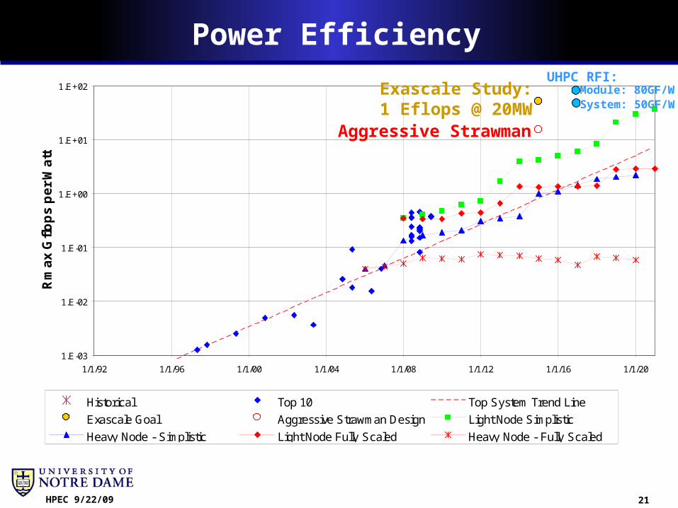
Power Efficiency
1.E-03
1.E-02
1.E-01
1.E+00
1.E+01
1.E+02
1/1/92 1/1/96 1/1/00 1/1/04 1/1/08 1/1/12 1/1/16 1/1/20
Rm
ax
Gfl
op
s p
er
Wa
tt
Historical Top 10 Top System Trend Line
Exascale Goal Aggressive Strawman Design Light Node Simplistic
Heavy Node - Simplistic Light Node Fully Scaled Heavy Node - Fully Scaled
Exascale Study:1 Eflops @ 20MW
UHPC RFI:Module: 80GF/WSystem: 50GF/W
Aggressive Strawman

22HPEC 9/22/09
Energy Efficiency
1.E+00
1.E+01
1.E+02
1.E+03
1.E+04
1.E+05
1.E+06
1.E+07
1.E+08
1.E+09
1.E+10
1/1/80 1/1/84 1/1/88 1/1/92 1/1/96 1/1/00 1/1/04 1/1/08 1/1/12 1/1/16 1/1/20
En
erg
y p
er F
lop
( p
J/F
lop
)
Historical Top 10
Green 500 Top 10 UHPC Cabinent Goal
UHPC Cabinent Energy Efficiency Goal UHPC Module Energy Efficiency Goal
Exa Simplistically Scaled Projection Exa Fully Scaled Projection
Top System Trend Line CMOS Technology

23HPEC 9/22/09
1.E+03
1.E+04
1.E+05
1.E+06
1.E+07
1.E+08
1.E+09
1.E+10
1/1/96 1/1/00 1/1/04 1/1/08 1/1/12 1/1/16 1/1/20
To
tal
Co
ncu
rrec
ncy
Top 10 Top System Top 1 Trend
Historical Exa Strawman Evolutionary Light Node
Evolutionary Heavy Node
Data Center Total Concurrency
Billion-way concurrency
Million-way concurrency
Thousand-way concurrency

24HPEC 9/22/09
Data Center Core Parallelism
1.E+02
1.E+03
1.E+04
1.E+05
1.E+06
1.E+07
1.E+08
1.E+09
1/1/96 1/1/00 1/1/04 1/1/08 1/1/12 1/1/16 1/1/20
Pro
cess
or
Par
alle
lism
Historical Top 10 Top System
Exa Strawman Evolutionary Light Node Evolutionary Heavy Node
170 Million Cores
AND we will need10-100X moreThreading forLatency Management

25HPEC 9/22/09
Key Take-Aways
• Developing Exascale systems really tough In any time frame, for any of the 3 classes
• Evolutionary Progression is at best 2020ishWith limited memory
• 4 key challenge areas Power:Concurrency: Memory CapacityResiliency
• Requires coordinated, cross-disciplinary efforts

26HPEC 9/22/09
Embedded Exa:A Deep Dive into
Interconnectto Deliver Operands

27HPEC 9/22/09
Tapers
• Bandwidth Taper: How effective bandwidth of operands being sent to a functional unit varies with location of the operands in memory hierarchy. Units: Gbytes/sec, bytes/clock, operands per flop time
• Energy Taper: How energy cost of transporting operands to a functional unit varies with location of the operands in the memory hierarchy. Units: Gbytes/Joule, operands per Joule
• Ideal tapers: “Flat”–doesn’t matter where operands are.
• Real tapers: huge dropoffs

28HPEC 9/22/09
An Exa Single Node for Embedded
(a) Quilt Packaging (b) Thru via chip stack
Reg File11%
Cache Access20%
Off-chip13%
Leakage28%
On-chip 6% DRAM Access
1%
FPU21%

29HPEC 9/22/09
The Access Path: Interconnect-Driven
ROUTER
MemoryMICROPROCESSOR
MoreRouters
Some sort of memory structure

30HPEC 9/22/09
Sample Path – Off Module Access
1. Check local L1 (miss)2. Go thru TLB to remote L3 (miss)3. Across chip to correct port (thru routing table RAM)4. Off-chip to router chip5. 3 times thru router and out6. Across microprocessor chip to correct DRAM I/F7. Off-chip to get to correct DRAM chip8. Cross DRAM chip to correct array block9. Access DRAM Array10. Return data to correct I/R11. Off-cchip to return data to microprocessor12. Across chip to Routre Table13. Across microprocessor to correct I/O port 14. Off-chip to correct router chip15. 3 times thru router and out16. Across microprocessor to correct core17. Save in L2, L1 as required18. Into Register File

31HPEC 9/22/09
Taper Data from Exascale Report

32HPEC 9/22/09
Bandwidth Tapers
0.001
0.01
0.1
1
10
RF L1 L2 L3 LD ND
Memory Structure
Ban
dw
idth
: O
per
and
s/fl
op
0.001
0.01
0.1
1
10
1.E+03 1.E+05 1.E+07 1.E+09 1.E+11 1.E+13 1.E+15 1.E+17
Memory Capacity (B)
Ban
dw
idth
: O
per
and
s/fl
op
1,000X Decrease Across the System!!

33HPEC 9/22/09
Energy Analysis: Possible Storage Components
0.001
0.01
0.1
1
10
2004 2006 2008 2010 2012 2014 2016 2018 2020 2022 2024
Op
eran
ds/
pJ
RF: LOP; 4P; 1x128W RF: HP; 4P; 1x128W
32KB RAM: HP; 1P, 1x4KW 32KB Cache: LOP; 1P, DM; 1W Block
32KB RAM: LOP; 1P, 1x4KW 32KB RAM: LP-DRAM; 1P, 1x4KW
32KB Cache: LOP; 1P, DM; 4W Block 1M RAM: LOP, 1P, 1 Bank
1M RAM: LP-DRAM, 1P, 8 Bank 1M RAM: Comm-DRAM, 1P, 1 Bank
RF from Exa Study 32KB SRAM Exa Study
DRAM from Exa Study
Cacti 5.3
Extrapolation
Technology for 2017 system

34HPEC 9/22/09
Summary Transport Options
1 Operand/word = 72 bits

35HPEC 9/22/09
Energy Tapers vs GoalsReachable Opernads
Path Capacity(MB) Total Transport Access %Transport per pJRegister File 9.77E-04 0.7 0.0 0.7 0.0% 1.436
L1 Hit 3.13E-02 3.9 0.0 3.9 0.0% 0.260L1 Miss, Local L2 Hit 2.50E-01 30.6 13.3 17.3 43.4% 0.033
L1 Miss, L3 Hit 3.04E+02 158.3 141.0 17.3 89.1% 0.006L1,L2/L3 Miss On-Module Access 6.55E+04 292.1 255.0 37.1 87.3% 0.003L1,L2/L3 Miss Off-Module Access 2.52E+07 6620.8 6607.2 13.7 99.8% 0.000
Energy (pJ)
0.000
0.001
0.010
0.100
1.000
10.000
Register File L1 Hit L1 Miss, Local L2Hit
L1 Miss, L3 Hit L1,L2/L3 Miss On-Module Access
L1,L2/L3 Miss Off-Module Access
Op
eran
ds
per
pJ
Taper Rack Goal System Goal Module Goal

36HPEC 9/22/09
Reachable Memory vs Energy
0
1
10
100
1000
10000
1.00
E-0
4
1.00
E-0
3
1.00
E-0
2
1.00
E-0
1
1.00
E+
00
1.00
E+
01
1.00
E+
02
1.00
E+
03
1.00
E+
04
1.00
E+
05
1.00
E+
06
1.00
E+
07
1.00
E+
08
Reachable memory (MB)
En
erg
y p
er O
per
and
(p
J)

37HPEC 9/22/09
What Does This Tell Us?
• There’s a lot more energy sinks than you think And we have to take all of them into consideration
• Cost of Interconnect Dominates• Must design for on-board or stacked DRAM, with
DRAM blocks CLOSE take into account physical placement
• Reach vs energy per access looks “linear”• For 80GF/W, cannot afford ANY memory references• We NEED to consider the entire access path:
Alternative memory technologies – reduce access cost Alternative packaging costs – reduce bit movement cost Alternative transport protocols – reduce # bits moved Alternative execution models – reduce # of movements