Embed Size (px)
Citation preview

1
Analysis of Distortion in Pulse Modulation
Converters for Switching Radio Frequency
Power Amplifiers
Vandana Bassoo, Lance Linton and Mike Faulkner
Centre for Telecommunications and Micro-Electronics,
Victoria University, Australia
E-mail: [email protected]
Abstract
High efficiency linear radio frequency (RF) power amplifiers (PAs) are needed for today’s wireless
communication systems. Switch mode techniques have the potential for high efficiency but require
a pulse drive signal. The generation of pulse width modulated signals and pulse position modulated
signals by sigma delta modulators can introduce unwanted spectral components. Third order and image
components are the dominant distortions generated in the pulse position modulation circuit. We identify
the cause of distortion and mathematically quantify its amplitude and frequency. In a single carrier
environment, an increase in offset frequency increases the unwanted spectral components. Calculations,
simulations and measurements show that offsets less than 1% of the carrier frequency are required to
keep unwanted components 40 dB below the signal level. Simulations and measurements show that the
effect on a multi-channel OFDM system is less detrimental. Nonetheless, unacceptable noise increases
of up to 20 dB are observed in odd harmonic channels when the transmission is not centered on the
nominal carrier frequency.

2
I. INTRODUCTION
A recent study estimated that by 2013, 80% of the three billion broadband users will be
connected through a wireless device [1]. This has to be achieved within the constraints of
today’s fragmented spectrum, multiple operating standards, and the need for low carbon foot-
print. Therefore, next generation transmitter architectures need to be bandwidth efficient, power
efficient, broadband and flexible. Bandwidth efficient multi-carrier schemes such as orthogonal
frequency division multiplexing (OFDM) are normally amplified using conventional linear power
amplifiers; however the efficiency is very poor. Switch mode power amplifiers (SMPAs), such
as class E amplifiers, are known to be highly efficient but non-linear. Using a pulse train as
the drive signal by-passes the linearity issue of SMPAs. The phase and amplitude information is
embedded in the edges of the pulse train. Over the years, process technology has improved and it
is possible to directly generate the digital drive signals using sigma delta (Σ∆) techniques. All-
digital modulators using bandpass or lowpass Σ∆ modulators have been proposed in [2]- [4]. Fig.
1 shows a potential candidate for the future generation wireless transmitters using Class D, E or
F SMPAs 1. The new structure requires a bandpass filter at the output but eliminates the need for
most other analog components such as digital to analog converters (DACs), reconstruction filters,
the local oscillator and the quadrature modulator. It also provides the possibility of integrating
both the digital and microwave sections on to a single chip [5].
Recent Σ∆ solutions have targeted two different problem areas, the first is the reduction of
digital processing load, which is necessary for low power operation at microwave frequencies,
and the second seeks to improve the efficiency of the SMPA by reducing the switching activity.
1Class E or F are usually preferred for high carrier frequencies because the parisitics form part of the load network or areresonated out. Class D is suitable for lower operating frequencies [6].

3
One of the earliest methods uses a fourth-order bandpass Σ∆ clocked at four times the carrier
frequency to generate the binary input drive signal for the SMPA [7]. The high clock rate means
that the Σ∆ consumes considerable digital power. Researchers in [8]- [9] replaced the bandpass
Σ∆ with a two low pass Σ∆ operating at lower clock frequencies. This reduces the Σ∆ sample
rate by two. The sample rate reduction in [9] was more aggressive leading to burst mode operation
and the digital processing load was further improved. However reducing the Σ∆ sample rate also
reduces the signal bandwidth, which was partially compensated for by increasing the effective
order of the filter. In the methods described in [8]- [9], switching activity occurs at least once per
RF period, even if the input signal is small or absent, leading to an increase in SMPA switching
activity.
Two possible techniques that reduce switching activity are the polar Σ∆ [4] and the Cartesian
Σ∆ [10]. The polar Σ∆ consists of two lowpass Σ∆s operating on polar representations of
the baseband signal, followed by an upconversion block, that performs polar to pulse width
modulation (PWM) and pulse position modulation (PPM). The Cartesian Σ∆ uses the same
upconversion block but performs the baseband Σ∆ filtering in the Cartesian domain, thus
improving the signal to quantisation noise ratio (SQNR) [10]. Both schemes limit the number
of pulses to a maximum of one pulse per period (or half period) of the RF carrier. Often there
are no switching pulses, when the input signal is small, thus reducing switching loss which
is a principal source of power loss in the amplifier. However, in [4], it was mentioned that a
number of spurious tones were observed in the output spectrum. The problem was attributed to
non-linearities in the modulation process. The authors verified this in [11].
We show that the presence of the spurious tones is due to the PPM process. The significant
contribution of this paper is the mathematical analysis which quantifies the distortion. The

4
dominant distortion products are the third harmonic and the image both of which fold in from
other harmonic zones. We validate the results by simulations and measurements. The PPM section
is responsible for the phase modulation of the carrier pulse sequence. It inserts or swallows a
clock cycle to change the carrier phase (pulse position) by one quantisation level. We show
how these quantised phase jumps generate distortion components that affect both the signal
amplitude and signal phase. The analysis is performed in a single carrier environment using a
single sideband (SSB) test signal. We also use simulation and measurement to show how the
distortion can affect a multi-carrier signal. The distortion components can dominate the noise
shaping spectrum of the Σ∆ process. We show that the problem can be reduced by increasing
the oversampling rate and minimising the signal offset frequency from the centre of the band.
Section II describes the architecture of the digital drive block and explains the Σ∆ filter and the
‘polar to PWM/PPM’ block in detail. Section III intuitively describes the distortion caused by
the PPM block. A mathematical analysis of the problem is presented in Section IV. Section V
corroborates the theory by simulations and measurements using a SSB test signal. Measurement
and simulation results are also provided for a multi-carrier signal. Section VI concludes the
work.
II. ARCHITECTURE OF DIGITAL DRIVE BLOCK
Fig. 2 shows the block diagram of the proposed Cartesian Σ∆ which consists of two second-
order lowpass Σ∆s (MOD 2) [12], amplitude and phase quantisers and a ‘polar to PWM/PPM’
block. The ‘polar to PWM/PPM’ block controls the amplitude of the RF carrier signal by the
pulse width and the phase of the RF carrier by the pulse position. These can be updated at a
maximum rate of every half cycle of the RF carrier (for the tri-state waveform) or every cycle for
the two state version. Lesser update rates are possible in which case a burst of carrier waveforms

5
is generated for each input sample. The ‘polar to PWM/PPM’ also oversamples the carrier signal
by an oversampling factor, OSR.
A. Sigma Delta Filtering
Synchronous digital circuits mandate the alignment of pulse positions and pulse widths with
digital clock edges resulting in the generation of time-based quantisation noise. Σ∆ techniques
use oversampling and noise shaping to reduce the noise in the signal band. The noise shaping
is determined by the MOD-2 noise transfer function (NTF) which provides increased noise
attenuation for frequencies close to DC. The signal transfer function is unity and the NTF is
given by
NTF = (1− z−1)2 (1)
In operation, the Cartesian signals pass through the Σ∆ filters, after which they are converted
to polar [R, θ] for quantisation in blocks QR and Qθ (Fig. 2). The quantised signals [R, θ] are
then reconverted to Cartesian before being fed back to the filters [10].
B. Polar to PWM/PPM
The ‘polar to PWM/PPM’ block is responsible for upconverting the filtered and quantised
polar signals to RF using PPM and PWM. The location of the pulse is determined using the
quantised phase, θ. The phase modulated signal is then fed to a pulse width modulator where
the quantised amplitude, R is converted to duration as in [4]. The equations from [13] are used
to decide the amplitude quantisation levels for the polar quantiser. In this case, the amplitude is
quantised into (OSR2
+1) levels corresponding to pulse widths of (0, 2OSR
, 4OSR
, 6OSR
. . . OSR/2OSR
) 1fc
(fc = carrier frequency). The phase is quantised into OSR phase increments from zero to 2π.

6
This quantisation process requires the system digital clock to oversample fc by a factor of OSR
therefore fclk = OSRfc. The pulse edges are confined to the sampling grid with OSR samples
per period.
III. PHASE MODULATION TO AMPLITUDE MODULATION DISTORTION
The phase modulation operates by swallowing or stuffing a pulse whenever θ moves from one
phase quantisation level to another. The loss or gain of a pulse affects the mark-space ratio which
represents the amplitude of the signal. It can thus be deduced that phase modulation (PM) leads
to amplitude modulation (AM) distortion. The distortion is more significant when a ‘high’ pulse
is affected. The phenomenon manifests itself in the spectral domain as images and harmonic
components when the baseband input signal is a phase ramp or SSB tone in the RF domain.
Fig. 3 shows the pulse extension effect. For illustrative purposes, the repeating pulse train is
divided into sections of two periods. Waveform (a) shows the original reference waveform at
fc. At the second period of waveform (b), there is a change in phase. The change in phase is
represented by a change in position. In the remaining waveforms, the phase is incremented at
every second period to produce a SSB signal at fc + fssb. A change in phase causes a change in
the mark-space ratio between two consecutive pulses. At some stage, the high pulses will join
to form a wider high pulse (waveform(i)). The amplitude is no longer one pulsewidth wide.
Since the ‘polar to PWM/PPM’ block is located outside the Σ∆ loop, the error cannot be
corrected by the feedback mechanism. The situation is undesirable since the harmonics are often
inband and cannot be filtered out.

7
IV. MATHEMATICAL ANALYSIS OF HARMONIC DISTORTION
In this section, we derive expressions for the distortion caused in the ‘polar to PWM/PPM
block’. In particular, since the distortion is attributed to changes between different phase quan-
tisation levels, the analysis is for a single sideband tone. This signal has constant amplitude and
a phase that linearly increases (or decreases) with time to produce an upper (or lower) sideband
signal with carrier frequency, (fc + fssb) or (fc − fssb) Hz respectively. The phase slope dθdt
determines the side band frequency, fssb = 12π
dθdt
. After quantisation, the linear phase ramp turns
into a staircase signal with OSR steps in 2π radians. Therefore, the step size is ∆θ = 2πOSR
.
In the digital domain, the PWM operation holds the pulse width constant while the PPM
operation slowly increments (or decrements) the pulse position by one clock period, Tclk, as
each quantised phase level is passed. There are OSR clock periods in each carrier signal period
(Tc = TclkOSR). It is the action of switching between two quantised phases that causes the
period of the waveform to be extended or shortened by a clock cycle, introducing unwanted
amplitude modulation as already illustrated in Fig. 3.
Mathematically, we can consider the output y(t) coming from a switch that selects one
oscillator from a bank of OSR oscillators. The kth oscillator has an output signal sk(t) with
quantised phase shift of k∆θ(k = 0, . . . , OSR − 1), caused by a pulse delay of kTclk seconds
as shown in Fig. 4.
sk(t) = s(t + kTclk) (2)
All oscillators have the same pulse width V Tclk and frequency fc. Each anti-clockwise rotation
of the switch will delay the signal by 2π radians, or reduce the number of transmitted periods by

8
one. Therefore, the direction and rotational speed (revolutions per second) of the switch equates
to the offset frequency, fssb. Hence the time for a complete switch revolution is
Tssb =1
fssb
(3)
and therefore the duration period that each of the OSR oscillators is connected (or gated) to the
output is Tg = Tssb
OSR.
Based on the above discussion we can further refine the circuit to that of Fig. 5. A tapped
delay line generates all OSR phases from a single reference oscillator, s0(t). Each tap has a
delay of Tclk seconds. Each oscillator signal is then gated to the output using a multiplier and
gating waveform, gk(t), which has a period of Tssb, an ‘on time’ of Tg, and a delay of kTg. The
output from the kth gate is given by
yk(t) = sk(t)gk(t) (4)
and the total output is given by
y(t) =OSR−1∑
k=0
yk(t) (5)
It is now possible to calculate the spectrum of the final output signal. We first calculate the
spectra of the oscillator signal Sk(f) = F {sk(t)} and the gate signal Gk(f) = F {gk(t)}.
The operator F is the Fourier transform. Next, we use the fact that multiplication in the time
domain is equivalent to convolution in the frequency domain to get the output spectrum, Yk(f).
For simplicity, the derivation has been broken down into three distinct sections which is the
derivations of Sk(f), the derivation of Gk(f) and the convolution of Sk(f) with Gk(f) to obtain
a general expression for the output spectral components.

9
The oscillator signal, s0(t), is a repeating pulse signal and therefore Fourier Series is used to
calculate its spectrum. Its pulse width is given by, V Tclk, its pulse amplitude is A, its period is
Tc and its spectrum is well known [14].
S0(f) =∞∑
n=−∞S0(n)δ(f − nfc) (6)
where
S0(n) =AV Tclk
Tc
Sinc(
nV Tclk
Tc
)(7)
Since (Tc = TclkOSR), S0(n) can be re-written as
S0(n) =AV
OSRSinc
(nV
OSR
)(8)
This is a series of delta functions at the harmonics of fc and with amplitude controlled by
the Sinc function which gradually decays in an oscillatory fashion as |n| increases. In the model
a change in phase is represented by a change (delay or advance) in pulse position, so the time
shifting property of the Fourier Transform is invoked. Hence:
Sk(f) =∞∑
n=−∞Sk(n)δ(f − nfc) (9)
Sk(n) =AV Tclk
Tc
Sinc(
nV Tclk
Tc
)e
j2πnkOSR (10)
and k = 0, 1, . . . , (OSR− 1).
Sk(n) = S0(n)ej2πnkOSR (11)

10
The gate signal, gk(t) is a repetitive pulse train which has a period of Tssb. The ‘on period’
of this pulse train is given by Tssb
OSR.
G0(f) =∞∑
m=−∞G0(m)δ(f −mfssb) (12)
where
G0(m) =1
OSRSinc
(m
OSR
)(13)
The delayed version Gk(f) by KTclk is given by
Gk(f) =∞∑
m=−∞Gk(m)δ(f −mfssb) (14)
Gk(m) = G0(m)ej2πmkOSR (15)
The convolution of Sk(f) and Gk(f) gives Yk(f).
Yk(f) =∞∑
n=−∞Sk(n)δ(f − nfc)⊗
∞∑
m=−∞Gk(m)δ(f −mfssb) (16)
Convolution of delta functions effectively imprints the G spectrum on each harmonic of fc. After
substituting for Sk(n) (equation(11)) and Gk(m) (equation(15))
Yk(f) =∞∑
n=−∞
∞∑
m=−∞S0(n)G0(m)e
j2π(m+n)kOSR × δ(f − nfc −mfssb) (17)
The total Y (f) spectrum is the sum of each gated phase spectrum, Yk(f)

11
Y (f) =OSR−1∑
K=0
Yk(f) (18)
=OSR−1∑
K=0
∞∑
n=−∞
∞∑
m=−∞S0(n)G0(m)e
j2π(m+n)kOSR × δ(f − nfc −mfssb) (19)
The above equation can be simplified if the summation of k is implemented first. It can be
seen that a harmonic is produced only when m + n = integer × (OSR). The exponential term
sums to zero for all other combinations of m and n, when m = i(OSR)−n and i is any integer,
the output becomes
Y (f) = OSR∞∑
n=−∞
∞∑
m=−∞S0(n)G0(m)δ(f − nfc −mfssb) (20)
The amplitude of the harmonic is given by S0(n)G0(m)OSR and the delta function gives
its position in the spectrum. Sometimes many harmonics have the same frequency and their
contributions must be summed. However, those with large m values will have small amplitudes
because of the decay of the Sinc function. For this reason, spectra from the closest carrier
frequency harmonics (small n) need only be considered.
As an example we set OSR = 16 and V = 2 and fssb = fc
16. The spectrum consists of a spur
at DC (m = 0, n = 0) of amplitude AV Tclk
Tc= 2
OSR. The desired SSB signal occurs about the
first harmonic zone with n = 1, i = 0 and m = −1 giving the lower side band at f = fc − fssb.
The undesired second harmonic (of fssb) occurring at f = fc−2fssb folds back from the second
harmonic zone (n = 2, i = −1 and m = −16− 2). The third harmonic at f = fc − 3fssb folds
back from the third harmonic zone (n = 3, i = −2 and m = −32 − 3 and the signal image at

12
fc + fssb comes from the negative harmonic zone at −fc(n = −1, i = 2,m = 32 + 1).
The current formulation is for a single ended (two state, 0 and A) signal only. The above
analysis can be extended to include the tri-state signal of Fig. 2 by modifying the expression
for sk(t) in equation (2) to
sk(t) = s(t + kTclk)− s(t + kTclk − Tc
2
)(21)
The spectrum of this signal can be obtained by the normal time shifting property. The result of
adding this term is to double the signal level for all odd harmonics of fc and to zero all even
harmonics of fc. This effectively eliminates the folded spectrum from the even harmonic zones
(n, even) which include the DC term and the even harmonics of fssb as shown in Fig 6.
V. SIMULATION AND MEASUREMENT RESULTS
In this section, the phenomenon is simulated and quantified by using two test signals, a SSB
tone and a multi-carrier signal such as OFDM. All simulations were performed in Matlab R©.
Measurements using SSB and OFDM as input signals were performed. The experimental setup
comprised of the Tektronix R© data timing generator connected to a spectrum analyser.
A. Analysis in Single Carrier Environment
Here, the test signal is a SSB tone, offset by 40 MHz from the carrier frequency. Fig. 6
shows the spectrum plot of the SSB signal obtained at the output of the ‘polar to PWM/PPM’
block. The position of the reference carrier is drawn for illustrative purposes. The signal can
be observed (40 MHz offset from the carrier). The image and the third harmonic can be seen
rising far above the noise floor. It can also be noted that the average noise floor is much lower

13
compared to the similar spectrum plot in [11] where the Σ∆ filtering was performed on polar
signals.
Fig. 7 shows a plot of simulated, calculated and measured values of the image, the second and
the third harmonic against varying offset frequency, fssb. The OSR is kept to 32 and fssb varied
up to fc
16. The higher the value of fssb, the larger the distortion, because the switching transients
occur more often. A doubling of fssb increases the distortion products by approximately 6 dB.
The size of the second harmonic oscillates between a lower and an upper limit depending on
the ratio of fc and fssb. An even ratio produces the upper limit while an odd ratio produces the
lower boundary (Fig. 7). The second harmonic curve does not exist for the three state signal (Fig
2), but does if only a two state signal is used. The close proximity to the desired signal and the
dominant nature of the second order distortion justifies the additional expense associated with
the implementation of a bridge amplifier structure to make the three state signal. The dotted
lines on Fig. 7 show the evaluated results from equation (20). The markers on Fig. 7 show the
measured results. The simulated values were obtained by applying a constant amplitude signal
with varying phase to the ‘polar to PWM/PPM’ block of Fig. 2. Close agreement between the
simulated, calculated and measured values is observed. A measured spectrum plot showing the
second harmonic, third harmonic and image is presented in Fig. 8.
B. Analysis in Multi-Carrier Environment
A quadrature phase shift keying (QPSK) modulated OFDM input signal with a worst case
peak to average power level of 8 dB was used to test the architecture. The OFDM bandwidth
(Bofdm) was set at fc
64equivalent to a Bofdm of 16 MHz (similar to 802.11g) with fc=1024
MHz. There is a guard band between adjacent channels of 0.25Bofdm. The signal was shifted
one channel to the right to examine the resultant spectral images. The adjacent channel powers

14
(ACPs) which is defined as the noise power in the adjacent channel divided by the signal power
were calculated. The noise power includes quantisation noise as well as distortions arising from
PPM.
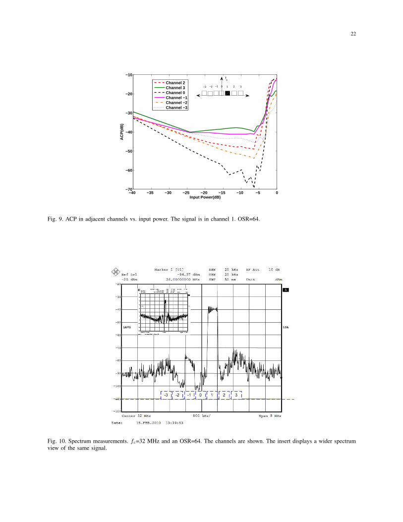
Fig. 9 shows a simulation plot of the input power (dB) against the ACP (dB) for the six
adjacent channels. The optimum input power is -7 dB, just before the onset of signal overload
in the Σ∆ converters. It can be observed that channel 3 has the highest noise as it represents
the third harmonic. Channel -1 represents the image and has the second highest noise. Channel
0 has lower noise than channel 2 as channel 0 is centered at fc. The maximum attenuation of
quantisation noise occurs around that region as the NTF of the Σ∆ operates from fc.
Table 1 helps to further illustrate the effect of offset on ACP. It gives a comparison of ACP
values for Cartesian Σ∆ with offset and without offset. The values were obtained at an input
power of -7 dB. Shifting the signal to channel 1 increases the noise in all channels. Those
channels containing the odd harmonics are particularly affected with noise increases of 20 dB
(channel 3), 15 dB (channel -1) and 13 dB (channel -3). A reduction in the noise can be seen
in the channel 0 as the NTF of the Σ∆ operates from fc. A higher oversampling rate will be
required to meet the WLAN standard (ACP <-40 dB) or fc can be increased to reduce the
relative offset frequency. Increasing fc by 2.5 will reduce the main interference channels by 8
dB which should then meet the WLAN specification. Alternatively, the WLAN standard is easily
met if the signal is not shifted to the adjacent channels. In fact, in this case the OSR can even
be reduced from 64 to a value as low as eight [15].
Spectrum measurement was performed using multi-carrier signals to further substantiate our
findings. An OFDM signal with an input power of -7 dB was programmed into the data timing
generator. A 3-level waveform (Fig. 2) was used as it suppresses the even harmonics. Fig. 10

15
Channels No. -3 -2 -1 0 1 2 3ACP (dB) no off-set
-57 -59 -54 Data -55 -59 -57
ACP(dB) 1 chan-nel offset
-44 -50 -39 -69 Data -47 -37
TABLE IACP FOR CARTESIAN Σ∆ WITH OFFSET AND WITHOUT OFFSET. CHANNEL 0 IS CENTERED ON fc . OSR=64.
shows the spectrum analyser display for a pulse waveform with an OSR of 64. The images and
harmonics which arise as a result of the offset are clearly visible. The measured result agrees
with simulations, except for some small artifacts in channel 0 of the measured signal. The
discrepancies can be attributed to the limitation in the slew rate capability of the experimental
setup and the mismatches in the positive and negative going waveforms. The negative slope of
the signal image in channel -1 can be explained by the fact that OFDM is made up of many
individual tones. As the offset between the tones and fc increases, the size of the distortions
of each tone image increases as shown by Fig. 7. The third harmonic and the image of the
third harmonic are smeared over a number of channels, but most of the energy is concentrated
within channel 3 and -3 respectively. It is quite evident that the inband noise is dominated by
the distortions as a result of the ‘polar to PWM/PPM’ conversion whereas the out-of-band noise
is dictated by the noise shaping effect of the Σ∆. This is illustrated by the gradual rise in the
noise level at the extremities of the spectrum as shown by the wide span view (Fig. 10 insert).
VI. CONCLUSION
This paper has identified a problem occurring when quantised phase shifts are converted
to pulse positions in a digital ‘polar to PWM/PPM’ block. The quantisation in phase causes
significant distortion. This paper proposes a mathematical solution to predict the amplitude

16
and frequency of the distortion products. It also demonstrates that the distortion increases with
increasing offset frequency by almost 6 dB/octave. The offset frequency must be less that 1%
of fc to guarantee distortions less than -40 dB for narrowband signals (Fig. 7). Increasing the
OSR helps to alleviate the problem (-6 dB/octave), but it also reduces the maximum carrier
frequency. The use of higher order Σ∆ structures will not be effective either, since the PPM
distortion dominates the in-band spectrum. (Note: The ‘polar to PWM/PPM’ block is not enclosed
in the Σ∆ feedback loop.) A potential solution is to avoid quantising the phase by using analog
techniques [16] but this removes many of the advantages of this all-digital structure.
In a multi-carrier environment, measurements and simulations show that it is best to avoid
changing channels by offsetting the carrier frequency because of increasing adjacent channel
interference in odd harmonics channels. Some of the distortions can be cancelled by using a
bridge amplifier structure to give a three-level signal. In order to meet the WLAN standard, it
is preferable to accommodate any channel change by altering the system clock frequency, fclk,
in which case WLAN specifications can be met with a much reduced OSR.
REFERENCES
[1] www.ericsson.com/technology/whitepapers/sustainableenergy.pdf, accessed November 2009
[2] Stapleton, S.P.: ‘Class S Power Amplifiers for RF Systems (using Bandpass Delta-Sigma Modulators)’, Agilent EEsof
Design Seminar, Prod No. N3508A.
[3] Keyzer, J., Hinrichs, J., Metzger, A., Iwamoto, M., Galton, I., Asbeck, P.: ‘Digital Generation of RF signals for Wireless
Communications with Band-Pass Delta Sigma Modulation’, Proc. 2001 IEEE MTT-S Int. Microwave Symp. Dig., May
2001, pp 2127-2130.
[4] Keyzer, J., Uang, R., Sugiyama, Y., Iwamoto, M., Galton, I., Asbeck, P.M.: ‘Generation of RF Pulsewidth Modulated
Microwave Signals using Delta-Sigma Modulation’, Proc. 2002 IEEE MTT-S Int. Microwave Symp. Dig., June 2002, pp.
397-400.

17
[5] Asbeck, P., Galton, I., Keh-Chung Wang, Jensen, J.F., Oki, A.K., Chang, C.T.M.:‘Digital Signal Processing - Up to
Microwave Frequencies’, IEEE Trans. Microwave Theory and Techn., March 2002, 50,(30), pp 900-909.
[6] Raab, F.H., Asbeck, P., Cripps, S., Kenington, P.B., Popovic, Z.B., Pothecary, N., Sevic, J.F., Sokal, N.O.:‘Power amplifiers
and transmitters for RF and microwave’, IEEE Trans. Microwave Theory Tech., March 2002, 50,(3), pp 814-826.
[7] Jayaraman, A., Chen, P.F., Hanington, G., Larson, L., Asbeck, P.: ‘Generation of RF Pulsewidth Modulated Microwave
Signals using Delta-Sigma Modulation’, IEEE Microwave and Wireless Components Letters., 1998, 8, (3), pp 121-123.
[8] Frappe, A., Flament, A., Stefanelli, B., Cathelin, A., Kaiser, A.:‘All-digital RF signal generation for software defined radio’,
Proc. 4th European Conference on Circuits and Systems for Communications, July 2008, pp 236-239
[9] Helaoui, M., Hatami, S., Negra, R., and Ghannouchi, F.:‘A novel architecture of Delta-Sigma Modulator Enabling All-Digital
Multiband Multistandard RF Transmitters Design’, IEEE Trans. Circuits and Systems II., 2008, 55,(11), pp 1129-1133
[10] Bassoo, V., and Faulkner, M.: ‘Sigma Delta Digital Drive Signals for Switchmode Power Amplifiers’, Electronic Letters,
2008, 44,(22), pp 1299-1300.
[11] Bassoo, V., Mustafa, A., and Faulkner, M.: ‘Distortion Arising from Polar to PWM/PPM Conversion in an All Digital
Upconverter for Switching RF Power Amplifier’. Proc. IEEE IMS Int. Microwave Symposium, Boston, USA, June 2009,
pp. 1533-1536.
[12] Schreier, R., and Temes, G.C.: ‘Understanding Delta-Sigma Data Converters’ (Wiley-IEEE Press, 2004).
[13] Wagh, P., and Midya, P.: ‘High Efficiency Switched-Mode RF Power Amplifier’. Proc. 42nd Midwest Symposium on
Circuits and Systems, 1999, Vol. 2, pp. 1044-1047.
[14] Ifeachor, E., and Jervis, P.: ‘Digital Signal Processing : A practical Approach’ (Prentice Hall, 2002)
[15] Bassoo, V., Tom, K., Mustafa, A.K., Cijvat, E., Sjoland, H., and Faulkner, M.: ‘A Potential Transmitter Architecture for
Future Generation Green Wireless Base Station’, EURASIP Journal on Wireless Communication and Networking, 2009,
Article ID 821846, 8 pages, 2009. doi:10.1155/2009/821846
[16] Jeong, J., and Wang, E.Y.: ‘A Polar Delta-Sigma Modulation Scheme for High Efficiency Wireless Transmitters’. Proc.
IEEE IMS Int. Microwave Symposium, Honolulu, USA, June 2007, pp. 73-76.

18
Fig. 1. Proposed transmitter architecture
Fig. 2. Block diagram of Cartesian Σ∆. The Σ∆ filter operates at a sample rate of fs ≤ fc

19
Fig. 3. Illustrating the pulse stuffing effect required to effect a change in phase of the RF signal. (a) carrier reference signal, (b)to (i) signal with phase advanced transient. Here the phase is quantised into 8 increments.
Fig. 4. SSB generation from a bank of phase shifted oscillators

20
Fig. 5. SSB generation for mathematical analysis
Fig. 6. SSB output spectrum from a Cartesian Σ∆. The distortions are from the PWM/PPM image and third harmonic.(fc=1024MHz and fssb= 40 MHz)

21
0 10 20 30 40 50 60 70−70
−65
−60
−55
−50
−45
−40
−35
−30
−25
−20
Offset frequency, fssb (MHz)
Siz
e o
f im
age/
har
mo
nic
wrt
sig
nal
(dB
)
Second harmonic
Third harmonic
Image
Measured results
Calculated results
Simulated results
Fig. 7. SSB harmonics and image. Amplitude (relative to signals) vs. fssb. (OSR=32, fc=1024 MHz)
Fig. 8. Spectrum measurement. fc=1024 MHz, fssb=32 MHz, OSR=32
22
−40 −35 −30 −25 −20 −15 −10 −5 0−70
−60
−50
−40
−30
−20
−10
Input Power(dB)
AC
P(d
B)
Channel 2Channel 3Channel 0Channel −1Channel −2Channel −3
0−1−2−3 1 2 3
fc
Fig. 9. ACP in adjacent channels vs. input power. The signal is in channel 1. OSR=64.
Fig. 10. Spectrum measurements. fc=32 MHz and an OSR=64. The channels are shown. The insert displays a wider spectrumview of the same signal.