Embed Size (px)
Citation preview

Doctoral Thesis
Multilevel Converters: Topologies, Modelling, Space Vector Modulation Techniques and
Optimisations
University of Seville Electronic Engineering Department
Power Electronics Group
Author: José Ignacio León Galván Advisor: Prof. Leopoldo García Franquelo

2

3
To my family

4

5
CONTENTS: 1. Introduction and objectives
1.1. Introduction
1.2. Objectives
2. Multilevel Converter Topologies
2.1. Introduction
2.2. Multilevel Converter Topologies
2.2.1. Diode-Clamped Converter (DCC)
2.2.1.1. Advantages and disadvantages of DCC topology
2.2.2. Flying Capacitor Converter (FCC)
2.2.2.1. Flying capacitor voltage ratios
2.2.2.2. Advantages and disadvantages of FCC topology
2.2.3. Cascaded Converter
2.2.3.1. Different DC voltage source ratios in multilevel cascaded
converters
2.2.3.2. Advantages and disadvantages of Cascaded topology
2.3. Converter Connecting Configurations
2.3.1. Three-Leg Four-Wire Topologies
2.3.2. Three-Leg Four-Wire Topologies
2.3.3. Four-Leg Four-Wire Topologies
3. Multilevel Converter Models
3.1. Introduction
3.2. Diode-Clamped Converter Model
3.2.1. Three-Leg Three-Wire Diode-Clamped Converter Model
3.2.2. Three-Leg Four-Wire Diode-Clamped Converter Model
3.2.3. Four-Leg Four-Wire Diode-Clamped Converter Model
3.3. Flying Capacitor Converter Model

6
3.3.1. Three-Leg Three-Wire Flying Capacitor Converter Model
3.3.2. Three-Leg Four-Wire Flying Capacitor Converter Model
3.3.3. Four-Leg Four-Wire Flying Capacitor Converter Model
4. Modulation Techniques for Multilevel Converters
4.1. Introduction
4.2. Classic PWM modulations
4.3. Space Vector PWM Modulation
4.3.1. Three-Leg Three-Wire Topologies
4.3.2. Three-Leg Four-Wire Topologies
4.3.3. Four-Leg Four-Wire Topologies
5. Solving the balancing of the DC-Link capacitors in Multilevel Converters
5.1. Introduction
5.2. Quasi-solution of the balancing problem
5.3. Balancing problem depending on the converter topology
5.3.1. Diode-Clamped Converter Topology
5.3.1.1. N-level Three-Leg Three-Wire Diode-Clamped Converter
Topology
5.3.1.2. N-level Four-Leg Four-Wire Diode-Clamped Converter
Topology
5.3.1.3. N-level Three-Leg Four-Wire Diode-Clamped Converter
Topology
5.3.2. Flying Capacitor Converter Topology
5.4. Controllability limits
6. Contributions and General Conclusions
7. Future works
8. Publications derived from the thesis work
9. References
10. Acknowledgments

7

8
Chapter 1
Introduction and Objectives
1.1 Introduction
The Electronic Engineering Department at University of Seville has been
involved in multilevel converter topics during last 10 years. The research has
been focused on the development of new modulation strategies and new control
strategies [1]-[4]. The performance of this thesis has been the pinnacle of this
research and it would be the base for future multilevel converters research in our
department.

9
1.2 Objectives
The objectives in this thesis have been focused on improvements on multilevel
converter features. The first objective is centered on minimizing the
computational cost of the modulation strategy. In this thesis, the design of simple
and fast Space Vector Modulation (SVPWM) techniques reducing the
computational cost for different multilevel converter topologies is the first aim.
On the other hand, multilevel converters present problems to achieve the balance
of DC capacitors. The second objective of this thesis is the development of
simple and low-cost control strategies to get voltage balance based on the use of
redundant vectors using proposed SVPWM strategies. These control algorithms
should be completely generalized and they could be applied to different
multilevel converter topologies and for any number of levels.

10
Chapter 2
Multilevel Converter
Topologies
2.1 Introduction
This thesis is focused on the development of different modulation techniques and
several optimisations to improve some specific characteristics of multilevel
converters. But, in order to make the text understandable, it is necessary to make
a brief overview of the most common multilevel converter topologies introducing
the used nomenclature and the operation basis of this type of converters. So, this
chapter is dedicated to introduce the way of switching for multilevel converters
and to show the possible output voltages that can be achieved depending on the
choosing converter topology.
Multilevel converters present great advantages compared with typical and very
well known two-level converters [5][6]. These advantages are fundamentally

11
focused on improvements in the output signals quality and a nominal power
increase in the converter. These properties make multilevel converters very
attractive to the industry and nowadays, researchers all over the world are
spending great efforts trying to improve multilevel converters performance as the
control simplification and the performance of different optimisation algorithms in
order to enhance the Total Harmonic Distortion (THD) of the output signals, the
balancing of the DC capacitors voltage, the ripple of the load currents, …, etc.
For instance, nowadays researchers are centered on the harmonic elimination
using pre-calculated switching functions [7]-[11], the development of new
multilevel converter topologies (hybrids or new ones) and the development of
new control strategies. This thesis is not focused on the harmonic elimination
topic and the control strategies for the complete system are not discussed. New
topologies are not presented in this thesis but using common multilevel converter
topologies, new voltage strategies are proposed.
2.2 Multilevel Converter Topologies
In order to facilitate the understanding of the text, it is going to be presented the
state-of-art of the different multilevel converter topologies. Although there are a
large number of multilevel converter topologies in the literature, in this chapter
the most common topologies will be presented. The most typical multilevel
converter topologies are: Diode-Clamped Converter (DCC), Flying Capacitor
Converter (FCC), and Cascaded Converter. Several surveys of multilevel
converters have been published to present these topologies [12]-[19].

12
2.2.1 Diode-Clamped Converter (DCC)
In 1980s, power electronics concerns were focused on the converters power
increase (increasing voltage or current). In fact, Current Source Inverters were
the main focus for researchers in order to increase the current. However, other
authors began to work on the idea of increasing the voltage instead the current. In
order to achieve this objective, authors were developing new converter
topologies. In 1981, A. Nabae, I. Takahashi and H. Akagi presented a new
neutral-point-clamped PWM inverter (NPC-PWM) [20]. This converter was
based on a modification of the classic two-level converter topology. In
conventional two-level case (see Figure 2.1), each transistor must have at the
most a voltage stress equal to VDC and they should be dimensioned to tolerate
this voltage.
Figure 2.1. Two-level conventional converter
The proposed modification to get the three-level converter added two new
transistors per phase (see Figure 2.2). Using this new topology, each transistor
tolerates at the most a voltage equal to VDC/2. So, if these new transistors have

13
the same characteristics than the transistors in two-level case, the DC-Link
voltage can be doubled achieving a value equal to 2VDC.
But, this converter topology still has a problem. If transistors S1 and S2 are
switched on and transistors S3 and S4 are switched off, VDC voltage should be
equally shared between transistors S3 and S4. But, there is not any mechanism
that assures it. The solution of this problem appears thanks to use the “clamping
diodes”. In each phase, two diodes clamp each transistor voltage. Finally, in
Figure 2.2, a three-level Diode Clamped Converter (DCC) is shown. In this
converter topology, the DC-Link voltage is equally shared between capacitors C1
and C2.
Figure 2.2. Three-level Diode-Clamped Converter
It can be explained why this converter is named three-level converter. In order to
show it, possible switching configurations of this converter topology can be
presented. There are only three possible switching configurations in the three-
level DCC. Other switching possibilities are not allowed because they create

14
short-circuit in some DC-Link capacitor or they let the output opened. For
instance, if S1, S2 and S3 are switched on, a short-circuit is created in capacitor
C2. Besides, the voltage in transistor S4 is VDC being its maximum admissible
voltage equal to VDC/2. The possible switching configurations are shown in
TABLE 2.I. Only three possible output phase voltages with respect to 0 (middle
point of the DC-Link) appear using this converter and this is the reason to name
this converter as a “three-level” converter.
S1 S2 S3 S4 Phase-0 voltage
ON ON OFF OFF VDC/2
OFF ON ON OFF 0
OFF OFF ON ON -VDC/2
TABLE 2.I. Possible switching configurations in a three-level DCC
After introducing the three-level DCC topology, it can be extended trying to
achieve more levels in the output phase voltages with respect to 0 [21]. In order
to show it, a phase of a five-level DCC is represented in Figure 2.3. Now, using
this configuration there are more possible switching configurations and they can
be seen in TABLE 2.II.
S1 S2 S3 S4 S5 S6 S7 S8 Phase-0 voltage
ON ON ON ON OFF OFF OFF OFF VDC/2
OFF ON ON ON ON OFF OFF OFF VDC/4
OFF OFF ON ON ON ON OFF OFF 0
OFF OFF OFF ON ON ON ON OFF -VDC/4
OFF OFF OFF OFF ON ON ON ON -VDC/2
TABLE 2.II. Possible switching configurations in a five-level DCC

15
Figure 2.3. Single phase Five-level Diode-Clamped Converter
In general, for N-level DCC topology all the possible switching configurations
have N-1 adjacent transistors switched on in each phase and the possible output
phase voltages with respect to 0 take N discrete values in equally spaced out in
the voltage range -VDC/2, VDC/2.

16
2.2.1.1 Advantages and disadvantages of FCC topology
The main advantages of the DCC topology are:
• The number of capacitors is low compared with other topologies as the
flying capacitor converter. This fact is very important due to the cost of
these reactive devices.
• This topology does not require any transformer
• There is only one DC-Link bus
• The change between adjacent states is done changing only the state of two
transistors.
The main drawbacks of DCC topology are:
• The possibilities to control the balance of the DC-Link capacitors voltage
are limited. In fact, other topologies as the Flying Capacitor topology
present more possibilities to achieve the balance.
• This type of converter is still not a final product of companies as ABB,
Semikron, …, etc. Therefore, all the actual converters are “homemade”
custom design prototypes.
DCC topology has become very popular between researchers all over the world
and other hybrid topologies have been developed trying to improve the converter
features [22]-[24].
2.2.2 Flying Capacitor Converter (FCC)
Multilevel Flying Capacitor Converter (FCC) topology has been recently
introduced and it present advantages and disadvantages compared with other
multilevel topologies [25][26]. FCC topology uses several floating capacitors in
each phase that connect several points in the converter to achieve different
voltage levels in the output signals. This topology presents the floating capacitors
instead the clamped diodes of DCC topology. In Figure 2.4, a conventional three-
phase three-level FCC is shown.

17
Figure 2.4. Conventional three-phase three-level Flying Capacitor Converter
The topology can be extended trying to achieve more levels in the output phase
voltages with respect to 0. In order to show it, a phase of an extended FCC is
represented in Figure 2.5. All the switching configurations in FCC can be studied
using a systematic method. There is not a complete freedom in the transistors
switching in each phase. In fact, each transistor can be associated with other
transistor in the same phase forming different couples and only one of the
transistors in each couple can be switched on at the same time. Each transistors
couple forms one basic cell of the converter. If both transistors were switched on
at the same instant, a short-circuit would be created in the flying capacitor of the
basic cell. Multilevel FCC topology can be represented in a different way
showing that the converter can be built connecting several basic cells in series.
An M-cell single-phase FCC is achieved thanks to M basic cells connected in
series [26]. A FCC basic cell and the M-cell single phase FCC topology are
shown in Figure 2.6 and Figure 2.7 respectively.

18
Figure 2.5. Phase of an extended Flying Capacitor Converter

19
Figure 2.6. Basic flying capacitor cell
Figure 2.7. M-cell Flying Capacitor Converter Topology
The switching configurations study can be done defining each transistor couple
state in a basic cell as a binary value specifying if the couple state is low (the
lowest transistor of the basic cell is switched on) or high (the highest transistor of
the basic cell is switched on). So, for a single phase x M-cell FCC, binary factors
Hxi can be defined as follows:

20
0,1,...,
1,xi
xixi
S OFFH with i M
S ON=
= = =
(2.1)
So, in general, for M-cell FCC case, there are 2M-1 possible switching
configurations where Hxi with i=1, …, M marks the state of each transistors
couple in the basic cell i in the single phase x [27].
2.2.2.1 Flying capacitor voltage ratios
In general, for multilevel FCC, several flying capacitor voltages
Vx1:Vx2:Vx3:..:Vx(M-1) can be considered [27]. The first presented FCC topology
had floating capacitors voltage ratios equal to M-1:..:2:1 (named in this work
OFBCS voltage ratio). A four-cell single phase FCC using OFBCS voltage ratio
is shown in Figure 2.8 in order to show the ratio performance.
Figure 2.8. Four-cell single phase FCC using OFBCS voltage ratio

21
Using this voltages ratio, there are only four possible switching configurations in
each phase for two-cell single phase FCC and they are shown in TABLE 2.III
using basic cells binary values Hxi. Other possibilities are not allowed because
they create short-circuit in some capacitor or they let the output opened. It is
important to say that two different switching configurations achieve the same
output phase voltage with respect to 0. This is very important because this type of
converter has redundant switching configurations. It will be shown later that this
property can be used to improve the floating capacitors voltage control. From
TABLE 2.III it can be concluded that two-cell single phase FCC is a three-level
single phase FCC with one redundant switching configuration. The state of each
phase is denoted by an integer number where ‘0’ means that the output Vxo
voltage is the minimum voltage possible.
SX1 SX2 HX1 HX2 Phasex-0
voltage
Phasex
State
ON ON 1 1 VDC/2 2
ON OFF 1 0 0 1
OFF ON 0 1 0 1
OFF OFF 0 0 -VDC/2 0
Redundant switching
configurations
TABLE 2.III. Possible switching configurations in two-cell single phase FCC using OFBCS voltages ratio
The same calculations can be done using the four-cell single phase FCC topology
with OFBCS voltages ratio. In this case, there are more possible switching
configurations and they are shown in TABLE 2.IV. The calculation results show
that this topology achieves five different output voltage levels presenting several
redundant switching configurations. Using OFBCS voltages ratio, the number of

22
output levels (N) is the number of basic cells (M) plus one. In general, there is an
easy way to calculate the output phase voltage with respect to 0 thanks to the
couples binary values using OFBCS voltages ratio.
1
_
_2
M
x xii
DC DCout x
Phase State H
V VV Phase StateM
=
=
= ⋅ −
∑ (2.2)
HX1 HX2 HX3 HX4 Phasex-0 voltage Phasex_State
0 0 0 0 -VDC/2 0
0 0 0 1 -VDC/4 1
0 0 1 0 -VDC/4 1
0 0 1 1 0 2
0 1 0 0 -VDC/4 1
0 1 0 1 0 2
0 1 1 0 0 2
0 1 1 1 VDC/4 3
1 0 0 0 -VDC/4 1
1 0 0 1 0 2
1 0 1 0 0 2
1 0 1 1 VDC/4 3
1 1 0 0 0 2
1 1 0 1 VDC/4 3
1 1 1 0 VDC/4 3
1 1 1 1 VDC/2 4
TABLE 2.IV. Possible switching configurations in four-cell single phase FCC using OFBCS voltages ratio

23
It can be seen from TABLE 2.III and TABLE 2.IV that increasing the number of
cells of the converter, the switching configurations redundancy increases. This
redundancy implies that the same output phase voltage can be achieved thanks to
different switching configurations. This property does not appear in DCC and in
chapter 5 it will be shown that it introduces some control advantages. However, it
should not be forgotten that the control complexity increases with the number of
FCC cells because there will be more redundant switching configurations.
In [27] new flying capacitors voltage ratios were presented in order to achieve
more output voltage levels with the same number of power devices. In [27][28],
the comparison between these voltage ratios was presented using the Full Binary
Combination Schema (FBCS) concept demonstrating that, with the same number
of power devices, the number of levels in the output voltages changes depending
on the voltage ratios used in FCC. Several voltage ratios generate higher number
of levels compared with OFBCS. Therefore, at first sight, they improve the
behaviour of the converter because they achieve better output signals quality with
the same cost. However, all these possible configurations achieve phase to
middle point of the DC-Link output voltage signals in the range -VDC/2,VDC/2.
These voltage ratios consider that the flying capacitors voltages have the same
polarity. All the flying capacitors are charged with the desired voltage in the
same sense. A new voltage ratio is presented considering OFBCS voltage ratios
but doing that flying capacitors voltages can be positive or negative. In the
proposed voltage ratio, the sign of flying capacitor voltages (Vxi) is alternatively
positive and negative considering positive the DC-Link voltage. This proposed
voltage ratio is named New FBCS (NFBCS). In Figure 2.9, a FCC performed
with four basic cells using NFBCS is shown.

24
Figure 2.9. Four-cell single phase FCC using NFBCS voltages ratio
Using this voltage configuration, the output phase to middle point of DC-Link
voltage (Vx0) can be calculated. In TABLE 2.V, the results using OFBCS and
NFBCS voltage ratios are shown. It can be seen that with the same number of
devices (only with 4 basic cells), OFBCS achieves five output levels and NFBCS
achieves 15 levels. So, it is clear that using this new voltages ratio, with the same
number of power devices, the number of output voltage levels increases. Other
important result can be concluded from TABLE 2.V. Using OFBCS, output Vx0
voltages are located in the range -VDC/2, VDC/2 where VDC is the DC-Link
voltage. However, using NFBCS voltages ratio the output voltages are in the
range -2VDC, 2VDC with the same DC-Link voltage. Therefore, two clear
advantages appear using NFBCS voltage ratio.
In general, for a M-cell FCC using OFBCS voltages ratio, the number of output
levels is N=M+1. However, using NFBCS the number of levels increases
exponentially. In Figure 2.10, the number of output levels achieved by both
voltage ratios is represented in order to show the increase of levels using NFBCS
voltages ratio.

25
Output Phasex-middle
point of DC-Link
Voltage/VDC
Switching
Configuration
HX1HX2HX3HX4 OFBCS NFBCS
0000 -1/2 -1/2
0001 -1/4 -3/4
0010 -1/4 1/4
0011 0 0
0100 -1/4 -7/4
0101 0 -2
0110 0 -1
0111 1/4 -5/4
1000 -1/4 5/4
1001 0 1
1010 0 2
1011 1/4 7/4
1100 0 0
1101 1/4 -1/4
1110 1/4 3/4
1111 1/4 1/2
TABLE 2.V. Output voltages for four-cell FCC using OFBCS and NFBCS voltages ratios

26
Figure 2.10. Number of levels achieved by OFBCS and NFBCS voltages ratios depending of the number of FCC basic cells
Output voltages Vx0 range also depends on the chosen voltages ratio. Using
OFBCS, Vx0 is always in the range -VDC/2, +VDC/2 and this range does not
depend on the number of basic cells in FCC. However, using NFBCS the output
voltage range increases. In Figure 2.11, the output voltage range depending on
the used voltages ratios is represented showing the increase depending on the
number of basic cells in the FCC.
Previously, the advantages using NFBCS in FCC have been shown. However,
some possible drawbacks appear using this new voltages ratio. Changing the sign
of flying capacitor voltages, the power semiconductors of the converter should be
chosen very carefully. Using OFBCS, each power device must support a
maximum voltage equal to VDC/M where M is the number of basic cells in the
FCC. But using NFBCS voltage ratio, each power device must support higher
voltages and due to this fact, the specifications of each power device must be
chosen in order to support this voltage. For an M-cell FCC using NFBCS, the
maximum voltage that each power device must support is (2M-1)VDC/M. This
problem also appears using other previously published voltage ratios [28].

27
Figure 2.11. Maximum output voltage obtained by OFBCS and NFBCS voltage ratios depending of the number of FCC basic cells
On the other hand, the topology of power devices using NFBCS voltages ratio
must be different because they must be bidirectional. Actually these bidirectional
power devices are used in other converter topologies as matrix converters and
they can be found easily in the market [29]. These bidirectional power devices
use to be diode bridges or back-to-back switches. The diagram of a back-to-back
switch is shown in Figure 2.12 and it is built using a module of two reverse
blocking IGBTs. This module controls the current flow within each switch.
These power devices are actually well extended and for instance, bidirectional
power devices are performed by Dynex Semiconductors, Semelab or EUPEC.

28
Figure 2.12. Back-to-back bidirectional switch
As it was shown before, using NFBCS voltages ratio it is achieved a higher
number of output voltage levels (see TABLE 2.V). However, these output
voltage levels are not equally spaced out. This can lead to an increase in the
ripple in the output voltage signals due to the fact that there are different voltage
steps between the possible output voltage levels. In order to minimize this
problem, other voltage ratios can be taken into account. It can be considered a
new voltages ratio similar to NFBCS but doing all the flying capacitors voltages
equal to VDC/M where M is the number of basic cells of the FCC. This new ratio
is named NEFBCS. In Figure 2.13, a four-cell FCC using NEFBCS voltages ratio
is shown. All possible output Vx0 voltages can be easily determined and they are
shown in TABLE 2.VI.
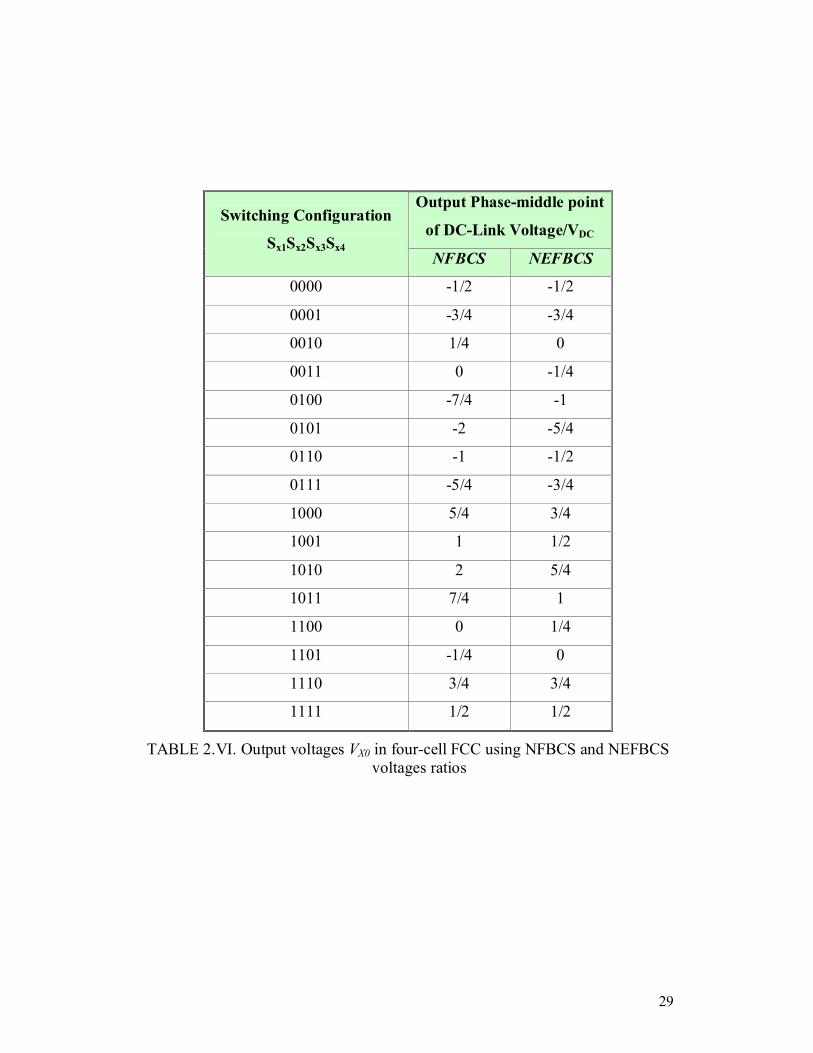
From TABLE 2.VI, it can be seen that output voltage levels are equally spaced
out and all the voltage steps are equal to VDC/M. However, NEFBCS ratio makes
smaller the output voltage range. In general, for a M-Cell FCC the output voltage
range is (-3/2+1/M)VDC,(-3/2+1/M)VDC. So, it can be seen that increasing the
number of basic cells, the maximum output voltage using NEFBCS is smaller
than the obtained using NFBCS. Besides, the number of output voltage levels
depends on the chosen voltages ratio. Figure 2.14 and Figure 2.15 show a
comparison between OFBCS, NFBCS and NEFBCS voltages ratios.
29
Output Phase-middle point
of DC-Link Voltage/VDC Switching Configuration
Sx1Sx2Sx3Sx4 NFBCS NEFBCS
0000 -1/2 -1/2
0001 -3/4 -3/4
0010 1/4 0
0011 0 -1/4
0100 -7/4 -1
0101 -2 -5/4
0110 -1 -1/2
0111 -5/4 -3/4
1000 5/4 3/4
1001 1 1/2
1010 2 5/4
1011 7/4 1
1100 0 1/4
1101 -1/4 0
1110 3/4 3/4
1111 1/2 1/2
TABLE 2.VI. Output voltages VX0 in four-cell FCC using NFBCS and NEFBCS voltages ratios

30
Figure 2.13. Four-cell single phase FCC using NEFBCS voltages ratio
Figure 2.14. Maximum output voltage depending on the number of basic cells in
FCC using different flying capacitor voltage ratios

31
Figure 2.15. Number of output voltage levels depending on the number of basic
cells in the FCC using different flying capacitor voltage ratios
As conclusions, new flying capacitor voltages ratios using the Full Binary
Combination Schema (FBCS) have been studied in order to improve the output
signals features for multilevel FCC. These voltage ratios use positive and
negative flying capacitor voltages. The results show that an increase in the output
voltages range and an increase in the number of levels of the converter is
achieved with the same number of power devices and with the same DC-Link
capacitors voltage. Therefore, to obtain the same maximum output voltage, the
DC-Link capacitors voltage can be reduced and the power devices can have
lower voltage requirements. Besides, discussions about the physical
implementation and possible drawbacks of these voltage ratios have been
introduced.

32
2.2.2.2 Advantages and disadvantages of FCC topology
Finally, the main advantages of the FCC topology are:
• This topology presents more possibilities to control the DC-Link
capacitors voltage compared with other multilevel topologies using the
redundant switching configurations.
• This topology does not require any transformer
The main drawbacks of FCC topology are:
• The number of capacitors is high compared with other topologies as the
diode clamped converter. This fact is very important due to the cost of
these reactive devices.
• The change between adjacent states is done changing the states of one
several transistors. This fact increases the number of commutations in the
transistors and the power losses in the converter.
• The clamping capacitors must be set up with the required voltage levels.
So, there is necessary an initialization of the converter.
• This type of converter is still not a final product of companies as ABB,
Semikron, …, etc. Therefore, all the actual converters are “homemade”
custom design prototypes.
2.2.3 Cascaded Converter
The cascaded converter or full-bridge converter is formed by two single-phase
inverters with independent voltage sources [30]. In Figure 2.16, a phase of a
three-level cascaded converter is shown.

33
Figure 2.16. Phase of the three-level cascaded converter
Considering the three-level basic cell, it is clear that only one transistor of each
leg (S1-S1’, S2-S2’) can be switched on at the same time. In order to facilitate the
notation of the possible switching configurations, for each basic cell in phase x,
binary factors Hxi can be defined as follows:
'
'
0,
1,xi xi
xixi xi
S ON and S OFFH
S OFF and S ON
= == = = (2.3)
So, using this binary notation, the possible switching configurations of the three-
level basic cell are shown in TABLE 2.VII.

34
HX1 HX2 VAB
0 0 0
0 1 -VDC
1 0 VDC
1 1 0
TABLE 2.VII. Possible switching configurations in a three-level cascaded converter using the binary notation
This three-level converter is the basic cell that is used to build multilevel
cascaded converters. A multilevel cascaded converter is easily built connecting
basic three-level cells in series. For instance, the two basic cells cascaded
converter is shown in Figure 2.17. It is important to notice that each basic cell
needs an independent voltage source and this is one of the most important
drawbacks of this multilevel converter topology.
Figure 2.17. Two basic cells cascaded converter

35
2.2.3.1 Different DC voltage source ratios in multilevel cascaded
converters
The cascaded converter topology has the same property than FCC topology.
Different DC voltage source ratios can be applied in order to achieve different
voltage levels in the output signals [31]. The classic cascaded converter assumes
that all the DC voltage sources have exactly the same value.
Assuming conventional voltage sources ratio and considering the two basic cells
cascaded converter, the possible switching configurations are shown in TABLE
2.VIII. The phase state can be defined as the voltage level achieved by the
converter where 0 means the lowest voltage level. This converter achieves five
possible output voltages and, therefore it is a five-level converter.
Analytically, it is easy to know the output phase-to-neutral voltage and the phase
state defining the FCxi parameter for M-cell cascaded converter as:
( 1)
( 1)
( 1)
0,1, 0 1 1,...,
1, 1 0
xi x i
xi xi x i
xi x i
H HFC H and H with i M
H and H
+
+
+
== − = = =
= =
(2.4)
And finally, the phase state and the output phase-to-neutral voltages can be
determined using the FCxi parameter as follows:

36
1
1
_
_
M
x xii
M
xn DC x DC DC xii
Phase State M FC
V V Phase State MV V FC
=
=
= −
= ⋅ − = −
∑
∑ (2.5)
Cell 1 Cell 2
HX1 HX2 HX3 HX4 Vxn voltage Phasex_State
0 0 0 0 0 2
0 0 0 1 VDC 3
0 0 1 0 -VDC 1
0 0 1 1 0 2
0 1 0 0 VDC 3
0 1 0 1 2VDC 4
0 1 1 0 0 2
0 1 1 1 VDC 3
1 0 0 0 -VDC 1
1 0 0 1 0 2
1 0 1 0 -2VDC 0
1 0 1 1 -VDC 1
1 1 0 0 0 2
1 1 0 1 VDC 3
1 1 1 0 -VDC 1
1 1 1 1 0 2
TABLE 2.VIII. Output voltages for a two basic cells cascaded converter using classic voltage ratio (all DC voltage sources have the same value)

37
Using classic voltage sources ratio, a diagram of the necessary basic cells to
obtain multilevel cascaded converters is shown in Figure 2.18. The number of
three-level basic cells to build a N-level cascaded converter is (N-1)/2 with N
odd.
Figure 2.18. Diagram of the necessary basic three-level cells to obtain different multilevel single-phase cascaded converters

38
Other DC voltage sources ratios can be taken into account [31]. A generalized
study can be done for the two basic cells single phase cascaded converter. In this
case, the possible output phase-to-neutral voltages can be calculated and they are
shown in TABLE 2.IX.
Cell 1 Cell 2
HX1 HX2 HX3 HX4 Vxn voltage
0 0 0 0 0
0 0 0 1 VDC2
0 0 1 0 -VDC2
0 0 1 1 0
0 1 0 0 VDC1
0 1 0 1 VDC1+ VDC2
0 1 1 0 VDC1- VDC2
0 1 1 1 VDC1
1 0 0 0 -VDC1
1 0 0 1 VDC2- VDC1
1 0 1 0 -VDC1 -VDC2
1 0 1 1 -VDC1
1 1 0 0 0
1 1 0 1 VDC2
1 1 1 0 -VDC2
1 1 1 1 0
TABLE 2.IX. Generalized output phase-to-neutral voltages for a two basic cells single phase cascaded converter

39
So, depending on the DC voltage sources values, different number of levels can
be obtained in the output voltages. For instance, if VDC2 is three times VDC1, nine
different levels appear in the output voltages. It can be seen in TABLE 2.X.
Cell 1 Cell 2
HX1 HX2 HX3 HX4 Vxn voltage Phasex_State
0 0 0 0 0 4
0 0 0 1 3VDC1 7
0 0 1 0 -3VDC1 1
0 0 1 1 0 4
0 1 0 0 VDC1 5
0 1 0 1 4VDC1 8
0 1 1 0 -2VDC1 2
0 1 1 1 VDC1 5
1 0 0 0 -VDC1 3
1 0 0 1 2VDC1 6
1 0 1 0 -4VDC1 0
1 0 1 1 -VDC1 3
1 1 0 0 0 4
1 1 0 1 3VDC1 7
1 1 1 0 -3VDC1 1
1 1 1 1 0 4
TABLE 2.X. Output phase-to-neutral voltages for a two basic cells single phase cascaded converter considering VDC2=3VDC1

40
It is important to notice that depending on the chosen DC voltage sources ratio,
the number of output voltage levels change. Besides, the switching
configurations redundancy also depends on the DC voltage sources ratio. So, the
cascaded converter topology behavior is similar to FCC topology because both
converter topologies can apply different voltage ratios depending on the needed
industrial application.
2.2.3.2 Advantages and disadvantages of cascaded converter
topology
The main advantages of the Cascaded Converter topology are:
• This topology is based on basic cells (full-bridge converters) connected
each other. So, its modularity is important and the controller can be
distributed. This makes for a simpler controller structure than for either of
the two previously discussed topologies.
• This type of converters is a final product of companies as ABB, Semikron,
…, etc. Therefore, the cost of using this type of converters is lower
because other topologies are completely custom made.
The main drawback of Cascaded Converter topology is:
• This topology has not been applied at low power levels to date because of
the need to provide separate isolated DC supplies for each full-bridge
converter element.

41
2.3 Converter Connecting Configurations
2.3.1 Three-Leg Three-Wire Topologies
In previous points of this chapter, the most common multilevel converter
topologies have been presented showing all possible switching configurations in
each converter phase. In the same way, Three-phase systems can be developed
thanks to use three single phase converters. Three-leg three-wire (3L3W)
converter topologies are defined as three-phase converters connected to a three-
phase load with the neutral point of the load unconnected. For instance, a 3L3W
three-level diode-clamped converter is shown in Figure 2.19.
Figure 2.19. 3L3W three-level Diode-clamped converter
42
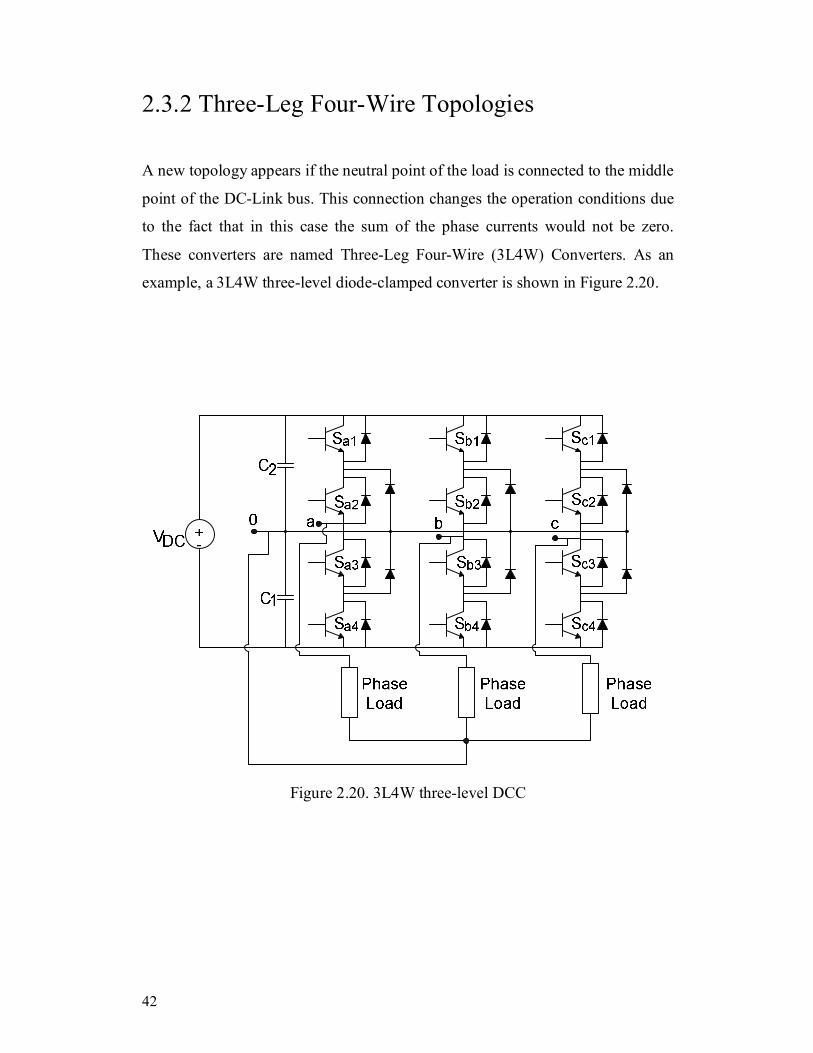
2.3.2 Three-Leg Four-Wire Topologies
A new topology appears if the neutral point of the load is connected to the middle
point of the DC-Link bus. This connection changes the operation conditions due
to the fact that in this case the sum of the phase currents would not be zero.
These converters are named Three-Leg Four-Wire (3L4W) Converters. As an
example, a 3L4W three-level diode-clamped converter is shown in Figure 2.20.
Figure 2.20. 3L4W three-level DCC

43
2.3.3 Four-Leg Four-Wire Topologies
A new topology can be developed connecting the neutral point of the load to a
new phase of the converter (the fourth leg). These converters are named Four-
Leg Four-Wire (4L4W) Converters. In this case, as in 3L4W case, it is clear that
the sum of the phase currents would not be zero. But now, there are several
possibilities to connect the neutral point of the load depending on the switching
configuration of the fourth leg. As an example, a 4L4W two-level conventional
converter is shown in Figure 2.21.
Figure 2.21. Four-Leg Four-Wire two-level conventional converter

44
Chapter 3
Multilevel Converter Models
3.1 Introduction
It is very important to develop mathematical models for multilevel converters to
carry out simulations to find out the system response to different control
strategies. In fact, the first step of the implementation of a control algorithm is to
simulate it and to see if the simulation results are satisfactory. In this thesis,
several multilevel converters analytical models have been developed. These
models are built thanks to commutation models and the definition of the
switching functions that will be presented in this chapter. The simulation models
were developed using MatLab/Simulink® software helping to the performance of
the control algorithms presented in this thesis. All mathematical models are
based on the determination of state equations for dynamical variables introduced
in [1]. These models are conspicuous by their extreme simplicity in front of other
previous analytical models presented in the literature [32]-[36].

45
In order to introduce the commutation model of a multilevel converter, a phase of
the very well known conventional two-level converter is shown in Figure 3.1.
Figure 3.1. Phase of the conventional two-level converter
In this converter, only one of the transistors can be switched on at the same time.
If S1 transistor is switched on, the output phase voltage with respect to the
reference (see figure 3.1) is VDC/2 and if S2 transistor is switched on, the output
phase voltage with respect to the reference is -VDC/2. In order to simplify the
circuit, it is possible to replace the phase using an ideal switch that connects the
output to the possible voltage connection points of the system. The switching
functions are defined as Sij where i is the phase and j is the point where the phase
i output is connected (it is supposed that 0 is the lowest voltage connection
value). The switching function Sij is equal to “1” if the phase i is connected to the
voltage connection point j and “0” if the phase i is connected to other voltage
connection point. The simplification of the two level single phase converter can
be seen in Figure 3.2.

46
Figure 3.2. Phase of the conventional two-level converter using an ideal switch
This type of commutation model using switching functions simplifies the
graphical display of multilevel converters and is completely generalized because
any type of transistors can be considered in the system. In this way, the study of
multilevel converters is completely generalized obtaining the simulation results
using ideal switches. Some transistors real effects as the turn-on time, turn-off
time, internal resistance, internal losses, …, etc, are neglected. However, the
main advantage of this type of commutation model is its simplicity and its easy
implementation in simulation softwares in order to study complex systems as
multilevel converters.
The implemented analytical models need the state equations for the DC
capacitors voltages and the phase currents. This chapter is focused on the
determination of these state equations depending on the multilevel converter
topology. Using matrix notation, the state equations can be described as follows.
11 1
JxJxJ Jx Jx DC
dW A W B Vdt
= + (3.1)

47
3.2 Diode-Clamped Converter (DCC) Model
3.2.1 Three-Leg Three-Wire Diode-Clamped Converter
(3L3W-DCC) Model
Figure 3.3 shows the commutation model of a three-phase 3L3W three-level
DCC. As a three level converter, it can be seen that each phase can be connected
to level 0, 1 or 2. The mathematical model uses the switching functions Sij for i Є
a,b,c and j Є 0,1,2.
Figure 3.3. Commutation model of three-level Diode-Clamped Converter
3L3W Three-level DCC can be easily extended increasing the number of levels.
The commutation model of the 3L3W N-level DCC is shown in Figure 3.4. In
the N-level case, the mathematical model uses switching functions Sij where i Є
a,b,c and j Є 0,1,…, N-1.
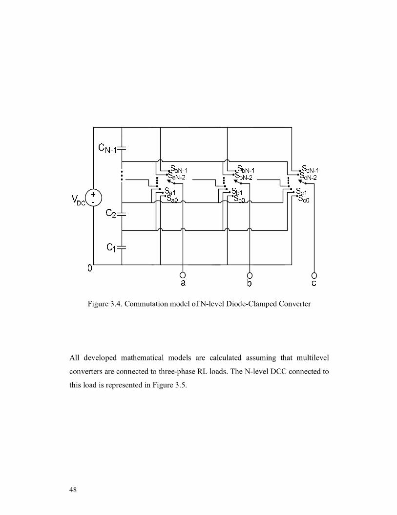
48
Figure 3.4. Commutation model of N-level Diode-Clamped Converter
All developed mathematical models are calculated assuming that multilevel
converters are connected to three-phase RL loads. The N-level DCC connected to
this load is represented in Figure 3.5.

49
Figure 3.5. Commutation model of a three-level 3L3W Diode-Clamped Converter connected to a RL load
In general for N-level DCC, the currents that flow through the DC-Link
capacitors can be determined using the switching functions.
− − − −
− − − −
− − −= =− − − − − − − − −
− − − − − −− −
= = − − − − − − − −− − − − − −
−= = + − − −
− − −
111 1 1 2 3 4 3 2
2
212 2 1 2 3 4 3 2
2
33 3 1 2 3
2 3 4 1 3 2 1... ...1 1 1 2 1 1 1
1 3 4 1 3 2 1... ...1 1 1 2 1 1 1
1 2 4 ...1 1 1
CN N N N
CN N N N
C
dV N N Ni C F F F F F F Fdt N N N N N NdV N Ni C F F F F F F Fdt N N N N N N
dV Ni C F F Fdt N N N − − − −
− − − −
−−− − − −
− − − −− − −
= = + + − − − − − −− − − − − −
− − −= = + + + + + + + −
− − − − −
1 4 3 22
414 4 1 2 3 4 3 2
2
( 1)11 1 1 2 3 4 3
2
1 3 2 1...2 1 1 1
1 2 3 1 3 2 1... ...1 1 1 2 1 1 1
.....1 2 3 1 4 3 2... ...
1 1 1 2 1 1
N N N N
CN N N N
C NNN N N N
F F F FN N N
dVi C F F F F F F Fdt N N N N N N
dV N N Ni C F F F F F Fdt N N N N N −− 21 NF
N
(3.2)
50
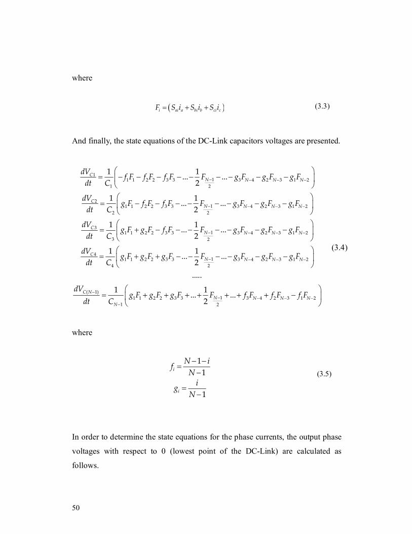
where
( )= + +i ai a bi b ci cF S i S i S i (3.3)
And finally, the state equations of the DC-Link capacitors voltages are presented.
− − − −
− − − −
− − − −
= − − − − − − − − −
= − − − − − − − −
= + − − − − − − −
111 1 2 2 3 3 3 4 2 3 1 2
1 2
211 1 2 2 3 3 3 4 2 3 1 2
2 2
311 1 2 2 3 3 3 4 2 3 1 2
3 2
1 1... ...2
1 1... ...2
1 1... ...2
CN N N N
CN N N N
CN N N N
dV f F f F f F F g F g F g Fdt C
dV g F f F f F F g F g F g Fdt C
dV g F g F f F F g F g F g Fdt C
− − − −
−− − − −
−
= + + − − − − − −
= + + + + + + + −
411 1 2 2 3 3 3 4 2 3 1 2
4 2
( 1)11 1 2 2 3 3 3 4 2 3 1 2
1 2
1 1... ...2
.....
1 1... ...2
CN N N N
C NN N N N
N
dV g F g F g F F g F g F g Fdt C
dVg F g F g F F f F f F f F
dt C
(3.4)
where
− −=
−
=−
i
i
N ifN
igN
11
1
(3.5)
In order to determine the state equations for the phase currents, the output phase
voltages with respect to 0 (lowest point of the DC-Link) are calculated as
follows.

51
− − −
− − −
= + + + + + + +
+ + + + + −
= + + + + + + +
+ + + + + −
= +
0 1 1 2 1 2 3 1 2 3
( 2) 1 2 ( 2) ( 1)
0 1 1 2 1 2 3 1 2 3
( 2) 1 2 ( 2) ( 1)
0 1 1 2
( ) ( ) ...
( ... )
( ) ( ) ...
( ... )
(
a a C a C C a C C C
aa N C C C N a N DC
b b C b C C b C C C
bb N C C C N b N DC
c c C c
V S V S V V S V V VdiS V V V S V Ldt
V S V S V V S V V VdiS V V V S V Ldt
V S V S V
− − −
+ + + + + +
+ + + + + −
1 2 3 1 2 3
( 2) 1 2 ( 2) ( 1)
) ( ) ...
( ... )
C C c C C C
cc N C C C N c N DC
V S V V VdiS V V V S V Ldt
(3.6)
3L3W topology fulfils that the voltage of the neutral point of the load with
respect to 0 is determined as follows.
0 0 00 3
a b cN
V V VV + +=
(3.7)
The phase voltages with respect to the neutral point of the load are determined.
= − == − == − =
0 0
0 0
0 0
aN a N a a
bN b N b b
cN c N c c
V V V R iV V V R iV V V R i
(3.8)
And finally, the phase currents state equations are presented.

52
− − −
− − −
− − −
= − + + + − + + − + + +
+ + + − + + − + + +
+ + + − + + − + +
11 ( 2) 1 ( 2) 1 ( 2)
22 ( 2) 2 ( 2) 2 ( 2)
33 ( 2) 3 ( 2) 3 ( 2
2( ... ) ( ... ) ( ... )3
2( ... ) ( ... ) ( ... )3
2( ... ) ( ... ) ( ...3
a a Ca a a N b b N c c N
Ca a N b b N c c N
Ca a N b b N c c N
di R Vi S S S S S Sdt L L
V S S S S S SL
V S S S S S SL
−− − −
− − −
− − −
− −
+
+ +
+ − − +
+ − −
= − + − + + + + + − + + +
+ − + + + + +
)
( 2)( 2) ( 2) ( 2)
( 1) ( 1) ( 1)
11 ( 2) 1 ( 2) 1 ( 2)
22 ( 2) 2 ( 2
)
...
(2 )3
(2 )3
( ... ) 2( ... ) ( ... )3
( ... ) 2( ...3
C Na N b N c N
DCa N b N c N
b b Cb a a N b b N c c N
Ca a N b b N
VS S S
LV S S S
Ldi R Vi S S S S S Sdt L L
V S S S SL −
− − −
−− − −
− − −
−
− + + +
+ − + + + + + − + + +
+ +
+ − + − +
+ − + −
= − + − + +
) 2 ( 2)
33 ( 2) 3 ( 2) 3 ( 2)
( 2)( 2) ( 2) ( 2)
( 1) ( 1) ( 1)
11 (
) ( ... )
( ... ) 2( ... ) ( ... )3
...
( 2 )3
( 2 )3
( ...3
c c N
Ca a N b b N c c N
C Na N b N c N
DCa N b N c N
c c Cc a a N
S S
V S S S S S SL
VS S S
LV S S S
Ldi R Vi S Sdt L L − −
− − −
− − −
−−
− + + + + + +
+ − + + − + + + + + +
+ − + + − + + + + + +
+ +
+ −
2) 1 ( 2) 1 ( 2)
22 ( 2) 2 ( 2) 2 ( 2)
33 ( 2) 3 ( 2) 3 ( 2)
( 2)( 2
) ( ... ) 2( ... )
( ... ) ( ... ) 2( ... )3
( ... ) ( ... ) 2( ... )3
...
(3
b b N c c N
Ca a N b b N c c N
Ca a N b b N c c N
C Na N
S S S S
V S S S S S SL
V S S S S S SL
VS
L − −
− − −
− + +
+ − − +
) ( 2) ( 2)
( 1) ( 1) ( 1)
2 )
( 2 )3
b N c N
DCa N b N c N
S S
V S S SL
(3.9)
53
3.2.2 Three-Leg Four-Wire Diode-Clamped Converter
(3L4W-DCC) Model
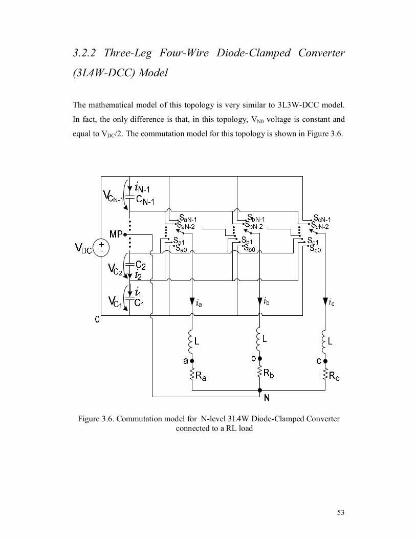
The mathematical model of this topology is very similar to 3L3W-DCC model.
In fact, the only difference is that, in this topology, VN0 voltage is constant and
equal to VDC/2. The commutation model for this topology is shown in Figure 3.6.
Figure 3.6. Commutation model for N-level 3L4W Diode-Clamped Converter connected to a RL load

54
So, the expressions presented for the 3L3W topology are valid but imposing that
VN0 is equal to the middle DC-Link voltage. Hence, state equations for the DC-
Link capacitors voltage for 3L4W DCC are (3.4). Nevertheless, the phase
currents state equations change due to the presence of the fourth wire connecting
the neutral point of the load with the middle point of the DC-Link. So, using
3L4W-DCC topology, the phase voltages with respect to the neutral point of the
load can be determined.
= − =
= − =
= − =
0
0
0
2
2
2
DCaN a a a
DCbN b b b
DCcN c c c
VV V R i
VV V R i
VV V R i
(3.10)
And finally, the phase currents state equations are presented.
− −
− − −
− −
− − −
= − − + + + + + + +
+ + +
= − − + + + + + + +
+ + +
=
1 1 ( 2) 2 2 ( 2)
( 2) ( 2) ( 1)
1 1 ( 2) 2 2 ( 2)
( 2) ( 2) ( 1)
1 ( ... ) ( ... )2
...
1 ( ... ) ( ... )2
...
a a DCa C a a N C a a N
C N a N DC a N
b b DCb C b b N C b b N
C N b N DC b N
c
di R Vi V S S V S Sdt L L L
V S V S
di R Vi V S S V S Sdt L L L
V S V S
didt − −
− − −
− − + + + + + + +
+ + +
1 1 ( 2) 2 2 ( 2)
( 2) ( 2) ( 1)
1 ( ... ) ( ... )2
...
c DCc C c c N C c c N
C N c N DC c N
R Vi V S S V S SL L L
V S V S
(3.11)

55
3.2.3 Four-Leg Four-Wire Diode-Clamped Converter
(4L4W-DCC) Model
The commutation model of the 4L4W N-level DCC is shown in Figure 3.7. The
commutation model has been validated connecting the converter to a R-L load.
This system is going to be described in detail.
Figure 3.7. Commutation model for N-level 4L4W Diode-Clamped Converter connected to a RL load
It can be seen that the DC-Link capacitors voltages state equations can be
determined using (3.4) where fi and gi were defined in (3.5) but assuming that Fi
functions can be determined as follows.

56
= + + + = − + − + −( ) ( ) ( )i ai a bi b ci c di N ai di a bi di b ci di cF S i S i S i S i S S i S S i S S i
(3.12)
On the other hand, the voltage of the neutral point of the load with respect to 0
(lowest point of the DC-Link) can be determined.
0 1 1 2 1 2 3 1 2 3
( 2) 1 ( 2) ( 1)
( ) ( ) ...( ... )
N d C d C C d C C C
d N C C N d N DC
V S V S V V S V V VS V V S V− − −
= + + + + + + +
+ + + +
(3.13)
The phase voltages with respect to 0 are calculated thanks to expression (3.6) and
finally, using (3.8), the phase currents state equations are presented.

57
− −
− −
− −
−− −
− −
= − + + + − + + +
+ + + − + + +
+ + + − + + + +
+ − +
+ −
11 ( 2) 1 ( 2)
22 ( 2) 2 ( 2)
33 ( 2) 3 ( 2)
( 2)( 2) ( 2)
( 1) ( 1)
( ... ) ( ... )
( ... ) ( ... )
( ... ) ( ... ) ...
a a Ca a a N d d N
Ca a N d d N
Ca a N d d N
C Na N d N
DCa N d N
di R Vi S S S Sdt L L
V S S S SL
V S S S SL
VS S
LV S S
L
− −
− −
− −
−− −
−
= − + + + − + + +
+ + + − + + +
+ + + − + + + +
+ − +
+ −
11 ( 2) 1 ( 2)
22 ( 2) 2 ( 2)
33 ( 2) 3 ( 2)
( 2)( 2) ( 2)
( 1) (
( ... ) ( ... )
( ... ) ( ... )
( ... ) ( ... ) ...
b b Cb b b N d d N
Cb b N d d N
Cb b N d d N
C Nb N d N
DCb N d
di R Vi S S S Sdt L L
V S S S SL
V S S S SL
VS S
LV S S
L −
− −
− −
− −
−− −
−
= − + + + − + + +
+ + + − + + +
+ + + − + + + +
+ − +
+
1)
11 ( 2) 1 ( 2)
22 ( 2) 2 ( 2)
33 ( 2) 3 ( 2)
( 2)( 2) ( 2)
( 1)
( ... ) ( ... )
( ... ) ( ... )
( ... ) ( ... ) ...
N
c c Cc c c N d d N
Cc c N d d N
Cc c N d d N
C Nc N d N
DCc N
di R Vi S S S Sdt L L
V S S S SL
V S S S SL
VS S
LV S
L − − ( 1)d NS
(3.14)

58
3.3 Flying Capacitor Converter Model
3.3.1 Three-Leg Three-Wire Flying Capacitor Converter
(3L3W-FCC) Model
All developed FCC models assume that the converter is connected to an RL load.
Each multilevel single phase FCC can is represented in Figure 3.8. In order to
build the commutation model of the flying capacitor converter, it is necessary to
use FCxi factor definition using each basic cell binary values Hxi defined in (2.1)
for M-cell single phase x FCC.
Figure 3.8. Single phase FCC. In the three-phase model, each phase is connected to an RL load.

59
( 1)
( 1)
( 1)
0,1, 0 1 1,..., 1
1, 1 0
xi x i
xi xi x i
xi x i
H HFC H and H with i M
H and H
+
+
+
== − = = = −
= =
(3.15)
Using this definition, the state equations for multilevel FCC can be easily
determined. In general, for M-cell FCC it can be determined currents that flow
through the floating capacitors in phase x.
−− − −
= =
= =
= =
11 1 1
22 2 2
( 1)( 1) ( 1) ( 1)
.....
CxCx p x x
CxCx x x x
Cx MCx M x M x M x
dVi C FC idt
dVi C FC idt
dVi C FC i
dt
(3.16)
And the state equations of the floating capacitor voltages can be determined.
− −
−
=
=
=
1 1
1
2 2
2
( 1) ( 1)
( 1)
.....
Cx x x
x
Cx x x
x
Cx M x M x
x M
dV FC idt C
dV FC idt C
dV FC idt C
(3.17)
These expressions are valid for every flying capacitor voltage ratio only taking
into account that depending on the chosen flying capacitor voltage ratio (OFBCS,
NFBCS or NEFBCS), the flying capacitor voltages (VCxi) magnitude and sign
change.

60
In order to determine the state equations for the phase currents, only the two-cell
FCC case is shown because increasing the number of cells, expressions are not
easily extended. Anyway, expressions for a large number of cells can be
calculated following the same steps presented in this thesis.
The output phase voltages with respect to 0 (lowest point of the DC-Link) are
calculated as follows using two-cell OFBCS ratio.
= + − + −
= + − + −
= + − + −
0 1 1 1 2
0 1 1 1 2
0 1 1 1 2
[ ( )]2 2
[ ( )]2 2
[ ( )]2 2
DC DC aa a a Ca a DC
DC DC bb b b Cb b DC
DC DC cc c c Cc c DC
V V diV S FC V S V Ldt
V V diV S FC V S V Ldt
V V diV S FC V S V Ldt
(3.18)
For two-cell NFBCS and NEFBCS ratios,
= − + + + −
= − + + + −
= − + + + −
0 0 1 2 3 1
0 0 1 2 3 1
0 0 1 2 3 1
( )
( )
( )
aa a Ca a DC a DC Ca
bb b Cb b DC b DC Cb
cc c Ca c DC c DC Cc
diV S V S V S V V LdtdiV S V S V S V V LdtdiV S V S V S V V Ldt
(3.19)
3L3W topology fulfils that the voltage of the neutral point of the load with
respect to 0 is determined using (3.7) and the phase voltages with respect to the
neutral point of the load are determined using (3.8). Finally, the phase currents
state equations for two-cell FCC using OFBCS ratio are presented.

61
= − − + + +
+ + + − + + + + +
= − − + + +
+ +
1 1 1 1 1 1 1 1 1
1 1 2 1 1 1 1 2 2
1 1 1 1 1 1 1 1 1
1 1
2 1 13 3 3
1 1[ (1 ) 2 ] [ (1 ) (1 ) 2( )]3 6
2 1 13 3 3
1 [ (1 )3
a aa a a Ca b b Cb c c Cc
DC a a a b b c c b c
b bb b b Cb a a Ca c c Cc
DC b b
di R i S FC V S FC V S FC Vdt L L L L
V S FC S S FC S FC S SL L
di R i S FC V S FC V S FC Vdt L L L L
V S FCL
+ − + + + + +
= − − + + +
+ + + − + + + + +
2 1 1 1 1 2 2
1 1 1 1 1 1 1 1 1
1 1 2 1 1 1 1 2 2
12 ] [ (1 ) (1 ) 2( )]6
2 1 13 3 3
1 1[ (1 ) 2 ] [ (1 ) (1 ) 2( )]3 6
b a a c c a c
c cc c c Cc a a Ca b b Cb
DC c c c a a b b a b
S S FC S FC S SL
di R i S FC V S FC V S FC Vdt L L L L
V S FC S S FC S FC S SL L
(3.20)
The phase currents state equations for two-cell FCC using NFBCS and NEFBCS
ratios are presented.
= − + − + − − + − − + +
− + − − − −
= − + − − + + − + − − + +
− − − + + − −
= −
1 0 3 1 0 3 1 0 3
2 3 2 3 2 3
1 0 3 1 0 3 1 0 3
2 3 2 3 2 3
1 [2 ( ) ( ) ( )3
(2 2 )]1 [ ( ) 2 ( ) ( )
3( 2 2 )]
a aa Ca a a Cb b b Cc c c
DC a a b b c c
b ab Ca a a Cb b b Cc c c
DC a a b b c c
c
di R i V S S V S S V S Sdt L L
V S S S S S Sdi R i V S S V S S V S Sdt L L
V S S S S S Sdi Rdt
+ − − + − − + + − + +
− − − − − + +
1 0 3 1 0 3 1 0 3
2 3 2 3 2 3
1 [ ( ) ( ) 2 ( )3
( 2 2 )]
cc Ca a a Cb b b Cc c c
DC a a b b c c
i V S S V S S V S SL L
V S S S S S S
(3.21)

62
3.3.2 Three-Leg Four-Wire Flying Capacitor Converter
(3L4W-FCC) Model
The state equations of 3L4W FCC can be determined. In general, for N-cell
converter the floating capacitor voltages state equations are exactly the same that
equations presented for 3L3W DCC in (3.17).
The state equations of 3L4W FCC can be easily determined applying expressions
(3.10), (3.18) and (3.19). For two-cell OFBCS ratio,
= − + − + − +
= − + − + − +
= − + − + − +
11 1 2 1 1
11 1 2 1 1
11 1 2 1 1
[ (1 ) 2 1]2
[ (1 ) 2 1]2
[ (1 ) 2 1]2
a a DC aa a a a Ca a
b b DC bb b b b Cb b
c c DC cc c c c Cc c
di R V Si S FC S V FCdt L L Ldi R V Si S FC S V FCdt L L Ldi R V Si S FC S V FCdt L L L
(3.22)
And for two-cell NFBCS and NEFBCS ratios,
= − + − + + −
= − + − + + −
= − + − + + −
13 0 2 3
13 0 2 3
13 0 2 3
1( ) ( )21( ) ( )21( ) ( )2
a a Ca DCa a a a a
b b Cb DCb b b b b
c c Cc DCc c c c c
di R V Vi S S S Sdt L L Ldi R V Vi S S S Sdt L L Ldi R V Vi S S S Sdt L L L
(3.23)

63
3.3.3 Four-Leg Four-Wire Flying Capacitor Converter
(4L4W-FCC) Model
The state equations of 4L4W FCC can be determined. In general, for N-cell
converter the floating capacitor voltages state equations are exactly the same that
equations presented for 3L3W DCC in (3.17).
The flying capacitor current state equations of 4L4W FCC can be determined
applying (3.8). In 4L4W FCC, VN0 voltage is calculated depending on the chosen
voltage ratio. For two-cell OFBCS,
= − + +0 1 1 1 2[ ( ) ]2 2DC DC
N d d Cd d DCV VV S FC V S V
(3.24)
And for two-cell NFBCS and NEFBCS,
= + + −0 2 3 3 0 1( ) ( )N d d DC d d CdV S S V S S V (3.25)
Finally, using (3.18) and (3.19), the flying capacitor current state equations are
presented. For two-cell OFBCS ratio,

64
= − + − − − +
+ − −
= − + − − − +
+ − −
= − + − −
1 1 2 2 1 1
1 11 1 1 1
1 1 2 2 1 1
1 11 1 1 1
1 1 2 2 1
[ (1 ) 2( ) (1 )]2
[ (1 ) 2( ) (1 )]2
[ (1 ) 2( ) (12
a DCa a a d d d
Ca Cd aa a d d a
b DCb b b d d d
Cb Cd bb b d d b
c DCc c c d d
di V S FC S S S FCdt L
V V RS FC S FC iL L L
di V S FC S S S FCdt L
V V RS FC S FC iL L L
di V S FC S S Sdt L
− +
+ − −
1
1 11 1 1 1
)]d
Cc Cd cc c d d c
FC
V V RS FC S FC iL L L
(3.26)
And for two-cell NFBCS and NEFBCS ratios,
= − + − − − + + − −
= − + − − − + + − −
= − + − − − + + − −
1 13 0 3 0 2 3 2 3
1 13 0 3 0 2 3 2 3
1 13 0 3 0 2 3 2 3
( ) ( ) ( )
( ) ( ) ( )
( ) ( ) ( )
a a Ca Cd DCa a a d d a a d d
b b Cb Cd DCb b b d d b b d d
c c Cc Cd DCc c a d d c c d d
di R V V Vi S S S S S S S Sdt L L L Ldi R V V Vi S S S S S S S Sdt L L L Ldi R V V Vi S S S S S S S Sdt L L L L
(3.27)

Two-cell 3L3W FCC state equations using OFBCS voltage ratio
1 1 1 1 1 1
1 1 1 1 1 1
1 1 1 1 1 1
11
1
11
1
2 1 10 03 3 31 2 10 0
3 3 31 1 20 0
3 3 3
0 0 0 0 0
0
aa a a b b c c
bb a a b b c c
cc a a b b c c
aCa
a
bCb
Cc
Rdi S FC S FC S FCL L L Ldt
Rdi S FC S FC S FCL L L Ldt
Rdi S FC S FC S FCL L L Ldt
FCdVCdt
FCdVCdt
dVdt
− − − −
− − =
1 1 2 1 1 2 1 1 2
1 1 2 1 1 2 1 1
1
1
1
1
1
1
1 [2 (1 ) 4 (1 ) 2 (1 ) 2 ]61 [2 (1 ) 4 (1 ) 2 (1 )
6
0 0 0 0
0 0 0 0 0
a a a b b b c c c
a
b b b b a a a c c
c
Ca
Cb
Cc
b
c
c
S FC S S FC S S FC SLi
i S FC S S FC S S FCL
iVVV
FCC
+ + − + − − + − + + − + − − +
⋅ +
2
1 1 2 1 1 2 1 1 2
2 ]
1 [2 (1 ) 4 (1 ) 2 (1 ) 2 ]6
000
c
DCc c c a a a b b b
S
VS FC S S FC S S FC SL
− + + − + − − + −

66
Two-cell 3L3W FCC state equations using NFBCS or NEFBCS voltages ratio
0 3 0 3 0 3
0 3 0 3 0 3
0 3 0 3
1
1
1
2 1 10 0 ( ) ( ) ( )3 3 3
1 2 10 0 ( ) ( ) ( )3 3 31 1 20 0 ( ) ( )
3 3
aa a a b b c c
bb a a b b c c
cc a a b b
Ca
Cb
Cc
Rdi S S S S S SL L L Ldt
Rdi S S S S S SL L L Ldt
Rdi S S S SL L Ldt
dVdt
dVdt
dVdt
− − + − − + − − + − − − + − + − − +
− − − + − − + =
2 3 2 3 2 3
2 3 2 3 2 30 3
1 21
11
11
1
1
1
1 [2 2 ]31 [ 2 2 ]( ) 331 [0 0 0 0 0 3
0 0 0 0 0
0 0 0 0 0
a a b b c c
a
b a a b b c cc c
c
a aCa
aCb
bCc
b
c
c
S S S S S SLi
i S S S S S SS S LL iFC SV LC V
FC VC
FCC
− + − − − − − − − + + − − − +
⋅ + − − − −
− −
3 2 3 2 32 2 ]
000
DCa b b c c
VS S S S S
− − + +

67
Two-cell 3L4W FCC state equations using OFBCS voltage ratio
1 1
1 1
1 1
11
1
11
1
1 1
1
10 0 0 0
10 0 0 0
10 0 0 0
0 0 0 0 0
0 0 0 0 0
0 0 0 0 0
aa a a
bb b ba
c bc c c
aCa
a
bCb
b
Cc c
c
Rdi S FCL Ldt
Rdi S FC iL LdtR idi S FCL L idt
FCdVCdt
FCdVCdt
dV FCdt C
− − − = ⋅
1 1 2
1 1 2
1 1 21
1
1
1 [ (1 ) 2 1]21 [ (1 ) 2 1]21 [ (1 ) 2 1]
2000
a a a
b b b
cDC
c c cCa
Cb
Cc
S FC SL
S FC SL
VS FC SV LVV
− + − − + −
+ − + −

68
Two-cell 3L4W FCC state equations using NFBCS or NEFBCS voltages ratio
3 0
3 0
3 0
11
1
11
1
1 1
1
10 0 ( ) 0 0
10 0 0 ( ) 0
10 0 0 0 ( )
0 0 0 0 0
0 0 0 0 0
0 0 0 0 0
aa a a
bb b b
cc c c
aCa
a
bCb
b
Cc c
c
Rdi S SL Ldt
Rdi S SL Ldt
Rdi S SL Ldt
FCdVCdt
FCdVCdt
dV FCdt C
− − − − − − = − − −
2 3
2 3
2 31
1
1
1 1( )2
1 1( )2
1 1( )2
000
a a
a
b b b
cDC
c cCa
Cb
Cc
S SLi
i S SL
iVS SV L
VV
+ − + −
⋅ + + −

69
Two-cell 4L4W FCC state equations using OFBCS voltage ratio
1 1 1 1
1 1 1 1
1 1 1 1
11
1
11
1
11
1
1
1 10 0 0 0
1 10 0 0 0
1 10 0 0 0
0 0 0 0 0 0
0 0 0 0 0 0
0 0
aa a a d d
bb b b d d
cc c c d d
aCa
a
bCb
b
cCc
c
Cd
Rdi S FC S FCL L Ldt
Rdi S FC S FCL L Ldt
Rdi S FC S FCL L Ldt
FCdVCdt
FCdVCdt
FCdVCdt
dVdt
− −
− −
− −
=
1 1 2 2 1 1
1 1 2 2 1 1
1 11
1
1
1
1
1
1 [ (1 ) 2( ) (1 )]21 [ (1 ) 2( ) (1 )]21 [ (1 ) 22
0 0 0 0
0 0 0 0 0 0
a a a d d d
a
b b b b d d d
c
c cCa
Cb
Cc
Cd
d
d
S FC S S S FCLi
i S FC S S S FCLi
S FCV LVVV
FCC
− + − − −
− + − − − − +⋅ +
2 2 1 1( ) (1 )]
0000
c d d d DCS S S FC V
− − −
70
Two-cell 4L4W FCC state equations using NFBCS or NEFBCS voltages ratio
3 0 3 0
3 0 3 0
3 0 3 0
1
11
1
11
1
1
1 10 0 ( ) 0 0 ( )
1 10 0 0 ( ) 0 ( )
1 10 0 0 0 ( ) ( )
0 0 0 0 0 0
0 0 0 0 0 0
0 0
aa a d d
ab
b b d d
bc
c c d d
ca
aCa
b
bCb
c
Cc
R S S S SL L Ldi
Rdt S S S SL L Ldi
Rdt S S S SL L Ldi
FCdtCdV
FCdtCdV
FCdtdV C
dt
− − − − − − − − − − − − −= − −
2 3 2 3
2 3 2 3
2 3 2 31
1
1
1
1
1
1
1 ( )
1 ( )
1 ( )
000
0 0 0 00
0 0 0 0 0 0
a a d d
a
b b b d d
c
c c d dCa
Cb
Cc
Cd
c
d
d
S S S SLi
i S S S SLi
S S S SV VLVVV
FCC
+ − −
+ − − + − −⋅ +
−
DC

Chapter 4
Modulation Techniques for
Multilevel Converters
4.1 Introduction
In previous chapters, several multilevel converter topologies have been
presented. Each topology has different switching configurations in order to
achieve the desired output signals. The converter switching must be controlled to
follow a control reference and modulation strategies are in charge to define the
switching control in the converter. The primary objective of the modulation
algorithm is to synthesize a control reference obtaining a pulse train with the
same averaged value. Several modulation strategies have been proposed in the
literature. Pulse Width Modulation (PWM) and Space Vector PWM (SVPWM)
techniques are typical modulation strategies and they are explained in the next
points.

72
4.2 Classic PWM Modulations
Pulse Width Modulation (PWM) strategy is carried out obtaining a pulse train
where the pulse’s width has the modulation information [37]. The simplest PWM
technique implementation can be done using a triangular carrier signal with
frequency fc trying to modulate a reference signal with lower frequency fs. In
Figure 4.1, a sinusoidal reference signal is modulated using a triangular carrier
obtaining a high frequency PWM pulse train [37].
Multilevel PWM can be obtained using more than one triangular carrier. For an
N-level converter, N-1 carriers are arranged in contiguous bands across the full
linear modulation range of the multilevel converter. All the carriers have the
same frequency and amplitude and the reference waveform is placed in the
middle of the carrier bands [38][39]. As an example, a five-level PWM schema is
shown in Figure 4.2.
Different possibilities appear because several relative carrier phases can be used.
In the first case (Figure 4.2), all the carriers were in phase and this PWM is
named Phase Disposition PWM or PD-PWM. Other possibility lies in to use a
180º phase shifts between positive and negative carriers. This possibility is
named Phase Opposition Disposition PWM or POD-PWM and it can be seen in
Figure 4.3. Other possible PWM can be carry out doing that each carrier is
alternately out of phase with its neighbour. This possibility is named Alternative
Phase Opposition Disposition PWM or APOD-PWM and it can be seen in Figure
4.4 [40].

73
Figure 4.1. Conventional two-level PWM. The low frequency reference signal is modulated using a triangular carrier with higher frequency.
Figure 4.2. Five-level PWM schema using four triangular carriers disposed to carry out PD-PWM.

74
Figure 4.3. Five-level PWM schema using four triangular carriers disposed to carry out POD-PWM.
Figure 4.4. Five-level PWM schema using four triangular carriers disposed to
carry out APOD-PWM.

75
Some authors have compared the different PWM strategies showing the spectral
analysis produced by the modulation processes [41]. These studies say that PD-
PWM is harmonically superior across the bulk of the modulation region because
is the only technique which places harmonic energy into a common mode carrier
harmonic which cancels in the line to line voltage. In order to show the
modulation quality of the presented PWM schemes, the total harmonic distortion
(THD) using PD-PWM, POD-PWM and APOD-PWM are shown in Figure 4.5,
Figure 4.6 and Figure 4.7 respectively and several PWM comparisons are present
in the literature [42]-[44]. Finally, it must be noticed that many more strategies
have been proposed in order to improve some characteristics of the converter
operation [45]-[50].
Figure 4.5. Total Harmonic Distortion (% of fundamental) for a five-level converter using PD-PWM

76
Figure 4.6. Total Harmonic Distortion (% of fundamental) for a five-level converter using POD-PWM
Figure 4.7. Total Harmonic Distortion (% of fundamental) for a five-level converter using APOD-PWM

77
4.3 Space Vector PWM Modulation
An alternative PWM method is the Space Vector Modulation (SVPWM) [51].
This modulation method presents important advantages compared with PWM
modulation [43][44]. As it was seen before, PWM modulation calculates the
multilevel converter switching configurations automatically. In fact, it is an
automatic method that completely marks the switching of the converter and there
is no ANY freedom degree and the control algorithm has not the possibility of
changing for instance the order of the switching configurations in the switching
sequence. So, there is no freedom in order to improve some characteristics of the
converter as balancing of DC-link capacitors, harmonic content, load currents
ripple,…,etc [52].
In front of this fact, SVPWM modulation calculates the switching configurations
and chooses their order into the switching sequence [51]. Besides, SVPWM
modulation introduces the concept of the “redundant vectors” and their important
contribution to the converter control [53]. First of all, the State Vectors Space of
a converter is going to be introduced to present this modulation method. Several
converter configurations presented in chapter 2 are considered: three-leg three-
wire converters, three-leg four-wire converters and four-leg four-wire converters.
4.3.1 Three-leg three-wire converters (3L3W)
Three-phase converters without connecting the neutral point of the load are
named three-leg three-wire systems (3L3W systems) and they were presented in
chapter 2. A 3L3W two-level conventional converter is shown in Figure 4.8.

78
a
S1
S2
C1
C2
VDC
2
VDC
2
S3
S4
S5
S6
b c
load load load
Figure 4.8. 3L3W two-level conventional converter
Output phase-to-neutral voltages (VxN) for two-level conventional converter can
be determined. VxN can be represented using αβγ coordinates resulting that VxN γ
coordinate is equal to zero and the state vectors can be placed on the αβ plane.
The state vectors space for two-level conventional converter is shown in Figure
4.9. Two possible states are placed in the same point in the plane. These state
vectors are named “redundant” vectors and they are completely equal seen from
the load. Each 3L3W state vector of the converter is defined as xyz where x is the
state of phase a, y is the state of phase b and z is the state of phase c. In two-level
case, if the highest phase transistor is switched on, the associated parameter is
equal to 1 and if the lowest phase transistor is switched on, the associated
parameter is equal to 0. So, for example, the state vector “100” means that
transistors S1, S4 and S6 are switched on and S2, S3 and S5 are switched off.

79
Figure 4.9. State vectors space for two-level conventional converters
SVPWM considers a complex voltage vector as the reference waveform to
follow. This reference signal ( refur ) is sampled with a constant frequency and the
converter generates it using a linear combination of possible state vectors. So, the
modulation technique samples the reference signal and looks for the three nearest
state vectors determining their three duty cycles respectively [51]. Hence, the
output signal achieved by the converter is equal to the reference signal averaged
over a sampling period. In order to illustrate SVPWM method, in Figure 4.10 the
reference voltage ( refur ) is generated thanks to carry out a linear combination of
the three nearest vectors (100, 110 and 000 or 111).

80
Figure 4.10. Reference vector synthesis using the three nearest state vectors in the control region
The state vectors space increasing the number of levels of the converter can be
determined in the same way that two-level converter control region was
calculated [53]. For instance, the state vectors space for a five-level DCC is
shown in Figure 4.11. In this case, there are 27 possible different state vectors
and they are also placed in the αβ plane forming two concentric hexagons. Only
19 different positions in the αβ plane cover the 27 different state vectors and
therefore, there are 8 redundant vectors in five-level DCC state vectors space.
Figure 4.11. State vectors space for five-level DCC

81
It is easy to determine the state vectors space for N-level DCC and it is shown in
Figure 4.12. It is clear that increasing the number of levels, new and concentric
hexagons appear. Besides, the redundancy of the vectors increases if the state
vectors are close to the origin. Increasing the number of levels in the DCC, the
number of triangular sectors that compose the total control region increases and
the search for the three nearest state vectors increases its difficulty. Several
generalized modulation algorithms for multilevel converters have been recently
proposed [53]-[63]. An effective approach that drastically reduces the
computational load using a decision-making algorithm was presented in [64].
The proposed method was based on the decision-based pulse width modulation
introduced in [65]. As it was said before, any modulation algorithm has to carry
out two different tasks. The first one is to identify the three nearest state vectors
to the reference vector. After that, the modulation algorithm has to calculate each
state vector duty cycle.
Figure 4.12. State vectors space for N-level DCC

82
One of the most important contributions of [64] is that the normalised reference
voltage vector u* is transformed into uflat scaling u* imaginary part and
multiplying it by 13
. The modulation algorithm input is the normalised
reference voltage vector. The normalisation depends on the number of levels of
the multilevel converter and the voltage level value of the DC-link capacitors.
Using the proposed transformation, multilevel converter state vectors space is
flattened. The state vectors space after the transformation is a hexagon where all
the sectors are separated by 45º lines. This property is very useful due to the fact
that the modulation algorithm can easily find out the triangular sector where uflat
is pointing to by comparing their real and imaginary parts. This transformation
drastically reduces the modulation algorithm computational cost doing it very
fast and efficient. The state vectors space before and after the transformation is
shown in Figure 4.13.
Figure 4.13. The state vectors space is flattened multiplying by 13
the
imaginary part of the reference vector making the search for the nearest state vectors very simple and fast

83
In [64], the first problem is solved for the reference vector in the first sextant.
However, this reference vector can be located in any of the six sectors of the
regular hexagon which contain the switching state vectors. This problem was
solved rotating the reference vector anti-clockwise by an angle (n-1)π/3, where n
is the sextant number, n = 1,…,6. This rotation displaces any reference vector to
the first sextant to be studied there. This algorithm clearly improves the results of
previous modulation algorithms due to the fact that its simplicity is very high.
Nevertheless, there are several “complex” operations as the rotation to the first
sextant and the inverse rotation to obtain the final switching sequence and the
final on-state durations.
In order to eliminate these complex operations, a new and faster modulation
algorithm was proposed in [66]. On the same way, the state vectors space is
flattened in order to achieve 45º lines but online calculations are reduced due to
the fact that the modulation algorithm implies only very simple calculations. The
modulation algorithm obtains the switching sequence and the duty cycles in the
simplest way. This modulation algorithm based on geometrical considerations.
One N-level state vectors space sector is shown in Figure 4.14. Each state vector
is represented using the expression x,y,z. For example, if it is considered the
state vector 320, that means that x=3 (phase a state is 3), y=2 (phase b state is
2) and z=0 (phase c state is 0).
It can be easily determined x graphically. y can be calculated limiting vertically
the region where the reference vector is pointing to. Thus, every reference vector
located in this state vectors space sector fulfils that z component is always zero.
x = integer (uαn+uβn)
y=integer (2uβn)
z=0
(4.1)

84
1
0.5 000
010
020
030
040
050 150
140
130
120
110
010
250
240
230
220
210
210
350
340
330
320
310
310
450
440
430
420
410
410
550
540
530
520
510
510
u n=-u n+1u n=-u n+2
u n=1
u n=0.5
u n=1.5
u n=2u n
u n
Figure 4.14. N-level state vectors space sector
Once x, y and z are determined, it is known that the reference voltage is pointing
to a sub-region in this sector. Figure 4.15 shows a generic sub-region in zone 1.
This sub-region is divided in two different triangles.
Figure 4.15. Sub-region of N-level state vectors space

85
It is necessary to know which is the triangle where the reference vector is found
to determine the other states and the switching times. The condition that the
reference vector should fulfill to be found in triangle number one is:
( )n n n nu u y x u u y xβ α β α< + − → − < − (4.2)
It must be noticed that this modulation algorithm drastically reduces the online
calculations due to the fact that the search for the nearest state vectors implies
only very simple calculations. The modulation algorithm obtains the switching
sequence and the duty cycles in the simplest way.
4.3.2 Three-leg four-wire converters (3L4W)
Three-phase converters connecting the neutral point of the load to the middle
point of the DC-link bus are named three-leg four-wire systems (3L4W systems)
and they were presented in chapter 2. A 3L4W two-level conventional converter
is shown in Figure 4.16.
Figure 4.16. Two-level 3L4W conventional converter
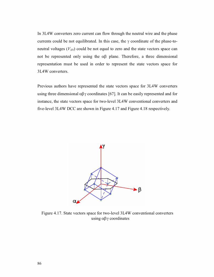
86
In 3L4W converters zero current can flow through the neutral wire and the phase
currents could be not equilibrated. In this case, the γ coordinate of the phase-to-
neutral voltages (VXN) could be not equal to zero and the state vectors space can
not be represented only using the αβ plane. Therefore, a three dimensional
representation must be used in order to represent the state vectors space for
3L4W converters.
Previous authors have represented the state vectors space for 3L4W converters
using three dimensional αβγ coordinates [67]. It can be easily represented and for
instance, the state vectors space for two-level 3L4W conventional converters and
five-level 3L4W DCC are shown in Figure 4.17 and Figure 4.18 respectively.
Figure 4.17. State vectors space for two-level 3L4W conventional converters using αβγ coordinates

87
Figure 4.18. State vectors space for five-level 3L4W DCC
In the three dimensional case, the reference voltage ( refur ) must be generated
carrying out a linear combination of the four nearest vectors. These nearest state
vectors form a volume (a tetrahedron) and therefore 3D SVPWM algorithms
have to find out the tetrahedron where the reference vector is pointing to. After
discovering the tetrahedron, the modulation algorithm knows the four nearest
vectors (they are the vertexes of the tetrahedron) to carry out the linear
combination of them in order to generate the reference vector averaged over a
sampling period. An example of the reference vector generation in a five-level
DCC is shown in Figure 4.19.

88
Figure 4.19. Reference vector generation using the four nearest vectors in a five-level 3L4W DCC
Using αβγ coordinates, the possible tetrahedrons that compose the state vectors
space have different shapes and volumes. Several volume shapes appear and it is
not easy to develop computationally efficient modulation algorithms to find out
the tetrahedron where the reference vector is pointing to. In spite of it, some
authors have developed 3D SVPWM algorithms using αβγ coordinates for 3L4W
topologies [67]. But these algorithms are complex and their computational cost is
important. This is the fundamental drawback of this type of 3D SVPWM
algorithms.

89
Therefore, it is necessary to change the representation way of the multilevel state
vectors space. This is the reason because abc coordinates are used by other
authors doing modulation algorithms more simple and more easily implemented
[70]. In order to reduce the 3D SVPWM computational cost, 3L4W converters
state vectors space can be represented using abc coordinates instead αβγ
coordinates. The state vectors space for two-level 3L4W conventional converters
is shown in Figure 4.20.
Figure 4.20. State vectors space for two-level 3L4W conventional converters using abc coordinates
It must be noticed that for 3L4W case, there are not redundant vectors because
the state vectors are located in different positions. The 3L4W converter state
vectors space increasing the number of levels can be done. For instance, the
three-level 3L4W converter state vectors space is shown in Figure 4.21.

90
Figure 4.21. Three-level 3L4W converter state vectors space using abc coordinates
Increasing the number of levels of the converter, the state vectors space for an N-
level 3L4W converter forms a cube in the 3D-space. This cube is formed by a
certain number of sub-cubes depending on the number of the levels of the
converter. Only one sub-cube for two-level converters, eight sub-cubes for three-
level converters, twenty-seven sub-cubes for four-level converters. In general,
(N-1)3 sub-cubes into the total cube, where N is the number of levels of the
multilevel converter.
Using abc coordinates, the modulation algorithm computational cost is lower
than using αβγ coordinates. In fact, abc coordinates divide the volume control in
cubes doing easier and faster the search for the four nearest vectors to the
reference vector. A fast and efficient generalized multilevel 3D SVPWM
algorithm was presented in [70]. It is based on a generalization of 3D SVPWM

91
presented in [66] and it is the basis of other developed multilevel 3D SVPWM
algorithms presented in this thesis.
Besides, using [70] the number of switching commutations and the number of
calculations to determine the switching sequence and the duty cycles are
minimized. In this generalized modulation algorithm, the N-level generalization
is done thanks to the reduction of the multilevel problem into a two levels one.
This basic 3D SVPWM algorithm is based on several steps:
Step 1: Calculate the coordinates of the sub-cube reference vertex where the
reference vector is found.
The multilevel control region is divided in several sub-cubes and the first step
of the modulation algorithm is to find the sub-cube where the reference vector is
pointing to. Considering this sub-cube using abc coordinates and changing the
origin coordinates to the nearest to (0,0,0) sub-cube vertex, the problem is
reduced to a two level case because the two level control region is one sub-cube.
For a certain reference vector in three-phase coordinates (uan, ubn, ucn), the integer
part of each component (a,b,c) is calculated with uan, ubn, ucn ∈ 0,..., 2(N-1).
a = integer (uan),
b = integer (ubn), (4.3)
c = integer (ucn),
The coordinates (a,b,c) are the coordinates origin corresponding to the reference
system of the sub-cube where the reference vector is pointing to. This sub-cube is
exactly equal as the two-level state vectors space case. So, the multilevel case is
reduced to a two levels case only calculating the factors a, b and c. This is shown
in Figure 4.22.

92
Figure 4.22. Sub-cube reference coordinates in generalized 3D SVPWM algorithms
Step 2: Divide the sub-cube in several tetrahedrons.
Once (a,b,c) coordinates are known, the algorithm calculates the four state
vectors corresponding to the four vertices of the tetrahedron into the selected
sub-cube where the reference vector is located. These vectors will generate the
reference vector.
The first option to divide the sub-cube was presented in [70]. Using this sub-
cube division, the tetrahedron where the reference vector is located is easily
found using comparisons with three 45º planes into the 3D space which define
the six tetrahedrons inside the sub-cube. These tetrahedrons are shown in Figure
4.23. In [70], the diagram flow to find out the nearest four vectors is shown and it
is important to notice that they are calculated using a maximum of three

93
comparisons for calculating the suitable tetrahedron. The modulation algorithm is
so easy due to the 45º planes dividing the sub-cube. This space division is named
SD45 in this work.
But other sub-cube divisions can be considered. 3D SVPWM algorithms look
for the best tetrahedron to generate the reference vector. The best solution is to
use the tetrahedron where all the distances between the reference vector and the
four state vectors are minimum. In fact, the ideal solution would be to increase
infinitely the number of levels of the converter doing that the reference vector is
always perfectly generated using only one state vector. So, minimizing the
distances between the reference vector and the state vectors, the ripple of the
resultant output signals will be minimized.
Other planes can be used to divide each sub-cube and in this thesis, new
division planes are presented. Four new planes are used to divide the sub-cube
volume and resulting tetrahedrons are shown in Figure 4.24. In this case, five
tetrahedrons compose the sub-cube volume where there is one central tetrahedron
and four external ones. Five is the minimum number of tetrahedrons to compose
the sub-cube. This fact is mathematically demonstrated in [1]. This new space
division is named SD1.

94
Figure 4.23. Sub-cube division using 45º planes (named SD45 space division). Six tetrahedrons compose the total sub-cube volume

95
a
c
b
000
111
101001
100
011
010 110
CASE 2
a
c
b
000
111
101001
100
011
010 110
CASE 1
a
c
b
000
111
101001
100
011
010 110
CASE 4
a
c
b
000
111
101001
100
011
010 110
CASE 3
a
c
b
000
111
101001
100
011
010 110
CASE 5
Figure 4.24. Sub-cube division using new planes (named SD1). Five tetrahedrons compose the total sub-cube volume

96
Using the same notation described in [70], the flow diagram to find out the
tetrahedron where the reference vector is pointing to using SD1 is shown in
Figure 4.25. Once the tetrahedron is found, the state vectors to be used and their
duty cycles can be determined using Table I.
Normalizedreference vector:
(uan, ubn, ucn)
ra+rb-rc < 0
a = integer (uan)b = integer (ubn)c = integer (ucn)
ra=uan-arb=ubn-brc=ucn-c
Yes No
Yes
Yes
No
No
ra-rb+rc < 0
Case 4ra+rb+rc > 2
Yes Nora-rb-rc > 0
Case 2 Case 5
Case 1
Case 3
Figure 4.25. Flow diagram to find out the tetrahedron where the reference vector is pointing to using space division SD1

97
More possible sub-cube divisions can be considered using SD1 but rotating
them 90º over b axis. The obtained tetrahedrons (named space division SD2) are
represented in Figure 4.26. In the same way that using previous 3D space
divisions, other flow diagram can be defined to find out the tetrahedron where
the reference vector is pointing to. The flow diagram for space division SD2 is
shown in Figure 4.27.
Step 3: Duty cycles calculation.
The reference vector is generated by a linear combination of four state vectors
determined in step 2. jinS is the phase i state located in position j in the switching
sequence and dj is the duty cycle j. The duty cycles calculation can be described
using the following matrix expression.
1 1 1
2 2 2
1 2 3 4 3 3 3
4 4 4
1
11
[ 1] [ ]11
an bn cn
an bn cna b c
an bn cn
an bn cn
S S SS S S
r r r d d d dS S SS S S
R D S D R S −
=
= → =i i (4.4)
Using these equations, the modulation algorithm can determine the duty
cycles. The final results using SD45, SD1 and SD2 are shown in TABLE 4.I,
TABLE 4.II and TABLE 4.III respectively. These tables summarize the
switching sequences and the duty cycles for all possible locations of the
reference vector inside the two-level sub-cube.

98
a
c
b
000
111
101001
100
011
010 110
CASE 9
a
c
b
000
111
101001
100
011
010 110
CASE 6
a
c
b
000
111
101001
100
011
010 110
CASE 7
a
c
b
000
111
101001
100
011
010 110
CASE 8
a
c
b
000
111
101001
100
011
010 110
CASE 10
Figure 4.26. Sub-cube division SD2. Five tetrahedrons compose the total sub-cube volume

99
Normalizedreference vector:
(uan, ubn, ucn)
-ra+rb+rc > 1
a = integer (uan)b = integer (ubn)c = integer (ucn)
ra=uan-arb=ubn-brc=ucn-c
Yes No
Yes
Yes
No
No
ra+rb-rc > 1
Case 7ra+rb+rc > 2
Yes Nora-rb-rc < 0
Case 9 Case 10
Case 6
Case 8
Figure 4.27. Flow diagram to find the tetrahedron where the reference vector is pointing to using space division SD2

100
TABLE 4.I
SPACE VECTORS SEQUENCE AND DUTY CYCLES DEPENDING ON
THE TETRAHEDRON CASE USING SPACE DIVISION SD45
Tetrahedron State vectors sequence Duty cycles
Case 1
(S1
an, S1bn, S1
cn) = (a, b, c) (S2
an, S2bn, S2
cn) = (a + 1, b, c) (S3
an, S3bn, S3
cn) = (a + 1, b, c + 1) (S4
an, S4bn, S4
cn) = (a + 1, b + 1, c + 1)
d1= 1 -ra, d2= ra - rc, d3= -rb + rc, d4= - rb,
Case 2
(S1an, S1
bn, S1cn) = (a, b, c)
(S2an, S2
bn, S2cn) = (a, b + 1, c)
(S3an, S3
bn, S3cn) = (a, b + 1, c + 1)
(S4an, S4
bn, S4cn) = (a + 1, b + 1, c + 1)
d1= 1 - rb, d2= rb - rc, d3= - ra + rc, d4= ra,
Case 3
(S1
an, S1bn, S1
cn) = (a, b, c) (S2
an, S2bn, S2
cn) = (a, b, c + 1) (S3
an, S3bn, S3
cn) = (a + 1, b, c + 1) (S4
an, S4bn, S4
cn) = (a + 1, b + 1, c + 1)
d1= 1 - rc, d2= - ra + rc, d3= ra - rb, d4= rb,
Case 4
(S1
an, S1bn, S1
cn) = (a, b, c) (S2
an, S2bn, S2
cn) = (a, b + 1, c) (S3
an, S3bn, S3
cn) = (a + 1, b + 1, c) (S4
an, S4bn, S4
cn) = (a + 1, b + 1, c + 1)
d1= 1 - rb, d2= - ra + rb, d3= ra - rc, d4= rc,
Case 5
(S1
an, S1bn, S1
cn) = (a, b, c) (S2
an, S2bn, S2
cn) = (a, b, c + 1) (S3
an, S3bn, S3
cn) = (a, b + 1, c + 1) (S4
an, S4bn, S4
cn) = (a + 1, b + 1, c + 1)
d1= 1- rc, d2= - rb + rc, d3= - ra + rb, d4= ra,
Case 6
(S1
an, S1bn, S1
cn) = (a, b, c) (S2
an, S2bn, S2
cn) = (a + 1, b, c) (S3
an, S3bn, S3
cn) = (a + 1, b + 1, c) (S4
an, S4bn, S4
cn) = (a + 1, b + 1, c + 1)
d1= 1- ra, d2= ra - rb, d3= rb – rc, d4= rc,

101
TABLE 4.II SPACE VECTORS SEQUENCE AND DUTY CYCLES DEPENDING ON
THE TETRAHEDRON CASE USING SPACE DIVISION SD1
Tetrahedron State vectors sequence Duty cycles
Case 1
(S1
an, S1bn, S1
cn) = (a, b, c + 1) (S2
an, S2bn, S2
cn) = (a + 1, b, c + 1) (S3
an, S3bn, S3
cn) = (a, b + 1, c + 1) (S4
an, S4bn, S4
cn) = (a, b, c)
d1= -ra-rb+rc, d2=1-d1-d3-d4, d3= rb, d4= 1-rc,
Case 2
(S1
an, S1bn, S1
cn) = (a + 1, b, c) (S2
an, S2bn, S2
cn) = (a + 1, b + 1, c) (S3
an, S3bn, S3
cn) = (a + 1, b, c + 1) (S4
an, S4bn, S4
cn) = (a, b, c)
d1= ra-rb-rc, d2= 1-d1-d3-d4, d3= rc, d4= 1- ra,
Case 3
(S1
an, S1bn, S1
cn) = (a + 1, b + 1, c + 1) (S2
an, S2bn, S2
cn) = (a + 1, b + 1, c) (S3
an, S3bn, S3
cn) = (a + 1, b, c + 1) (S4
an, S4bn, S4
cn) = (a, b + 1, c + 1)
d1= ra+rb+rc-2, d2= 1-rc, d3= 1-d1-d2-d4, d4= 1-ra,
Case 4
(S1
an, S1bn, S1
cn) = (a, b + 1, c) (S2
an, S2bn, S2
cn) = (a + 1, b + 1, c) (S3
an, S3bn, S3
cn) = (a, b + 1, c + 1) (S4
an, S4bn, S4
cn) = (a, b, c)
d1= -ra+rb-rc, d2= 1-d1-d3-d4, d3= rc, d4= 1-rb,
Case 5
(S1
an, S1bn, S1
cn) = (a + 1, b + 1, c) (S2
an, S2bn, S2
cn) = (a + 1, b, c + 1) (S3
an, S3bn, S3
cn) = (a, b + 1, c + 1) (S4
an, S4bn, S4
cn) = (a, b, c)
d1= 0.5 (ra+rb-rc), d2= 0.5 (ra-rb+rc), d3= 1-d1-d2-d4, d4=1-0.5 (ra+rb+rc),

102
TABLE 4.III SPACE VECTORS SEQUENCE AND DUTY CYCLES DEPENDING ON THE
TETRAHEDRON CASE USING SPACE DIVISION SD2
Tetrahedron State vectors sequence Duty cycles
Case 6
(S1
an, S1bn, S1
cn) = (a + 1, b, c + 1) (S2
an, S2bn, S2
cn) = (a + 1, b + 1, c + 1) (S3
an, S3bn, S3
cn) = (a, b, c + 1) (S4
an, S4bn, S4
cn) = (a + 1, b, c)
d1= ra-rb+rc-1, d2=1-d1-d3-d4, d3= 1-ra, d4= 1-rc,
Case 7
(S1
an, S1bn, S1
cn) = (a, b, c) (S2
an, S2bn, S2
cn) = (a, b + 1, c) (S3
an, S3bn, S3
cn) = (a, b, c + 1) (S4
an, S4bn, S4
cn) = (a + 1, b, c)
d1= 1-ra-rb-rc, d2= 1-d1-d3-d4, d3= rc, d4= ra,
Case 8
(S1
an, S1bn, S1
cn) = (a, b + 1, c + 1) (S2
an, S2bn, S2
cn) = (a + 1, b + 1, c + 1) (S3
an, S3bn, S3
cn) = (a, b + 1, c) (S4
an, S4bn, S4
cn) = (a, b, c + 1)
d1= -1-ra+rb+rc, d2= 1-d1-d3-d4, d3= 1-rc, d4= 1-rb,
Case 9
(S1
an, S1bn, S1
cn) = (a + 1, b + 1, c) (S2
an, S2bn, S2
cn) = (a + 1, b + 1, c + 1) (S3
an, S3bn, S3
cn) = (a, b + 1, c) (S4
an, S4bn, S4
cn) = (a + 1, b, c)
d1= -1+ra+rb-rc, d2= rc, d3= 1-ra, d4= 1-d1-d2-d3,
Case 10
(S1
an, S1bn, S1
cn) = (a + 1, b + 1, c + 1) (S2
an, S2bn, S2
cn) = (a, b + 1, c) (S3
an, S3bn, S3
cn) = (a, b, c + 1) (S4
an, S4bn, S4
cn) = (a + 1, b, c)
d1=0.5(-1+ra+rb+rc), d2=0.5(1-ra+rb-rc), d3=0.5(1-ra-rb+rc), d4=1-d1-d2-d3,

103
In order to compare SD45 and SD1 space divisions, the distances between the
reference vector and the four state vectors that compose the tetrahedron where
the reference vector is pointing to can be determined. These distances are named
x1, x2, x3, and x4. In Figure 4.28, the distances xi using SD45 and SD1 are shown.
Figure 4.28. Generation of the reference voltage using the four nearest state vectors using SD45 (a) and SD1 (b). The distances between the state vectors
and the reference vector are different
Depending on the used space division, the reference vector is generated using
different state vectors. Mathematically, the reference vector is correctly
generated using any space division but the distances xi change and consequently
the ripple of the output signals also changes. The output current ripple is related
to the value of the distances xi. If these distances decrease, it means that the
reference vector is generated with nearer state vectors and therefore the
instantaneous error due to each state vector is lower. A merit figure can be
defined in order to show xi distances in each case and what is the best solution
depending on the reference vector location. This merit figure is defined as:

104
1 2 3 4
1 1 1 1
1 11000 1000 1...4i i
Fx x x x
where if for ix x
= + + +
> → = = (4.5)
In order to pick out what is the best sub-cube division depending on the reference
vector location inside the two-level sub-cube, F functions for both space
divisions are calculated (FSD45 and FSD1). Finally, it is defined the function FT as
the difference of FSD1 and FSD45.
1 45T SD SDF F F= − (4.6)
FT can be determined for all possible locations of the reference vector in the sub-
cube. In the control regions where FT is lower than zero, SD45 appears as the
better solution. On the other hand, in the control regions where FT is greater than
zero, SD1 improves the ripple behaviour. In Figure 4.29, FT function is
represented for several values of b coordinate in two-level sub-cube. It is clear
that inside the central tetrahedron defined by SD1, SD45 improves FT. However,
in the outer parts of this central tetrahedron, SD1 improves the FT function. So, if
the reference vector is located into the central tetrahedron, the best solution is to
use SD45 space division and if the reference vector is outside central tetrahedron,
it is better to use SD1 space division.

105
Figure 4.29. Merit figure FT for several b coordinate values between 0 and 1. If FT is
positive or negative, the distances between the reference vector and the state vectors are
smaller using SD1 or SD45 respectively
Simulations have been carried out to show the SD1 performance. The simulated
system is a four-leg four-wire three-level diode clamped converter connected to
an RL load. The DC-Link voltage is equal to 1600 V, L=5 mH, R=22 Ω and the
switching frequency is 5 kHz. The reference is a pure sinusoidal waveform with
modulation index equal to 0.6875. Simulation results using SD45 and SD1 are
shown in Figure 4.30 and Figure 4.31 respectively. It is clear that undesired and
unexpected ripple effects in the output phase currents using SD1 appear.

106
Figure 4.30. Output phase currents using SD45 for a three-level 4L4W DCC considering VDC=1600V, L=5mH, R=22 Ω and the modulation index
m=0.6875. The reference voltage is a pure sinusoidal waveform and the switching frequency is 5 kHz
Figure 4.31. Output phase currents using SD1 for a three-level 4L4W DCC considering VDC=1600V, L=5mH, R=22 Ω and the modulation index
m=0.6875. The reference voltage is a pure sinusoidal waveform and the switching frequency is 5 kHz
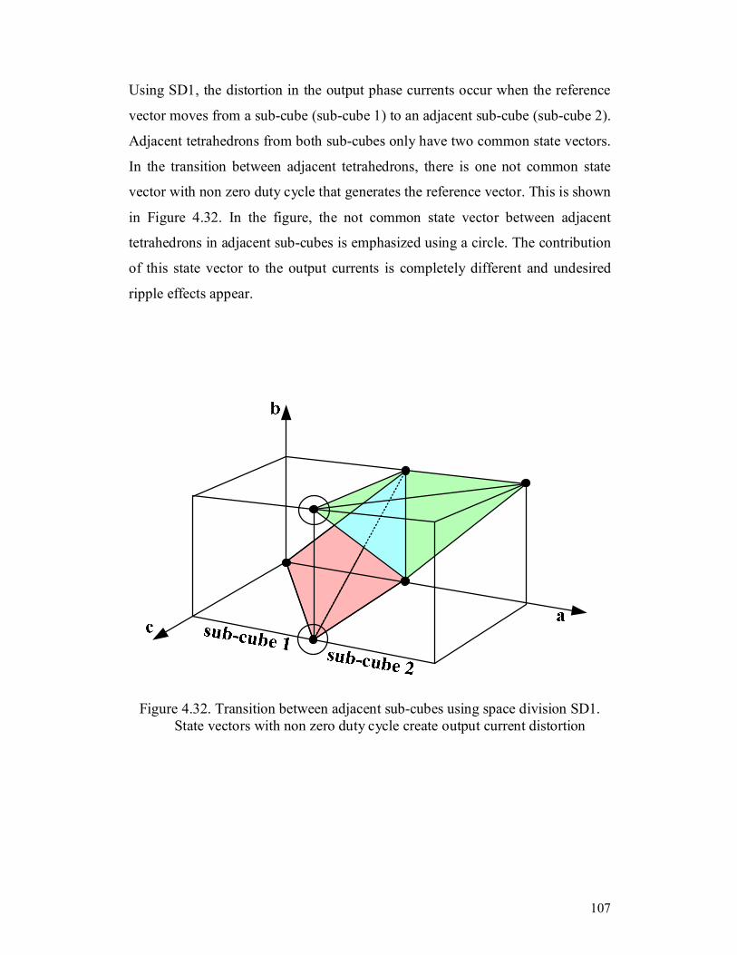
107
Using SD1, the distortion in the output phase currents occur when the reference
vector moves from a sub-cube (sub-cube 1) to an adjacent sub-cube (sub-cube 2).
Adjacent tetrahedrons from both sub-cubes only have two common state vectors.
In the transition between adjacent tetrahedrons, there is one not common state
vector with non zero duty cycle that generates the reference vector. This is shown
in Figure 4.32. In the figure, the not common state vector between adjacent
tetrahedrons in adjacent sub-cubes is emphasized using a circle. The contribution
of this state vector to the output currents is completely different and undesired
ripple effects appear.
Figure 4.32. Transition between adjacent sub-cubes using space division SD1. State vectors with non zero duty cycle create output current distortion

108
In order to avoid the presence of not common state vectors, adjacent sub-cubes in
the total control region are divided using SD1 and SD2 alternately. Using this
configuration in the control region, adjacent tetrahedrons from adjacent sub-
cubes have three common state vectors and in the transition instant, the fourth
state vector has zero duty cycle. So, the movement between adjacent sub-cubes is
done avoiding the presence of state vectors with non negligible duty cycles. This
space division is named SD12 and is represented in Figure 4.33.
Figure 4.33. Adjacent sub-cubes in the total control region divided using SD1 and SD2 alternately (named SD12 space division)
Considering the combination of the SD1 and SD2 control region division, the
same simulations can be carried out. In Figure 4.34, simulation output phase
currents results using SD12 space division are shown. It can be seen that the
obtained results are very similar.

109
Figure 4.34. Output phase currents using SD12 space division generating a pure sinusoidal reference for a three level four-leg four-wire diode clamped
converter considering VDC=1600V, L=5mH, R=22Ω and the modulation index m=0.6875. The reference voltage is a pure sinusoidal waveform and the
switching frequency is 5 kHz
As the obtained phase current results are similar at first sight, total harmonic
distortion (THD) values are calculated using SD45 and SD12. THD using SD45
and SD12 space division are represented in Figure 4.35 and Figure 4.36
respectively showing that both space divisions achieve similar THD contents.
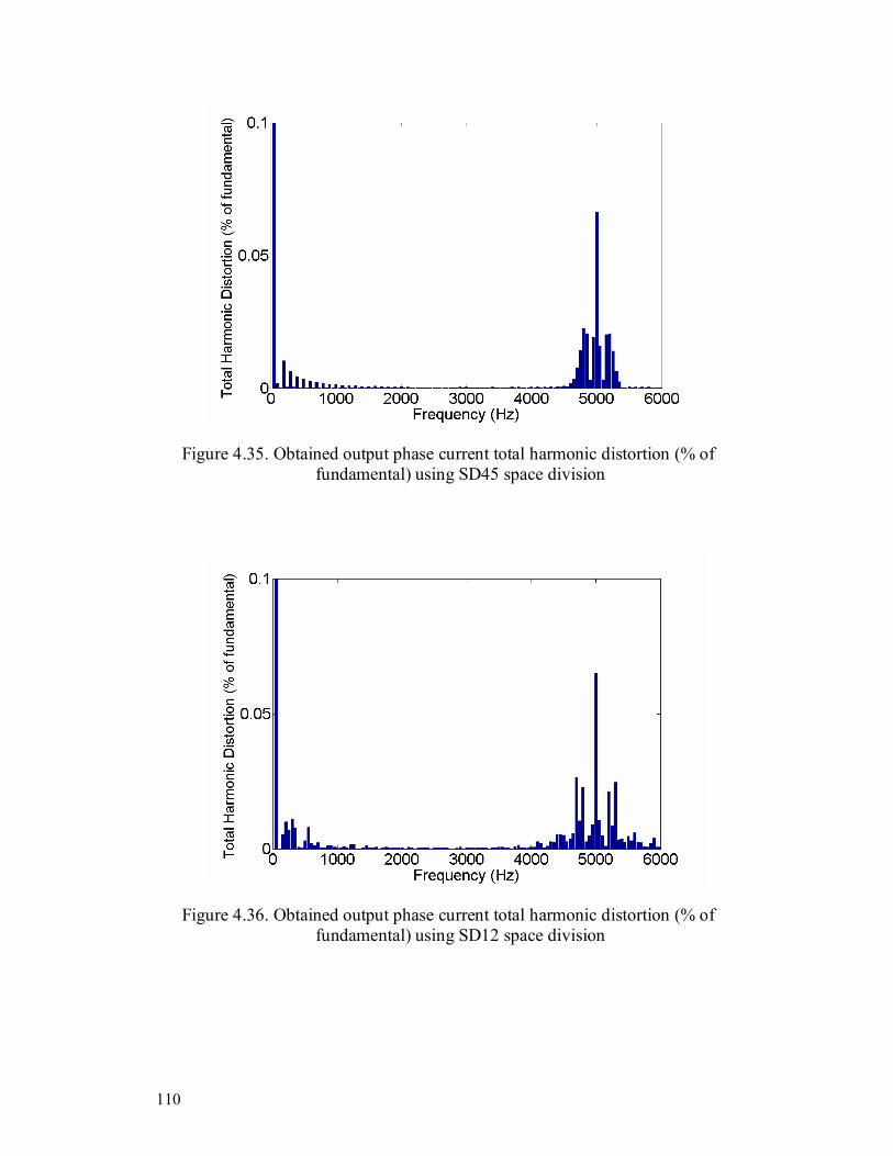
110
Figure 4.35. Obtained output phase current total harmonic distortion (% of fundamental) using SD45 space division
Figure 4.36. Obtained output phase current total harmonic distortion (% of fundamental) using SD12 space division

111
Three dimensional generalized space vector modulation algorithms are discussed
in this work. Two new space divisions and its related multilevel modulation
algorithms are shown. Finally, the combination of two different space divisions is
used to avoid undesired output phase current ripple effects. A comparison
between previous 3D modulation algorithm and the proposed algorithms is done.
The presented modulation algorithms calculate the state vectors and the duty
cycles without using angles, trigonometric functions or look-up tables. The
computational cost of the proposed method is very low, is always the same and is
independent of the number of levels of the converter. In general, the presented
algorithms are useful in systems with or without neutral, unbalanced load, and
harmonics generation.
4.3.3 Four-leg four-wire converters (4L4W)
Converters connecting the neutral point of the load to a converter phase are
named four-leg four-wire systems (4L4W systems) and they were presented in
chapter 2. A 4L4W two-level conventional converter is shown in Figure 4.37.
Figure 4.37. 4L4W two-level conventional converter

112
It can be seen that 4L4W multilevel converter state vectors space forms a
dodecahedron in the 3D-space [67][68][71]. This dodecahedron can be
decomposed into several sub-cubes, and each one can be divided in different
tetrahedrons that generate the total volume of each sub-cube. The 3D-
dodecaedron containing the state vectors which generate the reference vector in
4L4W three-level converter is shown in Figure 4.38. As another example, a
4L4W five-level converter is illustrated in Figure 4.39.
Figure 4.38. Generalized 3D state vectors space for 4L4W three-level converter
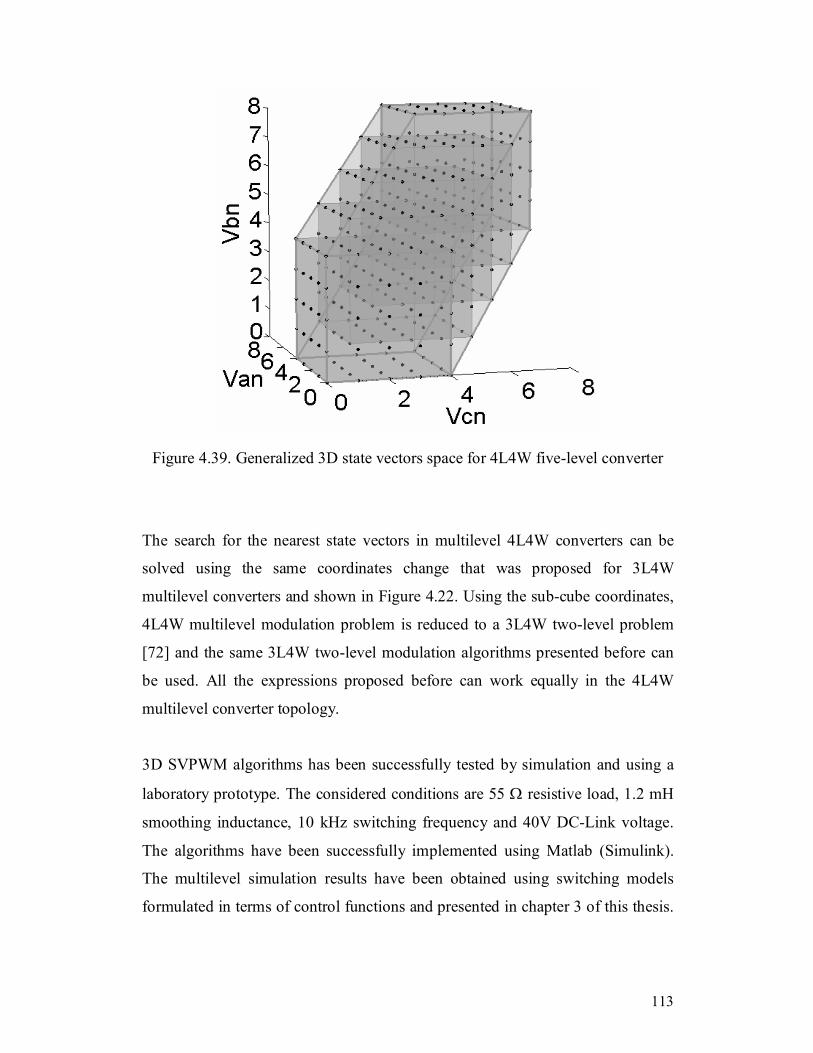
113
Figure 4.39. Generalized 3D state vectors space for 4L4W five-level converter
The search for the nearest state vectors in multilevel 4L4W converters can be
solved using the same coordinates change that was proposed for 3L4W
multilevel converters and shown in Figure 4.22. Using the sub-cube coordinates,
4L4W multilevel modulation problem is reduced to a 3L4W two-level problem
[72] and the same 3L4W two-level modulation algorithms presented before can
be used. All the expressions proposed before can work equally in the 4L4W
multilevel converter topology.
3D SVPWM algorithms has been successfully tested by simulation and using a
laboratory prototype. The considered conditions are 55 Ω resistive load, 1.2 mH
smoothing inductance, 10 kHz switching frequency and 40V DC-Link voltage.
The algorithms have been successfully implemented using Matlab (Simulink).
The multilevel simulation results have been obtained using switching models
formulated in terms of control functions and presented in chapter 3 of this thesis.

114
The experimental results have been obtained with a real prototype using a
TMS320VC33 DSP microprocessor.
In order to test the proposed technique an unbalanced voltage reference
composed of a fundamental component with 20V amplitude, 20% of zero
sequence and 20% inverse sequence has been used. Voltage references for each
phase are represented in Figure 4.40. Voltage references of each phase are
illustrated in Figure 4.41.a, Figure 4.42.a and Figure 4.43.a. The simulation
results are shown in Figure 4.41.b, Figure 4.42.b and Figure 4.43.b and the
experimental results are shown in Figure 4.41.c, Figure 4.42.c and Figure 4.43.c.
Figure 4.40. Voltage reference for each phase composed of a fundamental component with 20V amplitude, 20% of zero sequence and 20% inverse
sequence

115
Figure 4.41. Voltage for phase a, composed of a fundamental component with 20V amplitude, 20% of zero sequence and 20% inverse sequence
Figure 4.42. Voltage for phase b, composed of a fundamental component with 20V amplitude, 20% of zero sequence and 20% inverse sequence

116
Figure 4.43. Voltage for phase c, composed of a fundamental component with 20V amplitude, 20% of zero sequence and 20% inverse sequence
Another reference vector containing a fundamental component with 40
3V
amplitude and 120% of the third harmonic has been proved for the sake of
clarity. Voltage reference for each phase is illustrated in Figure 4.44. The voltage
reference, the simulated results and the experimental results of this experiment
are shown in Figure 4.45. Clearly, the voltage signal across the phase resistor
follows the input reference signal. These results show the good performance of
the proposed algorithm.

117
Figure 4.44. Voltage reference composed of a fundamental component with 40
3V amplitude and 120% of the third harmonic
Figure 4.45. Voltage signals with 403
V amplitude and 120% of the third
harmonic

118
Chapter 5
Solving the Balancing of the Capacitors Voltage in Multilevel Converters 5.1 Introduction
Multilevel converters present several advantages compared to classical two-level
converters [5][6]. They improve the harmonic content of the output signals and
they accept a power increase in the DC-link due to its voltage can be shared
between more transistors. As disadvantages, the multilevel converters increase
the control and the implementation complexity. Recently the control complexity
has been reduced thanks to the use of new and powerful microprocessor systems
[73]-[75]; hence the balance of the DC capacitors voltage is one of the most
important drawbacks of this type of converter topologies. In this chapter, control
strategies to carry out the balance the DC capacitors voltage for multilevel

119
converters are presented. These strategies use the well known technique based on
choosing the correct redundant vector using Space Vector Modulation algorithms
in order to reduce the voltage unbalance [77]-[89]. It is important to notice that
the proposed methods are completely generalized and due to it, they are
independent of the load and independent of the number of levels of the converter.
Some simulation and experimental results show the obtained balance using the
proposed techniques.
If any unbalance in the DC capacitors voltage appears, the output phase voltages
have distortion and the harmonic content of the output signals decreases its
quality. In fact, if the switching control is not be made carefully and a control
algorithm is not carried out, the problem immediately appears and the DC
capacitors voltage will be unbalanced.
5.2 Quasi-solution of the voltage balancing
problem
Redundant vectors using SVPWM techniques can be used to achieve DC
capacitors voltage balance [77]-[89]. These vectors have the same phase-to-
neutral output voltages but their effect in the DC capacitors voltage is completely
different. This chapter shows that the balancing problem of the DC capacitors
voltage in multilevel converters topologies can be solved using the redundant
vectors. However, the increasing complexity with the number of levels makes
very difficult to choose the best redundant vector to control the voltage
unbalance. In fact, sometimes this choosing is impossible due to there are cases
where all the possible redundant vectors do not decrease the unbalance.

120
It should be noticed that increasing the number of levels, the number of
redundant vectors in multilevel state vectors space increases exponentially. In
fact, the number of state vectors for N-level 3L3W DCC converter is N3. The
number of redundant vectors (NRV) for N-level 3L3W DCC can be determined
using the expression (5.1). The evolution of the total number of state vectors and
redundant vectors is shown in Figure 5.1.
2
16 ( )
N
iNRV N i N i
−
=
= + −∑ (5.1)
Figure 5.1. Number of redundant vectors depending on the number of levels in DCC topology

121
Depending on the multilevel converter topology, the DC capacitor voltages must
take different values. For instance, in multilevel DCC topology, all DC-link
capacitors must equally share the DC-link voltage [20]. Three-level DCC
topology is represented in Figure 5.2 showing that capacitors C1 and C2 share the
DC-Link voltage. For N-level DCC case, ∆VCi can be defined as the unbalance of
the capacitor Ci as follows:
1DC
Ci CiVV VN
∆ = −− (5.2)
Figure 5.2. Three-level DCC topology. DC-Link voltage is equally shared between capacitors C1 and C2

122
On the other hand, in multilevel FCC topology, each flying capacitor voltage
value is different [26]. For instance, a four-cell conventional FCC using OFBCS
flying capacitor voltages ratio is represented in Figure 5.3 showing the flying
capacitor voltages values. For M-cell OFBCS FCC, ∆VCi can be defined as the
unbalance of the flying capacitor Ci as follows:
( )Ci Ci DC
M iV V VM
−∆ = − (5.3)
Figure 5.3. Four-cell FCC topology showing the different flying capacitors voltage values using OFBCS flying capacitor voltages ratio

123
High number of publications has been focused on the development of control
strategies to solve the voltage unbalance for multilevel converters [77]-[91]. As it
was said in chapter 4, depending on the multilevel converter topology, different
redundant vectors appear in the converter state vectors space. Previous authors
have proposed control algorithms based on choosing the best redundant vector to
control the DC capacitors voltage [89]-[91]. In this thesis, generalized algorithms
using the redundant vectors concept are presented for any number of levels in the
converter. The proposed control algorithms are based on the calculation of the
currents that flow through DC capacitors (iSi) depending on instantaneous state
vector applied to the multilevel converter. These algorithms could seem very
complex at first sight but it will be shown that they are very fast and simple. All
the calculations are completely generalized and they do not imply complex
operations or look-up tables. Generalized expressions for N-level converters have
been developed. An important contribution is the performance of a systematic
method to study any multilevel converter topology to develop control algorithms
for future converter topologies.
5.3 Voltage balancing problem depending
on the multilevel converter topology The balancing control algorithms proposed in this thesis are based on the
determination of the currents that flow through DC capacitors that can suffer the
voltage unbalance. In general, these currents depend on the state vector applied
to the converter. In next points, a deep study of the calculation of these currents
depending on the converter topology is presented. The knowledge of the
expressions of these currents and the capacitors voltage unbalance are the base of

124
the balancing control algorithms. In this thesis it is assumed that the DC-Link
voltage is constant thanks to an external voltage source (controlled rectifier,
external independent voltage source…).
As it was said before it was defined ∆VCi as the unbalance of capacitor Ci
determined by the difference between the real capacitor voltage and the desired
capacitor voltage (see expressions (5.2(5.3). Depending on the converter
topology, the voltage unbalance expression is different. Using the signal criteria
defined in Figure 5.4, the control strategy to achieve DC capacitors voltage
balance can be easily developed. If current iSi sign and unbalance ∆VCi sign are
not equal, the unbalance will decrease. So, the control algorithms should choose
the redundant vector that fulfils this property.
Ci
Cj
VDC+-
isi
isj
VCi
VCj
Figure 5.4. Signs criterion used in the control strategies

125
Sometimes the perfect redundant vector choosing to reduce the voltage
unbalance is impossible due to there are cases where all the possible
redundant vectors do not decrease the unbalance. Several balancing control
algorithms were tested depending on the redundant vectors choosing
criterion. The balancing control algorithms studied were:
1. To find the most unbalanced capacitor and to choose the redundant vector
that puts the best current through this capacitor.
2. To find the highest current in absolute value and to choose the redundant
vector that achieves the best capacitor configuration.
3. To find the redundant vector that achieves the best capacitor configuration
to minimize the negative effects in the voltage balance.
4. To find the redundant vector that achieves the best capacitor configuration
to maximize the positive effects in the voltage balance.
5. To find the redundant vector that achieves the best capacitor configuration
taking into account the negative and the positive effects in the capacitors
voltages.
Studying these balancing control algorithms by simulations using
Matlab/Simulink® models presented in chapter 3 it can be concluded that:
• Controlling multilevel converters with algorithms number one and four do
not reach good results. The system turns unstable.
• Controlling multilevel converters with the other balancing algorithms
reaches good results achieving the stability but only under some
conditions.
Finally, the balancing control algorithm number five was chosen because it takes
into account all the system and all the control variables. For N-level converters,
the balancing control algorithm finds the best redundant vector in the simplest
way. The algorithm chooses the state vectors that minimize the sum of the

126
products of ∆VCi and iSi with i=1,.,N-1. In this way, the control algorithm assures
that the final chosen redundant vectors maximize, in average, the tendency to the
voltage balance of all DC capacitors. In fact, this control method really implies a
minimization of the electrical energy stored in the chain of DC capacitors [91].
The minimization of this parameter directly means the minimization of the
averaged unbalance of DC capacitors. But in general, increasing the number of
levels and considering N-level, it is not always possible to find a redundant
vector that tends to equilibrate all the DC capacitors voltage.
It is important to notice that all the necessary expressions to be applied in the
control algorithms are very simple and they can be easily implemented in a
microprocessor system being the control strategy computational cost very low.
Besides, the control method is completely generalized and due to it, it is
independent of the load type and it is independent of the number of levels of the
converter.
5.3.1 Diode-Clamped Converter Topology Using this converter topology and assuming that SVPWM algorithm applies a
specific state vector to the converter, the DC-link capacitors are divided in
several blocks. Each block is composed by several capacitors in series.
Considering that all capacitors have the same capacitance value C, they can be
associated forming different capacitors C/ki where ki is the number of capacitors
in series in each block. The sum of ki is the total number of DC-link capacitors
that is equal to N-1 in an N-level DCC topology. This concept will be shown
clearly in the next points.

127
1
4 31
5 4
m
ii
for wire convertersk N with m
for wire converters=
−= − = −
∑ (5.4)
It can be assumed that VDC is approximately constant due to the converter is
usually connected to a device, e.g. a rectifier, that supports the total DC-link
voltage. Supposing that total DC-link voltage is constant, it is a fact that there is a
relation between the currents through the DC-link capacitors (iSi).
1
1
10
m
DC Sii
m mS
i Sii i i
V V
dCdt
dVC k idt
=
= =
=
↓
= =
∑
∑ ∑
(5.5)
∆VCi is the unbalance of capacitor Ci and the expression was presented in
expression (5.2). Using the signal criteria defined in Figure 5.4, the control
strategy to achieve the balance of the DC-Link voltage can be easily developed.
If the sign of the current iSi and the sign of ∆VCi are not equal, the unbalance will
decrease.

128
5.3.1.1 N-level three-leg three-wire Diode-Clamped (3L3W DCC)
Topology
The control algorithm for the DC-Link capacitor voltages balancing needs to find
out the currents that flow through those DC capacitors. As it was said before, ki is
defined as the number of DC capacitors connected in series applying a specific
state vector to the converter and therefore, it takes values between 0 and N-1 for
N-level DCC.
In N-level 3L3W DCC, each phase load is connected to some DC-Link point
applying the state vector imposed by the SVPWM algorithm. These connections
depending on the applied state vector can be represented in a very simple way
considering ideal power switching devices and assuming that all capacitors have
the same capacitance value. In N-level 3L3W DCC only two different cases must
be studied to determine iSi currents for all possible redundant state vectors.
Current iP3 is the phase current flowing through the phase connected to the
highest level, iP1 is the phase current flowing through the phase connected to the
lowest level and iP2 is the phase current flowing through the phase connected to a
medium level.
I. State vectors where k2>0, k3>0 and k4 and k1 can not be simultaneously
zero
This configuration is the generalized version of a redundant vector where the
phases of the load are connected to different points of the DC-Link. In fact, if
k1=0 and k4=0 simultaneously, the state vector is not redundant. This
configuration is shown in Figure 5.5.

129
Figure 5.5. 3L-3W DCC with case 1 configuration (k2>0, k3>0 and k4 and k1 can
not be simultaneously zero)
Analyzing this case, iSi expressions can be determined as follows.
+ + + =
↓
+ = − −+ +
= = → =−
+ + − += − =
−+ + − + + −
= + =−
4 3 2 1
4 4 1 1 2 2 3 3
2 2 2 3 34 1
2 3 3 2 23 3
2 3 3 2 22 1
( )1
( 1 )1
( 1 ) ( 1 )1
C C C C DC
S S S S
P PS S S S
P PS S P
P PS S P
V V V V VdCdt
k i k i k i k ik i k k ii i i i
Nk k N i k ii i i
Nk k N i k N ii i i
N
(5.6)

130
II. State vectors where k1 and k4 are not simultaneously equal to zero and
k3=0, k2 >0 or k2 =0, k3 >0
Figure 5.6. 3L-3W DCC with case 2 configuration (k1 and k4 are not simultaneously equal to zero and k3=0, k2 >0 or k2 =0, k3 >0)
Analyzing this case, iSi expressions can be determined as follows.
+ + = → + = −
= = → =−
+= − = −
−
4 2 1 4 4 1 1 2 2
2 24 1
1 42 2 2
1( )
1
C C C DC S S S
PS S S S
S S P P
V V V V k i k i k ik ii i i iN
k ki i i iN
(5.7)

131
All the redundant state vectors can be studied changing the values of ki factors
and recalculating iSi values. After determining the currents through the DC-link
capacitors associated to each redundant state vector, the balancing control
algorithm must choose carefully the best redundant state vector in order to
equilibrate the DC-link capacitors voltage.
5.3.1.2 N-level four-leg four-wire Diode-Clamped (4L4W DCC)
Topology
As it was said before, it can be assumed that VDC is approximately constant due
to the converter is usually connected to a device, e.g. a rectifier, that supports the
total DC-link voltage. Supposing it, the relation between the currents through the
DC-link capacitors (iSi) can be rewritten.
1 2 3 4 5
1 2 3 4 5
1 1 2 2 3 3 4 4 5 5
0
0
DC C C C C C
C C C C C
S S S S S
V V V V V VdCdt
dV dV dV dV dVC C C C Cdt dt dt dt dt
k i k i k i k i k i
= + + + +
↓
= + + + +
= + + + +
(5.8)
In order to generalize the study and to know the way to choose the best redundant
vector to carry out the balance of the DC-link voltage, all the possibilities are
studied. Several possible switching configurations appear depending on the
position of the connection of the fourth leg. All the cases can be summarized in
132
Figure 5.7 (case 1), Figure 5.8 (case 2), Figure 5.9 (case 3) and Figure 5.10 (case
4). As it was said for 3L3W DCC case, current iP3 is the phase current flowing
through the phase connected to the highest level, iP1 is the phase current flowing
through the phase connected to the lowest level and iP2 is the phase current
flowing through the phase connected to a medium level. Besides, iN is the current
that flows through the phase connected to neutral point of the load (the fourth
leg).

133
Figure 5.7. First case of possible switching state configuration of multilevel 4L4W DCC
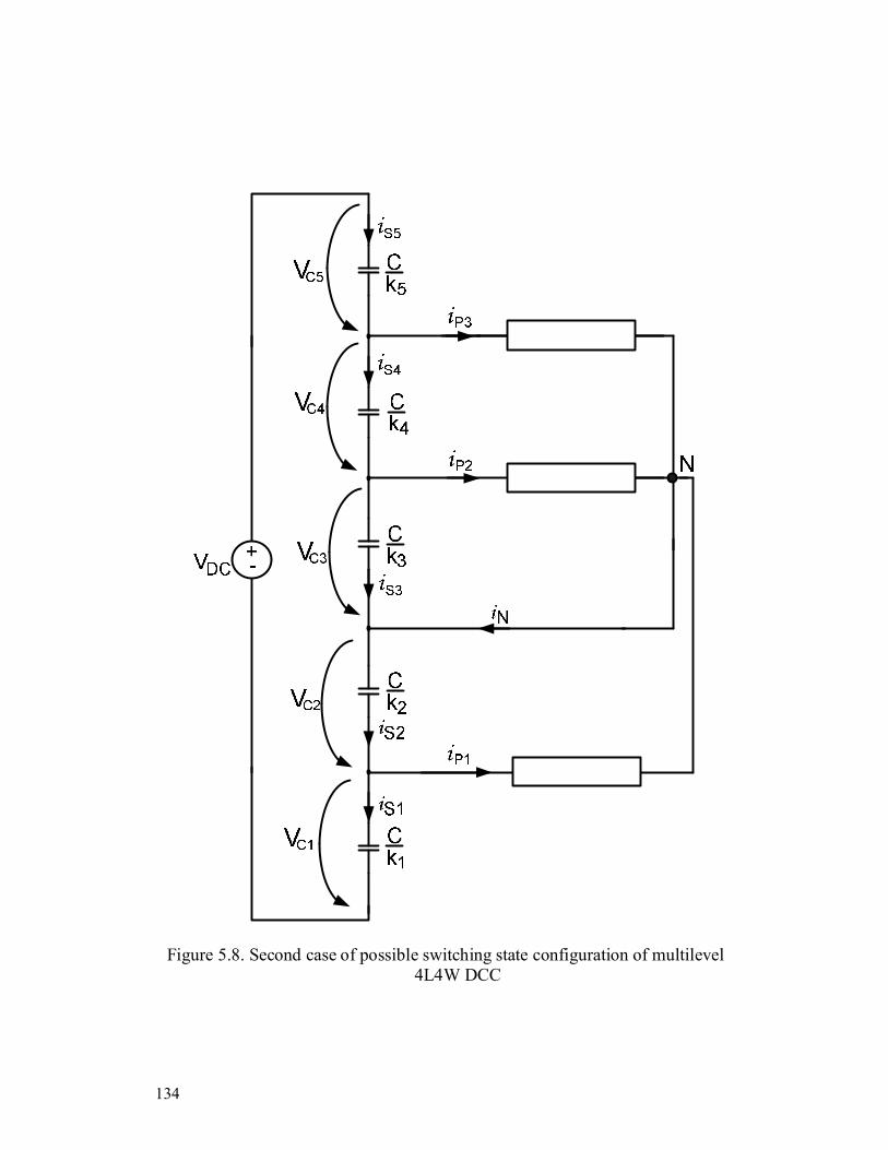
134
Figure 5.8. Second case of possible switching state configuration of multilevel 4L4W DCC

135
Figure 5.9. Third case of possible switching state configuration of multilevel 4L4W DCC

136
Figure 5.10. Fourth case of possible switching state configuration of multilevel 4L4W DCC

137
All the cases can be easily solved and iSi results can be summarized as follows.
1 2 1 2 3 2 2 3 4 3
2 2 1 1 4 5 2 1 5 3
3 2 1 1 4 5 2 1 5 3
4 2 1 2 3 2 1 5 3
1 2 1 3 2
1:
1 [ ( ) ( ) ]11 [( 1 ) ( ) ( ) ]
11 [ ( ) ( ) ]
11 [ ( ) ( ) ]
1
2:
1 [ (1
S P P P
S P P P
S P P P
S P P P
S P P
Case
i k i k k i k k k iN
i N k i k k k i k k iN
i k i k k k i k k iN
i k i k k i k k iN
Case
i k i k i kN
= + + + + +−
= − − − + + + + +−
= − + + − +−
= + + − +−
= − + +− 3 4 3
2 2 1 3 2 3 4 3
3 2 1 3 2 1 2 5 3
4 2 1 3 2 1 2 5 3
1 2 3 1 3 2 4 3
2 1 4 5 1 3 2 4 3
) ]
1 [( 1 ) ( ) ]11 [ ( 1 ) ( ) ]
11 [ ( ) ]
1
3:
1 [ ( ) ]1
1 [( ) ]1
P
S P P P
S P P P
S P P P
S P P P
S P P P
k i
i N k i k i k k iN
i k i N k i k k k iN
i k i k i k k k iN
Case
i k k i k i k iN
i k k k i k i k iN
i
+
= − − + + +−
= − + − − + + +−
= − + − + +−
= − + − +−
= + + − +−
3 1 4 5 1 3 2 4 3
4 2 3 1 3 2 4 3
1 2 3 4 1 3 4 2 4 3
2 1 5 1 3 4 2 4 3
3 1 5 1 1 2 5 2 4
1 [( ) ( 1 ) ]11 [( ) ( 1 ) ]
1
4:
1 [( ) ( ) ]1
1 [( ) ( ) ]1
1 [( ) ( )1
S P P P
S P P P
S P P P
S P P P
S P P
k k k i N k i k iN
i k k i k i N k iN
Case
i k k k i k k i k iN
i k k i k k i k iN
i k k i k k k i k iN
= + + + − − +−
= − + + + − −−
= − + + + + +−
= + − + −−
= + + + + −− 3
4 1 5 1 1 2 5 2 4 3
]
1 [( ) ( ) ( 1 ) ]1
P
S P P Pi k k i k k k i N k iN
= + + + + + − −−
(5.9)

138
It can be studied, for instance, the three-level case. In this case, several double
and triple redundant state vectors appear. These redundant state vectors can be
summarized in TABLE 5.I. All the possible redundant vectors can be classified
in the four cases explained before.
Using the expressions proposed in TABLE 5.I, iSi currents can be easily
calculated depending on the selected redundant state vector. In the three-level
case, there are only two DC-Link capacitors; hence iS1 and iS2 can be determined.
It can be remembered that using the expression (5.8) it must be fulfilled the
expression iS2 =-iS1. As it was presented in (5.2), ∆VCi in the three-level case is:
2DC
Ci CiVV V∆ = − (5.10)
Considering three-level 4L4W DCC, in all the possible cases, the current through
capacitor C1 (iS1) in the redundant state vectors has opposite signs. This result is
very important because in three-level case, the control algorithm can always
select the sense of currents flowing through DC-link capacitors C1 and C2
choosing the redundant vector that tends to equilibrate the DC-link voltage.

139
State vector
Redundant vectors Case
000|0 111|1
222|2 -
000|1 111|2 4
001|0 112|1 1
010|0 121|1 1
100|0 211|1 1
001|1 112|2 4
010|1 121|2 4
100|1 211|2 4
011|0 122|1 1
101|0 212|1 1
110|0 221|1 1
011|1 122|2 4
101|1 212|2 4
110|1 221|2 4
111|0 222|1 1
TABLE 5.I. Each redundant vector in 4L4W DCC can be studied using one of the four simplified cases presented in Figure 5.7, Figure 5.8, Figure 5.9 and
Figure 5.10

140
Simulation experiments have been carried out considering three-level 4L4W
DCC topology connected to an RL load composed by R = 22Ω, L = 5mH,
fsw(switching frequency)=5kHz, C1=C2=500µF and VDC(DC-Link voltage)
=1600V. The reference waveform is a sinusoidal signal with modulation index
m=0.99 and 80% third harmonic. The good performance of the control algorithm
is shown in Figure 5.11 where the one DC-Link capacitor voltage and the output
phase currents are shown..
Figure 5.11. DC-Link Capacitor C1 voltage and output phase currents showing the good performance of the balancing control algorithm for three-level
4L4W DCC

141
In order to show the good performance of the control algorithm, some simulation
results with higher number of levels are shown. It can be considered the same
experiment described in the three-level case (see Figure 5.11) but using a five-
level converter and assuming that the modulation index is equal to 0.56. An
initial unbalance in the DC-link capacitors voltages is applied to show the
unbalance dynamics using the control algorithm. Therefore the simulation
experiment has been carried out considering five-level 4L4W DCC topology
connected to an RL load composed by R=22Ω, L=5mH, fsw (switching
frequency)=5 kHz, C1=C2=500 µF and VDC (DC-Link voltage)=1600V. The
reference waveform is a sinusoidal signal with modulation index m=0.56 and
80% third harmonic. Using five-level DCC four capacitors compose the DC-link
and their desired voltages are VDC/4 that is 400 volts in this case. In this
simulation, initially, VC1=470v, VC2=360v, VC3=370v and VC4=400v. In Figure
5.12 simulation results of the DC-link voltages are represented.
Figure 5.12. DC-link Capacitors voltage showing the good performance of the balancing control algorithm starting with a initial unbalance using a five-level
4L4W DCC

142
A 50KW real prototype three level 4L4W-DCC was developed in Norwegian
University of Science and Technology (NTNU) in Trondheim (Norway) in order
to test the proposed balancing control algorithm. The control hardware is
composed by TMS320F2812 microprocessor system and virtex XCV400BG432
FPGA. The DSP is responsible for the control algorithm and the FPGA makes the
switching of the transistors implementing the duty cycles making the system more
versatile and efficient [92][93]. The total DC-Link capacitors value is C=3300µF.
The prototype is shown in Figure 5.13.
Figure 5.13. 50 kW real prototype three-level 4L4W DCC developed in Norwegian University of Science and Technology (Trondheim, Norway)

143
Several experiments were carried out to test the converter and the 4L4W DCC
balancing control algorithm. All the expressions presented before can be applied
directly only doing the factor N (number of levels of the converter) equal to 3. In
the experiments, the converter is connected to a three-phase RL load where
R=23.5Ω and L=1.4mH. The total DC-Link voltage is 80 volts. It is assumed a
sinusoidal reference voltage where the modulation index was equal to 1 and an
80% of third harmonic content. In Figure 5.14, phase to phase voltage and the
voltage across the resistor (phase to neutral of the load voltage) is shown
demonstrating that the 3D-SVPWM algorithm presented in [72] is carried out
properly.
But this figure does not include the DC-Link capacitors voltages measure. If this
experiment is carried out without using the balancing control algorithm, the DC-
Link capacitors voltages turn unstable because the 3D-SVPWM algorithm does
not consider any special choosing between the redundant vectors in the switching
sequence. This voltage unbalance is shown in Figure 5.15. A detail of this
experiment is shown in Figure 5.16. The modulation is carried out correctly
generating the reference signal but DC-Link capacitors voltages begin to be
unbalanced immediately after starting the execution of the modulation algorithm.
Figure 5.15 and Figure 5.16 clearly show the need to include a balancing control
algorithm in the modulation algorithm.
If the proposed balancing algorithm is used, the DC-Link capacitor voltages will
be balanced while the reference voltage is still be correctly generated. The good
performance includes situations where the DC-Link capacitors voltages are
initially unbalanced. In Figure 5.17, it can be seen that an initial unbalance is
applied to the converter and the modulation algorithm and the balancing control
algorithm begin to be executed. The output voltages are generated while the
voltages unbalance quickly begins to decrease. It can be seen that some distortion

144
appears in the initial output voltages due to the voltages unbalance present in the
converter. The balancing control algorithm continues working all the time
achieving the balance of DC-Link capacitors voltages. It is shown in Figure 5.18
and Figure 5.19. After balancing the DC-Link voltages, the initial distortion in the
output voltages have disappeared demonstrating that it is created by the DC-Link
capacitors unbalance. It is shown in Figure 5.20.
The balancing control algorithm does not suppose any restriction in the load. In
fact, it works with balance or unbalance loads because it is absolutely independent
of the load. In order to test it, it was carried out the same experiment but using an
unbalanced load using L=1.4mH and R=23.5 Ω in two phases and L=1.4mH and
R=47Ω in the third phase. The experimental results were completely satisfactory
achieving the voltages balance and generating the reference waveforms.
Figure 5.14. Experimental results considering modulation index equal to 1 and 80% of third harmonic content. Phase to phase voltage and the voltage across
the resistor load

145
Figure 5.15. Experimental results considering modulation index equal to 1 and 80% of third harmonic content. DC-Link capacitors voltages unbalance
without using the balancing control algorithm
Figure 5.16. Experimental results considering modulation index equal to 1 and 80% of third harmonic content. Detail of DC-Link capacitor voltages
unbalance without using the balancing control algorithm

146
Figure 5.17. Experimental results considering modulation index equal to 1 and 80% of third harmonic content. DC-Link capacitor voltages balance using the
balancing control algorithm starting from an unbalanced situation
Figure 5.18. Experimental results considering modulation index equal to 1 and 80% of third harmonic content. Good performance of the balancing control
algorithm to balance of the DC-Link capacitors voltage starting from an unbalanced situation

147
Figure 5.19. Experimental results considering modulation index equal to 1 and 80% of third harmonic content. Detail of DC-Link capacitor voltages balance using the balancing control algorithm starting from an unbalanced situation
Figure 5.20. Experimental results considering modulation index equal to 1 and 80% of third harmonic content. Permanent response of the balancing control
algorithm achieving the balanced voltage situation

148
It is important to note that the balancing control algorithm is independent of the
number of levels of the converter because the same equations are used for any
number of levels. However, it is clear that increasing the number of levels, the
number of redundant vectors increase and the number of calculations to make the
best choosing increases.
One of the most important contributions of this thesis is the proposal of this
control algorithm. In fact, it is the first control algorithm to balance the DC-link
capacitor voltages for 4L4W DCC. All possible redundant vectors are deeply
studied showing all possible simplified converter models. The analytical
expressions to determine the currents flowing through DC-link capacitors are
presented. The balancing control algorithm uses these equations and finds the
best redundant state vectors in order to minimize the voltage unbalance in
average. It is important to note that the algorithm computational cost is really low
and it is independent of the load type and independent of the number of levels of
the converter. A 50KW real prototype of a 4L4W-DCC was built and
experimental results showing the good performance of the proposed algorithm
are presented.
5.3.1.3 N-level three-leg four-wire Diode-Clamped (3L4W DCC)
Topology
In 3L4W topologies, the neutral point of the load is connected to the middle point
of the DC-Link bus. Simplified models for 3L4W topologies can be developed
considering that a state vector is applied to the converter. In this way, each phase
load is connected to a point of the DC-Link and the fourth wire is connected to
the middle point of the DC-Link bus. All simplified models for 4L4W DCC can
be used imposing that the neutral wire is connected to the middle point of DC-
Link bus. So, for instance, Figure 5.7 can represent a N-level 3L4W DCC with k1
149
equal to (N-1)/2. In the same way, Figure 5.8, Figure 5.9 and Figure 5.10 are
valid with k1 + k2, k1 + k2+ k3 and k1 + k2+ k3+ k4 equal to (N-1)/2 respectively.
Therefore, the study of this topology is a particularization of the study of 4L4W
DCC topology and the DC capacitor currents equations for 3L4W DCC topology
are exactly the same as 3L4W DCC topology but applying the fourth wire
restriction.
1 2 3 4 5
1 2 3 4 5
1 2 3 4 5
1 2 3 4 5
11:2
12 :2
13 :2
14 :2
NCase k k k k k
NCase k k k k k
NCase k k k k k
NCase k k k k k
−= + + + =
−+ = + + =
−+ + = + =
−+ + + = =
(5.11)
However, using 3L4W topologies redundant vectors do not appear due to the fact
that the fourth wire can not change its connection point. So, the control algorithm
can not choose the redundant vector to minimize the voltages unbalance. The
SVPWM algorithm directly applies the state vectors and there is not any
possibility to change them.

150
5.3.2 Flying-Capacitor Converter (FCC) Topology
Flying Capacitor Converters (FCC) use several floating capacitors in each phase
to achieve different output voltage levels as it was explained in chapter 2.
Multilevel FCC is built connecting flying capacitor basic cells in series. In Figure
5.21, M-cell single phase FCC is presented.
Figure 5.21. (N-1)-cell single phase Flying Capacitor Converter
In a single phase M-cell FCC there are only 2M different switching configurations
depending on binary Sxi values and therefore all possible converter switching
configurations can be defined using M bits. An easy way to calculate output
phase voltages with respect to the middle point of the DC-link labelled as point 0
(Vx0) using each single cell binary value (Sxi) is the following:
0 ( 1) ( 1) 1 11
( ) ( )2
MDC
x xi x i xi x i xi x xi
VV S S S S V S S+ +=
= − + −∑ (5.12)

151
Considering OFBCS voltage ratio the number of output voltage levels is the
number of basic cells plus one. It can be defined phase x state (PSx) as an integer
value that shows the output voltage level in phase x. PSx equal to zero means that
the minimum possible voltage is in the phase output. For N-level OFBCS FCC,
the output phase voltage Vx0 and the factor PSx can be easily determined by
1
1
0 1 2
N
x xii
DC DCx x
PS S
V VV PSN
−
=
=
= ⋅ −−
∑
(5.13)
In the three-level case, the obtained OFBCS FCC is shown in Figure 5.22.
Studying this case, the possible switching configurations are shown in TABLE
5.II. It can be seen that in the three level FCC, two different switching
configurations obtain the same output phase voltage referred to 0.
Figure 5.22. Three-level FCC using OFBCS voltages ratio.

152
SX1 SX2 Phasex-0 voltage Phasex State
ON ON VDC/2 2
ON OFF 0 1
OFF ON 0 1
OFF OFF -VDC/2 0
Redundant
switching
configurations
TABLE 5.II. Switching configurations in three-level single phase OFBCS FCC
If the number of levels of OFBCS FCC is increased, the switching configuration
redundancy also increases. This property does not appear in Diode Clamped
Converters (DCC) where there is only one possibility to impose an specific
converter output phase state. In general, for N-level OFBCS FCC, the number of
redundant switching configurations to obtain the phase state k (RPSk) is a
permutation with repetition of k elements in a group of N-1 elements. This
redundancy increase is shown in Figure 5.23.
( )( )
, 11
1 !! 1 !
k N kk N
NRPS P
k N k− −
−
−= =
− − (5.14)
The proposed balancing control algorithm for OFBCS FCC is based on the
existence of redundant switching configurations. Considering other voltage ratios
presented in [28], this property does not appear and there is not any redundant
switching configuration to obtain the same output voltage in the FCC. So, if
some of these voltage ratios are chosen, the balancing control algorithm will be
less efficient in order to solve the balancing voltage problem. So, the proposed
balancing control algorithm assumes that OFBCS voltage ratio is used.

153
Figure 5.23. Switching configurations redundancy for each OFBCS FCC phase
state depending on the number of levels
It can be assumed that SVPWM algorithm calculates the switching sequence to
generate a specific reference signal. This work uses the SVPWM algorithm
presented in [66] due to its simplicity and low computational cost. On the other
hand, in multilevel OFBCS FCC each output phase state can be obtained in
general by different ways due to the switching configuration redundancy. So, for
multilevel OFBCS FCC there are two different redundancies:
• Redundancy in the state vectors space: considering the complete three-
phase system, different state vectors achieve the same output phase to
neutral voltages. This redundancy appears in other topologies as DCC
topology.

154
• Redundancy in the switching configurations in each phase: Different
switching configurations in each phase achieve the same output phase-0
voltage.
Therefore, both redundancies can be taken into account to develop a balancing
control algorithm. As it was shown for multilevel DCC topology, the balancing
control algorithm chooses the redundant state vectors that minimize the voltage
errors in average as much as possible but for OFBCS FCC, the switching
configurations redundancy introduces new freedom degrees in the switching
sequence determination.
In order to present the N-level OFBCS FCC balancing control algorithm, it is
necessary to use the FCxi factor definition presented in (3.15). Using this
definition, the flying capacitor currents expressions can be easily determined
using (3.16). On the other hand, in the multilevel OFBCS FCC topology, each
operation flying capacitor voltage is different. So, the voltage error ∆Vxi can be
defined as the measured voltage minus the desired voltage of the flying capacitor
Cxi using (5.3).
The SVPWM algorithm determines the switching sequence that must be applied
to the converter. The balancing control algorithm studies these state vectors and
applies the redundancy properties to minimize and compensate the voltage errors
in the floating capacitors. The control algorithm studies all the state vectors of
the switching sequence one by one following the flow diagram shown in Figure
5.24. Each redundant state vector in the switching sequence is studied
considering each phase separately because each phase state can be achieved by
several redundant switching configurations. The balancing control algorithm
considers each possibility and finally, chooses the best switching configuration to
balance the flying capacitors voltage minimizing the sum of the products of the
currents that flow through to the flying capacitors and their unbalances. This sum
is defined as G and it is related with the energy in the system [91].

155
−
=
= ∆∑1
1
M
Sxi xii
G i V (5.15)
At this point, the balancing control algorithm knows the best switching
configuration in each phase of the converter supposing an specific state vector.
So, the control algorithm must repeat this step using all possible redundant state
vectors.
Figure 5.24. Balancing control algorithm flow diagram. Each state vector in the
switching sequence is studied applying the best redundant state vector
Finally, the balancing control algorithm chooses the best redundant state vector
with the best switching configuration. So, the final election determines the state
vector in the converter and the switching configuration in each phase of the
converter that minimizes G factor.

156
An example with the three-level OFBCS FCC is shown. As it was seen in
TABLE 5.II, this topology presents two possible switching configurations in
each phase to obtain the phase state ‘1’. In the example, it can be considered that
the SVPWM algorithm determines the switching sequence and one of the state
vectors is equal to 101. In the 2D state vectors space this state vector presents
the redundant state vector 212. The flying capacitor voltages are unbalanced
and in general, they are equal to:
1 1, , ,2DC
x xVV with x a b c= + ∆ = (5.16)
A. Switching Redundant Configurations
Considering the state vector 101, the balancing control algorithm studies the
switching configuration for each phase separately. So, it considers phase a with
phase state equal to ‘1’. This phase state can be achieved by two different
switching configurations (configurations 1 and 2 in TABLE 5.II). So, the
balancing control algorithm calculates G factor for phase a using configuration 1
(Ga1) and configuration 2 (Ga2). Finally, the control algorithm determines the
configuration that minimizes the factor G.
_ 1 1 2,opt a a aG min G G= (5.17)
At this point, the control algorithm knows the best switching configuration in
phase a assuming phase a state equal to ‘1’. In the same way, the control
algorithm can determine the best switching configuration in phase b supposing
the phase state equal to ‘0’ and in phase c supposing the phase state equal to ‘1’.
It can be noticed that phase state equal to ‘0’ has not switching redundancy and
there is only one possible switching configuration to obtain that phase state.

157
1 _ 1 _ 1 _ 1opt opt a opt b opt cG G G G= + + (5.18)
B. State Vectors Redundancy
The balancing control algorithm knows in this moment the best switching
configuration in all the phases supposing the state vector 101. So, all the
calculations must be repeated considering its redundant state vector 212 and
factor Gopt2 can be calculated. Finally, the balancing control algorithm must
choose the best state vector and the best switching configuration in each phase
that minimize the G factor.
1 2,opt opt optG min G G= (5.19)
The proposed balancing control algorithm is completely generalized. In fact, it is
independent of the load type and the balance control algorithm uses very simple
expressions with very low computational cost. The good performance of the
control algorithm is demonstrated by simulations. The OFBCS FCC simulation
model has been developed using MatLab/Simulink® and it was presented in
chapter 3.
In the simulations, a three-level OFBCS FCC inverter is connected to an RL load.
The values for the experiments are R=22Ω, L=3.5mH, C=2200µF. The reference
signal is a pure sinusoidal waveform and the total DC-Link voltage is 700 volts.
The switching frequency is 10 kHz. The modulation index m is equal to 0.55. In
Figure 5.25, the flying capacitors Cx1 balance for each phase is shown. The control
algorithm achieves the voltages balance maintaining the ripple below 20 volts
peak-to-peak. In Figure 5.26, the phase currents for this experiment are
represented showing the low distortion of the output currents.

158
Figure 5.25. Three-level flying capacitor Cx1 voltages
Figure 5.26. Phase currents using a three-level OFBCS FCC

159
Summarizing, a new and generalized balancing control algorithm for multilevel
OFBCS FCC has been presented. This algorithm uses very simple and efficient
Space Vector Modulation strategy and it is based on the choosing of the best
switching configuration studying the possible redundant vectors in the switching
sequence. The algorithm is completely generalized, any number of levels can be
studied and it is independent of the load. Simulation results are presented in order
to show the good performance of the control algorithm.
5.4 Controllability limits
In literature, previous works have demonstrated that multilevel DCC have no
possibilities to balance the DC-link with a high number of levels under all the
working operation conditions [84][88][90]. In fact, some authors have presented
the analytical expressions for the operation limits of multilevel 3L3W DCC [91].
These limits depend on the modulation index of the reference signal and the
phase load angle.
In Figure 5.27, a simulation considering a five-level 3L3W DCC with
C1=C2=C3=C4=C=4mF and DC-link voltage equal to 700 volts and connected to
R=22Ω and L=15mH is presented. The reference voltage is defined as a 50 Hz
sinusoidal waveform initially with modulation index equal to 50%. Assuming
these conditions, the system is stable. But if the modulation index is increased to
an 80%, it can be seen that the DC-Link capacitor voltages are not controlled and
turn unstable. In [91][94], voltage balancing limits for 3L3W DCC are presented
showing a figure where the limits for N-level 3L3W-DCC are depicted (see
Figure 5.28).

160
Figure 5.27. DC-link Capacitor voltages working in unstable conditions.
Figure 5.28. DC-link capacitor voltages controllability limits for N-level 3L3W DCC depending on the modulation index and the phase angle

161
Using the simulation model presented in chapter 3, controllability limits for
OFBCS-FCC topology were deeply studied carrying out simulations for all
modulation indexes and load phase angles values. So, a voltage balance control
comparison between DCC and OFBCS-FCC topologies can be done. In this
comparison, clearly OFBCS-FCC topology improves DCC behaviour because
the stable control region is greater. However, there is still an unstable control
region in OFBCS-FCC topology when the phase load angle is lower than 60
degrees. The heuristic results for this study are shown in Figure 5.29. This result
is logical and it was expected due to the fact that OFBCS-FCC topology presents
switching redundant configurations and therefore has more possibilities to use
the redundant vectors in order to balance the capacitors voltages than other
multilevel converter topologies.
Figure 5.29. DC-link Capacitors voltage limits comparison between 3-level 3L3W OFBCS-FCC and N-level 3L3W DCC

162
If 4L4W multilevel converter topologies are considered, voltage balancing
controllability limits also appears but in this case, the representation of the limits
should be three dimensional. A qualitative representation of the possible limit of
the DC-Link balancing algorithm is shown in Figure 5.30 [95].
Figure 5.30. DC-link Capacitors voltage limits for 4L4W multilevel converters
Anyway, these controllability limits only show the control region using the
redundant vectors in SVPWM techniques. External control loops can be applied
trying to make bigger the region under control [96] and control for back-to-back
converters can be studied [97][98]. Besides, other optimization algorithms can be

163
developed in order to improve other control features as current ripples, zero
current minimization or harmonic elimination determining the best switching
sequence order [52][99].

164
Chapter 6
Contributions and General
Conclusions
This work is focused on the study of multilevel converters. First of all, an
overview of the most typical converter topologies has been presented. The way
of switching depending on the multilevel converter topology is shown. Finally, a
new multilevel FCC topology is presented changing the flying capacitor voltages
ratio achieving an output voltage range increase and an improvement in the
output waveforms quality thanks to an increase of the number of output levels in
the converter. Besides, possible drawbacks for the proposed topology are shown.
In chapter 3, several analytical models for different multilevel converter
topologies are developed. These mathematical models are based on the use of
switching functions and the determination of state equations for the phase
currents and the DC capacitor voltages. Several models are explained in detail
and a systematic method to develop new ones for future multilevel converters is
shown. Simulation results presented in next chapters use analytical models
presented in this one.

165
In chapter 4, Space Vector modulation strategies are presented for different
multilevel topologies. 2D and 3D modulation techniques are proposed for 3L3W
and four-wire multilevel converters respectively. PWM modulation is an
automatic method that determines the switching sequences. As advantage, PWM
can be easily implemented physically due to it is possible to design hardware
systems that can carry out PWM modulations. The main drawback of this
modulation method is that the order of the switching is imposed by the
modulation method and there is no possibility to change the switching order to
improve some features of the converter as THD, ripple of the phase load current,
…, etc.
On the other hand, SVPWM modulation methods have been presented
considering different converter topologies. This modulation technique is based
on the determination of the converter state vectors space, the calculation of the
nearest state vectors and the reference vector generation by a linear combination
of them. So, the complexity of this method is higher than classic PWM. Besides,
the hardware implementation of this modulation method is more complicated
because classical PWM modules can be found in the industry but multilevel
SVPWM modules can not be easily found nowadays. But using SVPWM
algorithms, there are freedom degrees in the election of the state vectors
sequence because it is not defined by the modulation method. SVPWM
techniques only define the switching state vectors sequence but it does not mark
the order of the switching vectors in the sequence. So, SVPWM methods present
important advantages and an important part of this work is dedicated to its study.
After presenting 2D SVPWM techniques, several 3D SVPWM algorithms have
been presented showing the huge possibilities to achieve the modulation
objectives. Multilevel converters modulation problem is reduced to a two levels
problem reducing drastically the computational cost of the proposed algorithms.
These 3D modulation algorithms are completely generalized and they can be

166
applied to any multilevel converter topology (3L4W and 4L4W topologies).
Using the previous works proposed by other authors, a new 3D space vector
modulation algorithm for 4L4W multilevel converters has been presented in this
thesis. This new algorithm is very useful to readily calculate the switching
sequence and the on-state duration of the respective switching state vectors. The
proposed technique directly allows optimizing the switching sequence
minimizing the number of switching in four-leg systems. The computational
complexity is very low and independent on the number of levels of the converter.
This algorithm does not use trigonometric functions or look-up tables. It has been
satisfactorily implemented in very low-cost microcontrollers. This technique can
be used as modulation algorithm in all applications needing a 3D control vector
such as 4L4W active filters, where the conventional two dimensional space
vector modulations can not be used.
Finally, in chapter 5 some voltage balancing algorithms to control the DC
capacitors unbalance for different multilevel converters are presented. These
control algorithms are based on choosing the switching states of the power
devices in the converter thanks to the redundant state vectors property. They are
completely generalized and any number of levels can be applied to the converter.
Besides, control strategy does not depend on the load type and non linear loads
and electrical machines can be connected to the converter applying the same
proposed expressions to achieve the voltage balance control. DCC and OFBCS-
FCC are deeply studied showing experimental and simulation results to
demonstrate the good performance of the proposed control strategies. All
mathematical expressions are shown and it must be noticed that the needed
computational cost is really low.
All initial objectives for the thesis work have been fulfilled successfully. It is
clear that this study is only the first step of future research works but it is
presumed to be an important basis. In the future works, the acquired knowledge

167
will be the most powerful tool to reach greater results and to continue making
progress.
Finally, the list of publications derived from this thesis work is shown in chapter
8.
168
Chapter 7
Further Works
As future works, other new multilevel converter topologies can be studied. New
MatLab/Simulink® models can be developed and finally a complete comparison
between all topologies can be done. Firstly, more real models can be developed
taking into account real power devices substituting ideal switches. On the other
hand, mathematical models for NFBCS-FCC and NEFBCS-FCC can be
developed. Moreover, N-level OFBCS-FCC and N-level cascade converter
expressions can be determined. Besides, new mathematical models for multilevel
converters connected to other loads as non linear loads and electrical machines
can be done.
Once analytical models are determined, new SVPWM techniques can be
presented. The first step is to calculate the state vectors space for new multilevel
converter topologies (as NFBCS-FCC and NEFBCS-FCC) and the next step is to
develop new 2D and 3D SVPWM strategies.
One future work related to this thesis is to build 5-level 4L4W DCC and a
generalized 3-level 4L4W FCC to carry out experiments to demonstrate all

169
simulation results presented in this work as voltage balancing algorithms
presented for FCC and N-level DCC.
Other possible future work is to apply the four-leg converters to active filtering.
The expected results for this type of converters should improve the results
obtained with classical 3-phase converters.
The complete control loop of a system includes the techniques proposed in this
work but an external control loop is needed. So, other possible future work is to
implement all these strategies in a complete system including classical PID
controllers. The good performance of the DC-Link balance algorithms using the
redundant vectors should clearly help to the external control loop to achieve the
control law.

170
Chapter 8
Publications Derived from the Thesis Work
The following publications in transactions, journals and conferences have been
derived from the thesis work.
International Transactions and Journals
Publication Title
International Magazine Reference
Code
A 3-D space vector modulation generalized algorithm for multilevel converters
IEEE Power Electronics Letters [70]
Three-dimensional space vector modulation in abc coordinates for four-leg voltage source converters
IEEE Power Electronics Letters [100]
Three dimensional space vector modulation algorithm for four-leg multilevel converters using abc coordinates
IEEE Transactions on Industrial Electronics [104]
A novel Space-Vector Algorithm for multilevel converters based on geometrical considerations using a new sequence control technique
Journal Circuits and Systems [101]

171
International Conferences
Publication Title
International Conference Reference
Code
A SVM-3D generalized algorithm for multilevel converters
The 29th Annual Conference of the IEEE Industrial
Electronics Society, 2003. IECON '03.
[105]
Simple and advanced three dimensional space-vector modulation algorithm for four-leg multilevel converters topology
30th Annual Conference of IEEE Industrial Electronics
Society, 2004. IECON 2004. [72]
Algoritmo de modulación vectorial para convertidores multinivel de cuatro ramas utilizando coordenadas naturales
I Seminario Anual de Automática, Electrónica
Industrial e Instrumentación, SAAEI 2005
[103]
DC-link Capacitors Voltage Balancing in Multilevel Four-Leg Diode-Clamped Converters
31th Annual Conference of IEEE Industrial Electronics
Society, 2005. IECON 2005. [102]
Simple Control Algorithm to Balance the DC-Link Voltage in Multilevel Four-Leg Four-Wire Diode Clamped Converters
12th International Power Electronics and Motion
Control (EPE-PEMC’06) [107]
Generalized Voltage Balancing Algorithm for Multilevel Flying Capacitor Converters
Power Electronics/Intelligent Motion/Power Quality
(PCIM’06) [108]
Improving Multilevel Flying Capacitor Converters Features Using New Voltage Ratios Definitions
13th IEEE Mediterranean Electrotechnical Conference
(MELECON’06) [109]
New State Vectors Selection Using Space Vector Modulation in Three Dimensional Control Regions for Multilevel Converters
International Symposium on Industrial Electronics ISIE’06 [110]

172
Chapter 9
References [1] Maria de los Ángeles Martín Prats, thesis dissertation: “Nuevas Técnicas de
modulación vectorial para convertidores electrónicos de potencia multinivel”, Electronic Engineering Department, University of Seville (Spain) 2003.
[2] Three dimensional space vector modulation for four-leg inverters using natural coordinates; Perales, M.A.; Prats, M.M.; Portillo, R.; Mora, J.L.; Franquelo, L.G.; Industrial Electronics, 2004 IEEE International Symposium on, Volume 2, 4-7 May 2004 Page(s):1129 - 1134 vol. 2
[3] Modeling of a three level converter used in a synchronous rectifier application; Escobar, G.; Leyva-Ramos, J.; Carrasco, J.M.; Galvan, E.; Portillo, R.C.; Prats, M.M.; Franquelo, L.G.; Power Electronics Specialists Conference, 2004. PESC 04. 2004 IEEE 35th Annual, Volume 6, 20-25 June 2004 Page(s):4306 - 4311 Vol.6
[4] Control of a three level converter used as a synchronous rectifier; Escobar, G.; Leyva-Ramos, J.; Carrasco, J.M.; Galvan, E.; Portillo, R.C.; Prats, M.M.; Franqueto, L.G.; Power Electronics Specialists Conference, 2004. PESC 04. 2004 IEEE 35th Annual, Volume 5, 20-25 June 2004 Page(s):3458 - 3464 Vol.5
[5] R. Teodorescu, F. Blaabjerg, J.K Pedersen, E. Cengelci, S.U. Sulistijo, B.O.Woo, and P. Enjeti. Multilevel converters-a survey. European Conference on Power Electronics and Applications, 1999.
[6] J.S Lai and F.Z. Peng. Multilevel converters-a new breed of power converters. IEEE Transactions on Industry Applications, vol. 32:509–517, 1996.
[7] Active Harmonic Elimination for Multilevel Converters; Du, Z.; Tolbert, L.M.; Chiasson, J.N.; Power Electronics, IEEE Transactions on Volume 21, Issue 2, March 2006 Page(s):459 – 469.
[8] Low switching frequency active harmonic elimination in multilevel converters with unequal DC voltages; Zhong Du; Tolbert, L.M.; Chiasson, J.N.; Hui Li; Industry Applications Conference, 2005. Fourtieth IAS Annual Meeting. Conference Record of the 2005, Volume 1, 2-6 Oct. 2005 Page(s):92 - 98 Vol. 1.

173
[9] Elimination of harmonics in a multilevel converter using the theory of symmetric polynomials and resultants; Chiasson, J.N.; Tolbert, L.M.; McKenzie, K.J.; Zhong Du; Control Systems Technology, IEEE Transactions on, Volume 13, Issue 2, Mar 2005 Page(s):216 – 223.
[10] Suppression of harmonics of multi-level converter applied for back-to-back HVDC link; Kimura, N.; Kouno, A.; Morizan, T.; Taniguchi, K.; Power Conversion Conference, 2002. PCC Osaka 2002. Proceedings of the, Volume 3, 2-5 April 2002 Page(s):1132 - 1137 vol.3.
[11] A power-equalized harmonic-elimination scheme for utility-connected cascaded H-bridge multilevel converters; Vassallo , J.; Clare , J.C.; Wheeler, P.W.; Industrial Electronics Society, 2003. IECON '03. The 29th Annual Conference of the IEEE, Volume 2, 2-6 Nov. 2003 Page(s):1185 - 1190 Vol.2.
[12] Study of the multilevel converters in DC-DC applications Fan Zhang; Peng, F.Z.; Zhaoming Qian; Power Electronics Specialists Conference, 2004. PESC 04. 2004 IEEE 35th Annual, Volume 2, 20-25 June 2004 Page(s):1702 - 1706 Vol.2.
[13] Multilevel converters for single-phase grid connected photovoltaic systems-an overview; Calais, M.; Agelidis, V.G.; Industrial Electronics, 1998. Proceedings. ISIE '98. IEEE International Symposium on, Volume 1, 7-10 July 1998 Page(s):224 - 229 vol.1.
[14] Multilevel converters and derived topologies for high power conversion Meynard, T.A.; Foch, H.; Industrial Electronics, Control, and Instrumentation, 1995., Proceedings of the 1995 IEEE IECON 21st International Conference on, Volume 1, 6-10 Nov. 1995 Page(s):21 - 26 vol.1.
[15] Multilevel converters-a new breed of power converters; Jih-Sheng Lai; Fang Zheng Peng; Industry Applications, IEEE Transactions on, Volume 32, Issue 3, May-June 1996 Page(s):509 – 517.
[16] Multilevel converters for high power AC drives: a review; Marchesoni, M.; Mazzucchelli, M.; Industrial Electronics, 1993. Conference Proceedings, ISIE'93 - Budapest., IEEE International Symposium on, 1-3 June 1993 Page(s):38 – 43.
[17] Multilevel converters as a utility interface for renewable energy systems; Tolbert, L.M.; Peng, F.Z.; Power Engineering Society Summer Meeting, 2000. IEEE, Volume 2, 16-20 July 2000 Page(s):1271 - 1274 vol. 2.
[18] Multilevel converters for large electric drives; Tolbert, L.M.; Peng, F.Z.; Applied Power Electronics Conference and Exposition, 1998. APEC '98. Conference Proceedings 1998., Thirteenth Annual, Volume 2, 15-19 Feb. 1998 Page(s):530 - 536 vol.2.
[19] Multilevel inverters: a survey survey of topologies, controls, and applications; Rodriguez, J.; Jih-Sheng Lai; Fang Zheng Peng; Industrial

174
Electronics, IEEE Transactions on Volume 49, Issue 4, Aug. 2002 Page(s):724 - 738.
[20] A. Nabae, I. Takahashi, and H. Akagy. A neutral-point clamped PWM inverter. IEEE Transactions on Industrial Applications, 1A-17:518–523, 1981.
[21] N.S. Choi, J.G. Cho, and G.H. Cho. A general circuit topology of multilevel inverter. Power Electronics Specialists Conference, 1991.
[22] A diode-clamped multilevel converter with reduced number of clamping diodes; Zhiguo Pan; Peng, F.Z.; Stefanovic, V.; Leuthen, M.; Applied Power Electronics Conference and Exposition, 2004. APEC '04. Nineteenth Annual IEEE, Volume 2, 2004 Page(s):820 - 824 vol.2.
[23] Fundamentals of a new diode clamping multilevel inverter; Xiaoming Yuan; Barbi, I.; Power Electronics, IEEE Transactions on, Volume 15, Issue 4, July 2000 Page(s):711 – 718.
[24] A novel hybrid diode-clamp cascade multilevel converter for high power application; Kai Ding; Yun-ping Zou; Zhan Wang; Zhi-chao Wu; Yun Zhang; Industry Applications Conference, 2004. 39th IAS Annual Meeting. Conference Record of the 2004 IEEE, Volume 2, 3-7 Oct. 2004 Page(s):820 - 827 vol.2.
[25] T.A. Meynard and H. Foch. Multi-level choppers for high voltage applications. European Conference on Power Electronics and Applications, vol. 2:45–50, 1992.
[26] T.A. Meynard and H. Foch. Multi-level conversion: High voltage choppers and voltage-source inverters. Power Electronics Specialists Conference, vol. 1:397–403,1992.
[27] Xiaomin Kou; Corzine, K.A.; Familiant, Y.L., “Full binary combination schema for floating voltage source multilevel inverters”, Power Electronics, IEEE Transactions on Volume 17, Issue 6, Nov. 2002 Page(s):891 – 897.
[28] Corzine, K.A and Kou, X, “Capacitor voltage balancing in full binary combination schema flying capacitor multilevel inverters,” Power Electronics Letters, IEEE Volume 1, Issue 1, March 2003 Page(s):2 – 5.
[29] “Design of matrix converter with bidirectional switches” Yuping Sun; Fuyuan Xu; Kai Sun; Power System Technology, 2002. Proceedings. PowerCon 2002. International Conference on Volume 2, 13-17 Oct. 2002 Page(s):1034 - 1038 vol. 2.
[30] M. Marchesoni, M. Mazzucchelli, and S. Tenconi. A non conventional power converter for plasma stabilization. IEEE Transactions on Power Electronics, vol. 5:212–219, 1991.
[31] Design and control of asymmetrical multi-level inverters, Mariethoz, S.; Rufer, A.; IECON 02 [Industrial Electronics Society, IEEE 2002 28th Annual Conference of the] Volume 1, 5-8 Nov. 2002 Page(s):840 - 845 vol.1.

175
[32] Modeling of multilevel converters; Meynard, T.A.; Fadel, M.; Aouda, N.; Industrial Electronics, IEEE Transactions on, Volume 44, Issue 3, June 1997 Page(s):356 – 364.
[33] Modeling, analysis and control of cascaded-multilevel converter-based STATCOM; Sirisukprasert, S.; Huang, A.Q.; Lai, J.-S.; Power Engineering Society General Meeting, 2003, IEEE, Volume 4, 13-17 July 2003.
[34] Dynamic Model and Control of the NPC-Based Back-to-Back HVDC System; Yazdani, A.; Iravani, R.; Power Delivery, IEEE Transactions on, Volume 21, Issue 1, Jan. 2006 Page(s):414 – 424.
[35] Modeling and simulation of the linear generator PWM multilevel inverter; Rahim, N.A.; Mahrous, E.A.; Hew, W.P.; Nor, K.M.; Power Engineering Conference, 2003. PECon 2003. Proceedings. National 15-16 Dec. 2003 Page(s):95 – 98.
[36] Modeling of multilevel voltage source converter; Deshpande, N.R.; Sasi, N.; Sawant, R.R.; Power Electronics Systems and Applications, 2004. Proceedings. 2004 First International Conference on, 9-11 Nov. 2004 Page(s):24 – 29.
[37] P. M. Bhagwat and V. R. Stefanovic, “Generalized structure of a multilevel PWM inverter,” IEEE Trans. Ind. Applicat., vol. IA-19, pp. 1057–1069, Nov./Dec. 1983.
[38] Pulsewidth modulation-a survey; Holtz, J.; Industrial Electronics, IEEE Transactions on, Volume 39, Issue 5, Oct. 1992 Page(s):410 - 420.
[39] L.M Tolbert and T.G. Habetler; Novel multilevel inverter carrier-based PWM method. IEEE Transactions on Industry Applications, vol. 35:1098 – 1107, 1999.
[40] Multicarrier PWM strategies for multilevel inverters; McGrath, B.P.; Holmes, D.G.; Industrial Electronics, IEEE Transactions on, Volume 49, Issue 4, Aug. 2002 Page(s):858 – 867.
[41] An analytical technique for the determination of spectral components of multilevel carrier-based PWM methods; McGrath, B.P.; Holmes, D.G.; Industrial Electronics, IEEE Transactions on, Volume 49, Issue 4, Aug. 2002 Page(s):847 – 857.
[42] Comparisons of PWM and one-cycle control for power amplifier with multilevel converter Chan, C.C.; Zheng Ming Zhao; Qian, C.; Meng, S.; Industrial Electronics, IEEE Transactions on, Volume 49, Issue 6, Dec. 2002 Page(s):1342 – 1344.
[43] Modulation techniques comparison for three levels VSI converters; Bueno, E.J.; Garcia, R.; Marron, M.; Urena, J.; Espinosa, F.; IECON 02 [Industrial Electronics Society, IEEE 2002 28th Annual Conference of the], Volume 2, 5-8 Nov. 2002 Page(s):908 - 913 vol.2.
[44] Comparative evaluation of modulation algorithms for neutral-point-clamped converters; Bendre, A.; Krstic, S.; Vander Meer, J.; Venkataramanan, G.;
176
Industry Applications, IEEE Transactions on, Volume 41, Issue 2, March-April 2005 Page(s):634 - 643.
[45] Reciprocity-transposition-based sinusoidal pulsewidth modulation for diode-clamped multilevel converters; Venkataramanan, G.; Bendre, A.; Industrial Electronics, IEEE Transactions on, Volume 49, Issue 5, Oct. 2002 Page(s):1035 – 1047.
[46] A discontinuous carrier-based multilevel modulation for multilevel converters; Cecati, C.; Dell'Aquila, A.; Lecci, A.; Liserre, M.; Monopoli, V.G.; Industrial Electronics Society, 2004. IECON 2004. 30th Annual Conference of IEEE, Volume 1, 2-6 Nov. 2004 Page(s):280 - 285 Vol. 1.
[47] A 3-D generalized direct PWM algorithm for multilevel converters; Ning-Yi Dai; Man-Chung Wong; Yuan-Hua Chen; Ying-Duo Han; Power Electronics Letters, IEEE, Volume 3, Issue 3, Sept. 2005 Page(s):85 – 88.
[48] Computed PWM for flying capacitor multicell converters; Delmas, L.; Meynard, T.A.; Gateau, G.; Industrial Electronics, 2004 IEEE International Symposium on, Volume 2, 4-7 May 2004 Page(s):953 - 956 vol. 2.
[49] Reduced Switching Frequency Computed PWM Method for Multilevel Converter Control; Du, Z.; Tolbert, L.M.; Chiasson, J.N.; Power Electronics Specialists, 2005 IEEE 36th Conference on, June 12, 2005 Page(s):2560 – 2564.
[50] A discontinuous carrier-based multilevel modulation for multilevel converters; Cecati, C.; Dell'Aquila, A.; Lecci, A.; Liserre, M.; Monopoli, V.G.; Industrial Electronics Society, 2004. IECON 2004. 30th Annual Conference of IEEE, Volume 1, 2-6 Nov. 2004 Page(s):280 - 285 Vol. 1.
[51] Novel modulation techniques for DC-side commutated inverters; Bornhardt, K.E.; Power Electronics and Variable-Speed Drives, 1991., Fourth International Conference on 17-19 Jul 1990 Page(s):92 - 97.
[52] Optimized space vector switching sequences for multilevel inverters; McGrath, B.P.; Holmes, D.G.; Lipo, T.; Power Electronics, IEEE Transactions on, Volume 18, Issue 6, Nov. 2003 Page(s):1293 - 1301.
[53] M. Cosan, H. Mao, D. Borojevic, and F. C. Lee, “Space vector modulation of three-level voltage source inverter,” Proc. VPEC Seminar, pp. 123–128, 1996.
[54] H. L. Liu and G. H. Cho, “Three-level space vector PWM in low index modulation region avoiding narrow pulse problem,” IEEE Trans. Power Electron., vol. 9, pp. 481–486, Sept. 1994.
[55] B. Kaku, I. Miyashita, and S. Sone, “Switching loss minimized space vector PWM method for IGBT three-level inverter,” Proc. IEE—Elect. Power Applicat., vol. 144, no. 3, pp. 182–190, May 1997.
[56] N. Celanovic and D. Boroyevich, “A comprehensive study of neutralpoint voltage balancing problem in three level neutral-point-clamped voltage

177
source PWM inverters,” IEEE Trans. Power Electron., vol. 15, pp. 242–249, Mar. 2000.
[57] H.T. Mouton. Natural balancing of three-level neutral-point-clamped PWM inverters. IEEE Transactions on Industrial Electronics, vol. 49:1017–1025, 2002.
[58] M. Cosan, H. Mao, D. Borojevic, and F. C. Lee, “Space vector modulation of three-level voltage source inverter,” Proc. VPEC Seminar, pp. 123–128, 1996.
[59] J. H. Seo, C. H. Choi, and D. S. Hyun, “A new simplified space-vector PWM method for three-level inverter,” IEEE Trans. Power Electron., vol. 16, no. 4, pp. 545–550, Jul. 2001.
[60] Y. Liu, X. Wu, and L. Huang, “Implementation of three-level inverter using a novel space vector modulation algorithm,” in IEEE PowerCon2002, vol. 1, 2002, pp. 606–610.
[61] A. R. Bakhshai, H. R. S. Rad, and G. joos, “Space vector modulation based on classification method in three-phase multi-level voltage source inverters,” in IEEE IAS Annu. Meeting, vol. 1, 2001, pp. 597–602.
[62] Q. Song, W. Liu, G. Yan, and Y. Chen, “DSP-based universal space vector modulator for multi-level voltage-source inverters,” in Proc. IEEE IECON 2003, vol. 2, 2003, pp. 1727–1732.
[63] Dengming Peng, F.C. Lee, and D. Boroyevich. A novel svm algorithm for multilevel three-phase converters. Power Electronics Specialists Conference, 2.
[64] Effective algorithm for multilevel converters with very low computational cost; Prats, M.M.; Carrasco, J.M.; Franquelo, L.G.; Electronics Letters, Volume 38, Issue 22, 24 Oct 2002 Page(s):1398 - 1400.
[65] J.O Krah and J. Holtz. High-performance current regulation and efficient PWM implementation for low-inductance servo motors. IEEE Transactions on Industry.
[66] New fast space-vector modulation for multilevel converters based on geometrical considerations; Prats, M.M.; Portillo, R.; Carrasco, J.M.; Franquelo, L.G.; IECON 02 [Industrial Electronics Society, IEEE 2002 28th Annual Conference of the] Volume 4, 5-8 Nov. 2002 Page(s):3134 - 3139 vol.4.
[67] R. Zhang, V. H. Prasad, D. Boroyevich, and F. C. Lee, “Three-dimensional space vector modulation for four-leg voltage-source converters,” IEEE Trans. Power Electron., vol. 17, no. 3, pp. 314–326, May 2002..
[68] C. Liu, D. Peng, and R. Zhang, “Four-legged converter 3-D SVM scheme over-modulation study,” in Proc. IEEE APEC 2000, vol. 1, 2000, pp. 562–568.

178
[69] N. Y. Dai, M. C.Wong, and Y. D. Han, “Three-dimensional space vector modulation with DC voltage variation control in a three-leg center-split power quality compensator,” Proc. Inst. Elect. Eng., Electr. Power Appl., vol. 151, no. 2, pp. 198–204, Mar. 2004.
[70] A 3-D space vector modulation generalized algorithm for multilevel converters; Prats, M.M.; Franquelo, L.G.; Portillo, R.; Leon, J.I.; Galvan, E.; Carrasco, J.M.; Power Electronics Letters, IEEE, Volume 1, Issue 4, Dec. 2003 Page(s):110 - 114.
[71] R. Zhang, V. H. Prasad, D. Boroyevich and F. C. Lee, “Three-dimensional space vector modulation for four-leg voltage-source converters” IEEE trans. On Power Electronics, vol. 17, pp 314-326, may 2002.
[72] Simple and advanced three dimensional space vector modulation algorithm for four-leg multilevel converters topology; Franquelo, L.G.; Prats, M.M.; Portillo, R.; Leon, J.I.; Perales, M.; Carrasco, J.M.; Galvan, E.; Mora, J.L.; Industrial Electronics Society, 2004. IECON 2004. 30th Annual Conference of IEEE, Volume 3, 2-6 Nov. 2004 Page(s):2285 - 2289 Vol. 3.
[73] Texas Instruments. Designer and supplier of digital signal processing solutions and semiconductor products. www.ti.com
[74] Motorola global corporate website. www.motorola.com [75] Xilinx: The programmable logic company. www.xilinx.com [76] A 3-D generalized direct PWM for 3-phase 4-wire APFs; Ning-Yi Dai;
Man-Chung Wong; Ying-Duo Han; Chi-Seng Lam; Industry Applications Conference, 2005. Fourtieth IAS Annual Meeting. Conference Record of the 2005, Volume 2, 2-6 Oct. 2005 Page(s):1261 - 1266 Vol. 2.
[77] A novel voltage balancing control method for flying capacitor multilevel converters; Chunmei Feng; Jun Liang; Agelidis, V.G.; Industrial Electronics Society, 2003. IECON '03. The 29th Annual Conference of the IEEE, Volume 2, 2-6 Nov. 2003 Page(s):1179 - 1184 Vol.2.
[78] Active capacitor voltage control of flying capacitor multilevel converters; Xu, L.; Agelidis, V.G.; Electric Power Applications, IEE Proceedings-, Volume 151, Issue 3, 8 May 2004 Page(s):313 – 320.
[79] Vector classification and voltage control in PWM three-level inverters; Saeedifard, M.; Bakhshai, A.R.; Power Electronics Specialists Conference, 2004. PESC 04. 2004 IEEE 35th Annual, Volume 6, 20-25 June 2004 Page(s):4411 - 4417 Vol.6.
[80] H.J Liu, N.S Choi, and G.H Cho. DSP based space vector PWM for three-level inverter with dc-link voltage balancing. Annual Conference of the IEEE Industrial Electronics Society, pages 197–203, 1991.
[81] S. Ogasawara and H. Akagy. Analysis of variation of neutral point potencial in neutral-point-clamped voltage source PWM inverters. Industry Applications Conference, vol. 2:965–970, 1993.

179
[82] J. Rodríguez, D. Rodríguez, C. Silva, and E. Wiechmann. A simple neutral point control for three-level PWM rectifiers. European Conference on Power Electronics and Applications, 1999.
[83] R.Y. Kim, Y.H. Lee, and Hyun D.S. SVPWM for small fluctuation of neutral point current in high index modulation region of the three-level inverter. European Conference on Power Electronics and Applications, 1999.
[84] M. Marchesoni, M. Mazzucchelli, F.V.P. Robinson, and P. Tenca. Analysis of DClink capacitor voltage balance in AC-DC-AC diode clamped multilevel converters. European Conference on Power Electronics and Applications, 1999.
[85] N. Celanovic and D. Boroyevich. A comprehensive study of neutral-point voltage balancing problem in three-level neutral-point-clamped voltage source PWM inverters. IEEE Transactions on Power Electronics, vol. 15:242–249, 2000.
[86] H.T. Mouton. Natural balancing of three-level neutral-point-clamped PWM inverters. IEEE Transactions on Industrial Electronics, vol. 49:1017–1025, 2002.
[87] J. Pou, D. Boroyevich, and R. Pindado. New feedforward space-vector PWM method to obtain balanced AC output voltages in a three-level neutral-point-clamped converter. IEEE Transactions on Industrial Electronics, vol. 49:1026–1034, 2002.
[88] M. Marchesoni and P. Tenca. Diode-clamped multilevel converters: A practicable way to balance DC-Link voltages. IEEE Transactions on Industrial Electronics, vol. 49:752–765, 2002.
[89] The nearest three virtual space vector PWM - a modulation for the comprehensive neutral-point balancing in the three-level NPC inverter Busquets-Monge, S.; Bordonau, J.; Boroyevich, D.; Somavilla, S.; Power Electronics Letters, IEEE Volume 2, Issue 1, March 2004 Page(s):11 - 15.
[90] Voltage-balancing strategies for diode-clamped multilevel converters; Pou, J.; Pindado, R.; Boroyevich, D.; Rodriguez, P.; Vicente, J.; Power Electronics Specialists Conference, 2004. PESC 04. 2004 IEEE 35th Annual, Volume 5, 20-25 June 2004 Page(s):3988 - 3993 Vol.5.
[91] Josep Pou i Felix. Modulation and Control of Three-phase PWM Multilevel Converters. PhD thesis, (Tesis Doctoral), Departamento de Ingeniería Electrónica, Univ. Politécnica de Cataluña, 2002.
[92] FPGA-based multilevel modulations for H-bridge-based converters; Cecati, C.; Dell'Aquila, A.; Lecci, A.; Liserre, M.; Monopoli, V.G.; Industrial Electronics, 2004 IEEE International Symposium on, Volume 2, 4-7 May 2004 Page(s):957 - 962 vol. 2.
[93] A three-dimensional space vector modulation algorithm in A-B-C coordinate implemented by a FPGA; Rui Wu; Donghua Chen; Shaojun Xie;

180
Industrial Electronics Society, 2005. IECON 2005. 32nd Annual Conference of IEEE, 6-10 Nov., 2005 Page(s):1071 - 1075.
[94] Voltage-balance limits in four-level diode-clamped converters with passive front ends; Pou, J.; Pindado, R.; Boroyevich, D.; Industrial Electronics, IEEE Transactions on, Volume 52, Issue 1, Feb. 2005 Page(s):190 - 196.
[95] New limiting algorithms for space vector modulated three-phase four-leg voltage source inverters; Botteron, F.; de Camargo, R.F.; Hey, H.L.; Pinheiro, J.R.; Grundling, H.A.; Pinheiro, H.; Electric Power Applications, IEE Proceedings- Volume 150, Issue 6, 7 Nov. 2003 Page(s):733 - 742.
[96] L. G. Franquelo, M. M. Prats, R. Portillo, J. I. León, M. Perales, J. L. Mora; “Modelling Strategy for back-to-back Three-level Converters applied to High Power Wind Turbines”, IEEE Transactions on Industrial Electronics, in press.
[97] Voltage balance and control in a multi-level unified power flow controller; Soto-Sanchez, D.E.; Green, T.C.; Power Delivery, IEEE Transactions on, Volume 16, Issue 4, Oct. 2001 Page(s):732 – 738.
[98] Voltage balancing control of diode-clamped multilevel rectifier/inverter systems; Zhiguo Pan; Fang Zheng Peng; Corzine, K.A.; Stefanovic, V.R.; Leuthen, J.M.; Gataric, S.; Industry Applications, IEEE Transactions on, Volume 41, Issue 6, Nov.-Dec. 2005 Page(s):1698 – 1706.
[99] Harmonics Optimization of the Voltage Balancing Control for Multilevel Converter/Inverter Systems; Pan, Z.; Peng, F.Z.; Power Electronics, IEEE Transactions on, Volume 21, Issue 1, Jan. 2006 Page(s):211 – 218.
[100] Three-dimensional space vector modulation in abc coordinates for four-leg voltage source converters; Perales, M.A.; Prats, M.M.; Portillo, R.; Mora, J.L.; Leon, J.I.; Franquelo, L.G.; Power Electronics Letters, IEEE, Volume 1, Issue 4, Dec. 2003 Page(s):104 – 109.
[101] M. M. Prats, J. I. León, R. Portillo, J. M. Carrasco , L.G. Franquelo: “A Novel Space-Vector Algorithm For Multilevel Converters Based On Geometrical Considerations Using A New Sequence Control Technique”. Journal of Circuits, Systems, and Computers 13(4): 845-861 (2004).
[102] J. I. León, L. G. Franquelo, R. Portillo, M. M. Prats; “DC-link Capacitors Voltage Balancing in Multilevel Four-Leg Diode-Clamped Converters”, 31th Annual Conference of IEEE Industrial Electronics Society, 2005. IECON 2005, in press.
[103] M. M. Prats, J. I. León, R. Portillo, L. G. Franquelo, E. Domínguez; “Algoritmo de modulación vectorial para convertidores multinivel de cuatro ramas utilizando coordenadas naturales”, I Seminario Anual de Automática, Electrónica Industrial e Instrumentación, SAAEI 2005, in press.
[104] L. G. Franquelo, M. M. Prats, R. Portillo, J. I. León, M. Perales, J. L. Mora; “Three dimensional space vector modulation algorithm for four-leg

181
multilevel converters using abc coordinates”, IEEE Transactions on Industrial Electronics, in press.
[105] Prats, M.M.; Franquelo, L.G.; Leon, J.I.; Portillo, R.; Galvan, E.; Carrasco, J.M., “A SVM-3D generalized algorithm for multilevel converters” Industrial Electronics Society, 2003. IECON '03. The 29th Annual Conference of the IEEE Volume 1, 2-6 Nov. 2003 Page(s): 24 – 29.
[106] Franquelo, L.G.; Prats, M.M.; Portillo, R.; Leon, J.I.; Perales, M.; Carrasco, J.M.; Galven, E.; Mora, J.L., “Simple and advanced three dimensional space vector modulation algorithm for four-leg multilevel converters topology”, Industrial Electronics Society, 2004. IECON 2004. 30th Annual Conference of IEEE.
[107] “Simple Control Algorithm to Balance the DC-Link Voltage in Multilevel Four-Leg Four-Wire Diode Clamped Converters”; J.I.Leon, G.Guidi, L.G.Franquelo, T.Undeland; 12th International Power Electronics and Motion Control (EPE-PEMC’06), in press.
[108] “Generalized Voltage Balancing Algorithm for Multilevel Flying Capacitor Converters”; J.I.Leon, L.G.Franquelo, R.Portillo, M.M.Prats; Power Electronics/Intelligent Motion/Power Quality (PCIM’06), in press.
[109] “Improving Multilevel Flying Capacitor Converters Features Using New Voltage Ratios Definitions”; J.I.Leon, L.G.Franquelo, R.Portillo, E.Dominguez, S.Vazquez; 13th IEEE Mediterranean Electrotechnical Conference (MELECON’06), in press.
[110] “New State Vectors Selection Using Space Vector Modulation in Three Dimensional Control Regions for Multilevel Converters”; J.I.Leon, L.G.Franquelo, R.Portillo, M.M.Prats; International Symposium on Industrial Electronics ISIE’06, submitted for publication.
182
Chapter 10
Acknowledgments
I would like to show all my gratitude to all the people that helped me in these years. Firstly
thanks to Dr. Juan Manuel Carrasco Solís because he gave me the opportunity to work in this
department. Thank you for your constant support and for your confidence. Thank you for
helping me to go to USA and Norway to improve my formation.
Thanks to Prof. Leopoldo García Franquelo for helping me in all the researching process. It was
a great pleasure for me to be your PhD student. Thanks for motivating me to continue working.
Of course, thanks to all my work mates. Specially thanks to Ramón Portillo. Thanks to Eugenio
Domínguez, Sergio Vázquez, Juan José Arcos, Juan A. Sánchez, María de los Ángeles Prats
and Eduardo Galván. Thanks to all the people in DINEL Department. Thank you Jon Tombs,
Carmen Aracil, Miguel Aguirre, Federico Barrero, Manuel Perales, José Luis Mora…
In the international chapter, I would like to thank hugely to Prof. Alex Stankovic. He received
me in Norhteastern University in 2004 and he helped me a lot. Thanks to Milun Perišić, Hugo
Rodríguez, Rosario and Sergio Ceballos. I was really lucky for meeting them of you in Boston.
In 2005 I was in NTNU in Trondheim (Norway). I would like to thank to Prof. Tore Undeland
for receiving me. Thanks to Giuseppe Guidi, Marta Molinas, Sofia Guidi, William Gulvik,
Arkadiuz Kulka and all the people in ENO group.
Of course, thanks to my parents and family. Thank you for believing in me.
Finally, I would like to thank Marta all her patience and support.


![Ultra Compact Three-phase PWM Rectifier - BGUpedesign/Graduate_problem_papers/papers2007/3... · Ultra Compact Three-phase PWM Rectifier P. Karutz, ... or delta-connection [7]](https://img.dokumen.tips/doc/110x75/5a7a520b7f8b9a5a588cd508/ultra-compact-three-phase-pwm-rectifier-pedesigngraduateproblempaperspapers20073ultra.jpg)