Embed Size (px)
Citation preview
IntroductionThe 3GPP Searcher core is a highly integrated solutionfor identifying the multiple transmission paths of usersin a 3GPP uplink. The core includes all the logicrequired for scramble code generation, correlation,accumulation and filtering in a single co-processor, eas-ily integrated with a DSP or microprocessor.
Features• Device families supported: Virtex™-4, Virtex-5,
Spartan™-3A DSP
• Scalable solution for femto-cells to macro-cells
• Algorithm features:
- Correlation against pilot bit and data bits in DPCCH channel
- Multiple search correlations in parallel
- Filtered and unfiltered PDP generation
• High level of integration, encapsulating all circuitry required to generate and maintain PDPs for each search:
- Automatic scramble code advance
- Scramble code and pilot generation
- Search correlation, coherent and non-coherent accumulation
- PDP filtering
• Design scales with following parameters to minimize resource utilization, based on:
- Number of searches, results, and antennas
- Oversample and clock rates
- Window size
- Quantization
- Scheduling period
• Designed for efficient scheduling of searches:
- Fast changing channels can be scheduled more frequently than slower changing channels, optimizing hardware resources
- Pipelined firmware operation — new search configurations written concurrently while performing current searches and reading results of previous searches.
- Design automatically advances scramble code for each search
• Easy integration to microprocessor/DSP via OCP-compatible interfaces
- Pipelined read of search results for speed
- DMA request interrupt on search configuration interface enables DMA transfers of search configurations
• For use with Xilinx CORE Generator™ v9.2i or later
System OverviewFigure 1 shows a typical use of 3GPP Searcher core. Thecore is designed to act as a co-processor attached to amicroprocessor or DSP across a system bus. The opencore protocol (OCP) compatible interfaces allow easyadaptation to other bus protocols.
During operation, the processor writes a block of searchconfigurations to the 3GPP Searcher core. This configu-ration details scrambling code, delay, slot format andassociated data. At the start of a search period, theSearcher takes a block of search configurations, and foreach search, starts correlating against the incomingantenna data stream. The antenna data stream cancome directly from a radio interface, but could also bestreamed by DMA across the system bus.
At the end of the search, the resultant power delay pro-files (PDPs) for each search can be read across thesearch results interface on to the system bus.
0
3GPP Searcher v1.0
DS628 August 8, 2007 0 0 Product Specification
Discontinued IP
DS628 August 8, 2007 www.xilinx.com 1Product Specification
© 2007 Xilinx, Inc. All rights reserved. XILINX, the Xilinx logo, and other designated brands included herein are trademarks of Xilinx, Inc. All other trademarks are the property of their respective owners. Xilinx is providing this design, code, or information "as is." By providing the design, code, or information as one possible implementation of this feature, application, or standard, Xilinx makes no representation that this implementation is free from any claims of infringement. You are responsible for obtaining any rights you may require for your implementation. Xilinx expressly disclaims any warranty whatsoever with respect to the adequacy of the implementation, including but not limited to any warranties or representations that this implementation is free from claims of infringement and any implied warranties of merchantability or fitness for a particular purpose.

3GPP Searcher v1.0
2
Background
Searching for Multiple Paths
The 3GPP Searcher core is used to search for and track the multiple transmission paths from various userequipment (UEs) to the basestation (BS) in a 3GPP uplink. As an example, a simple radio channel envi-ronment with multiple paths is shown in Figure 2. Correlating the received signal at the BS against thattransmitted by the UE gives a power delay profile for the UE. This profile changes as the UE movesthrough the environment.
The Searcher core is given an initial estimate of the channel delays from the 3GPP random access chan-nel (RACH) detection block which detects the initial presence of a UE. This estimate is used to set theoffset (window delay) of the search window that the Searcher core uses to find a particular UE(Figure 2).
The Searcher core operates by correlating against the uplink dedicated physical control channel(DPCCH) sent by each UE. The result of the correlation represents a PDP for each UE. The PDP has anumber of peaks corresponding to the different transmission paths in the radio channel.
The example PDP shown in Figure 2 is simplified to show just the peaks for each path. In contrast, anactual PDP generated by the Searcher core when compared with a reference model is shown in Figure 3.
Figure 3 shows four PDPs generated when searching for four different UEs. The output PDP from thecore is shown in red. For comparison, results from a reference model are shown in blue for a completerange of delays. In a real channel, paths undergo fading as a UE moves through the environment. Tocombat this effect, a time-weighted filtering is typically applied to get a longer term average for a UE.This average can be used to identify the main transmission paths, and configure the RAKE receiver ina 3GPP WDCMA basestation.
Figure Top x-ref 1
Figure 1: Typical Application
AntennaData
DSP Processor
System Bus
3GPP SearcherCore
SearchConfigurations
SearchResults
ds628_01_060407
Discontinued IP
www.xilinx.com DS628 August 8, 2007Product Specification
3GPP Searcher v1.0
DS628 AugProduct Sp
Figure Top x-ref 2
Figure 2: Simple Radio Channel Environment and Power Delay Profile
BS
UE
Path 1
Path 4
Path 2
Path 3
Delay
Power
Path 1
Path 2 Path 3
Path 4
Window Delay Search Window
ds628_02_061007
Discontinued IP
ust 8, 2007 www.xilinx.com 3ecification

3GPP Searcher v1.0
4
Figure Top x-ref 3
Figure 3: PDPs Generated by Searcher Core
0 10 20 30 40 50 60 70 80 90 100-40
-30
-20
-10
0Search 1
Delay / Chips
Pow
er /
dB
CoreReference
0 10 20 30 40 50 60 70 80 90 100-40
-30
-20
-10
0Search 2
Delay / Chips
Pow
er /
dB
CoreReference
0 10 20 30 40 50 60 70 80 90 100-40
-30
-20
-10
0Search 3
Delay / Chips
Pow
er /
dB
CoreReference
0 10 20 30 40 50 60 70 80 90 100-40
-30
-20
-10
0Search 4
Delay / Chips
Pow
er /
dB
CoreReference
ds628_05_061207
Discontinued IP
www.xilinx.com DS628 August 8, 2007Product Specification

3GPP Searcher v1.0
DS628 AugProduct Sp
DPCCH Format
Figure 4 shows the slot format of the DPCCH channel on the uplink. Each radio frame is composed of15 slots, with each slot on the DPCCH consists of 10 bits. The DPCCH has a spreading factor of 256, soeach bit is composed of 256 chips.
Each bit in Figure 4 is shown broken into a number of windows. These windows are the basic unit ofoperation of the search, and determine the length of the PDP generated by the Searcher core. For eachwindow, the correlator block in the Searcher core generates a correlation result. The results for a win-dow are then accumulated coherently, or non-coherently, depending on the pattern of bits in theDPCCH slot (see section 5.2 of 3GPP TS 25.211 V6.7.0, Physical channels and mapping of transport channelsonto physical channels (FDD) (Release 6), for further details).
As shown in Figure 4, each DPCCH slot contains 3 to 8 pilot bits, dedicated to providing a knownsequence for the Searcher core to correlate on. As well as these pilot bits, the DPCCH contains othervariable-length control fields: transport format combinator indicator (TFCI), feedback indicator (FBI),and transport power control (TPC).
The 3GPP Searcher core block correlates on both pilot and data bits in the DPCCH. This correlation isperformed coherently across known bit sequences in the DPCCH. Coherent correlation involves accu-mulating results separately for the I and Q components of the antenna data stream and has the benefitof reducing noise on the I and Q accumulated results. Coherent results for each known sequence of dataare then accumulated non-coherently by accumulating the correlated power, weighted by the length ofthe coherent correlation.
Sections of coherent correlation are marked with shaded sections in Figure 4. The pilot bits follow aknown sequence according to the slot format and number, forming one block for coherent correlation.The TFCI and FBI bits do not contain a known data sequence, so can only be correlated against acrosssingle bits. Finally the TPC field can only take the values 00 and 11, allowing coherent correlation for2 bits.
Figure Top x-ref 4
Figure 4: DPCCH Slot and Frame Format
First Window in Slot
Pilot Bits(3 − 8 Bits)
TFCI and FBI Bits(0 − 5 Bits)
TPC Bits(2 Bits)
1 Slot = 10 Bits = 0.666 ms
1 Frame = 15 Slots = 10 ms
Slot 0 Slot 1 Slot i Slot 13 Slot 14
ds628_04_071807
Discontinued IP
ust 8, 2007 www.xilinx.com 5ecification

3GPP Searcher v1.0
6
System Operation
System Overview
Figure 5 shows a block diagram of the 3GPP Searcher core, consisting of a five-stage processing pipe-line, and a control count block. This block controls the data flow through the pipeline and synchronizesthe core to the incoming antenna stream.
Before data processing begins, a block of search configurations is written into the scramble codeadvance unit at the start of the pipeline. Search configurations consist of a number of fields includingthe scrambling code, antenna, offset and number of pilot bits used for each search.
The first stage of data processing pipeline is the scramble code advance block. This block advances thescrambling code for each search, adjusting for the search window offset and the start time of the nextsearch period. The output of this block is a the scramble code generation state for each search. This out-put is loaded into the next stage at the start of a search period.
The second stage in the pipeline is the scramble, pilot and control generation block. This block gener-ates the scrambling code and pilot sequence for each search, together with control signals for down-stream blocks. These signals control when results are passed from the coherent to the non-coherentaccumulation stages.
The third stage of the pipeline is the correlator. This stage correlates the scrambling code sequence foreach search generated by the previous block and correlates against sample data from the appropriateantenna data stream. The correlator block generates one result for each delay in the search window,feeding these results in to next block.
Figure Top x-ref 5
Figure 5: 3GPP Searcher Core Block Diagram
AntennaInterface Correlator
ds628_05_060507
Non-CoherentAccumulation and
Filtering
CoherentAccumulation
WindowCorelationResults
CoherentResultsScramble Code,
Pilot Bit, andWindow Control
Generation
Scramble CodeAdvance
Scramble CodeGeneration State
Scramble Code,Pilot Bits,
Window Control
SearchResults
SearchConfiguration
ControlCountBlock
Sample Data
FrameSync
3GPP SearcherDiscontinued IP
www.xilinx.com DS628 August 8, 2007Product Specification

3GPP Searcher v1.0
DS628 AugProduct Sp
The fourth pipeline stage accumulates the correlation results coherently for I and Q results, passingthese results on the final block in the pipeline.
The final pipeline stage is non-coherent accumulation and filtering. This stage converts I and Q coher-ent correlation results to power and scales the results to account for the different lengths of the coherentaccumulation. The results can either be accumulated for an instantaneous PDP or passed through atime-weighted filtering stage. When the block of searches is complete, the results can be read by theprocessor across the search results interface.
The subsequent sections describe the operation of the 3GPP Searcher core in more detail.
Detailed Operation
Control Count Block
The control count block synchronizes the data processing pipeline operations to the incoming antennadata streams. Figure 6 shows how each processing clock cycle in the system is identified by a hierarchyof counts. Shading indicates how these counts map on to the fields within the DPCCH described in"DPCCH Format" on page 5.
The basic unit of transmission in 3GPP W-CDMA is the chip. The 3GPP Searcher core clock operates ata multiple of the chip rate as shown in the top set of counts in Figure 6. Each chip consists of O samples,with L processing cycles available per sample. Thus, the Searcher core operates at OL times the chip rate.
Both O and L are related to the core parameters: O is the oversample rate parameter, and OL is the clockrate parameter.
Within a chip, the cycle count identifies samples from different antennae. Data for antenna 0 is expectedon cycle count 0, antenna 1 on cycle count 1, etc. If data is unavailable, then the core stalls and does notprocess data on that cycle. See "Timing Diagrams" on page 22 on interface timing for more details.
The next level in the count hierarchy is involved in counting chips within a 3GPP slot. A slot is com-posed of 2560 chips which are identified by the chip count. The chip count can be broken into a numberof sub-counts. The bit count identifies each bit within the DPCCH slot. Within each bit, the windowcount identifies each window of data processed by the correlator block The window size is variable andcan be set by the user via the PDP_Length core parameter. In the example shown in Figure 6, the win-dow size is 64 chips, resulting in 4 windows per bit.
The final level of count hierarchy involves a 3GPP frame. Each frame is composed of 15 slots, with eachframe identified by a frame count. The Searcher core only maintains a single bit count to identify frames,allowing settings which change on a frame boundary to be specified as applying to even or odd frames.
The control count block is also responsible for synchronizing the block to frame boundaries. When the blockis initialized, it asserts the signal A_SINTERRUPT (see "Antenna Interface Timing" on page 22 for details).
Discontinued IP
ust 8, 2007 www.xilinx.com 7ecification

3GPP Searcher v1.0
8
Scramble Code Advance Block
The scramble code advance block is the first stage in the search processing pipeline. The search config-uration written to the block includes details for each search of the scrambling code, and search offset.
Scramble code generation is defined by Gold Sequences generated using 2-degree, 25-term polynomi-als called the X and Y polynomials (for details, refer to section 4.3.2.2 of the 3GPP specification TS25.213V6.5.0 Spreading and Modulation (FDD) (Release 6)). Both X and Y sequences are generated using linearfeedback shift registers (LFSRs). The lower 24-bits of the X LFSR is set to the specified scrambling codeat the start of a frame, with the top bit set to 1. The Y LFSR is set to all 1s at the start of a frame. Each UEhas a different offset, since each UE transmission can be offset relative to the global frame count, andeach UE has different transmission path delay characteristics.
The scramble code advance block is responsible for generating an initial state for scramble code gener-ation at the start of a search period, taking into account this offset. The block advances the scramblingcode by a certain number of windows (known as coarse offset). The remaining fine offset is handled bythe scramble code and pilot generation block.
Figure Top x-ref 6
Figure 6: Control Count Hierarchy
Slot Count
Frame Count Frame 0 Frame 1
Slot 0 Slot 14 Slot 0 Slot 14
Chip Count
Bit Count
Window Count
Bit 0
0 255
Win 0 Win 1 Win 2 Win 3
Bit 9
2304 2559
Win 0 Win 1 Win 2 Win 3
Cycle Count
Oversample Count
10
Sample 0
L-1 10
Sample 1
L-1 10
Sample (O − 1)
L-1
Chip Period
Sample Period
ds628_06_061007
Discontinued IP
www.xilinx.com DS628 August 8, 2007Product Specification
3GPP Searcher v1.0
DS628 AugProduct Sp
Scramble Code and Pilot Generation Block
At the start of a search period, the initial scramble code generation state is loaded into the scramble codeand pilot generation block. This block generates the data sequence that the correlator block correlatesagainst. The block delays the starts of the sequence to account for the fine offset of the search (Figure 7).
Figure 7 uses the same shading as previous diagrams to identify the bits within the DPCCH slot. Thescrambling code sequences for each search are not aligned as they have differing offsets and number ofpilot bits. The coarse offset of each search can be seen from where the first window in a slot occurs(marked in black). The fine offset of each search is apparent from the start point of the sequence withinthe start window. The fine offset is required since the correlator block only correlates against completewindows.
Figure Top x-ref 7
Notes:
1. Offsets by greater than one window by shifting start point of correlation sequence in frame.2. Offset less than one window is implemented by delaying start of correlation within start window.
Figure 7: Scramble Code Sequences
Search 1 : 5 Pilot Bits
Fine Offset(2)
Coarse Offset(1)
Search Period
End WindowStart Window
Search 2 : 4 Pilot Bits
Search 3 : 4 Pilot Bits
Search 4 : 3 Pilot Bits
ds628_07_061207
Discontinued IP
ust 8, 2007 www.xilinx.com 9ecification

3GPP Searcher v1.0
10
Correlator and Coherent Accumulation Blocks
These blocks evaluate the correlation between the scramble code and the sample data stream. The cor-relation can be expressed as:
Equation 1
where:
Ct is the complex scrambling code at time t
St is the complex sample at time t
L is the length of the window
X(d) is the coherent correlation result for search over windows starting at w0
N is the coherent length of the correlation in windows
The correlator block evaluates the inner sum of the equation above, generating a set of results for eachwindow. The coherent accumulation block evaluates the outer sum, accumulating results over a knowndata sequence, as indicated by the shaded areas in Figure 7 on page 9.
Non-Coherent Accumulation
Eq. 2 expresses the results from the coherent correlation of Eq. 1 in terms of the average real and imag-inary values per window of the correlation:
Equation 2
where
I(d) is the real component of the average correlation result per window
Q(d) is the imaginary component of the average correlation result per window.
To accumulate over a longer time, the core needs to filter or accumulate results non-coherently usingthe power of the coherent correlation results.
Let P(d) be the power of the average correlation result per window:
Equation 3
To accumulate the results non-coherently:
Equation 4
where:
P(d) is the current power delay profile (PDP)
P’(d) is the new value of the PDP
α is a scaling value
X d( ) CwL i+ SwL i d+ +
i 0=
i L 1–=
∑w w0=
w w0 N 1–+=
∑=
NI d( ) Re X d( )( )=NQ d( ) Im X d( )( )=
P d( ) I d( ) ][ 2 Q d( ) ][ 2+= X d( ) 2
N2-----------------=
P' d( ) P d( ) αNP d( )+=
Discontinued IP
www.xilinx.com DS628 August 8, 2007Product Specification
3GPP Searcher v1.0
DS628 AugProduct Sp
The value of NP(d) is calculated in Eq. 4 from the power of the actual correlation results by dividingEq. 3 by N:
Equation 5
Eq. 4 provides the basic equation for accumulating coherent results of different lengths. The scaling fac-tor α can be chosen such that the accumulation does not overflow when summing over the wholelength of a search.
In a real radio environment, different paths suffer from fading. Often a time-weighted average isrequired for the power delay profile to prevent fading from causing a peak to disappear.
The 3GPP Searcher core uses the following filtering equation to change the PDP by the weighted differ-ence of the current coherent result and the current value of the PDP:
Equation 6
Eq. 6 is similar to Eq. 4 used for unfiltered non-coherent accumulation. The Searcher core implements anon-coherent accumulation mode by zeroing the –P(d) term in Eq. 6, which gives Eq. 4.
Note: The accumulation mode is also used for initializing the time-weight filtering mode, which can otherwise take many iterations to approach the actual channel conditions if a small value of α is used.
Figure 8 shows a simplified view of the datapath in the non-coherent accumulation block, implement-ing the operations described in Eq. 6. The circuit within the non-coherent accumulation and filteringblock is implemented using signed 18-bit numbers as these match well to the DSP48 elements withinthe FPGA fabric. The 37-bit numbers generated as the result of the multiply-accumulate operations arescaled back to 18-bit numbers by the shift-right blocks. These blocks also deal with saturation in caseswhere the multiply-accumulate outputs exceed their expected range.
Figure Top x-ref 8
Figure 8: Non-Coherent Accumulation and Filtering
NP d( ) NI d( ) ][ 2 NQ d( ) ][ 2+N-------------------------------------------------------= X d( ) 2
N-----------------=
P' d( ) P d( ) αN P d( ) P d( )–[ ]+=
×
+ >>SAT × + × +
X2
X2
1/X
<< <<
αLUT
>>SAT
>>SAT
•
•
1
0
P
0
N
I
Q
PWR_SHIFT
ALPHA_IDX
ALPHA_IDX=0
P’
ds628_08_061207
Discontinued IP
ust 8, 2007 www.xilinx.com 11ecification

3GPP Searcher v1.0
12
The values of PWR_SHIFT and ALPHA_IDX are fields in the search configuration written to the 3GPPSearcher core. The PWR_SHIFT field allows the gain of the search to be adjusted. A PWR_SHIFT of 0gives a full-range output only if the core is receiving a full-range input signal that matched perfectly tothe expected scrambling code. In practice, the power of each UE is a small fraction of the full-scale, andthe PWR_SHIFT is used to adjust for this case.
Note: Using PWR_SHIFT can lead to saturation in the data path. This condition is indicate on a per PDP basis by a saturation flag in the signal SR_SDATAINFO. This flag is cleared using the CLEAR_SAT field in the search configuration.
The ALPHA_IDX field specifies a number of possible α values for the time-weighted average. Thisindex is converted to the actual α value used by a small lookup table.
Refer to "Search Configuration Register 0" on page 18 for more details on PWR_SHIFT andALPHA_IDX and CLEAR_SAT fields.
Port Descriptions The 3GPP Searcher core is designed to be used as co-processor to a general purpose processor or DSP.OCP-compatible interfaces are used to provide a consistent interface adaptable to many system bustypes. Refer to "Register and Memory Maps" on page 17 for details of data transfer across the OCP dataand address signals.
Port Diagrams
Figure 9 shows the top-level interface to the core.
Figure Top x-ref 9
Figure 9: 3GPP Searcher Core Ports
ds628_09_061207
CLK
CE
RESET
SC_MCMD
SC_MADDR
SC_MDATA
SC_SCMDACCEPT
SC_SINTERRUPT
A_MCMD
A_MDATA
A_MDATAINFO
A_SCMDACCEPT
A_SINTERRUPT
3GPPSearcher
Core
SR_MCMD
SR_MADDR
SR_SDATA
SR_SDATAINFO
SR_SRESP
SR_SCMDACCEPT
SR_SINTERRUPT
Sea
rch
Con
figur
atio
nO
CP
Inte
rfac
eA
nten
na In
terf
ace
OC
P In
terf
ace
Search R
esultO
CP
Interface
Discontinued IP
www.xilinx.com DS628 August 8, 2007Product Specification
3GPP Searcher v1.0
DS628 AugProduct Sp
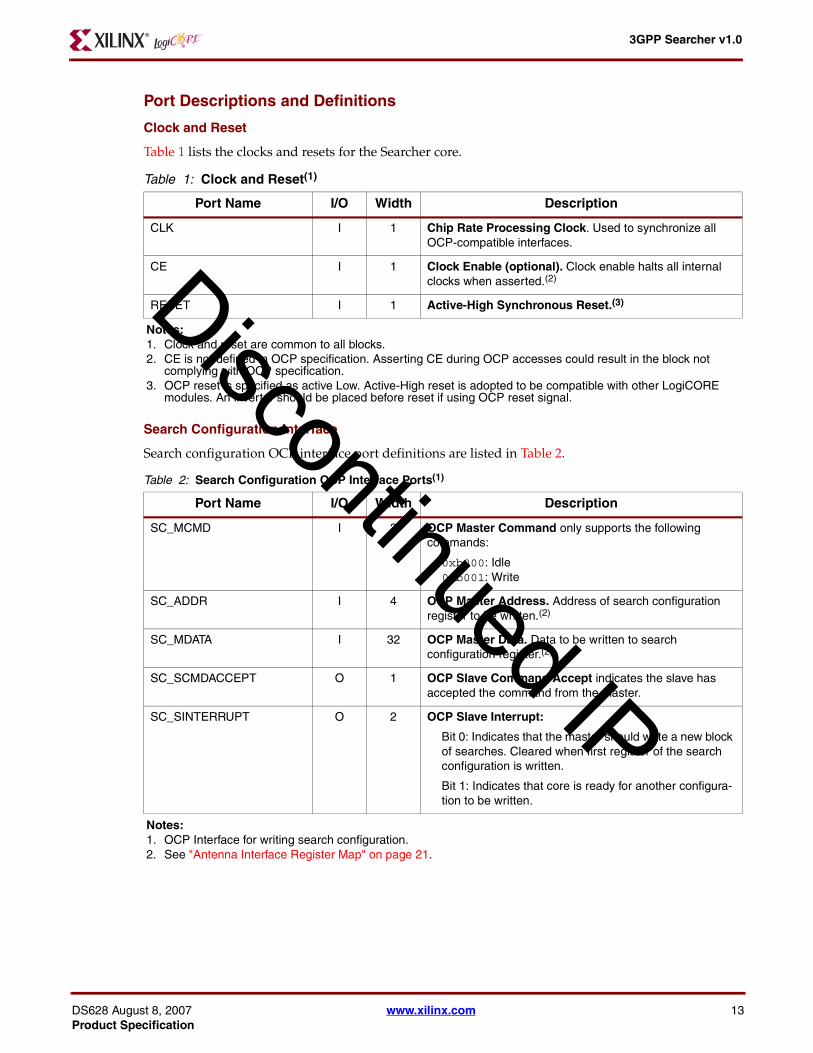
Port Descriptions and Definitions
Clock and Reset
Table 1 lists the clocks and resets for the Searcher core.
Search Configuration Interface
Search configuration OCP interface port definitions are listed in Table 2.
Table 1: Clock and Reset(1)
Port Name I/O Width Description
CLK I 1 Chip Rate Processing Clock. Used to synchronize all OCP-compatible interfaces.
CE I 1 Clock Enable (optional). Clock enable halts all internal clocks when asserted.(2)
RESET I 1 Active-High Synchronous Reset.(3)
Notes: 1. Clock and reset are common to all blocks.2. CE is not defined in OCP specification. Asserting CE during OCP accesses could result in the block not
complying with OCP specification. 3. OCP reset is specified as active Low. Active-High reset is adopted to be compatible with other LogiCORE
modules. An inverter should be placed before reset if using OCP reset signal.
Table 2: Search Configuration OCP Interface Ports(1)
Port Name I/O Width Description
SC_MCMD I 3 OCP Master Command only supports the following commands:
0xb000: Idle 0xb001: Write
SC_ADDR I 4 OCP Master Address. Address of search configuration register to be written.(2)
SC_MDATA I 32 OCP Master Data. Data to be written to search configuration register.(2)
SC_SCMDACCEPT O 1 OCP Slave Command Accept indicates the slave has accepted the command from the master.
SC_SINTERRUPT O 2 OCP Slave Interrupt:
Bit 0: Indicates that the master should write a new block of searches. Cleared when first register of the search configuration is written.
Bit 1: Indicates that core is ready for another configura-tion to be written.
Notes: 1. OCP Interface for writing search configuration.2. See "Antenna Interface Register Map" on page 21.
Discontinued IP
ust 8, 2007 www.xilinx.com 13ecification

3GPP Searcher v1.0
14
Antenna Data Interface
Table 3 describes the antenna data OCP interface ports.
Search Results Interface
Table 4 defines the search results OCP interface ports.
Table 3: Antenna Data OCP Interface Ports(1)
Port Name I/O Width Description
A_MCMD I 1 OCP Master Command. Only supports the following commands:
0xb000: idle 0xb001: write
A_MDATA I 16 Antenna Data. I and Q sample data for the antenna.(2)
A_MDATAINFO I 1 OCP Master Data Info. Bit 0 is set when sample data is synchronized to external timing reference. All offsets in the search configuration are relative to this reference. Only set for data on antenna 0.
A_SCMDACCEPT O 1 OCP Slave Command Accept indicates the slave has accepted the command from the master.
A_SINTERRUPT O 1 OCP Slave Interrupt indicates that the slave is expecting a sample synchronized to external timing reference. Cleared when data is written with A_MDATAINFO[0] set.
Notes: 1. Antenna data is time-interleaved on the interface.2. See "Antenna Interface Register Map" on page 21.
Table 4: Search Results OCP Interface Ports
Port Name I/O Width Description
SR_MCMD I 3 OCP Master Command. Valid Commands are:
0b000 : idle 0b010 : read
SR_MADDR I 23 OCP Master Address. Address specifying PDP and delay offset in PDP to be read.(1)
SR_SDATA O 18 OCP Data. PDP result data.(1)
SR_SDATAINFO O 1 OCP Data Information.
Bit 0: Indicates that saturation has occurred for this PDP. Cleared using the CLEAR_SAT field in search configura-tion register 0.
SR_SRESP O 2 OCP Slave Response. Valid values are:
0b00 : null response 0b01 : data valid response
SR_SCMDACCEPT O 1 OCP Command Accept.
Discontinued IP
www.xilinx.com DS628 August 8, 2007Product Specification

3GPP Searcher v1.0
DS628 AugProduct Sp
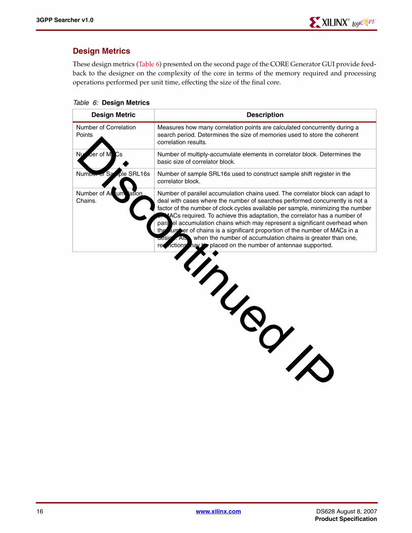
Core Generation and CustomizationThe 3GPP Searcher core is generated and parameterized through the customize option of CORE Gen-erator™ software. The customization GUI also provides feedback about the complexity of the designthrough a number of design metrics displayed on the second page of the GUI.
GUI Parameters
Core parameters that can be set via the CORE Generator GUI are listed in Table 5.
SR_SINTERRUPT O 1 OCP Slave Interrupt indicates completion of a block of search, and that results can be read from the results memory. Cleared by reading memory.
Notes: 1. See "Search Result Memory Map" on page 21.
Table 5: GUI Parameters
Parameter Values Description
Clock Enable True, FalseTrue = component has CE pinFalse = component does not have CE pin
Oversample_Rate 1, 2, 4, 8 Number of samples per chip in antenna data stream(1).
Clock_Rate 8 … 256Number of clock cycles available to process one chip. Clock rate must be a multiple of the oversample rate(2).
Antennae 1 ...16Number of antennae. Must be smaller or equal to number of clocks per sample (clock rate divided by oversample rate).
Quantization 4 … 8 Number of bits used to represent samples.
PDP_Length 4, 8, 16, 32, 64,128, 256Length of PDP generated by a search expressed in chips. Same as the basic window used to accumulate the correlation results.
Number_of_Searches 1 … 256Number of searches that are can be calculated concurrently during a search period.
Number_of_Results 1 … 1024Number of result PDPs stored in the search results memory.
Search_Length 2560 … 38400 Length of search period expressed in chips. Must be a multiple of the PDP Length.(3)
Notes: 1. Oversample_Rate corresponds to O in Figure 6 on page 8.2. Clock_Rate corresponds to the product of parameters O and L in Figure 6 on page 83. This parameter determines the search period as shown in Figure 7 on page 9.
Table 4: Search Results OCP Interface Ports
Port Name I/O Width Description
Discontinued IP
ust 8, 2007 www.xilinx.com 15ecification
3GPP Searcher v1.0
16
Design Metrics
These design metrics (Table 6) presented on the second page of the CORE Generator GUI provide feed-back to the designer on the complexity of the core in terms of the memory required and processingoperations performed per unit time, effecting the size of the final core.
Table 6: Design Metrics
Design Metric Description
Number of Correlation Points
Measures how many correlation points are calculated concurrently during a search period. Determines the size of memories used to store the coherent correlation results.
Number of MACs Number of multiply-accumulate elements in correlator block. Determines the basic size of correlator block.
Number of Sample SRL16s Number of sample SRL16s used to construct sample shift register in the correlator block.
Number of Accumulation Chains.
Number of parallel accumulation chains used. The correlator block can adapt to deal with cases where the number of searches performed concurrently is not a factor of the number of clock cycles available per sample, minimizing the number of MACs required. To achieve this adaptation, the correlator has a number of parallel accumulation chains which may represent a significant overhead when the number of chains is a significant proportion of the number of MACs in a design. Also, when the number of accumulation chains is greater than one, restrictions may be placed on the number of antennae supported.
Discontinued IP
www.xilinx.com DS628 August 8, 2007Product Specification

3GPP Searcher v1.0
DS628 AugProduct Sp
Register and Memory Maps
Searcher Core Operational Flow
The following sections define the register and memory maps for the three OCP-compatible interfaces inthe 3GPP Searcher core. Figure 10 shows the typical operational flow of these registers. The operationof the 3GPP Searcher core is pipelined based on search periods. The length of a search period is deter-mined by the Search_Length parameter of the core.
In the first search period, the block of search configurations is written to the Searcher core via the searchconfiguration registers (“Write Config 0" in Figure 10). The search configuration contains details of thesearch including the result ID of the PDP where the result is stored, or updated. At the start of the nextsearch period, the Searcher core starts searching on the new block of configurations (“Search on Config 0"in Figure 10). The core then correlates against data written on the antenna interface. After the end of thesearch, the PDP results can be read via the search result memory (“Read Results for Config 0" inFigure 10).
Figure Top x-ref 10
Figure 10: Searcher Core Pipelined Operation
Write Config 1 Write Config 2Write Config 0
Read Results for Config 3 Read Results for Config 0Read Results for Config 2
Result ID 12:
Result ID 13:
Result ID 15:
Result ID 0:
Result ID 1:
Result ID 3:
Result ID 8:
Result ID 10:
Result ID 11:
Result ID 9:
Result ID 14: Result ID 2:
Search 0: Result ID 0, 5 Pilots...Search 1: Result ID 1, 6 Pilots...Search 2: Result ID 2, 4 Pilots...Search 3: Result ID 3, 3 Pilots..
Search 0: Result ID 4, 8 Pilots...Search 1: Result ID 5, 3 Pilots...Search 2: Result ID 6, 6 Pilots...Search 3: Result ID 7, 4 Pilots...
Search 0: Result ID 8, 6 Pilots...Search 1: Result ID 9, 6 Pilots...Search 2: Result ID 10, 7 Pilots...Search 3: Result ID 11, 5 Pilots...
ds628_11_061207
Search on Config 0 Search on Config 1Search on Config 3
Discontinued IP
ust 8, 2007 www.xilinx.com 17ecification

3GPP Searcher v1.0
18
Search Configuration Interface
Search Configuration Register Map
Table 7 defines the search configuration register map.
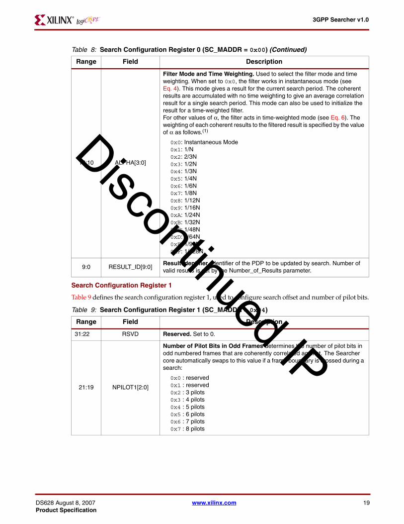
Search Configuration Register 0
Table 8 defines the search configuration register 0, used for configuring PDP results processing.
Table 7: Search Configuration Register Map (SC_MADDR)
Address Description
0x00 Search Configuration Register 0 contains configuration for the results processing.
0x04 Search Configuration Register 1 configures the delay offset and other aspects of search.
0x08 Search Configuration Register 2 configures the scrambling code and the antenna to be searched on.
0x12 Search Configuration Register 3. Writing to this register causes the search configuration to be transferred to the scramble advance unit. Further writes to the search configuration registers are ignored until the scramble advance unit completes advancing the scrambling code.(1)
Note:1. See "Search Results Interface" on page 26 for timing details.
Table 8: Search Configuration Register 0 (SC_MADDR = 0x00)
Range Field Description
31:20 RSVD Reserved. Set to 0.
19 ENABLESearch Enable.
0x0 : Search Disabled.0x1 : Search Enabled.
18 CLEAR_SAT
Clear Saturation Flag
0 : Do not clear Saturation flag.1 : Clear Saturation flag.
This bit is used to clear the saturation flag for the PDP with the specified result index. The saturation flag is reported on the SR_SDATANFO[0] pin. The bit is cleared when the result PDP is updated. Used in conjunction with the PWR_SHIFT field which adjusts the power gain on a particular search.
17:14PWR_SHIFT[3:0] Power Shift. Shifts power results by specified amount. Power is saturated if
power shift overflows.
Discontinued IP
www.xilinx.com DS628 August 8, 2007Product Specification
3GPP Searcher v1.0
DS628 AugProduct Sp
Search Configuration Register 1
Table 9 defines the search configuration register 1, used to configure search offset and number of pilot bits.
13:10 ALPHA[3:0]
Filter Mode and Time Weighting. Used to select the filter mode and time weighting. When set to 0x0, the filter works in instantaneous mode (see Eq. 4). This mode gives a result for the current search period. The coherent results are accumulated with no time weighting to give an average correlation result for a single search period. This mode can also be used to initialize the result for a time-weighted filter.For other values of α, the filter acts in time-weighted mode (see Eq. 6). The weighting of each coherent results to the filtered result is specified by the value of α as follows.(1)
0x0: Instantaneous Mode0x1: 1/N0x2: 2/3N0x3: 1/2N0x4: 1/3N0x5: 1/4N0x6: 1/6N0x7: 1/8N0x8: 1/12N0x9: 1/16N0xA: 1/24N0xB: 1/32N0xC: 1/48N0xD: 1/64N0xE: 1/96N0xF: 1/128N
9:0 RESULT_ID[9:0]Result Identifier. Identifier of the PDP to be updated by search. Number of valid results is set by the Number_of_Results parameter.
Table 9: Search Configuration Register 1 (SC_MADDR = 0x04)
Range Field Description
31:22 RSVD Reserved. Set to 0.
21:19 NPILOT1[2:0]
Number of Pilot Bits in Odd Frames determines the number of pilot bits in odd numbered frames that are coherently correlated against. The Searcher core automatically swaps to this value if a frame boundary is crossed during a search:
0x0 : reserved0x1 : reserved0x2 : 3 pilots0x3 : 4 pilots0x4 : 5 pilots0x5 : 6 pilots0x6 : 7 pilots0x7 : 8 pilots
Table 8: Search Configuration Register 0 (SC_MADDR = 0x00) (Continued)
Range Field Description
Discontinued IP
ust 8, 2007 www.xilinx.com 19ecification

3GPP Searcher v1.0
20
Search Configuration Register 2
Table 10 defines the search configuration register 2. This register configures the scrambling code andantenna.
Search Configuration Register 3
Table 11 defines the search configuration register 3. Writing to this register causes the search configura-tion to be transferred to the scramble advance unit. The register is a dummy register with no contents,and its only effect is to start the scramble advance unit. While the scramble advance unit is operating,further register writes are ignored (see "Search Configuration Interface Timing" on page 22“).
18:16 NPILOT0[2:0]
Number of Pilot Bits in Even Frames. Determines the number of pilot bits in even numbered frames that are coherently correlated against. The Searcher core automatically swaps to this value if a frame boundary is crossed during a search:
0x0 : reserved0x1 : reserved0x2 : 3 pilots0x3 : 4 pilots0x4 : 5 pilots0x5 : 6 pilots0x6 : 7 pilots0x7 : 8 pilots
15:12 DLY_SLOT[3:0] Slot Delay Offset. Valid values: 0 to 14.
11:0 DLY_CHIP[11:0] Chip Delay offset. Valid values: 0 to 2559.
Table 10: Search Configuration Register 2 (SC_MADDR = 0x08)
Range Field Description
31:30 RSVD Reserved. Set to 0.
29:24 ANTENNA[5:0] Antenna to Run Search On. Valid values are 0 to number of antenna minus 1.
23:0 SCR0[23:0] Initial Value of X LFSR Register to generate scramble code.
Table 11: Search Configuration Register 3 (SC_MADDR = 0x12)
Range Field Description
31:0 RSVD Reserved. Set to 0.
Table 9: Search Configuration Register 1 (SC_MADDR = 0x04) (Continued)
Range Field Description
Discontinued IP
www.xilinx.com DS628 August 8, 2007Product Specification

3GPP Searcher v1.0
DS628 AugProduct Sp
Antenna Interface Register Map
Antenna Data
Table 12 defines the antenna data fields.
Search Result Memory Map
The result PDPs are updated when a search is being run, every time the end of a coherent correlationoccurs. For searches using the time-weighted filtering (ALPHA_IDX field not equal to 0), then theresults will be valid through-out a search. For searches using the accumulation mode (no filtering), thenthe results are only valid at the end of a search. In this case, if performing a search on the same user inthe next search period, then the search should be configured to use a different result ID, so that the pre-vious search result can be read safely.
Search Result Memory Map
Search Result Data
Table 12: Antenna Data Fields (A_MDATA[15:0])
Range Field Description
15:8 QDATAQ Component of Sample (2's complement number). Valid range is determined by Quantization core parameter.
7:0 IDATAI Component of Sample (2's complement number). Valid range is determined by Quantization core parameter.
Table 13: Search Results Address: SR_MADDR[22:0](1)
Range Field Width Description
22:13 RESULT 10Result Identifier Identifies PDP. Valid values are:
0 to Number_of_Results – 1.
12:2 DLY 11 Delay Offset of result. Valid values are:
0 to PDP Length × Oversample Rate – 1.
1:0Word
Alignment2 OCP Word Alignment. Bits set to 0.
Note:1. Address space is configured for maximum window size and maximum number of results. Unused bits for
smaller designs should are set to 0.
Table 14: Search Result Data: SR_MDATA[17:0](1)
Range Field Description
17:0 PWR Power
Note:1. Returns power for PDP and offset specified in address.
Discontinued IP
ust 8, 2007 www.xilinx.com 21ecification

3GPP Searcher v1.0
22
Timing DiagramsThe 3GPP Searcher core uses OCP-compatible v2.0 interfaces for each of the main interfaces, allowingthe interfaces to be easily adapted to a variety of bus protocols.
Search Configuration Interface Timing
The search configuration interface is a write-only OCP-compatible interface used to write the searchconfiguration to the 3GPP Searcher core. Figure 11 shows the timing when writing a block of searchconfigurations to the core. The transfer is initiated by the core asserting SC_SINTERRUPT[0], indicat-ing the core is ready for a new block of search configurations to be written. The interrupt is clearedwhen the first configuration word is written.
The search configuration registers are written with configuration data as specified in the register mapgiven in "Antenna Interface Register Map" on page 21. The final register written is search configurationregister 3, causing the search configuration to be transferred to the scramble advance block. While thescramble advance block is advancing the scramble code, further data cannot be written.
The second interrupt flag SC_SINTERRUPT[1] is used to indicate when further data can be written tothe search configuration. This interrupt can also be used as a DMA request signal. When a complete blockof search configuration is written, the DMA request is not re-asserted. The request is only re-assertedwhen the next search period starts, and a further block of search configurations can be written.
Antenna Interface Timing
The antenna interface is a write-only OCP-compatible interface. As shown in Figure 12, antenna data iswritten as a block starting with the lowest numbered antenna, with the transfer repeating every sampleperiod. The signal A_SCMDACCEPT indicates when the antenna data is expected.
The timing diagram in Figure 12 is dependent on a number of the core parameters. The number ofantenna specifies the length of the burst transferred. The sample period is determined by the core'sclock rate divided by the oversample rate. In this example, the number of antennae is 4, the clock rateis 20, and the oversample rate is 2, giving a sample period of 10 clock cycles.
Figure Top x-ref 11
Figure 11: Search Configuration Timing
IDLE WR WR WR IDLE
0x080x040x00
CFG0 CFG1 CFG2
WR WR WR
0x00 0x00 0x08
CFG0 CFG1 CFG2
IDLE
>500 clock cycles
WR IDLE
0x0C0x0C
CFG3 CFG3
WR
CLK
SC_MCMD
SC_MADDR
SC_MDATA
SC_SCMDACCEPT
SC_SINTERRUPT[0]
SC_INTERRUPT[1]
ds628_11_060907
Discontinued IP
www.xilinx.com DS628 August 8, 2007Product Specification

3GPP Searcher v1.0
DS628 AugProduct Sp
The antenna interface is synchronized to the internal processing counts of the core (shown in Figure 6on page 8). The data for antenna 0 is transferred when the cycle count is 0, antenna 1 when cycle countis 1, etc., up to the number of antennae.
The signal A_SCMDACCEPT signal forces the master data transfers to synchronize to the cycle count andthe internally processing rate of the Searcher core (Figure 13). If the master writes data to the core early,then A_SCMDACCEPT is not asserted until the cycle count reaches the correct value, thus throttling themaster data transfer rate.
If the master does not supply antenna data on the expected cycle, then the cycle count is not incre-mented and processing in the core is stalled (Figure 14). Since processing in the core stalls, additionalclock cycles are required to meet the real-time processing requirements of the core.
Figure Top x-ref 12
Figure 12: Antenna Interface Basic Data Transfer
Figure Top x-ref 13
Figure 13: Core Throttling Master Transfer Rate
IDLE WR WR WR WR IDLE
A0 A1 A2 A3 A0 A1 A2 A3
WR WR WR WR IDLE
Sample Period
0 1 2 3 4 5 6 7 8 9 0 1 2 3 4 590
1 0 1
CLK
A_MCMD
A_MDATA
A_SCMDACCEPT
Cycle Count
Oversample Count
ds628_12_060907
IDLE WR WRWRWR IDLE
A0 A1 A2 A3
8 9 0 1 2 3 4 5 6 776
1 0
CLK
A_MCMD
A_MDATA
A_SCMDACCEPT
Cycle Count
Oversample Count
ds628_13_060907
Discontinued IP
ust 8, 2007 www.xilinx.com 23ecification

3GPP Searcher v1.0
24
Figure 15 shows the synchronization of the core to an external framing reference. The signalA_MDATAINFO is asserted when writing the first sample of antenna zero when frame synchronizationoccurs. The signal A_SINTERRUPT indicates that the core is expecting the frame synchronization.A_MDATAINFO, and A_SINTERRUPT occur at the same time when the core is synchronized. The offsetsspecified in the search configuration are used to offset the searches from this reference point.
Figure Top x-ref 14
Figure 14: Master Throttling Core Processing Rate
Figure Top x-ref 15
Figure 15: Antenna Data Frame Synchronization
IDLE WR WRWRWR IDLE
A0 A1 A2 A3
8 9 0 1 2 3 4 5 6 7
1 0
CLK
A_MCMD
A_MDATA
A_SCMDACCEPT
Cycle Count
Oversample Count
ds628_14_060907
IDLE WR WR WR WR IDLE
A0 A1 A2 A3 A0 A1 A2 A3
WR WR WR WR IDLE
0 1 2 3 4 5 6 7 8 9 0 1 2 3 4 590
0 1 0
2559 0
14 0
CLK
A_MCMD
A_MDATA
A_SCMDACCEPT
A_MDATAINFO
A_SINTERRUPT
Cycle Count
Oversample Count
Chip Count
Slot Countds628_15_060907
Discontinued IP
www.xilinx.com DS628 August 8, 2007Product Specification
3GPP Searcher v1.0
DS628 AugProduct Sp
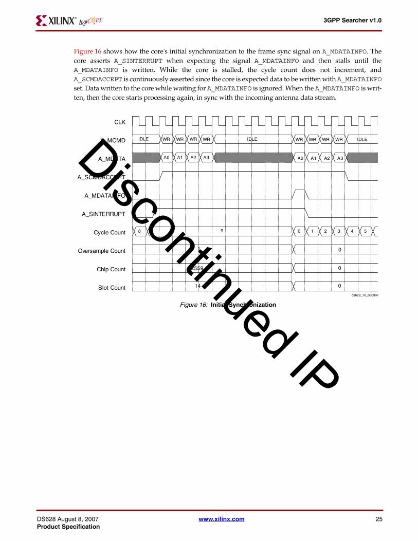
Figure 16 shows how the core's initial synchronization to the frame sync signal on A_MDATAINFO. Thecore asserts A_SINTERRUPT when expecting the signal A_MDATAINFO and then stalls until theA_MDATAINFO is written. While the core is stalled, the cycle count does not increment, andA_SCMDACCEPT is continuously asserted since the core is expected data to be written with A_MDATAINFOset. Data written to the core while waiting for A_MDATAINFO is ignored. When the A_MDATAINFO is writ-ten, then the core starts processing again, in sync with the incoming antenna data stream.
Figure Top x-ref 16
Figure 16: Initial Synchronization
IDLE WR WR WR WR IDLE
A0 A1 A2 A3 A0 A1 A2 A3
WR WR WR WR IDLE
0 1 2 3 4 598
1 0
2559 0
14 0
CLK
A_MCMD
A_MDATA
A_SCMDACCEPT
A_MDATAINFO
A_SINTERRUPT
Cycle Count
Oversample Count
Chip Count
Slot Countds628_16_060907
Discontinued IP
ust 8, 2007 www.xilinx.com 25ecification

3GPP Searcher v1.0
26
Search Results Interface
The search result interface is a pipelined read-only OCP-compatible interface. The signalSR_SINTERRUPT indicates when a current block of searches is complete, and the results can be read(Figure 17). The results can be read. The first read from the memory clears the interrupt.
The results are read for each PDP using the address specified in "Register and Memory Maps" onpage 17. After issuing the OCP read command, there is a three-clock latency from the SR_SCMDACCEPTassertion to data valid as indicated by the signal SR_SRESP.
Figure Top x-ref 17
Figure 17: Search Results Timing
IDLE RD RD RD RD IDLE
A3A2A1A0
D0 D1 D2 D3
VALIDVALIDVALIDVALIDNULL NULLNULL
3 Clock Latency
CLK
SR_SINTERRUPT
SR_MCMD
SR_MADDR
SR_SCMDACCEPT
SR_SRESP
SR_SDATAds628_17_060907
Discontinued IP
www.xilinx.com DS628 August 8, 2007Product Specification
3GPP Searcher v1.0
DS628 AugProduct Sp
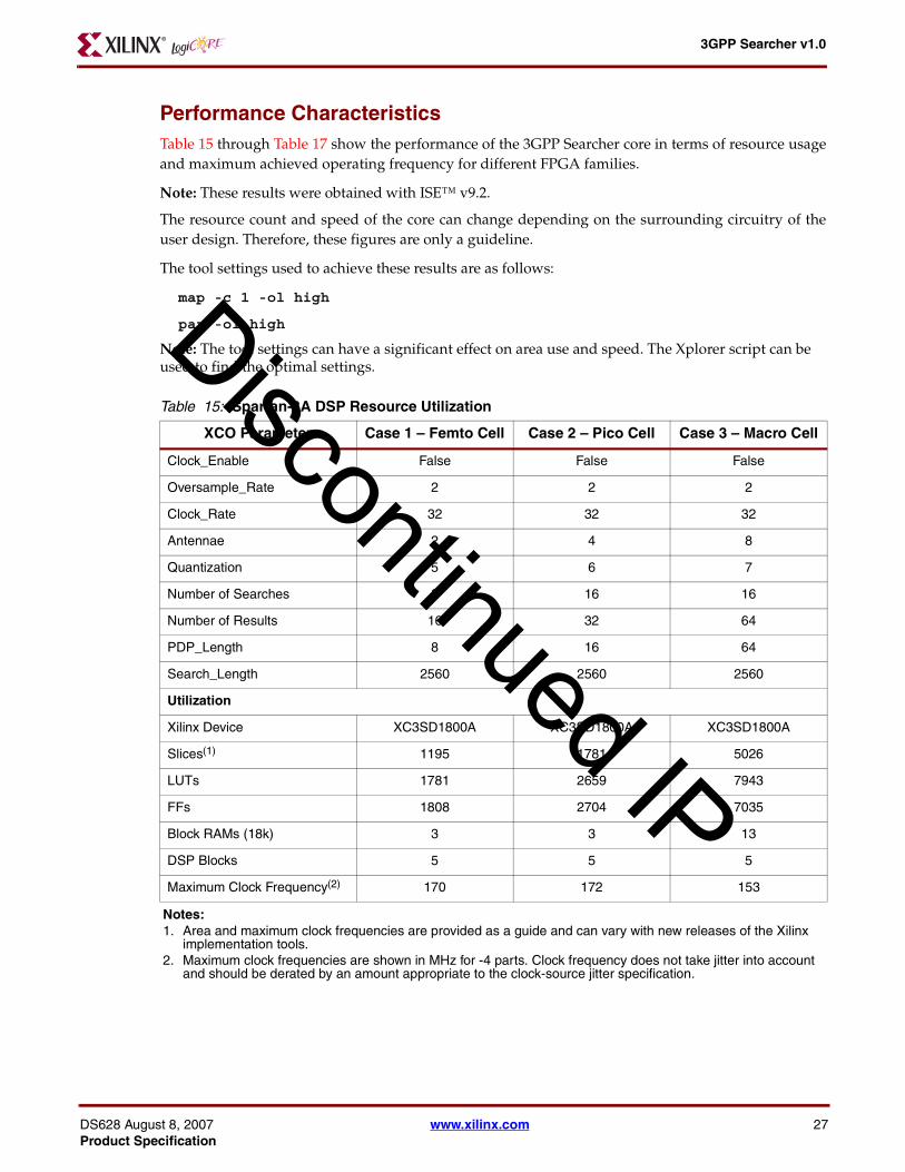
Performance CharacteristicsTable 15 through Table 17 show the performance of the 3GPP Searcher core in terms of resource usageand maximum achieved operating frequency for different FPGA families.
Note: These results were obtained with ISE™ v9.2.
The resource count and speed of the core can change depending on the surrounding circuitry of theuser design. Therefore, these figures are only a guideline.
The tool settings used to achieve these results are as follows:
map -c 1 -ol high
par -ol high
Note: The tool settings can have a significant effect on area use and speed. The Xplorer script can be used to find the optimal settings.
Table 15: Spartan-3A DSP Resource Utilization
XCO Parameter Case 1 – Femto Cell Case 2 – Pico Cell Case 3 – Macro Cell
Clock_Enable False False False
Oversample_Rate 2 2 2
Clock_Rate 32 32 32
Antennae 2 4 8
Quantization 5 6 7
Number of Searches 8 16 16
Number of Results 16 32 64
PDP_Length 8 16 64
Search_Length 2560 2560 2560
Utilization
Xilinx Device XC3SD1800A XC3SD1800A XC3SD1800A
Slices(1) 1195 1781 5026
LUTs 1781 2659 7943
FFs 1808 2704 7035
Block RAMs (18k) 3 3 13
DSP Blocks 5 5 5
Maximum Clock Frequency(2) 170 172 153
Notes: 1. Area and maximum clock frequencies are provided as a guide and can vary with new releases of the Xilinx
implementation tools. 2. Maximum clock frequencies are shown in MHz for -4 parts. Clock frequency does not take jitter into account
and should be derated by an amount appropriate to the clock-source jitter specification.
Discontinued IP
ust 8, 2007 www.xilinx.com 27ecification

3GPP Searcher v1.0
28
Table 16: Virtex-4 Resource Utilization
XCO Parameter Case 1 – Femto Cell Case 2 – Pico Cell Case 3 – Macro Cell
Clock_Enable False False False
Oversample_Rate 2 2 2
Clock_Rate64 64 64 64
Antennae 2 4 8
Quantization 5 6 7
Number of Searches 8 16 32
Number of Results 16 32 64
PDP_Length 8 16 32
Search_Length 2560 2560 2560
Utilization
Xilinx Device XC4VLX25 XC4VLX25 XC4VLX25
Slices(1) 1028 1348 2769
LUTs 1696 2283 5195
FFs 1691 2200 4245
Block RAMs (18k) 3 3 10
DSP Blocks 5 5 5
Maximum Clock Frequency(2) 270/339 263/329 249/301
Notes: 1. Area and maximum clock frequencies are provided as a guide. They may vary with new releases of the Xilinx
implementation tools. 2. Maximum clock frequencies are shown in MHz for -10/-12 parts. Clock frequency does not take jitter into
account and should be derated by an amount appropriate to the clock-source jitter specification.
Discontinued IP
www.xilinx.com DS628 August 8, 2007Product Specification

3GPP Searcher v1.0
DS628 AugProduct Sp
Support Xilinx provides technical support for this LogiCORE product when used as described in the productdocumentation. Xilinx cannot guarantee timing, functionality, or support of product if implemented indevices that are not defined in the documentation, if customized beyond that allowed in the productdocumentation, or if changes are made to any section of the design labeled DO NOT MODIFY.
Table 17: Virtex-5 Resource Utilization
XCO Parameter Case 1 – Femto Cell Case 2 – Pico Cell Case 3 – Macro Cell
Clock Enable False False False
Oversample_Rate 2 2 2
Clock_Rate 64 64 64
Antennae 2 4 8
Quantization 5 6 7
Number of Searches 8 16 32
Number of Results 16 32 64
PDP_Length 8 16 32
Search_Length 2560 2560 2560
Utilization
Xilinx Device XC5VLX30 XC5VLX30 XC5VLX30
LUT/FF Pairs(1) 1814 2348 4414
LUTs 926 1262 2834
FFs 1688 2197 4180
Total Block RAMs(3)
Block RAMs (36k) 0 0 2
Block RAMs (18k) 3 3 6
DSP Blocks 5 5 5
Maximum Clock Frequency(1,2) 287/378 276/364 260/332
Notes: 1. Area and maximum clock frequencies are provided as a guide. They may vary with new releases of the Xilinx
implementation tools. 2. Maximum clock frequencies are shown in MHz for -1/-3 parts. Clock frequency does not take jitter into account
and should be derated by an amount appropriate to the clock-source jitter specification. 3. Represents the total number of 36k block RAMs used when map is run. In reality, two 18k block RAM primitives
can usually be packed together, giving an absolute minimum total block RAM usage of block RAMs (36k) + (block RAMs (18k) /2) (rounded up).
Discontinued IP
ust 8, 2007 www.xilinx.com 29ecification
3GPP Searcher v1.0
30
Ordering InformationThe 3GPP Searcher core is provided under the SignOnce IP Site License and can be generated using theXilinx CORE Generator software v9.2i or higher. The CORE Generator software is shipped with XilinxISE™ Foundation™ Series Development software.Once purchased, the core may be downloaded from the Xilinx IP Center for use with the Xilinx COREGenerator v9.2i and higher. The Xilinx CORE Generator software is bundled with the ISE Foundationsoftware at no additional charge.
Contact your local Xilinx sales representative for pricing and availability of additional Xilinx Logi-CORE modules and software. Information about additional Xilinx LogiCORE modules is available onthe Xilinx IP Center.
Revision History
Date Version Revision
08/08/07 1.1 Initial Xilinx release
Discontinued IP
www.xilinx.com DS628 August 8, 2007Product Specification