Embed Size (px)
Citation preview
PROPRIETARY RIGHTS STATEMENT
This document contains information, which is proprietary to the Flex5Gware Consortium.
Research and Innovation Action
Flex5Gware Flexible and efficient hardware/software platforms for
5G network elements and devices
H2020 Grant Agreement Number: 671563
WP 4 – 5G Digital front-ends and HW/SW function split
D 4.1 – Requirements and concepts for the digital HW in 5G transceivers
Contractual Delivery Date: 31/12/2015
Actual Delivery Date: 22/12/2015
Responsible Beneficiary: CTTC
Contributing Beneficiaries: CTTC, VTT, CEA, SEQ, IMC, CNIT, TST, UC3M, IMDEA WINGS
Dissemination Level: Public
Version: 1.0

PROPRIETARY RIGHTS STATEMENT
This document contains information, which is proprietary to the Flex5Gware Consortium.
This page is left blank intentionally
H2020 Grant Agreement Number: 671563 Document ID: WP 4 / D 4.1
Dissemination Level:Public Page 3
Document Information
Document ID: D 4.1
Version Date: 22/12/2015
Total Number of Pages: 80
Abstract: This deliverable specifies the design of a number of selected
concepts and solutions of the digital hardware architecture and
the hardware/software function partitioning envisioned in
Flex5Gware. In more detail, the document starts by defining the
requirements of WP4 based on use cases and key performance
indicators defined in WP1. Three major categories of WP4
requirements (with its related sub-requirements) were identified
in this respect covering the planned developments. The
document also presents and specifies the concepts that will be
developed in WP4. Two major categories were defined, with
each one including groupings of different fifth generation
baseband processing concepts. The first covers digital
hardware architectures optimising spectrum and energy
efficiency and the second one digital hardware architectures
optimising flexibility. The mentioned categories are directly
mapped to the tasks T4.2 and T4.3 of the Flex5Gware DoW.
These key concepts do not exhaustively cover the entire fifth
generation digital baseband spectrum but aim at providing
focused innovations at the digital hardware of fifth generation
transceivers.
Keywords: Specifications, requirements, concepts, architecture, design
challenges
Authors
Full Name Beneficiary / Organisation
e-mail Role
Nikolaos Bartzoudis CTTC [email protected] Overall Editor
Oriol Font CTTC [email protected] @cttc.es Contributor
Marco Miozzo CTTC [email protected] Contributor
Paolo Dini CTTC [email protected] Contributor
Vincent Berg CEA [email protected] Contributor
Tushar Gupta CEA [email protected] Contributor
Valentin Savin CEA [email protected] Contributor
Tapio Rautio VTT [email protected] Contributor
Martti Forsell VTT [email protected] Contributor
Guillaume Vivier SEQ [email protected] Contributor
Leonardo Gomes Baltar IMC [email protected] Contributor
H2020 Grant Agreement Number: 671563 Document ID: WP 4 / D 4.1
Dissemination Level:Public Page 4
Kilian Roth IMC [email protected] Contributor
Javier Valiño TST [email protected] Contributor
Panagiotis Vlacheas WINGS [email protected] Contributor
Dimitris Kelaidonis WINGS [email protected] Contributor
Evaggelia Tzifa WINGS [email protected] Contributor
Aikaterini Demesticha WINGS [email protected] Contributor
Vera Stavroulaki WINGS [email protected] Contributor
Orestis Liakopoulos WINGS [email protected]
Contributor
Ilenia Tinnirello CNIT [email protected] Contributor
Pablo Serrano Yañez-Mingot
UC3M [email protected] Contributor
Iñaki Ucar UC3M [email protected] Contributor
Carlos Donato IMDEA [email protected] Contributor
Domenico Giustiniano IMDEA [email protected] Contributor
Reviewers
Full Name Beneficiary / Organisation
e-mail Date (review delivery date after 2nd review)
Michael Färber IMC [email protected] 15/12/2015
Frederik Tillman EAB [email protected] 15/12/2015
Dieter Ferling ALUD [email protected]
15/12/2015
Version history
Version Date Comments
1.0 22/12/2015 Final version of the document.
H2020 Grant Agreement Number: 671563 Document ID: WP 4 / D 4.1
Dissemination Level:Public Page 5
Executive Summary
This document aims at defining the requirements, specifications and derived concepts of the 5G digital hardware architectures. These, among others, include mechanisms, schemes and algorithms that foster a flexible hardware/software baseband function partitioning, as a means to provide significant operating benefits. Towards this end, the document analyses first the use cases, key performance indicators and requirements defined in WP1, in order to identify those that are especially relevant to the tasks to be carried out in WP4. Their relation with the other work packages of Flex5Gware project is also contemplated. Section 2 also defines three major categories of requirements specific for 5G digital front ends; each of these three categories was populated with an extensive list of sub-requirements. The core of this deliverable presents the specifications and design objectives of a number of digital hardware concepts and solutions that aim at serving focused 5G use cases and satisfy specific WP4 requirements. The goal of these WP4 digital hardware concepts is to provide 5G wireless systems able to improve capacity, reduce power consumption and increase flexibility. Although the defined concepts and solutions do not cover the entire 5G digital HW operating needs, they constitute a representative part of the digital hardware panorama in the forthcoming generation of mobile communication systems. In broad terms, the WP4 concepts and solutions are related to:
Digital hardware architectures of new 5G waveforms and transceiver optimizations to satisfy performance/complexity trade-offs.
Efficient multiple input multiple output and forward error correction decoders whose goal is to increase data throughput and reduce the power consumption of digital circuits.
Flexible hardware/software architectures that enhance reconfigurability, scalability, modularity and cover the inclusion of external sensing devices in context-aware communications.
Dynamic partitioning and reprogramming of communication stacks functions to different processing elements across the 5G network.
H2020 Grant Agreement Number: 671563 Document ID: WP 4 / D 4.1
Dissemination Level:Public Page 6
Table of Contents
1. Introduction .................................................................................................. 11
1.1 Objectives ............................................................................................................12 1.2 Relation with other WPs .....................................................................................12 1.3 Organization of the document ...........................................................................12
2. Requirements of 5G digital baseband processing .................................... 13
2.1 Scenarios, use cases and KPIs ..........................................................................13 2.2 Digital HW requirements related to use cases and KPIs ..................................17 2.2.1 Digital HW architecture (ARCH) ........................................................................20 2.2.2 Digital HW components (COMP) .......................................................................21 2.2.3 HW/SW implementation (IMPL) ........................................................................22
3. Specifications of key concepts in 5G digital baseband processing ....... 23
3.1 Introduction .........................................................................................................23 3.1.1 Synergies and collaborations ............................................................................24 3.2 Digital HW architectures optimising spectrum and energy efficiency ............26 3.2.1 5G waveforms and multi-antenna schemes ......................................................26
3.2.1.1 Implementation of new Waveforms and MIMO Equalization Techniques ...26 3.2.1.2 FBMC structures for 5G .............................................................................29
3.2.2 Coding solutions for 5G .....................................................................................37 3.2.2.1 Efficient high performance LDPC decoding ...............................................37 3.2.2.2 Turbo decoder design optimized for Massive IoT ......................................41
3.2.3 Multiprocessor baseband architectures for 5G network elements .....................44 3.3 Digital HW architectures optimising flexibility ..................................................47 3.3.1 Flexible HW-SW partitioning solutions for 5G ....................................................47
3.3.1.1 Architecture for supporting MAC/PHY cross-layer reconfigurations ...........47 3.3.1.2 Flexible partitioning of SW & HW communication stack functions ..............54 3.3.1.3 Cognitive dynamic HW/SW partitioning algorithm ......................................63
3.3.2 Context-aware 5G solutions ..............................................................................67 3.3.2.1 Sensor data use on 5G cells ......................................................................67 3.3.2.2 Energy profiling information for flexible 5G networking ..............................71 3.3.2.3 Ranging algorithms for anticipatory networks ............................................73
4. Conclusions ................................................................................................. 76
5. References ................................................................................................... 77

H2020 Grant Agreement Number: 671563 Document ID: WP 4 / D 4.1
Dissemination Level: Public Page 7
List of abbreviations
1G – First generation of mobile cellular network
2G – Second generation of mobile cellular network
3G – Third generation of mobile cellular network
3GPP – 3rd Generation Partnership Project
4G – Fourth generation of mobile cellular network
5G – Fifth generation of mobile cellular network
ACK – Acknowledgement
ADC – Analogue-to-Digital Converter
ALU – Arithmetic Logical Unit
AP – Access Point
API – Application Programming Interface
ARCH – Digital Hardware Architecture (WP4 Requirement)
ASIC – Application-Specific Integrated Circuit
AXI – Advanced eXtensible Interface
BCJR – Bahl-Cocke-Jelinek-Raviv
BRAM – Block Random access memory
CB – Code Block
CFO – Carrier Frequency Offset
CMOS – complementary metal-oxide semiconductor
CMP – Chip Multiprocessor
CNU – Check-Node Unit
COMP – Digital Hardware Components (WP4 Requirement)
CP – Cyclic Prefix
CPRI – Common Public Radio Interface
CSMA – Carrier Sense Multiple Access
DAC – Digital-to-Analogue Converter
DAQ – Data Acquisition
DCF – Distributed Coordination Function
DL – DownLink
DoW – Description of Work
DRP – Dynamic Reconfiguration Port
DSP – Digital Signal Processing
DUT – Device Under Test
DVB – Digital Video Broadcasting
EPC - Evolved Packet Core
FBMC – Filterbank Multicarrier (modulation)
H2020 Grant Agreement Number: 671563 Document ID: WP 4 / D 4.1
Dissemination Level: Public Page 8
FD – Frequency Domain
FDD – Frequency-Division Duplex
FDMA – Frequency Division Multiple Access
FEC – Forward Error Correction
FFT – Fast Fourier Transform
FPGA – Field Programmable Gate Array
FS – Frequency Spreading
GA - Genetic Algorithm
GFDM – Generalized Frequency Division Multiplexing
GigE – Gigabit Ethernet
GPC – General Purpose Computer
GPP – General Purpose Processor
HW – Hardware
HWA – Hardware-Accelerated
ILP – Instruction-Level Parallelism
IMPL –Hardware/Software Implementation (WP4 Requirement)
IN – Intermediate Node
IoT – Internet of Things
IP – Intellectual Property
KPI - Key Performance Indicator
LDPC – Low Density Parity Check
LLR – Log-Likelihood Ratio
LMU – Local Memory Unit
LTE – Long Term Evolution
LTE-A – Long Term Evolution Advanced
MAC – Medium Access Protocol
MAP – Maximum A Posteriori
MBSFN – Multicast-broadcast single-frequency network
MBTAC – MultiBunched/Threaded Architecture Chaining
MC – Multi Carrier
MCS – Modulation Coding Scheme
MIMD – Multiple Instruction Stream Multiple Data Stream
MIMO – Multiple Input Multiple Output
MMCM – Mixed-Mode Clock Manager
mmWave – Millimetre Wave
MOPSO-CD - Multi-objective Particle Swarm Optimization with Crowding Distance
MP – Message-Passing
H2020 Grant Agreement Number: 671563 Document ID: WP 4 / D 4.1
Dissemination Level: Public Page 9
MS – Min-Sum
MTC – Machine Type Communications
MU – Memory Unit
NFV – Network Function Virtualization
NMS – Normalized Min-Sum
NoC – Network-on-Chip
NSGA - Non Dominated Sorting Genetic
NUMA – Non-Uniform Memory Access
OFDM – Orthogonal Frequency Division Multiplexing
OMS – Offset Min-Sum
P-RNTI – Paging Radio Network Temporary Identifier
PBCH – Physical Broadcast Channel
PCCC – Parallel Concatenated Convolutional Coding
PCFICH – Physical Control Format Indicator Channel
PDCCH – Physical Downlink Control Channel
PDCP – Packet Data Convergence Protocol
PDSCH – Physical Downlink Shared Channel
PHY - Physical layer
PoC – Proof-of-Concept
PPN – PolyPhase Network
PRAM – Parallel Random Access Machine
PS-RNTI – Semi-persistent Scheduling Information Radio Network Temporary Identifier
PU – Processing Unit
QAM – Quadrature Amplitude Modulation
QPP – Quadrature permuted polynomial
RA-RNTI – Random Access Radio Network Temporary Identifier
RLC – Radio Link Control
RNTI – Radio Network Temporary Identifier
RRM – Radio Resource Management
RSC – Recursive Systematic Convolutional
RTOS – Real-Time Operating System
SDN – Software Defined Networking
SDR – Software Defined Radio
SHM – Shared Memory
SI-RNTI – System Information Radio Network Temporary Identifier
SIFS – Short Inter-Frame Space
SISO – Single Input Single Output
H2020 Grant Agreement Number: 671563 Document ID: WP 4 / D 4.1
Dissemination Level: Public Page 10
SoC – System-on-Chip
SW – Software
TB – Transport Block
TC-RNTI – Temporary Cell Radio Network Temporary Identifier
TD – Time Domain
TDMA – Time Division Multiple Access
ToF – Time-of-Flight
TTI – Transmission Time Interval
UC – Use Case
UE – User Equipment
UL – UpLink
UFMC – Universal Filtered Multicarrier (modulation)
UMTS – Universal Mobile Telecommunications System
VLIW – Very Long Instruction Word
VLSI – Very Large Scale Integration
VNU – Variable-Node Unit
Wi-Fi – any "wireless local area network" (WLAN) product
WiMAX – Worldwide Interoperability for Microwave Access
WMP – Wireless MAC Processor
WP – Work Package
WPAN – Wireless Personal Area Network
WSGA - Weighted Sum Genetic Algorithm
XFSM – eXtended Finite State Machine

H2020 Grant Agreement Number: 671563 Document ID: WP 4 / D 4.1
Dissemination Level: Public Page 11
1. Introduction
Flex5Gware aims at providing highly reconfigurable and agile hardware (HW) platforms together with HW-agnostic software (SW) platforms for network elements and user equipment devices able to satisfy increased capacity, reduced energy cost, versatility, scalability and modularity objectives of fifth generation (5G) transceivers. In this context, the purpose of WP4 is to develop spectral efficient, energy efficient and flexible digital front-end concepts and solutions including optimal mechanisms for a seamless partitioning of HW and SW functions. In the present deliverable D4.1, the goal is to define the requirements, specifications and derived concepts of the digital HW architecture and the HW/SW function partitioning. For this purpose, the use cases (UCs) and requirements defined for the project in the deliverable D1.11 are analysed to deduce the requirements transferred to the WP4 digital HW and to the HW/SW function partitioning. In order to tackle the WP4 requirements this deliverable specifies the design of a number of selected concepts and solutions. The requirements focusing on the HW/SW function partitioning, form the connecting link with WP5 “5G SW modules and functions”.
For disambiguation purposes we would like to define and delimit the meaning of “5G Digital front-ends and HW/SW function split”. As it is seen in Figure 1.1, the digital HW communicates from the one end with 5G mixed-signal technologies and from the other end with higher-layer SW modules and functions. Although the digital signal processing (DSP) building blocks share a similar ecosystem with current 4G systems, a key differentiator of Flex5Gware WP4 is that on top of focused DSP solutions that address 5G baseband challenges, it aims at delivering new transversal characteristics such as operational flexibility, programmability and reconfigurability, especially in relation to the partitioning of HW and SW functions.
Figure 1.1: A high-level representation of the WP4 structure and its interactions with WP3 and WP5.
1 Flex5Gware D1.1, “5G Architecture requirements, specifications, and use cases”.

H2020 Grant Agreement Number: 671563 Document ID: WP 4 / D 4.1
Dissemination Level: Public Page 12
1.1 Objectives
The goal of WP4 is to provide digital HW architectures and implementations for 5G wireless systems that will help to improve the achievable capacity, reduce power consumption and increase flexibility. In concrete the following objectives have been defined:
Study the impact on digital HW architectures of new 5G waveforms and explore possible transceiver optimizations for an optimal performance/complexity trade off and understand silicon costs related to the implementation of these new waveforms on digital HW.
Design of flexible and efficient multiple input multiple output (MIMO) and forward error correction (FEC) decoders (including low-density parity-check (LDPC) decoders) geared to increase data throughput and reduce power consumption of digital circuits.
Design a flexible architecture based on HW/SW function partitioning to enhance reconfigurability, scalability and modularity and cover, in an agnostic way, the inclusion of external sensing devices in terminal devices and network elements to address context aware-based communication functionalities.
Investigate the possibility of dynamically shifting and reprogramming functions of communication stacks (mainly from layer 1 to layer 3) to different processing elements available in the network.
1.2 Relation with other WPs
The UCs and key performance indicators (KPIs) defined in WP1 propagate different requirements to the concepts that will be developed in the technical WPs of Flex5Gware and thus to WP4 as well. WP4 is linked with WP3 and WP5 where the optimum division between analogue signal processing, digital HW and SW in 5G transceivers will be explored. The outcome of WP4 also serves as input to WP6 “Proof of concept in Flex5Gware”. As far as the WP1 is concerned, this deliverable considers the work in T1.1 “Use cases and scenarios for 5G systems” and T1.2 “5G system requirements break-down”, ensuring the compliance with D1.1. Furthermore, the concepts and technologies developed in T4.2 “Digital HW architectures optimizing spectrum and energy efficiency” and T4.3 “Digital HW architectures optimizing flexibility”, will provide valuable input to software architecture and modules of WP5. Various developed concepts will be integrated and mapped to demonstration activities of WP6. Finally, results and research findings will be disseminated and exploited according to the plan described in WP7 “Dissemination, Standardization, and Exploitation”.
1.3 Organization of the document
The remaining of the document includes the following sections: Section 2.1 makes a qualitative mapping of WP1 with high level WP4 objectives. Section 2.2 identifies three major requirement categories that WP1 UCs and KPIs transfer to WP4 and creates a list of sub-requirements for each category (i.e., in Subsections 2.2.1, 2.2.2 and 2.2.3). Section 3 is divided in two main Subsections (3.2 and 3.3), which correspond to the T4.2 and T4.3 defined in the Flex5Gware description of work (DoW). Moreover, Section 3.2 and 3.3 are divided in three and two Subsections respectively that group complementary WP4 concepts (including motivation, requirements, and development steps). Finally, Section 4 makes a brief summary of the deliverable conclusions.

H2020 Grant Agreement Number: 671563 Document ID: WP 4 / D 4.1
Dissemination Level: Public Page 13
2. Requirements of 5G digital baseband processing
2.1 Scenarios, use cases and KPIs
Starting from the global objective of Flex5Gware, which is to deliver highly reconfigurable HW together with HW agnostic SW platforms, WP1 has depicted a set of UC families and the associated KPIs in order to drive the work of the technical WPs. To this respect, the objective of this deliverable is to investigate how the UCs and KPIs will affect the specification and design of 5G digital baseband processing.
The three WP1 UC families detailed hereafter, were defined according to the NGNM report [Ngm15], which identifies six relevant UCs. The broadband access in dense areas family aims at providing high data rates in urban and crowded places with a multitude of users demanding high quality of peak rate services. It includes both business needs leisure activities, where a huge number of people are located in potentially small areas and need large data stream services with high reliability. Crowded venues is a representative UC of this family, where many users are temporary located in a small area (e.g., in concerts, public or sports events, etc.) and want to share multimedia content. This implies that uplink (UL) traffic can be higher with respect to downlink (DL) traffic. Another important UC of this family is the dynamic hotspot one, in which momentaneous data offloading of large groups of people have to be handled for occasional periods of time in dense urban scenarios. Similarly to the previous family, broadband access everywhere aims at describing a scenario where high data rates are needed, however in this case with a wider scope, including challenging situations where coverage is a problem or when mobility might create undesired data stream interruptions. This for instance is depicted in the 50+ Mbps everywhere UC, where users need very high data rate in areas with sparse network infrastructure (e.g., cell borders, rural areas). The latter also applies to the connected vehicles UC, where “human-triggered” traffic with mobiles devices have to be managed under challenging signal propagation conditions. This UC also includes “machine initiated” traffic, which introduces a different set of requirements, due its nature (e.g., IoT devices vs. V2X communications). The massive internet of things (IoT) UC family envisages new key features of 5G networks where the number of connections will be demanding and the type of services will have a wide range of characteristics linked to diverse IoT products. An important UC of this family is the Smart cities one, where the network will have to manage the predicted IoT traffic and use the information provided to apply intelligent decisions. The Performance equipment UC targets high end products in terms of data rate, processing power, and user interface. Finally, this UC family also includes the connected vehicles UC which is meant to handle “machine initiated” traffic.
The table that follows lists the defined KPIs in WP1 and highlights how they are related with WP4.
Table 2.1: List of Flex5Gware consolidated KPIs
KPI Acronym Relation with WP4
Flexibility / versatility / re-configurability
FVR
This KPI is of strong interest from the digital HW front-end perspective. The activities in WP4 include both HW components reconfiguration aspects, such as versatile multi-band transceiver implementations, and more system-wide topics, such as flexible HW and SW partitioning of communication stack functions.
Cost CST In WP4 the cost is related a) with the computational cost of the digital front-end (e.g., number of gates, number of processors), which in turn define the cost of components
H2020 Grant Agreement Number: 671563 Document ID: WP 4 / D 4.1
Dissemination Level: Public Page 14
and devices, b) the cost of operation which could be reduced through the flexible HW/SW partitioning and c) the revenues that can be achieved by virtualizing network elements (e.g., virtualize digital front-ends in order to lease them to different operators).
Energy efficiency NRG
In WP4 the energy efficiency can be addressed either a) during the design and implementation time of the digital front-end and b) at run-time through the flexible partitioning of communication stack HW and SW functions. For instance, WP4 will provide application programming interfaces (APIs) to SW for enabling a smart virtualization/reconfiguration according to the energy assessment evaluation performed.
Resilience and continuity
RES
In WP4 the digital HW front-end would have the ability to offer resilience and continuity by a) designing optimal RAT usage according to specific conditions and b) designing reconfiguration mechanisms that secure continuity of the offered service.
Mobile data volume
• Aggregated data rate
• Coverage / ubiquitous access
MDV
This KPI covers both the uplink/downlink cell capacity and the cell edge performance (expressed in terms of guaranteed minimum data rates). In WP4 the activities will concentrate on developing digital HW front-ends that enable the operation in additional frequency bands, including millimetre wave (mmWave), which remarkably increase the operation bandwidth both at system and user level. Moreover, in order to address this KPI in WP4, it is also contemplated the improvement of existing wireless technologies to increase the data volume per geographical area by improving the typical user data rate and by enhancing the number of devices that can be connected at any given time.
Number of users / connected devices
NoU
This KPI is strongly related to WP4 activities; HW enhancements, field programmable HW-accelerated functions and novel digital HW architectures will be explored to satisfy this KPI. At a different level, small cell traffic offloading and optimization of the radio resource management and the medium access control protocol so that users can access the medium more efficiently (e.g., thanks to the dynamic re-configuration of the Medium Access Control (MAC) and upper layers and a more close interaction with physical (PHY) layer) will be contemplated.
Bandwidth
• Radio bandwidth
• Operation bandwidth
BW
This KPI is related to the bandwidth supported by both network nodes and user equipment (UE)/sensors/actuators, which are parameters that have a high impact in digital HW front-end. WP4 activities will tackle these aspects with digital architectures that will be able to support the 5G bandwidth KPIs.

H2020 Grant Agreement Number: 671563 Document ID: WP 4 / D 4.1
Dissemination Level: Public Page 15
Latency LAT
This KPI aims at evaluating the network latency (i.e., end2end round trip time) and also the link latency, for considering HW constraints. The work in WP4 will provide solutions for 5G communication platforms so that the latency can be reduced via the development of efficient digital HW architectures The latency KPI would also be addressed through reconfiguration mechanisms that will flexibly partition the HW/SW functions of the communication stack.
User data rate UDR
This KPI is aimed at ranking the archived end2end data rate, therefore it includes both UL and DL, and moreover it affects both machine type communications (MTC) devices (for IoT) and handheld ones (for human triggered traffic). Indicative WP4 activities related to this KPI are: increasing the user data rate per spectrum unit (e.g., via full duplex operation, the HW support for 5G waveforms like filter bank multi carrier (FBMC), and faster FEC decoding architectures), ii) reducing the experienced interference (e.g., through dynamic base station coordination and/or massive MIMO equalization techniques).
Integration / size / footprint
ISF
This KPI deals with the HW footprint related to its size/volume. WP4 will address this KPI investigating on efficient digital HW front-end architectures and building blocks optimized for UCs (e.g., turbo decoder for IoT, high performance LDPC decoder).
The UCs and the correspondent KPIs represent the guideline for all the Flex5Gware activities toward the development of the proof-of-concepts (PoCs). On this matter, Figure 2 provides a graphic representation of the relation between PoC and UCs. According to this, WP4 has shaped the HW requirements and solutions as it is detailed in the following Subsections.
a) Broadband access in dense areas.
H2020 Grant Agreement Number: 671563 Document ID: WP 4 / D 4.1
Dissemination Level: Public Page 16
b) Broadband access everywhere.
c) Massive Internet of Things.
Figure 2.1: UC families, UCs, and PoC mapping.
H2020 Grant Agreement Number: 671563 Document ID: WP 4 / D 4.1
Dissemination Level: Public Page 17
2.2 Digital HW requirements related to use cases and KPIs
Each UC defined in WP1 is related to a number of KPIs that affects at different levels the digital hardware requirements of 5G transceivers. Hence, in this Section we have identified three major requirement categories that WP1 UCs and KPIs transfer to WP4. The deducted WP4 requirement categories were populated with a respective list of sub-requirements, featuring an identification number, as it is shown later on in Subsections 2.2.1, 2.2.2 and 2.2.3. The specifications of the different concepts and technologies presented in Section 3 satisfy a selection of different WP4 requirements, which relate to the UCs that each Section 3 concept targets. The three identified WP4 requirement categories are the following:
Digital HW architecture (ARCH) o Functional requirements related to the operation of the compound of
processors, memories and communication interfaces comprising the digital hardware architecture. The digital HW architecture can include functionalities in a single device (System-on-Chip –SoC-), in a centralized large processing node, or in a number of distributed processing nodes, including as well virtualized HW sub-architectures. The ARCH requirements assume in all cases a heterogeneous interaction among processors, memories and communication interfaces.
Digital HW components (COMP) o This category includes requirements related to the individual processing,
memory and interconnection elements. Hence the focus of the requirements is narrower in this case. The goal is to delimit and dimension the specific needs of digital HW components in relation to the defined use cases and KPIs.
HW/SW implementation (IMPL) o This category includes requirements related to the implementation of the
HW/SW portions/subsystems comprising the digital HW. The implementation requirements might encompass one or more components and include digital HW and software functions. The requirements at implementation level have as a goal to optimally exploit the underlying resources in order to satisfy higher level KPIs.
Figure 2.2: The relation between use cases KPIs and WP4 requirement categories.
Use cases & KPIs
WP4 requirements
ARCH
IMPL #1
IMPL #2
IMPL #N
···
COMP #1
COMP #2
COMP #3
COMP #4
COMP #5
COMP #N-2
COMP #N-1
COMP #N
···

H2020 Grant Agreement Number: 671563 Document ID: WP 4 / D 4.1
Dissemination Level: Public Page 18
An indicative representation of the requirements that UCs and KPIs pose to WP4 is also shown in Figure 2.2. A detailed mapping of the UCs and their respective KPIs with the requirement categories of WP4 is shown in Table 2.2. A coarse grain scale was adopted (i.e., low, medium, high) to show how each UC and KPI in Flex5Gware affects or relates the ARCH, COMP and IMPL requirements.
Table 2.2: Relationship of WP1 UCs and essential KPIs with WP4 high-level requirements.
Use cases KPIs Relation to WP4
requirements:
Low (L)
Medium (M)
High (H)
1 Crowded Venues
UDR ARCH ■
COMP ■
IMPL ■
MDV ARCH ■
COMP ■
IMPL ■ ■
NoU ARCH ■
COMP ■ ■
IMPL ■ ■
BW ARCH ■
COMP ■
IMPL ■
2 Dynamic hotspots UDR ARCH ■
COMP ■
IMPL ■
FVR ARCH ■
COMP ■
IMPL ■
NRG ARCH ■
COMP ■
IMPL ■
BW ARCH ■
COMP ■
IMPL ■
3 50+ MBps everywhere MDV ARCH ■
COMP ■ ■
IMPL ■
BW ARCH ■ ■
COMP ■
IMPL ■
FVR ARCH ■ ■
COMP ■ ■
IMPL ■ ■
UDR ARCH ■ ■
COMP ■
IMPL ■ ■
NRG ARCH ■ ■
COMP ■ ■
IMPL ■
4 Connected Vehicles (part 1)
UDR ARCH ■
COMP ■ ■
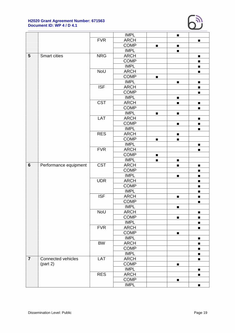
H2020 Grant Agreement Number: 671563 Document ID: WP 4 / D 4.1
Dissemination Level: Public Page 19
IMPL ■
FVR ARCH ■
COMP ■ ■
IMPL ■
5 Smart cities NRG ARCH ■
COMP ■
IMPL ■
NoU ARCH ■
COMP ■
IMPL ■ ■
ISF ARCH ■
COMP ■
IMPL ■
CST ARCH ■ ■
COMP ■
IMPL ■ ■
LAT ARCH ■
COMP ■ ■
IMPL ■
RES ARCH ■
COMP ■ ■
IMPL ■
FVR ARCH ■
COMP ■
IMPL ■ ■
6 Performance equipment CST ARCH ■ ■
COMP ■
IMPL ■ ■
UDR ARCH ■
COMP ■
IMPL ■
ISF ARCH ■ ■
COMP ■
IMPL ■
NoU ARCH ■
COMP ■ ■
IMPL ■
FVR ARCH ■
COMP ■
IMPL ■
BW ARCH ■
COMP ■
IMPL ■
7 Connected vehicles (part 2)
LAT ARCH ■
COMP ■
IMPL ■
RES ARCH ■
COMP ■
IMPL ■
H2020 Grant Agreement Number: 671563 Document ID: WP 4 / D 4.1
Dissemination Level: Public Page 20
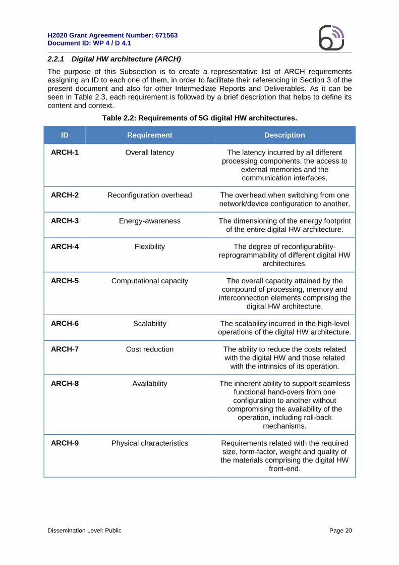
2.2.1 Digital HW architecture (ARCH)
The purpose of this Subsection is to create a representative list of ARCH requirements assigning an ID to each one of them, in order to facilitate their referencing in Section 3 of the present document and also for other Intermediate Reports and Deliverables. As it can be seen in Table 2.3, each requirement is followed by a brief description that helps to define its content and context.
Table 2.2: Requirements of 5G digital HW architectures.
ID Requirement Description
ARCH-1 Overall latency The latency incurred by all different processing components, the access to
external memories and the communication interfaces.
ARCH-2 Reconfiguration overhead The overhead when switching from one network/device configuration to another.
ARCH-3 Energy-awareness The dimensioning of the energy footprint of the entire digital HW architecture.
ARCH-4 Flexibility The degree of reconfigurability-reprogrammability of different digital HW
architectures.
ARCH-5 Computational capacity The overall capacity attained by the compound of processing, memory and
interconnection elements comprising the digital HW architecture.
ARCH-6 Scalability The scalability incurred in the high-level operations of the digital HW architecture.
ARCH-7 Cost reduction The ability to reduce the costs related with the digital HW and those related
with the intrinsics of its operation.
ARCH-8 Availability The inherent ability to support seamless functional hand-overs from one configuration to another without
compromising the availability of the operation, including roll-back
mechanisms.
ARCH-9 Physical characteristics Requirements related with the required size, form-factor, weight and quality of the materials comprising the digital HW
front-end.
H2020 Grant Agreement Number: 671563 Document ID: WP 4 / D 4.1
Dissemination Level: Public Page 21
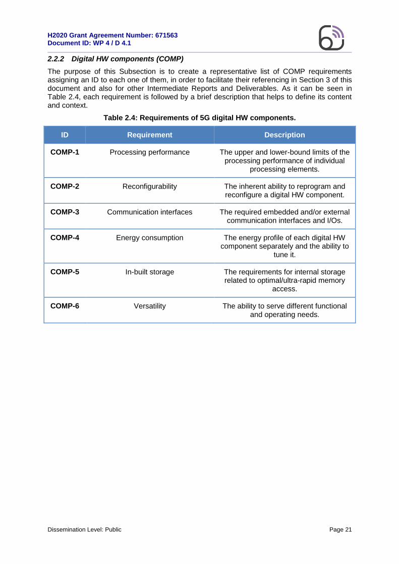
2.2.2 Digital HW components (COMP)
The purpose of this Subsection is to create a representative list of COMP requirements assigning an ID to each one of them, in order to facilitate their referencing in Section 3 of this document and also for other Intermediate Reports and Deliverables. As it can be seen in Table 2.4, each requirement is followed by a brief description that helps to define its content and context.
Table 2.4: Requirements of 5G digital HW components.
ID Requirement Description
COMP-1 Processing performance The upper and lower-bound limits of the processing performance of individual
processing elements.
COMP-2 Reconfigurability The inherent ability to reprogram and reconfigure a digital HW component.
COMP-3 Communication interfaces The required embedded and/or external communication interfaces and I/Os.
COMP-4 Energy consumption The energy profile of each digital HW component separately and the ability to
tune it.
COMP-5 In-built storage The requirements for internal storage related to optimal/ultra-rapid memory
access.
COMP-6 Versatility The ability to serve different functional and operating needs.
H2020 Grant Agreement Number: 671563 Document ID: WP 4 / D 4.1
Dissemination Level: Public Page 22
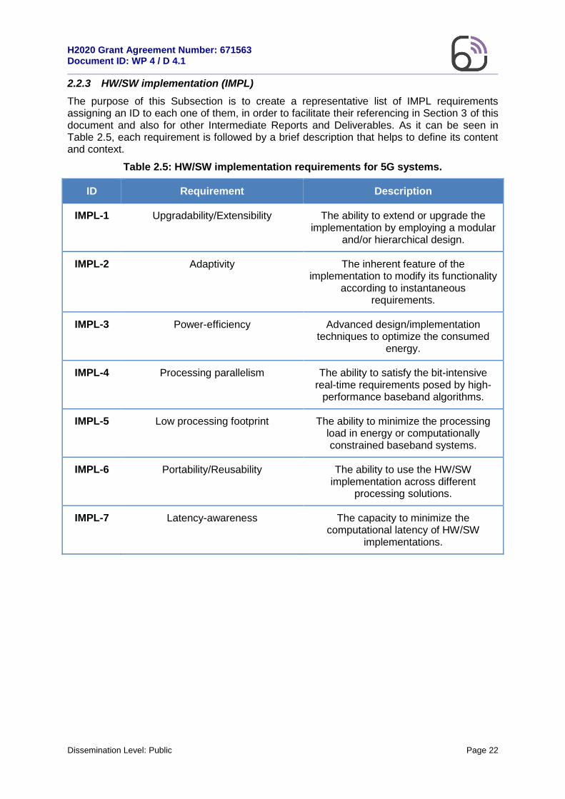
2.2.3 HW/SW implementation (IMPL)
The purpose of this Subsection is to create a representative list of IMPL requirements assigning an ID to each one of them, in order to facilitate their referencing in Section 3 of this document and also for other Intermediate Reports and Deliverables. As it can be seen in Table 2.5, each requirement is followed by a brief description that helps to define its content and context.
Table 2.5: HW/SW implementation requirements for 5G systems.
ID Requirement Description
IMPL-1 Upgradability/Extensibility The ability to extend or upgrade the implementation by employing a modular
and/or hierarchical design.
IMPL-2 Adaptivity The inherent feature of the implementation to modify its functionality
according to instantaneous requirements.
IMPL-3 Power-efficiency Advanced design/implementation techniques to optimize the consumed
energy.
IMPL-4 Processing parallelism The ability to satisfy the bit-intensive real-time requirements posed by high-
performance baseband algorithms.
IMPL-5 Low processing footprint The ability to minimize the processing load in energy or computationally constrained baseband systems.
IMPL-6 Portability/Reusability The ability to use the HW/SW implementation across different
processing solutions.
IMPL-7 Latency-awareness The capacity to minimize the computational latency of HW/SW
implementations.
H2020 Grant Agreement Number: 671563 Document ID: WP 4 / D 4.1
Dissemination Level: Public Page 23
3. Specifications of key concepts in 5G digital baseband processing
3.1 Introduction
5G communications will have to deal with a plethora of services while providing high data capacity and connectivity. In order to provide such a high level of flexibility in applications, several solutions have to be considered from the digital baseband processing perspective. To this respect, representative concepts include capacity increase, spectrum and energy efficiency, flexible reconfiguration, radio co-existence, MIMO techniques, FBMC structures and MTC-related optimizations. Based on the expertise of the partners involved in WP4 and on the UCs (defined in WP1), a number of key concepts have been selected to be implemented and validated in WP4. These concepts were broadly grouped in following two categories:
Digital HW architectures optimising spectrum and energy efficiency (Section 3.2)
Digital HW architectures optimising flexibility (Section 3.3)
The mentioned categories are directly mapped to the tasks T4.2 and T4.3 of the Flex5Gware DoW. These key concepts do not pretend to exhaustively cover the entire 5G digital baseband spectrum. However, they will provide focused innovations at the digital front-end of 5G transceivers. In certain cases, the proposed concepts for the 5G digital HW architectures could either apply to subsection 3.2 or 3.3, but despite this fact the contributions concentrate on one of the broad categories (i.e., a digital HW architecture optimised for spectrum and energy efficiency might also fit the requirements of a digital HW architecture optimised for flexibility and vice versa).
Section 3.2 is divided in three subsections; the first deals with the design, implementation and operating aspects of new 5G waveforms (Section 3.2.1), the second focuses on efficient coding design at low-end and high-end 5G UCs (Section 3.2.2) and the third specifies network-on-chip (NoC) baseband processing architectures able to address major 5G digital HW challenges (Section 3.2.3). In more detail, Section 3.2.1 covers concepts that will study the impact of 5G candidate waveforms on the receiver architecture, especially in respect to efficient HW/SW split of the signal processing components. Effective MIMO equalizer techniques will also be compared. In addition, different architectural structures of FBMC transceivers will be investigated and evaluated towards future 5G mobile cellular networks. In Section 3.2.2 new and versatile routes for the design of low-power / high-throughput LDPC decoders for future generations of mobile cellular networks will be explored. Another concept covers the design of an optimal Turbo-decoder engine able to cope with a large variety of modulation and coding schemes, while limiting the power consumption (to serve IoT devices). Finally in Section 3.2.3 introduces and specifies the design of optimum digital HW processing architectures for 5G network elements that will utilise a high level architecture evaluation design flow. In this context, it is also planned to model and validate receiver algorithms and architectures.
Similarly Section 3.3 specifies techniques for improving modularity and flexibility of the digital HW in 5G transceivers. To that end, flexible partitioning of transceiver functions between HW and SW will be studied using existing HW/SW frameworks (Section 3.3.1). The HW/SW function split will also encompass context awareness functions, (e.g., through the inclusion of sensing devices and the use of network timing and positioning data), which will be seamlessly integrated in the digital HW architectures (Section 3.3.2). In more detail, Section 3.3.1 covers concepts that will focus on the abstraction of transceiver HW blocks and the functional split between HW and SW modules to be supported in 5G programmable terminals. Enhancements to the existing programmable wireless terminal will be done for supporting a novel architecture, devised to efficiently multiplex HW events and simplify the virtualization of non-programmable HW resources. In addition this Section introduces architectural solutions that will foster the partitioning of HW/SW functions targeting 5G software defined networking (SDN) architectures and scenarios. Different processor
H2020 Grant Agreement Number: 671563 Document ID: WP 4 / D 4.1
Dissemination Level: Public Page 24
technologies will be considered ranging from FPGAs, entirely programmable SoCs, general purpose computers (GPCs) and clusters of GPCs. The HW/SW function partitioning deployment approaches will be evaluated by estimating the computational cost, energy overhead and the latencies implied by the HW/SW split. Finally, in this Section it is introduced the concept of dynamic functional split between HW/SW accounting for service requirements, system constraints, and network characteristics for specific WP1 UCs. Section 3.3.2 specifies a comprehensive HW architecture oriented at enhancing modularity and covering in an agnostic way the inclusion of external sensing devices. At the terminal side, an agent and related control able to collect and process the information acquired by sensors will be developed. At the infrastructure side, mechanisms will be investigated for context-dependent radio adaptation, based on the information gathered from deployed sensors. Moreover this Section introduces concepts related to network synchronization and location awareness in mobile networks. The aim is to build and evaluate an architecture that will provide an API for timing and positioning data that can access multiple radio technologies, such that the network can be reconfigured and optimized as requested. In addition, existing methods for characterization of the energy cost will be applied to the internal primitives of the HW to bring energy awareness to the upper layers.
3.1.1 Synergies and collaborations
The envisioned contributions of the different concepts feature complementarities and, up to a certain extent, they share common grounds. This is first reflected in the internal grouping of the different concepts in Sections 3.2 and 3.3. A more concrete testimony of the WP4 collaborations among partners that aim at developing complementary concepts can be seen in the construction of the following PoCs where WP4 partners are contributing:
PoC#5 will demonstrate a full duplex FBMC transceiver and it will bring together CEA and IMC.
PoC#7 will demonstrate HW/SW function split for energy aware communications and it will bring together CTTC and UC3M; this translates to a previous collaboration work that will take place in the context of WP4 and WP5.
PoC#8 will demonstrate a reconfigurable programmable radio platform (terminal side) and SW programming, performed and injected by the network, bringing together CNIT, WINGS, UC3M and TST; this translates to a previous collaboration work that will take place in the context of WP4, WP5.
Furthermore, other collaborations, interactions and synergies among partners could be potentially envisioned considering that a number of stand-alone PoCs will demonstrate features that could complement or augment the work of other WP4 partners:
VTT, F-IAF, CTTC and SEQ will demonstrate a PAPR reduction and power amplifier predistortion solution in the context of PoC#3. Although the development would take place in WP2, the results reported in WP3 might be of interest for a number of WP4 contributors.
NEC will demonstrate a flexible, scalable and reconfigurable small cell platform in the context of PoC#9. The development would take place in WP5. This work could potentially combine with the work of CTTC, CNIT, WINGS and TST in WP4.
TI and UNIPI in the context of PoC#10 will demonstrate a flexible resource allocation scheme in a CRAN/vRAN platform. The development would take place in WP5. As in the previous case, this work could potentially combine with the WP4 work of CTTC, CNIT and WINGS.
Finally, the following concepts specified in WP4 could generate synergies among different partners in WP4 or other WPs:

H2020 Grant Agreement Number: 671563 Document ID: WP 4 / D 4.1
Dissemination Level: Public Page 25
The high-speed low power resilient LDPC decoder that is planned to be developed by CEA at WP4, is a key component that might combine with the work of other WP4 partners such as VTT, CNIT IMC and CTTC.
The power-optimised Turbo-decoder engine for IoT devices developed by SEQ in WP4 could fit the needs and requirements of TST’s work.
The energy profiling measurements conducted by UC3M could be reused (apart from CTTC) by CNIT and TI or even by NEC or UNIPI in WP5.
The modular platform developed by TST might also be of interest for CNIT and TI in WP4 or UNIPI in WP5.
The dynamic reconfiguration controller developed by WINGS might be an interesting concept for CTTC as well.

H2020 Grant Agreement Number: 671563 Document ID: WP 4 / D 4.1
Dissemination Level: Public Page 26
3.2 Digital HW architectures optimising spectrum and energy efficiency
3.2.1 5G waveforms and multi-antenna schemes
3.2.1.1 Implementation of new Waveforms and MIMO Equalization Techniques
There is consensus in the industry and academy that air interface modulation and access schemes, also called waveforms, should be based on multicarrier (MC) with frequency division multiple access (FDMA) or should be a single carrier frequency division multiple access (SC-FDMA) for the 5G mobile networks [And14]. Cyclic prefix orthogonal frequency division multiplexing (CP-OFDM) and SC-FDMA are the current schemes already used in long term evolution (LTE), LTE advanced (LTE-A) and LTE-A Pro. MC-FDMA and SC-FDMA schemes provide the features necessary for fulfilling the requirements of the Flex5GWare UCs.
CP-OFDMA, as a pure MC scheme and CP-OFDM, based on SC-FDMA, provide very elegant solutions for the equalization of transmissions via frequency selective propagation channels. They are elegant in the sense that the implementations of those systems are very simple, in terms of complexity. Especially if a single-antenna, single input single output (SISO), or multiple antennas, MIMO, equalizers and precoders are considered. CP-OFDM utilizes a complex exponential modulation on each subcarrier that is based on the discrete Fourier transform (DFT) and can be efficiently implemented using a fast Fourier transform (FFT). With its efficient implementation, flexibility and multiple access capability, CP-OFDM as it is used in LTE can already fulfil some of the requirements for some of the use-cases in 5G. Since the aim in 5G is to broaden the number of UCs compared to 4G and more challenging KPI values are being introduced, a discussion on alternative or improved MC-FDMA and SC-FDMA schemes has started.
A main drawback of CP-OFDM is the high levels of out-of-band emissions. In DL scenarios, this will limit the total number of subcarriers in a given total bandwidth, which can be efficiently processed in the baseband.
In UL scenarios this imposes a high limitation in the asynchronous transmission of different user's signals. Also in device to device (D2D) scenarios, this could be critical. Either the different users have to be strictly synchronized, limiting flexibility and increasing the control signalling overhead, or a better spectral containment has to be achieved, in order to guarantee a higher spectral efficiency. The main objective of the new proposals, on waveform design is, to provide a better spectral shaping of the transmitted signals, to achieve a better utilization of the expensive spectrum resource.
New proposals for MC and SC-FDMA systems are also based on exponential modulation combined with different levels of pulse shaping/filtering [Ban14]. CP-OFDM has a low complexity pulse shaping employed for each subcarrier: i.e. applying a rectangular filter, with the time duration of one symbol. In practical implementations of CP-OFDM, windowing is applied to the MC/SC blocks before the digital to analogue (DA) conversion to fulfil the out-of-band emissions requirements.
New proposals aim to achieve a better spectral containment compared to conventional CP-OFDM. Therefore, individual or alternative groups of subcarriers are combined and shaped with a more elaborate filter. In the case of a per-subcarrier filtering, the filter that is complex exponentially modulated is usually called prototype filter. Moreover, in some proposals, instead of conventional linear convolution, a cyclic convolution is used. This results in a transmission in blocks longer than the symbol period. Because of the block transmission in those methods, specific measures are needed, such as extra processing power, a guard-band or a CP, to isolate the successive blocks and/or to smoothen the transition between the blocks. This is in some sense similar to what is employed in conventional CP-OFDM in order to reduce the out-of-band radiation.
H2020 Grant Agreement Number: 671563 Document ID: WP 4 / D 4.1
Dissemination Level: Public Page 27
One can classify the advanced MC-FDMA and SC-FDMA proposals according to three basic
aspects:
Pulse shaping/filtering on a per subcarrier basis or on the basis of a group of
subcarriers
Linear or cyclic convolution based pulse shaping/filtering
Guard interval/CP/windowing based or block overlapping based systems
It is important to note that, conventional CP-OFDM as employed in LTE could also be classified into all these categories. If we assume that a trivial pulse shaping is done per subcarrier, using a linear convolution, a CP and a time window are necessary. FBMC/ offset quadrature amplitude modulation (OQAM) or FBMC/QAM systems can be classified in the category of linear filtering on a per sub-carrier basis with block overlapping. Filtered CP-OFDM systems, universal filtered MC (UFMC) or UF-OFDM, combine classical CP-OFDM with FBMC by filtering groups of subcarriers. For example, one or a group of resource blocks (sub-channels) are filtered to reduce the out-of-band emissions. Linear convolution is employed and a guard interval is necessary in the sub channel level. Generalised frequency division multiplexing (GFDM) systems employ a per-subcarrier filtering using cyclic convolution, a CP is added and windowing is necessary. Similarly, windowed CP-circular OQAM (WCP-COQAM) also utilizes a per-subcarrier filtering with cyclic convolution, and a CP and windowing. DFT spread OFDM is a combination of pre-processing of the subcarriers and OFDM, thus it can be similarly classified in the same way as CP-OFDM.
All these newly proposed waveforms have the possibility to be realized using different structures. For example, FBMC/OQAM systems have the possibility to be implemented using a time or a frequency domain filtering of each subcarrier. In the case of a time domain filtering, after the FFT with a length equal to the number of subcarriers, a polyphase decomposition of the prototype filter is employed and different possibilities exist to realize them. The polyphase components of the prototype filter can be realized in direct form, as lattice rotations or lifting steps. In the case of lattice rotations or lifting steps, practical multiplier-less filtering is possible, by coarse coefficient quantization or coordinate rotation digital computer (CORDIC) steps. The polyphase decomposition based structure provides full flexibility in the choice of the prototype filter, its length and also the length of the per-subcarrier linear equalizes. Another possibility is the filtering in the frequency domain, where the prototype coefficients have to be chosen in a specific way to allow low complexity implementation [Bel01]. In this structure a longer FFT is applied and its length has to be equal to the filter length and, after coefficient multiplication in the frequency domain, smaller inverse FFTs (IFFTs) are needed to recover the subcarrier signals. It should be understood, that the size of the FFTs is chosen in a way that a linear convolution is still performed in a fashion, similar to the well-known methods of overlap-and-add and overlap-and-save methods. Frequency domain filtering is sometimes also called fast-convolution (FC) or frequency spread based FBMC/OQAM. Also for f-OFDM or UFMC there are similar time and frequency domain implementations, to realize the filtering of groups of subcarriers.
From the possibility of realizing the linear convolution in the frequency domain, with the help of multiple FFTs of different sizes, it becomes clear that also a cyclic convolution can also be implemented in a similar way. But now the requirements for linear convolution, e.g. the FFT size is too small compared to the prototype filter length, are not fulfilled. Based on this principle, efficient structures also exist for GFDM and WCP-COQAM implementations.
We can conclude that a major building block for the implementation of the MC waveforms is the FFT. In most of the waveforms, FFTs of different sizes are necessary, and their size may even vary for different use-cases. Both frequency domain filtering and time domain windowing are similar operations since only a block multiplication is performed and no convolution. If time-domain filtering is implemented, linear convolution in the time domain can
H2020 Grant Agreement Number: 671563 Document ID: WP 4 / D 4.1
Dissemination Level: Public Page 28
be employed, because the polyphase components lengths are usually too short for a fast convolution method to be efficient.
Basically, the implementation of the 5G proposed waveforms, requires functional blocks, using FFTs and filtering/sum-of-products functions. The signal generation complexity of new waveforms, and the reception of them, is basically defined by the level of required flexibility, cost, energy efficiency and data volume by each use case. In principle, all Flex5Gware UCs can be considered here, if we take into account their essential KPIs and search for the proper architecture to optimize them.
On top of the waveform generation and demodulation, comes the SISO or MIMO processing, equalization or precoding, to recover or to precode the symbols to compensate for the transmission channel, to improve signal-to-interference-plus-noise ratio (SINR) or to improve the spectral efficiency by means of spatial multiplexing. The complexity of these modules clearly depends on the architecture chosen for each waveform generation/reception. The architecture of the system will be based on building blocks implemented in HW and SW. Some of the basic and frequently reused building blocks, e.g. the FFT or filtering/windowing, can be implemented in HW or partially in HW and partially in SW. Design and implementation of equalizers and pre-coders is usually done in SW.
In Flex5Gware the different 5G waveform proposals will be analyzed, especially from a complexity perspective. The different architectures for the above mentioned waveforms need to be carefully evaluated regarding the various requirements of the Flex5Gware UCs. Their impact on a UE is particularly important, because of the variety of equipment expected to coexist. The architecture chosen for a UE used in MTC with low capacity batteries and low rate requirements can be different to the one for high-end equipment with high capacity batteries and high rate requirements. Different algorithms employed in MIMO processing also provide different levels of complexity, power consumption, SINR levels and performance. For the UCs defined in Flex5GWare, where specific scenarios include MIMO processing, a detailed comparison needs to be performed by taking mainly complexity and performance into account.
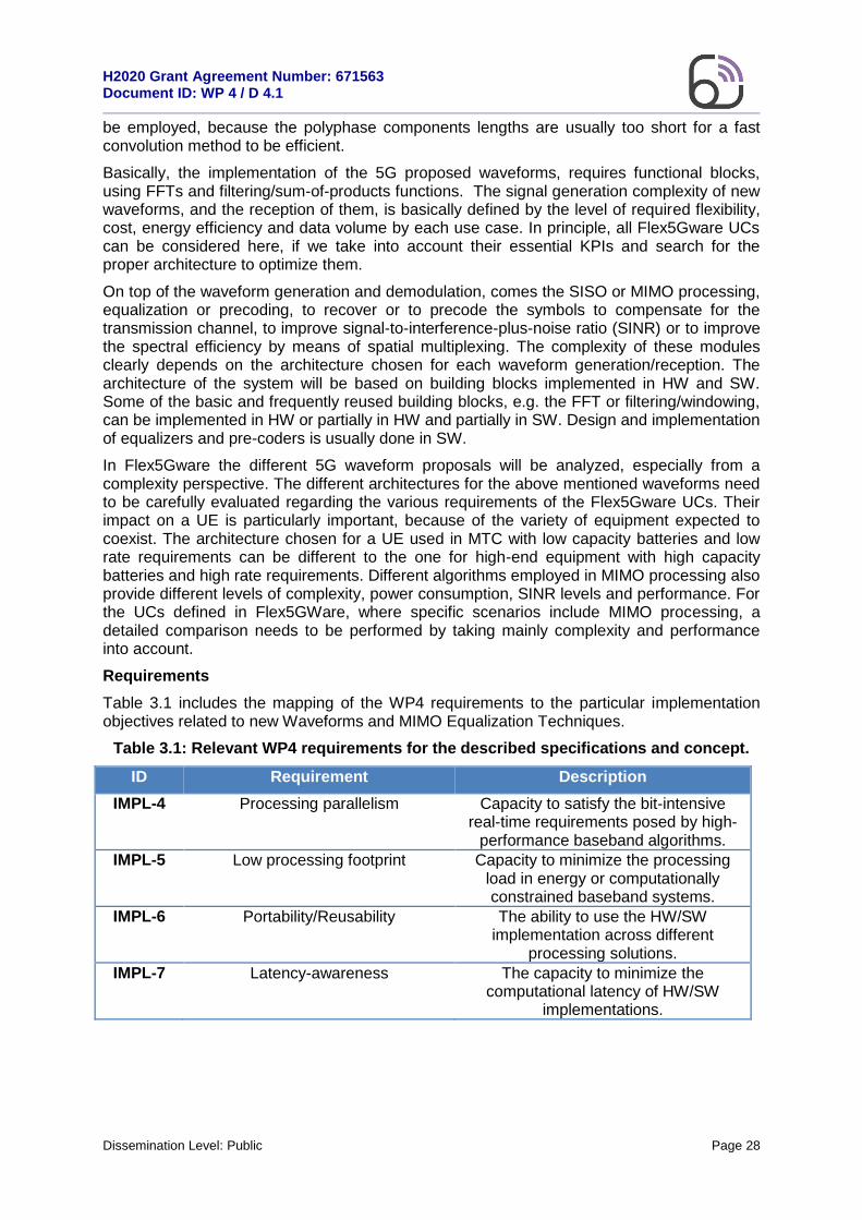
Requirements
Table 3.1 includes the mapping of the WP4 requirements to the particular implementation objectives related to new Waveforms and MIMO Equalization Techniques.
Table 3.1: Relevant WP4 requirements for the described specifications and concept.
ID Requirement Description
IMPL-4 Processing parallelism Capacity to satisfy the bit-intensive real-time requirements posed by high-
performance baseband algorithms.
IMPL-5 Low processing footprint Capacity to minimize the processing load in energy or computationally constrained baseband systems.
IMPL-6 Portability/Reusability The ability to use the HW/SW implementation across different
processing solutions.
IMPL-7 Latency-awareness The capacity to minimize the computational latency of HW/SW
implementations.
H2020 Grant Agreement Number: 671563 Document ID: WP 4 / D 4.1
Dissemination Level: Public Page 29
3.2.1.2 FBMC structures for 5G
So far, the appetite for broadband service has fuelled the development of mobile cellular networks. Mobile communications started with wireless real time voice communications in the first and second generations of cellular systems (1G and 2G) to provide reliable voice connectivity everywhere. It was then followed by internet data connectivity in the third generation (3G) when the adoption of laptop computers became widespread to bring internet on-the-go. Finally, the advent of the smart-phone accelerated the demand for high bandwidth with the world information accessed at the tip of everyone's finger everywhere at any time. Therefore, the aim to deliver high-bandwidth pipes has logically been the main driver for the current fourth generation (4G) also called LTE and LTE-A.
In order to maximize spectral efficiency, strict synchronization and orthogonality between users within a single cell is imposed by LTE and LTE-A standards. However, sporadic traffic has emerged as an important service for future generations of cellular networks (5G). MTC devices of the Internet of Things are expected to inherently generate sporadic data traffic to the network and should not be forced to be integrated into the constrained synchronization procedure of LTE-A in order to limit signalling overhead. Furthermore, a previously unforeseen mechanism designed to save battery usage of the handset, also called fast dormancy, resulted in a significant control signalling growth. This mechanism causes the UE to go into a deep sleep mode and break any connection to the network. When the UE changes back to an active state the mobile has to go through a complete synchronization procedure again. This phenomenon is another significant source of sporadic traffic on the network [Wun14].
Furthermore, because spectrum is scarce and expensive, its utilization should be as optimal as possible. However, the nature of the sporadic traffic causes significant fragmentation. Therefore carrier aggregation will be implemented to achieve much higher rates by variably aggregating non-contiguous frequency bands [Wun13]. The legacy LTE-A waveform imposes generous guard bands to other legacy networks to satisfy spectral mask requirements.
Therefore relaxed synchronization and access to fragmented spectrum have been considered as key parameters for future generations of wireless networks [Wun14] and [Wun13]. This requirement of spectrum agility has encouraged the study of alternative multicarrier waveforms such as FBMC to provide better adjacent channel leakage performance without compromising spectral efficiency [Dor14].
Furthermore, few studies have been realized to evaluate the feasibility of hardware prototyping of FBMC transceiver. In [Dzi14], an implementation on Software Defined Radio platform has been done. In [Nad14], a complete design and prototyping flow from algorithm specification to on-board validation and demonstration have been shown in the context of FBMC for 5G. One of the most advanced concept was illustrated in [Ber14] in which real time non-synchronous mulituser IP over-the-air transmission on fragmented spectrum has been demonstrated. All these works have demonstrated the feasibility of the prototyping of FBMC transceiver with manageable complexity on today-platform. However, as previously mentioned, one of the future challenges will be the coexistence of legacy systems (e.g. LTE) with new waveforms (one or more) adapted to new scenarios with an unified transceiver architecture. The object of this study is to propose an architecture of implementation suitable for very large scale integration (VLSI) targets such as field programmable gate arrays (FPGAs) or application specific integrated circuits (ASICs)) that could support both OFDM and FBMC receivers.
A unified frame structure
In order to provide a uniform service experience to users with the premises of heterogeneous networking but also higher data rates, [Wun14] introduced the concept of the unified frame structure for 5G. The idea is to provide a flexible multi-service solution in an integrated air
H2020 Grant Agreement Number: 671563 Document ID: WP 4 / D 4.1
Dissemination Level: Public Page 30
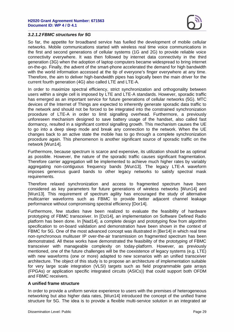
interface. A frame, divided into different areas of services has been proposed. Four types of traffic have been devised to allow for flexible operation. An example of the proposed frame is shown in Figure 3.1: type I and II represent high data rate traffic for video or other high bandwidth services; type I possibly also carries real-time traffic. Type III and IV are dedicated to sporadic asynchronous MTC traffic. Different levels of traffic scheduling have thus been considered: strictly scheduled and organized traffic as already in place in LTE and LTE-A is dedicated to high bandwidth data pipes, while sporadic traffic uses contention-like based approaches with random access designed to efficiently enable MTC type payloads (Type III and IV) and bring an efficient solution to the fast dormancy issue.
Figure 3.1: 5G Unified Frame Structure proposed by [Wun14].
In order to be efficient, this structure clearly demands to revisit the strict synchronism and orthogonality that prevails in current LTE-A systems. This new requirement led to rethink the transmission technique and consequently the transceiver structure of the 5th generation of cellular networks.
Alternative waveforms such as UFMC [Vak13], GFDM [Fet09] and FBMC have thus been considered. The motivation of the new waveforms is to keep the flexibility of multicarrier modulation, while the frequency response of each carrier is controlled by introducing a filter bank centered on every active carrier and based on the same prototype response. This prototype filter can be selected to minimize (null) adjacent channel interference. As the filtering is embedded in the digital modulation no additional filter is required and more flexibility is obtained.
When considering the unified frame structure, a mix of synchronous (high data rate pipe) and asynchronous traffic should coexist. This 5G scenario, could be solved by considering legacy waveforms (i.e.: OFDM) for structured synchronous traffic and flexible asynchronous (i.e. FBMC) for more sporadic traffic. We then propose to investigate an architecture of implementation suitable to VLSI targets (FPGA, ASIC) that could support both OFDM and FBMC receivers.
OFDM receiver architecture
The definition of OFDM architectures has been widely investigated in the literature [Spe99]. A typical architecture of OFDM receiver is depicted in Figure 3.2.

H2020 Grant Agreement Number: 671563 Document ID: WP 4 / D 4.1
Dissemination Level: Public Page 31
Figure 3.2: Typical OFDM receiver block diagram
Based on a synchronization performed by the time domain (TD) synchronization module, a
FFT of size N is processed in blocks of GINN samples generating N points, where GIN
is the size of the guard interval. The TD synchronization module optimally localizes the FFT
window. Successive N point blocks are stored in a memory unit. The memory unit buffers
the data for later processing. In parallel, a frequency domain synchronization detector estimates the carrier frequency offset (CFO) at the output of the FFT.
On the channel estimation datapath, CFO compensation is first performed in the frequency domain using a feed-forward approach. Then, channel coefficients are estimated on the pilot subcarriers before being interpolated for every active subcarrier. Once the channel is estimated on all the active subcarriers the response is stored in a dedicated channel response memory. Depending on the pilot carrier distribution within the time frequency grid, a time interpolation can also be performed. The data buffered in the memory unit are then processed through an one-tap per subcarrier equalizer. Demapping and Log-Likelihood Ratio (LLR) computation complete the inner receiver architecture. Soft-input FEC decoders finally recover the originally sent messages.
FBMC Receivers
A multicarrier system can be described by a synthesis/analysis filter bank, i.e. a transmultiplexer structure. The synthesis filter bank is composed of a set of parallel transmit filters. FBMC waveforms utilize a prototype filter design to give a good frequency localization of the subcarriers. The considered prototype filter is based on the frequency sampling technique of PHYDYAS2 [Bel01]. This technique gives the advantage of using a closed-form representation that includes only a few adjustable design parameters.
The most significant parameter is the duration of the impulse response of the prototype filter
also called overlapping factor, K . The impulse response of the prototype filter is given by [Bel01]:
2 PHYDYAS “FP7 European project - phydyas: physical layer for dynamic spectrum access and cognitive radio”, http://www.phydyas-ict.org.

H2020 Grant Agreement Number: 671563 Document ID: WP 4 / D 4.1
Dissemination Level: Public Page 32
12
)(12(0)=)(1
1=
tKN
kcoskGGth P
kK
k
P
(1)
where
2(1)1,
2
1,0.971959831,=(0..3) PP GG for an overlapping factor of 4=K and N
is the number of carriers. The larger the overlapping factor K , the more localized the signal will be in frequency. Adjacent carriers significantly overlap with this kind of filtering. In order to keep adjacent carriers orthogonal, real and pure imaginary values alternate on successive carrier frequencies and on successive transmitted symbols (Offset-QAM modulation is used) for a given carrier at the transmitter side. The well-adjusted frequency localization of the prototype filter guarantees that only adjacent carriers interfere with each other. This allows for a more flexible operation than OFDM for FDMA, i.e.: non synchronous flexible frequency division multiple access.
Most of the published receivers are PolyPhase Network (PPN) based receivers [Bel01]. In this scheme, the filtering process is realized in the time domain before the FFT. This reduces the size of the FFT and therefore its complexity but makes the receiver less tolerant to large channel delay spread or synchronization mismatch of the FFT. Therefore, this strategy is not well adapted to non synchronous multiuser scenarios. In [Dor14], the authors describe a high performance receiver architecture denoted FS-FBMC (frequency spreading FBMC). One advantage of this architecture is that frequency domain time synchronization may be performed independently of the position of the FFT [Dor14]. This is realized by combining timing synchronization with channel equalization. Moreover, good performance for channel exhibiting large delay spread is achieved. This asynchronous frequency domain processing of the receiver provides a receiver architecture that allows for multiuser asynchronous reception and is particularly adapted to the envisaged scenarios.
FBMC waveforms could give benefits in comparison to OFDM when dynamic spectrum access and relaxed synchronization between users is considered. Therefore, an asynchronous FBMC receiver should be able to fully exploit these benefits if the signal is efficiently demodulated in the frequency domain without a priori knowledge of the FFT timing alignment (i.e. the location of the FFT block, a property called asynchronous FFT) [Ber14]. A FBMC receiver architecture based on this assumption is depicted in Figure 3.3. An
asynchronous FFT of size KN is processed every blocks of /2N samples generating KN
points, i.e. if mr is the thm received vector, a KN -point FFT is computed for samples
/2)(= Nmnk with 1,0,1,= NKn . These successive KN points are stored in a
memory unit. The memory unit buffers the data for later processing. In parallel a frequency domain synchronization detector detects the start of burst and estimates CFO directly at the output of the FFT. Once a start of burst is detected, CFO is estimated on the reference signal. On the channel estimation datapath, CFO compensation is first performed in the frequency domain using a feed-forward approach. Then, as in OFDM, channel coefficients are estimated on the pilot subcarriers before being interpolated for every active subcarrier. Once the channel is estimated on all the active subcarriers the response is stored for each user in a dedicated channel response memory. The data buffered in the memory unit are then processed through a one-tap per subcarrier equalizer before filtering by the FBMC prototype filter which is similar to OFDM receiver. Demapping and LLR computation complete the inner receiver architecture. As far as the LLR computation for FBMC, processing are a bit different. Indeed, in case of FS-based receiver, the computation of the
LLR associated to a bit from an observation symbol is a function of 12 K channel coefficients [Dor14], making the LLR computation module slightly more complex. However it should be mentioned that the complexity of the processing is in the same order of magnitude than LLR computation in case of precoded OFDM scheme such as the LTE uplink scheme.

H2020 Grant Agreement Number: 671563 Document ID: WP 4 / D 4.1
Dissemination Level: Public Page 33
Figure 3.3: Typical FBMC receiver block diagram [Ber14].
The choice of multicarrier modulations parameters depends on the propagation channel and
for LTE (10MHz band) the frequency spacing is set to 15 kHz, the FFT size is equal to 1024
points and consequently the sampling frequency is equal to 15.36 MHz (a multiple of
universal mobile telecommunications system (UMTS) chip rate) and the guard interval is 72
samples ( 4.7GIT s). For FS-FBMC a choice of 4=K has proven efficient for adjacent
channel leakage rejection [Dor14], and in this case 256=N can sustain channel delay
spreads of the same level as the LTE 10MHz OFDM case. 1024=N would consider similar
carrier spacing (15 kHz).
A Unified Architecture for FBMC and OFDM
Based on the previous results, and keeping in mind that the aim of a flexible receiver that supports both legacy LTE and future 5G waveform, we propose to analyse design considerations of the next generation of FBMC and OFDM receivers. The proposed unified architecture is depicted Figure 3.4.
The system comprises of essentially the receiver (RX) processing chain. Layer 2/3 processing could be made on an application processor connected through the Higher layer bus. This processor will perform functions such as MAC, Packet Data Convergence Protocol (PDCP), Radio Link Control (RLC) and Radio Resource Management (RRM). Control processing for the RX could also be performed on the application processor; this function provides low level real-time control.
Concerning the receiver architecture itself, a generic and flexible digital front end conditions the signal and gives to the next processing blocks a signal sampled at the critical frequency. The time domain signal is transformed in a frequency domain signal by the use of a FFT processing engine.
H2020 Grant Agreement Number: 671563 Document ID: WP 4 / D 4.1
Dissemination Level: Public Page 34
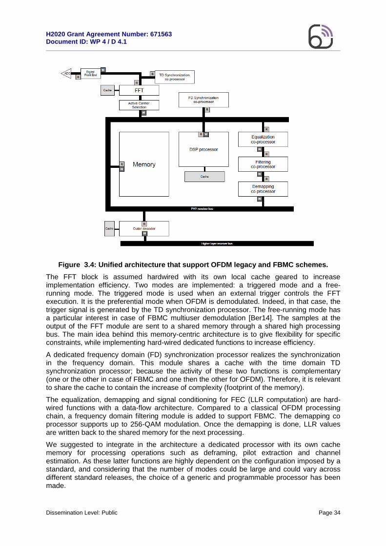
Figure 3.4: Unified architecture that support OFDM legacy and FBMC schemes.
The FFT block is assumed hardwired with its own local cache geared to increase implementation efficiency. Two modes are implemented: a triggered mode and a free-running mode. The triggered mode is used when an external trigger controls the FFT execution. It is the preferential mode when OFDM is demodulated. Indeed, in that case, the trigger signal is generated by the TD synchronization processor. The free-running mode has a particular interest in case of FBMC multiuser demodulation [Ber14]. The samples at the output of the FFT module are sent to a shared memory through a shared high processing bus. The main idea behind this memory-centric architecture is to give flexibility for specific constraints, while implementing hard-wired dedicated functions to increase efficiency.
A dedicated frequency domain (FD) synchronization processor realizes the synchronization in the frequency domain. This module shares a cache with the time domain TD synchronization processor; because the activity of these two functions is complementary (one or the other in case of FBMC and one then the other for OFDM). Therefore, it is relevant to share the cache to contain the increase of complexity (footprint of the memory).
The equalization, demapping and signal conditioning for FEC (LLR computation) are hard- wired functions with a data-flow architecture. Compared to a classical OFDM processing chain, a frequency domain filtering module is added to support FBMC. The demapping co processor supports up to 256-QAM modulation. Once the demapping is done, LLR values are written back to the shared memory for the next processing.
We suggested to integrate in the architecture a dedicated processor with its own cache memory for processing operations such as deframing, pilot extraction and channel estimation. As these latter functions are highly dependent on the configuration imposed by a standard, and considering that the number of modes could be large and could vary across different standard releases, the choice of a generic and programmable processor has been made.
H2020 Grant Agreement Number: 671563 Document ID: WP 4 / D 4.1
Dissemination Level: Public Page 35
Eventually, a specific outer module is implemented. A Read Write interface is allowed to benefit of the shared memory for the rate matching and interleaving process. Cache memory is attached especially for the FEC (e.g Turbo decoder). As previously mentioned, the output of the outer decoder is sent to a bus connected to a processor in charge of higher layer functions.
One major limitation of such an architecture comes from the throughput constraints that are put on memory access through the data bus.
Memory bus specification
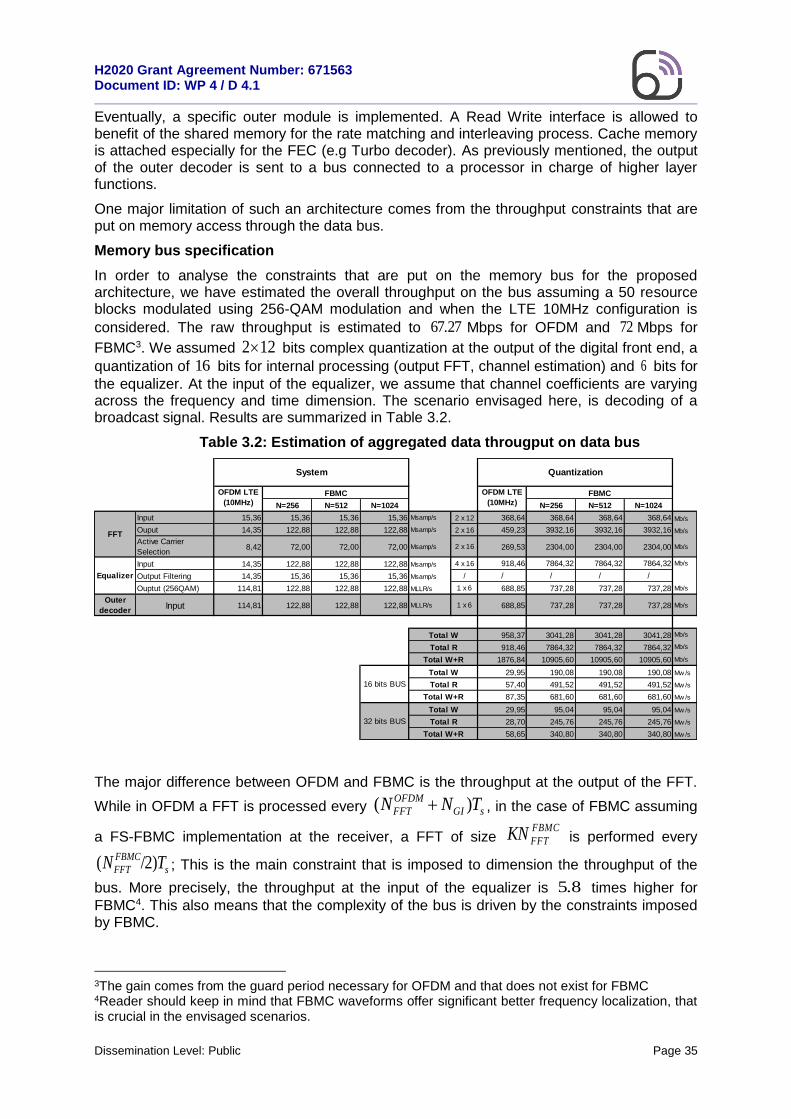
In order to analyse the constraints that are put on the memory bus for the proposed architecture, we have estimated the overall throughput on the bus assuming a 50 resource blocks modulated using 256-QAM modulation and when the LTE 10MHz configuration is
considered. The raw throughput is estimated to 67.27 Mbps for OFDM and 72 Mbps for
FBMC3. We assumed 122 bits complex quantization at the output of the digital front end, a
quantization of 16 bits for internal processing (output FFT, channel estimation) and 6 bits for
the equalizer. At the input of the equalizer, we assume that channel coefficients are varying across the frequency and time dimension. The scenario envisaged here, is decoding of a broadcast signal. Results are summarized in Table 3.2.
Table 3.2: Estimation of aggregated data througput on data bus
The major difference between OFDM and FBMC is the throughput at the output of the FFT.
While in OFDM a FFT is processed every sGI
OFDM
FFT TNN )( , in the case of FBMC assuming
a FS-FBMC implementation at the receiver, a FFT of size FBMC
FFTKN is performed every
s
FBMC
FFT TN /2)( ; This is the main constraint that is imposed to dimension the throughput of the
bus. More precisely, the throughput at the input of the equalizer is 5.8 times higher for
FBMC4. This also means that the complexity of the bus is driven by the constraints imposed by FBMC.
3The gain comes from the guard period necessary for OFDM and that does not exist for FBMC 4Reader should keep in mind that FBMC waveforms offer significant better frequency localization, that is crucial in the envisaged scenarios.
N=256 N=512 N=1024 N=256 N=512 N=1024
Input 15,36 15,36 15,36 15,36 Msamp/s 2 x 12 368,64 368,64 368,64 368,64 Mb/s
Ouput 14,35 122,88 122,88 122,88 Msamp/s 2 x 16 459,23 3932,16 3932,16 3932,16 Mb/s
Active Carrier
Selection8,42 72,00 72,00 72,00 Msamp/s 2 x 16 269,53 2304,00 2304,00 2304,00 Mb/s
Input 14,35 122,88 122,88 122,88 Msamp/s 4 x 16 918,46 7864,32 7864,32 7864,32 Mb/s
Output Filtering 14,35 15,36 15,36 15,36 Msamp/s / / / / /
Ouptut (256QAM) 114,81 122,88 122,88 122,88 MLLR/s 1 x 6 688,85 737,28 737,28 737,28 Mb/s
Outer
decoderInput 114,81 122,88 122,88 122,88 MLLR/s 1 x 6 688,85 737,28 737,28 737,28 Mb/s
958,37 3041,28 3041,28 3041,28 Mb/s
918,46 7864,32 7864,32 7864,32 Mb/s
1876,84 10905,60 10905,60 10905,60 Mb/s
16 29,95 190,08 190,08 190,08 Mw /s
57,40 491,52 491,52 491,52 Mw /s
87,35 681,60 681,60 681,60 Mw /s
32 29,95 95,04 95,04 95,04 Mw /s
28,70 245,76 245,76 245,76 Mw /s
58,65 340,80 340,80 340,80 Mw /s
FFT
Equalizer
OFDM LTE
(10MHz)FBMC
System Quantization
Total W
Total R
Total W
OFDM LTE
(10MHz)FBMC
Total W+R
Total W
Total R
Total W+R
16 bits BUS
Total W+R
32 bits BUS
Total R
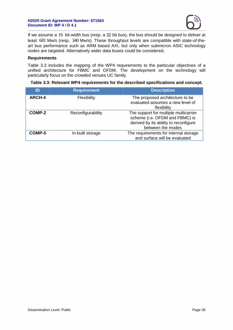
H2020 Grant Agreement Number: 671563 Document ID: WP 4 / D 4.1
Dissemination Level: Public Page 36
If we assume a 16 bit-width bus (resp. a 32 bit bus), the bus should be designed to deliver at
least 681 Mw/s (resp. 340 Mw/s). These throughput levels are compatible with state-of-the-
art bus performance such as ARM based AXI, but only when submicron ASIC technology nodes are targeted. Alternatively wider data buses could be considered.
Requirements
Table 3.3 includes the mapping of the WP4 requirements to the particular objectives of a unified architecture for FBMC and OFDM. The development on the technology will particularly focus on the crowded venues UC family.
Table 3.3: Relevant WP4 requirements for the described specifications and concept.
ID Requirement Description
ARCH-4 Flexibility The proposed architecture to be evaluated assumes a new level of
flexibility
COMP-2 Reconfigurability The support for multiple multicarrier scheme (i.e. OFDM and FBMC) is derived by its ability to reconfigure
between the modes
COMP-5 In-built storage The requirements for internal storage and surface will be evaluated

H2020 Grant Agreement Number: 671563 Document ID: WP 4 / D 4.1
Dissemination Level: Public Page 37
3.2.2 Coding solutions for 5G
3.2.2.1 Efficient high performance LDPC decoding
LDPC codes and Message-Passing decoding
The invention of low density parity check (LDPC) codes by Gallager in the early 60’s [Gal63] is widely recognized as one of the most significant contributions to coding theory. Yet, rather than a family of codes, Gallager invented a new method of decoding linear codes, by using iterative message-passing (MP) algorithms. The capability of MP decoding algorithms to deal with long codes opened the way to Shannon limit. They led to the development of graph-based codes and belief-propagation decoding, closely related to the probabilistic approach to coding devised by Shannon. Nowadays, LDPC codes are known to be capacity approaching codes for a wide range of channel models [Ric01], which motivated the increased interest of the scientific community over the last 15 years and supported the rapid transfer of this technology to the industrial sector.
Despite the aforementioned advantages, LDPC codes did not meet with immediate success from the scientific community. The main reason is that MP decoding algorithms were considered “impractical to implement” when LDPC codes were invented in the early 60’s. This explains why they have been somehow “neglected” for more than three decades, and “rediscovered” in the late 90’s, after the power of iterative decoding techniques had also been confirmed by the discovery of Turbo-codes. Presently, FEC mechanisms used in modern communication systems rely mostly on LDPC codes – used in 802.11n (Wi-Fi), 802.16e (WiMAX), 802.15.3c (WPAN), and several DVB standards – and Turbo codes – used in the 3rd generation partnership project (3GPP) and LTE.
Due to the remarkable progress in the VLSI technology, MP decoding has also become over the last years synonymous with practical solutions for flexible and cost effective hardware designs. Message-passing architectures have been abstracted in the VLSI-theory literature [Len90] by a model that closely resembles MP decoding. The architecture is composed of processing units (PUs) that perform the desired computation by passing messages to each other. In this way, a PU may access the information computed by or stored in the register of another PU. The way such architecture applies to LDPC decoding is closely related to the bipartite graph representation of LDPC codes [Tan81]. Indeed, a LDPC code can be conveniently represented by a sparse bipartite graph comprising two types of nodes, known as variable-nodes and check-nodes, connected by edges: each variable-node corresponds to a bit of the LDPC codeword, while each check-node corresponds to a parity-check on the bits it is connected to. Accordingly, an LDPC decoder comprises two types of PUs, namely variable-node units (VNUs) and check-node units (CNUs). Messages are passed between VNUs and CNUs, in both directions, along the edges of the bipartite graph.
In a fully parallel architecture, a dedicated processing unit is instantiated in hardware for each node of the bipartite graph, and connected through an interconnect network [Bou14]. While this architecture guarantees the maximum degree of parallelism, thus optimizing the decoding throughput, it is scarcely used in practical implementations, because (i) it requires a very large and complex interconnect network, which may cause routing congestions and consumes a significant amount of silicon area and power, and (ii) it does not provide any flexibility, as it is dedicated to a single specific code. At the opposite design spectrum, serial architectures employ only one VNU and one CNU, which are then reused to process all the variable- and check-nodes of the bipartite graph. Message passing is implemented by storing the computed messages in a dedicated memory, and reading them from the memory whenever they are needed by another processing unit. Serial architectures provide very good flexibility and can support a large variety of codes. However, flexibility comes at the price of decreased decoding throughput, which may be way too low for most practical applications.
The partially parallel architecture inherits the main features and advantages of the two aforementioned architectures. In the partially parallel architecture, the number of VNUs and
H2020 Grant Agreement Number: 671563 Document ID: WP 4 / D 4.1
Dissemination Level: Public Page 38
CNUs instantiated in hardware is lower than the number of variable and check nodes, and multiple nodes share a same processing unit. Different trade-offs between areas, throughput and flexibility can be obtained by adjusting the number of processing units. Moreover, structured LDPC codes (e.g., Quasi-Cyclic LDPC [Fos04]) have been largely adopted in order to reduce the complexity of the interconnection network. For such codes, the set of check-nodes can be partitioned into several subsets, known as layers, such that any variable-node is connected to at most one check-node in each layer. Check-nodes within one layer are processed in parallel, by instantiating in hardware the corresponding number of CNUs. Messages computed by the CNUs are immediately passed to the corresponding VNUs, which are then updated before the next layer of check-nodes is processed. This message scheduling, known as layered scheduling, propagates information faster and converges in about half the number of iterations compared to the fully parallel scheduling, thus yielding a lower decoding latency. Due to its benefits in terms of area/throughput/flexibility, the partially parallel layered decoder has been widely adopted, and can be considered as a de facto standard solution in most applications [Bou14].
Cost-effective, high-throughput and low-power designs
Cost (area) minimization has been traditionally considered as the most important target to achieve in the design of complex baseband processing components. However, with the advent of ultra-deep submicron CMOS technologies, substantial cost reductions have been made possible by the increase in density integration. Therefore, area efficiency is no longer the main objective, and design challenges move towards new application-driven objectives, as throughput and power consumption. Cost, throughput and power optimisations mainly rely on architectural choices. The choice of the hardware architecture (fully parallel, partially parallel, or serial) is one of them. The parallelization degree of the partially parallel architecture (i.e., the number of processing units instantiated in hardware) is another. Further optimisations can be obtained by considering different processing unit architectures, e.g., implementing different decoding algorithms or processing the input data in either a serial or a parallel manner [Bon14]. One possible way to achieve even higher throughput is to unroll hardware resources, i.e. to instantiate dedicated hardware for each iteration and then pipeline such hardware [Sch13]. Unrolling HW resources further increases the throughput, at the price of a significant increase in the area. Low-power optimisations have also been proposed, based either on an interconnect-driven code design approach to eliminate the need for a complex interconnection network [Man02, Dar08], or on the early detection of the iterative decoding’s convergence, to terminate the computations, thereby reducing dynamic power [Dar08].
Figure 3 shows different trade-offs between throughput and energy consumption for state-of-the-art ASIC designs of LDPC decoders in different technology nodes. Throughput is reported normalized to area, while the energy consumed is reported per coded bit. Values reported in subfigure A correspond to those obtained for the original technology point (shown in the legend), while values reported in subfigure B have been scaled to 28 nm technology (precisely, values reported in subfigure B have been derived after first scaling both area and power to 28 nm). It is worth noting that values reported after technology scaling are approximate, and may vary in a real case scenario. Also, the LDPC decoders presented in Figure 3 are based on different algorithms and may have different error correction capabilities. After technology scaling, the best trade-off is achieved by the ultra-high throughput architecture proposed in [Sch13]; this architecture is based on hardware unrolling, and achieves a throughput of 160 Gbps, while consuming an area of 12mm2 (in 65 nm technology).

H2020 Grant Agreement Number: 671563 Document ID: WP 4 / D 4.1
Dissemination Level: Public Page 39
Figure 3.5: Throughput vs. energy consumption trade-offs for state-of-the-art ASIC designs.
Proposed approach to cost-effective, high-throughput, and low-power optimisations
In Flex5Gware, we address the design of cost-effective LDPC decoders, suitable for the new generation of communication systems, requiring increased data rates and reduced energy footprint. Our approach is to integrate imprecision mechanisms for message computing and storage in LDPC decoders, which is seen as an enabler for cost-effective, high-throughput, and/or low-power optimisations. Practical hardware implementations of LDPC decoders are mainly based on the min-sum (MS) algorithm or enhanced versions of it, such as normalized MS (NMS) and offset MS (OMS) [Sav14]. One advantage of MS-based decoding algorithms is that processing units can be implemented with very simple arithmetic and logic operations, such as adders for the VNU, and XOR-gates and comparators for the CNU. A preliminary work on the design of MS-based LDPC decoders using imprecise arithmetic has been presented in [Kam13]. The approach consists in using imprecise arithmetic operators (adders and comparators), obtained by pruning the circuit of the precise operator. This amounts to optimising the design performance by removing a certain number of logic gates from the processing units, in such a way that the decoder is still able to perform reliable error correction. Two imprecise variants of the OMS decoding have also been recently proposed in [Ngu15]. They have been shown to allow significant reduction in the memory (25% with respect to the baseline) and interconnect, along with a throughput increase of 28% with respect to the OMS decoder. They also provide excellent error correction performance, close to the original OMS decoder, despite the impreciseness introduced in the processing units.
It is worth noting that one important characteristic of LDPC decoders is that the memory and interconnect blocks dominate the overall area/delay/power performance of the hardware design (for ASIC implementations, memory and interconnect may represent up to 75% of the overall design). To address this issue, our approach is to allow storing the exchanged messages using a lower precision (smaller number of bits) than that used by the processing units. The basic idea is to reduce the size of the exchanged messages, once they have been updated by the processing units. Of course, such an approach requires a specific – and imprecise – design of the processing units. But it also goes along with a reduction in the memory size and, as a direct consequence, the interconnection network carrying the messages from the memory to the processing units. Hence, to some extent, the proposed approach is akin to the use of imprecise storage, which is seen as an enabler for cost-effective, high-throughput, and/or low-power optimisations. To make such an approach viable new solutions must be devised for the design of impreciseness-resilient decoding algorithms and hardware architectures, able to provide reliable error protection even though they rely on imprecise computing and storage units.
The most promising impreciseness-resilient LDPC decoder architecture will be implemented on an FPGA target and evaluated in terms of throughput and power consumption. Synthesis

H2020 Grant Agreement Number: 671563 Document ID: WP 4 / D 4.1
Dissemination Level: Public Page 40
results for ASIC implementation will also be reported. This will help to compare throughput and power estimates of the proposed design with the state of the art. The proposed architecture should allow meeting the 5G requirements in terms of end-user data rates, while minimizing area and power consumption at the terminal node.
The developments of the technology will particularly focus on the crowded venues UC family.
Requirements
Table 3.4 includes the mapping of the WP4 requirements to the particular implementation objectives related to efficient high performance LDPC decoding.
Table 3.4: Relevant WP4 requirements for the described specifications and concept.
ID Requirement Description
COMP-1 Processing performance Processing performance will be demonstrated in terms of throughput
and error correction capabilities.
COMP-4 Energy consumption Energy consumption benefits will be demonstrated through comparison with
state of the art implementations.
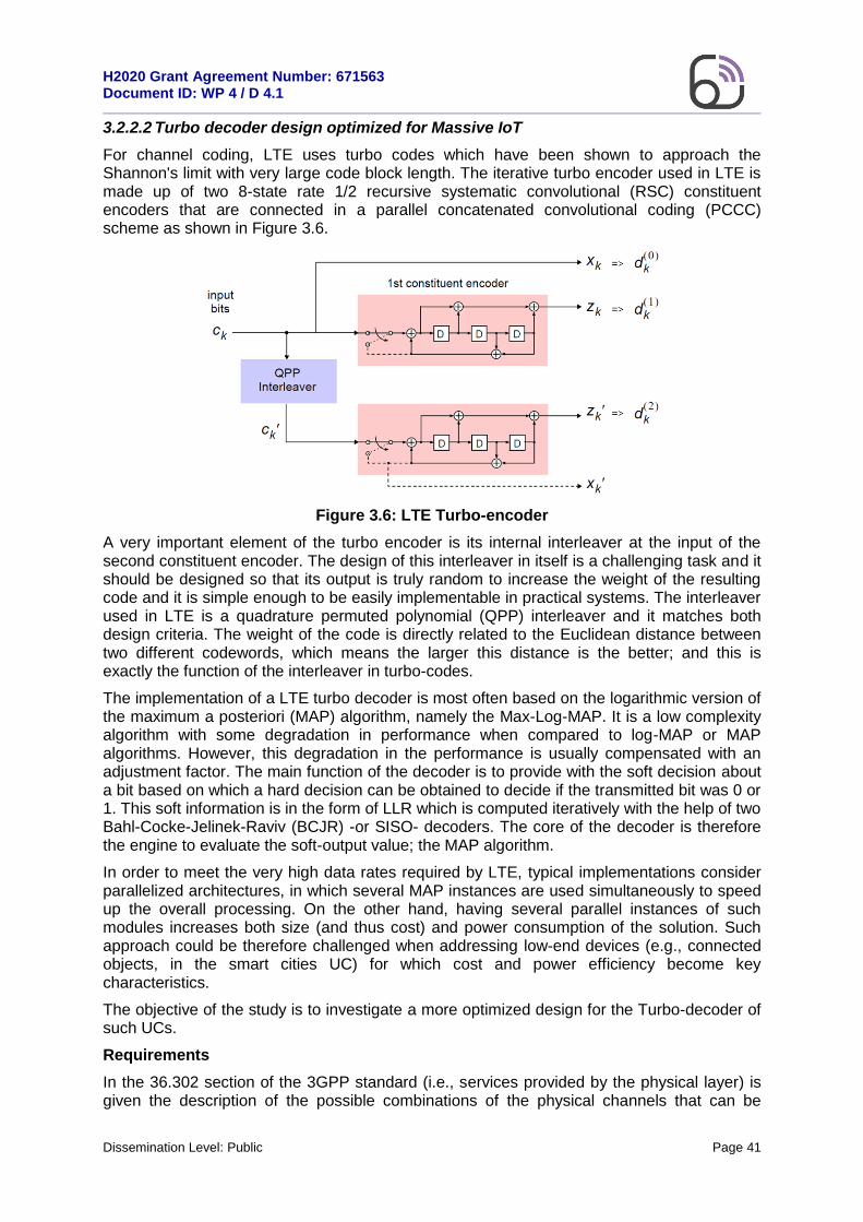
H2020 Grant Agreement Number: 671563 Document ID: WP 4 / D 4.1
Dissemination Level: Public Page 41
3.2.2.2 Turbo decoder design optimized for Massive IoT
For channel coding, LTE uses turbo codes which have been shown to approach the Shannon's limit with very large code block length. The iterative turbo encoder used in LTE is made up of two 8-state rate 1/2 recursive systematic convolutional (RSC) constituent encoders that are connected in a parallel concatenated convolutional coding (PCCC) scheme as shown in Figure 3.6.
Figure 3.6: LTE Turbo-encoder
A very important element of the turbo encoder is its internal interleaver at the input of the second constituent encoder. The design of this interleaver in itself is a challenging task and it should be designed so that its output is truly random to increase the weight of the resulting code and it is simple enough to be easily implementable in practical systems. The interleaver used in LTE is a quadrature permuted polynomial (QPP) interleaver and it matches both design criteria. The weight of the code is directly related to the Euclidean distance between two different codewords, which means the larger this distance is the better; and this is exactly the function of the interleaver in turbo-codes.
The implementation of a LTE turbo decoder is most often based on the logarithmic version of the maximum a posteriori (MAP) algorithm, namely the Max-Log-MAP. It is a low complexity algorithm with some degradation in performance when compared to log-MAP or MAP algorithms. However, this degradation in the performance is usually compensated with an adjustment factor. The main function of the decoder is to provide with the soft decision about a bit based on which a hard decision can be obtained to decide if the transmitted bit was 0 or 1. This soft information is in the form of LLR which is computed iteratively with the help of two Bahl-Cocke-Jelinek-Raviv (BCJR) -or SISO- decoders. The core of the decoder is therefore the engine to evaluate the soft-output value; the MAP algorithm.
In order to meet the very high data rates required by LTE, typical implementations consider parallelized architectures, in which several MAP instances are used simultaneously to speed up the overall processing. On the other hand, having several parallel instances of such modules increases both size (and thus cost) and power consumption of the solution. Such approach could be therefore challenged when addressing low-end devices (e.g., connected objects, in the smart cities UC) for which cost and power efficiency become key characteristics.
The objective of the study is to investigate a more optimized design for the Turbo-decoder of such UCs.
Requirements
In the 36.302 section of the 3GPP standard (i.e., services provided by the physical layer) is given the description of the possible combinations of the physical channels that can be

H2020 Grant Agreement Number: 671563 Document ID: WP 4 / D 4.1
Dissemination Level: Public Page 42
received in the same subframe on the downlink by one UE. These physical channels are transmitted separately via a distinct transport block (TB). For cases that do not fall within the multicast-broadcast single-frequency network (MBSFN), the supported combination is, {A + B + C + (D or E or G or I) + (F or H or J) + M} where A, B, C, D, E, F, G, H, I, J, K, L, M are described in the Figure 3.7. This means that there can be three (or four if Physical Downlink Shared Channel (PDSCH) communications are with 2 layers) TBs, which need to be decoded by the turbo decoder in one subframe such that it applies:
SI-RNTI and P-RNTI and ((RA-RNTI or TC-RNTI) or (C-RNTI or SPS-RNTI)) where:
RNTI is the radio network temporary identifier
SI-RNTI is the system information RNTI
P-RNTI is the paging RNTI
RA-RNTI is the random access RNTI
TC-RNTI is the temporary cell RNTI
SPS-RNTI is the semi-persistent scheduling RNTI
Figure 3.7: Downlink reception types (from the 3GPP 36.302 specification).
SI-RNTI is context 0, P-RNTI is context 1 and RA-RNTI/C-RNTI/TC-RNTI/SPS-RNTI are context 2. Context 3 is used for the second layer corresponding to C-RNTI in dual layer transmission. For category 0 we quote from the 36.306 3GPP specification “Within one transmission time interval (TTI), a UE indicating category 0 shall be able to receive up to

H2020 Grant Agreement Number: 671563 Document ID: WP 4 / D 4.1
Dissemination Level: Public Page 43
1000 bits for a transport block associated with C-RNTI/Semi-Persistent Scheduling C-RNTI/P-RNTI/SI-RNTI/RA-RNTI and up to 2216 bits for another transport block associated with P-RNTI/SI-RNTI/RA-RNTI”. Furthermore, at the same specification it is mentioned that the maximum number of layers in category 0 is one and the maximum code block (CB) size is 2216 bits. This is smaller than maximum CB size limit (6144), therefore, in category 0, CB = TB in contrast to category 4 where there can be up to 28 CBs in 4 TBs.
With these requirements for category 0 it is required to decode maximum of 3 CBs in a subframe each of size up to 2216 bits. Defining this requirement shall help in the optimized design of the turbo decoder. Similar analysis could be made for the category M. In category M there shall be no simultaneous reception, i.e., just one CB to be decoded, which can be up to 1000 bits.
Requirements
Finally, the Table 3.5 that follows describes which WP4 requirements apply to the described concept.
Table 3.5: Relevant WP4 requirements for the described specifications and concept.
ID Requirement Description
COMP-1 Processing performance Processing performance will be evaluated thanks to simulation.
IMPL-5 Low processing footprint Capacity to minimize the processing load in energy or computationally constrained baseband systems.
ARCH-7 Cost reduction The ability to reduce the costs related with the digital HW and those related
with the intrinsics of its operation.

H2020 Grant Agreement Number: 671563 Document ID: WP 4 / D 4.1
Dissemination Level: Public Page 44
3.2.3 Multiprocessor baseband architectures for 5G network elements
Baseband processing is one of the most computationally intensive component of current network element products i.e. base stations. Sometimes the term baseband processing is used to describe all the processing required to implement signalling layers L1, L2 and L3. The scope of this study is to provide a baseband processor architecture for physical layer (L1) processing including also digital radio front-end functionalities.
The baseband processors of 5G network elements will require very high computational capacity and flexibility. The computational capacity increase is caused by high bandwidth and bit rate requirements and also by new algorithms needed to achieve increase in the network capacity. Flexibility is needed in the baseband processor for various reasons. 5G base stations should handle a variable number of connections with dynamically changing throughput requirements. Multiple radio access technologies will be used concurrently and the computational load for processing different RAT’s will vary dynamically. There would also be dynamic variation in the uplink and downlink traffic. Scalability of the baseband processor architecture is needed to be suitable for different kind of network element products.
The energy efficiency of the baseband processor can be optimised with an architecture that is based on fixed algorithm-specific hardware blocks. The high flexibility requirement makes the cost of this approach intolerable. A typical approach is to use general purpose processors and/or digital signal processors to achieve adequate flexibility in the baseband architecture. The required energy efficiency for the baseband processor is then achieved by using a set of hardware blocks for implementing the most critical functionalities.
The goal of this study is to utilise the REPLICA chip5 multi-processor framework for the baseband processor architecture. The current REPLICA architecture is targeted for general purpose processing, thus optimisation for baseband processing is needed. Existing air interfaces will be supported by 5G network elements, thus the LTE physical layer functionalities will be used as the baseline for the architecture optimisation. Proposals of new air interfaces for 5G with corresponding transceiver algorithms will be taken into account in the second phase of the architecture optimisation.
REPLICA is a chip multiprocessor (CMP) framework aimed at addressing performance, flexibility and programmability problems of current CMPs offerings. These problems are caused by insufficient scaling of latency tolerance, highly expensive/inefficient synchronization, bounded co-exploitation of instruction-level and thread-level parallelism, error-prone and complex asynchronous computational model, and (weak) sequential memory consistency. The key techniques to achieve these goals are latency hiding with multithreading (other threads are executed while a thread refers to the shared memory), cost-efficient synchronization with a wave-based hardware mechanism and improved instruction-level parallelism (ILP) via chaining of operations on the execution pipeline. Simple parallel programmability is achieved by using these architectural techniques to realize a strong synchronous model of computation with strict memory consistency.
A REPLICA CMP consists of P replicated tiles composed of a Multi-Bunched/Threaded Architecture Chaining (MBTAC) processor, a shared memory module, an instruction memory module, and a local memory module (see Figure 3.8). The processors and shared memory modules are connected together via a high-bandwidth REPLICA network that can also be dedicated to signal propagation.
MBTAC is a dual-mode multithreaded very long instruction word (VLIW) processor. The VLIW scheme is used instead of dynamic out-of-order superscalar execution due to determinism and synchronization reasons. Each MBTAC processor consists of A arithmetic logical units (ALU), M shared memory units (MU), L local memory units (LMU), and sequencers for both high-throughput and minimum latency conventions. A processor uses
5 http://www.vtt.fi/sites/replica/en/replica-architecture
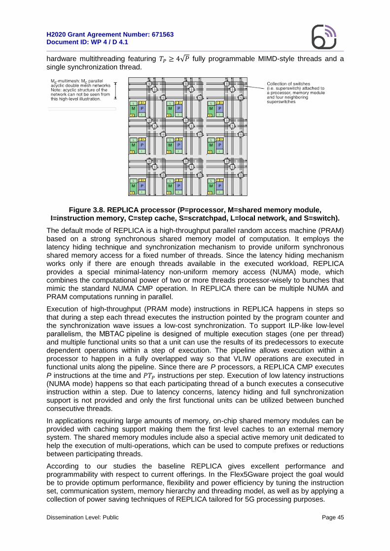
H2020 Grant Agreement Number: 671563 Document ID: WP 4 / D 4.1
Dissemination Level: Public Page 45
hardware multithreading featuring 𝑇𝑃 ≥ 4√𝑃 fully programmable MIMD-style threads and a single synchronization thread.
Figure 3.8. REPLICA processor (P=processor, M=shared memory module, I=instruction memory, C=step cache, S=scratchpad, L=local network, and S=switch).
The default mode of REPLICA is a high-throughput parallel random access machine (PRAM) based on a strong synchronous shared memory model of computation. It employs the latency hiding technique and synchronization mechanism to provide uniform synchronous shared memory access for a fixed number of threads. Since the latency hiding mechanism works only if there are enough threads available in the executed workload, REPLICA provides a special minimal-latency non-uniform memory access (NUMA) mode, which combines the computational power of two or more threads processor-wisely to bunches that mimic the standard NUMA CMP operation. In REPLICA there can be multiple NUMA and PRAM computations running in parallel.
Execution of high-throughput (PRAM mode) instructions in REPLICA happens in steps so that during a step each thread executes the instruction pointed by the program counter and the synchronization wave issues a low-cost synchronization. To support ILP-like low-level parallelism, the MBTAC pipeline is designed of multiple execution stages (one per thread) and multiple functional units so that a unit can use the results of its predecessors to execute dependent operations within a step of execution. The pipeline allows execution within a processor to happen in a fully overlapped way so that VLIW operations are executed in functional units along the pipeline. Since there are P processors, a REPLICA CMP executes
P instructions at the time and 𝑃𝑇𝑃 instructions per step. Execution of low latency instructions (NUMA mode) happens so that each participating thread of a bunch executes a consecutive instruction within a step. Due to latency concerns, latency hiding and full synchronization support is not provided and only the first functional units can be utilized between bunched consecutive threads.
In applications requiring large amounts of memory, on-chip shared memory modules can be provided with caching support making them the first level caches to an external memory system. The shared memory modules include also a special active memory unit dedicated to help the execution of multi-operations, which can be used to compute prefixes or reductions between participating threads.
According to our studies the baseline REPLICA gives excellent performance and programmability with respect to current offerings. In the Flex5Gware project the goal would be to provide optimum performance, flexibility and power efficiency by tuning the instruction set, communication system, memory hierarchy and threading model, as well as by applying a collection of power saving techniques of REPLICA tailored for 5G processing purposes.
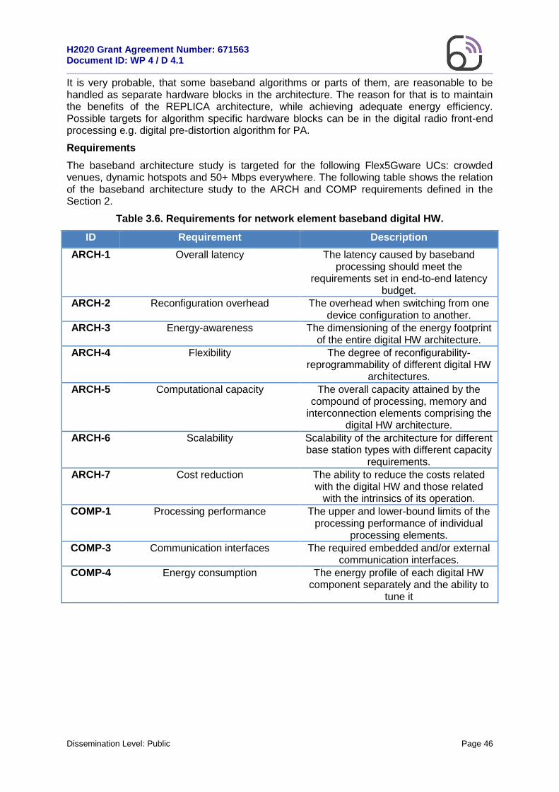
H2020 Grant Agreement Number: 671563 Document ID: WP 4 / D 4.1
Dissemination Level: Public Page 46
It is very probable, that some baseband algorithms or parts of them, are reasonable to be handled as separate hardware blocks in the architecture. The reason for that is to maintain the benefits of the REPLICA architecture, while achieving adequate energy efficiency. Possible targets for algorithm specific hardware blocks can be in the digital radio front-end processing e.g. digital pre-distortion algorithm for PA.
Requirements
The baseband architecture study is targeted for the following Flex5Gware UCs: crowded venues, dynamic hotspots and 50+ Mbps everywhere. The following table shows the relation of the baseband architecture study to the ARCH and COMP requirements defined in the Section 2.
Table 3.6. Requirements for network element baseband digital HW.
ID Requirement Description
ARCH-1 Overall latency The latency caused by baseband processing should meet the
requirements set in end-to-end latency budget.
ARCH-2 Reconfiguration overhead The overhead when switching from one device configuration to another.
ARCH-3 Energy-awareness The dimensioning of the energy footprint of the entire digital HW architecture.
ARCH-4 Flexibility The degree of reconfigurability-reprogrammability of different digital HW
architectures.
ARCH-5 Computational capacity The overall capacity attained by the compound of processing, memory and
interconnection elements comprising the digital HW architecture.
ARCH-6 Scalability Scalability of the architecture for different base station types with different capacity
requirements.
ARCH-7 Cost reduction The ability to reduce the costs related with the digital HW and those related
with the intrinsics of its operation.
COMP-1 Processing performance The upper and lower-bound limits of the processing performance of individual
processing elements.
COMP-3 Communication interfaces The required embedded and/or external communication interfaces.
COMP-4 Energy consumption The energy profile of each digital HW component separately and the ability to
tune it

H2020 Grant Agreement Number: 671563 Document ID: WP 4 / D 4.1
Dissemination Level: Public Page 47
3.3 Digital HW architectures optimising flexibility
3.3.1 Flexible HW-SW partitioning solutions for 5G
3.3.1.1 Architecture for supporting MAC/PHY cross-layer reconfigurations
In this Section we provide the requirements and the general concepts for the design of a terminal architecture devised to permit control and orchestration of elementary hardware primitives (module/de-module, scramble, interleave, schedule, etc.) by means of a suitable language formalization able to describe a complete MAC/PHY stack. The idea is moving from the traditional approach of “one-size-fits-all” protocol stack to an innovative paradigm of opportunistically on-the-fly configuration of context-specific stacks.
The work does not start from scratch, because in the FP7 European project FLAVIA6 we already showed how to decouple the MAC protocol logic (described in an abstract form via eXtended finite state machines XFSMs) from the wireless device design, implementing the radio primitives as well as an XFSM execution engine called wireless MAC processor (WMP). In the WMP architecture, the radio primitives correspond to the pre-implemented actions available on the hardware and on the pre-implemented events triggered by specific hardware signals. In order to extend this concept to the overall MAC/PHY stack, we plan to work both on the programming language, that now has to also define the chain of operations performing the TX/RX operations, and on the hardware architecture, that has to decouple the current TX/RX primitives into more elementary configurable blocks.
Figure 3.9: The overall envisioned WMP architecture
Figure shows the envisioned architecture for extending the WMP concept. The Radio engine is the core of the architecture, because it is the component responsible of controlling the hardware functionalities by running an abstract Radio Program. While in the original WMP architecture the hardware functionalities were mainly embedded into pre-defined transmission modes with a fixed bandwidth, we are now considering a decomposition of the transmitter and receiver chain in order to support spectrum agility, antenna configurations and cross-layer MAC/PHY interactions (e.g. selecting a different transmission mode for each destination node).
Requirements
The proposed terminal architecture has to support MAC/PHY flexibility, in terms of: i) capability of running completely different MAC protocols, from time division multiple access
6 http://www.ict-flavia.eu/
Wireless(PHY+MAC)SW/HWPla orm
RADIOENGINE
legend
DATA
CTRL
Registers/Memory
Interrupts
Opera ons
PHYTX/RXModules
Micro-instruc onMemory
RadioProgram(i)RadioProgram(i)RadioProgram(i)
TX/RXDATA
QUEU
ES
RADIOPROGRAMMANAGER
010101010101010101010011
Upper-levelservices
inject(i)run(i)
ANALOG/ANTENNA
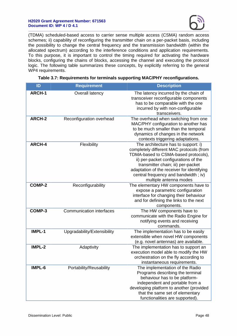
H2020 Grant Agreement Number: 671563 Document ID: WP 4 / D 4.1
Dissemination Level: Public Page 48
(TDMA) scheduled-based access to carrier sense multiple access (CSMA) random access schemes; ii) capability of reconfiguring the transmitter chain on a per-packet basis, including the possibility to change the central frequency and the transmission bandwidth (within the allocated spectrum) according to the interference conditions and application requirements. To this purpose, it is important to control the timing required for activating the hardware blocks, configuring the chains of blocks, accessing the channel and executing the protocol logic. The following table summarizes these concepts, by explicitly referring to the general WP4 requirements.
Table 3.7: Requirements for terminals supporting MAC/PHY reconfigurations.
ID Requirement Description
ARCH-1 Overall latency The latency incurred by the chain of transceiver reconfigurable components
has to be comparable with the one incurred by with non-configurable
transceivers.
ARCH-2 Reconfiguration overhead The overhead when switching from one MAC/PHY configuration to another has to be much smaller than the temporal dynamics of changes in the network
contexts triggering adaptations.
ARCH-4 Flexibility The architecture has to support: i) completely different MAC protocols (from TDMA-based to CSMA-based protocols),
ii) per-packet configurations of the transmitter chain; iii) per-packet
adaptation of the receiver for identifying central frequency and bandwidth ; iv)
multiple antenna modes
COMP-2 Reconfigurability The elementary HW components have to expose a parametric configuration
interface for changing their behaviour and for defining the links to the next
components.
COMP-3 Communication interfaces The HW components have to communicate with the Radio Engine for
notifying events and receiving commands.
IMPL-1 Upgradability/Extensibility The implementation has to be easily extensible when novel HW components
(e.g. novel antennas) are available.
IMPL-2 Adaptivity The implementation has to support an execution model able to modify the HW
orchestration on the fly according to instantaneous requirements.
IMPL-6 Portability/Reusability The implementation of the Radio Programs describing the terminal
behaviour has to be platform-independent and portable from a
developing platform to another (provided that the same set of elementary functionalities are supported).

H2020 Grant Agreement Number: 671563 Document ID: WP 4 / D 4.1
Dissemination Level: Public Page 49
Developing Platform
For prototyping the proposed terminal architecture, we will work on the WARP v3 research platform7 that is a FPGA-based software-defined-radio platform. As shown in Figure 3.10, the global architecture of this research board can be divided in two parts: an RF hardware interface, given by the transceiver (MAX2829), analogue-to-digital converter (ADC)/digital-to-analogue converter (DAC) chip (AD9963) and hardware for clocking (AD9512), and an FPGA programmable part (Virtex-6 Xilinx).
For this board, some implementations of MAC/PHY stacks are already available. In particular, an 802.11g MAC/PHY stack has been developed under the name of 802.11 reference design. The architecture is based on two MicroBlaze processors and some dedicated intellectual property (IP) cores developed within the FPGA board, as shown in Figure 1.11.
Figure 3.10: Architecture of the WARP research board.
Figure 1.11: The 802.11 MAC/PHY reference design.
As detailed in the WARP project site8, the architecture includes:
two MicroBlaze CPUs, called CPU High and CPU Low;
a MAC distributed coordination function (DCF) core;
two PHY cores, one for the transmission TX and the other for the receiving RX
Hardware Support cores.
7 https://warpproject.org/trac 8 https://warpproject.org/trac/wiki/802.11/Architecture
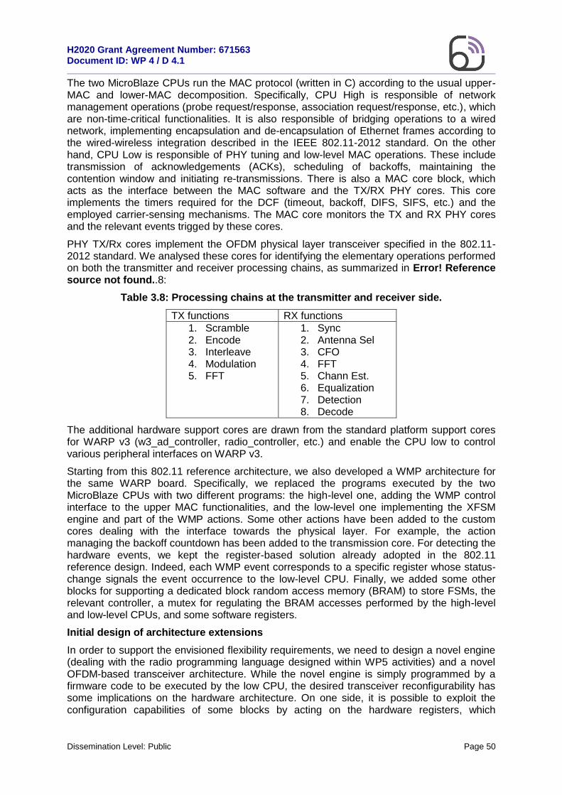
H2020 Grant Agreement Number: 671563 Document ID: WP 4 / D 4.1
Dissemination Level: Public Page 50
The two MicroBlaze CPUs run the MAC protocol (written in C) according to the usual upper-MAC and lower-MAC decomposition. Specifically, CPU High is responsible of network management operations (probe request/response, association request/response, etc.), which are non-time-critical functionalities. It is also responsible of bridging operations to a wired network, implementing encapsulation and de-encapsulation of Ethernet frames according to the wired-wireless integration described in the IEEE 802.11-2012 standard. On the other hand, CPU Low is responsible of PHY tuning and low-level MAC operations. These include transmission of acknowledgements (ACKs), scheduling of backoffs, maintaining the contention window and initiating re-transmissions. There is also a MAC core block, which acts as the interface between the MAC software and the TX/RX PHY cores. This core implements the timers required for the DCF (timeout, backoff, DIFS, SIFS, etc.) and the employed carrier-sensing mechanisms. The MAC core monitors the TX and RX PHY cores and the relevant events trigged by these cores.
PHY TX/Rx cores implement the OFDM physical layer transceiver specified in the 802.11-2012 standard. We analysed these cores for identifying the elementary operations performed on both the transmitter and receiver processing chains, as summarized in Error! Reference source not found..8:
Table 3.8: Processing chains at the transmitter and receiver side.
TX functions RX functions
1. Scramble 2. Encode 3. Interleave 4. Modulation 5. FFT
1. Sync 2. Antenna Sel 3. CFO 4. FFT 5. Chann Est. 6. Equalization 7. Detection 8. Decode
The additional hardware support cores are drawn from the standard platform support cores for WARP v3 (w3_ad_controller, radio_controller, etc.) and enable the CPU low to control various peripheral interfaces on WARP v3.
Starting from this 802.11 reference architecture, we also developed a WMP architecture for the same WARP board. Specifically, we replaced the programs executed by the two MicroBlaze CPUs with two different programs: the high-level one, adding the WMP control interface to the upper MAC functionalities, and the low-level one implementing the XFSM engine and part of the WMP actions. Some other actions have been added to the custom cores dealing with the interface towards the physical layer. For example, the action managing the backoff countdown has been added to the transmission core. For detecting the hardware events, we kept the register-based solution already adopted in the 802.11 reference design. Indeed, each WMP event corresponds to a specific register whose status-change signals the event occurrence to the low-level CPU. Finally, we added some other blocks for supporting a dedicated block random access memory (BRAM) to store FSMs, the relevant controller, a mutex for regulating the BRAM accesses performed by the high-level and low-level CPUs, and some software registers.
Initial design of architecture extensions
In order to support the envisioned flexibility requirements, we need to design a novel engine (dealing with the radio programming language designed within WP5 activities) and a novel OFDM-based transceiver architecture. While the novel engine is simply programmed by a firmware code to be executed by the low CPU, the desired transceiver reconfigurability has some implications on the hardware architecture. On one side, it is possible to exploit the configuration capabilities of some blocks by acting on the hardware registers, which
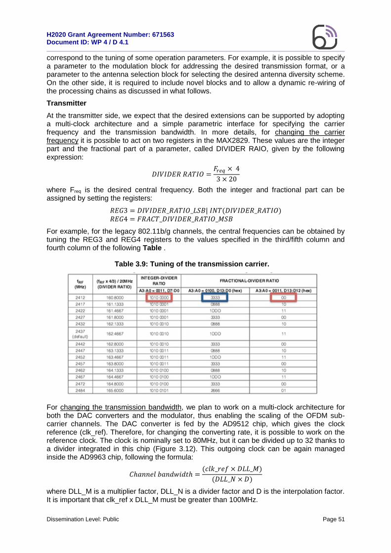
H2020 Grant Agreement Number: 671563 Document ID: WP 4 / D 4.1
Dissemination Level: Public Page 51
correspond to the tuning of some operation parameters. For example, it is possible to specify a parameter to the modulation block for addressing the desired transmission format, or a parameter to the antenna selection block for selecting the desired antenna diversity scheme. On the other side, it is required to include novel blocks and to allow a dynamic re-wiring of the processing chains as discussed in what follows.
Transmitter
At the transmitter side, we expect that the desired extensions can be supported by adopting a multi-clock architecture and a simple parametric interface for specifying the carrier frequency and the transmission bandwidth. In more details, for changing the carrier frequency it is possible to act on two registers in the MAX2829. These values are the integer part and the fractional part of a parameter, called DIVIDER RAIO, given by the following expression:
𝐷𝐼𝑉𝐼𝐷𝐸𝑅 𝑅𝐴𝑇𝐼𝑂 =𝐹𝑟𝑒𝑞 × 4
3 × 20
where Freq is the desired central frequency. Both the integer and fractional part can be assigned by setting the registers:
𝑅𝐸𝐺3 = 𝐷𝐼𝑉𝐼𝐷𝐸𝑅_𝑅𝐴𝑇𝐼𝑂_𝐿𝑆𝐵| 𝐼𝑁𝑇(𝐷𝐼𝑉𝐼𝐷𝐸𝑅_𝑅𝐴𝑇𝐼𝑂) 𝑅𝐸𝐺4 = 𝐹𝑅𝐴𝐶𝑇_𝐷𝐼𝑉𝐼𝐷𝐸𝑅_𝑅𝐴𝑇𝐼𝑂_𝑀𝑆𝐵
For example, for the legacy 802.11b/g channels, the central frequencies can be obtained by tuning the REG3 and REG4 registers to the values specified in the third/fifth column and fourth column of the following Table .
Table 3.9: Tuning of the transmission carrier.
For changing the transmission bandwidth, we plan to work on a multi-clock architecture for both the DAC converters and the modulator, thus enabling the scaling of the OFDM sub-carrier channels. The DAC converter is fed by the AD9512 chip, which gives the clock reference (clk_ref). Therefore, for changing the converting rate, it is possible to work on the reference clock. The clock is nominally set to 80MHz, but it can be divided up to 32 thanks to a divider integrated in this chip (Figure 3.12). This outgoing clock can be again managed inside the AD9963 chip, following the formula:
𝐶ℎ𝑎𝑛𝑛𝑒𝑙 𝑏𝑎𝑛𝑑𝑤𝑖𝑑𝑡ℎ =(𝑐𝑙𝑘_𝑟𝑒𝑓 × 𝐷𝐿𝐿_𝑀)
(𝐷𝐿𝐿_𝑁 × 𝐷)
where DLL_M is a multiplier factor, DLL_N is a divider factor and D is the interpolation factor. It is important that clk_ref x DLL_M must be greater than 100MHz.
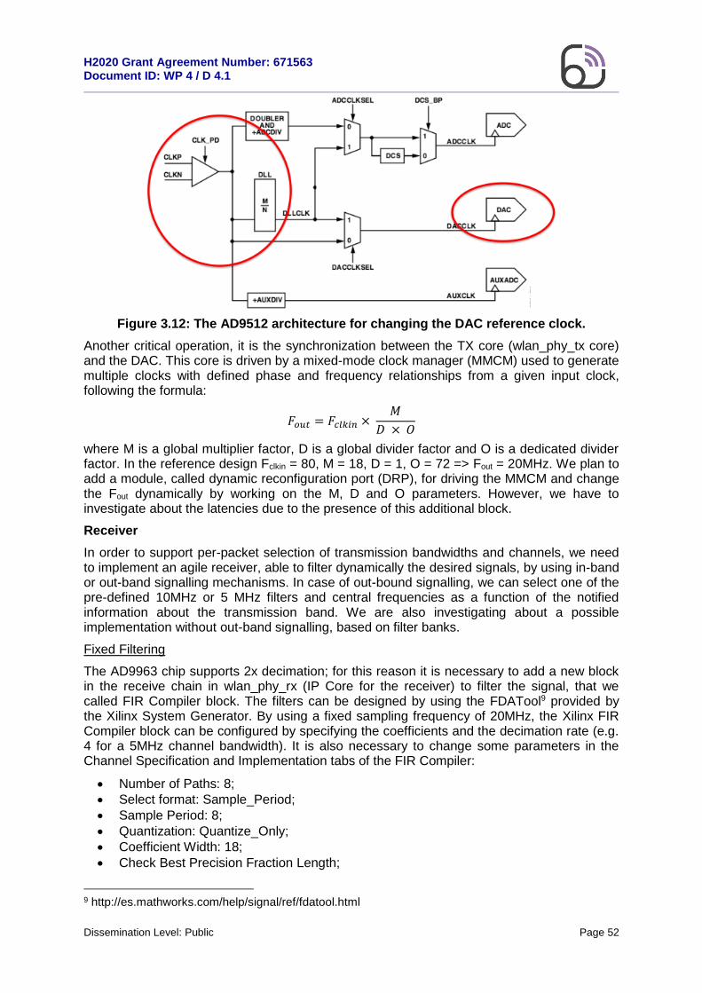
H2020 Grant Agreement Number: 671563 Document ID: WP 4 / D 4.1
Dissemination Level: Public Page 52
Figure 3.12: The AD9512 architecture for changing the DAC reference clock.
Another critical operation, it is the synchronization between the TX core (wlan_phy_tx core) and the DAC. This core is driven by a mixed-mode clock manager (MMCM) used to generate multiple clocks with defined phase and frequency relationships from a given input clock, following the formula:
𝐹𝑜𝑢𝑡 = 𝐹𝑐𝑙𝑘𝑖𝑛 × 𝑀
𝐷 × 𝑂
where M is a global multiplier factor, D is a global divider factor and O is a dedicated divider factor. In the reference design Fclkin = 80, M = 18, D = 1, O = 72 => Fout = 20MHz. We plan to add a module, called dynamic reconfiguration port (DRP), for driving the MMCM and change the Fout dynamically by working on the M, D and O parameters. However, we have to investigate about the latencies due to the presence of this additional block.
Receiver
In order to support per-packet selection of transmission bandwidths and channels, we need to implement an agile receiver, able to filter dynamically the desired signals, by using in-band or out-band signalling mechanisms. In case of out-bound signalling, we can select one of the pre-defined 10MHz or 5 MHz filters and central frequencies as a function of the notified information about the transmission band. We are also investigating about a possible implementation without out-band signalling, based on filter banks.
Fixed Filtering
The AD9963 chip supports 2x decimation; for this reason it is necessary to add a new block in the receive chain in wlan_phy_rx (IP Core for the receiver) to filter the signal, that we called FIR Compiler block. The filters can be designed by using the FDATool9 provided by the Xilinx System Generator. By using a fixed sampling frequency of 20MHz, the Xilinx FIR Compiler block can be configured by specifying the coefficients and the decimation rate (e.g. 4 for a 5MHz channel bandwidth). It is also necessary to change some parameters in the Channel Specification and Implementation tabs of the FIR Compiler:
Number of Paths: 8;
Select format: Sample_Period;
Sample Period: 8;
Quantization: Quantize_Only;
Coefficient Width: 18;
Check Best Precision Fraction Length;
9 http://es.mathworks.com/help/signal/ref/fdatool.html
H2020 Grant Agreement Number: 671563 Document ID: WP 4 / D 4.1
Dissemination Level: Public Page 53
Output Rounding Mode: Truncate_LSBs;
Output Width: 16.
Then, the input ports of the new block are connected to the appropriate signals that come from the ADC in the AD9963. Finally, it is necessary to generate the VHDL code and integrate this in the Xilinx XPS project.
Multirate Filters
For supporting an agile receiver in which the configuration of central frequency and bandwidth is not given by an out-band channel, we are considering a novel receiver architecture based on multirate filters. We are planning to study, first in MATLAB and then over the WARPv3 SDR platform, a digital orthogonal filterbank system which will be used for:
- decomposition of the received signal in narrow subbands: this step will draw from well-known low latency multirate decomposition techniques which can be implemented as FBMC systems;
- received signal bandwidth and centre frequency detection: this step will be implemented, at first, as an incoherent per-subband energy detector, and will produce a rough estimate of the signal bandwidth and centre frequency;
- synthesis of the downconverted and eventually downsampled received signal: this step will be implemented composing the selected subbands in order to synthesize the received signal to an equivalent downconverted (i.e. having a centre frequency approximately equal to zero), and eventually downsampled/resampled at a frequency compatible with the subsequent fine frequency synchronization.
The complete system will enable the agile receiver to dynamically detect the bandwidth and centre frequency of incoming transmissions, without previous negotiation with the transmitters.
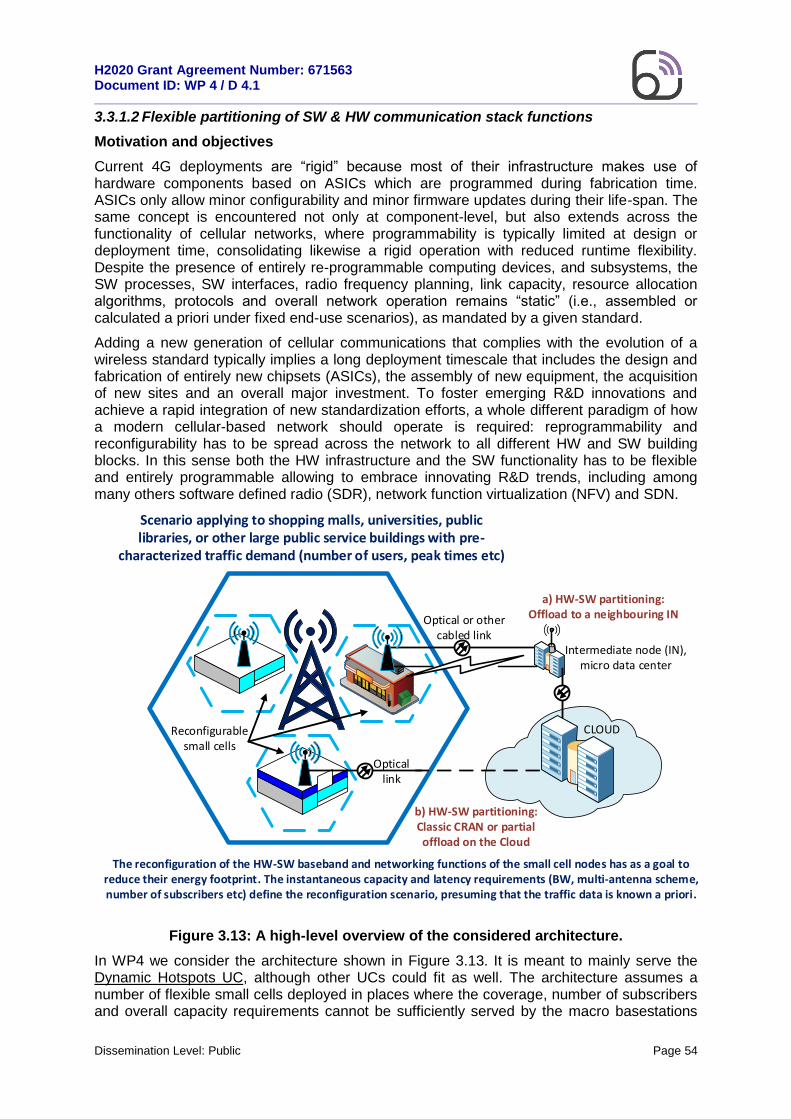
H2020 Grant Agreement Number: 671563 Document ID: WP 4 / D 4.1
Dissemination Level: Public Page 54
3.3.1.2 Flexible partitioning of SW & HW communication stack functions
Motivation and objectives
Current 4G deployments are “rigid” because most of their infrastructure makes use of hardware components based on ASICs which are programmed during fabrication time. ASICs only allow minor configurability and minor firmware updates during their life-span. The same concept is encountered not only at component-level, but also extends across the functionality of cellular networks, where programmability is typically limited at design or deployment time, consolidating likewise a rigid operation with reduced runtime flexibility. Despite the presence of entirely re-programmable computing devices, and subsystems, the SW processes, SW interfaces, radio frequency planning, link capacity, resource allocation algorithms, protocols and overall network operation remains “static” (i.e., assembled or calculated a priori under fixed end-use scenarios), as mandated by a given standard.
Adding a new generation of cellular communications that complies with the evolution of a wireless standard typically implies a long deployment timescale that includes the design and fabrication of entirely new chipsets (ASICs), the assembly of new equipment, the acquisition of new sites and an overall major investment. To foster emerging R&D innovations and achieve a rapid integration of new standardization efforts, a whole different paradigm of how a modern cellular-based network should operate is required: reprogrammability and reconfigurability has to be spread across the network to all different HW and SW building blocks. In this sense both the HW infrastructure and the SW functionality has to be flexible and entirely programmable allowing to embrace innovating R&D trends, including among many others software defined radio (SDR), network function virtualization (NFV) and SDN.
Optical link
Optical or other cabled link
CLOUD
Intermediate node (IN),micro data center
Scenario applying to shopping malls, universities, public libraries, or other large public service buildings with pre-
characterized traffic demand (number of users, peak times etc)
Reconfigurablesmall cells
b) HW-SW partitioning: Classic CRAN or partial offload on the Cloud
a) HW-SW partitioning:Offload to a neighbouring IN
The reconfiguration of the HW-SW baseband and networking functions of the small cell nodes has as a goal to reduce their energy footprint. The instantaneous capacity and latency requirements (BW, multi-antenna scheme, number of subscribers etc) define the reconfiguration scenario, presuming that the traffic data is known a priori.
Figure 3.13: A high-level overview of the considered architecture.
In WP4 we consider the architecture shown in Figure 3.13. It is meant to mainly serve the Dynamic Hotspots UC, although other UCs could fit as well. The architecture assumes a number of flexible small cells deployed in places where the coverage, number of subscribers and overall capacity requirements cannot be sufficiently served by the macro basestations

H2020 Grant Agreement Number: 671563 Document ID: WP 4 / D 4.1
Dissemination Level: Public Page 55
(BSs). Such places include, among others, shopping malls, university campuses, large venues, central train stations, public libraries or other large public-service buildings. The goal of this development is to provide a flexible 5G networking architecture where the HW-accelerated (HWA) and SW communication stack functions of small cells (dynamic hotspots) can be reconfigured in order to serve different KPIs; this would be made feasible by partitioning and distributing such functions across different nodes of the network and/or by tuning certain baseband parameters. The network reconfiguration could be realized either by connecting the small cells with neighbouring intermediate nodes (INs) e.g., other small cells or local micro data centers according to mobile edge computing (MEC)10 paradigms, or directly with Cloud computing solutions. In the absence of a fully defined 5G air interface, the 4G LTE will be considered as a basis. The reconfiguration would be applied at two levels as detailed in the following:
i. NETCFG: Switch from a given network configuration to another one that features a different partitioning of its underlying SW and HWA functions.
ii. WCP: Tuning specific wireless communication parameters or a functional set of L1 blocks. This, for instance, could encompass signal bandwidth scaling, selection of a multi or single antenna operating mode, selection of a suitable modulation and coding scheme, waveform modification (e.g., from 4G to 5G) or waveform aggregation (to exploit unused spectrum) and adaptive transmission power.
In the context of this project, the reconfiguration of NETCFGs or WCPs will not be dynamic, but it would rather be based on offline switching between given configurations. Nevertheless, the network-wide implications of the dynamic run-time reconfiguration will be studied, in order to add this feature in a future development roadmap.
As far as the dynamic hotspot UC is concerned, the transitions from one NETCFG to another would be made to guarantee the NRG KPI at eNB level. Nevertheless the versatility of the proposed solution could also serve other KPIs, such as the UDR, LAT, BW, NoU, MDV, RES, CST and of course the FVR.
This development is timely considering that the small cell forum (SCF) has recently promoted11 the partitioning of the eNB protocol stack, either at stack-level or algorithm-level (e.g., MAC-PHY, RLC, PDCP). The goal of this split is to maintain the benefits of CRAN, while relaxing at the same time the stringent latency and bandwidth requirements of CPRI fronthaul (FH), which typically is an ideal transport connection (e.g., dark-fiber); hence this would allow FH links to be transported over the packet-switched networks, which are conventionally used to support small cell deployments (e.g., nation-wide, low-cost IP networks).
An illustrative example that could find a practical and realistic use in the context of the dynamic hotspot UC is the following: a mobile operator wants to benefit from the fact that the data-traffic decreases during lunch time, between 12:30 pm and 2:00 pm. We assume that the traffic volume patterns and tendencies are known a priori. Hence at this time slot, the operator scales the signal bandwidth of the small cells from 20 to 5 MHz and also switches from one NETCFG to another, in order to achieve energy savings at baseband processing, RF transceiver and PA level.
Requirements
The relation of this contribution with the ARCH, COMP and IMPL requirements defined in Section 2 is detailed in Table 3.10.
10 http://www.etsi.org/technologies-clusters/technologies/mobile-edge-computing 11 “Virtualization for small cells: Overview”: http://www.scf.io/en/documents/106__Virtualization_for_small_cells_Overview.php

H2020 Grant Agreement Number: 671563 Document ID: WP 4 / D 4.1
Dissemination Level: Public Page 56
Table 3.10: WP4 requirements related to the flexible partitioning of HWA/SW communication stack functions.
ID Requirement Comment
ARCH-1 Overall latency The compound latency of each NETCFG needs to be considered, in
order to determine which one satisfies the instantaneous operating
requirements.
ARCH-2 Reconfiguration overhead Changing from one NETCFG to another will add top-up latencies. These will be studied for future inclusion of dynamic
reconfiguration features.
ARCH-3 Energy-awareness Each NETCFG and WCP setup will present a different energy foot-print.
This can be exploited to save energy.
ARCH-4 Flexibility Supporting multiple NETCFGs requires the availability and proper configuration of various interfacing elements (both at
HW and SW levels).
ARCH-6 Scalability The computational, memory and interfacing requirements when selecting different WCP must be contemplated.
ARCH-8 Availability As part of the inclusion of dynamic reconfiguration features in the future,
mechanisms will be analysed so as the network reconfiguration would not disrupt the user services. Similarly
recovery mechanisms will be analysed in case the newly adopted configuration
fails or is not able to meet the instantaneous operating
requirements12.
COMP-1 Processing performance Each baseband/networking function needs to be hosted in a processing component providing an adequate
computational capacity according to the instantaneous operating requirements.
COMP-2 Reconfigurability The modification of the considered WCP requires the timely reconfiguration of the different components hosting the
HWA/SW functions.
COMP-3 Communication interfaces A set of interfaces which is able to satisfy the instantaneous throughput and latency requirements must be
selected for each adopted NETCFG/WCP setup.
COMP-4 Energy consumption The energy consumed by a given
12 The availability requirement may also apply to other operating scenarios, where there are: i) catastrophic failures requiring a network reconfiguration to provide a survivability of the services and ii) security vulnerabilities in a small-cell that can be mitigated by disabling the affected communication stacks and enabling them elsewhere.

H2020 Grant Agreement Number: 671563 Document ID: WP 4 / D 4.1
Dissemination Level: Public Page 57
component might largely depend on the currently selected WCP. This can be
exploited to save energy.
IMPL-2 Adaptivity The system implementation must include mechanisms to enable the
reconfiguration. Moreover, this must also be facilitated by the individual
implementation of the different HWA/SW functions comprising the
system.
IMPL-4 Processing parallelism The inherent computational parallelism provided by certain digital HW
components (e.g., FPGA devices) must be exploited by the implementation.
IMPL-7 Latency-awareness The implementation must carefully consider the computational and
interfacing capacities of the targeted components in order to optimize the
resulting processing and communication latencies.
Background
The planned development aims at contributing to the definition of 5G architectures based on SDN and NFV principles. LTE-based HWA and SW communication stack building blocks will be considered, since the equivalent 5G ones are still to be defined. In more detail, the development will be based on two existing LTE-based system implementations: namely, i) a HWA FPGA-based L1 (DL) and ii) a software-based LTE/EPC network simulator, named LENA13, which will provide L2 and above layers and an ideal error free UL L1. Both systems are supporting frequency-division duplex (FDD) communications and cover a subset of the features defined in the standard (release 9 and above). Tables 3.11 and 3.12 summarize the current features of these two implementations, which will serve as a starting-point for the WP4 development.
Table 3.11: Main features of the current FPGA-based L1 implementation.
Operation Signal BW (MHz)
Antenna schemes
Supported channels
Other supported parameters
What is missing to include a software-based L2
Real-time 1.4
5
10
20
SISO
2x2 MIMO Spatial Multiplexing
DL PDSCH (only user-data, reference symbols and synch. signals)
QPSK, 16/64/256-QAM symbol mapping
All possible cell-ID values
Channel coding
PCFICH (i.e., a fixed frame-format is actually used)
PDCCH (i.e., all subcarriers are actually allocated to a single user)
PBCH (i.e., actually fixed MIB values are used)
L1-L2 DL interface, including synch. mechanisms
Interfacing to software-based UL functions
13 http://lena.cttc.es/manual/lte-design.html

H2020 Grant Agreement Number: 671563 Document ID: WP 4 / D 4.1
Dissemination Level: Public Page 58
Table 3.12: Main features of the current software-based LTE/EPC network simulator. Operation Signal
BW (MHz)
Antenna schemes
Supported channels
Other supported parameters
What is missing to include a FPGA-based L1
Offline execution in simulation mode
Near real-time execution in emulation mode
1.4
5
10
20
SISO
2x2 MIMO Spatial Multiplexing
2x2 MIMO Transmission Diversity
DL PCFICH
PDCCH
PDSCH
PBCH
QPSK, 16/64-QAM symbol mapping
All possible cell-ID values
L1-L2 interface, including synch. mechanisms
Extension of the emulation mode to support splitting of the UE- eNB and EPC functionalities. UL PUCCH
PUSCH
The most relevant limitation of the real-time FPGA-based L1 implementation is the absence of an interface with L2 and thus to other upper layers, as it was designed to provide a point-to-point (i.e., single user) DL communication [Fon15]. Regarding the LTE/EPC network simulator, it is an ns-3 extension and, therefore, it was not originally designed to be executed in real-time. Consequently, it does not provide an interface for exchanging time-constrained primitives with its abstracted L1. It shall be noted that LENA also features an emulation mode, with a real-time scheduler, which enables the injection/consumption of traffic from a real network by means of IP packets.
The first development tasks will therefore focus on the integration of the HWA L1 with the SW-based LTE/EPC emulator (i.e., L2 and above layers). Moreover, the resulting system will have to be extended in order to enable different partitioning’s and reconfigurations of its baseband and networking HWA and SW functions. The following list summarizes the development tasks that will need to be conducted in WP4 to achieve the planned goals:
Detailed analysis of the current specifications of the existing HWA (L1) and SW (L2 and above) functions, with the objective to define the requirements of the forthcoming development tasks related to the integration and functional extension of the existing implementations.
Extending, modifying and developing L1 HWA building blocks to serve different NETCFGs and WCP setups.
Extending, modifying and developing L2 and above SW building blocks to serve different NETCFGs and WCP setups.
Implementation of embedded Linux kernel space SW applications and APIs aimed at the provision of a reliable L1-L2 interface.
Study of the mechanisms that would enable a seamless dynamic reconfiguration and partitioning of the HW/SW functions in order to be added in a future development roadmap.
The proposed flexible networking architecture can cover a plethora of different operating scenarios. For the scope of Flex5Gware the development of different NETCFGs has to be limited to a representative number of cases, considering that each one requires a different partitioning of the HWA and SW of the communication stack functions, as well as different communication interfaces (drivers, applications, etc.) joining the different partitions. In practical terms, this also helps to draw specific demonstration setups for WP6. Taking into account the previous, in WP4 we will develop NETCFGs for the following Flex5Gware UCs:
Dynamic hotspots: covering energy efficiency, flexibility, versatility, re-configurability and user data rate KPIs. For instance, an on-demand decrease of the energy consumption can be attained by reconfiguring the WCP or by adopting a different NETCFG (e.g., moving functions to network nodes with a lower energy footprint).
H2020 Grant Agreement Number: 671563 Document ID: WP 4 / D 4.1
Dissemination Level: Public Page 59
Connected vehicles: o Part 1: covering flexibility, versatility, re-configurability and user data rate KPIs. As
an example, a higher user data rate might be attained by reconfiguring the WCP (e.g., enabling a MIMO configuration or adopting a different modulation and coding scheme).
o Part 2: covering latency KPIs. As an example, it could be flexibly satisfied the needs of tighter or relaxed latency requirements, according to different data traffic and user density conditions, by adopting a different NETCFG.
The versatility of the planned development may also serve other Flex5Gware UCs, such as the crowded venues and 50+ Mbps everywhere, where the network reconfiguration could enable high data volumes, increase user’s data rate or number of connected users, and reduce the energy footprint or cost. Whereas the flexible partitioning and reconfiguration of the communication stack functions mainly focuses on the network processing elements, it might also serve performance or energy saving optimization goals at the terminal side.
Before defining the set of network reconfiguration scenarios, it is important to provide a minimal description of the implementation hardware that the development will target. In the HWA L1 side, the development is meant to be hosted in a FPGA-based SoC (e.g., Xilinx Zynq device). This SoC includes, in a single device, both programmable logic area (i.e., FPGA) and a multi-core embedded processor, interconnected through high-speed bus interfaces (e.g., AXI-4). Regarding the SW-based L2 and above layers, they can be executed in one or more high-end general purpose processors (GPPs). Various standard communication interfaces are considered to enable the exchange of data between the different HWA and SW functions; indicative examples are gigabit Ethernet (GigE), 10 GigE or the common public radio interface (CPRI).
Considered network configurations
The development will target three principal NETCFGs:
NETCFG#1: The L1 of the communication stack runs at the small cell node (eNB in our case), whereas L2 and above runs in the Cloud (partial Cloud offload). This NETCFG is shown in Figure 3.14.
NETCFG#2: The L1 of the communication stack runs at the small cell node (eNB in our case), whereas L2 and above are executed at a neighbouring IN, where extra (processing) capacity is made available (e.g., through a micro data-centre). This configuration can be used when high capacity and low latency requirements apply. The second NETCFG can be observed in Figure 3.15.
NETCFG#3: the entire communication stack runs in the Cloud, resulting in a classic CRAN approach. This last configuration is depicted in Figure 3.16.

H2020 Grant Agreement Number: 671563 Document ID: WP 4 / D 4.1
Dissemination Level: Public Page 60
Figure 3.14: In NETCFG#1 the L1 functions of a small cell and the L1-L2 interface are locally implemented in a FPGA-based SoC, whereas L2 and above layers are offloaded
to the Cloud.
Figure 3.15: In NETCFG#2 the L1 functions of a small cell and the L1-L2 interface are locally implemented in a FPGA-based SoC, whereas the L2 and above stack of the eNB are located at an IN and the remaining EPC functionality is found in the Cloud.
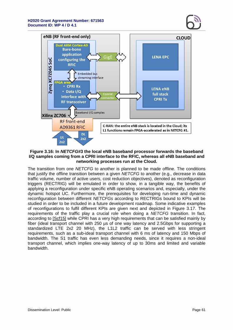
H2020 Grant Agreement Number: 671563 Document ID: WP 4 / D 4.1
Dissemination Level: Public Page 61
Figure 3.16: In NETCFG#3 the local eNB baseband processor forwards the baseband I/Q samples coming from a CPRI interface to the RFIC, whereas all eNB baseband and
networking processes run at the Cloud.
The transition from one NETCFG to another is planned to be made offline. The conditions that justify the offline transition between a given NETCFG to another (e.g., decrease in data traffic volume, number of active users, cost reduction objectives), denoted as reconfiguration triggers (RECTRIG) will be emulated in order to show, in a tangible way, the benefits of applying a reconfiguration under specific eNB operating scenarios and, especially, under the dynamic hotspot UC. Furthermore, the prerequisites for developing run-time and dynamic reconfiguration between different NETCFGs according to RECTRIGs bound to KPIs will be studied in order to be included in a future development roadmap. Some indicative examples of reconfigurations to fulfil different KPIs are given next and depicted in Figure 3.17. The requirements of the traffic play a crucial role when doing a NETCFG transition. In fact, according to [Scf15] while CPRI has a very high requirements that can be satisfied mainly by fiber (ideal transport channel with 250 µs of one way latency and 2.5Gbps for supporting a standardized LTE 2x2 20 MHz), the L1L2 traffic can be served with less stringent requirements, such as a sub-ideal transport channel with 6 ms of latency and 150 Mbps of bandwidth. The S1 traffic has even less demanding needs, since it requires a non-ideal transport channel, which implies one-way latency of up to 30ms and limited and variable bandwidth.

H2020 Grant Agreement Number: 671563 Document ID: WP 4 / D 4.1
Dissemination Level: Public Page 62
Figure 3.17: The three NETCFG and their relation with traffic capacity and latencies.
Reconfiguration from NETCFG#1 to NETCFG#2 or WCP modification [Scf15]:
Capacity/latency-aware14 reconfiguration: o As it can be seen in figure 3.17 if the demanded capacity increases or the latency
requirements become more stringent then by reconfiguring from NETCFG#1 to NETCFG#2, it would be possible to tackle this issue. Such conditions could apply when:
• There is a need to increase the signal bandwidth from 5 or 10 MHz to 20 MHz. • When there is a need to replace a SISO configuration with a MIMO scheme. • When there is a need to virtualize an eNB that will run in parallel with the
existing eNB (e.g., on-demand eNB infrastructure leasing to provide coverage to another operator).
Cost-aware reconfiguration: o When the daily cost of Cloud virtualization charged by Cloud providers to network
operators could be reduced (varying 24h charge) by leasing virtualization infrastructure from third parties with reduced tariffs at the specific time-slots of interest.
Reconfiguration from NETCFG#1 or 2 to NETCFG#3 [Scf15]:
Energy-aware reconfiguration: o Optimize the energy consumption at eNB level by switching them to a C-RAN
configuration. 14 Cloud services have been offered in core data centers (DCs) for high-computational or long-term processing. However, the cloud is being spread to the edge of the network (e.g., in edge DCs located in the metro network, or even in network nodes or mobile base stations with cloud capabilities) in order to reduce services’ latency to the end user. Variations of this concept are called MEC or fog computing.
H2020 Grant Agreement Number: 671563 Document ID: WP 4 / D 4.1
Dissemination Level: Public Page 63
3.3.1.3 Cognitive dynamic HW/SW partitioning algorithm
Motivation and objectives
The increasing network demands require new network services, higher performance, increased bandwidth, lower energy consumption and increased resilience. These demands imply a higher number of network devices and stations, increasing the cost and the energy consumption. The network centralization and functions virtualization become more significant as they enable better distribution of the available resources, less hardware utilization and an easier to upgrade network as current devices and architectures are meeting their limits. New implementation techniques must be introduced in order to further increase reusability, flexibility along with performance and energy consumption at the same time. According to this approach, the network functions can be moved to software as much as possible, without affecting networks latency. The functions virtualization can be achieved at any level, using a partitioning technique between software and hardware functions, which takes into account the available resources. The current network systems introduce a static and customized functions virtualization. This manual and static partitioning may lead to high performance but it is not reusable and not reconfigurable thus limiting network upgrades and resource allocation. Also, the processing power cannot be shared among nodes offering limited efficiency and spectrum capacity. Full virtualization is not always available as the devices of the underlying network might not be able of such a task, or virtualization might be limited according to available physical and computational resources. The cognitive dynamic HW/SW partitioning algorithm will provide reconfigurable and flexible HW/SW partitioning to both device and network element architectures in 5G technologies, considering high performance and energy consumption reduction, according to the specified performance scenarios. The HW/SW partitioning will be applicable for either inside a network stack layer and/or between multiple network stack layers, as shown in Figure 3.18:
Figure 3.18: Cognitive, dynamic HW/SW partitioning in network stack layers.
Problem statement
The partitioning technique must take into account a set of given network functions, the KPIs that have to be optimized and the KPI constraints relative to the available resources. The technique result has to provide the HW or SW implementation decision for each given function, according to the given policies. These policies consist of the KPIs and their constraints. The result of the implementation has to change according to the policies alteration. The cognitive dynamic HW/SW partitioning algorithm’s task is to provide the best

H2020 Grant Agreement Number: 671563 Document ID: WP 4 / D 4.1
Dissemination Level: Public Page 64
HW/SW partitioning of the 5G network stack functions, considering the given KPI’s per scenario and the available HW/SW resources.
Requirements
The algorithmic solution will provide an optimal implementation for a set of network functions according to the given KPIs, thus the selected technique is mostly referring to the architecture requirements of the Section 2. According to the above, the cognitive, dynamic HW/SW algorithm investigation is based on the following requirements:
Table 3.13 Architecture requirements.
ID Requirement Comment
IMPL-2 Adaptivity The ability to reconfigure the selected implementation when new requirements
are introduced.
ARCH-1 Overall latency The latency incurred by all components implemented in either in HW or SW,
communication between components and external interfaces.
ARCH-2 Reconfiguration overhead The time needed to switch from one device configuration to another.
ARCH-3 Energy-awareness The energy consumption of the selected HW components.
ARCH-4 Flexibility The degree of reusability of the selected HW/SW mixed model.
ARCH-5 Computational capacity The overall SW memory utilization.
ARCH-6 Scalability The scalability and upgradeability of the network architecture, obtained from
components reusability.
Problem general formulation
Functions definition
The proposed algorithmic solution provides dynamic performance optimization according to the specified scenarios, applicable to various network functions, leading to extended virtualization even on the lower network stack layers. To this approach the dynamic algorithmic solution can include new network functions that will be derived from future research. For the current research, the LTE 3GPP MAC layer functions can be considered as representative experimental basis for evaluation. A dataflow graph can be formed to represent the specified functions, their attributes and their connections. This graph will represent the block based model to be partitioned by the algorithmic solution.
KPIs definition
The partitioning algorithms task is to improve a high number of KPIs with the smallest amount of complexity, targeting a flexible and efficient design. The selected implementation must meet the constraints specified for the corresponding scenarios which include the following KPI’s:
Latency (LAT) in terms of: o Execution time of the whole model
Execution time when the function is implemented in SW Execution time when the function is implemented in HW
o Communication time (Between functions).
Energy efficiency (NRG): Referred to HW components consumption. It is contemporary to HW utilization.
Flexibility/reconfigurability (FVR) In terms of:

H2020 Grant Agreement Number: 671563 Document ID: WP 4 / D 4.1
Dissemination Level: Public Page 65
o Reusability: This means that a model is more reusable as less HW is used, thus this factor is inversely related to HW utilization.
Integration/size/footprint (ISF) in terms of: o SW memory usage: The memory needed when SW functions are executed
and running, relative to SW functions utilization.
User data rate (UDR) o The algorithm will take into account the user data rate limitations that are
introduced when there is need for more functions virtualization.
Optimization problem formulation
This approach introduces an optimization problem where each KPI is mapped to an equation that provides the relationship to the other KPIs. When a KPI value is minimized, another’s KPI value is increased. In order to specify this relationship the algorithm includes equations for each KPI with factors representing the relative difference. The proposed solution provides dynamic selection of the KPI to be further optimized, allowing different optimization selection according to the specified performance scenario. The above assumptions are summarized in the following formulation:
– N is the number of considered functions. – M is the number of considered KPIs. – x=[x1,...xN] is the decision variables vector, with xn, n = 1...N, representing HW
implementation (xn=1) or SW implementation (xn=0) of function n. – f(x) = [f1(x) ,...fM(x)] is the vector of objective functions to be minimized, each objective
function fm, m = 1...M, representing a corresponding KPI optimization. – fm(x)= a1mx1+....aNmxN, where, anm is the difference of the KPI m value between HW
implementation and SW implementation of function n. The factor anm is used to make the algorithm aware of the inverse relationship between the KPI’s.
– Each objective function fm, m = 1...M, can have a corresponding constraint, e.g. if m is the full model execution time-latency and it should be less than 80μs, this mean fm<=80.
– Each objective function fm, m = 1...M, can be normalized or prioritized by weights according to operator policies about the importance of KPI m.
Evolutionary Multi-objective Algorithmic solution
The partitioning algorithm will include a number of objective functions’ equations equal to the KPIs, that will be measured and optimized according to the given constraints. The algorithm has more than one optimization functions to consider thus a set of best solutions for every case must be produced. To this purpose, the algorithms that will be investigated are the evolutionary multi-objective algorithms:
Genetic algorithm NSGA II
Particle swarm optimization
Weighted sum method
Weighted metric method
These algorithms are very efficient but also of high complexity, thus the single-objective and lower complexity algorithms Simulated annealing and Tabu search are also under investigation. The result of the algorithmic solution can be a binary vector where each bit will represent a specified function and its value (“0”,”1”) will represent the implementation choice between hardware and software.
Functionality and communication
The algorithm’s result can be parsed to the management programs for further decision making on the implementation part. The algorithmic solution has to communicate with other programs to be aware of the available resources. Moreover the algorithm must be aware of
H2020 Grant Agreement Number: 671563 Document ID: WP 4 / D 4.1
Dissemination Level: Public Page 66
the performance scenario and the KPI constraints; thus the algorithm would interact with management programs and monitoring agents as seen in Figure 3.19.
Figure 3.19: Partitioning algorithm functionality and communication.
Demo prototype
The cognitive, dynamic HW/SW dynamic partitioning algorithm can support the 5G platforms reconfiguration, providing the optimal decision for HW or SW instantiation of the specified 5G network stack functions, according to corresponding scenario’s policies and context. To that purpose, there will be a sequence of demonstration activities, including a first, model based algorithmic evaluation demo of the partitioning algorithm applied on indicative models, without decision enforcement in implemented HW/SW functions. At the next step, there will be investigation for integrating decision enforcement in a specific number of implemented HW/SF functions, also trying to integrate with other Flex5Gware partners that can provide such new 5G targeting HW/SW functions.
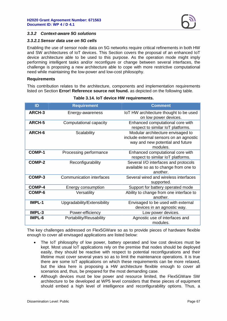
H2020 Grant Agreement Number: 671563 Document ID: WP 4 / D 4.1
Dissemination Level: Public Page 67
3.3.2 Context-aware 5G solutions
3.3.2.1 Sensor data use on 5G cells
Enabling the use of sensor node data on 5G networks require critical refinements in both HW and SW architectures of IoT devices. This Section covers the proposal of an enhanced IoT device architecture able to be used to this purpose. As the operation mode might imply performing intelligent tasks and/or reconfigure or change between several interfaces, the challenge is proposing a new architecture able to cope with more restrictive computational need while maintaining the low-power and low-cost philosophy.
Requirements
This contribution relates to the architecture, components and implementation requirements listed on Section Error! Reference source not found. as depicted on the following table.
Table 3.14. IoT device HW requirements.
ID Requirement Comment
ARCH-3 Energy-awareness IoT HW architecture thought to be used on low power devices.
ARCH-5 Computational capacity Enhanced computational core with respect to similar IoT platforms.
ARCH-6 Scalability Modular architecture envisaged to include external sensors on an agnostic
way and new potential and future modules.
COMP-1 Processing performance Enhanced computational core with respect to similar IoT platforms.
COMP-2 Reconfigurability Several I/O interfaces and protocols available so as to change from one to
another.
COMP-3 Communication interfaces Several wired and wireless interfaces supported.
COMP-4 Energy consumption Support for battery operated mode
COMP-6 Versatility Ability to change from one interface to another.
IMPL-1 Upgradability/Extensibility Envisaged to be used with external devices in an agnostic way.
IMPL-3 Power-efficiency Low power devices.
IMPL-6 Portability/Reusability Agnostic use of interfaces and modules.
The key challenges addressed on Flex5GWare so as to provide pieces of hardware flexible enough to cover all envisaged applications are listed below:
The IoT philosophy of low power, battery operated and low cost devices must be kept. Most usual IoT applications rely on the premise that nodes should be deployed easily, they should be reactive with respect to potential reconfigurations and their lifetime must cover several years so as to limit the maintenance operations. It is true there are some IoT applications on which these requirements can be more relaxed, but the idea here is proposing a HW architecture flexible enough to cover all scenarios and, thus, be prepared for the most demanding case.
Although devices must be low power and resource limited, the Flex5GWare SW architecture to be developed at WP5 level considers that these pieces of equipment should embed a high level of intelligence and reconfigurability options. Thus, a
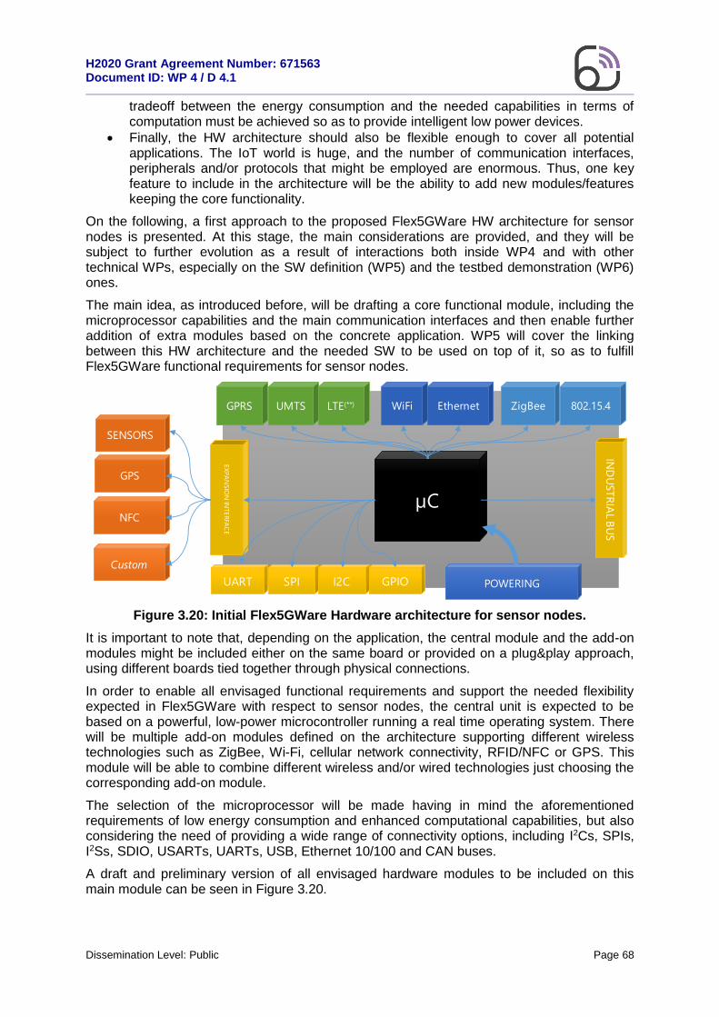
H2020 Grant Agreement Number: 671563 Document ID: WP 4 / D 4.1
Dissemination Level: Public Page 68
tradeoff between the energy consumption and the needed capabilities in terms of computation must be achieved so as to provide intelligent low power devices.
Finally, the HW architecture should also be flexible enough to cover all potential applications. The IoT world is huge, and the number of communication interfaces, peripherals and/or protocols that might be employed are enormous. Thus, one key feature to include in the architecture will be the ability to add new modules/features keeping the core functionality.
On the following, a first approach to the proposed Flex5GWare HW architecture for sensor nodes is presented. At this stage, the main considerations are provided, and they will be subject to further evolution as a result of interactions both inside WP4 and with other technical WPs, especially on the SW definition (WP5) and the testbed demonstration (WP6) ones.
The main idea, as introduced before, will be drafting a core functional module, including the microprocessor capabilities and the main communication interfaces and then enable further addition of extra modules based on the concrete application. WP5 will cover the linking between this HW architecture and the needed SW to be used on top of it, so as to fulfill Flex5GWare functional requirements for sensor nodes.
Figure 3.20: Initial Flex5GWare Hardware architecture for sensor nodes.
It is important to note that, depending on the application, the central module and the add-on modules might be included either on the same board or provided on a plug&play approach, using different boards tied together through physical connections.
In order to enable all envisaged functional requirements and support the needed flexibility expected in Flex5GWare with respect to sensor nodes, the central unit is expected to be based on a powerful, low-power microcontroller running a real time operating system. There will be multiple add-on modules defined on the architecture supporting different wireless technologies such as ZigBee, Wi-Fi, cellular network connectivity, RFID/NFC or GPS. This module will be able to combine different wireless and/or wired technologies just choosing the corresponding add-on module.
The selection of the microprocessor will be made having in mind the aforementioned requirements of low energy consumption and enhanced computational capabilities, but also considering the need of providing a wide range of connectivity options, including I2Cs, SPIs, I2Ss, SDIO, USARTs, UARTs, USB, Ethernet 10/100 and CAN buses.
A draft and preliminary version of all envisaged hardware modules to be included on this main module can be seen in Figure 3.20.
UART SPI I2C GPIO
µC
GPRS UMTS LTE(**) WiFi Ethernet ZigBee 802.15.4
EX
PA
NS
ION
INT
ER
FAC
E
IND
USTR
IAL B
US
POWERING
GPS
NFC
SENSORS
Custom

H2020 Grant Agreement Number: 671563 Document ID: WP 4 / D 4.1
Dissemination Level: Public Page 69
Figure 3.21. Flex5GWare sensor node HW architecture building blocks.
In addition to the main computational and communications module, the architecture will also cover, as mentioned before, add-on modules. These will cover three main areas:
Extended communication, by the use of either licensed (cellular modem) or unlicensed bands (ZigBee and Wi-Fi modules).
Positioning features with the GPS module.
Attaching external sensors, by enabling easy to use digital and analog inputs and outputs.
As an example, the architecture is expected to cover, initially the following HW add-on modules:
Cellular modem module. This module is one of the most important components that can be connected to the central module, as it guarantees long range connectivity and Internet access. The selection should be made based on requirements such as low-power consumption, small size and full Internet connectivity with native support of FTP and TCP/UDP protocols.
IoT specific radio interfaces (SigFox). In addition to long range cellular connectivity, the architecture should also cover the addition of radio modules able to join the new IoT networks, such as SigFox emerging, nowadays and offering very interesting operation modes for IoT devices.
NFC/RFID module. The NFC/RFID module should support several operating modes, as, for example, reader/writer roles, card emulation mode and peer-to-peer applications. This module is envisaged to be interoperable with most common standards, such as MIFARE, FeliCa, ISO/IEC 14443A&B and NFC (MIFARE Ultralight, MIFARE DESfire, Jewel, FeliCa and NFC smartphones) tags and cards.
GPS module. This module is expected to feature a very high sensitivity allowing satellite signal reception under extreme conditions. It should be also a low-power module that makes it suitable for battery operated mobile applications. It is expected to be used in extremely high dynamic applications.
Sensors Adapter. This module is oriented to ease the connection of sensors to the core module. The most common commercial sensors oriented to IoT applications provide their output either via analog variables (4-20 mA and/or 0-10V) or digital pins. This module will help translating from the general purpose sensor to the core module. Other common sensor interface is Serial/Modbus/RS485 interfaces. This module

H2020 Grant Agreement Number: 671563 Document ID: WP 4 / D 4.1
Dissemination Level: Public Page 70
should be flexible enough to also cover this functionality. This can be achieved by making use of dedicated UART ports.
Wi-Fi Module. The Wi-Fi module is expected to enable connectivity using 802.11b / g making it possible to exchange data at speeds of 54Mbps or faster, extending its possibilities to wireless data networks.
ZigBee module. ZigBee radio (or similar) use is very common on IoT applications, so as to form and maintain a wireless capillary network. Thus, the hardware architecture should be prepared to handle this kind of connectivity. At first glance, ZigBee seems the most appropriate interface to be used.
All aforementioned HW modules will enable the creation of a flexible, modular and comprehensive architecture for Flex5GWare sensor node modules, enabling the SW envisaged capabilities while keeping the overall IoT premises of low power and low cost devices.
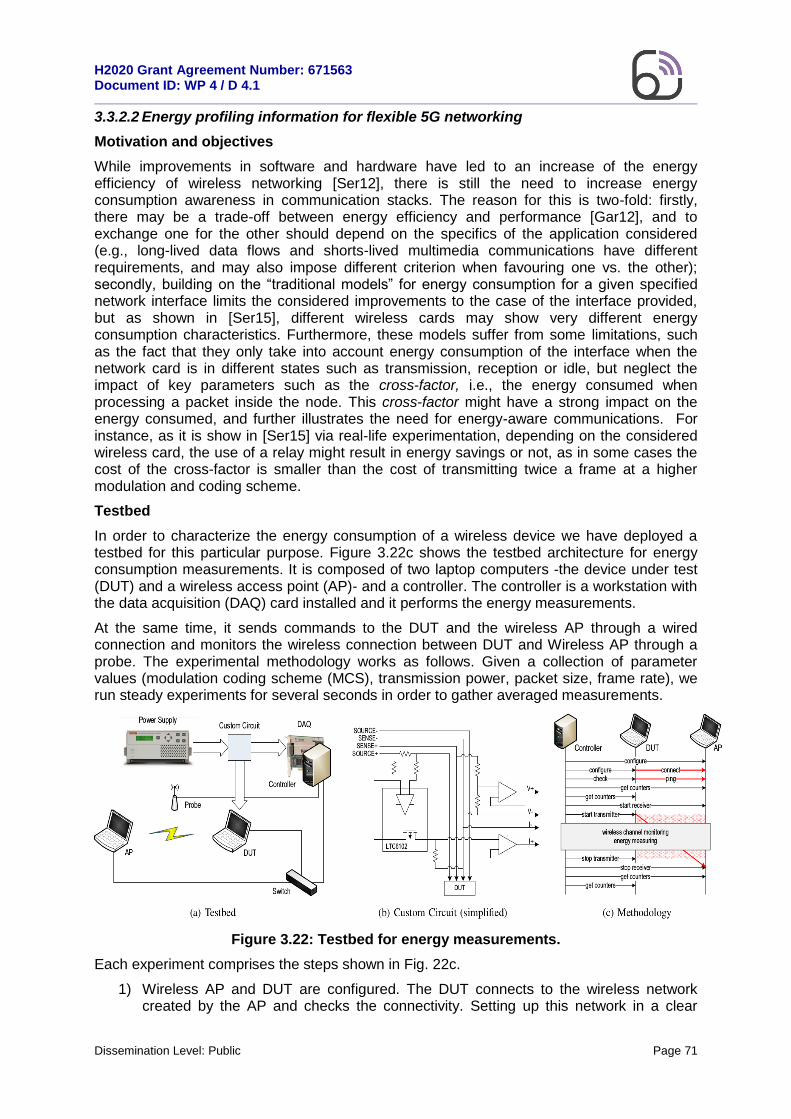
H2020 Grant Agreement Number: 671563 Document ID: WP 4 / D 4.1
Dissemination Level: Public Page 71
3.3.2.2 Energy profiling information for flexible 5G networking
Motivation and objectives
While improvements in software and hardware have led to an increase of the energy efficiency of wireless networking [Ser12], there is still the need to increase energy consumption awareness in communication stacks. The reason for this is two-fold: firstly, there may be a trade-off between energy efficiency and performance [Gar12], and to exchange one for the other should depend on the specifics of the application considered (e.g., long-lived data flows and shorts-lived multimedia communications have different requirements, and may also impose different criterion when favouring one vs. the other); secondly, building on the “traditional models” for energy consumption for a given specified network interface limits the considered improvements to the case of the interface provided, but as shown in [Ser15], different wireless cards may show very different energy consumption characteristics. Furthermore, these models suffer from some limitations, such as the fact that they only take into account energy consumption of the interface when the network card is in different states such as transmission, reception or idle, but neglect the impact of key parameters such as the cross-factor, i.e., the energy consumed when processing a packet inside the node. This cross-factor might have a strong impact on the energy consumed, and further illustrates the need for energy-aware communications. For instance, as it is show in [Ser15] via real-life experimentation, depending on the considered wireless card, the use of a relay might result in energy savings or not, as in some cases the cost of the cross-factor is smaller than the cost of transmitting twice a frame at a higher modulation and coding scheme.
Testbed
In order to characterize the energy consumption of a wireless device we have deployed a testbed for this particular purpose. Figure 3.22c shows the testbed architecture for energy consumption measurements. It is composed of two laptop computers -the device under test (DUT) and a wireless access point (AP)- and a controller. The controller is a workstation with the data acquisition (DAQ) card installed and it performs the energy measurements.
At the same time, it sends commands to the DUT and the wireless AP through a wired connection and monitors the wireless connection between DUT and Wireless AP through a probe. The experimental methodology works as follows. Given a collection of parameter values (modulation coding scheme (MCS), transmission power, packet size, frame rate), we run steady experiments for several seconds in order to gather averaged measurements.
Figure 3.22: Testbed for energy measurements.
Each experiment comprises the steps shown in Fig. 22c.
1) Wireless AP and DUT are configured. The DUT connects to the wireless network created by the AP and checks the connectivity. Setting up this network in a clear

H2020 Grant Agreement Number: 671563 Document ID: WP 4 / D 4.1
Dissemination Level: Public Page 72
channel is highly advisable to avoid interference. The 5 GHz band, with an 802.11a-capable card, is a good candidate.
2) The packet counters of the wireless interfaces are saved for later use.
3) Receiver and transmitter are started. We use the mgen 3 traffic generator and a simple netcat at the receiver.
4) The controller monitors the wireless channel and collects an energy trace that will be averaged later.
5) Transmitter and Receiver are stopped. 6) Because of the unreliability of the wireless medium, the packet counters, together
with the monitoring information, are used to ensure that the experiment was successful (i.e., the traffic seen agrees with the configured parameters).
Requirements
The following table presents the architecture requirements to implement the proposed system:
Table 3.15: Requirements
ID Requirement Comment
ARCH-2 Reconfiguration overhead The impact of changing several configuration over the network card
should be low in order to provide measurements in almost real-time.
ARCH-3 Energy-awareness The system takes into account the cross-factor of the device and profiles
the energy consumption by other factors.
ARCH-4 Flexibility The degrees of freedom in the moment of traffic generation to measure the
energy consumption and characterize the NIC.
COMP-4 Energy consumption The energy parameters of network card and the ability to set and modify
different MCS.
IMPL-2 Adaptivity The system implementation must be capable to measure different types of NIC such as Ethernet cards or IEEE
802.11 based-on cards.
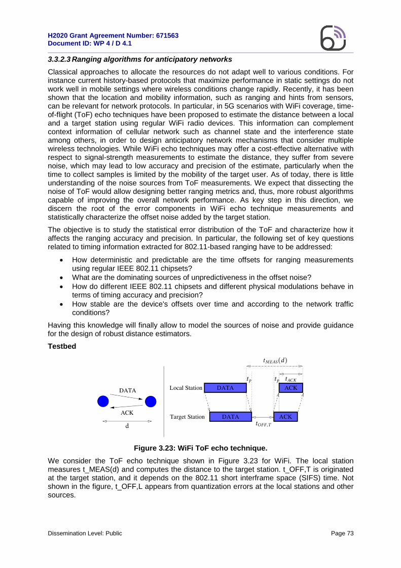
H2020 Grant Agreement Number: 671563 Document ID: WP 4 / D 4.1
Dissemination Level: Public Page 73
3.3.2.3 Ranging algorithms for anticipatory networks
Classical approaches to allocate the resources do not adapt well to various conditions. For instance current history-based protocols that maximize performance in static settings do not work well in mobile settings where wireless conditions change rapidly. Recently, it has been shown that the location and mobility information, such as ranging and hints from sensors, can be relevant for network protocols. In particular, in 5G scenarios with WiFi coverage, time-of-flight (ToF) echo techniques have been proposed to estimate the distance between a local and a target station using regular WiFi radio devices. This information can complement context information of cellular network such as channel state and the interference state among others, in order to design anticipatory network mechanisms that consider multiple wireless technologies. While WiFi echo techniques may offer a cost-effective alternative with respect to signal-strength measurements to estimate the distance, they suffer from severe noise, which may lead to low accuracy and precision of the estimate, particularly when the time to collect samples is limited by the mobility of the target user. As of today, there is little understanding of the noise sources from ToF measurements. We expect that dissecting the noise of ToF would allow designing better ranging metrics and, thus, more robust algorithms capable of improving the overall network performance. As key step in this direction, we discern the root of the error components in WiFi echo technique measurements and statistically characterize the offset noise added by the target station.
The objective is to study the statistical error distribution of the ToF and characterize how it affects the ranging accuracy and precision. In particular, the following set of key questions related to timing information extracted for 802.11-based ranging have to be addressed:
How deterministic and predictable are the time offsets for ranging measurements using regular IEEE 802.11 chipsets?
What are the dominating sources of unpredictiveness in the offset noise?
How do different IEEE 802.11 chipsets and different physical modulations behave in terms of timing accuracy and precision?
How stable are the device's offsets over time and according to the network traffic conditions?
Having this knowledge will finally allow to model the sources of noise and provide guidance for the design of robust distance estimators.
Testbed
Figure 3.23: WiFi ToF echo technique.
We consider the ToF echo technique shown in Figure 3.23 for WiFi. The local station measures t_MEAS(d) and computes the distance to the target station. t_OFF,T is originated at the target station, and it depends on the 802.11 short interframe space (SIFS) time. Not shown in the figure, t_OFF,L appears from quantization errors at the local stations and other sources.
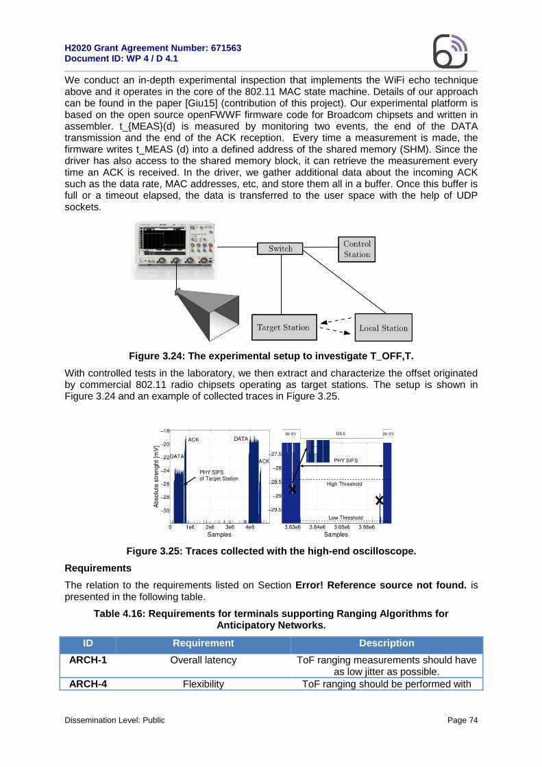
H2020 Grant Agreement Number: 671563 Document ID: WP 4 / D 4.1
Dissemination Level: Public Page 74
We conduct an in-depth experimental inspection that implements the WiFi echo technique above and it operates in the core of the 802.11 MAC state machine. Details of our approach can be found in the paper [Giu15] (contribution of this project). Our experimental platform is based on the open source openFWWF firmware code for Broadcom chipsets and written in assembler. t_{MEAS}(d) is measured by monitoring two events, the end of the DATA transmission and the end of the ACK reception. Every time a measurement is made, the firmware writes t_MEAS (d) into a defined address of the shared memory (SHM). Since the driver has also access to the shared memory block, it can retrieve the measurement every time an ACK is received. In the driver, we gather additional data about the incoming ACK such as the data rate, MAC addresses, etc, and store them all in a buffer. Once this buffer is full or a timeout elapsed, the data is transferred to the user space with the help of UDP sockets.
Figure 3.24: The experimental setup to investigate T_OFF,T.
With controlled tests in the laboratory, we then extract and characterize the offset originated by commercial 802.11 radio chipsets operating as target stations. The setup is shown in Figure 3.24 and an example of collected traces in Figure 3.25.
Figure 3.25: Traces collected with the high-end oscilloscope.
Requirements
The relation to the requirements listed on Section Error! Reference source not found. is presented in the following table.
Table 4.16: Requirements for terminals supporting Ranging Algorithms for Anticipatory Networks.
ID Requirement Description
ARCH-1 Overall latency ToF ranging measurements should have as low jitter as possible.
ARCH-4 Flexibility ToF ranging should be performed with
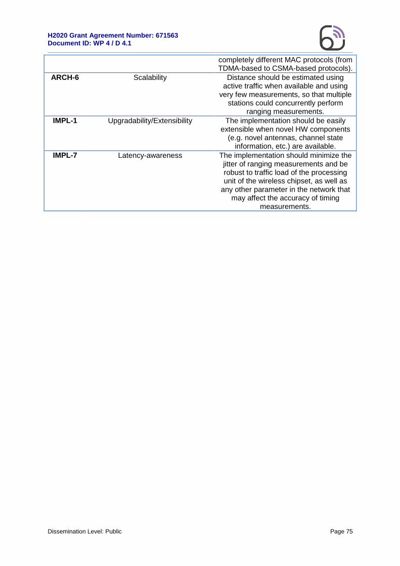
H2020 Grant Agreement Number: 671563 Document ID: WP 4 / D 4.1
Dissemination Level: Public Page 75
completely different MAC protocols (from TDMA-based to CSMA-based protocols).
ARCH-6 Scalability Distance should be estimated using active traffic when available and using
very few measurements, so that multiple stations could concurrently perform
ranging measurements.
IMPL-1 Upgradability/Extensibility The implementation should be easily extensible when novel HW components
(e.g. novel antennas, channel state information, etc.) are available.
IMPL-7 Latency-awareness The implementation should minimize the jitter of ranging measurements and be robust to traffic load of the processing unit of the wireless chipset, as well as
any other parameter in the network that may affect the accuracy of timing
measurements.

H2020 Grant Agreement Number: 671563 Document ID: WP 4 / D 4.1
Dissemination Level: Public Page 76
4. Conclusions
The goal of WP4 is to develop spectral efficient, energy efficient and flexible digital HW solutions. An important contribution of this deliverable is the definition of the digital HW requirements related to use cases and KPIs. For this purpose, the UCs and requirements defined in WP1 were analysed, forming likewise a basis to extract the requirements transferred to WP4. To this end, it was first conducted a high-level analysis of what each KPI means for the digital HW architectures of this WP. Three requirement categories were defined, covering the digital HW architecture, the digital HW components and the HW/SW implementation. The relation of each UC and KPI with the three requirement categories was defined in a coarse grain scale. Each category was then populated with a list of requirements. The idea is to reuse this requirement classification as a common reference for the different concepts presented in Section 3 and also in future deliverables and related documentation.
Taking into account the expertise of the partners involved in this WP, a number of key concepts have been selected to be implemented and validated in WP4. These concepts are either related to digital HW architectures optimising spectrum and energy efficiency or digital HW architectures optimising flexibility. Although the proposed concepts do not cover the entire 5G digital baseband development scope, they provide significant innovations at the digital front-end of 5G transceivers.
In more detail, for the solutions covering digital HW architectures that optimise spectral and energy efficiency, motivation, specifications, requirements and implementation objectives have been presented for the following concepts: FBMC structures for 5G (including waveform cohabitation with OFDM), new waveforms and MIMO equalization techniques, efficient high performance LDPC decoding, Turbo decoder design optimized for Massive IoT and finally optimum digital HW processing architectures for 5G network elements.
Furthermore, for the solutions covering digital HW architectures that optimise HW/SW flexibility, motivation, specifications, requirements and implementation objectives have been presented for the following concepts: an architecture for supporting MAC/PHY cross-layer reconfigurations, a flexible partitioning of SW and HW communication stack functions, a cognitive dynamic HW/SW partitioning algorithm, a modular architecture for sensor data use in 5G cells, an energy profiling framework for flexible 5G networking and finally ranging algorithms for anticipatory networks.
Finally it is important to highlight that synergies and complementarities of the concepts presented in WP4 were identified in Section 3.1.1. This might give space for further collaborations among partners, beyond the already planned in the context of WP6 PoCs.
H2020 Grant Agreement Number: 671563 Document ID: WP 4 / D 4.1
Dissemination Level: Public Page 77
5. References
[And14] Andrews, J.G.; Buzzi, S.; Wan Choi; Hanly, S.V.; Lozano, A.; Soong, A.C.K.; Zhang, J.C., “What Will 5G Be?,” in Selected Areas in Communications, IEEE Journal on , vol.32, no.6, pp.1065-1082, June 2014.
[Ban14] Banelli, P.; Buzzi, S.; Colavolpe, G.; Modenini, A.; Rusek, F.; Ugolini, A., “Modulation Formats and Waveforms for 5G Networks: Who Will Be the Heir of OFDM?: An overview of alternative modulation schemes for improved spectral efficiency,” in Signal Processing Magazine, IEEE , vol.31, no.6, pp.80-93, Nov. 2014.
[Bel01] M. Bellanger, “Specification and design of a prototype filter for filter bank based multicarrier transmission,” in Proceedings of the IEEE International Conference on Acoustics, Speech and Signal Processing, vol. 4, pp. 2417 – 2420, 2001.
[Ber14] V. Berg, J.-B. Dore, and D. Noguet, “A multiuser fbmc receiver implementation for asynchronous frequency division multiple access,” in Digital System Design (DSD), 2014 17th Euromicro Conference on, Aug 2014, pp. 16-21.
[Bon14] O. Boncalo, A. Amaricai, A. Hera, and V. Savin, “Cost Efficient FPGA Layered LDPC Decoder with Serial AP-LLR Processing”, IEEE International Conference on Field Programmable Logic and Applications (FPL), Munich, Germany, September 2014.
[Bou14] E. Boutillon and G. Masera, “Hardware Design and Realization for Iteratively Decodable Codes”, in Channel coding: Theory, algorithms, and applications, Academic Press Library in Mobile and Wireless Communications, Elsevier, June 2014.
[Dar08] A. Darabiha, A. C. Carusone, and F. R. Kschischang, “Power Reduction Techniques for LDPC Decoders”, IEEE Journal of Solid-State Circuits, vol. 43, no. 8, pp. 1835-1845, 2008.
[Dor14] J.-B. Doré, V. Berg, N. Cassiau, and D. Kténas, “FBMC receiver for multi-user asynchronous transmission on fragmented spectrum,” vol. 2014, 2014.
[Dzi14] A. Dziri, C. Alexandre, R. Zakaria, and D. Le Ruyet, “SDR-based prototype for filter bank based multi-carrier transmission,” in Wireless Communications Systems (ISWCS), 2014 11th International Symposium on, Aug 2014, pp. 878--882.
[Fet09] G. Fettweis, M. Krondorf, and S. Bittner, ``Gfdm - generalized frequency division multiplexing,'' in Vehicular Technology Conference, 2009. VTC Spring 2009. IEEE 69th, April 2009, pp. 1-4.
[Fon15] O. Font-Bach, N. Bartzoudis, A. Pascual-Iserte, M. Payaro, L. Blanco, D. López, M. Molina, “Interference Management in LTE-based HetNets: a Practical Approach”, Transactions on Emerging Telecommunications Technologies (Wiley), Vol. 26, Issue 2, Pages 195-215, February 2015, SN - 2161-3915.
[Fos04] M.P.C. Fossorier, “Quasicyclic Low-Density Parity-Check Codes from Circulant Permutation Matrices”, IEEE Trans. on Information Theory, vol. 50, no. 8, pp. 1788-1793, 2004.
[Gal63] R. G. Gallager, “Low-Density Parity-Check Codes”. Cambridge, MA:MIT Press, 1963.
[Gar12] A. Garcia-Saavedra, P. Serrano, A. Banchs, M. Hollick, “Balancing Energy Efficiency and Throughput Fairness in IEEE 802.11 WLANs”, Elsevier Pervasive and Mobile Computing, vol. 8, no. 5, October 2012.
H2020 Grant Agreement Number: 671563 Document ID: WP 4 / D 4.1
Dissemination Level: Public Page 78
[Giu15] D. Giustiniano, T. Bourchas, M. Bednarek, V. Lenders, “Deep Inspection of the Noise in WiFi Time-of-Flight Echo Techniques” MSWiM 2015 - The 18th ACM International Conference on Modeling, Analysis and Simulation of Wireless and Mobile Systems, 2-6 November 2015, Cancun, Mexico.
[Kam13] C. L. Kameni Ngassa, V. Savin, and D. Declercq “Design of Min-Sum-based LDPC decoders using imprecise arithmetic”, IEEE International Conference on Computer as a tool (EUROCON), Zagreb, Croatia, July 2013.
[Len90] T. Lengauer, “VLSI theory,” Handbook of theoretical computer science (vol. A): algorithms and complexity, pp. 835–866, 1990.
[Man02] M. M. Mansour and N. R. Shanbhag, “Low-power VLSI decoder architectures for LDPC codes,” in Proc. of International Symposium on Low Power Electronics and Design (ISLPED), Monterey, CA, pp. 284-289, Aug. 2002.
[Nad14] J. Nadal, C. Nour, A. Baghdadi, and H. Lin, “Hardware prototyping of fbmc/oqam baseband for 5g mobile communication,” in Rapid System Prototyping (RSP), 2014 25th IEEE International Symposium on, Oct 2014, pp. 72-77.
[Ngm15] NGMN Alliance, “5G White Paper,” February 2015, Available online at: https://www.ngmn.org/uploads/media/NGMN_5G_White_Paper_V1_0.pdf
[Ngu15] T. Nguyen-Ly, K. Le, F. Ghaffariy, A. Amaricai, O. Boncalo, V. Savin and D. Declercq, “FPGA Design of High Throughput LDPC Decoder based on Imprecise Offset Min-Sum Decoding”, IEEE International New Circuits And Systems Conference (NEWCAS), Grenoble, France, June 2015.
[Ric01] T. J. Richardson, M. A. Shokrollahi, and R. L. Urbanke, “Design of capacity-approaching irregular low-density parity-check codes," IEEE Trans. on Information Theory, vol. 47, no. 2, pp. 619-637, Feb 2001.
[Sav14] V. Savin, “LDPC decoders”, in Channel coding: Theory, algorithms, and applications, Academic Press Library in Mobile and Wireless Communications, Elsevier, June 2014.
[Scf15] “Small Cell Virtualization Functional Splits and Use Cases”, Small Cell Forum Release 5.1 (159.05.1.01), June 2015.
[Sch13] P. Schlafer, N. Wehn, M. Alles, and T. Lehnigk-Emden, “A New Dimension of Parallelism in Ultra High Throughput LDPC Decoding”, IEEE Workshop on Signal Processing Systems (SiPS), pp. 153-158, 2013.
[Ser12] P. Serrano, A. de la Oliva, P. Patras, V. Mancuso, A. Banchs, “Greening Wireless Communications: Status and Future Directions”, Elsevier Computer Communications, vol. 35, no. 14, August 2012 (Special Issue: Wireless Green Communications and Networking).
[Ser15] P. Serrano, A. Garcia-Saavedra, G. Bianchi, A. Banchs, A. Azcorra, "Per-Frame Energy Consumption in 802.11 Devices and Its Implication on Modeling and Design," in Networking, IEEE/ACM Transactions on , vol.23, no.4, pp.1243-1256, Aug. 2015.
[Spe99] M. Speth, S. Fechtel, G. Fock, and H. Meyr, ``Optimum receiver design for wireless broad-band systems using OFDM. i,'' vol. 47, no. 11, 1999, pp. 1668--1677.
[Tan81] R. M. Tanner, “A recursive approach to low complexity codes”, IEEE Transactions on Information Theory, vol. 27, no. 5, pp. 533-547, 1981.
[Vak13] V. Vakilian, T. Wild, F. Schaich, S. ten Brink, and J.-F. Frigon, ``Universal-filtered multi-carrier technique for wireless systems beyond lte,'' in Globecom Workshops (GC Wkshps), 2013 IEEE, Dec 2013, pp. 223-228.
H2020 Grant Agreement Number: 671563 Document ID: WP 4 / D 4.1
Dissemination Level: Public Page 79
[Wun13] G. Wunder et al., “5GNOW: Challenging the LTE design paradigms of orthogonality and synchronicity,” in Vehicular Technology Conference (VTC Spring), 2013 IEEE 77th, 2013.
[Wun14] G. Wunder et al., “5GNOW: Challenging the LTE design paradigms of orthogonality and synchronicity,” in IEEE Communications Magazine, 5G special issue, February 2014.
H2020 Grant Agreement Number: 671563 Document ID: WP 4 / D 4.1
Dissemination Level: Public Page 80
________________________________________________________________________
http://www.flex5gware.eu ________________________________________________________________________