Embed Size (px)
Citation preview

© 2000 Prentice Hall Inc.
Figure 5.1 n-Channel enhancement MOSFET showing channel length L and channel width W.
© 2000 Prentice Hall Inc.
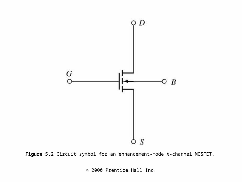
Figure 5.2 Circuit symbol for an enhancement-mode n-channel MOSFET.

© 2000 Prentice Hall Inc.
Figure 5.3 For vGS < Vto the pn junction between drain and body is reverse biased and iD=0.

© 2000 Prentice Hall Inc.
Figure 5.4 For vGS >Vto a channel of n-type material is induced in the region under the gate. As vGS increases, the channel becomes thicker. For small values of vDS ,iD is proportional to vDS.
The device behaves as a resistor whose value depends on vGS.

© 2000 Prentice Hall Inc.
Figure 5.5 As vDS increases, the channel pinches down at the drain end and iD increases more slowly. Finally for vDS> vGS -Vto, iD becomes constant.

© 2000 Prentice Hall Inc.
Figure 5.6 Characteristic curves for an NMOS transistor.

© 2000 Prentice Hall Inc.
Figure 5.7 This circuit can be used to plot drain characteristics.

© 2000 Prentice Hall Inc.
Figure 5.11 Drain characteristics for Example 5.2.

© 2000 Prentice Hall Inc.
Figure 5.12 Diodes protect the oxide layer from destruction by static electric charge.
© 2000 Prentice Hall Inc.
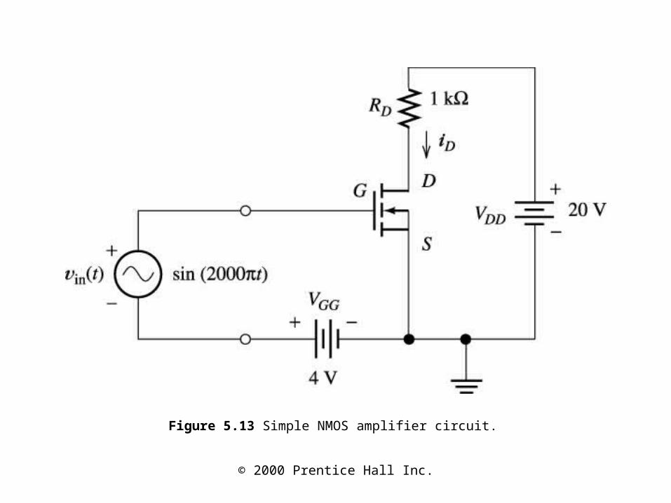
Figure 5.13 Simple NMOS amplifier circuit.
© 2000 Prentice Hall Inc.
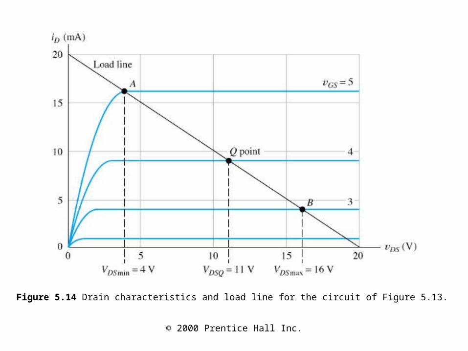
Figure 5.14 Drain characteristics and load line for the circuit of Figure 5.13.

© 2000 Prentice Hall Inc.
Figure 5.15 vDS versus time for the circuit of Figure 5.13.

© 2000 Prentice Hall Inc.
Figure 5.16 Fixed- plus self-bias circuit.

© 2000 Prentice Hall Inc.
Figure 5.17 Graphical solution of Equations (5.17) and (5.18).

© 2000 Prentice Hall Inc.
Figure 5.18 Fixed- plus self-biased circuit of Example 5.3.
© 2000 Prentice Hall Inc.
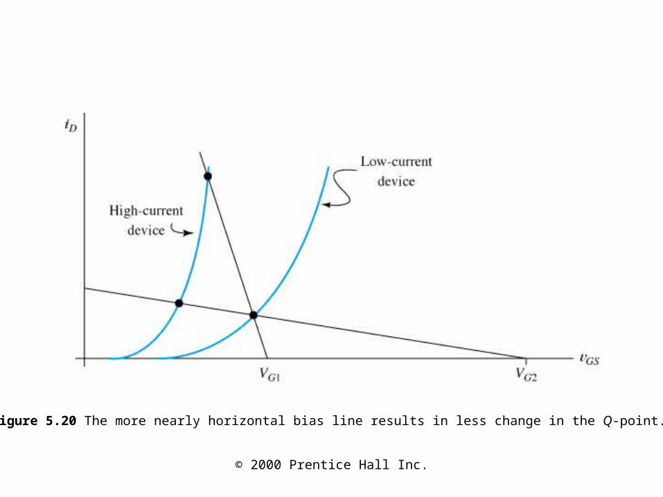
Figure 5.20 The more nearly horizontal bias line results in less change in the Q-point.

© 2000 Prentice Hall Inc.
Figure 5.21 Illustration of the terms in Equation (5.20).

© 2000 Prentice Hall Inc.
Figure 5.22 Small-signal equivalent circuit for FETs.
© 2000 Prentice Hall Inc.
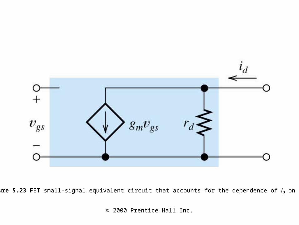
Figure 5.23 FET small-signal equivalent circuit that accounts for the dependence of iD on vDS.

© 2000 Prentice Hall Inc.
Figure 5.24 Determination of gm and rd. See Example 5.5.
© 2000 Prentice Hall Inc.
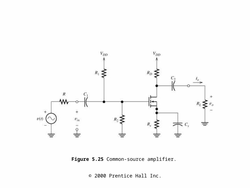
Figure 5.25 Common-source amplifier.
© 2000 Prentice Hall Inc.
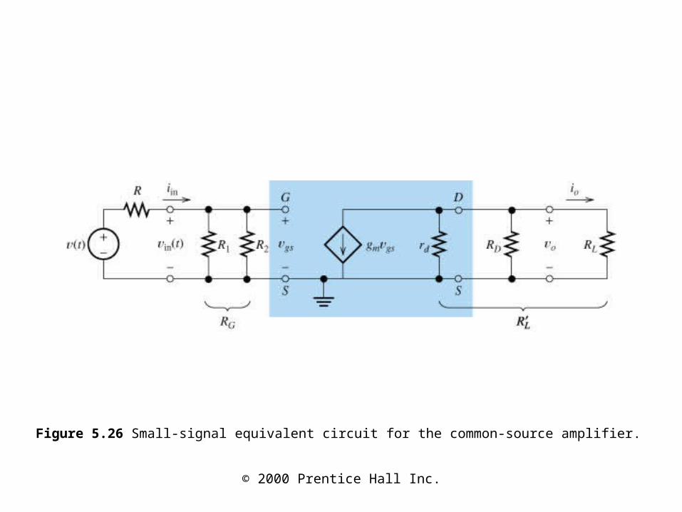
Figure 5.26 Small-signal equivalent circuit for the common-source amplifier.

© 2000 Prentice Hall Inc.
Figure 5.27 Circuit used to find $R_o$.

© 2000 Prentice Hall Inc.
Figure 5.28 Common-source amplifier.

© 2000 Prentice Hall Inc.
Figure 5.31 vo(t) and vin(t) versus time for the common-source amplifier of Figure 5.28.

© 2000 Prentice Hall Inc.
Figure 5.32 Gain magnitude versus frequency for the common-source amplifier of Figure 5.28.

© 2000 Prentice Hall Inc.
Figure 5.33 Source follower.

© 2000 Prentice Hall Inc.
Figure 5.34 Small-signal ac equivalent circuit for the source follower.
© 2000 Prentice Hall Inc.
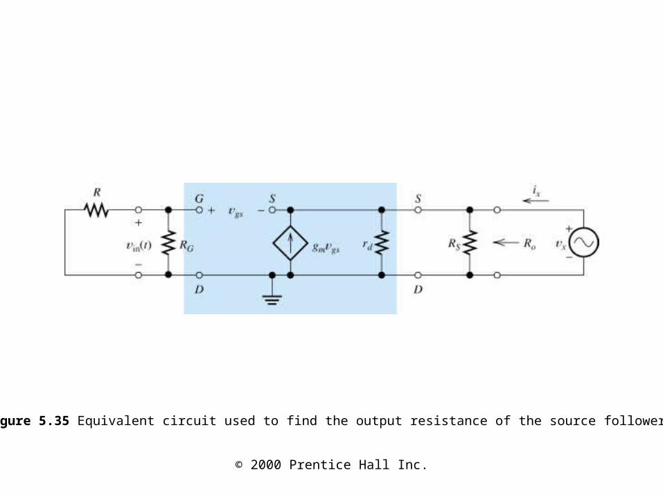
Figure 5.35 Equivalent circuit used to find the output resistance of the source follower.
© 2000 Prentice Hall Inc.
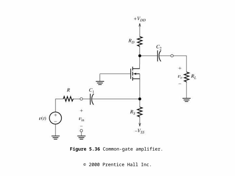
Figure 5.36 Common-gate amplifier.
© 2000 Prentice Hall Inc.
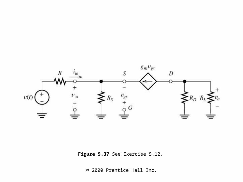
Figure 5.37 See Exercise 5.12.
© 2000 Prentice Hall Inc.
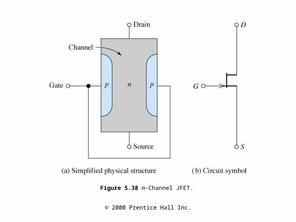
Figure 5.38 n-Channel JFET.

© 2000 Prentice Hall Inc.
Figure 5.39 The nonconductive depletion region becomes thicker with increased reverse bias. (Note: The two gate regions of each FET are connected to each other.)

© 2000 Prentice Hall Inc.
Figure 5.40 Circuit for the discussion of drain characteristics of the n-channel JFET.

© 2000 Prentice Hall Inc.
Figure 5.41 Drain current versus drain-to-source voltage for zero gate-to-source voltage.
© 2000 Prentice Hall Inc.
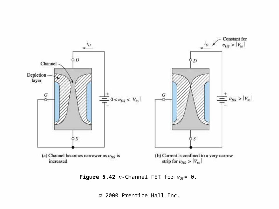
Figure 5.42 n-Channel FET for vGS = 0.

© 2000 Prentice Hall Inc.
Figure 5.43 Typical drain characteristics of an n-channel JFET.

© 2000 Prentice Hall Inc.
Figure 5.44 If vDG exceeds the breakdown voltage VB, drain current increases rapidly.

© 2000 Prentice Hall Inc.
Figure 5.45 See Exercise 5.14.
© 2000 Prentice Hall Inc.
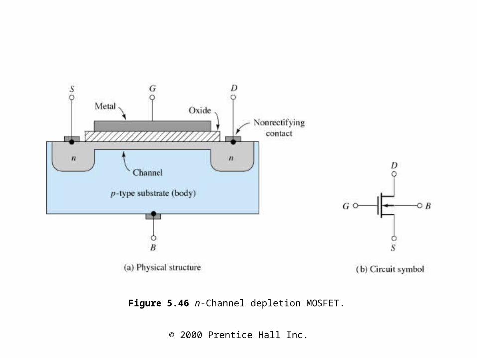
Figure 5.46 n-Channel depletion MOSFET.
© 2000 Prentice Hall Inc.
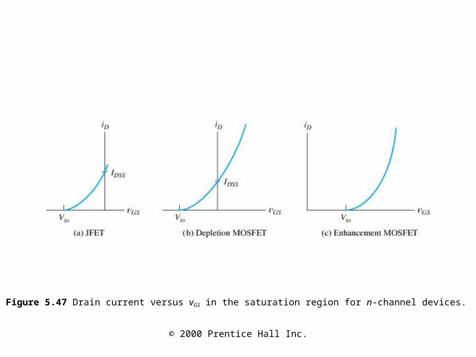
Figure 5.47 Drain current versus vGS in the saturation region for n-channel devices.

© 2000 Prentice Hall Inc.
Figure 5.48 p-Channel FET circuit symbols. These are the same as the circuit symbols for n-channel devices, except for the directions of the arrowheads.

© 2000 Prentice Hall Inc.
Figure 5.49 Drain current versus vGS for several types of FETs. iD is referenced into the drain terminal for n-channel devices and out of the drain for p-channel devices.