Embed Size (px)
Citation preview
Systematic Topology Derivation and PWM Design of Multilevel Converters
by
Yuzhuo Li
A thesis submitted in partial fulfillment of the requirements for the degree of
Doctor of Philosophy in
Energy System
Department of Electrical and Computer Engineering University of Alberta
© Yuzhuo Li, 2021
ii
Abstract Multilevel converters (MLCs) have been widely accepted for decades in various applications, e.g.
high-voltage transmission systems, medium-voltage drive systems, distributed generation inte-
grations, low voltage power supply, etc. During the evolution of power electronics equipment, a
large number of MLC topologies and pulse-width modulation (PWM) schemes are proposed. Due
to the sophisticated topology structure of MLCs, the topology derivation and PWM design meth-
ods are normally case-by-case and lack generality. While the concrete methods that emerged dur-
ing the development of MLCs are still ambiguous and lack systematic methodology.
At present, more new topologies keep emerging, resulting in a large number of circuits with
resembling structures and similar features which require systematic analysis and optimal design.
To better understand the relationship of various MLC topologies, the general relationships of
power converters are systematically discussed in this work, and new relationships are discovered
and elaborated, especially for the voltage-source converters (VSCs) and current-source converters
(CSCs). In addition to the famous duality principles, the novel isomorphic relationships of VSCs
and CSCs are firstly revealed in the power converter field with thorough theoretical discussions
and simulation/experimental verifications. To facilitate the derivation process of MLCs, the stage-
based uniform structures are also derived from the structure-level duality and the equivalence
and implemented for systematic topology synthesis and derivation for not only multilevel VSCs
and CSC, but also matrix converters. Several newly proposed topologies are demonstrated as ex-
amples with practical considerations and experiments on a special 5-level case.
To facilitate the PWM design process, a universal carrier-based PWM design method through
hierarchical method is proposed. It iteratively utilizes the identical circuits in converters and can
provide an exhaustive list of carrier-based PWM schemes for the non-modular MLCs, e.g. active-
neutral-point-clamped (ANPC) based converter. Based on this methodology, the novel phase shift
PWM for improvement of loss distribution, the systematic simplification of ANPC converters and

iii
systematic fault tolerant operation under multiple fault switches are also investigated, which also
has potentials for other ANPC-based derivatives. Various 4-level and 5-level PWM design cases
are elaborated with both theoretical investigations and experimental verifications in this work.
With the systematic knowledge of theory/circuit/structure/modulation level of MLCs, this
work will simplify the topology derivation and PWM design process over conventional case-by-
case methods and provide different innovation perspectives for MLC research.

iv
Acknowledgements
I would like to express my deep gratitude to all those who have offered valuable inspiration and
selfless support during my PhD program.
Firstly, I want to extend my heartfelt thanks to my supervisor, Professor Yunwei (Ryan) Li.
Without his encouragement and guidance, it would be impossible for this work to be accom-
plished. All the positive influences from him will be my great treasure in future life.
Secondly, for all the lab mates that have provided their professional suggestions, comments,
assistance, please accept my appreciation: Dr. Hao Tian, Dr. Zhongyi Quan, Dr. Ding Li, Fanxiu
Fang, Nie Hou, Cheng Xue, Mingzhe Wu, Rouzbeh Reza Ahrabi, Pasan Gunawardena Loku Het-
tige, Dulika Nayanasiri, Andrew Zhou Xuesong Wu, Xuerui Lin, etc. I am honored to study and
work with all of you, thank you!
Thirdly, my sincere thanks to all the teachers that have taught me. Without these valuable
knowledges, this work would have been impossible to begin with.
I would also to thank the financial support from China Scholarship Council.
Lastly, I want to thank my family for their understanding, patience, and love that make this
work possible.
v
Table of Contents
Chapter 1 Introduction ................................................................................................................ 1
1.1. Multilevel converters in the industry .......................................................................... 1
1.1.1 Multilevel converters for conventional applications ............................................... 1
1.1.2 MLCs for promising low-voltage applications ....................................................... 4
1.2. Multilevel converters research review ....................................................................... 6
1.2.1 Derivation methods of multilevel converters ..........................................................7
1.2.2 PWM design methods of multilevel converters ..................................................... 8
1.3. Circuit theory and graph theory in power electronics .............................................. 11
1.3.1 Duality methods .................................................................................................... 11
1.3.2 Graphical methods ................................................................................................ 13
1.3.3 Topology cycling phenomenon ............................................................................. 15
1.4. Research objectives and contributions ..................................................................... 16
Chapter 2 Fundamental relationships of power converters ..................................................... 20
2.1. Dual transformation ................................................................................................ 22
2.1.1 Dual transformation of planar circuit .................................................................. 23
2.1.2 Dual transformation of non-planar circuit .......................................................... 27
2.1.3 Summary of various duality-based methods ........................................................ 31
2.2. Isomorphic transformation ..................................................................................... 33
2.2.1 VSCs and CSCs transformation using the proposed isomorphic method ........... 34
2.2.2 Modulation transformation of VSCs and CSCs ................................................... 39
2.2.3 Potential applications .......................................................................................... 43
2.3. Topology cycling phenomenon ................................................................................ 44
2.3.1 Cycling phenomenon in power converters .......................................................... 45
2.3.2 Cycling rules for VSCs and CSCs ......................................................................... 48
2.3.3 Potential applications .......................................................................................... 52
2.4. Summary .................................................................................................................. 60
Chapter 3 Systematic derivation of multilevel converters ....................................................... 62
3.1. Unified models and structures of multilevel converters ......................................... 64
3.1.1 Structure-level relationships based on matrix models ........................................ 64
3.1.2 Stage-based structures of multilevel converters ................................................... 71
vi
3.1.3 Commonly used level generators, level selectors ................................................ 72
3.2. Synthesis of voltage-source and current-source multilevel converters ................... 78
3.2.1 Single-stage synthesis .......................................................................................... 79
3.2.2 Multiple-stage synthesis ...................................................................................... 84
3.2.3 Simplifications ..................................................................................................... 88
3.3. Generalization .......................................................................................................... 94
3.3.1 Matrix-type multilevel converters ....................................................................... 94
3.3.2 Cycling transformations for derivatives .............................................................. 97
3.4. Implementations and verifications ........................................................................ 100
3.4.1 Implementations of unified models ................................................................... 100
3.4.2 Inspirations of new topologies ........................................................................... 105
3.4.3 Practical considerations and verifications ........................................................ 109
3.5. Summary ................................................................................................................. 112
Chapter 4 Systematic PWM design of multilevel converters .................................................. 114
4.1. Topology features of ANPC-based converters ........................................................ 116
4.1.1 Identical circuits in MLCs ................................................................................... 116
4.1.2 Similarities of ANPC-based converters .............................................................. 119
4.1.3 Systematic PWM design procedure .................................................................... 122
4.2. Carrier-based PWM design examples ..................................................................... 129
4.2.1 Existing carrier-based PWM for 3L ANPC ......................................................... 129
4.2.2 Carrier-based PWM design for 4-level ANPC .................................................... 131
4.2.3 Carrier-based PWM design for 5-level ANPC .................................................... 134
4.2.4 Generalization and discussions .......................................................................... 136
4.3. Phase shift PWM design for ANPC-based converter .............................................. 139
4.3.1 Proposed phase shift PWM ................................................................................ 140
4.3.2 Phase shift PWM design examples ..................................................................... 144
4.3.3 Generalizations of the proposed method ........................................................... 147
4.3.4 Verifications and discussions ............................................................................. 150
4.4. Summary ................................................................................................................. 155
Chapter 5 Applications using the proposed unified models and PWM design approach ....... 157
5.1. Matrix models of ANPC converters ........................................................................ 159
5.1.1 General matrix model .......................................................................................... 159
5.1.2 Some special matrices ........................................................................................ 160
5.1.3 5L ANPC example ............................................................................................... 164
vii
5.2. Topology simplification method ............................................................................. 165
5.2.2 Hierarchical derivation of simplified ANPC converter ...................................... 167
5.2.3 Demonstration Examples ................................................................................... 169
5.2.4 Verifications........................................................................................................ 171
5.3. Fault-tolerant operation method ............................................................................ 174
5.3.1 Matrix models for fault-tolerant analysis ........................................................... 174
5.3.2 Systematic operation design ............................................................................... 179
5.3.4 Experimental verifications ................................................................................. 187
5.4. Summary ................................................................................................................. 192
Chapter 6 Conclusions and Future plans ................................................................................ 193
6.1. Achievements of this work ...................................................................................... 193
6.2. Interesting topics for future work ........................................................................... 196
References ....................................................................................................................................198
Appendix ...................................................................................................................................... 214
Appendix A: Matrix models of other MLCs .......................................................................... 214
Appendix B: Complete PWM patterns of 4-level ANPC converter ...................................... 216
Appendix C: Proof of the completeness of the PWM design method .................................. 217
Appendix D: Different switch groups for the general 4-level ANPC converter .................... 219
Appendix E: Different switch groups for the general 5-level ANPC converter ................... 220
viii
List of Tables
Table 2-I Ideal switches and their duals .................................................................................. 26
Table 2-II Dual relationships between voltage-source and current-source three-phase inverters
................................................................................................................................................... 28
Table 2-III Experiment Parameters ........................................................................................ 43
Table 2-IV Planar Circuits with Four-Step Topology Cycling Phenomenon ........................... 45
Table 2-V Nonplanar Circuits with Four-Step Topology Cycling Phenomenon ..................... 47
Table 2-VI Details of the Operation Analysis of Topology 13~16 ............................................ 53
Table 2-VII Input/Output Settings of Simulation ................................................................... 55
Table 2-VIII Experiment Settings of Topology 3 ..................................................................... 59
Table 3-I Summaries of Derived MLC Topologies (Per Phase) .............................................. 110
Table 3-II Experimental Parameters ....................................................................................... 111
Table 4-I Experimental Parameters ....................................................................................... 131
Table 4-II Switching Action Numbers of SCs in Three 4L Patterns in One Fundamental Period
.................................................................................................................................................. 138
Table 4-III Experiment Parameters ....................................................................................... 150
Table 4-IV Summary of the Proposed PS PWM and Conventional LS PWM Schemes for ANPC
Converters ................................................................................................................................ 154
Table 5-I Level Matrices of 3L PWM Patterns........................................................................ 167
Table 5-II Level Matrices of 4L-PWM-3-3-4 ..........................................................................168
Table 5-III Level Matrices of 4L-PWM-3-1-6 ......................................................................... 169
Table 5-IV Level Matrices of One of 5l PWM Patterns ........................................................... 171
Table 5-V Experimental Parameters ...................................................................................... 171
Table 5-VI The Eligibility of the Patterns through (5-41A) ....................................................184
Table 5-VII The Switches in HSF Cells with the Two Patterns .............................................. 185
Table 5-VIII The Summary of Various PWM Patterns ........................................................... 185
ix
List of Figures
Figure 1-1 Logic structure of Chapter 1. ........................................................................................... 1
Figure 1-2 Numbers of MLC papers published on IEEE Xplore (1990~2019). (Note that the numbers are obtained directly from the search results from IEEE Xplore and there could be a small number of unrelated papers.)...................................................................................... 3
Figure 1-3 Diversity of research topics of MLC papers published on IEEE Xplore (1990~2019).
(Note that all topics are obtained from the default setting from IEEE Xplore and there could be overlaps in some.) ............................................................................................................... 3
Figure 1-4 Classification of existing MLC topologies. ..................................................................... 4
Figure 1-5 Derivation methods of multilevel converters. ................................................................7
Figure 1-6 Modulation design methods of multilevel converters. .................................................. 9
Figure 1-7 The paradigm of power electronics shifts from triangle type to increasing diversity. . 11
Figure 1-8 Milestones of duality theory for electrical circuit and power converter....................... 13
Figure 1-9 Examples of isomorphic graphs. .................................................................................. 14
Figure 1-10 Research logic of this work. ........................................................................................ 19
Figure 2-1 Logic structure of Chapter 2. ........................................................................................ 21
Figure 2-2 (a) A simple demonstration circuit with controlled switch S. (b) Different drawings of the same electrical circuit. ..................................................................................................... 22
Figure 2-3 Duality between two different RLC resonance circuits [115], (a) RLC circuit with RL
series connection, (b) RLC circuit with RC parallel connection. ........................................... 23
Figure 2-4 Duality between two different RLC circuits with power source [116], (a) RLC circuit with series connection, (b) RLC circuit with parallel connection. ........................................ 24
Figure 2-5 Duality between two circuits with multiple meshes [116], (a) passive RLC circuit with active source, (b) the dual version of (a). .............................................................................. 24
Figure 2-6 (a) Mesh-type transformer and its equivalent electric circuit, (b) junction-type transformer and its equivalent electric circuit. ..................................................................... 25
Figure 2-7 Duality among switching DC-to-DC converters. ......................................................... 25
Figure 2-8 Duality between the buck and the boost switching converters. .................................. 26
Figure 2-9 An ideal transformer with the magnetizing inductance split, and its dual. ................ 26
Figure 2-10 Power circuit of a three-phase DC voltage link converter system. ............................ 27
x
Figure 2-11 Dual transformation of all eight switching states from DC voltage link converter to DC current link converter. ........................................................................................................... 27
Figure 2-12 Power circuit of a three-phase DC current link converter system. ............................ 28
Figure 2-13 Output equivalent circuits of (a) voltage-source and (b) current-source inverters. . 29
Figure 2-14 Input equivalent circuits of (a) voltage-source and (b) current-source inverters. .... 29
Figure 2-15 Julia’s physical dual method for a nonplanar circuit. (a) Original nonplanar circuit, (b) selected node A, (c) equivalent transformation through ideal transformer, (d) derived equivalent planar circuit, (e) implementation of conventional geometrical dual method, (f) derived dual circuit, (g) another dual circuit with 2-widing transformer, (h) derived dual
circuit if node D is chosen. ..................................................................................................... 29
Figure 2-16 Physical dual method through fictitious junction point for a nonplanar circuit. (a) Original nonplanar circuit, (b) introduced fictitious junction point through ideal transformer,
(c) the dual transformation, (d) implementation of fictitious junction point method for nonplanar circuit in Figure 17, (e) the dual transformation through strict dual method, (f) derived dual circuit. ............................................................................................................... 30
Figure 2-17 Constraints of an electric/magnetic node. (a) Constraint at a node of conductive wires,
(b) Constraint at a node of magnetic core. ............................................................................. 31
Figure 2-18 Analytical models of a resistor and a current source. (a) Magnetic model of resistance R, (b) Model of current source. ............................................................................................... 31
Figure 2-19 Dual topologies of a conventional non-planar three-phase VSC. (a) Non-planar three-phase CSC with three legs, (b) planar three-phase CSC with two legs and enabled through a three-phase transformer. ........................................................................................................ 31
Figure 2-20 Typical examples of power converters with non-planar circuits [11], [149], [150]. . 32
Figure 2-21 Applicable circuits types for different dual methods. ................................................ 32
Figure 2-22 Topology transformation process through duality. .................................................. 32
Figure 2-23 Different circuits can be obtained through the geometrical duals based on different
drawings of the same electrical circuit. ................................................................................. 33
Figure 2-24 The geometric graphs of typical power converters: (a) single-phase VSC Ga, (b) single-phase CSC Gb, (c) three-phase VSC Gc, (d) three-phase CSC Gd. .......................................... 35
Figure 2-25 Topology transformation process using isomorphism. ............................................ 37
Figure 2-26 Isomorphic transformation from a single-phase VSC to a single-phase CSC. .......... 37
Figure 2-27 Isomorphic transformation from a single-phase three-level T-type VSC to a three-phase CSC. ............................................................................................................................. 38
Figure 2-28 Isomorphic transformation from a single-phase multilevel T-type VSC to a multiphase CSC. ..................................................................................................................... 38
Figure 2-29 (a) Isomorphic transformation from single-phase three-level ANPC VSC and
associated three-phase CSC. (b) Isomorphic transformation from three-phase two-level VSC
xi
and an H-bridge multilevel CSC. (c) Isomorphic transformation from multiphase multilevel T-type VSC and multiphase multilevel CSC. (d) Isomorphic transformation from paralleled single-phase VSCs and single-phase CSCs. ........................................................................... 39
Figure 2-30 Space vector modulation diagrams of single-phase three-level T-type VSC and three-phase CSC derived from the isomorphic graph. .................................................................... 40
Figure 2-31 The one-to-one mapping of zero vectors between single-phase three-level T-type VSC and three-phase CSC derived from the isomorphic graph. ................................................... 40
Figure 2-32 Graph transformation from abc domain to max-mid-min domain. .......................... 41
Figure 2-33 (a) The algorithm of carrier-based PWM for VSC, (b) VSC main circuit. (c) The
algorithm of direct PWM for CSC, (d) CSC main circuit. ....................................................... 41
Figure 2-34 POD PWM waveforms and corresponding FFT results of Vp, Vn, and Vpn in (a) VSC, (b) CSC. PD PWM waveforms and corresponding FFT results of Vp, Vn, and Vpn in (c) VSC, (d)
CSC. ........................................................................................................................................ 42
Figure 2-35 (a) Experimental results of a three-phase IGCT-based CSC with Direct POD PWM. The 1st waveform (top) is the phase A current IA before filtered. The 2nd (middle) and 3rd (bottom) waveforms are DC voltage Vp and Vn with respect to the neutral point of three-phase
loads. (b) Waveforms of DC voltage Vp and Vn with respect to the middle phase voltage (after data processing in the max-mid-min domain). ..................................................................... 43
Figure 2-36 The theoretical waveforms (modulation index is 0.6) of four-phase CSC with carrier-
overlapped PWM developed from four-level VSC. ................................................................ 44
Figure 2-37 A reconfigurable CSC topology derived from four-leg VSC for DC-side fault. .......... 44
Figure 2-38 Cycling transformation phenomenon of power converters with H-bridge modules.46
Figure 2-39 Cycling transformation Example 3 of power converters with nonplanar circuits. ... 47
Figure 2-40 The general cycling transformation phenomenon of direct matrix converter. ........ 48
Figure 2-41 Multiple loops of converters and their drawings based on the dual and isomorphic method. (“Iso.” Stands for “isomorphic” in the figure.) ........................................................ 49
Figure 2-42 1-to-1 mapping of isomorphic transformation. ......................................................... 50
Figure 2-43 The general cycling transformation phenomenon of topology with n-port inputs and m-port outputs. (a) 2-step closed loop, (b) 4-step closed loop. ............................................ 52
Figure 2-44 The topological transformation cycling Example 3. ................................................. 54
Figure 2-45 Output waveforms of Topology 13~16. Line frequency is 60 Hz, modulation index is 0.9, equivalent switching frequency is 6k Hz. ....................................................................... 55
Figure 2-46 The switching signals implemented for Topology 13~16. ......................................... 55
Figure 2-47 FFT analysis results of (a) Idc of Topology 13 and Vdc of Topology 14, (b) Vac of Topology 15 and Iac of Topology 16. ....................................................................................................... 55
Figure 2-48 The simplified representation of Example 3. ............................................................ 56
xii
Figure 2-49 The switching functions of three topologies in Example 1. Topology 2: DC-parallel H-bridge VSCs. Topology 2: DC-series H-bridge CSCs. Topology 2: AC-series H-bridge VSCs. ............................................................................................................................................... 58
Figure 2-50 Implementation of carrier-based PWM for Topology 3. .......................................... 58
Figure 2-51 Experimental platform. ............................................................................................. 58
Figure 2-52 Implementation of carrier-based PWM for Topology 3. ........................................... 59
Figure 2-53 Harmonic spectrum of (a) Vac of Topology 3, (b) Vdc of Topology 3. ........................ 59
Figure 3-1 Logic structure of Chapter 3. ....................................................................................... 63
Figure 3-2 Half-bridge converter with two-level output. ............................................................. 65
Figure 3-3 H-bridge converter with three-level output. ............................................................... 65
Figure 3-4 Generalized MMC with half-bridge sub-module. (a) Circuit form. (b) Equivalent circuit form........................................................................................................................................ 66
Figure 3-5 Generalized self-balancing MLC. ................................................................................ 66
Figure 3-6 Single-phase single-rating inductor current-source MLC. ......................................... 67
Figure 3-7 H-bridge current-source inverter. ............................................................................... 67
Figure 3-8 3-level indirect matrix converter. ............................................................................... 69
Figure 3-9 Indirect matrix converter with 5L current output. ..................................................... 70
Figure 3-10 A generalized representation of multilevel topology based on the concept of the stage for (a) voltage-source MLC, (b) current-source MLC. ........................................................... 72
Figure 3-11 (a) Circuit form of the n-to-n level generator, (b) node-branch diagram of n-to-n level generator, (c) circuit form of the 1-to-n level generator, (d) node-branch diagram of the 1-to-n level generator. ................................................................................................................... 73
Figure 3-12 n-to-(n-1) level selector. (a) Circuit form. (b) Node-branch diagram. ...................... 74
Figure 3-13 n-to-1 level selector. (a) Circuit form. (b) Node-branch diagram. ............................ 74
Figure 3-14 (a) Simplification of one type LS into T-type LS circuits. (b) The equivalent function between two switching circuits. .............................................................................................. 75
Figure 3-15 1-to-n level generator for current-source MLC. (a) Circuit form. (b) Node-branch diagram. ................................................................................................................................. 76
Figure 3-16 n-to-1 level selector for current-source MLC. (a) Circuit form. (b) Node-branch diagram. .................................................................................................................................. 77
Figure 3-17 n-to-1 level selector for current-source MLC. (a) Circuit form. (b) Node-branch diagram. .................................................................................................................................. 77
Figure 3-18 1-to-n level selector for current-source MLC. (a) Circuit form. (b) Node-branch diagram. .................................................................................................................................. 77
xiii
Figure 3-19 The unified method of synthesis and derivation of MLCs. ........................................ 78
Figure 3-20 The process of node insertion for the voltage-source circuit. (a) Node-branch form. (b) Circuit form. ..................................................................................................................... 80
Figure 3-21 The process of node insertion for the current-source circuit. (a) Node-branch form. (b) Circuit form. ..................................................................................................................... 80
Figure 3-22 The process of branch split for the voltage-source circuit. (a) Node-branch form. (b)
Circuit form. ........................................................................................................................... 80
Figure 3-23 Other possible synthesis results. ................................................................................ 81
Figure 3-24 The process of branch split for the current-source circuit. (a) Node-branch form. (b) Circuit form. ............................................................................................................................ 81
Figure 3-25 The process of circuit expansion for the voltage-source converter. ........................... 81
Figure 3-26 The process of circuit expansion for the current-source converter. ......................... 82
Figure 3-27 The synthesis procedure of a single-stage circuit. ..................................................... 82
Figure 3-28 3L T-type stage. (a) Circuit form. (b) Synthesis process in node-branch form. ....... 83
Figure 3-29 4L ANPC stage with six switches. (a) Circuit form. (b) Synthesis process in node-branch form. .......................................................................................................................... 83
Figure 3-30 5L single-rating inductor current-source MLC stage. (a) Circuit form. (b) Synthesis process in node-branch form. ................................................................................................ 84
Figure 3-31 5L multi-rating inductor current-source MLC stage. ................................................ 84
Figure 3-32 Stand-alone stages. (a) 2-to-3 stage. (b) 3-to-2 stage. (c) 2-to-1 stage. .................... 85
Figure 3-33 3L bridge. (a) Circuit form. (b) Node-branch form. .................................................. 86
Figure 3-34 Stand-alone stages. (a) 1-to-2 stage. (b) 1-to-2 stage. ............................................... 87
Figure 3-35 5L current-source MLC. ............................................................................................ 87
Figure 3-36 The derivation procedure of a multiple stage circuit. ............................................... 87
Figure 3-37 (a) Single phase leg topology of hybrid clamped 3-level converter, (b) derivation of the hybrid clamped 3-level converter. ................................................................................... 88
Figure 3-38 Simplification process of a 9L converter. (a) Node-branch form. (b) Circuit form. . 90
Figure 3-39 Simplification process of a 5L converter. (a) Node-branch form. (b) Circuit form. . 92
Figure 3-40 Simplification process of a 5L converter. (a) Node-branch form. (b) Circuit form. . 93
Figure 3-41 Circuits with same three-pole switching function. .................................................... 94
Figure 3-42 (a) Eight-switch 5L ANPC converter. (b) Seven-switch 5L ANPC converter. ........... 94
Figure 3-43 Topologies of (a) direct matrix converter, (b) indirect matrix converter. ................ 95
Figure 3-44 Indirect matrix converter decomposed by voltage/current-source converter.......... 96
xiv
Figure 3-45 The derivation procedure of a matrix type MLC through the proposed method. ..... 96
Figure 3-46 3-level T-type NPC indirect matrix converter and its direct matrix counterpart. .... 97
Figure 3-47 The topological transformation loop for a known Topology X1 with unknown topologies to be discovered. (a) Two-step loop, (b) four-step loop. ...................................... 98
Figure 3-48 Topology derivation examples with planar circuits (the labels of topologies are named after the ones in chapter 2). ................................................................................................... 98
Figure 3-49 Topology derivation examples with nonplanar circuits. ........................................... 99
Figure 3-50 The generalized MLC topology synthesis and derivation flow chart. ...................... 101
Figure 3-51 Node-branch diagram of 5L-ANPC topology........................................................... 102
Figure 3-52 The augmented level generator of the 2nd stage of 5L-ANPC topology. ................ 102
Figure 3-53 The single stage node-branch diagram of 5L-ANPC topology. ............................... 104
Figure 3-54 Derivation process of a 4L T-type NNPC. ................................................................ 105
Figure 3-55 Derivation process of the internal parallel 3L ANPC. ............................................. 106
Figure 3-56 The modular structure of the internal parallel 3L ANPC. ....................................... 106
Figure 3-57 Derivation process of hybrid-clamped 7L topology (a) 7L 1# topology, (b) 7L 2# topology, (c) 7L 3# topology. ................................................................................................ 107
Figure 3-58 (a) PS-PWM for 3L flying capacitor converter, (b) PWM for hybrid-clamped 7L topology 1#. .......................................................................................................................... 108
Figure 3-59 Derivation process of two hybrid-clamped 9L topologies. ..................................... 108
Figure 3-60 Voltage balance of flying capacitors of hybrid-clamped 9L topology through (a) 2L balancing circuit for 9L 1# topology, (b) 3L balancing circuit for 9L 2# topology. ............ 109
Figure 3-61 Extended the second stage circuit into a generalized version to obtain higher output levels through (a) FCs with auxiliary circuit, (b) DC supplies. ............................................ 109
Figure 3-62 Experimental setup. .................................................................................................. 111
Figure 3-63 Experimental results of 2# topology example. The waveforms from top to bottom: output current of the A2 terminal, the output current of the total current, output PWM voltage
pulses. The RMS value of the current reference is changed from 4A to 8A during the operation. .............................................................................................................................................. 112
Figure 4-1 Logic structure of Chapter 4. ...................................................................................... 115
Figure 4-2 Topologies of some modular converters. ................................................................... 116
Figure 4-3 Topologies of some non-modular converters............................................................. 117
Figure 4-4 Topologies of the hybrid-clamped converters............................................................ 117
Figure 4-5 The classification of different identical circuits for multilevel converters. ................ 118
xv
Figure 4-6 The identical circuits within a single converter representing as symmetrical non-overlapping circuits in 3L NPC and 3L ANPC converters. ................................................... 118
Figure 4-7 The identical circuits within a single converter representing as asymmetrical non-overlapping circuits in simplified 3L ANPC converters. ...................................................... 118
Figure 4-8 All possible PWM patterns of 3L ANPC (a) 3L-PWM-1, (b) 3L-PWM-2, (c) 3L-PWM-3, (d) 3L-PWM-4, (e) 3L-PWM-5, (f) 3L-PWM-6, (g) 3L-PWM-7, (h) 3L-PWM-8. (i) Simplified representations of corresponding 3L PWM patterns. .......................................................... 119
Figure 4-9 The simplified graphical representations of ANPC-based converters with hybrid structures. (a) The 5-level hybrid clamped converter extended from 3L ANPC converter with 3L-PWM-1, (b) the simplified 5L ANPC converter extended from 3L ANPC converter with 3L-PWM-2. ................................................................................................................................ 120
Figure 4-10 Identical circuits in a conventional 5L ANPC converter. (a) Identical circuits between two converters, (b) some other identical circuits between two converters, (c)-(e) some non-overlapping identical 3L sub-topologies in a 5L ANPC converter, (f) overlapping identical 4L sub-topologies in a 5L ANPC converter, (g) overlapping identical 3L sub-topologies in a 5L ANPC converter. ................................................................................................................... 121
Figure 4-11 Three device utilization modes of 4L ANPC: (a) 4L-M1, (b) 4L-M2, (c) 4L-M3. ..... 123
Figure 4-12 Four device utilization modes of 5L ANPC: (a) 5L-M1, (b) 5L-M2, (c) 5L-M3, (d) 5L-M4. ........................................................................................................................................ 123
Figure 4-13 (a) 5L operation mode with SG2 operating at HSF, (b) 5L PWM pattern #1, (c) 5L PWM pattern #2, (d) 5L PWM pattern #3. .......................................................................... 124
Figure 4-14 The PWM design procedure based on hierarchical decomposition. ........................ 125
Figure 4-15 Hierarchical decomposition for ANPC-based topology. ........................................... 126
Figure 4-16 (a) Three first level decompositions of 4L ANPC topology, (b) two different topological decomposition examples of 5L topology, (c) two decomposition process results in the same decomposition of 5L topology. ............................................................................................. 126
Figure 4-17 Thirteen SG-based 4L PWM patterns. ...................................................................... 128
Figure 4-18 Carrier-based PWM for 3L ANPC under: (a) 3L-PWM-1, (b) 3L-PWM-2, (c) 3L-PWM-3, (d) 3L-PWM-4, (e) 3L-PWM-5. ........................................................................................ 129
Figure 4-19 Carrier-based PWM under (a) 4L-SG-1, (b) 4L-SG-3, (c) 4L-SG-9. ........................130
Figure 4-20 Single-phase 4L ANPC prototype. ........................................................................... 131
Figure 4-21 Experimental results of case 1~3. From top to bottom: gating signals of SC31, SC21, SC11, the PWM voltage of 4L ANPC converter. .................................................................... 132
Figure 4-22 Carrier-based PWM for 4L ANPC with pattern 4L-PWM-1-5-2. ............................. 133
Figure 4-23 Experimental results of case 4 (4L-PWM-1-5-2). From top to bottom: gating signals of SC31, SC22, SC11, the PWM voltage of 4L ANPC converter. ............................................ 133
xvi
Figure 4-24 FFT results of PWM voltages of (a) case 1, (b) case 2, (3) case 3, (4) case 4 with modulation index equals to 1. ............................................................................................... 133
Figure 4-25 Three SG-based 5L PWM patterns. .......................................................................... 134
Figure 4-26 Single-phase 5L ANPC prototype. ............................................................................ 134
Figure 4-27 Carrier-based PWM for 5L ANPC case 8. ................................................................. 135
Figure 4-28 Experimental results of case 5~7. From top to bottom: gating signals of SC41, SC31, SC11, the PWM voltage of 5L ANPC converter. .................................................................... 135
Figure 4-29 Experimental results of 5L ANPC case 8. From top to bottom: gating signals of SC41, SC31, SC22, the PWM voltage of 5L ANPC converter. ......................................................... 136
Figure 4-30 FFT results of PWM voltages of (a) case 5, (b) case 6, (3) case 7, (4) case 8 with modulation index equals to 1. ............................................................................................... 136
Figure 4-31 An N-level PWM pattern with only one HSF SC (SCn1) with a designed CB-PWM scheme (other cases are omitted here). ................................................................................ 137
Figure 4-32 Different allocations of HSF SCs in various PWM patterns. ................................... 138
Figure 4-33 Identical circuits in ANPC converter: (a)-(b) symmetrical overlapping identical sub-topologies, (c)-(d) asymmetrical non-overlapping identical sub-topologies. ..................... 140
Figure 4-34 Marx converters can be transformed into switch group in ANPC converters by eliminating the intermediate capacitors. (a) A two-stage Marx converter can be transformed into a sub-topology associated with two SCs, (b) a four-stage Marx converter can be
transformed into a sub-topology associated with four SCs. ................................................. 141
Figure 4-35 Phase-shifted PWM for (a) 2-stage upward switch group, (b) 3-level flying-capacitor bridge, (c) conventional H-bridge. ....................................................................................... 141
Figure 4-36 Phase-shifted PWM for (a) 3-stage upward switch group, (b) 4-stage upward switch group. .................................................................................................................................... 142
Figure 4-37 Phase-shifted PWM for (a) 2-stage downward switch group, (b) 3-stage downward switch group, (c) 4-stage downward switch group. .............................................................. 143
Figure 4-38 Phase-shift PWM Design Process for ANPC Converter. .......................................... 143
Figure 4-39 Phase-shift PWM for 3-level ANPC Converter......................................................... 144
Figure 4-40 Phase-shift PWM for the general 4-level ANPC converter. ..................................... 145
Figure 4-41 Phase-shift PWM for the general 5-level ANPC converter. ...................................... 147
Figure 4-42 The derivation of (n+1)-level ANPC topology by an n-level circuit. ........................148
Figure 4-43 Phase-shift PWM designed for (a) upward switch groups, (b) downward switch groups, (c) the combined PWM of n-level ANPC topology with multiple carrier groups. ................ 149
Figure 4-44 Experimental setups of 5L ANPC topology. ............................................................. 150
xvii
Figure 4-45 Three LS PWM schemes of the general 5L ANPC converter with different device utilizations. ........................................................................................................................... 151
Figure 4-46 The gating signals of switches [S5, S6, S7, S8, S9, S10], output PWM waveforms and load current of the general 5L ANPC converter using different PWM methods: (a) LS PWM 1, (b) LS PWM 2, (b) LS PWM 3, (b) the proposed PS PWM. (Modulation index from 0.9 to 0.45) ...................................................................................................................................... 151
Figure 4-47 FFT analysis of different PWM methods: (a) LS PWM scheme 1, (b) LS PWM scheme 2, (c) LS PWM scheme 3, (d) the proposed PWM scheme. .................................................. 152
Figure 4-48 (a) The output PWM waveforms of load change from 30mH/27.5Ω to 30mH/2.7Ω. (b) increased output power with higher DC-link voltage. .................................................... 152
Figure 4-49 Total losses of four different PWM schemes with (a) modulation index is 0.9, (b) modulation index is 0.45. ..................................................................................................... 153
Figure 4-50 Switching loss distributions of four different PWM schemes with (a) modulation index is 0.9, (b) modulation index is 0.45. ........................................................................... 153
Figure 5-1 Logic structure of Chapter 5. ...................................................................................... 158
Figure 5-2 General topology of (a) 3-level ANPC converter, (b) 4-level ANPC converter, (c) 5-level ANPC converter. ................................................................................................................... 159
Figure 5-3 5-level ANPC PWM patterns. (a) 5L-PWM-1, (b) 5L-PWM-2, (c) 5L-PWM-3, (d) 5L-PWM-4. ................................................................................................................................. 162
Figure 5-4 The carrier-based PWM generation and associated switching status of the upper switch of each SCs (same SG) of 5L-PWM-1. (a) value of one element in each status vectors, (b) blocking voltages in simulation. ........................................................................................... 162
Figure 5-5 The potential voltages of the three terminals of a single SC. ..................................... 163
Figure 5-6 (a)~(h) 3L PWM patterns, (i)~(j) derivations of simplified 3L ANPC converter. ..... 166
Figure 5-7 Three possible decompositions of 4L ANPC topology. ..............................................168
Figure 5-8 Derivations of simplified 4L ANPC converter based on existing simplified 3L ANPC converter. ..............................................................................................................................168
Figure 5-9 Derivations of simplified 4L ANPC converter through matrix models. ..................... 169
Figure 5-10 Derivations of simplified 5L ANPC converter through hierarchical decomposition. .............................................................................................................................................. 170
Figure 5-11 A simplified 4L ANPC topology based on 4L-PWM-3-1-2. ....................................... 172
Figure 5-12 Experimental results of (a) original 4L ANPC topology. (b) FFT analysis of original 4L converter PWM waveform. (c) simplified 4L ANPC topology. (b) FFT analysis of simplified
converter PWM waveform. ................................................................................................... 172
Figure 5-13 a simplified 5L ANPC topology based on 5L PWM pattern. ..................................... 173
xviii
Figure 5-14 Experimental results of (a) original 4L ANPC topology. (b) FFT analysis of original 4L converter PWM waveform. (c) simplified 4L ANPC topology. (b) FFT analysis of simplified converter PWM waveform. ................................................................................................... 173
Figure 5-15 Failures and causes for power switching devices. .................................................... 175
Figure 5-16 4-level ANPC converter with (a) operation range from L4 to L3, (b) operation range from L3 to L2, (c) operation range from L2 to L1................................................................. 176
Figure 5-17 The logic form values of se2 based on (4) by exhaustive investigation of associated states in 4-level topology (s'6 and s'4 are omitted since their values are complementary of s6 and s4, respectively). High level means logic value “1”, low level means logic value “0”. .... 177
Figure 5-18 (a) 4-level ANPC topology with three open-circuit switches (S1', S2', S4'). (b) The state matrix of the post-fault 4-level ANPC topology. .................................................................. 177
Figure 5-19 (a) Available switches for generation of 3rd and 4th voltage levels in 4-level ANPC under
normal condition. (b) One possible modulation scheme with S1, S1' operating at PWM frequency, other switches are maintained fix states. (c) Implementation of the modulation scheme in (b) with three switches (S1', S2', S4') are open-circuit. (d) Implementation of another modulation scheme with tolerance of open-circuit switches (S1', S2', S4'). ........................... 178
Figure 5-20 Post-fault 4-level ANPC with: (a) implementation of applicable scheme for generation of 2nd and 3rd voltage levels in, (b) implementation of applicable scheme for generation of 1st and 2nd voltage levels, (c) a PWM pattern that can guarantee a complete output capability. .............................................................................................................................................. 179
Figure 5-21 Flow chart of the proposed fault-tolerant operation for ANPC topology based on the matrix method. .................................................................................................................... 180
Figure 5-22 The device utilization of 5-level ANPC converter with (a) operation range from L5 to
L4, (b) operation range from L4 to L3, (c) operation range from L3 to L2, (d) operation range from L2 to L1. ......................................................................................................................... 182
Figure 5-23 Two PWM patterns with different arrangements of cells. ....................................... 183
Figure 5-24 Three fault cases with multiple open-circuit switches in 5-level ANPC topology. (a) Using pattern 1 under (a.1) fault case 1, (a.2) fault case 2, (a.3) fault case 3; (b) Using pattern 2 under (b.1) fault case 1, (b.2) fault case 2, (b.3) fault case 3. ............................................. 183
Figure 5-25 The detailed diagram of the PWM scheme designed for Pattern1. ..........................186
Figure 5-26 The detailed diagram of the PWM scheme designed for Pattern2. ..........................186
Figure 5-27 The single-phase 5-level experimental platform with the line frequency 60Hz, while the carrier/switching frequency is 1560Hz. The DC links of the converter are clamped by the DC power supply, and the total voltage is 120V. The RL load is chosen with value: 55ohm/30mH. ...................................................................................................................... 187
Figure 5-28 The fault case 1 with multiple open-circuit switches (s'5, s7) in 5-level ANPC topology: (a.1)-(a.4) using Pattern 1, (b.1)-(b.4) using Pattern 2. From left to right are the utilized switches during four operation regions covering all output levels, e.g. (a.1) is for [L5, L4], (a.2) is for [L4, L3], (a.3) is for [L3, L2], (a.4) is for [L2, L1]. ......................................................189
xix
Figure 5-29 Experimental results of 5L ANPC topology before and after open-circuit faults with implemented carrier-based PWM scheme under fault case 1 with (a) Pattern 1, (b) Pattern 2. Waveforms from top to bottom: switching states of S4', S5', S6, S7, S8, S10, the output PWM voltage, the load current. ......................................................................................................189
Figure 5-30 The fault case 2 with multiple open-circuit switches (s'5, s7, s'10) in 5-level ANPC topology: (a.1)-(a.4) using Pattern 1, (b.1)-(b.4) using Pattern 2. From left to right are the utilized switches during four operation regions covering all output levels, e.g. (a.1) is for [L5, L4], (a.2) is for [L4, L3], (a.3) is for [L3, L2], (a.4) is for [L2, L1]. ..................................... 190
Figure 5-31 Experimental results of 5L ANPC topology before and after open-circuit faults with implemented carrier-based PWM scheme under fault case 2 with (a) Pattern 1, (b) Pattern 2. Waveforms from top to bottom: switching states of S4', S5', S6, S7, S8, S10, the output PWM voltage, the load current. ..................................................................................................... 190
Figure 5-32 The fault case 3 with multiple open-circuit switches (s'5, s7, s'10) in 5-level ANPC topology: (a.1)-(a.4) using Pattern 1, (b.1)-(b.4) using Pattern 2. From left to right are the utilized switches during four operation regions covering all output levels, e.g. (a.1) is for [L5, L4], (a.2) is for [L4, L3], (a.3) is for [L3, L2], (a.4) is for [L2, L1]. ...................................... 191
Figure 5-33 Experimental results of 5L ANPC topology before and after open-circuit faults with implemented carrier-based PWM scheme under fault case 3 with (a) Pattern 1, (b) Pattern 2. Waveforms from top to bottom: switching states of S4', S5', S6, S7, S8, S10, the output PWM
voltage, the load current. ...................................................................................................... 191
xx
List of Abbreviations 3L Three Level
4L Four Level
5L Five Level
7L Seven Level
9L Nine Level
AC Alternating Current
ANPC Active Neutral Point Clamped
CCV Cyclo-Converter
CHB Cascaded H-Bridge
CSC Current-Source Converter
DC Direct Current
DMC Direct Matrix Converter
DPP Differential Power Processor
DSCC Double-Star Chopper Cell
EMI Electromagnetic Interference
EST Equivalent Switching Frequency
EV Electric Vehicle
FC Flying Capacitor
FCC Flying Capacitor Converter
FFT Fast Fourier Transform
GI Graph Isomorphism
GTO Gate Turn-Off Thyristor
HBBB H-Bridge Building Blocks
HSF High Switching Frequency
HV High Voltage
IC Integrated Circuit
IGCT Integrated Gate-Commutated Thyristor
IGBT Insulated Gate Bipolar Transistor
IMC Indirect Matrix Converter
KCL Kirchhoff’s Current Law
KVL Kirchhoff’s Voltage Law
xxi
LED Light-Emitting Diode
LS Level Selector
LS PWM Level-Shift PWM
LSF Low Switching Frequency
LG Level Generator
M.I Modulation Indexes
MLC Multilevel Converter
MMC Modular Multilevel Converter
MV Medium Voltage
NBD Node-Branch Diagram
NPC Neutral Point Clamped
NNPC Nested Neutral Point Clamped
NNPP Nested Neutral Point Piloted
PD Phase Disposition
POD Phase Opposition Disposition
PS PWM Phase-Shift PWM
PV Photovoltaic
PWM Pulse-Width Modulation
SC Switch Cell
SCR Silicon Controlled Rectifier
SG Switch Group
SMC Stacked Multicell Converter
SM Sub-Module
TNPC T-Type NPC
VSC Voltage-Source Converter
WBG Wide Bandgap
1
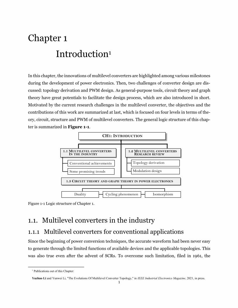
Chapter 1 Introduction1
In this chapter, the innovations of multilevel converters are highlighted among various milestones
during the development of power electronics. Then, two challenges of converter design are dis-
cussed: topology derivation and PWM design. As general-purpose tools, circuit theory and graph
theory have great potentials to facilitate the design process, which are also introduced in short.
Motivated by the current research challenges in the multilevel converter, the objectives and the
contributions of this work are summarized at last, which is focused on four levels in terms of the-
ory, circuit, structure and PWM of multilevel converters. The general logic structure of this chap-
ter is summarized in Figure 1-1.
1.2 MULTILEVEL CONVERTERS RESEARCH REVIEW
CH1: INTRODUCTION
1.1 MULTILEVEL CONVERTERS IN THE INDUSTRY
1.3 CIRCUIT THEORY AND GRAPH THEORY IN POWER ELECTRONICS
Topology derivation
Modulation design
Duality Cycling phenomenon Isomorphism
Conventional achievements
Some promising trends
Figure 1-1 Logic structure of Chapter 1.
1.1. Multilevel converters in the industry
1.1.1 Multilevel converters for conventional applications
Since the beginning of power conversion techniques, the accurate waveform had been never easy
to generate through the limited functions of available devices and the applicable topologies. This
was also true even after the advent of SCRs. To overcome such limitation, filed in 1961, the
1 Publications out of this Chapter: Yuzhuo Li and Yunwei Li, "The Evolutions Of Multilevel Converter Topology," in IEEE Industrial Electronics Magazine, 2021, in press.
2
magnetic coupling method was implemented to generate a multilevel voltage in the three-phase
system using square wave per module [1]. Filed in 1964, a similar idea was introduced for aircraft
applications, which featured lightweight, low harmonic distortion, and high efficiency [2]. Later,
in 1969, McMurray filed the patent for a stepped-wave converter which can be considered as the
predecessor of well-known cascaded H-bridge (CHB) converters [3]. And then, this topology was
perfected by the following researchers and resulted in the “modern” CHB converters at present
[4], [5]. Meanwhile, more topologies were developed featuring the multilevel outputs, such as
neutral-point-clamped converter [6], [7], flying capacitor-clamped (FCC) converter [8], active
neutral-point-clamped converter [9], modular multilevel converter[10], hybrid-clamped con-
verter [11], etc.
On the other hand, high-power devices like thyristor and GTO are commonly adopted for tra-
ditional CSCs [12]. Another commonly used device is IGCT, which has an even current distribu-
tion in the silicone and enhanced reliability due to redundant stages when connected in series [13].
Though the devices in CSCs require the reverse voltage blocking capability, the inherent lower
dv/dt, easier short-circuit protection and controllable regeneration features led this type con-
verter very popular for utility-scale power transmission and high-power drives [12]. However,
compared to the thriving VSCs covering applications in almost all the power levels, the behind-
hand performance of switching devices and bulky DC chokes makes CSCs struggle to expand their
applications, which in turn, results in relatively low interests on developing new CSCs. Recently,
advanced active/passive devices are emerging and have been applied in practice [14], as well as
show some promising development of CSCs penetrating the territory of VSCs [15]-[17].
Historically, the multilevel concept has been introduced in a more general way for the very early
stage of direct AC-AC converters, e.g. three-to-single-phase cyclo-converter (CCV) [18], [19]. The
approach of a practical CCV that synthesizes the AC output waveforms by actively selecting the
proper multiple AC inputs in predefined operational sectors is fundamentally the same as the
present MLCs (with “AC inputs” replaced by “DC inputs”) [19], [20]. Around the 1980s, the excel-
lence of CCVs in certain power ratings (e.g. MW-scale or lower) was challenged by the upcoming
matrix converters and other two-stage AC-AC configurations, e.g. back-to-back VSCs [12], [21].
The conventional matrix converters burst out in fierce market competition, however, end up with
desolate commercialization [22]. Recently, following the similar paths of VSCs and CSCs, some
“old-fashion” matrix topologies integrated with WBG devices are gaining increasing attention
thanks to component-level improvements and more advanced design [23], [24].
As of today, various MLCs have been widely applied in the industry owing to their merits like
high-quality output, reduced voltage/current stress on semiconductor devices, reduced device
3
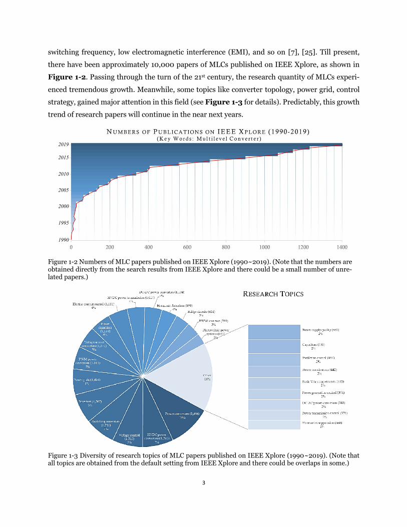
switching frequency, low electromagnetic interference (EMI), and so on [7], [25]. Till present,
there have been approximately 10,000 papers of MLCs published on IEEE Xplore, as shown in
Figure 1-2. Passing through the turn of the 21st century, the research quantity of MLCs experi-
enced tremendous growth. Meanwhile, some topics like converter topology, power grid, control
strategy, gained major attention in this field (see Figure 1-3 for details). Predictably, this growth
trend of research papers will continue in the near next years.
2019
1990
2005
1995
2000
2010
2015
Figure 1-2 Numbers of MLC papers published on IEEE Xplore (1990~2019). (Note that the numbers are obtained directly from the search results from IEEE Xplore and there could be a small number of unre-lated papers.)
Figure 1-3 Diversity of research topics of MLC papers published on IEEE Xplore (1990~2019). (Note that all topics are obtained from the default setting from IEEE Xplore and there could be overlaps in some.)
4
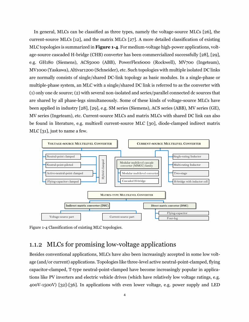
In general, MLCs can be classified as three types, namely the voltage-source MLCs [26], the
current-source MLCs [12], and the matrix MLCs [27]. A more detailed classification of existing
MLC topologies is summarized in Figure 1-4. For medium-voltage high-power applications, volt-
age-source cascaded H-bridge (CHB) converter has been commercialized successfully [28], [29],
e.g. GH180 (Siemens), ACS5000 (ABB), PowerFlex6000 (Rockwell), MV700 (Ingeteam),
MV1000 (Yaskawa), Altivar1200 (Schneider), etc. Such topologies with multiple isolated DC links
are normally consists of single/shared DC-link topology as basic modules. In a single-phase or
multiple-phase system, an MLC with a single/shared DC link is referred to as the converter with
(1) only one dc source; (2) with several non-isolated and series/parallel connected dc sources that
are shared by all phase-legs simultaneously. Some of these kinds of voltage-source MLCs have
been applied in industry [28], [29], e.g. SM series (Siemens), ACS series (ABB), MV series (GE),
MV series (Ingeteam), etc. Current-source MLCs and matrix MLCs with shared DC link can also
be found in literature, e.g. multicell current-source MLC [30], diode-clamped indirect matrix
MLC [31], just to name a few.
VOLTAGE-SOURCE MULTILEVEL CONVERTER
Neutral-point clamped
Neutral-point-piloted
Hyb
rid
clam
ped
Active-neutral-point clamped
Flying-capacitor clamped
CURRENT-SOURCE MULTILEVEL CONVERTER
Modular multilevel cascade converter (MMCC) family
Modular multilevel converter
Cascaded H-bridge
Single-rating Inductor
Multi-rating Inductor
Two-stage
H-bridge with inductor cell
MATRIX-TYPE MULTILEVEL CONVERTER
Indirect matrix converter (IMC) Direct matrix converter (DMC)
Voltage-source part Current-source part Flying-capacitor
Four-leg
Figure 1-4 Classification of existing MLC topologies.
1.1.2 MLCs for promising low-voltage applications
Besides conventional applications, MLCs have also been increasingly accepted in some low volt-
age (and/or current) applications. Topologies like three-level active neutral-point-clamped, flying
capacitor-clamped, T-type neutral-point-clamped have become increasingly popular in applica-
tions like PV inverters and electric vehicle drives (which have relatively low voltage ratings, e.g.
400V-1500V) [32]-[36]. In applications with even lower voltage, e.g. power supply and LED
5
driver, MLCs are also gaining their popularity [37]. Recent technology can even integrate multi-
level converter into integrated circuits [38]-[40].
Looking back into the history of power conversion techniques, the multilevel concepts have
been already proposed for some high-performance applications (e.g. lightweight, high efficiency,
reduced cost, etc.) since the very early stage of power electronics. The use of combinations of ca-
pacitors for producing high voltages can be traced back to the 19th century [41]. Such a technique
is one of the iconic features of modern MLCs. In 1863, the Hungarian physicist, Ányos Jedlik,
introduced the first voltage multiplying capacitor battery system, which can be considered as the
origin of the “switched capacitor” technique and was named as “chain of Leyden jars” back then
[42].
Sixty years later, in 1923, the Marx generator was invented for the R&D of lightening through
the same concept, but with different device technique [43]. Though this type of topologies was
implemented in extremely high voltage fields at first (prior 1950s), the shrink of their volume
happened soon after the advent of semiconductor-based switches [43]. The miniaturization of
commercial electronic equipment drove the inductor-less power conversion into surprisingly high
density and efficiency. Even now, it is not difficult to see the gene of the Marx generator in some
modern MLCs, e.g. derivatives of MMC [44], PV inverter [45], ANPC converter [46], etc. In recent
years, switched-capacitor-based MLCs are emerging in the literature to achieve reduced circuit
complexity and decent performance [47]. Some of them also feature the voltage self-balancing
and voltage boosting capability to cope with the high input-output voltage ratio within a single
power conversion stage [48], [49]. Yet, the core ideas have not been much evolved since the early
era of this technique, i.e. a similar methodology can be found in Baker’s patent filed in 1977 [50].
Moving forward from the pre-SCR period, another type of MLCs using a magnetic coupling
technique was introduced. For instance, Amato’s patent filed in 1960 managed to generate a five-
level stepwise waveform by utilizing a multi-switch structure [51]. It targeted portable applica-
tions with a potential lighter weight, smaller size, higher efficiency, and lower harmonic distor-
tions. Other examples are Heinrich’s patent filed in 1961 [52], Garnett’s patent filed in 1964 [2],
and Nard’s patent filed in 1967 [53], which were invented for similar reasons. Nearly 50 years
later of Amato’s patent, the in-leg magnetic coupling technique was introduced as another ap-
proach for multilevel waveform synthesis [54]. Another way is to use the interleaved technique,
like the multiphase MLC system introduced in 1962 [55], or the motor drive system in 1983 [56].
Essentially, the same method could also be found in some emerging MLCs [57], [58]. Recently,
the interleaved technique is further generalized by introducing the internal parallel concept in
MLCs [59], [60].
6
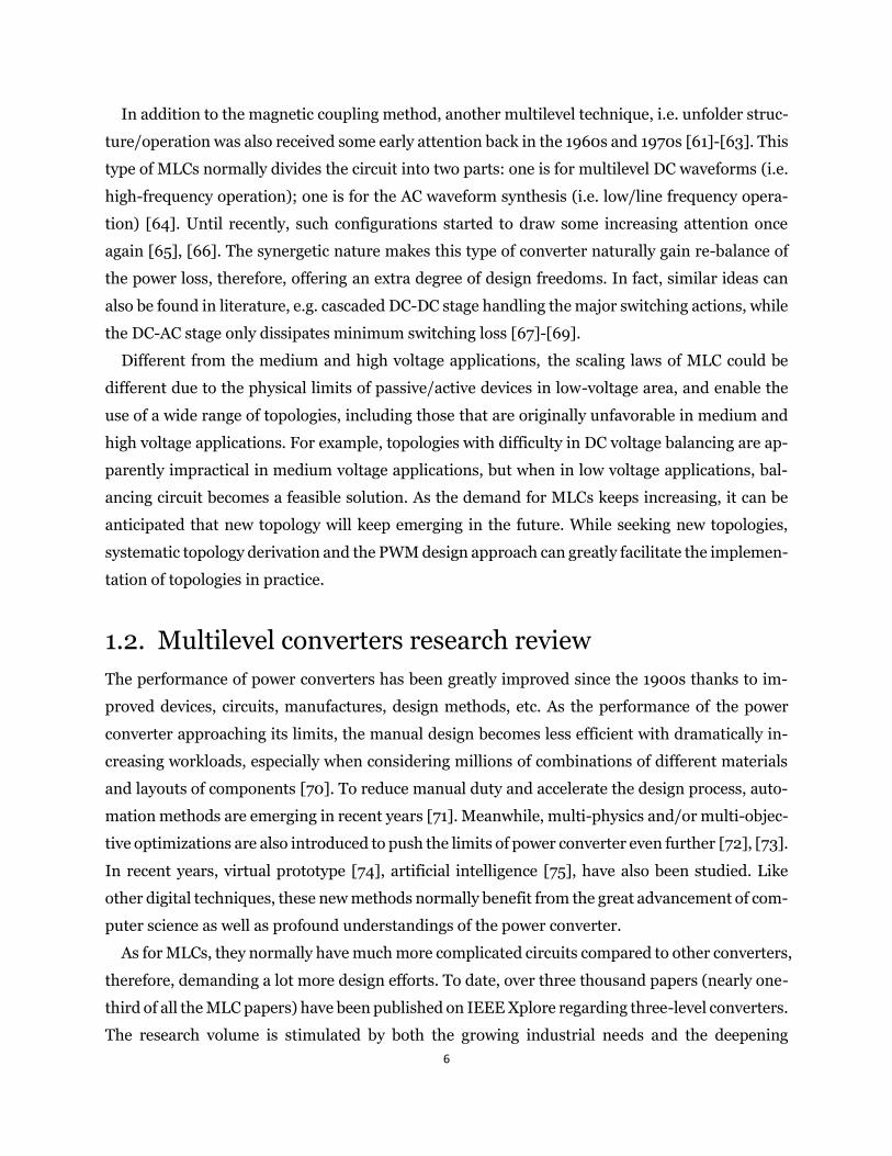
In addition to the magnetic coupling method, another multilevel technique, i.e. unfolder struc-
ture/operation was also received some early attention back in the 1960s and 1970s [61]-[63]. This
type of MLCs normally divides the circuit into two parts: one is for multilevel DC waveforms (i.e.
high-frequency operation); one is for the AC waveform synthesis (i.e. low/line frequency opera-
tion) [64]. Until recently, such configurations started to draw some increasing attention once
again [65], [66]. The synergetic nature makes this type of converter naturally gain re-balance of
the power loss, therefore, offering an extra degree of design freedoms. In fact, similar ideas can
also be found in literature, e.g. cascaded DC-DC stage handling the major switching actions, while
the DC-AC stage only dissipates minimum switching loss [67]-[69].
Different from the medium and high voltage applications, the scaling laws of MLC could be
different due to the physical limits of passive/active devices in low-voltage area, and enable the
use of a wide range of topologies, including those that are originally unfavorable in medium and
high voltage applications. For example, topologies with difficulty in DC voltage balancing are ap-
parently impractical in medium voltage applications, but when in low voltage applications, bal-
ancing circuit becomes a feasible solution. As the demand for MLCs keeps increasing, it can be
anticipated that new topology will keep emerging in the future. While seeking new topologies,
systematic topology derivation and the PWM design approach can greatly facilitate the implemen-
tation of topologies in practice.
1.2. Multilevel converters research review
The performance of power converters has been greatly improved since the 1900s thanks to im-
proved devices, circuits, manufactures, design methods, etc. As the performance of the power
converter approaching its limits, the manual design becomes less efficient with dramatically in-
creasing workloads, especially when considering millions of combinations of different materials
and layouts of components [70]. To reduce manual duty and accelerate the design process, auto-
mation methods are emerging in recent years [71]. Meanwhile, multi-physics and/or multi-objec-
tive optimizations are also introduced to push the limits of power converter even further [72], [73].
In recent years, virtual prototype [74], artificial intelligence [75], have also been studied. Like
other digital techniques, these new methods normally benefit from the great advancement of com-
puter science as well as profound understandings of the power converter.
As for MLCs, they normally have much more complicated circuits compared to other converters,
therefore, demanding a lot more design efforts. To date, over three thousand papers (nearly one-
third of all the MLC papers) have been published on IEEE Xplore regarding three-level converters.
The research volume is stimulated by both the growing industrial needs and the deepening
7
knowledge from academia. As the research on three-level topologies approaching saturation,
more and more research efforts are committed to higher-level converters with increased complex-
ity. Higher complexity comes with more topological derivations and operation/control freedoms.
This can be reflected in the recent MLC research.
In practice, to find the proper power converter for a specific application, both the topology and
its operation methods should be considered in a synergic way. First, the design possibilities could
be fundamentally constrained by the topology. Without well-established topology database, the
design results could not be comprehensive in general. Besides, proper modulation/control strat-
egies are necessary to ensure the basic operation. Without considering various applicable PWM,
the design results could be narrow and limited. Therefore, both the topology and the operation
method are of great importance for developing advanced MLCs. In the following sections, the
current topological derivation methods and PWM methods will be briefly reviewed to elaborate
on this opinion.
1.2.1 Derivation methods of multilevel converters
Research of topological structures of voltage source MLCs can be traced back as early as in 1980s
[76]. They typically consist of multiple DC links and the switching networks that can be controlled
to select proper voltage levels during operation. Different switching networks could lead to differ-
ent topologies, e.g. the family of diode-clamped MLCs introduced in [77]. In recent two decades,
numbers of studies have also been reported in literature focusing on not only voltage-source MLCs
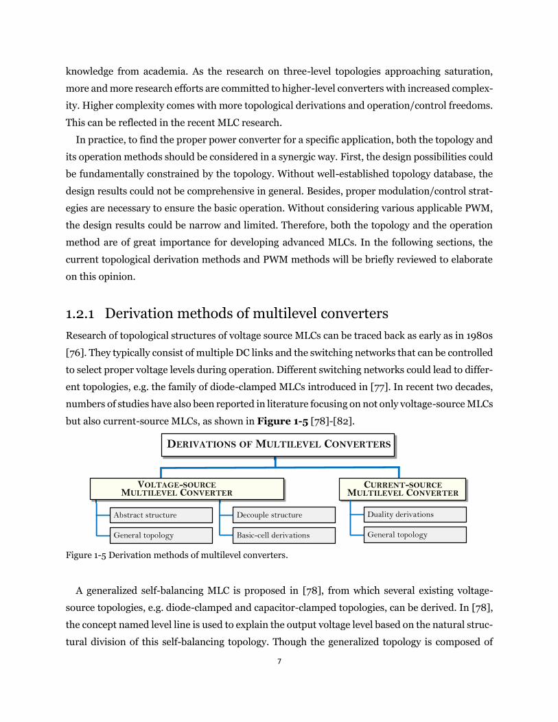
but also current-source MLCs, as shown in Figure 1-5 [78]-[82].
Abstract structure
CURRENT-SOURCE MULTILEVEL CONVERTER
DERIVATIONS OF MULTILEVEL CONVERTERS
General topology
Duality derivations
General topology
Decouple structure
Basic-cell derivations
VOLTAGE-SOURCE MULTILEVEL CONVERTER
Figure 1-5 Derivation methods of multilevel converters.
A generalized self-balancing MLC is proposed in [78], from which several existing voltage-
source topologies, e.g. diode-clamped and capacitor-clamped topologies, can be derived. In [78],
the concept named level line is used to explain the output voltage level based on the natural struc-
tural division of this self-balancing topology. Though the generalized topology is composed of
8
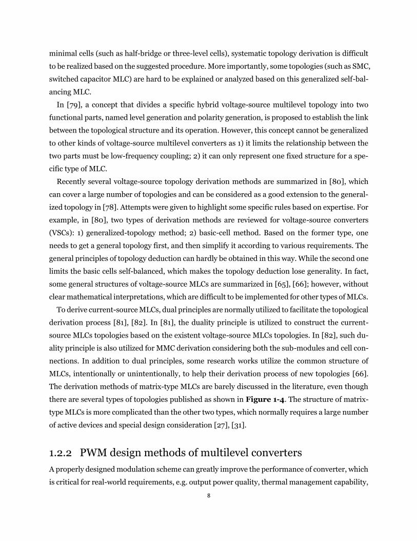
minimal cells (such as half-bridge or three-level cells), systematic topology derivation is difficult
to be realized based on the suggested procedure. More importantly, some topologies (such as SMC,
switched capacitor MLC) are hard to be explained or analyzed based on this generalized self-bal-
ancing MLC.
In [79], a concept that divides a specific hybrid voltage-source multilevel topology into two
functional parts, named level generation and polarity generation, is proposed to establish the link
between the topological structure and its operation. However, this concept cannot be generalized
to other kinds of voltage-source multilevel converters as 1) it limits the relationship between the
two parts must be low-frequency coupling; 2) it can only represent one fixed structure for a spe-
cific type of MLC.
Recently several voltage-source topology derivation methods are summarized in [80], which
can cover a large number of topologies and can be considered as a good extension to the general-
ized topology in [78]. Attempts were given to highlight some specific rules based on expertise. For
example, in [80], two types of derivation methods are reviewed for voltage-source converters
(VSCs): 1) generalized-topology method; 2) basic-cell method. Based on the former type, one
needs to get a general topology first, and then simplify it according to various requirements. The
general principles of topology deduction can hardly be obtained in this way. While the second one
limits the basic cells self-balanced, which makes the topology deduction lose generality. In fact,
some general structures of voltage-source MLCs are summarized in [65], [66]; however, without
clear mathematical interpretations, which are difficult to be implemented for other types of MLCs.
To derive current-source MLCs, dual principles are normally utilized to facilitate the topological
derivation process [81], [82]. In [81], the duality principle is utilized to construct the current-
source MLCs topologies based on the existent voltage-source MLCs topologies. In [82], such du-
ality principle is also utilized for MMC derivation considering both the sub-modules and cell con-
nections. In addition to dual principles, some research works utilize the common structure of
MLCs, intentionally or unintentionally, to help their derivation process of new topologies [66].
The derivation methods of matrix-type MLCs are barely discussed in the literature, even though
there are several types of topologies published as shown in Figure 1-4. The structure of matrix-
type MLCs is more complicated than the other two types, which normally requires a large number
of active devices and special design consideration [27], [31].
1.2.2 PWM design methods of multilevel converters
A properly designed modulation scheme can greatly improve the performance of converter, which
is critical for real-world requirements, e.g. output power quality, thermal management capability,
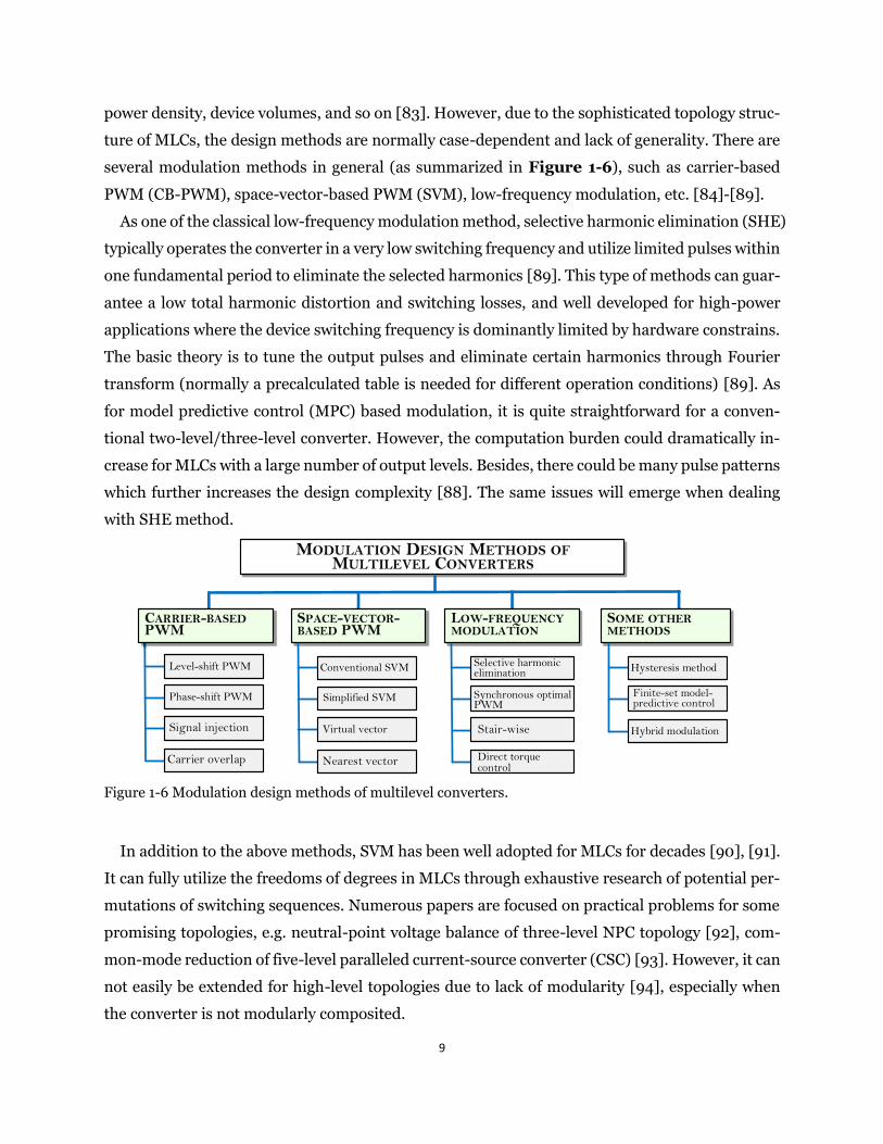
9
power density, device volumes, and so on [83]. However, due to the sophisticated topology struc-
ture of MLCs, the design methods are normally case-dependent and lack of generality. There are
several modulation methods in general (as summarized in Figure 1-6), such as carrier-based
PWM (CB-PWM), space-vector-based PWM (SVM), low-frequency modulation, etc. [84]-[89].
As one of the classical low-frequency modulation method, selective harmonic elimination (SHE)
typically operates the converter in a very low switching frequency and utilize limited pulses within
one fundamental period to eliminate the selected harmonics [89]. This type of methods can guar-
antee a low total harmonic distortion and switching losses, and well developed for high-power
applications where the device switching frequency is dominantly limited by hardware constrains.
The basic theory is to tune the output pulses and eliminate certain harmonics through Fourier
transform (normally a precalculated table is needed for different operation conditions) [89]. As
for model predictive control (MPC) based modulation, it is quite straightforward for a conven-
tional two-level/three-level converter. However, the computation burden could dramatically in-
crease for MLCs with a large number of output levels. Besides, there could be many pulse patterns
which further increases the design complexity [88]. The same issues will emerge when dealing
with SHE method.
Level-shift PWM
MODULATION DESIGN METHODS OF MULTILEVEL CONVERTERS
CARRIER-BASED PWM
SPACE-VECTOR-BASED PWM
LOW-FREQUENCY MODULATION
SOME OTHER METHODS
Signal injection
Carrier overlap
Phase-shift PWM Simplified SVM
Nearest vector
Virtual vector
Conventional SVM
Stair-wise
Direct torque control
Selective harmonic elimination
Synchronous optimal PWM
Hysteresis method
Finite-set model-predictive control
Hybrid modulation
Figure 1-6 Modulation design methods of multilevel converters.
In addition to the above methods, SVM has been well adopted for MLCs for decades [90], [91].
It can fully utilize the freedoms of degrees in MLCs through exhaustive research of potential per-
mutations of switching sequences. Numerous papers are focused on practical problems for some
promising topologies, e.g. neutral-point voltage balance of three-level NPC topology [92], com-
mon-mode reduction of five-level paralleled current-source converter (CSC) [93]. However, it can
not easily be extended for high-level topologies due to lack of modularity [94], especially when
the converter is not modularly composited.
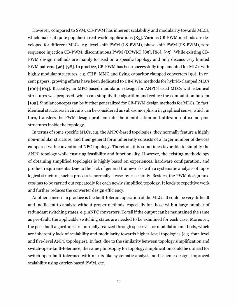
10
However, compared to SVM, CB-PWM has inherent scalability and modularity towards MLCs,
which makes it quite popular in real-world applications [85]. Various CB-PWM methods are de-
veloped for different MLCs, e.g. level shift PWM (LS-PWM), phase shift PWM (PS-PWM), zero
sequence injection CB-PWM, discontinuous PWM (DPWM) [85], [86], [95]. While existing CB-
PWM design methods are mainly focused on a specific topology and only discuss very limited
PWM patterns [96]-[98]. In practice, CB-PWM has been successfully implemented for MLCs with
highly modular structures, e.g. CHB, MMC and flying-capacitor clamped converters [99]. In re-
cent papers, growing efforts have been dedicated to CB-PWM methods for hybrid-clamped MLCs
[100]-[104]. Recently, an MPC-based modulation design for ANPC-based MLCs with identical
structures was proposed, which can simplify the algorithm and reduce the computation burden
[105]. Similar concepts can be further generalized for CB-PWM design methods for MLCs. In fact,
identical structures in circuits can be considered as sub-isomorphism in graphical sense, which in
turn, transfers the PWM design problem into the identification and utilization of isomorphic
structures inside the topology.
In terms of some specific MLCs, e.g. the ANPC-based topologies, they normally feature a highly
non-modular structure, and their general form inherently consists of a larger number of devices
compared with conventional NPC topology. Therefore, it is sometimes favorable to simplify the
ANPC topology while ensuring feasibility and functionality. However, the existing methodology
of obtaining simplified topologies is highly based on experiences, hardware configuration, and
product requirements. Due to the lack of general frameworks with a systematic analysis of topo-
logical structure, such a process is normally a case-by-case study. Besides, the PWM design pro-
cess has to be carried out repeatedly for each newly simplified topology. It leads to repetitive work
and further reduces the converter design efficiency.
Another concern in practice is the fault-tolerant operation of the MLCs. It could be very difficult
and inefficient to analyze without proper methods, especially for those with a large number of
redundant switching states, e.g. ANPC converters. To tell if the output can be maintained the same
as pre-fault, the applicable switching states are needed to be examined for each case. Moreover,
the post-fault algorithms are normally realized through space-vector modulation methods, which
are inherently lack of scalability and modularity towards higher-level topologies (e.g. four-level
and five-level ANPC topologies). In fact, due to the similarity between topology simplification and
switch-open-fault-tolerance, the same philosophy for topology simplification could be utilized for
switch-open-fault-tolerance with merits like systematic analysis and scheme design, improved
scalability using carrier-based PWM, etc.
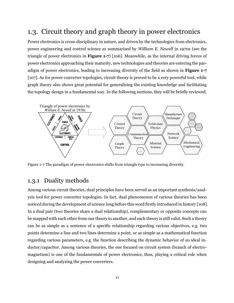
11
1.3. Circuit theory and graph theory in power electronics
Power electronics is cross-disciplinary in nature, and driven by the technologies from electronics,
power engineering and control science as summarized by William E. Newell in 1970s (see the
triangle of power electronics in Figure 1-7) [106]. Meanwhile, as the internal driving forces of
power electronics approaching their maturity, new technologies and theories are entering the par-
adigm of power electronics, leading to increasing diversity of the field as shown in Figure 1-7
[107]. As for power converter topologies, circuit theory is proved to be a very powerful tool, while
graph theory also shows great potential for generalizing the existing knowledge and facilitating
the topology design in a fundamental way. In the following sections, they will be briefly reviewed.
Triangle of power electronics by William E. Newell in 1970s
Figure 1-7 The paradigm of power electronics shifts from triangle type to increasing diversity.
1.3.1 Duality methods
Among various circuit theories, dual principles have been served as an important synthesis/anal-
ysis tool for power converter topologies. In fact, dual phenomenon of various theories has been
noticed during the development of science long before this word firstly introduced in history [108].
In a dual pair (two theories share a dual relationship), complementary or opposite concepts can
be mapped with each other from one theory to another, and each theory is still valid. Such a theory
can be as simple as a sentence of a specific relationship regarding various objectives, e.g. two
points determine a line and two lines determine a point, or as simple as a mathematical function
regarding various parameters, e.g. the function describing the dynamic behavior of an ideal in-
ductor/capacitor. Among various theories, the one focused on circuit system (branch of electro-
magnetism) is one of the fundamentals of power electronics, thus, playing a critical role when
designing and analyzing the power converters.
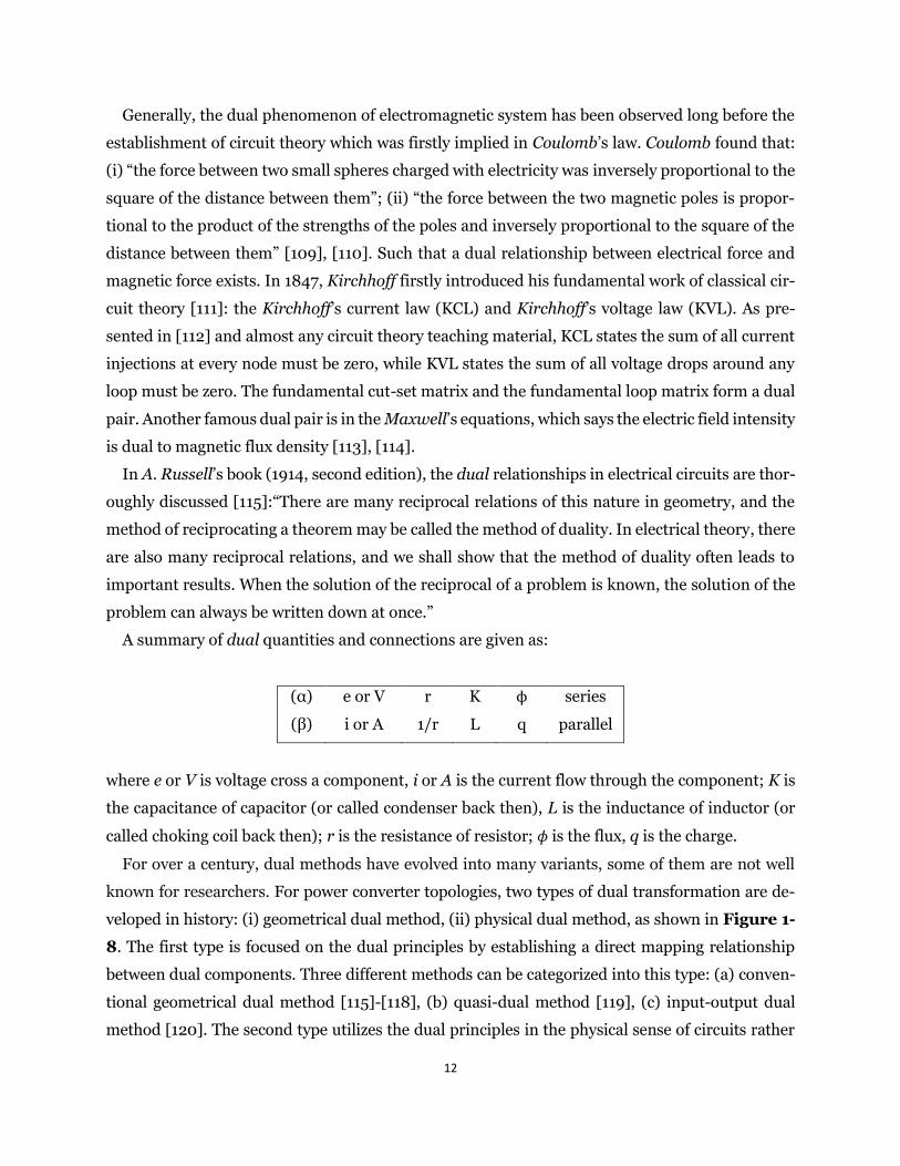
12
Generally, the dual phenomenon of electromagnetic system has been observed long before the
establishment of circuit theory which was firstly implied in Coulomb’s law. Coulomb found that:
(i) “the force between two small spheres charged with electricity was inversely proportional to the
square of the distance between them”; (ii) “the force between the two magnetic poles is propor-
tional to the product of the strengths of the poles and inversely proportional to the square of the
distance between them” [109], [110]. Such that a dual relationship between electrical force and
magnetic force exists. In 1847, Kirchhoff firstly introduced his fundamental work of classical cir-
cuit theory [111]: the Kirchhoff’s current law (KCL) and Kirchhoff’s voltage law (KVL). As pre-
sented in [112] and almost any circuit theory teaching material, KCL states the sum of all current
injections at every node must be zero, while KVL states the sum of all voltage drops around any
loop must be zero. The fundamental cut-set matrix and the fundamental loop matrix form a dual
pair. Another famous dual pair is in the Maxwell’s equations, which says the electric field intensity
is dual to magnetic flux density [113], [114].
In A. Russell’s book (1914, second edition), the dual relationships in electrical circuits are thor-
oughly discussed [115]:“There are many reciprocal relations of this nature in geometry, and the
method of reciprocating a theorem may be called the method of duality. In electrical theory, there
are also many reciprocal relations, and we shall show that the method of duality often leads to
important results. When the solution of the reciprocal of a problem is known, the solution of the
problem can always be written down at once.”
A summary of dual quantities and connections are given as:
(α) e or V r K ϕ series
(β) i or A 1/r L q parallel
where e or V is voltage cross a component, i or A is the current flow through the component; K is
the capacitance of capacitor (or called condenser back then), L is the inductance of inductor (or
called choking coil back then); r is the resistance of resistor; ϕ is the flux, q is the charge.
For over a century, dual methods have evolved into many variants, some of them are not well
known for researchers. For power converter topologies, two types of dual transformation are de-
veloped in history: (i) geometrical dual method, (ii) physical dual method, as shown in Figure 1-
8. The first type is focused on the dual principles by establishing a direct mapping relationship
between dual components. Three different methods can be categorized into this type: (a) conven-
tional geometrical dual method [115]-[118], (b) quasi-dual method [119], (c) input-output dual
method [120]. The second type utilizes the dual principles in the physical sense of circuits rather
13
than topological structure, thus, normally based on the equivalent transformation of circuit dy-
namics [121].
Figure 1-8 Milestones of duality theory for electrical circuit and power converter.
1.3.2 Graphical methods
The graph theory can be dated back to 1736 when Euler dealt with the famous puzzle of the bridges
of Königsberg [122]. Since then, it has been evolved into an important mathematical tool and
found significant applications in various applications [123], e.g. Chemistry, Physics, Biology,
Computer science, etc. Here the special focus is given on the graph theory for electrical engineer-
ing. Many concepts and tools from graph theory have been introduced in this area, e.g. trees, pla-
nar graph, directed graph, adjacency matrix, etc. Until recently, dedicated works keep emerging
in power system/electronics utilizing graph theoretical methods [124]-[128].
Among various concepts in graph theory, isomorphism of graphs is one of the most important
concepts but hardly be mentioned in power electronics. In fact, the definition of isomorphic graph
was systematically presented in the graph-theoretical field till the early 1930s [129]. A similar
word homeomorphism (coined by Poincaré in 1895) appeared in literature quite earlier and its
concept kept evolving till 1930s [130]. There is another confusing concept homomorphism in the
graph theory, which can be thought as a more general graphical mapping than isomorphism [131].
In power electronics field, isomorphism or homomorphism is normally replaced by a much more
ambiguous word “equivalence” to state a similarity between two circuits (geometrically or
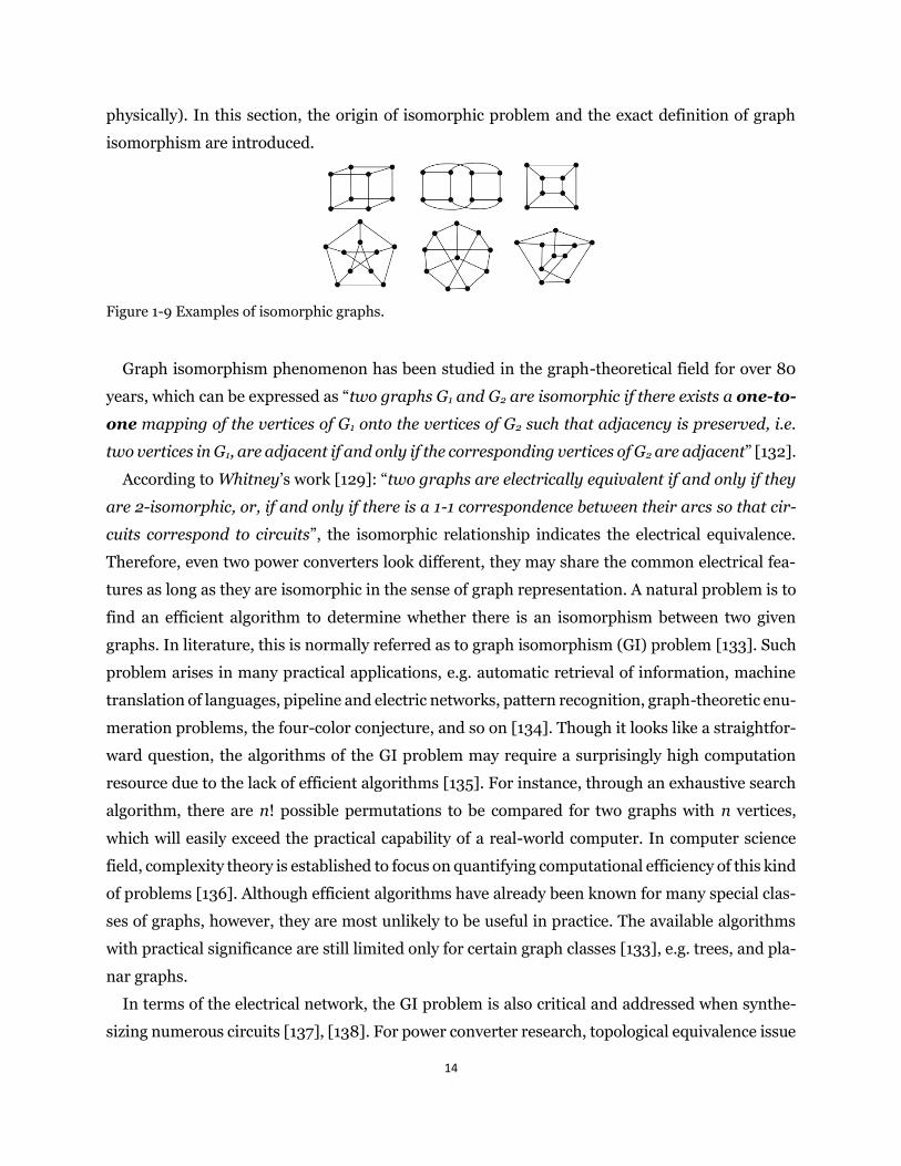
14
physically). In this section, the origin of isomorphic problem and the exact definition of graph
isomorphism are introduced.
Figure 1-9 Examples of isomorphic graphs.
Graph isomorphism phenomenon has been studied in the graph-theoretical field for over 80
years, which can be expressed as “two graphs G1 and G2 are isomorphic if there exists a one-to-
one mapping of the vertices of G1 onto the vertices of G2 such that adjacency is preserved, i.e.
two vertices in G1, are adjacent if and only if the corresponding vertices of G2 are adjacent” [132].
According to Whitney’s work [129]: “two graphs are electrically equivalent if and only if they
are 2-isomorphic, or, if and only if there is a 1-1 correspondence between their arcs so that cir-
cuits correspond to circuits”, the isomorphic relationship indicates the electrical equivalence.
Therefore, even two power converters look different, they may share the common electrical fea-
tures as long as they are isomorphic in the sense of graph representation. A natural problem is to
find an efficient algorithm to determine whether there is an isomorphism between two given
graphs. In literature, this is normally referred as to graph isomorphism (GI) problem [133]. Such
problem arises in many practical applications, e.g. automatic retrieval of information, machine
translation of languages, pipeline and electric networks, pattern recognition, graph-theoretic enu-
meration problems, the four-color conjecture, and so on [134]. Though it looks like a straightfor-
ward question, the algorithms of the GI problem may require a surprisingly high computation
resource due to the lack of efficient algorithms [135]. For instance, through an exhaustive search
algorithm, there are n! possible permutations to be compared for two graphs with n vertices,
which will easily exceed the practical capability of a real-world computer. In computer science
field, complexity theory is established to focus on quantifying computational efficiency of this kind
of problems [136]. Although efficient algorithms have already been known for many special clas-
ses of graphs, however, they are most unlikely to be useful in practice. The available algorithms
with practical significance are still limited only for certain graph classes [133], e.g. trees, and pla-
nar graphs.
In terms of the electrical network, the GI problem is also critical and addressed when synthe-
sizing numerous circuits [137], [138]. For power converter research, topological equivalence issue
15
of DC-DC converters with three switches (it is actually GI problem) was highlighted in [139], and
dealt with by specific algorithms. The complexity of such equivalence could dramatically increase
as the circuits of MLCs consisting of more nodes and branches. In fact, the GI phenomenon can
be found not only in the same type of converters (DC-DC converters), but also in different types
of converters, e.g. direct matrix converter (AC-AC) and the T-type NPC converter (DC-AC or AC-
DC) have the same structure as revealed in [20]. Benefit from the structural equivalence, unified
modulations were proposed for direct matrix converter using the carrier-based concept for T-type
NPC converter. Therefore, the existing knowledge of well-known topologies (e.g. T-type NPC con-
verter) can be transformed into the associated topologies (direct matrix converter), which could
potentially facilitate the analysis and design process. However, up to now, the fundamental rela-
tionships among different MLCs are still unclear. This indeed inspires us to re-consider the rela-
tionships of various types of MLCs in graph theoretical perspectives, especially for some VSCs and
CSCs with unfamiliar topologies.
1.3.3 Topology cycling phenomenon
The duality and isomorphism are some common features in the science of nature. However, dif-
ferent interpretations in various disciplines make the concept even more inexplicit and mysteri-
ous. In fact, both duality and isomorphism have their mathematical interpretation in category
theory. The category theory was formulated originally for abstract algebra fields in 1945 by Eilen-
berg and Mac Lane. Then, its applications widely appeared in computer science, linguistics, cog-
nitive science, philosophy, and many other areas [140], [141]. From a categorical perspective, if
duality and isomorphism are bijective transformations, then, a topology can be transformed into
itself by limited steps of dual/isomorphic bijections. In fact, this indicates a cycling phenomenon
in power converters, and not only the circuit, but also the features can be shared with various
topologies in theory.
In literature, such a phenomenon has gained some early attention. In 1979, S. Cuk discussed
the DC-DC converter and found that after the dual transformation of the Cuk converter, the de-
rived topology had the same circuit as the original one [142]. He defined such feature as topolog-
ical “invariant”. In 2014, B. W. Williams stated following the discovery in [143]: “This repeated
reversing and flip processing of a viable topology will always give a sequence of cycling viable
topologies and will cycle back to the original topology.” In [143], duality and unique circuit recon-
figuration rules (e.g. flip, inverse) are used to derive DC-DC converters. Since the inverse process
does not change the graph of power converter, but only interchanges the inputs and outputs, the
resulting converters can be considered as graph isomorphism. The phenomenon was also
16
appeared in a recent paper, e.g. DC-DC converter synthesis method in 2020 [144]. Though widely
exists, unfortunately, neither the theoretical nor the practical investigations of this cycling phe-
nomenon for power converters have been available in the existing literature.
As the database of topologies expanding fast, resemble circuits and methods are needed to be
recognized systematically, so that, wasted repetitive research efforts can be avoided. To achieve
such a goal, the fundamental relationships among various power converters topologies should be
defined clearly to link different converters with universal principles. This is ultimately important
for MLCs, since they tend to have complicated circuits and normally are involved in great design
efforts. The duality from circuit theory has been proved to be very successful when dealing with
power converters. Meanwhile, the isomorphism from graph theory also shows some great poten-
tial that can be implemented. Furthermore, they can also be used to transfer the existing
knowledge of some existing topologies and facilitate the design process in a more general way. On
top of that, though the topology cycling phenomenon can be deduced in category theory and has
gained some rough thoughts in literature, its fundamentals are still unclear. In this work, it will
be investigated and implemented for power converter, in particular, the VSCs and CSCs for the
first time through the well-established dual principles and emerging isomorphic theory.
1.4. Research objectives and contributions
The increased diversity of research paradigm along with emerging applications, e.g. low voltage
applications, drives the MLC technique towards their mature stage with higher performance in
general, which requiring innovated design methodology. Since the scaling laws of low voltage
fields could be different from conventional medium/high voltage scenarios, more MLCs topolo-
gies could be accepted as reasonable candidates. As briefly reviewed before, the current topol-
ogy/modulation methods are mainly utilized in a case-by-case or type-by-type way. This may nar-
row down the power converter design space and lead to sub-optimal results when finding a proper
converter and its suitable operation method. To avoid such limitations, systematic topological
synthesis and modulation design methods are necessary to improve the design database of MLC
topologies with more derivatives and increased circuit-level complexity.
In detail, there are several research objectives and contributions to this work:
(1) Topology fundamental relationships of power converters
With increasing new power topologies, a large number of circuits with resembling structures
and similar features could emerge and such phenomenon could be more extensive in the future.
This may lead to wasted research resources when similar circuits/schemes are being rein-
vented/re-examined. Therefore, it is beneficial to establish the well-defined, clear and universal
17
relationships among various power converter topologies, such that the existing and future derived
topologies can be linked with each other and sharing the existing knowledge in a more compre-
hensive way. In Chapter 2, the universal relationships for power converters, especially the VSCs
and CSCs, will be investigated based on the dual theory and the graphical isomorphic theory. Fur-
thermore, by synergistically implementation of these two theories, the topology cycling phenom-
enon will be discussed for different kinds of VSCs and CSCs. With such relationships, the derived
topology or PWM can also be utilized for other topology, therefore, further reduce the design bur-
den and accelerate the design process.
(2) Mathematical model and general derivation rules for MLCs
The derivation methods for voltage-source MLCs have been developed for nearly 50 years, how-
ever, the current approaches are still highly dependent on the expertise of designers and cannot
cover all the main types of topologies. Meanwhile, as important types of MLCs, the current-source
type and the matrix-based type have not been well studied. From the circuit level, both the math-
ematical unifications and the general derivation rules of different MLCs are still unclear. This
indeed highly limits the understanding of various MLCs, and potentially leads to narrow and bi-
ased designs. To deal with such issue, unified mathematical models of MLCs should be obtained
by establishing the fundamental relationships among different topologies in a structure-level. And
then, the general derivation rules can be introduced to concretely deal with the MLC derivation
issues in a comprehensive way. This part of work will be discussed in detail in Chapter 3.
(3) PWM design for non-modular MLC topology
Suffering from a more complex circuit appearance, the PWM design of some non-modular
MLCs tend to become dramatically complicated with an increased number of output levels. Till
present, the general PWM design method is still missing for those with complicated circuits and
lack of modular structure. In particular, ANPC converters are chosen as examples since most of
the non-modular MLCs can be derived from this type. To fully explore the potentials of MLCs,
especially for the internal device utilizations, the new modulation design method is highly de-
manding and will be presented in Chapter 4. On the other hand, the multilevel ANPC converters
have more control freedoms compared to the conventional NPC topology due to increased switch-
ing redundancies. However, the device utilization is inherently low with conventional PWM meth-
ods compare to other modular MLCs (e.g. FCC, CHB converters and MMC). To deal with such
challenge, the identical circuits in ANPC topology are utilized in Chapter 4 with PS PWM method
to achieve similar features in CHB converter or MMC.
(4) Practical concerns in terms of converter simplifications and fault-tolerance
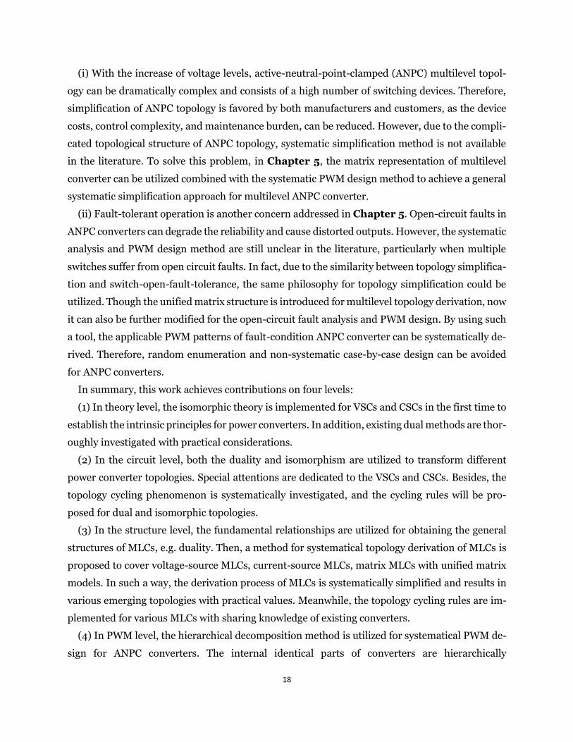
18
(i) With the increase of voltage levels, active-neutral-point-clamped (ANPC) multilevel topol-
ogy can be dramatically complex and consists of a high number of switching devices. Therefore,
simplification of ANPC topology is favored by both manufacturers and customers, as the device
costs, control complexity, and maintenance burden, can be reduced. However, due to the compli-
cated topological structure of ANPC topology, systematic simplification method is not available
in the literature. To solve this problem, in Chapter 5, the matrix representation of multilevel
converter can be utilized combined with the systematic PWM design method to achieve a general
systematic simplification approach for multilevel ANPC converter.
(ii) Fault-tolerant operation is another concern addressed in Chapter 5. Open-circuit faults in
ANPC converters can degrade the reliability and cause distorted outputs. However, the systematic
analysis and PWM design method are still unclear in the literature, particularly when multiple
switches suffer from open circuit faults. In fact, due to the similarity between topology simplifica-
tion and switch-open-fault-tolerance, the same philosophy for topology simplification could be
utilized. Though the unified matrix structure is introduced for multilevel topology derivation, now
it can also be further modified for the open-circuit fault analysis and PWM design. By using such
a tool, the applicable PWM patterns of fault-condition ANPC converter can be systematically de-
rived. Therefore, random enumeration and non-systematic case-by-case design can be avoided
for ANPC converters.
In summary, this work achieves contributions on four levels:
(1) In theory level, the isomorphic theory is implemented for VSCs and CSCs in the first time to
establish the intrinsic principles for power converters. In addition, existing dual methods are thor-
oughly investigated with practical considerations.
(2) In the circuit level, both the duality and isomorphism are utilized to transform different
power converter topologies. Special attentions are dedicated to the VSCs and CSCs. Besides, the
topology cycling phenomenon is systematically investigated, and the cycling rules will be pro-
posed for dual and isomorphic topologies.
(3) In the structure level, the fundamental relationships are utilized for obtaining the general
structures of MLCs, e.g. duality. Then, a method for systematical topology derivation of MLCs is
proposed to cover voltage-source MLCs, current-source MLCs, matrix MLCs with unified matrix
models. In such a way, the derivation process of MLCs is systematically simplified and results in
various emerging topologies with practical values. Meanwhile, the topology cycling rules are im-
plemented for various MLCs with sharing knowledge of existing converters.
(4) In PWM level, the hierarchical decomposition method is utilized for systematical PWM de-
sign for ANPC converters. The internal identical parts of converters are hierarchically
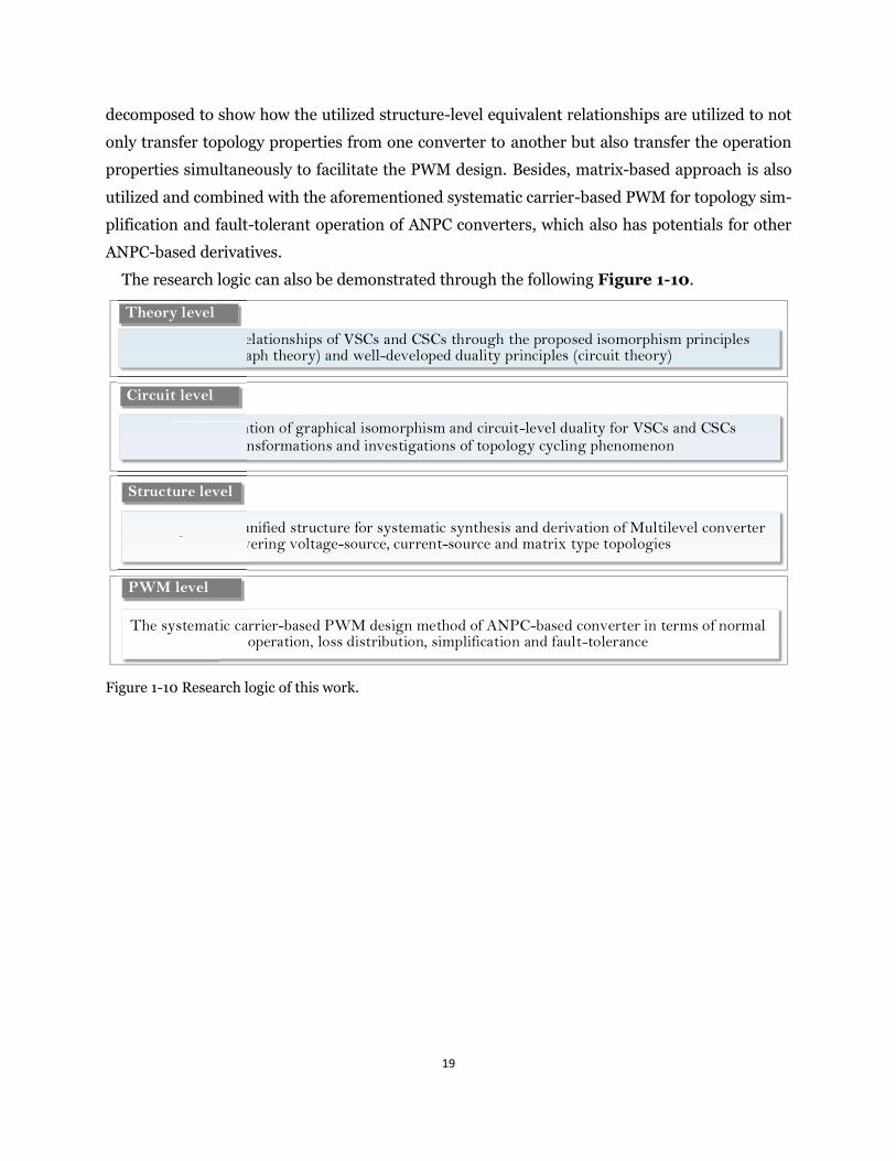
19
decomposed to show how the utilized structure-level equivalent relationships are utilized to not
only transfer topology properties from one converter to another but also transfer the operation
properties simultaneously to facilitate the PWM design. Besides, matrix-based approach is also
utilized and combined with the aforementioned systematic carrier-based PWM for topology sim-
plification and fault-tolerant operation of ANPC converters, which also has potentials for other
ANPC-based derivatives.
The research logic can also be demonstrated through the following Figure 1-10.
Fundamental relationships of VSCs and CSCs through the proposed isomorphism principles (graph theory) and well-developed duality principles (circuit theory)
Implementation of graphical isomorphism and circuit-level duality for VSCs and CSCs transformations and investigations of topology cycling phenomenon
The systematic carrier-based PWM design method of ANPC-based converter in terms of normal operation, loss distribution, simplification and fault-tolerance
Development of unified structure for systematic synthesis and derivation of Multilevel converter covering voltage-source, current-source and matrix type topologies
Fundamental relationships of (graph theory)
Implementation of graphical isomorphism and circuittransformations and investigations of topology cycling phenomenon
Development of unified structure for systematic synthesis and derivation of Multilevel converter covering
Theory level
Circuit level
Structure level
PWM level
Figure 1-10 Research logic of this work.
20
Chapter 2 Fundamental relationships of power
converters1
As briefly reviewed in Chapter 1, the topology derivation and modulation design are two of the
challenges in MLC research, and lack of systematic methodologies. This can be potentially solved
by developing new fundamental relationships among power converters. Historically, various to-
pologies were developed through topological transformation in a circuit/graph theoretical per-
spective. To better understand the relationship of various converter topologies, circuit theory
combined with graph theory can be utilized to link different circuits with universal principles.
In this chapter, the major achievements are focused on the theoretical level innovations of the
power converters, in particular, for VSCs and CSCs. In details, three tasks have been done: (1)
First, the dual transformation of power converters is thoroughly demonstrated, some of them may
not be well-known by the power electronics community, i.e. duality in non-planar circuits; (2)
Furthermore, the isomorphic transformation is investigated for VSCs and CSCs in the first time,
followed by its potentials on modulation design; (3) At the end, the cycling phenomenon of dual
and isomorphic converters is elaborated for the first time. Cycling rules are highlighted with dis-
cussions of potential applications.
These achievements can facilitate topology derivation and modulation design in comprehensive
ways. For instance, the isomorphic theory can be utilized to transfer the existing modulation
schemes from one converter to its isomorphic converter. Such isomorphism can be utilized to
unify the modulation design process, providing a much more systematic approach covering vari-
ous VSCs and CSCs. In Chapter 3, the relationships in a structure level of the MLCs are investi-
gated, e.g. duality, resulting in the unified matrix models of the MLCs that will be utilized for
1 Publications out of this Chapter:
Yuzhuo Li and Yunwei Li, "Power Converters Topological Transformation Using Dual and Isomorphic Principles," in IEEE Open Journal of Power Electronics, vol. 1, pp. 74-87, 2020. Yuzhuo Li, Li Ding and Yunwei Li, "Isomorphic Relationships between Voltage-Source and Current-Source Converters," in IEEE Transactions on Power Electronics, vol. 34, no. 8, pp. 7131-7135, Aug. 2019. Yuzhuo Li and Yunwei Li, "Dual and Isomorphic Power Converters with the Topology Cycling Phenomenon," 2020 IEEE Applied Power Electronics Conference and Exposition (APEC), New Orleans, LA, USA, 2020, pp. 1176-1182. Li Ding, Yuzhuo Li and Yunwei Li, "A New Current Source Converter Using AC-type Flying-Capacitor Technique," in IEEE Trans-actions on Power Electronics, 2021, in press.
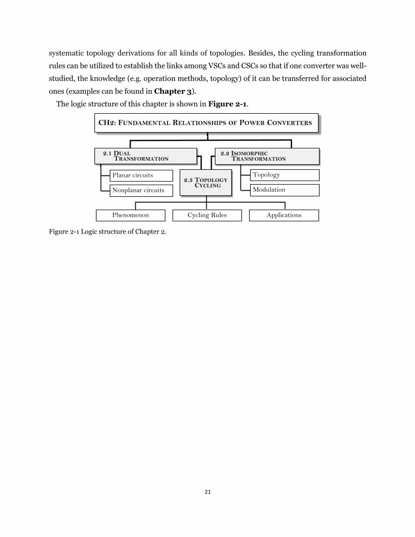
21
systematic topology derivations for all kinds of topologies. Besides, the cycling transformation
rules can be utilized to establish the links among VSCs and CSCs so that if one converter was well-
studied, the knowledge (e.g. operation methods, topology) of it can be transferred for associated
ones (examples can be found in Chapter 3).
The logic structure of this chapter is shown in Figure 2-1.
Planar circuits
2.2 ISOMORPHIC TRANSFORMATION
CH2: FUNDAMENTAL RELATIONSHIPS OF POWER CONVERTERS
Nonplanar circuits
2.1 DUAL TRANSFORMATION
2.3 TOPOLOGY CYCLING
Topology
Modulation
Phenomenon Cycling Rules Applications
Figure 2-1 Logic structure of Chapter 2.
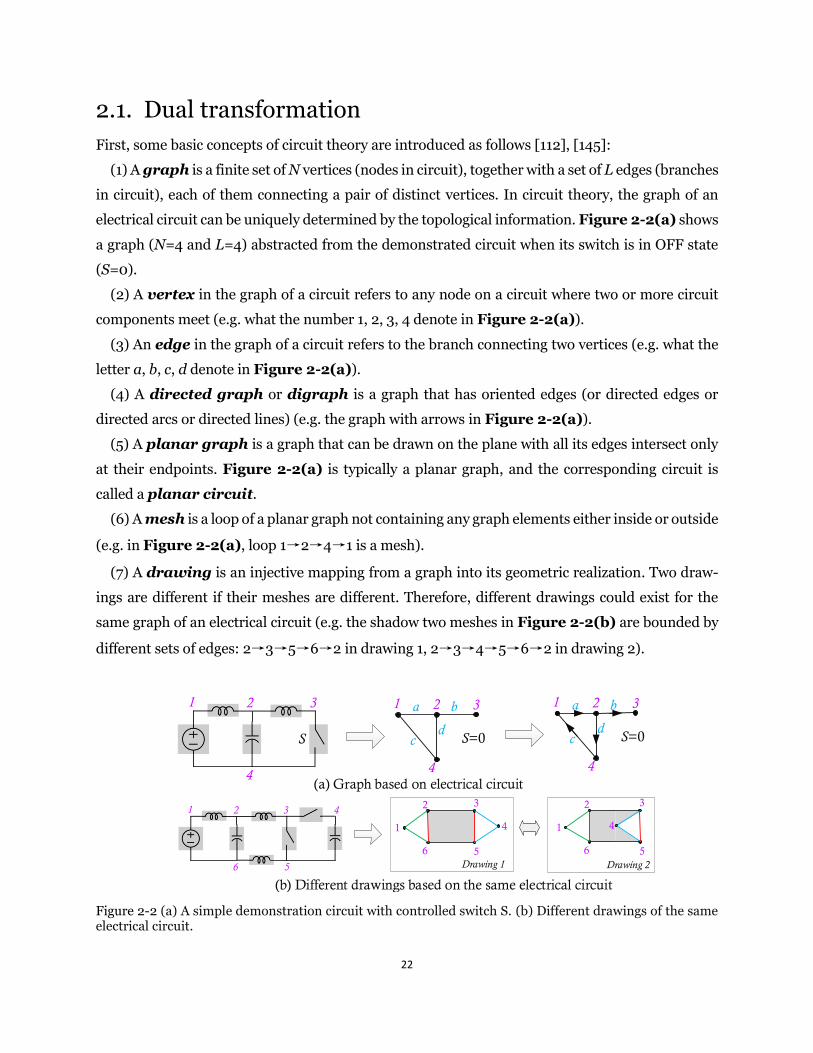
22
2.1. Dual transformation
First, some basic concepts of circuit theory are introduced as follows [112], [145]:
(1) A graph is a finite set of N vertices (nodes in circuit), together with a set of L edges (branches
in circuit), each of them connecting a pair of distinct vertices. In circuit theory, the graph of an
electrical circuit can be uniquely determined by the topological information. Figure 2-2(a) shows
a graph (N=4 and L=4) abstracted from the demonstrated circuit when its switch is in OFF state
(S=0).
(2) A vertex in the graph of a circuit refers to any node on a circuit where two or more circuit
components meet (e.g. what the number 1, 2, 3, 4 denote in Figure 2-2(a)).
(3) An edge in the graph of a circuit refers to the branch connecting two vertices (e.g. what the
letter a, b, c, d denote in Figure 2-2(a)).
(4) A directed graph or digraph is a graph that has oriented edges (or directed edges or
directed arcs or directed lines) (e.g. the graph with arrows in Figure 2-2(a)).
(5) A planar graph is a graph that can be drawn on the plane with all its edges intersect only
at their endpoints. Figure 2-2(a) is typically a planar graph, and the corresponding circuit is
called a planar circuit.
(6) A mesh is a loop of a planar graph not containing any graph elements either inside or outside
(e.g. in Figure 2-2(a), loop 1→2→4→1 is a mesh).
(7) A drawing is an injective mapping from a graph into its geometric realization. Two draw-
ings are different if their meshes are different. Therefore, different drawings could exist for the
same graph of an electrical circuit (e.g. the shadow two meshes in Figure 2-2(b) are bounded by
different sets of edges: 2→3→5→6→2 in drawing 1, 2→3→4→5→6→2 in drawing 2).
2 31
4
S
21 3
4
S=0
a b
cd
21 3
4
S=0
a b
cd
(a) Graph based on electrical circuit2 3
56
1 4
2 3
56
1 4
2 31
6 5
4
(b) Different drawings based on the same electrical circuit
Drawing 1 Drawing 2
Figure 2-2 (a) A simple demonstration circuit with controlled switch S. (b) Different drawings of the same electrical circuit.
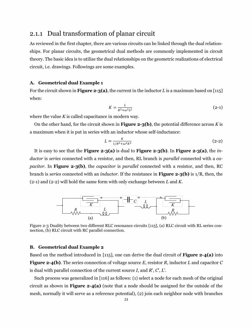
23
2.1.1 Dual transformation of planar circuit
As reviewed in the first chapter, there are various circuits can be linked through the dual relation-
ships. For planar circuits, the geometrical dual methods are commonly implemented in circuit
theory. The basic idea is to utilize the dual relationships on the geometric realizations of electrical
circuit, i.e. drawings. Followings are some examples.
A. Geometrical dual Example 1
For the circuit shown in Figure 2-3(a), the current in the inductor L is a maximum based on [115]
when:
𝐾 =𝐿
𝑅2+𝜔2𝐿2 (2-1)
where the value K is called capacitance in modern way.
On the other hand, for the circuit shown in Figure 2-3(b), the potential difference across K is
a maximum when it is put in series with an inductor whose self-inductance:
𝐿 =𝐾
1/𝑅2+𝜔2𝐾2 (2-2)
It is easy to see that the Figure 2-3(a) is dual to Figure 2-3(b). In Figure 2-3(a), the in-
ductor is series connected with a resistor, and then, RL branch is parallel connected with a ca-
pacitor. In Figure 2-3(b), the capacitor is parallel connected with a resistor, and then, RC
branch is series connected with an inductor. If the resistance in Figure 2-3(b) is 1/R, then, the
(2-1) and (2-2) will hold the same form with only exchange between L and K.
K
R L
L
R
K
(a) (b)
C
Figure 2-3 Duality between two different RLC resonance circuits [115], (a) RLC circuit with RL series con-nection, (b) RLC circuit with RC parallel connection.
B. Geometrical dual Example 2
Based on the method introduced in [115], one can derive the dual circuit of Figure 2-4(a) into
Figure 2-4(b). The series connection of voltage source E, resistor R, inductor L and capacitor C
is dual with parallel connection of the current source I, and R', C', L'.
Such process was generalized in [116] as follows: (1) select a node for each mesh of the original
circuit as shown in Figure 2-4(a) (note that a node should be assigned for the outside of the
mesh, normally it will serve as a reference potential), (2) join each neighbor node with branches
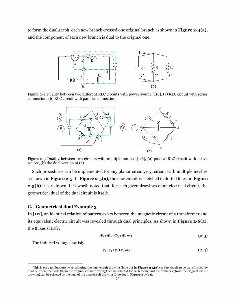
24
to form the dual graph, each new branch crossed one original branch as shown in Figure 2-4(a),
and the component of each new branch is dual to the original one.
C
R
L
(a) (b)
C' R' L'
1
2
3
E
I
1' 2' 3'
ab
Figure 2-4 Duality between two different RLC circuits with power source [116], (a) RLC circuit with series connection, (b) RLC circuit with parallel connection.
(a)
1
E
42 3
5
6 7
1' I
2'
3'
4'
5'
6'
7'
a
bc
e
d
(b)
a
b
c
d
e
Figure 2-5 Duality between two circuits with multiple meshes [116], (a) passive RLC circuit with active source, (b) the dual version of (a).
Such procedures can be implemented for any planar circuit, e.g. circuit with multiple meshes
as shown in Figure 2-5. In Figure 2-5(a), the new circuit is sketched in dotted lines, in Figure
2-5(b) it is redrawn. It is worth noted that, for each given drawings of an electrical circuit, the
geometrical dual of the dual circuit is itself1.
C. Geometrical dual Example 3
In [117], an identical relation of pattern exists between the magnetic circuit of a transformer and
its equivalent electric circuit was revealed through dual principles. As shown in Figure 2-6(a),
the fluxes satisfy:
Φ1+Φ2+Φ3+Φ4=0 (2-3)
The induced voltages satisfy:
e1+e2+e3+e4=0 (2-4)
1 This is easy to illustrate by considering the dual circuit drawing (blue dot in Figure 2-5(a)) as the circuit to be transformed by
duality. Then, the node (from the original circuit drawing) can be selected for each mesh, and the branches (from the original circuit drawing) can be selected as the dual of the dual circuit drawing (blue dot in Figure 2-5(a)).
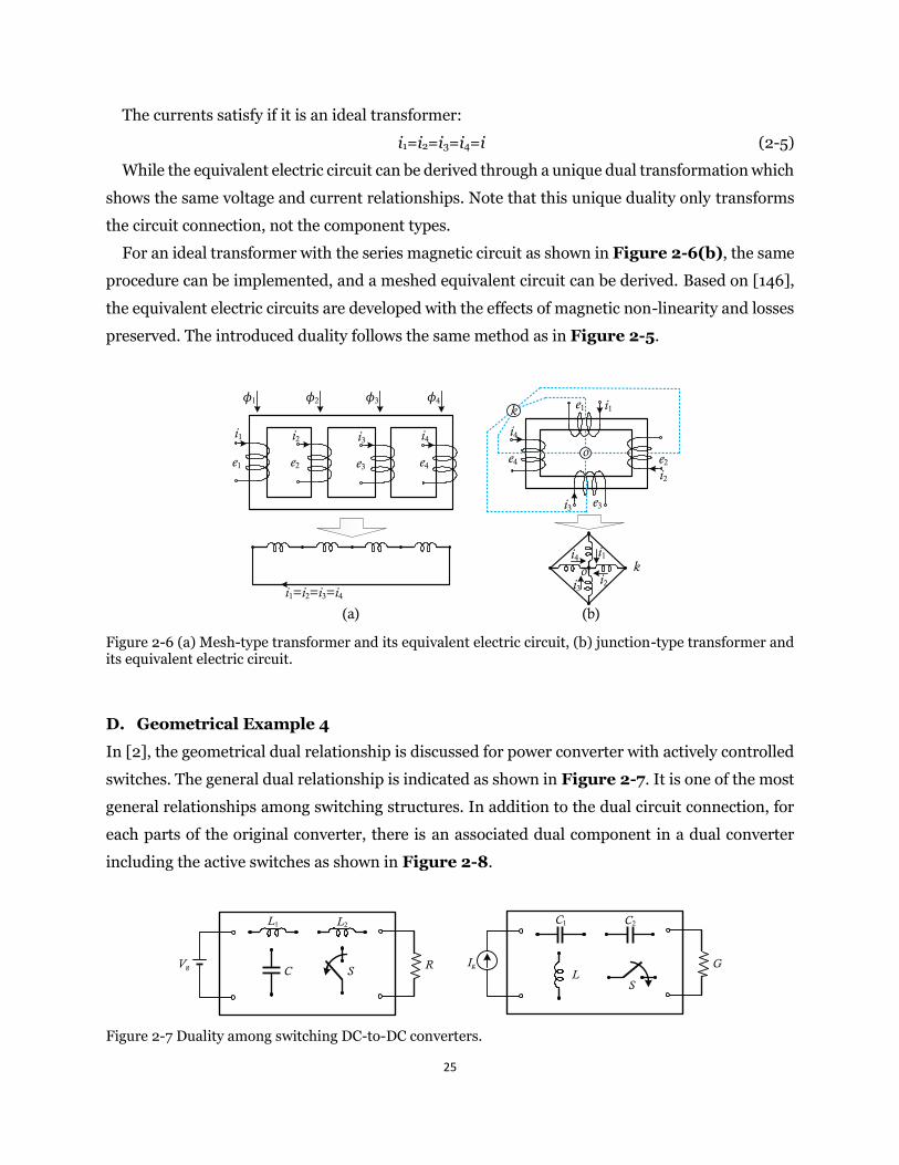
25
The currents satisfy if it is an ideal transformer:
i1=i2=i3=i4=i (2-5)
While the equivalent electric circuit can be derived through a unique dual transformation which
shows the same voltage and current relationships. Note that this unique duality only transforms
the circuit connection, not the component types.
For an ideal transformer with the series magnetic circuit as shown in Figure 2-6(b), the same
procedure can be implemented, and a meshed equivalent circuit can be derived. Based on [146],
the equivalent electric circuits are developed with the effects of magnetic non-linearity and losses
preserved. The introduced duality follows the same method as in Figure 2-5.
(a)
i1
e1
i2
e2
i3
e3
i4
e4
ϕ1 ϕ2 ϕ3 ϕ4
(b)
i1=i2=i3=i4
i4
e4
i1e1
i2
e2
i3 e3
o
k
ko
i1
i2i3
i4
Figure 2-6 (a) Mesh-type transformer and its equivalent electric circuit, (b) junction-type transformer and its equivalent electric circuit.
D. Geometrical Example 4
In [2], the geometrical dual relationship is discussed for power converter with actively controlled
switches. The general dual relationship is indicated as shown in Figure 2-7. It is one of the most
general relationships among switching structures. In addition to the dual circuit connection, for
each parts of the original converter, there is an associated dual component in a dual converter
including the active switches as shown in Figure 2-8.
Vg
L1 L2
C SR Ig
C1 C2
LS
G
Figure 2-7 Duality among switching DC-to-DC converters.
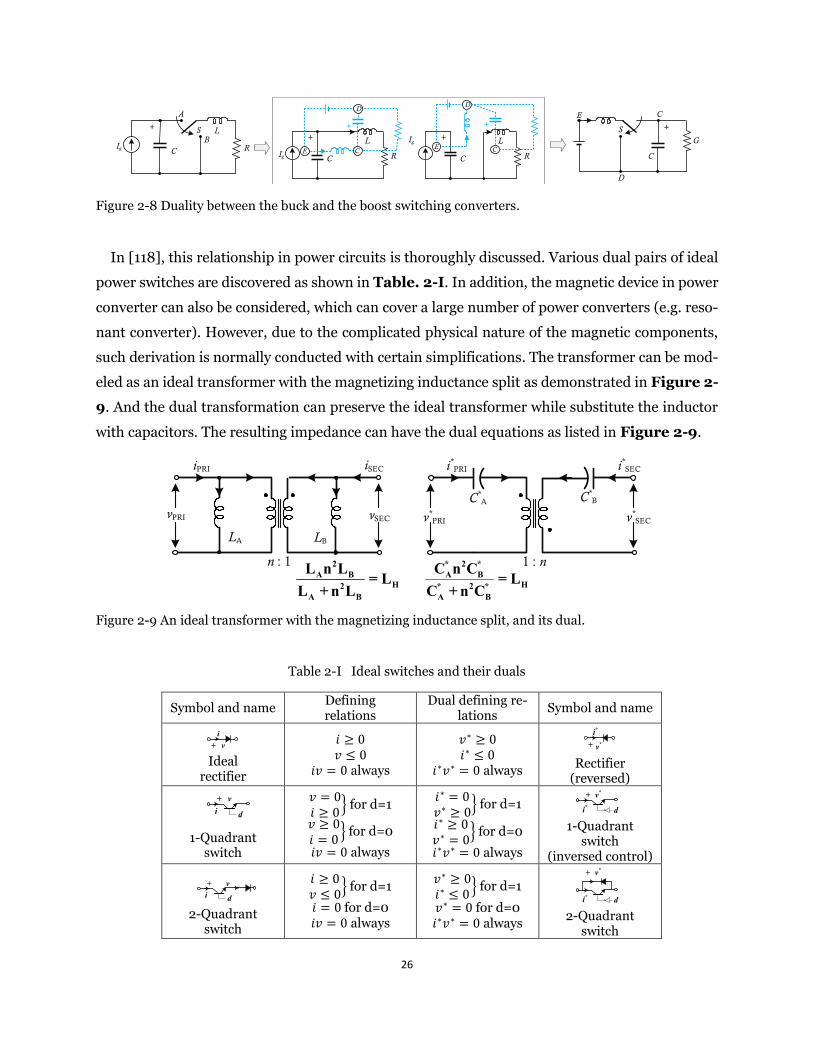
26
Ig C
LS
R
A
B
+
Ig C
L
R
+
Ig
C
L
R
+
C
D
+
D
EE C
+
C
S
G
+
D
E C
Figure 2-8 Duality between the buck and the boost switching converters.
In [118], this relationship in power circuits is thoroughly discussed. Various dual pairs of ideal
power switches are discovered as shown in Table. 2-I. In addition, the magnetic device in power
converter can also be considered, which can cover a large number of power converters (e.g. reso-
nant converter). However, due to the complicated physical nature of the magnetic components,
such derivation is normally conducted with certain simplifications. The transformer can be mod-
eled as an ideal transformer with the magnetizing inductance split as demonstrated in Figure 2-
9. And the dual transformation can preserve the ideal transformer while substitute the inductor
with capacitors. The resulting impedance can have the dual equations as listed in Figure 2-9.
iPRI
n : 1
vPRI vSEC
LA
iSEC
LB
2A B
H2A B
L n L= L
L + n L
i*PRI
1 : n
v*PRI v*
SEC
C*A
i*SEC
C*B
* 2 *A B
H* 2 *A B
C n C= L
C + n C
Figure 2-9 An ideal transformer with the magnetizing inductance split, and its dual.
Table 2-I Ideal switches and their duals
Symbol and name Defining relations
Dual defining re-lations
Symbol and name
iv+
Ideal rectifier
𝑖 ≥ 0 𝑣 ≤ 0
𝑖𝑣 = 0 always
𝑣∗ ≥ 0 𝑖∗ ≤ 0
𝑖∗𝑣∗ = 0 always
i*
v*+
Rectifier (reversed)
d
v+ i
1-Quadrant
switch
𝑣 = 0𝑖 ≥ 0
} for d=1
𝑣 ≥ 0𝑖 = 0
} for d=0
𝑖𝑣 = 0 always
𝑖∗ = 0𝑣∗ ≥ 0
} for d=1
𝑖∗ ≥ 0𝑣∗ = 0
} for d=0
𝑖∗𝑣∗ = 0 always
d
v*+
i*
1-Quadrant
switch (inversed control)
d
v+ i
2-Quadrant
switch
𝑖 ≥ 0𝑣 ≤ 0
} for d=1
𝑖 = 0 for d=0 𝑖𝑣 = 0 always
𝑣∗ ≥ 0𝑖∗ ≤ 0
} for d=1
𝑣∗ = 0 for d=0 𝑖∗𝑣∗ = 0 always
d
v*+
i*
2-Quadrant
switch
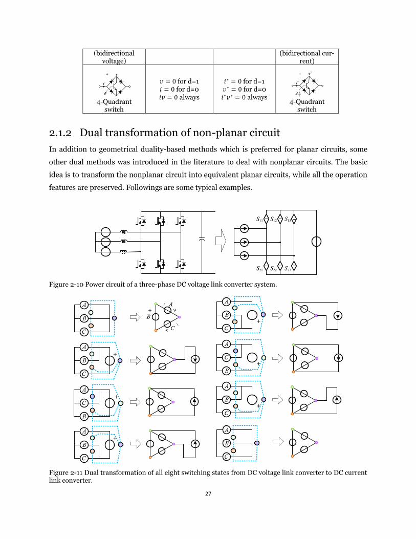
27
(bidirectional voltage)
(bidirectional cur-rent)
d
v+
i
4-Quadrant
switch
𝑣 = 0 for d=1 𝑖 = 0 for d=0 𝑖𝑣 = 0 always
𝑖∗ = 0 for d=1 𝑣∗ = 0 for d=0 𝑖∗𝑣∗ = 0 always
+ v*
i*
d 4-Quadrant
switch
2.1.2 Dual transformation of non-planar circuit
In addition to geometrical duality-based methods which is preferred for planar circuits, some
other dual methods was introduced in the literature to deal with nonplanar circuits. The basic
idea is to transform the nonplanar circuit into equivalent planar circuits, while all the operation
features are preserved. Followings are some typical examples.
S11 S12 S13
S21 S22 S23
Figure 2-10 Power circuit of a three-phase DC voltage link converter system.
A
B
C
A
B
C
A
C
B
A
B
C
A
B
C
+
+
+
+
A
C
B
+
A
B
C
+
A
B
C
A
B
C
+
Figure 2-11 Dual transformation of all eight switching states from DC voltage link converter to DC current link converter.
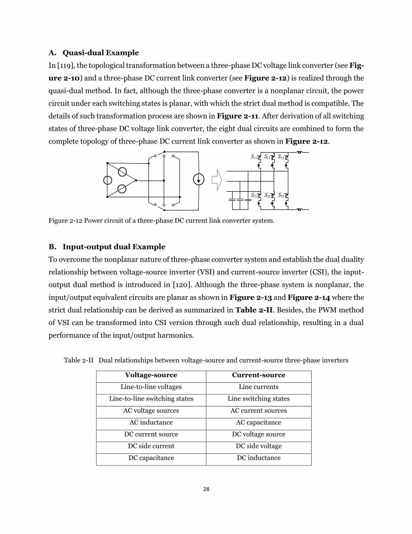
28
A. Quasi-dual Example
In [119], the topological transformation between a three-phase DC voltage link converter (see Fig-
ure 2-10) and a three-phase DC current link converter (see Figure 2-12) is realized through the
quasi-dual method. In fact, although the three-phase converter is a nonplanar circuit, the power
circuit under each switching states is planar, with which the strict dual method is compatible. The
details of such transformation process are shown in Figure 2-11. After derivation of all switching
states of three-phase DC voltage link converter, the eight dual circuits are combined to form the
complete topology of three-phase DC current link converter as shown in Figure 2-12.
S11 S12 S13
S21 S22 S23
Figure 2-12 Power circuit of a three-phase DC current link converter system.
B. Input-output dual Example
To overcome the nonplanar nature of three-phase converter system and establish the dual duality
relationship between voltage-source inverter (VSI) and current-source inverter (CSI), the input-
output dual method is introduced in [120]. Although the three-phase system is nonplanar, the
input/output equivalent circuits are planar as shown in Figure 2-13 and Figure 2-14 where the
strict dual relationship can be derived as summarized in Table 2-II. Besides, the PWM method
of VSI can be transformed into CSI version through such dual relationship, resulting in a dual
performance of the input/output harmonics.
Table 2-II Dual relationships between voltage-source and current-source three-phase inverters
Voltage-source Current-source
Line-to-line voltages Line currents
Line-to-line switching states Line switching states
AC voltage sources AC current sources
AC inductance AC capacitance
DC current source DC voltage source
DC side current DC side voltage
DC capacitance DC inductance
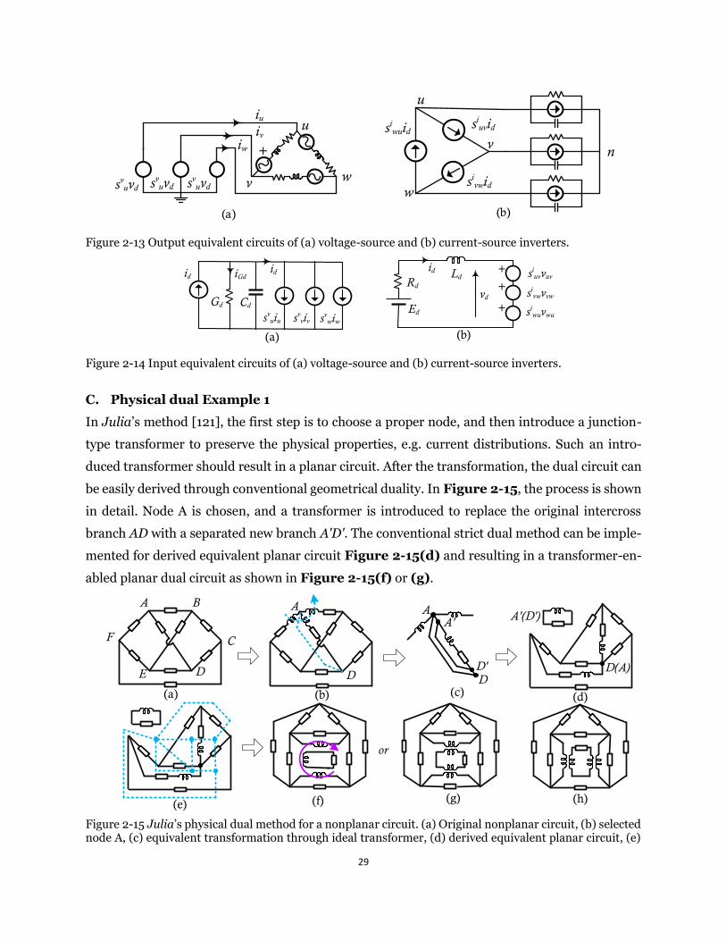
29
u
v
w
siwuid
siuvid
sivwid
n
svuvd sv
uvd svuvd
u
v w
+
iu
iv
iw
(a) (b)
Figure 2-13 Output equivalent circuits of (a) voltage-source and (b) current-source inverters.
id
Gd Cd
iGd
svuiu sv
viv svwiw
id
Rd
id Ld
Ed
+
+
+
siuvvuv
sivwvvw
siwuvwu
vd
(a) (b)
Figure 2-14 Input equivalent circuits of (a) voltage-source and (b) current-source inverters.
C. Physical dual Example 1
In Julia’s method [121], the first step is to choose a proper node, and then introduce a junction-
type transformer to preserve the physical properties, e.g. current distributions. Such an intro-
duced transformer should result in a planar circuit. After the transformation, the dual circuit can
be easily derived through conventional geometrical duality. In Figure 2-15, the process is shown
in detail. Node A is chosen, and a transformer is introduced to replace the original intercross
branch AD with a separated new branch A'D'. The conventional strict dual method can be imple-
mented for derived equivalent planar circuit Figure 2-15(d) and resulting in a transformer-en-
abled planar dual circuit as shown in Figure 2-15(f) or (g).
A B
C
DE
F
A
D
A
DD'
A'
D(A)
A'(D')
or
(a) (b) (c) (d)
(e) (f) (g) (h)
Figure 2-15 Julia’s physical dual method for a nonplanar circuit. (a) Original nonplanar circuit, (b) selected node A, (c) equivalent transformation through ideal transformer, (d) derived equivalent planar circuit, (e)
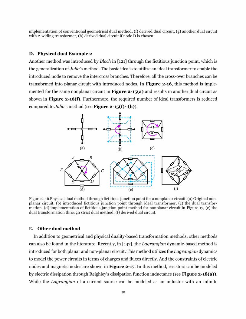
30
implementation of conventional geometrical dual method, (f) derived dual circuit, (g) another dual circuit with 2-widing transformer, (h) derived dual circuit if node D is chosen.
D. Physical dual Example 2
Another method was introduced by Bloch in [121] through the fictitious junction point, which is
the generalization of Julia’s method. The basic idea is to utilize an ideal transformer to enable the
introduced node to remove the intercross branches. Therefore, all the cross-over branches can be
transformed into planar circuit with introduced nodes. In Figure 2-16, this method is imple-
mented for the same nonplanar circuit in Figure 2-15(a) and results in another dual circuit as
shown in Figure 2-16(f). Furthermore, the required number of ideal transformers is reduced
compared to Julia’s method (see Figure 2-15(f)~(h)).
F
A B
C
DE
(a) (b) (c)
(d) (e) (f)
Figure 2-16 Physical dual method through fictitious junction point for a nonplanar circuit. (a) Original non-planar circuit, (b) introduced fictitious junction point through ideal transformer, (c) the dual transfor-mation, (d) implementation of fictitious junction point method for nonplanar circuit in Figure 17, (e) the dual transformation through strict dual method, (f) derived dual circuit.
E. Other dual method
In addition to geometrical and physical duality-based transformation methods, other methods
can also be found in the literature. Recently, in [147], the Lagrangian dynamic-based method is
introduced for both planar and non-planar circuit. This method utilizes the Lagrangian dynamics
to model the power circuits in terms of charges and fluxes directly. And the constraints of electric
nodes and magnetic nodes are shown in Figure 2-17. In this method, resistors can be modeled
by electric dissipation through Reighley’s dissipation function inductance (see Figure 2-18(a)).
While the Lagrangian of a current source can be modeled as an inductor with an infinite
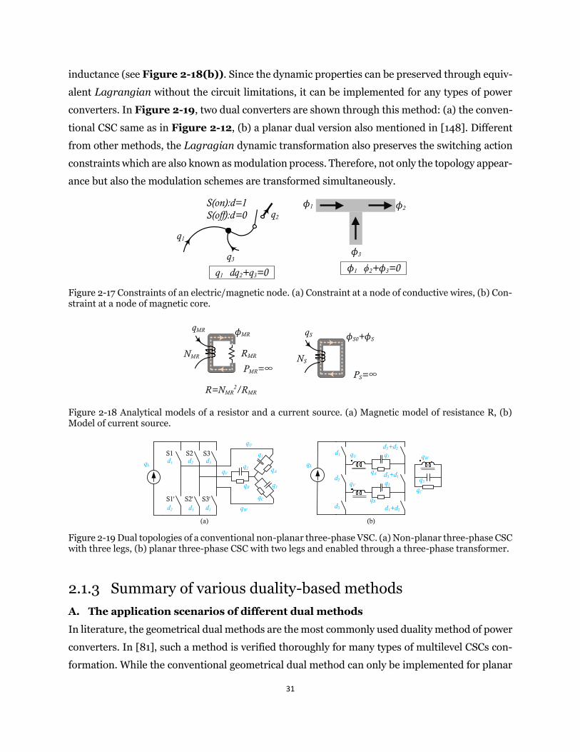
31
inductance (see Figure 2-18(b)). Since the dynamic properties can be preserved through equiv-
alent Lagrangian without the circuit limitations, it can be implemented for any types of power
converters. In Figure 2-19, two dual converters are shown through this method: (a) the conven-
tional CSC same as in Figure 2-12, (b) a planar dual version also mentioned in [148]. Different
from other methods, the Lagragian dynamic transformation also preserves the switching action
constraints which are also known as modulation process. Therefore, not only the topology appear-
ance but also the modulation schemes are transformed simultaneously.
q3
q1
S(on):d=1
S(off):d=0
q1 dq2+q3=0
ϕ1 ϕ2
ϕ3
ϕ1 ϕ2+ϕ3=0
q2
Figure 2-17 Constraints of an electric/magnetic node. (a) Constraint at a node of conductive wires, (b) Con-straint at a node of magnetic core.
qMR
ϕS0+ϕS
NMR RMR
R=NMR2/RMR
qS
NS
ϕMR
PMR= PS=
Figure 2-18 Analytical models of a resistor and a current source. (a) Magnetic model of resistance R, (b) Model of current source.
S1 S2 S3
S1' S2' S3'
d1
d1
d2
d3
d2 d3
q1
q2q3
qA
qB
qC
qU
qV
qW
d2 d1d3
qV
qU
qW
q1
q2
q3
qA
qB
qC
qλ qλ
d3+d1
d3+d2
d1+d2
(a) (b)
Figure 2-19 Dual topologies of a conventional non-planar three-phase VSC. (a) Non-planar three-phase CSC with three legs, (b) planar three-phase CSC with two legs and enabled through a three-phase transformer.
2.1.3 Summary of various duality-based methods
A. The application scenarios of different dual methods
In literature, the geometrical dual methods are the most commonly used duality method of power
converters. In [81], such a method is verified thoroughly for many types of multilevel CSCs con-
formation. While the conventional geometrical dual method can only be implemented for planar
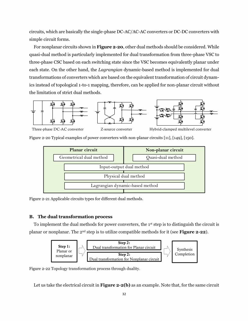
32
circuits, which are basically the single-phase DC-AC/AC-AC converters or DC-DC converters with
simple circuit forms.
For nonplanar circuits shown in Figure 2-20, other dual methods should be considered. While
quasi-dual method is particularly implemented for dual transformation from three-phase VSC to
three-phase CSC based on each switching state since the VSC becomes equivalently planar under
each state. On the other hand, the Lagrangian dynamic-based method is implemented for dual
transformations of converters which are based on the equivalent transformation of circuit dynam-
ics instead of topological 1-to-1 mapping, therefore, can be applied for non-planar circuit without
the limitation of strict dual methods.
Three-phase DC-AC converter Z-source converter Hybrid-clamped multilevel converter Figure 2-20 Typical examples of power converters with non-planar circuits [11], [149], [150].
Planar circuit Non-planar circuit
Geometrical dual method
Input-output dual method
Physical dual method
Lagrangian dynamic-based method
Quasi-dual method
Figure 2-21 Applicable circuits types for different dual methods.
B. The dual transformation process
To implement the dual methods for power converters, the 1st step is to distinguish the circuit is
planar or nonplanar. The 2nd step is to utilize compatible methods for it (see Figure 2-22).
Step 1: Planar or nonplanar
Step 2: Dual transformation for Planar circuit
Step 2: Dual transformation for Nonplanar circuit
SynthesisCompletion
Figure 2-22 Topology transformation process through duality.
Let us take the electrical circuit in Figure 2-2(b) as an example. Note that, for the same circuit
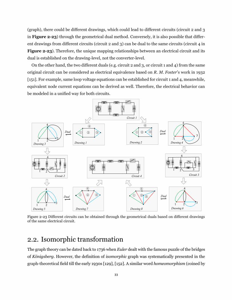
33
(graph), there could be different drawings, which could lead to different circuits (circuit 2 and 3
in Figure 2-23) through the geometrical dual method. Conversely, it is also possible that differ-
ent drawings from different circuits (circuit 2 and 3) can be dual to the same circuits (circuit 4 in
Figure 2-23). Therefore, the unique mapping relationships between an electrical circuit and its
dual is established on the drawing-level, not the converter-level.
On the other hand, the two different duals (e.g. circuit 2 and 3, or circuit 1 and 4) from the same
original circuit can be considered as electrical equivalence based on R. M. Foster’s work in 1932
[151]. For example, same loop voltage equations can be established for circuit 1 and 4, meanwhile,
equivalent node current equations can be derived as well. Therefore, the electrical behavior can
be modeled in a unified way for both circuits.
21
4
3 21
4
3
Drawing 1 Drawing 2
Dual
21
4
3 21
4
3
Dual
21
4
3 21
4
3
DualDual
Circuit 1
Circuit 2 Circuit 3Circuit 4
Drawing 3 Drawing 4
Drawing 5 Drawing 6Drawing 8Drawing 7 Figure 2-23 Different circuits can be obtained through the geometrical duals based on different drawings of the same electrical circuit.
2.2. Isomorphic transformation
The graph theory can be dated back to 1736 when Euler dealt with the famous puzzle of the bridges
of Königsberg. However, the definition of isomorphic graph was systematically presented in the
graph-theoretical field till the early 1930s [129], [152]. A similar word homeomorphism (coined by
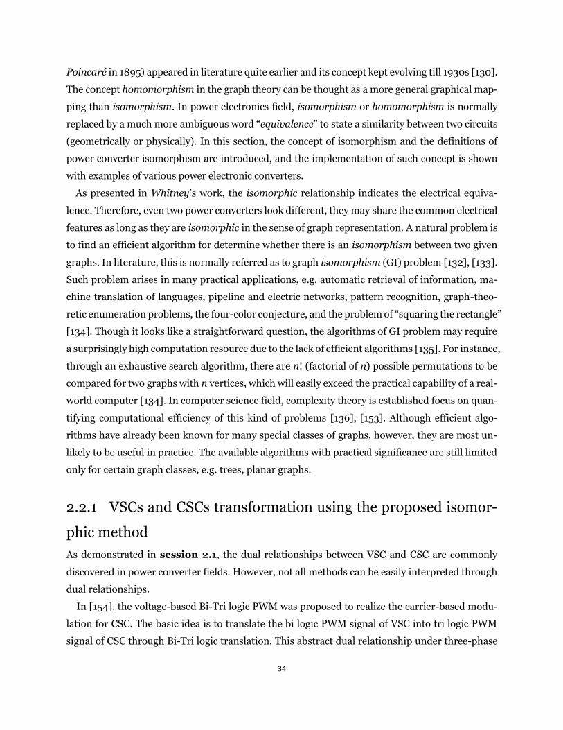
34
Poincaré in 1895) appeared in literature quite earlier and its concept kept evolving till 1930s [130].
The concept homomorphism in the graph theory can be thought as a more general graphical map-
ping than isomorphism. In power electronics field, isomorphism or homomorphism is normally
replaced by a much more ambiguous word “equivalence” to state a similarity between two circuits
(geometrically or physically). In this section, the concept of isomorphism and the definitions of
power converter isomorphism are introduced, and the implementation of such concept is shown
with examples of various power electronic converters.
As presented in Whitney’s work, the isomorphic relationship indicates the electrical equiva-
lence. Therefore, even two power converters look different, they may share the common electrical
features as long as they are isomorphic in the sense of graph representation. A natural problem is
to find an efficient algorithm for determine whether there is an isomorphism between two given
graphs. In literature, this is normally referred as to graph isomorphism (GI) problem [132], [133].
Such problem arises in many practical applications, e.g. automatic retrieval of information, ma-
chine translation of languages, pipeline and electric networks, pattern recognition, graph-theo-
retic enumeration problems, the four-color conjecture, and the problem of “squaring the rectangle”
[134]. Though it looks like a straightforward question, the algorithms of GI problem may require
a surprisingly high computation resource due to the lack of efficient algorithms [135]. For instance,
through an exhaustive search algorithm, there are n! (factorial of n) possible permutations to be
compared for two graphs with n vertices, which will easily exceed the practical capability of a real-
world computer [134]. In computer science field, complexity theory is established focus on quan-
tifying computational efficiency of this kind of problems [136], [153]. Although efficient algo-
rithms have already been known for many special classes of graphs, however, they are most un-
likely to be useful in practice. The available algorithms with practical significance are still limited
only for certain graph classes, e.g. trees, planar graphs.
2.2.1 VSCs and CSCs transformation using the proposed isomor-
phic method
As demonstrated in session 2.1, the dual relationships between VSC and CSC are commonly
discovered in power converter fields. However, not all methods can be easily interpreted through
dual relationships.
In [154], the voltage-based Bi-Tri logic PWM was proposed to realize the carrier-based modu-
lation for CSC. The basic idea is to translate the bi logic PWM signal of VSC into tri logic PWM
signal of CSC through Bi-Tri logic translation. This abstract dual relationship under three-phase
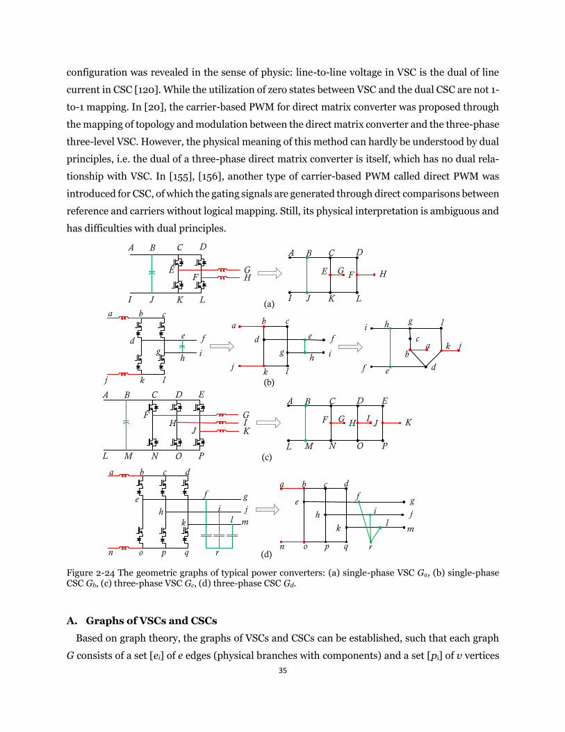
35
configuration was revealed in the sense of physic: line-to-line voltage in VSC is the dual of line
current in CSC [120]. While the utilization of zero states between VSC and the dual CSC are not 1-
to-1 mapping. In [20], the carrier-based PWM for direct matrix converter was proposed through
the mapping of topology and modulation between the direct matrix converter and the three-phase
three-level VSC. However, the physical meaning of this method can hardly be understood by dual
principles, i.e. the dual of a three-phase direct matrix converter is itself, which has no dual rela-
tionship with VSC. In [155], [156], another type of carrier-based PWM called direct PWM was
introduced for CSC, of which the gating signals are generated through direct comparisons between
reference and carriers without logical mapping. Still, its physical interpretation is ambiguous and
has difficulties with dual principles.
B C D
FE
K LJ
HG
A
I
b c
d fe
k lj
hg
a
i
B C D
E
K LJ
G
A
I(a)
(b)
b c
d fe
k lj
hg
a
i
B D E
H
O PM
IG
A
L
B C D
HF
N OM
IG
A
L
(c)
C
F
N
J K
E
P
KJ
b ca d
ef g
h i j
mlk
o pn q r
c d
h ji
p qn
lk
a
m
b
e
o
f g
r(d)
b
c
df e
k
l
j
h g
a
i
F H
Figure 2-24 The geometric graphs of typical power converters: (a) single-phase VSC Ga, (b) single-phase CSC Gb, (c) three-phase VSC Gc, (d) three-phase CSC Gd.
A. Graphs of VSCs and CSCs
Based on graph theory, the graphs of VSCs and CSCs can be established, such that each graph
G consists of a set [ei] of e edges (physical branches with components) and a set [pi] of v vertices
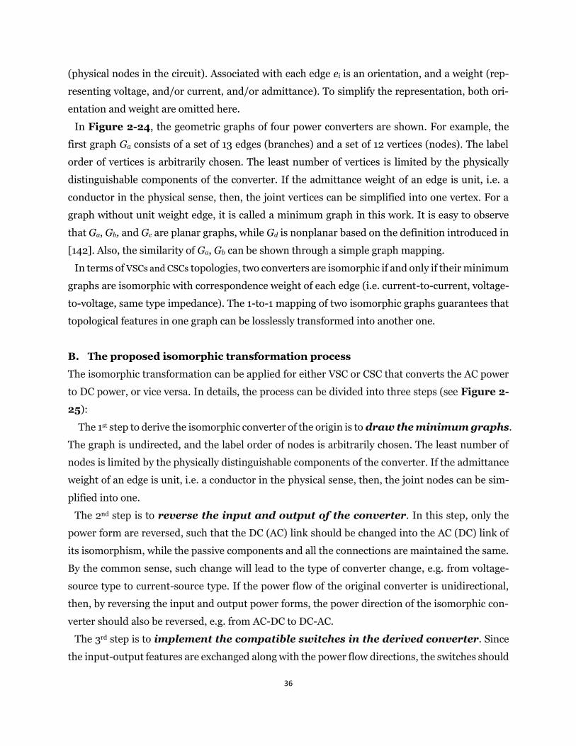
36
(physical nodes in the circuit). Associated with each edge ei is an orientation, and a weight (rep-
resenting voltage, and/or current, and/or admittance). To simplify the representation, both ori-
entation and weight are omitted here.
In Figure 2-24, the geometric graphs of four power converters are shown. For example, the
first graph Ga consists of a set of 13 edges (branches) and a set of 12 vertices (nodes). The label
order of vertices is arbitrarily chosen. The least number of vertices is limited by the physically
distinguishable components of the converter. If the admittance weight of an edge is unit, i.e. a
conductor in the physical sense, then, the joint vertices can be simplified into one vertex. For a
graph without unit weight edge, it is called a minimum graph in this work. It is easy to observe
that Ga, Gb, and Gc are planar graphs, while Gd is nonplanar based on the definition introduced in
[142]. Also, the similarity of Ga, Gb can be shown through a simple graph mapping.
In terms of VSCs and CSCs topologies, two converters are isomorphic if and only if their minimum
graphs are isomorphic with correspondence weight of each edge (i.e. current-to-current, voltage-
to-voltage, same type impedance). The 1-to-1 mapping of two isomorphic graphs guarantees that
topological features in one graph can be losslessly transformed into another one.
B. The proposed isomorphic transformation process
The isomorphic transformation can be applied for either VSC or CSC that converts the AC power
to DC power, or vice versa. In details, the process can be divided into three steps (see Figure 2-
25):
The 1st step to derive the isomorphic converter of the origin is to draw the minimum graphs.
The graph is undirected, and the label order of nodes is arbitrarily chosen. The least number of
nodes is limited by the physically distinguishable components of the converter. If the admittance
weight of an edge is unit, i.e. a conductor in the physical sense, then, the joint nodes can be sim-
plified into one.
The 2nd step is to reverse the input and output of the converter. In this step, only the
power form are reversed, such that the DC (AC) link should be changed into the AC (DC) link of
its isomorphism, while the passive components and all the connections are maintained the same.
By the common sense, such change will lead to the type of converter change, e.g. from voltage-
source type to current-source type. If the power flow of the original converter is unidirectional,
then, by reversing the input and output power forms, the power direction of the isomorphic con-
verter should also be reversed, e.g. from AC-DC to DC-AC.
The 3rd step is to implement the compatible switches in the derived converter. Since
the input-output features are exchanged along with the power flow directions, the switches should
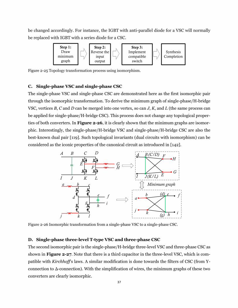
37
be changed accordingly. For instance, the IGBT with anti-parallel diode for a VSC will normally
be replaced with IGBT with a series diode for a CSC.
Step 1: Draw
minimum graph
Step 2: Reverse the
input output
Step 3: Implement compatible
switch
SynthesisCompletion
Figure 2-25 Topology transformation process using isomorphism.
C. Single-phase VSC and single-phase CSC
The single-phase VSC and single-phase CSC are demonstrated here as the first isomorphic pair
through the isomorphic transformation. To derive the minimum graph of single-phase/H-bridge
VSC, vertices B, C and D can be merged into one vertex, so can J, K, and L (the same process can
be applied for single-phase/H-bridge CSC). This process does not change any topological proper-
ties of both converters. In Figure 2-26, it is clearly shown that the minimum graphs are isomor-
phic. Interestingly, the single-phase/H-bridge VSC and single-phase/H-bridge CSC are also the
best-known dual pair [119]. Such topological invariants (dual circuits with isomorphism) can be
considered as the iconic properties of the canonical circuit as introduced in [142].
B (C/D) F
EJ
H
G
A
I (K/L)
B C D
FE
K LJ
HG
A
I
b c
d fe
k lj
hg
a
i
b (d) fe
kj
h(g)
a
i
Minimum graph
Figure 2-26 Isomorphic transformation from a single-phase VSC to a single-phase CSC.
D. Single-phase three-level T-type VSC and three-phase CSC
The second isomorphic pair is the single-phase/H-bridge three-level VSC and three-phase CSC as
shown in Figure 2-27. Note that there is a third capacitor in the three-level VSC, which is com-
patible with Kirchhoff’s laws. A similar modification is done towards the filters of CSC (from Y-
connection to Δ-connection). With the simplification of wires, the minimum graphs of these two
converters are clearly isomorphic.
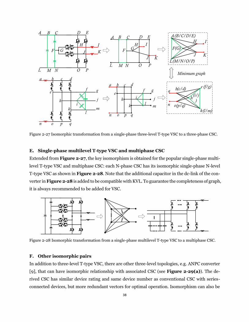
38
B D ECA
F G J K
M O PNL
b ca d
e g
h j
mk
o pn q
f
i
l
c d
h ji
p qn
lk
a
m
b
e
o
f g
BA C D E
F GH I
J
M NL O P
h(i/j
)n
k
a
(l/m)
(c/d) e
o
(f/g)
(B/C/D/E)A
F(G)
H
J K
L(M/N/O/P)
b
(p/q)
Minimum graph
H II
K
Figure 2-27 Isomorphic transformation from a single-phase three-level T-type VSC to a three-phase CSC.
E. Single-phase multilevel T-type VSC and multiphase CSC
Extended from Figure 2-27, the key isomorphism is obtained for the popular single-phase multi-
level T-type VSC and multiphase CSC: each N-phase CSC has its isomorphic single-phase N-level
T-type VSC as shown in Figure 2-28. Note that the additional capacitor in the dc-link of the con-
verter in Figure 2-28 is added to be compatible with KVL. To guarantee the completeness of graph,
it is always recommended to be added for VSC.
Figure 2-28 Isomorphic transformation from a single-phase multilevel T-type VSC to a multiphase CSC.
F. Other isomorphic pairs
In addition to three-level T-type VSC, there are other three-level topologies, e.g. ANPC converter
[9], that can have isomorphic relationship with associated CSC (see Figure 2-29(a)). The de-
rived CSC has similar device rating and same device number as conventional CSC with series-
connected devices, but more redundant vectors for optimal operation. Isomorphism can also be
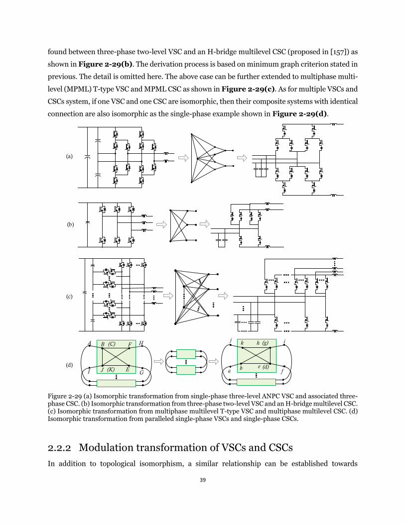
39
found between three-phase two-level VSC and an H-bridge multilevel CSC (proposed in [157]) as
shown in Figure 2-29(b). The derivation process is based on minimum graph criterion stated in
previous. The detail is omitted here. The above case can be further extended to multiphase multi-
level (MPML) T-type VSC and MPML CSC as shown in Figure 2-29(c). As for multiple VSCs and
CSCs system, if one VSC and one CSC are isomorphic, then their composite systems with identical
connection are also isomorphic as the single-phase example shown in Figure 2-29(d).
B (C) F
EJ
H
G
A
I (K) b (d)f
e
kj h (g)
a
i
(a)
(b)
(c)
(d)
Figure 2-29 (a) Isomorphic transformation from single-phase three-level ANPC VSC and associated three-phase CSC. (b) Isomorphic transformation from three-phase two-level VSC and an H-bridge multilevel CSC. (c) Isomorphic transformation from multiphase multilevel T-type VSC and multiphase multilevel CSC. (d) Isomorphic transformation from paralleled single-phase VSCs and single-phase CSCs.
2.2.2 Modulation transformation of VSCs and CSCs
In addition to topological isomorphism, a similar relationship can be established towards
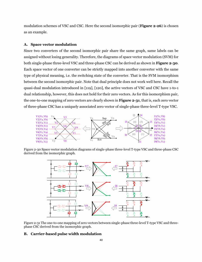
40
modulation schemes of VSC and CSC. Here the second isomorphic pair (Figure 2-26) is chosen
as an example.
A. Space vector modulation
Since two converters of the second isomorphic pair share the same graph, same labels can be
assigned without losing generality. Therefore, the diagrams of space vector modulation (SVM) for
both single-phase three-level VSC and three-phase CSC can be derived as shown in Figure 2-30.
Each space vector of one converter can be strictly mapped into another converter with the same
type of physical meaning, i.e. the switching state of the converter. That is the SVM isomorphism
between the second isomorphic pair. Note that dual principle does not work well here. Recall the
quasi-dual modulation introduced in [119], [120], the active vectors of VSC and CSC have 1-to-1
dual relationship, however, this does not hold for their zero vectors. As for this isomorphism pair,
the one-to-one mapping of zero vectors are clearly shown in Figure 2-31, that is, each zero vector
of three-phase CSC has a uniquely associated zero vector of single-phase three-level T-type VSC.
V2V8
V1
V7
V5
V6
V3
V4
V9
Vp
Vn
I2
I3
I7 (2)
(3)(4)
(5)
(6) (1)I6
I5
I1
I4
I7I8
I8 I9
I9 Iα
Iβ I1(Vc,Vb)I2(Va,Vb)I3(Va,Vc)I4(Vb,Vc)I5(Vb,Va)I6(Vc,Va)I7(Va,Va)I8(Vb,Vb)I9(Vc,Vc)
VpVa
Vb
VcVn
Sap
Scn
V1(Vc,Vb)V2(Va,Vb)V3(Va,Vc)V4(Vb,Vc)V5(Vb,Va)V6(Vc,Va)V7(Va,Va)V8(Vb,Vb)V9(Vc,Vc)
Figure 2-30 Space vector modulation diagrams of single-phase three-level T-type VSC and three-phase CSC derived from the isomorphic graph.
V7 I7
V8 I8
V9 I9
Figure 2-31 The one-to-one mapping of zero vectors between single-phase three-level T-type VSC and three-phase CSC derived from the isomorphic graph.
B. Carrier-based pulse width modulation
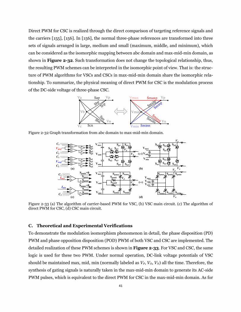
41
Direct PWM for CSC is realized through the direct comparison of targeting reference signals and
the carriers [155], [156]. In [156], the normal three-phase references are transformed into three
sets of signals arranged in large, medium and small (maximum, middle, and minimum), which
can be considered as the isomorphic mapping between abc domain and max-mid-min domain, as
shown in Figure 2-32. Such transformation does not change the topological relationship, thus,
the resulting PWM schemes can be interpreted in the isomorphic point of view. That is: the struc-
ture of PWM algorithms for VSCs and CSCs in max-mid-min domain share the isomorphic rela-
tionship. To summarize, the physical meaning of direct PWM for CSC is the modulation process
of the DC-side voltage of three-phase CSC.
VpVa
Vb
VcVn
Sap
Scn
VpVmax
Vmid
VminVn
Smaxp
Sminn
Figure 2-32 Graph transformation from abc domain to max-mid-min domain.
Sp2 Sp3
Sn2 Sn3
Sp1
Sp4
Sn1
Sn4
Vmax
Vmid
Vmin
Sp1
Sn1
Sp4
Sn4
Vmax
Vmid
Vmin Sn2
Sn3
Sp2
Sp3Vpref
+-C1 Sp1Sp3
Vnref Sn2Sn4
Vp
Vn
Vp
Vn(a)
Imax
Imin
+-
C1
C2
Spmin=0SpmaxSpmid
Snmax=0SnmidSnmin
SpmaxVmax
Vmid
Vmin
Vp
Vn
Spmid
Spmin
Snmax
Snmid
Snmin
Spmax Spmid Spmin
Snmax Snmid Snmin
Vp
Vn
VmaxVmidVmin
(b)
(c) (d)-+
C2-+ Sp2Sp4
+-C1
C2-+
Sn1Sn3
Figure 2-33 (a) The algorithm of carrier-based PWM for VSC, (b) VSC main circuit. (c) The algorithm of direct PWM for CSC, (d) CSC main circuit.
C. Theoretical and Experimental Verifications
To demonstrate the modulation isomorphism phenomenon in detail, the phase disposition (PD)
PWM and phase opposition disposition (POD) PWM of both VSC and CSC are implemented. The
detailed realization of these PWM schemes is shown in Figure 2-33. For VSC and CSC, the same
logic is used for these two PWM. Under normal operation, DC-link voltage potentials of VSC
should be maintained max, mid, min (normally labeled as VP, VO, VN) all the time. Therefore, the
synthesis of gating signals is naturally taken in the max-mid-min domain to generate its AC-side
PWM pulses, which is equivalent to the direct PWM for CSC in the max-mid-min domain. As for
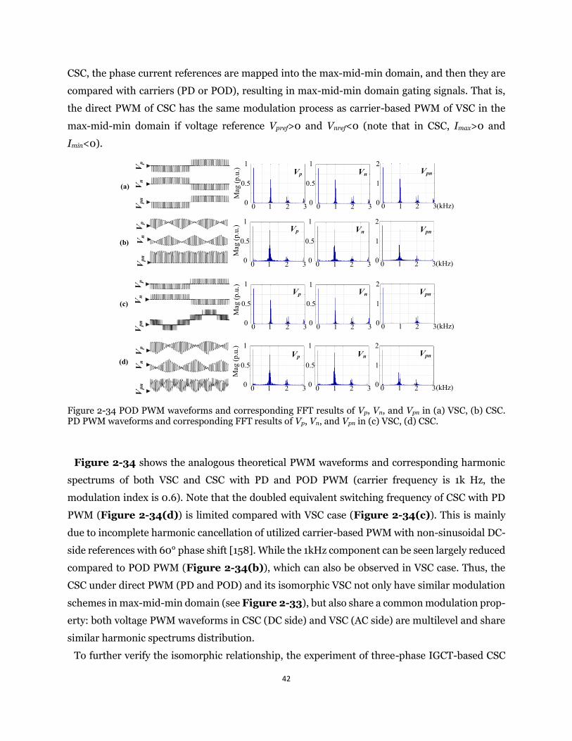
42
CSC, the phase current references are mapped into the max-mid-min domain, and then they are
compared with carriers (PD or POD), resulting in max-mid-min domain gating signals. That is,
the direct PWM of CSC has the same modulation process as carrier-based PWM of VSC in the
max-mid-min domain if voltage reference Vpref>0 and Vnref<0 (note that in CSC, Imax>0 and
Imin<0).
(b)
Vp
Vn
Vpn
Vp
Vn
Vpn
Vp
Vn
Vpn
(c)
(d)
(kHz)
0 1 2 3
Mag
(p.u
.)
0
1
0 1 2 30 1 2 3 0
1
2
0
1Vp Vn Vpn
0.5 0.5
0 1 2 3
Mag
(p.u
.)
0
1
0 1 2 30 1 2 3 0
1
2
0
1Vp Vn Vpn
0.5 0.5
0 1 2 3
Mag
(p.u
.)
0
1
0 1 2 30 1 2 3 0
1
2
0
1Vp Vn Vpn
0.5 0.5
(kHz)
(kHz)
(kHz)
Vp
Vn
Vpn
(a)
0 1 2 3
Mag
(p.u
.)
0
1
0 1 2 30 1 2 3 0
1
2
0
1Vp Vn Vpn
0.5 0.5
Figure 2-34 POD PWM waveforms and corresponding FFT results of Vp, Vn, and Vpn in (a) VSC, (b) CSC. PD PWM waveforms and corresponding FFT results of Vp, Vn, and Vpn in (c) VSC, (d) CSC.
Figure 2-34 shows the analogous theoretical PWM waveforms and corresponding harmonic
spectrums of both VSC and CSC with PD and POD PWM (carrier frequency is 1k Hz, the
modulation index is 0.6). Note that the doubled equivalent switching frequency of CSC with PD
PWM (Figure 2-34(d)) is limited compared with VSC case (Figure 2-34(c)). This is mainly
due to incomplete harmonic cancellation of utilized carrier-based PWM with non-sinusoidal DC-
side references with 60° phase shift [158]. While the 1kHz component can be seen largely reduced
compared to POD PWM (Figure 2-34(b)), which can also be observed in VSC case. Thus, the
CSC under direct PWM (PD and POD) and its isomorphic VSC not only have similar modulation
schemes in max-mid-min domain (see Figure 2-33), but also share a common modulation prop-
erty: both voltage PWM waveforms in CSC (DC side) and VSC (AC side) are multilevel and share
similar harmonic spectrums distribution.
To further verify the isomorphic relationship, the experiment of three-phase IGCT-based CSC
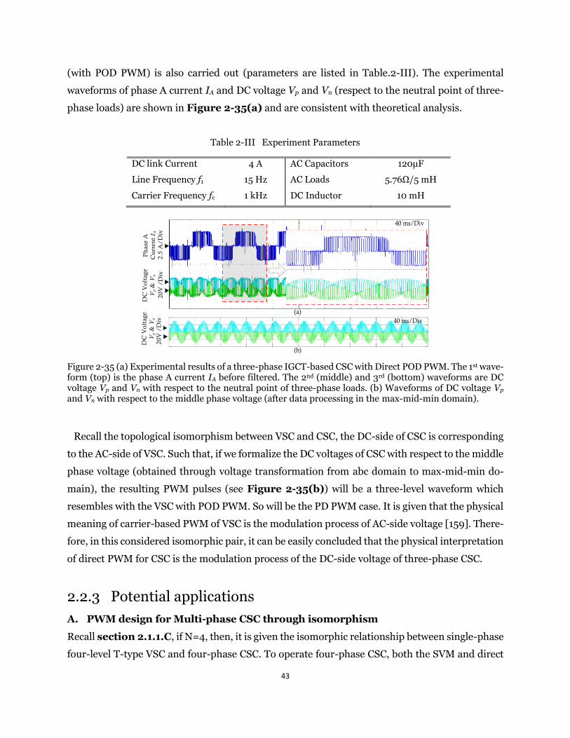
43
(with POD PWM) is also carried out (parameters are listed in Table.2-III). The experimental
waveforms of phase A current IA and DC voltage Vp and Vn (respect to the neutral point of three-
phase loads) are shown in Figure 2-35(a) and are consistent with theoretical analysis.
Table 2-III Experiment Parameters
DC link Current 4 A AC Capacitors 120μF
Line Frequency f1 15 Hz AC Loads 5.76Ω/5 mH
Carrier Frequency fc 1 kHz DC Inductor 10 mH
Ph
ase
A
Cu
rren
t I A
DC
Vo
ltag
e V
p &
Vn
2.5
A/D
iv20
V /
Div
40 ms/Div
20V
/D
iv
(a)
(b)
40 ms/Div
DC
Vo
ltag
e V
p &
Vn
Figure 2-35 (a) Experimental results of a three-phase IGCT-based CSC with Direct POD PWM. The 1st wave-form (top) is the phase A current IA before filtered. The 2nd (middle) and 3rd (bottom) waveforms are DC voltage Vp and Vn with respect to the neutral point of three-phase loads. (b) Waveforms of DC voltage Vp and Vn with respect to the middle phase voltage (after data processing in the max-mid-min domain).
Recall the topological isomorphism between VSC and CSC, the DC-side of CSC is corresponding
to the AC-side of VSC. Such that, if we formalize the DC voltages of CSC with respect to the middle
phase voltage (obtained through voltage transformation from abc domain to max-mid-min do-
main), the resulting PWM pulses (see Figure 2-35(b)) will be a three-level waveform which
resembles with the VSC with POD PWM. So will be the PD PWM case. It is given that the physical
meaning of carrier-based PWM of VSC is the modulation process of AC-side voltage [159]. There-
fore, in this considered isomorphic pair, it can be easily concluded that the physical interpretation
of direct PWM for CSC is the modulation process of the DC-side voltage of three-phase CSC.
2.2.3 Potential applications
A. PWM design for Multi-phase CSC through isomorphism
Recall section 2.1.1.C, if N=4, then, it is given the isomorphic relationship between single-phase
four-level T-type VSC and four-phase CSC. To operate four-phase CSC, both the SVM and direct
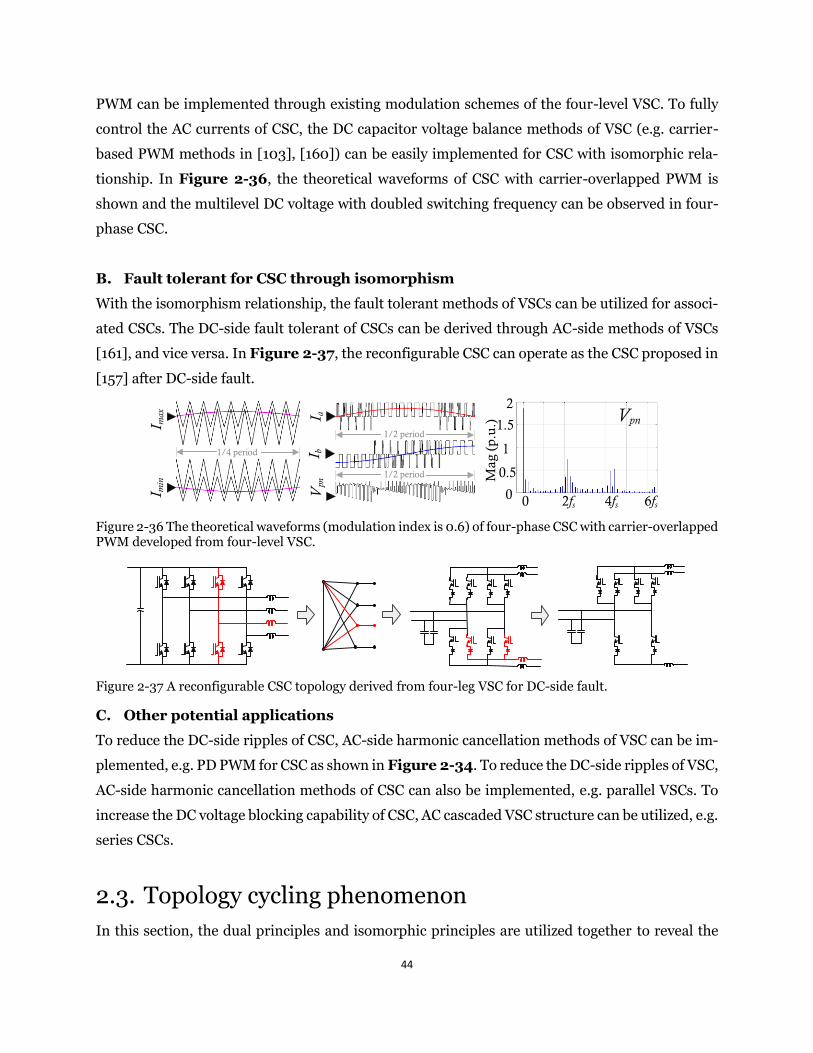
44
PWM can be implemented through existing modulation schemes of the four-level VSC. To fully
control the AC currents of CSC, the DC capacitor voltage balance methods of VSC (e.g. carrier-
based PWM methods in [103], [160]) can be easily implemented for CSC with isomorphic rela-
tionship. In Figure 2-36, the theoretical waveforms of CSC with carrier-overlapped PWM is
shown and the multilevel DC voltage with doubled switching frequency can be observed in four-
phase CSC.
B. Fault tolerant for CSC through isomorphism
With the isomorphism relationship, the fault tolerant methods of VSCs can be utilized for associ-
ated CSCs. The DC-side fault tolerant of CSCs can be derived through AC-side methods of VSCs
[161], and vice versa. In Figure 2-37, the reconfigurable CSC can operate as the CSC proposed in
[157] after DC-side fault.
I aI b
Vpn M
ag (
p.u.
)0
1
1.5
0 2fs
Vpn
0.5
2
4fs 6fs
I max
I min
1/4 period
1/2 period
1/2 period
Figure 2-36 The theoretical waveforms (modulation index is 0.6) of four-phase CSC with carrier-overlapped PWM developed from four-level VSC.
Figure 2-37 A reconfigurable CSC topology derived from four-leg VSC for DC-side fault.
C. Other potential applications
To reduce the DC-side ripples of CSC, AC-side harmonic cancellation methods of VSC can be im-
plemented, e.g. PD PWM for CSC as shown in Figure 2-34. To reduce the DC-side ripples of VSC,
AC-side harmonic cancellation methods of CSC can also be implemented, e.g. parallel VSCs. To
increase the DC voltage blocking capability of CSC, AC cascaded VSC structure can be utilized, e.g.
series CSCs.
2.3. Topology cycling phenomenon
In this section, the dual principles and isomorphic principles are utilized together to reveal the
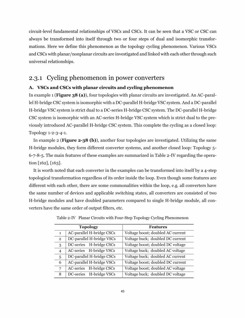
45
circuit-level fundamental relationships of VSCs and CSCs. It can be seen that a VSC or CSC can
always be transformed into itself through two or four steps of dual and isomorphic transfor-
mations. Here we define this phenomenon as the topology cycling phenomenon. Various VSCs
and CSCs with planar/nonplanar circuits are investigated and linked with each other through such
universal relationships.
2.3.1 Cycling phenomenon in power converters
A. VSCs and CSCs with planar circuits and cycling phenomenon
In example 1 (Figure 38 (a)), four topologies with planar circuits are investigated. An AC-paral-
lel H-bridge CSC system is isomorphic with a DC-parallel H-bridge VSC system. And a DC-parallel
H-bridge VSC system is strict dual to a DC-series H-bridge CSC system. The DC-parallel H-bridge
CSC system is isomorphic with an AC-series H-bridge VSC system which is strict dual to the pre-
viously introduced AC-parallel H-bridge CSC system. This complete the cycling as a closed loop:
Topology 1-2-3-4-1.
In example 2 (Figure 2-38 (b)), another four topologies are investigated. Utilizing the same
H-bridge modules, they form different converter systems, and another closed loop: Topology 5-
6-7-8-5. The main features of these examples are summarized in Table 2-IV regarding the opera-
tion [162], [163].
It is worth noted that each converter in the examples can be transformed into itself by a 4-step
topological transformation regardless of its order inside the loop. Even though some features are
different with each other, there are some commonalities within the loop, e.g. all converters have
the same number of devices and applicable switching states, all converters are consisted of two
H-bridge modules and have doubled parameters compared to single H-bridge module, all con-
verters have the same order of output filters, etc.
Table 2-IV Planar Circuits with Four-Step Topology Cycling Phenomenon
Topology Features
1 AC-parallel H-bridge CSCs Voltage boost; doubled AC current
2 DC-parallel H-bridge VSCs Voltage buck; doubled DC current
3 DC-series H-bridge CSCs Voltage boost; doubled DC voltage
4 AC-series H-bridge VSCs Voltage buck; doubled AC voltage
5 DC-parallel H-bridge CSCs Voltage buck; doubled AC current
6 AC-parallel H-bridge VSCs Voltage boost; doubled DC current
7 AC-series H-bridge CSCs Voltage boost; doubled AC voltage
8 DC-series H-bridge VSCs Voltage buck; doubled DC voltage
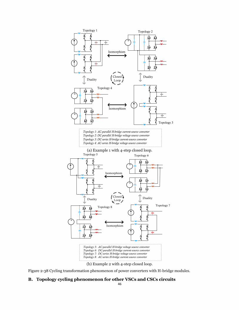
46
+
Topology 1 Topology 2
Topology 4
Topology 3
Isomorphism
Topology 1: AC-parallel H-bridge current-source converterTopology 2: DC-parallel H-bridge voltage-source converter
ClosedLoop
Duality
Isomorphism
Duality
Topology 3: DC-series H-bridge current-source converterTopology 4: AC-series H-bridge voltage-source converter
+
+
(a) Example 1 with 4-step closed loop.
Topology 5 Topology 6
Topology 8 Topology 7
Isomorphism
Topology 7: DC-series H-bridge voltage-source converterTopology 8: AC-series H-bridge current-source converter
ClosedLoop
Duality
Isomorphism
Duality
+
Topology 5: AC-parallel H-bridge voltage-source converterTopology 6: DC-parallel H-bridge current-source converter
+
+
(b) Example 2 with 4-step closed loop.
Figure 2-38 Cycling transformation phenomenon of power converters with H-bridge modules.
B. Topology cycling phenomenon for other VSCs and CSCs circuits
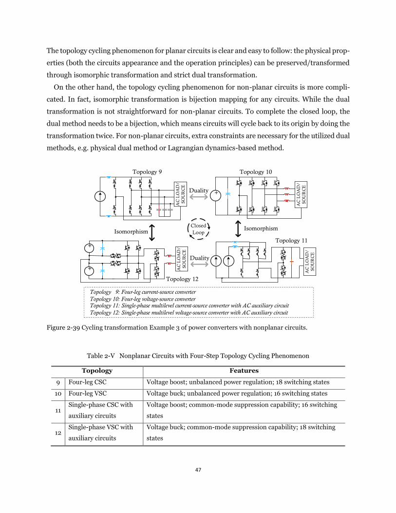
47
The topology cycling phenomenon for planar circuits is clear and easy to follow: the physical prop-
erties (both the circuits appearance and the operation principles) can be preserved/transformed
through isomorphic transformation and strict dual transformation.
On the other hand, the topology cycling phenomenon for non-planar circuits is more compli-
cated. In fact, isomorphic transformation is bijection mapping for any circuits. While the dual
transformation is not straightforward for non-planar circuits. To complete the closed loop, the
dual method needs to be a bijection, which means circuits will cycle back to its origin by doing the
transformation twice. For non-planar circuits, extra constraints are necessary for the utilized dual
methods, e.g. physical dual method or Lagrangian dynamics-based method.
Topology 9 Topology 10
Topology 12
Topology 11
Isomorphism
Topology 9: Four-leg current-source converterTopology 10: Four-leg voltage-source converter
ClosedLoop
Duality
Topology 11: Single-phase multilevel current-source converter with AC auxiliary circuitTopology 12: Single-phase multilevel voltage-source converter with AC auxiliary circuit
AC
LO
AD
/SO
UR
CE
+
AC
LO
AD
/SO
UR
CE
+
+
AC
LO
AD
/SO
UR
CE
AC
LO
AD
/SO
UR
CE
Duality
Isomorphism
Figure 2-39 Cycling transformation Example 3 of power converters with nonplanar circuits.
Table 2-V Nonplanar Circuits with Four-Step Topology Cycling Phenomenon
Topology Features
9 Four-leg CSC Voltage boost; unbalanced power regulation; 18 switching states
10 Four-leg VSC Voltage buck; unbalanced power regulation; 16 switching states
11 Single-phase CSC with
auxiliary circuits
Voltage boost; common-mode suppression capability; 16 switching
states
12 Single-phase VSC with
auxiliary circuits
Voltage buck; common-mode suppression capability; 18 switching
states
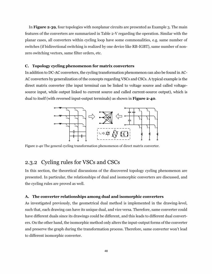
48
In Figure 2-39, four topologies with nonplanar circuits are presented as Example 3. The main
features of the converters are summarized in Table 2-V regarding the operation. Similar with the
planar cases, all converters within cycling loop have some commonalities, e.g. same number of
switches (if bidirectional switching is realized by one device like RB-IGBT), same number of non-
zero switching vectors, same filter orders, etc.
C. Topology cycling phenomenon for matrix converters
In addition to DC-AC converters, the cycling transformation phenomenon can also be found in AC-
AC converters by generalization of the concepts regarding VSCs and CSCs. A typical example is the
direct matrix converter (the input terminal can be linked to voltage source and called voltage-
source input, while output linked to current source and called current-source output), which is
dual to itself (with reversed input-output terminals) as shown in Figure 2-40.
Figure 2-40 The general cycling transformation phenomenon of direct matrix converter.
2.3.2 Cycling rules for VSCs and CSCs
In this section, the theoretical discussions of the discovered topology cycling phenomenon are
presented. In particular, the relationships of dual and isomorphic converters are discussed, and
the cycling rules are proved as well.
A. The converter relationships among dual and isomorphic converters
As investigated previously, the geometrical dual method is implemented in the drawing-level,
such that, each drawing can have its unique dual, and vice versa. Therefore, same converter could
have different duals since its drawings could be different, and this leads to different dual convert-
ers. On the other hand, the isomorphic method only alters the input-output forms of the converter
and preserve the graph during the transformation process. Therefore, same converter won’t lead
to different isomorphic converter.
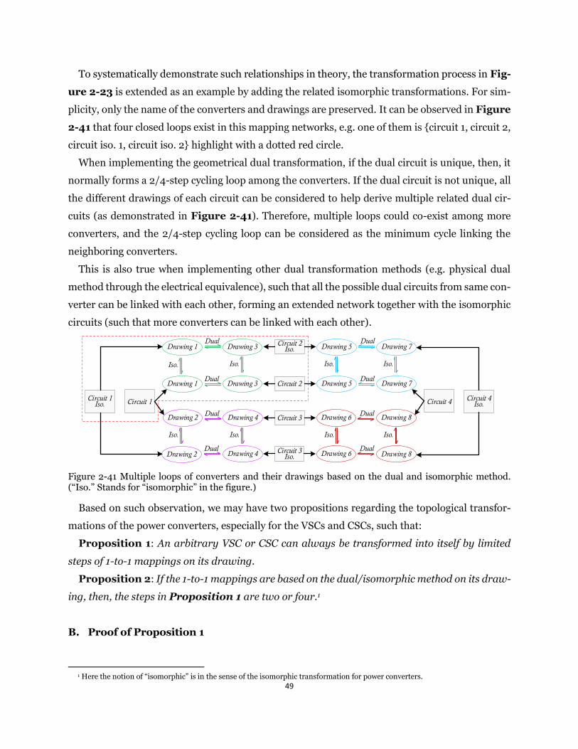
49
To systematically demonstrate such relationships in theory, the transformation process in Fig-
ure 2-23 is extended as an example by adding the related isomorphic transformations. For sim-
plicity, only the name of the converters and drawings are preserved. It can be observed in Figure
2-41 that four closed loops exist in this mapping networks, e.g. one of them is {circuit 1, circuit 2,
circuit iso. 1, circuit iso. 2} highlight with a dotted red circle.
When implementing the geometrical dual transformation, if the dual circuit is unique, then, it
normally forms a 2/4-step cycling loop among the converters. If the dual circuit is not unique, all
the different drawings of each circuit can be considered to help derive multiple related dual cir-
cuits (as demonstrated in Figure 2-41). Therefore, multiple loops could co-exist among more
converters, and the 2/4-step cycling loop can be considered as the minimum cycle linking the
neighboring converters.
This is also true when implementing other dual transformation methods (e.g. physical dual
method through the electrical equivalence), such that all the possible dual circuits from same con-
verter can be linked with each other, forming an extended network together with the isomorphic
circuits (such that more converters can be linked with each other).
Circuit 1
Drawing 1
Drawing 2
DualDrawing 3
Drawing 4Dual
Circuit 2
Circuit 3
Circuit 4
Drawing 7
Drawing 8
DualDrawing 5
Drawing 6Dual
Iso.
Drawing 2 Drawing 4 Drawing 6
Iso. Iso. Iso.
Drawing 8
Drawing 1 Drawing 3 Drawing 7Drawing 5
Iso. Iso. Iso. Iso.
Circuit 3Iso.
Circuit 2Iso.
Circuit 1Iso.
Circuit 4Iso.
Dual Dual
Dual Dual
Figure 2-41 Multiple loops of converters and their drawings based on the dual and isomorphic method. (“Iso.” Stands for “isomorphic” in the figure.)
Based on such observation, we may have two propositions regarding the topological transfor-
mations of the power converters, especially for the VSCs and CSCs, such that:
Proposition 1: An arbitrary VSC or CSC can always be transformed into itself by limited
steps of 1-to-1 mappings on its drawing.
Proposition 2: If the 1-to-1 mappings are based on the dual/isomorphic method on its draw-
ing, then, the steps in Proposition 1 are two or four.1
B. Proof of Proposition 1
1 Here the notion of “isomorphic” is in the sense of the isomorphic transformation for power converters.

50
First, define the 1-to-1 mapping of the drawings of VSCs and CSCs as the morphism between
objects A and B, such that, all the properties of A (a1, a2,…) are mapped into the associated prop-
erties of B (b1, b2,…) through T, and (b1, b2,…) can be mapped into (a1, a2,…) through the reverse
process of T, named T-1. This is also presented as follows:
(2-6)
Such mapping relationships will satisfy composition law:
(2-7)
The symbol “◦” means a composed action of two transformations. Obviously, isomorphic trans-
formation is a 1-to-1 mapping for any circuits based on this definition (e.g. Figure 2-42). Note
that the isomorphic transformation in this work is particularly designed for the power converter,
such that, the minimum graph of the converters are maintain the same after the transformation.
Dual transformation is 1-to-1 mapping for planar circuits on the drawing-level1, and conditional
1-to-1 mapping for nonplanar circuits (additional constraints like the dual voltage/current rela-
tionships using ideal transformer or the three-phase balanced output, as introduced in section
2.1.2).
Figure 2-42 1-to-1 mapping of isomorphic transformation.
(i) Proof of sufficient conditions:
Given limited steps of 1-to-1 mappings,
(2-8)
Define the mapping T=T1◦T2···, then, A can be transformed into itself by T◦T-1, which proves
an arbitrary drawing of converter can always be transformed into itself by given limited steps of
1-to-1 mappings.
1 This is true since each circuit is drawn in the way that there is unique 1-to-1 mappings between the circuit and its drawing in any
dual pair.
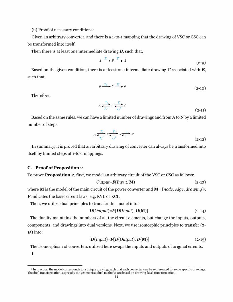
51
(ii) Proof of necessary conditions:
Given an arbitrary converter, and there is a 1-to-1 mapping that the drawing of VSC or CSC can
be transformed into itself.
Then there is at least one intermediate drawing B, such that,
(2-9)
Based on the given condition, there is at least one intermediate drawing C associated with B,
such that,
(2-10)
Therefore,
(2-11)
Based on the same rules, we can have a limited number of drawings and from A to N by a limited
number of steps:
(2-12)
In summary, it is proved that an arbitrary drawing of converter can always be transformed into
itself by limited steps of 1-to-1 mappings.
C. Proof of Proposition 2
To prove Proposition 2, first, we model an arbitrary circuit of the VSC or CSC as follows:
Output=F(Input, M) (2-13)
where M is the model of the main circuit of the power converter and M= [node, edge, drawing]1,
F indicates the basic circuit laws, e.g. KVL or KCL.
Then, we utilize dual principles to transfer this model into:
D(Output)=F[D(Input), D(M)] (2-14)
The duality maintains the numbers of all the circuit elements, but change the inputs, outputs,
components, and drawings into dual versions. Next, we use isomorphic principles to transfer (2-
15) into:
D(Input)=F[D(Output), D(M)] (2-15)
The isomorphism of converters utilized here swaps the inputs and outputs of original circuits.
If
1 In practice, the model corresponds to a unique drawing, such that each converter can be represented by some specific drawings.
The dual transformation, especially the geometrical dual methods, are based on drawing-level transformation.
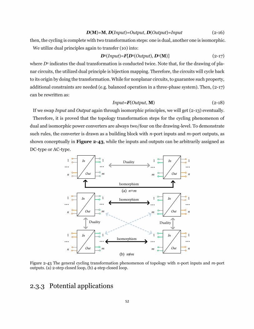
52
D(M)=M, D(Input)=Output, D(Output)=Input (2-16)
then, the cycling is complete with two transformation steps: one is dual, another one is isomorphic.
We utilize dual principles again to transfer (10) into:
D2(Input)=F[D2(Output), D2(M)] (2-17)
where D2 indicates the dual transformation is conducted twice. Note that, for the drawing of pla-
nar circuits, the utilized dual principle is bijection mapping. Therefore, the circuits will cycle back
to its origin by doing the transformation. While for nonplanar circuits, to guarantee such property,
additional constraints are needed (e.g. balanced operation in a three-phase system). Then, (2-17)
can be rewritten as:
Input=F(Output, M) (2-18)
If we swap Input and Output again through isomorphic principles, we will get (2-13) eventually.
Therefore, it is proved that the topology transformation steps for the cycling phenomenon of
dual and isomorphic power converters are always two/four on the drawing-level. To demonstrate
such rules, the converter is drawn as a building block with n-port inputs and m-port outputs, as
shown conceptually in Figure 2-43, while the inputs and outputs can be arbitrarily assigned as
DC-type or AC-type.
1
n
1
m
1
m
1
n
1
m
1
n
1
n
1
m
Isomorphism
Duality
Isomorphism
1
n
1
m
1
m
1
n
In
Out
Duality
Isomorphism
In
Out
In
Out
In
Out
In
Out
In
Out
Duality
(a) n=m
(b) n m
Figure 2-43 The general cycling transformation phenomenon of topology with n-port inputs and m-port outputs. (a) 2-step closed loop, (b) 4-step closed loop.
2.3.3 Potential applications
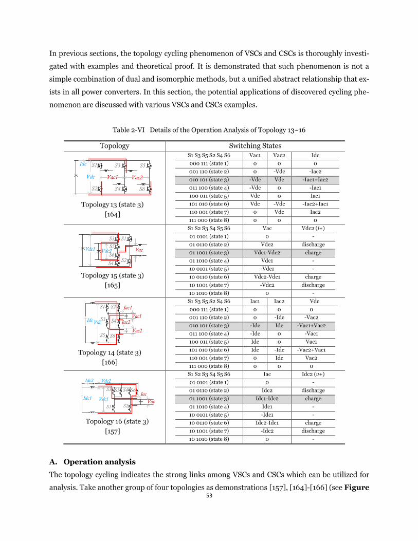
53
In previous sections, the topology cycling phenomenon of VSCs and CSCs is thoroughly investi-
gated with examples and theoretical proof. It is demonstrated that such phenomenon is not a
simple combination of dual and isomorphic methods, but a unified abstract relationship that ex-
ists in all power converters. In this section, the potential applications of discovered cycling phe-
nomenon are discussed with various VSCs and CSCs examples.
Table 2-VI Details of the Operation Analysis of Topology 13~16
Topology Switching States
S1
S2
S3
S4
S5
S6
Vac1 Vac2Vdc
Idc
Topology 13 (state 3)
[164]
S1 S3 S5 S2 S4 S6 Vac1 Vac2 Idc
000 111 (state 1) 0 0 0
001 110 (state 2) 0 -Vdc -Iac2
010 101 (state 3) -Vdc Vdc -Iac1+Iac2
011 100 (state 4) -Vdc 0 -Iac1
100 011 (state 5) Vdc 0 Iac1
101 010 (state 6) Vdc -Vdc -Iac2+Iac1
110 001 (state 7) 0 Vdc Iac2
111 000 (state 8) 0 0 0
S1
S2
S3
S4
S5
S6
Topology 15 (state 3)
[165]
S1 S2 S3 S4 S5 S6 Vac Vdc2 (i+)
01 0101 (state 1) 0 -
01 0110 (state 2) Vdc2 discharge
01 1001 (state 3) Vdc1-Vdc2 charge
01 1010 (state 4) Vdc1 -
10 0101 (state 5) -Vdc1 -
10 0110 (state 6) Vdc2-Vdc1 charge
10 1001 (state 7) -Vdc2 discharge
10 1010 (state 8) 0 -
Idc
Iac1
Iac2
S1 S2
S3 S4
S5 S6
Vdc
Topology 14 (state 3)
[166]
S1 S3 S5 S2 S4 S6 Iac1 Iac2 Vdc
000 111 (state 1) 0 0 0
001 110 (state 2) 0 -Idc -Vac2
010 101 (state 3) -Idc Idc -Vac1+Vac2
011 100 (state 4) -Idc 0 -Vac1
100 011 (state 5) Idc 0 Vac1
101 010 (state 6) Idc -Idc -Vac2+Vac1
110 001 (state 7) 0 Idc Vac2
111 000 (state 8) 0 0 0
IacIdc1
S5S3
S1
S6S4
S2
Idc2
Topology 16 (state 3)
[157]
S1 S2 S3 S4 S5 S6 Iac Idc2 (v+)
01 0101 (state 1) 0 -
01 0110 (state 2) Idc2 discharge
01 1001 (state 3) Idc1-Idc2 charge
01 1010 (state 4) Idc1 -
10 0101 (state 5) -Idc1 -
10 0110 (state 6) Idc2-Idc1 charge
10 1001 (state 7) -Idc2 discharge
10 1010 (state 8) 0 -
A. Operation analysis
The topology cycling indicates the strong links among VSCs and CSCs which can be utilized for
analysis. Take another group of four topologies as demonstrations [157], [164]-[166] (see Figure
54
2-44). Since they are planar circuits, strict mapping relationships are expected for all of them, e.g.
same numbers of switching vectors (eight vectors), same (dual) operation limitations of isomor-
phic (dual) circuits, etc. Based on such interconnections, operation analysis can be done with not
only the neighboring topologies but also any pair of topologies inside this loop, e.g. AC currents
of Topology 13 and DC voltages of Topology 15, AC voltages of Topology 14 and DC currents of
Topology 16.
The detailed features of them are summarized in Table. 2-VI. All four topologies share asso-
ciated AC/DC physical meanings using the same switching tables, e.g., state 3 of topology 15 can
be used to charge the Vdc2, while the same state of topology 16 leads to charge of Idc2, which implies
a similar voltage/current balancing scheme can be implemented for both topologies.
The detailed waveforms of DC current of Topology 13, DC voltage of Topology 14, AC voltage of
Topology 15 and DC current of Topology 16 are demonstrated in Figure 2-45 using the same
switching signals (see Figure 2-46). The operation principles are based on the conventional
modulation of Topology 15, a hybrid phase-shifted scheme, as introduced in [167]. The resulting
waveforms show strong similarities in all four topologies. Using proper selected DC-source values,
the shapes of Idc of Topology 13 and the Vdc of Topology 14 are the same; the shapes of Vac of
Topology 15 and the Iac of Topology 16 are the same as well. Through the FFT analysis (see Figure
2-47), all these waveforms have a similar harmonic spectrum in theory: the same equivalent
switching frequency which is doubled of the carrier frequency. Such performances further show
the general similarities of operations among the studied topologies.
+
AC LOAD/SOURCE
AC LOAD/SOURCE
AC LOAD/SOURCE
AC LOAD/SOURCE
Topology 13 Topology 14
+
+
AC LOAD/SOURCE
Topology 15
AC LOAD/SOURCE
Topology 16
Isomorphism
Duality
IsomorphismClosedLoop
Topology 13: Three-leg voltage-source converter with dual AC outputsTopology 14: Six-switch current-source converter with dual AC outputsTopology 15: Single-phase multilevel voltage-source converter with dual DC inputsTopology 16: Single-phase multilevel current-source converter with dual DC inputs
Duality
Figure 2-44 The topological transformation cycling Example 3.
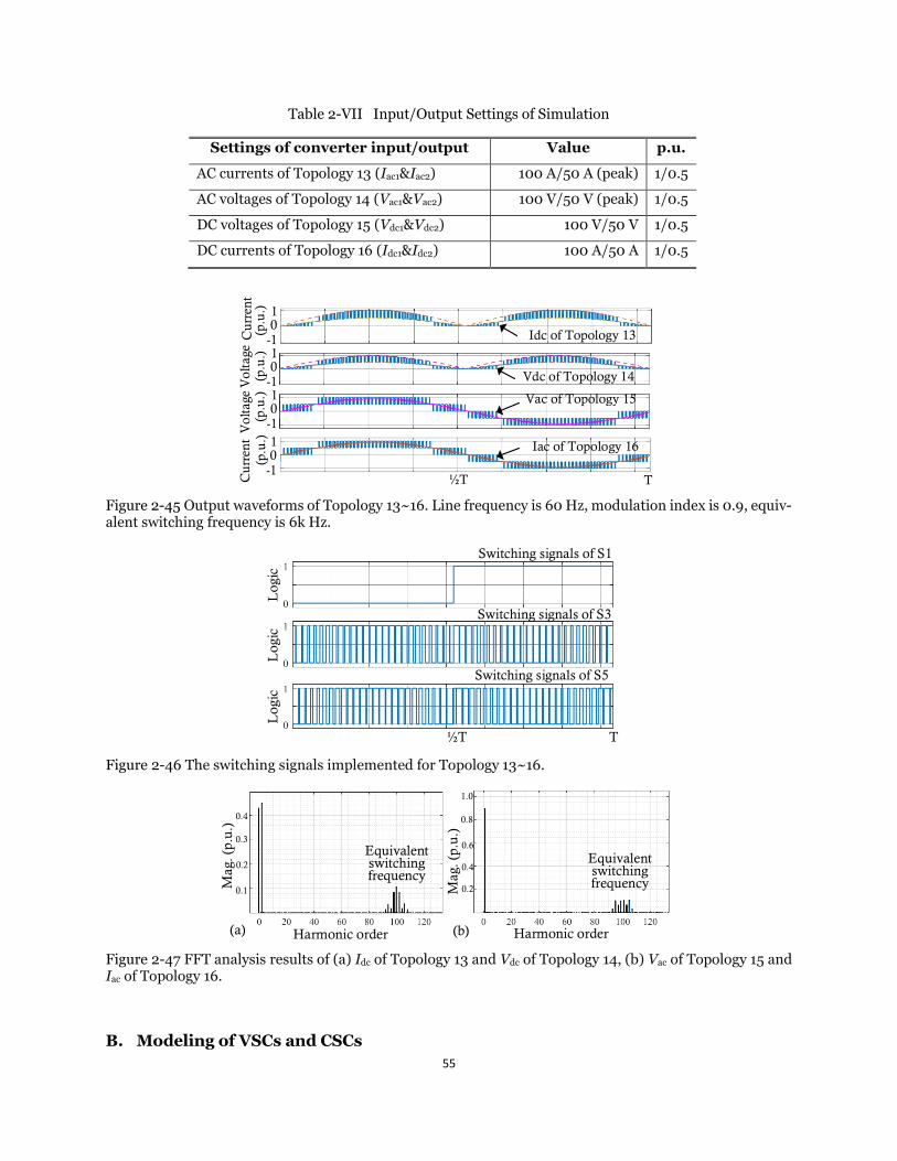
55
Table 2-VII Input/Output Settings of Simulation
Settings of converter input/output Value p.u.
AC currents of Topology 13 (Iac1&Iac2) 100 A/50 A (peak) 1/0.5
AC voltages of Topology 14 (Vac1&Vac2) 100 V/50 V (peak) 1/0.5
DC voltages of Topology 15 (Vdc1&Vdc2) 100 V/50 V 1/0.5
DC currents of Topology 16 (Idc1&Idc2) 100 A/50 A 1/0.5
Vac of Topology 15
Vdc of Topology 14
Iac of Topology 16
Idc of Topology 13(p.u
.) 10
-1
½T T
10
-110
-110
-1
(p.u
.)(p
.u.)
(p.u
.)C
urre
ntC
urre
ntV
olta
geV
olta
ge
Figure 2-45 Output waveforms of Topology 13~16. Line frequency is 60 Hz, modulation index is 0.9, equiv-alent switching frequency is 6k Hz.
Switching signals of S3
Switching signals of S5
Switching signals of S1
½T T
Log
icL
ogic
Log
ic
Figure 2-46 The switching signals implemented for Topology 13~16.
Equivalent switching frequency
Harmonic order Harmonic order
Equivalent switching frequency
(b)(a)
Mag
. (p.
u.)
0.4
0.1
0.2
0.3
Mag
. (p.
u.)
0.4
0.2
0.6
0.8
1.0
Figure 2-47 FFT analysis results of (a) Idc of Topology 13 and Vdc of Topology 14, (b) Vac of Topology 15 and Iac of Topology 16.
B. Modeling of VSCs and CSCs
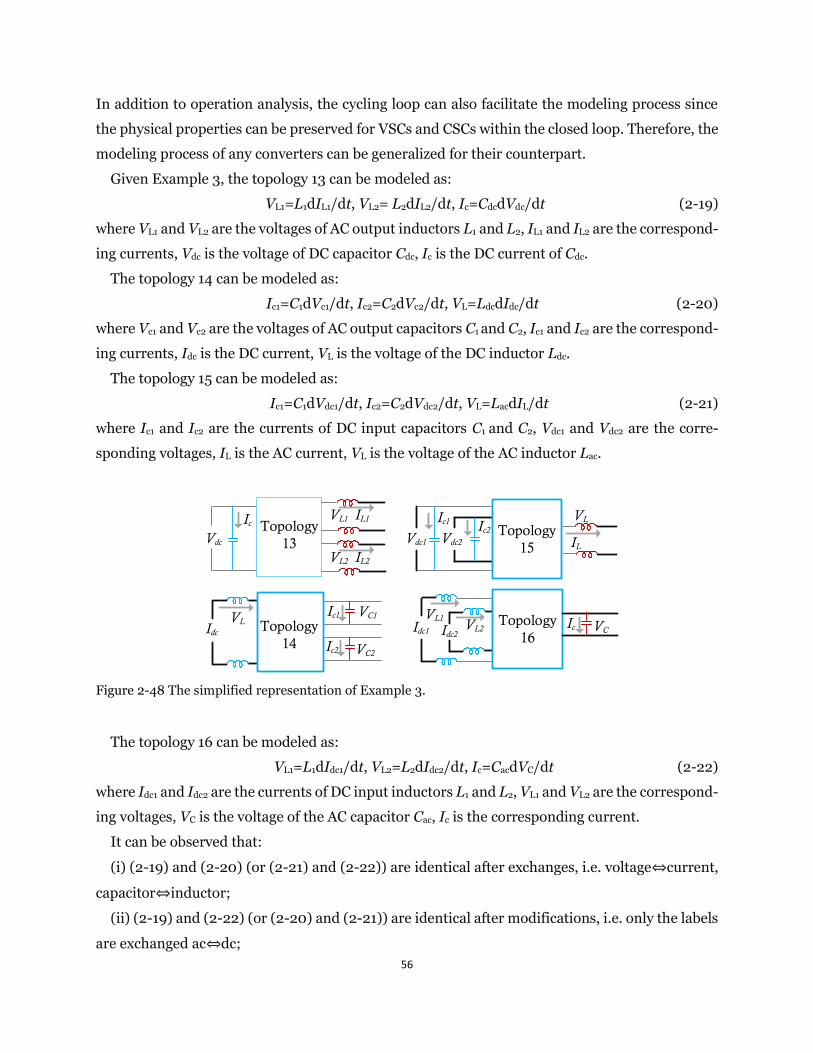
56
In addition to operation analysis, the cycling loop can also facilitate the modeling process since
the physical properties can be preserved for VSCs and CSCs within the closed loop. Therefore, the
modeling process of any converters can be generalized for their counterpart.
Given Example 3, the topology 13 can be modeled as:
VL1=L1dIL1/dt, VL2= L2dIL2/dt, Ic=CdcdVdc/dt (2-19)
where VL1 and VL2 are the voltages of AC output inductors L1 and L2, IL1 and IL2 are the correspond-
ing currents, Vdc is the voltage of DC capacitor Cdc, Ic is the DC current of Cdc.
The topology 14 can be modeled as:
Ic1=C1dVc1/dt, Ic2=C2dVc2/dt, VL=LdcdIdc/dt (2-20)
where Vc1 and Vc2 are the voltages of AC output capacitors C1 and C2, Ic1 and Ic2 are the correspond-
ing currents, Idc is the DC current, VL is the voltage of the DC inductor Ldc.
The topology 15 can be modeled as:
Ic1=C1dVdc1/dt, Ic2=C2dVdc2/dt, VL=LacdIL/dt (2-21)
where Ic1 and Ic2 are the currents of DC input capacitors C1 and C2, Vdc1 and Vdc2 are the corre-
sponding voltages, IL is the AC current, VL is the voltage of the AC inductor Lac.
Topology 13Vdc
VL VL1
Vdc1
IL1
IL
Idc VC1
VC Idc1 Ic1
Ic
Topology 15
Topology14
Topology 16
Vdc2
Idc2
VL2 IL2
VC2 Ic2
VL1 VL2
Ic1 Ic2 Ic
VL
Figure 2-48 The simplified representation of Example 3.
The topology 16 can be modeled as:
VL1=L1dIdc1/dt, VL2=L2dIdc2/dt, Ic=CacdVC/dt (2-22)
where Idc1 and Idc2 are the currents of DC input inductors L1 and L2, VL1 and VL2 are the correspond-
ing voltages, VC is the voltage of the AC capacitor Cac, Ic is the corresponding current.
It can be observed that:
(i) (2-19) and (2-20) (or (2-21) and (2-22)) are identical after exchanges, i.e. voltage⇔current,
capacitor⇔inductor;
(ii) (2-19) and (2-22) (or (2-20) and (2-21)) are identical after modifications, i.e. only the labels
are exchanged ac⇔dc;
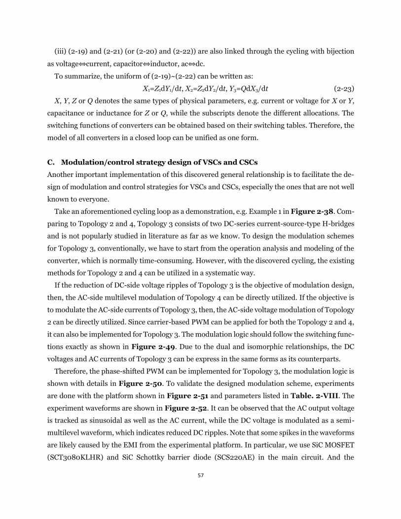
57
(iii) (2-19) and (2-21) (or (2-20) and (2-22)) are also linked through the cycling with bijection
as voltage⇔current, capacitor⇔inductor, ac⇔dc.
To summarize, the uniform of (2-19)~(2-22) can be written as:
X1=Z1dY1/dt, X2=Z2dY2/dt, Y3=QdX3/dt (2-23)
X, Y, Z or Q denotes the same types of physical parameters, e.g. current or voltage for X or Y,
capacitance or inductance for Z or Q, while the subscripts denote the different allocations. The
switching functions of converters can be obtained based on their switching tables. Therefore, the
model of all converters in a closed loop can be unified as one form.
C. Modulation/control strategy design of VSCs and CSCs
Another important implementation of this discovered general relationship is to facilitate the de-
sign of modulation and control strategies for VSCs and CSCs, especially the ones that are not well
known to everyone.
Take an aforementioned cycling loop as a demonstration, e.g. Example 1 in Figure 2-38. Com-
paring to Topology 2 and 4, Topology 3 consists of two DC-series current-source-type H-bridges
and is not popularly studied in literature as far as we know. To design the modulation schemes
for Topology 3, conventionally, we have to start from the operation analysis and modeling of the
converter, which is normally time-consuming. However, with the discovered cycling, the existing
methods for Topology 2 and 4 can be utilized in a systematic way.
If the reduction of DC-side voltage ripples of Topology 3 is the objective of modulation design,
then, the AC-side multilevel modulation of Topology 4 can be directly utilized. If the objective is
to modulate the AC-side currents of Topology 3, then, the AC-side voltage modulation of Topology
2 can be directly utilized. Since carrier-based PWM can be applied for both the Topology 2 and 4,
it can also be implemented for Topology 3. The modulation logic should follow the switching func-
tions exactly as shown in Figure 2-49. Due to the dual and isomorphic relationships, the DC
voltages and AC currents of Topology 3 can be express in the same forms as its counterparts.
Therefore, the phase-shifted PWM can be implemented for Topology 3, the modulation logic is
shown with details in Figure 2-50. To validate the designed modulation scheme, experiments
are done with the platform shown in Figure 2-51 and parameters listed in Table. 2-VIII. The
experiment waveforms are shown in Figure 2-52. It can be observed that the AC output voltage
is tracked as sinusoidal as well as the AC current, while the DC voltage is modulated as a semi-
multilevel waveform, which indicates reduced DC ripples. Note that some spikes in the waveforms
are likely caused by the EMI from the experimental platform. In particular, we use SiC MOSFET
(SCT3080KLHR) and SiC Schottky barrier diode (SCS220AE) in the main circuit. And the
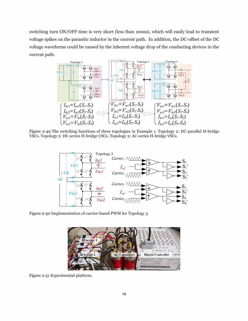
58
switching turn ON/OFF time is very short (less than 100ns), which will easily lead to transient
voltage spikes on the parasitic inductor in the current path. In addition, the DC-offset of the DC
voltage waveforms could be caused by the inherent voltage drop of the conducting devices in the
current path.
Topology 2 Topology 4Topology 3
S1 S2
S3 S4
S1
S2
S3
S4
S1 S2
S3 S4
Vdc1
Vdc2
Iac1
Iac2
Idc
VdcVac1
Vac2
Vdc1
Vac1
Vac2
Vdc2
Vac
S1' S2'
S3' S4'
S1'
S2'
S3'
S4'
S1' S2'
S3' S4'
IdcIac1
Iac2
Vac1=Vdc1(S1-S2)Vac2=Vdc2(S3-S4)
Iac
Idc1
Idc2
Vdc
Vdc1=Vac1(S1-S2)Vdc2=Vac2(S3-S4)
Idc1
Idc2
Idc1=Iac1(S1-S2)Idc2=Iac2(S3-S4)
Iac1=Idc(S1-S2)Iac2=Idc(S3-S4)
Idc1=Iac(S1-S2)Idc2=Iac(S3-S4)
Vac1=Vdc(S1-S2)Vac2=Vdc(S3-S4)
Figure 2-49 The switching functions of three topologies in Example 1. Topology 2: DC-parallel H-bridge VSCs. Topology 2: DC-series H-bridge CSCs. Topology 2: AC-series H-bridge VSCs.
Topology 3S1
S2
S3
S4
Iac1
Iac2
Idc
Vdc1
Vac1
Vac2
Vdc2
S1'
S2'
S3'
S4'
VdcIref
+-Carrier1 S1
-+S1'S2
S2'
Iref +- S3
-+S3'S4
S4'
Carrier2
Carrier3
Carrier4
Figure 2-50 Implementation of carrier-based PWM for Topology 3.
Figure 2-51 Experimental platform.
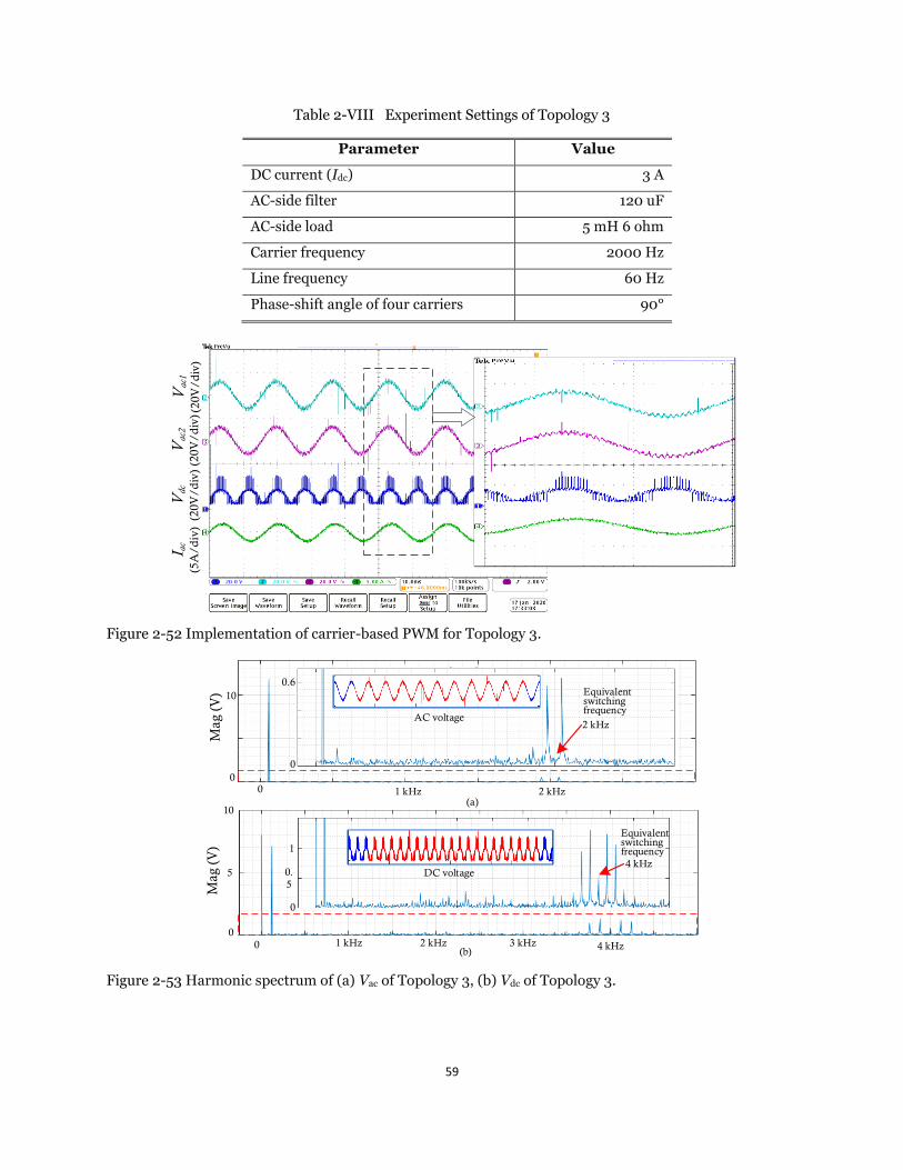
59
Table 2-VIII Experiment Settings of Topology 3
Parameter Value
DC current (Idc) 3 A
AC-side filter 120 uF
AC-side load 5 mH 6 ohm
Carrier frequency 2000 Hz
Line frequency 60 Hz
Phase-shift angle of four carriers 90°
Va
c1
(20V
/div
)V
ac2
(20V
/div
)V
dc
(20V
/div
)I a
c (5
A/d
iv)
Figure 2-52 Implementation of carrier-based PWM for Topology 3.
Mag
(V
)
0 2 kHz1 kHz0
10
2 kHz
0
0.6
0 4 kHz1 kHz0
5
(a)
(b)
10
2 kHz 3 kHz
0
1
0.5
4 kHz
AC voltage
DC voltage
Equivalent switching frequency
Equivalent switching frequency
Mag
(V
)
Figure 2-53 Harmonic spectrum of (a) Vac of Topology 3, (b) Vdc of Topology 3.
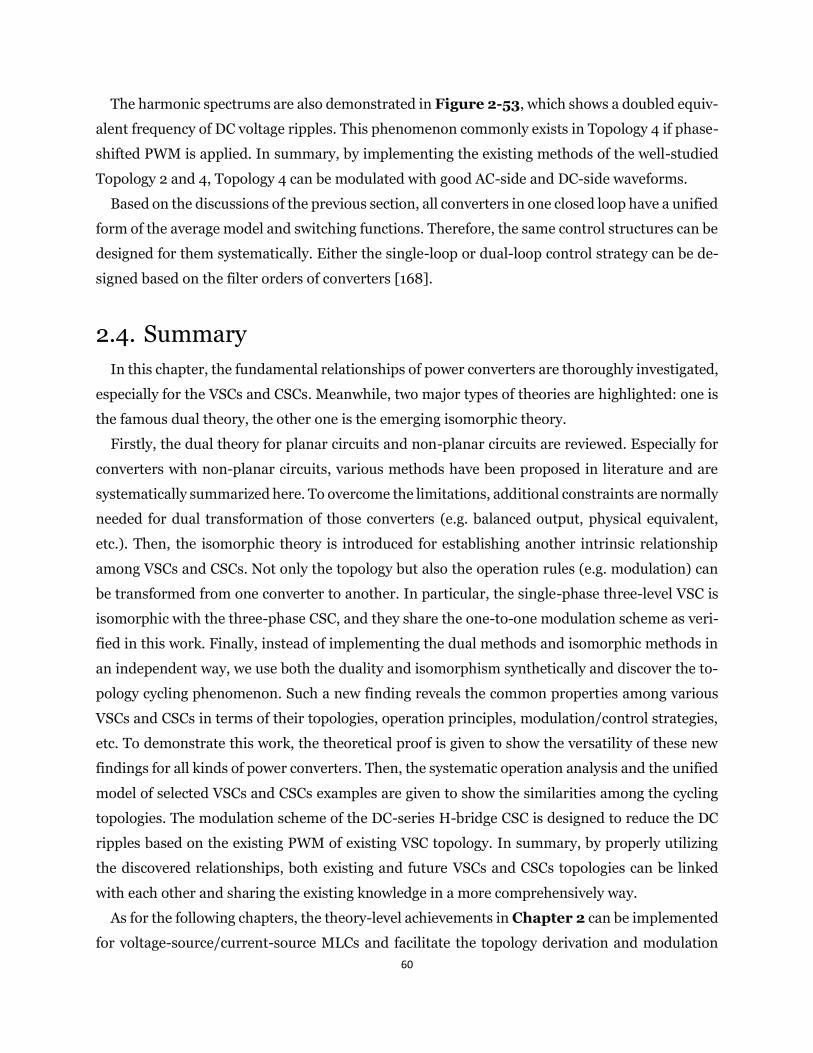
60
The harmonic spectrums are also demonstrated in Figure 2-53, which shows a doubled equiv-
alent frequency of DC voltage ripples. This phenomenon commonly exists in Topology 4 if phase-
shifted PWM is applied. In summary, by implementing the existing methods of the well-studied
Topology 2 and 4, Topology 4 can be modulated with good AC-side and DC-side waveforms.
Based on the discussions of the previous section, all converters in one closed loop have a unified
form of the average model and switching functions. Therefore, the same control structures can be
designed for them systematically. Either the single-loop or dual-loop control strategy can be de-
signed based on the filter orders of converters [168].
2.4. Summary
In this chapter, the fundamental relationships of power converters are thoroughly investigated,
especially for the VSCs and CSCs. Meanwhile, two major types of theories are highlighted: one is
the famous dual theory, the other one is the emerging isomorphic theory.
Firstly, the dual theory for planar circuits and non-planar circuits are reviewed. Especially for
converters with non-planar circuits, various methods have been proposed in literature and are
systematically summarized here. To overcome the limitations, additional constraints are normally
needed for dual transformation of those converters (e.g. balanced output, physical equivalent,
etc.). Then, the isomorphic theory is introduced for establishing another intrinsic relationship
among VSCs and CSCs. Not only the topology but also the operation rules (e.g. modulation) can
be transformed from one converter to another. In particular, the single-phase three-level VSC is
isomorphic with the three-phase CSC, and they share the one-to-one modulation scheme as veri-
fied in this work. Finally, instead of implementing the dual methods and isomorphic methods in
an independent way, we use both the duality and isomorphism synthetically and discover the to-
pology cycling phenomenon. Such a new finding reveals the common properties among various
VSCs and CSCs in terms of their topologies, operation principles, modulation/control strategies,
etc. To demonstrate this work, the theoretical proof is given to show the versatility of these new
findings for all kinds of power converters. Then, the systematic operation analysis and the unified
model of selected VSCs and CSCs examples are given to show the similarities among the cycling
topologies. The modulation scheme of the DC-series H-bridge CSC is designed to reduce the DC
ripples based on the existing PWM of existing VSC topology. In summary, by properly utilizing
the discovered relationships, both existing and future VSCs and CSCs topologies can be linked
with each other and sharing the existing knowledge in a more comprehensively way.
As for the following chapters, the theory-level achievements in Chapter 2 can be implemented
for voltage-source/current-source MLCs and facilitate the topology derivation and modulation

61
design in a systematic way. In Chapter 3, the fundamental relationships in a structure level of
the MLCs will be investigated, e.g. duality, resulting in the unified matrix models of the MLCs that
will be applied for systematic topology derivations for voltage-source/current-source MLC topol-
ogies. Then, the cycling rules can be utilized for generating more new derivations by generalizing
the derived VSC or CSC topology into more circuit forms.
62
Chapter 3 Systematic derivation of multilevel
converters1
In conventional ways, MLCs derivations are mainly realized through circuit-level synthesis (e.g.
voltage-source MLCs) or dual transformation (e.g. current-source MLCs). To derive current-
source MLCs, dual principles are normally utilized to facilitate the topological derivation process
[81], [82], [169]. In [81], the duality principle is utilized to construct the current-source MLCs
topologies based on the existent voltage-source MLCs topologies. In [82], such duality principle
is utilized for MMC derivation considering both the sub-modules and cell connections. However,
these methods tend to be quite complicated when dealing with high-level/non-planar circuits. In
this chapter, we establish the unified models of MLCs based on the structure-level fundamental
relationships extended from Chapter 2. And develop the systematic topology derivation ap-
proach for three types of MLCs (voltage-source, current-source, matrix type).
As introduced in Chapter 2, the duality can be adopted for revealing such relationships in a
higher-level abstract way. For voltage-source MLCs and current-source MLCs, dual relationships
can be found in a structure-level by representing in matrix models. It will be demonstrated that
both types of MLCs can be modeled in stage-based common structures. Therefore, it is possible
to derive these two types of MLCs in a structure-level by following a universal approach. As for
each stage, the basic circuit forms are summarized and can be directly utilized for topology syn-
thesis without conducting dual transformation. Moreover, it is well established that matrix-type
MLCs have the equivalent circuits with voltage-source and current-source MLCs, which can be
considered as another structure-level relationships. Therefore, the matrix-type of MLCs can be
synthesized by directly combining voltage-source and current-source MLCs. In addition, to fur-
ther generalize the derived topology database, the discovered cycling rules can be utilized here.
Once an original topology is derived, it can be transformed into another one/three forms with
clear fundamental relationships (as established in Chapter 2).
1 Publication out of this Chapter:
Yuzhuo Li, Yunwei Li and Zhongyi Quan, "Systematic Synthesis and Derivation of Multilevel Converters Using Common Topological Structures with Unified Matrix Models," in IEEE Transactions on Power Electronics, vol. 35, no. 6, pp. 5639-5659, June 2020. Yuzhuo Li, Nie Hou, Li Ding and Yunwei Li, "Unfolder Operation and Modulation Strategy of Paralleled Current-Source Converters," 2019 IEEE Energy Conversion Congress and Exposition (ECCE), Baltimore, MD, USA, 2019, pp. 5089-5095.
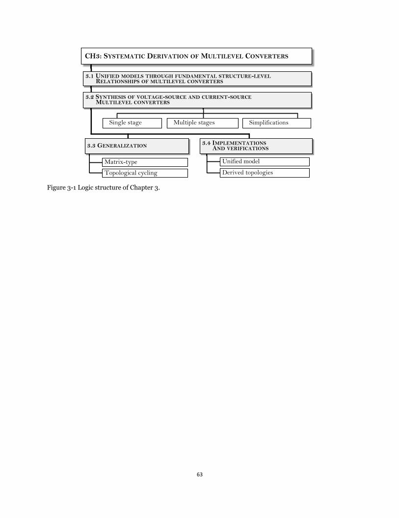
63
Unified model
Derived topologies
3.2 SYNTHESIS OF VOLTAGE-SOURCE AND CURRENT-SOURCE MULTILEVEL CONVERTERS
CH3: SYSTEMATIC DERIVATION OF MULTILEVEL CONVERTERS
3.1 UNIFIED MODELS THROUGH FUNDAMENTAL STRUCTURE-LEVEL RELATIONSHIPS OF MULTILEVEL CONVERTERS
3.3 GENERALIZATION 3.4 IMPLEMENTATIONS AND VERIFICATIONS
Matrix-type
Topological cycling
Single stage Multiple stages Simplifications
Figure 3-1 Logic structure of Chapter 3.
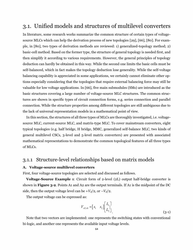
64
3.1. Unified models and structures of multilevel converters
In literature, some research works summarize the common structure of certain types of voltage-
source MLCs which can help the derivation process of new topologies [29], [66], [80]. For exam-
ple, in [80], two types of derivation methods are reviewed: 1) generalized-topology method; 2)
basic-cell method. Based on the former type, the structure of general topology is needed first, and
then simplify it according to various requirements. However, the general principles of topology
deduction can hardly be obtained in this way. While the second one limits the basic cells must be
self-balanced, which in fact makes the topology deduction lose generality. While the self-voltage
balancing capability is appreciated in some applications, we certainly cannot eliminate other op-
tions especially considering that the topologies that require external balancing force may still be
valuable for low voltage applications. In [66], five main submodules (SMs) are introduced as the
basic structures covering a large number of voltage-source MLC structures. The common struc-
tures are shown in specific types of circuit connection forms, e.g. series connection and parallel
connection. While the structure properties among different topologies are still ambiguous due to
the lack of universal representation models in a mathematical point of view.
In this section, the structures of all three types of MLCs are thoroughly investigated, i.e. voltage-
source MLC, current-source MLC, and matrix-type MLC. To cover mainstream converters, eight
typical topologies (e.g. half bridge, H bridge, MMC, generalized self-balance MLC, two kinds of
general multilevel CSCs, 3-level and 5-level matrix converters) are presented with associated
mathematical representations to demonstrate the common topological features of all three types
of MLCs.
3.1.1 Structure-level relationships based on matrix models
A. Voltage-source multilevel converters
First, four voltage-source topologies are selected and discussed as follows.
Voltage-Source Example 1: Circuit form of 2-level (2L) output half-bridge converter is
shown in Figure 3-2. Points A1 and A2 are the output terminals. If A1 is the midpoint of the DC
side, then the output voltage level can be +Vd/2, or −Vd/2.
The output voltage can be expressed as:
12 1 1 2
2A A
LV s s
L
= . (3-1)
Note that two vectors are implemented: one represents the switching states with conventional
bi-logic, and another one represents the available input voltage levels.
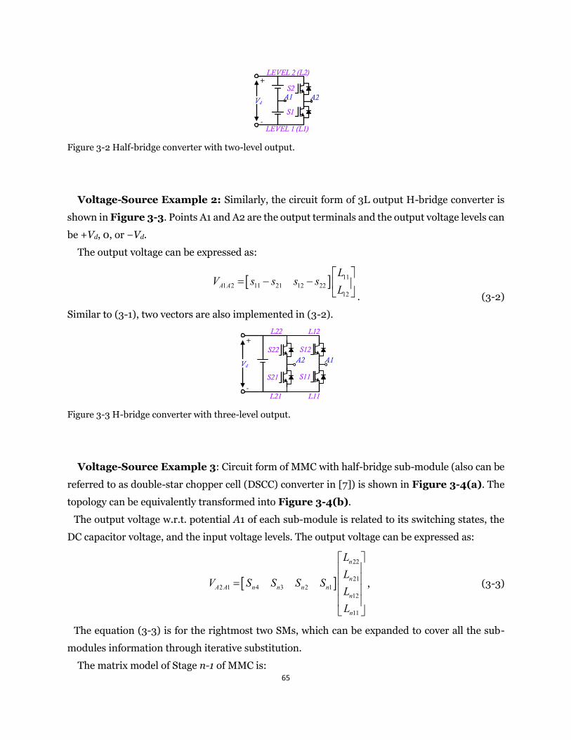
65
Vd
+
-
A2
S2
S1
LEVEL 2 (L2)
LEVEL 1 (L1)
A1
Figure 3-2 Half-bridge converter with two-level output.
Voltage-Source Example 2: Similarly, the circuit form of 3L output H-bridge converter is
shown in Figure 3-3. Points A1 and A2 are the output terminals and the output voltage levels can
be +Vd, 0, or −Vd.
The output voltage can be expressed as:
111 2 11 21 12 22
12A A
LV s s s s
L
= − − . (3-2)
Similar to (3-1), two vectors are also implemented in (3-2).
Vd
+
-
A1
S12
S11
S22
S21
A2
L22
L21
L12
L11
Figure 3-3 H-bridge converter with three-level output.
Voltage-Source Example 3: Circuit form of MMC with half-bridge sub-module (also can be
referred to as double-star chopper cell (DSCC) converter in [7]) is shown in Figure 3-4(a). The
topology can be equivalently transformed into Figure 3-4(b).
The output voltage w.r.t. potential A1 of each sub-module is related to its switching states, the
DC capacitor voltage, and the input voltage levels. The output voltage can be expressed as:
22
212 1 4 3 2 1
12
11
n
nA A n n n n
n
n
LL
V S S S SLL
=
, (3-3)
The equation (3-3) is for the rightmost two SMs, which can be expanded to cover all the sub-
modules information through iterative substitution.
The matrix model of Stage n-1 of MMC is:
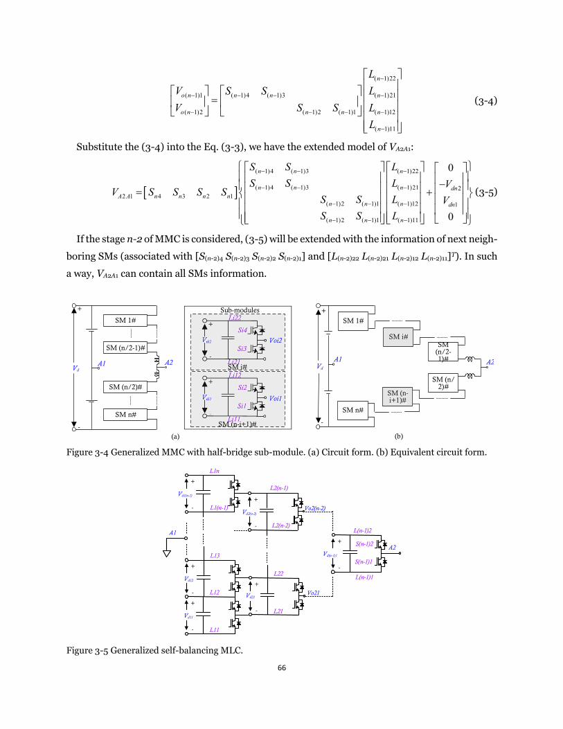
66
( 1)22
( 1)1 ( 1)4 ( 1)3 ( 1)21
( 1)2 ( 1)2 ( 1)1 ( 1)12
( 1)11
n
o n n n n
o n n n n
n
LV S S LV S S L
L
−
− − − −
− − − −
−
=
(3-4)
Substitute the (3-4) into the Eq. (3-3), we have the extended model of VA2A1:
( 1)4 ( 1)3 ( 1)22
( 1)4 ( 1)3 ( 1)21 22 1 4 3 2 1
( 1)2 ( 1)1 ( 1)12 1
( 1)2 ( 1)1 ( 1)11
0
0
n n n
n n n dnA A n n n n
n n n dn
n n n
S S LS S L V
V S S S SS S L VS S L
− − −
− − −
− − −
− − −
− = +
(3-5)
If the stage n-2 of MMC is considered, (3-5) will be extended with the information of next neigh-
boring SMs (associated with [S(n-2)4 S(n-2)3 S(n-2)2 S(n-2)1] and [L(n-2)22 L(n-2)21 L(n-2)12 L(n-2)11]T). In such
a way, VA2A1 can contain all SMs information.
SM 1#
SM (n/2-1)#
SM (n/2)#
SM n#
Vd
+
-
A2A1
Vdi2
+
-
Voi2Si4
Si3
Li22
Li21
Vdi1
+
-
Si2
Si1
Li12
Li11
Voi1
Sub-modules
Vdi2Vdi2V
+
-
Voi2Si4
Si3
Li22
Li21SM i#
Vdi1Vdi1V
+
-
Si2i2i
Si1
Li12
Li11
Voi1
SM (n-i+1)#
Vd
+
-
SM 1#
SM n#
SM i#SM i#
SM (n-i+1)#SM (n-i+1)#
SM (n/2-1)#
SM (n/2)#
A2A1
(a) (b) Figure 3-4 Generalized MMC with half-bridge sub-module. (a) Circuit form. (b) Equivalent circuit form.
Vd12
+
-
L13
L12
Vd11
+
- L11
L1n
Vd1(n-1)
+
- L1(n-1)
A1
L2(n-1)
Vd2(n-2)
+
- L2(n-2)
Vo2(n-2)
L22
+
- L21
Vo21Vd21
L(n-1)2
Vd(n-1)1
+
-
L(n-1)1
S(n-1)2
S(n-1)1
A2
Figure 3-5 Generalized self-balancing MLC.
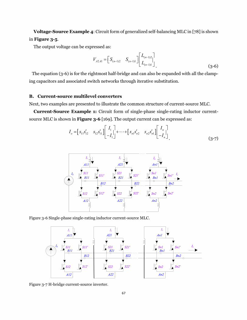
67
Voltage-Source Example 4: Circuit form of generalized self-balancing MLC in [78] is shown
in Figure 3-5.
The output voltage can be expressed as:
( 1)22 1 ( 1)2 ( 1)1
( 1)1
nA A n n
n
LV S S
L−
− −
−
=
. (3-6)
The equation (3-6) is for the rightmost half-bridge and can also be expanded with all the clamp-
ing capacitors and associated switch networks through iterative substitution.
B. Current-source multilevel converters
Next, two examples are presented to illustrate the common structure of current-source MLC.
Current-Source Example 1: Circuit form of single-phase single-rating inductor current-
source MLC is shown in Figure 3-6 [169]. The output current can be expressed as:
111 12 12 11 1 2 2 1
1
no n n n n
n
III s s s s s s s s
II
= + + −− . (3-7)
B12
B11
I1
A11
A12
Id
B22
B21
A21
A22
S11'S11
S12'S12
S21'S21
S22'S22
Bn2
Bn1
An1
An2
Sn1'Sn1
Sn2'Sn2
I2 In
Io
Figure 3-6 Single-phase single-rating inductor current-source MLC.
B12
B11
A11
A12
B22
B21
A21
A22
S11'S11
S12'S12
S21'S21
S22'S22
Bn2
Bn1
An1
An2
Sn1'Sn1
Sn2'Sn2
I1 I2 I3
IoId
Figure 3-7 H-bridge current-source inverter.
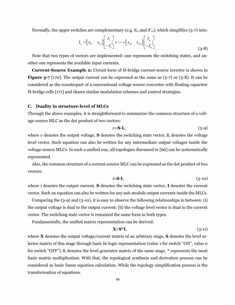
68
Normally, the upper switches are complementary (e.g. S11 and S'11), which simplifies (3-7) into:
111 12 1 2
1
no n n
n
III s s s s
II
= + + −− . (3-8)
Note that two types of vectors are implemented: one represents the switching states, and an-
other one represents the available input currents.
Current-Source Example 2: Circuit form of H-bridge current-source inverter is shown in
Figure 3-7 [170]. The output current can be expressed as the same as (3-7) or (3-8). It can be
considered as the counterpart of a conventional voltage source converter with floating capacitor
H-bridge cells [171] and shares similar modulation schemes and control strategies.
C. Duality in structure-level of MLCs
Through the above examples, it is straightforward to summarize the common structure of a volt-
age-source MLC as the dot product of two vectors:
v=S∙L, (3-9)
where v denotes the output voltage, S denotes the switching state vector, L denotes the voltage
level vector. Such equation can also be written for any intermediate output voltages inside the
voltage-source MLCs. In such a unified way, all topologies discussed in [66] can be systematically
represented.
Also, the common structure of a current-source MLC can be expressed as the dot product of two
vectors:
i=S∙I, (3-10)
where i denotes the output current, S denotes the switching state vector, I denotes the current
vector. Such an equation can also be written for any sub-module output currents inside the MLCs.
Comparing the (3-9) and (3-10), it is easy to observe the following relationships in between: (i)
the output voltage is dual to the output current; (ii) the voltage level vector is dual to the current
vector. The switching state vector is remained the same form in both types.
Fundamentally, the unified matrix representation can be derived:
X=S*L (3-11)
where X denotes the output voltage/current matrix of an arbitrary stage, S denotes the level se-
lector matrix of this stage through basic bi-logic representation (value 1 for switch “ON”, value 0
for switch “OFF”), L denotes the level generator matrix of the same stage, * represents the most
basic matrix multiplication. With that, the topological synthesis and derivation process can be
considered as basic linear equation calculation. While the topology simplification process is the
transformation of equations.
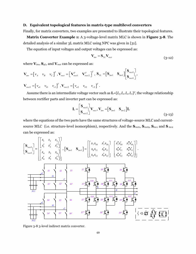
69
D. Equivalent topological features in matrix-type multilevel converters
Finally, for matrix converters, two examples are presented to illustrate their topological features.
Matrix Converter Example 1: A 3-voltage-level matrix MLC is shown in Figure 3-8. The
detailed analysis of a similar 3L matrix MLC using NPC was given in [31].
The equation of input voltages and output voltages can be expressed as:
3inv L rect=V S V (3-12)
where Vinv, S3L, and Vrect can be expressed as:
1 2,TT T T
inv A B C rect rect rectv v v = = V V V V , 13 1 1
1
rectL inv inv
rect
=
SS S S
S,
1 1 1 1 2 2 2 2,T Trect a b c rect a b cv v v v v v= =V V .
Assume there is an intermediate voltage vector such as L=[L3 L2 L2 L1]T, the voltage relationship
between rectifier parts and inverter part can be expressed as:
11 2
2
,rectrect inv inv inv
rect
= =
SL V V S S L
S (3-13)
where the equations of the two parts have the same structures of voltage-source MLC and current-
source MLC (i.e. structure-level isomorphism), respectively. And the Srect1, Srect2, Sinv1 and S inv2
can be expressed as:
1 2 3
1 2 31
1 4 5 6
4 5 6
rect
rect
s s ss s s
s s ss s s
=
SS
, 7 10 7 10 7 10 7 10
1 1 8 11 8 11 8 11 8 11
9 12 9 12 9 12 9 12
inv inv
s s s s s s s ss s s s s s s ss s s s s s s s
=
S S .
b1a1
c1
BA
CN11
b2a2
c2
N12
S1'
S1
S2'
S2 S3
S3' S7'
S7
S4'
S4
S5'
S5 S6
S6'
S7''
S7'''
S8'
S8
S8''
S8'''
S9'
S9
S9''
S9'''
S10'
S10
S11'
S11
S12'
S12
Figure 3-8 3-level indirect matrix converter.
70
Matrix Converter Example 2: A 5-current-level matrix MLC is demonstrated in Figure 3-
9. Note that this topology is parallel indirect matrix converters system as described in [172].
The equation of input currents and output currents can be expressed as:
5T
rect L inv=I S I (3-14)
where Iinv, S5L, and Irect can be expressed as:
1 2 1 1 1 1 2 2 2 2, ,T T TT T
inv inv inv inv A B C inv A B Ci i i i i i = = = I I I I I ,
1 2 1 1 1 1 2 2 2 2, ,T T TT T
rect rect rect rect a b c rect a b ci i i i i i = = = I I I I I ,
1 15
2 2
inv rectL
inv rect
=
S SS
S S,
7 7 10 10
1 8 8 1 11 11
9 9 12 12
,inv inv
s s s ss s s ss s s s
= =
S S ,
1 2 3 4 5 61 2
1 2 3 4 5 6
,rect rect
s s s s s ss s s s s s
= = S S .
Assume the intermediate current vector is L=[L1 −L1 L2 −L2]T, the current relationship between
rectifier parts and inverter part can be expressed as:
1
2
TTrect
rect Trect
=
SI L
S,
1
2
TTinv
invTinv
=
SL I
S, (3-15)
which has the same structure of current-source MLC (i.e. structure-level equivalence).
N2Load or source
a2b2c2
a1b1c1
abc
AB
C
S1'
S1
S2'
S2 S3
S3' S7'
S7
S4'
S4
S5'
S5 S6
S6'
S8'
S8
S9'
S9
S10'
S10
S11'
S11
S12'
S12
Figure 3-9 Indirect matrix converter with 5L current output.
71
This section investigates the common structures among all three kinds of MLCs with associated
matrix representations. It is demonstrated that the outputs of MLCs can be represented in a
unique dot product of two matrices. For complex circuits, the models can be developed iteratively.
In such way, the similarity and difference of various MLCs can be exhibited in a mathematical
way, and the derivation method for one topology can be mathematically transformed into another
one which will greatly facilitate the derivation process.
3.1.2 Stage-based structures of multilevel converters
In literature, similar concepts towards the MLC structure have been developed e.g. level lines,
layers [78]-[80], [173]which easily leads to confusions under different semantics towards differ-
ent types of topologies. Based on the summary of common structures of MLC topologies in the
previous section, all three types of MLCs can be represented in a unified mathematical form. In
this section, such a concept is defined more precisely and will be discussed thoroughly with
demonstration examples to help better understand the mathematical models and the topological
relationships of various MLC topologies.
To represent voltage-source and current-source MLC in a generalized manner, the concept of
the stage is introduced in this section. In the proposed concept, a multilevel topology is composed
of several stages, as shown in Figure 3-10. Herein a voltage-source MLC or a current-source
MLC is considered as a composition of several consecutively connected stages as shown in Figure
3-10(a) and (b). Each stage can have single or multiple inputs and single or multiple outputs
with different circuit appearance. A stage can be further decomposed into a combination of level
generators (LGs) and level selectors (LSs). An LG is a circuit responsible for generating or retain-
ing the desired voltage/current levels. An LS is a circuit responsible for selecting the proper volt-
age/current levels that generated from the previous LG. The typical structure of a stage is com-
posed of an LG and an LS. Since selecting level within each stage is actually based on modulation
strategy, both high and low-frequency behavior can be represented in the proposed concept.
A matrix MLC can be considered as a combination of voltage-source MLC with a virtual voltage
source and current-source MLC with a virtual current source. Furthermore, the physical switches
are abstracted into the node-branch diagram. The topology synthesis and derivation are realized
by designing and manipulating the stages with node-branch diagram.
The stage-based common structure of MLC with shared DC link shows that a stage has a com-
plete voltage/current level output capability, which can be considered as the smallest unit of func-
tional circuits in a topology. Two-level topologies can be considered special cases from the stage-
based point of view.
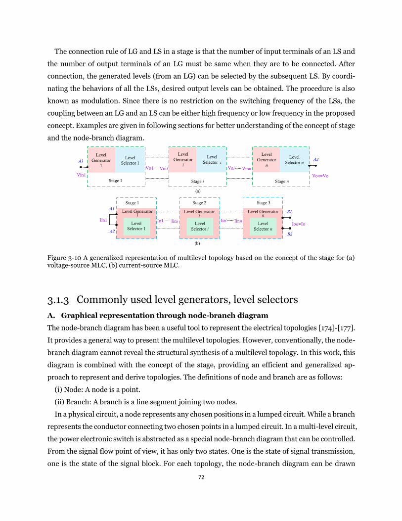
72
The connection rule of LG and LS in a stage is that the number of input terminals of an LS and
the number of output terminals of an LG must be same when they are to be connected. After
connection, the generated levels (from an LG) can be selected by the subsequent LS. By coordi-
nating the behaviors of all the LSs, desired output levels can be obtained. The procedure is also
known as modulation. Since there is no restriction on the switching frequency of the LSs, the
coupling between an LG and an LS can be either high frequency or low frequency in the proposed
concept. Examples are given in following sections for better understanding of the concept of stage
and the node-branch diagram.
Level Generator 1
Stage 1 Stage 2 Stage 3
B1
B2
Level Selector 1
Level Generator i
Level Selector i
Level Generator n
LevelSelector n
Io1 Iini Ioi IinnIon=Io
Iin1
A1
A2
Level Generator
1A1
Level Selector 1
Stage iStage 1 Stage n
A2
Von=Vo
Level Generator
i
LevelSelector i
Level Generator
n
LevelSelector n
Vo1 VoiVini VinnVin1
(a)
(b) Figure 3-10 A generalized representation of multilevel topology based on the concept of the stage for (a) voltage-source MLC, (b) current-source MLC.
3.1.3 Commonly used level generators, level selectors
A. Graphical representation through node-branch diagram
The node-branch diagram has been a useful tool to represent the electrical topologies [174]-[177].
It provides a general way to present the multilevel topologies. However, conventionally, the node-
branch diagram cannot reveal the structural synthesis of a multilevel topology. In this work, this
diagram is combined with the concept of the stage, providing an efficient and generalized ap-
proach to represent and derive topologies. The definitions of node and branch are as follows:
(i) Node: A node is a point.
(ii) Branch: A branch is a line segment joining two nodes.
In a physical circuit, a node represents any chosen positions in a lumped circuit. While a branch
represents the conductor connecting two chosen points in a lumped circuit. In a multi-level circuit,
the power electronic switch is abstracted as a special node-branch diagram that can be controlled.
From the signal flow point of view, it has only two states. One is the state of signal transmission,
one is the state of the signal block. For each topology, the node-branch diagram can be drawn
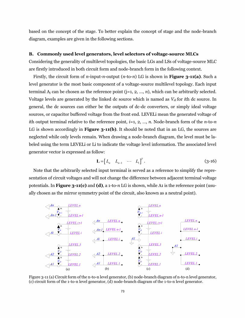
73
based on the concept of the stage. To better explain the concept of stage and the node-branch
diagram, examples are given in the following sections.
B. Commonly used level generators, level selectors of voltage-source MLCs
Considering the generality of multilevel topologies, the basic LGs and LSs of voltage-source MLC
are firstly introduced in both circuit form and node-branch form in the following context.
Firstly, the circuit form of n-input-n-output (n-to-n) LG is shown in Figure 3-11(a). Such a
level generator is the most basic component of a voltage-source multilevel topology. Each input
terminal Aj can be chosen as the reference point (j=1, 2, …, n), which can be arbitrarily selected.
Voltage levels are generated by the linked dc source which is named as Vdi for ith dc source. In
general, the dc sources can either be the outputs of dc-dc converters, or simply ideal voltage
sources, or capacitor buffered voltage from the front end. LEVELi mean the generated voltage of
ith output terminal relative to the reference point, i=1, 2, …, n. Node-branch form of the n-to-n
LG is shown accordingly in Figure 3-11(b). It should be noted that in an LG, the sources are
neglected while only levels remain. When drawing a node-branch diagram, the level must be la-
beled using the term LEVELi or Li to indicate the voltage level information. The associated level
generator vector is expressed as follow:
1 1T
n nL L L−=L . (3-16)
Note that the arbitrarily selected input terminal is served as a reference to simplify the repre-
sentation of circuit voltages and will not change the difference between adjacent terminal voltage
potentials. In Figure 3-11(c) and (d), a 1-to-n LG is shown, while A1 is the reference point (usu-
ally chosen as the mirror symmetry point of the circuit, also known as a neutral point).
Vd2
+
-
LEVEL 3
LEVEL 2
Vd1
+
- LEVEL 1
LEVEL i+1
Vdi
+
- LEVEL i
LEVEL n
Vdn-1
+
- LEVEL n-1
An
An-1
Ai
A1
A2
Ai
LEVEL n
LEVEL n-1
LEVEL 2
LEVEL 1
LEVEL i
An-1
An
A1
A2
(a) (b)
Vd2
+
-
LEVEL 3
LEVEL 2
Vd1
+
- LEVEL 1
LEVEL i+1
Vdi
+
- LEVEL i
LEVEL n
Vdn-1
+
- LEVEL n-1
A1
A1
LEVEL n
LEVEL n-1
LEVEL 2
LEVEL 1
LEVEL i
(c) (d)
Figure 3-11 (a) Circuit form of the n-to-n level generator, (b) node-branch diagram of n-to-n level generator, (c) circuit form of the 1-to-n level generator, (d) node-branch diagram of the 1-to-n level generator.
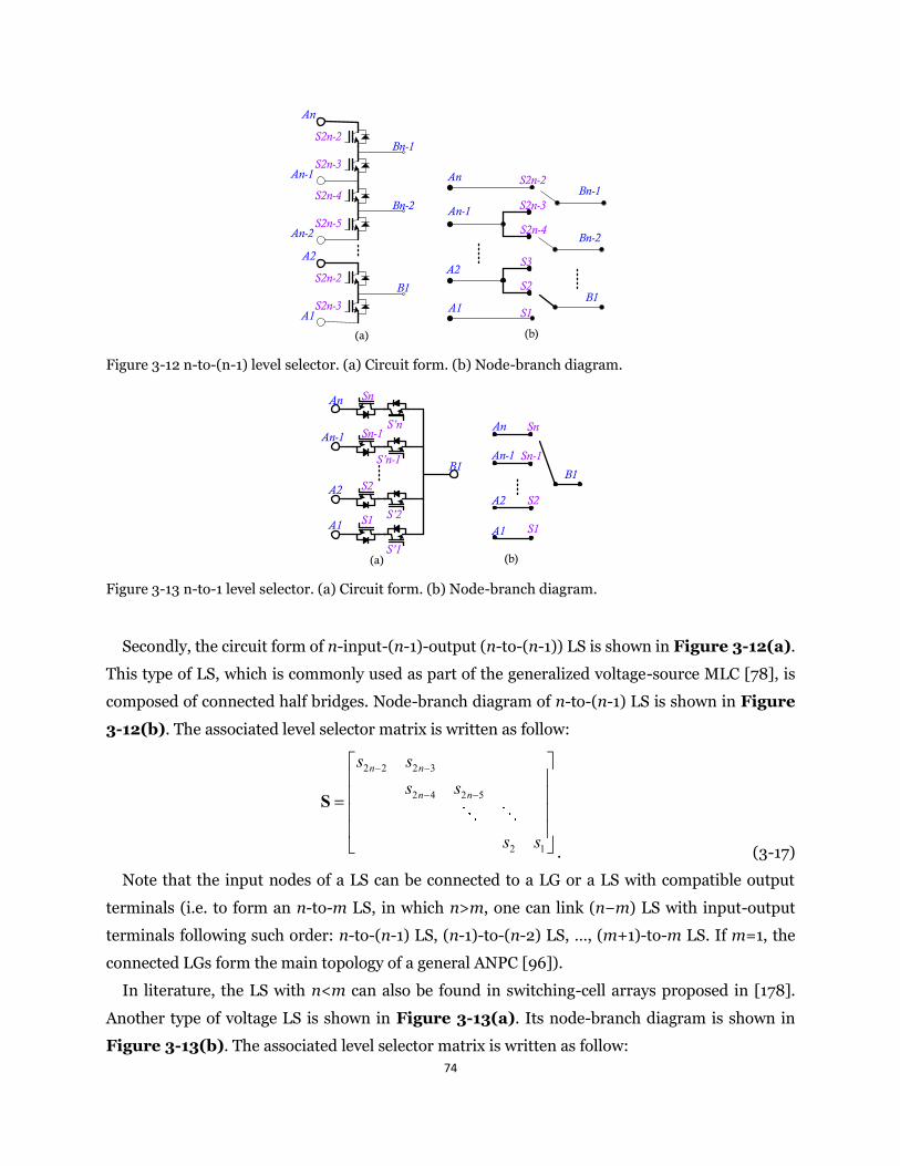
74
Bn-1S2n-2
An
S2n-3An-1
Bn-2S2n-4
S2n-5An-2
B1S2n-2
A2
S2n-3A1
An
A2
An-1
A1
Bn-1
Bn-2
B1
S2n-2
S2n-3
S2n-4
S2
S1
S3
(a) (b)
Figure 3-12 n-to-(n-1) level selector. (a) Circuit form. (b) Node-branch diagram.
An
Sn-1An-1
A2
A1
S n-1
S2
S
B1
Sn
S n
S1
S
A2
An-1
A1
B1
An
Sn-1
S2
Sn
S1
(a) (b)
Figure 3-13 n-to-1 level selector. (a) Circuit form. (b) Node-branch diagram.
Secondly, the circuit form of n-input-(n-1)-output (n-to-(n-1)) LS is shown in Figure 3-12(a).
This type of LS, which is commonly used as part of the generalized voltage-source MLC [78], is
composed of connected half bridges. Node-branch diagram of n-to-(n-1) LS is shown in Figure
3-12(b). The associated level selector matrix is written as follow:
2 2 2 3
2 4 2 5
2 1
n n
n n
s ss s
s s
− −
− −
=
S
. (3-17)
Note that the input nodes of a LS can be connected to a LG or a LS with compatible output
terminals (i.e. to form an n-to-m LS, in which n>m, one can link (n−m) LS with input-output
terminals following such order: n-to-(n-1) LS, (n-1)-to-(n-2) LS, …, (m+1)-to-m LS. If m=1, the
connected LGs form the main topology of a general ANPC [96]).
In literature, the LS with n<m can also be found in switching-cell arrays proposed in [178].
Another type of voltage LS is shown in Figure 3-13(a). Its node-branch diagram is shown in
Figure 3-13(b). The associated level selector matrix is written as follow:
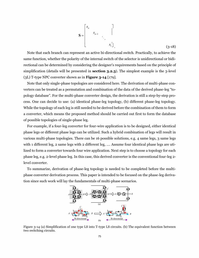
75
1
1
n
n
ss
s
−
=
S
. (3-18)
Note that each branch can represent an active bi-directional switch. Practically, to achieve the
same function, whether the polarity of the internal switch of the selector is unidirectional or bidi-
rectional can be determined by considering the designer's requirements based on the principle of
simplification (details will be presented in section 3.2.3). The simplest example is the 3-level
(3L) T-type NPC converter shown as in Figure 3-14 [179].
Note that only single-phase topologies are considered here. The derivation of multi-phase con-
verters can be treated as a permutation and combination of the data of the derived phase-leg “to-
pology database”. For the multi-phase converter design, the derivation is still a step-by-step pro-
cess. One can decide to use: (a) identical phase-leg topology, (b) different phase-leg topology.
While the topology of each leg is still needed to be derived before the combination of them to form
a converter, which means the proposed method should be carried out first to form the database
of possible topologies of single-phase leg.
For example, if a four-leg converter for four-wire application is to be designed, either identical
phase legs or different phase legs can be utilized. Such a hybrid combination of legs will result in
various multi-phase topologies. There can be 16 possible solutions, e.g. 4 same legs, 3 same legs
with 1 different leg, 2 same legs with 2 different leg, …. Assume four identical phase legs are uti-
lized to form a converter towards four wire application. Next step is to choose a topology for each
phase leg, e.g. 2-level phase leg. In this case, this derived converter is the conventional four-leg 2-
level converter.
To summarize, derivation of phase-leg topology is needed to be completed before the multi-
phase converter derivation process. This paper is intended to be focused on the phase-leg deriva-
tion since such work will lay the fundamentals of multi-phase scenarios.
A
C
B
A
C
B A
C
B
C
BA
C
A
(a)
(b)
B
Bi-directional Bi-directional
Figure 3-14 (a) Simplification of one type LS into T-type LS circuits. (b) The equivalent function between two switching circuits.
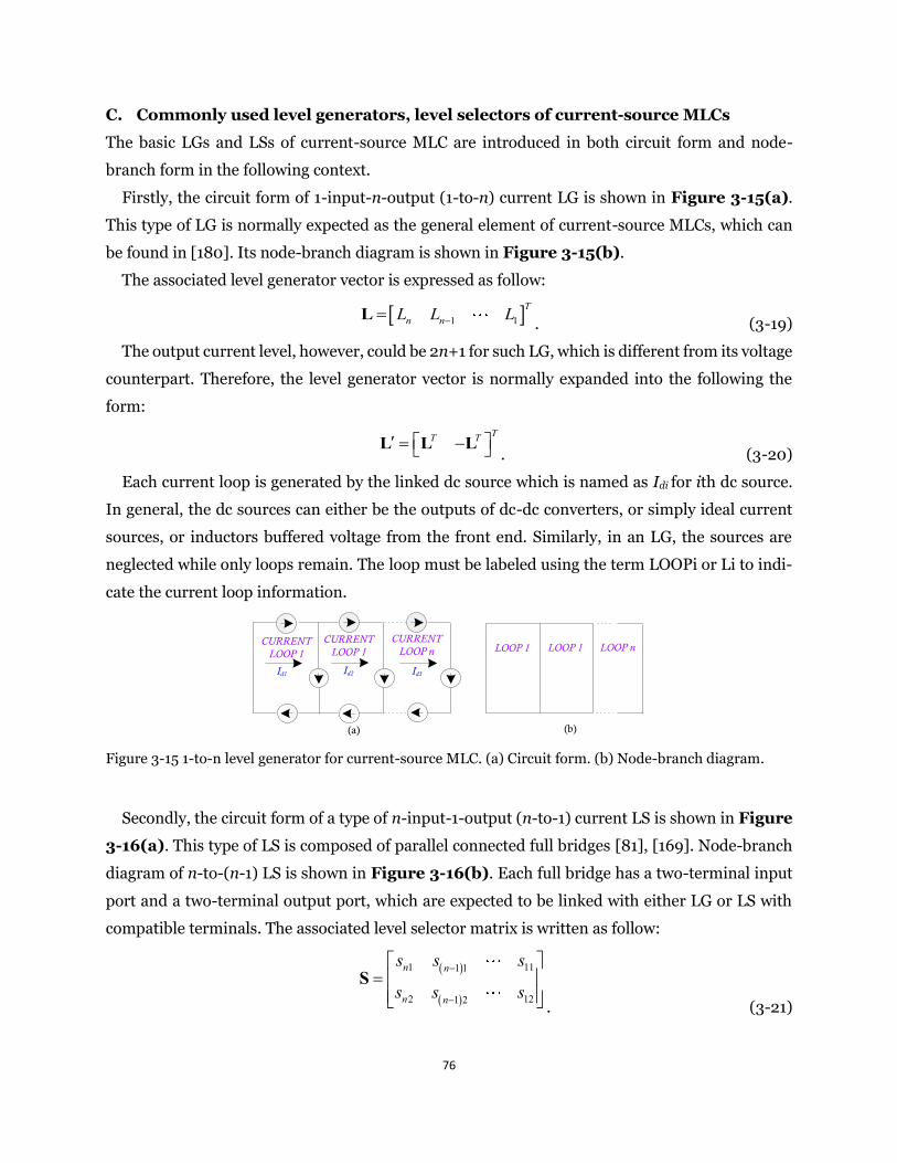
76
C. Commonly used level generators, level selectors of current-source MLCs
The basic LGs and LSs of current-source MLC are introduced in both circuit form and node-
branch form in the following context.
Firstly, the circuit form of 1-input-n-output (1-to-n) current LG is shown in Figure 3-15(a).
This type of LG is normally expected as the general element of current-source MLCs, which can
be found in [180]. Its node-branch diagram is shown in Figure 3-15(b).
The associated level generator vector is expressed as follow:
1 1T
n nL L L−=L. (3-19)
The output current level, however, could be 2n+1 for such LG, which is different from its voltage
counterpart. Therefore, the level generator vector is normally expanded into the following the
form:
TT T = − L L L. (3-20)
Each current loop is generated by the linked dc source which is named as Idi for ith dc source.
In general, the dc sources can either be the outputs of dc-dc converters, or simply ideal current
sources, or inductors buffered voltage from the front end. Similarly, in an LG, the sources are
neglected while only loops remain. The loop must be labeled using the term LOOPi or Li to indi-
cate the current loop information.
CURRENT
LOOP 1
Id1 Id2 Id3
CURRENT
LOOP 1
CURRENT
LOOP n LOOP 1 LOOP 1 LOOP n
(a) (b)
Figure 3-15 1-to-n level generator for current-source MLC. (a) Circuit form. (b) Node-branch diagram.
Secondly, the circuit form of a type of n-input-1-output (n-to-1) current LS is shown in Figure
3-16(a). This type of LS is composed of parallel connected full bridges [81], [169]. Node-branch
diagram of n-to-(n-1) LS is shown in Figure 3-16(b). Each full bridge has a two-terminal input
port and a two-terminal output port, which are expected to be linked with either LG or LS with
compatible terminals. The associated level selector matrix is written as follow:
( )
( )
1 111 1
2 121 2
n n
n n
s s s
s s s−
−
=
S. (3-21)
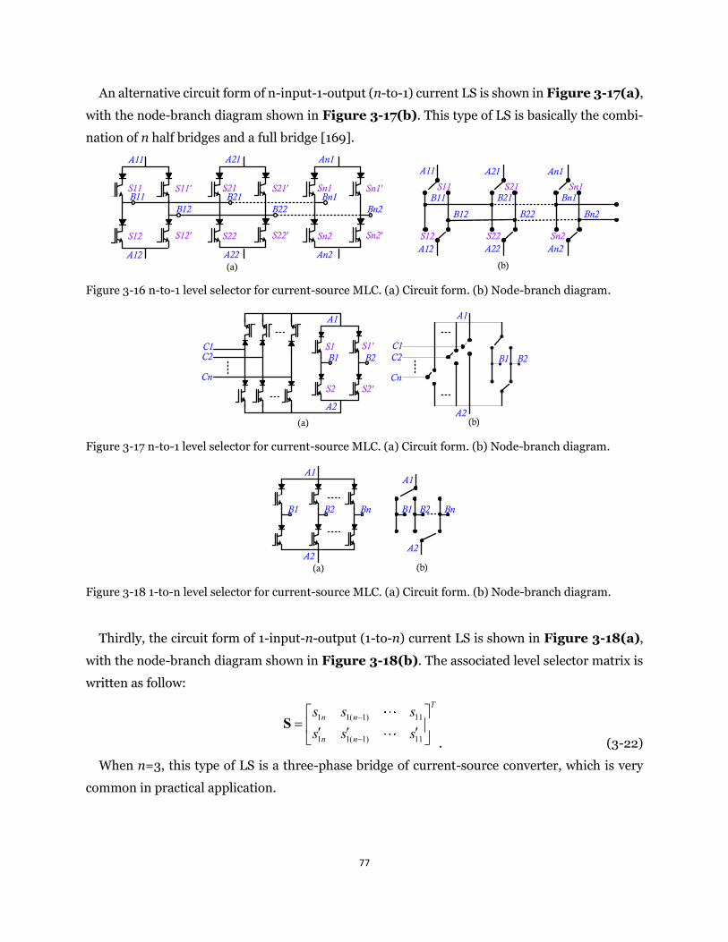
77
An alternative circuit form of n-input-1-output (n-to-1) current LS is shown in Figure 3-17(a),
with the node-branch diagram shown in Figure 3-17(b). This type of LS is basically the combi-
nation of n half bridges and a full bridge [169].
B12
B11
A11
A12
B22
B21
A21
A22
S11'S11
S12'S12
S21'S21
S22'S22
Bn2
Bn1
An1
An2
Sn1'Sn1
Sn2'Sn2
A11
A12
B12
B11
A21
A22
B22
B21S11
S12
S21
S22
An1
An2
Bn2
Bn1Sn1
Sn2
(a) (b)
Figure 3-16 n-to-1 level selector for current-source MLC. (a) Circuit form. (b) Node-branch diagram.
A1
A2
B2B1
C1
C2
Cn
C1C2
Cn
B2B1
A1
A2
S1'S1
S2'S2
(a) (b)
Figure 3-17 n-to-1 level selector for current-source MLC. (a) Circuit form. (b) Node-branch diagram.
B2B1
A1
A2
Bn
A1
A2
BnB1 B2
(a) (b)
Figure 3-18 1-to-n level selector for current-source MLC. (a) Circuit form. (b) Node-branch diagram.
Thirdly, the circuit form of 1-input-n-output (1-to-n) current LS is shown in Figure 3-18(a),
with the node-branch diagram shown in Figure 3-18(b). The associated level selector matrix is
written as follow:
1 1( 1) 11
1 1( 1) 11
Tn n
n n
s s ss s s
−
−
=
S. (3-22)
When n=3, this type of LS is a three-phase bridge of current-source converter, which is very
common in practical application.
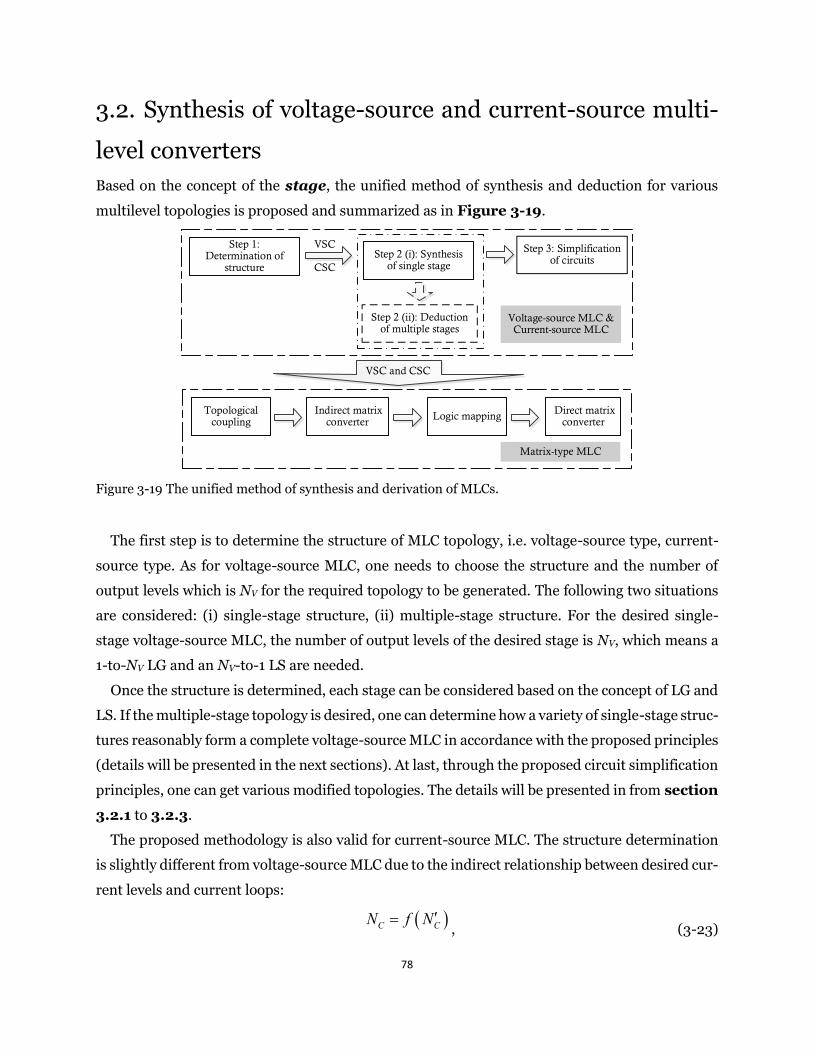
78
3.2. Synthesis of voltage-source and current-source multi-
level converters
Based on the concept of the stage, the unified method of synthesis and deduction for various
multilevel topologies is proposed and summarized as in Figure 3-19.
Step 3: Simplification of circuits
Step 2 (ii): Deduction of multiple stages
Step 2 (i): Synthesis of single stage
Step 1: Determination of
structure
VSC
CSC
Topological coupling
VSC and CSC
Direct matrix converterLogic mapping Indirect matrix
converter
Voltage-source MLC & Current-source MLC
Matrix-type MLC
Figure 3-19 The unified method of synthesis and derivation of MLCs.
The first step is to determine the structure of MLC topology, i.e. voltage-source type, current-
source type. As for voltage-source MLC, one needs to choose the structure and the number of
output levels which is NV for the required topology to be generated. The following two situations
are considered: (i) single-stage structure, (ii) multiple-stage structure. For the desired single-
stage voltage-source MLC, the number of output levels of the desired stage is NV, which means a
1-to-NV LG and an NV-to-1 LS are needed.
Once the structure is determined, each stage can be considered based on the concept of LG and
LS. If the multiple-stage topology is desired, one can determine how a variety of single-stage struc-
tures reasonably form a complete voltage-source MLC in accordance with the proposed principles
(details will be presented in the next sections). At last, through the proposed circuit simplification
principles, one can get various modified topologies. The details will be presented in from section
3.2.1 to 3.2.3.
The proposed methodology is also valid for current-source MLC. The structure determination
is slightly different from voltage-source MLC due to the indirect relationship between desired cur-
rent levels and current loops:
( )C CN f N =, (3-23)
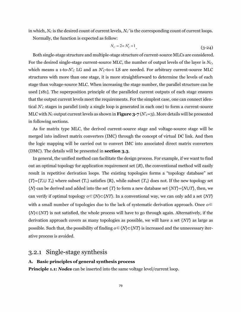
79
in which, NC is the desired count of current levels, NC’ is the corresponding count of current loops.
Normally, the function is expected as follow:
2 1C CN N = + . (3-24)
Both single-stage structure and multiple-stage structure of current-source MLCs are considered.
For the desired single-stage current-source MLC, the number of output levels of the layer is NC,
which means a 1-to-N'C LG and an N'C-to-1 LS are needed. For arbitrary current-source MLC
structures with more than one stage, it is more straightforward to determine the levels of each
stage than voltage-source MLC. When increasing the stage number, the parallel structure can be
used [181]. The superposition principle of the paralleled current outputs of each stage ensures
that the output current levels meet the requirements. For the simplest case, one can connect iden-
tical N'C stages in parallel (only a single loop is generated in each one) to form a current-source
MLC with NC output current levels as shown in Figure 3-7 (N'C=3). More details will be presented
in following sections.
As for matrix type MLC, the derived current-source stage and voltage-source stage will be
merged into indirect matrix converters (IMC) through the concept of virtual DC link. And then
the logic mapping will be carried out to convert IMC into associated direct matrix converters
(DMC). The details will be presented in section 3.3.
In general, the unified method can facilitate the design process. For example, if we want to find
out an optimal topology for application requirement set {R}, the conventional method will easily
result in repetitive derivation loops. The existing topologies forms a “topology database” set
{T}={T1⋃ T2} where subset {T1} satisfies {R}, while subset {T2} does not. If the new topology set
{N} can be derived and added into the set {T} to form a new database set {NT}={N⋃T}, then, we
can verify if optimal topology o∈{N}⊂{NT}. In a conventional way, we can only add a set {NT}
with a small number of topologies due to the lack of systematic derivation approach. Once o∈
{N}⊂{NT} is not satisfied, the whole process will have to go through again. Alternatively, if the
derivation approach covers as many topologies as possible, we will have a set {NT} as large as
possible. Such that, the possibility of finding o∈{N}⊂{NT} is increased and the unnecessary iter-
ative process is avoided.
3.2.1 Single-stage synthesis
A. Basic principles of general synthesis process
Principle 1.1: Nodes can be inserted into the same voltage level/current loop.
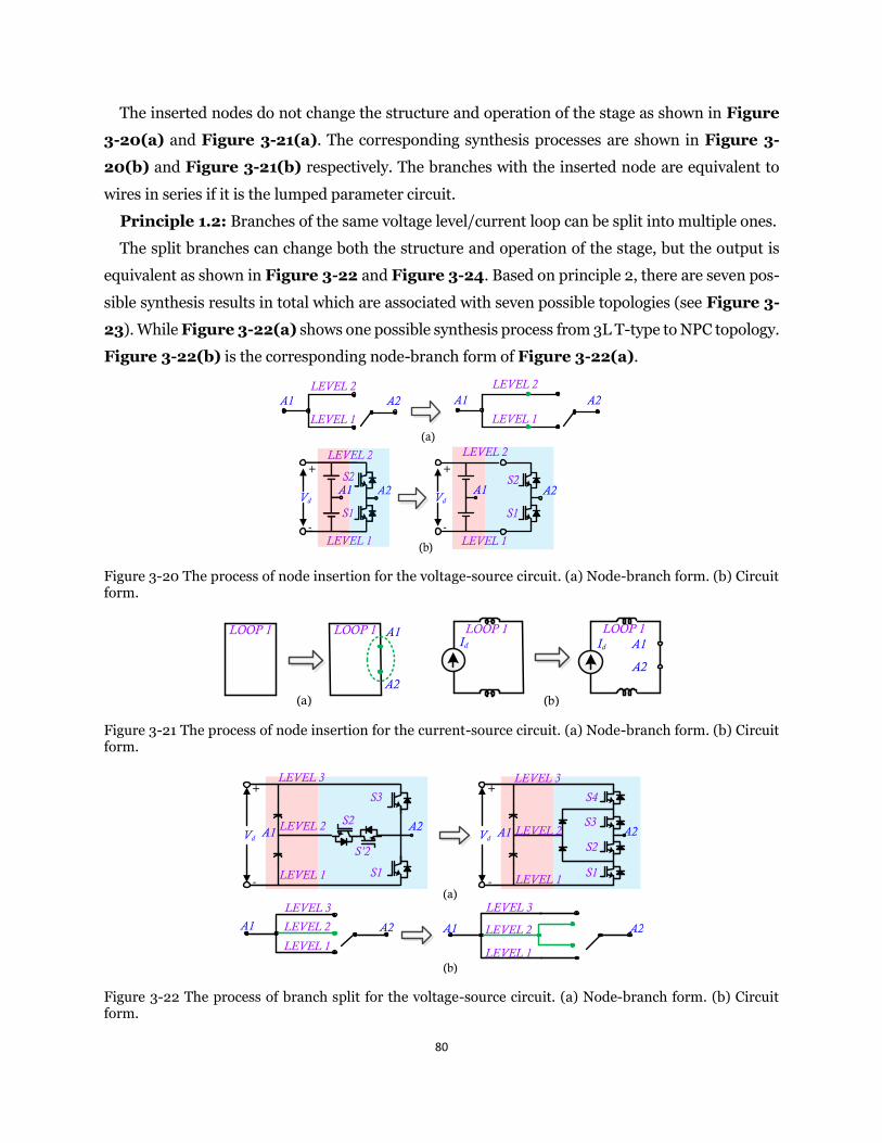
80
The inserted nodes do not change the structure and operation of the stage as shown in Figure
3-20(a) and Figure 3-21(a). The corresponding synthesis processes are shown in Figure 3-
20(b) and Figure 3-21(b) respectively. The branches with the inserted node are equivalent to
wires in series if it is the lumped parameter circuit.
Principle 1.2: Branches of the same voltage level/current loop can be split into multiple ones.
The split branches can change both the structure and operation of the stage, but the output is
equivalent as shown in Figure 3-22 and Figure 3-24. Based on principle 2, there are seven pos-
sible synthesis results in total which are associated with seven possible topologies (see Figure 3-
23). While Figure 3-22(a) shows one possible synthesis process from 3L T-type to NPC topology.
Figure 3-22(b) is the corresponding node-branch form of Figure 3-22(a).
LEVEL 2
LEVEL 1
A1 A2LEVEL 2
LEVEL 1
A1 A2
Vd
+
-
A2S2
S1
LEVEL 2
LEVEL 1
A1S2
S1
LEVEL 2
LEVEL 1
A1 A2S2
S1
LEVEL 2
LEVEL 1
A1Vd
+
-
A2S2
S1
LEVEL 2
LEVEL 1
A1
(a)
(b) Figure 3-20 The process of node insertion for the voltage-source circuit. (a) Node-branch form. (b) Circuit form.
LOOP 1 A1
A2
LOOP 1 LOOP 1A1
A2
Id
LOOP 1
(a) (b)
Id
Figure 3-21 The process of node insertion for the current-source circuit. (a) Node-branch form. (b) Circuit form.
LEVEL 3
LEVEL 2
LEVEL 1
LEVEL 3
LEVEL 2
LEVEL 1
A1 A2 A1 A2
Vd
+
-
A2
S4
S3
S2
S1
A1
LEVEL 3
LEVEL 2
LEVEL 1
Vd
+
-
A2
S3
S1
S2
S
A1
LEVEL 3
LEVEL 2
LEVEL 1
(a)
(b) Figure 3-22 The process of branch split for the voltage-source circuit. (a) Node-branch form. (b) Circuit form.
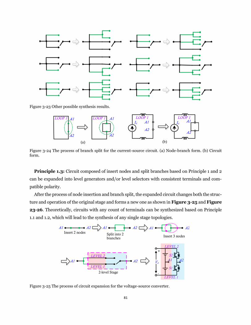
81
Figure 3-23 Other possible synthesis results.
A1
A2
A1
A2
LOOP 1 LOOP 1 LOOP 1A1
A2
Id
LOOP 1A1
A2
Id
(b)(a) Figure 3-24 The process of branch split for the current-source circuit. (a) Node-branch form. (b) Circuit form.
Principle 1.3: Circuit composed of insert nodes and split branches based on Principle 1 and 2
can be expanded into level generators and/or level selectors with consistent terminals and com-
patible polarity.
After the process of node insertion and branch split, the expanded circuit changes both the struc-
ture and operation of the original stage and forms a new one as shown in Figure 3-25 and Figure
23-26. Theoretically, circuits with any count of terminals can be synthesized based on Principle
1.1 and 1.2, which will lead to the synthesis of any single stage topologies.
A1 A2 A1 A2 A1 A2
A1 A2LEVEL 2
LEVEL 1
2-level Stage
Insert 2 nodes Split into 2 branches Insert 3 nodes
Vd
+
-
A2S2
S1
LEVEL 2
LEVEL 1
A1S2
S1
LEVEL 2
LEVEL 1
A1 A2S2
S1
LEVEL 2
LEVEL 1
A1A1
Figure 3-25 The process of circuit expansion for the voltage-source converter.
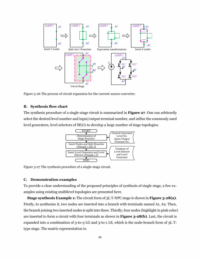
82
A1
A2
LOOP 1
B2
B1
LOOP 1 A1
A2
Insert 2 nodes Split into 3 branches
3-level Stage
LOOP 1 A1
A2
LOOP 1 A1
A2
Insert 6 nodesEquivalent transformation
LOOP 1 A1
A2
B2B1
LOOP 1A1
A2
S11'S11
S12'S12
Id
Figure 3-26 The process of circuit expansion for the current-source converter.
B. Synthesis flow chart
The synthesis procedure of a single-stage circuit is summarized in Figure 27. One can arbitrarily
select the desired level number and input/output terminal number, and utilize the commonly used
level generators, level selectors of MLCs to develop a large number of stage topologies.
Determination of Stage Structure
START
Insert Nodes and Split Branches (Principle 1.1&1.2)
Insert Level Generator and Level Selector (Principle 1.3)
END
Desired Generated Level No.
Input/Output Terminal No.
Database of Level Selector
and Level Generator
Figure 3-27 The synthesis procedure of a single-stage circuit.
C. Demonstration examples
To provide a clear understanding of the proposed principles of synthesis of single stage, a few ex-
amples using existing multilevel topologies are presented here.
Stage synthesis Example 1: The circuit form of 3L T-NPC stage is shown in Figure 3-28(a).
Firstly, to synthesize it, two nodes are inserted into a branch with terminals named A1, A2. Then,
the branch joining two inserted nodes is split into three. Thirdly, four nodes (highlight in pink color)
are inserted to form a circuit with four terminals as shown in Figure 3-28(b). Last, the circuit is
expanded into a combination of 3-to-3 LG and 3-to-1 LS, which is the node-branch form of 3L T-
type stage. The matrix representation is:
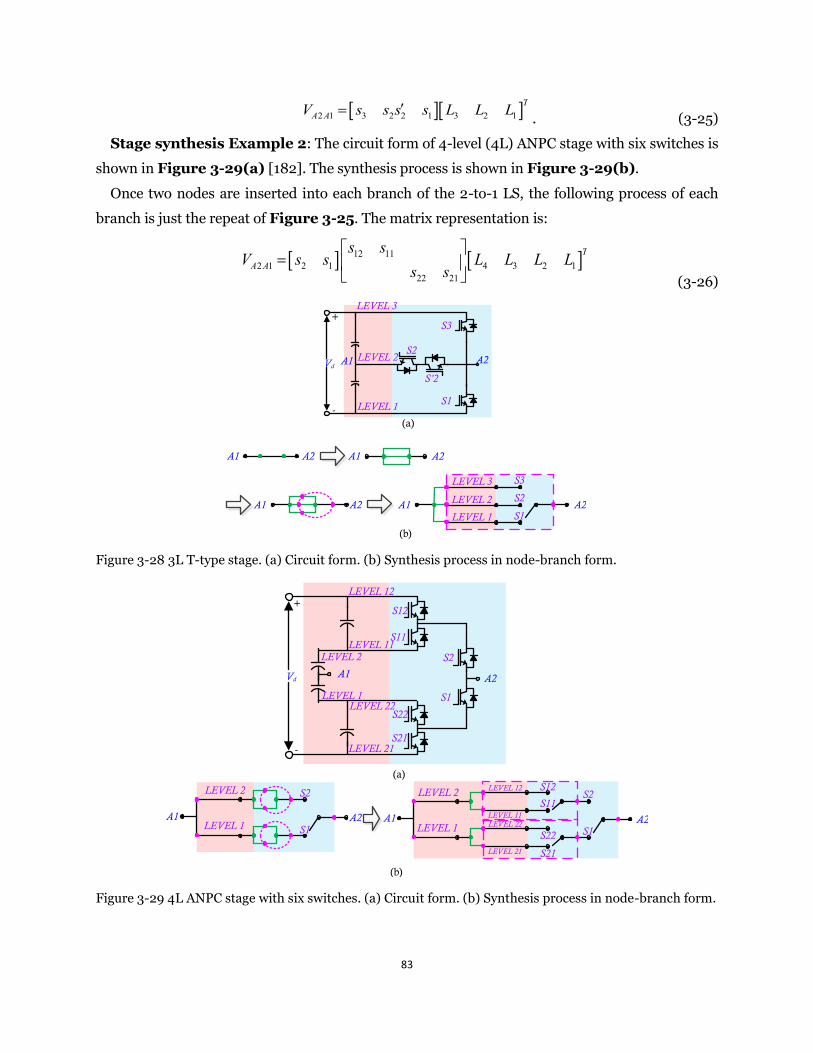
83
2 1 3 2 2 1 3 2 1T
A AV s s s s L L L=. (3-25)
Stage synthesis Example 2: The circuit form of 4-level (4L) ANPC stage with six switches is
shown in Figure 3-29(a) [182]. The synthesis process is shown in Figure 3-29(b).
Once two nodes are inserted into each branch of the 2-to-1 LS, the following process of each
branch is just the repeat of Figure 3-25. The matrix representation is:
12 112 1 2 1 4 3 2 1
22 21
TA A
s sV s s L L L L
s s
= (3-26)
Vd
+
-
A2
S3
S1
S2
S
A1
LEVEL 3
LEVEL 2
LEVEL 1
A1 A2 A1 A2
A1 A2 A1 A2
LEVEL 3
LEVEL 2
LEVEL 1
S3
S2
S1
(b)
(a)
Figure 3-28 3L T-type stage. (a) Circuit form. (b) Synthesis process in node-branch form.
Vd
+
-
A2
S12
S11
S22
S21
S1
A1
LEVEL 12
LEVEL 11S2
LEVEL 22
LEVEL 21
LEVEL 2
LEVEL 1
A1 A2 A1 A2
LEVEL 12
LEVEL 11LEVEL 22
LEVEL 21
S12
S11
S22
S21
LEVEL 1
LEVEL 2 S2
S1
S2
S1LEVEL 1
LEVEL 2
(b)
(a)
Figure 3-29 4L ANPC stage with six switches. (a) Circuit form. (b) Synthesis process in node-branch form.
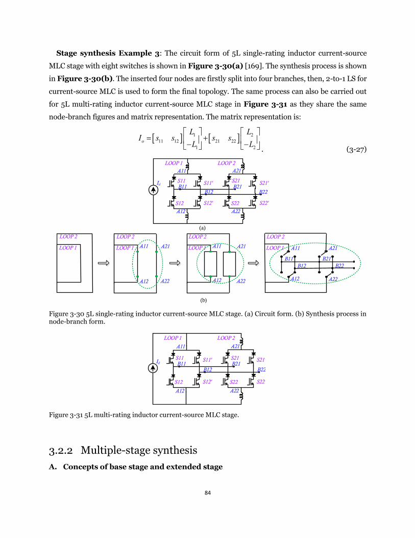
84
Stage synthesis Example 3: The circuit form of 5L single-rating inductor current-source
MLC stage with eight switches is shown in Figure 3-30(a) [169]. The synthesis process is shown
in Figure 3-30(b). The inserted four nodes are firstly split into four branches, then, 2-to-1 LS for
current-source MLC is used to form the final topology. The same process can also be carried out
for 5L multi-rating inductor current-source MLC stage in Figure 3-31 as they share the same
node-branch figures and matrix representation. The matrix representation is:
1 211 12 21 22
1 2o
L LI s s s s
L L
= + − − . (3-27)
LOOP 1
LOOP 2
LOOP 1
LOOP 2
A11
A12
A21
A22
LOOP 1
LOOP 2
A11
A12
A21
A22
LOOP 1
LOOP 2
A11
A12
A21
A22
B12B11
B22B21
B12B11
LOOP 1A11
A12
Id
B22B21
A21
A22
LOOP 2
S11'S11
S12'S12
S21'S21
S22'S22
(a)
(b) Figure 3-30 5L single-rating inductor current-source MLC stage. (a) Circuit form. (b) Synthesis process in node-branch form.
B12B11
LOOP 1
A11
A12
B22B21
A21
A22
LOOP 2
S11'S11
S12'S12
S21'S21
S22'S22
Id
Figure 3-31 5L multi-rating inductor current-source MLC stage.
3.2.2 Multiple-stage synthesis
A. Concepts of base stage and extended stage
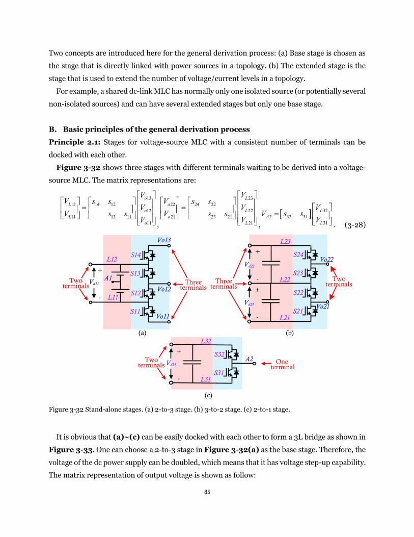
85
Two concepts are introduced here for the general derivation process: (a) Base stage is chosen as
the stage that is directly linked with power sources in a topology. (b) The extended stage is the
stage that is used to extend the number of voltage/current levels in a topology.
For example, a shared dc-link MLC has normally only one isolated source (or potentially several
non-isolated sources) and can have several extended stages but only one base stage.
B. Basic principles of the general derivation process
Principle 2.1: Stages for voltage-source MLC with a consistent number of terminals can be
docked with each other.
Figure 3-32 shows three stages with different terminals waiting to be derived into a voltage-
source MLC. The matrix representations are:
1314 1212
1213 1111
11
oL
oL
o
Vs sV
Vs sV
V
= ,
2322 24 22
2221 23 21
21
Lo
Lo
L
VV s s
VV s s
V
= ,
322 32 31
31
LA
L
VV s s
V
= . (3-28)
S14
S13
S12
S11
L12
L11
+
-
Vd11A1
Vo12
Vo13
Vo11
+
-
L23
L22
+
- L21
S24
S23
S22
S21Vo21
Vo22Vd22
Vd21
L32
+
- L31
S32
S31
Vd31A2
Three terminals
Two terminals
Two terminalsThree
terminals
Two terminals One
terminal
(a) (b)
(c) Figure 3-32 Stand-alone stages. (a) 2-to-3 stage. (b) 3-to-2 stage. (c) 2-to-1 stage.
It is obvious that (a)~(c) can be easily docked with each other to form a 3L bridge as shown in
Figure 3-33. One can choose a 2-to-3 stage in Figure 3-32(a) as the base stage. Therefore, the
voltage of the dc power supply can be doubled, which means that it has voltage step-up capability.
The matrix representation of output voltage is shown as follow:
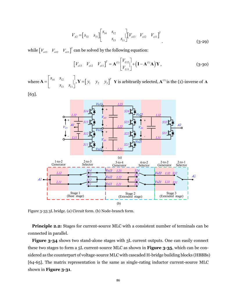
86
14 122 32 31 13 12 11
13 11
TA o o o
s sV s s V V V
s s
= . (3-29)
while 13 12 11T
o o oV V V can be solved by the following equation:
( )12(1) (1)13 12 11
11
T Lo o o
L
VV V V
V
= + −
A I A A Y , (3-30)
where 14 121 2 3
13 11
, Ts sy y y
s s
= =
A Y Y is arbitrarily selected, (1)A is the {1}-inverse of A
[63].
Vd22
+
-
L23
L22
Vd21
+
- L21
S24
S23
S22
S21Vo21
Vo22 L32
+
- L31
S32
S31
Vd31
S14
S13
S12
S11
L12
L11
+
-
Vd11A1 A2
Vo12
Vo13
Vo11
A1L11
L12
S12S11 L21
L23
L22 A2
S14S13
Vo12
Vo13
Vo11S22S21
S24S23 Vo22
Vo21 L31
L32 S32
S31
1-to-2 Generator
2-to-3 Selector
3-to-4 Generator
4-to-2 Selector
2-to-2 Generator
2-to-1 Selector
Stage 1 (Base stage)
Stage 2(Extended stage)
Stage 3(Extended stage)
(a)
(b) Figure 3-33 3L bridge. (a) Circuit form. (b) Node-branch form.
Principle 2.2: Stages for current-source MLC with a consistent number of terminals can be
connected in parallel.
Figure 3-34 shows two stand-alone stages with 3L current outputs. One can easily connect
these two stages to form a 5L current-source MLC as shown in Figure 3-35, which can be con-
sidered as the counterpart of voltage-source MLC with cascaded H-bridge building blocks (HBBBs)
[64-65]. The matrix representation is the same as single-rating inductor current-source MLC
shown in Figure 3-31.
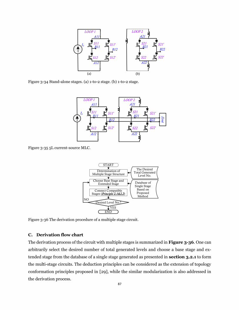
87
B22B21
A21
A22
LOOP 2
S21'S21
S22'S22
B12B11
LOOP 1
A11
A12
S11'S11
S12'S12
Id
(a) (b)
Figure 3-34 Stand-alone stages. (a) 1-to-2 stage. (b) 1-to-2 stage.
B12B11
LOOP 1
A11
A12
B22B21
A21
A22
LOOP 2
S11'S11
S12'S12
S21'S21
S22'S22
Zou
t
Id
Figure 3-35 5L current-source MLC.
Determination of Multiple Stage Structure
START
Choose Base Stage and Extended Stage
Connect Compatible Stages (Principle 2.1&2.2)
END
The Desired Total Generated
Level No.
Database of Single Stage
Based on Proposed Method
Desired Level No.?
YES
NO
Figure 3-36 The derivation procedure of a multiple stage circuit.
C. Derivation flow chart
The derivation process of the circuit with multiple stages is summarized in Figure 3-36. One can
arbitrarily select the desired number of total generated levels and choose a base stage and ex-
tended stage from the database of a single stage generated as presented in section 3.2.1 to form
the multi-stage circuits. The deduction principles can be considered as the extension of topology
conformation principles proposed in [29], while the similar modularization is also addressed in
the derivation process.
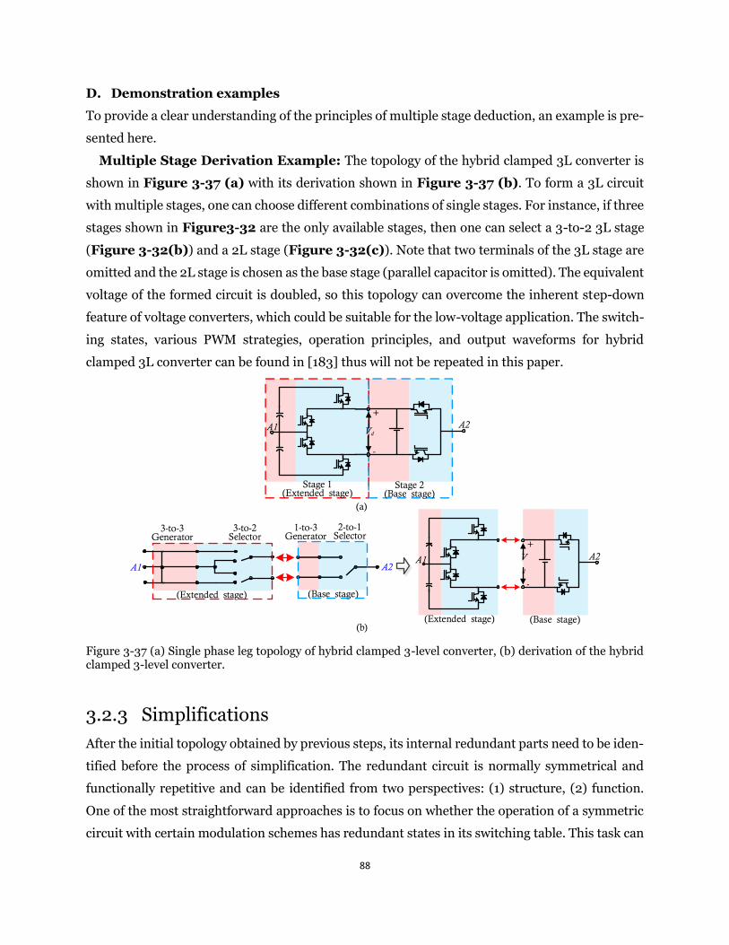
88
D. Demonstration examples
To provide a clear understanding of the principles of multiple stage deduction, an example is pre-
sented here.
Multiple Stage Derivation Example: The topology of the hybrid clamped 3L converter is
shown in Figure 3-37 (a) with its derivation shown in Figure 3-37 (b). To form a 3L circuit
with multiple stages, one can choose different combinations of single stages. For instance, if three
stages shown in Figure3-32 are the only available stages, then one can select a 3-to-2 3L stage
(Figure 3-32(b)) and a 2L stage (Figure 3-32(c)). Note that two terminals of the 3L stage are
omitted and the 2L stage is chosen as the base stage (parallel capacitor is omitted). The equivalent
voltage of the formed circuit is doubled, so this topology can overcome the inherent step-down
feature of voltage converters, which could be suitable for the low-voltage application. The switch-
ing states, various PWM strategies, operation principles, and output waveforms for hybrid
clamped 3L converter can be found in [183] thus will not be repeated in this paper.
Stage 1(Extended stage)
Stage 2(Base stage)
Stage 2Stage 2Stage 2
Vd
+
-
A2A1
A1 A2
(Base stage)(Extended stage)
3-to-3 Generator
1-to-3 Generator
3-to-2 Selector
2-to-1 Selector
Vd
+
-
A2A1
(Extended stage) (Base stage)
(a)
(b) Figure 3-37 (a) Single phase leg topology of hybrid clamped 3-level converter, (b) derivation of the hybrid clamped 3-level converter.
3.2.3 Simplifications
After the initial topology obtained by previous steps, its internal redundant parts need to be iden-
tified before the process of simplification. The redundant circuit is normally symmetrical and
functionally repetitive and can be identified from two perspectives: (1) structure, (2) function.
One of the most straightforward approaches is to focus on whether the operation of a symmetric
circuit with certain modulation schemes has redundant states in its switching table. This task can
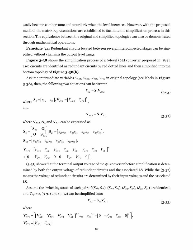
89
easily become cumbersome and unorderly when the level increases. However, with the proposed
method, the matrix representations are established to facilitate the simplification process in this
section. The equivalence between the original and simplified topologies can also be demonstrated
through mathematical operations.
Principle 3.1: Redundant circuits located between several interconnected stages can be sim-
plified without changing the output level range.
Figure 3-38 shows the simplification process of a 9-level (9L) converter proposed in [184].
Two circuits are identified as redundant circuits by red dotted lines and then simplified into the
bottom topology of Figure 3-38(b).
Assume intermediate variables VoX1, VoX2, VoY1, VoY2 in original topology (see labels in Figure
3-38), then, the following two equations can be written:
2 3 2A XYV = S V (3-31)
where 3 36 35 2 2 2, T
XY oX oYs s V V= =S V,
and
2 2 1XY XY=V S V (3-32)
where VXY2, S2, and VXY1 can be expressed as:
212 21 28 34 28 33 27 34 27 33
22
22 26 32 26 31 25 32 25 31
, ,
,
s s s s s s s s
s s s s s s s s
= =
=
S OS S
O S
S
32 32 31 31
1 1 1 1 1 1 1 1 1
0 0 0 0 .
TXY oX oX oX oX oY oY oY
d
oY
d dT
d
V V V V V V
V
V V
V V V
=
+ −−
V
(3-31) shows that the terminal output voltage of the 9L converter before simplification is deter-
mined by both the output voltage of redundant circuits and the associated LS. While the (3-32)
means the voltage of redundant circuits are determined by their input voltages and the associated
LS.
Assume the switching states of each pair of (S28, S26), (S27, S25), (S34, S32), (S33, S31) are identical,
and Vd32=0, (3-31) and (3-32) can be simplified into:
2 22 1A XYV = S V (3-33)
where
1 31 1 1 1 36 35
1
1 31
1 1
0 0 ,
.
T T TXY XY XY XY XY
XY o
d
X oY
ds Vs
V
V
V
= +
−
=
V V V V V
V
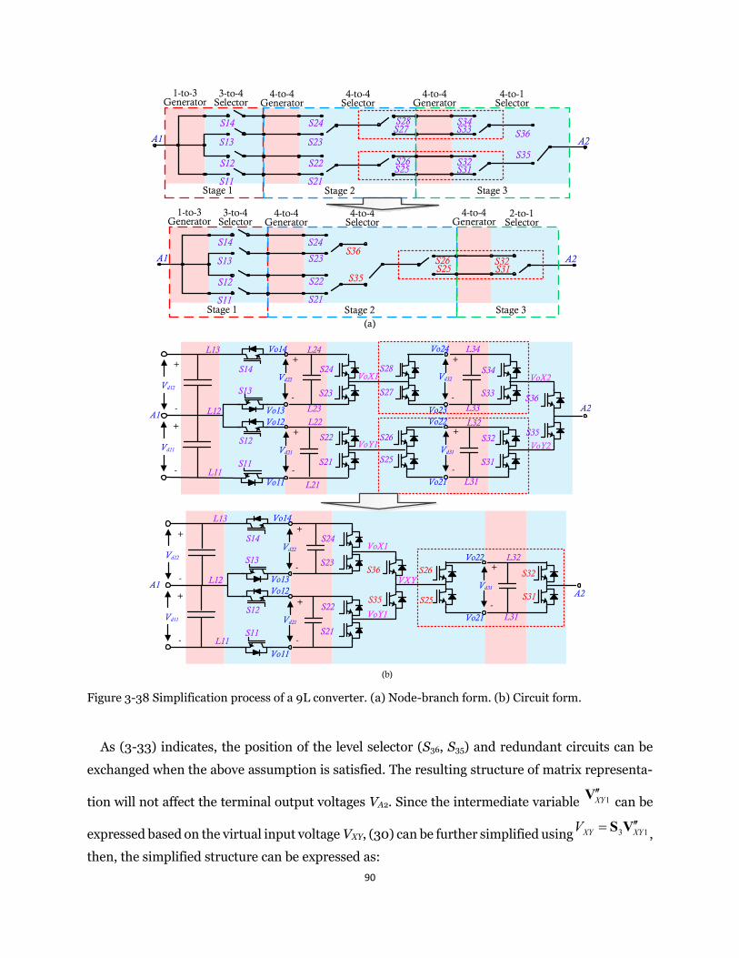
90
1-to-3 Generator
A1
3-to-4 Selector
4-to-4 Generator
4-to-4Selector
4-to-4 Generator
4-to-1Selector
A2
Stage 1 Stage 2 Stage 3
1-to-3 Generator
A1
3-to-4 Selector
4-to-4 Generator
4-to-4Selector
4-to-4 Generator
2-to-1Selector
Stage 1 Stage 2 Stage 3
A2
S14
S13
S12
S11
S24
S23
S22
S21
S28S27
S26S25
S34S33
S32S31
S36
S35
S14
S13
S12
S11
S24
S23
S22
S21
S26S25
S36
S35
S32S31
(a)
4 to 4
Vd12
+
-
Vd11
+
-
+
-
Vd22
+
-
Vd21
+
-
Vd32
+
-
Vd31
A2A1
Vd12
+
-
Vd11
+
-
+
-
Vd22
+
-
Vd21
A2A1
+
-
Vd31
S14
S13
S12
S11
S24
S23
S22
S21
S28
S27
S26
S25
S34
S33
S32
S31
S36
S35
S14
S13
S12
S11
S24
S23
S22
S21
S36
S35
S32
S31
L12
L11
Vo12Vo13
Vo11
Vo14L13
L22
L21
L24
L23Vo22Vo23
Vo21
Vo24
L32
L31
L34
L33
L12
L11
Vo12Vo13
Vo11
Vo14L13
Vo22
Vo21
L32
L31
S26
S25
VoY1
VoX1
VoY2
VoX2
VXY
VoY1
VoX1
(b) Figure 3-38 Simplification process of a 9L converter. (a) Node-branch form. (b) Circuit form.
As (3-33) indicates, the position of the level selector (S36, S35) and redundant circuits can be
exchanged when the above assumption is satisfied. The resulting structure of matrix representa-
tion will not affect the terminal output voltages VA2. Since the intermediate variable 1XYV can be
expressed based on the virtual input voltage VXY, (30) can be further simplified using 3 1XXY YV = S V,
then, the simplified structure can be expressed as:
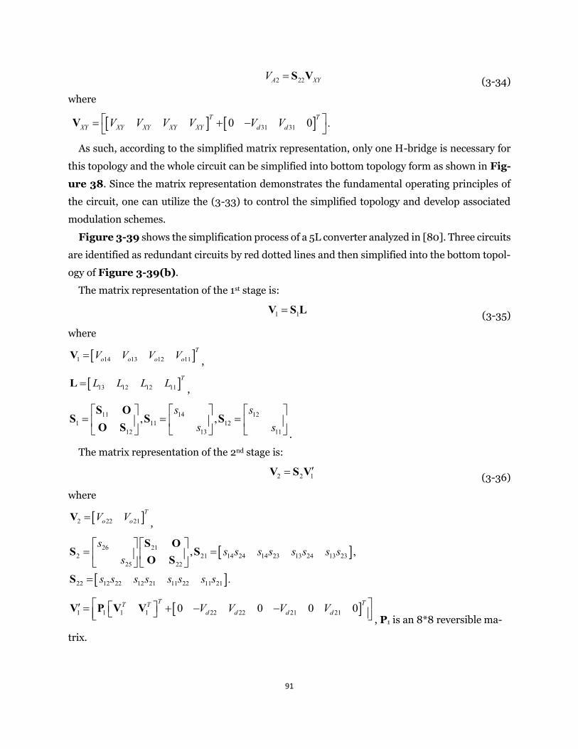
91
2 22A XYV = S V (3-34)
where
31 310 0 .XY XY XY XY XY d
T TdV V V V V V = +
−
V
As such, according to the simplified matrix representation, only one H-bridge is necessary for
this topology and the whole circuit can be simplified into bottom topology form as shown in Fig-
ure 38. Since the matrix representation demonstrates the fundamental operating principles of
the circuit, one can utilize the (3-33) to control the simplified topology and develop associated
modulation schemes.
Figure 3-39 shows the simplification process of a 5L converter analyzed in [80]. Three circuits
are identified as redundant circuits by red dotted lines and then simplified into the bottom topol-
ogy of Figure 3-39(b).
The matrix representation of the 1st stage is:
1 1=V S L (3-35)
where
1 14 13 12 11T
o o o oV V V V=V,
13 12 12 11TL L L L=L
,
1411 121 11 12
1312 11
, ,s s
s s
= = =
S OS S S
O S.
The matrix representation of the 2nd stage is:
2 2 1=V S V (3-36)
where
2 22 21T
o oV V=V,
26 212 21 14 24 14 23 13 24 13 23
25 22
22 12 22 12 21 11 22 11 21
, ,
.
ss s s s s s s s
s
s s s s s s s s
= =
=
S OS S
O S
S
1 1 1 1 22 22 21 210 0 0 0T TT T
d d d dV V V V = + − − V P V V
, P1 is an 8*8 reversible ma-
trix.
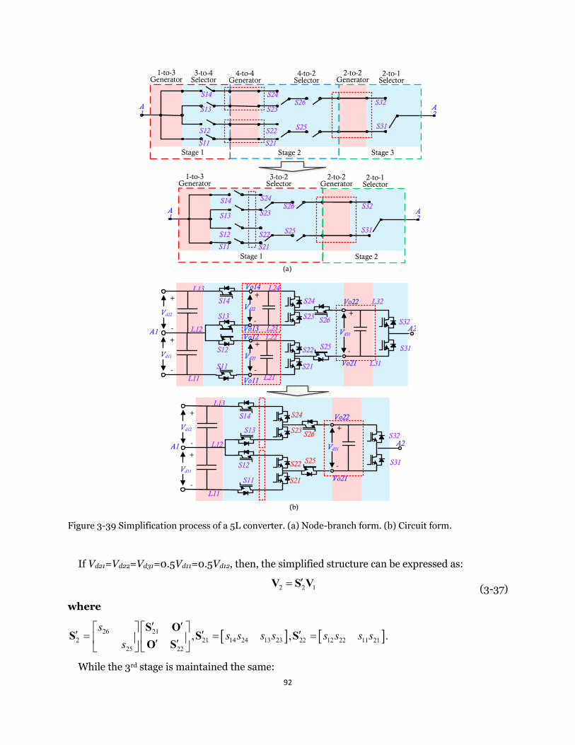
92
1-to-3 Generator
A1
3-to-4 Selector
4-to-4 Generator
4-to-2Selector
2-to-2Generator
2-to-1Selector
Stage 1 Stage 2 Stage 3
A2
1-to-3 Generator
A1
3-to-2 Selector
Stage 1
2-to-2 Generator
2-to-1Selector
Stage 2
A2
S14
S13
S12
S11
S24
S23
S22
S21
S26
S25
S32
S31
S14
S13
S12
S11
S24
S23
S22
S21
S26
S25
S32
S31
(a)
Vd12
+
-
Vd11
+
-
+
-
Vd22
+
-
Vd21
A2A1
+
-
Vd31
Vd12
+
-
Vd11
+
-
A2A1
+
-
Vd31
S14
S13
S12
S11
Vo12Vo13
Vo11
Vo14 L24
L23L22
L21
L13
L12
L11
S24
S23
S22
S21
S26
S25
S32
S31
S24
S23
S22
S21
S26
S25
S32
S31
S14
S13
S12
S11
L13
L12
L11
Vo21
Vo22 L32
L31
Vo21
Vo22
(b) Figure 3-39 Simplification process of a 5L converter. (a) Node-branch form. (b) Circuit form.
If Vd21=Vd22=Vd31=0.5Vd11=0.5Vd12, then, the simplified structure can be expressed as:
2 2 1=V S V (3-37)
where
26 212 21 14 24 13 23 22 12 22 11 21
25 22
, , .s
s s s s s s s ss
= = =
S OS S S
O S
While the 3rd stage is maintained the same:
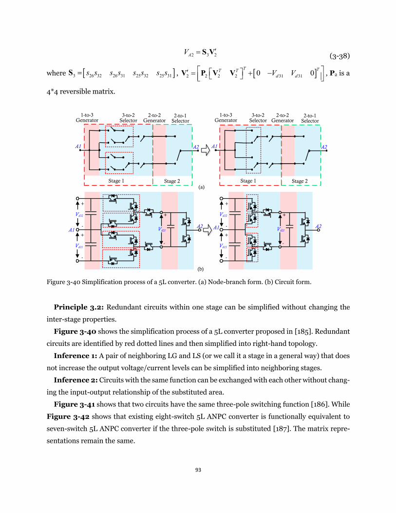
93
2 3 2AV = S V (3-38)
where 3 26 32 26 31 25 32 25 31s s s s s s s s=S , 2 2 2 2 31 310 0T TT T
d dV V = + − V P V V , P2 is a
4*4 reversible matrix.
1-to-3 Generator
A1
3-to-2 Selector
Stage 1
2-to-2Generator
2-to-1Selector
Stage 2
A2
1-to-3 Generator
A1
3-to-2 Selector
Stage 1
2-to-2Generator
2-to-1Selector
Stage 2
A2
Vd12
+
-
Vd11
+
-
A2A1
+
-
Vd21
Vd12
+
-
Vd11
+
-
A2A1
+
-
Vd21
(a)
(b) Figure 3-40 Simplification process of a 5L converter. (a) Node-branch form. (b) Circuit form.
Principle 3.2: Redundant circuits within one stage can be simplified without changing the
inter-stage properties.
Figure 3-40 shows the simplification process of a 5L converter proposed in [185]. Redundant
circuits are identified by red dotted lines and then simplified into right-hand topology.
Inference 1: A pair of neighboring LG and LS (or we call it a stage in a general way) that does
not increase the output voltage/current levels can be simplified into neighboring stages.
Inference 2: Circuits with the same function can be exchanged with each other without chang-
ing the input-output relationship of the substituted area.
Figure 3-41 shows that two circuits have the same three-pole switching function [186]. While
Figure 3-42 shows that existing eight-switch 5L ANPC converter is functionally equivalent to
seven-switch 5L ANPC converter if the three-pole switch is substituted [187]. The matrix repre-
sentations remain the same.
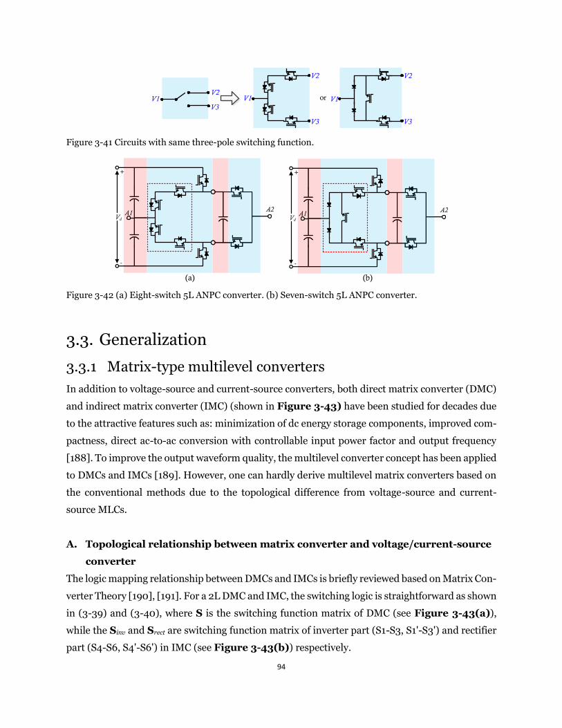
94
orV1V2
V3V1
V2
V3
V1
V2
V3 Figure 3-41 Circuits with same three-pole switching function.
A2Vd
+
-
+
A1 A2Vd
+
-
+
A1
(a) (b) Figure 3-42 (a) Eight-switch 5L ANPC converter. (b) Seven-switch 5L ANPC converter.
3.3. Generalization
3.3.1 Matrix-type multilevel converters
In addition to voltage-source and current-source converters, both direct matrix converter (DMC)
and indirect matrix converter (IMC) (shown in Figure 3-43) have been studied for decades due
to the attractive features such as: minimization of dc energy storage components, improved com-
pactness, direct ac-to-ac conversion with controllable input power factor and output frequency
[188]. To improve the output waveform quality, the multilevel converter concept has been applied
to DMCs and IMCs [189]. However, one can hardly derive multilevel matrix converters based on
the conventional methods due to the topological difference from voltage-source and current-
source MLCs.
A. Topological relationship between matrix converter and voltage/current-source
converter
The logic mapping relationship between DMCs and IMCs is briefly reviewed based on Matrix Con-
verter Theory [190], [191]. For a 2L DMC and IMC, the switching logic is straightforward as shown
in (3-39) and (3-40), where S is the switching function matrix of DMC (see Figure 3-43(a)),
while the Sinv and Srect are switching function matrix of inverter part (S1-S3, S1'-S3') and rectifier
part (S4-S6, S4'-S6') in IMC (see Figure 3-43(b)) respectively.
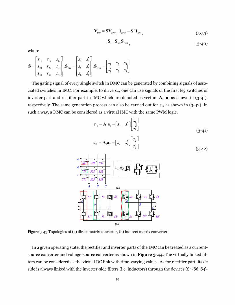
95
inv rect=V SV,
Trect inv=I S I
, (3-39)
inv rect=S S S, (3-40)
where
11 12 13 4 41 2 3
21 22 23 5 51 2 3
31 32 33 6 6
, ,inv rect
s s s s ss s s
s s s s ss s s
s s s s s
= = =
S S S
,
The gating signal of every single switch in DMC can be generated by combining signals of asso-
ciated switches in IMC. For example, to drive s11, one can use signals of the first leg switches of
inverter part and rectifier part in IMC which are denoted as vectors A1, a1 as shown in (3-41),
respectively. The same generation process can also be carried out for s12 as shown in (3-42). In
such a way, a DMC can be considered as a virtual IMC with the same PWM logic.
111 1 1 4 4
1
ss s s
s
= = A a
(3-41)
212 1 2 4 4
2
ss s s
s
= = A a
(3-42)
b
a
c
BA C
S11 S21 S31
S12 S22 S32
S13 S23 S33
ba
S1'
S1
S2'
S2
c
S3
S3'
BA
S4'
S4
S5'
S5
C
S6
S6'
(a)
(b) Figure 3-43 Topologies of (a) direct matrix converter, (b) indirect matrix converter.
In a given operating state, the rectifier and inverter parts of the IMC can be treated as a current-
source converter and voltage-source converter as shown in Figure 3-44. The virtually linked fil-
ters can be considered as the virtual DC link with time-varying values. As for rectifier part, its dc
side is always linked with the inverter-side filters (i.e. inductors) through the devices (S4-S6, S4'-
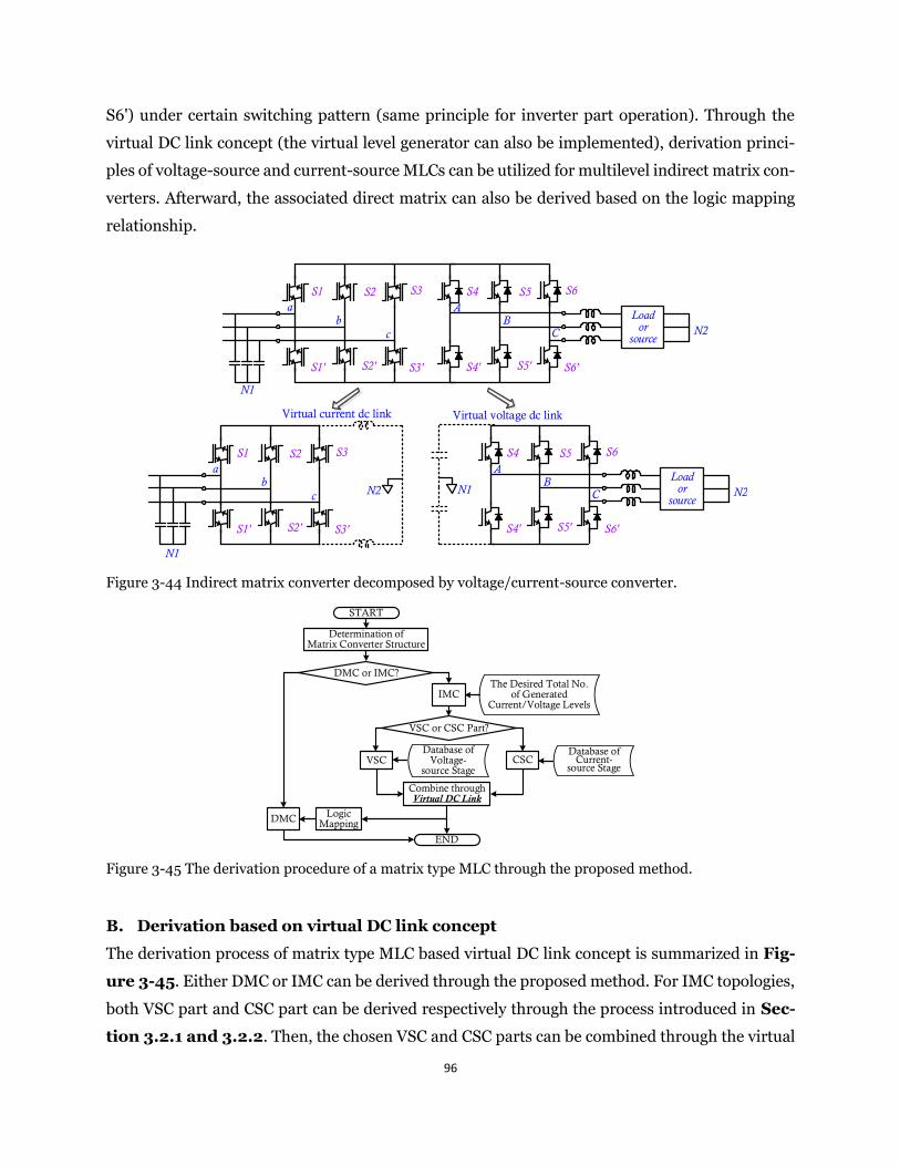
96
S6') under certain switching pattern (same principle for inverter part operation). Through the
virtual DC link concept (the virtual level generator can also be implemented), derivation princi-
ples of voltage-source and current-source MLCs can be utilized for multilevel indirect matrix con-
verters. Afterward, the associated direct matrix can also be derived based on the logic mapping
relationship.
ba
S1'
S1
S2'
S2
c
S3
S3'
BA
S4'
S4
S5'
S5
C
S6
S6'
ba
S1'
S1
S2'
S2
c
S3
S3'
BA
S4'
S4
S5'
S5
C
S6
S6'
N1
N2Load
or source
N2 N1
N1
N2Load
or source
Virtual current dc link Virtual voltage dc link
Figure 3-44 Indirect matrix converter decomposed by voltage/current-source converter.
The Desired Total No. of Generated
Current/Voltage Levels
Database of Current-
source Stage
Determination of Matrix Converter Structure
START
DMC or IMC?
DMC
IMC
Logic Mapping
END
Combine through Virtual DC Link
VSC or CSC Part?
VSC CSCDatabase of
Voltage-source Stage
Figure 3-45 The derivation procedure of a matrix type MLC through the proposed method.
B. Derivation based on virtual DC link concept
The derivation process of matrix type MLC based virtual DC link concept is summarized in Fig-
ure 3-45. Either DMC or IMC can be derived through the proposed method. For IMC topologies,
both VSC part and CSC part can be derived respectively through the process introduced in Sec-
tion 3.2.1 and 3.2.2. Then, the chosen VSC and CSC parts can be combined through the virtual
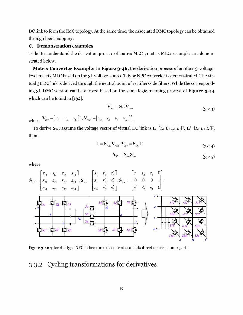
97
DC link to form the IMC topology. At the same time, the associated DMC topology can be obtained
through logic mapping.
C. Demonstration examples
To better understand the derivation process of matrix MLCs, matrix MLCs examples are demon-
strated below.
Matrix Converter Example: In Figure 3-46, the derivation process of another 3-voltage-
level matrix MLC based on the 3L voltage-source T-type NPC converter is demonstrated. The vir-
tual 3L DC link is derived through the neutral point of rectifier-side filters. While the correspond-
ing 3L DMC version can be derived based on the same logic mapping process of Figure 3-44
which can be found in [192].
3inv L rect=V S V (3-43)
where 1,T T
inv A B C rect a b c Nv v v v v v v= =V V.
To derive S3L, assume the voltage vector of virtual DC link is L=[L3 L2 L2 L1]T, L'=[L3 L2 L1]T,
then,
,rect rect inv inv = =L S V V S L (3-44)
3L inv rect=S S S (3-45)
where
11 12 13 14 4 4 4 1 2 3
3 21 22 23 24 5 5 5
31 32 33 34 6 6 6 1 2 3
0, , 0 0 0 1
0L inv rect
s s s s s s s s s ss s s s s s ss s s s s s s s s s
= = =
S S S .
b
a
c
B
A
CN1
b
a
c
A B C
N1S1'
S1
S2'
S2 S3
S3'
S4'S4
S5'
S5 S6
S6'
S4'' S5'' S6''
S11 S21 S31
S12 S22 S32
S13 S23 S33
S14 S24 S34
Figure 3-46 3-level T-type NPC indirect matrix converter and its direct matrix counterpart.
3.3.2 Cycling transformations for derivatives
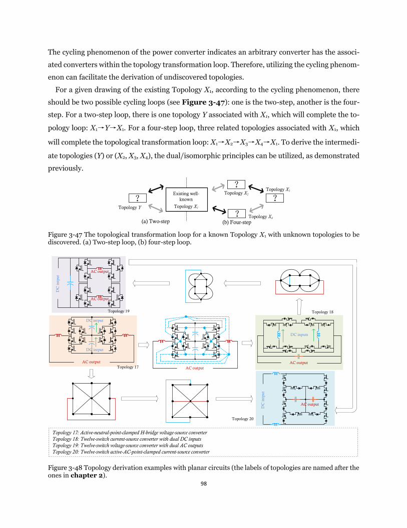
98
The cycling phenomenon of the power converter indicates an arbitrary converter has the associ-
ated converters within the topology transformation loop. Therefore, utilizing the cycling phenom-
enon can facilitate the derivation of undiscovered topologies.
For a given drawing of the existing Topology X1, according to the cycling phenomenon, there
should be two possible cycling loops (see Figure 3-47): one is the two-step, another is the four-
step. For a two-step loop, there is one topology Y associated with X1, which will complete the to-
pology loop: X1→Y→X1. For a four-step loop, three related topologies associated with X1, which
will complete the topological transformation loop: X1→X2→X3→X4→X1. To derive the intermedi-
ate topologies (Y) or (X2, X3, X4), the dual/isomorphic principles can be utilized, as demonstrated
previously.
?
?
Topology X2
Topology X4
?Topology X3
(a) Two-step
Existing well-known
Topology X1
(b) Four-step
?Topology Y
Figure 3-47 The topological transformation loop for a known Topology X1 with unknown topologies to be discovered. (a) Two-step loop, (b) four-step loop.
AC outputTopology 17
Topology 18Topology 19
Topology 20
AC outputAC output
DC
intp
ut
DC
intp
ut
Topology 17: Active-neutral-point-clamped H-bridge voltage-source converterTopology 18: Twelve-switch current-source converter with dual DC inputsTopology 19: Twelve-switch voltage-source converter with dual AC outputsTopology 20: Twelve-switch active-AC-point-clamped current-source converter
DC inputs
AC output
AC output
AC output
DC intput
DC intput
Figure 3-48 Topology derivation examples with planar circuits (the labels of topologies are named after the ones in chapter 2).
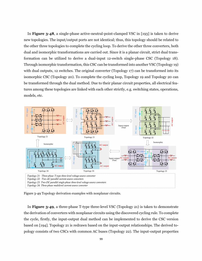
99
In Figure 3-48, a single-phase active-neutral-point-clamped VSC in [193] is taken to derive
new topologies. The input/output ports are not identical; thus, this topology should be related to
the other three topologies to complete the cycling loop. To derive the other three converters, both
dual and isomorphic transformations are carried out. Since it is a planar circuit, strict dual trans-
formation can be utilized to derive a dual-input 12-switch single-phase CSC (Topology 18).
Through isomorphic transformation, this CSC can be transformed into another VSC (Topology 19)
with dual outputs, 12 switches. The original converter (Topology 17) can be transformed into its
isomorphic CSC (Topology 20). To complete the cycling loop, Topology 19 and Topology 20 can
be transformed through the dual method. Due to their planar circuit properties, all electrical fea-
tures among these topologies are linked with each other strictly, e.g. switching states, operations,
models, etc.
AC
out
put
Topology 21
Topology 21: Three-phase T-type three-level voltage-source converterTopology 22: Two-AC-parallel current-source convertersTopology 23: Two-DC-parallel single-phase three-level voltage-source convertersTopology 24: Three-phase multilevel current-source converter
DC
intp
utD
C in
tput A
C o
utpu
tDC
intp
utD
C in
tput
Topology 21
AC
out
put
Topology 22D
C in
tput
DC
intp
utInput-outputDual
Isomorphic
AC output AC output
DC intput
DC intput
Topology 23
Input-outputDual
AC output
DC
intp
ut
AC output
DC
intp
ut
DC
intp
ut
AC output
Topology 24Topology 24
Isomorphic
Figure 3-49 Topology derivation examples with nonplanar circuits.
In Figure 3-49, a three-phase T-type three-level VSC (Topology 21) is taken to demonstrate
the derivation of converters with nonplanar circuits using the discovered cycling rule. To complete
the cycle, firstly, the input-output dual method can be implemented to derive the CSC version
based on [194]. Topology 21 is redrawn based on the input-output relationships. The derived to-
pology consists of two CSCs with common AC buses (Topology 22). The input-output properties
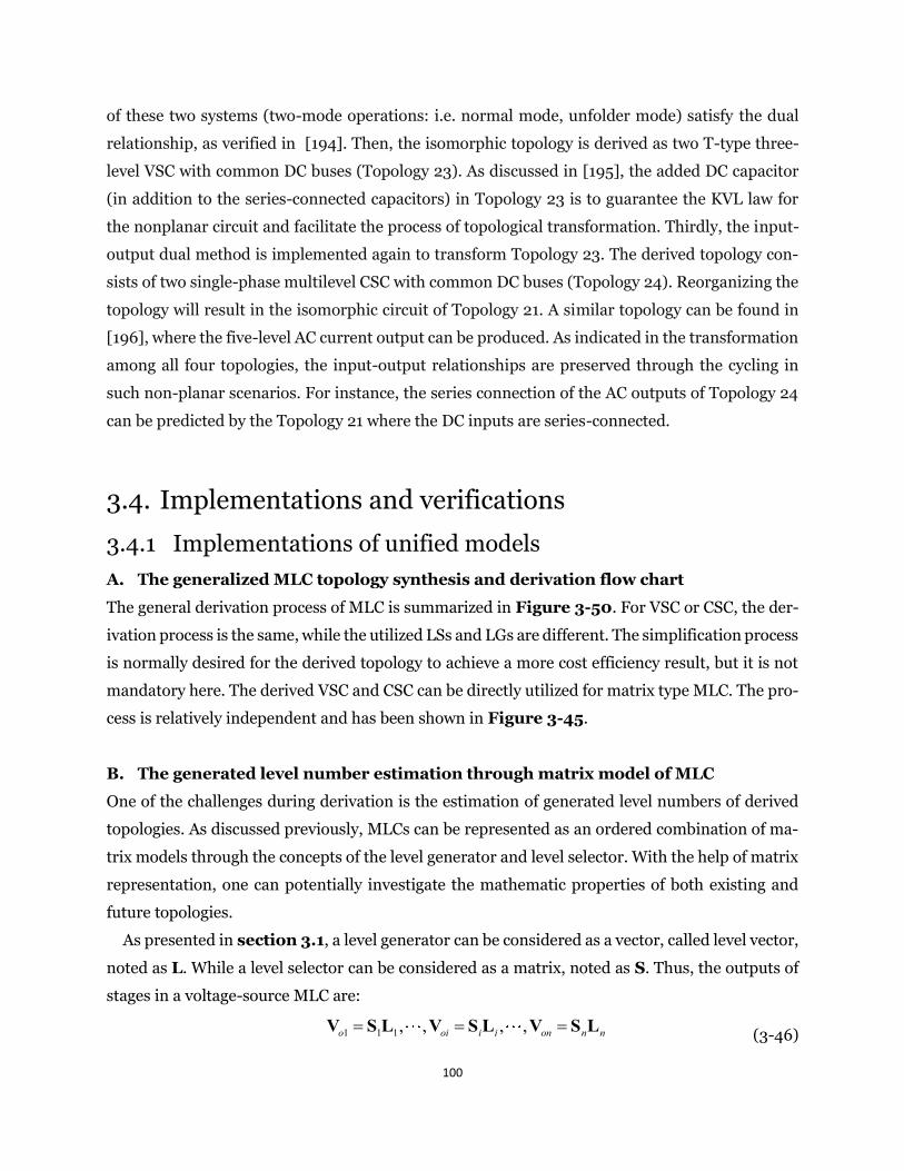
100
of these two systems (two-mode operations: i.e. normal mode, unfolder mode) satisfy the dual
relationship, as verified in [194]. Then, the isomorphic topology is derived as two T-type three-
level VSC with common DC buses (Topology 23). As discussed in [195], the added DC capacitor
(in addition to the series-connected capacitors) in Topology 23 is to guarantee the KVL law for
the nonplanar circuit and facilitate the process of topological transformation. Thirdly, the input-
output dual method is implemented again to transform Topology 23. The derived topology con-
sists of two single-phase multilevel CSC with common DC buses (Topology 24). Reorganizing the
topology will result in the isomorphic circuit of Topology 21. A similar topology can be found in
[196], where the five-level AC current output can be produced. As indicated in the transformation
among all four topologies, the input-output relationships are preserved through the cycling in
such non-planar scenarios. For instance, the series connection of the AC outputs of Topology 24
can be predicted by the Topology 21 where the DC inputs are series-connected.
3.4. Implementations and verifications
3.4.1 Implementations of unified models
A. The generalized MLC topology synthesis and derivation flow chart
The general derivation process of MLC is summarized in Figure 3-50. For VSC or CSC, the der-
ivation process is the same, while the utilized LSs and LGs are different. The simplification process
is normally desired for the derived topology to achieve a more cost efficiency result, but it is not
mandatory here. The derived VSC and CSC can be directly utilized for matrix type MLC. The pro-
cess is relatively independent and has been shown in Figure 3-45.
B. The generated level number estimation through matrix model of MLC
One of the challenges during derivation is the estimation of generated level numbers of derived
topologies. As discussed previously, MLCs can be represented as an ordered combination of ma-
trix models through the concepts of the level generator and level selector. With the help of matrix
representation, one can potentially investigate the mathematic properties of both existing and
future topologies.
As presented in section 3.1, a level generator can be considered as a vector, called level vector,
noted as L. While a level selector can be considered as a matrix, noted as S. Thus, the outputs of
stages in a voltage-source MLC are:
1 1 1, , , ,o oi i i on n n= = =V S L V S L V S L (3-46)
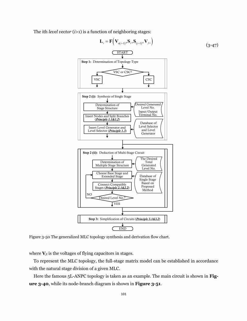
101
The ith level vector (i>1) is a function of neighboring stages:
( ) ( )( )1 1, , ,i i f io i i− −=L F V S S V
(3-47)
Determination of Stage Structure
Insert Nodes and Split Branches (Principle 1.1&1.2)
Insert Level Generator and Level Selector (Principle 1.3)
Database of Level Selector
and Level Generator
START
VSC or CSC?
CSCVSC
Step 2 (i): Synthesis of Single Stage
Step 1: Determination of Topology Type
Step 2 (ii): Deduction of Multi-Stage Circuit
Determination of Multiple Stage Structure
Choose Base Stage and Extended Stage
Connect Compatible Stages (Principle 2.1&2.2)
The Desired Total
Generated Level No.
Database of Single Stage
Based on Proposed Method
Desired Level No.?
YES
NO
Step 3: Simplification of Circuits (Principle 3.1&3.2)
END
Desired Generated Level No.
Input/Output Terminal No.
Figure 3-50 The generalized MLC topology synthesis and derivation flow chart.
where Vfi is the voltages of flying capacitors in stages.
To represent the MLC topology, the full-stage matrix model can be established in accordance
with the natural stage division of a given MLC.
Here the famous 5L-ANPC topology is taken as an example. The main circuit is shown in Fig-
ure 3-40, while its node-branch diagram is shown in Figure 3-51.
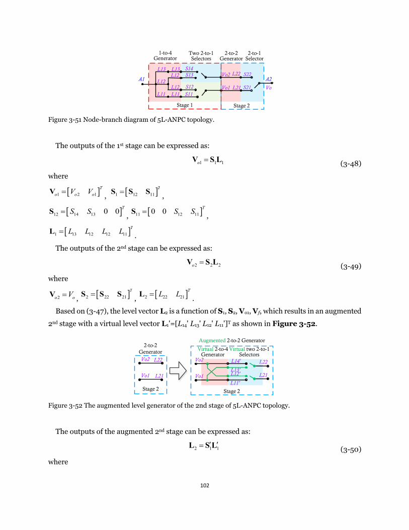
102
A1 A2
L11
L12
L13L22
L21 S21
S22
VoS11S12
S13S14
L11
L12L13
L12
Stage 1
1-to-4 Generator
Two 2-to-1 Selectors
Stage 2
Vo1
Vo2
S21
S22
2-to-2 Generator
2-to-1Selector
Figure 3-51 Node-branch diagram of 5L-ANPC topology.
The outputs of the 1st stage can be expressed as:
1 1 1o =V S L (3-48)
where
1 2 1T
o o oV V=V,
1 12 11T
=S S S,
12 14 13 0 0 TS S=S,
11 12 110 0 TS S=S,
1 13 12 12 11TL L L L=L
.
The outputs of the 2nd stage can be expressed as:
2 2 2o =V S L (3-49)
where
2o oV=V,
2 22 21T
=S S S,
2 22 21TL L=L
.
Based on (3-47), the level vector L2 is a function of S1, S2, Vo1, Vf, which results in an augmented
2nd stage with a virtual level vector L1'=[L14' L13' L12' L11']T as shown in Figure 3-52.
Vo2
Vo1 L21
L22 Vo2
Vo1 L21
L22
L21
L22Vo2
Vo1
2-to-2Generator
Stage 2
Augmented 2-to-2 Generator
Stage 2
Virtual 2-to-4 Generator
Virtual two 2-to-1Selectors
L14'
L13'L12'
L11'
Figure 3-52 The augmented level generator of the 2nd stage of 5L-ANPC topology.
The outputs of the augmented 2nd stage can be expressed as:
2 1 1 =L S L (3-50)
where
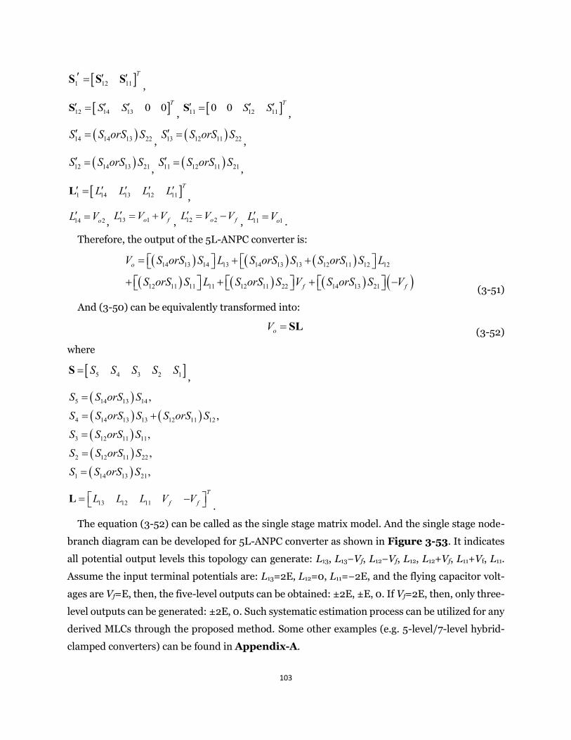
103
1 12 11T =S S S
,
12 14 13 0 0 TS S =S,
11 12 110 0 TS S =S,
( )14 14 13 22S S orS S =,
( )13 12 11 22S S orS S =,
( )12 14 13 21S S orS S =,
( )11 12 11 21S S orS S =,
1 14 13 12 11TL L L L =L
,
14 2oL V =, 13 1o fL V V = +
, 12 2o fL V V = −, 11 1oL V =
.
Therefore, the output of the 5L-ANPC converter is:
( ) ( ) ( )
( ) ( ) ( ) ( )14 13 14 13 14 13 13 12 11 12 12
12 11 11 11 12 11 22 14 13 21
o
f f
V S orS S L S orS S S orS S L
S orS S L S orS S V S orS S V
= + +
+ + + − (3-51)
And (3-50) can be equivalently transformed into:
oV = SL (3-52)
where
5 4 3 2 1S S S S S=S,
( )
( ) ( )
( )
( )
( )
5 14 13 14
4 14 13 13 12 11 12
3 12 11 11
2 12 11 22
1 14 13 21
,
,
,
,
,
S S orS S
S S orS S S orS S
S S orS S
S S orS S
S S orS S
=
= +
=
=
=
13 12 11
T
f fL L L V V = − L.
The equation (3-52) can be called as the single stage matrix model. And the single stage node-
branch diagram can be developed for 5L-ANPC converter as shown in Figure 3-53. It indicates
all potential output levels this topology can generate: L13, L13−Vf, L12−Vf, L12, L12+Vf, L11+Vf, L11.
Assume the input terminal potentials are: L13=2E, L12=0, L11=−2E, and the flying capacitor volt-
ages are Vf=E, then, the five-level outputs can be obtained: ±2E, ±E, 0. If Vf=2E, then, only three-
level outputs can be generated: ±2E, 0. Such systematic estimation process can be utilized for any
derived MLCs through the proposed method. Some other examples (e.g. 5-level/7-level hybrid-
clamped converters) can be found in Appendix-A.
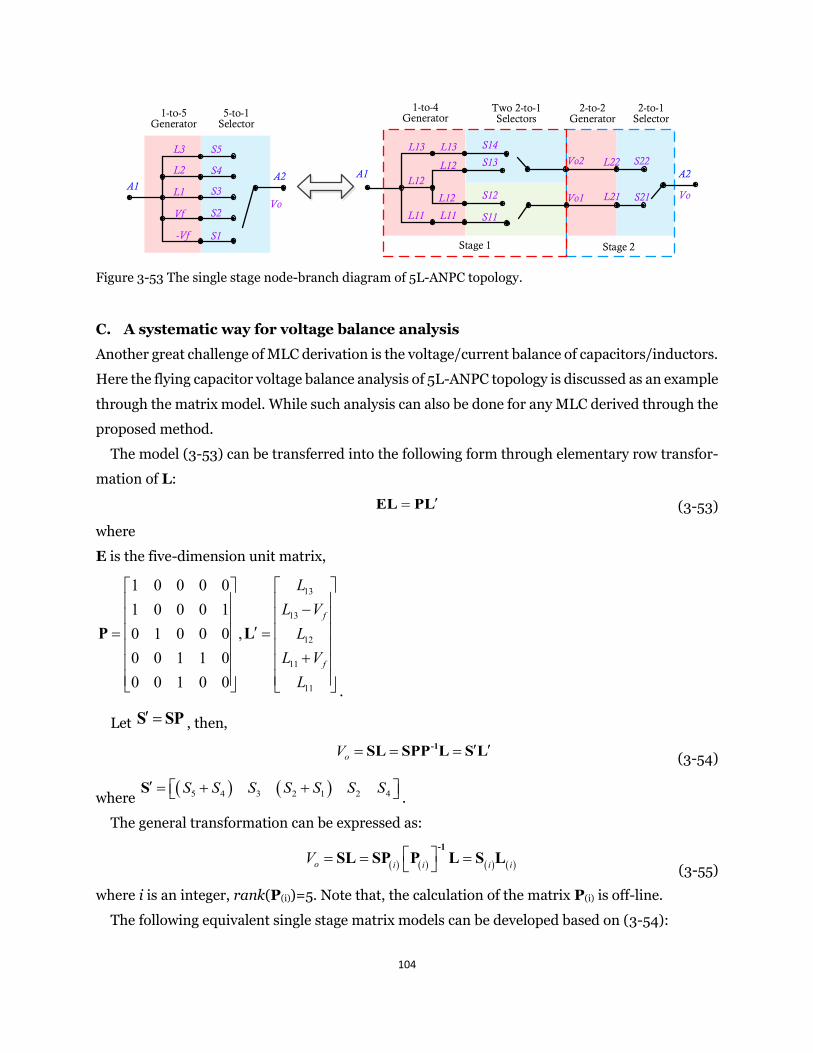
104
1-to-5Generator
A1A2
L1
L2
L3
S2
S3
S4
S5
5-to-1Selector
Vo
S1
Vf
-Vf
A1 A2
L11
L12
L13L22
L21 S21
S22
Vo
S11
S12
S13
S14
L11
L12
L13
L12
Stage 1
1-to-4 Generator
Two 2-to-1 Selectors
Stage 2
Vo1
Vo2
2-to-2 Generator
2-to-1Selector
Figure 3-53 The single stage node-branch diagram of 5L-ANPC topology.
C. A systematic way for voltage balance analysis
Another great challenge of MLC derivation is the voltage/current balance of capacitors/inductors.
Here the flying capacitor voltage balance analysis of 5L-ANPC topology is discussed as an example
through the matrix model. While such analysis can also be done for any MLC derived through the
proposed method.
The model (3-53) can be transferred into the following form through elementary row transfor-
mation of L:
=EL PL (3-53)
where
E is the five-dimension unit matrix,
13
13
12
11
11
1 0 0 0 01 0 0 0 1
,0 1 0 0 00 0 1 1 00 0 1 0 0
f
f
LL V
LL V
L
−
= =
+
P L
.
Let =S SP , then,
oV = = =-1SL SPP L S L (3-54)
where ( ) ( )5 4 3 2 1 2 4S S S S S S S = + + S
.
The general transformation can be expressed as:
( ) ( ) ( ) ( )o i i i iV = = =
-1SL SP P L S L
(3-55)
where i is an integer, rank(P(i))=5. Note that, the calculation of the matrix P(i) is off-line.
The following equivalent single stage matrix models can be developed based on (3-54):
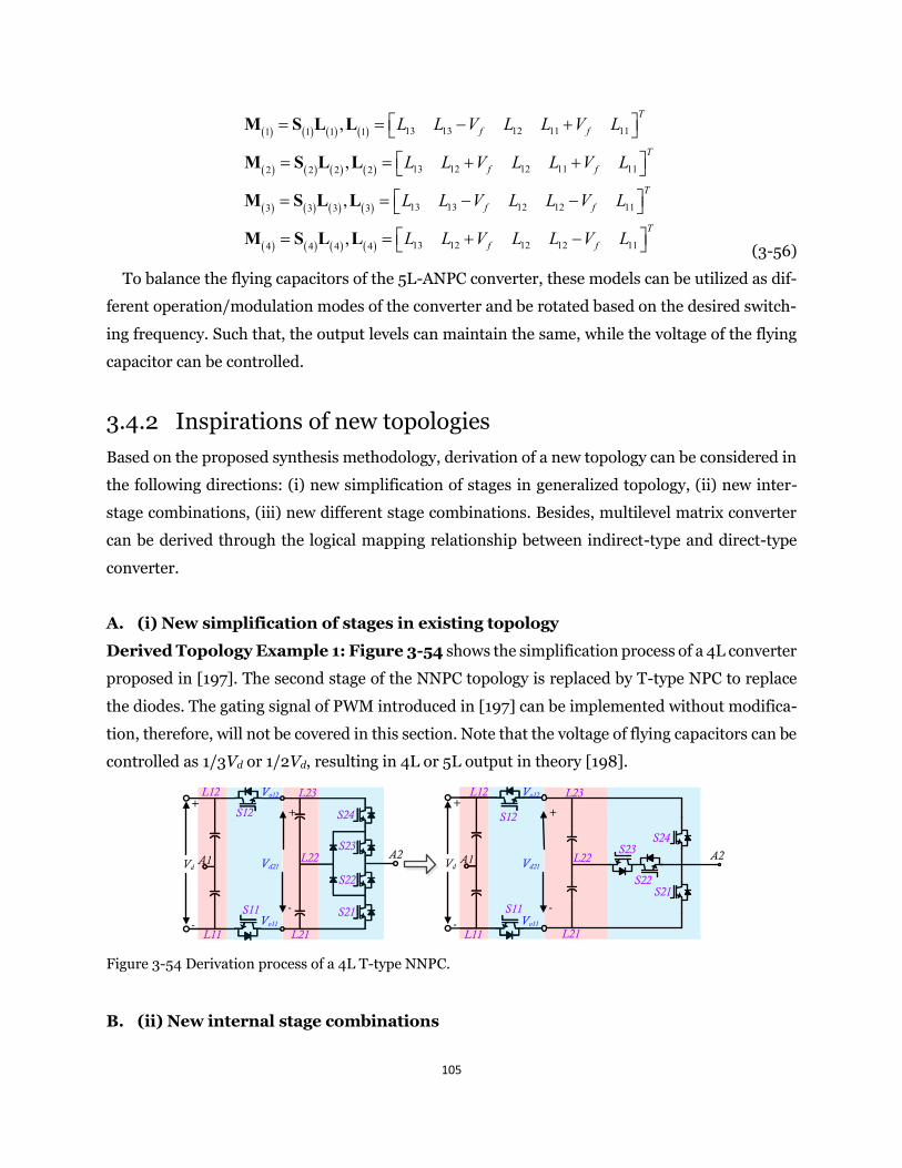
105
( ) ( ) ( ) ( )
( ) ( ) ( ) ( )
( ) ( ) ( ) ( )
( ) ( ) ( ) ( )
13 13 12 11 111 1 1 1
13 12 12 11 112 2 2 2
13 13 12 12 113 3 3 3
13 12 12 12 114 4 4 4
,
,
,
,
T
f f
T
f f
T
f f
T
f f
L L V L L V L
L L V L L V L
L L V L L V L
L L V L L V L
= = − +
= = + +
= = − −
= = + −
M
M
S L L
S L L
S L L
M
M S L L (3-56)
To balance the flying capacitors of the 5L-ANPC converter, these models can be utilized as dif-
ferent operation/modulation modes of the converter and be rotated based on the desired switch-
ing frequency. Such that, the output levels can maintain the same, while the voltage of the flying
capacitor can be controlled.
3.4.2 Inspirations of new topologies
Based on the proposed synthesis methodology, derivation of a new topology can be considered in
the following directions: (i) new simplification of stages in generalized topology, (ii) new inter-
stage combinations, (iii) new different stage combinations. Besides, multilevel matrix converter
can be derived through the logical mapping relationship between indirect-type and direct-type
converter.
A. (i) New simplification of stages in existing topology
Derived Topology Example 1: Figure 3-54 shows the simplification process of a 4L converter
proposed in [197]. The second stage of the NNPC topology is replaced by T-type NPC to replace
the diodes. The gating signal of PWM introduced in [197] can be implemented without modifica-
tion, therefore, will not be covered in this section. Note that the voltage of flying capacitors can be
controlled as 1/3Vd or 1/2Vd, resulting in 4L or 5L output in theory [198].
Vd
+
-
A2A1
+
A1 Vd
+
-
A1
+
A1 A2
+
-
S12
S11
L12
L11
Vd21
Vo12
Vo11
L23
L21
L22
S22
S21
S23
S24 +
-
S12
S11
L12
L11
Vd21
Vo12
Vo11
L23
L21
L22
S22S21
S23S24
Figure 3-54 Derivation process of a 4L T-type NNPC.
B. (ii) New internal stage combinations
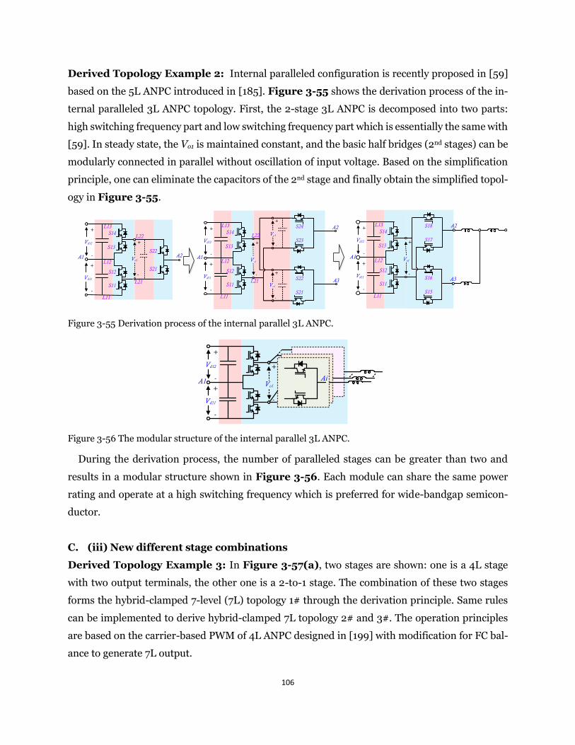
106
Derived Topology Example 2: Internal paralleled configuration is recently proposed in [59]
based on the 5L ANPC introduced in [185]. Figure 3-55 shows the derivation process of the in-
ternal paralleled 3L ANPC topology. First, the 2-stage 3L ANPC is decomposed into two parts:
high switching frequency part and low switching frequency part which is essentially the same with
[59]. In steady state, the Vo1 is maintained constant, and the basic half bridges (2nd stages) can be
modularly connected in parallel without oscillation of input voltage. Based on the simplification
principle, one can eliminate the capacitors of the 2nd stage and finally obtain the simplified topol-
ogy in Figure 3-55.
Vd12
+
-
Vd11
+
-
A2
A2
+
-
Vo1
Vd12
+
-
Vd11
+
-
A2+
-
+
-
Vo1
Vo1
A1 A1
A3
+
-
Vo1
A3
+
-
+
-
VoVoV 1
VoVoV 1
+
-
VoVoV 1
Vd12
+
-
Vd11
+
-
A1
+
-
Vo1
S14
S12
S11
L12
L11
L13
S13
L22
L21
S22
S21
S14
S12
S11
L12
L11
L13
S13
L22
L21
S24
S23
S22
S21
S14
S12
S11
L12
L11
L13
S13
S18
S17
S16
S15
Figure 3-55 Derivation process of the internal parallel 3L ANPC.
Vd12
+
-
Vd11
+
-
A1
+
-
Vo1
Ai
Figure 3-56 The modular structure of the internal parallel 3L ANPC.
During the derivation process, the number of paralleled stages can be greater than two and
results in a modular structure shown in Figure 3-56. Each module can share the same power
rating and operate at a high switching frequency which is preferred for wide-bandgap semicon-
ductor.
C. (iii) New different stage combinations
Derived Topology Example 3: In Figure 3-57(a), two stages are shown: one is a 4L stage
with two output terminals, the other one is a 2-to-1 stage. The combination of these two stages
forms the hybrid-clamped 7-level (7L) topology 1# through the derivation principle. Same rules
can be implemented to derive hybrid-clamped 7L topology 2# and 3#. The operation principles
are based on the carrier-based PWM of 4L ANPC designed in [199] with modification for FC bal-
ance to generate 7L output.
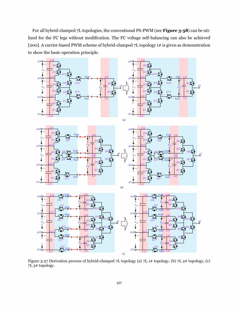
107
For all hybrid-clamped 7L topologies, the conventional PS-PWM (see Figure 3-58) can be uti-
lized for the FC legs without modification. The FC voltage self-balancing can also be achieved
[200]. A carrier-based PWM scheme of hybrid-clamped 7L topology 1# is given as demonstration
to show the basic operation principle.
Vd12
+
-
Vd11
+
-
A2
A13+
-
Vd21
A14
A12+
-A11
S110
S19
S18
S17Vo21
Vo22
S16
S15
S14
S13
S12
S11
L12
L11
L13
L14
L22
L21
S22
S21
S112
S111
Vd12
+
-
Vd11
+
-
A2
A13+
-
Vd21
A14
A12+
-A11
S110
S19
S18
S17Vo21
Vo22
S16
S15
S14
S13
S12
S11
L12
L11
L13
L14
L22
L21
S22
S21
S112
S111
(a)
Vd12
+
-
Vd11
+
-
A13
+
-
Vd22
A14
A12+
-A11
S16
S15
S14
S13
S12
S11
L12
L11
L13
L14
L24
L23
S24
S23
Vo22
Vo24
Vo21
+
-
Vd21
L22
L21
S22
S21
S26
S25
A2
S17
S19
S20
Vo23
S18
Vd12
+
-
Vd11
+
-
A13
+
-
Vd22
A14
A12+
-A11
S16
S15
S14
S13
S12
S11
L12
L11
L13
L14
L24
L23
S24
S23
Vo22
Vo24
Vo21
+
-
Vd21
L22
L21
S22
S21
S26
S25
A2
S17
S19
S20
Vo23
S18
(b)
Vd12
+
-
Vd11
+
-
A13
+
-
Vd23
A14
A12+
-A11
S16
S15
S14
S12
S11
L12
L11
L13
L14 L26
L25
S26
S25
Vo26
Vo25
Vo24
Vo23
Vo21
Vo22
+
-
Vd22
L24
L23
S24
S23S13
+
-
Vd21
L22
L21
S22
S21
A2
S28
S27
S210
S29S212
S211
Vd12
+
-
Vd11
+
-
A13
+
-
Vd23
A14
A12+
-A11
S16
S15
S14
S12
S11
L12
L11
L13
L14 L26
L25
S26
S25
Vo26
Vo25
Vo24
Vo23
Vo21
Vo22
+
-
Vd22
L24
L23
S24
S23S13
+
-
Vd21
L22
L21
S22
S21
A2
S28
S27
S210
S29S212
S211
(c) Figure 3-57 Derivation process of hybrid-clamped 7L topology (a) 7L 1# topology, (b) 7L 2# topology, (c) 7L 3# topology.
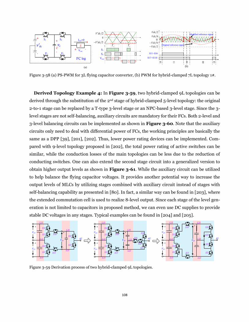
108
2Vdc
06Vdc
2Vdc−
6Vdc−
Modified reference signal
Original reference signal
01 11 01 00 01
S11~S16
S17~S110
S1
Vout
S2
C+
C-
C-
C+
C-
C-
2V dc0
2V dc−
sT sT
S1
S 1
S2
S 2
CZv'dc vc
Vout+ -
+
-
+
-
Iout>0
FC leg
(a) (b) Figure 3-58 (a) PS-PWM for 3L flying capacitor converter, (b) PWM for hybrid-clamped 7L topology 1#.
Derived Topology Example 4: In Figure 3-59, two hybrid-clamped 9L topologies can be
derived through the substitution of the 2nd stage of hybrid-clamped 5-level topology: the original
2-to-1 stage can be replaced by a T-type 3-level stage or an NPC-based 3-level stage. Since the 3-
level stages are not self-balancing, auxiliary circuits are mandatory for their FCs. Both 2-level and
3-level balancing circuits can be implemented as shown in Figure 3-60. Note that the auxiliary
circuits only need to deal with differential power of FCs, the working principles are basically the
same as a DPP [39], [201], [202]. Thus, lower power rating devices can be implemented. Com-
pared with 9-level topology proposed in [202], the total power rating of active switches can be
similar, while the conduction losses of the main topologies can be less due to the reduction of
conducting switches. One can also extend the second stage circuit into a generalized version to
obtain higher output levels as shown in Figure 3-61. While the auxiliary circuit can be utilized
to help balance the flying capacitor voltages. It provides another potential way to increase the
output levels of MLCs by utilizing stages combined with auxiliary circuit instead of stages with
self-balancing capability as presented in [80]. In fact, a similar way can be found in [203], where
the extended commutation cell is used to realize 8-level output. Since each stage of the level gen-
eration is not limited to capacitors in proposed method, we can even use DC supplies to provide
stable DC voltages in any stages. Typical examples can be found in [204] and [205].
Vd12
+
-
Vd11
+
-
A2
+
-
Vd21A2
L23
L21
L22
S22
S21
S23
S24Vd12
+
-
Vd11
+
-
+
-
Vd21
L13
L11
L12
S11
S12
S13
S14
S15
S16
L13
L11
L12
S11
S12
S13
S14
S15
S16
L21
L22
S22
S21
Vd12
+
-
Vd11
+
-
L13
L11
L12
S11
S12
S13
S14
S15
S16
L23
L21
L22
S22
S21
S23
S24+
-
Vd21
A2
Figure 3-59 Derivation process of two hybrid-clamped 9L topologies.
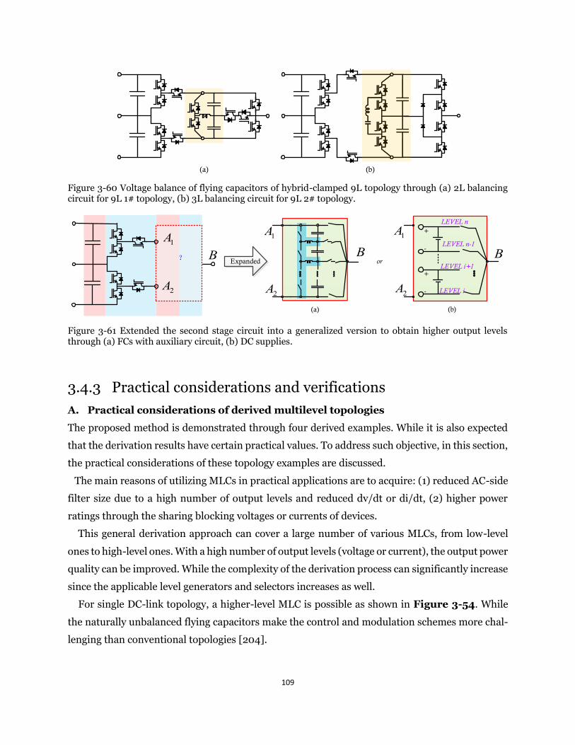
109
(a) (b) Figure 3-60 Voltage balance of flying capacitors of hybrid-clamped 9L topology through (a) 2L balancing circuit for 9L 1# topology, (b) 3L balancing circuit for 9L 2# topology.
Expanded
1A
2A
B? orLEVEL i+1
+
- LEVEL i
LEVEL n+
-LEVEL n-1
1A
2A
B1A
2A
B
(a) (b) Figure 3-61 Extended the second stage circuit into a generalized version to obtain higher output levels through (a) FCs with auxiliary circuit, (b) DC supplies.
3.4.3 Practical considerations and verifications
A. Practical considerations of derived multilevel topologies
The proposed method is demonstrated through four derived examples. While it is also expected
that the derivation results have certain practical values. To address such objective, in this section,
the practical considerations of these topology examples are discussed.
The main reasons of utilizing MLCs in practical applications are to acquire: (1) reduced AC-side
filter size due to a high number of output levels and reduced dv/dt or di/dt, (2) higher power
ratings through the sharing blocking voltages or currents of devices.
This general derivation approach can cover a large number of various MLCs, from low-level
ones to high-level ones. With a high number of output levels (voltage or current), the output power
quality can be improved. While the complexity of the derivation process can significantly increase
since the applicable level generators and selectors increases as well.
For single DC-link topology, a higher-level MLC is possible as shown in Figure 3-54. While
the naturally unbalanced flying capacitors make the control and modulation schemes more chal-
lenging than conventional topologies [204].
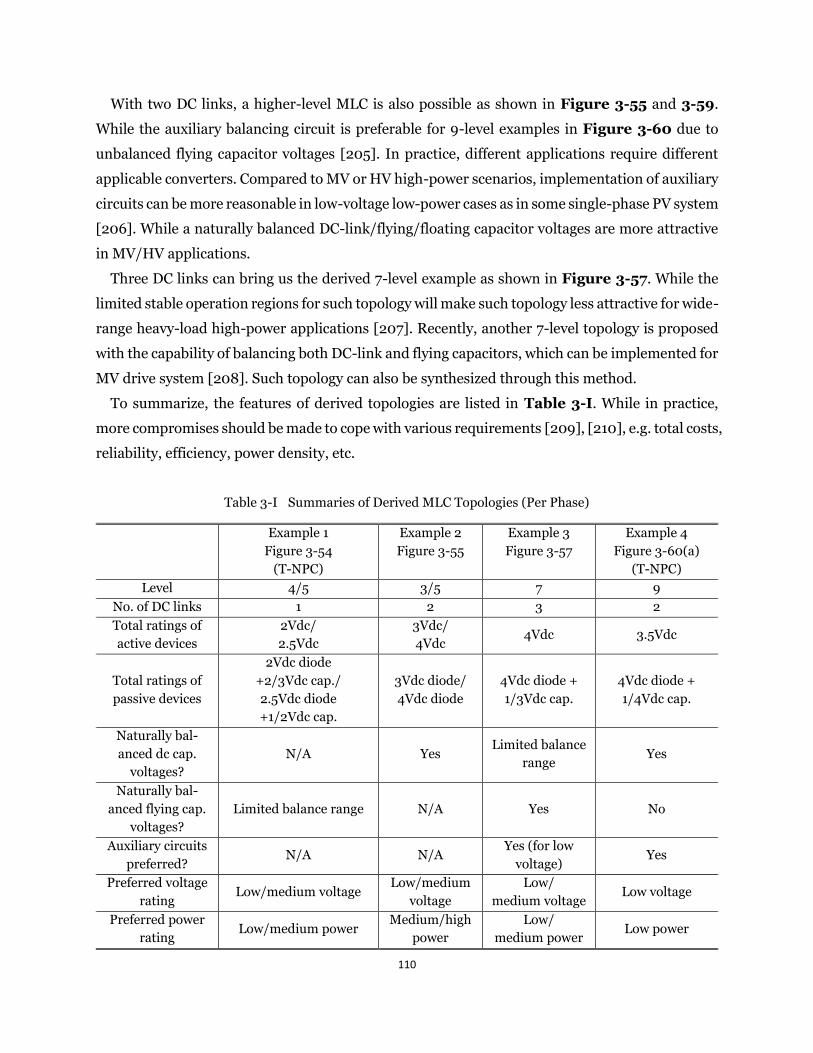
110
With two DC links, a higher-level MLC is also possible as shown in Figure 3-55 and 3-59.
While the auxiliary balancing circuit is preferable for 9-level examples in Figure 3-60 due to
unbalanced flying capacitor voltages [205]. In practice, different applications require different
applicable converters. Compared to MV or HV high-power scenarios, implementation of auxiliary
circuits can be more reasonable in low-voltage low-power cases as in some single-phase PV system
[206]. While a naturally balanced DC-link/flying/floating capacitor voltages are more attractive
in MV/HV applications.
Three DC links can bring us the derived 7-level example as shown in Figure 3-57. While the
limited stable operation regions for such topology will make such topology less attractive for wide-
range heavy-load high-power applications [207]. Recently, another 7-level topology is proposed
with the capability of balancing both DC-link and flying capacitors, which can be implemented for
MV drive system [208]. Such topology can also be synthesized through this method.
To summarize, the features of derived topologies are listed in Table 3-I. While in practice,
more compromises should be made to cope with various requirements [209], [210], e.g. total costs,
reliability, efficiency, power density, etc.
Table 3-I Summaries of Derived MLC Topologies (Per Phase)
Example 1
Figure 3-54
(T-NPC)
Example 2
Figure 3-55
Example 3
Figure 3-57
Example 4
Figure 3-60(a)
(T-NPC)
Level 4/5 3/5 7 9
No. of DC links 1 2 3 2
Total ratings of
active devices
2Vdc/
2.5Vdc
3Vdc/
4Vdc 4Vdc 3.5Vdc
Total ratings of
passive devices
2Vdc diode
+2/3Vdc cap./
2.5Vdc diode
+1/2Vdc cap.
3Vdc diode/
4Vdc diode
4Vdc diode +
1/3Vdc cap.
4Vdc diode +
1/4Vdc cap.
Naturally bal-
anced dc cap.
voltages?
N/A Yes Limited balance
range Yes
Naturally bal-
anced flying cap.
voltages?
Limited balance range N/A Yes No
Auxiliary circuits
preferred? N/A N/A
Yes (for low
voltage) Yes
Preferred voltage
rating Low/medium voltage
Low/medium
voltage
Low/
medium voltage Low voltage
Preferred power
rating Low/medium power
Medium/high
power
Low/
medium power Low power
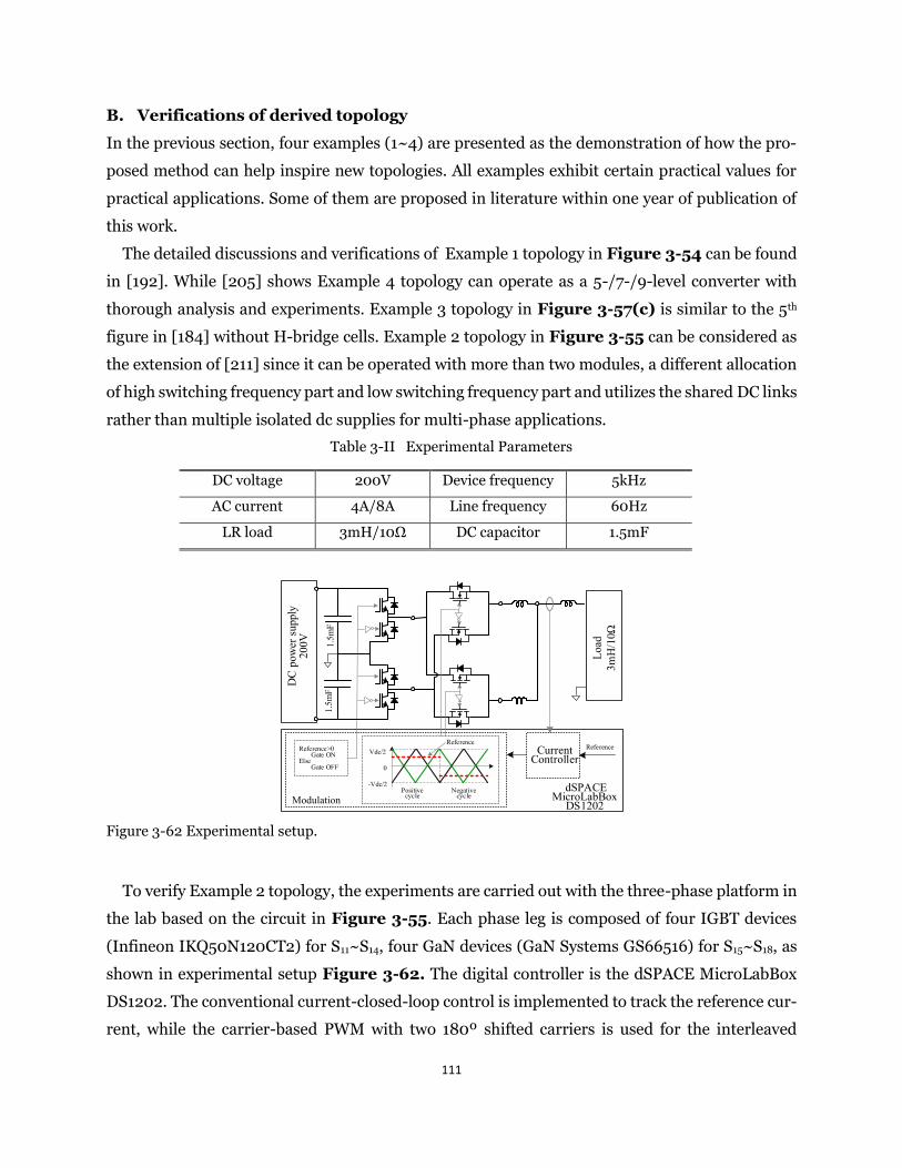
111
B. Verifications of derived topology
In the previous section, four examples (1~4) are presented as the demonstration of how the pro-
posed method can help inspire new topologies. All examples exhibit certain practical values for
practical applications. Some of them are proposed in literature within one year of publication of
this work.
The detailed discussions and verifications of Example 1 topology in Figure 3-54 can be found
in [192]. While [205] shows Example 4 topology can operate as a 5-/7-/9-level converter with
thorough analysis and experiments. Example 3 topology in Figure 3-57(c) is similar to the 5th
figure in [184] without H-bridge cells. Example 2 topology in Figure 3-55 can be considered as
the extension of [211] since it can be operated with more than two modules, a different allocation
of high switching frequency part and low switching frequency part and utilizes the shared DC links
rather than multiple isolated dc supplies for multi-phase applications.
Table 3-II Experimental Parameters
DC voltage 200V Device frequency 5kHz
AC current 4A/8A Line frequency 60Hz
LR load 3mH/10Ω DC capacitor 1.5mF
DC
pow
er su
pply
20
0V
Positive cycle
Negative cycle
0
Vdc/2
-Vdc/2 dSPACE MicroLabBox
DS1202
1.5m
F1.
5mF
Load
3mH
/10Ω
Reference>0 Gate ONElse Gate OFF
Reference
Modulation
Current Controller
Reference
Figure 3-62 Experimental setup.
To verify Example 2 topology, the experiments are carried out with the three-phase platform in
the lab based on the circuit in Figure 3-55. Each phase leg is composed of four IGBT devices
(Infineon IKQ50N120CT2) for S11~S14, four GaN devices (GaN Systems GS66516) for S15~S18, as
shown in experimental setup Figure 3-62. The digital controller is the dSPACE MicroLabBox
DS1202. The conventional current-closed-loop control is implemented to track the reference cur-
rent, while the carrier-based PWM with two 180º shifted carriers is used for the interleaved
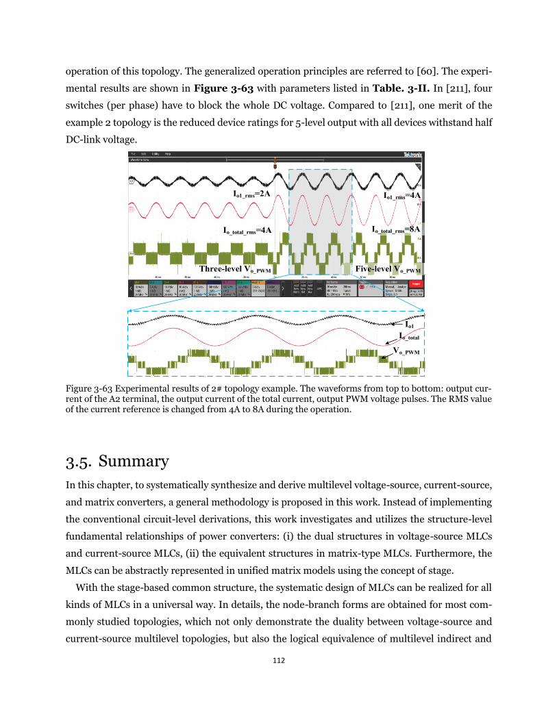
112
operation of this topology. The generalized operation principles are referred to [60]. The experi-
mental results are shown in Figure 3-63 with parameters listed in Table. 3-II. In [211], four
switches (per phase) have to block the whole DC voltage. Compared to [211], one merit of the
example 2 topology is the reduced device ratings for 5-level output with all devices withstand half
DC-link voltage.
Io1
Io_total
Vo_PWM
Io1_rms=2A Io1_rms=4A
Io_total_rms=4A Io_total_rms=8A
Three-level Vo_PWM Five-level Vo_PWM
Figure 3-63 Experimental results of 2# topology example. The waveforms from top to bottom: output cur-rent of the A2 terminal, the output current of the total current, output PWM voltage pulses. The RMS value of the current reference is changed from 4A to 8A during the operation.
3.5. Summary
In this chapter, to systematically synthesize and derive multilevel voltage-source, current-source,
and matrix converters, a general methodology is proposed in this work. Instead of implementing
the conventional circuit-level derivations, this work investigates and utilizes the structure-level
fundamental relationships of power converters: (i) the dual structures in voltage-source MLCs
and current-source MLCs, (ii) the equivalent structures in matrix-type MLCs. Furthermore, the
MLCs can be abstractly represented in unified matrix models using the concept of stage.
With the stage-based common structure, the systematic design of MLCs can be realized for all
kinds of MLCs in a universal way. In details, the node-branch forms are obtained for most com-
monly studied topologies, which not only demonstrate the duality between voltage-source and
current-source multilevel topologies, but also the logical equivalence of multilevel indirect and
113
direct matrix converters. The matrix presentations of MLCs are derived from their node-branch
forms, which provides an opportunity for systematic analysis of different MLCs. It can help the
simplification process of derived various MLC topologies, and can also facilitate the modulation
implementation for different MLCs, especially matrix converters, through the logic mapping.
Moreover, compared to the current approach of manual design and analysis, the design rules
of the proposed method are more general and straightforward to follow even for researchers with-
out a strong power electronics background. With the proposed method, a unified design platform
could be established, which opens the potential for both manual synthesis and derivation and
computer-aided design and analysis. Several multilevel topologies are derived as examples, e.g.
internal paralleled MLCs, 7L hybrid MLCs and 9L MLCs with auxiliary circuits. The discussions
with practical considerations and experiments are given to further demonstrate the feasibility of
the proposed method.
As briefly mentioned in Section 3.4, the matrix models introduced in this chapter can also be
utilized for topology simplification and modulation of MLCs. In the following Chapter 5, this
concept will be further generalized and implemented for those MLCs with non-modular structures,
e.g. ANPC-type converters. Those topologies have been facing some great challenges of modula-
tion implementation when dealing with topology simplification and fault-tolerant operation. With
the help of some specialized matrix modeling approaches, both can be solved in systematic ways.
114
Chapter 4 Systematic PWM design of multilevel
converters1
As reviewed in Chapter 1, the maturity of power electronic techniques drives the converter per-
formance approaching its limitations. To fully explore the potentials of various MLCs and estab-
lish the common database, not only the topology synthesis method is highly needed (as investi-
gated in Chapter 3), but also the modulation design needs to be systematically addressed. Un-
fortunately, the systematic PWM design methods are still hardly discussed in literature. Consid-
erable efforts have been dedicated for modulation design of some three-level MLCs, such as loss
distribution improvement, thermal management, commutation and fault-tolerant modulations
[97], [212]-[216]. For MLCs with modular structures (e.g. CHB, MMC, FC converters), these
methods could be systematically generalized for higher output level scenarios. However, due to
the complex circuit structures, it is more difficult to design modulations for the non-modular
MLCs, e.g. NPC, ANPC, hybrid-clamped converters. In fact, most of the non-modular MLCs can
be simplified or extended by ANPC-type converters, which will be considered in this chapter.
In practice, the ANPC converter is one of the most typical non-modular MLCs and has been
drawing considerable attention in recent MLC research as mentioned in Chapter 1. By providing
more redundancies, the ANPC converter has a higher flexibility than NPC converter and can po-
tentially achieve better performance. It can also be generalized into various other MLCs by adding
flying capacitors by substituting the certain switching cells or simplifying the circuit (e.g. hybrid-
clamped converters). With some clear derivation rules (such as those in Chapter 3), the modu-
lation design of its resulting derivatives can benefit from the established approaches for ANPC
converter. Therefore, in this chapter, the ANPC converter is chosen for the major research subject
to demonstrate the proposed methodology without losing the generality.
1 Publications out of this Chapter:
Yuzhuo Li, Yunwei Li, Hao Tian, Navid R. Zargari and Zhongyuan Cheng, "A Modular Design Approach to Provide Exhaustive Car-rier-Based PWM Patterns for Multilevel ANPC Converters," in IEEE Transactions on Industry Applications, vol. 55, no. 5, pp. 5032-5044, Sept.-Oct. 2019 Yuzhuo Li, Hao Tian and Yunwei Li, "Generalized Phase-Shift PWM for Active-Neutral-Point-Clamped Multilevel Converter," in IEEE Transactions on Industrial Electronics, vol. 67, no. 11, pp. 9048-9058, Nov. 2020. Yuzhuo Li, Yunwei Li and Hao Tian, "Carrier-based PWM design of multilevel ANPC-based converter through hierarchical decom-position," 2018 IEEE Applied Power Electronics Conference and Exposition (APEC), San Antonio, TX, 2018, pp. 2542-2549.
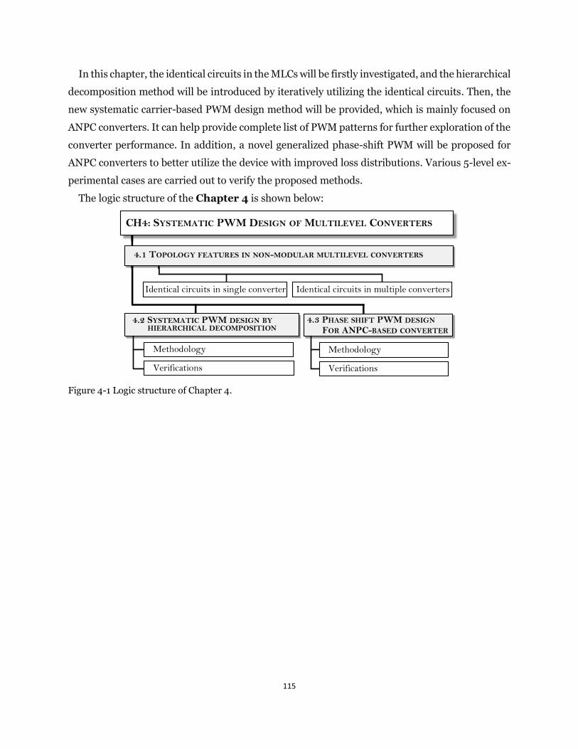
115
In this chapter, the identical circuits in the MLCs will be firstly investigated, and the hierarchical
decomposition method will be introduced by iteratively utilizing the identical circuits. Then, the
new systematic carrier-based PWM design method will be provided, which is mainly focused on
ANPC converters. It can help provide complete list of PWM patterns for further exploration of the
converter performance. In addition, a novel generalized phase-shift PWM will be proposed for
ANPC converters to better utilize the device with improved loss distributions. Various 5-level ex-
perimental cases are carried out to verify the proposed methods.
The logic structure of the Chapter 4 is shown below:
CH4: SYSTEMATIC PWM DESIGN OF MULTILEVEL CONVERTERS
4.1 TOPOLOGY FEATURES IN NON-MODULAR MULTILEVEL CONVERTERS
Methodology
Verifications
4.3 PHASE SHIFT PWM DESIGN FOR ANPC-BASED CONVERTER
Methodology
Verifications
4.2 SYSTEMATIC PWM DESIGN BY HIERARCHICAL DECOMPOSITION
Identical circuits in single converter Identical circuits in multiple converters
Figure 4-1 Logic structure of Chapter 4.
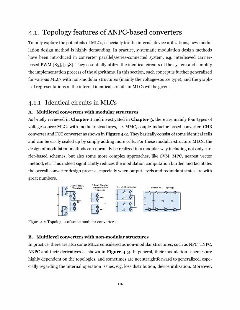
116
4.1. Topology features of ANPC-based converters
To fully explore the potentials of MLCs, especially for the internal device utilizations, new modu-
lation design method is highly demanding. In practice, systematic modulation design methods
have been introduced in converter parallel/series-connected system, e.g. interleaved carrier-
based PWM [85], [158]. They essentially utilize the identical circuits of the system and simplify
the implementation process of the algorithms. In this section, such concept is further generalized
for various MLCs with non-modular structures (mainly the voltage-source type), and the graph-
ical representations of the internal identical circuits in MLCs will be given.
4.1.1 Identical circuits in MLCs
A. Multilevel converters with modular structures
As briefly reviewed in Chapter 1 and investigated in Chapter 3, there are mainly four types of
voltage-source MLCs with modular structures, i.e. MMC, couple-inductor-based converter, CHB
converter and FCC converter as shown in Figure 4-2. They basically consist of some identical cells
and can be easily scaled up by simply adding more cells. For these modular-structure MLCs, the
design of modulation methods can normally be realized in a modular way including not only car-
rier-based schemes, but also some more complex approaches, like SVM, MPC, nearest vector
method, etc. This indeed significantly reduces the modulation computation burden and facilitates
the overall converter design process, especially when output levels and redundant states are with
great numbers.
5-level FCC Topology3-level MMC
Topology 5L CHB converter 3-level Couple-inductor-based
Topology
Figure 4-2 Topologies of some modular converters.
B. Multilevel converters with non-modular structures
In practice, there are also some MLCs considered as non-modular structures, such as NPC, TNPC,
ANPC and their derivatives as shown in Figure 4-3. In general, their modulation schemes are
highly dependent on the topologies, and sometimes are not straightforward to generalized, espe-
cially regarding the internal operation issues, e.g. loss distribution, device utilization. Moreover,
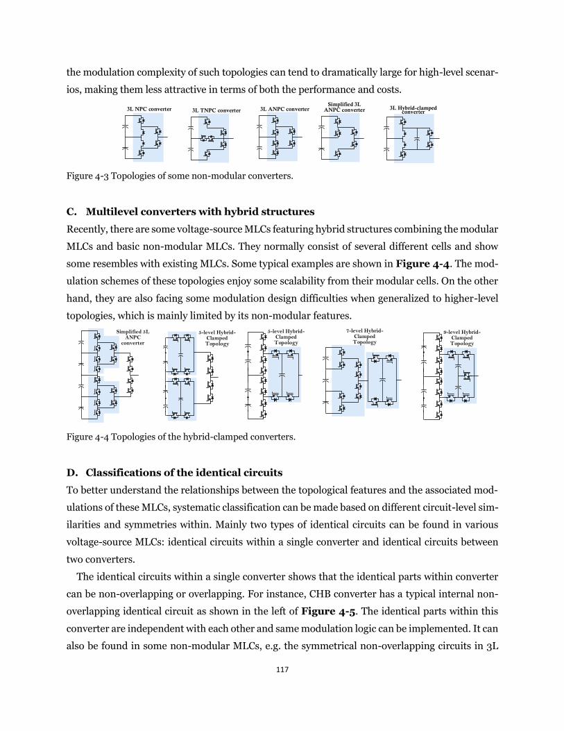
117
the modulation complexity of such topologies can tend to dramatically large for high-level scenar-
ios, making them less attractive in terms of both the performance and costs.
Simplified 3L ANPC converter 3L NPC converter 3L ANPC converter 3L TNPC converter 3L Hybrid-clamped
converter
Figure 4-3 Topologies of some non-modular converters.
C. Multilevel converters with hybrid structures
Recently, there are some voltage-source MLCs featuring hybrid structures combining the modular
MLCs and basic non-modular MLCs. They normally consist of several different cells and show
some resembles with existing MLCs. Some typical examples are shown in Figure 4-4. The mod-
ulation schemes of these topologies enjoy some scalability from their modular cells. On the other
hand, they are also facing some modulation design difficulties when generalized to higher-level
topologies, which is mainly limited by its non-modular features.
5-level Hybrid-Clamped Topology
5-level Hybrid-Clamped Topology
Simplified 5L ANPC
converter
7-level Hybrid-Clamped Topology
9-level Hybrid-Clamped Topology
Figure 4-4 Topologies of the hybrid-clamped converters.
D. Classifications of the identical circuits
To better understand the relationships between the topological features and the associated mod-
ulations of these MLCs, systematic classification can be made based on different circuit-level sim-
ilarities and symmetries within. Mainly two types of identical circuits can be found in various
voltage-source MLCs: identical circuits within a single converter and identical circuits between
two converters.
The identical circuits within a single converter shows that the identical parts within converter
can be non-overlapping or overlapping. For instance, CHB converter has a typical internal non-
overlapping identical circuit as shown in the left of Figure 4-5. The identical parts within this
converter are independent with each other and same modulation logic can be implemented. It can
also be found in some non-modular MLCs, e.g. the symmetrical non-overlapping circuits in 3L
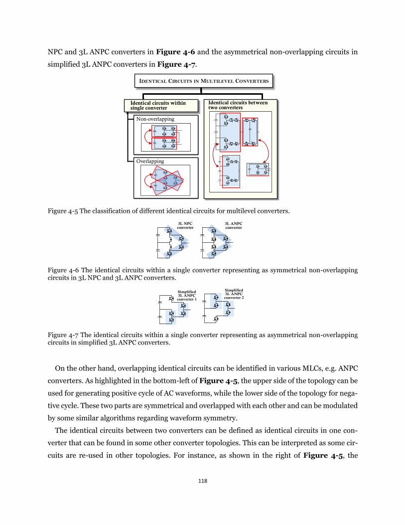
118
NPC and 3L ANPC converters in Figure 4-6 and the asymmetrical non-overlapping circuits in
simplified 3L ANPC converters in Figure 4-7.
Non-overlapping
Overlapping
IDENTICAL CIRCUITS IN MULTILEVEL CONVERTERS
Identical circuits within single converter
Identical circuits between two converters
Figure 4-5 The classification of different identical circuits for multilevel converters.
3L NPC converter
3L ANPC converter
Figure 4-6 The identical circuits within a single converter representing as symmetrical non-overlapping circuits in 3L NPC and 3L ANPC converters.
Simplified 3L ANPC converter 2
Simplified 3L ANPC converter 1
Figure 4-7 The identical circuits within a single converter representing as asymmetrical non-overlapping circuits in simplified 3L ANPC converters.
On the other hand, overlapping identical circuits can be identified in various MLCs, e.g. ANPC
converters. As highlighted in the bottom-left of Figure 4-5, the upper side of the topology can be
used for generating positive cycle of AC waveforms, while the lower side of the topology for nega-
tive cycle. These two parts are symmetrical and overlapped with each other and can be modulated
by some similar algorithms regarding waveform symmetry.
The identical circuits between two converters can be defined as identical circuits in one con-
verter that can be found in some other converter topologies. This can be interpreted as some cir-
cuits are re-used in other topologies. For instance, as shown in the right of Figure 4-5, the
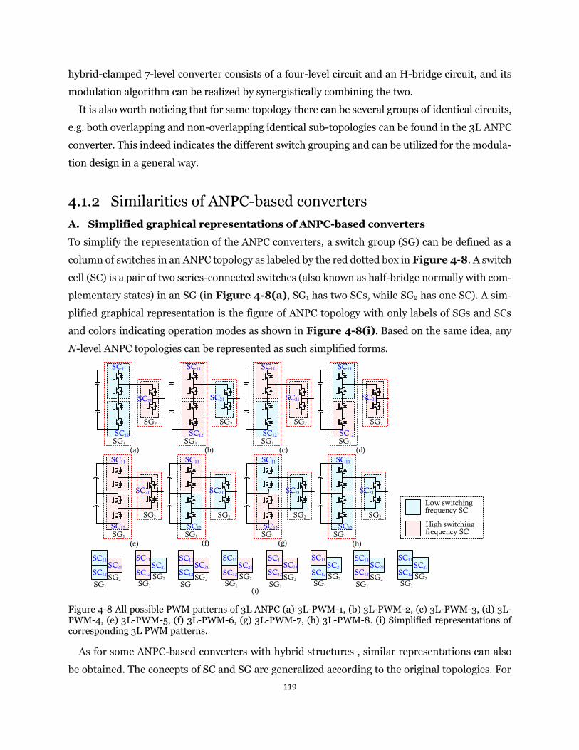
119
hybrid-clamped 7-level converter consists of a four-level circuit and an H-bridge circuit, and its
modulation algorithm can be realized by synergistically combining the two.
It is also worth noticing that for same topology there can be several groups of identical circuits,
e.g. both overlapping and non-overlapping identical sub-topologies can be found in the 3L ANPC
converter. This indeed indicates the different switch grouping and can be utilized for the modula-
tion design in a general way.
4.1.2 Similarities of ANPC-based converters
A. Simplified graphical representations of ANPC-based converters
To simplify the representation of the ANPC converters, a switch group (SG) can be defined as a
column of switches in an ANPC topology as labeled by the red dotted box in Figure 4-8. A switch
cell (SC) is a pair of two series-connected switches (also known as half-bridge normally with com-
plementary states) in an SG (in Figure 4-8(a), SG1 has two SCs, while SG2 has one SC). A sim-
plified graphical representation is the figure of ANPC topology with only labels of SGs and SCs
and colors indicating operation modes as shown in Figure 4-8(i). Based on the same idea, any
N-level ANPC topologies can be represented as such simplified forms.
SG2
SC12
SC21
SG1
SC11
(b)(a) (c) (d)
(e)
SG2
SC12
SC21
SG1
SC11
SG2
SC12
SC21
SG1
SC11
SG2
SC12
SC21
SG1
SC11
SG2
SC12
SC21
SG1
SC11
SG2
SC12
SC21
SG1
SC11
SG2
SC12
SC21
SG1
SC11
SG2
SC12
SC21
SG1
SC11
(f) (g) (h)
Low switching frequency SC
High switching frequency SC
SG1
SG2
SC11
SC12
SC21
SG1
SG2SC12
SC21
SC11
SG1
SG2
SC11
SC12
SC21
SG1
SG2SC12
SC21
SC11
SG1
SG2
SC11
SC12
SC21
SG1
SG2SC12
SC21
SC11
SG1
SG2
SC11
SC12
SC21
SG1
SG2SC12
SC21
SC11
(i)
Figure 4-8 All possible PWM patterns of 3L ANPC (a) 3L-PWM-1, (b) 3L-PWM-2, (c) 3L-PWM-3, (d) 3L-PWM-4, (e) 3L-PWM-5, (f) 3L-PWM-6, (g) 3L-PWM-7, (h) 3L-PWM-8. (i) Simplified representations of corresponding 3L PWM patterns.
As for some ANPC-based converters with hybrid structures , similar representations can also
be obtained. The concepts of SC and SG are generalized according to the original topologies. For
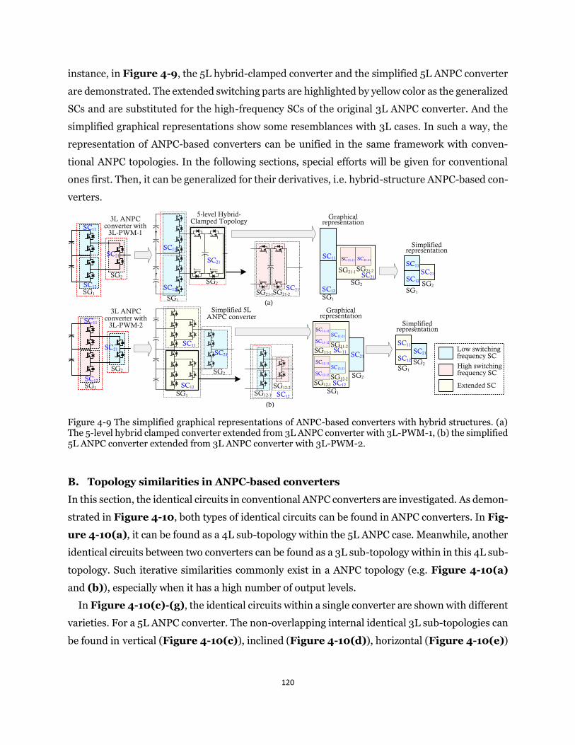
120
instance, in Figure 4-9, the 5L hybrid-clamped converter and the simplified 5L ANPC converter
are demonstrated. The extended switching parts are highlighted by yellow color as the generalized
SCs and are substituted for the high-frequency SCs of the original 3L ANPC converter. And the
simplified graphical representations show some resemblances with 3L cases. In such a way, the
representation of ANPC-based converters can be unified in the same framework with conven-
tional ANPC topologies. In the following sections, special efforts will be given for conventional
ones first. Then, it can be generalized for their derivatives, i.e. hybrid-structure ANPC-based con-
verters.
SG1
SC12
SC11
SC21
SG1
SC12
SC11
SC21
SG2
5-level Hybrid-Clamped Topology
Simplified 5L ANPC converter
(b)
(a)
SG2
SC12SG12-1
SG12-2
SC21SG21-1SG21-2
SG2
SC21
SG1
SC11
SC12
SG11-2SG11-1
SC11-11
SC11-12
SC11-21
SG12-2SG12-1
SC12-11
SC12-12
SC12-21
Graphical representation
SG2
SC21
SG1
SC11
SC12
SG21-1
SC21-11 SC21-21
SG21-2
Graphical representation
SG2
SC21
SG1
SC12
SC11
SG2
SC21
SG1
SC12
SC11
SG2
SC12
SC21
SG1
SC11
SG2
SC12
SC21
SG1
SC11
3L ANPC converter with
3L-PWM-2
3L ANPC converter with
3L-PWM-1
Low switching frequency SC
High switching frequency SC
Extended SC
Simplified representation
Simplified representation
Figure 4-9 The simplified graphical representations of ANPC-based converters with hybrid structures. (a) The 5-level hybrid clamped converter extended from 3L ANPC converter with 3L-PWM-1, (b) the simplified 5L ANPC converter extended from 3L ANPC converter with 3L-PWM-2.
B. Topology similarities in ANPC-based converters
In this section, the identical circuits in conventional ANPC converters are investigated. As demon-
strated in Figure 4-10, both types of identical circuits can be found in ANPC converters. In Fig-
ure 4-10(a), it can be found as a 4L sub-topology within the 5L ANPC case. Meanwhile, another
identical circuits between two converters can be found as a 3L sub-topology within in this 4L sub-
topology. Such iterative similarities commonly exist in a ANPC topology (e.g. Figure 4-10(a)
and (b)), especially when it has a high number of output levels.
In Figure 4-10(c)-(g), the identical circuits within a single converter are shown with different
varieties. For a 5L ANPC converter. The non-overlapping internal identical 3L sub-topologies can
be found in vertical (Figure 4-10(c)), inclined (Figure 4-10(d)), horizontal (Figure 4-10(e))
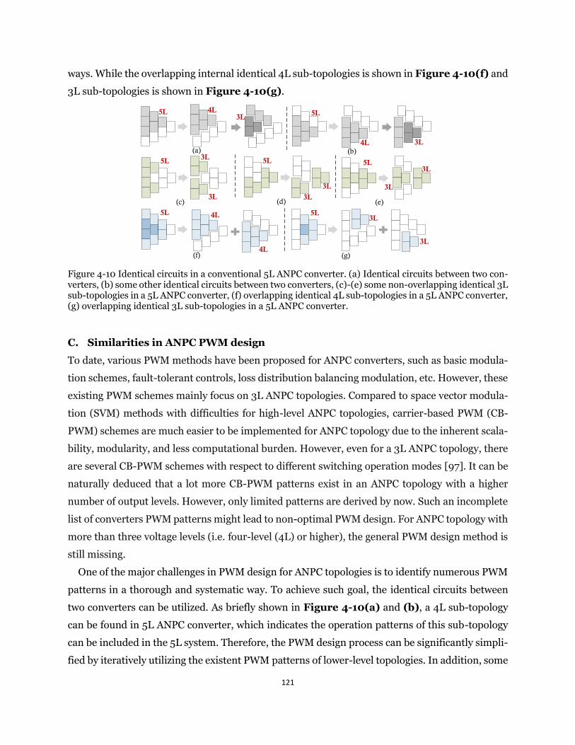
121
ways. While the overlapping internal identical 4L sub-topologies is shown in Figure 4-10(f) and
3L sub-topologies is shown in Figure 4-10(g).
(a) (b)
(c) (d) (e)
5L 4L3L 5L
4L 3L
5L 3L
3L
5L
3L
3L
3L
3L
5L
(g)
5L
(f)
5L 4L
4L
3L
3L
Figure 4-10 Identical circuits in a conventional 5L ANPC converter. (a) Identical circuits between two con-verters, (b) some other identical circuits between two converters, (c)-(e) some non-overlapping identical 3L sub-topologies in a 5L ANPC converter, (f) overlapping identical 4L sub-topologies in a 5L ANPC converter, (g) overlapping identical 3L sub-topologies in a 5L ANPC converter.
C. Similarities in ANPC PWM design
To date, various PWM methods have been proposed for ANPC converters, such as basic modula-
tion schemes, fault-tolerant controls, loss distribution balancing modulation, etc. However, these
existing PWM schemes mainly focus on 3L ANPC topologies. Compared to space vector modula-
tion (SVM) methods with difficulties for high-level ANPC topologies, carrier-based PWM (CB-
PWM) schemes are much easier to be implemented for ANPC topology due to the inherent scala-
bility, modularity, and less computational burden. However, even for a 3L ANPC topology, there
are several CB-PWM schemes with respect to different switching operation modes [97]. It can be
naturally deduced that a lot more CB-PWM patterns exist in an ANPC topology with a higher
number of output levels. However, only limited patterns are derived by now. Such an incomplete
list of converters PWM patterns might lead to non-optimal PWM design. For ANPC topology with
more than three voltage levels (i.e. four-level (4L) or higher), the general PWM design method is
still missing.
One of the major challenges in PWM design for ANPC topologies is to identify numerous PWM
patterns in a thorough and systematic way. To achieve such goal, the identical circuits between
two converters can be utilized. As briefly shown in Figure 4-10(a) and (b), a 4L sub-topology
can be found in 5L ANPC converter, which indicates the operation patterns of this sub-topology
can be included in the 5L system. Therefore, the PWM design process can be significantly simpli-
fied by iteratively utilizing the existent PWM patterns of lower-level topologies. In addition, some
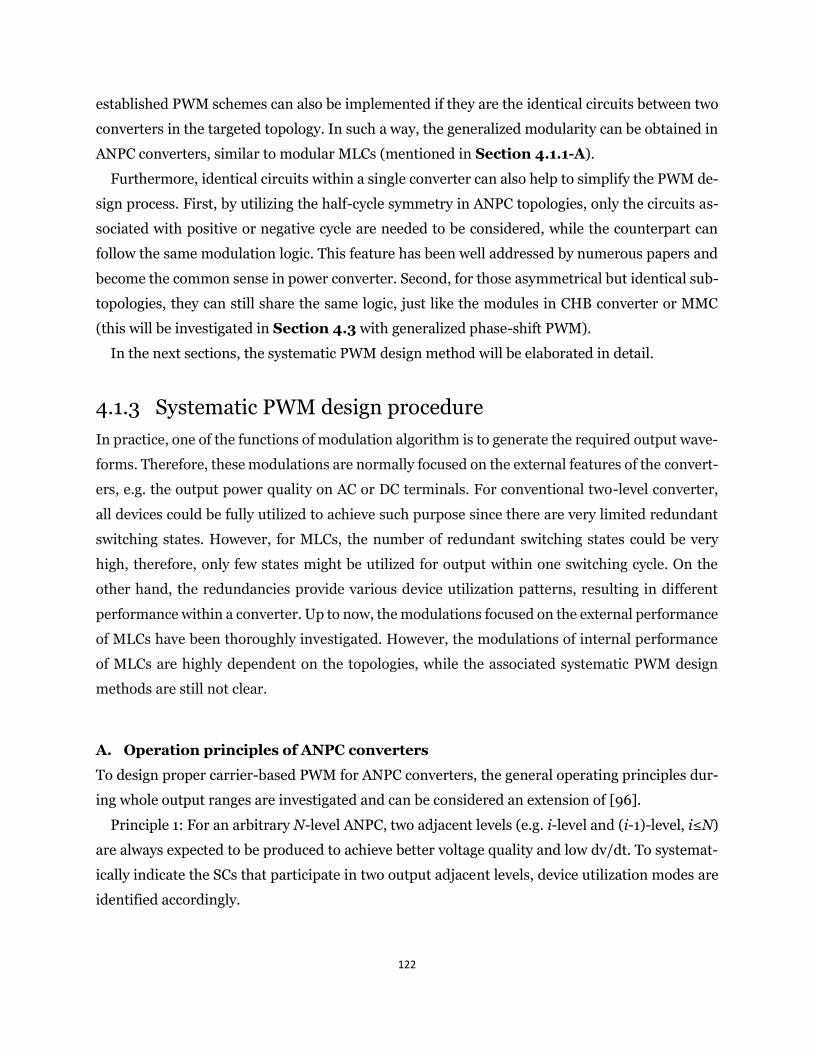
122
established PWM schemes can also be implemented if they are the identical circuits between two
converters in the targeted topology. In such a way, the generalized modularity can be obtained in
ANPC converters, similar to modular MLCs (mentioned in Section 4.1.1-A).
Furthermore, identical circuits within a single converter can also help to simplify the PWM de-
sign process. First, by utilizing the half-cycle symmetry in ANPC topologies, only the circuits as-
sociated with positive or negative cycle are needed to be considered, while the counterpart can
follow the same modulation logic. This feature has been well addressed by numerous papers and
become the common sense in power converter. Second, for those asymmetrical but identical sub-
topologies, they can still share the same logic, just like the modules in CHB converter or MMC
(this will be investigated in Section 4.3 with generalized phase-shift PWM).
In the next sections, the systematic PWM design method will be elaborated in detail.
4.1.3 Systematic PWM design procedure
In practice, one of the functions of modulation algorithm is to generate the required output wave-
forms. Therefore, these modulations are normally focused on the external features of the convert-
ers, e.g. the output power quality on AC or DC terminals. For conventional two-level converter,
all devices could be fully utilized to achieve such purpose since there are very limited redundant
switching states. However, for MLCs, the number of redundant switching states could be very
high, therefore, only few states might be utilized for output within one switching cycle. On the
other hand, the redundancies provide various device utilization patterns, resulting in different
performance within a converter. Up to now, the modulations focused on the external performance
of MLCs have been thoroughly investigated. However, the modulations of internal performance
of MLCs are highly dependent on the topologies, while the associated systematic PWM design
methods are still not clear.
A. Operation principles of ANPC converters
To design proper carrier-based PWM for ANPC converters, the general operating principles dur-
ing whole output ranges are investigated and can be considered an extension of [96].
Principle 1: For an arbitrary N-level ANPC, two adjacent levels (e.g. i-level and (i-1)-level, i≤N)
are always expected to be produced to achieve better voltage quality and low dv/dt. To systemat-
ically indicate the SCs that participate in two output adjacent levels, device utilization modes are
identified accordingly.
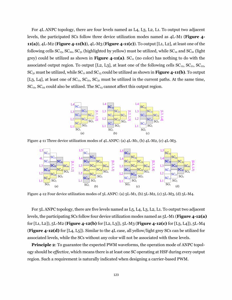
123
For 4L ANPC topology, there are four levels named as L4, L3, L2, L1. To output two adjacent
levels, the participated SCs follow three device utilization modes named as 4L-M1 (Figure 4-
11(a)), 4L-M2 (Figure 4-11(b)), 4L-M3 (Figure 4-11(c)). To output [L1, L2], at least one of the
following cells SC13, SC22, SC31 (highlighted by yellow) must be utilized, while SC12 and SC21 (light
grey) could be utilized as shown in Figure 4-11(a). SC11 (no color) has nothing to do with the
associated output region. To output [L2, L3], at least one of the following cells SC12, SC21, SC22,
SC31 must be utilized, while SC11 and SC13 could be utilized as shown in Figure 4-11(b). To output
[L3, L4], at least one of SC11, SC21, SC31 must be utilized in the current paths. At the same time,
SC12, SC22 could also be utilized. The SC13 cannot affect this output region.
SG1
SG2
SC11
SC12
SC22
SC11
SC13
SC21
SC31
SG3
SG1
SG2
SC11
SC12
SC22
SC11
SC13
SC21
SC31
SG3
SG1
SG2
SC12
SC22
SC13
SC21
SC31
SG3
[L3, L
4]
[L2, L
3]
[L1, L
2]
L1
L2
L3
L4
L1
L2
L3
L4
L1
L2
L3
L4
(a) (b) (c)
SC11
Figure 4-11 Three device utilization modes of 4L ANPC: (a) 4L-M1, (b) 4L-M2, (c) 4L-M3.
SC32
SC23
SC14
SC11
SC12
SC22
SC13
SC21
SC31SC12
SC13
SC22
SG1
SG2
SC11
SC21
SC31
SG3
SC23
SC32
SC41SC41
SG4SC32
SC23
SC14
SC11
SC12
SC22
SC13
SC21
SC31SC12
SC22
SG1
SG2
SC11
SC21
SC31
SG3
SC32
SC41SC41
SG4SC32
SC23
SC14
SC11
SC12
SC22
SC13
SC21
SC31
SC13
SC22
SG1
SG2
SC31
SG3SC14
SC23
SC32
SC41SC41
SG4SC32
SC23
SC14
SC11
SC12
SC22
SC13
SC21
SC31SC12
SC13
SC22
SG1
SG2
SC21
SC31
SG3SC14
SC23
SC32
SC41SC41
SG4
[L3, L
4]
[L2, L
3]
[L1, L
2]
[L4, L
5]
L1
L2
L3
4L
L5
L1
L2
L3
L4
L5
L1
L2
L3
L4
L5
L1
L2
L3
L4
L5
(a) (b) (c) (d) Figure 4-12 Four device utilization modes of 5L ANPC: (a) 5L-M1, (b) 5L-M2, (c) 5L-M3, (d) 5L-M4.
For 5L ANPC topology, there are five levels named as L5, L4, L3, L2, L1. To output two adjacent
levels, the participating SCs follow four device utilization modes named as 5L-M1 (Figure 4-12(a)
for [L1, L2]), 5L-M2 (Figure 4-12(b) for [L2, L3]), 5L-M3 (Figure 4-12(c) for [L3, L4]), 5L-M4
(Figure 4-12(d) for [L4, L5]). Similar to the 4L case, all yellow/light grey SCs can be utilized for
associated levels, while the SCs without any color will not be associated with these levels.
Principle 2: To guarantee the expected PWM waveforms, the operation mode of ANPC topol-
ogy should be effective, which means there is at least one SC operating at HSF during every output
region. Such a requirement is naturally indicated when designing a carrier-based PWM.

124
Although different modulation methods were proposed in the literature, only a small number
of PWM schemes associated with certain operation modes are considered. In [217], a specific
PWM scheme is introduced by applying the virtual-vector concept for a 4L ANPC. In [96], another
operation mode is proposed for a general N-level converter leg, changing the states of N switches
between the transition of two adjacent switching states. Many more operation modes are re-
mained to be derived. This non-exhaustive list will likely lead to unfair conclusions and non-op-
timal overall system operation.
SC14
SC11
SC12
SC13
SC21
5L PWM pattern #1
SC32
SC23
SC22
SC31SC12
SC13
SC22
SG1
SG2
SC11
SC21
SC31
SG3SC14
SC23
SC32
SC41SC41
SG4
SC14
SC11
SC12
SC13
SC21
SC32
SC23
SC22
SC31SC12
SC13
SC22
SG1
SG2
SC11
SC21
SC31
SG3SC14
SC23
SC32
SC41SC41
SG4
SC14
SC11
SC12
SC13
SC21
SC32
SC23
SC22
SC31SC12
SC13
SC22
SG1
SG2
SC11
SC21
SC31
SG3SC14
SC23
SC32
SC41SC41
SG4
SC14
SC11
SC12
SC13
SC21
5L operation mode
SC32
SC23
SC22
SC31SC12
SC13
SC22
SG1
SG2
SC11
SC21
SC31
SG3SC14
SC23
SC32
SC41SC41
SG4
5L PWM pattern #2
5L PWM pattern #3
(b)(a) (c) (d)
L1
L2
L3
L4
L5
L1
L2
L3
L4
L5
L1
L2
L3
L4
L5
L1
L2
L3
L4
L5
Low switching frequency SC
High switching frequency SC
Figure 4-13 (a) 5L operation mode with SG2 operating at HSF, (b) 5L PWM pattern #1, (c) 5L PWM pattern #2, (d) 5L PWM pattern #3.
Moreover, even for the same operation mode, there could be various PWM patterns leading to
various PWM schemes. Take a specific operation mode of 5L ANPC topology as an example. As-
suming that there are three SCs (SC21, SC22, SC23) operating at HSF (see Figure 4-13(a)), the
different utilization of SCs during adjacent levels implies three different PWM patterns as shown
in Figure4-13(b)~(d). The green boxes indicate three possible different 3L modules in the same
operation mode. The 3L modules can be operated with the known 3L PWM pattern shown in
Figure4-8(a). Since each 3L module is for different output regions, for each pattern, the dura-
tion of HSF SCs is different, which implies different schemes.
B. PWM design procedure
To systematically design a complete list of PWM schemes for ANPC converter, one method is to
exhaustively search all the possible operation modes one by one and carry out PWM design pro-
cess for each of them. This can greatly increase the complexity of the PWM design process, par-
ticularly when the number of voltage level is high. To avoid this problem, a systematic PWM de-
sign approach with three simple steps is proposed based on hierarchical decomposition as shown
in Figure 4-14. In step-1, the hierarchical decompositions are derived thoroughly. In step-2, ef-
fective PWM patterns can be implemented for sub-topologies in each hierarchical decomposition
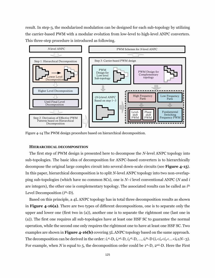
125
result. In step-3, the modularized modulation can be designed for each sub-topology by utilizing
the carrier-based PWM with a modular evolution from low-level to high-level ANPC converters.
This three-step procedure is introduced as following.
Lower Level Decomposition
Higher Level Decomposition
N-level ANPC
Until Final Level Decomposition
Step 1: Hierarchical Decomposition
Step 2: Derivation of Effective PWM Patterns based on Hierarchical
Decomposition
PWM Schemes for N-level ANPC
Step 3: Carrier-based PWM design
PWM Design for Low-level
Sub-topology
PWM Design for Complementary
topology
Fundamental Switching
Frequency PWM
High Frequency Parts
Low Frequency Parts(N-i)-level ANPC
Based on step 1~3
Phase-shift
PWM
Level-shift
PWM
Figure 4-14 The PWM design procedure based on hierarchical decomposition.
HIERARCHICAL DECOMPOSITION
The first step of PWM design is presented here to decompose the N-level ANPC topology into
sub-topologies. The basic idea of decomposition for ANPC-based converters is to hierarchically
decompose the original large complex circuit into several down-scale circuits (see Figure 4-15).
In this paper, hierarchical decomposition is to split N-level ANPC topology into two non-overlap-
ping sub-topologies (which have no common SCs), one is N−i level conventional ANPC (N and i
are integers), the other one is complementary topology. The associated results can be called as ith
Level Decomposition (ith-D).
Based on this principle, a 4L ANPC topology has in total three decomposition results as shown
in Figure 4-16(a). There are two types of different decompositions, one is to separate only the
upper and lower one (first two in (a)), another one is to separate the rightmost one (last one in
(a)). The first one requires all sub-topologies have at least one HSF SC to guarantee the normal
operation, while the second one only requires the rightmost one to have at least one HSF SC. Two
examples are shown in Figure 4-16(b) covering 5L ANPC topology based on the same approach.
The decomposition can be derived in the order: i1st-D, i2nd-D, i3rd-D, …, ikth-D (i1<i2<i3<…<ik≤N−3).
For example, when N is equal to 5, the decomposition order could be 1st-D, 2nd-D. Here the First
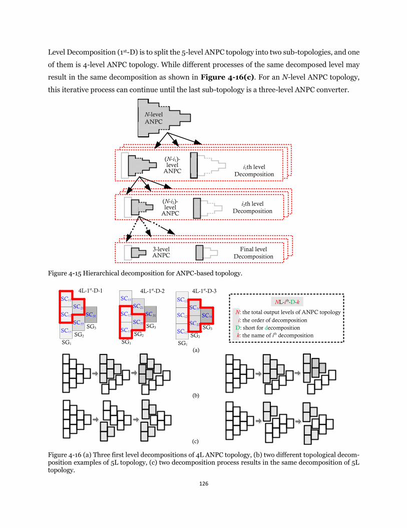
126
Level Decomposition (1st-D) is to split the 5-level ANPC topology into two sub-topologies, and one
of them is 4-level ANPC topology. While different processes of the same decomposed level may
result in the same decomposition as shown in Figure 4-16(c). For an N-level ANPC topology,
this iterative process can continue until the last sub-topology is a three-level ANPC converter.
i1th level Decomposition
Final level Decomposition
N-levelANPC
(N-i1)-level
ANPC
(N-i2)-level
ANPC
3-levelANPC
i2th level Decomposition
Figure 4-15 Hierarchical decomposition for ANPC-based topology.
SC12
SC22
SC13
SC21
SC31SC12
SC13
SC22
SG1
SG2
SC11SC11
SC21
SC31
SG3
4L-1st-D-1
SC12
SC22
SC13
SC21
SC31SC12
SC13
SC22
SG1
SG2
SC11SC11
SC21
SC31
SG3
SC12
SC22
SC13
SC21
SC31SC12
SC13
SC22
SG1
SG2
SC11SC11
SC21
SC31
SG3
4L-1st-D-2 4L-1st-D-3
NL-ith-D-k
N: the total output levels of ANPC topologyi: the order of decomposition
D: short for decompositionk: the name of ith decomposition
(a)
(b)
(c) Figure 4-16 (a) Three first level decompositions of 4L ANPC topology, (b) two different topological decom-position examples of 5L topology, (c) two decomposition process results in the same decomposition of 5L topology.
127
PATTERN DERIVATION
The second step of PWM design is to derive effective PWM patterns of an ANPC topology
through combinations of low-level PWM patterns and hierarchical decomposition results.
To easily obtain all the effective PWM patterns, low-level PWM patterns are utilized as much
as possible. In order to ensure the effectiveness of derived PWM patterns, the operation modes of
sub-topologies should be effective during associated output regions. Take a 4L ANPC as an exam-
ple, there are three 1st-Ds as shown in Figure 4-16. In such a way, a 4-level ANPC topology can
be considered as an iterative representation based on 3L ANPC cells regardless of whatever po-
tential operation modes are applied. For a 3L ANPC topology, there are five PWM patterns that
can guarantee effective operation of whole voltage output ranges with the pulse-width modulated
process as shown in Figure 4-8(a)~(e) [97], [218] (detailed discussion will be provided in the
design example section).
After utilizing all possible PWM patterns of 3L ANPC, various 4L PWM patterns can be derived.
The detailed tables are presented in the Appendix-B. The HSF SCs are indicated as “1”, while
the LSF SCs are noted by “0”. Note that there are patterns have their SCs in the same SG operating
at the same mode (HSF or LSF). They can be referred to as SG-based PWM patterns as shown in
Figure 4-17. From the design modularity point of view, each SG can be considered as a power
electronic building block and is easy to control. Besides, the operation decoupling feature could
facilitate the converter design, enabling proper device selection and optimized thermal manage-
ment. In the next section, PWM design for 4L SG-based PWM patterns will be demonstrated in
detail.
Furthermore, the derivation process of PWM patterns of an arbitrary N-level ANPC can be car-
ried out in a similar way. The ith level decomposition can be derived through one of the possible
iterative processes. Both the N−i level conventional ANPC and the complementary topology
should operate with effective modes to guarantee there is at least one SC operating at HSF during
every output region. Through the proposed process, various PWM patterns can be systematically
obtained. The completeness of this pattern derivations can be proved as shown in Appendix-C.
IMPLEMENTATIONS
As a third step, the PWM schemes are developed for each PWM patterns. For HSF SCs in vari-
ous PWM patterns, pulse-width modulation schemes should be designed to produce the modula-
tion reference. Two types of multicarrier-based PWM can be implemented [85], i.e. level-shift (LS)
PWM, phase-shift (PS) PWM. In [25], PS PWM named doubled frequency PWM can be applied
for 3L ANPC topology to achieve a better loss distribution compared with LS PWM. Based on the
proposed PWM design method, this PWM method can be easily implemented for ANPC topology
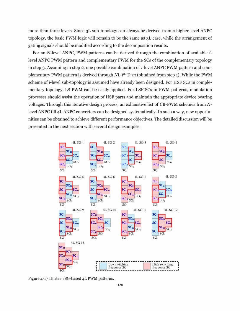
128
more than three levels. Since 3L sub-topology can always be derived from a higher-level ANPC
topology, the basic PWM logic will remain to be the same as 3L case, while the arrangement of
gating signals should be modified according to the decomposition results.
For an N-level ANPC, PWM patterns can be derived through the combination of available i-
level ANPC PWM pattern and complementary PWM for the SCs of the complementary topology
in step 3. Assuming in step 2, one possible combination of i-level ANPC PWM pattern and com-
plementary PWM pattern is derived through NL-ith-D-m (obtained from step 1). While the PWM
scheme of i-level sub-topology is assumed have already been designed. For HSF SCs in comple-
mentary topology, LS PWM can be easily applied. For LSF SCs in PWM patterns, modulation
processes should assist the operation of HSF parts and maintain the appropriate device bearing
voltages. Through this iterative design process, an exhaustive list of CB-PWM schemes from N-
level ANPC till 4L ANPC converters can be designed systematically. In such a way, new opportu-
nities can be obtained to achieve different performance objectives. The detailed discussion will be
presented in the next section with several design examples.
SC12
SC22
SC13
SC21
SC31SC12
SC13
SC22
SG1
SG2
SC11SC11
SC21
SC31
SG3
4L-SG-1
SC12
SC22
SC13
SC21
SC31SC12
SC13
SC22
SG1
SG2
SC11SC11
SC21
SC31
SG3
4L-SG-2
SC12
SC22
SC13
SC21
SC31SC12
SC13
SC22
SG1
SG2
SC11SC11
SC21
SC31
SG3
4L-SG-3
SC12
SC22
SC13
SC21
SC31SC12
SC13
SC22
SG1
SG2
SC11SC11
SC21
SC31
SG3
4L-SG-4
SC12
SC22
SC13
SC21
SC31SC12
SC13
SC22
SG1
SG2
SC11SC11
SC21
SC31
SG3
4L-SG-5
SC12
SC22
SC13
SC21
SC31SC12
SC13
SC22
SG1
SG2
SC11SC11
SC21
SC31
SG3
4L-SG-6
SC12
SC22
SC13
SC21
SC31SC12
SC13
SC22
SG1
SG2
SC11SC11
SC21
SC31
SG3
4L-SG-7
SC12
SC22
SC13
SC21
SC31SC12
SC13
SC22
SG1
SG2
SC11SC11
SC21
SC31
SG3
4L-SG-8
SC12
SC22
SC13
SC21
SC31SC12
SC13
SC22
SG1
SG2
SC11SC11
SC21
SC31
SG3
4L-SG-9
SC12
SC22
SC13
SC21
SC31SC12
SC13
SC22
SG1
SG2
SC11SC11
SC21
SC31
SG3
4L-SG-10
SC12
SC22
SC13
SC21
SC31SC12
SC13
SC22
SG1
SG2
SC11SC11
SC21
SC31
SG3
4L-SG-11
SC12
SC22
SC13
SC21
SC31SC12
SC13
SC22
SG1
SG2
SC11SC11
SC21
SC31
SG3
4L-SG-12
SC12
SC22
SC13
SC21
SC31SC12
SC13
SC22
SG1
SG2
SC11SC11
SC21
SC31
SG3
4L-SG-13
Low switching frequency SC
High switching frequency SC
Figure 4-17 Thirteen SG-based 4L PWM patterns.
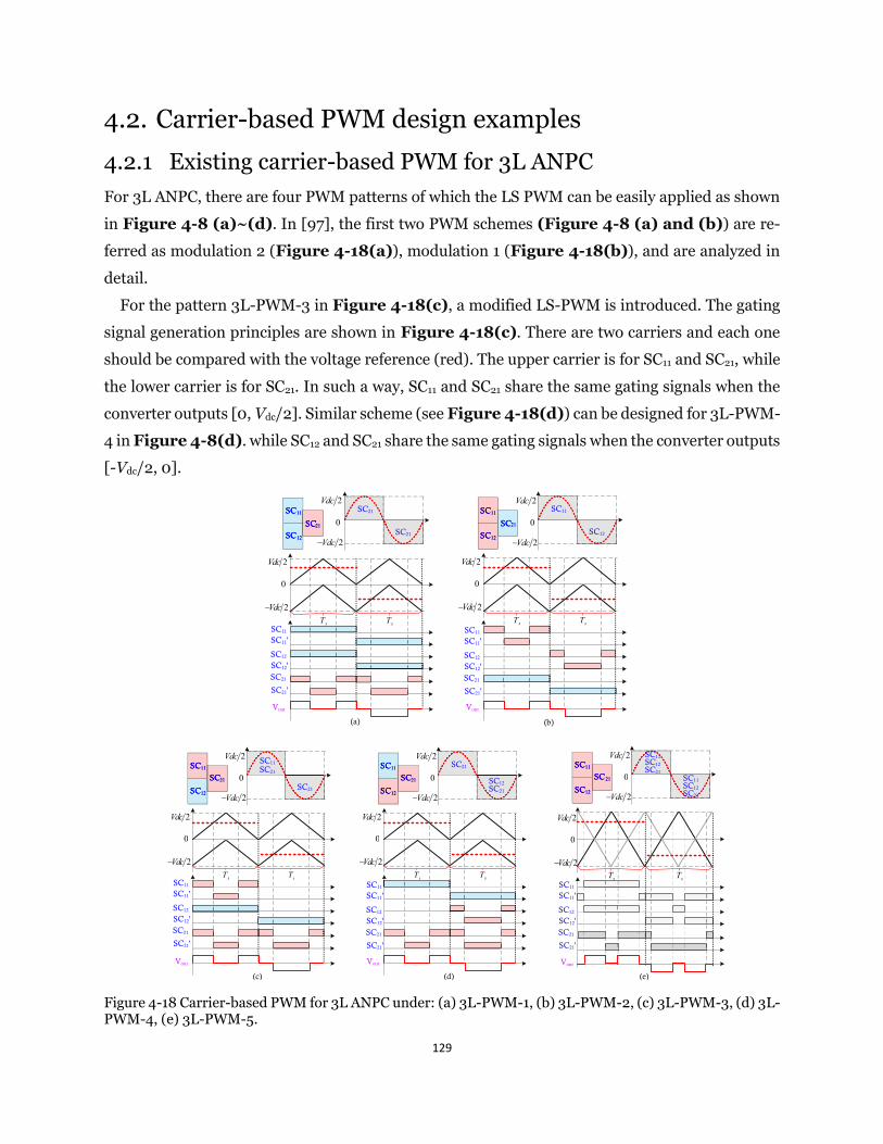
129
4.2. Carrier-based PWM design examples
4.2.1 Existing carrier-based PWM for 3L ANPC
For 3L ANPC, there are four PWM patterns of which the LS PWM can be easily applied as shown
in Figure 4-8 (a)~(d). In [97], the first two PWM schemes (Figure 4-8 (a) and (b)) are re-
ferred as modulation 2 (Figure 4-18(a)), modulation 1 (Figure 4-18(b)), and are analyzed in
detail.
For the pattern 3L-PWM-3 in Figure 4-18(c), a modified LS-PWM is introduced. The gating
signal generation principles are shown in Figure 4-18(c). There are two carriers and each one
should be compared with the voltage reference (red). The upper carrier is for SC11 and SC21, while
the lower carrier is for SC21. In such a way, SC11 and SC21 share the same gating signals when the
converter outputs [0, Vdc/2]. Similar scheme (see Figure 4-18(d)) can be designed for 3L-PWM-
4 in Figure 4-8(d). while SC12 and SC21 share the same gating signals when the converter outputs
[-Vdc/2, 0].
SC11
SC12
SC21
SC12
SC11
SC21
SC21
SC21
2Vdc
0
(a)
sT sT2Vdc−
SC11
SC12
SC21
SC12
SC11
SC21
SC12
SC11
2Vdc
0
Vout
(b)
sT sT2Vdc−
SC11
SC21
SC12'SC12
Vout
SC11'
SC21'
2Vdc
0
2Vdc−
2Vdc
0
2Vdc−
SC11
SC21
SC12'SC12
SC11'
SC21'
SC11
SC12
SC21
SC12
SC11
SC21
SC21
SC11
2Vdc
0
Vout
(c)
sT sT2Vdc−
2Vdc
0
2Vdc−
SC21SC11
SC12
SC21
SC12
SC11
SC21 SC12
SC21
2Vdc
0
Vout
(d)
sT sT2Vdc−
2Vdc
0
2Vdc−SC21
sT sT
Vout
2Vdc
0
2Vdc−
SC11
SC12
SC21
SC12
SC11
SC21
SC12
SC112Vdc
0
2Vdc−
SC21
SC12
SC11
SC21
(e)
SC11
SC21
SC12'SC12
SC11'
SC21'
SC11
SC21
SC12'SC12
SC11'
SC21'
SC11
SC21
SC12'SC12
SC11'
SC21'
Figure 4-18 Carrier-based PWM for 3L ANPC under: (a) 3L-PWM-1, (b) 3L-PWM-2, (c) 3L-PWM-3, (d) 3L-PWM-4, (e) 3L-PWM-5.
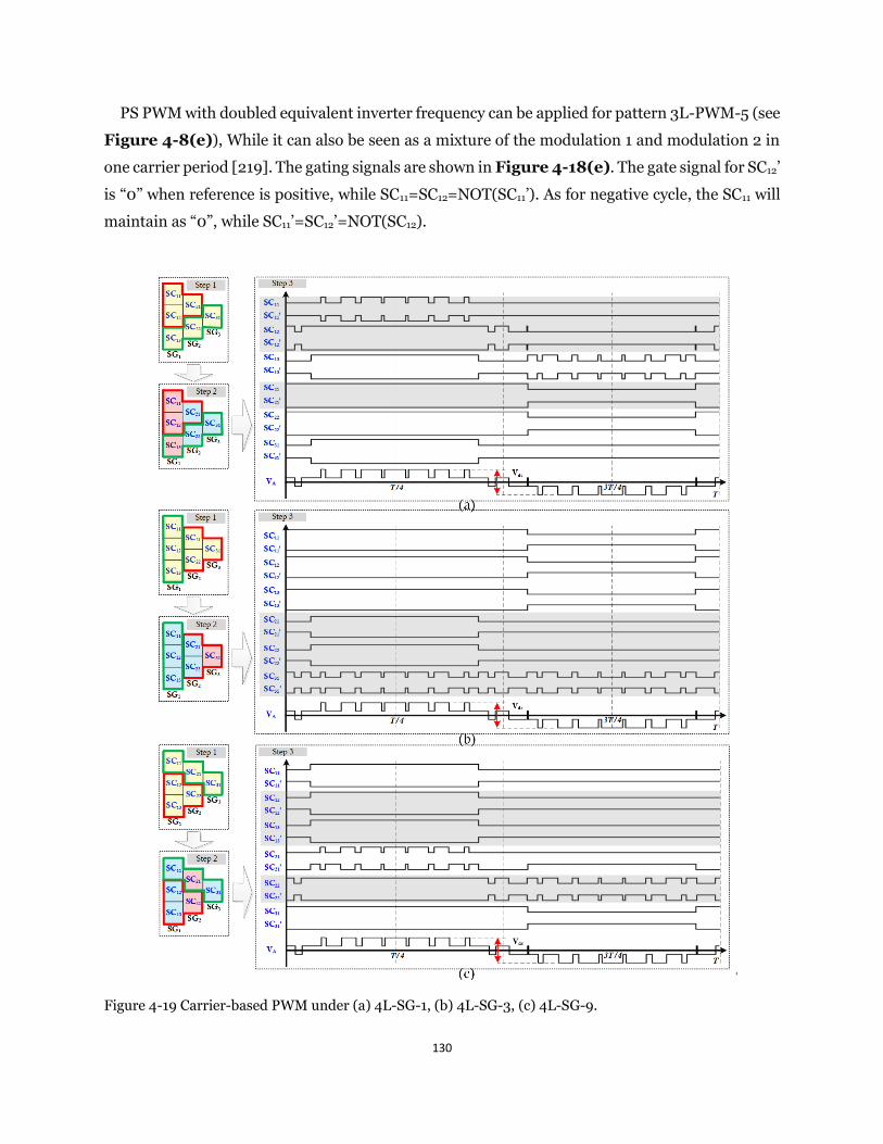
130
PS PWM with doubled equivalent inverter frequency can be applied for pattern 3L-PWM-5 (see
Figure 4-8(e)), While it can also be seen as a mixture of the modulation 1 and modulation 2 in
one carrier period [219]. The gating signals are shown in Figure 4-18(e). The gate signal for SC12’
is “0” when reference is positive, while SC11=SC12=NOT(SC11’). As for negative cycle, the SC11 will
maintain as “0”, while SC11’=SC12’=NOT(SC12).
Figure 4-19 Carrier-based PWM under (a) 4L-SG-1, (b) 4L-SG-3, (c) 4L-SG-9.
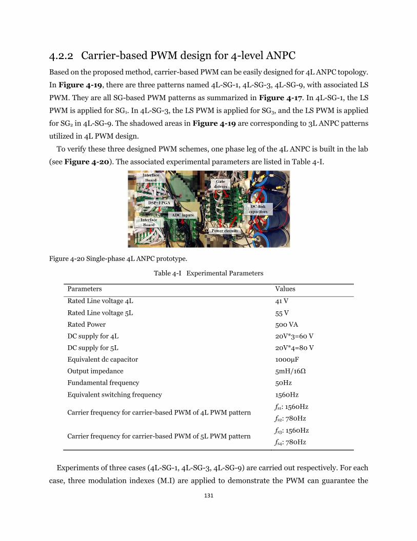
131
4.2.2 Carrier-based PWM design for 4-level ANPC
Based on the proposed method, carrier-based PWM can be easily designed for 4L ANPC topology.
In Figure 4-19, there are three patterns named 4L-SG-1, 4L-SG-3, 4L-SG-9, with associated LS
PWM. They are all SG-based PWM patterns as summarized in Figure 4-17. In 4L-SG-1, the LS
PWM is applied for SG1. In 4L-SG-3, the LS PWM is applied for SG3, and the LS PWM is applied
for SG2 in 4L-SG-9. The shadowed areas in Figure 4-19 are corresponding to 3L ANPC patterns
utilized in 4L PWM design.
To verify these three designed PWM schemes, one phase leg of the 4L ANPC is built in the lab
(see Figure 4-20). The associated experimental parameters are listed in Table 4-I.
Figure 4-20 Single-phase 4L ANPC prototype.
Table 4-I Experimental Parameters
Parameters Values
Rated Line voltage 4L 41 V
Rated Line voltage 5L 55 V
Rated Power 500 VA
DC supply for 4L 20V*3=60 V
DC supply for 5L 20V*4=80 V
Equivalent dc capacitor 1000μF
Output impedance 5mH/16Ω
Fundamental frequency 50Hz
Equivalent switching frequency 1560Hz
Carrier frequency for carrier-based PWM of 4L PWM pattern fs1: 1560Hz
fs2: 780Hz
Carrier frequency for carrier-based PWM of 5L PWM pattern fs3: 1560Hz
fs4: 780Hz
Experiments of three cases (4L-SG-1, 4L-SG-3, 4L-SG-9) are carried out respectively. For each
case, three modulation indexes (M.I) are applied to demonstrate the PWM can guarantee the
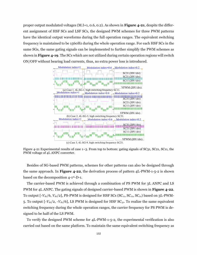
132
proper output modulated voltages (M.I=1, 0.6, 0.2). As shown in Figure 4-21, despite the differ-
ent assignment of HSF SCs and LSF SCs, the designed PWM schemes for three PWM patterns
have the identical output waveforms during the full operation ranges. The equivalent switching
frequency is maintained to be 1560Hz during the whole operation range. For each HSF SCs in the
same SGs, the same gating signals can be implemented to further simplify the PWM schemes as
shown in Figure 4-19. The SCs which are not utilized during certain operation regions will switch
ON/OFF without bearing load currents, thus, no extra power loss is introduced.
Modulation index=1 Modulation index=0.6 Modulation index=0.2
SC11 (20V/div)
SC21 (20V/div)SC31 (20V/div)
VPWM (20V/div)(a) Case 1, 4L-SG-1, high switching frequency SC11.
Modulation index=1 Modulation index=0.6 Modulation index=0.2
SC11 (20V/div)SC21 (20V/div)
SC31 (20V/div)
VPWM (20V/div)(b) Case 2, 4L-SG-3, high switching frequency SC31.
Modulation index=1 Modulation index=0.6 Modulation index=0.2
SC11 (20V/div)SC21 (20V/div)
SC31 (20V/div)
VPWM (20V/div)(c) Case 3, 4L-SG-9, high switching frequency SC21.
Figure 4-21 Experimental results of case 1~3. From top to bottom: gating signals of SC31, SC21, SC11, the PWM voltage of 4L ANPC converter.
Besides of SG-based PWM patterns, schemes for other patterns can also be designed through
the same approach. In Figure 4-22, the derivation process of pattern 4L-PWM-1-5-2 is shown
based on the decomposition 4-1st-D-1.
The carrier-based PWM is achieved through a combination of PS PWM for 3L ANPC and LS
PWM for 4L ANPC. The gating signals of designed carrier-based PWM is shown in Figure 4-22.
To output [-Vdc/6, Vdc/2], PS-PWM is designed for HSF SCs (SC11, SC12, SC21) based on 3L-PWM-
5. To output [-Vdc/2, -Vdc/6], LS PWM is designed for HSF SC31. To realize the same equivalent
switching frequency during the whole operation ranges, the carrier frequency for PS PWM is de-
signed to be half of the LS PWM.
To verify the designed PWM scheme for 4L-PWM-1-5-2, the experimental verification is also
carried out based on the same platform. To maintain the same equivalent switching frequency as
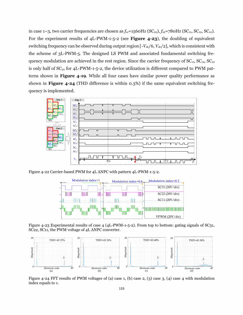
133
in case 1~3, two carrier frequencies are chosen as fs1=1560Hz (SC22), fs2=780Hz (SC11, SC12, SC21).
For the experiment results of 4L-PWM-1-5-2 (see Figure 4-23), the doubling of equivalent
switching frequency can be observed during output region [-Vdc/6, Vdc/2], which is consistent with
the scheme of 3L-PWM-5. The designed LS PWM and associated fundamental switching fre-
quency modulation are achieved in the rest region. Since the carrier frequency of SC11, SC12, SC21
is only half of SC22 for 4L-PWM-1-5-2, the device utilization is different compared to PWM pat-
terns shown in Figure 4-19. While all four cases have similar power quality performance as
shown in Figure 4-24 (THD difference is within 0.3%) if the same equivalent switching fre-
quency is implemented.
Figure 4-22 Carrier-based PWM for 4L ANPC with pattern 4L-PWM-1-5-2.
Modulation index=1 Modulation index=0.6 Modulation index=0.2
SC11 (20V/div)
SC22 (20V/div)
SC31 (20V/div)
VPWM (20V/div)
Figure 4-23 Experimental results of case 4 (4L-PWM-1-5-2). From top to bottom: gating signals of SC31, SC22, SC11, the PWM voltage of 4L ANPC converter.
0
30
40Harmonic order
THD=43.55%
fs1
0
30
40Harmonic order
THD=43.54%
fs1
0
30
40Harmonic order
Ma
gnit
ud
e
THD=43.60%
fs1Ma
gnit
ud
e
Ma
gnit
ud
e
0
30
40Harmonic order
THD=43.36%
fs1
Ma
gnit
ud
e
(a) (b) (c) (d)
Figure 4-24 FFT results of PWM voltages of (a) case 1, (b) case 2, (3) case 3, (4) case 4 with modulation index equals to 1.
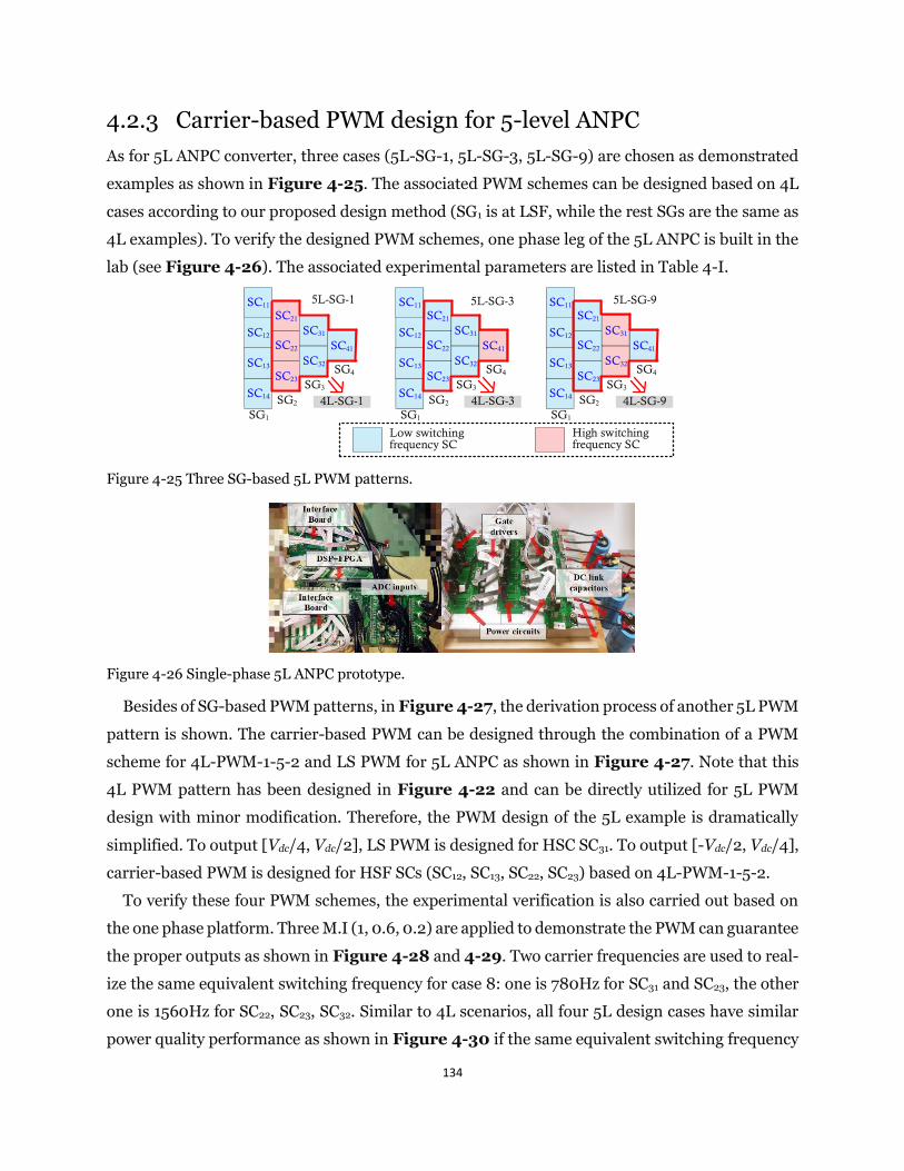
134
4.2.3 Carrier-based PWM design for 5-level ANPC
As for 5L ANPC converter, three cases (5L-SG-1, 5L-SG-3, 5L-SG-9) are chosen as demonstrated
examples as shown in Figure 4-25. The associated PWM schemes can be designed based on 4L
cases according to our proposed design method (SG1 is at LSF, while the rest SGs are the same as
4L examples). To verify the designed PWM schemes, one phase leg of the 5L ANPC is built in the
lab (see Figure 4-26). The associated experimental parameters are listed in Table 4-I.
SC22
SC32
SC23
SC31
SC41
SG1
SG2
SC21
SG3
5L-SG-1
Low switching frequency SC
High switching frequency SC
SC12
SC11
SC14
SC13 SG4
SC22
SC32
SC23
SC31
SC41
SG1
SG2
SC21
SG3
5L-SG-9
SC12
SC11
SC14
SC13 SG4
SC22
SC32
SC23
SC31
SC41
SG1
SG2
SC21
SG3
5L-SG-3
SC12
SC11
SC14
SC13 SG4
4L-SG-1 4L-SG-94L-SG-3
Figure 4-25 Three SG-based 5L PWM patterns.
Figure 4-26 Single-phase 5L ANPC prototype.
Besides of SG-based PWM patterns, in Figure 4-27, the derivation process of another 5L PWM
pattern is shown. The carrier-based PWM can be designed through the combination of a PWM
scheme for 4L-PWM-1-5-2 and LS PWM for 5L ANPC as shown in Figure 4-27. Note that this
4L PWM pattern has been designed in Figure 4-22 and can be directly utilized for 5L PWM
design with minor modification. Therefore, the PWM design of the 5L example is dramatically
simplified. To output [Vdc/4, Vdc/2], LS PWM is designed for HSC SC31. To output [-Vdc/2, Vdc/4],
carrier-based PWM is designed for HSF SCs (SC12, SC13, SC22, SC23) based on 4L-PWM-1-5-2.
To verify these four PWM schemes, the experimental verification is also carried out based on
the one phase platform. Three M.I (1, 0.6, 0.2) are applied to demonstrate the PWM can guarantee
the proper outputs as shown in Figure 4-28 and 4-29. Two carrier frequencies are used to real-
ize the same equivalent switching frequency for case 8: one is 780Hz for SC31 and SC23, the other
one is 1560Hz for SC22, SC23, SC32. Similar to 4L scenarios, all four 5L design cases have similar
power quality performance as shown in Figure 4-30 if the same equivalent switching frequency
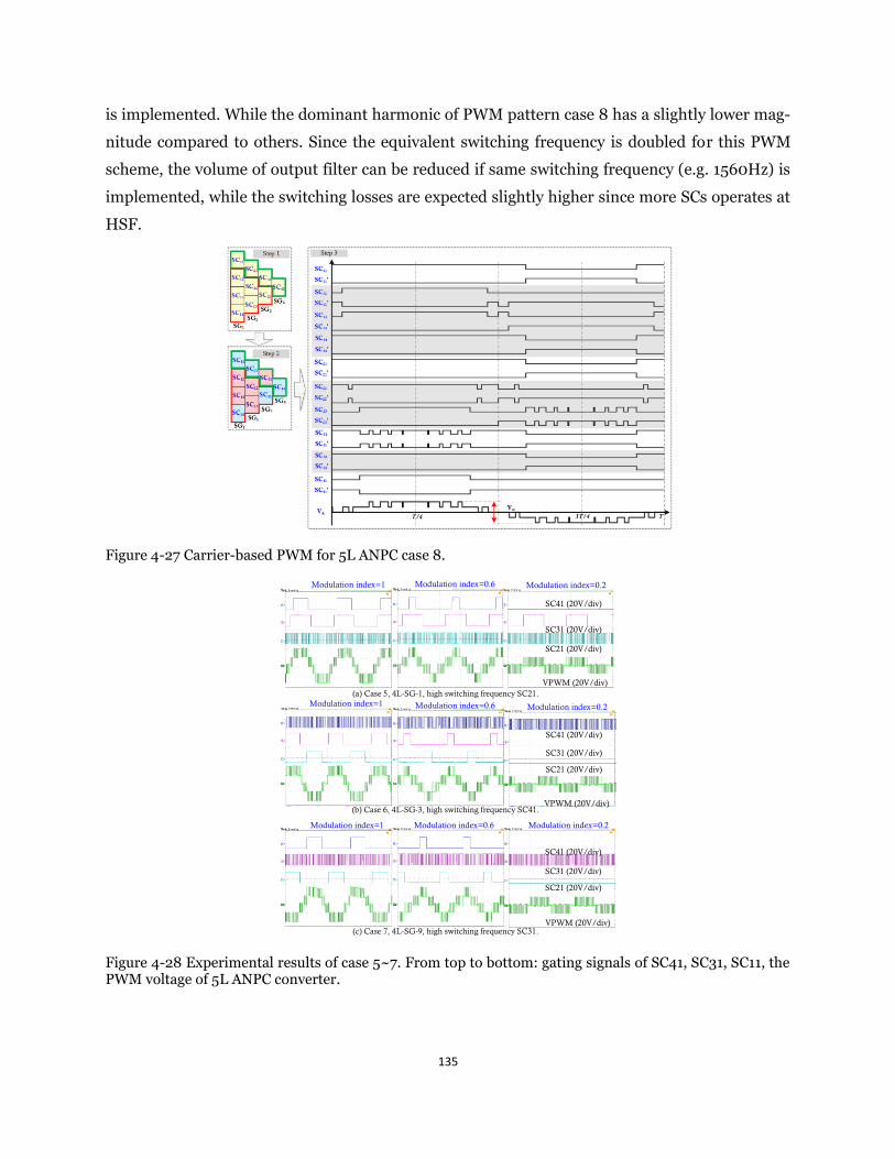
135
is implemented. While the dominant harmonic of PWM pattern case 8 has a slightly lower mag-
nitude compared to others. Since the equivalent switching frequency is doubled for this PWM
scheme, the volume of output filter can be reduced if same switching frequency (e.g. 1560Hz) is
implemented, while the switching losses are expected slightly higher since more SCs operates at
HSF.
Figure 4-27 Carrier-based PWM for 5L ANPC case 8.
Modulation index=1 Modulation index=0.6 Modulation index=0.2
SC21 (20V/div)
SC31 (20V/div)
SC41 (20V/div)
VPWM (20V/div)(a) Case 5, 4L-SG-1, high switching frequency SC21.
Modulation index=1 Modulation index=0.6 Modulation index=0.2
SC21 (20V/div)
SC31 (20V/div)
SC41 (20V/div)
VPWM (20V/div)(b) Case 6, 4L-SG-3, high switching frequency SC41.
Modulation index=1 Modulation index=0.6 Modulation index=0.2
SC21 (20V/div)
SC31 (20V/div)
SC41 (20V/div)
VPWM (20V/div)(c) Case 7, 4L-SG-9, high switching frequency SC31.
Figure 4-28 Experimental results of case 5~7. From top to bottom: gating signals of SC41, SC31, SC11, the PWM voltage of 5L ANPC converter.
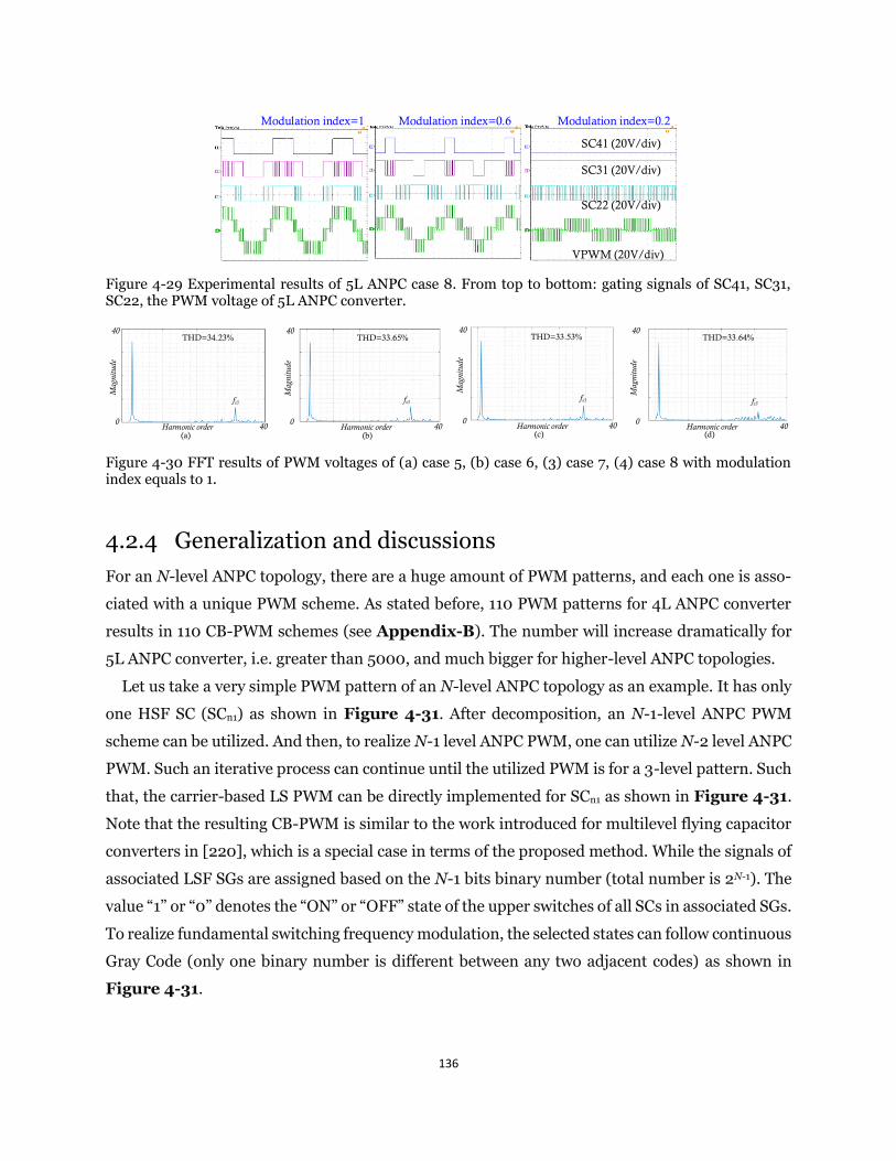
136
Modulation index=1 Modulation index=0.6 Modulation index=0.2
SC22 (20V/div)
SC31 (20V/div)
SC41 (20V/div)
VPWM (20V/div)
Figure 4-29 Experimental results of 5L ANPC case 8. From top to bottom: gating signals of SC41, SC31, SC22, the PWM voltage of 5L ANPC converter.
0
40
40Harmonic order
THD=34.23%
fs3
0
40
40Harmonic order
THD=33.65%
fs3
0
40
40Harmonic order
Ma
gnit
ud
e
THD=33.53%
fs3
Ma
gnit
ud
e
Ma
gnit
ud
e
0
40
40Harmonic order
THD=33.64%
fs3
Ma
gnit
ud
e
(a) (b) (c) (d)
Figure 4-30 FFT results of PWM voltages of (a) case 5, (b) case 6, (3) case 7, (4) case 8 with modulation index equals to 1.
4.2.4 Generalization and discussions
For an N-level ANPC topology, there are a huge amount of PWM patterns, and each one is asso-
ciated with a unique PWM scheme. As stated before, 110 PWM patterns for 4L ANPC converter
results in 110 CB-PWM schemes (see Appendix-B). The number will increase dramatically for
5L ANPC converter, i.e. greater than 5000, and much bigger for higher-level ANPC topologies.
Let us take a very simple PWM pattern of an N-level ANPC topology as an example. It has only
one HSF SC (SCn1) as shown in Figure 4-31. After decomposition, an N-1-level ANPC PWM
scheme can be utilized. And then, to realize N-1 level ANPC PWM, one can utilize N-2 level ANPC
PWM. Such an iterative process can continue until the utilized PWM is for a 3-level pattern. Such
that, the carrier-based LS PWM can be directly implemented for SCn1 as shown in Figure 4-31.
Note that the resulting CB-PWM is similar to the work introduced for multilevel flying capacitor
converters in [220], which is a special case in terms of the proposed method. While the signals of
associated LSF SGs are assigned based on the N-1 bits binary number (total number is 2N-1). The
value “1” or “0” denotes the “ON” or “OFF” state of the upper switches of all SCs in associated SGs.
To realize fundamental switching frequency modulation, the selected states can follow continuous
Gray Code (only one binary number is different between any two adjacent codes) as shown in
Figure 4-31.
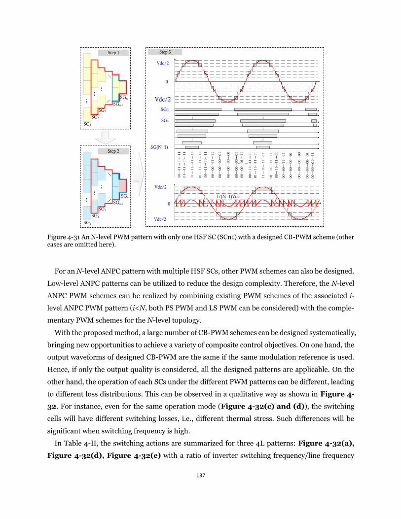
137
Step 3
Step 2
Step 1
SG1
SG2
SG3
SGn-1
SGn
SG1
SG2
SG3
SGn-1
SGn
Vdc/2
0
Vdc/2
SG1
SGi
SG(N 1)
11
11
11
11
11
11
11
10
11
11
11
00
11
11
00
00
10
00
00
00
00
00
00
00
11
11
11
10
11
11
11
00
10
00
00
00
11
10
00
00
11
11
11
11
11
11
11
10
11
11
11
00
11
11
00
00
10
00
00
00
00
00
00
00
11
11
11
10
11
11
11
00
10
00
00
00
11
10
00
00
Vdc/2
0
Vdc/2
1/(N 1)Vdc
Figure 4-31 An N-level PWM pattern with only one HSF SC (SCn1) with a designed CB-PWM scheme (other cases are omitted here).
For an N-level ANPC pattern with multiple HSF SCs, other PWM schemes can also be designed.
Low-level ANPC patterns can be utilized to reduce the design complexity. Therefore, the N-level
ANPC PWM schemes can be realized by combining existing PWM schemes of the associated i-
level ANPC PWM pattern (i<N, both PS PWM and LS PWM can be considered) with the comple-
mentary PWM schemes for the N-level topology.
With the proposed method, a large number of CB-PWM schemes can be designed systematically,
bringing new opportunities to achieve a variety of composite control objectives. On one hand, the
output waveforms of designed CB-PWM are the same if the same modulation reference is used.
Hence, if only the output quality is considered, all the designed patterns are applicable. On the
other hand, the operation of each SCs under the different PWM patterns can be different, leading
to different loss distributions. This can be observed in a qualitative way as shown in Figure 4-
32. For instance, even for the same operation mode (Figure 4-32(c) and (d)), the switching
cells will have different switching losses, i.e., different thermal stress. Such differences will be
significant when switching frequency is high.
In Table 4-II, the switching actions are summarized for three 4L patterns: Figure 4-32(a),
Figure 4-32(d), Figure 4-32(e) with a ratio of inverter switching frequency/line frequency
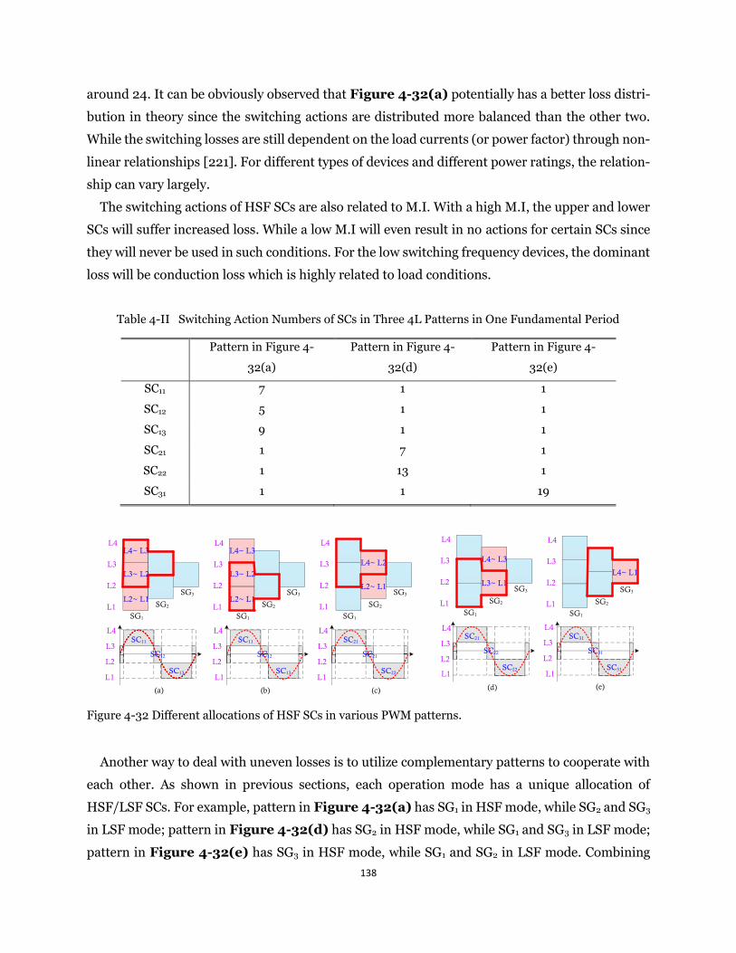
138
around 24. It can be obviously observed that Figure 4-32(a) potentially has a better loss distri-
bution in theory since the switching actions are distributed more balanced than the other two.
While the switching losses are still dependent on the load currents (or power factor) through non-
linear relationships [221]. For different types of devices and different power ratings, the relation-
ship can vary largely.
The switching actions of HSF SCs are also related to M.I. With a high M.I, the upper and lower
SCs will suffer increased loss. While a low M.I will even result in no actions for certain SCs since
they will never be used in such conditions. For the low switching frequency devices, the dominant
loss will be conduction loss which is highly related to load conditions.
Table 4-II Switching Action Numbers of SCs in Three 4L Patterns in One Fundamental Period
Pattern in Figure 4-
32(a)
Pattern in Figure 4-
32(d)
Pattern in Figure 4-
32(e)
SC11 7 1 1
SC12 5 1 1
SC13 9 1 1
SC21 1 7 1
SC22 1 13 1
SC31 1 1 19
(a)
L1
L2
L3
L4
SG1
SG2
SG3
SG1
SG2
SG3
SG1
SG2
SG3
L4~ L3
L3~ L2
L2~ L1
L4~ L2
L1
L2
L3
L4
L1
L2
L3
L4
L2~ L1
L4~ L1
(d) (e)(b)
L1
L2
L3
L4
SG1
SG2
SG3
L4~ L3
L3~ L2
L2~ L1
SG1
SG2
SG3
L4~ L3
L1
L2
L3
L4
L3~ L1
(c)
SC11
L1
L2
L3
L4
SC12
SC13
SC11
L1
L2
L3
L4
SC12
SC13
SC21
L1
L2
L3
L4
SC21
SC22
SC21
L1
L2
L3
L4
SC22
SC22
SC31
L1
L2
L3
L4
SC31
SC31
Figure 4-32 Different allocations of HSF SCs in various PWM patterns.
Another way to deal with uneven losses is to utilize complementary patterns to cooperate with
each other. As shown in previous sections, each operation mode has a unique allocation of
HSF/LSF SCs. For example, pattern in Figure 4-32(a) has SG1 in HSF mode, while SG2 and SG3
in LSF mode; pattern in Figure 4-32(d) has SG2 in HSF mode, while SG1 and SG3 in LSF mode;
pattern in Figure 4-32(e) has SG3 in HSF mode, while SG1 and SG2 in LSF mode. Combining
139
those three patterns and rotate them during a long time constant, one can equivalently operate
the converter with all SCs in HSF mode. In such a way, all the SCs can be operated with a similar
number of switching actions and share the loss more evenly. Moreover, such complementary pat-
terns can be easily found in the derived complete list of patterns and have many freedoms of de-
grees to implement. In Appendix-B, the patterns with logically opposite SC modes are comple-
mentary with each other, such as 4L-PWM-1-1-1 denoted as 001100 is complementary with 4L-
PWM-1-2-5 denoted as 110011. While the overall performance relies on how optimally we utilize
the various patterns to achieve the control goals.
In summary, to overcome the increasing PWM design complexity of multilevel converter with
a high number of output levels and possible PWM patterns, e.g. ANPC converter, a universal car-
rier-based PWM design method based on isomorphic theory is proposed. Based on the hierar-
chical decomposition process, the complete sets of PWM patterns can be derived. Even with a
high number of PWM patterns, the design process is dramatically simplified by utilizing low-level
sub-topologies (i.e. isomorphisms between two converters). Several designed PWM schemes un-
der different operation modes are verified through experiments and demonstrate how the same
approach can also be generalized for a high-level ANPC topology (e.g. 3L to 4L, 4L to 5L).
With the help of this simplified and unified method, a complete design of an exhaustive list of
CB-PWM schemes of ANPC-based topology can be achieved. Such a complete list of PWM
schemes provide the opportunity for optimal selection and utilization of PWM schemes in a more
comprehensive way.
4.3. Phase shift PWM design for ANPC-based converter
For multilevel converters, especially when output level number is higher than three, carrier-based
PWM schemes, i.e., LS and PS PWM, are much easier to implement than SVM methods. While
conventional LS PWM tends to cause unequal loss distribution [219]. An alternative method is to
develop PS PWM which has been successfully applied for state-of-art topologies to achieve higher
equivalent switching frequency (ESF), better device utilization, and evenly loss distribution. Re-
cently, a hybrid PWM scheme has been applied in hybrid-clamped converters [100], [101], [222].
The converter is controlled by a 3L PS PWM for FC legs and low switching frequency modulation
for a 3L ANPC converter. However, it cannot be applied for ANPC converter since no FC legs exist
in ANPC converters. For the conventional PS PWM schemes of cascaded H-bridge or modular
multilevel converter, they utilize the inherent modular structures and generate the phase-shifted
PWM signals for each submodule [99]. Unfortunately, due to the different topology operation
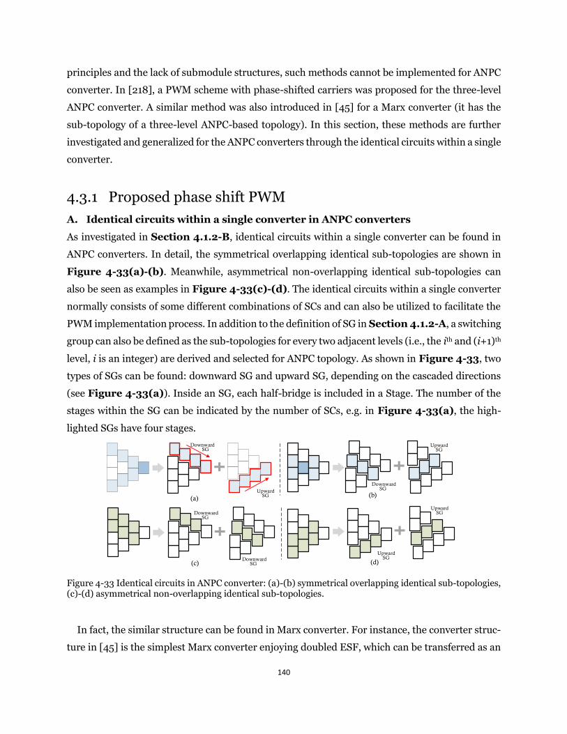
140
principles and the lack of submodule structures, such methods cannot be implemented for ANPC
converter. In [218], a PWM scheme with phase-shifted carriers was proposed for the three-level
ANPC converter. A similar method was also introduced in [45] for a Marx converter (it has the
sub-topology of a three-level ANPC-based topology). In this section, these methods are further
investigated and generalized for the ANPC converters through the identical circuits within a single
converter.
4.3.1 Proposed phase shift PWM
A. Identical circuits within a single converter in ANPC converters
As investigated in Section 4.1.2-B, identical circuits within a single converter can be found in
ANPC converters. In detail, the symmetrical overlapping identical sub-topologies are shown in
Figure 4-33(a)-(b). Meanwhile, asymmetrical non-overlapping identical sub-topologies can
also be seen as examples in Figure 4-33(c)-(d). The identical circuits within a single converter
normally consists of some different combinations of SCs and can also be utilized to facilitate the
PWM implementation process. In addition to the definition of SG in Section 4.1.2-A, a switching
group can also be defined as the sub-topologies for every two adjacent levels (i.e., the ith and (i+1)th
level, i is an integer) are derived and selected for ANPC topology. As shown in Figure 4-33, two
types of SGs can be found: downward SG and upward SG, depending on the cascaded directions
(see Figure 4-33(a)). Inside an SG, each half-bridge is included in a Stage. The number of the
stages within the SG can be indicated by the number of SCs, e.g. in Figure 4-33(a), the high-
lighted SGs have four stages.
(a) (b)
(c) (d)
Downward SG
UpwardSG
Downward SG
Downward SG
UpwardSG
Downward SG
UpwardSG
UpwardSG
Figure 4-33 Identical circuits in ANPC converter: (a)-(b) symmetrical overlapping identical sub-topologies, (c)-(d) asymmetrical non-overlapping identical sub-topologies.
In fact, the similar structure can be found in Marx converter. For instance, the converter struc-
ture in [45] is the simplest Marx converter enjoying doubled ESF, which can be transferred as an
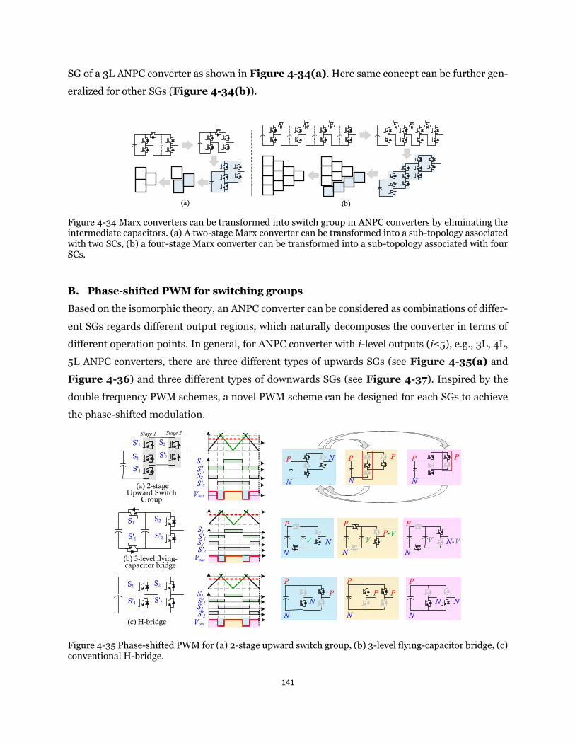
141
SG of a 3L ANPC converter as shown in Figure 4-34(a). Here same concept can be further gen-
eralized for other SGs (Figure 4-34(b)).
(a) (b) Figure 4-34 Marx converters can be transformed into switch group in ANPC converters by eliminating the intermediate capacitors. (a) A two-stage Marx converter can be transformed into a sub-topology associated with two SCs, (b) a four-stage Marx converter can be transformed into a sub-topology associated with four SCs.
B. Phase-shifted PWM for switching groups
Based on the isomorphic theory, an ANPC converter can be considered as combinations of differ-
ent SGs regards different output regions, which naturally decomposes the converter in terms of
different operation points. In general, for ANPC converter with i-level outputs (i≤5), e.g., 3L, 4L,
5L ANPC converters, there are three different types of upwards SGs (see Figure 4-35(a) and
Figure 4-36) and three different types of downwards SGs (see Figure 4-37). Inspired by the
double frequency PWM schemes, a novel PWM scheme can be designed for each SGs to achieve
the phase-shifted modulation.
Vout
S'1
S1
S'1
S'2
S2
S'1S1
S'2S2
(a) 2-stage Upward Switch
Group
P
N
PP
N
N P
N
P
Vout
S'1
S1
S'2
S2
S'1S1
S'2S2
(c) H-bridge
P
N
P
N
P
N
N NP
NP
Vout
S'1
S1
S'2
S2
S'1S1
S'2S2
(b) 3-level flying-capacitor bridge
P
N
V
P
N
V
P
N
VNP V-
N V-
P
Stage 1 Stage 2
Figure 4-35 Phase-shifted PWM for (a) 2-stage upward switch group, (b) 3-level flying-capacitor bridge, (c) conventional H-bridge.
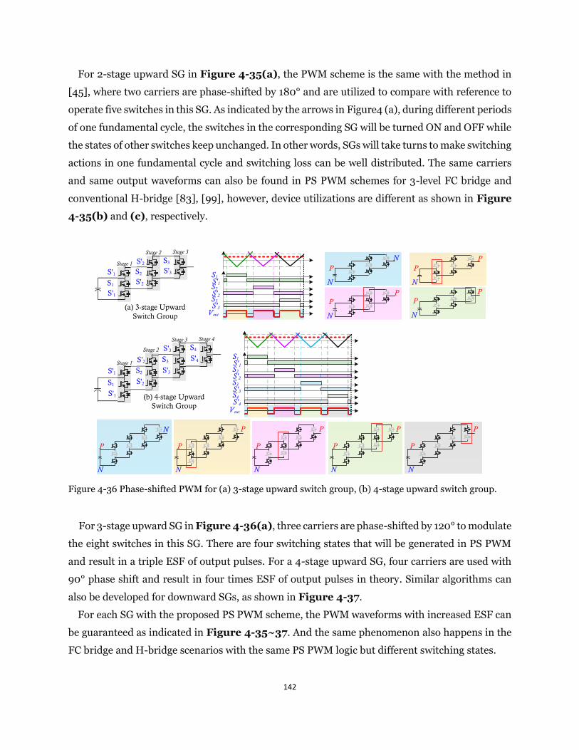
142
For 2-stage upward SG in Figure 4-35(a), the PWM scheme is the same with the method in
[45], where two carriers are phase-shifted by 180° and are utilized to compare with reference to
operate five switches in this SG. As indicated by the arrows in Figure4 (a), during different periods
of one fundamental cycle, the switches in the corresponding SG will be turned ON and OFF while
the states of other switches keep unchanged. In other words, SGs will take turns to make switching
actions in one fundamental cycle and switching loss can be well distributed. The same carriers
and same output waveforms can also be found in PS PWM schemes for 3-level FC bridge and
conventional H-bridge [83], [99], however, device utilizations are different as shown in Figure
4-35(b) and (c), respectively.
Vout
S'1S1
S'3S3
S'1
S1
S'1S'2
S2
S'2S'3
S3
S'2S2
Vout
S'1S1
S'3S3
S'2S2
S'4S4
S'1
S1
S'1S'2
S2
S'2S'3
S3
S'3S'4
S4
(a) 3-stage Upward Switch Group
(b) 4-stage Upward Switch Group
P
N
NP
N
P
P
N
PP
N
P
P
N
N
P
N
P
N
P
N
P
N
P P P P
Stage 2 Stage 3
Stage 1
Stage 3 Stage 4
Stage 2
Stage 1
Figure 4-36 Phase-shifted PWM for (a) 3-stage upward switch group, (b) 4-stage upward switch group.
For 3-stage upward SG in Figure 4-36(a), three carriers are phase-shifted by 120° to modulate
the eight switches in this SG. There are four switching states that will be generated in PS PWM
and result in a triple ESF of output pulses. For a 4-stage upward SG, four carriers are used with
90° phase shift and result in four times ESF of output pulses in theory. Similar algorithms can
also be developed for downward SGs, as shown in Figure 4-37.
For each SG with the proposed PS PWM scheme, the PWM waveforms with increased ESF can
be guaranteed as indicated in Figure 4-35~37. And the same phenomenon also happens in the
FC bridge and H-bridge scenarios with the same PS PWM logic but different switching states.
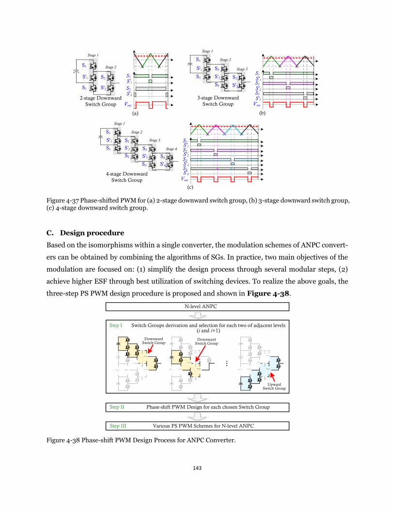
143
Vout
S'1S1
S'2S2
Vout
S'1S1
S'3S3
S'2S2
Vout
S'1S1
S'3S3
S'2S2
S'4S4
(a) (b)
(c)
S1
S'1
S1
S'2
S2 S1
S'1
S1
S'2
S2
S2 S'3
S3
S1
S'1
S1
S'2
S2
S2 S'3
S3
S3 S'4
S4
2-stage Downward Switch Group
3-stage Downward Switch Group
4-stage Downward Switch Group
3
Stage 2
Stage 3
Stage 1Stage 1
Stage 2
4
Stage 3
Stage 4
Stage 2
Stage 1
Figure 4-37 Phase-shifted PWM for (a) 2-stage downward switch group, (b) 3-stage downward switch group, (c) 4-stage downward switch group.
C. Design procedure
Based on the isomorphisms within a single converter, the modulation schemes of ANPC convert-
ers can be obtained by combining the algorithms of SGs. In practice, two main objectives of the
modulation are focused on: (1) simplify the design process through several modular steps, (2)
achieve higher ESF through best utilization of switching devices. To realize the above goals, the
three-step PS PWM design procedure is proposed and shown in Figure 4-38.
N-level ANPC
Switch Groups derivation and selection for each two of adjacent levels (i and i+1)
Phase-shift PWM Design for each chosen Switch Group
Various PS PWM Schemes for N-level ANPC
Step I
Step II
Step III
Downward Switch Group
Downward Switch Group
Upward Switch Group
Figure 4-38 Phase-shift PWM Design Process for ANPC Converter.
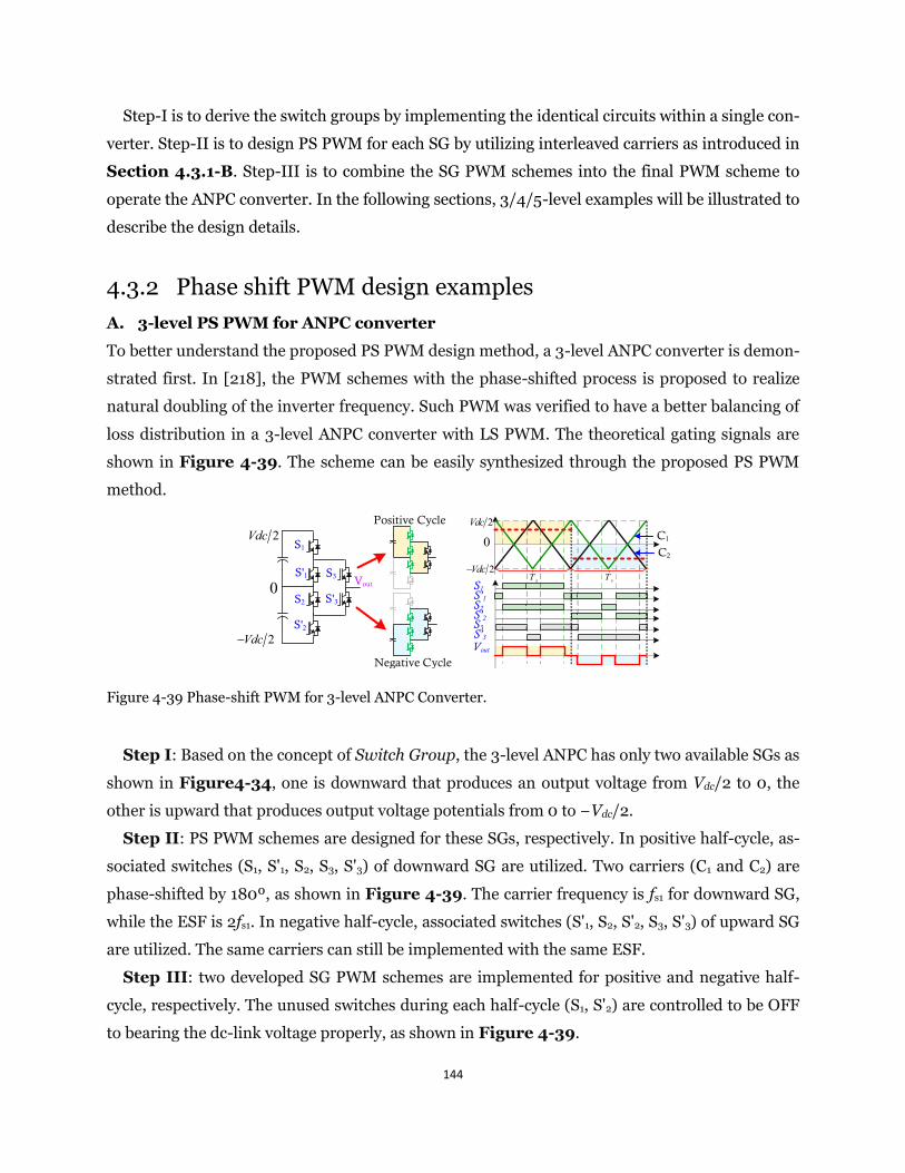
144
Step-I is to derive the switch groups by implementing the identical circuits within a single con-
verter. Step-II is to design PS PWM for each SG by utilizing interleaved carriers as introduced in
Section 4.3.1-B. Step-III is to combine the SG PWM schemes into the final PWM scheme to
operate the ANPC converter. In the following sections, 3/4/5-level examples will be illustrated to
describe the design details.
4.3.2 Phase shift PWM design examples
A. 3-level PS PWM for ANPC converter
To better understand the proposed PS PWM design method, a 3-level ANPC converter is demon-
strated first. In [218], the PWM schemes with the phase-shifted process is proposed to realize
natural doubling of the inverter frequency. Such PWM was verified to have a better balancing of
loss distribution in a 3-level ANPC converter with LS PWM. The theoretical gating signals are
shown in Figure 4-39. The scheme can be easily synthesized through the proposed PS PWM
method.
S1
Vout
sT sT
S'1S2S'2S3S'3
S'1
S1
S'3
S3
S'2
S2
Vout
2Vdc
0
2Vdc−
2Vdc−
02Vdc
C1
C2
Positive Cycle
Negative Cycle Figure 4-39 Phase-shift PWM for 3-level ANPC Converter.
Step I: Based on the concept of Switch Group, the 3-level ANPC has only two available SGs as
shown in Figure4-34, one is downward that produces an output voltage from Vdc/2 to 0, the
other is upward that produces output voltage potentials from 0 to −Vdc/2.
Step II: PS PWM schemes are designed for these SGs, respectively. In positive half-cycle, as-
sociated switches (S1, S'1, S2, S3, S'3) of downward SG are utilized. Two carriers (C1 and C2) are
phase-shifted by 180º, as shown in Figure 4-39. The carrier frequency is fs1 for downward SG,
while the ESF is 2fs1. In negative half-cycle, associated switches (S'1, S2, S'2, S3, S'3) of upward SG
are utilized. The same carriers can still be implemented with the same ESF.
Step III: two developed SG PWM schemes are implemented for positive and negative half-
cycle, respectively. The unused switches during each half-cycle (S1, S'2) are controlled to be OFF
to bearing the dc-link voltage properly, as shown in Figure 4-39.
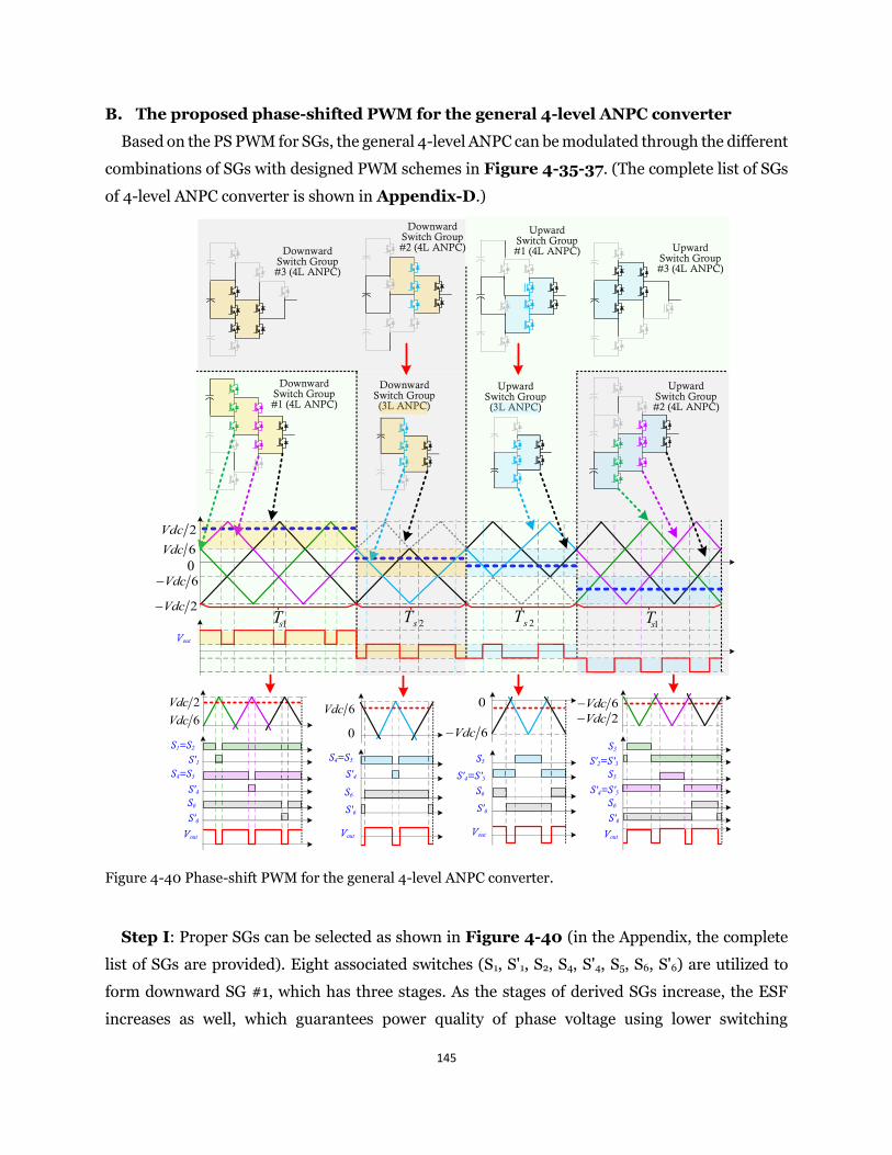
145
B. The proposed phase-shifted PWM for the general 4-level ANPC converter
Based on the PS PWM for SGs, the general 4-level ANPC can be modulated through the different
combinations of SGs with designed PWM schemes in Figure 4-35-37. (The complete list of SGs
of 4-level ANPC converter is shown in Appendix-D.)
2Vdc
0
Vout
6Vdc
2Vdc−
6Vdc−
1sT 2sT 2sT 1sT
Downward Switch Group(3L ANPC)
Upward Switch Group(3L ANPC)
Downward Switch Group#1 (4L ANPC)
Downward Switch Group#2 (4L ANPC)Downward
Switch Group#3 (4L ANPC)
Upward Switch Group#1 (4L ANPC)
Upward Switch Group#2 (4L ANPC)
Upward Switch Group#3 (4L ANPC)
Vout
S'1
S1=S2
S'6
S6
S'4
Vout
S'4
S'6
S6
Vout
S'4=S'5
S5
S'6
S6
Vout
S3
S'6
S6
S5S4=S5
S4=S5 S'2=S'3
S'4=S'5
2Vdc6Vdc
0
6Vdc 0
6Vdc−2Vdc−
6Vdc−
(3L ANPC)Switch Group(3L ANPC)
Figure 4-40 Phase-shift PWM for the general 4-level ANPC converter.
Step I: Proper SGs can be selected as shown in Figure 4-40 (in the Appendix, the complete
list of SGs are provided). Eight associated switches (S1, S'1, S2, S4, S'4, S5, S6, S'6) are utilized to
form downward SG #1, which has three stages. As the stages of derived SGs increase, the ESF
increases as well, which guarantees power quality of phase voltage using lower switching
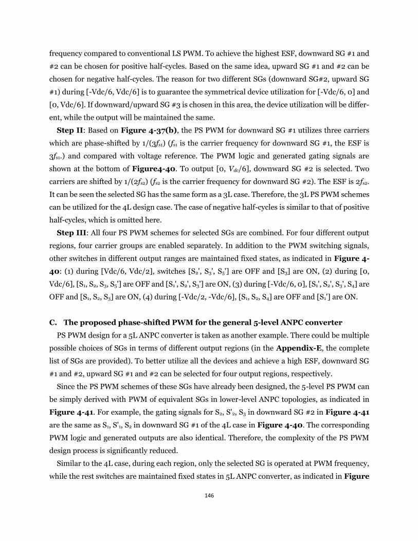
146
frequency compared to conventional LS PWM. To achieve the highest ESF, downward SG #1 and
#2 can be chosen for positive half-cycles. Based on the same idea, upward SG #1 and #2 can be
chosen for negative half-cycles. The reason for two different SGs (downward SG#2, upward SG
#1) during [-Vdc/6, Vdc/6] is to guarantee the symmetrical device utilization for [-Vdc/6, 0] and
[0, Vdc/6]. If downward/upward SG #3 is chosen in this area, the device utilization will be differ-
ent, while the output will be maintained the same.
Step II: Based on Figure 4-37(b), the PS PWM for downward SG #1 utilizes three carriers
which are phase-shifted by 1/(3fs1) (fs1 is the carrier frequency for downward SG #1, the ESF is
3fs1.) and compared with voltage reference. The PWM logic and generated gating signals are
shown at the bottom of Figure4-40. To output [0, Vdc/6], downward SG #2 is selected. Two
carriers are shifted by 1/(2fs2) (fs2 is the carrier frequency for downward SG #2). The ESF is 2fs2.
It can be seen the selected SG has the same form as a 3L case. Therefore, the 3L PS PWM schemes
can be utilized for the 4L design case. The case of negative half-cycles is similar to that of positive
half-cycles, which is omitted here.
Step III: All four PS PWM schemes for selected SGs are combined. For four different output
regions, four carrier groups are enabled separately. In addition to the PWM switching signals,
other switches in different output ranges are maintained fixed states, as indicated in Figure 4-
40: (1) during [Vdc/6, Vdc/2], switches [S2', S3', S5'] are OFF and [S3] are ON, (2) during [0,
Vdc/6], [S1, S2, S3, S5'] are OFF and [S1', S2', S3'] are ON, (3) during [-Vdc/6, 0], [S1', S2', S3', S4] are
OFF and [S1, S2, S3] are ON, (4) during [-Vdc/2, -Vdc/6], [S1, S2, S4] are OFF and [S1'] are ON.
C. The proposed phase-shifted PWM for the general 5-level ANPC converter
PS PWM design for a 5L ANPC converter is taken as another example. There could be multiple
possible choices of SGs in terms of different output regions (in the Appendix-E, the complete
list of SGs are provided). To better utilize all the devices and achieve a high ESF, downward SG
#1 and #2, upward SG #1 and #2 can be selected for four output regions, respectively.
Since the PS PWM schemes of these SGs have already been designed, the 5-level PS PWM can
be simply derived with PWM of equivalent SGs in lower-level ANPC topologies, as indicated in
Figure 4-41. For example, the gating signals for S2, S'2, S3 in downward SG #2 in Figure 4-41
are the same as S1, S'1, S2 in downward SG #1 of the 4L case in Figure 4-40. The corresponding
PWM logic and generated outputs are also identical. Therefore, the complexity of the PS PWM
design process is significantly reduced.
Similar to the 4L case, during each region, only the selected SG is operated at PWM frequency,
while the rest switches are maintained fixed states in 5L ANPC converter, as indicated in Figure
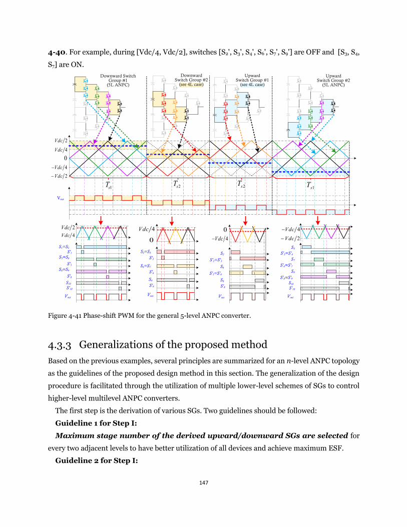
147
4-40. For example, during [Vdc/4, Vdc/2], switches [S2', S3', S4', S6', S7', S9'] are OFF and [S3, S4,
S7] are ON.
2Vdc
Vout
4Vdc04Vdc−
2Vdc−
1sT 2sT 2sT1sT
Downward Switch Group #1
(5L ANPC)
Upward Switch Group #2
(5L ANPC)
Vout
S'1S1=S2
S'8
S'5
S'10
S10
Vout
S'6
S'2
S'9
S9
Vout
S4
S9
S7
S'10
S10
Vout
S5=S6
S8=S9
S2=S3
S6=S7
S'3=S'4
S'6=S'7
S'8=S'9
Upward Switch Group #1
(see 4L case)
Downward Switch Group #2
(see 4L case)
2Vdc4Vdc
0 4Vdc−
2Vdc−
S2
S8
S6
S'2=S'3
S'5=S'6
S'8
4Vdc
0 4Vdc−
Figure 4-41 Phase-shift PWM for the general 5-level ANPC converter.
4.3.3 Generalizations of the proposed method
Based on the previous examples, several principles are summarized for an n-level ANPC topology
as the guidelines of the proposed design method in this section. The generalization of the design
procedure is facilitated through the utilization of multiple lower-level schemes of SGs to control
higher-level multilevel ANPC converters.
The first step is the derivation of various SGs. Two guidelines should be followed:
Guideline 1 for Step I:
Maximum stage number of the derived upward/downward SGs are selected for
every two adjacent levels to have better utilization of all devices and achieve maximum ESF.
Guideline 2 for Step I:
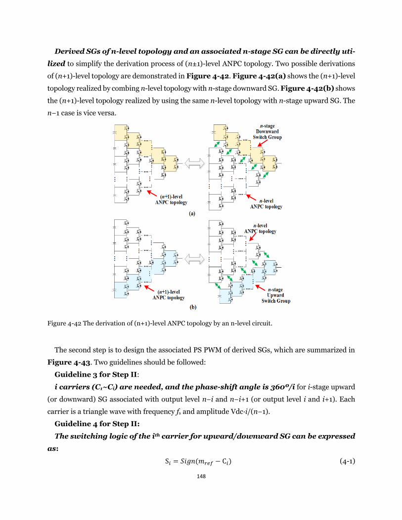
148
Derived SGs of n-level topology and an associated n-stage SG can be directly uti-
lized to simplify the derivation process of (n±1)-level ANPC topology. Two possible derivations
of (n+1)-level topology are demonstrated in Figure 4-42. Figure 4-42(a) shows the (n+1)-level
topology realized by combing n-level topology with n-stage downward SG. Figure 4-42(b) shows
the (n+1)-level topology realized by using the same n-level topology with n-stage upward SG. The
n−1 case is vice versa.
Figure 4-42 The derivation of (n+1)-level ANPC topology by an n-level circuit.
The second step is to design the associated PS PWM of derived SGs, which are summarized in
Figure 4-43. Two guidelines should be followed:
Guideline 3 for Step II:
i carriers (C1~Ci) are needed, and the phase-shift angle is 360º/i for i-stage upward
(or downward) SG associated with output level n−i and n−i+1 (or output level i and i+1). Each
carrier is a triangle wave with frequency fs and amplitude Vdc·i/(n−1).
Guideline 4 for Step II:
The switching logic of the ith carrier for upward/downward SG can be expressed
as:
S𝑖 = 𝑆𝑖𝑔𝑛(𝑚𝑟𝑒𝑓 − C𝑖) (4-1)
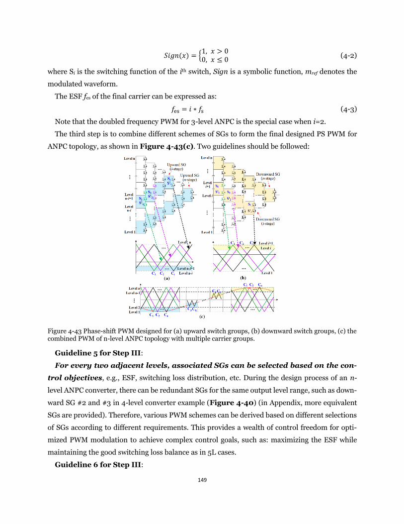
149
𝑆𝑖𝑔𝑛(𝑥) = {1, 𝑥 > 00, 𝑥 ≤ 0
(4-2)
where Si is the switching function of the ith switch, Sign is a symbolic function, mref denotes the
modulated waveform.
The ESF fes of the final carrier can be expressed as:
𝑓es = 𝑖 ∗ 𝑓s (4-3)
Note that the doubled frequency PWM for 3-level ANPC is the special case when i=2.
The third step is to combine different schemes of SGs to form the final designed PS PWM for
ANPC topology, as shown in Figure 4-43(c). Two guidelines should be followed:
Figure 4-43 Phase-shift PWM designed for (a) upward switch groups, (b) downward switch groups, (c) the combined PWM of n-level ANPC topology with multiple carrier groups.
Guideline 5 for Step III:
For every two adjacent levels, associated SGs can be selected based on the con-
trol objectives, e.g., ESF, switching loss distribution, etc. During the design process of an n-
level ANPC converter, there can be redundant SGs for the same output level range, such as down-
ward SG #2 and #3 in 4-level converter example (Figure 4-40) (in Appendix, more equivalent
SGs are provided). Therefore, various PWM schemes can be derived based on different selections
of SGs according to different requirements. This provides a wealth of control freedom for opti-
mized PWM modulation to achieve complex control goals, such as: maximizing the ESF while
maintaining the good switching loss balance as in 5L cases.
Guideline 6 for Step III:
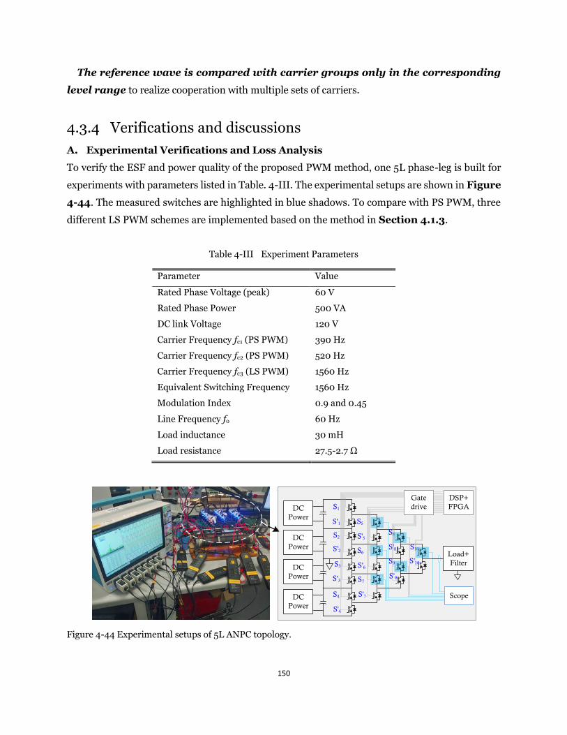
150
The reference wave is compared with carrier groups only in the corresponding
level range to realize cooperation with multiple sets of carriers.
4.3.4 Verifications and discussions
A. Experimental Verifications and Loss Analysis
To verify the ESF and power quality of the proposed PWM method, one 5L phase-leg is built for
experiments with parameters listed in Table. 4-III. The experimental setups are shown in Figure
4-44. The measured switches are highlighted in blue shadows. To compare with PS PWM, three
different LS PWM schemes are implemented based on the method in Section 4.1.3.
Table 4-III Experiment Parameters
Parameter Value
Rated Phase Voltage (peak) 60 V
Rated Phase Power 500 VA
DC link Voltage 120 V
Carrier Frequency fc1 (PS PWM) 390 Hz
Carrier Frequency fc2 (PS PWM) 520 Hz
Carrier Frequency fc3 (LS PWM) 1560 Hz
Equivalent Switching Frequency 1560 Hz
Modulation Index 0.9 and 0.45
Line Frequency fo 60 Hz
Load inductance 30 mH
Load resistance 27.5-2.7 Ω
S'1
S1
S'2
S2
S'3
S3
S'4
S4
S'5
S5
S'6
S6
S'7
S7
S'8
S8
S'9
S9 S'10
S10
DC Power
DC Power
DC Power
DC Power
Load+Filter
10
8
9
Gate drive
DSP+FPGA
Scope
Figure 4-44 Experimental setups of 5L ANPC topology.
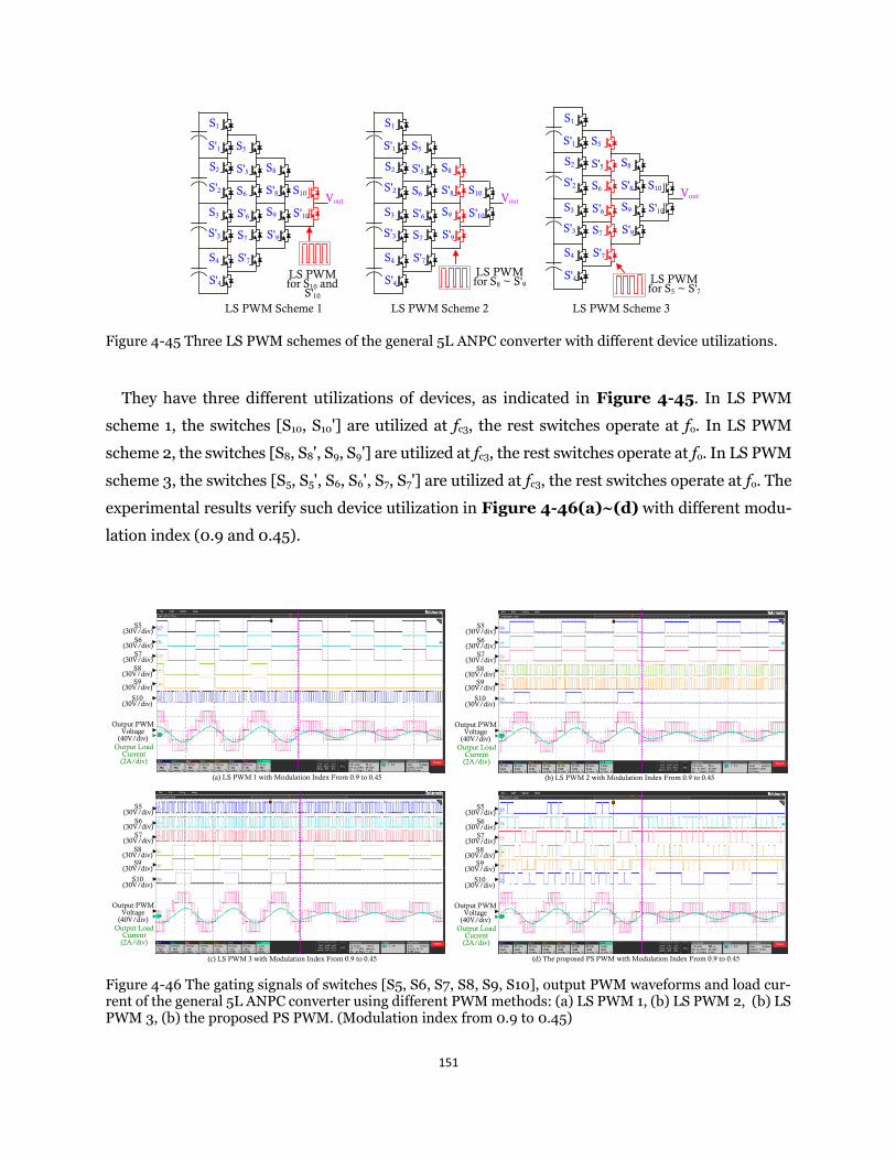
151
S'1
S1
S'2
S2
S'3
S3
S'4
S4
S'5
S5
S'6
S6
S'7
S7
S'8
S8
S'9
S9 S'10
S10 Vout
LS PWM for S10 and
S'10
S'1
S1
S'2
S2
S'3
S3
S'4
S4
S'5
S5
S'6
S6
S'7
S7
S'8
S8
S'9
S9 S'10
S10 Vout
LS PWM for S5 ~ S'7
S'1
S1
S'2
S2
S'3
S3
S'4
S4
S'5
S5
S'6
S6
S'7
S7
S'8
S8
S'9
S9 S'10
S10 Vout
LS PWM for S8 ~ S'9
LS PWM Scheme 1 LS PWM Scheme 2 LS PWM Scheme 3
Figure 4-45 Three LS PWM schemes of the general 5L ANPC converter with different device utilizations.
They have three different utilizations of devices, as indicated in Figure 4-45. In LS PWM
scheme 1, the switches [S10, S10'] are utilized at fc3, the rest switches operate at fo. In LS PWM
scheme 2, the switches [S8, S8', S9, S9'] are utilized at fc3, the rest switches operate at fo. In LS PWM
scheme 3, the switches [S5, S5', S6, S6', S7, S7'] are utilized at fc3, the rest switches operate at fo. The
experimental results verify such device utilization in Figure 4-46(a)~(d) with different modu-
lation index (0.9 and 0.45).
(a) LS PWM 1 with Modulation Index From 0.9 to 0.45
Output PWMVoltage
(40V/div)
S10 (30V/div)
Output Load Current (2A/div)
S9 (30V/div)
S8 (30V/div)
S7 (30V/div)
S6 (30V/div)
S5 (30V/div)
Output PWMVoltage
(40V/div)
S10 (30V/div)
Output Load Current (2A/div)
S9 (30V/div)
S8 (30V/div)
S7 (30V/div)
S6 (30V/div)
S5 (30V/div)
(b) LS PWM 2 with Modulation Index From 0.9 to 0.45
Output PWMVoltage
(40V/div)
S10 (30V/div)
Output Load Current (2A/div)
S9 (30V/div)
S8 (30V/div)
S7 (30V/div)
S6 (30V/div)
S5 (30V/div)
(c) LS PWM 3 with Modulation Index From 0.9 to 0.45
Output PWMVoltage
(40V/div)
S10 (30V/div)
Output Load Current (2A/div)
S9 (30V/div)
S8 (30V/div)
S7 (30V/div)
S6 (30V/div)
S5 (30V/div)
(d) The proposed PS PWM with Modulation Index From 0.9 to 0.45
Figure 4-46 The gating signals of switches [S5, S6, S7, S8, S9, S10], output PWM waveforms and load cur-rent of the general 5L ANPC converter using different PWM methods: (a) LS PWM 1, (b) LS PWM 2, (b) LS PWM 3, (b) the proposed PS PWM. (Modulation index from 0.9 to 0.45)
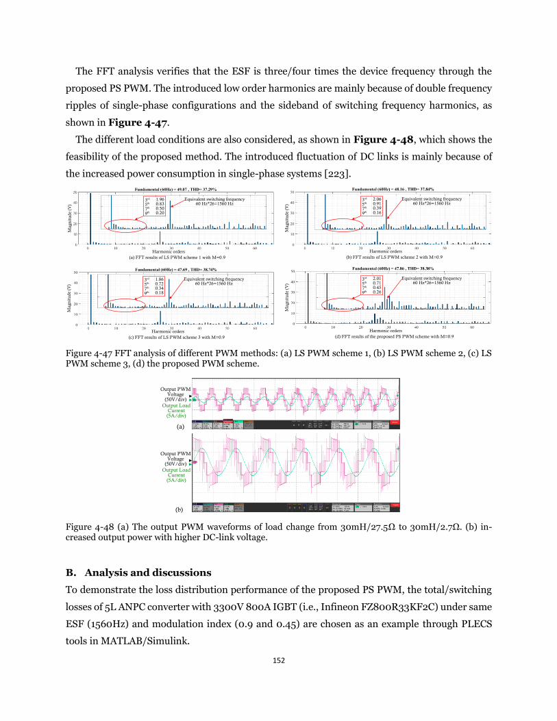
152
The FFT analysis verifies that the ESF is three/four times the device frequency through the
proposed PS PWM. The introduced low order harmonics are mainly because of double frequency
ripples of single-phase configurations and the sideband of switching frequency harmonics, as
shown in Figure 4-47.
The different load conditions are also considered, as shown in Figure 4-48, which shows the
feasibility of the proposed method. The introduced fluctuation of DC links is mainly because of
the increased power consumption in single-phase systems [223].
Equivalent switching frequency60 Hz*26=1560 Hz
3rd 5th 7th 9th
1.96 0.83 0.50 0.20
(a) FFT results of LS PWM scheme 1 with M=0.9
Mag
nitu
de (
V)
Harmonic orders(b) FFT results of LS PWM scheme 2 with M=0.9
Mag
nitu
de (
V)
Harmonic orders
Equivalent switching frequency60 Hz*26=1560 Hz
3rd 5th 7th 9th
2.06 0.91 0.39 0.16
(c) FFT results of LS PWM scheme 3 with M=0.9
Mag
nitu
de (
V)
Harmonic orders
Equivalent switching frequency60 Hz*26=1560 Hz
3rd 5th 7th 9th
1.86 0.72 0.34 0.18
(d) FFT results of the proposed PS PWM scheme with M=0.9
Mag
nitu
de (
V)
Harmonic orders
Equivalent switching frequency60 Hz*26=1560 Hz
3rd 5th 7th 9th
2.01 0.71 0.45 0.26
Figure 4-47 FFT analysis of different PWM methods: (a) LS PWM scheme 1, (b) LS PWM scheme 2, (c) LS PWM scheme 3, (d) the proposed PWM scheme.
Output PWMVoltage
(50V/div)Output Load
Current (5A/div)
(a)
Output PWMVoltage
(50V/div)Output Load
Current (5A/div)
(b)
Figure 4-48 (a) The output PWM waveforms of load change from 30mH/27.5Ω to 30mH/2.7Ω. (b) in-creased output power with higher DC-link voltage.
B. Analysis and discussions
To demonstrate the loss distribution performance of the proposed PS PWM, the total/switching
losses of 5L ANPC converter with 3300V 800A IGBT (i.e., Infineon FZ800R33KF2C) under same
ESF (1560Hz) and modulation index (0.9 and 0.45) are chosen as an example through PLECS
tools in MATLAB/Simulink.
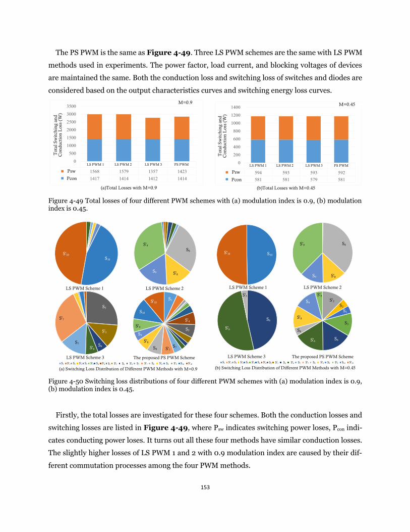
153
The PS PWM is the same as Figure 4-49. Three LS PWM schemes are the same with LS PWM
methods used in experiments. The power factor, load current, and blocking voltages of devices
are maintained the same. Both the conduction loss and switching loss of switches and diodes are
considered based on the output characteristics curves and switching energy loss curves.
1 2 3 4Series2 1568 1579 1357 1423Series1 1417 1414 1412 1414
0
500
1000
1500
2000
2500
3000
3500
Psw
Pcon
Tot
al S
wit
chin
g an
d
Con
duct
ion
Los
s (W
)
LS PWM 1 LS PWM 2 LS PWM 3 PS PWM
M=0.9
(a)Total Losses with M=0.9
1 2 3 4Series2 594 593 593 592Series1 581 581 579 581
0
200
400
600
800
1000
1200
1400
Psw
Pcon
Tot
al S
wit
chin
g an
d
Con
duct
ion
Los
s (W
)
LS PWM 1 LS PWM 2 LS PWM 3 PS PWM
M=0.45
(b)Total Losses with M=0.45
Figure 4-49 Total losses of four different PWM schemes with (a) modulation index is 0.9, (b) modulation index is 0.45.
1 2 3 4 5 6 7 8 9 10 11 12 13 14 15 16 17 18 19 20S'10S10S'9S9S'8S8S'7S7S'6S6S'5S5S'1S1 S'2S2 S'3S3 S'4S4
(a) Switching Loss Distribution of Different PWM Methods with
S'10
S10
S'9
S9
S'8S8 S'7
S5
S'4
S1
S7
S5
S'5
S'6S6
S9
S7
S'7
S'9
S'8
S8
S9
S'10
S10
LS PWM Scheme 1 LS PWM Scheme 2
LS PWM Scheme 3 The proposed PS PWM Scheme
M=0.9
1 2 3 4 5 6 7 8 9 10 11 12 13 14 15 16 17 18 19 20S'10S10S'9S9S'8S8S'7S7S'6S6S'5S5S'1S1 S'2S2 S'3S3 S'4S4
(b) Switching Loss Distribution of Different PWM Methods with
S9
S'5
S'6
S6
S'9
S'8
S8
S9
S'10 S10
LS PWM Scheme 1 LS PWM Scheme 2
LS PWM Scheme 3 The proposed PS PWM Scheme
M=0.45
S8
S'8
S'6 S6
S9
S3
S3
S2
S'2S'9
Figure 4-50 Switching loss distributions of four different PWM schemes with (a) modulation index is 0.9, (b) modulation index is 0.45.
Firstly, the total losses are investigated for these four schemes. Both the conduction losses and
switching losses are listed in Figure 4-49, where Psw indicates switching power loses, Pcon indi-
cates conducting power loses. It turns out all these four methods have similar conduction losses.
The slightly higher losses of LS PWM 1 and 2 with 0.9 modulation index are caused by their dif-
ferent commutation processes among the four PWM methods.
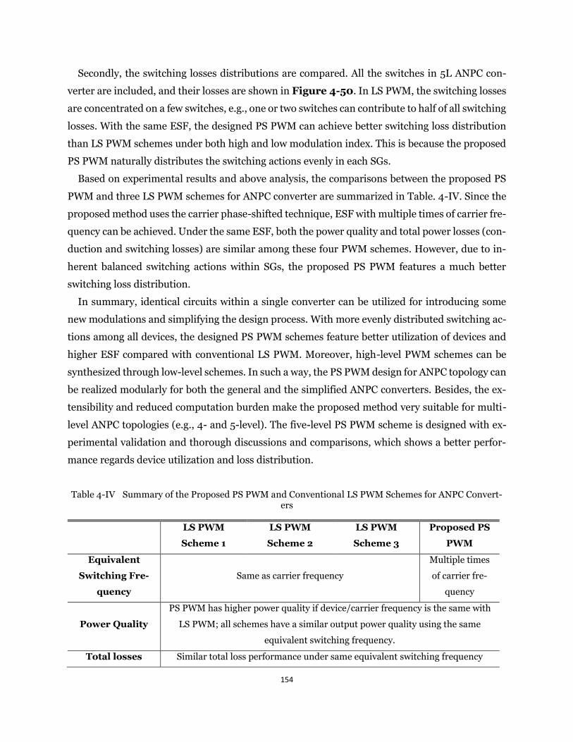
154
Secondly, the switching losses distributions are compared. All the switches in 5L ANPC con-
verter are included, and their losses are shown in Figure 4-50. In LS PWM, the switching losses
are concentrated on a few switches, e.g., one or two switches can contribute to half of all switching
losses. With the same ESF, the designed PS PWM can achieve better switching loss distribution
than LS PWM schemes under both high and low modulation index. This is because the proposed
PS PWM naturally distributes the switching actions evenly in each SGs.
Based on experimental results and above analysis, the comparisons between the proposed PS
PWM and three LS PWM schemes for ANPC converter are summarized in Table. 4-IV. Since the
proposed method uses the carrier phase-shifted technique, ESF with multiple times of carrier fre-
quency can be achieved. Under the same ESF, both the power quality and total power losses (con-
duction and switching losses) are similar among these four PWM schemes. However, due to in-
herent balanced switching actions within SGs, the proposed PS PWM features a much better
switching loss distribution.
In summary, identical circuits within a single converter can be utilized for introducing some
new modulations and simplifying the design process. With more evenly distributed switching ac-
tions among all devices, the designed PS PWM schemes feature better utilization of devices and
higher ESF compared with conventional LS PWM. Moreover, high-level PWM schemes can be
synthesized through low-level schemes. In such a way, the PS PWM design for ANPC topology can
be realized modularly for both the general and the simplified ANPC converters. Besides, the ex-
tensibility and reduced computation burden make the proposed method very suitable for multi-
level ANPC topologies (e.g., 4- and 5-level). The five-level PS PWM scheme is designed with ex-
perimental validation and thorough discussions and comparisons, which shows a better perfor-
mance regards device utilization and loss distribution.
Table 4-IV Summary of the Proposed PS PWM and Conventional LS PWM Schemes for ANPC Convert-ers
LS PWM
Scheme 1
LS PWM
Scheme 2
LS PWM
Scheme 3
Proposed PS
PWM
Equivalent
Switching Fre-
quency
Same as carrier frequency
Multiple times
of carrier fre-
quency
Power Quality
PS PWM has higher power quality if device/carrier frequency is the same with
LS PWM; all schemes have a similar output power quality using the same
equivalent switching frequency.
Total losses Similar total loss performance under same equivalent switching frequency
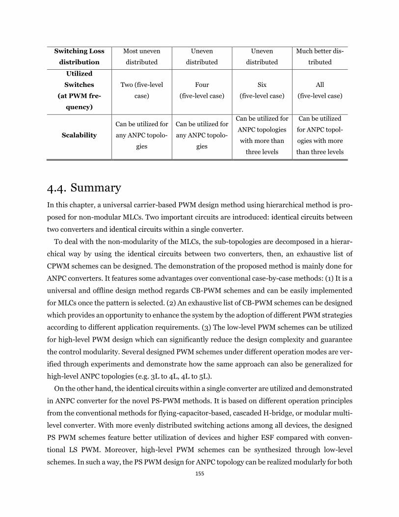
155
Switching Loss
distribution
Most uneven
distributed
Uneven
distributed
Uneven
distributed
Much better dis-
tributed
Utilized
Switches
(at PWM fre-
quency)
Two (five-level
case)
Four
(five-level case)
Six
(five-level case)
All
(five-level case)
Scalability
Can be utilized for
any ANPC topolo-
gies
Can be utilized for
any ANPC topolo-
gies
Can be utilized for
ANPC topologies
with more than
three levels
Can be utilized
for ANPC topol-
ogies with more
than three levels
4.4. Summary
In this chapter, a universal carrier-based PWM design method using hierarchical method is pro-
posed for non-modular MLCs. Two important circuits are introduced: identical circuits between
two converters and identical circuits within a single converter.
To deal with the non-modularity of the MLCs, the sub-topologies are decomposed in a hierar-
chical way by using the identical circuits between two converters, then, an exhaustive list of
CPWM schemes can be designed. The demonstration of the proposed method is mainly done for
ANPC converters. It features some advantages over conventional case-by-case methods: (1) It is a
universal and offline design method regards CB-PWM schemes and can be easily implemented
for MLCs once the pattern is selected. (2) An exhaustive list of CB-PWM schemes can be designed
which provides an opportunity to enhance the system by the adoption of different PWM strategies
according to different application requirements. (3) The low-level PWM schemes can be utilized
for high-level PWM design which can significantly reduce the design complexity and guarantee
the control modularity. Several designed PWM schemes under different operation modes are ver-
ified through experiments and demonstrate how the same approach can also be generalized for
high-level ANPC topologies (e.g. 3L to 4L, 4L to 5L).
On the other hand, the identical circuits within a single converter are utilized and demonstrated
in ANPC converter for the novel PS-PWM methods. It is based on different operation principles
from the conventional methods for flying-capacitor-based, cascaded H-bridge, or modular multi-
level converter. With more evenly distributed switching actions among all devices, the designed
PS PWM schemes feature better utilization of devices and higher ESF compared with conven-
tional LS PWM. Moreover, high-level PWM schemes can be synthesized through low-level
schemes. In such a way, the PS PWM design for ANPC topology can be realized modularly for both
156
the general and the simplified ANPC converters. Besides, the extensibility and reduced computa-
tion burden make the proposed method very suitable for multi-level ANPC topologies (e.g., 4- and
5-level). The five-level PS PWM scheme is designed with experimental validation and thorough
discussions and comparisons, which shows a better performance regards device utilization and
loss distribution.
In addition to ANPC converters, the implementation of hierarchical concepts can also poten-
tially facilitate the PWM design process for other non-modular MLCs, especially those ANPC-
based derivatives. In the next chapter, the proposed PWM design method in this chapter will be
synergically combined with the unified matrix models in chapter 3 for some specialized issues
of ANPC converters.
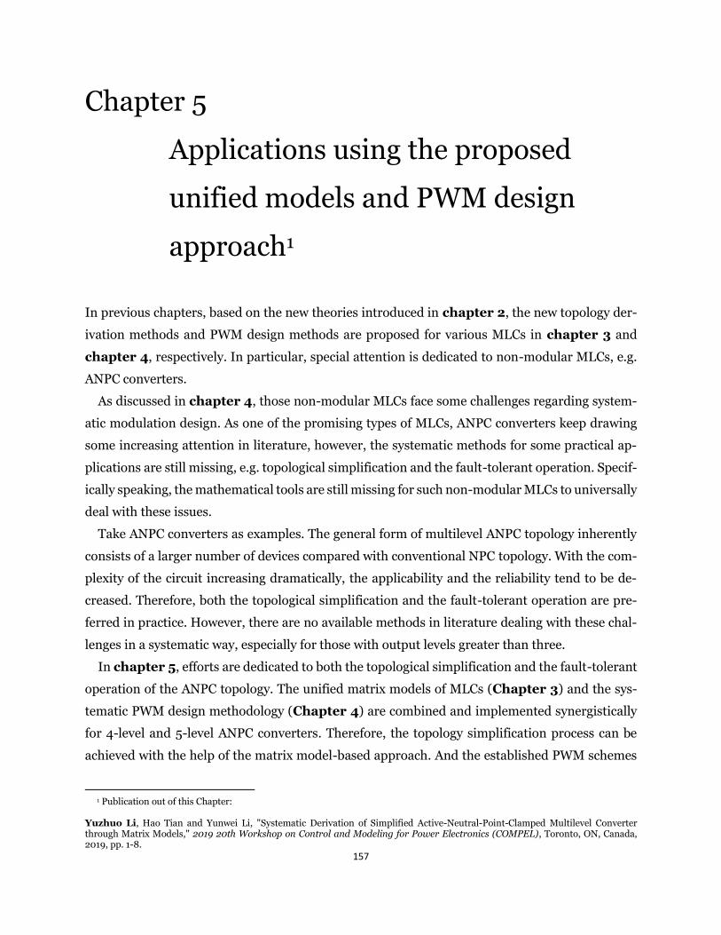
157
Chapter 5 Applications using the proposed
unified models and PWM design
approach1
In previous chapters, based on the new theories introduced in chapter 2, the new topology der-
ivation methods and PWM design methods are proposed for various MLCs in chapter 3 and
chapter 4, respectively. In particular, special attention is dedicated to non-modular MLCs, e.g.
ANPC converters.
As discussed in chapter 4, those non-modular MLCs face some challenges regarding system-
atic modulation design. As one of the promising types of MLCs, ANPC converters keep drawing
some increasing attention in literature, however, the systematic methods for some practical ap-
plications are still missing, e.g. topological simplification and the fault-tolerant operation. Specif-
ically speaking, the mathematical tools are still missing for such non-modular MLCs to universally
deal with these issues.
Take ANPC converters as examples. The general form of multilevel ANPC topology inherently
consists of a larger number of devices compared with conventional NPC topology. With the com-
plexity of the circuit increasing dramatically, the applicability and the reliability tend to be de-
creased. Therefore, both the topological simplification and the fault-tolerant operation are pre-
ferred in practice. However, there are no available methods in literature dealing with these chal-
lenges in a systematic way, especially for those with output levels greater than three.
In chapter 5, efforts are dedicated to both the topological simplification and the fault-tolerant
operation of the ANPC topology. The unified matrix models of MLCs (Chapter 3) and the sys-
tematic PWM design methodology (Chapter 4) are combined and implemented synergistically
for 4-level and 5-level ANPC converters. Therefore, the topology simplification process can be
achieved with the help of the matrix model-based approach. And the established PWM schemes
1 Publication out of this Chapter:
Yuzhuo Li, Hao Tian and Yunwei Li, "Systematic Derivation of Simplified Active-Neutral-Point-Clamped Multilevel Converter through Matrix Models," 2019 20th Workshop on Control and Modeling for Power Electronics (COMPEL), Toronto, ON, Canada, 2019, pp. 1-8.
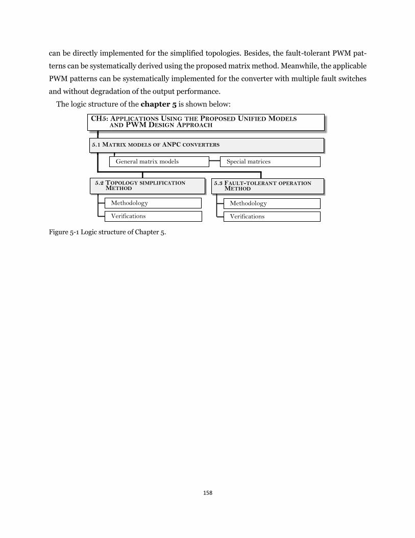
158
can be directly implemented for the simplified topologies. Besides, the fault-tolerant PWM pat-
terns can be systematically derived using the proposed matrix method. Meanwhile, the applicable
PWM patterns can be systematically implemented for the converter with multiple fault switches
and without degradation of the output performance.
The logic structure of the chapter 5 is shown below:
Special matrices
CH5: APPLICATIONS USING THE PROPOSED UNIFIED MODELS AND PWM DESIGN APPROACH
5.1 MATRIX MODELS OF ANPC CONVERTERS
Methodology
Verifications
5.3 FAULT-TOLERANT OPERATION METHOD
Methodology
Verifications
5.2 TOPOLOGY SIMPLIFICATION METHOD
General matrix models
Figure 5-1 Logic structure of Chapter 5.
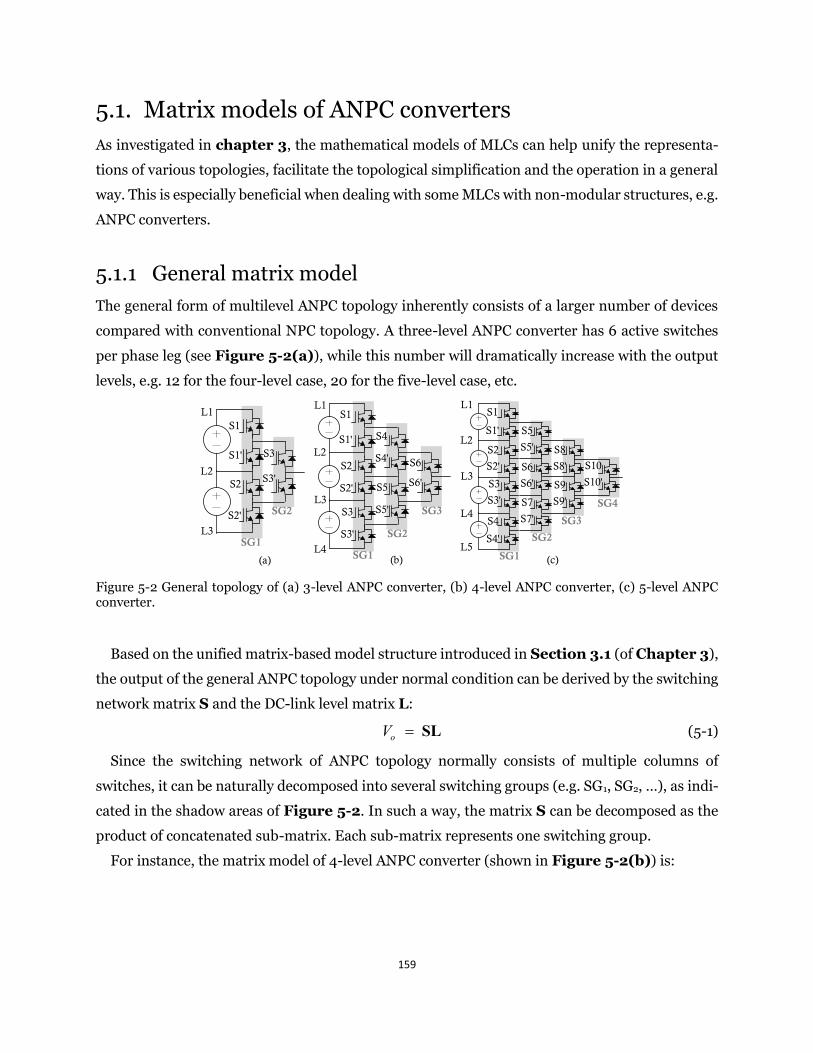
159
5.1. Matrix models of ANPC converters
As investigated in chapter 3, the mathematical models of MLCs can help unify the representa-
tions of various topologies, facilitate the topological simplification and the operation in a general
way. This is especially beneficial when dealing with some MLCs with non-modular structures, e.g.
ANPC converters.
5.1.1 General matrix model
The general form of multilevel ANPC topology inherently consists of a larger number of devices
compared with conventional NPC topology. A three-level ANPC converter has 6 active switches
per phase leg (see Figure 5-2(a)), while this number will dramatically increase with the output
levels, e.g. 12 for the four-level case, 20 for the five-level case, etc.
S1
S1'
S2
S2'
S3
S3'
S4
S4'
S5
S5'
S6
S6'
(a)
S1
S1'
S2
S2'
S3
S3'
S4
S4'
S5
S5'
S6
S6'
S7
S7'
S8
S8'
S9
S9'
S10
S10'
(b) (c)
S1
S1'
S2
S2'
S3
S3'
L1
L2
L3
L1
L2
L3
L4
L1
L2
L3
L4
L5SG1
SG2
SG3
SG4
SG1
SG2
SG3
SG1
SG2
Figure 5-2 General topology of (a) 3-level ANPC converter, (b) 4-level ANPC converter, (c) 5-level ANPC converter.
Based on the unified matrix-based model structure introduced in Section 3.1 (of Chapter 3),
the output of the general ANPC topology under normal condition can be derived by the switching
network matrix S and the DC-link level matrix L:
oV = SL (5-1)
Since the switching network of ANPC topology normally consists of multiple columns of
switches, it can be naturally decomposed into several switching groups (e.g. SG1, SG2, …), as indi-
cated in the shadow areas of Figure 5-2. In such a way, the matrix S can be decomposed as the
product of concatenated sub-matrix. Each sub-matrix represents one switching group.
For instance, the matrix model of 4-level ANPC converter (shown in Figure 5-2(b)) is:
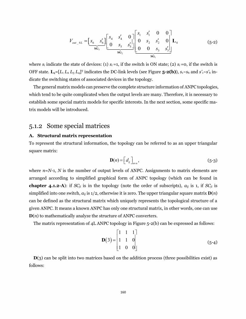
160
3
2
1
1 14 4
_ 4 6 6 2 2 45 5
3 3
0 00
0 00
0 0out L
s ss s
V s s s ss s
s s
= SG
SGSG
L (5-2)
where si indicate the state of devices: (1) si =1, if the switch is ON state; (2) si =0, if the switch is
OFF state. L4=[L1 L2 L3 L4]T indicates the DC-link levels (see Figure 5-2(b)), s1~s6 and s'1~s'6 in-
dicate the switching states of associated devices in the topology.
The general matrix models can preserve the complete structure information of ANPC topologies,
which tend to be quite complicated when the output levels are many. Therefore, it is necessary to
establish some special matrix models for specific interests. In the next section, some specific ma-
trix models will be introduced.
5.1.2 Some special matrices
A. Structural matrix representation
To represent the structural information, the topology can be referred to as an upper triangular
square matrix:
( ) ij n nn d
= D , (5-3)
where n=N-1, N is the number of output levels of ANPC. Assignments to matrix elements are
arranged according to simplified graphical form of ANPC topology (which can be found in
chapter 4.1.2-A): if SCji is in the topology (note the order of subscripts), aij is 1, if SCji is
simplified into one switch, aij is 1/2, otherwise it is zero. The upper triangular square matrix D(n)
can be defined as the structural matrix which uniquely represents the topological structure of a
given ANPC. It means a known ANPC has only one structural matrix, in other words, one can use
D(n) to mathematically analyze the structure of ANPC converters.
The matrix representation of 4L ANPC topology in Figure 5-2(b) can be expressed as follows:
(5-4)
D(3) can be split into two matrices based on the addition process (three possibilities exist) as
follows:
( )
1 1 13 1 1 0
1 0 0
=
D
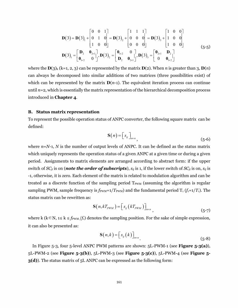
161
(5-5)
where the D(3)k (k=1, 2, 3) can be represented by the matrix D(2). When n is greater than 3, D(n)
can always be decomposed into similar additions of two matrices (three possibilities exist) of
which can be represented by the matrix D(n-1). The equivalent iteration process can continue
until n=2, which is essentially the matrix representation of the hierarchical decomposition process
introduced in Chapter 4.
B. Status matrix representation
To represent the possible operation status of ANPC converter, the following square matrix can be
defined:
, (5-6)
where n=N-1, N is the number of output levels of ANPC. It can be defined as the status matrix
which uniquely represents the operation status of a given ANPC at a given time or during a given
period. Assignments to matrix elements are arranged according to abstract form: if the upper
switch of SCji is on (note the order of subscripts), sij is 1, if the lower switch of SCji is on, sij is
-1, otherwise, it is zero. Each element of the matrix is related to modulation algorithm and can be
treated as a discrete function of the sampling period TPWM (assuming the algorithm is regular
sampling PWM, sample frequency is fPWM=1/TPWM) and the fundamental period T1 (f1=1/T1). The
status matrix can be rewritten as:
, (5-7)
where k (k∈N, 1≤ k ≤ fPWM /f1) denotes the sampling position. For the sake of simple expression,
it can also be presented as:
. (5-8)
In Figure 5-3, four 5-level ANPC PWM patterns are shown: 5L-PWM-1 (see Figure 5-3(a)),
5L-PWM-2 (see Figure 5-3(b)), 5L-PWM-3 (see Figure 5-3(c)), 5L-PWM-4 (see Figure 5-
3(d)). The status matrix of 5L ANPC can be expressed as the following form:
( ) ( ) ( ) ( )
( ) ( ) ( )
1 2 3
2 2 1 1 2 2 1 21 2 3
1 2 2 2 1 1 2
0 0 1 1 1 1 1 0 03 3 0 1 0 3 0 0 0 3 1 0 0
1 0 0 0 0 0 1 0 0
03 , 3 , 3
0 0
= + = + = +
= = =
D D D D
D 0 0 0 DD D D
0 D 0 0
( ) ij n nn s
= S
( ) ( ), PWM ij PWM n nn kT s kT
= S
( ) ( ), ij n nn k s k
= S
162
( )
( ) ( ) ( ) ( )
( ) ( ) ( )
( ) ( )
( )
11 12 13 14
21 22 23
31 32
41
04,
0 00 0 0
s k s k s k s ks k s k s k
ks k s ks k
=
S (5-9)
To simplify the expression, it can be written in the column vector form:
( ) ( ) ( ) ( ) ( )1 2 3 44, g g g gk k k k k = S s s s s
he expression, it can be written in the column vector form:
( ) ( ) ( ) ( ) ( ) ( ) ( ) ( ) ( ) ( )( ) ( ) ( ) ( ) ( )k k k k k( ) ( ) ( ) ( ) ( ) ( ) ( ) ( ) ( ) ( )k k k k k( ) ( ) ( ) ( ) ( ) ( ) ( ) ( ) ( ) ( ) ( ) ( ) ( ) ( ) ( ) ( ) ( ) ( ) ( ) ( ) ( ) ( ) ( ) ( ) ( )( ) ( ) ( ) ( ) ( )k k k k k( ) ( ) ( ) ( ) ( ) ( ) ( ) ( ) ( ) ( )k k k k k( ) ( ) ( ) ( ) ( ) ( ) ( ) ( ) ( ) ( )k k k k k( ) ( ) ( ) ( ) ( ) ( ) ( ) ( ) ( ) ( )k k k k k( ) ( ) ( ) ( ) ( )( ) ( ) ( ) ( ) ( )4( ) ( ) ( ) ( ) ( )k k k k k( ) ( ) ( ) ( ) ( )4( ) ( ) ( ) ( ) ( ) ( ) ( ) ( ) ( ) ( )4( ) ( ) ( ) ( ) ( )k k k k k( ) ( ) ( ) ( ) ( )4( ) ( ) ( ) ( ) ( ) ( ) ( ) ( ) ( ) ( )4( ) ( ) ( ) ( ) ( )k k k k k( ) ( ) ( ) ( ) ( )4( ) ( ) ( ) ( ) ( ) ( ) ( ) ( ) ( ) ( )4( ) ( ) ( ) ( ) ( )k k k k k( ) ( ) ( ) ( ) ( )4( ) ( ) ( ) ( ) ( )( ) ( ) ( ) ( ) ( )k k k k k( ) ( ) ( ) ( ) ( ) ( ) ( ) ( ) ( ) ( )k k k k k( ) ( ) ( ) ( ) ( )S s s s s( ) ( ) ( ) ( ) ( )k k k k k( ) ( ) ( ) ( ) ( ) ( ) ( ) ( ) ( ) ( )k k k k k( ) ( ) ( ) ( ) ( )( ) ( ) ( ) ( ) ( )k k k k k( ) ( ) ( ) ( ) ( ) ( ) ( ) ( ) ( ) ( )k k k k k( ) ( ) ( ) ( ) ( ) ( ) ( ) ( ) ( ) ( )k k k k k( ) ( ) ( ) ( ) ( ) ( ) ( ) ( ) ( ) ( )k k k k k( ) ( ) ( ) ( ) ( )S s s s s( ) ( ) ( ) ( ) ( )k k k k k( ) ( ) ( ) ( ) ( ) ( ) ( ) ( ) ( ) ( )k k k k k( ) ( ) ( ) ( ) ( ) ( ) ( ) ( ) ( ) ( )k k k k k( ) ( ) ( ) ( ) ( ) ( ) ( ) ( ) ( ) ( )k k k k k( ) ( ) ( ) ( ) ( )( ) ( ) ( ) ( ) ( )1( ) ( ) ( ) ( ) ( )k k k k k( ) ( ) ( ) ( ) ( )1( ) ( ) ( ) ( ) ( ) ( ) ( ) ( ) ( ) ( )1( ) ( ) ( ) ( ) ( )k k k k k( ) ( ) ( ) ( ) ( )1( ) ( ) ( ) ( ) ( ) ( ) ( ) ( ) ( ) ( )1( ) ( ) ( ) ( ) ( )k k k k k( ) ( ) ( ) ( ) ( )1( ) ( ) ( ) ( ) ( ) ( ) ( ) ( ) ( ) ( )1( ) ( ) ( ) ( ) ( )k k k k k( ) ( ) ( ) ( ) ( )1( ) ( ) ( ) ( ) ( )S s s s s( ) ( ) ( ) ( ) ( )1( ) ( ) ( ) ( ) ( )k k k k k( ) ( ) ( ) ( ) ( )1( ) ( ) ( ) ( ) ( ) ( ) ( ) ( ) ( ) ( )1( ) ( ) ( ) ( ) ( )k k k k k( ) ( ) ( ) ( ) ( )1( ) ( ) ( ) ( ) ( ) ( ) ( ) ( ) ( ) ( )1( ) ( ) ( ) ( ) ( )k k k k k( ) ( ) ( ) ( ) ( )1( ) ( ) ( ) ( ) ( ) ( ) ( ) ( ) ( ) ( )1( ) ( ) ( ) ( ) ( )k k k k k( ) ( ) ( ) ( ) ( )1( ) ( ) ( ) ( ) ( )( ) ( ) ( ) ( ) ( )2( ) ( ) ( ) ( ) ( )k k k k k( ) ( ) ( ) ( ) ( )2( ) ( ) ( ) ( ) ( ) ( ) ( ) ( ) ( ) ( )2( ) ( ) ( ) ( ) ( )k k k k k( ) ( ) ( ) ( ) ( )2( ) ( ) ( ) ( ) ( ) ( ) ( ) ( ) ( ) ( )2( ) ( ) ( ) ( ) ( )k k k k k( ) ( ) ( ) ( ) ( )2( ) ( ) ( ) ( ) ( ) ( ) ( ) ( ) ( ) ( )2( ) ( ) ( ) ( ) ( )k k k k k( ) ( ) ( ) ( ) ( )2( ) ( ) ( ) ( ) ( )S s s s s( ) ( ) ( ) ( ) ( )2( ) ( ) ( ) ( ) ( )k k k k k( ) ( ) ( ) ( ) ( )2( ) ( ) ( ) ( ) ( ) ( ) ( ) ( ) ( ) ( )2( ) ( ) ( ) ( ) ( )k k k k k( ) ( ) ( ) ( ) ( )2( ) ( ) ( ) ( ) ( ) ( ) ( ) ( ) ( ) ( )2( ) ( ) ( ) ( ) ( )k k k k k( ) ( ) ( ) ( ) ( )2( ) ( ) ( ) ( ) ( ) ( ) ( ) ( ) ( ) ( )2( ) ( ) ( ) ( ) ( )k k k k k( ) ( ) ( ) ( ) ( )2( ) ( ) ( ) ( ) ( )( ) ( ) ( ) ( ) ( )3( ) ( ) ( ) ( ) ( )k k k k k( ) ( ) ( ) ( ) ( )3( ) ( ) ( ) ( ) ( ) ( ) ( ) ( ) ( ) ( )3( ) ( ) ( ) ( ) ( )k k k k k( ) ( ) ( ) ( ) ( )3( ) ( ) ( ) ( ) ( ) ( ) ( ) ( ) ( ) ( )3( ) ( ) ( ) ( ) ( )k k k k k( ) ( ) ( ) ( ) ( )3( ) ( ) ( ) ( ) ( ) ( ) ( ) ( ) ( ) ( )3( ) ( ) ( ) ( ) ( )k k k k k( ) ( ) ( ) ( ) ( )3( ) ( ) ( ) ( ) ( )S s s s s( ) ( ) ( ) ( ) ( )3( ) ( ) ( ) ( ) ( )k k k k k( ) ( ) ( ) ( ) ( )3( ) ( ) ( ) ( ) ( ) ( ) ( ) ( ) ( ) ( )3( ) ( ) ( ) ( ) ( )k k k k k( ) ( ) ( ) ( ) ( )3( ) ( ) ( ) ( ) ( ) ( ) ( ) ( ) ( ) ( )3( ) ( ) ( ) ( ) ( )k k k k k( ) ( ) ( ) ( ) ( )3( ) ( ) ( ) ( ) ( ) ( ) ( ) ( ) ( ) ( )3( ) ( ) ( ) ( ) ( )k k k k k( ) ( ) ( ) ( ) ( )3( ) ( ) ( ) ( ) ( ) (5-10)
where ( )gi ks ( )gi ( )k( )s
denotes the status vector form of ith SG, i=1,2,3,4.
SC41
SC23
SC14
SC23
SC14
SC23
SC14
SC11
SC12
SC22
SC13
SC21
SC31
SC11
SC12
SC22
SC13
SC21
SC31
SG1
SG2
SG3
SG1
SG2
SG3
SC11
SC12
SC22
SC13
SC21
SC31
SG1
SG2
SG3
SC41 SC41
SG4 SG4 SG4 SC23
SC14
SC11
SC12
SC22
SC13
SC21
SC31
SG2
SG3
SC41
SG4
SG1 (d)(c)(b)(a)
SC32 SC32 SC32 SC32
Figure 5-3 5-level ANPC PWM patterns. (a) 5L-PWM-1, (b) 5L-PWM-2, (c) 5L-PWM-3, (d) 5L-PWM-4.
2Vdc
refU4
Vdc
4Vdc
−
2Vdc
−
( )1g PWMkTs (1g PWM(g PWM(1g PWM1 kTg PWMkTg PWMs
( )1sin 2A f
( )2g PWMkTs ( )2g PWM( )g PWM( )2g PWM2 ( )kT( )( )g PWM( )kT( )g PWM( )s
( )3g PWMkTs (3g PWM(g PWM(3g PWM3 kTg PWMkTg PWMs
( )4g PWMkTs ( )4g PWM( )g PWM( )4g PWM4 ( )kT( )( )g PWM( )kT( )g PWM( )s
1SGV
2SGV
3SGV
4SGV
refU
PWMV
PWMV
(a) (b)
( )1sin 2A f
2Vdc
2Vdc
−
Figure 5-4 The carrier-based PWM generation and associated switching status of the upper switch of each SCs (same SG) of 5L-PWM-1. (a) value of one element in each status vectors, (b) blocking voltages in simu-lation.
The carrier-based PWM generation and associated switching status of the upper switch of each
SCs (same SG) of 5L-PWM-1 are shown in Figure 5-4. Note that, in each status vector (represents
the status of SG), all elements (represent the status of SCs) are expected to have the same value at
the same time based on 5L-PWM-1, which gives:
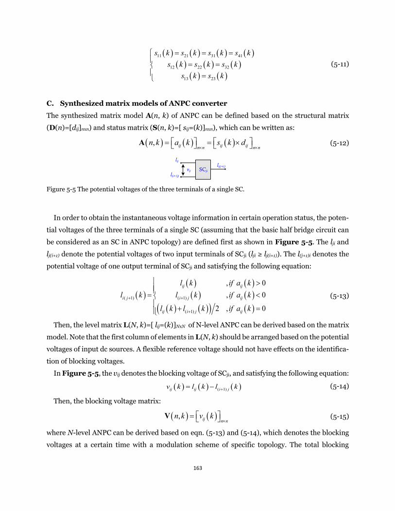
163
( ) ( ) ( ) ( )
( ) ( ) ( )
( ) ( )
11 21 31 41
12 22 32
13 23
s k s k s k s ks k s k s k
s k s k
= = =
= = =
(5-11)
C. Synthesized matrix models of ANPC converter
The synthesized matrix model A(n, k) of ANPC can be defined based on the structural matrix
(D(n)=[dij]nxn) and status matrix (S(n, k)=[ sij=(k)]nxn), which can be written as:
( ) ( ) ( ), ij ij ijn n n nn k a k s k d
= = A (5-12)
SCji
lij
l(i+1)j
li(j+1)vij
Figure 5-5 The potential voltages of the three terminals of a single SC.
In order to obtain the instantaneous voltage information in certain operation status, the poten-
tial voltages of the three terminals of a single SC (assuming that the basic half bridge circuit can
be considered as an SC in ANPC topology) are defined first as shown in Figure 5-5. The lji and
lj(i+1) denote the potential voltages of two input terminals of SCji (lji ≥ lj(i+1)). The l(j+1)i denotes the
potential voltage of one output terminal of SCji and satisfying the following equation:
( )
( ) ( )
( ) ( )
( ) ( )( ) ( )
( 1) ( 1)
( 1)
, 0, 0
2 , 0
ij ij
i j i j ij
ij i j ij
l k if a kl k l k if a k
l k l k if a k+ +
+
=
+ =
(5-13)
Then, the level matrix L(N, k)=[ lij=(k)]NxN of N-level ANPC can be derived based on the matrix
model. Note that the first column of elements in L(N, k) should be arranged based on the potential
voltages of input dc sources. A flexible reference voltage should not have effects on the identifica-
tion of blocking voltages.
In Figure 5-5, the vij denotes the blocking voltage of SCji, and satisfying the following equation:
( ) ( ) ( )( 1)ij ij i jv k l k l k+= − (5-14)
Then, the blocking voltage matrix:
( ) ( ), ij n nn k v k
= V (5-15)
where N-level ANPC can be derived based on eqn. (5-13) and (5-14), which denotes the blocking
voltages at a certain time with a modulation scheme of specific topology. The total blocking
164
voltage Vtotal (k) of the N-level ANPC at time k can be calculated based on the sum of all elements
of blocking voltage matrix as follows:
( )1 1
n n
jtota ilj i
V kv= =
= (5-16)
5.1.3 5L ANPC example
Here using an example of 5L ANPC to demonstrate the whole process. The status matrix at a cer-
tain time kt2 is assumed to be:
( ) ( )2 2 4 4
1 1 1 11 1 1 0
4,1 1 0 01 0 0 0
t ij tk s k
−
− = = −
S (5-17)
Then, the matrix model is
( ) ( ) ( ) ( )2 2 2 24 4 4 44, 4,t ij t ij t ij tk a k s k d k
= = = A S (5-18)
Based on (5-13), the level matrix can be obtained:
( ) ( )2 2 5 5
5 5 5 5 34 4 3 3 0
5, 3 3 3 0 02 0 0 0
0 0 0 0
t ij t
E E E E EE E E E
k l k E E EE E
E
= =
L (5-19)
Note that the first column of elements of L(5, kt2) are arranged according to possible potential
voltages of input dc sources (assuming the lowest potential voltage is E).
Based on (8) and (12), the blocking voltage matrix can be obtained:
( ) ( )2 2 4 4
2 20 0
4,2 0 00 0 0
t ij t
E E E EE E
k v kE EE
= =
V (5-20)
which indicates that the blocking voltages are E for SC11~SC14 and SC21~SC22, 2E for SC23, SC31 and
SC41, zero for SC32. While the high blocking voltage is undesired in practice and should be avoided.
This process can also be achieved by manual operation of the level matrix. The process can be
expressed as (5-21) and (5-22).
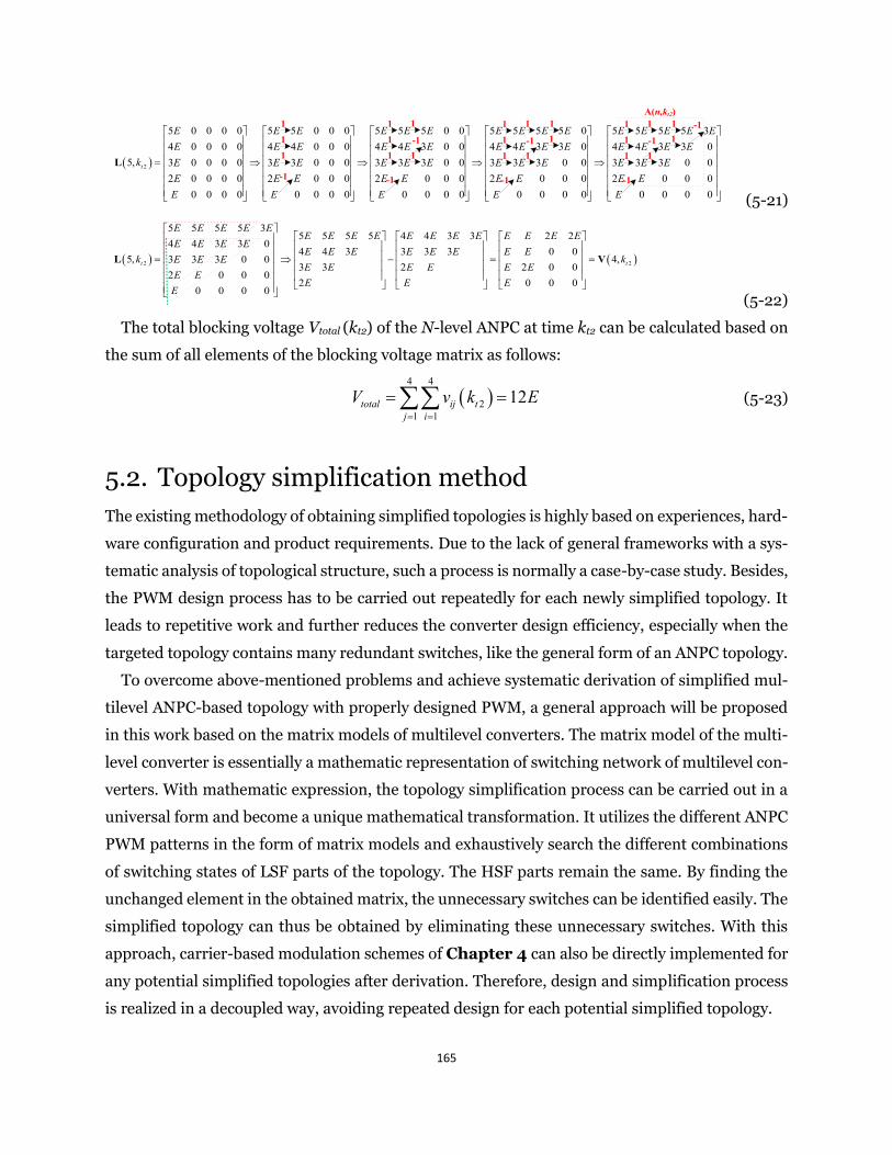
165
( )2
5 0 0 0 0 5 5 0 0 0 5 5 5 0 0 5 5 5 5 04 0 0 0 0 4 4 0 0 0 4 4 3 0 0 4 4 3 3 0
5, 3 0 0 0 0 3 3 0 0 0 3 3 3 0 0 3 3 3 0 02 0 0 0 0 2 0 0 0 2 0 0 0 2 0 0 0
0 0 0 0 0 0 0 0 0 0 0 0 0 0 0 0
t
E E E E E E E E E EE E E E E E E E E E
k E E E E E E E E EE E E E E E E
E E E E
=
L
5 5 5 5 34 4 3 3 03 3 3 0 02 0 0 0
0 0 0 0
E E E E EE E E EE E EE E
E
1
1
1
-1
1
1
1
-1
1
-11
1
1
1
-1
1
-11
11
1
1
1
-1
1
-11
11
-1A(n,kt2)
(5-21)
( ) ( )2 2
5 5 5 5 35 5 5 5 4 4 3 3 2 2
4 4 3 3 04 4 3 3 3 3 0 0
5, 4,3 3 3 0 03 3 2 2 0 0
2 0 0 02 0 0 0
0 0 0 0
t t
E E E E EE E E E E E E E E E E E
E E E EE E E E E E E E
k kE E EE E E E E E
E EE E E
E
= − = =
L V
(5-22)
The total blocking voltage Vtotal (kt2) of the N-level ANPC at time kt2 can be calculated based on
the sum of all elements of the blocking voltage matrix as follows:
( )4 4
21 1
12ij tj i
total v k EV= =
= = (5-23)
5.2. Topology simplification method
The existing methodology of obtaining simplified topologies is highly based on experiences, hard-
ware configuration and product requirements. Due to the lack of general frameworks with a sys-
tematic analysis of topological structure, such a process is normally a case-by-case study. Besides,
the PWM design process has to be carried out repeatedly for each newly simplified topology. It
leads to repetitive work and further reduces the converter design efficiency, especially when the
targeted topology contains many redundant switches, like the general form of an ANPC topology.
To overcome above-mentioned problems and achieve systematic derivation of simplified mul-
tilevel ANPC-based topology with properly designed PWM, a general approach will be proposed
in this work based on the matrix models of multilevel converters. The matrix model of the multi-
level converter is essentially a mathematic representation of switching network of multilevel con-
verters. With mathematic expression, the topology simplification process can be carried out in a
universal form and become a unique mathematical transformation. It utilizes the different ANPC
PWM patterns in the form of matrix models and exhaustively search the different combinations
of switching states of LSF parts of the topology. The HSF parts remain the same. By finding the
unchanged element in the obtained matrix, the unnecessary switches can be identified easily. The
simplified topology can thus be obtained by eliminating these unnecessary switches. With this
approach, carrier-based modulation schemes of Chapter 4 can also be directly implemented for
any potential simplified topologies after derivation. Therefore, design and simplification process
is realized in a decoupled way, avoiding repeated design for each potential simplified topology.
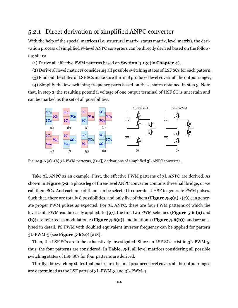
166
5.2.1 Direct derivation of simplified ANPC converter
With the help of the special matrices (i.e. structural matrix, status matrix, level matrix), the deri-
vation process of simplified N-level ANPC converters can be directly derived based on the follow-
ing steps:
(1) Derive all effective PWM patterns based on Section 4.1.3 (in Chapter 4),
(2) Derive all level matrices considering all possible switching states of LSF SCs for each pattern,
(3) Find out the states of LSF SCs make sure the final produced level covers all the output ranges,
(4) Simplify the low switching frequency parts based on these states obtained in step 3. Note
that, in step 2, the resulting potential voltage of one output terminal of HSF SC is uncertain and
can be marked as the set of all possibilities.
(i) (j)
3L-PWM-3 3L-PWM-4
SC12
SC21
SC12
SC21
SC11
SC12
SC21
SC12
SC21
SC11
SC12
SC21
SC12
SC21
SC11
SC12
SC21
SC12
SC21
SC11
SC12
SC21
SC12
SC21
SC11
SC12
SC21
SC12
SC21
SC11
SC12
SC21
SC12
SC21
SC11
SC12
SC21
SC12
SC21
SC11
(a)
(e)
(b)
(f)
(c)
(g)
(d)
(h)
Figure 5-6 (a)~(h) 3L PWM patterns, (i)~(j) derivations of simplified 3L ANPC converter.
Take 3L ANPC as an example. First, the effective PWM patterns of 3L ANPC are derived. As
shown in Figure 5-2, a phase leg of three-level ANPC converter contains three half bridge, or we
call them SCs. And each one of them can be selected to operate at HSF to generate PWM pulses.
Such that, there are totally 8 possibilities, and only five of them (Figure 5-3(a)~(e)) can gener-
ate proper PWM pulses as expected. For 3L ANPC, there are four PWM patterns of which the
level-shift PWM can be easily applied. In [97], the first two PWM schemes (Figure 5-6 (a) and
(b)) are referred as modulation 2 (Figure 5-6(a)), modulation 1 (Figure 5-6(b)), and are ana-
lyzed in detail. PS PWM with doubled equivalent inverter frequency can be applied for pattern
3L-PWM-5 (see Figure 5-6(e)) [218].
Then, the LSF SCs are to be exhaustively investigated. Since no LSF SCs exist in 3L-PWM-5,
thus, the four patterns are considered. In Table. 5-I, all level matrices considering all possible
switching states of LSF SCs for four patterns are derived.
Thirdly, the switching states that make sure the final produced level covers all the output ranges
are determined as the LSF parts of 3L-PWM-3 and 3L-PWM-4.
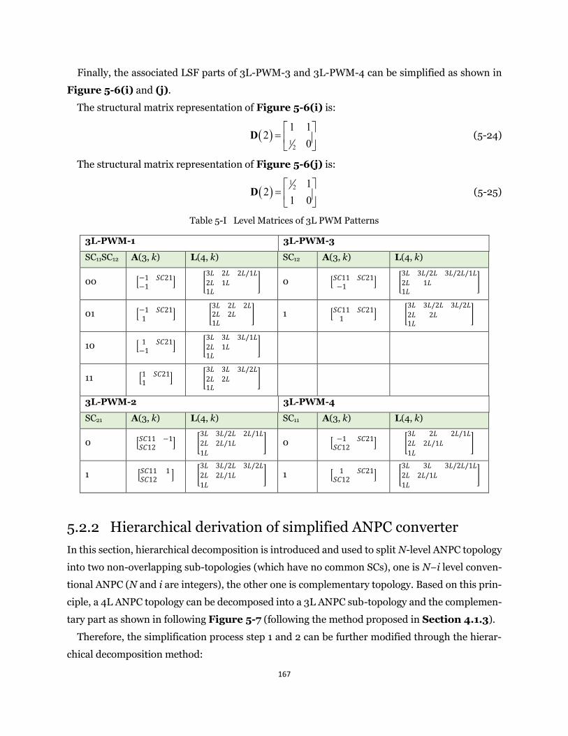
167
Finally, the associated LSF parts of 3L-PWM-3 and 3L-PWM-4 can be simplified as shown in
Figure 5-6(i) and (j).
The structural matrix representation of Figure 5-6(i) is:
( )1
2
1 12
0
=
D (5-24)
The structural matrix representation of Figure 5-6(j) is:
( )1
2 12
1 0
=
D (5-25)
Table 5-I Level Matrices of 3L PWM Patterns
3L-PWM-1 3L-PWM-3
SC11SC12 A(3, k) L(4, k) SC12 A(3, k) L(4, k)
00 [−1 𝑆𝐶21−1
] [3𝐿 2𝐿 2𝐿/1𝐿
2𝐿 1𝐿1𝐿
] 0 [𝑆𝐶11 𝑆𝐶21
−1] [
3𝐿 3𝐿/2𝐿 3𝐿/2𝐿/1𝐿
2𝐿 1𝐿1𝐿
]
01 [−1 𝑆𝐶211
] [3𝐿 2𝐿 2𝐿2𝐿 2𝐿1𝐿
] 1 [𝑆𝐶11 𝑆𝐶21
1] [
3𝐿 3𝐿/2𝐿 3𝐿/2𝐿
2𝐿 2𝐿1𝐿
]
10 [1 𝑆𝐶21
−1] [
3𝐿 3𝐿 3𝐿/1𝐿
2𝐿 1𝐿1𝐿
]
11 [1 𝑆𝐶211
] [3𝐿 3𝐿 3𝐿/2𝐿
2𝐿 2𝐿1𝐿
]
3L-PWM-2 3L-PWM-4
SC21 A(3, k) L(4, k) SC11 A(3, k) L(4, k)
0 [𝑆𝐶11 −1𝑆𝐶12
] [3𝐿 3𝐿/2𝐿 2𝐿/1𝐿
2𝐿 2𝐿/1𝐿
1𝐿
] 0 [−1 𝑆𝐶21
𝑆𝐶12] [
3𝐿 2𝐿 2𝐿/1𝐿
2𝐿 2𝐿/1𝐿
1𝐿
]
1 [𝑆𝐶11 1𝑆𝐶12
] [3𝐿 3𝐿/2𝐿 3𝐿/2𝐿
2𝐿 2𝐿/1𝐿
1𝐿
] 1 [1 𝑆𝐶21
𝑆𝐶12] [
3𝐿 3𝐿 3𝐿/2𝐿/1𝐿
2𝐿 2𝐿/1𝐿
1𝐿
]
5.2.2 Hierarchical derivation of simplified ANPC converter
In this section, hierarchical decomposition is introduced and used to split N-level ANPC topology
into two non-overlapping sub-topologies (which have no common SCs), one is N−i level conven-
tional ANPC (N and i are integers), the other one is complementary topology. Based on this prin-
ciple, a 4L ANPC topology can be decomposed into a 3L ANPC sub-topology and the complemen-
tary part as shown in following Figure 5-7 (following the method proposed in Section 4.1.3).
Therefore, the simplification process step 1 and 2 can be further modified through the hierar-
chical decomposition method:
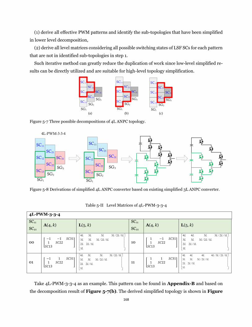
168
(1) derive all effective PWM patterns and identify the sub-topologies that have been simplified
in lower level decomposition,
(2) derive all level matrices considering all possible switching states of LSF SCs for each pattern
that are not in identified sub-topologies in step 1.
Such iterative method can greatly reduce the duplication of work since low-level simplified re-
sults can be directly utilized and are suitable for high-level topology simplification.
SC12
SC22
SC13
SC21
SC31SC12
SC13
SC22
SG1
SG2
SC11SC11
SC21
SC31
SG3
SC12
SC22
SC13
SC21
SC31SC12
SC13
SC22
SG1
SG2
SC11SC11
SC21
SC31
SG3
SC12
SC22
SC13
SC21
SC31SC12
SC13
SC22
SG1
SG2
SC11SC11
SC21
SC31
SG3
(a) (b) (c) Figure 5-7 Three possible decompositions of 4L ANPC topology.
SG1
SG2
SG3
SC11
SC13
SC31
4L-PWM-3-3-4
SG1
SG2
SG3
SC13
SC11
SC21
SC31SC12
SC21
SC22 SC22
SC12
Figure 5-8 Derivations of simplified 4L ANPC converter based on existing simplified 3L ANPC converter.
Table 5-II Level Matrices of 4L-PWM-3-3-4
4L-PWM-3-3-4
SC11
SC21 A(4, k) L(5, k)
SC11
SC21 A(4, k) L(5, k)
00 [−1 −1 𝑆𝐶311 𝑆𝐶22
𝑆𝐶13]
4 3 3 3 / 2 /13 3 3 / 2 /12 2 /11
L L L L L LL L L L LL L LL
10 [1 −1 𝑆𝐶311 𝑆𝐶22
𝑆𝐶13]
4 4 3 3 / 2 /13 3 3 / 2 /12 2 /11
L L L L L LL L L L LL L LL
01 [−1 1 𝑆𝐶311 𝑆𝐶22
𝑆𝐶13]
4 3 3 3 / 2 /13 3 3 / 2 /12 2 /11
L L L L L LL L L L LL L LL
11 [1 1 𝑆𝐶311 𝑆𝐶22
𝑆𝐶13]
4 4 4 4 / 3 / 2 / 13 3 3 / 2 / 12 2 / 11
L L L L L L LL L L L LL L LL
Take 4L-PWM-3-3-4 as an example. This pattern can be found in Appendix-B and based on
the decomposition result of Figure 5-7(b). The derived simplified topology is shown in Figure
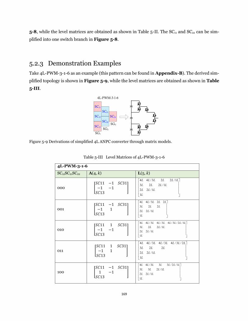
169
5-8, while the level matrices are obtained as shown in Table 5-II. The SC11 and SC21 can be sim-
plified into one switch branch in Figure 5-8.
5.2.3 Demonstration Examples
Take 4L-PWM-3-1-6 as an example (this pattern can be found in Appendix-B). The derived sim-
plified topology is shown in Figure 5-9, while the level matrices are obtained as shown in Table
5-III.
SC12
SC22
SC21
SG1
SG2
SG3
SC11
SC13
SC31
4L-PWM-3-1-6
Figure 5-9 Derivations of simplified 4L ANPC converter through matrix models.
Table 5-III Level Matrices of 4L-PWM-3-1-6
4L-PWM-3-1-6
SC12SC21SC22 A(4, k) L(5, k)
000 [𝑆𝐶11 −1 𝑆𝐶31
−1 −1𝑆𝐶13
]
4 4 / 3 2 2 /13 2 2 /12 2 /11
L L L L L LL L L LL L LL
001 [𝑆𝐶11 −1 𝑆𝐶31
−1 1𝑆𝐶13
]
4 4 / 3 2 23 2 22 2 /11
L L L L LL L LL L LL
010 [𝑆𝐶11 1 𝑆𝐶31
−1 −1𝑆𝐶13
]
4 4 / 3 4 / 3 4 / 3 / 2 /13 2 2 /12 2 /11
L L L L L L L L LL L L LL L LL
011 [𝑆𝐶11 1 𝑆𝐶31
−1 1𝑆𝐶13
]
4 4 / 3 4 / 3 4 / 3 / 23 2 22 2 /11
L L L L L L L LL L LL L LL
100 [𝑆𝐶11 −1 𝑆𝐶31
1 −1𝑆𝐶13
]
4 4 / 3 3 3 / 2 /13 3 2 /12 2 /11
L L L L L L LL L L LL L LL
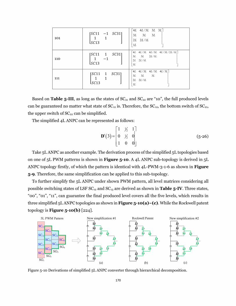
170
101 [𝑆𝐶11 −1 𝑆𝐶31
1 1𝑆𝐶13
]
4 4 / 3 3 33 3 32 2 /11
L L L L LL L LL L LL
110 [𝑆𝐶11 1 𝑆𝐶31
1 −1𝑆𝐶13
]
4 4 / 3 4 / 3 4 / 3 / 2 /13 3 2 /12 2 /11
L L L L L L L L LL L L LL L LL
111 [𝑆𝐶11 1 𝑆𝐶31
1 1𝑆𝐶13
]
4 4 / 3 4 / 3 4 / 33 3 32 2 /11
L L L L L L LL L LL L LL
Based on Table 5-III, as long as the states of SC21 and SC22 are “10”, the full produced levels
can be guaranteed no matter what state of SC12 is. Therefore, the SC12, the bottom switch of SC21,
the upper switch of SC22 can be simplified.
The simplified 4L ANPC can be represented as follows:
( )
12
12
1 13 0 0
1 0 0
=
D (5-26)
Take 5L ANPC as another example. The derivation process of the simplified 5L topologies based
on one of 5L PWM patterns is shown in Figure 5-10. A 4L ANPC sub-topology is derived in 5L
ANPC topology firstly, of which the pattern is identical with 4L-PWM-3-1-6 as shown in Figure
5-9. Therefore, the same simplification can be applied to this sub-topology.
To further simplify the 5L ANPC under shown PWM pattern, all level matrices considering all
possible switching states of LSF SC12 and SC13 are derived as shown in Table 5-IV. Three states,
“00”, “01”, “11”, can guarantee the final produced level covers all the five levels, which results in
three simplified 5L ANPC topologies as shown in Figure 5-10(a)~(c). While the Rockwell patent
topology is Figure 5-10(b) [224].
Rockwell Patent
SC32
SC41
SC23
SC14
SC11
SC12
SC22
SC13
SC21
SC31
SG1
SG2
SG3
SG4
5L PWM Pattern New simplification #1 New simplification #2
(a) (b) (c) Figure 5-10 Derivations of simplified 5L ANPC converter through hierarchical decomposition.
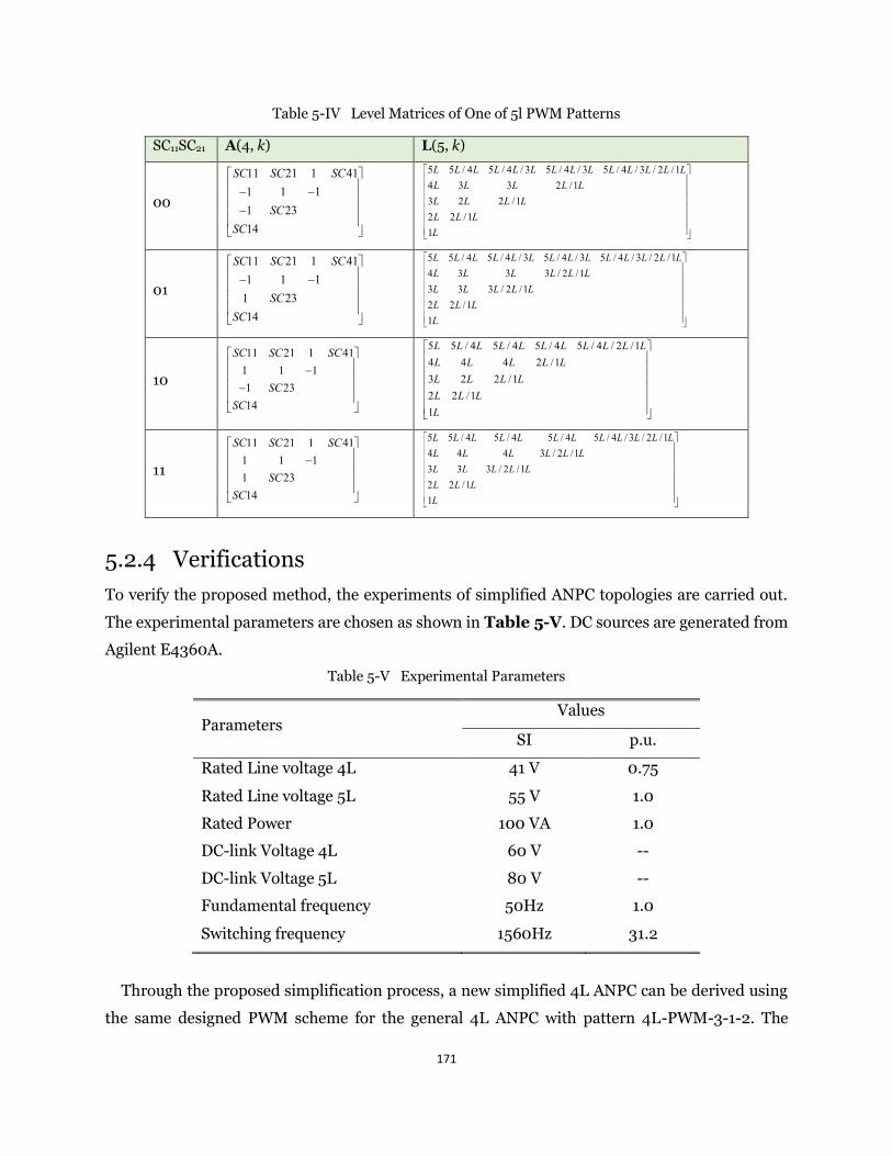
171
Table 5-IV Level Matrices of One of 5l PWM Patterns
SC11SC21 A(4, k) L(5, k)
00
11 21 1 411 1 11 2314
SC SC SC
SCSC
− −
−
5 5 / 4 5 / 4 / 3 5 / 4 / 3 5 / 4 / 3 / 2 /14 3 3 2 /13 2 2 /12 2 /11
L L L L L L L L L L L L L LL L L L LL L L LL L LL
01
11 21 1 411 1 1
1 2314
SC SC SC
SCSC
− −
5 5 / 4 5 / 4 / 3 5 / 4 / 3 5 / 4 / 3 / 2 /14 3 3 3 / 2 /13 3 3 / 2 /12 2 /11
L L L L L L L L L L L L L LL L L L L LL L L L LL L LL
10
11 21 1 411 1 11 2314
SC SC SC
SCSC
− −
5 5 / 4 5 / 4 5 / 4 5 / 4 / 2 /14 4 4 2 /13 2 2 /12 2 /11
L L L L L L L L L L LL L L L LL L L LL L LL
11
11 21 1 411 1 11 2314
SC SC SC
SCSC
−
5 5 / 4 5 / 4 5 / 4 5 / 4 / 3 / 2 /14 4 4 3 / 2 /13 3 3 / 2 /12 2 /11
L L L L L L L L L L L LL L L L L LL L L L LL L LL
5.2.4 Verifications
To verify the proposed method, the experiments of simplified ANPC topologies are carried out.
The experimental parameters are chosen as shown in Table 5-V. DC sources are generated from
Agilent E4360A.
Table 5-V Experimental Parameters
Parameters Values
SI p.u.
Rated Line voltage 4L 41 V 0.75
Rated Line voltage 5L 55 V 1.0
Rated Power 100 VA 1.0
DC-link Voltage 4L 60 V --
DC-link Voltage 5L 80 V --
Fundamental frequency 50Hz 1.0
Switching frequency 1560Hz 31.2
Through the proposed simplification process, a new simplified 4L ANPC can be derived using
the same designed PWM scheme for the general 4L ANPC with pattern 4L-PWM-3-1-2. The
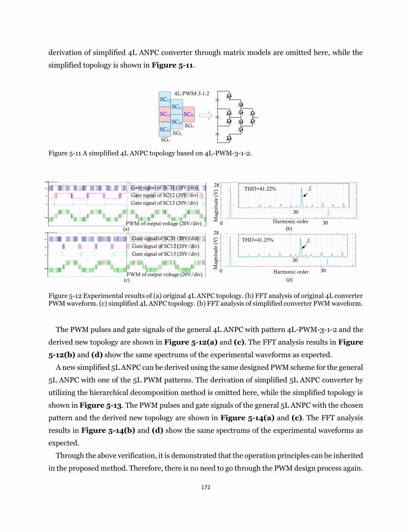
172
derivation of simplified 4L ANPC converter through matrix models are omitted here, while the
simplified topology is shown in Figure 5-11.
SC12
SC22
SC21
SG1
SG2
SG3
SC11
SC13
SC31
4L-PWM-3-1-2
Figure 5-11 A simplified 4L ANPC topology based on 4L-PWM-3-1-2.
fsTHD=41.25%
THD=41.22% fs
(c)
(a)
(d)
(b)
Gate signal of SC31 (20V/div)
Gate signal of SC12 (20V/div)
Gate signal of SC13 (20V/div)
PWM of output voltage (20V/div) Harmonic order
Harmonic order
Mag
nitu
de (
V)
Gate signal of SC31 (20V/div)
Gate signal of SC12 (20V/div)
Gate signal of SC13 (20V/div)
PWM of output voltage (20V/div)
0
28
30
30M
agni
tude
(V
)
0
28
30
30
Figure 5-12 Experimental results of (a) original 4L ANPC topology. (b) FFT analysis of original 4L converter PWM waveform. (c) simplified 4L ANPC topology. (b) FFT analysis of simplified converter PWM waveform.
The PWM pulses and gate signals of the general 4L ANPC with pattern 4L-PWM-3-1-2 and the
derived new topology are shown in Figure 5-12(a) and (c). The FFT analysis results in Figure
5-12(b) and (d) show the same spectrums of the experimental waveforms as expected.
A new simplified 5L ANPC can be derived using the same designed PWM scheme for the general
5L ANPC with one of the 5L PWM patterns. The derivation of simplified 5L ANPC converter by
utilizing the hierarchical decomposition method is omitted here, while the simplified topology is
shown in Figure 5-13. The PWM pulses and gate signals of the general 5L ANPC with the chosen
pattern and the derived new topology are shown in Figure 5-14(a) and (c). The FFT analysis
results in Figure 5-14(b) and (d) show the same spectrums of the experimental waveforms as
expected.
Through the above verification, it is demonstrated that the operation principles can be inherited
in the proposed method. Therefore, there is no need to go through the PWM design process again.
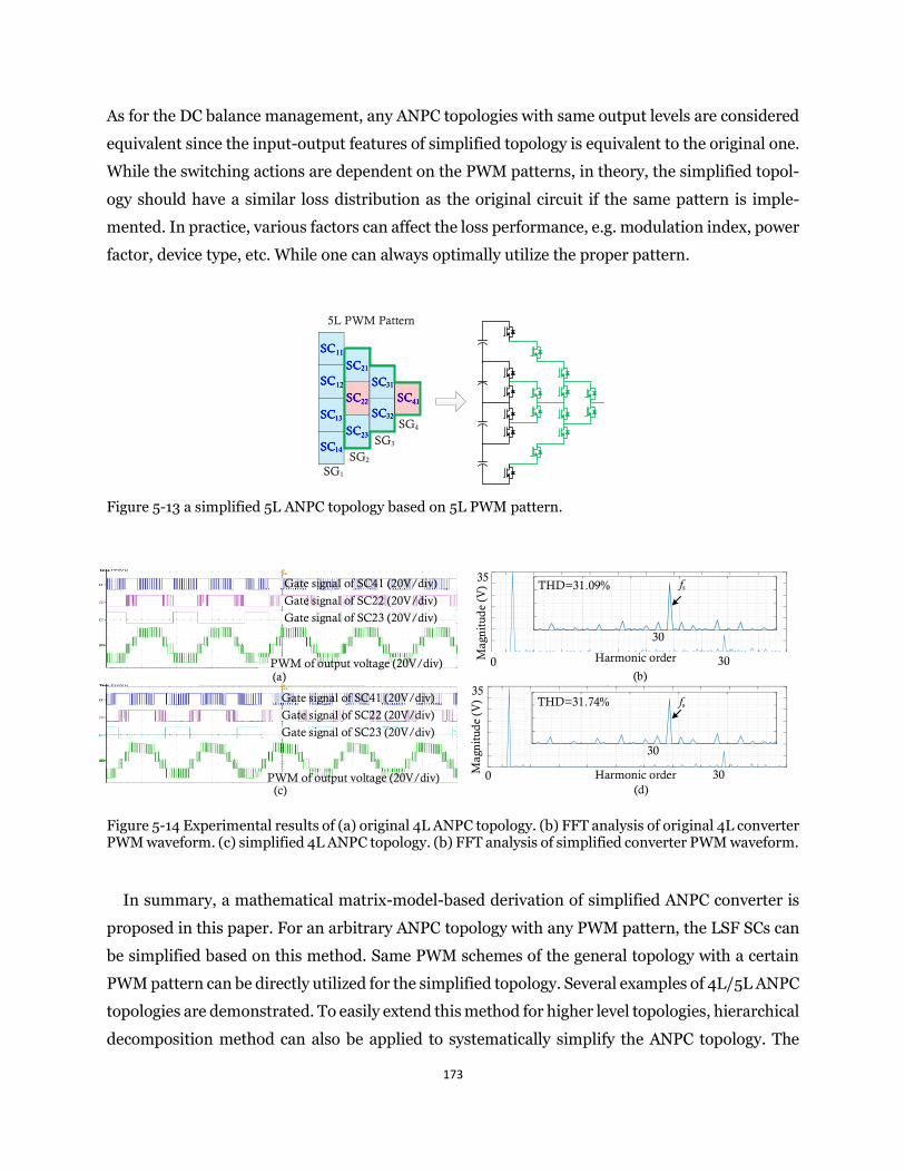
173
As for the DC balance management, any ANPC topologies with same output levels are considered
equivalent since the input-output features of simplified topology is equivalent to the original one.
While the switching actions are dependent on the PWM patterns, in theory, the simplified topol-
ogy should have a similar loss distribution as the original circuit if the same pattern is imple-
mented. In practice, various factors can affect the loss performance, e.g. modulation index, power
factor, device type, etc. While one can always optimally utilize the proper pattern.
SC32
SC41
SC23
SC14
SC11
SC12
SC22
SC13
SC21
SC31SC12
SC13
SC22
SG1
SG2
SC11
SC21
SC31
SG3SC14
SC23
SC32
SC41
SG4
5L PWM Pattern
Figure 5-13 a simplified 5L ANPC topology based on 5L PWM pattern.
THD=31.74% fs
THD=31.09% fs
(c)
(a)
(d)
(b)
Gate signal of SC41 (20V/div)
Gate signal of SC22 (20V/div)
Gate signal of SC23 (20V/div)
PWM of output voltage (20V/div)
Gate signal of SC41 (20V/div)
Gate signal of SC22 (20V/div)
Gate signal of SC23 (20V/div)
PWM of output voltage (20V/div)
Mag
nitu
de (
V)
0
35
30
30
Mag
nitu
de (
V)
0
35
30
30
Harmonic order
Harmonic order
Figure 5-14 Experimental results of (a) original 4L ANPC topology. (b) FFT analysis of original 4L converter PWM waveform. (c) simplified 4L ANPC topology. (b) FFT analysis of simplified converter PWM waveform.
In summary, a mathematical matrix-model-based derivation of simplified ANPC converter is
proposed in this paper. For an arbitrary ANPC topology with any PWM pattern, the LSF SCs can
be simplified based on this method. Same PWM schemes of the general topology with a certain
PWM pattern can be directly utilized for the simplified topology. Several examples of 4L/5L ANPC
topologies are demonstrated. To easily extend this method for higher level topologies, hierarchical
decomposition method can also be applied to systematically simplify the ANPC topology. The
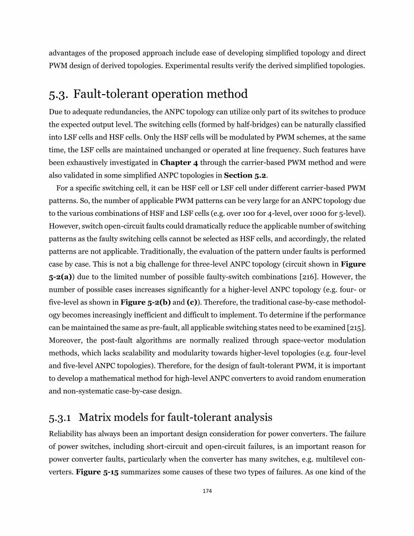
174
advantages of the proposed approach include ease of developing simplified topology and direct
PWM design of derived topologies. Experimental results verify the derived simplified topologies.
5.3. Fault-tolerant operation method
Due to adequate redundancies, the ANPC topology can utilize only part of its switches to produce
the expected output level. The switching cells (formed by half-bridges) can be naturally classified
into LSF cells and HSF cells. Only the HSF cells will be modulated by PWM schemes, at the same
time, the LSF cells are maintained unchanged or operated at line frequency. Such features have
been exhaustively investigated in Chapter 4 through the carrier-based PWM method and were
also validated in some simplified ANPC topologies in Section 5.2.
For a specific switching cell, it can be HSF cell or LSF cell under different carrier-based PWM
patterns. So, the number of applicable PWM patterns can be very large for an ANPC topology due
to the various combinations of HSF and LSF cells (e.g. over 100 for 4-level, over 1000 for 5-level).
However, switch open-circuit faults could dramatically reduce the applicable number of switching
patterns as the faulty switching cells cannot be selected as HSF cells, and accordingly, the related
patterns are not applicable. Traditionally, the evaluation of the pattern under faults is performed
case by case. This is not a big challenge for three-level ANPC topology (circuit shown in Figure
5-2(a)) due to the limited number of possible faulty-switch combinations [216]. However, the
number of possible cases increases significantly for a higher-level ANPC topology (e.g. four- or
five-level as shown in Figure 5-2(b) and (c)). Therefore, the traditional case-by-case methodol-
ogy becomes increasingly inefficient and difficult to implement. To determine if the performance
can be maintained the same as pre-fault, all applicable switching states need to be examined [215].
Moreover, the post-fault algorithms are normally realized through space-vector modulation
methods, which lacks scalability and modularity towards higher-level topologies (e.g. four-level
and five-level ANPC topologies). Therefore, for the design of fault-tolerant PWM, it is important
to develop a mathematical method for high-level ANPC converters to avoid random enumeration
and non-systematic case-by-case design.
5.3.1 Matrix models for fault-tolerant analysis
Reliability has always been an important design consideration for power converters. The failure
of power switches, including short-circuit and open-circuit failures, is an important reason for
power converter faults, particularly when the converter has many switches, e.g. multilevel con-
verters. Figure 5-15 summarizes some causes of these two types of failures. As one kind of the
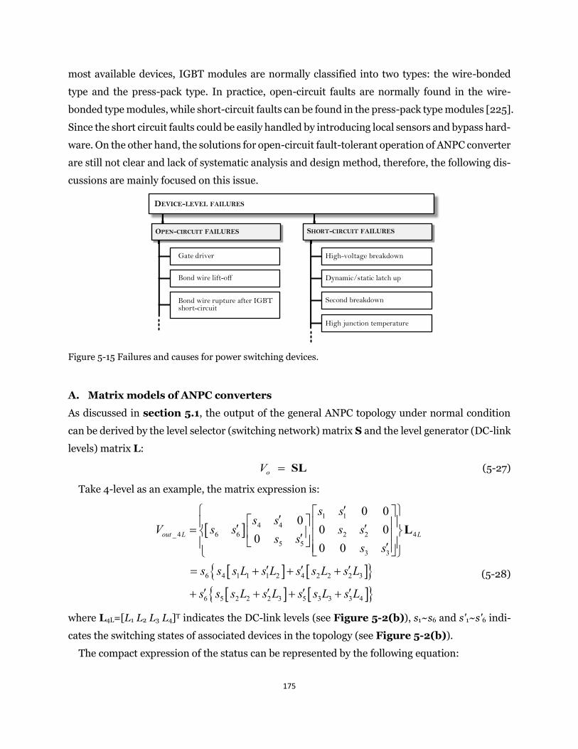
175
most available devices, IGBT modules are normally classified into two types: the wire-bonded
type and the press-pack type. In practice, open-circuit faults are normally found in the wire-
bonded type modules, while short-circuit faults can be found in the press-pack type modules [225].
Since the short circuit faults could be easily handled by introducing local sensors and bypass hard-
ware. On the other hand, the solutions for open-circuit fault-tolerant operation of ANPC converter
are still not clear and lack of systematic analysis and design method, therefore, the following dis-
cussions are mainly focused on this issue.
High-voltage breakdown
Dynamic/static latch up
Second breakdown
SHORT-CIRCUIT FAILURES
DEVICE-LEVEL FAILURES
OPEN-CIRCUIT FAILURES
Gate driver
Bond wire lift-off
Bond wire rupture after IGBT short-circuit
High junction temperature
Figure 5-15 Failures and causes for power switching devices.
A. Matrix models of ANPC converters
As discussed in section 5.1, the output of the general ANPC topology under normal condition
can be derived by the level selector (switching network) matrix S and the level generator (DC-link
levels) matrix L:
oV = SL (5-27)
Take 4-level as an example, the matrix expression is:
1 14 4
_ 4 6 6 2 2 45 5
3 3
6 4 1 1 1 2 4 2 2 2 3
6 5 2 2 2 3 5 3 3 3 4
0 00
0 00
0 0
out L L
s ss s
V s s s ss s
s s
s s s L s L s s L s L
s s s L s L s s L s L
=
= + + +
+ + + +
L
(5-28)
where L4L=[L1 L2 L3 L4]T indicates the DC-link levels (see Figure 5-2(b)), s1~s6 and s'1~s'6 indi-
cates the switching states of associated devices in the topology (see Figure 5-2(b)).
The compact expression of the status can be represented by the following equation:
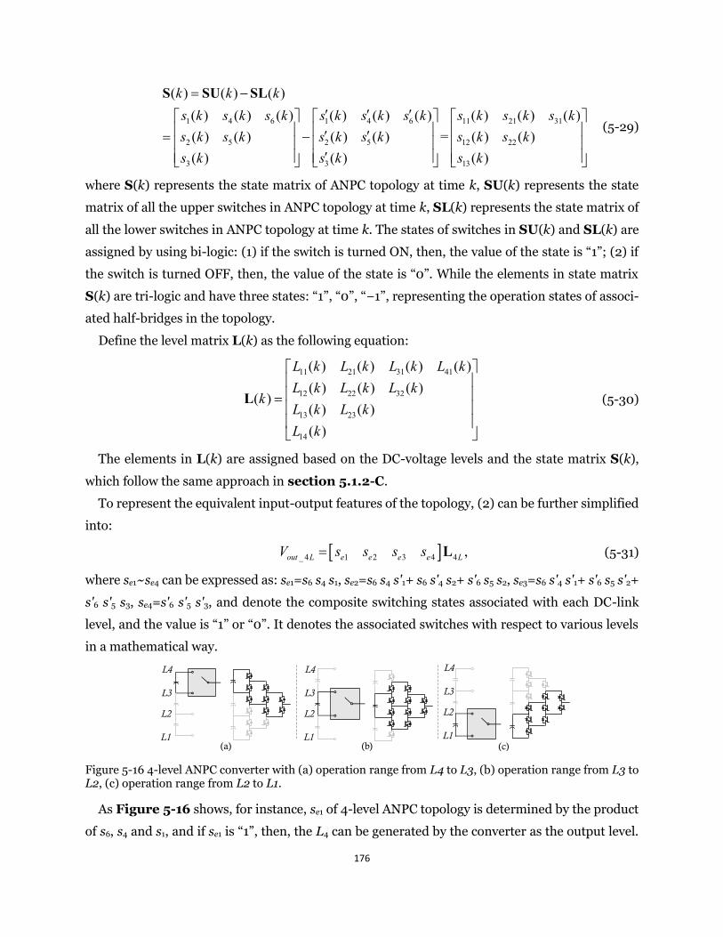
176
1 4 6 1 4 6 11 21 31
2 5 2 5 12 22
3 3 13
( ) ( ) ( )( ) ( ) ( ) ( ) ( ) ( ) ( ) ( ) ( )( ) ( ) ( ) ( ) = ( ) ( )( ) ( ) ( )
k k ks k s k s k s k s k s k s k s k s ks k s k s k s k s k s ks k s k s k
= −
= −
S SU SL
(5-29)
where S(k) represents the state matrix of ANPC topology at time k, SU(k) represents the state
matrix of all the upper switches in ANPC topology at time k, SL(k) represents the state matrix of
all the lower switches in ANPC topology at time k. The states of switches in SU(k) and SL(k) are
assigned by using bi-logic: (1) if the switch is turned ON, then, the value of the state is “1”; (2) if
the switch is turned OFF, then, the value of the state is “0”. While the elements in state matrix
S(k) are tri-logic and have three states: “1”, “0”, “−1”, representing the operation states of associ-
ated half-bridges in the topology.
Define the level matrix L(k) as the following equation:
11 21 31 41
12 22 32
13 23
14
( ) ( ) ( ) ( )( ) ( ) ( )
( )( ) ( )( )
L k L k L k L kL k L k L k
kL k L kL k
=
L (5-30)
The elements in L(k) are assigned based on the DC-voltage levels and the state matrix S(k),
which follow the same approach in section 5.1.2-C.
To represent the equivalent input-output features of the topology, (2) can be further simplified
into:
_ 4 1 2 3 4 4 ,out L e e e e LV s s s s= L (5-31)
where se1~se4 can be expressed as: se1=s6 s4 s1, se2=s6 s4 s'1+ s6 s'4 s2+ s'6 s5 s2, se3=s6 s'4 s'1+ s'6 s5 s'2+
s'6 s'5 s3, se4=s'6 s'5 s'3, and denote the composite switching states associated with each DC-link
level, and the value is “1” or “0”. It denotes the associated switches with respect to various levels
in a mathematical way.
L4
L3
L2
L1
L4
L3
L2
L1
L4
L3
L2
L1(a) (b) (c)
Figure 5-16 4-level ANPC converter with (a) operation range from L4 to L3, (b) operation range from L3 to L2, (c) operation range from L2 to L1.
As Figure 5-16 shows, for instance, se1 of 4-level ANPC topology is determined by the product
of s6, s4 and s1, and if se1 is “1”, then, the L4 can be generated by the converter as the output level.
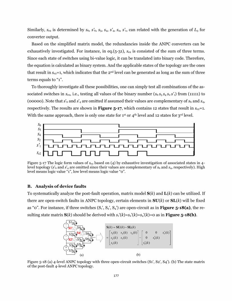
177
Similarly, se2 is determined by s6, s'6, s5, s4, s'4, s2, s'1, can related with the generation of L3 for
converter output.
Based on the simplified matrix model, the redundancies inside the ANPC converters can be
exhaustively investigated. For instance, in eq.(5-31), se2 is consisted of the sum of three terms.
Since each state of switches using bi-value logic, it can be translated into binary code. Therefore,
the equation is calculated as binary system. And the applicable states of the topology are the ones
that result in se2=1, which indicates that the 2nd level can be generated as long as the sum of three
terms equals to “1”.
To thoroughly investigate all these possibilities, one can simply test all combinations of the as-
sociated switches in se2, i.e., testing all values of the binary number (s6 s5 s4 s2 s'1) from (11111) to
(00000). Note that s'6 and s'4 are omitted if assumed their values are complementary of s6 and s4,
respectively. The results are shown in Figure 5-17, which contains 12 states that result in se2=1.
With the same approach, there is only one state for 1st or 4th level and 12 states for 3rd level.
s6s5
s4
s2
s'1
se2
Figure 5-17 The logic form values of se2 based on (4) by exhaustive investigation of associated states in 4-level topology (s'6 and s'4 are omitted since their values are complementary of s6 and s4, respectively). High level means logic value “1”, low level means logic value “0”.
B. Analysis of device faults
To systematically analyze the post-fault operation, matrix model S(k) and L(k) can be utilized. If
there are open-switch faults in ANPC topology, certain elements in SU(k) or SL(k) will be fixed
as “0”. For instance, if three switches (S1', S2', S4') are open-circuit as in Figure 5-18(a), the re-
sulting state matrix S(k) should be derived with s1'(k)=s2'(k)=s4'(k)=0 as in Figure 5-18(b).
S1
S1'
S2
S2'
S3
S3'
S4
S4'
S5
S5'
S6
S6'
(a) (b)
Figure 5-18 (a) 4-level ANPC topology with three open-circuit switches (S1', S2', S4'). (b) The state matrix of the post-fault 4-level ANPC topology.
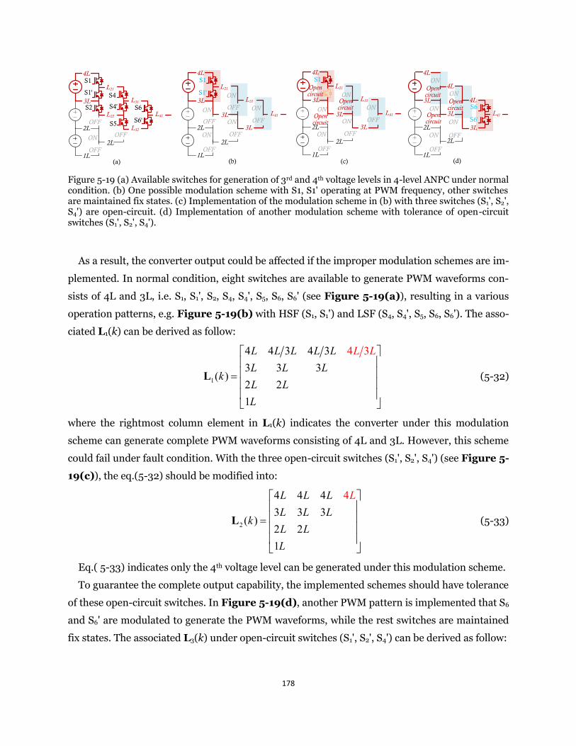
178
4L
3L
2L
1L(d)
ON
ON
OFF
ON
OFF
ON
S6
S6'
ON
(a) (c)
S1
S1'
S2
S4
S4'
S5
S6
S6'
OFF
ON
OFF
OFF
L21
L22
2L
L31
L32
L41
4L
3L
2L
1L
4L
3L
2L
4L
3L
L41
4L
3L
2L
1L(b)
S1
S1'
OFF
ON
OFF
OFF
L21
2L
L31
L41
OFF
OFFON3L
3LON
ON
ON
4L
3L
2L
1L
S1Open circuit
OFF
ON
OFF
L21
2L
L31
L41
OFFON3L
3LON
ON
ON
Open circuit
Open circuit
Open circuit
Open circuit
Open circuit
Figure 5-19 (a) Available switches for generation of 3rd and 4th voltage levels in 4-level ANPC under normal condition. (b) One possible modulation scheme with S1, S1' operating at PWM frequency, other switches are maintained fix states. (c) Implementation of the modulation scheme in (b) with three switches (S1', S2', S4') are open-circuit. (d) Implementation of another modulation scheme with tolerance of open-circuit switches (S1', S2', S4').
As a result, the converter output could be affected if the improper modulation schemes are im-
plemented. In normal condition, eight switches are available to generate PWM waveforms con-
sists of 4L and 3L, i.e. S1, S1', S2, S4, S4', S5, S6, S6' (see Figure 5-19(a)), resulting in a various
operation patterns, e.g. Figure 5-19(b) with HSF (S1, S1') and LSF (S4, S4', S5, S6, S6'). The asso-
ciated L1(k) can be derived as follow:
1
4 4 3 4 33 3
43
( )2 21
3L
L
LL LL L LL L L
kLL
=
L (5-32)
where the rightmost column element in L1(k) indicates the converter under this modulation
scheme can generate complete PWM waveforms consisting of 4L and 3L. However, this scheme
could fail under fault condition. With the three open-circuit switches (S1', S2', S4') (see Figure 5-
19(c)), the eq.(5-32) should be modified into:
2
4 4 43 3 3
( )2 21
4L L LL L L
k
L
L LL
=
L (5-33)
Eq.( 5-33) indicates only the 4th voltage level can be generated under this modulation scheme.
To guarantee the complete output capability, the implemented schemes should have tolerance
of these open-circuit switches. In Figure 5-19(d), another PWM pattern is implemented that S6
and S6' are modulated to generate the PWM waveforms, while the rest switches are maintained
fix states. The associated L3(k) under open-circuit switches (S1', S2', S4') can be derived as follow:
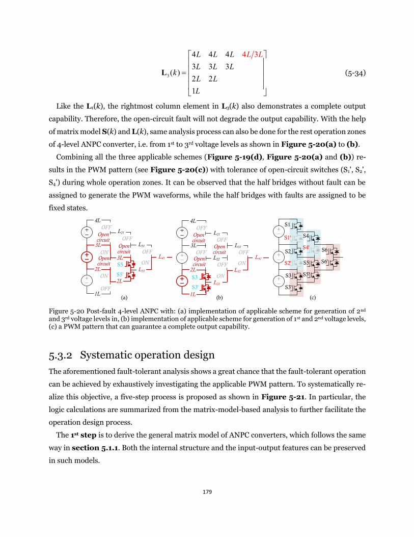
179
3
4 4 43 3 3
)2 21
4 3
(
L L L LLL L L
kL LL
=
L (5-34)
Like the L1(k), the rightmost column element in L3(k) also demonstrates a complete output
capability. Therefore, the open-circuit fault will not degrade the output capability. With the help
of matrix model S(k) and L(k), same analysis process can also be done for the rest operation zones
of 4-level ANPC converter, i.e. from 1st to 3rd voltage levels as shown in Figure 5-20(a) to (b).
Combining all the three applicable schemes (Figure 5-19(d), Figure 5-20(a) and (b)) re-
sults in the PWM pattern (see Figure 5-20(c)) with tolerance of open-circuit switches (S1', S2',
S4') during whole operation zones. It can be observed that the half bridges without fault can be
assigned to generate the PWM waveforms, while the half bridges with faults are assigned to be
fixed states.
S1
S1'
S2
S2'
S3
S3'
S4
S4'
S5
S5'
S6
S6'
(a)
ON
OFF
ON
4L
3L
2L
1L
3L
2L
L41
Open circuit
Open circuit
Open circuit
S5
S5'L32
ON
OFF
(b)
4L
3L
2L
1L
L41
Open circuit
Open circuit
Open circuit
L32
ON
OFF
(c)
S3
S3'
ON
OFF
L23
OFF
OFF
OFFOFF
OFF
L21
L22
L31
L21
L31
Figure 5-20 Post-fault 4-level ANPC with: (a) implementation of applicable scheme for generation of 2nd and 3rd voltage levels in, (b) implementation of applicable scheme for generation of 1st and 2nd voltage levels, (c) a PWM pattern that can guarantee a complete output capability.
5.3.2 Systematic operation design
The aforementioned fault-tolerant analysis shows a great chance that the fault-tolerant operation
can be achieved by exhaustively investigating the applicable PWM pattern. To systematically re-
alize this objective, a five-step process is proposed as shown in Figure 5-21. In particular, the
logic calculations are summarized from the matrix-model-based analysis to further facilitate the
operation design process.
The 1st step is to derive the general matrix model of ANPC converters, which follows the same
way in section 5.1.1. Both the internal structure and the input-output features can be preserved
in such models.
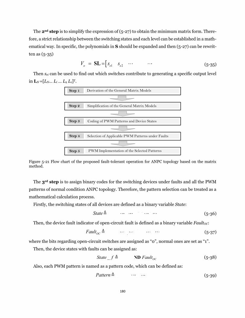
180
The 2nd step is to simplify the expression of (5-27) to obtain the minimum matrix form. There-
fore, a strict relationship between the switching states and each level can be established in a math-
ematical way. In specific, the polynomials in S should be expanded and then (5-27) can be rewrit-
ten as (5-35)
1 2 o e e ei NV s s s= =SL Lei NV s s s L (5-35)
Then sei can be used to find out which switches contribute to generating a specific output level
in LN =[LN… Li … L2 L1]T.
Derivation of the General Matrix ModelsStep 1
Step 2 Simplification of the General Matrix Models
Step 3
Step 4
Step 5
Selection of Applicable PWM Patterns under Faults
Coding of PWM Patterns and Device States
PWM Implementation of the Selected Patterns
Figure 5-21 Flow chart of the proposed fault-tolerant operation for ANPC topology based on the matrix method.
The 3rd step is to assign binary codes for the switching devices under faults and all the PWM
patterns of normal condition ANPC topology. Therefore, the pattern selection can be treated as a
mathematical calculation process.
Firstly, the switching states of all devices are defined as a binary variable State:
( )1 2 3 1 2 3i iState s s s s s s s s ( )1 2 3 i i1 2 3i i1 2 3State s s s s s s s s(State s s s s s s s s( 1 2 3State s s s s s s s s1 2 3 1 2 3State s s s s s s s s1 2 3i iState s s s s s s s si i1 2 3i i1 2 3State s s s s s s s s1 2 3i i1 2 3 State s s s s s s s s State s s s s s s s s (5-36)
Then, the device fault indicator of open-circuit fault is defined as a binary variable FaultOC:
( )1 2 3 1 2 3OC i iFault f f f f f f f f ( )1 2 3 1 2 3i iFault f f f f f f f f(Fault f f f f f f f f( 1 2 3Fault f f f f f f f f1 2 3 1 2 3Fault f f f f f f f f1 2 3iFault f f f f f f f fi iFault f f f f f f f fi Fault f f f f f f f f Fault f f f f f f f f (5-37)
where the bits regarding open-circuit switches are assigned as “0”, normal ones are set as “1”.
Then, the device states with faults can be assigned as:
_ OCState f State FaultANDState f State Fault_ State f State Fault_ State f State FaultANDState f State Fault_ State f State Fault_ AND_ State f State Fault_ (5-38)
Also, each PWM pattern is named as a pattern code, which can be defined as:
( )1 2 3 iPattern p p p p( )1 2 3 iPattern p p p p(Pattern p p p p( 1 2 3Pattern p p p p1 2 3 (5-39)
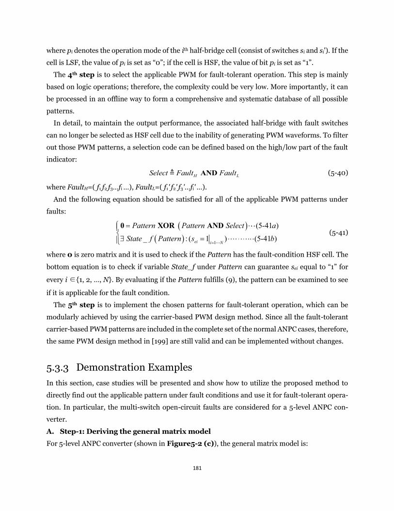
181
where pi denotes the operation mode of the ith half-bridge cell (consist of switches si and si'). If the
cell is LSF, the value of pi is set as “0”; if the cell is HSF, the value of bit pi is set as “1”.
The 4th step is to select the applicable PWM for fault-tolerant operation. This step is mainly
based on logic operations; therefore, the complexity could be very low. More importantly, it can
be processed in an offline way to form a comprehensive and systematic database of all possible
patterns.
In detail, to maintain the output performance, the associated half-bridge with fault switches
can no longer be selected as HSF cell due to the inability of generating PWM waveforms. To filter
out those PWM patterns, a selection code can be defined based on the high/low part of the fault
indicator:
H LSelect Fault FaultAND (5-40)
where FaultH=( f1 f2 f3…fi …), FaultL=( f1' f2' f3'…fi' …).
And the following equation should be satisfied for all of the applicable PWM patterns under
faults:
( )
( ) 1
(5-41 )
_ : ( 1 ) (5-41 )ei i N
Pattern Pattern Select a
State f Pattern s b=
= =
0 XOR AND (5-41)
where 0 is zero matrix and it is used to check if the Pattern has the fault-condition HSF cell. The
bottom equation is to check if variable State f under Pattern can guarantee sei equal to “1” for
every i ∈{1, 2, …, N}. By evaluating if the Pattern fulfills (9), the pattern can be examined to see
if it is applicable for the fault condition.
The 5th step is to implement the chosen patterns for fault-tolerant operation, which can be
modularly achieved by using the carrier-based PWM design method. Since all the fault-tolerant
carrier-based PWM patterns are included in the complete set of the normal ANPC cases, therefore,
the same PWM design method in [199] are still valid and can be implemented without changes.
5.3.3 Demonstration Examples
In this section, case studies will be presented and show how to utilize the proposed method to
directly find out the applicable pattern under fault conditions and use it for fault-tolerant opera-
tion. In particular, the multi-switch open-circuit faults are considered for a 5-level ANPC con-
verter.
A. Step-1: Deriving the general matrix model
For 5-level ANPC converter (shown in Figure5-2 (c)), the general matrix model is:
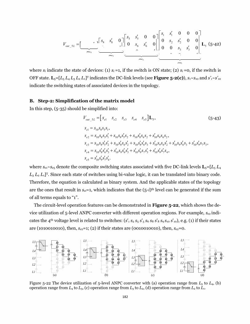
182
4
3
2
1
1 15 5
8 8 2 2_5 10 10 6 6 5
9 9 3 37 7
4 4
0 0 00 0
0 0 0 00 0
0 0 0 00 0
0 0 0
out L
s ss s
s s s sV s s s s
s s s ss s
s s
=
SGSG
SGSG
L _5 10 10 _5 10 10 V s s V s s _5 10 10V s s_5 10 10 _5 10 10 V s s _5 10 10 0 0 8 8 8 8
8 8 8 8 0 0 0 0
SG
9 9 9 9s s s s9 9s s9 9 9 9s s9 9 s s s s s s s s
0 0 0 0 0 0 0 0 0 0 0 0
SG
0 0 0 0 0 0
0 0 0 0 0 0 7 7 7 7 7 7 7 7 7 7 7 70 0 0 0 0 0 0 0 s s s s s s s s7 7s s7 7 7 7s s7 7 7 7s s7 7 7 7s s7 7 0 0 0 0 0 0 0 0 0 0 0 0
SG
0 0 0 0 0 0 0 0 4 4 4 40 0 0 0 0 0 s s s s4 4s s4 4 4 4s s4 4 0 0 0 0 0 0 0 0 0 0 0 0
SG
0 0 0 0 0 0 0 0 0 0 0 0 0 0 0 0 0 0
(5-42)
where si indicate the state of devices: (1) si =1, if the switch is ON state; (2) si =0, if the switch is
OFF state. L5=[L5 L4 L3 L2 L1]T indicates the DC-link levels (see Figure 5-2(c)), s1~s10 and s'1~s'10
indicate the switching states of associated devices in the topology.
B. Step-2: Simplification of the matrix model
In this step, (5-35) should be simplified into:
_ 5 1 2 3 4 5 5 ,out L e e e e eV s s s s s= L (5-43)
1 10 8 5 1
2 10 8 5 1 10 8 5 2 10 8 6 2 10 9 6 2
3 10 8 5 2 10 8 6 2 10 8 6 3 10 9 6 2 10 9 6 3 10 9 7 3
4 10 8 6 3 10 9 6 3 10 9 7 3 10 9 7 4
5
,,
,,
e
e
e
e
e
s s s s ss s s s s s s s s s s s s s s s ss s s s s s s s s s s s s s s s s s s s s s s s ss s s s s s s s s s s s s s s s ss s
=
= + + +
= + + + + +
= + + +
= 10 9 7 4.s s s
where se1~se5 denote the composite switching states associated with five DC-link levels L5=[L5 L4
L3 L2 L1]T. Since each state of switches using bi-value logic, it can be translated into binary code.
Therefore, the equation is calculated as binary system. And the applicable states of the topology
are the ones that result in sei=1, which indicates that the (5-i)th level can be generated if the sum
of all terms equals to “1”.
The circuit-level operation features can be demonstrated in Figure 5-22, which shows the de-
vice utilization of 5-level ANPC converter with different operation regions. For example, se2 indi-
cates the 4th voltage level is related to switches: (s'1 s2 s5 s'5 s6 s8 s'8 s9 s10 s'10), e.g. (1) if their states
are (1010010010), then, se2=1; (2) if their states are (0010010010), then, se2=0.
L4
L3
L2
L1
L5
L4
L3
L2
L1
L5
L4
L3
L2
L1
L5
L4
L3
L2
L1
L5
(a) (b) (c) (d) Figure 5-22 The device utilization of 5-level ANPC converter with (a) operation range from L5 to L4, (b) operation range from L4 to L3, (c) operation range from L3 to L2, (d) operation range from L2 to L1.
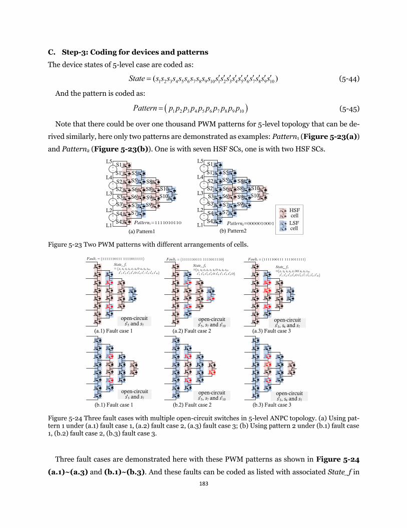
183
C. Step-3: Coding for devices and patterns
The device states of 5-level case are coded as:
1 2 3 4 5 6 7 8 9 10 1 2 3 4 5 6 7 8 9 10( )State s s s s s s s s s s s s s s s s s s s s = (5-44)
And the pattern is coded as:
( )1 2 3 4 5 6 7 8 9 10Pattern p p p p p p p p p p= (5-45)
Note that there could be over one thousand PWM patterns for 5-level topology that can be de-
rived similarly, here only two patterns are demonstrated as examples: Pattern1 (Figure 5-23(a))
and Pattern2 (Figure 5-23(b)). One is with seven HSF SCs, one is with two HSF SCs.
S1
S1'
S2S2'
S3S3'
S4
S4'
S5S5'
S6S6'
S7S7'
S8S8'
S9S9'
S10S10'
(a) Pattern1
L5
L4
L3
L2
L1
S1
S1'
S2S2'
S3S3'
S4
S4'
S5S5'
S6S6'
S7S7'
S8S8'
S9S9'
S10S10'
(b) Pattern2
HSF cell
LSF cell
L5
L4
L3
L2
L1Pattern1=1111010110 Pattern2=0000010001
Figure 5-23 Two PWM patterns with different arrangements of cells.
(a.1) Fault case 1
(b.1) Fault case 1
(a.2) Fault case 2
(b.2) Fault case 2
(a.3) Fault case 3
(b.3) Fault case 3
open-circuit s'5 and s7
open-circuit s'5 and s7
open-circuit s'5, s7 and s'10
open-circuit s'5, s7 and s'10
open-circuit s'5, s6 and s7
open-circuit s'5, s6 and s7
State_ f1 = (s1 s2 s3 s4 s5 s6 0 s8 s9 s10 s'1 s'2 s'3 s'4 0 s'6 s'7 s'8 s'9 s'10)
State_ f2 =(s1 s2 s3 s4 s5 s6 0 s8 s9 s10 s'1 s'2 s'3 s'4 0 s'6 s'7 s'8 s'9 0)
Fault1 = (1111110111 1111011111) Fault2 = (1111110111 1111011110)
State_ f3 =(s1 s2 s3 s4 s5 00 s8 s9 s10 s'1 s'2 s'3 s'4 0 s'6 s'7 s'8 s'9 s'10)
Fault3 = (1111100111 1111011111)
Figure 5-24 Three fault cases with multiple open-circuit switches in 5-level ANPC topology. (a) Using pat-tern 1 under (a.1) fault case 1, (a.2) fault case 2, (a.3) fault case 3; (b) Using pattern 2 under (b.1) fault case 1, (b.2) fault case 2, (b.3) fault case 3.
Three fault cases are demonstrated here with these PWM patterns as shown in Figure 5-24
(a.1)~(a.3) and (b.1)~(b.3). And these faults can be coded as listed with associated State f in
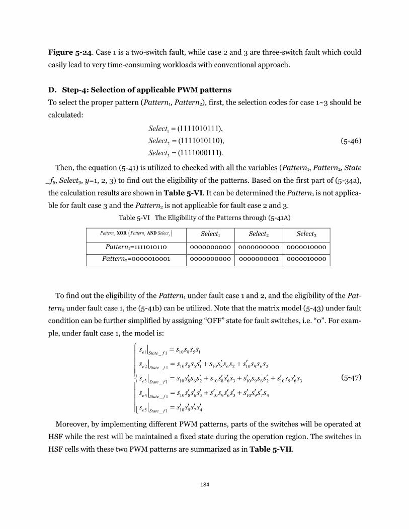
184
Figure 5-24. Case 1 is a two-switch fault, while case 2 and 3 are three-switch fault which could
easily lead to very time-consuming workloads with conventional approach.
D. Step-4: Selection of applicable PWM patterns
To select the proper pattern (Pattern1, Pattern2), first, the selection codes for case 1~3 should be
calculated:
1
2
3
(1111010111),(1111010110),(1111000111).
SelectSelectSelect
=
=
=
(5-46)
Then, the equation (5-41) is utilized to checked with all the variables (Pattern1, Pattern2, State
fy, Selecty, y=1, 2, 3) to find out the eligibility of the patterns. Based on the first part of (5-34a),
the calculation results are shown in Table 5-VI. It can be determined the Pattern1 is not applica-
ble for fault case 3 and the Pattern2 is not applicable for fault case 2 and 3.
Table 5-VI The Eligibility of the Patterns through (5-41A)
( ) x x yPattern Pattern SelectXOR AND Select1 Select2 Select3
Pattern1=1111010110 0000000000 0000000000 0000010000
Pattern2=0000010001 0000000000 0000000001 0000010000
To find out the eligibility of the Pattern1 under fault case 1 and 2, and the eligibility of the Pat-
tern2 under fault case 1, the (5-41b) can be utilized. Note that the matrix model (5-43) under fault
condition can be further simplified by assigning “OFF” state for fault switches, i.e. “0”. For exam-
ple, under fault case 1, the model is:
1 10 8 5 1_ 1
2 10 8 5 1 10 8 6 2 10 9 6 2_ 1
3 10 8 6 2 10 8 6 3 10 9 6 2 10 9 6 3_ 1
4 10 8 6 3 10 9 6 3 10 9 7 4_ 1
5 10 9 7 4_ 1
e State f
e State f
e State f
e State f
e State f
s s s s s
s s s s s s s s s s s s s
s s s s s s s s s s s s s s s s s
s s s s s s s s s s s s s
s s s s s
=
= + +
= + + +
= + +
=
(5-47)
Moreover, by implementing different PWM patterns, parts of the switches will be operated at
HSF while the rest will be maintained a fixed state during the operation region. The switches in
HSF cells with these two PWM patterns are summarized as in Table 5-VII.
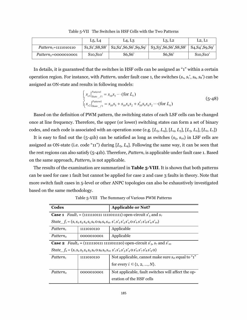
185
Table 5-VII The Switches in HSF Cells with the Two Patterns
L5, L4 L4, L3 L3, L2 L2, L1
Pattern1=1111010110 S1,S1',S8,S8' S2,S2',S6,S6',S9,S9' S3,S3',S6,S6',S8,S8' S4,S4',S9,S9'
Pattern2=0000010001 S10,S10' S6,S6' S6,S6' S10,S10'
In details, it is guaranteed that the switches in HSF cells can be assigned as “1” within a certain
operation region. For instance, with Pattern1 under fault case 1, the switches (s1, s1', s8, s8') can be
assigned as ON-state and results in following models: 1
1 10 5 5_ 1
12 10 5 10 6 2 10 9 6 2 4_ 1
(for )
(for )
Patterne State f
Patterne State f
s s s L
s s s s s s s s s s L
=
= + +
(5-48)
Based on the definition of PWM pattern, the switching states of each LSF cells can be changed
once at line frequency. Therefore, the upper (or lower) switching states can form a set of binary
codes, and each code is associated with an operation zone (e.g. [L5, L4], [L4, L3], [L3, L2], [L2, L1])
It is easy to find out the (5-41b) can be satisfied as long as switches (s5, s10) in LSF cells are
assigned as ON-state (i.e. code “11”) during [L5, L4]. Following the same way, it can be seen that
the rest regions can also satisfy (5-41b). Therefore, Pattern1 is applicable under fault case 1. Based
on the same approach, Pattern2 is not applicable.
The results of the examination are summarized in Table 5-VIII. It is shown that both patterns
can be used for case 1 fault but cannot be applied for case 2 and case 3 faults in theory. Note that
more switch fault cases in 5-level or other ANPC topologies can also be exhaustively investigated
based on the same methodology.
Table 5-VIII The Summary of Various PWM Patterns
Codes Applicable or Not?
Case 1 Fault1 = (1111110111 1111011111) open-circuit s'5 and s7
State_ f1 = (s1 s2 s3 s4 s5 s6 0 s8 s9 s10 s'1 s'2 s'3 s'4 0 s'6 s'7 s'8 s'9 s'10)
Pattern1 1111010110 Applicable
Pattern2 0000010001 Applicable
Case 2 Fault2 = (1111110111 1111011110) open-circuit s'5, s7 and s'10
State_ f2 = (s1 s2 s3 s4 s5 s6 0 s8 s9 s10 s'1 s'2 s'3 s'4 0 s'6 s'7 s'8 s'9 0)
Pattern1 1111010110 Not applicable, cannot make sure sei equal to “1”
for every i ∈{1, 2, …, N}.
Pattern2 0000010001 Not applicable, fault switches will affect the op-
eration of the HSF cells
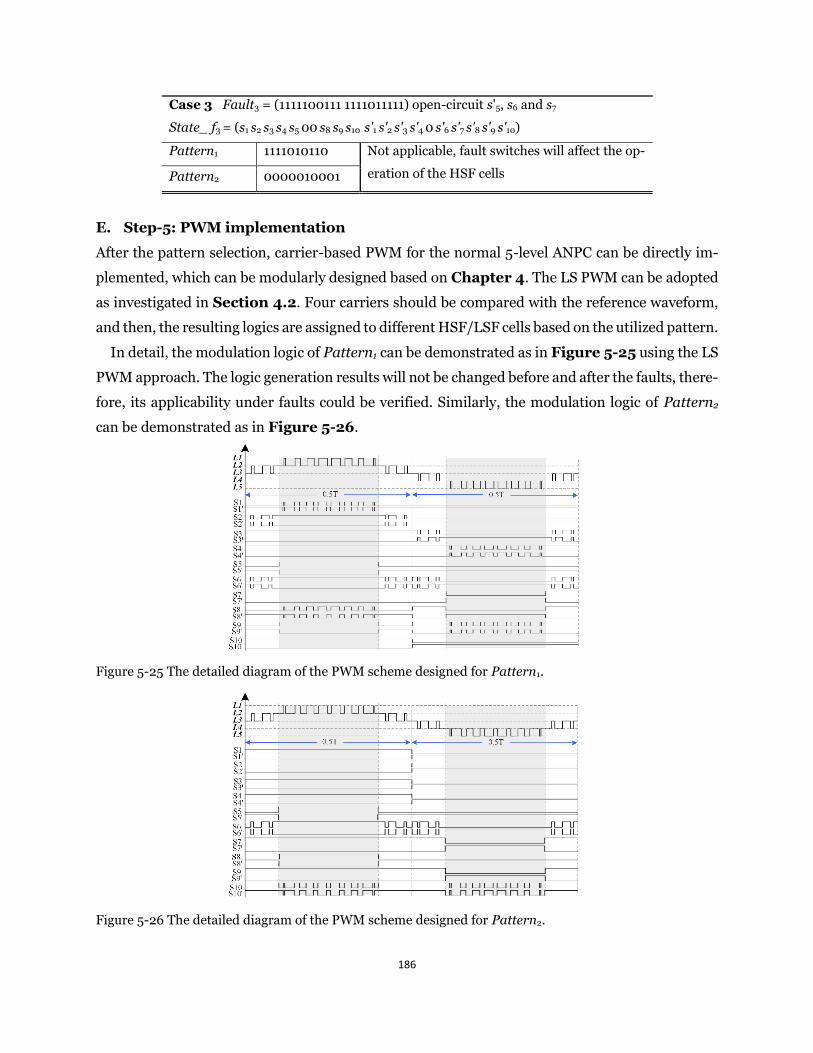
186
Case 3 Fault3 = (1111100111 1111011111) open-circuit s'5, s6 and s7
State_ f3 = (s1 s2 s3 s4 s5 00 s8 s9 s10 s'1 s'2 s'3 s'4 0 s'6 s'7 s'8 s'9 s'10)
Pattern1 1111010110 Not applicable, fault switches will affect the op-
eration of the HSF cells Pattern2 0000010001
E. Step-5: PWM implementation
After the pattern selection, carrier-based PWM for the normal 5-level ANPC can be directly im-
plemented, which can be modularly designed based on Chapter 4. The LS PWM can be adopted
as investigated in Section 4.2. Four carriers should be compared with the reference waveform,
and then, the resulting logics are assigned to different HSF/LSF cells based on the utilized pattern.
In detail, the modulation logic of Pattern1 can be demonstrated as in Figure 5-25 using the LS
PWM approach. The logic generation results will not be changed before and after the faults, there-
fore, its applicability under faults could be verified. Similarly, the modulation logic of Pattern2
can be demonstrated as in Figure 5-26.
Figure 5-25 The detailed diagram of the PWM scheme designed for Pattern1.
Figure 5-26 The detailed diagram of the PWM scheme designed for Pattern2.
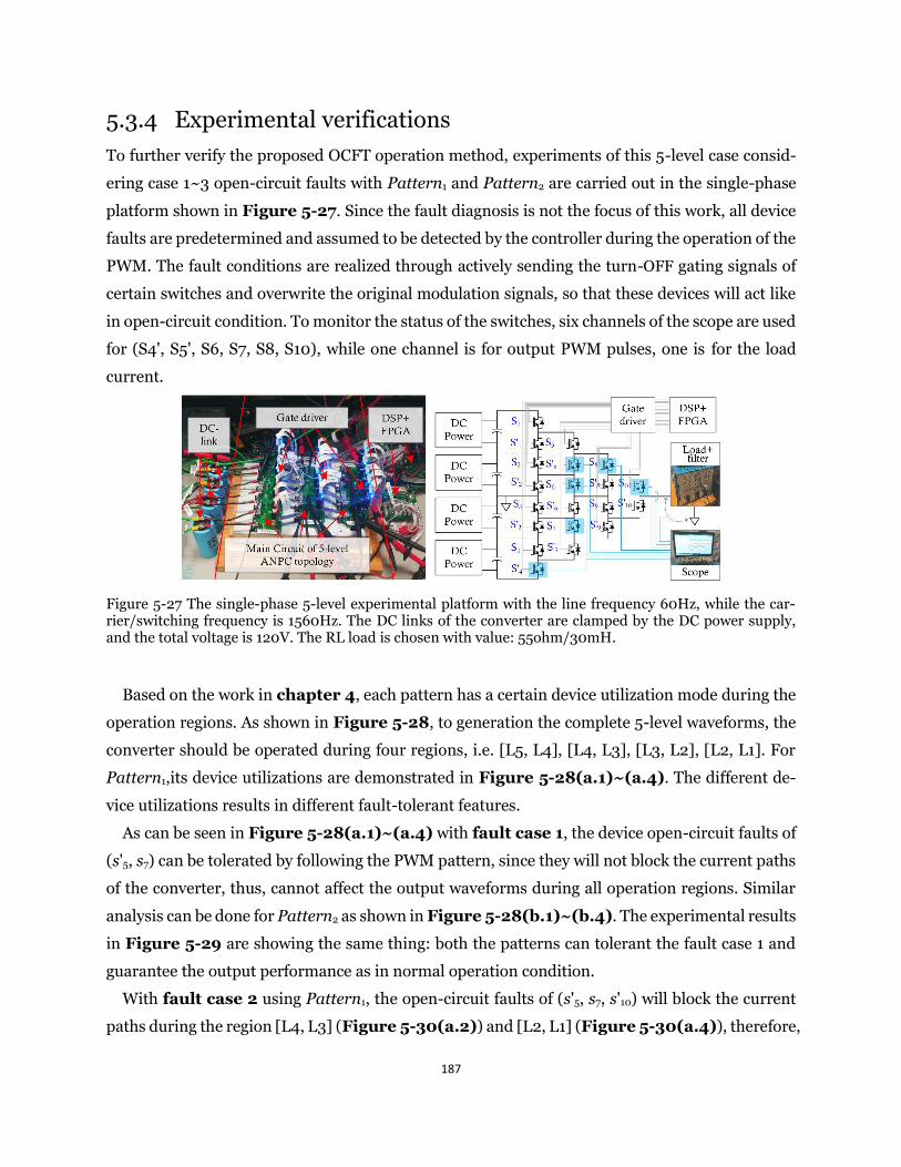
187
5.3.4 Experimental verifications
To further verify the proposed OCFT operation method, experiments of this 5-level case consid-
ering case 1~3 open-circuit faults with Pattern1 and Pattern2 are carried out in the single-phase
platform shown in Figure 5-27. Since the fault diagnosis is not the focus of this work, all device
faults are predetermined and assumed to be detected by the controller during the operation of the
PWM. The fault conditions are realized through actively sending the turn-OFF gating signals of
certain switches and overwrite the original modulation signals, so that these devices will act like
in open-circuit condition. To monitor the status of the switches, six channels of the scope are used
for (S4', S5', S6, S7, S8, S10), while one channel is for output PWM pulses, one is for the load
current.
Figure 5-27 The single-phase 5-level experimental platform with the line frequency 60Hz, while the car-rier/switching frequency is 1560Hz. The DC links of the converter are clamped by the DC power supply, and the total voltage is 120V. The RL load is chosen with value: 55ohm/30mH.
Based on the work in chapter 4, each pattern has a certain device utilization mode during the
operation regions. As shown in Figure 5-28, to generation the complete 5-level waveforms, the
converter should be operated during four regions, i.e. [L5, L4], [L4, L3], [L3, L2], [L2, L1]. For
Pattern1,its device utilizations are demonstrated in Figure 5-28(a.1)~(a.4). The different de-
vice utilizations results in different fault-tolerant features.
As can be seen in Figure 5-28(a.1)~(a.4) with fault case 1, the device open-circuit faults of
(s'5, s7) can be tolerated by following the PWM pattern, since they will not block the current paths
of the converter, thus, cannot affect the output waveforms during all operation regions. Similar
analysis can be done for Pattern2 as shown in Figure 5-28(b.1)~(b.4). The experimental results
in Figure 5-29 are showing the same thing: both the patterns can tolerant the fault case 1 and
guarantee the output performance as in normal operation condition.
With fault case 2 using Pattern1, the open-circuit faults of (s'5, s7, s'10) will block the current
paths during the region [L4, L3] (Figure 5-30(a.2)) and [L2, L1] (Figure 5-30(a.4)), therefore,
188
cannot make sure the output capability in theory. Situation is different for Pattern2, and the open-
circuit faults of (s'5, s7, s'10) will interfere the high frequency cells during the region [L5, L4] (Fig-
ure 5-30(b.1)) and [L2, L1] (Figure 5-30(b.4)), therefore, cannot be utilized during the fault
case 2. The experimental results in Figure 5-31 demonstrate the above analysis: neither of the
patterns can maintain the output performance after the fault case 2. The output voltage and load
current waveforms have obvious distortions. Note that Pattern1 under fault 2 can still operate the
converter with correct experimental waveforms in [L4, L3] as long as the output current is positive
and compatible with the conducting direction of the anti-parallel diode of the fault switch (s'10).
Due to the half-cycle symmetry in ANPC topologies, the output current could be negative in the
[L3, L2] and/or [L2, L1], when the anti-parallel diode of the fault switch (s'10) blocks the current
and cause distortions in output waveforms in Figure 5-31(a).
As for fault case 3, the open-circuit faults of (s'5, s6, s7) will block the current paths during the
region [L5, L4] for both patterns as shown in Figure 5-32(a.1) and (b.1). In addition, it is easy
to see that the open-circuit faults of (s'5, s6, s7) will interfere the operation of the high frequency
cells in both patterns. The disturbed operation regions are [L4, L3] (Figure 5-32(a.2) and (b.2))
and [L3, L2] (Figure 5-32(a.3) and (b.3)). Therefore, the intended operation cannot be realized
in a right way. The experimental results in Figure 5-33 verify this: obvious distortions can be
seen in the output voltage and load current waveforms in both patterns.
In summary, systematic analysis and selection for applicable carrier-based PWM patterns are
achieved in a mathematical way. By using such a tool, the applicable PWM patterns of fault-con-
dition ANPC converter can be systematically derived. Therefore, random enumeration and non-
systematic case-by-case design can be avoided for ANPC converters. Without losing the generality,
the 5-level cases with multiple open-circuit fault switches are discussed as examples. The experi-
mental results show that the output levels can be appropriately produced with the selected appli-
cable PWM pattern, especially under multiple switch open-circuit faults.
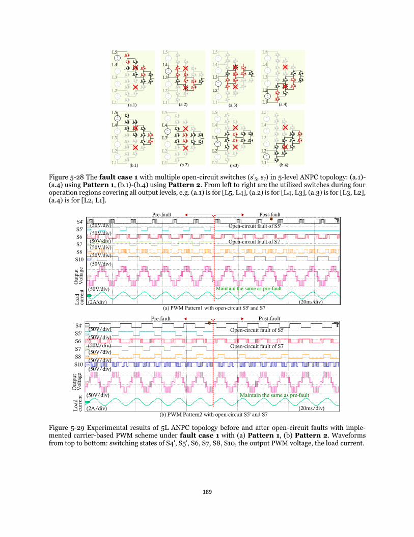
189
L5
L4
L3
L2
L1
L5
L4
L3
L2
L1
L5
L4
L3
L2
L1
L5
L4
L3
L2
L1
L5
L4
L3
L2
L1
L5
L4
L3
L2
L1
L5
L4
L3
L2
L1
L5
L4
L3
L2
L1
(a.1) (a.2) (a.3) (a.4)
(b.1) (b.2) (b.3) (b.4) Figure 5-28 The fault case 1 with multiple open-circuit switches (s'5, s7) in 5-level ANPC topology: (a.1)-(a.4) using Pattern 1, (b.1)-(b.4) using Pattern 2. From left to right are the utilized switches during four operation regions covering all output levels, e.g. (a.1) is for [L5, L4], (a.2) is for [L4, L3], (a.3) is for [L3, L2], (a.4) is for [L2, L1].
Open-circuit fault of S5'
Open-circuit fault of S7
Maintain the same as pre-fault
S5'S4'
S6S7S8S10
Out
put
Vol
tage
Load
cu
rren
t (50V/div)
(2A/div) (20ms/div)
(50V/div)(50V/div)(50V/div)(50V/div)(50V/div)(50V/div)
(a) PWM Pattern1 with open-circuit S5' and S7
Pre-fault Post-fault
Open-circuit fault of S5'
Open-circuit fault of S7
Maintain the same as pre-fault
(b) PWM Pattern2 with open-circuit S5' and S7
Pre-fault Post-fault
S5'S4'
S6S7S8S10
Out
put
Vol
tage
Loa
d cu
rren
t (50V/div)
(2A/div) (20ms/div)
(50V/div)
(50V/div)
(50V/div)(50V/div)
(50V/div)
(50V/div)
Figure 5-29 Experimental results of 5L ANPC topology before and after open-circuit faults with imple-mented carrier-based PWM scheme under fault case 1 with (a) Pattern 1, (b) Pattern 2. Waveforms from top to bottom: switching states of S4', S5', S6, S7, S8, S10, the output PWM voltage, the load current.
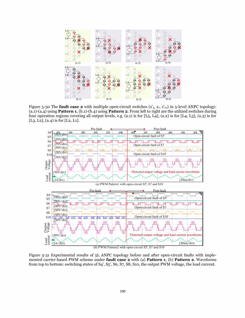
190
L5
L4
L3
L2
L1
L5
L4
L3
L2
L1
L5
L4
L3
L2
L1
L5
L4
L3
L2
L1
L5
L4
L3
L2
L1
L5
L4
L3
L2
L1
L5
L4
L3
L2
L1
L5
L4
L3
L2
L1
(a.1) (a.2) (a.3) (a.4)
(b.1) (b.2) (b.3) (b.4)
Figure 5-30 The fault case 2 with multiple open-circuit switches (s'5, s7, s'10) in 5-level ANPC topology: (a.1)-(a.4) using Pattern 1, (b.1)-(b.4) using Pattern 2. From left to right are the utilized switches during four operation regions covering all output levels, e.g. (a.1) is for [L5, L4], (a.2) is for [L4, L3], (a.3) is for [L3, L2], (a.4) is for [L2, L1].
Open-circuit fault of S5'
Open-circuit fault of S7
Open-circuit fault of S10'
Distorted output voltage and load current waveforms
S5'S4'
S6S7S8
S10
Out
put
Vol
tage
Load
cu
rren
t (50V/div)
(2A/div) (20ms/div)
(50V/div)(50V/div)(50V/div)(50V/div)(50V/div)(50V/div)
(a) PWM Pattern1 with open-circuit S5', S7 and S10
Pre-fault Post-fault
Open-circuit fault of S5'
Open-circuit fault of S7
Open-circuit fault of S10'
(b) PWM Pattern2 with open-circuit S5', S7 and S10
Distorted output voltage and load current waveforms
Pre-fault Post-fault
S5'S4'
S6S7S8S10
Out
put
Vol
tage
Loa
d cu
rren
t (50V/div)
(2A/div) (20ms/div)
(50V/div)
(50V/div)
(50V/div)(50V/div)
(50V/div)(50V/div)
Figure 5-31 Experimental results of 5L ANPC topology before and after open-circuit faults with imple-mented carrier-based PWM scheme under fault case 2 with (a) Pattern 1, (b) Pattern 2. Waveforms from top to bottom: switching states of S4', S5', S6, S7, S8, S10, the output PWM voltage, the load current.
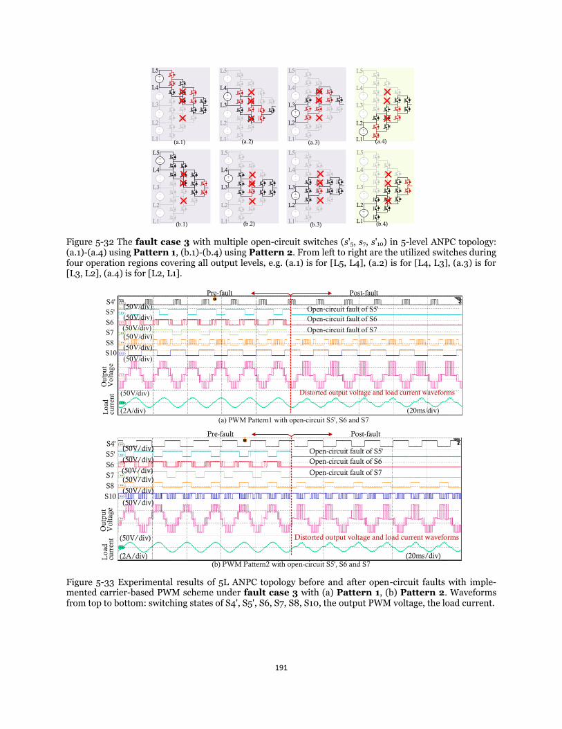
191
L5
L4
L3
L2
L1
L5
L4
L3
L2
L1
L5
L4
L3
L2
L1
L5
L4
L3
L2
L1
L5
L4
L3
L2
L1
L5
L4
L3
L2
L1
L5
L4
L3
L2
L1
L5
L4
L3
L2
L1
(a.1) (a.2) (a.3) (a.4)
(b.1) (b.2) (b.3) (b.4)
Figure 5-32 The fault case 3 with multiple open-circuit switches (s'5, s7, s'10) in 5-level ANPC topology: (a.1)-(a.4) using Pattern 1, (b.1)-(b.4) using Pattern 2. From left to right are the utilized switches during four operation regions covering all output levels, e.g. (a.1) is for [L5, L4], (a.2) is for [L4, L3], (a.3) is for [L3, L2], (a.4) is for [L2, L1].
Open-circuit fault of S5'
Open-circuit fault of S7Open-circuit fault of S6
S5'S4'
S6S7S8S10
Out
put
Vol
tage
Load
cu
rren
t (50V/div)
(2A/div) (20ms/div)
(50V/div)(50V/div)(50V/div)(50V/div)(50V/div)(50V/div)
(a) PWM Pattern1 with open-circuit S5', S6 and S7
Distorted output voltage and load current waveforms
Pre-fault Post-fault
Open-circuit fault of S5'
Open-circuit fault of S7
Open-circuit fault of S6
(b) PWM Pattern2 with open-circuit S5', S6 and S7
Distorted output voltage and load current waveforms
Pre-fault Post-fault
S5'S4'
S6S7S8S10
Out
put
Vol
tage
Loa
d cu
rren
t (50V/div)
(2A/div) (20ms/div)
(50V/div)
(50V/div)
(50V/div)(50V/div)
(50V/div)
(50V/div)
Figure 5-33 Experimental results of 5L ANPC topology before and after open-circuit faults with imple-mented carrier-based PWM scheme under fault case 3 with (a) Pattern 1, (b) Pattern 2. Waveforms from top to bottom: switching states of S4', S5', S6, S7, S8, S10, the output PWM voltage, the load current.

192
5.4. Summary
Following the works in Chapter 3 and Chapter 4, the matrix models as well as the associated
systematic PWM design method are implemented in a synergic way to help realize two different
tasks: (1) the topology simplification, (2) fault-tolerant operation.
For the first task, some special matrices are used to systematically derive the simplified circuit
of ANPC converters under certain PWM pattern. In such a way, the topology simplification can
be decoupled with the PWM design process. The predesigned PWM schemes can directly operate
the simplified converter without modification. In addition, the cross-topology isomorphism can
be implemented to further facilitate the derivation process by hierarchically utilizing the low-level
simplified circuits.
For the second task, both the general and the simplified matrix models are implemented along
with a step-by-step logic-based procedure. The main focus is on the open-circuit type with multi-
ple fault switches. After the systematic coding and calculation, the applicable PWM patterns of an
arbitrary ANPC topology with fault switches can be identified. In such a way, the PWM pattern
database can be predesigned and directly implemented after the fault-tolerant analysis. Therefore,
random enumeration and non-systematic case-by-case design can be avoided for ANPC convert-
ers.
In these two tasks, both 4-level and 5-level case studies have been carried out to verify the pro-
posed method for ANPC converters. Besides, this design method, particularly the matrix model
concept, can potentially inspire similar PWM design method for other topologies, which can be
studied in future.
193
Chapter 6 Conclusions and Future plans
6.1. Achievements of this work
In this work, four different levels of achievements have been achieved: theory level, circuit level,
structure level, and PWM level.
A. Theory level achievements
In theory level, the fundamental relationships of power converters are thoroughly investigated in
Chapter 2, especially for VSCs and CSCs. Two major types of theories are highlighted: one is the
famous dual theory, the other one is the emerging isomorphic theory. Then, instead of implement-
ing the dual methods and isomorphic methods in an independent way, we use both the duality
and isomorphism synthetically and discover the topology cycling phenomenon. Such a new find-
ing reveals the common properties among various VSCs and CSCs in terms of their topologies,
operation principles, modulation/control strategies, etc. To demonstrate the cycling rules, the
theoretical proof is given to show the versatility of these new findings for VSCs and CSCs.
B. Circuit level achievements
In circuit level, the dual theory for planar circuits and non-planar circuits is reviewed. Especially
for non-planar circuits, various methods have been proposed in the literature and are systemati-
cally summarized. To overcome the limitations, additional constraints are normally needed for
dual transformation of those converters.
Then, the isomorphic theory is introduced for establishing another intrinsic relationship among
VSCs and CSCs. Not only the topology but also the operation rules (e.g. modulation) can be trans-
formed from one converter to another. In particular, the single-phase three-level VSC is isomor-
phic with the three-phase CSC, and they share the one-to-one modulation scheme as verified in
this work.
Based on the theory-level discovery, the systematic operation analysis and the unified model of
selected examples are given to show the similarities among the cycling VSC and CSC topologies.
The modulation scheme of the DC-series H-bridge CSC is designed to reduce the DC ripples based
on the existing PWM of the existing VSC topology. In summary, by properly utilizing the
194
discovered relationships, both existing and future topologies can be linked with each other and
sharing the existing knowledge in a more comprehensive way.
C. Structure level achievements
In structure level, the fundamental relationships of MLCs are introduced in Chapter 3: (i) the
dual structures in voltage-source MLCs and current-source MLCs, (ii) the equivalent structures
in matrix-type MLCs regarding voltage-source MLCs and current-source MLCs. Furthermore, the
MLCs can be abstractly represented in unified matrix models using the concept of stage.
With the stage-based common structure, the systematic design of MLCs can be realized for all
kinds of MLCs universally. In details, the node-branch forms are obtained for some most com-
monly studied topologies, which not only demonstrate the duality between voltage-source and
current-source multilevel topologies, but also the logical equivalence of multilevel indirect and
direct matrix converters. The matrix presentations of MLCs are derived from their node-branch
forms, which provides an opportunity for systematic analysis of different MLCs. It can help the
simplification process of derived various MLC topologies, and can also facilitate the modulation
implementation for different MLCs, especially matrix converters, through the logic mapping.
Moreover, compared to the current approach of manual design and analysis, the design rules
of the proposed method are more general and straightforward to follow even for researchers with-
out a strong power electronics background. With the proposed method, a unified design platform
could be established, which opens the potential for both manual synthesis/derivation and com-
puter-aided design/analysis. Several multilevel topologies are derived as examples, e.g. internal
paralleled MLCs, 7L hybrid MLCs and 9L MLCs with auxiliary circuits. The discussions with prac-
tical considerations and experiments are given to further demonstrate the feasibility of the pro-
posed method.
D. PWM level achievements
In PWM level, several achievements have been done:
Firstly, in Chapter 4, universal carrier-based PWM design methods are proposed for non-
modular MLCs through hierarchical decomposition of the converter topologies. Two important
concepts are introduced: identical circuits between two converters and identical circuits within a
single converter.
To deal with the non-modularity of the MLCs, the sub-topologies are decomposed in a hierar-
chical way by iteratively using the identical circuits between two converters. Then, an exhaustive
list of CPWM schemes can be designed. The demonstration of the proposed method is mainly
195
done for ANPC converters. It features some advantages over conventional case-by-case methods:
(1) It is a universal and offline design method regards CB-PWM schemes, and it can be easily
implemented for MLCs once the pattern is selected. (2) An exhaustive list of CB-PWM schemes
can be designed which provides an opportunity to enhance the system by the adoption of different
PWM strategies according to different application requirements. (3) The low-level PWM schemes
can be utilized for high-level PWM design which can significantly reduce the design complexity
and guarantee the control modularity. Several designed PWM schemes under different operation
modes are verified through experiments and demonstrate how the same approach can also be
generalized for high-level ANPC topologies (e.g. 3L to 4L, 4L to 5L).
On the other hand, the identical circuits within a single converter are utilized and demonstrated
in ANPC converter for the novel PS-PWM methods. It is based on different operation principles
from the conventional methods for flying-capacitor-based, cascaded H-bridge, or modular multi-
level converter. With more evenly distributed switching actions among all devices, the designed
PS PWM schemes feature better utilization of devices and higher ESF compared with conven-
tional LS PWM. Moreover, high-level PWM schemes can be synthesized through low-level
schemes. In such a way, the PS PWM design for ANPC topology can be realized modularly for both
the general and the simplified ANPC converters. Besides, the extensibility and reduced computa-
tion burden make the proposed method very suitable for multi-level ANPC topologies (e.g., 4- and
5-level). The five-level PS PWM scheme is designed with experimental validation and thorough
discussions and comparisons, which shows a better performance regards device utilization and
loss distribution.
Then, in Chapter 5, following the works in Chapter 3 and Chapter 4, the matrix modeling
as well as the associated systematic PWM design method are implemented in a synergic way to
help realize two different tasks: (1) the topology simplification, (2) fault-tolerant operation.
For the first task, some special matrices are used to systematically derive the simplified circuit
of ANPC converters under certain PWM pattern. In such a way, the topology simplification can
be decoupled with the PWM design process. The predesigned PWM schemes can directly operate
the simplified converter without modification. In addition, the cross-topology isomorphism can
be implemented to further facilitate the derivation process by hierarchically utilizing the low-level
simplified circuits.
For the second task, both the general and the simplified matrix models are implemented along
with a step-by-step logic-based procedure. The main focus is on the open-circuit type with multi-
ple fault switches. After the systematic coding and calculation, the applicable PWM patterns of an
arbitrary ANPC topology with fault switches can be identified. In such a way, the PWM pattern
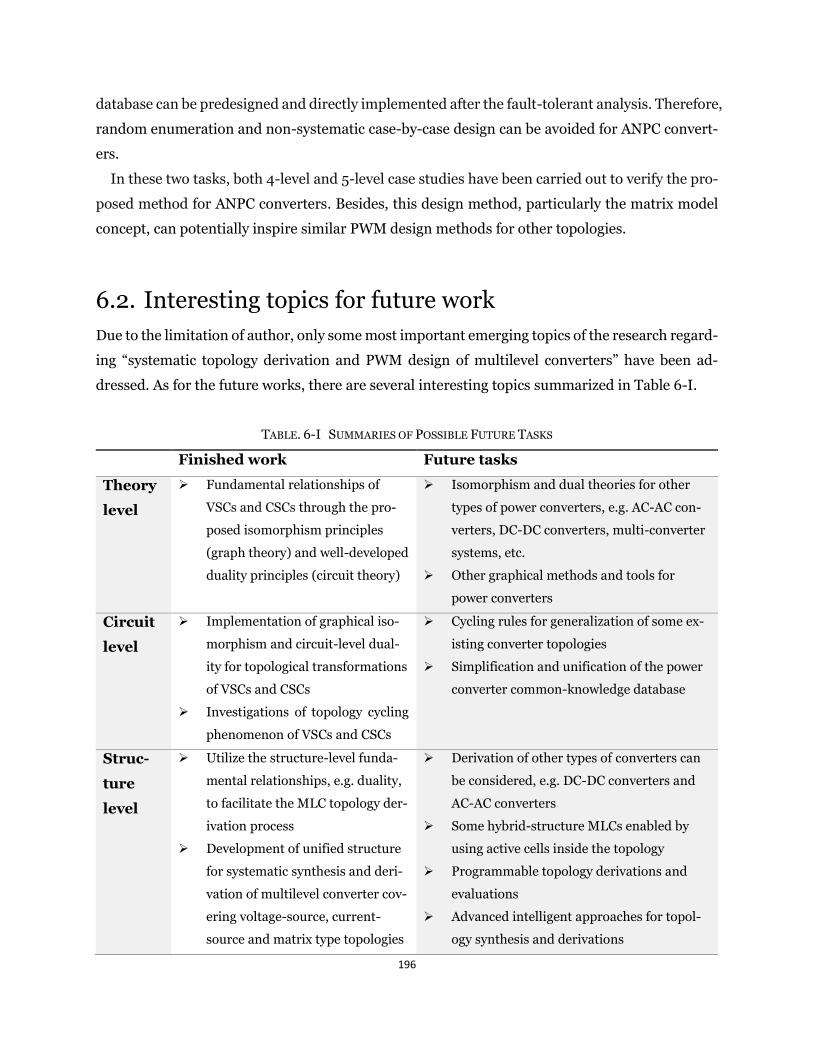
196
database can be predesigned and directly implemented after the fault-tolerant analysis. Therefore,
random enumeration and non-systematic case-by-case design can be avoided for ANPC convert-
ers.
In these two tasks, both 4-level and 5-level case studies have been carried out to verify the pro-
posed method for ANPC converters. Besides, this design method, particularly the matrix model
concept, can potentially inspire similar PWM design methods for other topologies.
6.2. Interesting topics for future work
Due to the limitation of author, only some most important emerging topics of the research regard-
ing “systematic topology derivation and PWM design of multilevel converters” have been ad-
dressed. As for the future works, there are several interesting topics summarized in Table 6-I.
TABLE. 6-I SUMMARIES OF POSSIBLE FUTURE TASKS
Finished work Future tasks
Theory
level
➢ Fundamental relationships of
VSCs and CSCs through the pro-
posed isomorphism principles
(graph theory) and well-developed
duality principles (circuit theory)
➢ Isomorphism and dual theories for other
types of power converters, e.g. AC-AC con-
verters, DC-DC converters, multi-converter
systems, etc.
➢ Other graphical methods and tools for
power converters
Circuit
level
➢ Implementation of graphical iso-
morphism and circuit-level dual-
ity for topological transformations
of VSCs and CSCs
➢ Investigations of topology cycling
phenomenon of VSCs and CSCs
➢ Cycling rules for generalization of some ex-
isting converter topologies
➢ Simplification and unification of the power
converter common-knowledge database
Struc-
ture
level
➢ Utilize the structure-level funda-
mental relationships, e.g. duality,
to facilitate the MLC topology der-
ivation process
➢ Development of unified structure
for systematic synthesis and deri-
vation of multilevel converter cov-
ering voltage-source, current-
source and matrix type topologies
➢ Derivation of other types of converters can
be considered, e.g. DC-DC converters and
AC-AC converters
➢ Some hybrid-structure MLCs enabled by
using active cells inside the topology
➢ Programmable topology derivations and
evaluations
➢ Advanced intelligent approaches for topol-
ogy synthesis and derivations
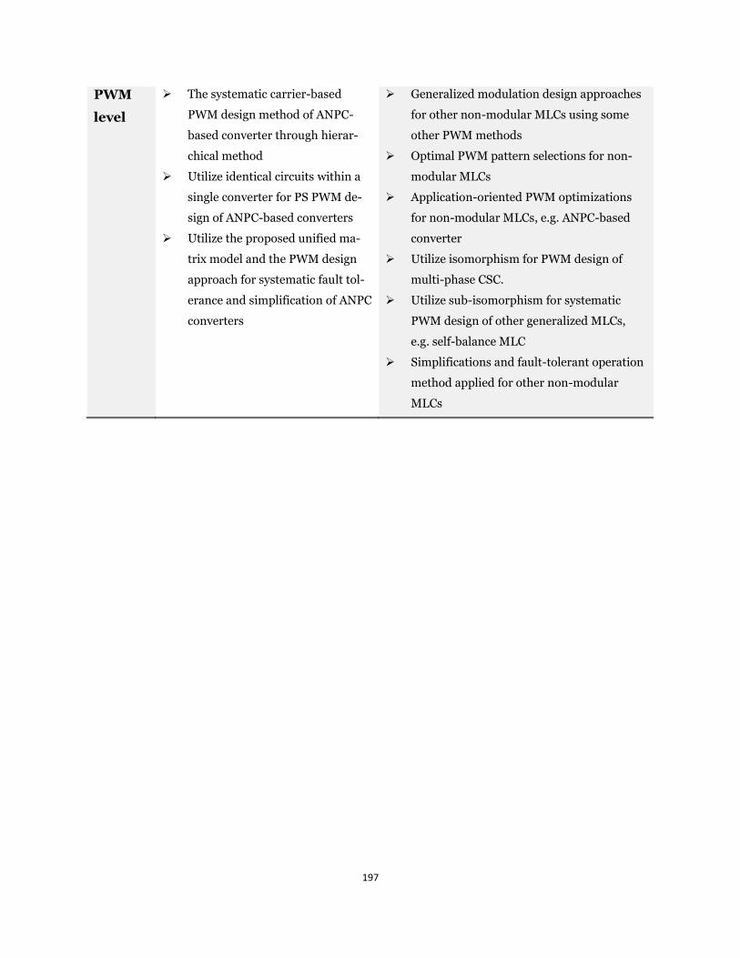
197
PWM
level
➢ The systematic carrier-based
PWM design method of ANPC-
based converter through hierar-
chical method
➢ Utilize identical circuits within a
single converter for PS PWM de-
sign of ANPC-based converters
➢ Utilize the proposed unified ma-
trix model and the PWM design
approach for systematic fault tol-
erance and simplification of ANPC
converters
➢ Generalized modulation design approaches
for other non-modular MLCs using some
other PWM methods
➢ Optimal PWM pattern selections for non-
modular MLCs
➢ Application-oriented PWM optimizations
for non-modular MLCs, e.g. ANPC-based
converter
➢ Utilize isomorphism for PWM design of
multi-phase CSC.
➢ Utilize sub-isomorphism for systematic
PWM design of other generalized MLCs,
e.g. self-balance MLC
➢ Simplifications and fault-tolerant operation
method applied for other non-modular
MLCs
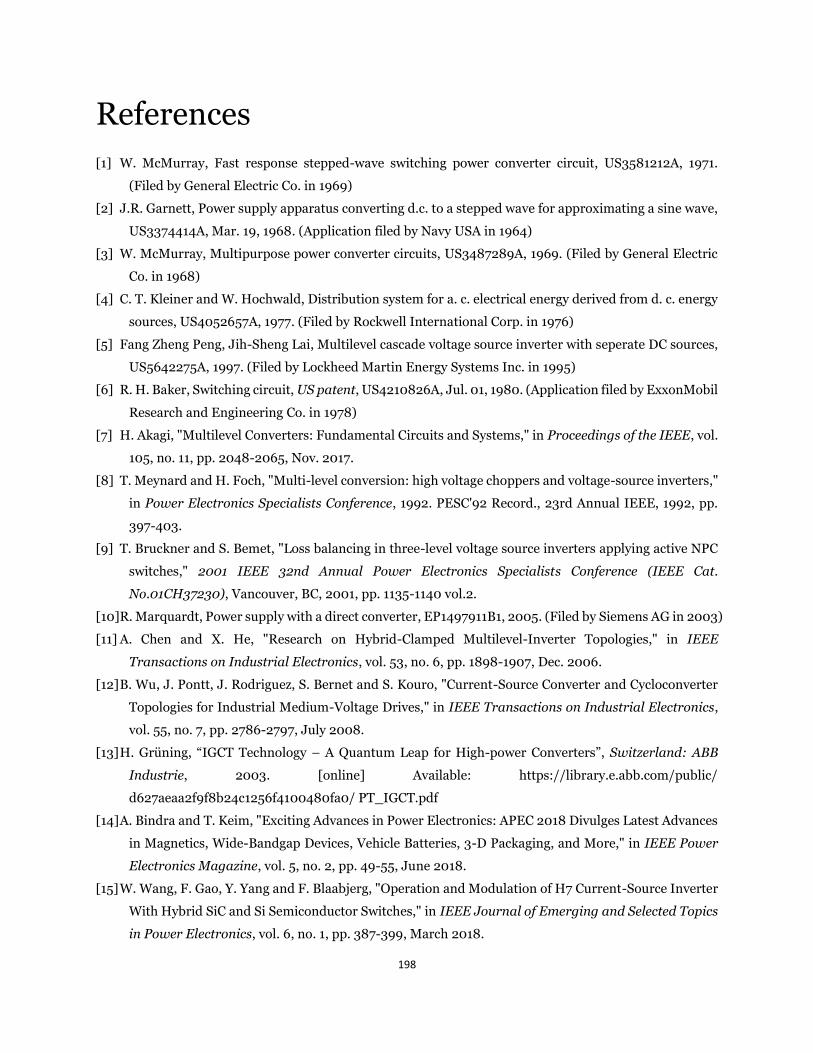
198
References
[1] W. McMurray, Fast response stepped-wave switching power converter circuit, US3581212A, 1971.
(Filed by General Electric Co. in 1969)
[2] J.R. Garnett, Power supply apparatus converting d.c. to a stepped wave for approximating a sine wave,
US3374414A, Mar. 19, 1968. (Application filed by Navy USA in 1964)
[3] W. McMurray, Multipurpose power converter circuits, US3487289A, 1969. (Filed by General Electric
Co. in 1968)
[4] C. T. Kleiner and W. Hochwald, Distribution system for a. c. electrical energy derived from d. c. energy
sources, US4052657A, 1977. (Filed by Rockwell International Corp. in 1976)
[5] Fang Zheng Peng, Jih-Sheng Lai, Multilevel cascade voltage source inverter with seperate DC sources,
US5642275A, 1997. (Filed by Lockheed Martin Energy Systems Inc. in 1995)
[6] R. H. Baker, Switching circuit, US patent, US4210826A, Jul. 01, 1980. (Application filed by ExxonMobil
Research and Engineering Co. in 1978)
[7] H. Akagi, "Multilevel Converters: Fundamental Circuits and Systems," in Proceedings of the IEEE, vol.
105, no. 11, pp. 2048-2065, Nov. 2017.
[8] T. Meynard and H. Foch, "Multi-level conversion: high voltage choppers and voltage-source inverters,"
in Power Electronics Specialists Conference, 1992. PESC'92 Record., 23rd Annual IEEE, 1992, pp.
397-403.
[9] T. Bruckner and S. Bemet, "Loss balancing in three-level voltage source inverters applying active NPC
switches," 2001 IEEE 32nd Annual Power Electronics Specialists Conference (IEEE Cat.
No.01CH37230), Vancouver, BC, 2001, pp. 1135-1140 vol.2.
[10] R. Marquardt, Power supply with a direct converter, EP1497911B1, 2005. (Filed by Siemens AG in 2003)
[11] A. Chen and X. He, "Research on Hybrid-Clamped Multilevel-Inverter Topologies," in IEEE
Transactions on Industrial Electronics, vol. 53, no. 6, pp. 1898-1907, Dec. 2006.
[12] B. Wu, J. Pontt, J. Rodriguez, S. Bernet and S. Kouro, "Current-Source Converter and Cycloconverter
Topologies for Industrial Medium-Voltage Drives," in IEEE Transactions on Industrial Electronics,
vol. 55, no. 7, pp. 2786-2797, July 2008.
[13] H. Grüning, “IGCT Technology – A Quantum Leap for High-power Converters”, Switzerland: ABB
Industrie, 2003. [online] Available: https://library.e.abb.com/public/
d627aeaa2f9f8b24c1256f4100480fa0/ PT_IGCT.pdf
[14] A. Bindra and T. Keim, "Exciting Advances in Power Electronics: APEC 2018 Divulges Latest Advances
in Magnetics, Wide-Bandgap Devices, Vehicle Batteries, 3-D Packaging, and More," in IEEE Power
Electronics Magazine, vol. 5, no. 2, pp. 49-55, June 2018.
[15] W. Wang, F. Gao, Y. Yang and F. Blaabjerg, "Operation and Modulation of H7 Current-Source Inverter
With Hybrid SiC and Si Semiconductor Switches," in IEEE Journal of Emerging and Selected Topics
in Power Electronics, vol. 6, no. 1, pp. 387-399, March 2018.
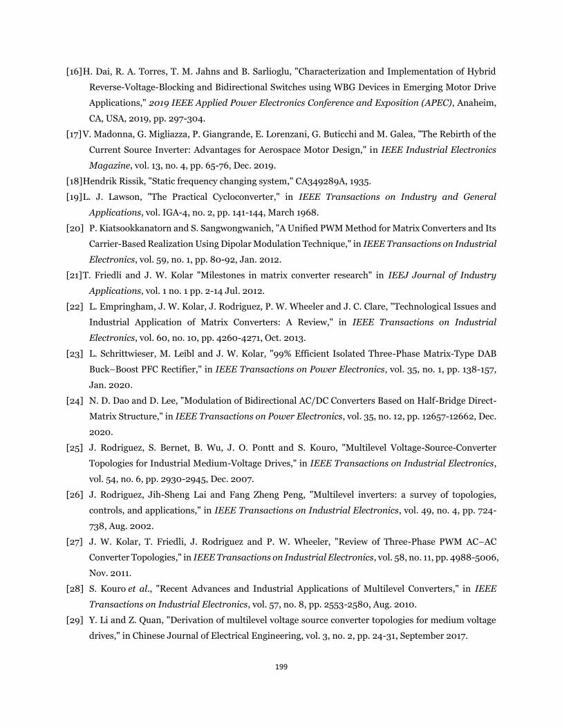
199
[16] H. Dai, R. A. Torres, T. M. Jahns and B. Sarlioglu, "Characterization and Implementation of Hybrid
Reverse-Voltage-Blocking and Bidirectional Switches using WBG Devices in Emerging Motor Drive
Applications," 2019 IEEE Applied Power Electronics Conference and Exposition (APEC), Anaheim,
CA, USA, 2019, pp. 297-304.
[17] V. Madonna, G. Migliazza, P. Giangrande, E. Lorenzani, G. Buticchi and M. Galea, "The Rebirth of the
Current Source Inverter: Advantages for Aerospace Motor Design," in IEEE Industrial Electronics
Magazine, vol. 13, no. 4, pp. 65-76, Dec. 2019.
[18] Hendrik Rissik, "Static frequency changing system," CA349289A, 1935.
[19] L. J. Lawson, "The Practical Cycloconverter," in IEEE Transactions on Industry and General
Applications, vol. IGA-4, no. 2, pp. 141-144, March 1968.
[20] P. Kiatsookkanatorn and S. Sangwongwanich, "A Unified PWM Method for Matrix Converters and Its
Carrier-Based Realization Using Dipolar Modulation Technique," in IEEE Transactions on Industrial
Electronics, vol. 59, no. 1, pp. 80-92, Jan. 2012.
[21] T. Friedli and J. W. Kolar "Milestones in matrix converter research" in IEEJ Journal of Industry
Applications, vol. 1 no. 1 pp. 2-14 Jul. 2012.
[22] L. Empringham, J. W. Kolar, J. Rodriguez, P. W. Wheeler and J. C. Clare, "Technological Issues and
Industrial Application of Matrix Converters: A Review," in IEEE Transactions on Industrial
Electronics, vol. 60, no. 10, pp. 4260-4271, Oct. 2013.
[23] L. Schrittwieser, M. Leibl and J. W. Kolar, "99% Efficient Isolated Three-Phase Matrix-Type DAB
Buck–Boost PFC Rectifier," in IEEE Transactions on Power Electronics, vol. 35, no. 1, pp. 138-157,
Jan. 2020.
[24] N. D. Dao and D. Lee, "Modulation of Bidirectional AC/DC Converters Based on Half-Bridge Direct-
Matrix Structure," in IEEE Transactions on Power Electronics, vol. 35, no. 12, pp. 12657-12662, Dec.
2020.
[25] J. Rodriguez, S. Bernet, B. Wu, J. O. Pontt and S. Kouro, "Multilevel Voltage-Source-Converter
Topologies for Industrial Medium-Voltage Drives," in IEEE Transactions on Industrial Electronics,
vol. 54, no. 6, pp. 2930-2945, Dec. 2007.
[26] J. Rodriguez, Jih-Sheng Lai and Fang Zheng Peng, "Multilevel inverters: a survey of topologies,
controls, and applications," in IEEE Transactions on Industrial Electronics, vol. 49, no. 4, pp. 724-
738, Aug. 2002.
[27] J. W. Kolar, T. Friedli, J. Rodriguez and P. W. Wheeler, "Review of Three-Phase PWM AC–AC
Converter Topologies," in IEEE Transactions on Industrial Electronics, vol. 58, no. 11, pp. 4988-5006,
Nov. 2011.
[28] S. Kouro et al., "Recent Advances and Industrial Applications of Multilevel Converters," in IEEE
Transactions on Industrial Electronics, vol. 57, no. 8, pp. 2553-2580, Aug. 2010.
[29] Y. Li and Z. Quan, "Derivation of multilevel voltage source converter topologies for medium voltage
drives," in Chinese Journal of Electrical Engineering, vol. 3, no. 2, pp. 24-31, September 2017.
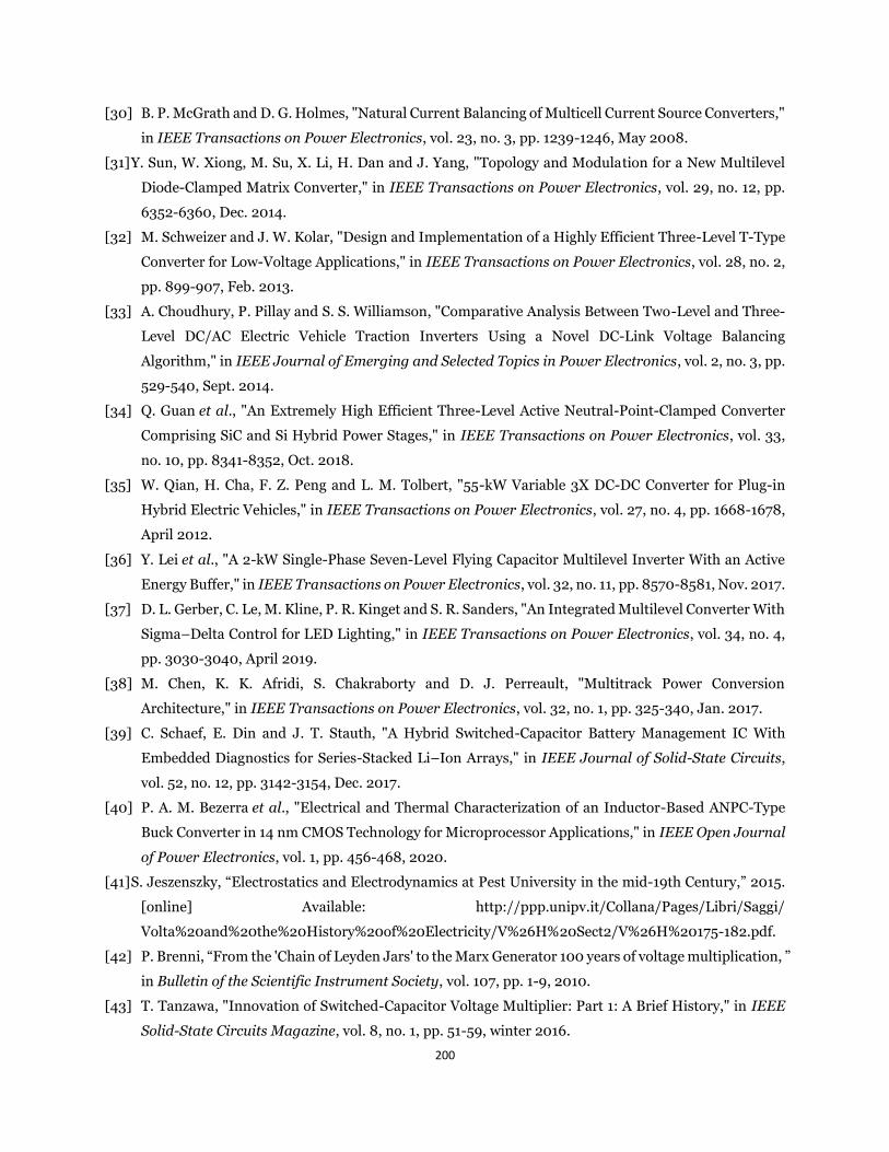
200
[30] B. P. McGrath and D. G. Holmes, "Natural Current Balancing of Multicell Current Source Converters,"
in IEEE Transactions on Power Electronics, vol. 23, no. 3, pp. 1239-1246, May 2008.
[31] Y. Sun, W. Xiong, M. Su, X. Li, H. Dan and J. Yang, "Topology and Modulation for a New Multilevel
Diode-Clamped Matrix Converter," in IEEE Transactions on Power Electronics, vol. 29, no. 12, pp.
6352-6360, Dec. 2014.
[32] M. Schweizer and J. W. Kolar, "Design and Implementation of a Highly Efficient Three-Level T-Type
Converter for Low-Voltage Applications," in IEEE Transactions on Power Electronics, vol. 28, no. 2,
pp. 899-907, Feb. 2013.
[33] A. Choudhury, P. Pillay and S. S. Williamson, "Comparative Analysis Between Two-Level and Three-
Level DC/AC Electric Vehicle Traction Inverters Using a Novel DC-Link Voltage Balancing
Algorithm," in IEEE Journal of Emerging and Selected Topics in Power Electronics, vol. 2, no. 3, pp.
529-540, Sept. 2014.
[34] Q. Guan et al., "An Extremely High Efficient Three-Level Active Neutral-Point-Clamped Converter
Comprising SiC and Si Hybrid Power Stages," in IEEE Transactions on Power Electronics, vol. 33,
no. 10, pp. 8341-8352, Oct. 2018.
[35] W. Qian, H. Cha, F. Z. Peng and L. M. Tolbert, "55-kW Variable 3X DC-DC Converter for Plug-in
Hybrid Electric Vehicles," in IEEE Transactions on Power Electronics, vol. 27, no. 4, pp. 1668-1678,
April 2012.
[36] Y. Lei et al., "A 2-kW Single-Phase Seven-Level Flying Capacitor Multilevel Inverter With an Active
Energy Buffer," in IEEE Transactions on Power Electronics, vol. 32, no. 11, pp. 8570-8581, Nov. 2017.
[37] D. L. Gerber, C. Le, M. Kline, P. R. Kinget and S. R. Sanders, "An Integrated Multilevel Converter With
Sigma–Delta Control for LED Lighting," in IEEE Transactions on Power Electronics, vol. 34, no. 4,
pp. 3030-3040, April 2019.
[38] M. Chen, K. K. Afridi, S. Chakraborty and D. J. Perreault, "Multitrack Power Conversion
Architecture," in IEEE Transactions on Power Electronics, vol. 32, no. 1, pp. 325-340, Jan. 2017.
[39] C. Schaef, E. Din and J. T. Stauth, "A Hybrid Switched-Capacitor Battery Management IC With
Embedded Diagnostics for Series-Stacked Li–Ion Arrays," in IEEE Journal of Solid-State Circuits,
vol. 52, no. 12, pp. 3142-3154, Dec. 2017.
[40] P. A. M. Bezerra et al., "Electrical and Thermal Characterization of an Inductor-Based ANPC-Type
Buck Converter in 14 nm CMOS Technology for Microprocessor Applications," in IEEE Open Journal
of Power Electronics, vol. 1, pp. 456-468, 2020.
[41] S. Jeszenszky, “Electrostatics and Electrodynamics at Pest University in the mid-19th Century,” 2015.
[online] Available: http://ppp.unipv.it/Collana/Pages/Libri/Saggi/
Volta%20and%20the%20History%20of%20Electricity/V%26H%20Sect2/V%26H%20175-182.pdf.
[42] P. Brenni, “From the 'Chain of Leyden Jars' to the Marx Generator 100 years of voltage multiplication, ”
in Bulletin of the Scientific Instrument Society, vol. 107, pp. 1-9, 2010.
[43] T. Tanzawa, "Innovation of Switched-Capacitor Voltage Multiplier: Part 1: A Brief History," in IEEE
Solid-State Circuits Magazine, vol. 8, no. 1, pp. 51-59, winter 2016.
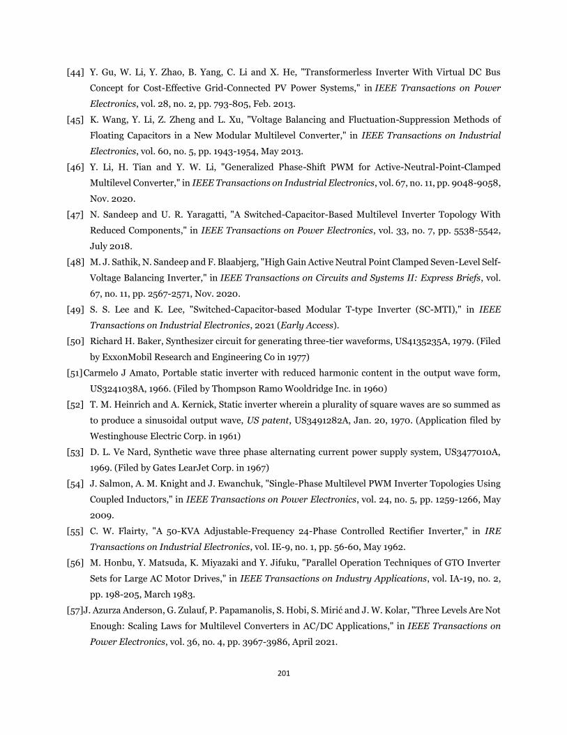
201
[44] Y. Gu, W. Li, Y. Zhao, B. Yang, C. Li and X. He, "Transformerless Inverter With Virtual DC Bus
Concept for Cost-Effective Grid-Connected PV Power Systems," in IEEE Transactions on Power
Electronics, vol. 28, no. 2, pp. 793-805, Feb. 2013.
[45] K. Wang, Y. Li, Z. Zheng and L. Xu, "Voltage Balancing and Fluctuation-Suppression Methods of
Floating Capacitors in a New Modular Multilevel Converter," in IEEE Transactions on Industrial
Electronics, vol. 60, no. 5, pp. 1943-1954, May 2013.
[46] Y. Li, H. Tian and Y. W. Li, "Generalized Phase-Shift PWM for Active-Neutral-Point-Clamped
Multilevel Converter," in IEEE Transactions on Industrial Electronics, vol. 67, no. 11, pp. 9048-9058,
Nov. 2020.
[47] N. Sandeep and U. R. Yaragatti, "A Switched-Capacitor-Based Multilevel Inverter Topology With
Reduced Components," in IEEE Transactions on Power Electronics, vol. 33, no. 7, pp. 5538-5542,
July 2018.
[48] M. J. Sathik, N. Sandeep and F. Blaabjerg, "High Gain Active Neutral Point Clamped Seven-Level Self-
Voltage Balancing Inverter," in IEEE Transactions on Circuits and Systems II: Express Briefs, vol.
67, no. 11, pp. 2567-2571, Nov. 2020.
[49] S. S. Lee and K. Lee, "Switched-Capacitor-based Modular T-type Inverter (SC-MTI)," in IEEE
Transactions on Industrial Electronics, 2021 (Early Access).
[50] Richard H. Baker, Synthesizer circuit for generating three-tier waveforms, US4135235A, 1979. (Filed
by ExxonMobil Research and Engineering Co in 1977)
[51] Carmelo J Amato, Portable static inverter with reduced harmonic content in the output wave form,
US3241038A, 1966. (Filed by Thompson Ramo Wooldridge Inc. in 1960)
[52] T. M. Heinrich and A. Kernick, Static inverter wherein a plurality of square waves are so summed as
to produce a sinusoidal output wave, US patent, US3491282A, Jan. 20, 1970. (Application filed by
Westinghouse Electric Corp. in 1961)
[53] D. L. Ve Nard, Synthetic wave three phase alternating current power supply system, US3477010A,
1969. (Filed by Gates LearJet Corp. in 1967)
[54] J. Salmon, A. M. Knight and J. Ewanchuk, "Single-Phase Multilevel PWM Inverter Topologies Using
Coupled Inductors," in IEEE Transactions on Power Electronics, vol. 24, no. 5, pp. 1259-1266, May
2009.
[55] C. W. Flairty, "A 50-KVA Adjustable-Frequency 24-Phase Controlled Rectifier Inverter," in IRE
Transactions on Industrial Electronics, vol. IE-9, no. 1, pp. 56-60, May 1962.
[56] M. Honbu, Y. Matsuda, K. Miyazaki and Y. Jifuku, "Parallel Operation Techniques of GTO Inverter
Sets for Large AC Motor Drives," in IEEE Transactions on Industry Applications, vol. IA-19, no. 2,
pp. 198-205, March 1983.
[57] J. Azurza Anderson, G. Zulauf, P. Papamanolis, S. Hobi, S. Mirić and J. W. Kolar, "Three Levels Are Not
Enough: Scaling Laws for Multilevel Converters in AC/DC Applications," in IEEE Transactions on
Power Electronics, vol. 36, no. 4, pp. 3967-3986, April 2021.
202
[58] H. Wang, H. Wang, G. Zhu and F. Blaabjerg, "An Overview of Capacitive DC-Links-Topology
Derivation and Scalability Analysis," in IEEE Transactions on Power Electronics, vol. 35, no. 2, pp.
1805-1829, Feb. 2020.
[59] Z. Quan, Y. Li and Y. Li, "Internal paralleled active neutral point clamped converter with logic-based
flying capacitor voltage balancing," 2017 IEEE 18th Workshop on Control and Modeling for Power
Electronics (COMPEL), Stanford, CA, 2017, pp. 1-6.
[60] Z. Quan and Y. W. Li, "Multilevel Voltage-Source Converter Topologies With Internal Parallel
Modularity," in IEEE Transactions on Industry Applications, vol. 56, no. 1, pp. 378-389, Jan.-Feb.
2020.
[61] H. E. Martin, Output-transformerless static inverter, US3514688A, 1970. (Filed by United Technologies
Corp. in 1968)
[62] T. Corry, Method of and apparatus for generating three-phase sinusoidal voltages, US3725767A, 1973.
(Filed by Motors Liquidation Co. in 1971)
[63] D. J. Hucker and N. L. Schmitz, Inverter for providing a sinusodial output having a low harmonic
content, US4063144A, 1977. (Filed by Sundstrand Corp. in 1976)
[64] Gui-Jia Su, "Multilevel DC-link inverter," in IEEE Transactions on Industry Applications, vol. 41, no.
3, pp. 848-854, May-June 2005.
[65] P. R. Bana, K. P. Panda, R. T. Naayagi, P. Siano and G. Panda, "Recently Developed Reduced Switch
Multilevel Inverter for Renewable Energy Integration and Drives Application: Topologies,
Comprehensive Analysis and Comparative Evaluation," in IEEE Access, vol. 7, pp. 54888-54909, 2019.
[66] M. Vijeh, M. Rezanejad, E. Samadaei and K. Bertilsson, "A General Review of Multilevel Inverters
Based on Main Submodules: Structural Point of View," in IEEE Transactions on Power Electronics,
vol. 34, no. 10, pp. 9479-9502, Oct. 2019.
[67] H. Fujita, "A three-phase voltage-source solar power conditioner using a single-phase PWM control
method," 2009 IEEE Energy Conversion Congress and Exposition, San Jose, CA, 2009, pp. 3748-
3754.
[68] Q. Lei and F. Z. Peng, "Space Vector Pulsewidth Amplitude Modulation for a Buck–Boost
Voltage/Current Source Inverter," in IEEE Transactions on Power Electronics, vol. 29, no. 1, pp. 266-
274, Jan. 2014.
[69] J.W. Kolar, M. Guacci, M. Antivachis, D. Bortis, Advanced 3 Φ SiC GaN PWM Inverter Concepts for
Future VSD Applications, 2020. [online] Available: https://www.pes-
publications.ee.ethz.ch/uploads/tx_ethpublications.
[70] K. Hermanns, Y. Peng and A. Mantooth, "The Increasing Role of Design Automation in Power
Electronics: Gathering What Is Needed," in IEEE Power Electronics Magazine, vol. 7, no. 1, pp. 46-
50, March 2020.
[71] A. J. Marques Cardoso, "Power Electronics Design Methods and Automation in the Digital Era:
Evolution of Design Automation Tools," in IEEE Power Electronics Magazine, vol. 7, no. 2, pp. 36-
40, June 2020.
203
[72] N. Rashidi, Q. Wang, R. Burgos, C. Roy and D. Boroyevich, "Multi-objective Design and Optimization
of Power Electronics Converters With Uncertainty Quantification—Part I: Parametric Uncertainty,"
in IEEE Transactions on Power Electronics, vol. 36, no. 2, pp. 1463-1474, Feb. 2021.
[73] J. W. Kolar, F. Krismer, "Power Electronics Design 4.0," IEEE Design Automation for Power
Electronics Workshop (DAPE), Portland (OR), USA, September 22, 2018. [online] Available:
https://www.pes-publications.ee.ethz.ch/publications/workshopsseminars
[74] Q. M. Li, F. C. Lee and T. G. Wilson, "Design verification and testing of power supply system by using
virtual prototype," in IEEE Transactions on Power Electronics, vol. 18, no. 3, pp. 733-739, May 2003.
[75] S. Zhao, F. Blaabjerg and H. Wang, "An Overview of Artificial Intelligence Applications for Power
Electronics," in IEEE Transactions on Power Electronics, vol. 36, no. 4, pp. 4633-4658, April 2021.
[76] P. M. Bhagwat and V. R. Stefanovic, "Generalized Structure of a Multilevel PWM Inverter," in IEEE
Transactions on Industry Applications, vol. IA-19, no. 6, pp. 1057-1069, Nov. 1983.
[77] N. S. Choi, J. G. Cho and G. H. Cho, "A general circuit topology of multilevel inverter," PESC '91 Record
22nd Annual IEEE Power Electronics Specialists Conference, Cambridge, MA, USA, 1991, pp. 96-103.
[78] Fang Zheng Peng, "A generalized multilevel inverter topology with self voltage balancing," in IEEE
Transactions on Industry Applications, vol. 37, no. 2, pp. 611-618, March-April 2001.
[79] E. Najafi and A. H. M. Yatim, "Design and Implementation of a New Multilevel Inverter Topology," in
IEEE Transactions on Industrial Electronics, vol. 59, no. 11, pp. 4148-4154, Nov. 2012.
[80] X. Yuan, "Derivation of Voltage Source Multilevel Converter Topologies," in IEEE Transactions on
Industrial Electronics, vol. 64, no. 2, pp. 966-976, Feb. 2017.
[81] Z. Bai and Z. Zhang, "Conformation of Multilevel Current Source Converter Topologies Using the
Duality Principle," in IEEE Transactions on Power Electronics, vol. 23, no. 5, pp. 2260-2267, Sept.
2008.
[82] A. Nami, J. Liang, F. Dijkhuizen and G. D. Demetriades, "Modular Multilevel Converters for HVDC
Applications: Review on Converter Cells and Functionalities," in IEEE Transactions on Power
Electronics, vol. 30, no. 1, pp. 18-36, Jan. 2015.
[83] J. I. Leon, S. Kouro, L. G. Franquelo, J. Rodriguez and B. Wu, "The Essential Role and the Continuous
Evolution of Modulation Techniques for Voltage-Source Inverters in the Past, Present, and Future
Power Electronics," in IEEE Transactions on Industrial Electronics, vol. 63, no. 5, pp. 2688-2701,
May 2016.
[84] J. I. Leon, S. Vazquez and L. G. Franquelo, "Multilevel Converters: Control and Modulation
Techniques for Their Operation and Industrial Applications," in Proceedings of the IEEE, vol. 105, no.
11, pp. 2066-2081, Nov. 2017.
[85] B. P. McGrath and D. G. Holmes, "Multicarrier PWM strategies for multilevel inverters," in IEEE
Transactions on Industrial Electronics, vol. 49, no. 4, pp. 858-867, Aug. 2002.
[86] O. Ojo, "The generalized discontinuous PWM scheme for three-phase voltage source inverters," in
IEEE Transactions on Industrial Electronics, vol. 51, no. 6, pp. 1280-1289, Dec. 2004.
204
[87] S. Busquets-Monge, S. Alepuz, J. Rocabert and J. Bordonau, "Pulsewidth Modulations for the
Comprehensive Capacitor Voltage Balance of n-Level Three-Leg Diode-Clamped Converters," in IEEE
Transactions on Power Electronics, vol. 24, no. 5, pp. 1364-1375, May 2009.
[88] T. Geyer, N. Oikonomou, G. Papafotiou and F. D. Kieferndorf, "Model Predictive Pulse Pattern
Control," in IEEE Transactions on Industry Applications, vol. 48, no. 2, pp. 663-676, March-April
2012.
[89] A. Edpuganti and A. K. Rathore, "A Survey of Low Switching Frequency Modulation Techniques for
Medium-Voltage Multilevel Converters," in IEEE Transactions on Industry Applications, vol. 51, no.
5, pp. 4212-4228, Sept.-Oct. 2015.
[90] A. K. Gupta and A. M. Khambadkone, "A Space Vector PWM Scheme for Multilevel Inverters Based
on Two-Level Space Vector PWM," in IEEE Transactions on Industrial Electronics, vol. 53, no. 5, pp.
1631-1639, Oct. 2006.
[91] Y. Deng, K. H. Teo, C. Duan, T. G. Habetler and R. G. Harley, "A Fast and Generalized Space Vector
Modulation Scheme for Multilevel Inverters," in IEEE Transactions on Power Electronics, vol. 29,
no. 10, pp. 5204-5217, Oct. 2014.
[92] N. Celanovic and D. Boroyevich, "A comprehensive study of neutral-point voltage balancing problem
in three-level neutral-point-clamped voltage source PWM inverters," in IEEE Transactions on Power
Electronics, vol. 15, no. 2, pp. 242-249, March 2000.
[93] L. Ding, Z. Quan and Y. W. Li, "Common-Mode Voltage Reduction for Parallel CSC-Fed Motor Drives
With Multilevel Modulation," in IEEE Transactions on Power Electronics, vol. 33, no. 8, pp. 6555-
6566, Aug. 2018.
[94] J. Pou et al., "Fast-Processing Modulation Strategy for the Neutral-Point-Clamped Converter With
Total Elimination of Low-Frequency Voltage Oscillations in the Neutral Point," in IEEE Transactions
on Industrial Electronics, vol. 54, no. 4, pp. 2288-2294, Aug. 2007.
[95] J. Pou, J. Zaragoza, S. Ceballos, M. Saeedifard and D. Boroyevich, "A Carrier-Based PWM Strategy
With Zero-Sequence Voltage Injection for a Three-Level Neutral-Point-Clamped Converter," in IEEE
Transactions on Power Electronics, vol. 27, no. 2, pp. 642-651, Feb. 2012.
[96] S. Busquets-Monge and J. Nicolas-Apruzzese, "A Multilevel Active-Clamped Converter Topology—
Operating Principle," in IEEE Transactions on Industrial Electronics, vol. 58, no. 9, pp. 3868-3878,
Sept. 2011.
[97] Y. Jiao and F. C. Lee, "New Modulation Scheme for Three-Level Active Neutral-Point-Clamped
Converter With Loss and Stress Reduction," in IEEE Transactions on Industrial Electronics, vol. 62,
no. 9, pp. 5468-5479, Sept. 2015.
[98] D. Zhang, J. He and S. Madhusoodhanan, "Three-level two-stage decoupled active NPC converter with
Si IGBT and SiC MOSFET," 2017 IEEE Energy Conversion Congress and Exposition (ECCE),
Cincinnati, OH, 2017, pp. 5671-5678.
205
[99] Y. Li, Y. Wang and B. Q. Li, "Generalized Theory of Phase-Shifted Carrier PWM for Cascaded H-Bridge
Converters and Modular Multilevel Converters," in IEEE Journal of Emerging and Selected Topics
in Power Electronics, vol. 4, no. 2, pp. 589-605, June 2016.
[100] R. Naderi, A. K. Sadigh and K. M. Smedley, "Dual Flying Capacitor Active-Neutral-Point-Clamped
Multilevel Converter," in IEEE Transactions on Power Electronics, vol. 31, no. 9, pp. 6476-6484, Sept.
2016.
[101] C. Li, S. Wang, Q. Guan and D. Xu, "Hybrid Modulation Concept for Five-Level Active-Neutral-Point-
Clamped Converter," in IEEE Transactions on Power Electronics, vol. 32, no. 12, pp. 8958-8962, Dec.
2017.
[102] A. Dekka, R. L. Fuentes, M. Narimani and B. Wu, "Voltage Balancing of a Modular Neutral-Point-
Clamped Converter With a Carrier-Based Modulation Scheme," in IEEE Transactions on Power
Electronics, vol. 33, no. 10, pp. 8208-8212, Oct. 2018.
[103] H. Tian and Y. W. Li, "Carrier-Based Stair Edge PWM (SEPWM) for Capacitor Balancing in Multilevel
Converters With Floating Capacitors," in IEEE Transactions on Industry Applications, vol. 54, no. 4,
pp. 3440-3452, July-Aug. 2018.
[104] K. Wang, Z. Zheng, L. Xu and Y. Li, "An Optimized Carrier-Based PWM Method and Voltage
Balancing Control for Five-Level ANPC Converters," in IEEE Transactions on Industrial Electronics,
vol. 67, no. 11, pp. 9120-9132, Nov. 2020.
[105] D. Zhou, Z. Quan and Y. Li, "Simplified Predictive Duty Cycle Control of Multilevel Converters With
Internal Identical Structure," in IEEE Transactions on Power Electronics, vol. 35, no. 11, pp. 12416-
12428, Nov. 2020.
[106] W. E. Newell, "Power Electronics---Emerging from Limbo," in IEEE Transactions on Industry
Applications, vol. IA-10, no. 1, pp. 7-11, Jan. 1974.
[107] J. D. van Wyk and F. C. Lee, "On a Future for Power Electronics," in IEEE Journal of Emerging and
Selected Topics in Power Electronics, vol. 1, no. 2, pp. 59-72, June 2013.
[108] E. Castellani and D. Rickles, "Introduction to special issue on dualities," Studies in History and
Philosophy of Science Part B: Studies in History and Philosophy of Modern Physics, vol. 59, pp. 1-5,
Aug 2017.
[109] Charles-Augustin Coulomb, "First memoir on electricity and magnetism," French Acad. Sci., pp. 569–
577 1788. Translated by Louis L. Bucciarelli, Emeritus Professor of Engineering and Technology
Studies (MIT), MIT, 2000 (revised and notes added by Christine Blondel and Bertrand Wolff, 2012).
online [Available]: http://www.ampere.cnrs.fr/i-corpuspic/tab/Sources/coulomb/Coulomb_
El_1785.pdf.
[110] William Francis Magie, A Source Book in Physics. Cambridge, Harvard University Press, 1935.
[111] L. Weinberg, "Kirchhoff's 'Third and Fourth Laws'," in IRE Transactions on Circuit Theory, vol. 5, no.
1, pp. 8-30, March 1958.
[112] M. Parodi and M. Storace, Linear and Nonlinear Circuits: Basic & Advanced Concepts, Springer
International Publishing, 2018.
206
[113] J.P. Dowling, C.P. Williams and J.D. Franson, "Maxwell duality, lorentz invariance, and topological
phase," Phys. Rev. Lett., vol. 83, no. 13, pp. 2486-2489, September 27, 1999.
[114] N.K. Dadhich, "Electromagnetic duality in general relativity," General Relativity and Gravitation,
New York, vol. 32, pp. 1009-1023, 1999.
[115] A. Russell, A treatise on the theory of alternating currents, 2nd ed. Cambridge, University Press, 1914.
[116] W. Cauer, “Topological duality theorems and reciprocity theorems of circuit theory,” J. Appl. Math.
Mechanics, vol. 14, pp. 349–350, 1934.
[117] E.C. Cherry, "The duality between interlinked electric and magnetic circuits and the formation of
transformer equivalent circuits," Proc. Phys. Soc. B, vol. 62, no. 2, pp. 101–111, February 1949.
[118] S. D. Freeland, "Techniques for the practical application of duality to power circuits," in IEEE
Transactions on Power Electronics, vol. 7, no. 2, pp. 374-384, April 1992.
[119] J. W. Kolar, H. Ertl and F. C. Zach, "Analysis of the duality of three phase PWM converters with DC
voltage link and DC current link," Conference Record of the IEEE Industry Applications Society
Annual Meeting,, San Diego, CA, USA, 1989, pp. 724-737 vol.1.
[120] P. A. Dahono, T. Kataoka and Y. Sato, "Dual relationships between voltage-source and current-source
three-phase inverters and its applications," Proceedings of Second International Conference on
Power Electronics and Drive Systems, Singapore, 1997, pp. 559-565 vol.2.
[121] A. Bloch, "On methods for the construction of networks dual to non-planar networks," Proceedings
of the Physical Society, vol. 58, no. 6, pp. 677-694, Nov 1, 1946.
[122] F. Harary, "Some historical and intuitive aspects of graph theory," in Society for Industrial and
Applied Mathematics Review, vol. 2, no. 2, pp. 123-131, April 1, 1960.
[123] L.R. Foulds, Graph Theory Applications. New York, NY, Springer New York, 1992.
[124] F. Dörfler, J. W. Simpson-Porco and F. Bullo, "Electrical Networks and Algebraic Graph Theory:
Models, Properties, and Applications," in Proceedings of the IEEE, vol. 106, no. 5, pp. 977-1005, May
2018.
[125] T. Ishizaki, A. Chakrabortty and J. Imura, "Graph-Theoretic Analysis of Power Systems,"
in Proceedings of the IEEE, vol. 106, no. 5, pp. 931-952, May 2018.
[126] A. K. Srivastava, T. A. Ernster, R. Liu and V. G. Krishnan, "Graph-theoretic algorithms for cyber-
physical vulnerability analysis of power grid with incomplete information," in Journal of Modern
Power Systems and Clean Energy, vol. 6, no. 5, pp. 887-899, September 2018.
[127] R. Razi, M. -C. Pham, A. Hably, S. Bacha, Q. -T. Tran and H. Iman-Eini, "A Novel Graph-Based
Routing Algorithm in Residential Multimicrogrid Systems," in IEEE Transactions on Industrial
Informatics, vol. 17, no. 3, pp. 1774-1784, March 2021.
[128] M. Liserre, V. Raveendran and M. Andresen, "Graph-Theory-Based Modeling and Control for System-
Level Optimization of Smart Transformers," in IEEE Transactions on Industrial Electronics, vol. 67,
no. 10, pp. 8910-8920, Oct. 2020.
[129] H. Whitney, "2-isomorphic graphs," American journal of mathematics, vol. 55, no. 1/4, pp. 245-254
1933.
207
[130] G.H. Moore, "The evolution of the concept of homeomorphism," Historia mathematica, vol. 34, no.
3, pp. 333-343 2007.
[131] C.T. G. Hahn, Graph homomorphisms: Structure and symmetry. Springer, Dordrecht, 1997.
[132] R.C. Read and D.G. Corneil, "The graph isomorphism disease," Journal of graph theory, vol. 1, no. 4,
pp. 339-363 1977.
[133] B.D. McKay and A. Piperno, "Practical graph isomorphism, II," Journal of symbolic computation, vol.
60, pp. 94-112, Jan 2014.
[134] L. Weinberg, "A Simple and Efficient Algorithm for Determining Isomorphism of Planar Triply
Connected Graphs," in IEEE Transactions on Circuit Theory, vol. 13, no. 2, pp. 142-148, June 1966.
[135] Uwe Schöning, "Graph lsomorphism is in the low hierarchy," Journal of Computer and System
Sciences, vol. 37, no. 3, pp. 312-323, December 1, 1988.
[136] S. Arora and B. Barak, Computational complexity: a modern approach. Cambridge University Press,
2009.
[137] Z. Zhao and L. Zhang, "An Automated Topology Synthesis Framework for Analog Integrated Circuits,"
in IEEE Transactions on Computer-Aided Design of Integrated Circuits and Systems, vol. 39, no. 12,
pp. 4325-4337, Dec. 2020.
[138] S.E. Sorkhabi and L. Zhang, "Automated topology synthesis of analog and RF integrated circuits: A
survey," Integration (Amsterdam), vol. 56, pp. 128-138, Jan 2017.
[139] G. Chen, L. Mo, Y. Liu, X. Qing and Y. Hu, "Computer-Aided Identification of Equivalent Power
Electronics Converters," in IEEE Transactions on Power Electronics, vol. 34, no. 10, pp. 9374-9378,
Oct. 2019.
[140] S. Mac Lane, Categories for the Working Mathematician, Springer, Nw York, 1971.
[141] S. Awodey, Category Theory. Oxford University Press, 2006, pp. 1-63.
[142] S. Cuk, "General topological properties of switching structures," 1979 IEEE Power Electronics
Specialists Conference, San Diego, CA, USA, 1979, pp. 109-130.
[143] B. W. Williams, "Generation and Analysis of Canonical Switching Cell DC-to-DC Converters," in IEEE
Transactions on Industrial Electronics, vol. 61, no. 1, pp. 329-346, Jan. 2014.
[144] R. Marquez and M. A. Contreras-Ordaz, "The Three-Terminal Converter Cell, Graphs, and Generation
of DC-to-DC Converter Families," in IEEE Transactions on Power Electronics, vol. 35, no. 8, pp.
7725-7728, Aug. 2020.
[145] M. Salam and Q.M. Rahman, Fundamentals of Electrical Circuit Analysis, Springer Singapore, 2018.
[146] G. R. Slemon, "Equivalent circuits for transformers and machines including non-linear effects," in
Proceedings of the IEE - Part IV: Institution Monographs, vol. 100, no. 5, pp. 129-143, October 1953.
[147] K. Umetani, "Lagrangian method for deriving electrically dual power converters applicable to
nonplanar circuit topologies," in IEEJ transactions on electrical and electronic engineering, vol. 11,
no. 4, pp. 521-530, Jul 2016.
[148] P. J. Wolfs, G. F. Ledwich and K. C. Kwong, "The application of the duality principle to nonplanar
circuits," in IEEE Transactions on Power Electronics, vol. 8, no. 2, pp. 104-111, April 1993.
208
[149] E. Levi, "Advances in Converter Control and Innovative Exploitation of Additional Degrees of
Freedom for Multiphase Machines," in IEEE Transactions on Industrial Electronics, vol. 63, no. 1,
pp. 433-448, Jan. 2016.
[150] Fang Zheng Peng, "Z-source inverter," in IEEE Transactions on Industry Applications, vol. 39, no. 2,
pp. 504-510, March-April 2003.
[151] R. M. Foster, "Geometrical Circuits of Electrical Networks," in Transactions of the American Institute
of Electrical Engineers, vol. 51, no. 2, pp. 309-317, June 1932.
[152] Hassler Whitney, "A set of topological invariants for graphs," American journal of mathematics, vol.
55, no. 1, pp. 231-235, Jan 1, 1933.
[153] M.R. Garey and D.S. Johnson, Computers and intractability: a guide to the theory of NP-
completeness. San Francisco: W. H. Freeman, 1979.
[154] X. Wang and B. -. Ooi, "Unity PF current-source rectifier based on dynamic trilogic PWM," in IEEE
Transactions on Power Electronics, vol. 8, no. 3, pp. 288-294, July 1993.
[155] Z. Bai, X. Ruan and Z. Zhang, "A Generic Six-Step Direct PWM (SS-DPWM) Scheme for Current
Source Converter," in IEEE Transactions on Power Electronics, vol. 25, no. 3, pp. 659-666, March
2010.
[156] Nam-Sup Choi, Kwang-Woon Lee and Byung-Moon Han, "A novel carrier based PWM for current
source converter," Proceedings of The 7th International Power Electronics and Motion Control
Conference, Harbin, 2012, pp. 1945-1950.
[157] N. Vazquez, H. Lopez, C. Hernandez, E. Vazquez, R. Osorio and J. Arau, "A Different Multilevel
Current-Source Inverter," in IEEE Transactions on Industrial Electronics, vol. 57, no. 8, pp. 2623-
2632, Aug. 2010.
[158] D. G. Holmes and B. P. McGrath, "Opportunities for harmonic cancellation with carrier-based PWM
for a two-level and multilevel cascaded inverters," in IEEE Transactions on Industry Applications,
vol. 37, no. 2, pp. 574-582, March-April 2001.
[159] W. Song, X. Feng and K. M. Smedley, "A Carrier-Based PWM Strategy With the Offset Voltage
Injection for Single-Phase Three-Level Neutral-Point-Clamped Converters," in IEEE Transactions on
Power Electronics, vol. 28, no. 3, pp. 1083-1095, March 2013.
[160] K. Wang, Z. Zheng and Y. Li, "A Novel Carrier-Overlapped PWM Method for Four-Level Neutral-Point
Clamped Converters," in IEEE Transactions on Power Electronics, vol. 34, no. 1, pp. 7-12, Jan. 2019.
[161] B. Mirafzal, "Survey of Fault-Tolerance Techniques for Three-Phase Voltage Source Inverters," in
IEEE Transactions on Industrial Electronics, vol. 61, no. 10, pp. 5192-5202, Oct. 2014.
[162] T. Kawabata and S. Higashino, "Parallel operation of voltage source inverters," in IEEE Transactions
on Industry Applications, vol. 24, no. 2, pp. 281-287, March-April 1988.
[163] Z. Zhang and B. T. Ooi, "Multi-modular current-source SPWM converters for superconducting
magnetic energy storage system," PESC '92 Record. 23rd Annual IEEE Power Electronics Specialists
Conference, Toledo, Spain, 1992, pp. 561-568 vol.1.
209
[164] Han-Woong Park, Sung-Jun Park, Jin-Gil Park and Cheul-U Kim, "A novel high-performance voltage
regulator for single-phase AC sources," in IEEE Transactions on Industrial Electronics, vol. 48, no.
3, pp. 554-562, June 2001.
[165] Y. Ounejjar, K. Al-Haddad and L. Gregoire, "Packed U Cells Multilevel Converter Topology:
Theoretical Study and Experimental Validation," in IEEE Transactions on Industrial Electronics, vol.
58, no. 4, pp. 1294-1306, April 2011.
[166] M. A. Vitorino, L. V. Hartmann, D. A. Fernandes, E. L. Silva and M. B. R. Corrêa, "Single-phase current
source converter with new modulation approach and power decoupling," 2014 IEEE Applied Power
Electronics Conference and Exposition - APEC 2014, Fort Worth, TX, 2014, pp. 2200-2207.
[167] M. Tariq, M. Meraj, A. Azeem, A. I. Maswood, A. Iqbal and B. Chokkalingam, "Evaluation of level-
shifted and phase-shifted PWM schemes for seven level single-phase packed U cell inverter," in CPSS
Transactions on Power Electronics and Applications, vol. 3, no. 3, pp. 232-242, Sept. 2018.
[168] Y. W. Li, "Control and Resonance Damping of Voltage-Source and Current-Source Converters With
LC Filters," in IEEE Transactions on Industrial Electronics, vol. 56, no. 5, pp. 1511-1521, May 2009.
[169] K. Gnanasambandam, A. K. Rathore, A. Edpuganti, D. Srinivasan and J. Rodriguez, "Current-Fed
Multilevel Converters: An Overview of Circuit Topologies, Modulation Techniques, and Applications,"
in IEEE Transactions on Power Electronics, vol. 32, no. 5, pp. 3382-3401, May 2017.
[170] Suroso and T. Noguchi, "Multilevel Current Waveform Generation Using Inductor Cells and H-Bridge
Current-Source Inverter," in IEEE Transactions on Power Electronics, vol. 27, no. 3, pp. 1090-1098,
March 2012.
[171] C. A. Silva, L. A. Cordova, P. Lezana and L. Empringham, "Implementation and Control of a Hybrid
Multilevel Converter With Floating DC Links for Current Waveform Improvement," in IEEE
Transactions on Industrial Electronics, vol. 58, no. 6, pp. 2304-2312, June 2011.
[172] X. Liu, P. C. Loh, F. Blaabjerg and P. Wang, "Load sharing using droop control for parallel operation
of matrix converters as distributed generator interfaces in isolated mode," 2012 IEEE Energy
Conversion Congress and Exposition (ECCE), Raleigh, NC, 2012, pp. 962-968.
[173] K. K. Gupta, A. Ranjan, P. Bhatnagar, L. K. Sahu and S. Jain, "Multilevel Inverter Topologies With
Reduced Device Count: A Review," in IEEE Transactions on Power Electronics, vol. 31, no. 1, pp. 135-
151, Jan. 2016.
[174] M. S. Makowski, "Realizability conditions and bounds on synthesis of switched-capacitor DC-DC
voltage multiplier circuits," in IEEE Transactions on Circuits and Systems I: Fundamental Theory
and Applications, vol. 44, no. 8, pp. 684-691, Aug. 1997.
[175] I. Cederbaum, "Some applications of graph theory to network analysis and synthesis," in IEEE
Transactions on Circuits and Systems, vol. 31, no. 1, pp. 64-68, January 1984.
[176] P. Rodriguez, M. D. Bellar, R. S. Muñoz-Aguilar, S. Busquets-Monge and F. Blaabjerg, "Multilevel-
Clamped Multilevel Converters (MLC2)," in IEEE Transactions on Power Electronics, vol. 27, no. 3,
pp. 1055-1060, March 2012.
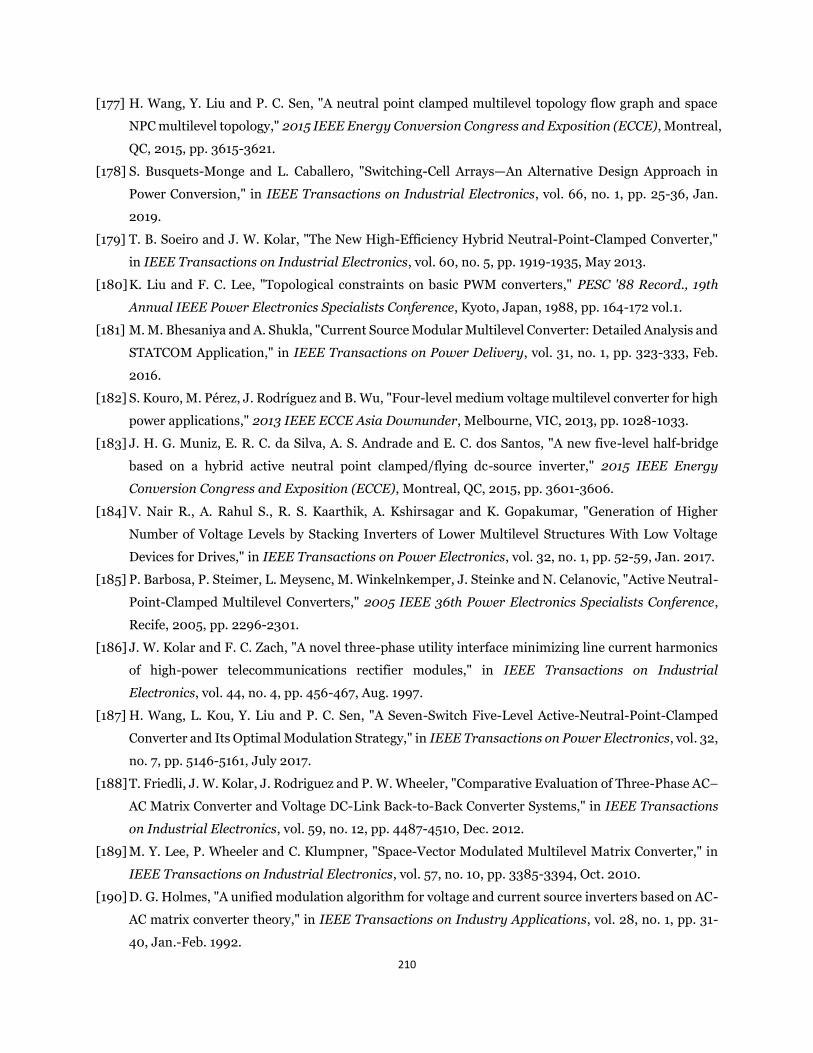
210
[177] H. Wang, Y. Liu and P. C. Sen, "A neutral point clamped multilevel topology flow graph and space
NPC multilevel topology," 2015 IEEE Energy Conversion Congress and Exposition (ECCE), Montreal,
QC, 2015, pp. 3615-3621.
[178] S. Busquets-Monge and L. Caballero, "Switching-Cell Arrays—An Alternative Design Approach in
Power Conversion," in IEEE Transactions on Industrial Electronics, vol. 66, no. 1, pp. 25-36, Jan.
2019.
[179] T. B. Soeiro and J. W. Kolar, "The New High-Efficiency Hybrid Neutral-Point-Clamped Converter,"
in IEEE Transactions on Industrial Electronics, vol. 60, no. 5, pp. 1919-1935, May 2013.
[180] K. Liu and F. C. Lee, "Topological constraints on basic PWM converters," PESC '88 Record., 19th
Annual IEEE Power Electronics Specialists Conference, Kyoto, Japan, 1988, pp. 164-172 vol.1.
[181] M. M. Bhesaniya and A. Shukla, "Current Source Modular Multilevel Converter: Detailed Analysis and
STATCOM Application," in IEEE Transactions on Power Delivery, vol. 31, no. 1, pp. 323-333, Feb.
2016.
[182] S. Kouro, M. Pérez, J. Rodríguez and B. Wu, "Four-level medium voltage multilevel converter for high
power applications," 2013 IEEE ECCE Asia Downunder, Melbourne, VIC, 2013, pp. 1028-1033.
[183] J. H. G. Muniz, E. R. C. da Silva, A. S. Andrade and E. C. dos Santos, "A new five-level half-bridge
based on a hybrid active neutral point clamped/flying dc-source inverter," 2015 IEEE Energy
Conversion Congress and Exposition (ECCE), Montreal, QC, 2015, pp. 3601-3606.
[184] V. Nair R., A. Rahul S., R. S. Kaarthik, A. Kshirsagar and K. Gopakumar, "Generation of Higher
Number of Voltage Levels by Stacking Inverters of Lower Multilevel Structures With Low Voltage
Devices for Drives," in IEEE Transactions on Power Electronics, vol. 32, no. 1, pp. 52-59, Jan. 2017.
[185] P. Barbosa, P. Steimer, L. Meysenc, M. Winkelnkemper, J. Steinke and N. Celanovic, "Active Neutral-
Point-Clamped Multilevel Converters," 2005 IEEE 36th Power Electronics Specialists Conference,
Recife, 2005, pp. 2296-2301.
[186] J. W. Kolar and F. C. Zach, "A novel three-phase utility interface minimizing line current harmonics
of high-power telecommunications rectifier modules," in IEEE Transactions on Industrial
Electronics, vol. 44, no. 4, pp. 456-467, Aug. 1997.
[187] H. Wang, L. Kou, Y. Liu and P. C. Sen, "A Seven-Switch Five-Level Active-Neutral-Point-Clamped
Converter and Its Optimal Modulation Strategy," in IEEE Transactions on Power Electronics, vol. 32,
no. 7, pp. 5146-5161, July 2017.
[188] T. Friedli, J. W. Kolar, J. Rodriguez and P. W. Wheeler, "Comparative Evaluation of Three-Phase AC–
AC Matrix Converter and Voltage DC-Link Back-to-Back Converter Systems," in IEEE Transactions
on Industrial Electronics, vol. 59, no. 12, pp. 4487-4510, Dec. 2012.
[189] M. Y. Lee, P. Wheeler and C. Klumpner, "Space-Vector Modulated Multilevel Matrix Converter," in
IEEE Transactions on Industrial Electronics, vol. 57, no. 10, pp. 3385-3394, Oct. 2010.
[190] D. G. Holmes, "A unified modulation algorithm for voltage and current source inverters based on AC-
AC matrix converter theory," in IEEE Transactions on Industry Applications, vol. 28, no. 1, pp. 31-
40, Jan.-Feb. 1992.
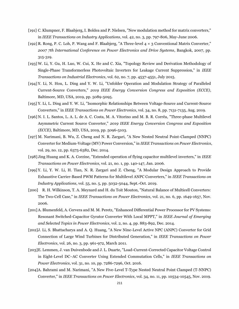
211
[191] C. Klumpner, F. Blaabjerg, I. Boldea and P. Nielsen, "New modulation method for matrix converters,"
in IEEE Transactions on Industry Applications, vol. 42, no. 3, pp. 797-806, May-June 2006.
[192] R. Rong, P. C. Loh, P. Wang and F. Blaabjerg, "A Three-level 4 × 3 Conventional Matrix Converter,"
2007 7th International Conference on Power Electronics and Drive Systems, Bangkok, 2007, pp.
315-319.
[193] W. Li, Y. Gu, H. Luo, W. Cui, X. He and C. Xia, "Topology Review and Derivation Methodology of
Single-Phase Transformerless Photovoltaic Inverters for Leakage Current Suppression," in IEEE
Transactions on Industrial Electronics, vol. 62, no. 7, pp. 4537-4551, July 2015.
[194] Y. Li, N. Hou, L. Ding and Y. W. Li, "Unfolder Operation and Modulation Strategy of Paralleled
Current-Source Converters," 2019 IEEE Energy Conversion Congress and Exposition (ECCE),
Baltimore, MD, USA, 2019, pp. 5089-5095.
[195] Y. Li, L. Ding and Y. W. Li, "Isomorphic Relationships Between Voltage-Source and Current-Source
Converters," in IEEE Transactions on Power Electronics, vol. 34, no. 8, pp. 7131-7135, Aug. 2019.
[196] N. I. L. Santos, L. A. L. de A. C. Costa, M. A. Vitorino and M. B. R. Corrêa, "Three-phase Multilevel
Asymmetric Current Source Converter," 2019 IEEE Energy Conversion Congress and Exposition
(ECCE), Baltimore, MD, USA, 2019, pp. 5096-5103.
[197] M. Narimani, B. Wu, Z. Cheng and N. R. Zargari, "A New Nested Neutral Point-Clamped (NNPC)
Converter for Medium-Voltage (MV) Power Conversion," in IEEE Transactions on Power Electronics,
vol. 29, no. 12, pp. 6375-6382, Dec. 2014.
[198] Jing Huang and K. A. Corzine, "Extended operation of flying capacitor multilevel inverters," in IEEE
Transactions on Power Electronics, vol. 21, no. 1, pp. 140-147, Jan. 2006.
[199] Y. Li, Y. W. Li, H. Tian, N. R. Zargari and Z. Cheng, "A Modular Design Approach to Provide
Exhaustive Carrier-Based PWM Patterns for Multilevel ANPC Converters," in IEEE Transactions on
Industry Applications, vol. 55, no. 5, pp. 5032-5044, Sept.-Oct. 2019.
[200] R. H. Wilkinson, T. A. Meynard and H. du Toit Mouton, "Natural Balance of Multicell Converters:
The Two-Cell Case," in IEEE Transactions on Power Electronics, vol. 21, no. 6, pp. 1649-1657, Nov.
2006.
[201] A. Blumenfeld, A. Cervera and M. M. Peretz, "Enhanced Differential Power Processor for PV Systems:
Resonant Switched-Capacitor Gyrator Converter With Local MPPT," in IEEE Journal of Emerging
and Selected Topics in Power Electronics, vol. 2, no. 4, pp. 883-892, Dec. 2014.
[202] J. Li, S. Bhattacharya and A. Q. Huang, "A New Nine-Level Active NPC (ANPC) Converter for Grid
Connection of Large Wind Turbines for Distributed Generation," in IEEE Transactions on Power
Electronics, vol. 26, no. 3, pp. 961-972, March 2011.
[203] E. Lemmen, J. van Duivenbode and J. L. Duarte, "Load-Current-Corrected Capacitor Voltage Control
in Eight-Level DC–AC Converter Using Extended Commutation Cells," in IEEE Transactions on
Power Electronics, vol. 31, no. 10, pp. 7286-7296, Oct. 2016.
[204] A. Bahrami and M. Narimani, "A New Five-Level T-Type Nested Neutral Point Clamped (T-NNPC)
Converter," in IEEE Transactions on Power Electronics, vol. 34, no. 11, pp. 10534-10545, Nov. 2019.
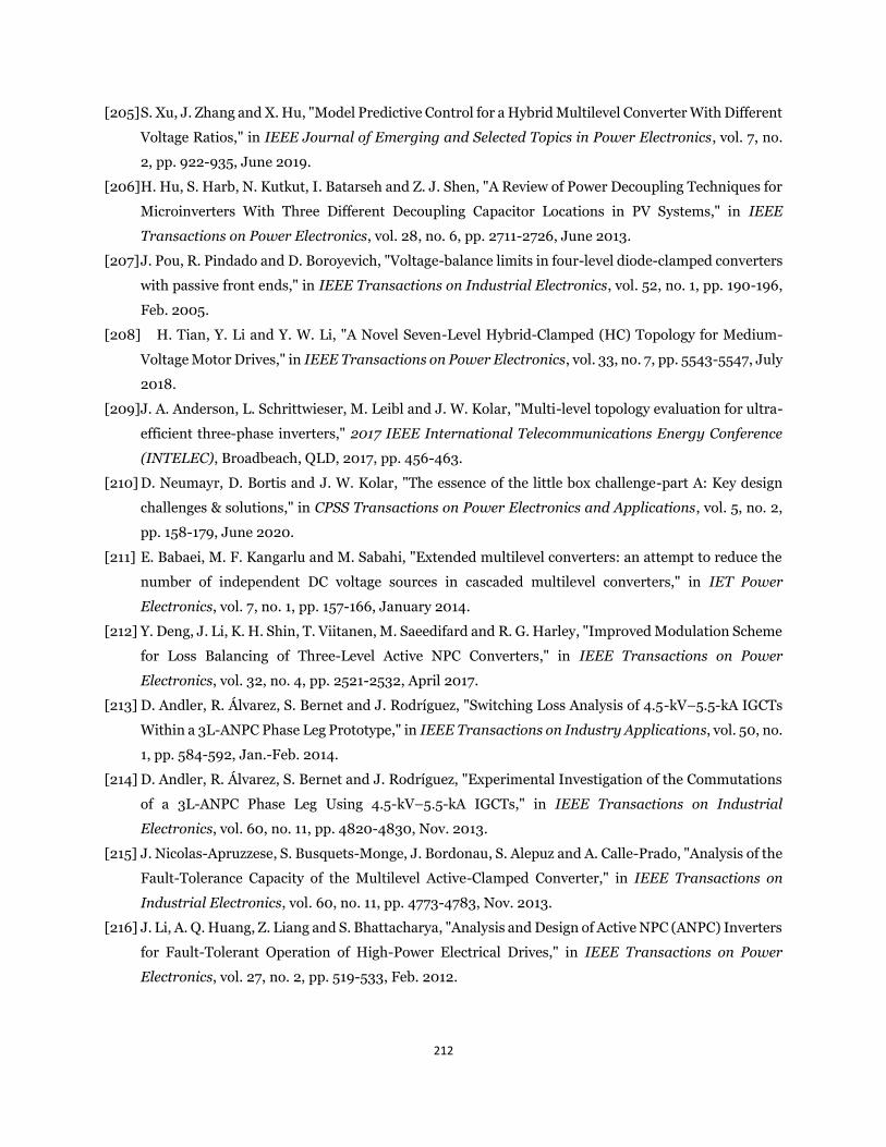
212
[205] S. Xu, J. Zhang and X. Hu, "Model Predictive Control for a Hybrid Multilevel Converter With Different
Voltage Ratios," in IEEE Journal of Emerging and Selected Topics in Power Electronics, vol. 7, no.
2, pp. 922-935, June 2019.
[206] H. Hu, S. Harb, N. Kutkut, I. Batarseh and Z. J. Shen, "A Review of Power Decoupling Techniques for
Microinverters With Three Different Decoupling Capacitor Locations in PV Systems," in IEEE
Transactions on Power Electronics, vol. 28, no. 6, pp. 2711-2726, June 2013.
[207] J. Pou, R. Pindado and D. Boroyevich, "Voltage-balance limits in four-level diode-clamped converters
with passive front ends," in IEEE Transactions on Industrial Electronics, vol. 52, no. 1, pp. 190-196,
Feb. 2005.
[208] H. Tian, Y. Li and Y. W. Li, "A Novel Seven-Level Hybrid-Clamped (HC) Topology for Medium-
Voltage Motor Drives," in IEEE Transactions on Power Electronics, vol. 33, no. 7, pp. 5543-5547, July
2018.
[209] J. A. Anderson, L. Schrittwieser, M. Leibl and J. W. Kolar, "Multi-level topology evaluation for ultra-
efficient three-phase inverters," 2017 IEEE International Telecommunications Energy Conference
(INTELEC), Broadbeach, QLD, 2017, pp. 456-463.
[210] D. Neumayr, D. Bortis and J. W. Kolar, "The essence of the little box challenge-part A: Key design
challenges & solutions," in CPSS Transactions on Power Electronics and Applications, vol. 5, no. 2,
pp. 158-179, June 2020.
[211] E. Babaei, M. F. Kangarlu and M. Sabahi, "Extended multilevel converters: an attempt to reduce the
number of independent DC voltage sources in cascaded multilevel converters," in IET Power
Electronics, vol. 7, no. 1, pp. 157-166, January 2014.
[212] Y. Deng, J. Li, K. H. Shin, T. Viitanen, M. Saeedifard and R. G. Harley, "Improved Modulation Scheme
for Loss Balancing of Three-Level Active NPC Converters," in IEEE Transactions on Power
Electronics, vol. 32, no. 4, pp. 2521-2532, April 2017.
[213] D. Andler, R. Álvarez, S. Bernet and J. Rodríguez, "Switching Loss Analysis of 4.5-kV–5.5-kA IGCTs
Within a 3L-ANPC Phase Leg Prototype," in IEEE Transactions on Industry Applications, vol. 50, no.
1, pp. 584-592, Jan.-Feb. 2014.
[214] D. Andler, R. Álvarez, S. Bernet and J. Rodríguez, "Experimental Investigation of the Commutations
of a 3L-ANPC Phase Leg Using 4.5-kV–5.5-kA IGCTs," in IEEE Transactions on Industrial
Electronics, vol. 60, no. 11, pp. 4820-4830, Nov. 2013.
[215] J. Nicolas-Apruzzese, S. Busquets-Monge, J. Bordonau, S. Alepuz and A. Calle-Prado, "Analysis of the
Fault-Tolerance Capacity of the Multilevel Active-Clamped Converter," in IEEE Transactions on
Industrial Electronics, vol. 60, no. 11, pp. 4773-4783, Nov. 2013.
[216] J. Li, A. Q. Huang, Z. Liang and S. Bhattacharya, "Analysis and Design of Active NPC (ANPC) Inverters
for Fault-Tolerant Operation of High-Power Electrical Drives," in IEEE Transactions on Power
Electronics, vol. 27, no. 2, pp. 519-533, Feb. 2012.
213
[217] E. Lupon, S. Busquets-Monge and J. Nicolas-Apruzzese, "FPGA Implementation of a PWM for a
Three-Phase DC–AC Multilevel Active-Clamped Converter," in IEEE Transactions on Industrial
Informatics, vol. 10, no. 2, pp. 1296-1306, May 2014.
[218] D. Floricau, E. Floricau and M. Dumitrescu, "Natural doubling of the apparent switching frequency
using three-level ANPC converter," 2008 International School on Nonsinusoidal Currents and
Compensation, Lagow, 2008, pp. 1-6.
[219] G. Zhang, Y. Yang, F. Iannuzzo, K. Li, F. Blaabjerg and H. Xu, "Loss distribution analysis of three-
level active neutral-point-clamped (3L-ANPC) converter with different PWM strategies," 2016 IEEE
2nd Annual Southern Power Electronics Conference (SPEC), Auckland, 2016, pp. 1-6.
[220] A. M. Y. M. Ghias, J. Pou, G. J. Capella, V. G. Agelidis, R. P. Aguilera and T. Meynard, "Single-Carrier
Phase-Disposition PWM Implementation for Multilevel Flying Capacitor Converters," in IEEE
Transactions on Power Electronics, vol. 30, no. 10, pp. 5376-5380, Oct. 2015.
[221] A. K. Sadigh, V. Dargahi and K. A. Corzine, "Analytical Determination of Conduction and Switching
Power Losses in Flying-Capacitor-Based Active Neutral-Point-Clamped Multilevel Converter," in
IEEE Transactions on Power Electronics, vol. 31, no. 8, pp. 5473-5494, Aug. 2016.
[222] K. Wang, L. Xu, Z. Zheng and Y. Li, "Capacitor Voltage Balancing of a Five-Level ANPC Converter
Using Phase-Shifted PWM," in IEEE Transactions on Power Electronics, vol. 30, no. 3, pp. 1147-1156,
March 2015.
[223] Y. Sun, Y. Liu, M. Su, W. Xiong and J. Yang, "Review of Active Power Decoupling Topologies in Single-
Phase Systems," in IEEE Transactions on Power Electronics, vol. 31, no. 7, pp. 4778-4794, July 2016,.
[224] Z. Cheng and N. Zargari, " Sparse matrix multilevel actively clamped power converter," US Patent:
US20160336872A1, 2017. (filed by Rockwell Automation Technologies Inc. in 2015)
[225] U. Choi, F. Blaabjerg and K. Lee, "Study and Handling Methods of Power IGBT Module Failures in
Power Electronic Converter Systems," in IEEE Transactions on Power Electronics, vol. 30, no. 5, pp.
2517-2533, May 2015.
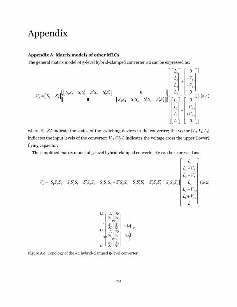
214
Appendix
Appendix A: Matrix models of other MLCs
The general matrix model of 5-level hybrid-clamped converter #2 can be expressed as:
3
3 1
2 1
21 2 1 2 1 2 1 25 5
3 4 3 4 3 4 3 4 2
2 2
1 2
1
0
0
0
0
f
f
o
f
f
LL VL VLS S S S S S S S
V S SS S S S S S S S L
L VL VL
− + +
=
− + +
00
(a-1)
where S1~S5' indicate the states of the switching devices in the converter; the vector [L3 L2 L1]
indicates the input levels of the converter; Vf 1 (Vf 2) indicates the voltage cross the upper (lower)
flying capacitor.
The simplified matrix model of 5-level hybrid-clamped converter #2 can be expressed as:
3
3 1
2 1
1 2 5 1 2 5 1 2 5 3 4 5 1 2 5 3 4 5 3 4 5 3 4 5 2
2 2
1 2
1
f
f
o
f
f
LL VL V
V S S S S S S S S S S S S S S S S S S S S S S S S LL VL V
L
− +
= + −
+
(a-2)
S'2
S2
S'4
S4
S'1
S1
S'3
S3 S'5
S5 Vo
L3
L2
L1
Vf 1
Vf 2
Figure A-1. Topology of the #2 hybrid-clamped 5-level converter.
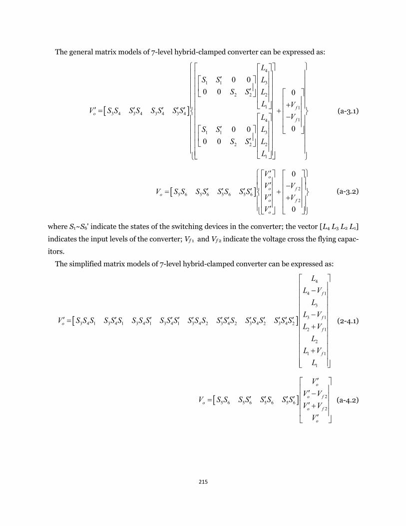
215
The general matrix models of 7-level hybrid-clamped converter can be expressed as:
4
1 1 3
2 2 2
1 13 4 3 4 3 4 3 4
14
1 1 3
2 2 2
1
0 00 0 0
00 00 0
fo
f
LS S L
S S LL V
V S S S S S S S SVL
S S LS S L
L
+ = + −
(a-3.1)
25 6 5 6 5 6 5 6
2
0
0
o
o fo
o f
o
VV V
V S S S S S S S SV VV
− = +
+
(a-3.2)
where S1~S6' indicate the states of the switching devices in the converter; the vector [L4 L3 L2 L1]
indicates the input levels of the converter; Vf 1 and Vf 2 indicate the voltage cross the flying capac-
itors.
The simplified matrix models of 7-level hybrid-clamped converter can be expressed as:
4
4 1
3
3 13 4 1 3 4 1 3 4 1 3 4 1 3 4 2 3 4 2 3 4 2 3 4 2
2 1
2
1 1
1
f
fo
f
f
LL V
LL V
V S S S S S S S S S S S S S S S S S S S S S S S SL V
LL V
L
−
− = + +
(2-4.1)
25 6 5 6 5 6 5 6
2
o
o fo
o f
o
VV V
V S S S S S S S SV V
V
− = +
(a-4.2)
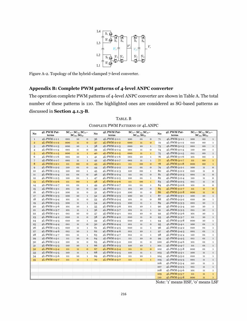
216
S'1
S1
S'2
S2S'4
S4
S'5
S5
Vo
S3
S'3
S6
S'6
L1
L2
L3
L4
Vf 1 Vf 2
V'o
Figure A-2. Topology of the hybrid-clamped 7-level converter.
Appendix B: Complete PWM patterns of 4-level ANPC converter
The operation complete PWM patterns of 4-level ANPC converter are shown in Table A. The total
number of these patterns is 110. The highlighted ones are considered as SG-based patterns as
discussed in Section 4.1.3-B.
TABLE. B
COMPLETE PWM PATTERNS OF 4L ANPC
No 4L PWM Pat-
terns SC11~ SC13, SC21~
SC22, SG31 No
4L PWM Pat-terns
SC11~ SC13, SC21~ SC22, SG31
No 4L PWM Pat-
terns SC11~ SC13, SC21~
SC22, SG31
1 4L-PWM-1-1-1 001 10 0 36 4L-PWM-2-1-1 100 01 0 71 4L-PWM-3-1-1 100 00 1
2 4L-PWM-1-1-2 000 11 0 37 4L-PWM-2-1-2 000 11 0 72 4L-PWM-3-1-2 010 00 1
3 4L-PWM-1-1-3 000 10 1 38 4L-PWM-2-1-3 000 10 1 73 4L-PWM-3-1-3 001 00 1
4 4L-PWM-1-1-4 001 11 0 39 4L-PWM-2-1-4 001 11 0 74 4L-PWM-3-1-4 110 00 1
5 4L-PWM-1-1-5 000 11 1 40 4L-PWM-2-1-5 000 11 1 75 4L-PWM-3-1-5 011 00 1
6 4L-PWM-1-1-6 001 10 1 41 4L-PWM-2-1-6 001 10 1 76 4L-PWM-3-1-6 101 00 1
7 4L-PWM-1-1-7 001 11 1 42 4L-PWM-2-1-7 001 11 1 77 4L-PWM-3-1-7 111 00 1
8 4L-PWM-1-2-1 111 00 0 43 4L-PWM-2-2-1 111 00 0 78 4L-PWM-3-1-8 000 00 1
9 4L-PWM-1-2-2 110 01 0 44 4L-PWM-2-2-2 110 01 0 79 4L-PWM-3-2-1 100 11 0
10 4L-PWM-1-2-3 110 00 1 45 4L-PWM-2-2-3 110 00 1 80 4L-PWM-3-2-2 010 11 0
11 4L-PWM-1-2-4 111 01 0 46 4L-PWM-2-2-4 111 01 0 81 4L-PWM-3-2-3 001 11 0
12 4L-PWM-1-2-5 110 01 1 47 4L-PWM-2-2-5 110 01 1 82 4L-PWM-3-2-4 110 11 0
13 4L-PWM-1-2-6 111 00 1 48 4L-PWM-2-2-6 111 00 1 83 4L-PWM-3-2-5 011 11 0
14 4L-PWM-1-2-7 111 01 1 49 4L-PWM-2-2-7 111 01 1 84 4L-PWM-3-2-6 101 11 0
15 4L-PWM-1-3-1 101 10 0 50 4L-PWM-2-3-1 101 10 0 85 4L-PWM-3-2-7 111 11 0
16 4L-PWM-1-3-2 100 11 0 51 4L-PWM-2-3-2 100 11 0 86 4L-PWM-3-2-8 000 11 0
17 4L-PWM-1-3-3 100 10 1 52 4L-PWM-2-3-3 100 10 1 87 4L-PWM-3-3-1 100 10 1
18 4L-PWM-1-3-4 101 11 0 53 4L-PWM-2-3-4 101 11 0 88 4L-PWM-3-3-2 010 10 1
19 4L-PWM-1-3-5 100 11 1 54 4L-PWM-2-3-5 100 11 1 89 4L-PWM-3-3-3 001 10 1
20 4L-PWM-1-3-6 101 10 1 55 4L-PWM-2-3-6 101 10 1 90 4L-PWM-3-3-4 110 10 1
21 4L-PWM-1-3-7 101 11 1 56 4L-PWM-2-3-7 101 11 1 91 4L-PWM-3-3-5 011 10 1
22 4L-PWM-1-4-1 011 10 0 57 4L-PWM-2-4-1 011 10 0 92 4L-PWM-3-3-6 101 10 1
23 4L-PWM-1-4-2 010 11 0 58 4L-PWM-2-4-2 010 11 0 93 4L-PWM-3-3-7 111 10 1
24 4L-PWM-1-4-3 010 10 1 59 4L-PWM-2-4-3 010 10 1 94 4L-PWM-3-3-8 000 10 1
25 4L-PWM-1-4-4 011 11 0 50 4L-PWM-2-4-4 011 11 0 95 4L-PWM-3-4-1 100 01 1
26 4L-PWM-1-4-5 010 11 1 61 4L-PWM-2-4-5 010 11 1 96 4L-PWM-3-4-2 010 01 1
27 4L-PWM-1-4-6 011 10 1 62 4L-PWM-2-4-6 011 10 1 97 4L-PWM-3-4-3 001 01 1
28 4L-PWM-1-4-7 011 11 1 63 4L-PWM-2-4-7 011 11 1 98 4L-PWM-3-4-4 110 01 1
29 4L-PWM-1-5-1 111 10 0 64 4L-PWM-2-5-1 111 10 0 99 4L-PWM-3-4-5 011 01 1
30 4L-PWM-1-5-2 110 11 0 65 4L-PWM-2-5-2 110 11 0 100 4L-PWM-3-4-6 101 01 1
31 4L-PWM-1-5-3 110 10 1 66 4L-PWM-2-5-3 110 10 1 101 4L-PWM-3-4-7 111 01 1
32 4L-PWM-1-5-4 111 11 0 67 4L-PWM-2-5-4 111 11 0 102 4L-PWM-3-5-8 000 01 1
33 4L-PWM-1-5-5 110 11 1 68 4L-PWM-2-5-5 110 11 1 103 4L-PWM-3-5-1 100 11 1
34 4L-PWM-1-5-6 111 10 1 69 4L-PWM-2-5-6 111 10 1 104 4L-PWM-3-5-2 010 11 1
35 4L-PWM-1-5-7 111 11 1 70 4L-PWM-2-5-7 111 11 1 105 4L-PWM-3-5-3 001 11 1
106 4L-PWM-3-5-4 110 11 1
107 4L-PWM-3-5-5 011 11 1
108 4L-PWM-3-5-6 101 11 1
109 4L-PWM-3-5-7 111 11 1
110 4L-PWM-3-5-8 000 11 1
Note: ‘1’ means HSF, ‘0’ means LSF
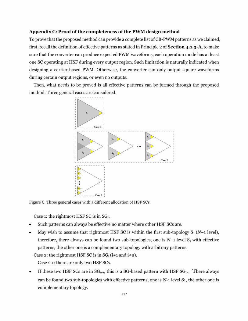
217
Appendix C: Proof of the completeness of the PWM design method
To prove that the proposed method can provide a complete list of CB-PWM patterns as we claimed,
first, recall the definition of effective patterns as stated in Principle 2 of Section 4.1.3-A, to make
sure that the converter can produce expected PWM waveforms, each operation mode has at least
one SC operating at HSF during every output region. Such limitation is naturally indicated when
designing a carrier-based PWM. Otherwise, the converter can only output square waveforms
during certain output regions, or even no outputs.
Then, what needs to be proved is all effective patterns can be formed through the proposed
method. Three general cases are considered.
S1S1S1S1
S2S2
S1
S2S2
S1
S3
S1
Sn
Sn-1
S3
S2
S1
Case 1
Case 3
Case 2
Figure C. Three general cases with a different allocation of HSF SCs.
Case 1: the rightmost HSF SC is in SGn.
• Such patterns can always be effective no matter where other HSF SCs are.
• May wish to assume that rightmost HSF SC is within the first sub-topology S1 (N−1 level),
therefore, there always can be found two sub-topologies, one is N−1 level S1 with effective
patterns, the other one is a complementary topology with arbitrary patterns.
Case 2: the rightmost HSF SC is in SGi (i≠1 and i≠n).
Case 2.1: there are only two HSF SCs.
• If these two HSF SCs are in SGn-1, this is a SG-based pattern with HSF SGn-1. There always
can be found two sub-topologies with effective patterns, one is N-1 level S1, the other one is
complementary topology.
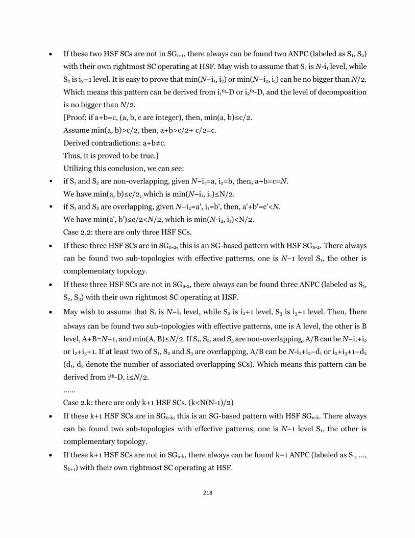
218
• If these two HSF SCs are not in SGn-1, there always can be found two ANPC (labeled as S1, S2)
with their own rightmost SC operating at HSF. May wish to assume that S1 is N-i1 level, while
S2 is i2+1 level. It is easy to prove that min(N−i1, i2) or min(N−i2, i1) can be no bigger than N/2.
Which means this pattern can be derived from i1th-D or i2
th-D, and the level of decomposition
is no bigger than N/2.
[Proof: if a+b=c, (a, b, c are integer), then, min(a, b)≤c/2.
Assume min(a, b)>c/2, then, a+b>c/2+ c/2=c.
Derived contradictions: a+b≠c.
Thus, it is proved to be true.]
Utilizing this conclusion, we can see:
▪ if S1 and S2 are non-overlapping, given N−i1=a, i2=b, then, a+b=c=N.
We have min(a, b)≤c/2, which is min(N−i1, i2)≤N/2.
▪ if S1 and S2 are overlapping, given N−i2=a', i1=b', then, a'+b'=c'<N.
We have min(a', b')≤c/2<N/2, which is min(N-i2, i1)<N/2.
Case 2.2: there are only three HSF SCs.
• If these three HSF SCs are in SGn-2, this is an SG-based pattern with HSF SGn-2. There always
can be found two sub-topologies with effective patterns, one is N−1 level S1, the other is
complementary topology.
• If these three HSF SCs are not in SGn-2, there always can be found three ANPC (labeled as S1,
S2, S3) with their own rightmost SC operating at HSF.
• May wish to assume that S1 is N−i1 level, while S2 is i2+1 level, S3 is i3+1 level. Then, there
always can be found two sub-topologies with effective patterns, one is A level, the other is B
level, A+B=N−1, and min(A, B)≤N/2. If S1, S2, and S3 are non-overlapping, A/B can be N−i1+i2
or i2+i3+1. If at least two of S1, S2 and S3 are overlapping, A/B can be N-i1+i2−d1 or i2+i3+1−d2
(d1, d2 denote the number of associated overlapping SCs). Which means this pattern can be
derived from ith-D, i≤N/2.
……
Case 2.k: there are only k+1 HSF SCs. (k<N(N-1)/2)
• If these k+1 HSF SCs are in SGn-k, this is an SG-based pattern with HSF SGn-k. There always
can be found two sub-topologies with effective patterns, one is N−1 level S1, the other is
complementary topology.
• If these k+1 HSF SCs are not in SGn-k, there always can be found k+1 ANPC (labeled as S1, …,
Sk+1) with their own rightmost SC operating at HSF.
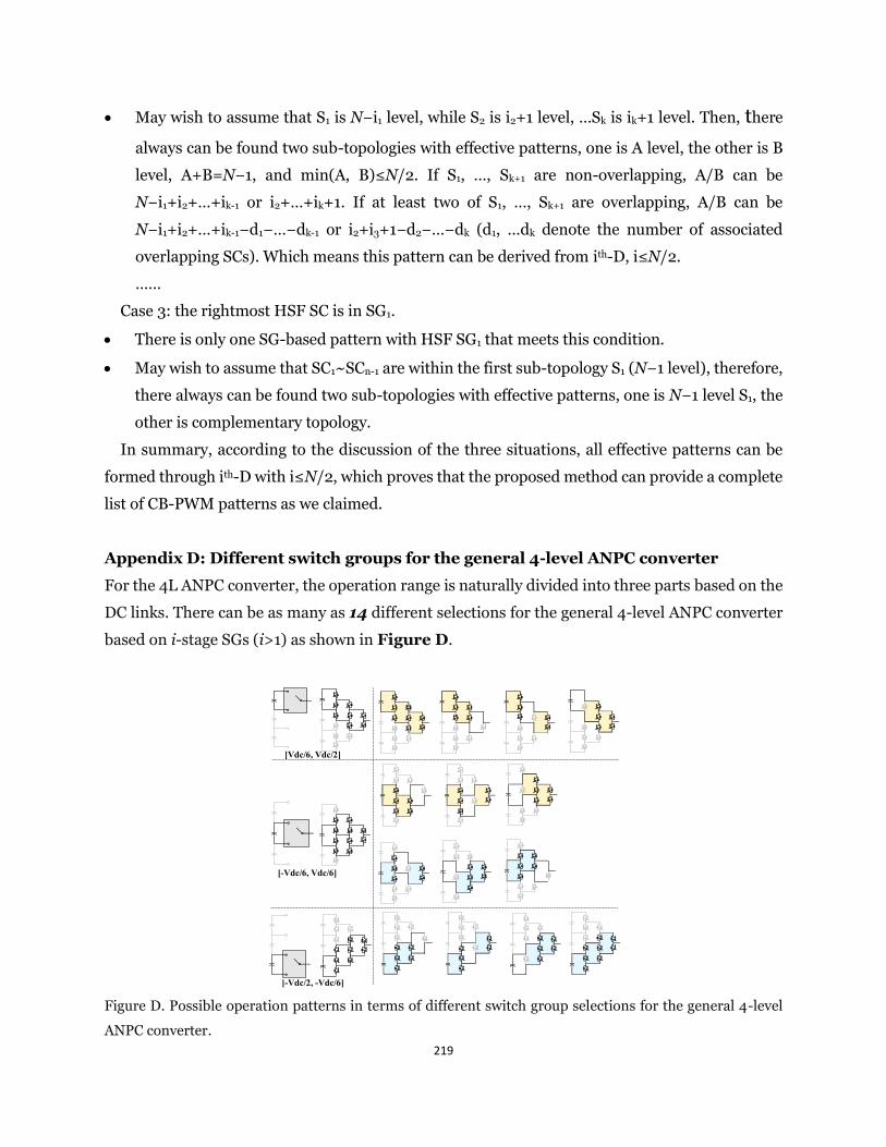
219
• May wish to assume that S1 is N−i1 level, while S2 is i2+1 level, …Sk is ik+1 level. Then, there
always can be found two sub-topologies with effective patterns, one is A level, the other is B
level, A+B=N−1, and min(A, B)≤N/2. If S1, …, Sk+1 are non-overlapping, A/B can be
N−i1+i2+…+ik-1 or i2+…+ik+1. If at least two of S1, …, Sk+1 are overlapping, A/B can be
N−i1+i2+…+ik-1−d1−…−dk-1 or i2+i3+1−d2−…−dk (d1, …dk denote the number of associated
overlapping SCs). Which means this pattern can be derived from ith-D, i≤N/2.
……
Case 3: the rightmost HSF SC is in SG1.
• There is only one SG-based pattern with HSF SG1 that meets this condition.
• May wish to assume that SC1~SCn-1 are within the first sub-topology S1 (N−1 level), therefore,
there always can be found two sub-topologies with effective patterns, one is N−1 level S1, the
other is complementary topology.
In summary, according to the discussion of the three situations, all effective patterns can be
formed through ith-D with i≤N/2, which proves that the proposed method can provide a complete
list of CB-PWM patterns as we claimed.
Appendix D: Different switch groups for the general 4-level ANPC converter
For the 4L ANPC converter, the operation range is naturally divided into three parts based on the
DC links. There can be as many as 14 different selections for the general 4-level ANPC converter
based on i-stage SGs (i>1) as shown in Figure D.
[Vdc/6, Vdc/2]
[-Vdc/6, Vdc/6]
[-Vdc/2, -Vdc/6]
Figure D. Possible operation patterns in terms of different switch group selections for the general 4-level
ANPC converter.
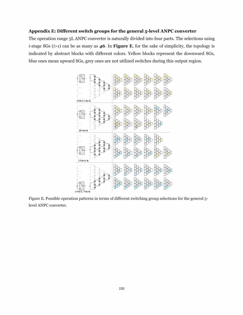
220
Appendix E: Different switch groups for the general 5-level ANPC converter
The operation range 5L ANPC converter is naturally divided into four parts. The selections using
i-stage SGs (i>1) can be as many as 46. In Figure E, for the sake of simplicity, the topology is
indicated by abstract blocks with different colors. Yellow blocks represent the downward SGs,
blue ones mean upward SGs, grey ones are not utilized switches during this output region.
[Vdc/4, Vdc/2]
[0,Vdc/4]
[-Vdc/2, -Vdc/4]
[-Vdc/4, 0]
Figure E. Possible operation patterns in terms of different switching group selections for the general 5-
level ANPC converter.