Embed Size (px)
Citation preview
USER’S MANUAL
Revision 1.2
X8STi-FX8STi-3F
X8STi
X8STi-LN4

Manual Revision 1.2
Release Date: February 23, 2012
Unless you request and receive written permission from Super Micro Computer, Inc., you may not copy any part of this document. Information in this document is subject to change without notice. Other products and companies referred to herein are trademarks or registered trademarks of their respective companies or mark holders.
Copyright © 2012 by Super Micro Computer, Inc. All rights reserved. Printed in the United States of America
The information in this User’s Manual has been carefully reviewed and is believed to be accurate. The vendor assumes no responsibility for any inaccuracies that may be contained in this document, makes no commitment to update or to keep current the information in this manual, or to notify any person or organization of the updates. Please Note: For the most up-to-date version of this manual, please see our web site at www.supermicro.com.
Super Micro Computer, Inc. ("Supermicro") reserves the right to make changes to the product described in this manual at any time and without notice. This product, including software and docu-mentation, is the property of Supermicro and/or its licensors, and is supplied only under a license. Any use or reproduction of this product is not allowed, except as expressly permitted by the terms of said license.
IN NO EVENT WILL SUPER MICRO COMPUTER, INC. BE LIABLE FOR DIRECT, INDIRECT, SPECIAL, INCIDENTAL, SPECULATIVE OR CONSEQUENTIAL DAMAGES ARISING FROM THE USE OR INABILITY TO USE THIS PRODUCT OR DOCUMENTATION, EVEN IF ADVISED OF THE POSSIBILITY OF SUCH DAMAGES. IN PARTICULAR, SUPER MICRO COMPUTER, INC. SHALL NOT HAVE LIABILITY FOR ANY HARDWARE, SOFTWARE, OR DATA STORED OR USED WITH THE PRODUCT, INCLUDING THE COSTS OF REPAIRING, REPLACING, INTEGRATING, INSTALLING OR RECOVERING SUCH HARDWARE, SOFTWARE, OR DATA.
Any disputes arising between manufacturer and customer shall be governed by the laws of Santa Clara County in the State of California, USA. The State of California, County of Santa Clara shall be the exclusive venue for the resolution of any such disputes. Supermicro's total liability for all claims will not exceed the price paid for the hardware product.
FCC Statement: This equipment has been tested and found to comply with the limits for a Class B digital device pursuant to Part 15 of the FCC Rules. These limits are designed to provide reason-able protection against harmful interference in a residential installation. This equipment generates, uses, and can radiate radio frequency energy and, if not installed and used in accordance with the manufacturer’s instruction manual, may cause interference with radio communications. However, there is no guarantee that interference will not occur in a particular installation. If this equipment does cause harmful interference to radio or television reception, which can be determined by turn-ing the equipment off and on, you are encouraged to try to correct the interference by one or more of the following measures:
•Reorient or relocate the receiving antenna.•Increase the separation between the equipment and the receiver.•Connect the equipment into an outlet on a circuit different from that to which the
receiver is connected.•Consult the dealer or an experienced radio/television technician for help.
California Best Management Practices Regulations for Perchlorate Materials: This Perchlorate warn-ing applies only to products containing CR (Manganese Dioxide) Lithium coin cells. “Perchlorate Material-special handling may apply. See www.dtsc.ca.gov/hazardouswaste/perchlorate”.
WARNING: Handling of lead solder materials used in this product may expose you to lead, a chemical known to the State of California to cause birth defects and other reproductive harm.
Preface
This manual is writ ten for system integrators, PC technicians and knowledgeable PC users. It provides information for the installation and use of the
X8STi/X8STi-F/X8STi-3F/X8STi-LN4 motherboard.
About This Motherboard
The X8STi/X8STi-F/X8STi-3F/X8STi-LN4 supports the Intel® Core™ i7 processor and Intel® Xeon® 5500/3500 series processors in an LGA 1366 socket. These processors support the Intel QuickPath Interconnect (QPI) technology, provid-ing the next generation point-to-point system interface which replaces the current Front Side Bus. With the Intel X58 Express chipset built-in, the X8STi/X8STi-F/X8STi-3F/X8STi-LN4 offers substantial enhancement in system performance with in-creased bandwidth and unprecedented scalability, optimized for intense-computing and high-end server platforms. Please refer to our web site (http://www.supermicro.com/products/) for updates on supported processors. This product is intended to be installed and serviced by professional technicians.
Manual Organization
Chapter 1describes the features,specificationsandperformanceof themother-board and provides detailed information about the chipset.
Chapter 2 provides hardware installation instructions. Read this chapter when in-stalling the processor, memory modules and other hardware components into the system. If you encounter any problems, see Chapter 3, which describes trouble-shooting procedures for video, memory and system setup stored in the CMOS.
Chapter 4 includes an introduction to the BIOS and provides detailed information on running the CMOS Setup utility.
Appendix A provides BIOS Error Beep Codes.
Appendix B lists the Windows OS Installation Instructions.
Appendix C and Appendix D lists Other Software Program Installation Instructions and BIOS Recovery Instructions.
Preface
iii

X8STi/X8STi-F/X8STi-3F/X8STi-LN4 User’s Manual
Conventions Used in the Manual:
Special attention should be given to the following symbols for proper installation and to prevent damage done to the components or injury to yourself:
Danger/Caution: Instructions to be strictly followed to prevent catastrophic system failure or to avoid bodily injury
Warning: Important information given to ensure proper system installation or to prevent damage to the components
Note: Additional Information given to differentiate various models or pro-vides information for correct system setup.
iv
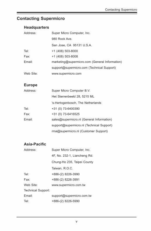
Contacting Supermicro
v
Contacting Supermicro
HeadquartersAddress: Super Micro Computer, Inc.
980 Rock Ave.
San Jose, CA 95131 U.S.A.
Tel: +1 (408) 503-8000
Fax: +1 (408) 503-8008
Email: [email protected] (General Information)
[email protected] (Technical Support)
Web Site: www.supermicro.com
EuropeAddress: Super Micro Computer B.V.
Het Sterrenbeeld 28, 5215 ML
's-Hertogenbosch, The Netherlands
Tel: +31 (0) 73-6400390
Fax: +31 (0) 73-6416525
Email: [email protected] (General Information)
[email protected] (Technical Support)
[email protected] (Customer Support)
Asia-PacificAddress: Super Micro Computer, Inc.
4F, No. 232-1, Liancheng Rd.
Chung-Ho 235, Taipei County
Taiwan, R.O.C.
Tel: +886-(2) 8226-3990
Fax: +886-(2) 8226-3991
Web Site: www.supermicro.com.tw
Technical Support:
Email: [email protected]
Tel: +886-(2) 8226-5990
vi
X8STi/X8STi-F/X8STi-3F/X8STi-LN4 User’s Manual
Table of Contents
PrefaceAbout This Motherboard ................................................................................................ 3Manual Organization ..................................................................................................... 3Conventions Used in the Manual: ................................................................................. 4Contacting Supermicro .................................................................................................. 5
Chapter 1 Introduction1-1 Overview ......................................................................................................... 1-1
Checklist .......................................................................................................... 1-1Motherboard Features ..................................................................................... 1-7
1-2 Chipset Overview ..........................................................................................1-11Features of the LGA 1366 Processor and the X58 Chipset ..........................1-11
1-3 PC Health Monitoring .................................................................................... 1-12Recovery from AC Power Loss ..................................................................... 1-12Onboard Voltage Monitoring ........................................................................ 1-12Fan Status Monitor with Software ................................................................. 1-12CPU Overheat LED and Control .................................................................. 1-12
1-4 PowerConfigurationSettings........................................................................ 1-12Slow Blinking LED for Suspend-State Indicator ........................................... 1-13BIOS Support for USB Keyboard.................................................................. 1-13Main Switch Override Mechanism ................................................................ 1-13Wake-On-LAN (WOL) ................................................................................... 1-13
1-5 Power Supply ................................................................................................ 1-131-6 Super I/O ....................................................................................................... 1-141-7 Overview of the Winbond WPCM450 Controller .......................................... 1-14
Chapter 2 Installation2-1 Static-Sensitive Devices .................................................................................. 2-1
Precautions ..................................................................................................... 2-1Unpacking ....................................................................................................... 2-1
2-2 Processor and Heatsink Installation................................................................ 2-2Installing an LGA 1366 Processor .................................................................. 2-2Installing a Passive CPU Heatsink (#SNK-P0037) ......................................... 2-4Removing the Heatsink ................................................................................... 2-5
2-3 Mounting the Motherboard into the Chassis ................................................... 2-62-4 Installing and Removing the Memory Modules ............................................... 2-7
Installing & Removing DIMMs ......................................................................... 2-72-5 Connectors/IO Ports ...................................................................................... 2-10
vii
Table of Contents
Back Panel Connectors and IO Ports ........................................................... 2-10ATX PS/2 Keyboard and PS/2 Mouse Ports .............................................2-11Universal Serial Bus (USB) ...................................................................... 2-12Ethernet Ports .......................................................................................... 2-13Serial Ports ............................................................................................... 2-14Video Connector ....................................................................................... 2-15
Front Control Panel ....................................................................................... 2-16FrontControlPanelPinDefinitions............................................................... 2-17
NMI Button ............................................................................................... 2-17Power LED .............................................................................................. 2-17HDD LED/UID Switch ............................................................................... 2-18NIC1/NIC2/NIC3*/NIC4* LEDs (*NIC3/NIC4: X8STi-LN4) ....................... 2-18Overheat (OH)/Fan Fail/Blue UID LED .................................................... 2-19Power Fail LED ........................................................................................ 2-19Reset Button ........................................................................................... 2-20Power Button ........................................................................................... 2-20
2-6 Connecting Cables ........................................................................................ 2-21ATX Main PWR & CPU PWR Connectors .............................................. 2-21Fan Headers ............................................................................................. 2-22Chassis Intrusion ..................................................................................... 2-22Internal Buzzer ......................................................................................... 2-23Speaker .................................................................................................... 2-23Overheat/Fan Fail LED ............................................................................ 2-24NIC3_LED/NIC4_LED (X8STi-LN4 Only) ................................................. 2-24Onboard Power LED ................................................................................ 2-25Power Supply I2C Connector.................................................................... 2-25T-SGPIO 0/1 & 3-SGPIO 0/1 Headers ..................................................... 2-26Alarm Reset .............................................................................................. 2-26Wake-On-LAN .......................................................................................... 2-27I-Button (X8STi-3F only) ........................................................................... 2-27Power Supply Failure ............................................................................... 2-28UnitIdentifierSwitches ............................................................................. 2-28
2-7 Jumper Settings ............................................................................................ 2-29Explanation of Jumpers ................................................................................ 2-29
LAN Port Enable/Disable ......................................................................... 2-29CMOS Clear ............................................................................................. 2-30Watch Dog Enable/Disable ...................................................................... 2-30PCI Slot_SMB Enable .............................................................................. 2-31VGA Enable .............................................................................................. 2-31
viii
USB Wake-Up ......................................................................................... 2-32SAS Enable/Disable (X8STi-3F Only) ...................................................... 2-33SAS RAID Mode Select (X8STi-3F Only) ................................................ 2-33JBMC1 (X8STi-F/X8STi-3F Only) ............................................................. 2-34
2-8 Onboard Indicators ........................................................................................ 2-35LAN 1/LAN 2 LEDs .................................................................................. 2-35IPMI Dedicated LAN LEDs (X8STi-F/X8STi-3F Only).............................. 2-35SAS Activity LED (X8STi-3F Only) ........................................................... 2-36SAS Heartbeat LED (X8STi-3F Only) ...................................................... 2-36Onboard Power LED ............................................................................................................ 2-37
BMC Heartbeat LED ................................................................................ 2-37UID-LED .................................................................................................. 2-38
2-9 SATA/SAS and Floppy Drive Connections.................................................... 2-39SATA/SAS Connections (SAS: for X8STi-3F only) .................................. 2-39Floppy Connector ..................................................................................... 2-40
Chapter 3 Troubleshooting3-1 Troubleshooting Procedures ........................................................................... 3-13-2 Technical Support Procedures ........................................................................ 3-23-3 Frequently Asked Questions ........................................................................... 3-33-4 Returning Merchandise for Service................................................................. 3-4
Chapter 4 BIOS 4-1 Introduction ...................................................................................................... 4-14-2 Main Setup ...................................................................................................... 4-24-3 AdvancedSetupConfigurations...................................................................... 4-44-4 Security Settings ........................................................................................... 4-234-5 BootConfiguration ........................................................................................ 4-24
4-6 Exit Options ................................................................................................... 4-25
Appendix A POST Error Beep CodesRecoverable POST Error Beep Codes ......................................................................A-1
Appendix B Installing the Windows OSB-1 Installing the Windows OS to a RAID System ................................................B-1B-2 Installing the Windows OS to a Non-RAID System ........................................B-2
Appendix C Software Installation InstructionsC-1 Installing Drivers ..............................................................................................C-1C-2 ConfiguringSuperoDoctorIII .........................................................................C-2
Appendix D - BIOS RecoveryD-1 Recovery Process from a USB Device/Drive (Recommended Method) .............D-1D-2 Recovery Process from an IDE/SATA ATAPI Disc Drive ....................................D-2
X8STi/X8STi-F/X8STi-3F/X8STi-LN4 User’s Manual
Chapter 1: Introduction
1-1
Chapter 1
Introduction
1-1 Overview
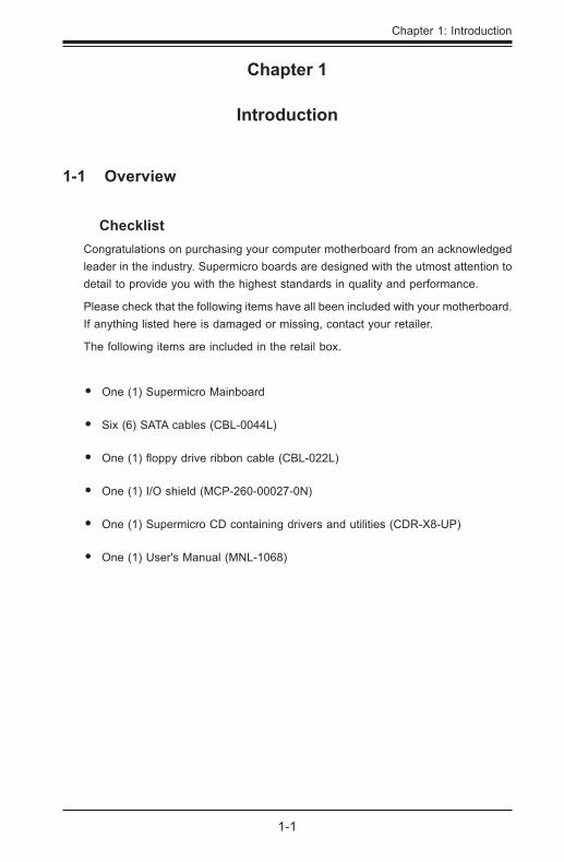
ChecklistCongratulations on purchasing your computer motherboard from an acknowledged leader in the industry. Supermicro boards are designed with the utmost attention to detail to provide you with the highest standards in quality and performance.
Please check that the following items have all been included with your motherboard. If anything listed here is damaged or missing, contact your retailer.
The following items are included in the retail box.
•One (1) Supermicro Mainboard
•Six (6) SATA cables (CBL-0044L)
•One(1)floppydriveribboncable(CBL-022L)
•One (1) I/O shield (MCP-260-00027-0N)
•One (1) Supermicro CD containing drivers and utilities (CDR-X8-UP)
•One (1) User's Manual (MNL-1068)
1-2
X8STi/X8STi-F/X8STi-3F/X8STi-LN4 User’s Manual
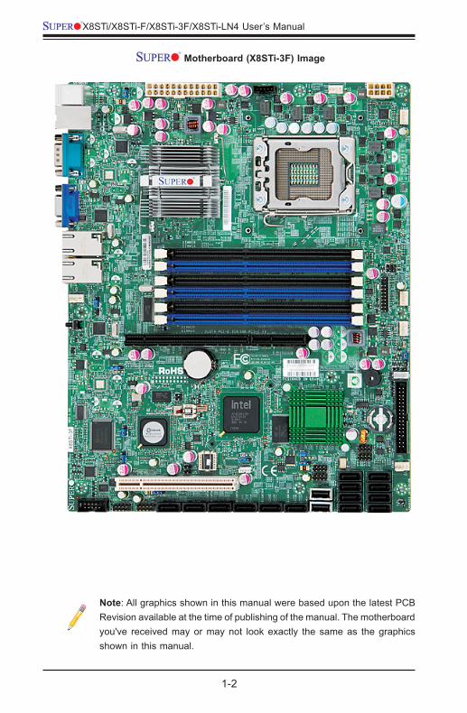
Motherboard (X8STi-3F) Image
Note: All graphics shown in this manual were based upon the latest PCB Revision available at the time of publishing of the manual. The motherboard you've received may or may not look exactly the same as the graphics shown in this manual.
Chapter 1: Introduction
1-3
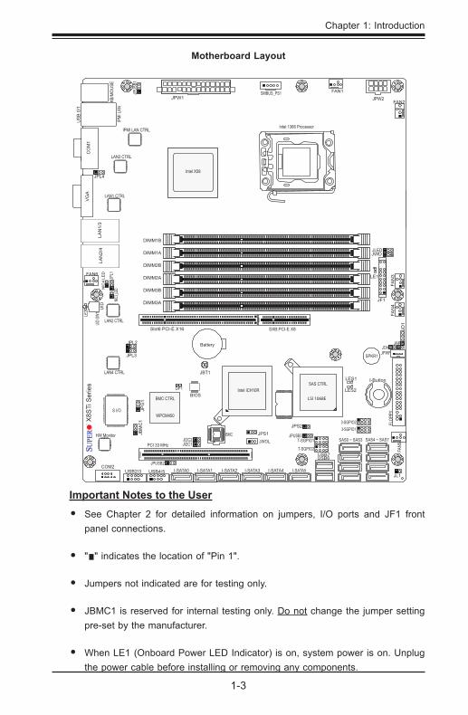
Motherboard Layout
Important Notes to the User
•See Chapter 2 for detailed information on jumpers, I/O ports and JF1 front panel connections.
•" " indicates the location of "Pin 1".
•Jumpers not indicated are for testing only.
•JBMC1 is reserved for internal testing only. Do not change the jumper setting pre-set by the manufacturer.
•When LE1 (Onboard Power LED Indicator) is on, system power is on. Unplug the power cable before installing or removing any components.
LSI 1068E
NIC
4 LE
D
JBM
C1
1-4
X8STi/X8STi-F/X8STi-3F/X8STi-LN4 User’s Manual
LSI 1068E
NIC
4 LE
D
JBM
C1
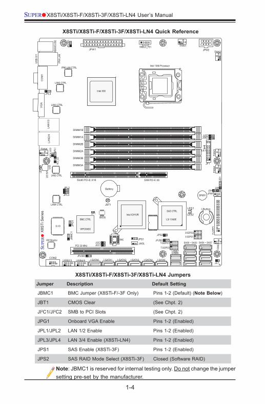
X8STi/X8STi-F/X8STi-3F/X8STi-LN4 Quick Reference
X8STi/X8STi-F/X8STi-3F/X8STi-LN4 JumpersJumper Description Default Setting
JBMC1 BMC Jumper (X8STi-F/-3F Only) Pins 1-2 (Default) (Note Below)
JBT1 CMOS Clear (See Chpt. 2)
JI2C1/JI2C2 SMB to PCI Slots (See Chpt. 2)
JPG1 Onboard VGA Enable Pins 1-2 (Enabled)
JPL1/JPL2 LAN 1/2 Enable Pins 1-2 (Enabled)
JPL3/JPL4 LAN 3/4 Enable (X8STi-LN4) Pins 1-2 (Enabled)
JPS1 SAS Enable (X8STi-3F) Pins 1-2 (Enabled)
JPS2 SAS RAID Mode Select (X8STi-3F) Closed (Software RAID)
Note: JBMC1 is reserved for internal testing only. Do not change the jumper setting pre-set by the manufacturer.
Chapter 1: Introduction
1-5
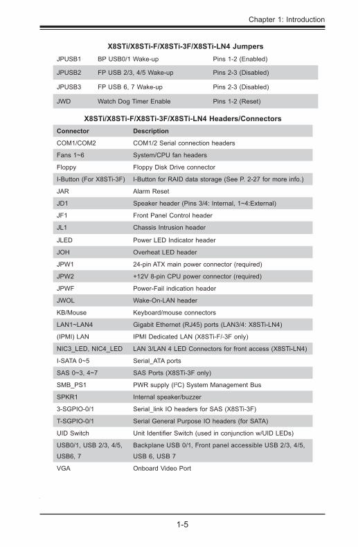
X8STi/X8STi-F/X8STi-3F/X8STi-LN4 JumpersJPUSB1 BP USB0/1 Wake-up Pins 1-2 (Enabled)
JPUSB2 FP USB 2/3, 4/5 Wake-up Pins 2-3 (Disabled)
JPUSB3 FP USB 6, 7 Wake-up Pins 2-3 (Disabled)
JWD Watch Dog Timer Enable Pins 1-2 (Reset)
X8STi/X8STi-F/X8STi-3F/X8STi-LN4 Headers/ConnectorsConnector Description
COM1/COM2 COM1/2 Serial connection headers
Fans 1~6 System/CPU fan headers
Floppy Floppy Disk Drive connector
I-Button (For X8STi-3F) I-Button for RAID data storage (See P. 2-27 for more info.)
JAR Alarm Reset
JD1 Speaker header (Pins 3/4: Internal, 1~4:External)
JF1 Front Panel Control header
JL1 Chassis Intrusion header
JLED Power LED Indicator header
JOH Overheat LED header
JPW1 24-pin ATX main power connector (required)
JPW2 +12V 8-pin CPU power connector (required)
JPWF Power-Fail indication header
JWOL Wake-On-LAN header
KB/Mouse Keyboard/mouse connectors
LAN1~LAN4 Gigabit Ethernet (RJ45) ports (LAN3/4: X8STi-LN4)
(IPMI) LAN IPMI Dedicated LAN (X8STi-F/-3F only)
NIC3_LED, NIC4_LED LAN 3/LAN 4 LED Connectors for front access (X8STi-LN4)
I-SATA 0~5 Serial_ATA ports
SAS 0~3, 4~7 SAS Ports (X8STi-3F only)
SMB_PS1 PWR supply (I2C) System Management Bus
SPKR1 Internal speaker/buzzer
3-SGPIO-0/1 Serial_link IO headers for SAS (X8STi-3F)
T-SGPIO-0/1 Serial General Purpose IO headers (for SATA)
UID Switch UnitIdentifierSwitch(usedinconjunctionw/UIDLEDs)
USB0/1, USB 2/3, 4/5,
USB6, 7
Backplane USB 0/1, Front panel accessible USB 2/3, 4/5,
USB 6, USB 7
VGA Onboard Video Port
1-6
X8STi/X8STi-F/X8STi-3F/X8STi-LN4 User’s Manual
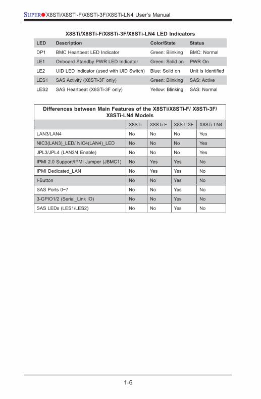
X8STi/X8STi-F/X8STi-3F/X8STi-LN4 LED IndicatorsLED Description Color/State Status
DP1 BMC Heartbeat LED Indicator Green: Blinking BMC: Normal
LE1 Onboard Standby PWR LED Indicator Green: Solid on PWR On
LE2 UID LED Indicator (used with UID Switch) Blue: Solid on UnitisIdentified
LES1 SAS Activity (X8STi-3F only) Green: Blinking SAS: Active
LES2 SAS Heartbeat (X8STi-3F only) Yellow: Blinking SAS: Normal
Differences between Main Features of the X8STi/X8STi-F/ X8STi-3F/ X8STi-LN4 Models
X8STi X8STi-F X8STi-3F X8STi-LN4
LAN3/LAN4 No No No Yes
NIC3(LAN3)_LED/ NIC4(LAN4)_LED No No No Yes
JPL3/JPL4 (LAN3/4 Enable) No No No Yes
IPMI 2.0 Support/IPMI Jumper (JBMC1) No Yes Yes No
IPMI Dedicated_LAN No Yes Yes No
I-Button No No Yes No
SAS Ports 0~7 No No Yes No
3-GPIO1/2 (Serial_Link IO) No No Yes No
SAS LEDs (LES1/LES2) No No Yes No
Chapter 1: Introduction
1-7
Motherboard Features
CPU
• Single Intel® Core™ i7 and and Intel® Xeon® 5500/3500 series processors in an LGA1366 socket.
Memory
• Six 240-pin, DDR3 SDRAM DIMM sockets with support for unbuffered ECC or non ECC 1333/1066/800 MHz memory.
Note: Both Unbuffered ECC and Non-ECC DIMM modules are supported by the motherboard. Using ECC or Non-ECC memory on your motherboard depends on the CPU installed. Please see Page 3-3 for more information on memory support.
• Supports 3-channel memory bus
• Supports DIMM sizes of 256 MB, 512 MB, 1 GB, 2 GB, and 4 GB
Chipset
• Intel® X58 Express Chipset
• Intel ICH10R
Expansion Slots
•One (1) (PCI-Express x16 Gen2 + PCI-Express x8 in x4) slot
•One (1) 32-bit PCI 33MHz slot (Slot 1)
Integrated Graphics
•Matrox G200ew with 8 MB Video Memory
Network Connections
• Two Intel 82574L Gigabit (10/100/1000 Mb/s) Ethernet Controllers for LAN 1 and LAN 2 ports, additional two 82574L for LAN 3 and LAN 4 ports on the X8STi-LN4 model
• Two (2) or four (4)* RJ-45 Rear IO Panel Connectors with Link and Activity LEDs (*Four RJ-45 ports are available on the X8STi-LN4 only)
• Single Realtek RTL8201N PHY for the Dedicated IPMI 2.0LAN for the X8STi-F/-3F
•One (1) RJ45 Rear I/O Panel Dedicated IPMI 2.0 Connector for the X8STi-F/-3F
• I/O Devices
SATA Connections
• Six (6) SATA ports supported by the Intel ICH10R SATA Controller• Supports RAID 0, 1, 5, 10 under the Windows OS environment
1-8
X8STi/X8STi-F/X8STi-3F/X8STi-LN4 User’s Manual
• Supports RAID 0, 1, 10 under the Linux OS environment
SAS Connections (for the X8STi-3F only)
• Eight (8) SAS ports supported by the LSI 1068E Controller**• Supports RAID 0, 1, 5*, 10 under the Windows OS environment • Supports RAID 0, 1, 5*, 10 under the Linux OS environment
*RAID 5 is supported when the I-Button (AOC-IButton68) is installed on the motherboard. (I-Button is available on the X8STi-3F only) For more information on the AOC-IButton68, please refer to http://www.supermicro.com/products/accessories/addon/AOC-IButton68.cfm.
**For the LSI 1068 Controller User's Guide, please refer to http://www.supermicro.com/support/manuals/.
Integrated IPMI 2.0 (for the X8STi-F/X8STi-3F only)
• IPMI 2.0 supported by the WPCM450 Server BMCNote:ForIPMIConfigurationInstructions,pleaserefertotheEmbeddedIPMIConfigurationUser'sGuideavailable@http://www.supermicro.com/support/manuals/.
Floppy Drive
•One(1)floppyportinterface(upto1.44MB)
USB Devices
• Two (2) USB ports (USB 0~1) on the rear IO panel• Six (6) USB connections for front access (Two Type A connectors: USB 6,
USB 7 and two headers: USB 2/3, 4/5)
Keyboard/Mouse
• PS/2 Keyboard/Mouse ports on the I/O backplane
Serial (COM) Ports
• Fast UART 16550 Connections: one COM port and one header
Super I/O
•Winbond Super I/O 83627DHG
BIOS
• 32 Mb SPI AMI BIOS® SM Flash BIOS
•DMI 2.3, PCI 2.3, ACPI 1.0/2.0/3.0, USB Keyboard and SMBIOS 2.5
PowerConfiguration
• ACPI/ACPM Power Management
Chapter 1: Introduction
1-9
•Main switch override mechanism
• Keyboard Wake-up from Soft-Off
•USB Wake-up from Soft-Off
•Wake-on-LAN
• Power-on mode for AC power recovery
PC Health Monitoring
CPU Monitoring
•Onboard voltage monitors for CPU core, Memory Voltage, Chipset Voltage, +1.8V, +3.3V, +3.3V standby, +5V, +5V, Standby, VBat and ±12V
•CPU 6-Phase switching voltage regulator•CPU/System overheat LED and control•CPU Thermal Trip support• Thermal Monitor 2 (TM2) support
Fan Control
• Fan statusmonitoringwith firmware 4-pin (PulseWidthModulation) fanspeed control
• Low noise fan speed control
System Management
• PECI(PlatformEnvironmentConfigurationInterface)2.0support• System resource alert via Supero Doctor III • SuperoDoctor III, Watch Dog, NMI• I2C temperature sensing logic•Chassis Intrusion Header and Detection• Pb Free
CD Utilities
• BIOSflashupgradeutility
•Drivers and software for Intel® X58 Express chipset utilities
Dimensions
• ATX form factor, 12" x 9.6" (304.8 x 243.8 mm)
1-10
X8STi/X8STi-F/X8STi-3F/X8STi-LN4 User’s Manual
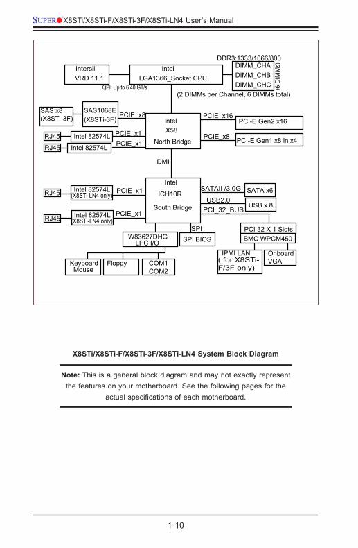
X8STi/X8STi-F/X8STi-3F/X8STi-LN4 System Block Diagram
Note: This is a general block diagram and may not exactly represent the features on your motherboard. See the following pages for the
actualspecificationsofeachmotherboard.
Intel
IntelVRD 11.1
Intel
Intersil
QPI: Up to 6.40 GT/s
PCIE_x16PCI-E Gen2 x16
X58
W83627DHG
COM1COM2
FloppyKeyboardMouse
SPISPI BIOS
ICH10R
LPC I/O
DMI
Intel 82574L PCIE_x1 RJ45
SATAII /3.0G
USB x 8
SATA x6USB2.0
DDR3:1333/1066/800
LGA1366_Socket CPU DIMM_CHBDIMM_CHA
DIMM_CHC
PCI 32 X 1 Slots
PCI_32_BUS
SAS1068EPCIE_x8SAS x8
(X8STi-3F)
BMC WPCM450
IPMI LAN Onboard VGA
PCI-E Gen1 x8 in x4PCIE_x8
(X8STi-3F)
PCIE_x1
( for X8STi-F/3F only)
(2 DIMMs per Channel, 6 DIMMs total)
Intel 82574L
(X8STi-LN4 only)
(6 D
IMM
s)
North Bridge
South Bridge
RJ45
PCIE_x1
Intel 82574LRJ45
(X8STi-LN4 only) Intel 82574LRJ45
PCIE_x1
Chapter 1: Introduction
1-11
1-2 Chipset Overview
Built upon the functionality and the capability of the Intel X58 Express chipset, the X8STi/X8STi-F/X8STi-3F/X8STi-LN4 motherboard provides the performance and featuresetrequiredforsingle-processor-basedhigh-endsystemswithconfigura-tion options optimized for intensive application and high-end server platforms.
The X8STi/X8STi-F/X8STi-3F/X8STi-LN4 supports the Intel® Core™ i7/Intel® Xeon® 5500/3500 series processors, the Intel X58 Express chipset, and the ICH10R. With Intel QuickPath Interconnect (QPI) technology built in, the X8STi/X8STi-F/X8STi-3F/X8STi-LN4isoneofthefirstmotherboardsonthemarketthatoffers the next generation point-to-point system interconnect interface, replacing the current Front Side Bus technology, providing substantial system performance enhancement by utilizing serial link interconnections to increase bandwidth and scalability.
Features of the LGA 1366 Processor and the X58 Chipset•Intel QuickPath Interconnect link, up to 6.4 GT/s of data transfer rate in each
direction
•Virtualization Technology, Integrated Management Engine support
•Point-to-point cache coherent interconnect, Fast/narrow unidirectional links, and Concurrentbi-directionaltraffic
•Error detection via CRC and Error correction via Link level retry
1-12
X8STi/X8STi-F/X8STi-3F/X8STi-LN4 User’s Manual
1-3 PC Health Monitoring
This section describes the PC health monitoring features of the X8STi/X8STi-F/X8STi-3F/X8STi-LN4. These features are supported by an onboard System Hard-ware Monitor chip.
Recovery from AC Power LossBIOS provides a setting for you to determine how the system will respond when AC power is lost and then restored to the system. You can choose for the system to remain powered off (in which case you must hit the power switch to turn it back on) or for it to automatically return to a power on state. See the Power Lost Control setting in the BIOS chapter of this manual to change this setting. The default set-ting is Last State.
Onboard Voltage Monitoring The onboard voltage monitor will scan the following voltages continuously: CPU Core, Chipset Voltage, Memory Voltage, +1.8V, +3.3V, +3.3V standby, +5V, +5V Standby, Vbat and ±12V. Once a voltage becomes unstable, it will give a warning or send an error message to the screen. Users can adjust the voltage thresholds todefinethesensitivityofthevoltagemonitorbyusingSDIII.
Fan Status Monitor with SoftwarePC health monitoring can check the RPM status of the cooling fans via Supero Doctor III.
CPU Overheat LED and Control This feature is available when the user enables the CPU overheat warning feature intheBIOS.Thisallowstheusertodefineanoverheattemperature.Whenthistem-peraturereachesthispre-definedoverheatthreshold,theCPUthermaltripfeaturewill be activated and it will send a signal to the buzzer and, at the same time, the CPU speed will be decreased.
1-4 PowerConfigurationSettings
This section describes the features of your motherboard that deal with power and power settings.
Chapter 1: Introduction
1-13
Slow Blinking LED for Suspend-State IndicatorWhen the CPU goes into a suspend state, the chassis power LED will start blink-ing to indicate that the CPU is in the suspend mode. When the user presses any key, the CPU will wake-up and the LED indicator will automatically stop blinking and remain on.
BIOS Support for USB KeyboardIf the USB keyboard is the only keyboard in the system, it will function like a normal keyboard during system boot-up.
Main Switch Override MechanismWhen an ATX power supply is used, the power button can function as a system suspend button. When the user presses the power button, the system will enter a SoftOff state. The monitor will be suspended and the hard drive will spin down. Pressing the power button again to wake-up the whole system. During the SoftOff state, the ATX power supply provides power the system to keep the required cir-cuitry "alive". In case the system malfunctions and you want to turn off the power, just press and hold the power button for 4 seconds. The power will turn off and no power will be provided to the motherboard.
Wake-On-LAN (WOL)Wake-On-LAN is definedas theability of amanagement application to remotelypower up a computer that is powered off. Remote PC setup, up-dates and asset trackingcanoccurafterhoursandonweekendssothatdailyLANtrafficiskepttoa minimum and users are not interrupted. The motherboard has a 3-pin header (WOL) to connect to the 3-pin header on a Network Interface Card (NIC) that has WOL capability. In addition, an onboard LAN controller can also support WOL without any connection to the WOL header. The 3-pin WOL header is to be used with a LAN add-on card only.
Note: Wake-On-LAN requires an ATX 2.01 (or above) compliant power supply.
1-5 Power Supply
As with all computer products, a stable power source is necessary for proper and reliable operation. It is even more important for processors that have high CPU clock rates of 1 GHz and faster.
The X8STi/X8STi-F/X8STi-3F/X8STi-LN4 accommodates ATX12V stan-dardpowersupplies.Althoughmostpowersuppliesgenerallymeetthespecifica-
1-14
X8STi/X8STi-F/X8STi-3F/X8STi-LN4 User’s Manual
tions required by the CPU, some are inadequate. A 2-Amp of current supply on a 5V Standby rail is strongly recommended.
It is strongly recommended that you use a high quality power supply that meets ATX12VstandardpowersupplySpecification1.1orabove.Itisalsorequiredthatthe 12V 8-pin power connection (JPW2) be used for adequate power supply. In areas where noisy power transmission is present, you may choose to install a line filter toshield thecomputer fromnoise. It isrecommendedthatyoualso installapower surge protector to help avoid problems caused by power surges.
1-6 Super I/O
Thediskdriveadapter functionsof theSuper I/Ochip includeafloppydiskdrivecontroller that is compatible with industry standard 82077/765, a data separator, write pre-compensation circuitry, decode logic, data rate selection, a clock genera-tor, drive interface control logic and interrupt and DMA logic. The wide range of functions integrated onto the Super I/O greatly reduces the number of components requiredforinterfacingwithfloppydiskdrives.TheSuperI/Osupportstwo360K,720 K, 1.2 M, 1.44 M or 2.88 M disk drives and data transfer rates of 250 Kb/s, 500 Kb/s or 1 Mb/s.
It also provides two high-speed, 16550 compatible serial communication ports (UARTs). Each UART includes a 16-byte send/receive FIFO, a programmable baud rate generator, complete modem control capability and a processor interrupt sys-tem. Both UARTs provide legacy speed with baud rate of up to 115.2 Kbps as well as an advanced speed with baud rates of 250 K, 500 K, or 1 Mb/s, which support higher speed modems.
TheSuperI/OprovidesfunctionsthatcomplywithACPI(AdvancedConfigurationand Power Interface), which includes support of legacy and ACPI power manage-ment through a SMI or SCI function pin. It also features auto power management to reduce power consumption.
1-7 Overview of the Winbond WPCM450 Controller (For X8STi-F/ X8STi-3F Only)
The Winbond WPCM450, a Baseboard Management Controller (BMC), supports the 2D/VGA-compatible Graphics Core with the PCI interface, Virtual Media, and Keyboard/Video/Mouse (KVM) Redirection modules.
The WPCM450 BMC interfaces with the host system via a PCI interface to com-municate with the graphics core. It supports USB 2.0 and 1.1 for remote keyboard/mouse/virtual media emulation. It also provides LPC interface to control Super IO functions. The WPCM450 is connected to the network via an external Ethernet PHY module.

Chapter 1: Introduction
1-15
The WPCM450 communicates with onboard components via six SMBus interfaces, fan control, Platform Environment Control Interface (PECI) buses, and General Purpose I/O (3SGPIO) ports.
The WPCM450 also includes the following features:
•One X-Bus parallel interface for expansion I/O connections
•Three ADC inputs, Analog and Digital Video outputs
•Two serial for boundary scan and debug
Note: For more information on IPMI configuration, please refer to the Embedded IPMI User's Guide posted on our website @ http://www.super-micro.com/support/manuals/.

1-16
X8STi/X8STi-F/X8STi-3F/X8STi-LN4 User’s Manual
Notes

Chapter 2: Installation
2-1
Chapter 2
Installation
2-1 Static-Sensitive Devices
Electrostatic-Discharge (ESD) can damage electronic com ponents. To prevent dam-age to your system board, it is important to handle it very carefully. The following measuresaregenerallysufficienttoprotectyourequipmentfromESD.
Precautions• Useagroundedwriststrapdesignedtopreventstaticdischarge.
• Touchagroundedmetal object before removing theboard from theantistaticbag.
• Handle the board by its edges only; do not touch its components, peripheralchips, memory modules or gold contacts.
• Whenhandlingchipsormodules,avoidtouchingtheirpins.
• Putthemotherboardandperipheralsbackintotheirantistaticbagswhennotinuse.
• Forgroundingpurposes,makesureyourcomputerchassisprovidesexcellentconductivity between the power supply, the case, the mounting fasteners and the motherboard.
• UseonlythecorrecttypeofonboardCMOSbattery.Donotinstalltheonboardupside down battery to avoid possible explosion.
UnpackingThe motherboard is shipped in antistatic packaging to avoid static damage. When unpacking the board, make sure the person handling it is static protected.
2-2
X8STi/X8STi-F/X8STi-3F/X8STi-LN4 User's Manual
2-2 Processor and Heatsink Installation
When handling the processor package, avoid placing direct pressure on the label area of the fan.
Notes: 1. Always connect the power cord last and always remove it before adding, re-
moving or changing any hardware components. Make sure that you install the processor into the CPU socket before you install the CPU heatsink.
2. Intel's boxed processor package contains the CPU fan and heatsink assem-bly.IfyoubuyaCPUseparately,makesurethatyouuseonlyIntel-certifiedmulti-directional heatsink and fan.
3. Make sure to install the motherboard into the chassis before you install the CPU heatsink and heatsink fans.
4. When purchasing an LGA 1366 processor or when receiving a motherboard with an LGA 1366 processor pre-installed, make sure that the CPU plastic capisinplace,andnoneoftheCPUpinsarebent;otherwise,contacttheretailer immediately.
5. Refer to the MB Features Section for more details on CPU support.
1. Press the socket clip to release the load plate, which covers the CPU socket, from its locking position.
2. Gently lift the socket clip to open the load plate.
3. Hold the plastic cap at its north and south center edges to re-move it from the CPU socket.
Note: The photos on this page and succeeding pag-es 2-3 through 2-9 are for illustration purposes only. They do not necessarily reflecttheexactproduct(s)described in this manual.
Socket Clip
!
Load Plate
Plastic Cap
Hold the north & south edges of the plastic cap to remove it
Installing an LGA 1366 Processor
Chapter 2: Installation
2-3
4. After removing the plastic cap, using yourthumbandtheindexfinger,hold the CPU at the north and south center edges.
5. Align the CPU key, the semi-circle cutout, against the socket key, the notch below the gold color dot on the side of the socket.
6. Once both the CPU and the socket are aligned, carefully lower the CPU straight down into the socket. (Do not rub the CPU against the surface of the socket or its pins to avoid damaging the CPU or the socket.)
7. With the CPU inside the socket, in-spect the four corners of the CPU to make sure that the CPU is properly installed.
8. Once the CPU is securely seated on the socket, lower the CPU load plate to the socket.
9. Use your thumb to gently push the socket clip down to the clip lock.
Warning: Please save the plas-tic cap. The motherboard must be shipped with the plastic cap properly installed to protect the CPU socket pins. Shipment without the plastic cap properly installed will cause damage to the socket pins.
CPU
CPU Socket
Load Plate
CPU
Align CPU keys with socket keys.
2-4
X8STi/X8STi-F/X8STi-3F/X8STi-LN4 User's Manual
Install a Heatsink Bracket on the reverse side of the board
Notes:
•A heatsink bracket (BKT_0023L) is required for a screw_type heatsink (-which is a non-pushpin heatskink as shown on the right.) The required heatsink bracket (BKT_0023L) can be purchased from Supermicro.
•Do not apply any thermal grease to the heatsink or the CPU die because the required amount has already been applied.
1. If you use a screw_type heatsink, please install a heatsink bracket (BKT_0023L) on the reverse side of the motherboard before installing the heatsink. (To install the heatsink bracket, please insert four screws to the mounting holes to secure the bracket on the motherboard.) If you do not use a screw_type heatsink, please skip this step.
2. Place the heatsink on top of the CPU so that the four mounting holes are aligned with those on the retention mechanism.
3. Install two diagonal screws (ie the #1 and the #2 screws) and tighten them until just snug (-do not fully tighten the screws to avoid possible damage to the CPU.)
4. Finish the installation by fully tight-ening all four screws.
Installing a Passive CPU Heatsink (#SNK-P0037)
Screw#1 Screw#2
Screw#1 Screw#2
Install Screw#1
Install Screw#2
Screw#1
Screw#3
Screw#4
Heatsink Bracket (BKT_0023L)
(for a Screw-Type Heatsink only)
Chapter 2: Installation
2-5
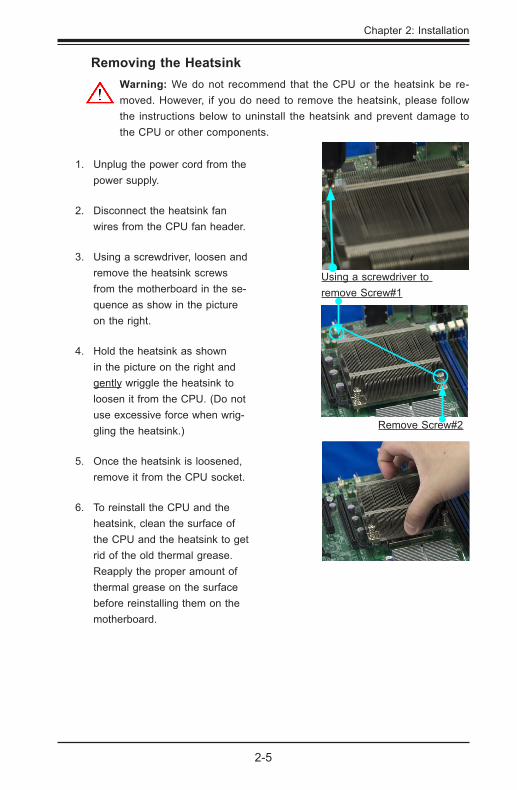
Removing the HeatsinkWarning: We do not recommend that the CPU or the heatsink be re-moved. However, if you do need to remove the heatsink, please follow the instructions below to uninstall the heatsink and prevent damage to the CPU or other components.
1. Unplug the power cord from the power supply.
2. Disconnect the heatsink fan wires from the CPU fan header.
3. Using a screwdriver, loosen and remove the heatsink screws from the motherboard in the se-quence as show in the picture on the right.
4. Hold the heatsink as shown in the picture on the right and gently wriggle the heatsink to loosen it from the CPU. (Do not use excessive force when wrig-gling the heatsink.)
5. Once the heatsink is loosened, remove it from the CPU socket.
6. To reinstall the CPU and the heatsink, clean the surface of the CPU and the heatsink to get rid of the old thermal grease. Reapply the proper amount of thermal grease on the surface before reinstalling them on the motherboard.
Using a screwdriver to remove Screw#1
Remove Screw#2
2-6
X8STi/X8STi-F/X8STi-3F/X8STi-LN4 User's Manual
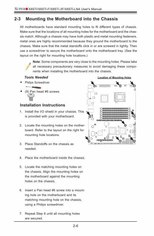
2-3 Mounting the Motherboard into the Chassis
Allmotherboards have standardmounting holes to fit different types of chassis.Make sure that the locations of all mounting holes for the motherboard and the chas-sis match. Although a chassis may have both plastic and metal mounting fasteners, metal ones are highly recommended because they ground the motherboard to the chassis. Make sure that the metal standoffs click in or are screwed in tightly. Then use a screwdriver to secure the motherboard onto the motherboard tray. (See the layout on the right for mounting hole locations.)
Note: Some components are very close to the mounting holes. Please take all necessary precautionary measures to avoid damaging these compo-nents when installing the motherboard into the chassis.
Tools Needed•Philips Screwdriver
•(9) Pan head #6 screws
Installation Instructions1. Install the I/O shield in your chassis. This
is provided with your motherboard.
2. Locate the mounting holes on the mother-board. Refer to the layout on the right for mounting hole locations.
3. Place Standoffs on the chassis as needed.
4. Place the motherboard inside the chassis.
5. Locate the matching mounting holes on the chassis. Align the mounting holes on the motherboard against the mounting holes on the chassis.
6. Insert a Pan head #6 screw into a mount-ing hole on the motherboard and its matching mounting hole on the chassis, using a Philips screwdriver.
7. Repeat Step 6 until all mounting holes are secured.
Pan head6-32 x 5 mm
[0.197]
Location of Mounting Holes
Chapter 2: Installation
2-7
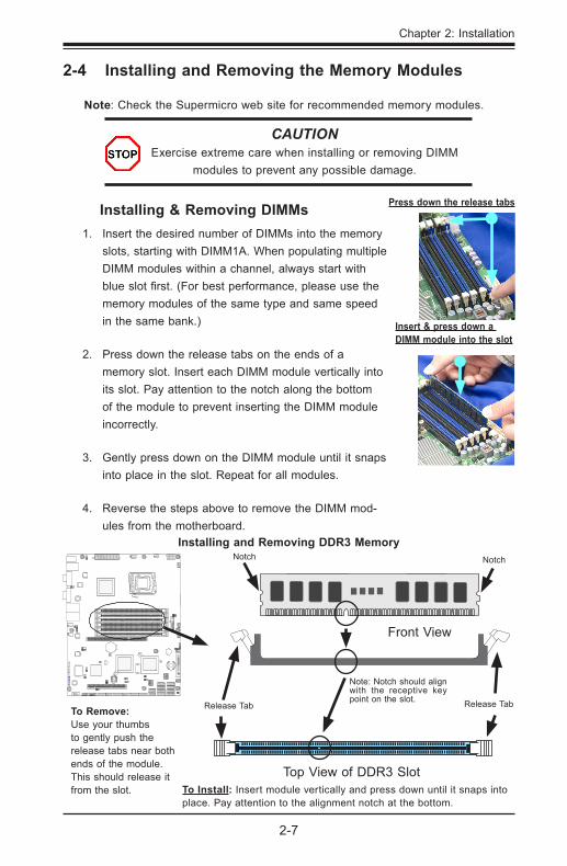
2-4 Installing and Removing the Memory Modules
Note: Check the Supermicro web site for recommended memory modules.
CAUTION Exercise extreme care when installing or removing DIMM
modules to prevent any possible damage.
To Install: Insert module vertically and press down until it snaps into place. Pay attention to the alignment notch at the bottom.
To Remove: Use your thumbs to gently push the release tabs near both ends of the module. This should release it from the slot.
Press down the release tabs
Insert & press down a DIMM module into the slot
Installing & Removing DIMMs1. Insert the desired number of DIMMs into the memory
slots, starting with DIMM1A. When populating multiple DIMM modules within a channel, always start with blueslotfirst.(Forbestperformance,pleaseusethememory modules of the same type and same speed in the same bank.)
2. Press down the release tabs on the ends of a memory slot. Insert each DIMM module vertically into its slot. Pay attention to the notch along the bottom of the module to prevent inserting the DIMM module incorrectly.
3. Gently press down on the DIMM module until it snaps into place in the slot. Repeat for all modules.
4. Reverse the steps above to remove the DIMM mod-ules from the motherboard.
Installing and Removing DDR3 Memory
Top View of DDR3 Slot
Release Tab Release Tab
Note: Notch should align with the receptive key point on the slot.
Notch Notch
Front View
2-8
X8STi/X8STi-F/X8STi-3F/X8STi-LN4 User's Manual
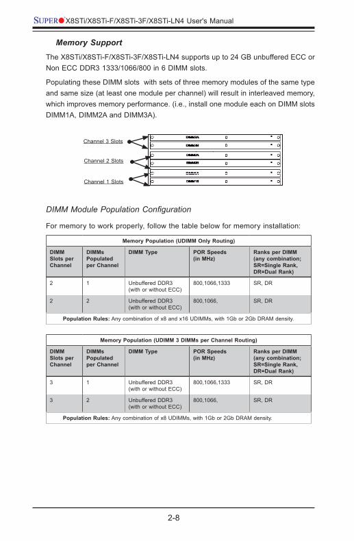
Memory Support
The X8STi/X8STi-F/X8STi-3F/X8STi-LN4 supports up to 24 GB unbuffered ECC or Non ECC DDR3 1333/1066/800 in 6 DIMM slots.
Populating these DIMM slots with sets of three memory modules of the same type and same size (at least one module per channel) will result in interleaved memory, which improves memory performance. (i.e., install one module each on DIMM slots DIMM1A, DIMM2A and DIMM3A).
Channel 1 Slots
Channel 2 Slots
Channel 3 Slots
DIMM Module Population Configuration
For memory to work properly, follow the table below for memory installation:
Memory Population (UDIMM Only Routing)
DIMM Slots per Channel
DIMMs Populated per Channel
DIMM Type POR Speeds (in MHz)
Ranks per DIMM (any combination; SR=Single Rank,DR=Dual Rank)
2 1 Unbuffered DDR3 (with or without ECC)
800,1066,1333 SR, DR
2 2 Unbuffered DDR3(with or without ECC)
800,1066, SR, DR
Population Rules: Any combination of x8 and x16 UDIMMs, with 1Gb or 2Gb DRAM density.
Memory Population (UDIMM 3 DIMMs per Channel Routing)
DIMM Slots per Channel
DIMMs Populated per Channel
DIMM Type POR Speeds (in MHz)
Ranks per DIMM (any combination; SR=Single Rank,DR=Dual Rank)
3 1 Unbuffered DDR3 (with or without ECC)
800,1066,1333 SR, DR
3 2 Unbuffered DDR3(with or without ECC)
800,1066, SR, DR
Population Rules: Any combination of x8 UDIMMs, with 1Gb or 2Gb DRAM density.
Chapter 2: Installation
2-9
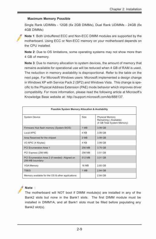
Possible System Memory Allocation & Availability
System Device Size Physical Memory Remaining (-Available)(4 GB Total System Memory)
FirmwareHubflashmemory(SystemBIOS) 1 MB 3.99 GB
Local APIC 4 KB 3.99 GB
Area Reserved for the chipset 2 MB 3.99 GB
I/O APIC (4 Kbytes) 4 KB 3.99 GB
PCI Enumeration Area 1 256 MB 3.76 GB
PCI Express (256 MB) 256 MB 3.51 GB
PCI Enumeration Area 2 (if needed) -Aligned on 256-MB boundary-
512 MB 3.01 GB
VGA Memory 16 MB 2.85 GB
TSEG 1 MB 2.84 GB
Memory available for the OS & other applications 2.84 GB
Note : The motherboard will NOT boot if DIMM module(s) are installed in any of the Bank2 slots but none in the Bank1 slots. The first DIMM module must beinstalled in DIMM1A, and all Bank1 slotsmust be filled before populating anyBank2 slot(s).
Maximum Memory Possible
Single Rank UDIMMs - 12GB (6x 2GB DIMMs), Dual Rank UDIMMs - 24GB (6x 4GB DIMMs)
Note 1: Both Unbuffered ECC and Non-ECC DIMM modules are supported by the motherboard. Using ECC or Non-ECC memory on your motherboard depends on the CPU installed.
Note 2: Due to OS limitations, some operating systems may not show more than 4 GB of memory.
Note 3: Due to memory allocation to system devices, the amount of memory that remains available for operational use will be reduced when 4 GB of RAM is used. The reduction in memory availability is disproportional. Refer to the table on the next page. For Microsoft Windows users: Microsoft implemented a design change in Windows XP with Service Pack 2 (SP2) and Windows Vista. This change is spe-cifictothePhysicalAddressExtension(PAE)modebehaviorwhichimprovesdrivercompatibility. For more information, please read the following article at Microsoft’s Knowledge Base website at: http://support.microsoft.com/kb/888137.
2-10
X8STi/X8STi-F/X8STi-3F/X8STi-LN4 User's Manual
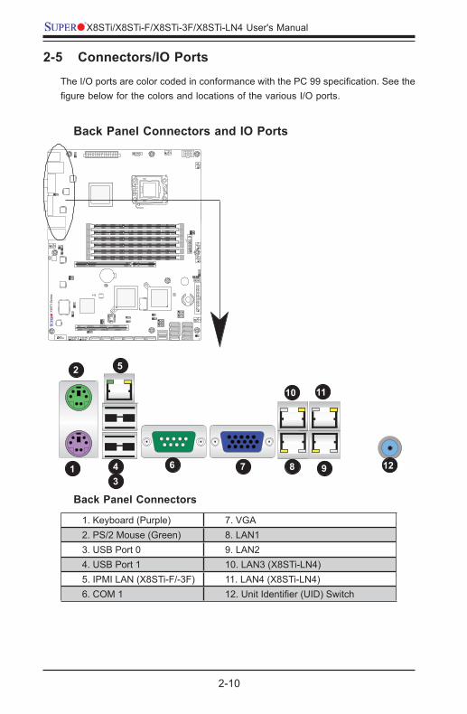
2-5 Connectors/IO Ports
TheI/OportsarecolorcodedinconformancewiththePC99specification.SeethefigurebelowforthecolorsandlocationsofthevariousI/Oports.
Back Panel Connectors and IO Ports
Back Panel Connectors
1. Keyboard (Purple) 7. VGA2. PS/2 Mouse (Green) 8. LAN13. USB Port 0 9. LAN24. USB Port 1 10. LAN3 (X8STi-LN4)5. IPMI LAN (X8STi-F/-3F) 11. LAN4 (X8STi-LN4)6. COM 1 12.UnitIdentifier(UID)Switch
1
2
34
5
6 7 8 9
10 11
12
Chapter 2: Installation
2-11
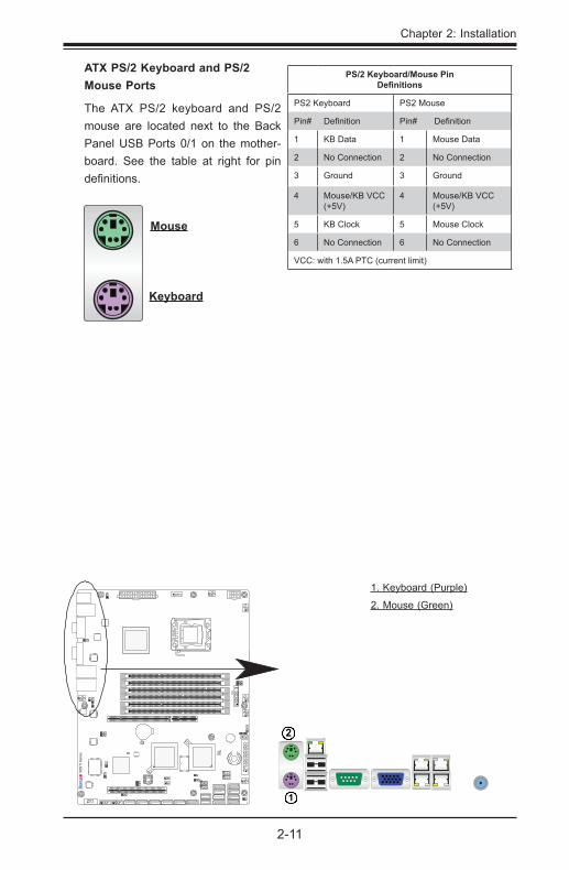
ATX PS/2 Keyboard and PS/2 Mouse Ports
The ATX PS/2 keyboard and PS/2 mouse are located next to the Back Panel USB Ports 0/1 on the mother-board. See the table at right for pin definitions.
PS/2 Keyboard/Mouse Pin Definitions
PS2 Keyboard PS2 Mouse
Pin#Definition Pin#Definition
1 KB Data 1 Mouse Data
2 No Connection 2 No Connection
3 Ground 3 Ground
4 Mouse/KB VCC (+5V)
4 Mouse/KB VCC (+5V)
5 KB Clock 5 Mouse Clock
6 No Connection 6 No Connection
VCC: with 1.5A PTC (current limit)
1
2
1. Keyboard (Purple)
2. Mouse (Green)
Keyboard
Mouse
2-12
X8STi/X8STi-F/X8STi-3F/X8STi-LN4 User's Manual
LSI 1068E
NIC
4 LE
D
JBM
C1
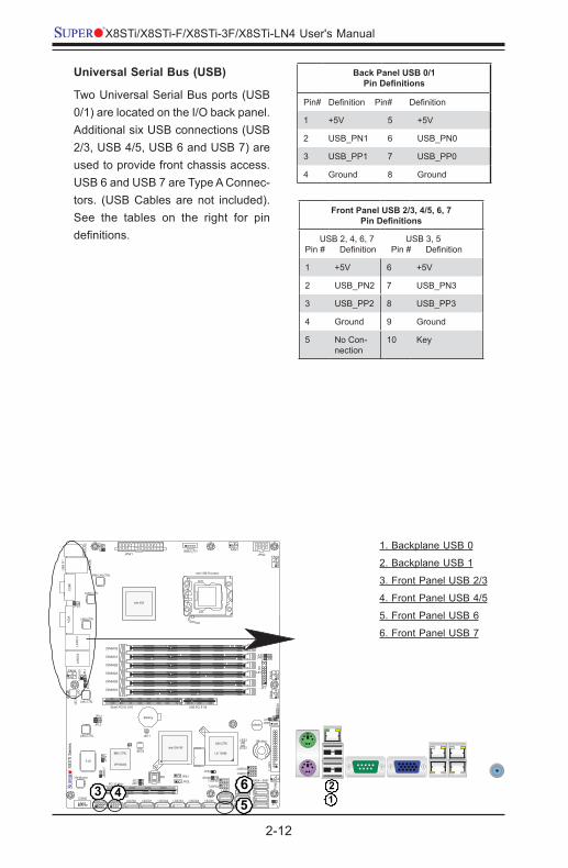
1. Backplane USB 0
2. Backplane USB 1
3. Front Panel USB 2/3
4. Front Panel USB 4/5
5. Front Panel USB 6
6. Front Panel USB 7
Universal Serial Bus (USB)
Two Universal Serial Bus ports (USB 0/1) are located on the I/O back panel. Additional six USB connections (USB 2/3, USB 4/5, USB 6 and USB 7) are used to provide front chassis access. USB 6 and USB 7 are Type A Connec-tors. (USB Cables are not included). See the tables on the right for pin definitions.
Back Panel USB 0/1PinDefinitions
Pin#DefinitionPin#Definition
1 +5V 5 +5V
2 USB_PN1 6 USB_PN0
3 USB_PP1 7 USB_PP0
4 Ground 8 Ground
Front Panel USB 2/3, 4/5, 6, 7PinDefinitions
USB 2, 4, 6, 7 Pin#Definition
USB 3, 5Pin#Definition
1 +5V 6 +5V
2 USB_PN2 7 USB_PN3
3 USB_PP2 8 USB_PP3
4 Ground 9 Ground
5 No Con-nection
10 Key
4356
12
Chapter 2: Installation
2-13
Ethernet Ports
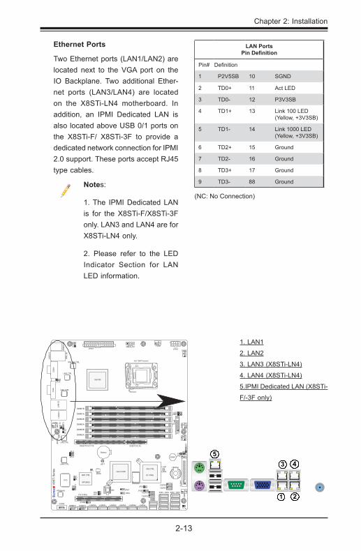
Two Ethernet ports (LAN1/LAN2) are located next to the VGA port on the IO Backplane. Two additional Ether-net ports (LAN3/LAN4) are located on the X8STi-LN4 motherboard. In addition, an IPMI Dedicated LAN is also located above USB 0/1 ports on the X8STi-F/ X8STi-3F to provide a dedicated network connection for IPMI 2.0 support. These ports accept RJ45 type cables.
Notes:
1. The IPMI Dedicated LAN is for the X8STi-F/X8STi-3F only. LAN3 and LAN4 are for X8STi-LN4 only.
2. Please refer to the LED Indicator Section for LAN LED information.
LAN PortsPinDefinition
Pin#Definition
1 P2V5SB 10 SGND
2 TD0+ 11 Act LED
3 TD0- 12 P3V3SB
4 TD1+ 13 Link 100 LED (Yellow, +3V3SB)
5 TD1- 14 Link 1000 LED (Yellow, +3V3SB)
6 TD2+ 15 Ground
7 TD2- 16 Ground
8 TD3+ 17 Ground
9 TD3- 88 Ground
(NC: No Connection)
1. LAN1
2. LAN2
3. LAN3 (X8STi-LN4)
4. LAN4 (X8STi-LN4)
5.IPMI Dedicated LAN (X8STi-
F/-3F only)
3
1 2
LSI 1068E
NIC
4 LE
D
JBM
C1
45
2-14
X8STi/X8STi-F/X8STi-3F/X8STi-LN4 User's Manual
1
2
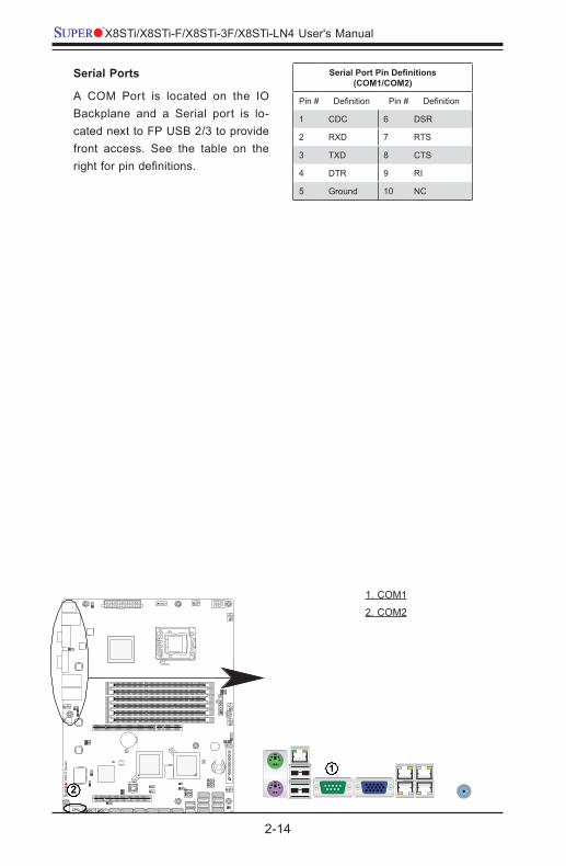
Serial Ports
A COM Port is located on the IO Backplane and a Serial port is lo-cated next to FP USB 2/3 to provide front access. See the table on the rightforpindefinitions.
SerialPortPinDefinitions(COM1/COM2)
Pin#Definition Pin#Definition
1 CDC 6 DSR
2 RXD 7 RTS
3 TXD 8 CTS
4 DTR 9 RI
5 Ground 10 NC
1. COM1
2. COM2
Chapter 2: Installation
2-15
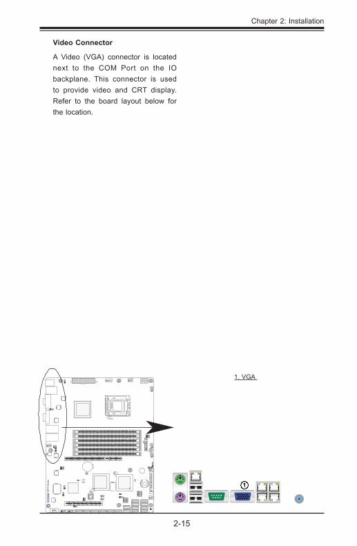
1. VGA
Video Connector
A Video (VGA) connector is located next to the COM Port on the IO backplane. This connector is used to provide video and CRT display. Refer to the board layout below for the location.
1
2-16
X8STi/X8STi-F/X8STi-3F/X8STi-LN4 User's Manual
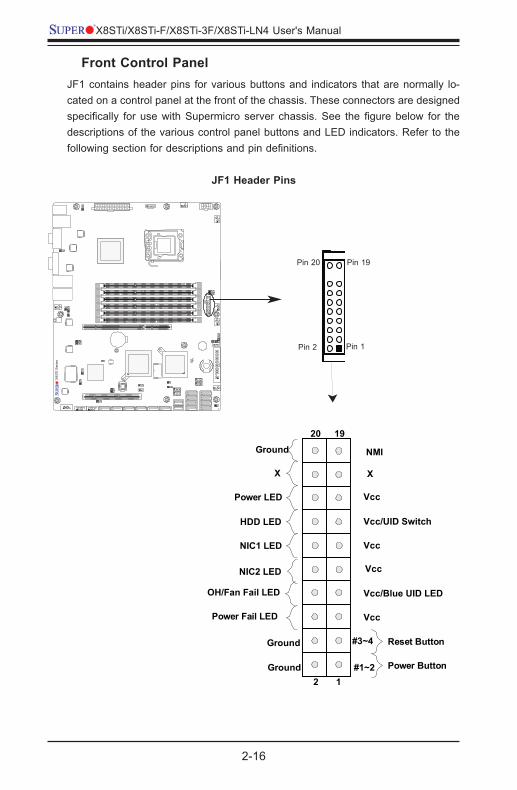
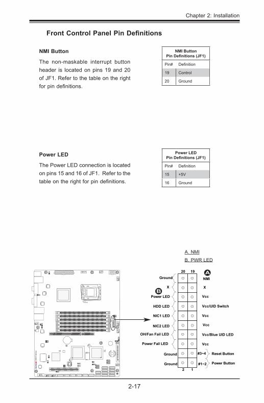
Front Control PanelJF1 contains header pins for various buttons and indicators that are normally lo-cated on a control panel at the front of the chassis. These connectors are designed specifically for usewithSupermicro server chassis.See the figurebelow for thedescriptions of the various control panel buttons and LED indicators. Refer to the followingsectionfordescriptionsandpindefinitions.
JF1 Header Pins
Pin 19Pin 20
Pin 1Pin 2
Power Button
OH/Fan Fail LED
1
NIC1 LED
Reset Button
2
Power Fail LED
HDD LED
Power LED
#3~4
#1~2
Vcc
Vcc/UID Switch
Vcc
Vcc/Blue UID LED
Ground
Ground
1920
Vcc
X
Ground NMI
X
VccNIC2 LED
Chapter 2: Installation
2-17
FrontControlPanelPinDefinitions
Power LED
The Power LED connection is located on pins 15 and 16 of JF1. Refer to the tableontherightforpindefinitions.
NMI Button
The non-maskable interrupt button header is located on pins 19 and 20 of JF1. Refer to the table on the right forpindefinitions.
Power Button
OH/Fan Fail LED
1
NIC1 LED
Reset Button
2
Power Fail LED
HDD LED
Power LED
#3~4
#1~2
Vcc
Vcc/UID Switch
Vcc
Vcc/Blue UID LED
Ground
Ground
1920
Vcc
X
Ground NMI
X
VccNIC2 LED
NMI Button PinDefinitions(JF1)
Pin#Definition
19 Control
20 Ground
Power LEDPinDefinitions(JF1)
Pin#Definition
15 +5V
16 Ground
A. NMI
B. PWR LED
A
B
2-18
X8STi/X8STi-F/X8STi-3F/X8STi-LN4 User's Manual
Power Button
OH/Fan Fail LED
1
NIC1 LED
Reset Button
2
Power Fail LED
HDD LED
Power LED
#3~4
#1~2
Vcc
Vcc/UID Switch
Vcc
Vcc/Blue UID LED
Ground
Ground
1920
Vcc
X
Ground NMI
X
VccNIC2 LED
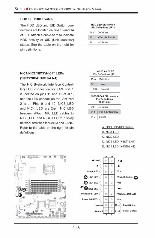
NIC1/NIC2/NIC3*/NIC4* LEDs (*NIC3/NIC4: X8STi-LN4)
The NIC (Network Interface Control-ler) LED connection for LAN port 1 is located on pins 11 and 12 of JF1, and the LED connection for LAN Port 2 is on Pins 9 and 10. NIC3_LED and NIC4_LED are 2-pin NIC LED headers. Attach NIC LED cables to NIC3_LED and NIC4_LED to display network activities for LAN 3 and LAN4. Refer to the table on the right for pin definitions.
HDD LED/UID Switch
The HDD LED and UID Switch con-nections are located on pins 13 and 14 of JF1. Attach a cable here to indicate HDD activity or UID (Unit Identifier)status. See the table on the right for pindefinitions.
HDD LED/UID SwitchPinDefinitions(JF1)
Pin#Definition
13 +5V/UID Switch
14 HD Active
LAN1/LAN2 LEDPinDefinitions(JF1)
Pin#Definition
9/11 Vcc
10/12 Ground
A
B
C
A. HDD LED/UID Switch
B. NIC1 LED
C. NIC2 LED
D. NIC3 LED (X8STi-LN4)
E. NIC4 LED (X8STi-LN4)
LSI 1068E
NIC
4 LE
D
JBM
C1
DB
NIC3/NIC4 LED HeadersPinDefinitions
(X8STi-LN4)
Pin#Definition
Pin 1 Vcc 3.3V Standby
Pin 2 Signal
E
A
Chapter 2: Installation
2-19
Power Button
OH/Fan Fail LED
1
NIC1 LED
Reset Button
2
Power Fail LED
HDD LED
Power LED
#3~4
#1~2
Vcc
Vcc/UID Switch
Vcc
Vcc/Blue UID LED
Ground
Ground
1920
Vcc
X
Ground NMI
X
VccNIC2 LED
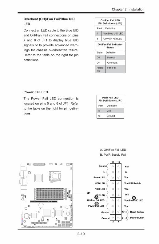
Overheat (OH)/Fan Fail/Blue UID LED
Connect an LED cable to the Blue UID and OH/Fan Fail connections on pins 7 and 8 of JF1 to display blue UID signals or to provide advanced warn-ings for chassis overheat/fan failure. Refer to the table on the right for pin definitions.
Power Fail LED
The Power Fail LED connection is located on pins 5 and 6 of JF1. Refer tothetableontherightforpindefini-tions.
OH/Fan Fail LEDPinDefinitions(JF1)
Pin#Definition
7 Vcc/Blue UID LED
8 OH/Fan Fail LED
OH/Fan Fail Indicator Status
StateDefinition
Off Normal
On Overheat
Flash-ing
Fan Fail
PWR Fail LEDPinDefinitions(JF1)
Pin#Definition
5 Vcc
6 Ground
A
B
A. OH/Fan Fail LED
B. PWR Supply Fail
A
2-20
X8STi/X8STi-F/X8STi-3F/X8STi-LN4 User's Manual
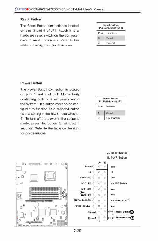
Power Button
The Power Button connection is located on pins 1 and 2 of JF1. Momentarily contacting both pins will power on/off the system. This button can also be con-figured to functionasa suspendbutton(with a setting in the BIOS - see Chapter 4). To turn off the power in the suspend mode, press the button for at least 4 seconds. Refer to the table on the right forpindefinitions.
Power ButtonPinDefinitions(JF1)
Pin#Definition
1 Signal
2 +3V Standby
Reset Button
The Reset Button connection is located on pins 3 and 4 of JF1. Attach it to a hardware reset switch on the computer case to reset the system. Refer to the tableontherightforpindefinitions.
Reset ButtonPinDefinitions(JF1)
Pin#Definition
3 Reset
4 Ground
A. Reset Button
B. PWR Button
A
BPower Button
OH/Fan Fail LED
1
NIC1 LED
Reset Button
2
Power Fail LED
HDD LED
Power LED
#3~4
#1~2
Vcc
Vcc/UID Switch
Vcc
Vcc/Blue UID LED
Ground
Ground
1920
Vcc
X
Ground NMI
X
VccNIC2 LED

Chapter 2: Installation
2-21
LSI 1068E
NIC
4 LE
D
JBM
C1
2-6 Connecting Cables
Thissectionprovidesbriefdescriptionsandpin-outdefinitionsforonboardheadersand connectors. Be sure to use the correct cable for each header or connector. • For informationonBackpanelUSBandFrontPanelUSBports, refer toPage2-14.
• For information on COM Port 1 and COM Port 2, please see Page 2-16.
A. 24-Pin ATX Main PWR
B. 8-Pin Processor PWR
A B
ATX Power 24-pin ConnectorPinDefinitions(JPW1)
Pin#DefinitionPin#Definition
13 +3.3V 1 +3.3V
14 -12V 2 +3.3V
15 COM 3 COM
16 PS_ON 4 +5V
17 COM 5 COM
18 COM 6 +5V
19 COM 7 COM
20 Res (NC) 8 PWR_OK
21 +5V 9 5VSB
22 +5V 10 +12V
23 +5V 11 +12V
24 COM 12 +3.3V
(Required)
12V 8-pin Power Connec-torPinDefinitions
PinsDefinition
1 through 4 Ground
5 through 8 +12V
ATX Main PWR & CPU PWR Connectors
The 24-pin main power connector (JPW1) is used to provide power to the motherboard. The 8-pin CPU PWR connector (JPW2) is also required for the processor. These power connec-torsmeettheSSIEPS12Vspecifica-tion. See the table on the right for pin definitions.
2-22
X8STi/X8STi-F/X8STi-3F/X8STi-LN4 User's Manual
LSI 1068E
NIC
4 LE
D
JBM
C1
Fan HeaderPinDefinitions
Pin#Definition
1 Ground (Black)
2 2.5A/+16V (Red)
3 Tachometer
4 PWM_Control
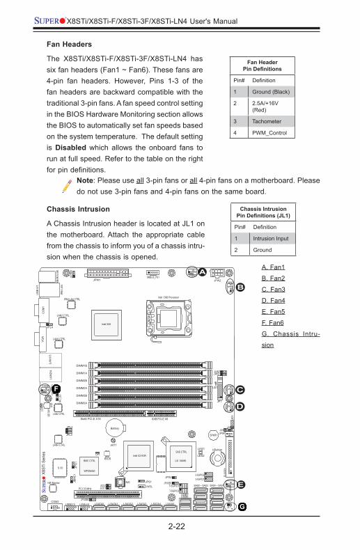
Fan Headers
The X8STi/X8STi-F/X8STi-3F/X8STi-LN4 has six fan headers (Fan1 ~ Fan6). These fans are 4-pin fan headers. However, Pins 1-3 of the fan headers are backward compatible with the traditional 3-pin fans. A fan speed control setting in the BIOS Hardware Monitoring section allows the BIOS to automatically set fan speeds based on the system temperature. The default setting is Disabled which allows the onboard fans to run at full speed. Refer to the table on the right forpindefinitions.
A
B
A. Fan1
B. Fan2
C. Fan3
D. Fan4
E. Fan5
F. Fan6
G. Chassis Intru-
sion
C
D
E
F
G
Chassis Intrusion
A Chassis Intrusion header is located at JL1 on the motherboard. Attach the appropriate cable from the chassis to inform you of a chassis intru-sion when the chassis is opened.
Chassis IntrusionPinDefinitions(JL1)
Pin#Definition
1 Intrusion Input
2 Ground
Note: Please use all 3-pin fans or all 4-pin fans on a motherboard. Please do not use 3-pin fans and 4-pin fans on the same board.
Chapter 2: Installation
2-23
LSI 1068E
NIC
4 LE
D
JBM
C1
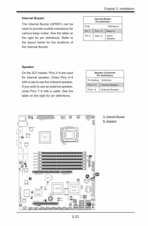
Internal Buzzer
The Internal Buzzer (SPKR1) can be used to provide audible indications for various beep codes. See the table on the right for pin definitions. Refer tothe layout below for the locations of the Internal Buzzer.
A. Internal Buzzer
B. Speaker
Internal BuzzerPinDefinition
Pin#Definitions
Pin 1 Pos. (+) Beep In
Pin 2 Neg. (-) Alarm Speaker
Speaker
On the JD1 header, Pins 3~4 are used for internal speaker. Close Pins 3~4 with a cap to use the onboard speaker. If you wish to use an external speaker, close Pins 1~4 with a cable. See the tableontherightforpindefinitions.
Speaker ConnectorPinDefinitions
PinSettingDefinition
Pins 3~4 Internal Speaker
Pins1~4 External Speaker
A B
C
2-24
X8STi/X8STi-F/X8STi-3F/X8STi-LN4 User's Manual
LSI 1068E
NIC
4 LE
D
JBM
C1
A. Overheat/Fan Fail LED
B. NIC3_LED (X8STi-LN4)
C. NIC4_LED (X8STi-LN4)
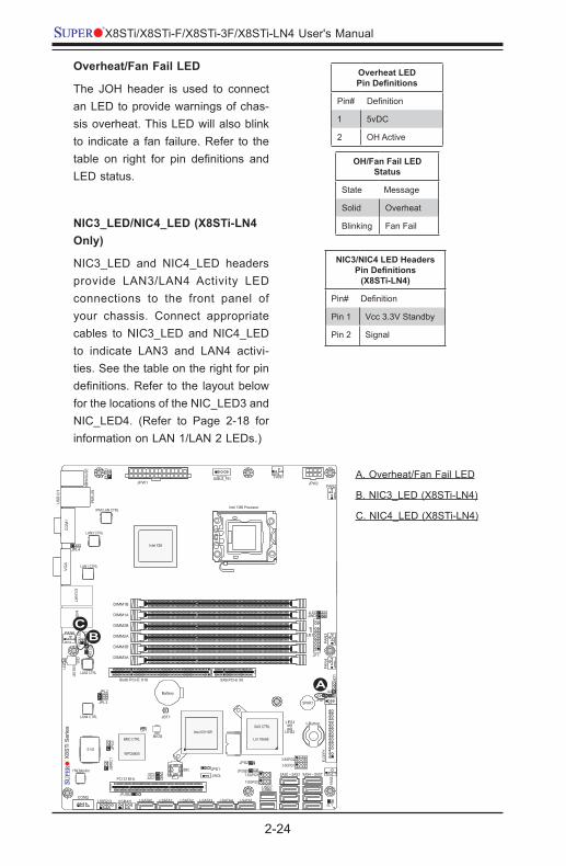
Overheat/Fan Fail LED
The JOH header is used to connect an LED to provide warnings of chas-sis overheat. This LED will also blink to indicate a fan failure. Refer to the table on right for pin definitions andLED status.
Overheat LEDPinDefinitions
Pin#Definition
1 5vDC
2 OH Active
OH/Fan Fail LEDStatus
State Message
Solid Overheat
Blinking Fan Fail
A
B
NIC3_LED/NIC4_LED (X8STi-LN4 Only)
NIC3_LED and NIC4_LED headers provide LAN3/LAN4 Activity LED connections to the front panel of your chassis. Connect appropriate cables to NIC3_LED and NIC4_LED to indicate LAN3 and LAN4 activi-ties. See the table on the right for pin definitions.Refer to the layoutbelowfor the locations of the NIC_LED3 and NIC_LED4. (Refer to Page 2-18 for information on LAN 1/LAN 2 LEDs.)
C
NIC3/NIC4 LED HeadersPinDefinitions
(X8STi-LN4)
Pin#Definition
Pin 1 Vcc 3.3V Standby
Pin 2 Signal
Chapter 2: Installation
2-25
LSI 1068E
NIC
4 LE
D
JBM
C1
A. PWR LED
B. PWR SMB
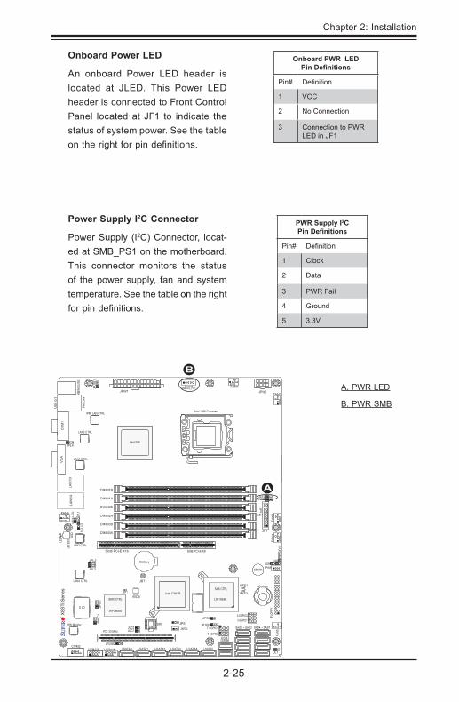
Power Supply I2C Connector
Power Supply (I2C) Connector, locat-ed at SMB_PS1 on the motherboard. This connector monitors the status of the power supply, fan and system temperature. See the table on the right forpindefinitions.
PWR Supply I2CPinDefinitions
Pin#Definition
1 Clock
2 Data
3 PWR Fail
4 Ground
5 3.3V
Onboard Power LED
An onboard Power LED header is located at JLED. This Power LED header is connected to Front Control Panel located at JF1 to indicate the status of system power. See the table ontherightforpindefinitions.
Onboard PWR LEDPinDefinitions
Pin#Definition
1 VCC
2 No Connection
3 Connection to PWR LED in JF1
A
B
2-26
X8STi/X8STi-F/X8STi-3F/X8STi-LN4 User's Manual
LSI 1068E
NIC
4 LE
D
JBM
C1
Serial_Link-SGPIOPinDefinitions
Pin#Definition PinDefinition
1 NC 2 NC
3 Ground 4 DATA Out
5 Load 6 Ground
7 Clock 8 NC
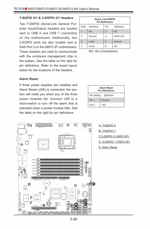
T-SGPIO 0/1 & 3-SGPIO 0/1 Headers
Two T-SGPIO (Serial-Link General Pur-pose Input/Output) headers are located next to USB 6 and USB 7 connectors on the motherboard. Additionally, two 3-SGPIO ports are also located next to SAS Port 3 on the X8STi-3F motherboard. These headers are used to communicate with the enclosure management chip in the system. See the table on the right for pin definitions.Refer to the board layoutbelow for the locations of the headers.
NC: No Connections
A. T-SGPIO 0
B. T-SGPIO 1
C.3-SGPIO 0 (X8STi-3F)
D. 3-SGPIO 1 (X8STi-3F)
E. Alarm Reset
CD
AB
Alarm Reset
If three power supplies are installed and Alarm Reset (JAR) is connected, the sys-tem will notify you when any of the three power modules fail. Connect JAR to a micro-switch to turn off the alarm that is activated when a power module fails. See thetableontherightforpindefinitions.
Alarm Reset PinDefinitions
PinSettingDefinition
Pin 1 Ground
Pin 2 +5V
E
Chapter 2: Installation
2-27
LSI 1068E
NIC
4 LE
D
JBM
C1
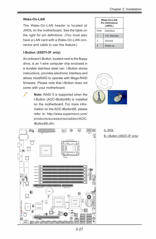
Wake-On-LAN
The Wake-On-LAN header is located at JWOL on the motherboard. See the table on the right forpindefinitions. (Youmustalsohave a LAN card with a Wake-On-LAN con-nector and cable to use this feature.)
Wake-On-LANPinDefinitions
(JWOL)
Pin#Definition
1 +5V Standby
2 Ground
3 Wake-up
A. WOL
B. I-Button (X8STi-3F only)
A
B
I-Button (X8STi-3F only)
AnonboardI-Button,locatednexttothefloppydrive, is an 1-wire computer chip enclosed in a durable stainless steel can. I-Button stores instructions, provides electronic interface and allows HostRAID to operate with Mega-RAID firmware.PleasenotethatI-Buttondoesnotcome with your motherboard.
Note: RAID 5 is supported when the I-Button (AOC-IButton68) is installed on the motherboard. For more infor-mation on the AOC-IButton68, please refer to http://www.supermicro.com/products/accessories/addon/AOC-IButton68.cfm.
2-28
X8STi/X8STi-F/X8STi-3F/X8STi-LN4 User's Manual
LSI 1068E
NIC
4 LE
D
JBM
C1
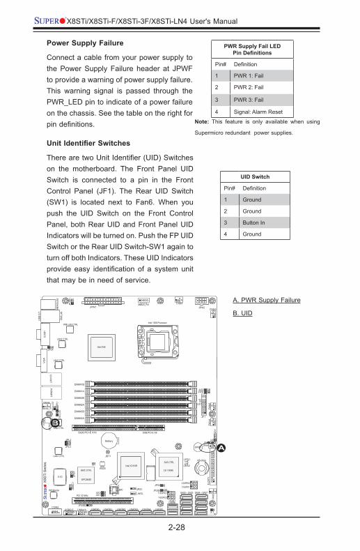
A. PWR Supply Failure
B. UID
A
B
Power Supply Failure
Connect a cable from your power supply to the Power Supply Failure header at JPWF to provide a warning of power supply failure. This warning signal is passed through the PWR_LED pin to indicate of a power failure on the chassis. See the table on the right for pindefinitions. Note: This feature is only available when using
Supermicro redundant power supplies.
PWR Supply Fail LEDPinDefinitions
Pin#Definition
1 PWR 1: Fail
2 PWR 2: Fail
3 PWR 3: Fail
4 Signal: Alarm Reset
UnitIdentifierSwitches
TherearetwoUnitIdentifier(UID)Switcheson the motherboard. The Front Panel UID Switch is connected to a pin in the Front Control Panel (JF1). The Rear UID Switch (SW1) is located next to Fan6. When you push the UID Switch on the Front Control Panel, both Rear UID and Front Panel UID Indicators will be turned on. Push the FP UID Switch or the Rear UID Switch-SW1 again to turn off both Indicators. These UID Indicators provide easy identification of a systemunitthat may be in need of service.
UID Switch
Pin#Definition
1 Ground
2 Ground
3 Button In
4 Ground
Chapter 2: Installation
2-29
LSI 1068E
NIC
4 LE
D
JBM
C1
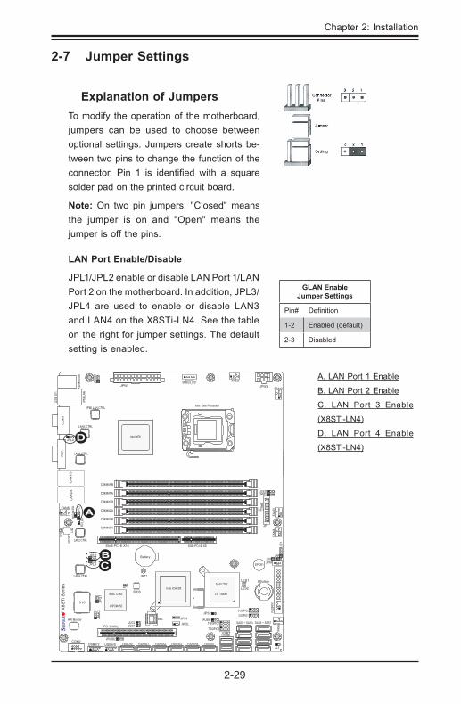
2-7 Jumper Settings
Explanation of JumpersTo modify the operation of the motherboard, jumpers can be used to choose between optional settings. Jumpers create shorts be-tween two pins to change the function of the connector. Pin 1 is identified with a squaresolder pad on the printed circuit board.
Note: On two pin jumpers, "Closed" means the jumper is on and "Open" means the jumper is off the pins.
A
A. LAN Port 1 Enable
B. LAN Port 2 Enable
C. LAN Port 3 Enable
(X8STi-LN4)
D. LAN Port 4 Enable
(X8STi-LN4)
LAN Port Enable/Disable
JPL1/JPL2 enable or disable LAN Port 1/LAN Port 2 on the motherboard. In addition, JPL3/JPL4 are used to enable or disable LAN3 and LAN4 on the X8STi-LN4. See the table on the right for jumper settings. The default setting is enabled.
GLAN EnableJumper Settings
Pin#Definition
1-2 Enabled (default)
2-3 Disabled
BC
D
2-30
X8STi/X8STi-F/X8STi-3F/X8STi-LN4 User's Manual
LSI 1068E
NIC
4 LE
D
JBM
C1
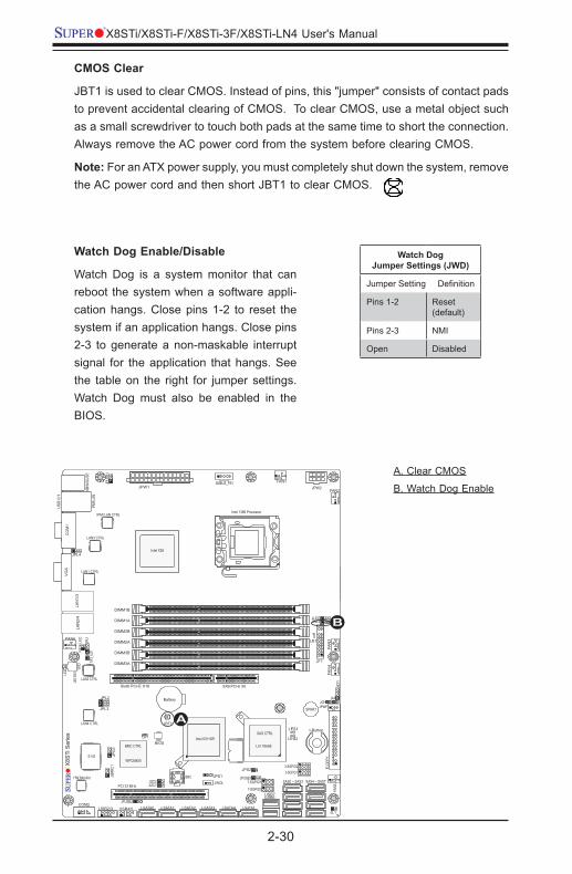
CMOS Clear
JBT1 is used to clear CMOS. Instead of pins, this "jumper" consists of contact pads to prevent accidental clearing of CMOS. To clear CMOS, use a metal object such as a small screwdriver to touch both pads at the same time to short the connection. Always remove the AC power cord from the system before clearing CMOS.
Note: For an ATX power supply, you must completely shut down the system, remove the AC power cord and then short JBT1 to clear CMOS.
A
A. Clear CMOS
B. Watch Dog Enable
Watch Dog Enable/Disable
Watch Dog is a system monitor that can reboot the system when a software appli-cation hangs. Close pins 1-2 to reset the system if an application hangs. Close pins 2-3 to generate a non-maskable interrupt signal for the application that hangs. See the table on the right for jumper settings. Watch Dog must also be enabled in the BIOS.
Watch Dog Jumper Settings (JWD)
JumperSettingDefinition
Pins 1-2 Reset (default)
Pins 2-3 NMI
Open Disabled
B
Chapter 2: Installation
2-31
LSI 1068E
NIC
4 LE
D
JBM
C1
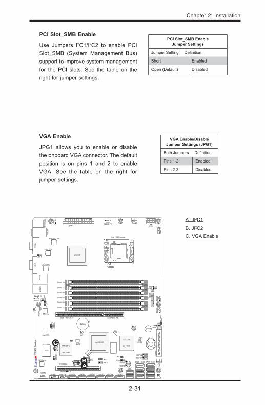
PCI Slot_SMB EnableJumper Settings
JumperSettingDefinition
Short Enabled
Open (Default) Disabled
AB
A. JI2C1
B. JI2C2
C. VGA Enable
C
VGA Enable/Disable Jumper Settings (JPG1)
BothJumpersDefinition
Pins 1-2 Enabled
Pins 2-3 Disabled
VGA Enable
JPG1 allows you to enable or disable the onboard VGA connector. The default position is on pins 1 and 2 to enable VGA. See the table on the right for jumper settings.
PCI Slot_SMB Enable
Use Jumpers I2C1/I2C2 to enable PCI Slot_SMB (System Management Bus) support to improve system management for the PCI slots. See the table on the right for jumper settings.
2-32
X8STi/X8STi-F/X8STi-3F/X8STi-LN4 User's Manual
LSI 1068E
NIC
4 LE
D
JBM
C1
A A. BP USB 0/1 Wake-up
B. FP USB 2/3, 4/5 Wake-up
C. FP USB 6, 7 Wake-up
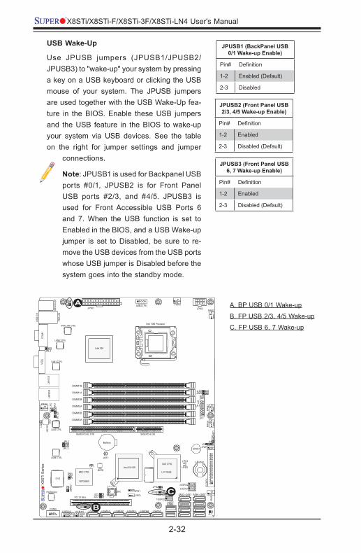
USB Wake-Up
Use JPUSB jumpers (JPUSB1/JPUSB2/JPUSB3) to "wake-up" your system by pressing a key on a USB keyboard or clicking the USB mouse of your system. The JPUSB jumpers are used together with the USB Wake-Up fea-ture in the BIOS. Enable these USB jumpers and the USB feature in the BIOS to wake-up your system via USB devices. See the table on the right for jumper settings and jumper
connections.
Note: JPUSB1 is used for Backpanel USB ports #0/1, JPUSB2 is for Front Panel USB ports #2/3, and #4/5. JPUSB3 is used for Front Accessible USB Ports 6 and 7. When the USB function is set to Enabled in the BIOS, and a USB Wake-up jumper is set to Disabled, be sure to re-move the USB devices from the USB ports whose USB jumper is Disabled before the system goes into the standby mode.
JPUSB1 (BackPanel USB 0/1 Wake-up Enable)
Pin#Definition
1-2 Enabled (Default)
2-3 Disabled
JPUSB2 (Front Panel USB 2/3, 4/5 Wake-up Enable)
Pin#Definition
1-2 Enabled
2-3 Disabled (Default)
B
C
JPUSB3 (Front Panel USB 6, 7 Wake-up Enable)
Pin#Definition
1-2 Enabled
2-3 Disabled (Default)
Chapter 2: Installation
2-33
LSI 1068E
NIC
4 LE
D
JBM
C1
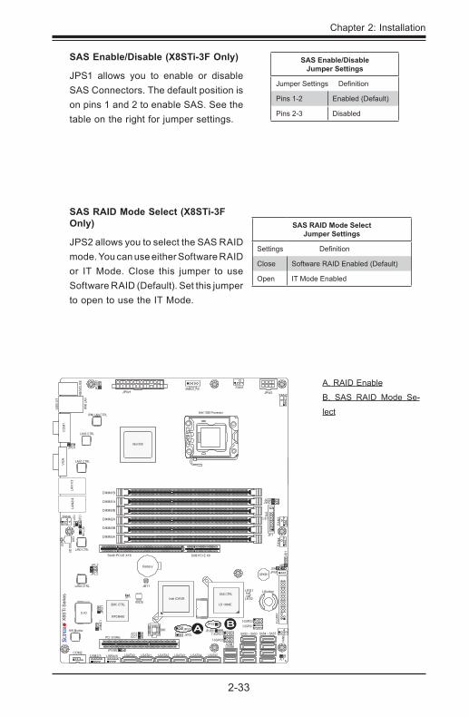
SAS Enable/Disable Jumper Settings
JumperSettingsDefinition
Pins 1-2 Enabled (Default)
Pins 2-3 Disabled
SAS Enable/Disable (X8STi-3F Only)
JPS1 allows you to enable or disable SAS Connectors. The default position is on pins 1 and 2 to enable SAS. See the table on the right for jumper settings.
SAS RAID Mode SelectJumper Settings
SettingsDefinition
Close Software RAID Enabled (Default)
Open IT Mode Enabled
SAS RAID Mode Select (X8STi-3F Only)
JPS2 allows you to select the SAS RAID mode. You can use either Software RAID or IT Mode. Close this jumper to use Software RAID (Default). Set this jumper to open to use the IT Mode.
A B
A. RAID Enable
B. SAS RAID Mode Se-
lect
2-34
X8STi/X8STi-F/X8STi-3F/X8STi-LN4 User's Manual
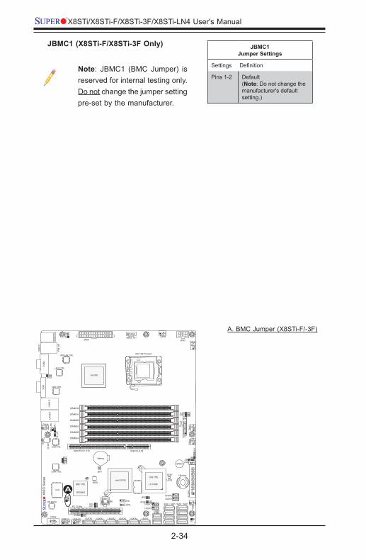
JBMC1Jumper Settings
SettingsDefinition
Pins 1-2 Default(Note: Do not change the manufacturer's default setting.)
JBMC1 (X8STi-F/X8STi-3F Only)
Note: JBMC1 (BMC Jumper) is reserved for internal testing only. Do not change the jumper setting pre-set by the manufacturer.
LSI 1068E
NIC
4 LE
D
JBM
C1
A. BMC Jumper (X8STi-F/-3F)
A
Chapter 2: Installation
2-35
LSI 1068E
NIC
4 LE
D
JBM
C1
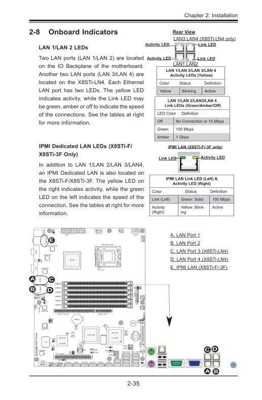
LAN 1/LAN 2 LEDs
Two LAN ports (LAN 1/LAN 2) are located on the IO Backplane of the motherboard. Another two LAN ports (LAN 3/LAN 4) are located on the X8STi-LN4. Each Ethernet LAN port has two LEDs. The yellow LED indicates activity, while the Link LED may be green, amber or off to indicate the speed of the connections. See the tables at right for more information.
2-8 Onboard Indicators
A. LAN Port 1
B. LAN Port 2
C. LAN Port 3 (X8STi-LN4)
D. LAN Port 4 (X8STi-LN4)
E. IPMI LAN (X8STi-F/-3F)
A
LAN 1/LAN 2/LAN3/LAN 4 Link LEDs (Green/Amber/Off)
LEDColorDefinition
Off No Connection or 10 Mbps
Green 100 Mbps
Amber 1 Gbps
LAN 1/LAN 2/LAN 3/LAN 4 Activity LEDs (Yellow)
ColorStatusDefinition
Yellow Blinking Active
Rear View
Activity LED
Link LED
C
B
IPMI Dedicated LAN LEDs (X8STi-F/X8STi-3F Only)
In addition to LAN 1/LAN 2/LAN 3/LAN4, an IPMI Dedicated LAN is also located on the X8STi-F/X8STi-3F. The yellow LED on the right indicates activity, while the green LED on the left indicates the speed of the connection. See the tables at right for more information.
LAN 1/LAN 2
IPMI LAN (X8ST3-F)
Link LED Activity LED
IPMI LAN (X8STi-F/-3F only)
IPMI LAN Link LED (Left) &Activity LED (Right)
ColorStatusDefinition
Link (Left) Green: Solid 100 Mbps
Activity (Right)
Yellow: Blink-ing
Active
C
LAN3 LAN4 (X8STi-LN4 only)
LAN1 LAN2Activity LED
Link LED
D
E
D
A
B
2-36
X8STi/X8STi-F/X8STi-3F/X8STi-LN4 User's Manual
LSI 1068E
NIC
4 LE
D
JBM
C1
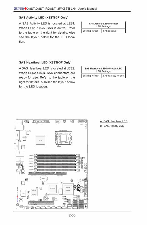
SAS Heartbeat LED (X8STi-3F Only)
A SAS Heartbeat LED is located at LES2. When LES2 blinks, SAS connectors are ready for use. Refer to the table on the right for details. Also see the layout below for the LED location.
SAS Heartbeat LED Indicator (LE5)LED Settings
Blinking: Yellow SAS is ready for use
SAS Activity LED (X8STi-3F Only)
A SAS Activity LED is located at LES1. When LES1 blinks, SAS is active. Refer to the table on the right for details. Also see the layout below for the LED loca-tion.
SAS Activity LED IndicatorLED Settings
Blinking: Green SAS is active
A
A. SAS Heartbeat LED
B. SAS Activity LED
B
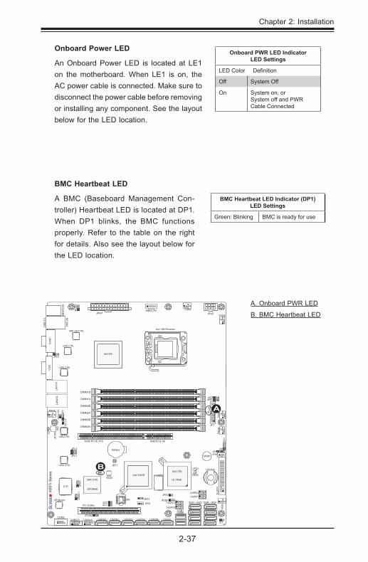
Chapter 2: Installation
2-37
LSI 1068E
NIC
4 LE
D
JBM
C1
Onboard PWR LED Indicator LED Settings
LEDColorDefinition
Off System Off
On System on, orSystem off and PWR Cable Connected
Onboard Power LED
An Onboard Power LED is located at LE1 on the motherboard. When LE1 is on, the AC power cable is connected. Make sure to disconnect the power cable before removing or installing any component. See the layout below for the LED location.
A
A. Onboard PWR LED
B. BMC Heartbeat LED
BMC Heartbeat LED
A BMC (Baseboard Management Con-troller) Heartbeat LED is located at DP1. When DP1 blinks, the BMC functions properly. Refer to the table on the right for details. Also see the layout below for the LED location.
BMC Heartbeat LED Indicator (DP1)LED Settings
Green: Blinking BMC is ready for use
B
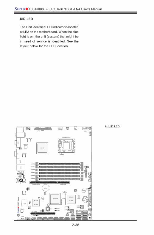
2-38
X8STi/X8STi-F/X8STi-3F/X8STi-LN4 User's Manual
UID-LED
TheUnitIdentifierLEDIndicatorislocatedat LE2 on the motherboard. When the blue light is on, the unit (system) that might be in need of service is identified. See thelayout below for the LED location.
LSI 1068E
NIC
4 LE
D
JBM
C1
A
A. UID LED
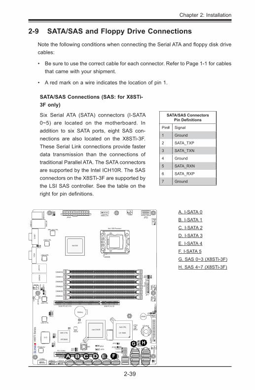
Chapter 2: Installation
2-39
LSI 1068E
NIC
4 LE
D
JBM
C1
2-9 SATA/SAS and Floppy Drive Connections
NotethefollowingconditionswhenconnectingtheSerialATAandfloppydiskdrivecables:
• Besuretousethecorrectcableforeachconnector.RefertoPage1-1forcablesthat came with your shipment.
• Aredmarkonawireindicatesthelocationofpin1.
A
SATA/SAS Connections (SAS: for X8STi-3F only)
Six Serial ATA (SATA) connectors (I-SATA 0~5) are located on the motherboard. In addition to six SATA ports, eight SAS con-nections are also located on the X8STi-3F. These Serial Link connections provide faster data transmission than the connections of traditional Parallel ATA. The SATA connectors are supported by the Intel ICH10R. The SAS connectors on the X8STi-3F are supported by the LSI SAS controller. See the table on the rightforpindefinitions.
SATA/SAS Connectors PinDefinitions
Pin# Signal
1 Ground
2 SATA_TXP
3 SATA_TXN
4 Ground
5 SATA_RXN
6 SATA_RXP
7 Ground
B
A. I-SATA 0
B. I-SATA 1
C. I-SATA 2
D. I-SATA 3
E. I-SATA 4
F. I-SATA 5
G. SAS 0~3 (X8STi-3F)
H. SAS 4~7 (X8STi-3F)
C FED
G H
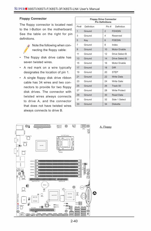
2-40
X8STi/X8STi-F/X8STi-3F/X8STi-LN4 User's Manual
LSI 1068E
NIC
4 LE
D
JBM
C1
A
A. Floppy
Floppy Connector
Thefloppyconnector is locatednextto the I-Button on the motherboard. See the table on the right for pin definitions.
Floppy Drive ConnectorPinDefinitions
Pin#DefinitionPin#Definition
1 Ground 2 FDHDIN
3 Ground 4 Reserved
5 Key 6 FDEDIN
7 Ground 8 Index
9 Ground 10 Motor Enable
11 Ground 12 Drive Select B
13 Ground 14 Drive Select B
15 Ground 16 Motor Enable
17 Ground 18 DIR
19 Ground 20 STEP
21 Ground 22 Write Data
23 Ground 24 Write Gate
25 Ground 26 Track 00
27 Ground 28 Write Protect
29 Ground 30 Read Data
31 Ground 32 Side 1 Select
33 Ground 34 Diskette
Note the following when con-nectingthefloppycable:
• The floppy disk drive cable hasseven twisted wires.
• A red mark on a wire typicallydesignates the location of pin 1.
• A single floppy disk drive ribboncable has 34 wires and two con-nectors to provide for two floppydisk drives. The connector with twisted wires always connects to drive A, and the connector that does not have twisted wires always connects to drive B.

3-1
Chapter 3: Troubleshooting
Chapter 3
Troubleshooting
3-1 Troubleshooting Procedures
Use the following procedures to troubleshoot your system. If you have followed all of the procedures below and still need assistance, refer to the ‘Technical Support Procedures’ and/or ‘Returning Merchandise for Service’ section(s) in this chapter. Always disconnect the AC power cord before adding, changing or installing any hardware components.
Before Power On1. Make sure that the Standby PWR LED (LE1) is not lit. (Note: If LE1 is on, the
onboard power is on. Be sure to unplug the power cable before installing or removing the components.)
2. Make sure that there are no short circuits between the motherboard and chas-sis.
3. Disconnect all ribbon/wire cables from the motherboard, including those for the keyboard and mouse. Also, be sure to remove all add-on cards.
4. Install a CPU and heatsink (be sure that it is fully seated) and then connect the chassis speaker and the power LED to the motherboard. Check all jumper settings as well.
No Power1. Make sure that there are no short circuits between the motherboard and chas-
sis.
2. Make sure that all jumpers are set to their default positions.
3. Check if the 115V/230V switch on the power supply is properly set.
4. Turn the power switch on and off to test the system.
5. The battery on your motherboard may be old. Check to make sure that it still supplies ~3VDC. If it does not, replace it with a new one.
No Video1. If the power is on, but you have no video--in this case, you will need to remove
alltheadd-oncardsandcablesfirst.
3-2
X8STi/X8STi-F/X8STi-3F/X8STi-LN4 User's Manual
2. Use the speaker to determine if any beep codes exist. (Refer to Appendix A for details on beep codes.)
3. Remove all memory modules and turn on the system. (If the alarm is on, check the specs of memory modules, reset the memory or try a different one.)
Memory Errors 1. Make sure that the DIMM modules are properly installed and fully seated in
the slots.
2. You should be using unbuffered ECC or non-ECC DDR3 (1.5V) 1333/1066/800 MHz memory (recommended by the manufacturer). Also, it is recommended that you use the memory modules of the same type and speed for all DIMMs in the system.
3. Check for bad DIMM modules or slots by swapping modules between slots to see if you can locate the faulty modules.
4. Check the power supply voltage 115V/230V switch.
LosingtheSystem’sSetupConfiguration1. Please be sure to use a high quality power supply. A poor quality power supply
may cause the system to lose the CMOS setup information. Refer to Section 1-5 for details on recommended power supplies.
2. The battery on your motherboard may be old. Check to verify that it still supplies ~3VDC. If it does not, replace it with a new one.
3. If the above steps do not fix the SetupConfiguration problem, contact yourvendor for repairs.
3-2 Technical Support Procedures
Before contacting Technical Support, please make sure that you have followed all the steps listed below. Also, Note that as a motherboard manufacturer, Supermicro doesnotselldirectlytoendusers,soitisbesttofirstcheckwithyourdistributororreseller for troubleshooting services. They should know of any possible problem(s) withthespecificsystemconfigurationthatwassoldtoyou.
1. Please go through the ‘Troubleshooting Procedures’ and 'Frequently Asked Question' (FAQ) sections in this chapter or see the FAQs on our website (http://www.supermicro.com/support/faqs/) before contacting Technical Support.
2. BIOS upgrades can be downloaded from our website at (http://www.supermicro.
3-3
Chapter 3: Troubleshooting
com/support/bios/).
Note: NotallBIOScanbeflashed.Somecannotbeflashed; itdependsonthemodificationstothebootblockcode.
3. If you've followed the instructions above to troubleshoot your system, and still
cannot resolve the problem, then contact Supermicro's technical support and
provide them with the following information:
•MotherboardmodelandPCBrevisionnumber
•BIOSreleasedate/version(thiscanbeseenontheinitialdisplaywhenyour
systemfirstbootsup)
•Systemconfiguration
An example of a Technical Support form is on our website at (http://www.
supermicro.com/support/contact.cfm).
4. Distributors: For immediate assistance, please have your account number ready
when placing a call to our technical support department. We can be reached
by e-mail at [email protected], by phone at: (408) 503-8000, option
2, or by fax at (408)503-8019.
3-3 Frequently Asked Questions
Question: What type of memory does my motherboard support?
Answer: The X8STi/X8STi-F/X8STi-3F/X8STi-LN4 supports up to 24 GB of unbuffered ECC or non-ECC DDR3 (1.5V) 1333/1066/800 MHz SDRAM. See Section 2-4 for details on installing memory. (Note: Both ECC and Non-ECC memory modules are supported. However, using ECC or Non-ECC memory depends on the CPU installed on the motherboard.)
Question: I installed 1333/1066 MHz memory, why doesn't my motherboard (X8SAX, C7X58, X8ST3-F/E or X8STi family) run the memory at 1333/1066 MHz?
Since the memory controller is integrated into the CPU, memory speed de-pends on the installed CPUs QPI (QuickPath Interconnect) rating. Please check your CPU specifications. For example, to support 1333 MHz memory, theCPU's QPI should be 6.4GT/S. A lower QPI number means that it will support slower memory. More information may be found at www.intel.com.
3-4
X8STi/X8STi-F/X8STi-3F/X8STi-LN4 User's Manual
Question: How do I update my BIOS?
Answer: It is recommended that you do not upgrade your BIOS if you are not experiencinganyproblemswithyoursystem.UpdatedBIOSfilesare locatedon our web site at http://www.supermicro.com/support/bios/. Please check our BIOS warning message and the information on how to update your BIOS on our website.SelectyourmotherboardmodelanddownloadtheBIOS(.rom)filetoyour computer. Also, check the current BIOS revision and make sure that it is newerthanyourBIOSbeforedownloading.Youmaychoosethezipfileorthe.exefile.IfyouchoosethezippedBIOSfile,pleaseunziptheBIOSfileontoabootabledeviceoraUSBpen/thumbdrive.Toflash theBIOS, run thebatchfilenamed"ami.bat"withthenewBIOSROMfilefromyourbootabledeviceorUSB pen/thumb drive. Use the following format:
F:\>ami.batBIOS-ROM-filename.xxx<Enter>
Notes: Always use the file named “ami.bat” to update the BIOS and inserta spacebetween "ami.bat"and thefilename. TheBIOS-ROM-filenamewillbear the motherboard name (i.e., X8STi) and build version as the extension. For example, "X8STi.115".
When completed, your system will automatically reboot. If you choose the .exe file,pleaserunthe.exefileunderWindowstocreatetheBIOSflashfloppydisk.Insert thefloppydisk into thesystemyouwish toflash theBIOS.Then,bootthesystemtothefloppydisk.TheBIOSutilitywillautomaticallyflashtheBIOSwithout any prompts. Please note that this process may take a few minutes to complete. Do not be concerned if the screen is paused for a few minutes.
Warning: Do not shut down or reset the system while updating the BIOS to prevent possible system boot failure!
WhentheBIOSflashingscreeniscompleted,thesystemwillrebootandwillshow “Press F1 or F2”. At this point, you will need to load the BIOS defaults. Press<F1>togototheBIOSsetupscreen,andpress<F9>toloadthedefaultsettings.Next,press<F10>tosaveandexit.Thesystemwillthenreboot.
Note: The SPI BIOS chip installed on this motherboard is not removable. To repair or replace a damaged BIOS chip, please send your motherboard to RMA at Supermicro for service.
Question: I think my BIOS is corrupted. How can I recover my BIOS?
Answer: Please see Appendix D, BIOS Recovery for detailed instructions.
Question: What's on the CD that came with my motherboard?
Answer: The supplied compact disc has quite a few drivers and programs that will greatly enhance your system. We recommend that you review the CD
3-5
Chapter 3: Troubleshooting
and install the applications you need. Applications on the CD include chipset drivers for Windows, security and audio drivers.
Question: I installed the RSC-R2UW-3E8 add-on card on slot 2, but the system does not detect it. How can I make it to work?
Answer: Change the option for PCIE Width to [X8X8X8]. from [X16X8] (default) intheBIOS(Advance>PCI/PnPConfiguration),thenchangetheoptionROMfor PCI-Exp Slot 2 to [Enable] from [Disable] (default).
Question: Is the PCI-Ex16 slot on X8 boards reserved for graphic cards only?
Answer: No, the PCI-Ex16 slot is not only for graphic cards. It may be used for PCI-E storage, LAN, and other peripherals.
Question: Does X8 series motherboards come with a screw type CPU heat sink bracket?
Answer: No, it does not come with a bracket for a screw-type heat sink. Cus-tomers have to purchase it separately. Please contact RMA for information, ask for part number BKT_0023L.
Question:Under theMicrosoftWindowsenvironment,howdo Iconfiguremy power button to shut-off instantly or wait 4 seconds before powering down?
Answer: Enter the BIOS Setup -> Advanced -> Boot Feature -> Power Button Function. Select "Instant Off" if you want the system to power down instantly when the power button is pressed, or select "4 Second Override" to require the power button to be pressed continuously for 4 seconds before shutting off.
3-4 Returning Merchandise for Service
A receipt or copy of your invoice marked with the date of purchase is required before any warranty service will be rendered. You can obtain service by calling your vendor for a Returned Merchandise Authorization (RMA) number. (For faster service, you may also obtain RMA authorizations online (http://www.supermicro.com/support/rma/). When returning to the manufacturer, the RMA number should be prominently displayed on the outside of the shipping carton, and mailed prepaid or hand-carried. Shipping and handling charges will be applied for all orders that must be mailed when service is complete.
This warranty only covers normal consumer use and does not cover damages incurred in shipping or from failure due to the alteration, misuse, abuse or improper maintenanceofproducts.Duringthewarrantyperiod,contactyourdistributorfirstfor any product problems.

3-6
X8STi/X8STi-F/X8STi-3F/X8STi-LN4 User's Manual
Notes
Chapter 4: AMI BIOS
4-1
Chapter 4
BIOS
4-1 Introduction
This chapter describes the AMI BIOS Setup Utility for the X8STi/X8STi-F/X8STi-3F/X8STi-LN4. The AMI ROM BIOS is stored in a Flash EEPROM and can be easily updated. This chapter describes the basic navigation of the AMI BIOS Setup Utility setup screens.
Starting BIOS Setup UtilityTo enter theAMI BIOS Setup Utility screens, press the <Delete> key while thesystem is booting up.
Note: Inmostcases, the<Delete>key isused to invoke theAMIBIOSsetup screen. There are a few cases when other keys are used, such as <F1>,<F2>,etc.
Each main BIOS menu option is described in this manual. The Main BIOS setup menu screen has two main frames. The left frame displays all the options that can beconfigured.Grayed-outoptionscannotbe configured.Options inblue canbeconfigured by the user. The right frame displays the key legend.Above the keylegend is an area reserved for a text message. When an option is selected in the left frame, it is highlighted in white. Often a text message will accompany it. (Note: the AMI BIOS has default text messages built in. Supermicro retains the option to include, omit, or change any of these text messages.)
The AMI BIOS Setup Utility uses a key-based navigation system called "hot keys". Most of the AMI BIOS setup utility "hot keys" can be used at any time during the setupnavigationprocess.Thesekeysinclude<F1>,<F10>,<Enter>,<ESC>,ar-row keys, etc.
Note: Options printed in Bold are default settings.
HowToChangetheConfigurationDataTheconfigurationdatathatdeterminesthesystemparametersmaybechangedbyentering the AMI BIOS Setup utility. This Setup utility can be accessed by pressing <Del>attheappropriatetimeduringsystemboot.
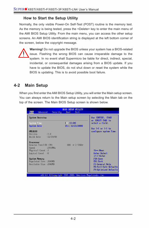
4-2
X8STi/X8STi-F/X8STi-3F/X8STi-LN4 User’s Manual
How to Start the Setup UtilityNormally, the only visible Power-On Self-Test (POST) routine is the memory test. Asthememoryisbeingtested,pressthe<Delete>keytoenterthemainmenuofthe AMI BIOS Setup Utility. From the main menu, you can access the other setup screens.AnAMIBIOSidentificationstringisdisplayedattheleftbottomcornerofthe screen, below the copyright message.
Warning! Do not upgrade the BIOS unless your system has a BIOS-related issue. Flashing the wrong BIOS can cause irreparable damage to the system. In no event shall Supermicro be liable for direct, indirect, special, incidental, or consequential damages arising from a BIOS update. If you have to update the BIOS, do not shut down or reset the system while the BIOS is updating. This is to avoid possible boot failure.
4-2 Main Setup
WhenyoufirstentertheAMIBIOSSetupUtility,youwillentertheMainsetupscreen.You can always return to the Main setup screen by selecting the Main tab on the top of the screen. The Main BIOS Setup screen is shown below.
Chapter 4: AMI BIOS
4-3
System Overview: The following BIOS information will be displayed:
System Time/System Date
Use this option to change the system time and date. Highlight System Time or Sys-tem Date using the arrow keys. Enter new values through the keyboard. Press the <Tab>keyorthearrowkeystomovebetweenfields.ThedatemustbeenteredinDay MM/DD/YY format. The time is entered in HH:MM:SS format. (Note: The time is in the 24-hour format. For example, 5:30 P.M. appears as 17:30:00.)
Supermicro X8STi/X8STi-F/X8STi-3F/X8STi-LN4
Version
Build Date
Processor
The AMI BIOS will automatically display the status of processor as shown below:
Type of Processor
Speed
Physical Count
Logical Count
System Memory
This displays the size of memory available in the system:
Populated Size
Available Size
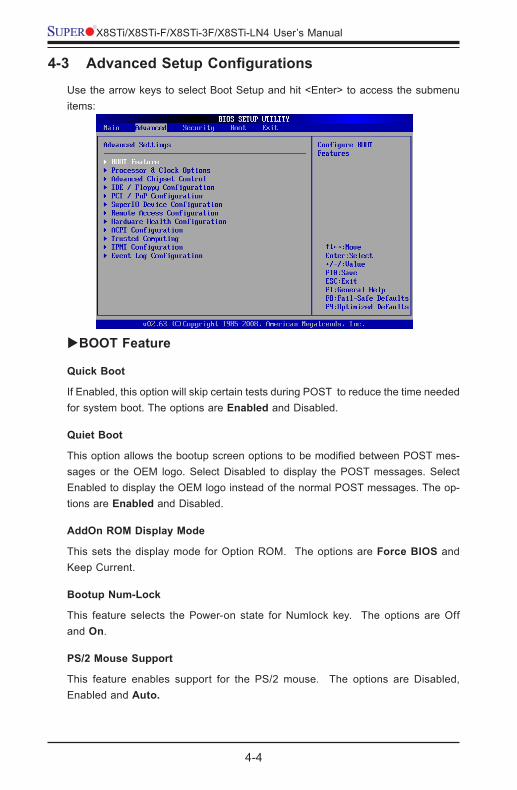
4-4
X8STi/X8STi-F/X8STi-3F/X8STi-LN4 User’s Manual
4-3 AdvancedSetupConfigurations
UsethearrowkeystoselectBootSetupandhit<Enter>toaccessthesubmenuitems:
BOOT Feature
Quick Boot
If Enabled, this option will skip certain tests during POST to reduce the time needed for system boot. The options are Enabled and Disabled.
Quiet Boot
ThisoptionallowsthebootupscreenoptionstobemodifiedbetweenPOSTmes-sages or the OEM logo. Select Disabled to display the POST messages. Select Enabled to display the OEM logo instead of the normal POST messages. The op-tions are Enabled and Disabled.
AddOn ROM Display Mode
This sets the display mode for Option ROM. The options are Force BIOS and Keep Current.
Bootup Num-Lock
This feature selects the Power-on state for Numlock key. The options are Off and On.
PS/2 Mouse Support
This feature enables support for the PS/2 mouse. The options are Disabled, Enabled and Auto.
Chapter 4: AMI BIOS
4-5
Wait For 'F1' If Error
This forces the system to wait until the 'F1' key is pressed if an error occurs. The options are Disabled and Enabled.
Hit 'Del' Message Display
This feature displays "Press DEL to run Setup" during POST. The options are Enabled and Disabled.
Watch Dog Function
If enabled, the Watch Dog Timer will allow the system to reboot when it is inactive for more than 5 minutes. The options are Enabled and Disabled.
Power Button Function
This setting allows you to decide if the power button will instantly turn the system off, or wait 4 seconds to turn off while the button is depressed. The options are 4 Seconds Override and Instant Off.
Restore on AC Power Loss
Use this feature to set the power state after a power outage. Select Power-Off for the system power to remain off after a power loss. Select Power-On for the system power to be turned on after a power loss. Select Last State to allow the system to resume its last state before a power loss. The options are Power-On, Power-Off and Last State.
Interrupt 19 Capture
Interrupt 19 is the software interrupt that handles the boot disk function. When this item is set to Enabled, the ROM BIOS of the host adaptors will "capture" Interrupt 19 at boot and allow the drives that are attached to these host adaptors to function as bootable disks. If this item is set to Disabled, the ROM BIOS of the host adap-tors will not capture Interrupt 19, and the drives attached to these adaptors will not function as bootable devices. The options are Enabled and Disabled.
Processor & Clock OptionsWarning: Take Caution when changing the Advanced settings. An incorrect value, a very high DRAM frequency or incorrect DRAM timing may cause system to become unstable. When this occurs, revert to the default setting.
CPU Ratio
This feature allows the user to use the CPU clock multiplier to multiply CPU speed in order to enhance performance. Select Manual to Manually set the multiplier set-
4-6
X8STi/X8STi-F/X8STi-3F/X8STi-LN4 User’s Manual
ting. Select Auto for the BIOS to automatically select the CPU multiplier setting for your system. The options are Auto and Manual.
Clock Spread Spectrum
Select Enable to use the feature of Clock Spectrum, which will allow the BIOS to monitor and attempt to reduce the level of Electromagnetic Interference caused by the components whenever needed. Select Disabled to enhance system stability. The options are Disabled and Enabled.
Hardware Prefetcher (Available when supported by the CPU)
If set to Enabled, the hardware pre fetcher will pre fetch streams of data and instruc-tions from the main memory to the L2 cache in the forward or backward manner to improve CPU performance. The options are Disabled and Enabled.
Adjacent Cache Line Prefetch (Available when supported by the CPU)
The CPU fetches the cache line for 64 bytes if this option is set to Disabled. The CPU fetches both cache lines for 128 bytes as comprised if Enabled.
MPS and ACPI MADT Ordering
Choose the method of ordering for the Multiple APIC Description Table (MADT). Select Modern Ordering for Microsoft Windows XP or later, Select Legacy Order-ing for Microsoft Windows 2000 or earlier. The options are Modern Ordering and Legacy Ordering.
Intel® Virtualization Technology (Available when supported by the CPU)
Select Enabled to use the feature of Virtualization Technology to allow one platform to run multiple operating systems and applications in independent partitions, creat-ing multiple "virtual" systems in one physical computer. The options are Enabled and Disabled. Note: If there is any change to this setting, you will need to power off and restart the system for the change to take effect. Please refer to Intel’s web site for detailed information.
Execute-Disable Bit Capability (Available when supported by the OS and the CPU)
Set to Enabled to enable the Execute Disable Bit which will allow the processor to designate areas in the system memory where an application code can execute andwhereitcannot,thuspreventingawormoravirusfromfloodingillegalcodesto overwhelm the processor or damage the system during an attack. The default is Enabled. (Refer to Intel and Microsoft Web Sites for more information.)
Chapter 4: AMI BIOS
4-7
Intel AES-NI (When supported by the CPU)
Intel® AES instructions are a new set of instructions available beginning with the the all new 2010 Intel® Core™ processor family based on the 32nm Intel® microarchitecture. These instructions enable fast and secure data encryption and decryption, using the Advanced Encryption Standard (AES). The options are Dis-abled and Enabled.
Simultaneous Multi-Threading (Available when supported by the CPU)
Set to Enabled to use the Hyper-Threading Technology, which will result in increased CPU performance. The options are Disabled and Enabled.
Active Processor Cores
Set to Enabled to use a processor's Second Core and beyond. (Please refer to Intel's web site for more information.) The options are All, 1 and 2.
Intel® EIST Technology
EIST (Enhanced Intel SpeedStep Technology) allows the system to automatically adjust processor voltage and core frequency in an effort to reduce power consump-tion and heat dissipation. Please refer to Intel’s web site for detailed information. The options are Disable (Disable GV3), and Enable (Enable GV3).
IntelTurboBoostConfiguration(IfsupportedbytheinstalledCPU)
Turbo Ratio Limit Program
Select Enabled to set the processor's clock ratio in relation to the bus speed. The options are Enabled and Disabled. The default value depends on the type of CPU installed. (For example, the values shown below indicate that an Intel® Core™ i7 processor 965 Extreme Edition is installed.)
1 - Core Ratio Limit
This increases (multiplies) the processor's core 1 clock speed in relation to the bus speed. The default setting is 27. Press "+" or "-" on your keyboard to change this value.
2 ~ 4 - Core Ratio Limit
This increases the processor's core 2~4 clock speeds in relation to the bus speed. The default setting is 27 for core 2 and 26 for cores 3 and 4. Press "+" or "-" on your keyboard to change this value.
TDC Limit Override
This option will override the system's default electrical current setting for the processor. The options are Enabled and Disabled.
4-8
X8STi/X8STi-F/X8STi-3F/X8STi-LN4 User’s Manual
TDC Limit Value
This option sets the processor's electrical current value. The default setting is 880. Press "+" or "-" on your keyboard to change this value.
TDP Limit Override
Select Enabled to override the default power setting for the processor. The op-tions are Enabled and Disabled.
TDP Limit Value
Use this option to set the processor's power value. The default setting is 1040. Press "+" or "-" on your keyboard to change this value.
C1E Support
SelectEnabledtousethe"EnhancedHaltState"feature.C1Esignificantlyreducesthe CPU's power consumption by reducing the CPU's clock cycle and voltage during a "Halt State." The options are Disabled and Enabled.
Intel C-STATE Tech
If enabled, C-State is set by the system automatically to either C2, C3 or C4 state. The op-tions are Disabled and Enabled.
C-State package limit setting
If set to Auto, the AMI BIOS will automatically set the limit on the C-State package register. The options are Auto, C1, C3, C6 and C7.
C1 Auto Demotion
When enabled, the CPU will conditionally demote C3, C6 or C7 requests to C1 based on un-core auto-demote information. The options are Disabled and Enabled.
C3 Auto Demotion
When enabled, the CPU will conditionally demote C6 or C7 requests to C3 based on un-core auto-demote information. The options are Disabled and Enabled.
ACPI T State
This feature Enables the ACPI throttling support for the processor to save power. The options are Disabled and Enabled.
DCA Technology
This feature accelerates the performance of TOE devices. Note: A TOE device is a special-ized, dedicated processor that is installed on an add-on card or a network card to handle some or all packet processing of this add-on card. For this motherboard, the TOE device is built inside the ESB 2 South Bridge chip. This feature is supported only by some types of processors. The options are Enabled and Disabled.
Chapter 4: AMI BIOS
4-9
DCA Prefetch Delay
A DCA Prefetch is used with TOE components to prefetch data in order to shorten execution cyclesandmaximizedataprocessingefficiency.Prefetchingtoofrequentlycansaturatethecache directory and delay necessary cache accesses. This feature reduces or increases the frequency the system prefetches data. The options are [8], [16], [24], [32], [40], [48], [56], [64], [72], [80], [88], [96], [104], [112], [120]
Advanced Chipset ControlThe items included in the Advanced Settings submenu are listed below.
QPIandIMCConfigurationQuickPath Interconnect (QPI) is the connection between the CPU and the motherboard's I/O hub. Use this feature to modify speed and power management settings.
QPI Links Speed
Use this feature to select QPI data transfer speed. The options are Slow-mode, and Full Speed.
QPI Frequency
Use this option to set the QPI frequency. The options are Auto, 4.800 GT, 5.866 GT, and 6.400 GT.
QPI L0s and L1
QuickPath Interconnect (QPI) offers three power states called L0, L0s and L1:
L0 is a normal operational state where data and control packets can be transmitted and received. All power management states are entered from this state.
L0s is intended as a power saving state. It allows a link to quickly enter and recover form a power saving state without going through recovery.
L1 is a power saving state that allows an additional power saving over L0s, but with additional resume (wake-up) latency.
Select Enabled to activate QPI power saving (L0s and L1 are automatically selected by the motherboard), select Disabled for normal operational state without any power-saving function. The options are Disabled and Enabled.
Memory Frequency
Use this option to force the system memory to run at a different frequency than the default frequency. The available options are Auto, Force DDR-800, Force DDR-1066, and Force DDR-1333.
4-10
X8STi/X8STi-F/X8STi-3F/X8STi-LN4 User’s Manual
Memory Mode
The options are Independent, Channel Mirror, Lockstep and Sparing.
Independent - All DIMMs are available to the operating system.
Channel Mirror - The motherboard maintains two identical copies of all data in memory for redundancy.
Lockstep - The motherboard uses two areas of memory to run the same set of operations in parallel.
Sparing - Memory sparing occurs when on-demand inactive memory is au-tomatically activated by the system to temporarily replace failed memory until a service action can be performed (supported only on 2010 Intel® Core™ processor family based on the 32nm Intel® microarchitecture).
Demand Scrubbing
Demand Scrubbing is a process that allows the CPU to correct correctable memory errors found on a memory module. When the CPU or I/O issues a demand-read command, and the read data from memory turns out to be a correctable error, the error is corrected and sent to the requestor (the original source). Memory is updated as well. Select Enabled to use Demand Scrub-bing for ECC memory correction. The options are Enabled and Disabled.
Patrol Scrubbing
Patrol Scrubbing is a process that allows the CPU to correct correctable memory errors detected on a memory module and send the correction to the requestor (the original source). When this item is set to Enabled, the North Bridge will read and write back one cache line every 16K cycles, if there is no delay caused by internal processing. By using this method, roughly 64 GB of memory behind the North Bridge will be scrubbed every day. The options are Enabled and Disabled.
Throttling - Closed Loop
Throttling improves reliability and reduces power in the processor by au-tomatic voltage control during processor idle states. Available options are Disabled and Enabled.
Intel VT-d
Select Enabled to enable Intel's Virtualization Technology support for Direct I/O VT-d by reporting the I/O device assignments to VMM through the DMAR ACPI Tables. This feature offers fully-protected I/O resource-sharing across the Intel platforms, providing the user with greater reliability, security and availability in networking and data-sharing. The settings are Enabled and Disabled.
Chapter 4: AMI BIOS
4-11
SR-IOV Support
Enable this item to support Single Root I/O Virtualization and Sharing (SR-IOV). The options are Disabled and Enbaled.
Intel I/OAT
TheIntelI/OAT(I/OAccelerationTechnology)significantlyreducesCPUoverheadby leveraging CPU architectural improvements, freeing resources for more other tasks. The options are Disabled and Enabled.
Active State Power Management
Select Enabled to start Active-State Power Management for signal transactions between L0 and L1 Links on the PCI Express Bus. This maximizes power-saving and transaction speed. The options are Enabled and Disabled.
Route Port 80h Cycles to
This feature allows the user to decide which bus to send debug information to. The options are Disabled, PCI and LPC.
Extend PCI Hole
Select Enabled when using a 64-bit Operating System. The options are Disabled, and Enabled.
USB Functions
This feature allows the user to decide the number of onboard USB ports to be en-abled. The Options are: Disabled, 2 USB ports, 4 USB ports, 6 USB ports, 8 USB ports, and 12 USB Ports.
USB 2.0 Controller
Select Enabled to activate the onboard USB 2.0 controller. The options are En-abled and Disabled.
Legacy USB Support
Select Enabled to use Legacy USB devices. If this item is set to Auto, Legacy USB support will be automatically enabled if a legacy USB device is installed on the motherboard, and vise versa. The settings are Disabled, Enabled and Auto.
IDE/FloppyConfigurationWhen this submenu is selected, the AMI BIOS automatically detects the presence of the IDE Devices and displays the following items:
4-12
X8STi/X8STi-F/X8STi-3F/X8STi-LN4 User’s Manual
Floppy A
Thisfeatureallowstheusertoselectthetypeoffloppydriveconnectedtothesys-tem. The options are Disabled, 360KB 5 1/4", 1.2MB 5 1/4", 720KB 3 1/2", 1.44MB 3 1/2" and 2.88MB 3 1/2".
SATA#1Configuration
If Compatible is selected, it sets SATA#1 to legacy compatibility mode, while se-lecting Enhanced sets SATA#1 to native SATA mode. The options are Disabled, Compatible, Enhanced.
ConfigureSATA#1as
This feature allows the user to select the drive type for SATA#1. The options are IDE, RAID and AHCI.
ICH RAID CodeBase (Available if RAID is selected above)
Select Intel to enable the Intel SATA Host RAID Utility. Select Adaptec to use the Adaptec Host RAID Utility. The options are Intel and Adaptec.
SATA#2Configuration(AvailableifIDEisenabledunder"ConfigureSATA#1as" above)
Selecting Enhanced will set SATA#2 to native SATA mode. The options are Disabled, Enhanced
IDE Detect Timeout (sec)
Use this feature to set the time-out value for the BIOS to detect the ATA, ATAPI devices installed in the system. The options are 0 (sec), 5, 10, 15, 20, 25, 30, and 35.
Primary IDE Master/Slave, Secondary IDE Master/Slave, Third IDE Master, and Fourth IDE Master
These settings allow the user to set the parameters of Primary IDE Master/Slave, Secondary IDEMaster/Slave,Third andFourth IDEMaster slots.Hit <Enter> toactivate the following submenu screen for detailed options of these items. Set the correctconfigurationsaccordingly.Theitemsincludedinthesubmenuare:
Type
Select the type of device connected to the system. The options are Not Installed, Auto, CD/DVD and ARMD.
LBA/Large Mode
LBA (Logical Block Addressing) is a method of addressing data on a disk drive. In the LBA mode, the maximum drive capacity is 137 GB. For drive capacities
Chapter 4: AMI BIOS
4-13
over 137 GB, your system must be equipped with a 48-bit LBA mode addressing. If not, contact your manufacturer or install an ATA/133 IDE controller card that supports 48-bit LBA mode. The options are Disabled and Auto.
Block (Multi-Sector Transfer)
Block Mode boosts the IDE drive performance by increasing the amount of data transferred. Only 512 bytes of data can be transferred per interrupt if Block Mode is not used. Block Mode allows transfers of up to 64 KB per interrupt. Select Disabled to allow data to be transferred from and to the device one sector at a time. Select Auto to allow data transfer from and to the device occur multiple sectors at a time if the device supports it. The options are Auto and Disabled.
PIO Mode
The IDE PIO (Programmable I/O) Mode programs timing cycles between the IDE drive and the programmable IDE controller. As the PIO mode increases, the cycle time decreases. The options are Auto, 0, 1, 2, 3, and 4.
Select Auto to allow the AMI BIOS to automatically detect the PIO mode. Use this value if the IDE disk drive support cannot be determined.
Select 0 to allow the AMI BIOS to use PIO mode 0. It has a data transfer rate of 3.3 MB/s.
Select 1 to allow the AMI BIOS to use PIO mode 1. It has a data transfer rate of 5.2 MB/s.
Select 2 to allow the AMI BIOS to use PIO mode 2. It has a data transfer rate of 8.3 MB/s.
Select 3 to allow the AMI BIOS to use PIO mode 3. It has a data transfer rate of 11.1 MB/s.
Select 4 to allow the AMI BIOS to use PIO mode 4. It has a data transfer band-width of 32-Bits. Select Enabled to enable 32-Bit data transfer.
DMA Mode
Select Auto to allow the BIOS to automatically detect IDE DMA mode when the IDE disk drive support cannot be determined.
Select SWDMA0 to allow the BIOS to use Single Word DMA mode 0. It has a data transfer rate of 2.1 MB/s.
Select SWDMA1 to allow the BIOS to use Single Word DMA mode 1. It has a data transfer rate of 4.2 MB/s.
Select SWDMA2 to allow the BIOS to use Single Word DMA mode 2. It has a data transfer rate of 8.3 MB/s.
4-14
X8STi/X8STi-F/X8STi-3F/X8STi-LN4 User’s Manual
Select MWDMA0 to allow the BIOS to use Multi Word DMA mode 0. It has a data transfer rate of 4.2 MB/s.
Select MWDMA1 to allow the BIOS to use Multi Word DMA mode 1. It has a data transfer rate of 13.3 MB/s.
Select MWDMA2 to allow the BIOS to use Multi-Word DMA mode 2. It has a data transfer rate of 16.6 MB/s.
Select UDMA0 to allow the BIOS to use Ultra DMA mode 0. It has a data transfer rate of 16.6 MB/s. It has the same transfer rate as PIO mode 4 and Multi Word DMA mode 2.
Select UDMA1 to allow the BIOS to use Ultra DMA mode 1. It has a data transfer rate of 25 MB/s.
Select UDMA2 to allow the BIOS to use Ultra DMA mode 2. It has a data transfer rate of 33.3 MB/s.
Select UDMA3 to allow the BIOS to use Ultra DMA mode 3. It has a data transfer rate of 44.4 MB/s.
Select UDMA4 to allow the BIOS to use Ultra DMA mode 4 . It has a data transfer rate of 66.7 MB/s.
Select UDMA5 to allow the BIOS to use Ultra DMA mode 5 . It has a data transfer rate of 100.0 MB/s.
Select UDMA6 to allow the BIOS to use Ultra DMA mode 6 . It has a data transfer rate of 133 MB/s.
The options are Auto, SWDMAn, MWDMAn, and UDMAn.
S.M.A.R.T.
Self-Monitoring Analysis and Reporting Technology (SMART) can help predict impending drive failures. Select Auto to allow the AMI BIOS to automatically de-tect hard disk drive support. Select Disabled to prevent the AMI BIOS from using the S.M.A.R.T. Select Enabled to allow the AMI BIOS to use the S.M.A.R.T. to support hard drive disk. The options are Disabled, Enabled, and Auto.
32-Bit Data Transfer
Select Enable to enable the function of 32-bit IDE data transfer. The options are Enabled and Disabled.
PCI/PnPConfigurationThis feature allows the user to set the PCI/PnP configurations for the followingitems:
Chapter 4: AMI BIOS
4-15
Clear NVRAM
This feature clears the NVRAM during system boot. The options are No and Yes.
Plug & Play OS
SelectingYesallowstheOStoconfigurePlug&Playdevices.(Thisisnotrequiredfor system boot if your system has an OS that supports Plug & Play.) Select No to allowtheAMIBIOStoconfigurealldevicesinthesystem.
PCI Latency Timer
This feature sets the latency Timer of each PCI device installed on a PCI bus. Select 64 to set the PCI latency to 64 PCI clock cycles. The options are 32, 64, 96, 128, 160, 192, 224 and 248.
PCI IDE Bus Master
When enabled, the BIOS uses PCI bus mastering for reading/writing to IDE drives. The options are Disabled and Enabled.
PCIE I/O Performance
This feature selects the setting for the IOH PCIE maximum payload size. The op-tions are 128B and 256B.
Slot 6 Width
This feature selects the bus width of the motherboard's Slot 6 PCIE slot. The options are x4x4x4x4, x8x4x4, x8x8, x16 and Auto.
ROM Scan Ordering
This item determines what kind of option ROM activates over another. The options are Onboard First and Add-on First.
Slot PCI 33MHz, PCI Slot from SXB, Slot 6 PCIE x16
Use this feature to enable or disable a PCI-E or a PCI slot. The options are Dis-abled and Enabled.
Load Onboard LAN1 Option ROM/Load Onboard LAN2 Option ROMLoad Onboard LAN3 Option ROM/Load Onboard LAN4 Option ROM (X8STi-LN4 Only)
This feature is to enable LAN OPROM for PXE. This is to boot computers using a network interface. The options are Disabled and Enabled.
4-16
X8STi/X8STi-F/X8STi-3F/X8STi-LN4 User’s Manual
Load SAS Option ROM (X8STi-3F Only)
This feature is to load the Serial Attached SCSI (SAS) option ROM, if available. The options are Disabled and Enabled.
Boot Graphics Adapter Priority
Use this feature to select the graphics controller to be used as the primary boot device. The options are Other, Onboard VGA and Slot 6. Select Slot 6 if a graphics controller is installed in the CPU-controlled Slot 6 slot.
SuperIODeviceConfiguration
Serial Port1 Address/ Serial Port2 Address
ThisoptionspecifiesthebaseI/OportaddressandtheInterruptRequestaddressof Serial Port 1 and Serial Port 2. Select Disabled to prevent the serial port from accessing any system resources. When this option is set to Disabled, the serial port physically becomes unavailable. Select 3F8/IRQ4 to allow the serial port to use 3F8 as its I/O port address and IRQ 4 for the interrupt address. The options for Serial Port1 are Disabled, 3F8/IRQ4, 2E8/IRQ3. The options for Serial Port2 are Disabled, 2F8/IRQ3, and 2E8/IRQ3.
Onboard Floppy Controller
Select Enabled to enable the onboard Floppy Controller. The options are Enabled and Disabled.
RemoteAccessConfiguration
Remote Access
This allows the user to enable the Remote Access feature. The options are Disabled and Enabled.
If Remote Access is set to Enabled, the following items will display:
Serial Port Number
This feature allows the user decide which serial port to be used for Console Redirection. The options are COM1, COM2 and COM3. An additional option, Onboard IPMI is featured on the X8STi-F/X8STi-3F motherboard only and becomes the default.
Serial Port Mode
This feature allows the user to set the serial port mode for Console Redirection. The options are 115200 8, n 1;576008,n,1;384008,n,1;192008,n,1;and9600 8, n, 1.
Chapter 4: AMI BIOS
4-17
Flow Control
ThisfeatureallowstheusertosettheflowcontrolforConsoleRedirection.Theoptions are None, Hardware, and Software.
Redirection After BIOS POST
Select Disabled to turn off Console Redirection after Power-On Self-Test (POST). Select Always to keep Console Redirection active all the time after POST. (Note: This setting may not be supported by some operating systems.) Select Boot Loader to keep Console Redirection active during POST and Boot Loader. The options are Disabled, Boot Loader, and Always.
Terminal Type
This feature allows the user to select the target terminal type for Console Redi-rection. The options are ANSI, VT100, and VT-UTF8.
VT-UTF8 Combo Key Support
A terminal keyboarddefinition thatprovidesaway tosendcommands fromaremote console. Available options are Enabled and Disabled.
Sredir Memory Display Delay
Thisfeaturedefinesthelengthoftimeinsecondstodisplaymemoryinformation.The options are No Delay, Delay 1 Sec, Delay 2 Sec, and Delay 4 Sec.
Hardware Health ConfigurationThis feature allows the user to monitor Hardware Health of the system and review the status of each item when displayed.
CPU Overheat Alarm
This option allows the user to select the CPU Overheat Alarm setting which determines when the CPU OH alarm will be activated to provide warning of possible CPU overheat.
Warning: Any temperature that exceeds the CPU threshold temperature predefinedby theCPUmanufacturermay result inCPUoverheatorsysteminstability.WhentheCPUtemperaturereachesthispredefinedthreshold,theCPU and system cooling fans will run at full speed.
The options are:
•The Early Alarm: Select this setting if you want the CPU overheat alarm (includ-ing the LED and the buzzer) to be triggered as soon as the CPU temperature reachestheCPUoverheatthresholdaspredefinedbytheCPUmanufacturer.
4-18
X8STi/X8STi-F/X8STi-3F/X8STi-LN4 User’s Manual
•The Default Alarm: Select this setting if you want the CPU overheat alarm (including the LED and the buzzer) to be triggered when the CPU temperature reaches about 5oCabovethethresholdtemperatureaspredefinedbytheCPUmanufacturer to give the CPU and system fans additional time needed for CPU and system cooling. In both the alarms above, please take immediate action as shown below. (See the notes on P. 4-18 for more information.)
CPU Temperature/System Temperature
This feature displays current temperature readings for the CPU and the System.
The following items will be displayed for your reference only:
CPU Temperature
The CPU Temperature feature will display the CPU temperature status as detected by the BIOS:
Low – This level is considered as the ‘normal’ operating state. The CPU temperature is well below the CPU ‘Temperature Tolerance’. The motherboard fans and CPU will runnormallyasconfiguredintheBIOS(FanSpeedControl).
User intervention: No action required.
Medium – The processor is running warmer. This is a ‘precautionary’ level and generally means that there may be factors contributing to this condition, but the CPU is still within its normal operating state and below the CPU ‘Temperature Tolerance’. ThemotherboardfansandCPUwillrunnormallyasconfiguredintheBIOS.Thefans may adjust to a faster speed depending on the Fan Speed Control settings.
User intervention: No action is required. However, consider checking the CPU fans and the chassis ventilation for blockage.
High – The processor is running hot. This is a ‘caution’ level since the CPU’s ‘Tem-perature Tolerance’ has been reached (or has been exceeded) and may activate an overheat alarm:
The Default Alarm – the Overheat LED and system buzzer will activate if the High condition continues for some time after it is reached. The CPU fan will run at full speed to bring the CPU temperature down. If the CPU temperature still increases even with the CPU fan running at full speed, the system buzzer will activate and the Overheat LED will turn on.
The Early Alarm – the Overheat LED and system buzzer will be activated exactly when the High level is reached. The CPU fan will run at full speed to bring the CPU temperature down.
Chapter 4: AMI BIOS
4-19
Note: In both the alarms above, please take immediate action as shown below. See CPU Overheat Alarm to modify the above alarm settings.
User intervention: If the system buzzer and Overheat LED has activated, take action immediately by checking the system fans, chassis ventilation and room temperature to correct any problems. Note: the system may shut down if it con-tinues for a long period to prevent damage to the CPU.
Notes: The CPU thermal technology that reports absolute temperatures (Celsius/Fahrenheit) has been upgraded to a more advanced feature by Intel in its newer processors. The basic concept is that each CPU is embedded by a unique temperature information that the motherboard can read. This ‘Temperature Threshold’ or ‘Temperature Tolerance’ has been assigned at the factory and is the baseline by which the motherboard takes action during different CPU temperature conditions (i.e., by increasing CPU Fan speed, triggering the Overheat Alarm, etc). Since CPUs can have different ‘Tem-perature Tolerances’, the installed CPU can now send its ‘Temperature Toler-ance’ to the motherboard resulting in better CPU thermal management.
Supermicro has leveraged this feature by assigning a temperature status to certain thermal conditions in the processor (Low, Medium and High). This makes it easier for the user to understand the CPU’s temperature status, rather than by just simply seeing a temperature reading (i.e., 25oC).
The information provided above is for your reference only. For more information on thermal management, please refer to Intel’s Web site at www.Intel.com.
IOH Temperature
This feature displays the absolute Input/Output Hub (IOH) temperature (i.e., 51oC).
System Temperature
This feature displays the absolute system temperature (i.e., 34oC).
Fan1 ~ Fan 6 Reading
This feature displays the fan speed readings from fan interfaces Fan1 through Fan5.
Fan Speed Control Modes
This feature allows the user to decide how the system controls the speeds of the onboard fans. The CPU temperature and the fan speed are correlative. When the
4-20
X8STi/X8STi-F/X8STi-3F/X8STi-LN4 User’s Manual
CPU on-die temperature increases, the fan speed will also increase for effective system cooling. Select Full Speed to allow the onboard fans to run at full speed (of 100% Pulse Width Modulation Duty Cycle) for maximum cooling. The Full Speed setting is recommended for special system configuration or debugging. SelectPerformance for the onboard fans to run at 70% of the Initial PWM Cycle for better system cooling. The Performance setting is recommended for high-power-consum-ing and high-density systems. Select Balanced for the onboard fans to run at 50% of the Initial PWM Cycle in order to balance the needs between system cooling and power saving. The Balanced setting is recommended for regular systems with normalhardwareconfigurations.SelectEnergySavingfortheonboardfanstorunat30%oftheInitialPWMCycleforbestpowerefficiencyandmaximumquietness.The Options are: Full Speed/FS (@100% of PWM Cycle), Performance/PF (@70% of PWM Cycle), Balanced/BL (@50% of PWM Cycle), and Energy Saving/ES (@30% of PWM Cycle).
Voltage Reading
This feature displays the current voltage detected of the various components in the system:
Vcore, VDIMM, 5V, 12V, -12V, 3.3Vcc, 3.3VSB, VBAT, Vtt
ACPIConfigurationUsethisfeaturetoconfigureAdvancedConfigurationandPowerInterface(ACPI)power management settings for your system.
High Performance Event Timer
Select Enabled to activate the High Performance Event Timer (HPET) that produces periodic interrupts at a much higher frequency than a Real-time Clock (RTC) does in synchronizing multimedia streams, providing smooth playback and reducing the de-pendency on other timestamp calculation devices, such as an x86 RDTSC Instruc-tion embedded in the CPU. The High Performance Event Timer is used to replace the 8254 Programmable Interval Timer. The options are Enabled and Disabled.
ACPI Aware O/S
Enable ACPI support if it is supported by the OS to control ACPI through the Operat-ing System. Otherwise, disable this feature. The options are Yes and No.
AMI OEMB Table
This enables the OEMB table support. The options are Enabled and Disabled.
Chapter 4: AMI BIOS
4-21
ACPI APIC Support
Select Enabled to include the ACPI APIC Table Pointer in the RSDT (Root System Description Table) pointer list. The options are Enabled and Disabled.
APIC ACPI SCI IRQ
When this item is set to Enabled, APIC ACPI SCI IRQ is supported by the system. The options are Enabled and Disabled.
Headless Mode
This feature is used to enable system to function without a keyboard, monitor or mouse attached The options are Enabled and Disabled.
ACPI Version Features
The options are ACPI v1.0, ACPI v2.0 and ACPI v3.0. Please refer to ACPI's website for further explanation: http://www.acpi.info/
IPMIConfiguration(X8STi-F/X8STi-3FOnly)Intelligent Platform Management Interface (IPMI) is a set of common interfaces that IT administrators can use to monitor system health and to manage the system as a whole.FormoreinformationontheIPMIspecifications,pleasevisitIntel'swebsiteat www.intel.com.
IPMI Firmware Revision
ThisitemdisplaysthecurrentIPMIfirmwarerevision.
Status of BMC
Baseboard Management Controller (BMC) manages the interface between system management software and platform hardware. This is an informational feature which returns the status code of the BMC micro controller.
View BMC System Event Log
This feature is used to view any BMC events. It shows the total number of entries and will allow the viewing of each event by scrolling down on an Entry Number and pressing Enter.
Clear BMC System Event Log
This feature is used to clear the System Event Log. Caution: Any cleared information is unrecoverable. Make absolutely sure you no longer need any data stored in the log before clearing the BMC Event Log.
4-22
X8STi/X8STi-F/X8STi-3F/X8STi-LN4 User’s Manual
SetLANConfiguration
SetthisfeaturetoconfiguretheIPMILANadapterwithanetworkaddress.
Channel Number - Enter the channel number for theSETLANConfig com-mand. This is initially set to [1]. Press "+" or "-" on your keyboard to change the Channel Number.
Channel Number Status - This feature returns the channel status for the Channel Number selected above: "Channel Number is OK" or "Wrong Channel Number".
IP Address Source - This feature selects whether the IP address, Subnet Mask and Gateway Address are automatically assigned by the network's DHCP server (DynamicHostandConfigurationProtocol)ormanuallyenteredby theuser (Static). If Static is selected, the IP Address, Subnet Mask and Gateway Address must be manually entered below. If DHCP is selected, the next three itemswillbeconfiguredautomaticallyandwillbegrayedout.TheoptionsareStatic and DHCP.
IP Address - Enter the IP address for this machine. This should be in decimal and in dotted quad form (i.e., 192.168.10.253). The value of each three-digit number separated by dots should not exceed 255.
Subnet Mask - Subnet masks tell the network which subnet this machine belongs to. The value of each three-digit number separated by dots should not exceed 255 (i.e., 255.255.255.0).
Gateway Address - Enter the Gateway address this machine will use (i.e., 192.168.10.1).
MAC Address - The BIOS will automatically enter the MAC address (also known as Hardware Address) of this machine, however it may be over-ridden. MAC addresses are 6 two-digit hexadecimal numbers (Base 16, 0 ~ 9, A, B, C, D, E, F) separated by dots. (i.e., 00.30.48.D0.D4.60)
BMC Watch Dog Timer Action
Allows the BMC to reset or power down the system if the operating system hangs or crashes. The options are Disabled, Reset System, Power Down, Power Cycle.
BMC WatchDog TimeOut [Min:Sec]
This option appears if BMC Watch Dog Timer Action (above) is enabled. This is a timed delay in minutes or seconds, before a system power down or reset after an operating system failure is detected. The options are [5 Min], [1 Min], [30 Sec], and [10 Sec].
Chapter 4: AMI BIOS
4-23
EventLogConfiguration
View Event Log
Use this option to view the System Event Log.
Mark all events as read
This option marks all events as read. The options are OK and Cancel.
Clear event log
This option clears the Event Log memory of all messages. The options are OK and Cancel.
PCIE Error Log
Use this option to enable logging of errors encountered in the system's PCIe bus. The options are Yes and No.
Memory ECC Error Log
Use this option to enable logging of errors encountered in the system's memory. The options are Yes and No.
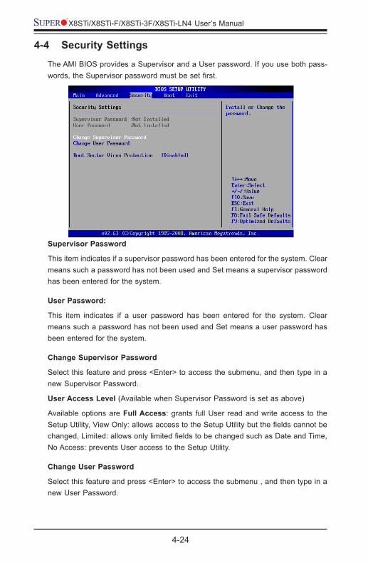
4-24
X8STi/X8STi-F/X8STi-3F/X8STi-LN4 User’s Manual
4-4 Security Settings
The AMI BIOS provides a Supervisor and a User password. If you use both pass-words,theSupervisorpasswordmustbesetfirst.
Supervisor Password
This item indicates if a supervisor password has been entered for the system. Clear means such a password has not been used and Set means a supervisor password has been entered for the system.
User Password:
This item indicates if a user password has been entered for the system. Clear means such a password has not been used and Set means a user password has been entered for the system.
Change Supervisor Password
Selectthisfeatureandpress<Enter>toaccessthesubmenu,andthentypeinanew Supervisor Password.
User Access Level (Available when Supervisor Password is set as above)
Available options are Full Access: grants full User read and write access to the SetupUtility,ViewOnly:allowsaccesstotheSetupUtilitybutthefieldscannotbechanged,Limited:allowsonlylimitedfieldstobechangedsuchasDateandTime,No Access: prevents User access to the Setup Utility.
Change User Password
Selectthisfeatureandpress<Enter>toaccessthesubmenu,andthentypeinanew User Password.
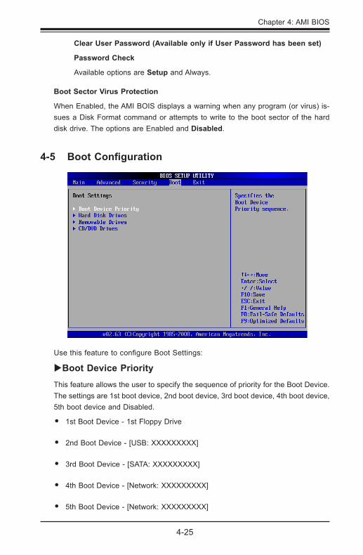
Chapter 4: AMI BIOS
4-25
UsethisfeaturetoconfigureBootSettings:
Boot Device PriorityThis feature allows the user to specify the sequence of priority for the Boot Device. The settings are 1st boot device, 2nd boot device, 3rd boot device, 4th boot device, 5th boot device and Disabled.
•1st Boot Device - 1st Floppy Drive
•2nd Boot Device - [USB: XXXXXXXXX]
•3rd Boot Device - [SATA: XXXXXXXXX]
•4th Boot Device - [Network: XXXXXXXXX]
•5th Boot Device - [Network: XXXXXXXXX]
Clear User Password (Available only if User Password has been set)
Password Check
Available options are Setup and Always.
Boot Sector Virus Protection
When Enabled, the AMI BOIS displays a warning when any program (or virus) is-sues a Disk Format command or attempts to write to the boot sector of the hard disk drive. The options are Enabled and Disabled.
4-5 BootConfiguration
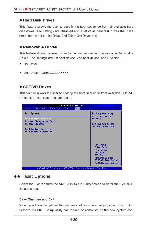
4-26
X8STi/X8STi-F/X8STi-3F/X8STi-LN4 User’s Manual
4-6 Exit Options
Select the Exit tab from the AMI BIOS Setup Utility screen to enter the Exit BIOS Setup screen.
Save Changes and Exit
When you have completed the system configuration changes, select this optionto leave the BIOS Setup Utility and reboot the computer, so the new system con-
Hard Disk DrivesThis feature allows the user to specify the boot sequence from all available hard disk drives. The settings are Disabled and a list of all hard disk drives that have been detected (i.e., 1st Drive, 2nd Drive, 3rd Drive, etc).
Removable DrivesThis feature allows the user to specify the boot sequence from available Removable Drives. The settings are 1st boot device, 2nd boot device, and Disabled.
•1st Drive
•2nd Drive - [USB: XXXXXXXXX]
CD/DVD DrivesThis feature allows the user to specify the boot sequence from available CD/DVD Drives (i.e., 1st Drive, 2nd Drive, etc).
Chapter 4: AMI BIOS
4-27
figurationparameterscantakeeffect.SelectSaveChangesandExitfromtheExitmenuandpress<Enter>.
Discard Changes and Exit
Select this option to quit the BIOS Setup without making any permanent changes tothesystemconfiguration,andrebootthecomputer.SelectDiscardChangesandExitfromtheExitmenuandpress<Enter>.
Discard Changes
Select thisoptionandpress<Enter>todiscardall thechangesandreturnto theAMI BIOS Utility Program.
Load Optimal Defaults
To set this feature, select Load Optimal Defaults from the Exit menu and press <Enter>.Then,selectOKtoallowtheAMIBIOStoautomaticallyloadOptimalDe-faults to the BIOS Settings. The Optimal settings are designed for maximum system performance, but may not work best for all computer applications.
Load Fail-Safe Defaults
To set this feature, select Load Fail-Safe Defaults from the Exit menu and press <Enter>.TheFail-Safesettingsaredesignedformaximumsystemstability,butnotfor maximum performance.

4-28
X8STi/X8STi-F/X8STi-3F/X8STi-LN4 User’s Manual
Notes
Appendix A: POST Error Beep Codes
A-1
Appendix A
POST Error Beep Codes
This section lists POST (Power On Self Test) error beep codes for the AMI BIOS. POST error beep codes are divided into two categories: recoverable and terminal. This section lists Beep Codes for recoverable POST errors.
Recoverable POST Error Beep Codes
When a recoverable type of error occurs during POST, BIOS will display a POST code that describes the problem. BIOS may also issue one of the following beep codes:
1longandeightshortbeeps-videoconfigurationerror
1 repetitive long beep - no memory detected
1 continuous beep with the front panel Overheat LED on - system overheat

A-2
X8STi/X8STi-F/X8STi-3F/X8STi-LN4 User's Manual
Notes
Appendix B: Installing the Windows OS
B-1
Appendix B
Installing the Windows OS
After allhardwarecomponentshavebeeninstalled,youmustfirstconfigureIntelSouth Bridge RAID Settings before you install the Windows OS and other software drivers.ToconfigureRAIDsettings,pleaserefertoRAIDConfigurationUserGuidesposted on our website at www.supermicro.com/support/manuals.
B-1 Installing the Windows OS to a RAID System
1. Insert Microsoft's Windows XP/2003 Setup CD in the CD Driver, and the system will start booting up from CD.
2. Pressthe<F6>keywhenthemessage-"PressF6ifyouneedtoinstallathird party SCSI or RAID driver" displays.
3. When the Windows XP/2003 Setup screen appears, press "S" to specify ad-ditional device(s).
4. Insert the driver diskette-"Intel AA RAID XP/2003 Driver for ICH10R" into DriveA:andpressthe<Enter>key.
5. Choose the Intel(R) ICH10R SATA RAID Controller from the list indicated in theXP/2003SetupScreen,andpressthe<Enter>key.
6. Pressthe<Enter>keytocontinuetheinstallationprocess.(Ifyouneedtospecify any additional devices to be installed, do it at this time.) Once all devicesarespecified,pressthe<Enter>keytocontinuewiththeinstallation.
7. FromtheWindowsXP/2003Setupscreen,pressthe<Enter>key.TheXP/2003Setupwillautomaticallyloadalldevicefilesandthen,continuetheWindows XP/2003 installation.
8. After the Windows XP/2003 OS Installation is completed, the system will auto-matically reboot.
B-2
X8STi/X8STi-F/X8STi-3F/X8STi-LN4 User's Manual Guide
B-2 Installing the Windows OS to a Non-RAID System
1. Insert Microsoft's Windows XP/2003 Setup CD in the CD Driver, and the system will start booting up from CD.
2. Pressthe<F6>keywhenthemessage-"PressF6ifyouneedtoinstallathird party SCSI or RAID driver" displays.
3. When the Windows XP/2003 Setup screen appears, press "S" to specify ad-ditional device(s).
4. InsertthedriverdisketteyouwanttoinstallintoDriveA:andpressthe<En-ter> key.
5. Pressthe<Enter>keytoproceedwiththeinstallationprocess.(Ifyouneedto specify any additional devices to be installed, do it at this time.) Once all devicesarespecified,pressthe<Enter>keytocontinuewiththeinstallation.
6. FromtheWindowsXP/2003Setupscreen,pressthe<Enter>key.TheXP/2003Setupwillautomaticallyloadalldevicefilesandthencontinuewiththe Windows XP/2003 installation.
7. After the Windows XP/2003 OS Installation is completed, the system will auto-matically reboot.
8. Insert the Supermicro Setup CD that came with your motherboard into the CD Drive during system boot, and the main screen shown on Page C-1 in Ap-pendix C will display. Follow the instructions given in Appendix C to complete software installation.
Appendix C: Software Installation Instructions
C-1
Driver/Tool Installation Display Screen
Note: Click the icons showing a hand writing on the paper to view the readmefilesforeachitem.Clickacomputericontotherightofanitemtoinstall an item (from top to the bottom) one at a time. After installing each item, you must re-boot the system before proceeding with the next item on the list. The bottom icon with a CD on it allows you to view the entire contents of the CD.
Appendix C
Software Installation Instructions
C-1 Installing Drivers
After you've installed the Windows Operating System, a screen as shown below will appear. You are ready to install software programs and drivers that have not yet been installed. To install these software programs and drivers, click the icons to the right of these items.
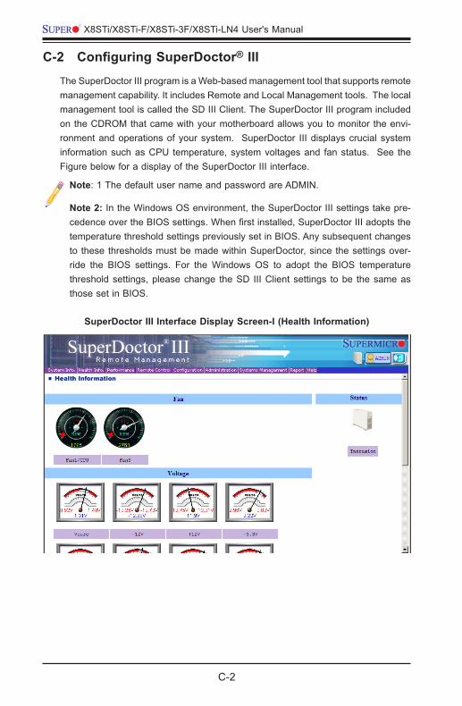
C-2
X8STi/X8STi-F/X8STi-3F/X8STi-LN4 User's Manual
SuperDoctor III Interface Display Screen-I (Health Information)
C-2 ConfiguringSuperDoctor® III
The SuperDoctor III program is a Web-based management tool that supports remote management capability. It includes Remote and Local Management tools. The local management tool is called the SD III Client. The SuperDoctor III program included on the CDROM that came with your motherboard allows you to monitor the envi-ronment and operations of your system. SuperDoctor III displays crucial system information such as CPU temperature, system voltages and fan status. See the Figure below for a display of the SuperDoctor III interface.
Note: 1 The default user name and password are ADMIN.
Note 2: In the Windows OS environment, the SuperDoctor III settings take pre-cedenceovertheBIOSsettings.Whenfirstinstalled,SuperDoctorIIIadoptsthetemperature threshold settings previously set in BIOS. Any subsequent changes to these thresholds must be made within SuperDoctor, since the settings over-ride the BIOS settings. For the Windows OS to adopt the BIOS temperature threshold settings, please change the SD III Client settings to be the same as those set in BIOS.
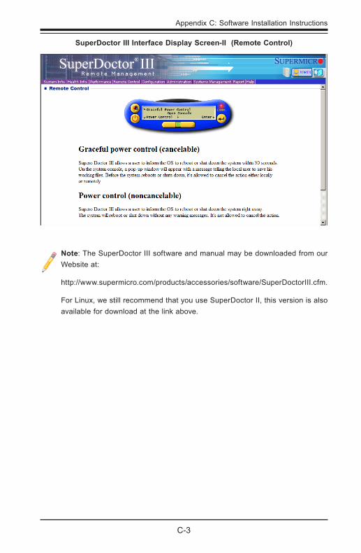
Appendix C: Software Installation Instructions
C-3
SuperDoctor III Interface Display Screen-II (Remote Control)
Note: The SuperDoctor III software and manual may be downloaded from our Website at:
http://www.supermicro.com/products/accessories/software/SuperDoctorIII.cfm.
For Linux, we still recommend that you use SuperDoctor II, this version is also available for download at the link above.

C-4
X8STi/X8STi-F/X8STi-3F/X8STi-LN4 User's Manual
Notes
Appendix D: BIOS Recovery
D-1
Appendix D - BIOS Recovery
The recovery procedure described in this section is to be used only when advised by your Supermicro Technical Support representative, or in cases of emergencies where the system no longer can boot due to a corrupted BIOS. DO NOT re-program (re-flash)theBIOSifyoursystemisrunningproperly.
D-1 Recovery Process from a USB Device/Drive (Recommended Method)
IftheBIOSfileiscorruptedandthesystemisnotabletobootup,thisfeaturewillallow you to recover the BIOS image using a USB-attached device. A USB Flash Drive or a USB CD/DVD ROM/RW drive may be used for this purpose. Please note that a USB Hard Disk drive is NOT supported at this time. Below is a two-part procedure to recover the BIOS:
Part 1: Boot Sector Recovery Process1. Using a different system, download and copy the correct BIOS binary image intoaUSBflashdeviceorawritableCD/DVDdisc'sRoot"\"Directory.Renamethedownloadedfile to "super.rom",so the recoveryprocesscan recognizeand readtheBIOSbinaryfile.
2. Insert the USB device that contains the new BIOS binary image (“super.rom”) and power the system down.
3. Whilepoweringonthesystem,pressandhold<Ctrl>and<Home>simultane-ously on your keyboard until the USB device's LED indicator comes on. This will take a few seconds or up to one minute.
4. OncetheUSBdevice'sLEDison,releasethe<Ctrl>and<Home>keys.ThesystemmaygeneratebeepcodestoindicatethattheBIOSROMfirmwareisbeingreprogrammed. The screen will also display a message as shown below. DO NOT INTERRUPT THIS PROCESS!
D-2
X8STi/X8STi-F/X8STi-3F/X8STi-LN4 User’s Manual
5. When the Boot Sector Recovery Process is complete, the system will reboot automatically and you will see a checksum error on your screen.
Part 2 - BIOS Reprogramming (Re-Flashing)After completing the Boot Sector Recovery Process, you will need to reprogram (“re-flash”)theproperBIOSbinaryfileagainintotheBIOSROMinordertohavethecorrectBIOSfile loadedbythesystem.Fordetailsonhowtoflash/re-flashaBIOS, please check our website for “Update your BIOS”, or see the section 3-3 (FAQ) of this manual. DO NOT INTERRUPT THIS PROCESS!
When completed, the system will reboot automatically, and you will see a checksum error again.
Press “F1” to go to setup. Press “F9” to load the defaults and then press “F10” to save and exit.
D-2 Recovery Process from an IDE/SATA ATAPI Disc Drive
This process is identical to the Boot Sector Recovery Process from a USB Device/Drive(asabove),exceptthattheBIOSimagefile(“super.rom”)isloadedfromanIDE/ATAPI CD/DVD/ROM/RW disc drive that is attached to the system. Note that loading from an IDE/SATA hard disk drive is NOT supported.
1. Using a different system, download and copy the correct BIOS binary image intoawritableCD/DVDdisc'sRoot "\"Directory.Rename thedownloadedfile to"super.rom", so the recovery process can recognize and read the BIOS binary file.
Note: Record/Burn the CD/DVD-R/RW disc using the ISO 9600 standard format. Refer to your CD/DVD mastering application documentation for instructions on how to do this.
2. Insert the newly-created disc into the IDE/SATA ATAPI CD/DVD ROM/RW drive of the system that has the corrupted BIOS and power the system down.
3. Follow the step-by-step instructions under Part 1 - Recovery Process from a USB Device/Drive (above) starting from Step 3 and continue on to Part 2 - BIOS Reprogramming (Re-Flashing).
If your system still does not boot up after performing the above procedure, then there may be other issues with your motherboard. Please contact your customer service representative.

(Disclaimer Continued)
The products sold by Supermicro are not intended for and will not be used in life support systems, medical equipment, nuclear facilities or systems, aircraft, aircraft devices, aircraft/emergencycommunicationdevicesorothercriticalsystemswhosefailuretoperformbereasonablyexpectedtoresultinsignificantinjuryorlossoflifeorcatastrophicproperty damage. Accordingly, Supermicro disclaims any and all liability, and should buyer use or sell such products for use in such ultra-hazardous applications, it does so entirely at its own risk. Furthermore, buyer agrees to fully indemnify, defend and hold Supermicro harmless for and against any and all claims, demands, actions, litigation, and proceedings of any kind arising out of or related to such ultra-hazardous use or sale.