Embed Size (px)
Citation preview
Wireless USB Flash Storage Device
Project Design Report
Design Team #5
Jeff Czapor
Ben Hartney
Andrew Knight
Faculty Advisor:
Dr. Ugweje
Date Submitted:
December 5, 2005

Wireless USB Project Design Report
Table of Contents
List of Figures ..................................................................................................................... ii
List of Tables ..................................................................................................................... iii
Abstract ............................................................................................................................... 1
Introduction......................................................................................................................... 2
Design Requirements .......................................................................................................... 4
Alternative Design Analysis ............................................................................................... 6
Accepted Technical Design .............................................................................................. 10
Testing Procedures............................................................................................................ 47
Financial Budget ............................................................................................................... 50
Project Schedule................................................................................................................ 52
Design Team Information ................................................................................................. 54
References......................................................................................................................... 56
i
Wireless USB Project Design Report
List of Figures
Figure 1. Adapter Module Block Diagram ...................................................................... 10
Figure 2. Storage Module Block Diagram........................................................................ 11
Figure 3. Pin-Out for the CYWUSB6934......................................................................... 13
Figure 4. Block Diagram of the CYWUSB6934 .............................................................. 14
Figure 5. CYWM6934 Block Diagram............................................................................. 14
Figure 6. Pin-Out of the USB1T20MTC .......................................................................... 17
Figure 7. The Functional Block Diagram of the PIC18F4550.......................................... 19
Figure 8. I/O Pin Assignments of the PIC18F4450 .......................................................... 20
Figure 9. The PIC USB External Interface ....................................................................... 20
Figure 10. Adapter PIC Power Connections..................................................................... 21
Figure 11. Storage PIC Power Connections ..................................................................... 22
Figure 12. Pin-out for TC58128AFT................................................................................ 25
Figure 13. Memory Cell Layout ....................................................................................... 26
Figure 14. Read Mode(l) Timing Diagram....................................................................... 26
Figure 15. Flash Memory Block Diagram ........................................................................ 27
Figure 16. Identify Initial Bad Blocks Flowchart ............................................................. 28
Figure 17. Program Flow Chart ........................................................................................ 29
Figure 18. Read Flow Chart.............................................................................................. 30
Figure 19. Erase Flow Chart ............................................................................................. 31
Figure 20. Pin-Out for MAX1874 .................................................................................... 35
Figure 21. Pin-Out for MAX8621 .................................................................................... 35
Figure 22. Pin-Out for MAX4836 .................................................................................... 36
Figure 23. Overall Software Program Under Normal Operation...................................... 38
Figure 24. Adapter Module SW Initialization Flowchart ................................................. 40
Figure 25. Storage Module SW Initialization Flowchart.................................................. 41
Figure 26. Overall Adapter Module Pseudo-Code ........................................................... 44
Figure 27. Overall Storage Module Pseudo-Code ............................................................ 45
Figure 28. Implementation Project Schedule.................................................................... 53
ii
Wireless USB Project Design Report
List of Tables
Table 1. SPI Direction and Increment............................................................................... 15
Table 2. Power Amplifier Output Power Table ................................................................ 16
Table 3. Mode Selections for USB1T20........................................................................... 18
Table 4. Power Requirements ........................................................................................... 36
Table 5. Project Budget Sheet........................................................................................... 50
Table 6. Implementation Semester Gantt Chart and Descriptions.................................... 52
iii
Wireless USB Project Design Report
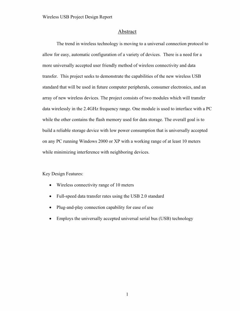
Abstract
The trend in wireless technology is moving to a universal connection protocol to
allow for easy, automatic configuration of a variety of devices. There is a need for a
more universally accepted user friendly method of wireless connectivity and data
transfer. This project seeks to demonstrate the capabilities of the new wireless USB
standard that will be used in future computer peripherals, consumer electronics, and an
array of new wireless devices. The project consists of two modules which will transfer
data wirelessly in the 2.4GHz frequency range. One module is used to interface with a PC
while the other contains the flash memory used for data storage. The overall goal is to
build a reliable storage device with low power consumption that is universally accepted
on any PC running Windows 2000 or XP with a working range of at least 10 meters
while minimizing interference with neighboring devices.
Key Design Features:
• Wireless connectivity range of 10 meters
• Full-speed data transfer rates using the USB 2.0 standard
• Plug-and-play connection capability for ease of use
• Employs the universally accepted universal serial bus (USB) technology
1
Wireless USB Project Design Report
Introduction
The overall goal of this design is to create a working flash storage device capable
of transferring data wirelessly using the USB 2.0 standard.
Statement of Need:
The trend in wireless technology is moving to a universal connection protocol to
allow for easy automatic configuration of a variety of devices. For instance, a common
need of many people is a more user-friendly method of data storage for transport between
two or more computers. The specific goal of this project is to provide a practical wireless
data storage device, demonstrating the capabilities of the USB standard that will become
an essential technology in today’s wireless lifestyle.
Problem Definition:
Goals:
● Create two separate modules with the ability to transfer data between them
wirelessly in the 2.4GHz frequency range.
● Write the embedded controller chip firmware required for Windows to detect
and enumerate the device as a usable storage drive.
● Demonstrate the wireless effectiveness of the USB 2.0 standard.
● Create a mass storage flash memory device recognized by Windows as an
accessible drive on the PC.
Objectives:
2

Wireless USB Project Design Report
● Create the USB dongle adapter capable of being inserted in to a standard
Windows 2000 or XP based PC USB port.
● Create a standalone storage device cable of transmitting and receiving data with
the PC via the USB dongle adapter.
● Effectively manage the power needs of the standalone storage device.
● Work reliably within a range of 3 meters.
Constraints:
● Must comply with FCC regulations.
● Work within the power constraints of the portable device.
● Limit compatibility to the use of Windows 2000 or XP operating systems.
● Remain within the department provided budget.
3

Wireless USB Project Design Report
Design Requirements
Wireless Communication Specifications:
The communication protocol between the two separate modules must conform to
the attributes and specifications, as stated below, of the Wireless USB set forth by
the USB Implementers Forum.
o The wired data transmission rates for the device will approach 12Mb/s,
allowing our wireless product to carry the same full-speed rate as a USB
2.0 under ideal circumstances. However, the actual radio transmission
rates will be much lower at around 62kb/s within a distance of at least 3
meters.
o Slower data rates shall also be supported where physical constraints or
multiple wireless components prohibits the data rates of the full-speed
USB 2.0 protocol.
o The radio spectrum used shall be within the unlicensed industrial,
scientific, and medical (ISM) frequency range of 2.4GHz to 2.483GHz.
The Wireless USB module should be as easily configurable and universally
accepted as its wired counterpart.
o We will restrict our design to only being compatible with Windows 2000
and Windows XP due to time constraints.
o Must have plug-and-play capabilities which will automatically install the
needed driver for use on any Windows 2000, XP machine.
Power management specifications are defined separately for each of the two
modules.
4
Wireless USB Project Design Report
o The USB dongle adapter module for the PC will be powered by the
computer’s power supply by means of the USB bus. This will be relatively
simple to implement.
Our product must also conform to applicable FCC regulations and should ensure
minimal interference with other electronic devises in the close proximity of 10
meters.
Hardware/Physical Specifications:
The USB dongle adapter module must conform to the standard physical attributes
of a typical USB port on any standard PC.
o This module must not harm or interfere with the proper operation of the
host PC. It must interface correctly with the computer by means of an
automatically created Windows driver as defined by proper
communication with the device firmware located on the microcontroller.
o This module will use the PIC18F4550 USB microcontroller along with the
Cypress CYWUSB6932 Transceiver.
The storage module which will house the flash memory storage, a battery, and a
controller PIC for transferring data wirelessly must be a completely standalone
module, meaning that it must not be connected in any way to outside sources
except through a wireless data transmission with the PCI adapter host.
o This module should fit onto a PCB no larger than 10cm by 10cm by 2cm.
o This module will use the PIC18F4550 USB microcontroller along with the
Cypress CYWUSB6932 Transceiver.
5

Wireless USB Project Design Report
Alternative Design Analysis
Introduction:
The final design has survived many changes throughout the course of the
semester. Many alternative designs resulted due to a widespread unavailability of this
extremely new technology. The proven research and necessary development support for
this new standards-based technology is simply not mature enough to be included within
the scope of the project. As stated earlier, the objective of this project was to demonstrate
the capability of this emerging wireless USB standard to work with a mass storage
peripheral device.
The design took on changes in several forms. The most important of these were
within the physical hardware interface to the PC, the transceiver parts used, and the type
of flash device used. The following sections describe these in greater detail.
General Hardware Design Alternatives:
The original adapter module design included a PC interface by means of the PCI
bus. It included a custom build PCI card which would have as its output, a standard wired
USB port and an antenna for use with the wireless communication. Because of the
complexity and strict requirements of the PCI bus specification, It was determined that it
would take too much time to implement the PCI interface for this project.
Other than the type of PC interface used, the adapter module went through several
changes throughout the design process. Most of these had to with which transceiver type
would be used to transmit the data to and from the PC bus to the storage module. After
considering many chip vendors ranging from PIC controllers to all-CMOS single solution
6
Wireless USB Project Design Report
“system on chip” (SoC) designs, it was determined that the readily available, low cost,
easy to implement PIC would be the best choice. This is described in further detail below.
The original design for the storage module has had few changes made to it. Like
the adapter module, it too went through several transceiver alternatives before settling on
the PIC for the same reasons as the adapter module. Many different chips were
considered ranging from scaled down transceivers that would require a separate
controller to expensive full-function CMOS integrated chips from vendors that advertised
them even though they were too new to be released until early to mid-year 2006. This
proved to be one of the biggest roadblocks to the design process of this project.
Controller/Transceiver Considerations:
The part of this project that took the most time to decide upon was the wireless
transceiver. There are several companies that are producing ultra-wide band transceivers
that would meet the specifications for wireless USB. Some of these transceivers were
fully integrated controllers and transceivers in one. The design was to include the
Staccato Communications transceiver. It was a single CMOS chip that had a built in
controller. The problem was the development kit for this was far more than the budget
allowed. The development kit was required to design the control software for the device
so that eliminated this transceiver. Other vendor companies that were considered were
Wisair, Alereon, and Freescale. However, the problem was typical to all of the wireless
USB transceivers simply because the technology was too new. Because of this, the
transceivers that were listed by companies that looked like realistic solutions for this
project are not yet available. All of the ultra-wideband transceivers are still under
7
Wireless USB Project Design Report
development and are in various stages of being available to the public. Since the
companies developing the transceivers do not have them working fully, this realization of
the project was abandoned. Prior to the abandonment of the ultra-wideband technology,
several companies were contacted and none of them had ultra-wideband transceivers
available. In addition the transceivers required development kits, which were usually
several thousand dollars; this too eliminated that possibility as a realistic solution for the
project.
The final decision was to use the Cypress CYWUSB6934 transceiver. This
transceiver was designed to transmit USB data for prior to the release of the wireless
USB protocol. With the ultra-wideband technology not being available, this was the best
option available. The transceiver operates in the Industrial Scientific and Medical (ISM)
portion of the frequency spectrum. While this is not in the frequency range that was
desired for the project it was decided that this transceiver would be the best option
because is was designed for wireless USB applications and since the ultra wide band
technology is not available.
The USB transceiver for the connection to the PC for both modules also took
some consideration. Ultimately the Fairchild USB1T20 was selected because it supports
USB2.0; it is also available in a TSSOP package that is easier to use. Other transceivers
were considered all were basically the same with a couple of minor differences. The main
reason the USB1T20 was selected were the convenient packaging options available.
Flash Memory Considerations:
8

Wireless USB Project Design Report
Flash Memory is the only type of memory that contains all the necessary
attributes to be used in a portable mass storage device, these attributes being non-volatile,
high density, and electrically updateable. Flash memory is offered in two technologies,
NAND and NOR. NAND type flash memory was chosen because it has faster read,
write, and erase characteristics, as well as being cheaper in price than NOR flash memory
on a bit-for-bit comparison.
Power Considerations:
It was originally considered to use a combination of 3.3V and 1.8V components
for the Storage Module. This plan was abandoned due to the increased cost and
decreased availability of 1.8V versions of components. Further, a respectable operating
life can be achieved using 3.3V components. There was no loss or gain in terms of
circuit complexity since the 1.8V components considered would have worked in
conjunction with other circuit 3.3V components.
Alternative Considerations Wrap-up:
There were several issues restricting the success of this project in terms of these
attempted design alternatives. Most of these issues came in the form of high costs, lack of
proven testing, and availability of parts. Although the original required parts were not
practically available, a valuable lesson was learned that proves that specific vendors and
parts should never be relied upon when a project is on a strict deadline with a strict
budget. Designs must always have alternative solutions available.
9
Wireless USB Project Design Report
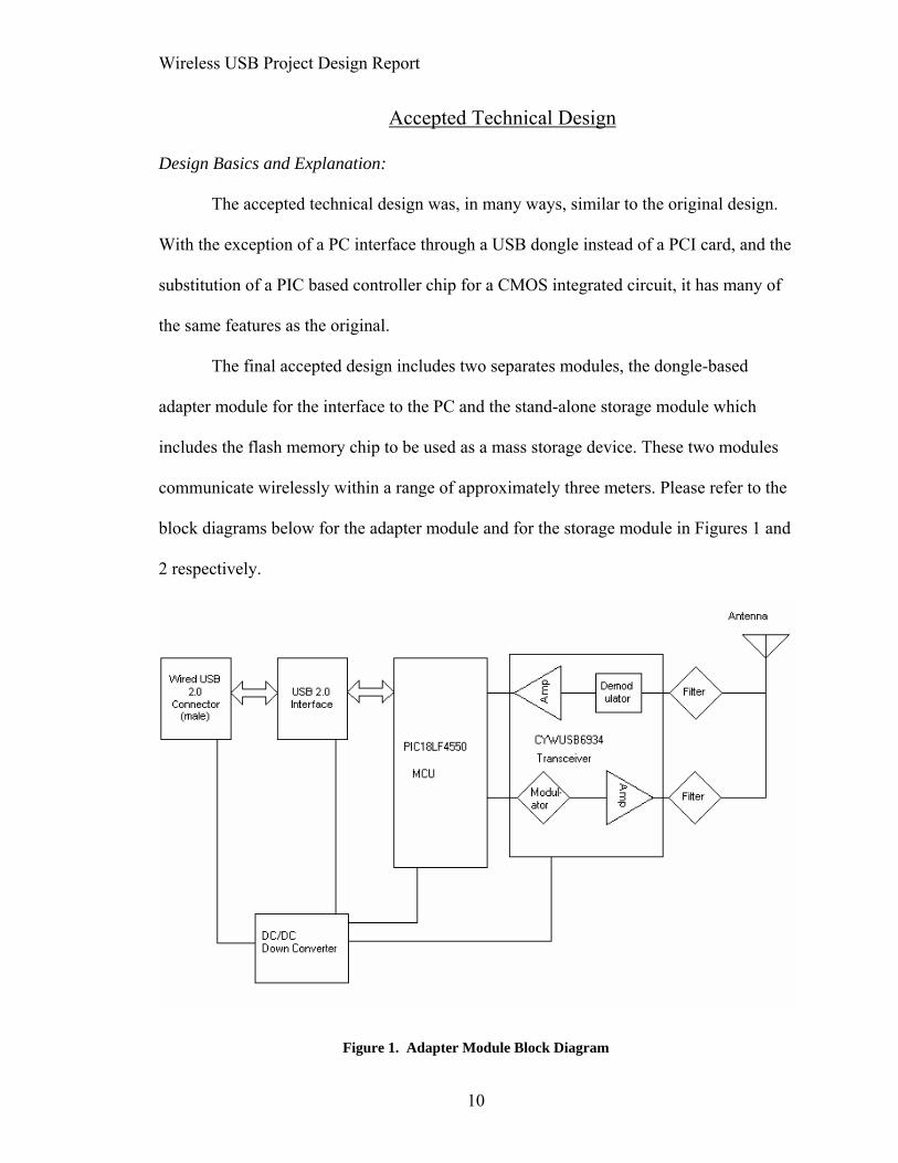
Accepted Technical Design
Design Basics and Explanation:
The accepted technical design was, in many ways, similar to the original design.
With the exception of a PC interface through a USB dongle instead of a PCI card, and the
substitution of a PIC based controller chip for a CMOS integrated circuit, it has many of
the same features as the original.
The final accepted design includes two separates modules, the dongle-based
adapter module for the interface to the PC and the stand-alone storage module which
includes the flash memory chip to be used as a mass storage device. These two modules
communicate wirelessly within a range of approximately three meters. Please refer to the
block diagrams below for the adapter module and for the storage module in Figures 1 and
2 respectively.
Figure 1. Adapter Module Block Diagram
10
Wireless USB Project Design Report
The adapter module contains the PIC18F4550 microcontroller and the Cypress wireless
USB transceiver. Other components include the USB bus power step-down converter
used to power the PIC and the transceiver, and the supporting circuitry needed for proper
operation.
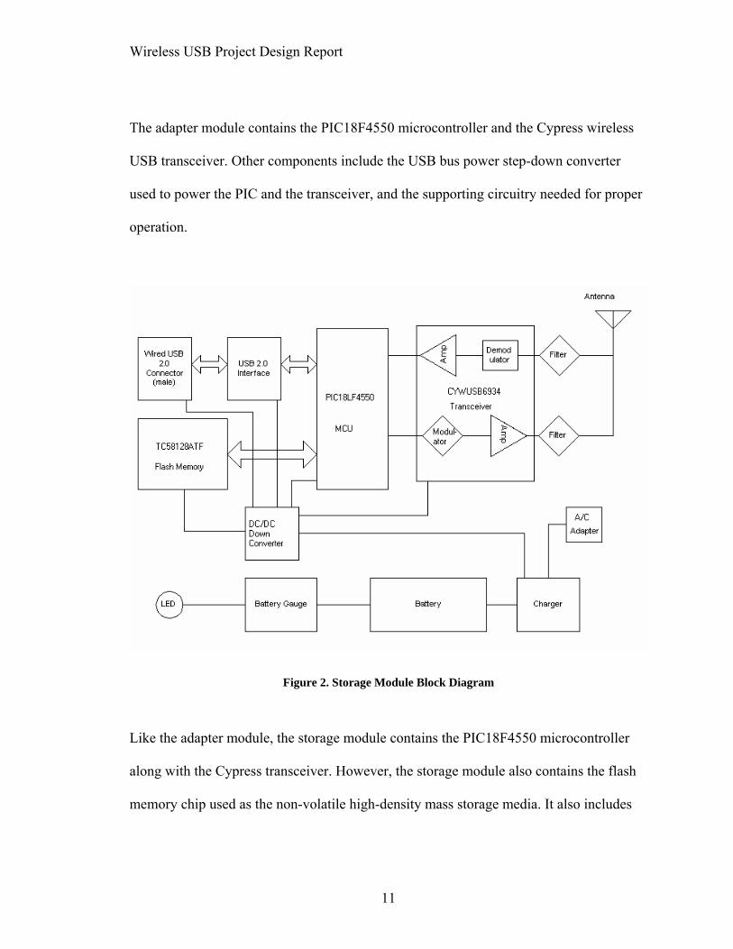
Figure 2. Storage Module Block Diagram
Like the adapter module, the storage module contains the PIC18F4550 microcontroller
along with the Cypress transceiver. However, the storage module also contains the flash
memory chip used as the non-volatile high-density mass storage media. It also includes
11
Wireless USB Project Design Report
the power circuitry needed to completely power the components of the stand-alone
storage module device.
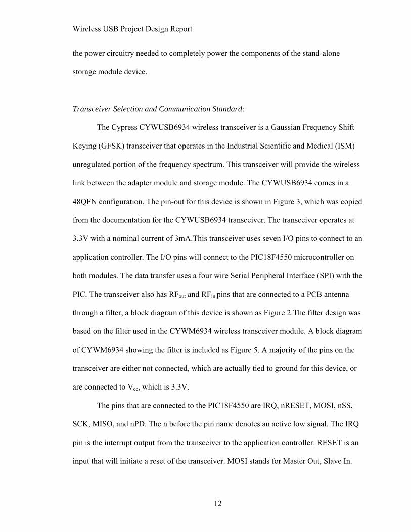
Transceiver Selection and Communication Standard:
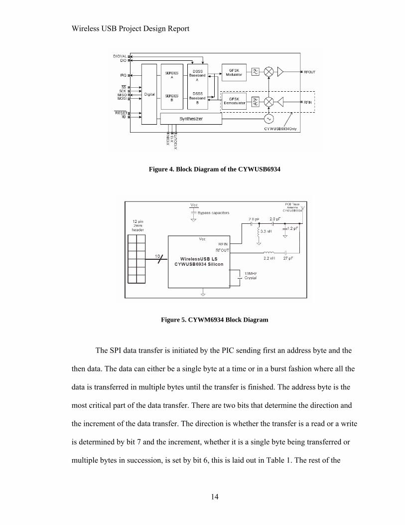
The Cypress CYWUSB6934 wireless transceiver is a Gaussian Frequency Shift
Keying (GFSK) transceiver that operates in the Industrial Scientific and Medical (ISM)
unregulated portion of the frequency spectrum. This transceiver will provide the wireless
link between the adapter module and storage module. The CYWUSB6934 comes in a
48QFN configuration. The pin-out for this device is shown in Figure 3, which was copied
from the documentation for the CYWUSB6934 transceiver. The transceiver operates at
3.3V with a nominal current of 3mA.This transceiver uses seven I/O pins to connect to an
application controller. The I/O pins will connect to the PIC18F4550 microcontroller on
both modules. The data transfer uses a four wire Serial Peripheral Interface (SPI) with the
PIC. The transceiver also has RFout and RFin pins that are connected to a PCB antenna
through a filter, a block diagram of this device is shown as Figure 2.The filter design was
based on the filter used in the CYWM6934 wireless transceiver module. A block diagram
of CYWM6934 showing the filter is included as Figure 5. A majority of the pins on the
transceiver are either not connected, which are actually tied to ground for this device, or
are connected to Vcc, which is 3.3V.
The pins that are connected to the PIC18F4550 are IRQ, nRESET, MOSI, nSS,
SCK, MISO, and nPD. The n before the pin name denotes an active low signal. The IRQ
pin is the interrupt output from the transceiver to the application controller. RESET is an
input that will initiate a reset of the transceiver. MOSI stands for Master Out, Slave In.
12
Wireless USB Project Design Report
This is the data signal from the PIC to the transceiver module. SS is an active low slave
select signal. This is an input signal from the PIC and it enables the SPI data transfer. It
must be active through the entire data transfer. SCK is a clock input from the PIC that
allows the data transfer to be synchronized properly. MISO stands for Master In, Slave
Out. This pin is used to transfer data from the transceiver to the PIC. The last pin is the
PD pin. This is the Power down pin. It too is active low and when it is asserted the
transceiver module will power itself down. The DIOVAL and DIO pins are for SERDES
(Serializer/ Deserializer), which will not be used for this project so they will be left
unconnected They are shown in Figure two at the two inputs at the top of the block
diagram. X13OUT, which is an output 13MHZ clock signal, is also not needed for this
project.
Figure 3. Pin-Out for the CYWUSB6934
13
Wireless USB Project Design Report
Figure 4. Block Diagram of the CYWUSB6934
Figure 5. CYWM6934 Block Diagram
The SPI data transfer is initiated by the PIC sending first an address byte and the
then data. The data can either be a single byte at a time or in a burst fashion where all the
data is transferred in multiple bytes until the transfer is finished. The address byte is the
most critical part of the data transfer. There are two bits that determine the direction and
the increment of the data transfer. The direction is whether the transfer is a read or a write
is determined by bit 7 and the increment, whether it is a single byte being transferred or
multiple bytes in succession, is set by bit 6, this is laid out in Table 1. The rest of the
14

Wireless USB Project Design Report
address byte is 6 bits that are the address for the actual data transfer. Once the address
byte has been sent the data is then transferred according to the procedure selected by bits
6 and 7. If the increment is set to 1 then the transceiver will automatically increment the
address by one after each byte is sent.
Table 1. SPI Direction and Increment
Bit 7 6 Bit name Direction Increment Result
Value 0 0 Single Byte Read Value 0 1 Burst Read Value 1 0 Single Byte write Value 1 1 Burst write
The wireless transceiver will be controlled entirely through software on the PIC
microcontroller. The transceiver is available in another package, the CYWM6934, which
includes the entire circuit board including the antenna. This device takes the 48 pin
transceiver circuit and lays out all of the circuitry and then gives a 12 pin header. This is
the device that will be used for the project. The general layout of the board is shown in
Figure 4. The twelve pins are the seven I/O pins, Vcc, two ground pins, and two pins are
left unconnected.
The output power can also be controlled on this transceiver. There are two ways
to control the power first is using the PACTL pin (34) on the transceiver the other is by
setting the register for output power. The power is changed to one of eight settings
corresponding to two bits for the register. The corresponding output powers are listed in
Table 2. The default power amplifier setting is ‘0’ which is –29.0dBm, this is the setting
that will be used for the project, unless additional power is needed. The transceiver was
designed in compliance with FCC regulations and also is compliant with European,
15

Wireless USB Project Design Report
Canadian and Japanese regulations. With a minimum receiver sensitivity of –90dBm the
transceiver pair will be able to communicate at a range of about 10m.
Table 2. Power Amplifier Output Power Table
The USB1T20 USB transceiver component is used to connect the modules to the
PC through a wired interface. The USB1T20 is a USB2.0 transceiver capable of full
speed data transfer at 12Mbps. This device runs at Vcc of 3.3V with a maximum input
current of 100mA. This is a 14-pin device that is used to properly communicate to the PC
through the Universal Serial Bus (USB), the pin-out is included as Figure 4. This will be
the link that interfaces the PIC microcontroller to the PC. The transceiver is connected
directly to the D+, D- through 24kΩ +/-1% resistors. There is also a filter circuit
consisting of a 300pF capacitor and a 1.5 kΩ resistor connecting D- to ground to handle
the low speed AC characteristics of the USB transfer.
16

Wireless USB Project Design Report
Figure 6. Pin-Out of the USB1T20MTC
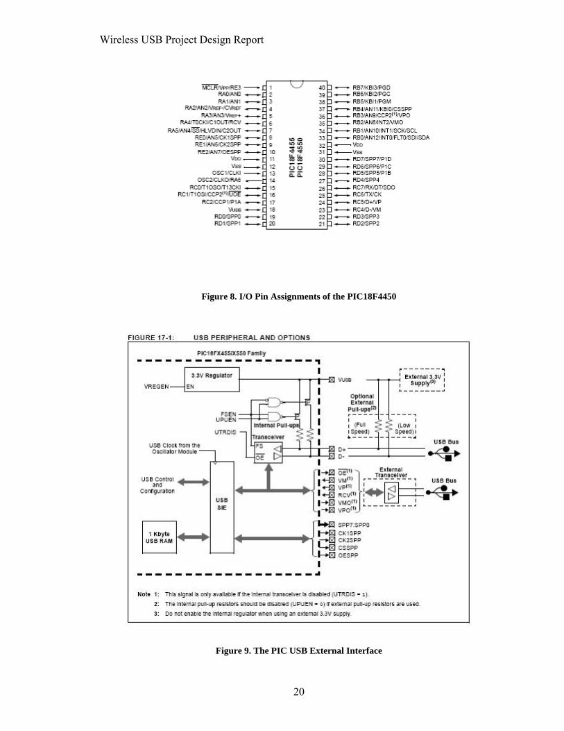
The connections to the PIC are MODE, OE, RCV, Vp, Vm, SUSPND, SPEED,
Vpo, and Vmo. Mode is a mode selection bit. It determines two different truth tables for
interpreting incoming data on the Vpo, and Vmo lines. Table 3 shows the truth tables for
MODE. From the table if MODE is set to ‘0’ then the logic ‘1’ and ‘0’ are based on the
state of Vpo, and an error occurs if Vmo is a ‘1’. When Mode set to ‘1’ the operation mode
is that the two must be different and Vpo determines the logic level. When both bits are
‘0’ and error occurs and both being a ‘1’ is classified as an illegal code. Vpo and Vmo are
the data inputs from the PIC. OE is an active low signal it is an input from the PIC that
allows data to be transmitted to the serial bus. RCV is and output that is high when data is
being received. Vp, and Vm are the data outputs to the PIC. They are gated versions of D+
and D-, the data transfer lines for USB. It is also used to detect Single Ended Zero errors
and also transmits the interconnection speed. The SUSPND pin denoted the suspend
input. When this pin is driven high the transceiver will be placed into a low power use
suspend mode. When this occurs the two data lines to the serial bus are set to state 3,
which is a high impedance setting. The final connection to the PIC is the SPEED pin, this
is and input from the PIC and is the speed selection for the data transfer across the serial
17
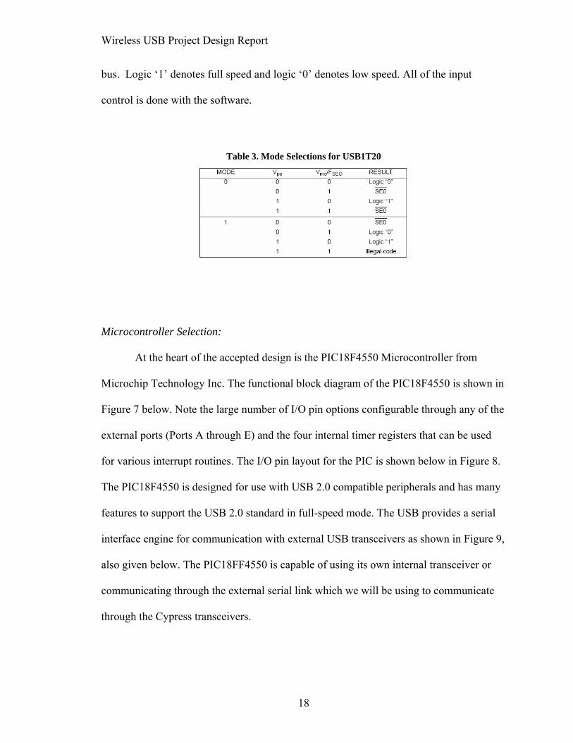
Wireless USB Project Design Report
bus. Logic ‘1’ denotes full speed and logic ‘0’ denotes low speed. All of the input
control is done with the software.
Table 3. Mode Selections for USB1T20
Microcontroller Selection:
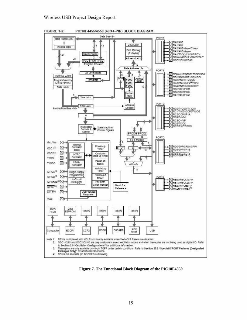
At the heart of the accepted design is the PIC18F4550 Microcontroller from
Microchip Technology Inc. The functional block diagram of the PIC18F4550 is shown in
Figure 7 below. Note the large number of I/O pin options configurable through any of the
external ports (Ports A through E) and the four internal timer registers that can be used
for various interrupt routines. The I/O pin layout for the PIC is shown below in Figure 8.
The PIC18F4550 is designed for use with USB 2.0 compatible peripherals and has many
features to support the USB 2.0 standard in full-speed mode. The USB provides a serial
interface engine for communication with external USB transceivers as shown in Figure 9,
also given below. The PIC18FF4550 is capable of using its own internal transceiver or
communicating through the external serial link which we will be using to communicate
through the Cypress transceivers.
18
Wireless USB Project Design Report
Figure 7. The Functional Block Diagram of the PIC18F4550
19
Wireless USB Project Design Report
Figure 8. I/O Pin Assignments of the PIC18F4450
Figure 9. The PIC USB External Interface
20
Wireless USB Project Design Report
The PIC18F4550 was chosen for its versatility, low cost and ease of
implementation. It has 2048 bytes of RAM, is capable of transmitting at 12MBits/s as
required for full speed USB operation, has 1024 bytes available for USB buffer, and runs
at a max speed of 48MHz. Although the low power version of this same PIC (the
PIC18lF4550) will be used for the storage module, no distinction will be made between
the two chips because they are essentially the same die and are functionally the same
chip. The difference is that the low power chip is specifically tested for lower power
inputs.
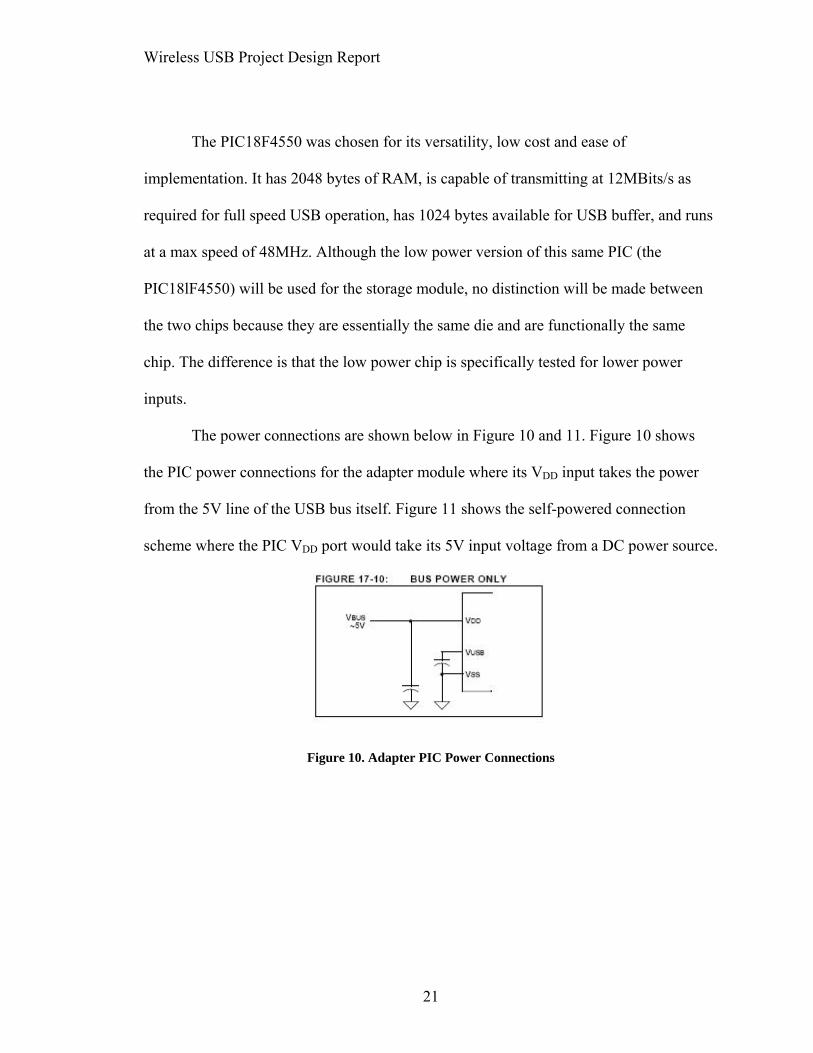
The power connections are shown below in Figure 10 and 11. Figure 10 shows
the PIC power connections for the adapter module where its VDD input takes the power
from the 5V line of the USB bus itself. Figure 11 shows the self-powered connection
scheme where the PIC VDD port would take its 5V input voltage from a DC power source.
Figure 10. Adapter PIC Power Connections
21

Wireless USB Project Design Report
Figure 11. Storage PIC Power Connections
There are some additional features of the PIC18F4550 specific to the control
operation, interrupts, and timer registers associated with USB devices. The USB specific
registers that are of particular importance are the USB Control Register (UCON), the
USB Configuration register (UCFG), and the USB Status Register (USTAT). For the
interrupt structures, four more registers are available for use. These are the interrupt
status (UIR), interrupt enable (UIE), error interrupt status (UEIR), and error interrupt
enable (UEIE) registers.
The PIC also supports many commands useful to the mass storage device
peripheral USB operation. It provides for various data transfer types that are required for
this type of device. For USB 2.0, command, interrupt, and bulk transfer will be used to
transfer data with the PC USB Host. Bulk and interrupt transfers will be of special
importance to the device due to the need to transfer a large number of data packets at a
single time, and the need for interrupts to handle user interaction and system level
computation trade-offs.
Flash Memory:
22

Wireless USB Project Design Report
Flash memory is electrically updateable (stored data can be erased and replaced
under system processor control), high density, and non-volatile (retains data stored to it
when powered off). It is used to provide the mass storage on the storage module. The
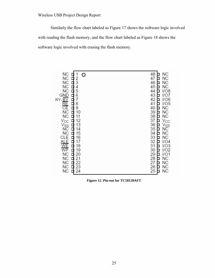
Toshiba TC58128AFT Flash Memory chosen is a single 3.3V 128M-bit NAND Flash
Memory. It comes in a TSOPI48 package with the pin-out shown in Figure 12. Figure
15 shows a block diagram of the Flash IC. The Flash uses an eight-pin I/O data bus, six
logic input pins, one output pin that shows if the device is ready or busy, and power
supply pins.
The basic concept of how a flash memory cell works is rather simple. Storing
electrons on a floating gate changes the stored cell data from a one to a zero. The
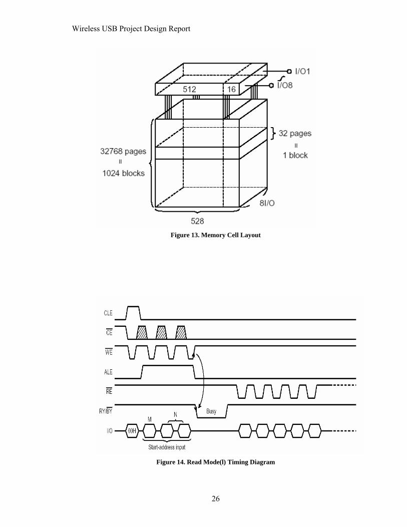
memory array of the Toshiba TC58128AFT is organized in 1024 blocks where each
block contains 32 pages. Each page is split into a main area with two half pages of 256
bytes each that are used to store the data, and a spare area of 16 bytes that is used to store
Error Correction Codes and Bad Block identification. A visual representation of this cell
layout is shown in Figure 13.
There are nine possible operations for the flash. They are Serial Data Input, Read
mode 1, Read mode 2, Read Mode 3, Reset, Auto Program, Auto Block Erase, Status
Read, and ID Read. Performing any operation involves precisely timed high and low
inputs on the six logic input pins, in combination with commands sent over the eight I/O
pins at there appropriate time in correspondence to the state of the logic pins. Data is
then read or written over the eight I/O pins. Pages of detailed timing diagrams are
supplied in the Toshiba Flash data sheets to perform the operations and possible
variations of the operations. For lack of space required to cover all these operations in
23

Wireless USB Project Design Report
detail, only the read mode1 will be covered. Figure 14 shows the timing diagram for a
read mode(1), which is a read that starts in the first half of a page.
Referencing Figure 14, first the Command Latch Enable (CLE) is driven high to
load a command, and the Chip Enable (CE) is driven low to bring the Flash out of
Standby. The 00H command is then written over the I/O pins and the Write Enable (WE)
is cycled, because the Flash reads the command on its rising edge. Next the Address
Latch Enable (ALE) is driven high, and three values specifying a starting address are
entered over the I/O pins over three cycles of the Write Enable (WE) pin. Now the ALE
pin is driven low again and the Read Enable (RE) pin is cycled. Data is available to read
35nS after a falling edge on the RE pin. The RE pin can be cycled as many times as
needed to read the desired amount of data. The other operations follow a similar scheme.
The microcontroller, in addition to performing an operation, must verify that the
operation was successful. Figures 15 through 18 show the flow charts the software
follows when performing an operation.
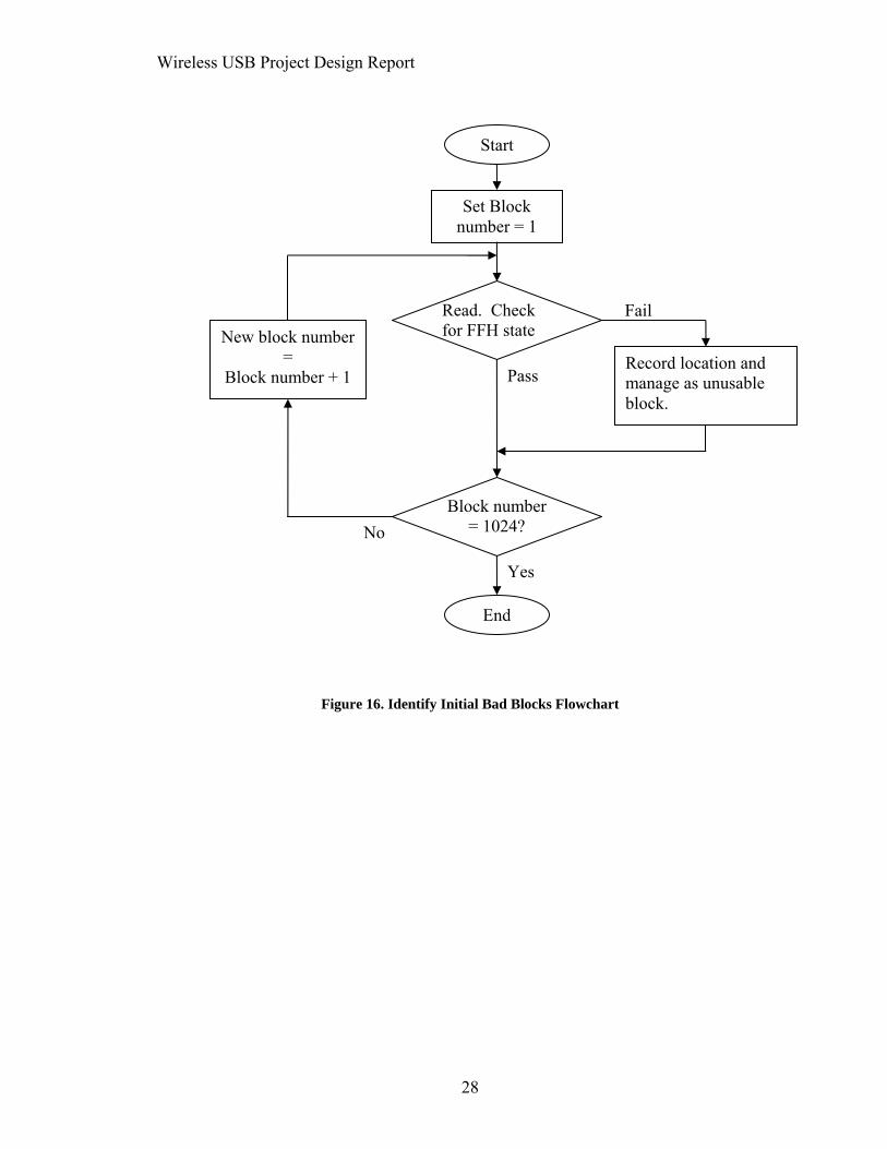
Figure 15 shows the Identifying Initial Bad Blocks flowchart. NAND flash
typically contains a number of bad blocks from the factory. The flash memory is
installed in to the system and the routine shown in Figure 15 is run by the microprocessor
to record the locations of the bad blocks so they can be recorded and managed.
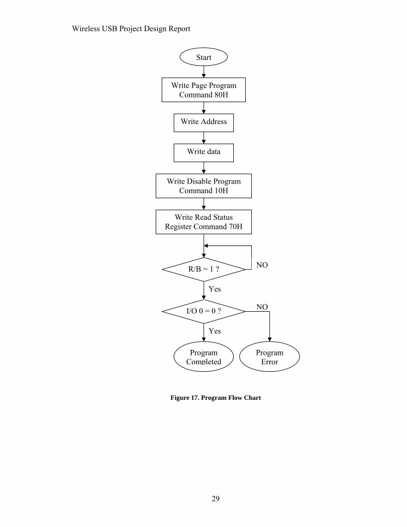
The flow chart labeled as Figure 16 shows the software logic involved with
programming the flash memory. The page program command is written, the starting
address specified, the desired amount of data is written, and the program command is
disabled. Then the microcontroller verifies the data by reading the status register and
determines if the program was successfully written.
24
Wireless USB Project Design Report
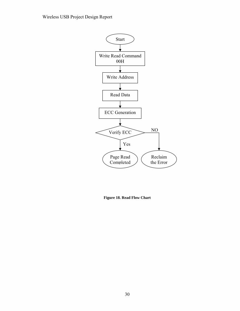
Similarly the flow chart labeled as Figure 17 shows the software logic involved
with reading the flash memory, and the flow chart labeled as Figure 18 shows the
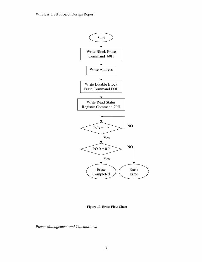
software logic involved with erasing the flash memory.
Figure 12. Pin-out for TC58128AFT
25
Wireless USB Project Design Report
Figure 13. Memory Cell Layout
Figure 14. Read Mode(l) Timing Diagram
26
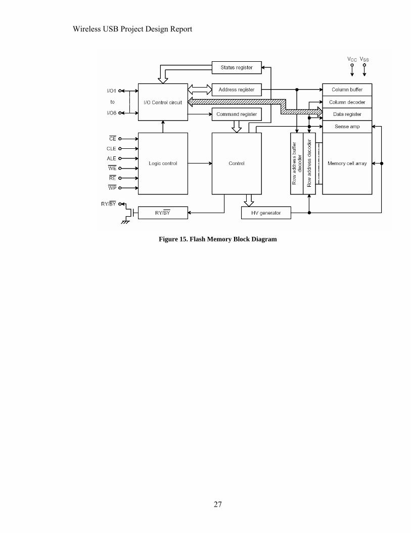
Wireless USB Project Design Report
Figure 15. Flash Memory Block Diagram
27
Wireless USB Project Design Report
Fail
Pass
Yes
No
Set Block number = 1
Start
End
Block number = 1024?
Read. Check for FFH state New block number
= Block number + 1
Record location and manage as unusable block.
Figure 16. Identify Initial Bad Blocks Flowchart
28
Wireless USB Project Design Report
NO
Write Page Program Command 80H
Yes
Start
I/O 0 = 0 ?
R/B = 1 ?
Write Read Status Register Command 70H
Write Disable Program Command 10H
Write data
Write Address
Yes
NO
Program Error
Program Completed
Figure 17. Program Flow Chart
29
Wireless USB Project Design Report
NO
Write Read Command 00H
Yes
Start
Verify ECC
ECC Generation
Read Data
Write Address
Reclaim the Error
Page Read Completed
Figure 18. Read Flow Chart
30
Wireless USB Project Design Report
NO
NO
Write Block Erase Command 60H
Yes
Start
I/O 0 = 0 ?
R/B = 1 ?
Write Read Status Register Command 70H
Write Disable Block Erase Command D0H
Write Address
Yes
Erase Error
Erase Completed
Figure 19. Erase Flow Chart
Power Management and Calculations:
31
Wireless USB Project Design Report
The power management circuit of the portable flash drive is required to provide
3.3V power to the flash memory and microprocessor when plugged directly in to a USB
port, or provide power to the flash memory, microprocessor, and transceiver when used
wirelessly. The power management circuit is built around two IC chips, the MAX1874
and the MAX8621, both manufactured by the Maxim division of Dallas Semiconductor.
The function of the MAX1874 is to control the charging current from a USB port
or an AC adapter to the Lithium Ion battery based on the charging limitations of the
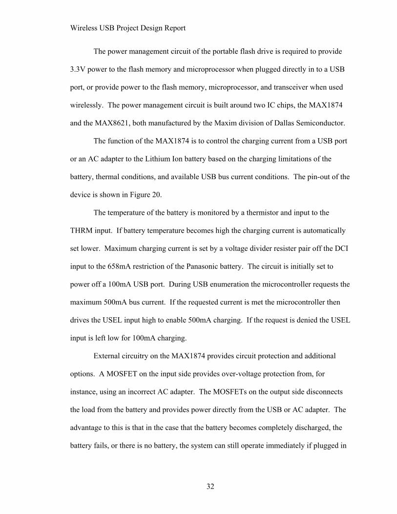
battery, thermal conditions, and available USB bus current conditions. The pin-out of the
device is shown in Figure 20.
The temperature of the battery is monitored by a thermistor and input to the
THRM input. If battery temperature becomes high the charging current is automatically
set lower. Maximum charging current is set by a voltage divider resister pair off the DCI
input to the 658mA restriction of the Panasonic battery. The circuit is initially set to
power off a 100mA USB port. During USB enumeration the microcontroller requests the
maximum 500mA bus current. If the requested current is met the microcontroller then
drives the USEL input high to enable 500mA charging. If the request is denied the USEL
input is left low for 100mA charging.
External circuitry on the MAX1874 provides circuit protection and additional
options. A MOSFET on the input side provides over-voltage protection from, for
instance, using an incorrect AC adapter. The MOSFETs on the output side disconnects
the load from the battery and provides power directly from the USB or AC adapter. The
advantage to this is that in the case that the battery becomes completely discharged, the
battery fails, or there is no battery, the system can still operate immediately if plugged in
32
Wireless USB Project Design Report
to an USB or AC adapter, rather than having to wait for the battery to charge, or not
being capable of operating at all. The four diodes prevent reverse feeding to the USB and
AC inputs.
The Bi-color LED is used as a charging gauge. It is powered red when plugged in
to a USB or AC adapter power source through a MOSFET. When charging is complete
the CHG output from the MAX1874 is driven high and the red LED is turned off and the
green LED is turned on through a pair of MOSFET’s.
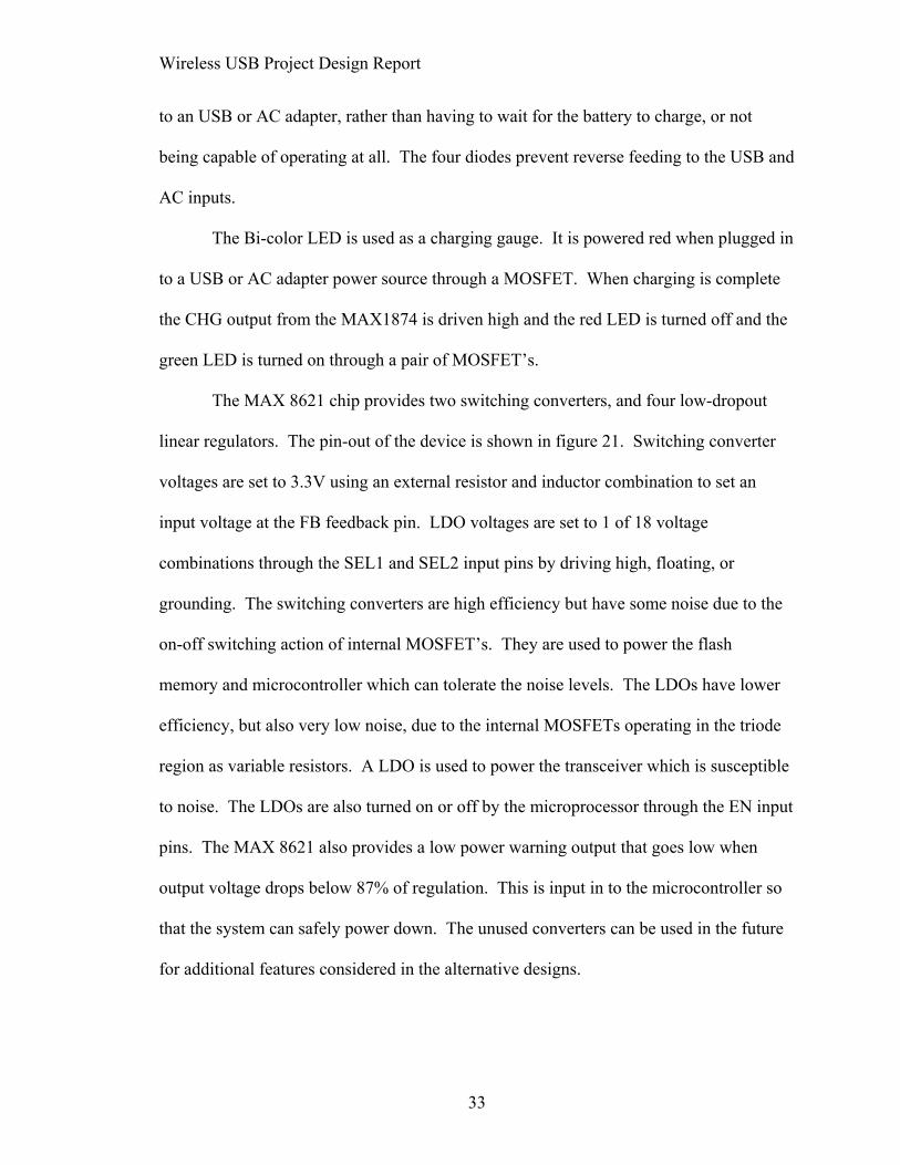
The MAX 8621 chip provides two switching converters, and four low-dropout
linear regulators. The pin-out of the device is shown in figure 21. Switching converter
voltages are set to 3.3V using an external resistor and inductor combination to set an
input voltage at the FB feedback pin. LDO voltages are set to 1 of 18 voltage
combinations through the SEL1 and SEL2 input pins by driving high, floating, or
grounding. The switching converters are high efficiency but have some noise due to the
on-off switching action of internal MOSFET’s. They are used to power the flash
memory and microcontroller which can tolerate the noise levels. The LDOs have lower
efficiency, but also very low noise, due to the internal MOSFETs operating in the triode
region as variable resistors. A LDO is used to power the transceiver which is susceptible
to noise. The LDOs are also turned on or off by the microprocessor through the EN input
pins. The MAX 8621 also provides a low power warning output that goes low when
output voltage drops below 87% of regulation. This is input in to the microcontroller so
that the system can safely power down. The unused converters can be used in the future
for additional features considered in the alternative designs.
33
Wireless USB Project Design Report
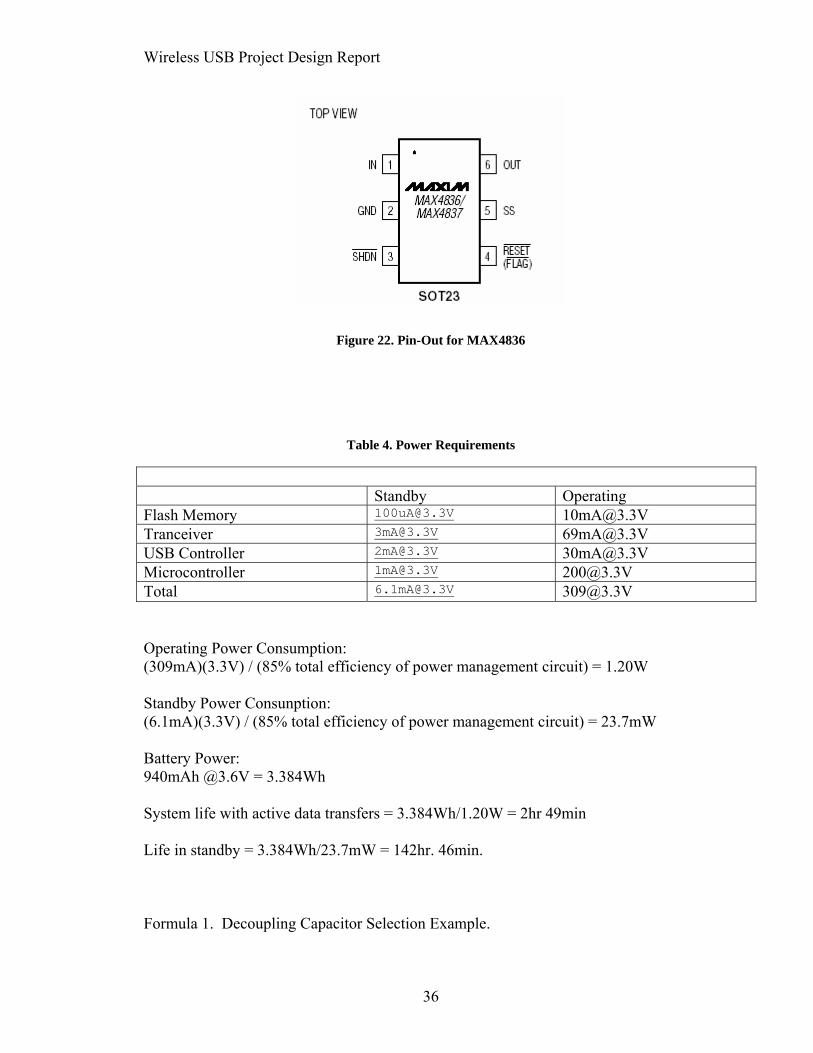
The Power Management circuit of the adapter module consists of a single 500 mA
MAX4836 LDO Regulator to convert the incoming 5V’s from the USB port to a preset-
at-order 3.3V to supply the USB controller, the transceiver, and the microcontroller. The
pin-out of the device is shown if figure 22. This circuit requires the adapter module to be
connected to a 500mA powered USB port.
Table 4 below shows the details of the estimated power required by the modules.
It was calculated that the adapter module should operate within the power supplied limits
of the USB port. It was calculated that the storage module will operate for nearly 3 hours
of data transfers, and over 142 hours in standby, more than long enough to make this a
practical device.
Both small decoupling capacitors and larger bypass capacitors are used for the
reliable operation of components throughout the entire circuit. In general capacitors
smooth out effects of AC transients on the DC supply voltages by supplying excess
charge when the voltage drops below the DC level and shunting off excess voltage
spikes. Decoupling capacitors are physically located as close to the input pin they are
filtering as possible, and connected between the particular voltage supply and ground. If
capacitor values are not specified by the manufacturer of the IC, decoupling capacitor
values are calculated using Formula 1 as given below with worst case conditions being
assumed.
34
Wireless USB Project Design Report
Figure 20. Pin-Out for MAX1874
Figure 21. Pin-Out for MAX8621
35
Wireless USB Project Design Report
Figure 22. Pin-Out for MAX4836
Table 4. Power Requirements
Standby Operating Flash Memory [email protected] [email protected] Tranceiver [email protected] [email protected] USB Controller [email protected] [email protected] Microcontroller [email protected] [email protected] Total [email protected] [email protected]
Operating Power Consumption: (309mA)(3.3V) / (85% total efficiency of power management circuit) = 1.20W Standby Power Consunption: (6.1mA)(3.3V) / (85% total efficiency of power management circuit) = 23.7mW Battery Power: 940mAh @3.6V = 3.384Wh System life with active data transfers = 3.384Wh/1.20W = 2hr 49min Life in standby = 3.384Wh/23.7mW = 142hr. 46min.
Formula 1. Decoupling Capacitor Selection Example.
36

Wireless USB Project Design Report
ICC(peak) = (60mA)*(I) Max ripple Voltage = (0.2Vpeak-peak)(0.1V dv) Switching time = 20ns dt C = I (dt/dv) C = (60mA*20ns) / 0.1V C = 12nF C = 12nF*(4x margin) = 0.047uF
Software Design:
A large majority of the implementation of this project will come in the form of
microcontroller software development. The embedded firmware code for the PIC
microcontroller will be written in C code. Because of the differences in the inherent
function between the adapter controller PIC and the controller chip dedicated for the flash
storage module side, there is a need for two separate bodies of code. To get an idea of
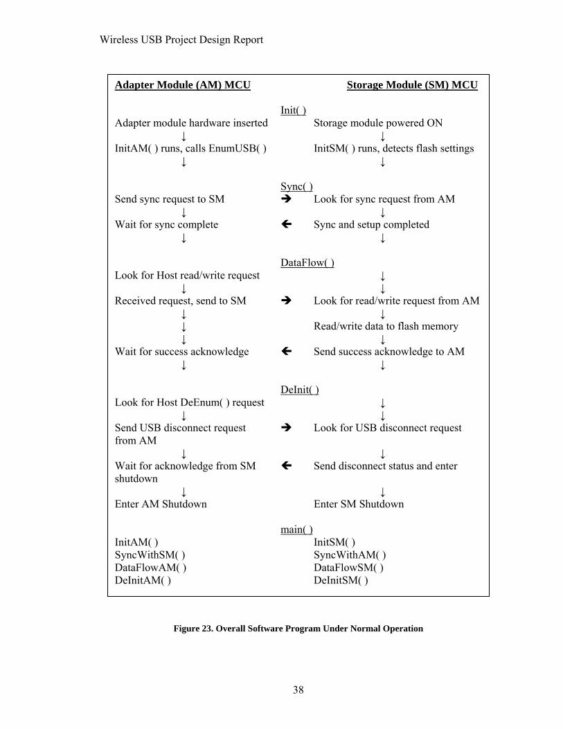
what the software flow under normal operation will look like, refer to the diagram below
labeled Figure 23.
37
Wireless USB Project Design Report
Adapter Module (AM) MCU Storage Module (SM) MCU Init( ) Adapter module hardware inserted Storage module powered ON ↓ ↓ InitAM( ) runs, calls EnumUSB( ) InitSM( ) runs, detects flash settings ↓ ↓ Sync( ) Send sync request to SM Look for sync request from AM ↓ ↓ Wait for sync complete Sync and setup completed ↓ ↓ DataFlow( ) Look for Host read/write request ↓ ↓ ↓ Received request, send to SM Look for read/write request from AM ↓ ↓ ↓ Read/write data to flash memory ↓ ↓ Wait for success acknowledge Send success acknowledge to AM ↓ ↓ DeInit( ) Look for Host DeEnum( ) request ↓ ↓ ↓ Send USB disconnect request Look for USB disconnect request from AM ↓ ↓ Wait for acknowledge from SM Send disconnect status and enter shutdown ↓ ↓ Enter AM Shutdown Enter SM Shutdown main( ) InitAM( ) InitSM( ) SyncWithSM( ) SyncWithAM( ) DataFlowAM( ) DataFlowSM( ) DeInitAM( ) DeInitSM( )
Figure 23. Overall Software Program Under Normal Operation
38
Wireless USB Project Design Report
This shows how the code on each of the two controllers run basically in parallel
until the synchronization between them occurs. First, and most importantly, the device
must answer configuration and descriptor requests from the host PC. This will require the
PIC on the adapter side to go through a series of host request and command transfers. The
USB host must assign a unique endpoint address to the device, it must determine the type
of device that it is (in this case it is classified as a mass storage device), it must determine
the data transfer types that will be used, and finally the speed at which it operates. These
are the most important of the many device descriptors that are sent to the host.
Once it has established its initial communication with the host, it must then
communicate with the PIC on the storage module side. Only after it receives information
about how much memory is available from the storage PIC, can the adapter finish its
USB host setup routine. The synchronization between the two PICs must then be
completed. The adapter PIC will then give the storage PIC the USB enumeration
acknowledgement and then the two modules are ready to exchange read/write data. Then
the program will enter an infinite loop which will look for read/write requests from the
host, check for de-initialization or disconnect requests from the host, and finally, check
for loss of connection by physical disconnect or by power failure on the storage side.
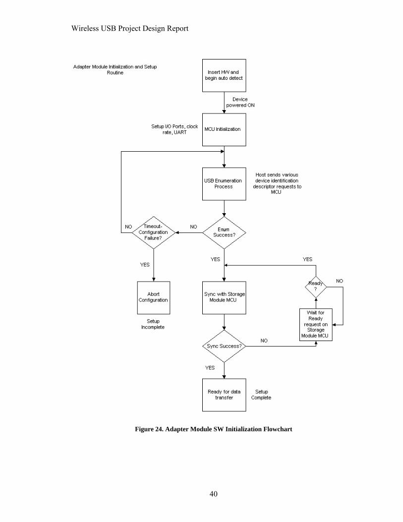
The most important part of the code is the setup and USB configuration, which is
required to correctly communicate with the USB host. The initial setup routine for the
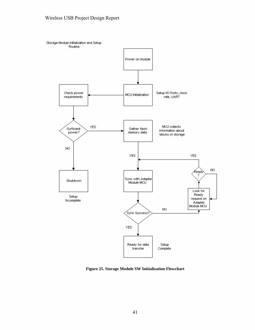
PIC controllers on each of the modules is listed below in flowchart form. Figure 24
shows the adapter module initialization flow diagram. Figure 25 shows the storage
module initialization flow diagram.
39
Wireless USB Project Design Report
Figure 24. Adapter Module SW Initialization Flowchart
40
Wireless USB Project Design Report
Figure 25. Storage Module SW Initialization Flowchart
41

Wireless USB Project Design Report
As you can see from the figures above, each must setup the MCU on power up. The
adapter controller then must begin to automatically begin handling device descriptor
requests form the USB Host. The storage controller will instead gather data about the
number of empty blocks of memory available for use within the flash device. Because the
storage module will undoubtedly be done with its tasks first, it will enter a short-term
wait state until the adapter controller sends a requests to gather information about the
flash to complete the host USB enumeration process. Of course, if the storage module has
to wait too long and does not have enough power, it will begin it soft shutdown routine.
Likewise, if the adapter controller fails during the enumeration requests and a certain
amount of retries pass, it will abort configuration and enter a failure state. However, as
long as these two attributes for each of the controllers are satisfied, each will continue to
send acknowledgement ping requests to each other until the wireless handshake between
the two modules is complete. In the main section of the controller code several tasks must
be completed.
The pseudo-code for the project is an important way to visualize the necessary
functions and program flow of the actual code that will be written during the
implementation of the project design. The overall pseudo-code for the design is provided
in the figures below. The two separate code blocks required for each controller are
similar but each is deserving of its own pseudo-code. Figure 26 gives the overall adapter
pseudo-code while Figure 27 provides the pseudo-code for the overall storage controller.
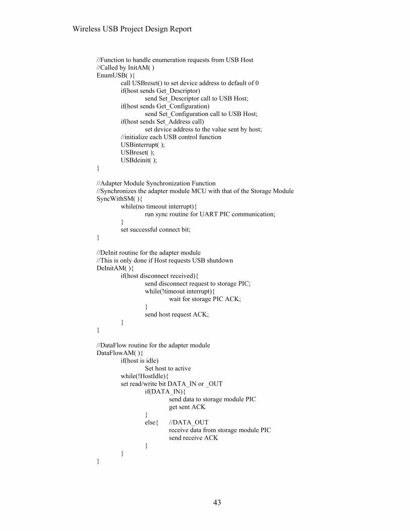
Adapter MCU Pseudo-code Functions: //Adapter Module Initialize Function InitAM( ){ Set Timer0 registers with appropriate prescaler; Configure ports A thru E and UART; }
42
Wireless USB Project Design Report
//Function to handle enumeration requests from USB Host //Called by InitAM( ) EnumUSB( ){
call USBreset() to set device address to default of 0 if(host sends Get_Descriptor) send Set_Descriptor call to USB Host; if(host sends Get_Configuration) send Set_Configuration call to USB Host; if(host sends Set_Address call) set device address to the value sent by host; //initialize each USB control function USBinterrupt( ); USBreset( ); USBdeinit( );
} //Adapter Module Synchronization Function //Synchronizes the adapter module MCU with that of the Storage Module SyncWithSM( ){
while(no timeout interrupt){ run sync routine for UART PIC communication; } set successful connect bit; } //DeInit routine for the adapter module //This is only done if Host requests USB shutdown DeInitAM( ){ if(host disconnect received){ send disconnect request to storage PIC; while(!timeout interrupt){ wait for storage PIC ACK; } send host request ACK; } } //DataFlow routine for the adapter module DataFlowAM( ){ if(host is idle) Set host to active
while(!HostIdle){ set read/write bit DATA_IN or _OUT if(DATA_IN){ send data to storage module PIC get sent ACK
} else{ //DATA_OUT receive data from storage module PIC send receive ACK }
} }
43
Wireless USB Project Design Report
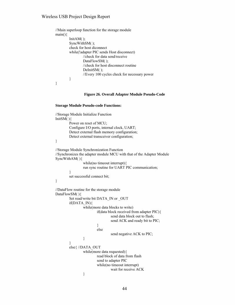
//Main superloop function for the storage module main(){ InitAM( ); SyncWithSM( ); check for host diconnect while(!adapter PIC sends Host disconnect) //check for data send/receive DataFlowSM( ); //check for host disconnect routine DeInitSM( ); //Every 100 cycles check for necessary power } }
Figure 26. Overall Adapter Module Pseudo-Code
Storage Module Pseudo-code Functions: //Storage Module Initialize Function InitSM( ){ Power on reset of MCU; Configure I/O ports, internal clock, UART; Detect external flash memory configuration; Detect external transceiver configuration; } //Storage Module Synchronization Function //Synchronizes the adapter module MCU with that of the Adapter Module SyncWithAM( ){
while(no timeout interrupt){ run sync routine for UART PIC communication; } set successful connect bit; } //DataFlow routine for the storage module DataFlowSM( ){ Set read/write bit DATA_IN or _OUT if(DATA_IN){ while(more data blocks to write)
if(data block received from adapter PIC){ send data block out to flash; send ACK and ready bit to PIC; } else send negative ACK to PIC; }
} else{ //DATA_OUT while(more data requested){ read block of data from flash send to adapter PIC while(no timeout interrupt) wait for receive ACK }
44
Wireless USB Project Design Report
} } //DeInit routine for the storage module //This is done for both USB Host shutdown and for hardware disconnect DeInitSM( ){ if(host disconnect message received from adapter PIC){ disconnect external memory I/O port; send ACK to adapter PIC; } } //Main superloop function for the storage module main( ){ InitSM( ); SyncWithAM( ); check for host diconnect while(!adapter PIC sends Host disconnect) //check for data send/receive DataFlowSM( ); //check for host disconnect routine DeInitSM( ); //Every 100 cycles check for necessary power } }
Figure 27. Overall Storage Module Pseudo-Code
The firmware code for each of the controllers will be tested using the PICDEM
development board from Microchip and the MPLAB development program in
conjunction with the MPLAB In-circuit debugger. These will be used to program and
debug the PIC microcontrollers.
Final Design Compromises:
The most important original goal that was ultimately unable to be achieved is the
feature of the 480-Mbits high-speed data rate of the USB 2.0 standard. The application
knowledge, testing requirements, and components needed to achieve this are not
available to an undergraduate non-profit design team and the final product using these
45

Wireless USB Project Design Report
data rates would be out of the financial scope of the project. This forced the design to
settle for the lower data transfer rates of the full-speed USB 2.0 specifications at
approximately 12Mbits per second. What’s more, the wireless transmission rates by
which the link between the two modules will communicate is further reduced in terms of
data rate capabilities. The CYWUSB6932 allows for a transmission rate of only
62.5kB/s. This is of course a big difference from the original goal of over 400MB/s,
however the lower data rates will not compromise the overall effectiveness and operation
of the project.
The other major compromise that was made is that the wireless communication
will not comply with the ultra-wideband (UWB) standard set forth by the WiMedia
Alliance as was originally intended. The Cypress wireless USB transceiver operates in
the 2.4GHz frequency range, much lower than what is required by the UWB standard.
Also, because a PIC microcontroller and a transceiver running at much lower data rates
were chosen, the project could not possible satisfy the requirements of the WiMedia
Alliance standard.
46
Wireless USB Project Design Report
Testing Procedures
Hardware Testing Procedures:
The first test that should be performed is testing the serial interface between the
storage module PIC and Toshiba NAND style, flash memory device. It should be verified
that the PIC is able to write blocks of data to the device as well as reading from the
device. Using a sequence of bit writes and reads, the flash storage device operation can
be confirmed.
The testing procedure for the wireless portion of the project will involve using a
separate controller other than the PIC to reduce the number of variables. The transceiver
will be powered up and then the registers will be set via the controller. Once the
transceiver has been properly powered up, both the transmission and reception will be
tested. The receiver and transmitter must be tested as a pair for the test to be completed.
The output of the receiver unit will be connected to the oscilloscope to monitor ensure
that the data is being received.
The testing procedure for the wired portion of the project will require correctly
interfacing the PIC controller and external wired USB transceiver to the PC through the
USB port. The code must correctly identify the device’s type and requirements during the
enumeration requests from the USB Host. Once it is confirmed that the USB host is able
to correctly identify and configure the device as a full-speed USB 2.0 mass storage
device, data can be transferred to the device to test the wired functionality.
Once the entire system is developed there will be two different tests that have to
be performed. One will be when the storage module is plugged directly into the USB port
via the male connector on the module. When this is plugged in, the PC should recognize
47

Wireless USB Project Design Report
the device as a mass storage device and then correctly build the drivers. When this is
complete the test will consist of transferring files from and to the device and making sure
that they can be read and written without error. The other test will be to connect the
adapter module to the USB port and then wirelessly transfer data from and to the storage
module.
As for the power management testing, all circuits will be constructed powered off
of bench top DC voltage supplies. Current readings will be made and verified to be
within the maximum ratings of the designed power management circuits. The power
management circuits will then be bread boarded and load tested to verify there output
voltages and current supply capabilities.
Software Testing Procedures:
Once the code for the controllers is written in C using the provided pseudo-code
skeleton provided in this report, the software testing and de-bugging process can begin.
The main goal will be to obtain a working solution. After the code is working, it will be
tweaked and improved for greater efficiency. Timing schemes will be slower than desired
at first so as to ensure a working solution. Later, the timing should be cut down so that
the device runs at optimal performance levels.
Another test that will most likely be applied to the code is the possibility of using
a real-time operating system approach instead of the provided “superloop” function. This
test would weigh the positives and negatives of using this approach to determine whether
it would be worth the extra development time required to implement it. One obvious
benefit would be that it would allow the system to perform multiple tasks at the same
48

Wireless USB Project Design Report
time making it closer in operation to its PC counterpart. The standard “superloop”
technique will work, however, and is the safe route to a working project.
49

Wireless USB Project Design Report
Financial Budget
The project was granted a departmental budget which was not to exceed $100 per
person for use towards parts needed. The project for material parts did not exceed $300,
hence external funding was not required. Any products listed as a cost of $0.00 denotes
that it was acquired or borrowed from the department. All listed costs are estimates. The
labor costs are simply included to estimate typical labor costs associated with what a
‘real’ project budget might look like.
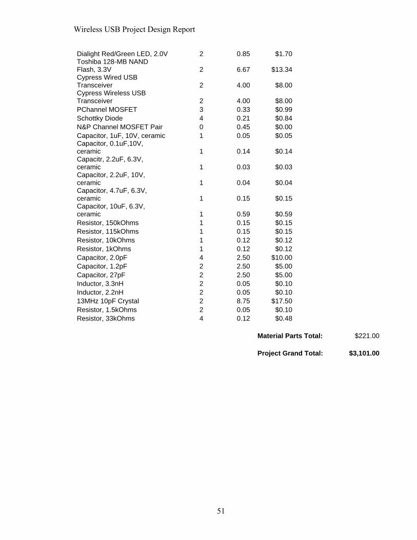
Table 5. Project Budget Sheet
Labor Costs: Cost per person per hour (USD): $10.00
Design Team Member Weeks Hours/Week Cost/Week Est. Total Cost
Czapor, Jeff 12 8 $80.00 $960.00Hartney, Ben 12 8 $80.00 $960.00Knight, Andrew 12 8 $80.00 $960.00 Total: $2,880.00 Material Costs: Estimated costs & quantities of suggested parts. Material Part Description Quantity Cost/Item Part Total PIC18F4550 Microcontroller 40-Pin PDIP 2 $9.41 $18.82 PIC18LF4550 Low Power 40-Pin PDIP 2 $11.00 $22.00 PIC18F4550 Development Board 1 59.99 $59.99 MPLAB Software Development Program 1 0.00 $0.00 MPLAB In-Circuit Debugger 1 0.00 $0.00 Maxim/Dallas Semiconductor Battery Charger 1 3.54 $3.54 Maxim/Dallas Semiconductor DC/DC Converters 2 7.71 $15.42 ASSMANN Male USB Plug 1 0.92 $0.92 Female USB Plug 1 7.67 $7.67 Panasonic Li-Ion Battery, 3.6V 1 19.95 $19.95
50
Wireless USB Project Design Report
Dialight Red/Green LED, 2.0V 2 0.85 $1.70 Toshiba 128-MB NAND Flash, 3.3V 2 6.67 $13.34 Cypress Wired USB Transceiver 2 4.00 $8.00 Cypress Wireless USB Transceiver 2 4.00 $8.00 PChannel MOSFET 3 0.33 $0.99 Schottky Diode 4 0.21 $0.84 N&P Channel MOSFET Pair 0 0.45 $0.00 Capacitor, 1uF, 10V, ceramic 1 0.05 $0.05 Capacitor, 0.1uF,10V, ceramic 1 0.14 $0.14 Capacitr, 2.2uF, 6.3V, ceramic 1 0.03 $0.03 Capacitor, 2.2uF, 10V, ceramic 1 0.04 $0.04 Capacitor, 4.7uF, 6.3V, ceramic 1 0.15 $0.15 Capacitor, 10uF, 6.3V, ceramic 1 0.59 $0.59 Resistor, 150kOhms 1 0.15 $0.15 Resistor, 115kOhms 1 0.15 $0.15 Resistor, 10kOhms 1 0.12 $0.12 Resistor, 1kOhms 1 0.12 $0.12 Capacitor, 2.0pF 4 2.50 $10.00 Capacitor, 1.2pF 2 2.50 $5.00 Capacitor, 27pF 2 2.50 $5.00 Inductor, 3.3nH 2 0.05 $0.10 Inductor, 2.2nH 2 0.05 $0.10 13MHz 10pF Crystal 2 8.75 $17.50 Resistor, 1.5kOhms 2 0.05 $0.10 Resistor, 33kOhms 4 0.12 $0.48 Material Parts Total: $221.00 Project Grand Total: $3,101.00
51
Wireless USB Project Design Report
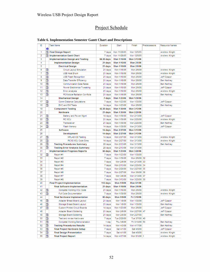
Project Schedule
Table 6. Implementation Semester Gantt Chart and Descriptions
52
Wireless USB Project Design Report
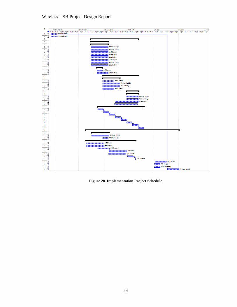
Figure 28. Implementation Project Schedule
53

Wireless USB Project Design Report
Design Team Information
Team Members:
Jeff Czapor - Electrical Engineering Student
Ben Hartney - Electrical Engineering Student
Andrew Knight - Computer Engineering Student
Faculty Advisor:
Dr. Ugweje - Department of Electrical and Computer Engineering
54

Wireless USB Project Design Report
Conclusions and Recommendations
This project is ready for the full implementation stage. Though the design has
been scaled down in performance considerably from its original form, it can still prove to
be an efficient and reliable mass storage device peripheral application. It will be easily
configurable and universally accepted as any USB flash device. It will demonstrate the
wireless feature within a generous distance from the PC to which it connects. Data rates
for the project are going to be much lower than what was initially intended, however it
will still get the job done. The wireless communication protocol will not satisfy the
originally anticipated goal of working within the specifications of the WiMedia Alliance
ultra-wideband standards, but it can display a reliable wireless connection in the widely
used 2.4GHz frequency range.
As a warning to anyone who is seeking to use the new Wireless USB standard in a
similar project design, the technology needs to mature a little more before it will be as
universally tested and implemented as its wired counterpart. What seemed to be merely
an ambitious project turned out to needing up-to-the-minute technology which was
simply out of the scope of a senior design project. By lowering the performance
requirements of this project, it will be a working success. It will satisfy the goals and
design specifications that we set in terms of functionality, reliability, and interoperability.
By focusing on the necessities of the project, the implementation should be a satisfying
reward for all the setbacks and difficulties of the design process.
55
Wireless USB Project Design Report
References
1. Axelson, Jan. USB Complete, Second Edition. Lakeview Research c. 2001
2. Cypress Wireless USB LS 2.4-GHz DSSS Radio SoC Datasheet. Cypress
Semiconductor Corporation c. 2005.
3. Dipert, Brian & Levy, Marcus. Designing with Flash Memory. Anabooks c. 1994.
4. Dual Step-Down DC-DC Power Management IC MAX8621YETG. Maxim
Integrated Products.
5. Flash Memory TC58128AFT Data Sheet. Toshiba c. 2001.
6. Li+ Charger IC MAX1874ETE Data Sheet. Maxim Integrated Products.
7. Microchip PIC18F4550 Data Sheet. Microchip Technology Inc c. 2004.
8. Wireless Universal Serial Bus Specification, Revision 1.0. USB Implementers
Forum c. 2005.
9. 500mA LDO Data Sheet. Maxim Integrated Products.
56


