Embed Size (px)
Citation preview
Università degli Studi di Catania
Dottorato di Ricerca Internazionale in Ingegneria dei Sistemi
XXVI Ciclo
Gaetano L’Episcopo
Nonlinear Methodologies in Transduction
Mechanisms for Energy Harvesting and Sensors
Ph.D. Thesis
Coordinator: Prof. Ing. Luigi Fortuna
Tutor: Prof. Ing. Salvatore Baglio
2013

To those who believed in me
Abstract
The constant need of improving performance of trans-
ducers has pushed scientists to searching novel solutions in
transduction mechanisms. The development of theories about
Stochastic Resonance and the interplay between nonlinearity
and noise represents one of the proposed strategies to improve
performance of actual transducers in certain operating condi-
tions.
Among nonlinear systems, bistable mechanisms have been
investigated in this work. Several results of their application
in the field of energy harvesting from mechanical vibrations
and in the sensing of AC currents are presented with a special
focus on the benefits due to their adoption in specific applica-

Abstract
tions where traditional approaches based on linear transduc-
tion mechanisms exhibit issues in efficiency.
A special attention is also paid to the technological solu-
tions to implement prototypes of integrated bistable devices
and several rapid prototyping strategies are investigated and
proposed.
IV
Contents
Introduction . . . . . . . . . . . . . . . . . . . . . . . . . . . . . . . . . . . . 1
Linear and nonlinear strategies in transduction
mechanisms . . . . . . . . . . . . . . . . . . . . . . . . . . . . . . . . . 5
1.1 Linear and nonlinear transduction strategies . . . 5
1.2 Nonlinear transduction methodologies: bistable
strategies . . . . . . . . . . . . . . . . . . . . . . . . . . . . . . . . . 12
1.3 Applications of bistable strategies: energy
harvesting and sensors . . . . . . . . . . . . . . . . . . . . . . 21
1.3.1 Applications of bistable mechanisms in
sensors . . . . . . . . . . . . . . . . . . . . . . . . . . . . . . 22
1.3.2 Application of bistable mechanisms in
energy harvesting from vibrations . . . . . . . 34
Contents
Technologies to fabricate integrated bistable
devices . . . . . . . . . . . . . . . . . . . . . . . . . . . . . . . . . . . . . . 41
2.1 Microelectromechanical Systems (MEMS) . . . . . 42
2.1.1 CNM BESOI process . . . . . . . . . . . . . . . . . . 46
2.1.2 MEMSCAP MetalMUMPs® process . . . . 52
2.1.3 MEMSCAP PiezoMUMPs® process . . . . . 56
2.1.4 STMicroelectronics ThELMA® process . . 60
2.1.5 Radiant pMEMs® process . . . . . . . . . . . . . 64
2.2 Rapid prototyping of devices in Nanotechnology 68
2.2.1 FIB milling of nano-cantilever beams . . . . 72
2.2.2 Deposition of Zinc Oxide through Pulsed
Plasma Deposition . . . . . . . . . . . . . . . . . . . . 86
2.3 Devices in direct printing technology . . . . . . . . . 100
Bistable devices for vibration energy harvesting . 113
3.1 Energy harvesting from vibrations: state of the
art . . . . . . . . . . . . . . . . . . . . . . . . . . . . . . . . . . . . . . . 114
3.1.1 Sources of energy . . . . . . . . . . . . . . . . . . . . . 118
3.1.2 Sources of mechanical vibrations . . . . . . . . 121
3.1.3 Architecture of vibration energy harvesters128
3.1.4 Linear resonant coupling structures . . . . . 131
VI
Contents
3.1.5 Coupling mechanical structures: from
linear to nonlinear . . . . . . . . . . . . . . . . . . . . 137
3.1.6 Nonlinear coupling structures . . . . . . . . . . . 144
3.1.7 Mechanical-to-electrical transduction
strategies . . . . . . . . . . . . . . . . . . . . . . . . . . . . 155
3.2 Bistable MEMS devices for vibration energy
harvesting in the CNM BESOI process . . . . . . . . 185
3.2.1 Device modeling . . . . . . . . . . . . . . . . . . . . . . 187
3.2.2 Numerical analyses and results . . . . . . . . . 197
3.2.3 Design of the vibration MEMS energy
harvester . . . . . . . . . . . . . . . . . . . . . . . . . . . . 204
3.2.4 Considerations on mechanical-to-
electrical energy conversion . . . . . . . . . . . . . 218
3.3 Bistable MEMS devices for vibration
energy harvesting in the STMicroelectronics
ThELMA® process . . . . . . . . . . . . . . . . . . . . . . . . 228
3.3.1 The mechanical microstructure . . . . . . . . . 229
3.3.2 FEM analyses of the microstructure . . . . . 229
3.3.3 Considerations on mechanical-to-
electrical transduction . . . . . . . . . . . . . . . . . 234
VII
Contents
3.4 Bistable microstructure in the
MEMSCAP MetalMUMPs® process . . . . . . . . . . 243
3.4.1 Cascaded triple bent-beam structure . . . . 243
3.4.2 FEM simulations . . . . . . . . . . . . . . . . . . . . . 244
3.4.3 Test of the microstructure . . . . . . . . . . . . . 247
3.5 Bistable devices for vibration energy harvesting
in in direct printing technology . . . . . . . . . . . . . . 251
3.5.1 The device and its working principle . . . . . 255
3.5.2 Design flow . . . . . . . . . . . . . . . . . . . . . . . . . . 259
3.5.3 Mechanical Characterization . . . . . . . . . . . 261
3.5.4 Electrical Characterization . . . . . . . . . . . . . 266
Bistable devices for AC current sensors . . . . . . . . . 275
4.1 State of art for AC current sensors . . . . . . . . . . . 276
4.1.1 Techniques for current sensing . . . . . . . . . . 277
4.1.2 MEMS AC current sensors . . . . . . . . . . . . . 283
4.2 Bistable AC current sensor . . . . . . . . . . . . . . . . . . 287
4.3 Bistable AC current sensor modeling . . . . . . . . . 292
4.4 Bistable AC current microsensor in
PiezoMUMPs® process . . . . . . . . . . . . . . . . . . . . . 302
4.4.1 Device simulations . . . . . . . . . . . . . . . . . . . . 307
VIII
Contents
4.5 Macroscale prototype of the bistable AC
current sensor . . . . . . . . . . . . . . . . . . . . . . . . . . . . . 350
4.5.1 Prototype characteristics and
measurement setup . . . . . . . . . . . . . . . . . . . 351
4.5.2 Measurement results . . . . . . . . . . . . . . . . . . 355
Conclusions . . . . . . . . . . . . . . . . . . . . . . . . . . . . . . . . . . . . . 369
Acknowledgements . . . . . . . . . . . . . . . . . . . . . . . . . . . . . . 373
Activities during Ph.D. course . . . . . . . . . . . . . . . . . 377
A.1 Publications on international journals . . . . . . . . . 377
A.2 International conference proceedings . . . . . . . . . . 378
A.3 Book contributions . . . . . . . . . . . . . . . . . . . . . . . . . 379
A.4 Publications on Italian journals . . . . . . . . . . . . . . 380
A.5 Italian conference proceedings . . . . . . . . . . . . . . . 380
A.6 Attended conferences . . . . . . . . . . . . . . . . . . . . . . . 382
A.7 Attended Ph.D. schools . . . . . . . . . . . . . . . . . . . . . 382
A.8 Attended contests . . . . . . . . . . . . . . . . . . . . . . . . . . 382
A.9 Attended courses at the University of Catania
(Italy) . . . . . . . . . . . . . . . . . . . . . . . . . . . . . . . . . . . . 383
IX
Contents
A.10 Tutoring Activities at University of Catania
(Italy) . . . . . . . . . . . . . . . . . . . . . . . . . . . . . . . . . . . . 383
References . . . . . . . . . . . . . . . . . . . . . . . . . . . . . . . . . . . . . . 385
General References . . . . . . . . . . . . . . . . . . . . . . . . . . . . . 391
Nonlinearity and Stochastic Resonance . . . . . . . . . . . 397
Bistable Systems . . . . . . . . . . . . . . . . . . . . . . . . . . . . . . 403
Technology References . . . . . . . . . . . . . . . . . . . . . . . . . . 414
Energy Harvesting . . . . . . . . . . . . . . . . . . . . . . . . . . . . . 434
Electric Current Sensors . . . . . . . . . . . . . . . . . . . . . . . . 441
Internet Links . . . . . . . . . . . . . . . . . . . . . . . . . . . . . . . . . 443
List of Figures . . . . . . . . . . . . . . . . . . . . . . . . . . . . . . . . . . 444
List of Tables . . . . . . . . . . . . . . . . . . . . . . . . . . . . . . . . . . . 488
X
Introduction
Stay foolish. Stay hungry.
Steve Jobs
The constant need to improve performance and the al-
ways widening range of applications for electronic-based de-
vices push scientific research toward the endless exploration
for novel solutions that can advance the state of the art over-
coming traditional approaches.
Among electronics devices, a special attention is reserved
to transducers (i.e. systems able to convert signals in one form
of energy to another form) for their wide range of applications
in sensing, actuating and energy harvesting.
Introduction
Very often, transducers are considered to exploit linear
mechanisms thus, the output signal or power is almost lin-
early proportional to the input in this case. However, although
to consider a linear working principle helps to reduces the
complexity of system handling and implementation, some is-
sues in performance have been revealed when linear strategies
are adopted in applications involving nonlinearities and noise.
As shown in this work, for example, sensitivity in sensors is
strongly affected by noise and linear energy harvesters from
mechanical vibrations exhibit poor performance when wide-
band noisy vibrations are addressed as source energy to be
scavenged. Therefore linear approaches, even if generally sim-
pler, are not alway optimal and often the efforts descending
from taking into account a more complex model rewards with
better overall perfomances.
Some solutions exploiting nonlinear transducers and the
interplay between noise and nonlinear dynamics have been
proposed in literature, especially after the development of the
theories about Stochastic Resonance, and have been shown to
represent an effective way to overcome traditional limitations
2
Introduction
of linear transducers and therefore to improve their perfor-
mances.
In this work, nonlinear transduction mechanisms will be
presented with a special focus on bistable strategies with sev-
eral applications in the sensors field and in the energy harvest-
ing from mechanical vibrations. Efforts will be paid to show
the technical feasibility of the proposed solutions and to prove
the performance improvement descending from nonlinearities.
In the first chapter, motivations of the adoption of nonlin-
ear strategies in transduction mechanisms will be discussed
by supporting them with theory and comparisons with linear
transducers. Among nonlinear mechanisms, the attention will
be focused on bistable strategies and the state of the art of
their application in the field of sensors and of energy harvest-
ing will be presented.
In the second chapter, several technology solutions to im-
plement bistable devices will be treated. First of all, suitable
standard technology processes to develop microscale devices
in the field of microelectromechanical systems (MEMS) will
be presented; secondly, some useful strategies and some re-
3

Introduction
sults for rapid prototyping in Nanotechnology will be pre-
sented and, finally, an approach for rapid prototyping of low
cost devices of centimeter size exploiting direct printing tech-
nology will be proposed.
In the third chapter, after covering the state of the art
in the energy harvesting from mechanical vibrations, some
solutions exploiting mechanically bistable oscillators will be
proposed both in the field of MEMS and in direct printing
technology. Models simulations along with experimental re-
sults will be presented to prove the feasibility of the proposed
devices.
In the fourth chapter, attention will be focused on bistable
AC current sensors and, after discussing the state of the art
in this field, a bistable sensor for AC currents capable of scav-
enging energy from its own operative environment will be pro-
posed along with its behavioral model and an experimental
device prototype for testing.
4
1
Linear and nonlinear strategies in
transduction mechanisms
Science shines forth in all its value as a good capable of motivating our
existence, as a great experience of freedom for truth, as a fundamental work
of service. Through research each scientist grows as a human being and helps
others to do likewise.
John Paul II
1.1 Linear and nonlinear transduction
strategies
There are many aspects of the environment that people
need and/or want to monitor or modify for a wide range of
purposes. Some examples of physical and chemical quantities
1.1. LINEAR AND NONLINEAR TRANSDUCTION STRATEGIES
of interest are given by temperature, light intensity, mechan-
ical vibrations, air pressure, humidity, chemicals present in
water, chemical pollutants in air and so on. In order to handle
such quantities, devices able to convert and relate with dif-
ferent physical and chemical fields are requested. Transducers
represent this sort of specially made devices to respond to a
chosen energy source and transform it into a different form
of energy through a defined transduction mechanism. Trans-
ducers can be divided into sensors and actuators; sensors are
used to detect a parameter in one form and report it in an-
other form of energy, often an electrical signal, while actuators
accepts energy as input and produces an action (e.g., move-
ment) [249].
The traditional approach in implementing transduction
mechanisms has been based on linear strategies. In these cases,
the device transduction function is represented by a linear
mathematical function (i.e. a straight line in a graph) ex-
pressing a linear proportional relationship between the input
and the output quantities. As an example, this means that
to a given variation of the sensed quantity corresponds a pro-
6
CHAPTER 1. LINEAR AND NONLINEAR STRATEGIES IN TRANSDUCTIONMECHANISMS
portional variation in the output signal of sensors. Deviations
from such linear behaviour have been characterized in the
specifications of transducers in terms of nonlinearity errors
(e.g., the deviation of the device from its nominal linear oper-
ation) because nonlinearity has been traditionally considered
as a negative point in transducers [70].
Since the beginnings of modern engineering sciences, the
use of linear systems has been preferred by engineers and
physicists to nonlinear systems because linear transducers sat-
isfy mathematical properties like proportionality, superposi-
tion and homogeneity, which can greatly simplify their model-
ing, design and control in terms of analytical efforts and com-
putational and development costs. In addition, linear time-
invariant systems with zero initial conditions and zero-point
equilibrium (i.e. a subset of linear systems) take advantage of
transfer functions as useful mathematical representations of
the input-output relationship, in terms of spatial or temporal
frequency [84].
Although linear strategies are simpler to handle, nature is
intrinsically highly nonlinear. Due to the complex interaction
7
1.1. LINEAR AND NONLINEAR TRANSDUCTION STRATEGIES
among physical and chemical fields, the nonlinear behaviour
can be certainly recognized as the ordinary feature of the vast
majority of physical and chemical systems [227]. Sometimes,
in engineering sciences, linear features of systems come from
approximations of nonlinear behaviours. In the case of sen-
sors, as an example, the linear behaviour is often exhibited
only in a small interval of values of their operative range or
under specific restricted conditions, thus limiting the sensor
application range [177].
Recent studies about transducers have revealed some bene-
fits of nonlinear transduction strategies over linear approaches,
under certain conditions in some applications such as sensors
and energy harvesting [92].
It is known that noise (intended both as any spurious dis-
turb that superimposes and/or distorts the original signal pro-
duced by the transducer and as fluctuations affecting the rel-
evant parameters of the transducer) is one of hardest unpleas-
ant aspect in any linear transducer design. In fact, noise can
significantly affect linear transducers performance by limit-
ing their sensitivity and their dynamic range and increasing
8
CHAPTER 1. LINEAR AND NONLINEAR STRATEGIES IN TRANSDUCTIONMECHANISMS
signal distortion and leading them to exhibit an unwanted
“nonlinear” behaviour [105].
On the contrary, many scientists have recently started to
take a novel approach in transducers studies where noise and
nonlinearity play a key role in the operation of some physical
and chemical nonlinear systems. The most famous example of
the work developed in this direction is probably due to the dis-
covery of the stochastic resonance phenomenon [40, 91] where
a proper quantity of noise can make a periodically driven bi-
stable dynamic system to switch in synchrony with its driving
input. As an example of the exploitation of stochastic reso-
nance, a signal that is normally too weak to be detected by
a sensor can be boosted by adding white noise to the signal,
which contains a wide spectrum of frequencies; the frequen-
cies in the white noise corresponding to the original frequen-
cies of the signal will resonate with each other, amplifying
the original signal while not amplifying the rest of the white
noise (thereby increasing the signal-to-noise ratio which makes
the original signal more prominent). Furthermore, the added
white noise can be enough to be detectable by the sensor,
9
1.1. LINEAR AND NONLINEAR TRANSDUCTION STRATEGIES
which can then filter it out to effectively detect the original,
previously-undetectable signal [89].
Initially proposed as a possible explanation of the periodic
recurrence of Earth ice ages [29], stochastic resonance has be-
come a general paradigm for periodically driven noisy nonlin-
ear dynamical systems [2]. Following the pioneering works on
stochastic resonance, other studies have been developed in or-
der to exploit the potential benefits of the interplay between
noise and nonlinearities [104]. In the above mentioned field
of sensors, a novel class of “noise activated nonlinear devices”
has been introduced. In these devices noise and nonlinear re-
sponse can be exploited in the framework of a different mea-
surement strategy that allows for improving devices sensitiv-
ity and simplifying readout schemes [88]. This new approach
is based on the monitoring of the mean residence time dif-
ference. The residence time is the time spent by the system
output in each of its stable equilibrium states. The switches
among these stable equilibrium states are affected both by
the unknown target signal and the noise present during mea-
surements [67]. A careful consideration of the statistics in the
10
CHAPTER 1. LINEAR AND NONLINEAR STRATEGIES IN TRANSDUCTIONMECHANISMS
residence time can lead to extract useful information about
the hidden target signal [42]. This nonlinear transduction ap-
proach has been effectively exploited in the development of
residence-times fluxgate magnetometers [14, 41] and electric
field sensors based on ferroelectric materials [12, 13].
Another example of the benefits of nonlinear transducers
in noisy environments is represented by the exploitation of
the properties of non-resonant oscillators, characterized by a
nonlinear dynamic response, in the harvesting of energy from
mechanical vibrations [60, 92]. In fact, it has been demon-
strated that, in presence of mechanical vibrations having wide
spectrum at low frequencies (e.g., below 500 Hz), thus resem-
bling a band-limited white noise, the application of nonlinear
transducers can allow for scavenging a larger amount of energy
than linear transducers thanks to their wider bandwidth [83,
235].
11
1.2. NONLINEAR TRANSDUCTION METHODOLOGIES: BISTABLESTRATEGIES
1.2 Nonlinear transduction methodologies:
bistable strategies
Among nonlinear systems, since last decades bistable sys-
tems have been playing a prominent role in the field of nonlin-
ear transducers exploiting benefits from stochastic resonance
and noise [90, 167].
In its mathematical formulation, a system is defined “bi-
stable” when it exhibits two stable equilibrium states, accord-
ing to Lyapunov’s theory [148], and one unstable equilibrium
state between the two aforesaid stable equilibrium states. This
formulation means that, if a bistable system lies in one of its
stable equilibrium states, even if it is subjected to a “small
perturbation” from an external forcing, the system will con-
tinue to keep its stable equilibrium state and/or, at least, it
will continue to oscillate around it as long as the perturbation
is smaller than a “certain limit value”. When the applied en-
ergy of the incoming perturbation is large enough to overcome
a defined barrier (i.e. the unstable equilibrium state) between
the two stable equilibrium states, the system will switch to
the other stable equilibrium state. At this point, that stable
12
CHAPTER 1. LINEAR AND NONLINEAR STRATEGIES IN TRANSDUCTIONMECHANISMS
equilibrium state will tend to be maintained until another ex-
ternal forcing, larger than a defined level, will lead the system
to the previous stable equilibrium state. The behaviour of a
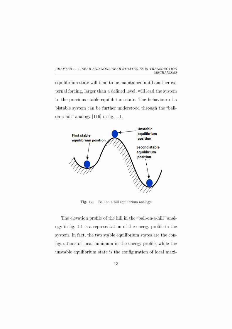
bistable system can be further understood through the “ball-
on-a-hill” analogy [116] in fig. 1.1.
Fig. 1.1 – Ball on a hill equilibrium analogy.
The elevation profile of the hill in the “ball-on-a-hill” anal-
ogy in fig. 1.1 is a representation of the energy profile in the
system. In fact, the two stable equilibrium states are the con-
figurations of local minimum in the energy profile, while the
unstable equilibrium state is the configuration of local maxi-
13
1.2. NONLINEAR TRANSDUCTION METHODOLOGIES: BISTABLESTRATEGIES
mum. Since dynamical systems attempt to remain in the low-
est energy state possible, according to the Lagrange-Dirichlet
theorem [38], no external energy is needed to maintain the sys-
tem in its stable equilibrium states. However, due to different
energetic levels between each of the two stable equilibrium
states and the unstable equilibrium state (which defines the
“energy barrier” of the system), external energy must be sup-
plied to allow for commutations between the two stable equi-
librium states in order to firstly come up the adverse energy
slope, secondly to overtake the unstable equilibrium state and
lastly to reach to the other stable equilibrium state by tak-
ing advantage of the favourable energy slope after passing the
unstable equilibrium state (see fig. 1.1). The amount of exter-
nal energy required to snap from the first stable equilibrium
state to the second one could be different from the quantity
of energy needed to switch in the opposite direction because
of the eventual asymmetry in the energy level of the stable
equilibrium states. In the case of asymmetry, there is a higher
probability that the system will spend more time in its stable
equilibrium state having the lower energy level [171].
14
CHAPTER 1. LINEAR AND NONLINEAR STRATEGIES IN TRANSDUCTIONMECHANISMS
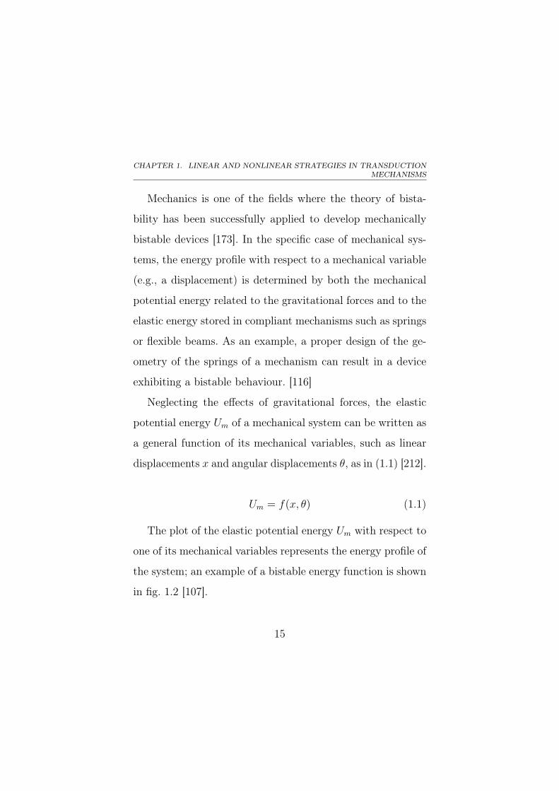
Mechanics is one of the fields where the theory of bista-
bility has been successfully applied to develop mechanically
bistable devices [173]. In the specific case of mechanical sys-
tems, the energy profile with respect to a mechanical variable
(e.g., a displacement) is determined by both the mechanical
potential energy related to the gravitational forces and to the
elastic energy stored in compliant mechanisms such as springs
or flexible beams. As an example, a proper design of the ge-
ometry of the springs of a mechanism can result in a device
exhibiting a bistable behaviour. [116]
Neglecting the effects of gravitational forces, the elastic
potential energy Um of a mechanical system can be written as
a general function of its mechanical variables, such as linear
displacements x and angular displacements θ, as in (1.1) [212].
Um = f(x, θ) (1.1)
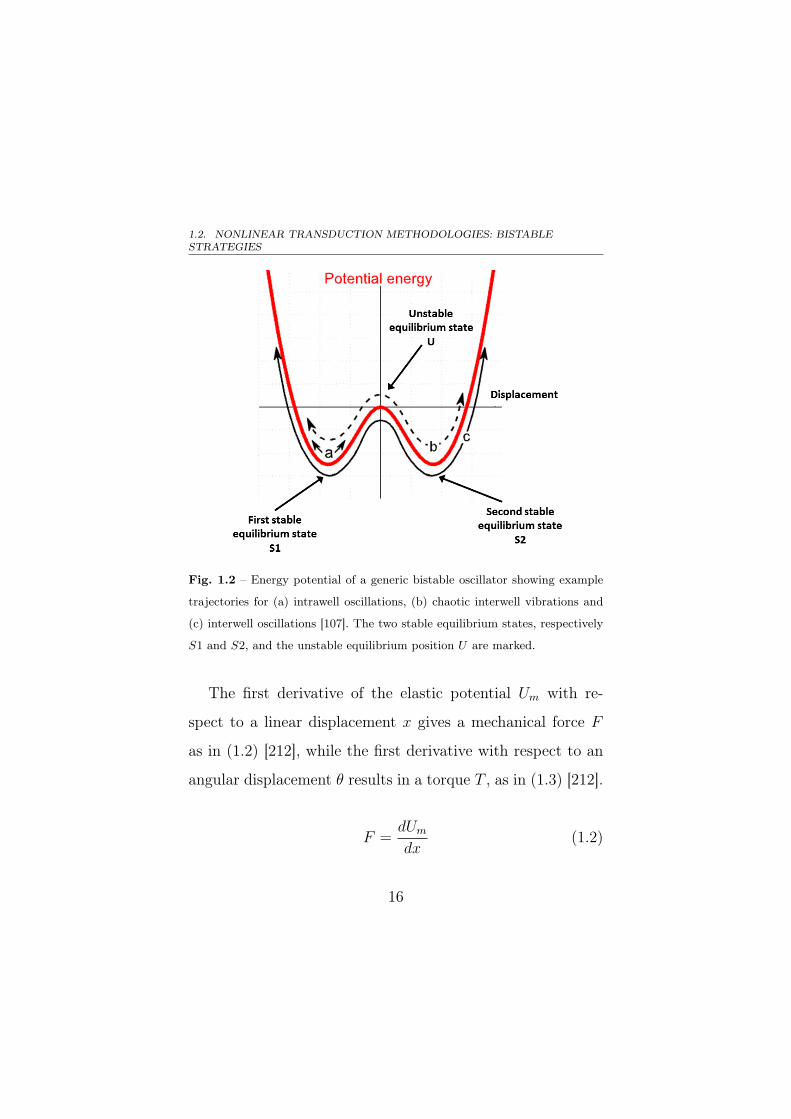
The plot of the elastic potential energy Um with respect to
one of its mechanical variables represents the energy profile of
the system; an example of a bistable energy function is shown
in fig. 1.2 [107].
15
1.2. NONLINEAR TRANSDUCTION METHODOLOGIES: BISTABLESTRATEGIES
Fig. 1.2 – Energy potential of a generic bistable oscillator showing example
trajectories for (a) intrawell oscillations, (b) chaotic interwell vibrations and
(c) interwell oscillations [107]. The two stable equilibrium states, respectively
S1 and S2, and the unstable equilibrium position U are marked.
The first derivative of the elastic potential Um with re-
spect to a linear displacement x gives a mechanical force F
as in (1.2) [212], while the first derivative with respect to an
angular displacement θ results in a torque T , as in (1.3) [212].
F =dUmdx
(1.2)
16
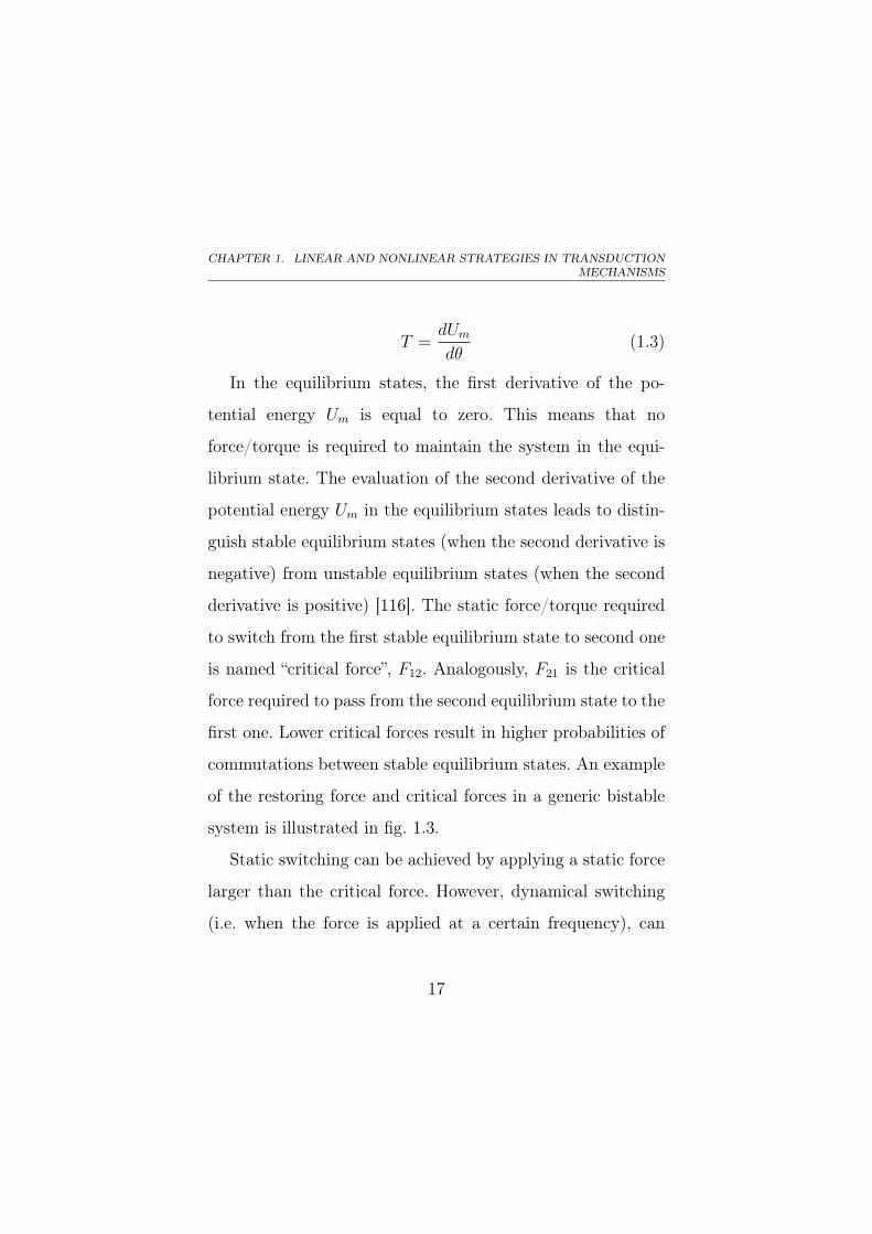
CHAPTER 1. LINEAR AND NONLINEAR STRATEGIES IN TRANSDUCTIONMECHANISMS
T =dUmdθ
(1.3)
In the equilibrium states, the first derivative of the po-
tential energy Um is equal to zero. This means that no
force/torque is required to maintain the system in the equi-
librium state. The evaluation of the second derivative of the
potential energy Um in the equilibrium states leads to distin-
guish stable equilibrium states (when the second derivative is
negative) from unstable equilibrium states (when the second
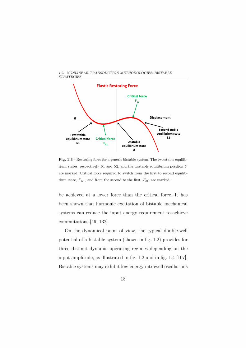
derivative is positive) [116]. The static force/torque required
to switch from the first stable equilibrium state to second one
is named “critical force”, F12. Analogously, F21 is the critical
force required to pass from the second equilibrium state to the
first one. Lower critical forces result in higher probabilities of
commutations between stable equilibrium states. An example
of the restoring force and critical forces in a generic bistable
system is illustrated in fig. 1.3.
Static switching can be achieved by applying a static force
larger than the critical force. However, dynamical switching
(i.e. when the force is applied at a certain frequency), can
17
1.2. NONLINEAR TRANSDUCTION METHODOLOGIES: BISTABLESTRATEGIES
Fig. 1.3 – Restoring force for a generic bistable system. The two stable equilib-
rium states, respectively S1 and S2, and the unstable equilibrium position U
are marked. Critical force required to switch from the first to second equilib-
rium state, F12 , and from the second to the first, F21, are marked.
be achieved at a lower force than the critical force. It has
been shown that harmonic excitation of bistable mechanical
systems can reduce the input energy requirement to achieve
commutations [46, 132].
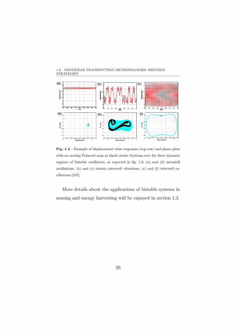
On the dynamical point of view, the typical double-well
potential of a bistable system (shown in fig. 1.2) provides for
three distinct dynamic operating regimes depending on the
input amplitude, as illustrated in fig. 1.2 and in fig. 1.4 [107].
Bistable systems may exhibit low-energy intrawell oscillations
18
CHAPTER 1. LINEAR AND NONLINEAR STRATEGIES IN TRANSDUCTIONMECHANISMS
as in figure 1(a). In this case, the system oscillates around one
of the two stable equilibrium states with a small stroke per
forcing period as in fig. 1.4(a) and phase portrait with an over-
lay Poincaré map as in fig. 1.4(d). Alternatively, the bistable
oscillator may be excited to a degree so as to exhibit aperiodic
or chaotic vibrations between stable equilibrium states such as
in fig. 1.4(b) and fig. 1.4(e). As the excitation amplitude is in-
creased still further, the device may exhibit periodic interwell
oscillations (also known as high energy orbits or snap-through
behaviour) as in fig. 1.4(c) and fig. 1.4(f). In some cases, the
dynamic regimes may theoretically coexist although only one
is physically realizable at a time [107].
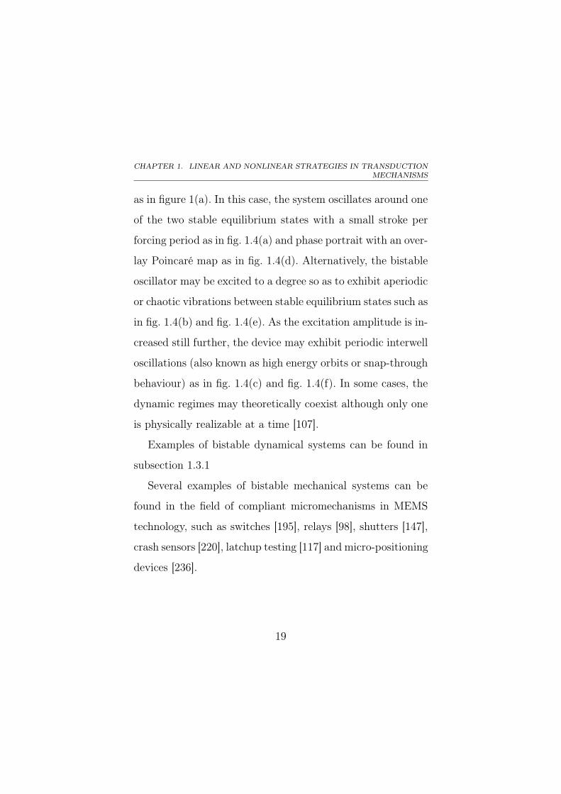
Examples of bistable dynamical systems can be found in
subsection 1.3.1
Several examples of bistable mechanical systems can be
found in the field of compliant micromechanisms in MEMS
technology, such as switches [195], relays [98], shutters [147],
crash sensors [220], latchup testing [117] and micro-positioning
devices [236].
19
1.2. NONLINEAR TRANSDUCTION METHODOLOGIES: BISTABLESTRATEGIES
Fig. 1.4 – Example of displacement–time responses (top row) and phase plots
with an overlap Poincaré map as black circles (bottom row) for three dynamic
regimes of bistable oscillators, as reported in fig. 1.2: (a) and (d) intrawell
oscillations, (b) and (e) chaotic interwell vibrations, (c) and (f) interwell os-
cillations [107].
More details about the applications of bistable systems in
sensing and energy harvesting will be exposed in section 1.3.
20

CHAPTER 1. LINEAR AND NONLINEAR STRATEGIES IN TRANSDUCTIONMECHANISMS
1.3 Applications of bistable strategies:
energy harvesting and sensors
The characteristics of the bistable mechanisms have been
exploited in the field of sensors and energy harvesting to de-
velop innovative solutions and to overcome some limits of tra-
ditional devices, under certain operating conditions [40, 107].
In the following subsections, some of the proposed bistable
strategies in sensors (subsection 1.3.1) and in vibration en-
ergy harvesters (subsection 1.3.2) will be presented along with
some background knowledge on mathematics and physics to
motivate the adoption of these strategies.
Since a bistable AC current sensor is proposed in this work,
a discussion about the state of the art in AC current sensors
and about the benefits of bistability in this field will be ad-
dressed in section 4.1.
More general details about energy harvesting from mechan-
ical vibrations and a discussion about the state of the art in
vibrations microgenerators will be exposed in section 3.1.
21
1.3. APPLICATIONS OF BISTABLE STRATEGIES: ENERGY HARVESTINGAND SENSORS
1.3.1 Applications of bistable mechanisms in sensors
Since the development of the theories on stochastic reso-
nance and on the benefits of the interplay between noise and
nonlinearity, nonlinear dynamics sensors, especially bistable
sensors, have been viewed with interest by scientific commu-
nity [40].
In fact, in some applications where the Signal-to-Noise Ra-
tio (SNR) is too small, signal detection could be quite chal-
lenging, especially for “weak” signals. However, there are cases
where noise, instead of degrading the signal detection, can
enhance the SNR, if principles of stochastic resonance are
applied. This allows the information to be captured by the
sensor, even when the noise floor is high. It has been demon-
strated that the properties of overdamped bistable dynamic
systems can be exploited to develop a novel class of sen-
sors that properly operate in environments with a significant
amount of noise, differently from many devices based on linear
strategies. In addition, the environmental noise can activate
their sensor operation and/or enhance their performance by
interplaying with the nonlinearities in these devices. For this
22
CHAPTER 1. LINEAR AND NONLINEAR STRATEGIES IN TRANSDUCTIONMECHANISMS
reason this kind of detectors has been named “Noise Activated
Nonlinear Dynamic Sensors” [88].
Noise Activated Nonlinear Dynamic Sensors
The operating principle of noise activated sensors can be
understood by considering a bistable dynamic system, whose
generic form is given by (1.4) [40].
x = −∇U(x) (1.4)
where x is the state variable and U(x) is a generic bistable
potential (a plot example is shown in fig. 1.2), which underpins
the behaviour of numerous systems in the physical world such
as electronic circuits (e.g., Schmitt trigger) [210], mechani-
cal systems [116], systems with hysteresis (e.g., ferromagnetic
and ferroelectric materials) [39] and decision-making processes
in cell cycle progression, cellular differentiation, and apopto-
sis [254].
The most studied example is the overdamped Duffing sys-
tem whose potential U(x) is depicted by (1.5) [73].
23
1.3. APPLICATIONS OF BISTABLE STRATEGIES: ENERGY HARVESTINGAND SENSORS
U(x) = −ax2 + bx4 (1.5)
The two parameters a and b determine the shape of the
potential. When a > 0, the potential is bistable with the sta-
ble equilibrium states centered at x = ±√a/(2b), the un-
stable equilibrium state at x = 0 and a potential barrier
U0 = a2/(4b); while for a ≤ 0 the system becomes monos-
table [73].
Another example of nonlinear bistable system is repre-
sented by the Analog Hopfield Neuron potential in (1.6) [114]:
U(x) = ax2 − b ln[cosh(x)
](1.6)
where x denotes a cell membrane voltage and a and b are
parameters conditioning the shape of the potential.
A different example of bistable potential is given by the
RF SQUID loop in (1.7) [43]:
U(x) = ax2b cos(2πx) (1.7)
in which x denotes the magnetic flux in the loop and a and
b are parameters that shape the potential.
24
CHAPTER 1. LINEAR AND NONLINEAR STRATEGIES IN TRANSDUCTIONMECHANISMS
The simplest version of a nonlinear dynamic bistable sys-
tem exhibiting stochastic resonance can be obtained by adding
a time-periodic “deterministic” sinusoidal signal of amplitude
A and frequency fs and a “stochastic” noise F (t) (which is
generally Gaussian and exponentially correlated) to the sys-
tem in (1.4). This leads to the (1.8) [40].
x = −∇U(x) + F (t) + A sin(2πfsx
)(1.8)
In absence of any external forcing (A = 0 and F = 0), the
system in (1.8) will settle near the bottom of one of the two
potential wells.
A more complex behaviour is observed when the exter-
nal time-periodic forcing of period Ts (i.e. Ts = 1/fS) and
the “stochastic” noise are applied to the system (A 6= 0 and
F (t) 6= 0) in (1.8). The time-periodic forcing term causes a
periodic rocking, back and forth, of the potential barriers in
the bistable potential with the same period Ts of the periodic
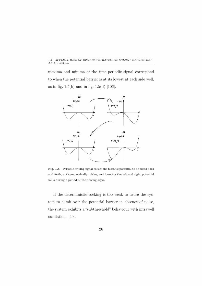
forcing. In a single period of the forcing signal, the poten-
tial is cycled through fig. 1.5(a)–fig. 1.5(d), antisymmetrically
raising and lowering the left and right potential wells. The
25
1.3. APPLICATIONS OF BISTABLE STRATEGIES: ENERGY HARVESTINGAND SENSORS
maxima and minima of the time-periodic signal correspond
to when the potential barrier is at its lowest at each side well,
as in fig. 1.5(b) and in fig. 1.5(d) [106].
Fig. 1.5 – Periodic driving signal causes the bistable potential to be tilted back
and forth, antisymmetrically raising and lowering the left and right potential
wells during a period of the driving signal.
If the deterministic rocking is too weak to cause the sys-
tem to climb over the potential barrier in absence of noise,
the system exhibits a “subthreshold” behaviour with intrawell
oscillations [40].
26
CHAPTER 1. LINEAR AND NONLINEAR STRATEGIES IN TRANSDUCTIONMECHANISMS
The addition of even small amounts of noise, however, can
give a finite switching probability to the system response and,
so, some potential barrier crossings could occur. For moder-
ate noise, the switchings will acquire a degree of coherence
with the underlying time-periodic signal because the switch-
ing probability is maximized whenever the absolute value
of the time-periodic signal is at its maximum, as shown in
fig. 1.5(b) and in fig. 1.5(d).
The barrier crossing rate, thus, depends critically on the
noise intensity. If the noise intensity is very low, the probabil-
ity of any switching occurring is quite tiny. On the other hand,
intense noise can induce switchings even in an “unfavourable”
interval (i.e. when the absolute value time periodic signal is at
its minimum); in this case, the output signal is swamped. In
between, there is a wide range of noise intensities introducing
switching events in near-synchronicity with the applied time-
periodic signal. This cooperation between the deterministic
signal and stochastic noise introduces a certain “coherence” in
the system.
27
1.3. APPLICATIONS OF BISTABLE STRATEGIES: ENERGY HARVESTINGAND SENSORS
This “coherence” in the system can be recognized by ob-
serving the SNR of the system as a function of the magni-
tude of the input stochastic noise. A peak in the SNR can
be found at a given level of noise: this is the critical point
of maximum coherence in the system. Past this critical noise
strength, the switchings lose coherence with the time-periodic
signal frequency and the dynamics become noise-dominated,
thus decreasing the SNR. The earliest definition of stochastic
resonance is given by the maximum of the signal amplitude
as a function of the noise level [40]. In this case, the noise
enhances the SNR and, thus, improve system performance. It
is worth noted that this phenomenon has been observed also
in monostable [226], multistable and coupled bistable [128]
systems.
This theory coupled with proper readout mechanisms can
be applied to sense quantities in applications where noise and
device sensitivity could be critical.
28
CHAPTER 1. LINEAR AND NONLINEAR STRATEGIES IN TRANSDUCTIONMECHANISMS
Readout schemes for noise activated nonlinear
dynamic sensors
In many cases, the detection of a small target signal (DC
or low frequency) through a bistable system is based on a
spectral technique [34], where a known periodic bias signal is
applied to the sensor to saturate it and drive it very rapidly
between its two (locally) stable attractors (corresponding to
the minima of the bistable potential energy function, when
the attractors are fixed points). Often, the amplitude of the
bias signal is taken to be quite large in order to render the
response largely independent from the noise. The effect of
a target DC signal is, then, to skew the potential, resulting
in the appearance of features at even harmonics of the bias
frequency fs in the system response [25]. The spectral ampli-
tude at 2fs is, then, proportional to the bias frequency and
the square of the target signal amplitude; hence, the spectral
amplitude can be used to yield the target signal. In prac-
tice, a feedback mechanism is frequently utilized for reading
out the asymmetry-producing target signal via a nulling tech-
nique [34]. An example of this readout mechanism via bistable
29
1.3. APPLICATIONS OF BISTABLE STRATEGIES: ENERGY HARVESTINGAND SENSORS
dynamics mechanisms is the second harmonic fluxgate exploit-
ing the bistability descending from saturation in hysteretic
ferromagnetic cores [99].
The above readout scheme has some drawbacks. First of all,
a large onboard power is needed to provide a high-amplitude
and high-frequency bias signal. Furthermore, feedback elec-
tronics can be cumbersome and introduce their own noise floor
into the measurement system. Finally, a high-amplitude and
high-frequency bias signal often increases the noise floor in
the system [88].
A different readout scheme is based on the residence time
statistics in a bistable system. This approach consists in mea-
suring the mean time spent by the system in each of its sta-
ble equilibrium states to both quantify the stochastic reso-
nance phenomenon [40] and gain information on the presence
of small-unknown target signals in sensors field [88].
Given a bistable dynamic system as that formulated in (1.8),
in absence of noise (F (t) = 0) and in presence of the time-
periodic signal (A 6= 0), when the bistable in intrinsically sym-
metric (e.g., the Duffing potential in (1.5)), the two residence
30
CHAPTER 1. LINEAR AND NONLINEAR STRATEGIES IN TRANSDUCTIONMECHANISMS
times will be, on average, identical and, thus their difference
will be zero. The presence of even a small amount of noise
leads to a residence times distribution (RTD) about a mean
value, due to uncertainties in the switching time. The presence
of an external target signal (i.e. the noise F (t) in (1.8)) usually
make the potential asymmetric with a concomitant difference
in the mean residence times. This difference is proportional
to the asymmetry-producing target signal itself.
This procedure has shown some advantages compared to
the aforesaid procedure based on a spectral readout. It has
been implemented experimentally without complicated feed-
back electronics and works with or without the bias signals.
In fact, the difference in residence times is quantifiable even
in the absence of the time-periodic bias signal, when the sen-
sor is driven between its stable equilibrium states by only the
noise, although some practical considerations (e.g., observa-
tion times depending on the relative magnitude of the noise
standard deviation and on the barrier height), may limit the
applicability of this strategy in some practical cases. It has
been demonstrated also that residence-times based technique
31
1.3. APPLICATIONS OF BISTABLE STRATEGIES: ENERGY HARVESTINGAND SENSORS
works fine without the knowledge of the computationally de-
manding power spectral amplitude of the system output (in
most cases a simple averaging procedure on the system output
has worked just fine) and, finally, it has performed well even
in presence of large levels of noise [88].
Applications of these readout scheme are given by RTD
fluxgate magnetometers [14] and electric field sensors based
on ferroelectric materials [13].
An autonomous bistable sensor exploiting the benefit from
nonlinearity and noise for measurement of AC currents and
energy harvesting is proposed in this work and a discussion
about the state of the art of AC current sensors will be dis-
cussed in section 4.1
Threshold sensors
Apart from the applications of the theories on stochastic
resonance, the bistable principle in the field of sensors has
been exploited for detecting when the magnitude of certain
physical quantities under observation exceeds a predefined
threshold (i.e. threshold sensors). In these applications, when
the threshold is passed, the bistable sensor snaps from one
32
CHAPTER 1. LINEAR AND NONLINEAR STRATEGIES IN TRANSDUCTIONMECHANISMS
of its stable equilibrium state to the other one, returning as
output a status change handled by circuitry.
One of these applications is given by inertial switches [65].
This kind of devices has been thought to detect accelera-
tions that are larger than the threshold imposed by the crit-
ical forces in bistable structures [267]. Their latching opera-
tion and the possibility to properly designing their switching
threshold meet the requirements of some applications, espe-
cially in safety systems, where impulsive accelerations with
large magnitudes descending from crashes and severe impacts
must be handled. In these cases, when overthreshold appli-
cations are detected by snapping from one stable equilibrium
position to the other one, these sensors trigger safety mecha-
nisms (e.g., airbags in cars) to prevent major damages, as an
example, caused by a sudden impact [154]. Other applications
have been found in fuse systems and drop detection systems.
The development of inertial switches in MEMS technologies
has improved their operative range and their response time,
thanks to the downscaling of their geometric dimensions [211].
33
1.3. APPLICATIONS OF BISTABLE STRATEGIES: ENERGY HARVESTINGAND SENSORS
Other examples of threshold sensors are represented by
magnetic [240], flow [169] and thermo-optical sensors [165].
1.3.2 Application of bistable mechanisms in energy
harvesting from vibrations
In the field of energy harvesting from mechanical vibra-
tions, the adoption of bistable devices has been proposed to
improve performance of power generators, at both millimet-
ric and micrometric scale, when wideband vibrational sources
must be addressed.
It is known that ambient mechanical vibrations come in
a large variety of forms such as induced oscillations, seismic
noise, vehicle motion, acoustic noise, multitone vibrating sys-
tems, and, more generally, noisy environments. Sometimes,
the vibrational energy to be collected may be confined in a
very specific region of the frequency spectrum, as in the case
of rotating machines, but very often, energy is distributed over
a wide spectrum of frequencies. In particular, several scenar-
ios exist where a significant fraction of energy is generally
distributed in the lower part of the frequency spectrum, very
often below 500 Hz [200]. This requires energy harvesters hav-
34
CHAPTER 1. LINEAR AND NONLINEAR STRATEGIES IN TRANSDUCTIONMECHANISMS
ing a wideband frequency response at low frequencies in order
to scavenge a larger amount of energy.
Bistable energy harvesters are one of the proposed solu-
tions in literature to broaden the bandwidth at low frequen-
cies of traditional linear resonant oscillating generators, which
offer a good efficiency only when they work around their res-
onant frequency and, consequently, poor performance in out
of resonance operations [161]. For this reason, in their design,
resonant generators require the matching of their frequency
of mechanical resonance with the main frequency of the vi-
brations coming out from the vibrating source.
Differently from resonant devices, bistable mechanical os-
cillators do not require the frequency matching with the
source of mechanical vibrations. This aspect is very impor-
tant because the achievement of very low resonance frequen-
cies (e.g., in the order of a few hundreds of hertz or lower)
with a significantly large quality factor is a challenging is-
sue at microscale and limits the adoption of linear resonant
microgenerators in MEMS technologies [9].
35
1.3. APPLICATIONS OF BISTABLE STRATEGIES: ENERGY HARVESTINGAND SENSORS
The operating regime of periodic interwell oscillations (also
known as high energy orbits or snap-through behaviour) in
bistable systems has been recognized as a means by which
to dramatically improve energy harvesting performance. As
the bistable mechanical system commutates between its sta-
ble equilibrium states, the shuttle (i.e. the inertial mass in
the case of energy harvesters) has to displace a greater dis-
tance from one stable equilibrium state to the other one and
its requisite velocity is much greater than that for intrawell
or chaotic interwell oscillations. Since the electrical output of
an energy harvester is often dependent on the device velocity
(especially in the case of piezoelectric mechanical-to-electrical
transducers), high-energy orbits substantially increase power
per forcing cycle (as compared to intrawell and chaotic in-
terwell oscillations) and are more regular in waveform (as
compared with chaotic oscillations), which is preferable for
external power storage circuits. The output voltage waveform
coming from bistable harvester has been also exploited for
diode-less and zero-threshold solutions for its rectification [95,
150].
36
CHAPTER 1. LINEAR AND NONLINEAR STRATEGIES IN TRANSDUCTIONMECHANISMS
Additionally, snap-through behaviour may be triggered re-
gardless of the form or frequency of exciting vibrations, allevi-
ating concerns about harvesting performance in many realis-
tic vibratory environments dominated by effectively low-pass
filtered excitation [107]. Moreover, the frequency of the inter-
well commutations helps to enlarge the frequency response of
the harvesters, especially at low frequencies (typically below
500 Hz) [17].
One of key limitations of bistable devices in energy harvest-
ing is represented by the necessity of large amounts of input
energy to maintain snap-through behaviour, as it is found in
some of actual devices [107]. Some strategies to decrease the
energy threshold required to switch between stable states have
been developed; one of them consists in a time-periodic forced
excitation mixed with external ambient noisy vibrations [156,
235]. In this particular case, noise effects on device perfor-
mances are considered in the opposite way with respect to
already introduced principle of “noise activated devices” [88].
Noise is no more used to allow the information to be captured
by the sensor but energy harvesting device is aimed to capture
37
1.3. APPLICATIONS OF BISTABLE STRATEGIES: ENERGY HARVESTINGAND SENSORS
the largest amount of energy available in the environment by
lowering the energy threshold barrier for snap-through oper-
ation [235].
Finally, the widespread diffusion of bistable solutions in
integrated devices for energy harvesting is still restrained by
the current difficulties in the implementation of bistable prin-
ciples with microsystem technologies and in the lack of a well
accepted design methodology.
Opposing magnetic forces is one of the strategies very of-
ten used to implement bistable mechanisms. In literature,
there are several solutions based on the magnetic levitation
obtained through permanent magnets having direct [87] or op-
posing [9] magnetization, owing to the possibility to “shape”
the potential energy function of the system by altering the dis-
tance between magnets and, therefore, to “tune” its nonlinear
behaviour. Magnetic strategies are therefore very common in
the area of bistable energy harvesters, however, the presence of
magnets and, in particular, of “moving” magnets is sometimes
not desirable whenever the energy harvester is placed close
to other electronic devices or magnetic sensors that may be
38

CHAPTER 1. LINEAR AND NONLINEAR STRATEGIES IN TRANSDUCTIONMECHANISMS
affected by the fluctuations in the magnetic field. For this rea-
son, some solutions exploiting fully compliant bistable mech-
anisms have been addressed, at the price of complicating the
design of the device [17, 170].
Energy harvesting from mechanical vibrations and the
state of the art in vibrations microgenerators will be discussed
with more details in section 3.1.
39

2
Technologies to fabricate integrated
bistable devices
It is a great profession. There is the satisfaction of watching a figment of
the imagination emerge through the aid of science to a plan on paper. Then
it moves to realization in stone or metal or energy. Then it brings jobs and
homes to men. Then it elevates the standards of living and adds to the comforts
of life. That is the engineer’s high privilege.
Herbert Hoover
In this chapter several technology solutions to fabricate
bistable devices will be presented and discussed. First of all,
consolidated microfabrication processes from MEMS industry
will be introduced, then, rapid prototyping solutions for nan-
otechnology devices and centimeter size components in direct
printing technologies will be proposed.
2.1. MICROELECTROMECHANICAL SYSTEMS (MEMS)
2.1 Microelectromechanical Systems
(MEMS)
Microelectromechanical Systems, or MEMS, represent a
technology field aimed to develop integrated miniaturized
electro-mechanical elements (i.e. microstructures) that are
made using the techniques of microfabrication. The critical
physical dimensions of MEMS devices can vary from well be-
low one micron on the lower end of the dimensional spec-
trum, all the way to several millimeters. Likewise, the types
of MEMS devices can vary from relatively simple structures,
having no moving elements, to extremely complex electrome-
chanical systems with multiple moving elements under the
control of integrated microelectronics. The one main criterion
of MEMS is that there are at least some elements having some
sort of mechanical functionality whether or not these elements
can move [3].
While the functional elements of MEMS are miniatur-
ized structures, sensors, actuators and microelectronics, the
most notable (and perhaps most interesting) elements are mi-
crosensors and microactuators. Microsensors and microactu-
42
CHAPTER 2. TECHNOLOGIES TO FABRICATE INTEGRATED BISTABLEDEVICES
ators are appropriately categorized as “transducers”, which
are defined as devices that convert energy from one form
to another. In the case of microsensors, the device typically
converts a measured mechanical signal into an electrical sig-
nal [131]. Recently, MEMS devices have attracted growing
interest in the field of energy harvesting from mechanical vi-
bration for the opportunity of exploiting displacements and
deformations in microstructures to generate electrical energy
through mechanical-to-electrical transducers for powering low
power devices [158].
Over the past several decades MEMS researchers and de-
velopers have demonstrated an extremely large number of mi-
crosensors for almost every possible sensing modality includ-
ing temperature, pressure, inertial forces, chemical species,
magnetic fields, radiation, etc. Remarkably, many of these
micromachined sensors have demonstrated performances ex-
ceeding those of their macroscale counterparts. For example,
the micromachined version of a pressure transducer, usually
outperforms a pressure sensor made using the most precise
macroscale level machining techniques. Another important
43
2.1. MICROELECTROMECHANICAL SYSTEMS (MEMS)
aspect of MEMS is represented by their method of produc-
tion that exploits (with certain adaptations) the same batch
fabrication techniques used in the integrated circuit indus-
try, which can translate into low per device, as well as many
other benefits. Consequently, it is possible to not only achieve
stellar device performance, but to do so at a relatively low
cost level. Not surprisingly, silicon based discrete microsen-
sors were quickly commercially exploited and the markets for
these devices continue to grow at a rapid rate [242].
The fabrication of MEMS evolved from the process tech-
nology in semiconductor device fabrication, i.e. the basic tech-
niques are deposition of material layers, patterning by pho-
tolithography and etching to produce the required shapes.
Various processes have been developed for the fabrication of
MEMS devices. These processes can be separated into three
main technologies: Bulk Micromachining, Surface Microma-
chining, and LIGA (Lithographie, Galvanoformung, Abfor-
mung) in terms of the strategy to implement released mi-
crostructures [3].
44
CHAPTER 2. TECHNOLOGIES TO FABRICATE INTEGRATED BISTABLEDEVICES
Each technology process has its advantages and limita-
tions. Some of the metrics used to specify the capabilities
of a process are defined as follows [3]:
• minimum linewidth, i.e. the smallest isolated line that can
be reliably patterned;
• minimum spacing, i.e. the smallest patternable gap be-
tween features;
• sidewall profile, i.e. the degree to which an anisotropic etch
deviates from an ideal (vertical) profile;
• layer thicknesses, i.e. the thickness of structural and sacri-
ficial layers;
• aspect ratio, i.e. the ratio between layer thickness and min-
imum linewidth;
• number of mechanical and sacrificial layers.
One of the major goal of this work is to demonstrate
the possibility of using microfabrication techniques to imple-
ment mechanical structures having nonlinear and bistable be-
haviours to be used in vibration energy harvesting and in
nonlinear sensors.
45
2.1. MICROELECTROMECHANICAL SYSTEMS (MEMS)
Nonlinearity in MEMS can be caused through different
strategies. One of them consists in fabricating flexible struc-
tures (e.g., beams, bridges, hinges and so on) having a spe-
cific designed shape to generate nonlinear restoring elastic
forces, as in the case of compliant mechanisms [116]. Another
approach involves the deposition of more “exotic” materials,
such as permanent magnets, sometimes through unconven-
tional techniques to implement nonlinearities [9]. Finally an-
other strategy exploits strains, stresses and nonlinear material
properties to develop nonlinear microstructures like in buck-
led beams [191].
Several MEMS technology processes adopted to design and
develop the nonlinear devices proposed in this work will be
presented in the following.
2.1.1 CNM BESOI process
The BESOI (Bulk and Etch Silicon-On-Insulator) process
is a custom bulk micromachining MEMS technology process
available through the Centro Nacional de Microelectrónica
(CNM) of Barcelona (Spain).
46
CHAPTER 2. TECHNOLOGIES TO FABRICATE INTEGRATED BISTABLEDEVICES
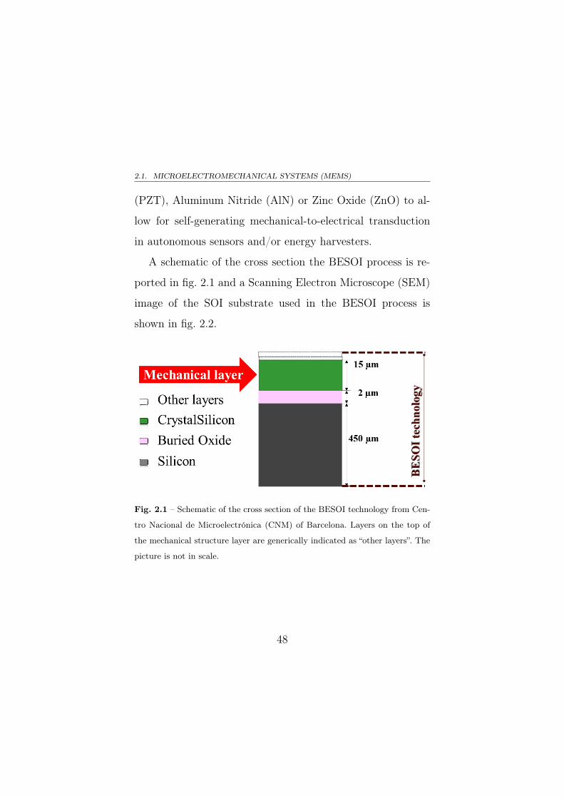
This process starts from an SOI (Silicon-On-Insulator) sub-
strate where the upper 15 µm thick n-doped single crystal
silicon layer acts as primary structural material and also as
electrical connection layer. A 2 µm thick silicon dioxide (SiO2)
layer separates as buried oxide the aforesaid upper single crys-
tal silicon layer from the 450 µm thick n-doped silicon sub-
strate (having <100> orientation).
The release of suspended mechanical structures is per-
formed through both the photolithographic pattern of the up-
per silicon layer from the top and the Reactive Ion Etching
(RIE) of the silicon substrate and of the buried oxide from
the bottom of the wafer.
Depending on the specific application, several thin films of
different materials can be deposited and patterned on the top
of the SOI substrate. As an example, silicon dioxide (SiO2)
can act as electrically and thermally isolating material, alu-
minium and gold as thermal and electrical conductors, poly-
crystalline silicon (or polysilicon) for piezoresistors and so on.
Recently, there is a study to integrate in the process thin
films of piezoelectric materials like Lead Titanate Zirconate
47
2.1. MICROELECTROMECHANICAL SYSTEMS (MEMS)
(PZT), Aluminum Nitride (AlN) or Zinc Oxide (ZnO) to al-
low for self-generating mechanical-to-electrical transduction
in autonomous sensors and/or energy harvesters.
A schematic of the cross section the BESOI process is re-
ported in fig. 2.1 and a Scanning Electron Microscope (SEM)
image of the SOI substrate used in the BESOI process is
shown in fig. 2.2.
Fig. 2.1 – Schematic of the cross section of the BESOI technology from Cen-
tro Nacional de Microelectrónica (CNM) of Barcelona. Layers on the top of
the mechanical structure layer are generically indicated as “other layers”. The
picture is not in scale.
48
CHAPTER 2. TECHNOLOGIES TO FABRICATE INTEGRATED BISTABLEDEVICES
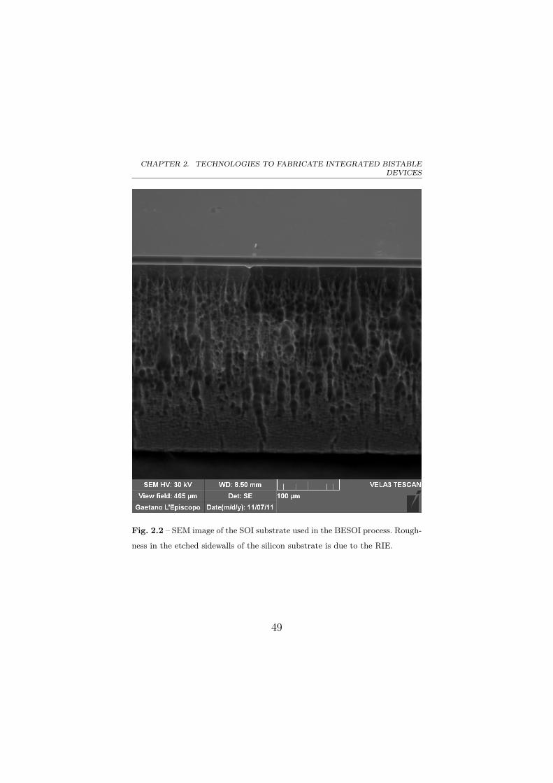
Fig. 2.2 – SEM image of the SOI substrate used in the BESOI process. Rough-
ness in the etched sidewalls of the silicon substrate is due to the RIE.
49
2.1. MICROELECTROMECHANICAL SYSTEMS (MEMS)
This technology process promises interesting performance
because of the possibility to design a large seismic masses with
a tolerable definition of vertical shapes (thanks to the RIE)
from the whole thickness of the wafer.
Examples of applications of this process are given by mi-
croresonators [5], seismometers [16], thermal sensors [10], lat-
eral cantilevers [21] and bistable compliant mechanisms [17].
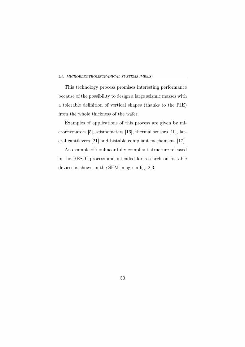
An example of nonlinear fully compliant structure released
in the BESOI process and intended for research on bistable
devices is shown in the SEM image in fig. 2.3.
50
CHAPTER 2. TECHNOLOGIES TO FABRICATE INTEGRATED BISTABLEDEVICES
Fig. 2.3 – SEM image of a nonlinear fully compliant structure released in the
BESOI process.
51
2.1. MICROELECTROMECHANICAL SYSTEMS (MEMS)
2.1.2 MEMSCAPTM MetalMUMPs® process
MetalMUMPs® is a standard commercial process pro-
vided by MEMSCAPTM for the program MUMPs (Multi-User
MEMS Processes) in order to yield cost-effective multi-user
and multi-purpose MEMS fabrication to industry, universi-
ties, and government worldwide.
MetalMUMPs® is an electroplated nickel hybrid microma-
chining process derived from work performed at MEMSCAPTM
throughout the 1990s. This process flow was originally devel-
oped for the fabrication of MEMS micro-relay devices based
on a thermal actuator technology [62], lately it has been ap-
plied to a very wide range of applications in the field of mi-
crosensors [18, 215] and microactuators [45, 94].
A schematic example of the cross section of a device in
MetalMUMPs® process is shown in fig. 2.4.
This process has the following general features:
• 20.5 µm thick electroplated nickel is used as the primary
structural material and electrical interconnect layer.
52
CHAPTER 2. TECHNOLOGIES TO FABRICATE INTEGRATED BISTABLEDEVICES
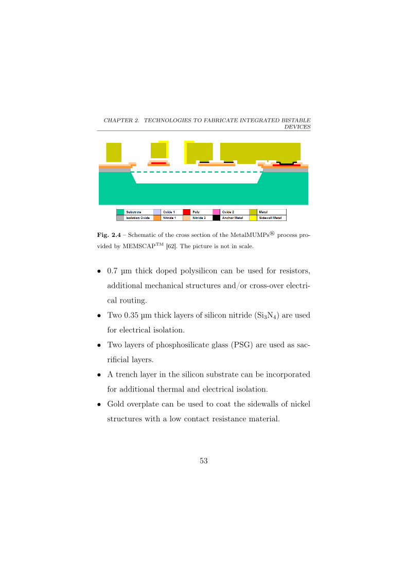
Fig. 2.4 – Schematic of the cross section of the MetalMUMPs® process pro-
vided by MEMSCAPTM [62]. The picture is not in scale.
• 0.7 µm thick doped polysilicon can be used for resistors,
additional mechanical structures and/or cross-over electri-
cal routing.
• Two 0.35 µm thick layers of silicon nitride (Si3N4) are used
for electrical isolation.
• Two layers of phosphosilicate glass (PSG) are used as sac-
rificial layers.
• A trench layer in the silicon substrate can be incorporated
for additional thermal and electrical isolation.
• Gold overplate can be used to coat the sidewalls of nickel
structures with a low contact resistance material.
53

2.1. MICROELECTROMECHANICAL SYSTEMS (MEMS)
• Strategies descending from surface micromachining pro-
cesses (i.e. the use of sacrificial layers) and bulk microma-
chining processes (i.e. the trench etch of silicon substrate)
are adopted to release structures. Micromolding techniques
are adopted to deposit and pattern the electroplated nickel
layer.
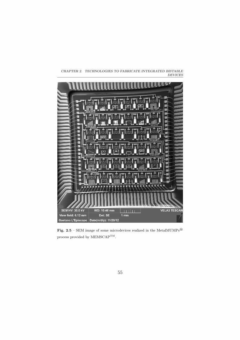
A SEM picture of several devices (microsensors and mi-
croactuators) designed at the University of Catania (Italy)
and realized in this process is reported in fig. 2.5.
Complete process flow and design rules are described in
the documentation provided by MEMSCAPTM [62].
54
CHAPTER 2. TECHNOLOGIES TO FABRICATE INTEGRATED BISTABLEDEVICES
Fig. 2.5 – SEM image of some microdevices realized in the MetalMUMPs®
process provided by MEMSCAPTM.
55
2.1. MICROELECTROMECHANICAL SYSTEMS (MEMS)
2.1.3 MEMSCAPTM PiezoMUMPs® process
Similarly to MetalMUMPs®, PiezoMUMPs® is another
multi-user process provided by MEMSCAPTM under the pro-
gram MUMPs.
PiezoMUMPs® process has been introduced by MEMSCAPTM
during the 2013 and is designed for general purpose microma-
chining of piezoelectric devices in a Silicon-On-Insulator (SOI)
framework for sensors, actuators and energy harvesters [63].
The cross-section of this process is illustrated in the schematic
in fig. 2.6.
A silicon-on-insulator wafer composed of a 10 µm thick
silicon layer, 1 µm thick buried silicon dioxide and 400 µm
thick handle wafer is used as the starting substrate.
The 10 µm thick silicon layer represents both the structural
layer and an electrical connection layer as it is doped during
the process flow.
Similarly to the BESOI process in the subsection 2.1.1, the
SOI substrate of the PiezoMUMPs® process is patterned and
etched from both its top (pattern of the silicon layer) and
56
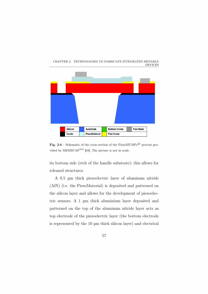
CHAPTER 2. TECHNOLOGIES TO FABRICATE INTEGRATED BISTABLEDEVICES
Fig. 2.6 – Schematic of the cross section of the PiezoMUMPs® process pro-
vided by MEMSCAPTM [63]. The picture is not in scale.
its bottom side (etch of the handle substrate): this allows for
released structures.
A 0.5 µm thick piezoelectric layer of aluminum nitride
(AlN) (i.e. the PiezoMaterial) is deposited and patterned on
the silicon layer and allows for the development of piezoelec-
tric sensors. A 1 µm thick aluminium layer deposited and
patterned on the top of the aluminum nitride layer acts as
top electrode of the piezoelectric layer (the bottom electrode
is represented by the 10 µm thick silicon layer) and electrical
57
2.1. MICROELECTROMECHANICAL SYSTEMS (MEMS)
routing layer. A 0.2 µm thick silicon dioxide layer is used as
electrical isolating layer.
Further details about process flow and design rules are de-
scribed in the documentation provided by MEMSCAPTM [63].
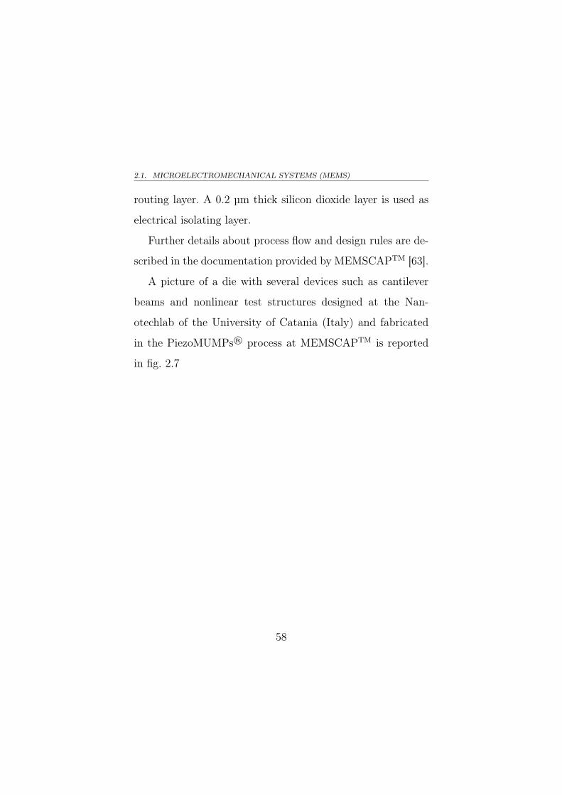
A picture of a die with several devices such as cantilever
beams and nonlinear test structures designed at the Nan-
otechlab of the University of Catania (Italy) and fabricated
in the PiezoMUMPs® process at MEMSCAPTM is reported
in fig. 2.7
58
CHAPTER 2. TECHNOLOGIES TO FABRICATE INTEGRATED BISTABLEDEVICES
Fig. 2.7 – A die with several devices such as cantilever beams and nonlinear
test structures designed at the Nanotechlab of the University of Catania (Italy)
and fabricated in the PiezoMUMPs® process at MEMSCAPTM.
59
2.1. MICROELECTROMECHANICAL SYSTEMS (MEMS)
2.1.4 STMicroelectronics ThELMA® process
ThELMA® is the acronym of “Thick Epitaxial Layer for
Microactuators and Accelerometers” and is a standard pro-
cess developed by STMicroelectronics for its sensors such as
accelerometers and gyroscopes, which have occupied a large
share of the market for mems sensors in recent years [56, 135].
The process involves the fabrication of 2 silicon wafers: one
“Sensor” wafer which includes microelectromechanical compo-
nents and one “Cap” wafer as sealing element at wafer level.
The two wafers are “bonded” together in the final steps of the
process through wafer-to-wafer bonding (glassfrit or anodic
bonding). The cap wafer is needed to protect the microelec-
tromechanical elements in the sensor wafer inside a sealed
environment. It enables the use of standard microelectronics
back-end technologies like testing, dicing and packaging and
assures the reliability of the product overtime [183].
A schematic of the cross section of the ThELMA® process
is illustrated in fig. 2.8.
Referring to the sensor wafer, ThELMA® is a surface
micromachining process which adopts thick epitaxial doped
60
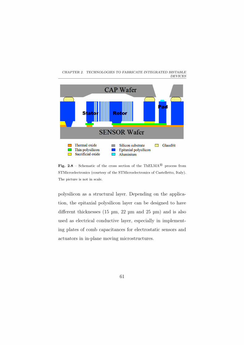
CHAPTER 2. TECHNOLOGIES TO FABRICATE INTEGRATED BISTABLEDEVICES
Fig. 2.8 – Schematic of the cross section of the ThELMA® process from
STMicroelectronics (courtesy of the STMicroelectronics of Castelletto, Italy).
The picture is not in scale.
polysilicon as a structural layer. Depending on the applica-
tion, the epitaxial polysilicon layer can be designed to have
different thicknesses (15 µm, 22 µm and 25 µm) and is also
used as electrical conductive layer, especially in implement-
ing plates of comb capacitances for electrostatic sensors and
actuators in in-plane moving microstructures.
61
2.1. MICROELECTROMECHANICAL SYSTEMS (MEMS)
A 1.1 µm thick silicon dioxide layer is used as sacrificial
layer to release epitaxial polysilicon structures according to
surface micromachining techniques.
A 0.9 µm thin layer of heavily doped polysilicon is adopted
as a conductive layer and for the electrical routing of mi-
croelectromechanical elements. The air-separation of 1.1 µm
(due to the sacrificial silicon dioxide) between thick epitaxial
polysilicon and thin polysilicon (two electrically conductive
layers) generates a capacitance which changes its value when
epitaxial polysilicon structures displace in the out-of-plane di-
rection; for this reason this capacitance is exploited to sense
electrostatically structural displacements in the out-of plane
direction [234].
Pads are implemented through a 0.7 µm thick layer of alu-
minium and silicon substrate in the sensor wafer is protected
through a 2.5 µm thick layer of thermal silicon dioxide.
Some SEM pictures of ThELMA® devices are reported in
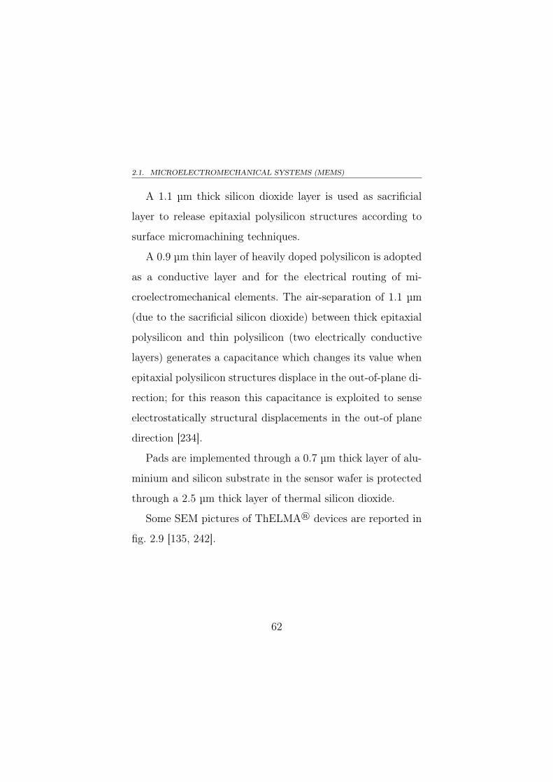
fig. 2.9 [135, 242].
62
CHAPTER 2. TECHNOLOGIES TO FABRICATE INTEGRATED BISTABLEDEVICES
Fig. 2.9 – SEM pictures of some devices in the ThELMA® process from
STMicroelectronics [135, 242].
63
2.1. MICROELECTROMECHANICAL SYSTEMS (MEMS)
2.1.5 Radiant pMEMs® process
Radiant is a company from Albuquerque (NM, USA) spe-
cialized in the fabrication of integrated ferroelectric devices. A
specific fabrication process named “RTI 5µ®” has been devel-
oped by Radiant in order to implement a piezoelectric stack
composed of a thin film of Lead Titanate Zirconate (PZT)
and two platinum electrodes (one on the top and one on the
bottom of the piezoelectric layer) for integrated ferroelectric
capacitors (where top and bottom electrodes are the capacitor
plates and the PZT is the dielectric) [12].
The nominal thickness of the PZT in about 250 nm; top
and bottom platinum electrodes are about 150 nm thick.
The piezoelectric stack is patterned on a 500 nm thick
silicon dioxide used to electrically and thermally isolate the
piezoelectric stack from the underlying silicon substrate.
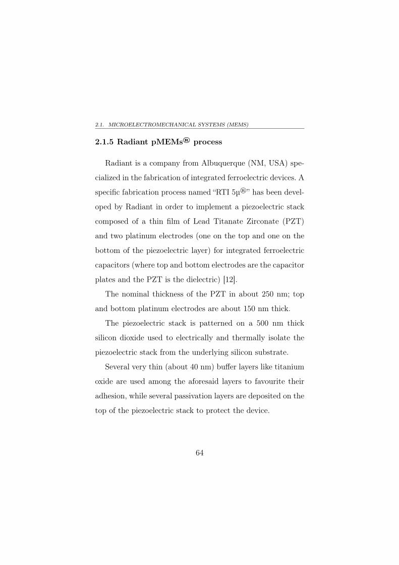
Several very thin (about 40 nm) buffer layers like titanium
oxide are used among the aforesaid layers to favourite their
adhesion, while several passivation layers are deposited on the
top of the piezoelectric stack to protect the device.
64
CHAPTER 2. TECHNOLOGIES TO FABRICATE INTEGRATED BISTABLEDEVICES
Metal pads for electrical interconnections are implemented
by an alloy of chromium and gold.
A schematic of the cross section of the RTI 5µ® process
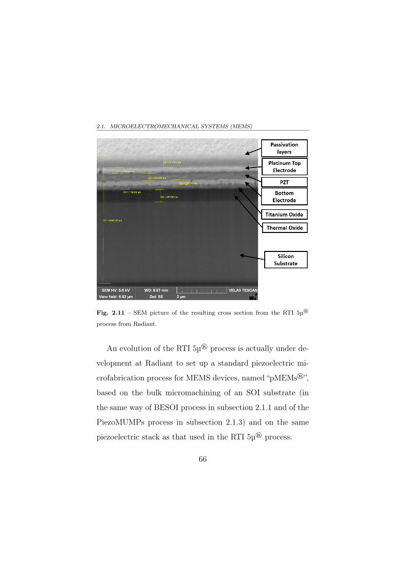
from Radiant is illustrated in fig. 2.10 and an SEM picture
of the cross section resulting from the process is shown in
fig. 2.11.
Fig. 2.10 – Schematic of the cross section of the RTI 5µ® process from
Radiant (courtesy of Radiant inc.). The picture is not in scale.
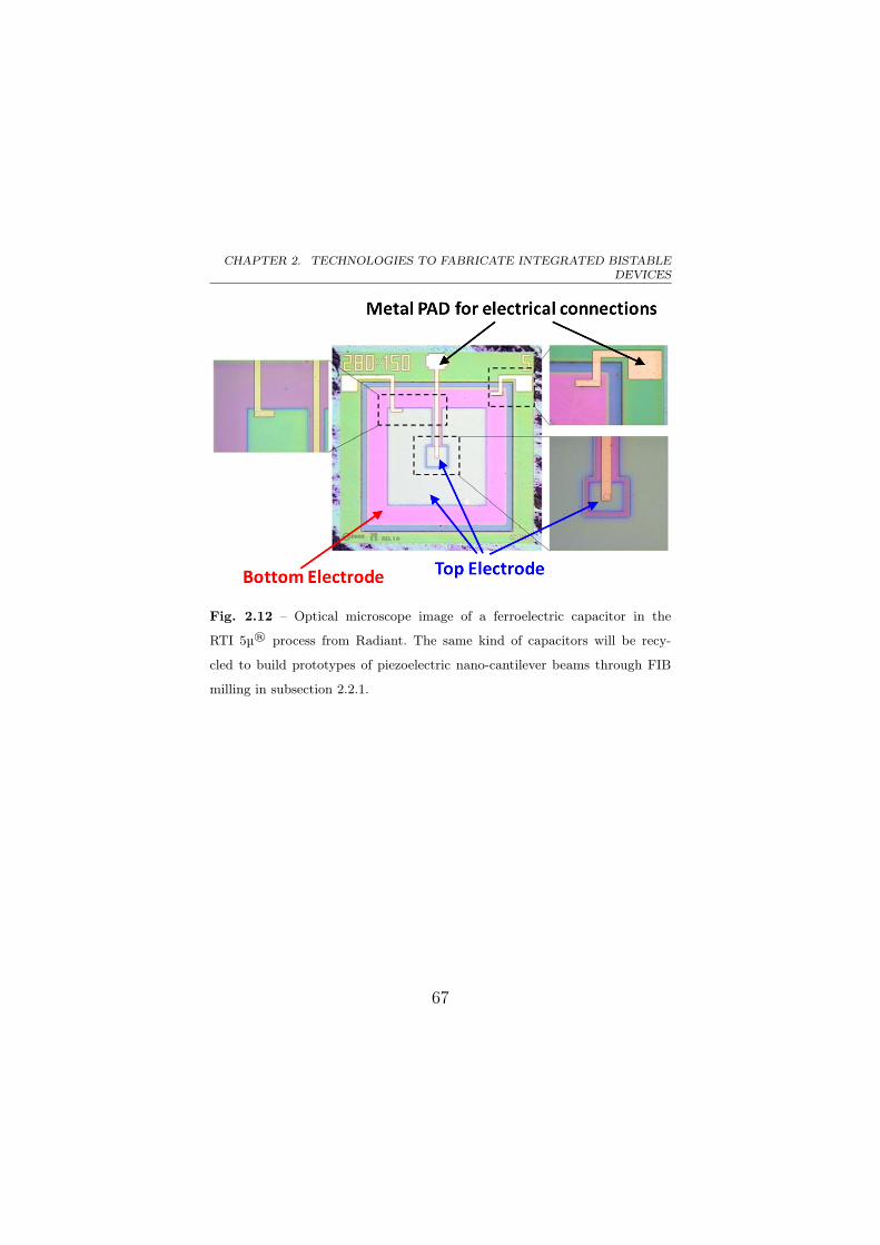
The ferroelectric capacitors in RTI 5µ® have been previ-
ously used for electric field sensing applications [12, 13], and,
in this work, they have been recycled for rapid prototyping of
FIB machined piezoelectric nano-cantilever beams discussed
in subsection 2.2.1. An example of one of these ferroelectric ca-
pacitors is shown in the optical microscope image in fig. 2.11.
65
2.1. MICROELECTROMECHANICAL SYSTEMS (MEMS)
Fig. 2.11 – SEM picture of the resulting cross section from the RTI 5µ®
process from Radiant.
An evolution of the RTI 5µ® process is actually under de-
velopment at Radiant to set up a standard piezoelectric mi-
crofabrication process for MEMS devices, named “pMEMs®”,
based on the bulk micromachining of an SOI substrate (in
the same way of BESOI process in subsection 2.1.1 and of the
PiezoMUMPs process in subsection 2.1.3) and on the same
piezoelectric stack as that used in the RTI 5µ® process.
66
CHAPTER 2. TECHNOLOGIES TO FABRICATE INTEGRATED BISTABLEDEVICES
Fig. 2.12 – Optical microscope image of a ferroelectric capacitor in the
RTI 5µ® process from Radiant. The same kind of capacitors will be recy-
cled to build prototypes of piezoelectric nano-cantilever beams through FIB
milling in subsection 2.2.1.
67
2.2. RAPID PROTOTYPING OF DEVICES IN NANOTECHNOLOGY
2.2 Rapid prototyping of devices in
Nanotechnology
Nanotechnology is the ability to manipulate matter at the
atomic or molecular level to make something useful at the
nano-dimensional scale. It consists in the construction and
in the usage of functional structures designed from atomic
or molecular scale with at least one characteristic dimension
measured in nanometers. Their size allows them to exhibit
novel and significantly improved physical, chemical and bio-
logical properties because of their size. For example, when
characteristic structural features are intermediate between
isolated atoms and bulk materials in the range of about 1 nm
to 100 nm, these objects often display physical attributes sub-
stantially different from those displayed by either atoms or
bulk materials [184].
Phenomena at the nanometer scale are likely to be a com-
pletely new world. Properties of matter at nanoscale may not
be as predictable as those observed at larger scales. Important
changes in behaviour are caused not only by continuous mod-
ification of characteristics with diminishing size, but also by
68
CHAPTER 2. TECHNOLOGIES TO FABRICATE INTEGRATED BISTABLEDEVICES
the appearance of totally new phenomena such as quantum
confinement (a typical example of which is that the color of
light emitting from semiconductor nanoparticles depends on
their sizes). Designed and controlled fabrication and integra-
tion of nanomaterials and nanodevices is likely to be revolu-
tionary for science and technology [184].
In fact, Nanotechnology can provide unprecedented under-
standing about materials and devices and is likely to impact
many fields. By using structure at nanoscale as a tunable
physical variable, we can greatly expand the range of per-
formance of existing chemicals and materials. Alignment of
linear molecules in an ordered array on a substrate surface
(self-assembled monolayers) can function as a new genera-
tion of chemical and biological sensors. Switching devices and
functional units at nanoscale can improve computer storage
and operation capacity by a huge factor. Entirely new bi-
ological sensors facilitate early diagnostics and disease pre-
vention of cancers. Nanostructured ceramics and metals have
greatly improved mechanical properties, both in ductility and
strength [31].
69

2.2. RAPID PROTOTYPING OF DEVICES IN NANOTECHNOLOGY
Basically, there are two approaches in nanotechnology im-
plementation: the top-down and the bottom-up. In the top-
down approach, devices and structures are made using many
of the same techniques as used in MEMS except they are
made smaller in size, usually by employing more advanced
photolithography (such as electron-beam lithography [180])
and etching methods. The bottom-up approach typically in-
volves deposition, growing, or self-assembly technologies. The
advantages of nano-dimensional devices over MEMS involve
benefits mostly derived from the scaling laws, which can also
present some challenges as well [253].
Nanotechnology is a promising way to put essentially ev-
ery atom or molecule in the place and position desired (i.e.
exact positional control for assembly), to make almost any
structure or material consistent with the laws of physics that
can be specified at the atomic or molecular levels and to have
manufacturing costs not greatly exceeding the cost of the re-
quired raw materials and energy used in fabrication.
Although MEMS and Nanotechnology (also named NEMS,
Nanoelectromechanical Systems) are sometimes cited as sep-
70
CHAPTER 2. TECHNOLOGIES TO FABRICATE INTEGRATED BISTABLEDEVICES
arate and distinct technologies, in reality the distinction be-
tween the two is not so clear-cut. In fact, these two technolo-
gies are highly dependent on one another. The well-known
scanning tunneling-tip microscope (STM) which is used to de-
tect individual atoms and molecules on the nanometer scale
is a MEMS device. Similarly the atomic force microscope
(AFM), which is used to manipulate the placement and po-
sition of individual atoms and molecules on the surface of
a substrate, is a MEMS device as well. In fact, a variety of
MEMS technologies are required in order to interface with the
nano-scale domain [257].
An important aspect of nanotechnology in the research and
development of novel devices is represented by the rapid pro-
totyping techniques exploited to rapidly fabricate individual
nanoscale devices for prototyping future electronic applica-
tions. Instead of being used in mass production, tools like
Scanning Electron Microscope (SEM) and Focused Ion Beam
(FIB) are adopted to rapidly fabricate in research laboratories
prototypes of devices to be experimentally studied for future
applications [133].
71
2.2. RAPID PROTOTYPING OF DEVICES IN NANOTECHNOLOGY
Prototypes can be built from scratch by taking advan-
tage of adapted conventional MEMS processes in conjunction
with novel nanomanufacturing processes (e.g., electron beam
lithography [180], self-assembly [252], nanoimprint lithogra-
phy [55], atomic layer epitaxy [229] and so on) or can be de-
rived from existing MEMS or NEMS devices through modifi-
cations and size reduction (FIB milling and FIB gas-assisted
deposition [224]).
Two techniques for rapid prototyping implemented at the
Nanotechlab of the University of Catania (Italy) will be illus-
trated in the following subsections. In the subsection 2.2.1,
the rapid prototyping of piezoelectric cantilever beams, start-
ing from ferroelectric capacitors in the RTI 5µ® process from
Radiant, through FIB milling [224] will be described, and in
the subsection 2.2.2 a technique of deposition of thin films of
Zinc Oxide through Pulsed Plasma Deposition (PPD) [100]
will be discussed.
2.2.1 FIB milling of nano-cantilever beams
Dual-beam systems combining a Focused Ion Beam (FIB)
with a Scanning Electron Microscope (SEM) in a single instru-
72
CHAPTER 2. TECHNOLOGIES TO FABRICATE INTEGRATED BISTABLEDEVICES
ment provide valuable rapid prototyping capability that can
significantly shorten development times for nanoscale devices
in a variety of applications. The strength of dual-beam sys-
tems in prototyping applications derives from their ability to
simultaneously create and observe structures with nanoscale
resolution. The FIB can remove and deposit material in com-
plex patterns with dimensional control of a few nanometers.
Simultaneous, high resolution SEM imaging of the milling
and deposition processes offers unique control of the pattern-
ing process and provides immediate feedback to the opera-
tor. Successful nanoprototyping requires dedicated patterning
and milling strategies that account for interactions between
the FIB and the substrate in the milling and deposition pro-
cesses. Although FIB prototype devices may have material
characteristics that ultimately preclude their routine use in
the intended application, they can provide a structural or elec-
trical equivalent that permits proof of concept and refinement
of design with much greater speed and lower cost than batch
fabrication techniques [255].
73
2.2. RAPID PROTOTYPING OF DEVICES IN NANOTECHNOLOGY
A rapid prototyping application of dual-beam SEM-FIB
systems has been developed at Nanotechlab of Catania (Italy)
for releasing cantilever beams having a piezoelectric out-
put through FIB milling from ferroelectric capacitors in the
RTI 5µ® process from Radiant.
The structure of the ferroelectric capacitor (plates and fer-
roelectric dielectric) are used as piezoelectric stack. In fact, the
250 nm thick layer of PZT allows for mechanical-to-electrical
conversion and the 150 nm thick top and bottom electrodes of
the ferroelectric capacitors act as electrodes to collect charges
from the PZT due to strains: in this configuration the can-
tilever beam works in d31 mode (see subsection 3.1.7).
An area of the die covered by the piezoelectric stack is se-
lectively exposed to the to ion beam coming from the Tescan
Vela3 SEM-FIB of the Nanotechlab of Catania (Italy) at sev-
eral steps to have a maskless etching by sputtering in the area
“bombarded” by the focused ions.
The intensity of the ion beam, the time of each exposition,
the direction of the beam scanning and the angle between the
the surface of the capacitor and the direction of the ion beam
74
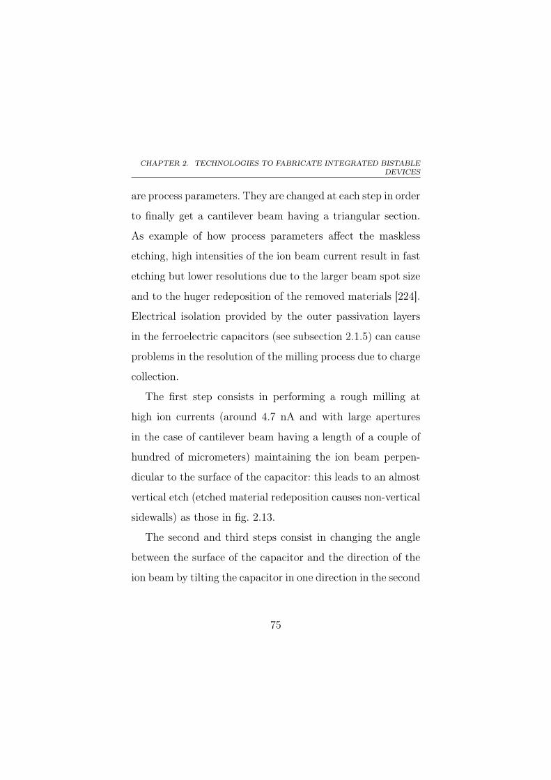
CHAPTER 2. TECHNOLOGIES TO FABRICATE INTEGRATED BISTABLEDEVICES
are process parameters. They are changed at each step in order
to finally get a cantilever beam having a triangular section.
As example of how process parameters affect the maskless
etching, high intensities of the ion beam current result in fast
etching but lower resolutions due to the larger beam spot size
and to the huger redeposition of the removed materials [224].
Electrical isolation provided by the outer passivation layers
in the ferroelectric capacitors (see subsection 2.1.5) can cause
problems in the resolution of the milling process due to charge
collection.
The first step consists in performing a rough milling at
high ion currents (around 4.7 nA and with large apertures
in the case of cantilever beam having a length of a couple of
hundred of micrometers) maintaining the ion beam perpen-
dicular to the surface of the capacitor: this leads to an almost
vertical etch (etched material redeposition causes non-vertical
sidewalls) as those in fig. 2.13.
The second and third steps consist in changing the angle
between the surface of the capacitor and the direction of the
ion beam by tilting the capacitor in one direction in the second
75
2.2. RAPID PROTOTYPING OF DEVICES IN NANOTECHNOLOGY
Fig. 2.13 – First step of process of releasing a cantilever beam through FIB
milling (SEM picture).
76
CHAPTER 2. TECHNOLOGIES TO FABRICATE INTEGRATED BISTABLEDEVICES
step and in the opposed direction in the third step in order
to have an angle below 90° and a sloped excavation to release
the cantilever beam. Typical values of the angle between the
ion beam and the surface of the capacitor are about 10° and
25°, depending on the wanted shape, and this value should
be constant between second and third step in order to get a
symmetric structure at the end of the process. These steps
are performed at high currents (similarly to the first step) to
speed up the prototype process.
The status of the tip of the cantilever beam before and
after its release is shown respectively in the SEM pictures in
fig. 2.14 and in fig. 2.15.
The final result of this process and the sizes of the beam
are reported in figs. 2.16–2.17.
The position of the released cantilever beam inside the die
previously used as ferroelectric capacitor can be observed in
the SEM image in fig. 2.18, along with the three layers of the
piezoelectric stack.
After the release of the beam at the third step, additional
steps could be performed at lower ion currents (typically
77
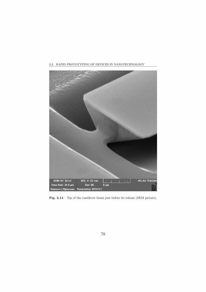
2.2. RAPID PROTOTYPING OF DEVICES IN NANOTECHNOLOGY
Fig. 2.14 – Tip of the cantilever beam just before its release (SEM picture).
78
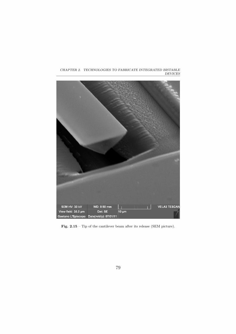
CHAPTER 2. TECHNOLOGIES TO FABRICATE INTEGRATED BISTABLEDEVICES
Fig. 2.15 – Tip of the cantilever beam after its release (SEM picture).
79
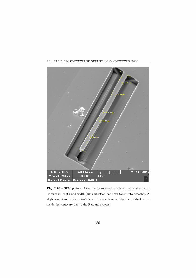
2.2. RAPID PROTOTYPING OF DEVICES IN NANOTECHNOLOGY
Fig. 2.16 – SEM picture of the finally released cantilever beam along with
its sizes in length and width (tilt correction has been taken into account). A
slight curvature in the out-of-plane direction is caused by the residual stress
inside the structure due to the Radiant process.
80
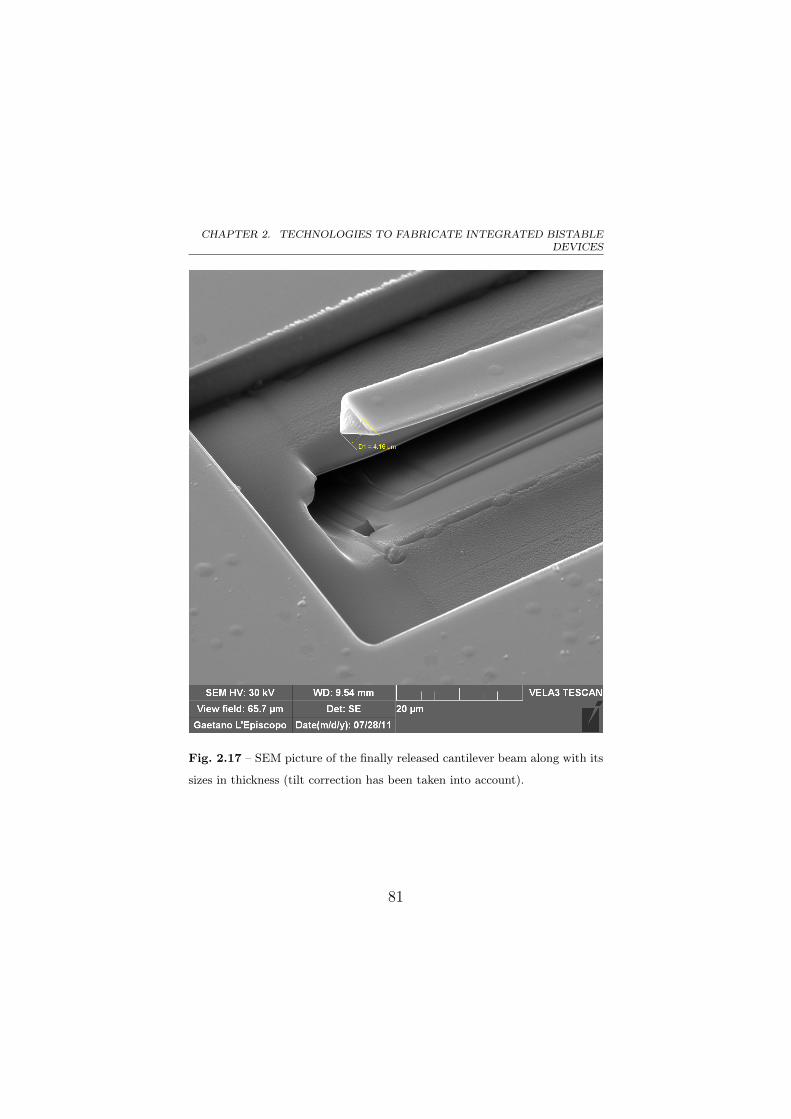
CHAPTER 2. TECHNOLOGIES TO FABRICATE INTEGRATED BISTABLEDEVICES
Fig. 2.17 – SEM picture of the finally released cantilever beam along with its
sizes in thickness (tilt correction has been taken into account).
81

2.2. RAPID PROTOTYPING OF DEVICES IN NANOTECHNOLOGY
Fig. 2.18 – SEM picture illustrating the position of released cantilever beam
inside the die previously used as ferroelectric capacitor. The areas occupied by
the layers of the piezoelectric stack (top electrode, PZT and bottom electrode)
are distinguished by the different shades of gray and indicated in the image
for the sake of clearness.
82
CHAPTER 2. TECHNOLOGIES TO FABRICATE INTEGRATED BISTABLEDEVICES
around a a few hundreds of picoAmpère) to “polish” small
imperfections and tolerances from the previous steps and/or
to obtain wanted sizes (e.g., making thinner the cantilever
beam or reducing its triangular shape) like achieving nano-
metric dimensions such as the cantilever beam shown in the
SEM pictures in figs. 2.19–2.20.
This rapid prototyping technique allows the realization of
piezoelectric cantilever beams having desired dimensions and
shapes by precisely controlling the focused ion beam parame-
ters. These devices can be used as nanotransducers for sensing
applications (after the realization of a application-dependent
functional area on the free end of the beam [217]) or for
nanoactuators (a video of one of these cantilever beams, ac-
tuated by a sinusoidal voltage at 1 Hz is available on inter-
net [142]).
The deposition of thin layers of permanent magnets [51,
155] on the free end of these cantilever beams and near
the beam can allow for the realization of nonlinear devices
through the magnetic levitation as in some macro and micro-
metric examples proposed in literature [6, 9].
83
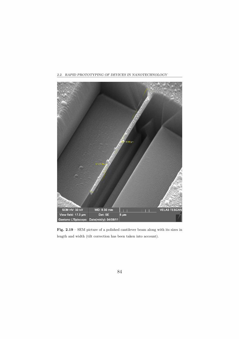
2.2. RAPID PROTOTYPING OF DEVICES IN NANOTECHNOLOGY
Fig. 2.19 – SEM picture of a polished cantilever beam along with its sizes in
length and width (tilt correction has been taken into account).
84
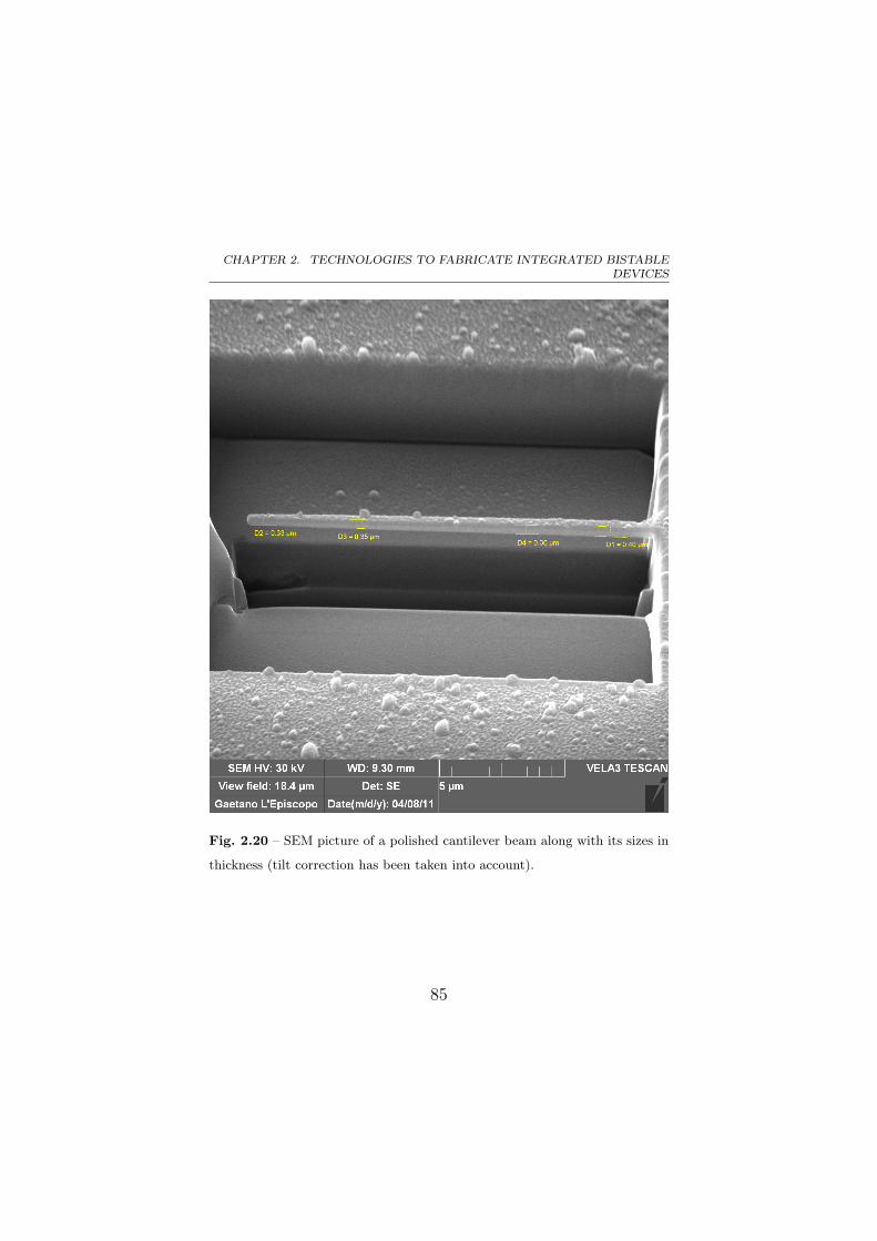
CHAPTER 2. TECHNOLOGIES TO FABRICATE INTEGRATED BISTABLEDEVICES
Fig. 2.20 – SEM picture of a polished cantilever beam along with its sizes in
thickness (tilt correction has been taken into account).
85
2.2. RAPID PROTOTYPING OF DEVICES IN NANOTECHNOLOGY
2.2.2 Deposition of Zinc Oxide through Pulsed
Plasma Deposition
Pulsed Plasma Deposition (PPD) is a Physical Vapor De-
position (PVD) technique to produce thin films (for some
nanometers to several micrometers in thickness) of numerous
materials such as oxides, nitrides, carbides and semiconduc-
tors [100].
The process exploits plasma generated through voltage
pulses (around 40 kV with a few Hertz of frequency) from a
source gas (e.g., oxygen). This plasma is accelerated through
a voltage around 14 kV, oriented and directed, through a di-
electric channel of glass or quartz, towards a grounded target
(containing the target material to deposit) with enough en-
ergy density and power to cause a sub-surface explosion that
projects, for sputtering, vaporized target material outward
(ablation process or sublimation by explosion). The ablated
material is ejected in the form of neutral or ionized atoms,
molecules, radicals, cluster of atoms in amorphous or crys-
talline aggregates, whose spatial distribution can be seen as
a cone with its axis perpendicular to the target surface. This
86
CHAPTER 2. TECHNOLOGIES TO FABRICATE INTEGRATED BISTABLEDEVICES
sort of feather of material named “plume” reaches the sub-
strate which is fixed at an appropriate position (characterized
by and distance and an angle from the target material), quite
close in order to intercept the emission conoid and to allow
the material deposition in a form of thin film on the target
substrate.
All the phases of the process are carried out inside a closed
chamber, named “PPD chamber”, where pressure, tempera-
ture and gases concentration are controlled. The temperature
of the substrate is controlled too. A system to prevent un-
wanted deposition on the target substrate by covering it, es-
pecially when the PPD machine is not in its steady state
operation, has been installed.
Because ablation happens out of the thermodynamic equi-
librium, stoichiometric composition of compounds is kept.
The process of target material ablation is illustrated in the
schematic in fig. 2.21 [100].
A picture of the components of the PPD inside the PPD
chamber along with the pulsed plasma and the plume during
a material deposition is reported in fig. 2.22.
87
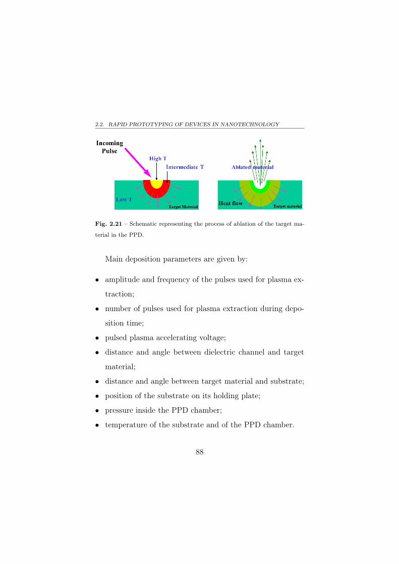
2.2. RAPID PROTOTYPING OF DEVICES IN NANOTECHNOLOGY
Fig. 2.21 – Schematic representing the process of ablation of the target ma-
terial in the PPD.
Main deposition parameters are given by:
• amplitude and frequency of the pulses used for plasma ex-
traction;
• number of pulses used for plasma extraction during depo-
sition time;
• pulsed plasma accelerating voltage;
• distance and angle between dielectric channel and target
material;
• distance and angle between target material and substrate;
• position of the substrate on its holding plate;
• pressure inside the PPD chamber;
• temperature of the substrate and of the PPD chamber.
88
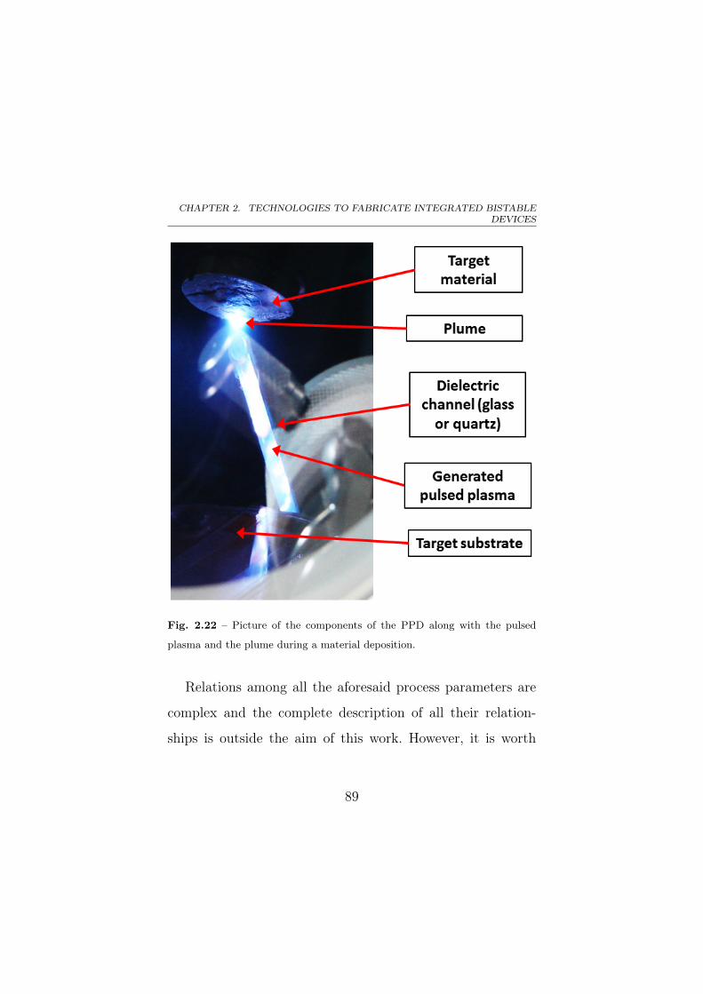
CHAPTER 2. TECHNOLOGIES TO FABRICATE INTEGRATED BISTABLEDEVICES
Fig. 2.22 – Picture of the components of the PPD along with the pulsed
plasma and the plume during a material deposition.
Relations among all the aforesaid process parameters are
complex and the complete description of all their relation-
ships is outside the aim of this work. However, it is worth
89
2.2. RAPID PROTOTYPING OF DEVICES IN NANOTECHNOLOGY
noting only that the thickness of the deposited material layer
is strongly affected by the number of plasma pulses used dur-
ing the deposition process, by their accelerating voltage and
by the pressure inside the PPD chamber. Substrate tempera-
ture plays an important role in the properties of the deposited
material, as explained in the following.
A PPD machine is available at the Nanotechlab of the Uni-
versity of Catania (Italy) and has been exploited to deposit
thin films of Zinc Oxide (ZnO) to be used as piezoelectric
layers in a process step of rapid prototyping applications for
micro e nano-devices.
The objective of the work presented in this subsection is
the setup of the PPD machine to deposit ZnO layers hav-
ing a controlled thickness and a uniform crystalline orien-
tation to provide piezoelectric mechanical-to-electrical trans-
duction. The patterning of the ZnO films, the realization of
proper metal electrodes for readout and of the release of me-
chanical structures are currently under development in sepa-
rated research projects at the Nanotechlab of the University of
Catania (Italy). A studied and implemented rapid prototyp-
90
CHAPTER 2. TECHNOLOGIES TO FABRICATE INTEGRATED BISTABLEDEVICES
ing strategy to release suspended structures (e.g., cantilever
beams having triangular section) based on FIB milling and
compatible with this process has been presented in subsec-
tion 2.2.1.
Piezoelectricity in ZnO films is strictly related to their crys-
talline structure and in particular to its orientation, when ZnO
exhibits wurtzite structure. Studies in literature have shown
that deposition temperature strongly affects the orientation
of wurtzite crystals in ZnO. Higher uniformity in crystalline
orientation leads to improved quality in the piezoelectric prop-
erties of ZnO [265]. For this reason deposition of ZnO has been
carried out adopting a system for substrate temperature con-
trol.
Quite all the process parameters except substrate temper-
ature and the number of plasma pulses have been fixed at
given values derived from previous experiences in the use of
the PPD machine [100]. Among these parameters, the PPD
chamber pressure has been fixed at 0.2 Pa, the pulsed plasma
accelerating voltage at 14 kV, the frequency of the plasma
pulses at 1 Hz and the plasma extraction voltage at 40 kV.
91
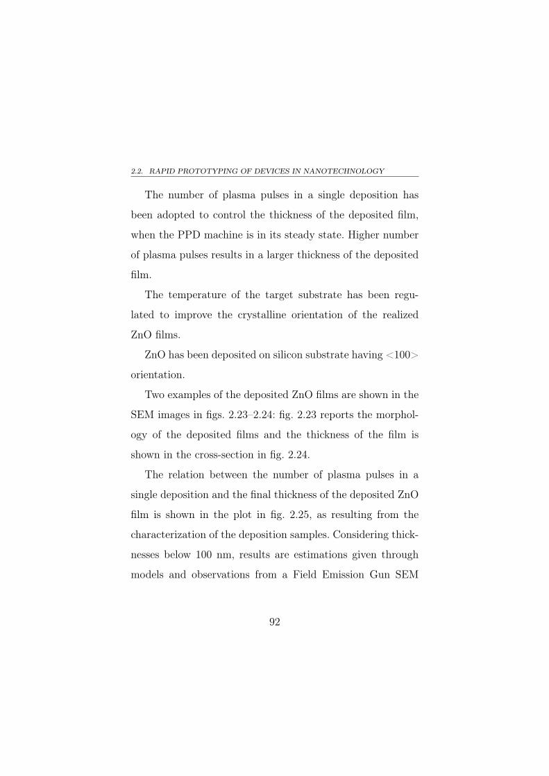
2.2. RAPID PROTOTYPING OF DEVICES IN NANOTECHNOLOGY
The number of plasma pulses in a single deposition has
been adopted to control the thickness of the deposited film,
when the PPD machine is in its steady state. Higher number
of plasma pulses results in a larger thickness of the deposited
film.
The temperature of the target substrate has been regu-
lated to improve the crystalline orientation of the realized
ZnO films.
ZnO has been deposited on silicon substrate having <100>
orientation.
Two examples of the deposited ZnO films are shown in the
SEM images in figs. 2.23–2.24: fig. 2.23 reports the morphol-
ogy of the deposited films and the thickness of the film is
shown in the cross-section in fig. 2.24.
The relation between the number of plasma pulses in a
single deposition and the final thickness of the deposited ZnO
film is shown in the plot in fig. 2.25, as resulting from the
characterization of the deposition samples. Considering thick-
nesses below 100 nm, results are estimations given through
models and observations from a Field Emission Gun SEM
92
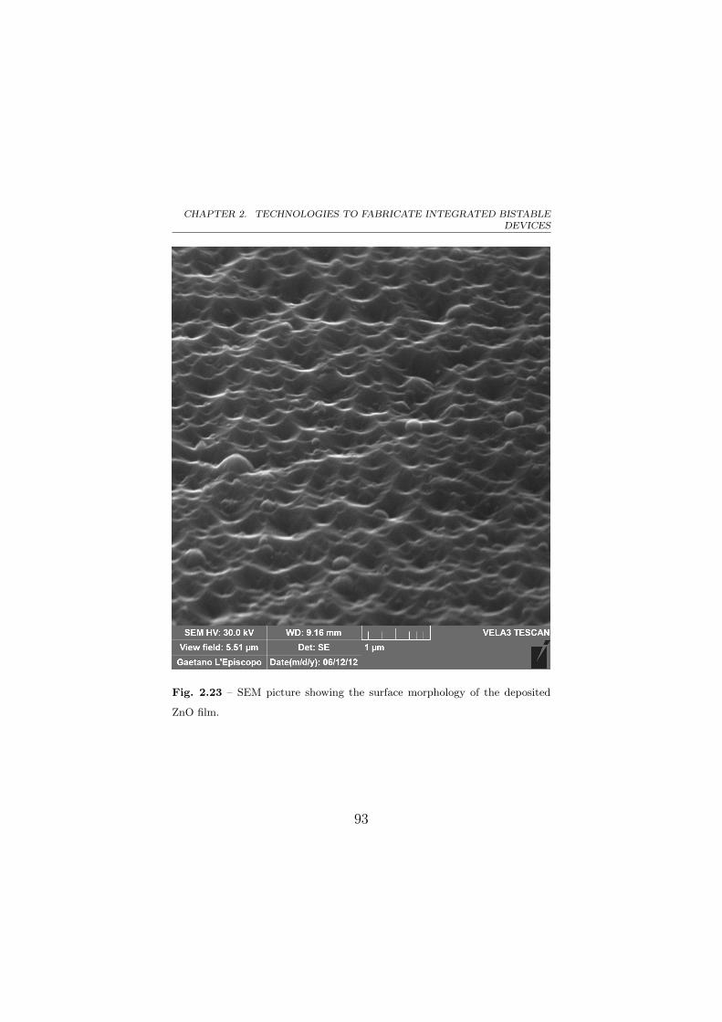
CHAPTER 2. TECHNOLOGIES TO FABRICATE INTEGRATED BISTABLEDEVICES
Fig. 2.23 – SEM picture showing the surface morphology of the deposited
ZnO film.
93
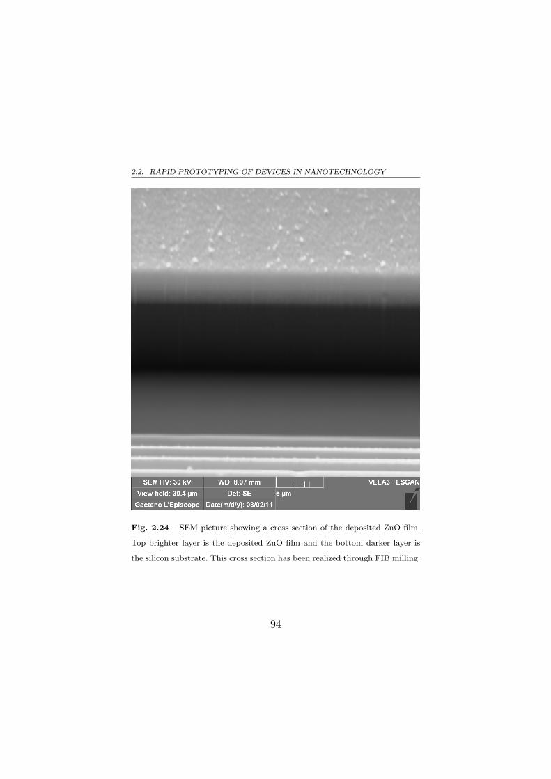
2.2. RAPID PROTOTYPING OF DEVICES IN NANOTECHNOLOGY
Fig. 2.24 – SEM picture showing a cross section of the deposited ZnO film.
Top brighter layer is the deposited ZnO film and the bottom darker layer is
the silicon substrate. This cross section has been realized through FIB milling.
94
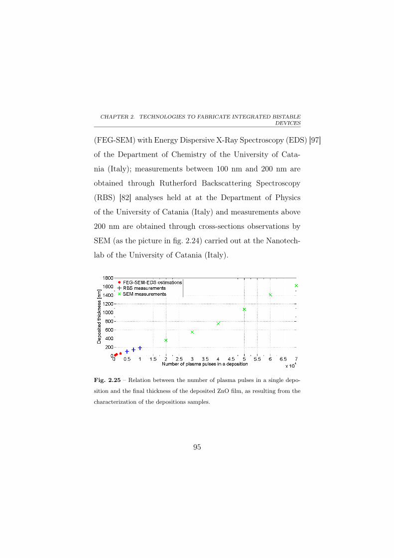
CHAPTER 2. TECHNOLOGIES TO FABRICATE INTEGRATED BISTABLEDEVICES
(FEG-SEM) with Energy Dispersive X-Ray Spectroscopy (EDS) [97]
of the Department of Chemistry of the University of Cata-
nia (Italy); measurements between 100 nm and 200 nm are
obtained through Rutherford Backscattering Spectroscopy
(RBS) [82] analyses held at at the Department of Physics
of the University of Catania (Italy) and measurements above
200 nm are obtained through cross-sections observations by
SEM (as the picture in fig. 2.24) carried out at the Nanotech-
lab of the University of Catania (Italy).
Fig. 2.25 – Relation between the number of plasma pulses in a single depo-
sition and the final thickness of the deposited ZnO film, as resulting from the
characterization of the depositions samples.
95
2.2. RAPID PROTOTYPING OF DEVICES IN NANOTECHNOLOGY
RBS analysis allows for also checking the chemical com-
position of the deposited ZnO layer. As resulting from these
analyses from samples having a thickness between 100 nm and
200 nm, the zinc (Zn) is the 54% of the ZnO compound and
oxygen (O) is the 46%. This confirms the optimum quality
of the deposited compound because these data are not so far
from the ideal 50%–50% stoichiometric ratio of ZnO. One ex-
ample of the RBS spectra obtained from film characterization
is reported in fig. 2.26.
The orientation and the uniformity of the crystalline ori-
entation of the deposited ZnO films have been investigated
through X-Ray Diffraction (XRD) [248] analyses carried out
at the Department of Chemistry of the University of Cata-
nia (Italy). Three different kinds of samples having a thick-
ness of 800 nm have been compared in detector scan XRD
analyses [248]: the first group is represented by ZnO films de-
posited at a substrate temperature of 400℃, the second group
at 600℃ and the third at room temperature. Characterization
results of the comparison are reported in fig. 2.27.
96
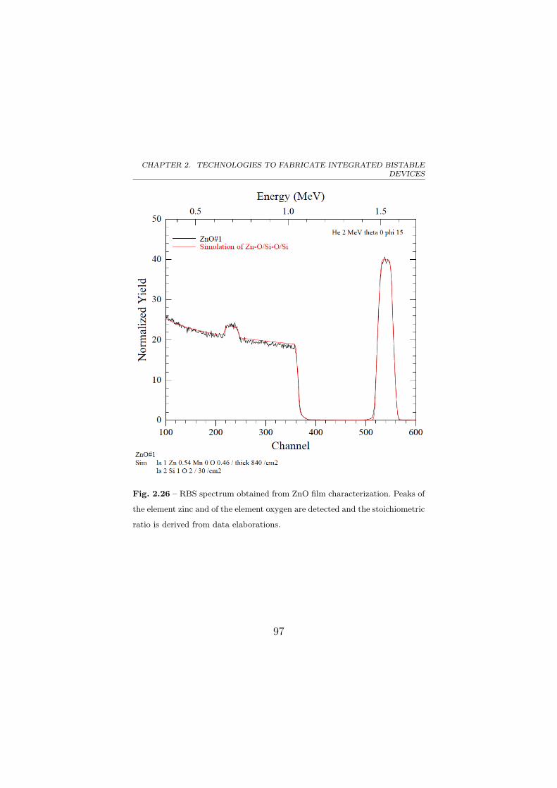
CHAPTER 2. TECHNOLOGIES TO FABRICATE INTEGRATED BISTABLEDEVICES
Fig. 2.26 – RBS spectrum obtained from ZnO film characterization. Peaks of
the element zinc and of the element oxygen are detected and the stoichiometric
ratio is derived from data elaborations.
97
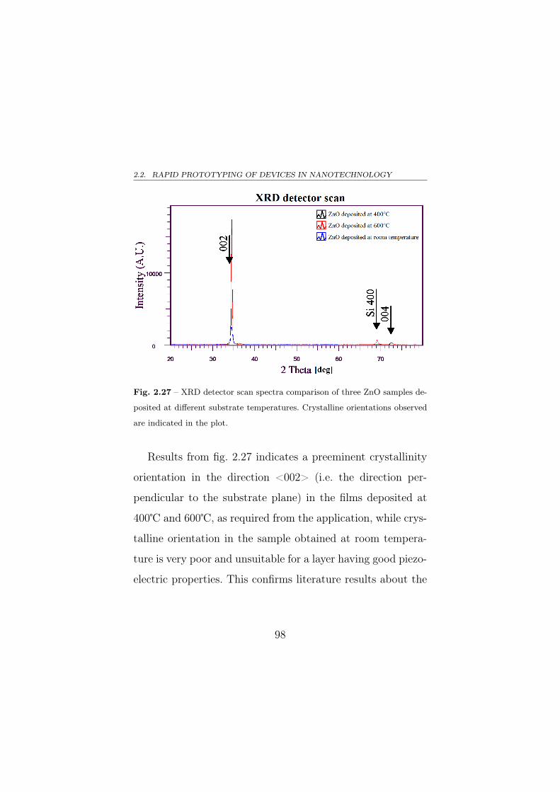
2.2. RAPID PROTOTYPING OF DEVICES IN NANOTECHNOLOGY
Fig. 2.27 – XRD detector scan spectra comparison of three ZnO samples de-
posited at different substrate temperatures. Crystalline orientations observed
are indicated in the plot.
Results from fig. 2.27 indicates a preeminent crystallinity
orientation in the direction <002> (i.e. the direction per-
pendicular to the substrate plane) in the films deposited at
400℃ and 600℃, as required from the application, while crys-
talline orientation in the sample obtained at room tempera-
ture is very poor and unsuitable for a layer having good piezo-
electric properties. This confirms literature results about the
98
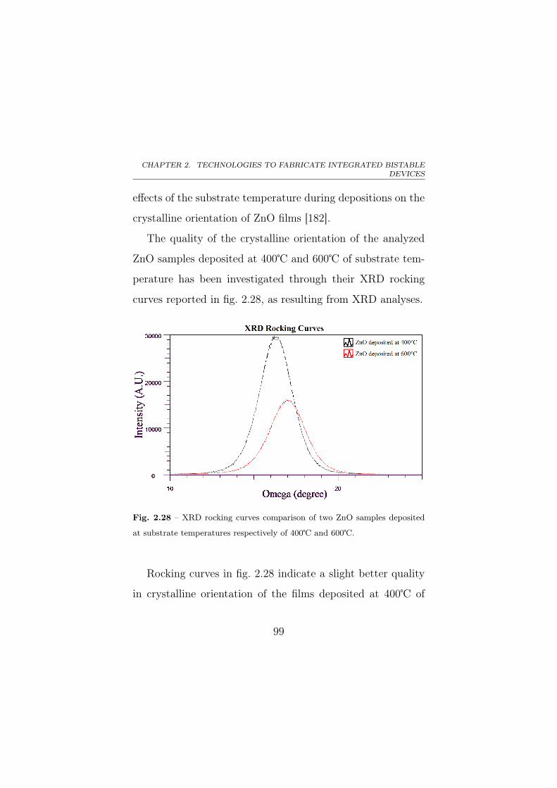
CHAPTER 2. TECHNOLOGIES TO FABRICATE INTEGRATED BISTABLEDEVICES
effects of the substrate temperature during depositions on the
crystalline orientation of ZnO films [182].
The quality of the crystalline orientation of the analyzed
ZnO samples deposited at 400℃ and 600℃ of substrate tem-
perature has been investigated through their XRD rocking
curves reported in fig. 2.28, as resulting from XRD analyses.
Fig. 2.28 – XRD rocking curves comparison of two ZnO samples deposited
at substrate temperatures respectively of 400℃ and 600℃.
Rocking curves in fig. 2.28 indicate a slight better quality
in crystalline orientation of the films deposited at 400℃ of
99
2.3. DEVICES IN DIRECT PRINTING TECHNOLOGY
substrate temperature with respect to samples deposited at
600℃, confirming the suitability of these films for piezoelectric
applications.
2.3 Devices in direct printing technology
In the past decades scientific community has shown a grow-
ing interest in the possibility to make very low-cost electronics
and sensors exploiting technologies coming from the graphic
industry and adopting innovative materials and flexible sub-
strates. This interest is driven by needs for low cost mass-
production processes (e.g., RFID tags, antennas, keyboards,
display and sensors production) [11, 151].
The availability of novel technologies for the development
of low cost and sometimes disposable sensors would move
the market interest towards new applications, previously not
much attractive because of the costs of traditional silicon elec-
tronics. Moreover, the rapid prototyping of cheap devices and
sensors by printing technologies is also of great importance for
the scientific community including research laboratories and
academy.
100
CHAPTER 2. TECHNOLOGIES TO FABRICATE INTEGRATED BISTABLEDEVICES
Among several printing fabrication strategies, screen print-
ing is a technique requiring the use of a mask acting as stencil.
This stencil delimits the areas where ink is free to adhere to
the substrate, following a mechanical pressure exerted typi-
cally through a roller. Examples of sensors realized by screen
printing are: gas detectors exploiting conductive patterns re-
alized by screen printing nanoparticles inks [64], humidity sen-
sors for smart packaging applications [238], impedance sensors
applied to biosensors [37] and resistive force sensors [134].
Given the spread of this technology at a global level, a
good range of conductive, insulating and functional materi-
als, compatible with screen printing, are now commercially
available. Furthermore, screen printing allows to easily obtain
thick layers of material which increases tracks conductivity.
In spite of processes based on photolithography and in gen-
eral requiring masks such as screen printing, inkjet printing
does not require any masks or micromachining. Inkjet print-
ing of polymers and materials is a fairly new technique which
could replace in specific contexts traditional techniques (e.g.
sputtering, lithography, and post-processing). By this drop-
101
2.3. DEVICES IN DIRECT PRINTING TECHNOLOGY
on-demand technique a layer of functional ink can be easily
deposited on the substrate in well defined patterns without
the need of patterning techniques and thus reducing time,
costs and waste of materials. Small volumes of materials, in
the range of 1–30 picoliters, may be filed with a high spatial
resolution and good reproducibility. Moreover, inkjet printing
is a contactless deposition technique which makes it applicable
to many different substrates.
Specifically, inkjet-based sensors offer the possibility to
combine performances of flexible substrates and functional
inks with a cheap rapid prototyping technique. Traditional
materials adopted to realize sensors by inkjet systems are elec-
trical conducting polymers (such as PEDOT-PSS) and func-
tionalized polymers (such as polianiline, PANI).
PEDOT-PSS is a conductive polymer (3,4-ethylen dioxythio-
phene) oxidized with polystyrene sulfonated acid. It is a p-
doped material with a good ambient and thermal stability and
a relatively high electrical conductivity. The use of PEDOT-
PSS to realize conductive patterns requires several printing
102
CHAPTER 2. TECHNOLOGIES TO FABRICATE INTEGRATED BISTABLEDEVICES
cycles in order to reduce the electric resistivity of the pattern
deposited.
Polyaniline (PANI) is a conducting polymer. Many appli-
cations of this material are related to gas sensors. Concerning
its physical properties, it can be dissolved in organic solvents
or in aqueous solutions which are suitable to be used by inkjet
printing.
The implementation of resistors, pads and electrodes by
PEDOT-PSS on PET [222], all-polymer RC filter [146], PANI
based devices for the detection of ammonia [64] and complex
MEMS structures with silver nanoparticles [86] are examples
of devices realized through inkjet techniques.
For what concerns printing equipments, there are various
solutions available on the market allowing for inkjet print-
ing of functional materials [85, 159]. Usually, printer adopting
drop-on-demand mode are used where the ink droplets are
ejected by the use of a pulse generated by thermal or piezo-
electric strategies.
Many printing systems for rapid prototyping are piezoelec-
tric because of their intrinsic suitability when different sol-
103
2.3. DEVICES IN DIRECT PRINTING TECHNOLOGY
vents are used. Systems based on piezoelectric heads provide
resolutions in the order of the tens of micrometers. Usually,
inkjet printers are expensive equipments due to the need for
both printing heads compatibility with different kinds of inks
and the implementation of repeated printing cycles. The latter
is mandatory (e.g., for the realization of conductive patterns
by PEDOT-PSS). It can be observed that the use of expensive
inkjet printing systems allows for the realization of complex
devices.
Actually, one of the main deals using low cost inkjet print-
ing is the nature and the physical property of inks with partic-
ular regards to their viscosity and their electrical properties.
As an example metal based inks (e.g., silver based solutions),
which could play a strategic role for electrodes and sensing
structures due to the extremely low resistivity and mechanic
properties, are difficult to be used with cheap inkjet systems
due to nozzle occlusions problems. Many efforts have been
dedicated to make conductive inks compatible to specifica-
tions required by common inkjet apparatus.
104
CHAPTER 2. TECHNOLOGIES TO FABRICATE INTEGRATED BISTABLEDEVICES
Many examples in the literature adopt a mixed approach
for the realization of low cost devices by direct printing tech-
nology. Conductive structures such as wires, coils, capacitor
electrodes are usually implemented by screen printing tech-
nology. As an example, it must be recalled that the develop-
ment of conductive layers by polymers such as PEDOT-PSS
requires several printing cycles which are not implementable
by low-cost inkjet printers. But, once electrodes have been
realized, polymer layers (such as PEDOT-PSS) for piezore-
sistors, resistive devices and functional layers (such as PANI)
for gas sensors are successively deposited by low cost inkjet
printers. The possibility to use cheap printing systems for the
realization of all inkjet devices (including both electrodes and
other functional layers) would be highly profitable especially
for research laboratories and academy.
In the research field of low-cost printed sensors, the Sensor
Lab of the University of Catania (Italy) has developed a cheap
solution for rapid prototyping of printed devices having sizes
of several centimeters for sensors [15] and nonlinear energy
harvesters [4] through an ordinary commercial piezo inkjet
105

2.3. DEVICES IN DIRECT PRINTING TECHNOLOGY
printer from EPSON®, a conductive ink and a plastic flexible
substrate.
The metal ink used in the realization of the conductive
pattern in these devices is the silver nano-particles solution
“Metalon® JS-B15P” by Novacentrix® [172]. An SEM image
showing the surface morphology and the typical thickness of
the metal ink after its deposition through the inkjet printer
on the plastic flexible substrate is reported in fig. 2.29.
The substrate adopted in the printing is given by the
“NoveleTM IJ-220 coated PET” from Novacentrix®, a treated
polymer film based on polyethylene terephthalate (PET) hav-
ing electrical isolating properties and coated on one of its sides
to allow for a proper and reliable adhesion of metal ink on the
substrate during the printing process. The coating on one of
the two sides of the substrate allows to print metal electrodes
only on the coated side. The thickness of the substrate is
about 165 µm. A SEM picture showing the cross section of
this substrate is reported in fig. 2.30 and the coating is visible
at the top side of the substrate.
106
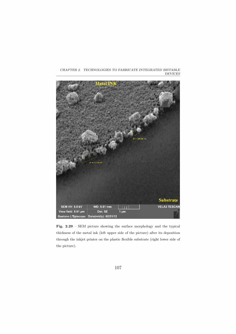
CHAPTER 2. TECHNOLOGIES TO FABRICATE INTEGRATED BISTABLEDEVICES
Fig. 2.29 – SEM picture showing the surface morphology and the typical
thickness of the metal ink (left upper side of the picture) after its deposition
through the inkjet printer on the plastic flexible substrate (right lower side of
the picture).
107
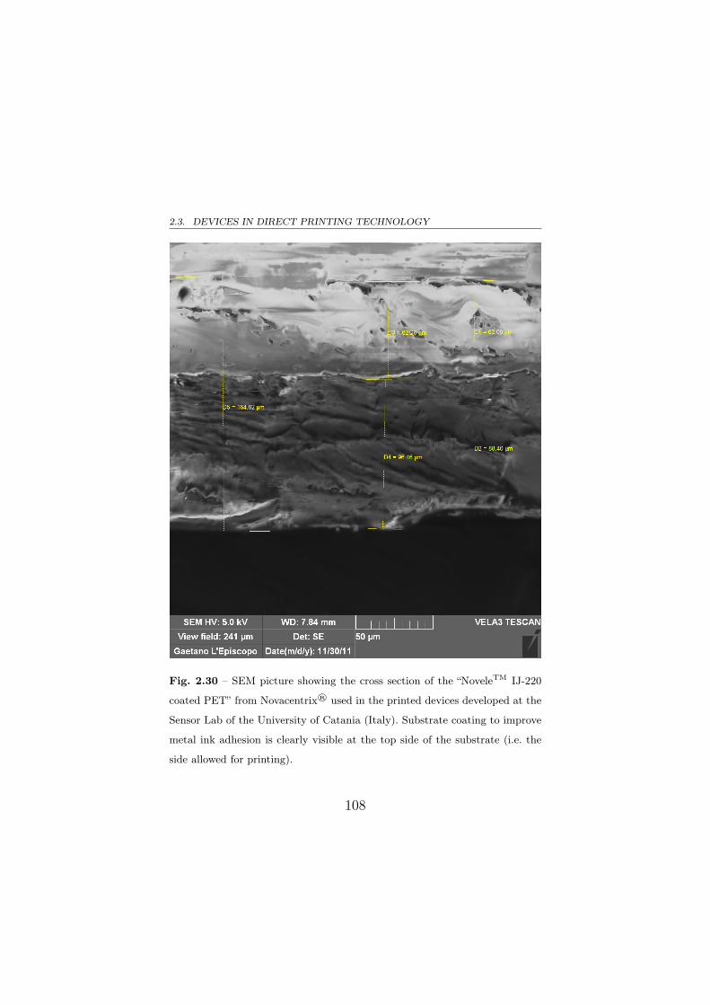
2.3. DEVICES IN DIRECT PRINTING TECHNOLOGY
Fig. 2.30 – SEM picture showing the cross section of the “NoveleTM IJ-220
coated PET” from Novacentrix® used in the printed devices developed at the
Sensor Lab of the University of Catania (Italy). Substrate coating to improve
metal ink adhesion is clearly visible at the top side of the substrate (i.e. the
side allowed for printing).
108
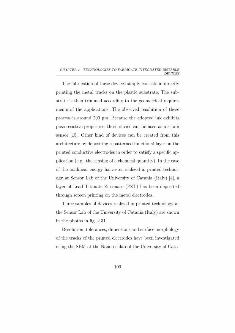
CHAPTER 2. TECHNOLOGIES TO FABRICATE INTEGRATED BISTABLEDEVICES
The fabrication of these devices simply consists in directly
printing the metal tracks on the plastic substrate. The sub-
strate is then trimmed according to the geometrical require-
ments of the applications. The observed resolution of these
process is around 200 µm. Because the adopted ink exhibits
piezoresistive properties, these device can be used as a strain
sensor [15]. Other kind of devices can be created from this
architecture by depositing a patterned functional layer on the
printed conductive electrodes in order to satisfy a specific ap-
plication (e.g., the sensing of a chemical quantity). In the case
of the nonlinear energy harvester realized in printed technol-
ogy at Sensor Lab of the University of Catania (Italy) [4], a
layer of Lead Titanate Zirconate (PZT) has been deposited
through screen printing on the metal electrodes.
Three samples of devices realized in printed technology at
the Sensor Lab of the University of Catania (Italy) are shown
in the photos in fig. 2.31.
Resolution, tolerances, dimensions and surface morphology
of the tracks of the printed electrodes have been investigated
using the SEM at the Nanotechlab of the University of Cata-
109
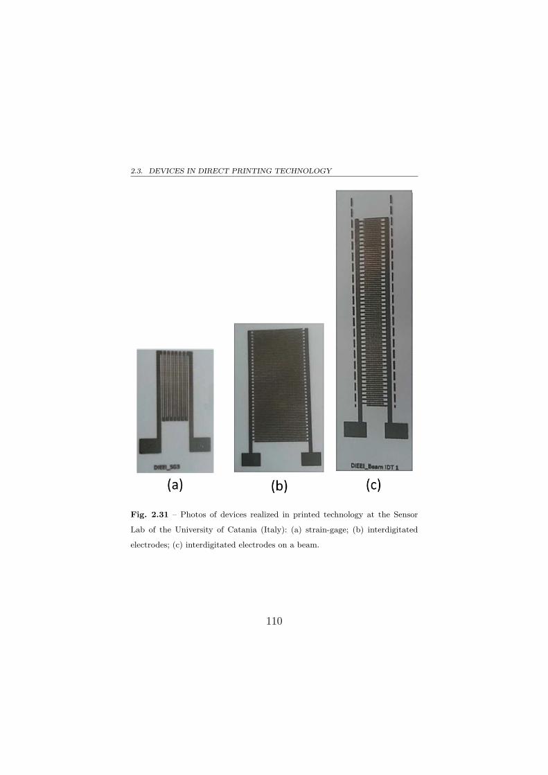
2.3. DEVICES IN DIRECT PRINTING TECHNOLOGY
Fig. 2.31 – Photos of devices realized in printed technology at the Sensor
Lab of the University of Catania (Italy): (a) strain-gage; (b) interdigitated
electrodes; (c) interdigitated electrodes on a beam.
110

CHAPTER 2. TECHNOLOGIES TO FABRICATE INTEGRATED BISTABLEDEVICES
nia (Italy). An example of the SEM images used in this study
is shown in fig. 2.32.
111
2.3. DEVICES IN DIRECT PRINTING TECHNOLOGY
Fig. 2.32 – Example of the SEM images used for the inspection of the res-
olution, tolerances, dimensions and surface morphology of the tracks of the
printed electrodes. Dimensions are shown in the image and effects of the ink
bubbles coming from the printing process are clearly visible.
112

3
Bistable devices for vibration energy
harvesting
Nothing is lost, nothing is created, everything is transformed.
Antoine Laurent de Lavoisier
In this chapter, after an overview about the state of the art
in the field of energy harvesting from mechanical vibrations,
several solutions based on bistable oscillators will be proposed
to scavenge energy from vibrations in a more efficient way
than traditional approaches exploiting linear resonators.
3.1. ENERGY HARVESTING FROM VIBRATIONS: STATE OF THE ART
3.1 Energy harvesting from vibrations: state
of the art
Energy Harvesting (also known as Power Harvesting or En-
ergy Scavenging) is a scientific discipline that deals with the
scavenging of energy (which would otherwise be lost) from one
or more free ambient energy sources (such as sunlight, the me-
chanical vibrations, thermal gradients), its transduction into
an electrical form and its accumulation for later uses.
Differently from photovoltaic and aeolic systems, which de-
liver high amounts of power (e.g., in the order of kilowatts and
megawatts) on large scale for civil and industrial use, energy
harvesting is dedicated to provide small amounts of power
(e.g., in the order of milliwatts and microwatts) recovered
from the operation environment of some low-power miniatur-
ized devices such as wireless sensor nodes, MEMS and VLSI
systems, wearable electronics, mobile devices, biomedical sys-
tems and so on, for their powering needs [189].
In last decades, the rapid and constant development of elec-
tronics silicon-based devices having smaller dimensions, lower
power consumption and wireless operation is limited by the
114
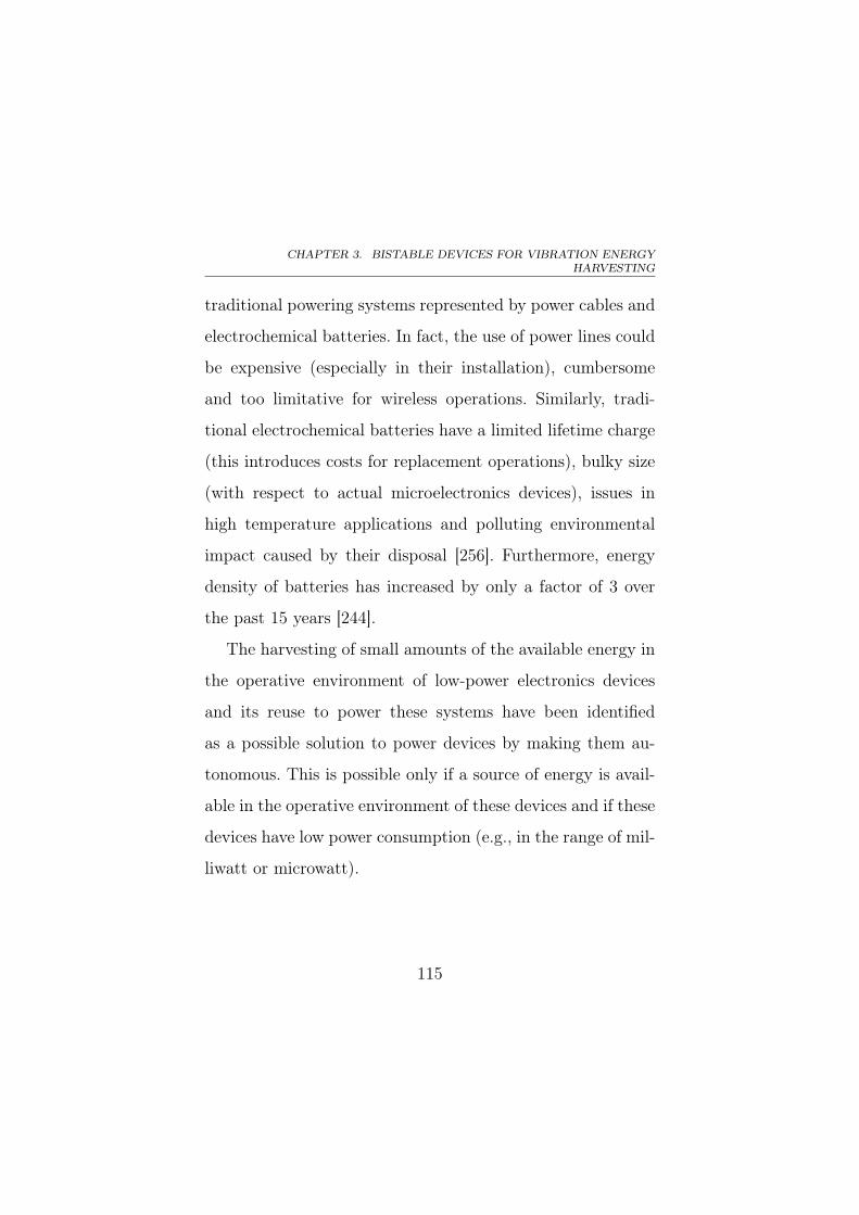
CHAPTER 3. BISTABLE DEVICES FOR VIBRATION ENERGYHARVESTING
traditional powering systems represented by power cables and
electrochemical batteries. In fact, the use of power lines could
be expensive (especially in their installation), cumbersome
and too limitative for wireless operations. Similarly, tradi-
tional electrochemical batteries have a limited lifetime charge
(this introduces costs for replacement operations), bulky size
(with respect to actual microelectronics devices), issues in
high temperature applications and polluting environmental
impact caused by their disposal [256]. Furthermore, energy
density of batteries has increased by only a factor of 3 over
the past 15 years [244].
The harvesting of small amounts of the available energy in
the operative environment of low-power electronics devices
and its reuse to power these systems have been identified
as a possible solution to power devices by making them au-
tonomous. This is possible only if a source of energy is avail-
able in the operative environment of these devices and if these
devices have low power consumption (e.g., in the range of mil-
liwatt or microwatt).
115
3.1. ENERGY HARVESTING FROM VIBRATIONS: STATE OF THE ART
Some data about power consumption of several target de-
vices for energy harvesting applications are shown in the plot
in fig. 3.1, as reported in literature [108].
Fig. 3.1 – Plot of the power consumption of several target devices for en-
ergy harvesting applications compared with power available from batteries
and power scavenged by energy harvesters in actual technologies [108].
A very recurrent example of application of energy harvest-
ing in literature is given by wireless sensor networks, which
116
CHAPTER 3. BISTABLE DEVICES FOR VIBRATION ENERGYHARVESTING
are commonly used in several monitoring and control appli-
cations like environmental and structural monitoring, smart
cities, medical remote sensing, military and aerospace appli-
cations and so on [202]. Each node of the network is usually
composed of one or more sensors, a microcontroller unit and a
transceiver with antenna for wireless communication (which is
the most power consuming component of the node, especially
during transmission and receiving activities). The power con-
sumption of a sensor node has been estimated between 1 μW
and 2 μW by various authors in recent works [244]. Tradi-
tionally, the power of each node is provided by electrochem-
ical batteries having often large size and a limited lifetime
(typically between one and ten years). When the charge in
these batteries is low, as already said, the need of substitut-
ing them introduces maintenance costs and issues if the num-
ber of nodes is high and harsh environments are involved.
Sometimes lifetime of nodes ends when batteries must be re-
placed because of costs. If miniaturized energy harvesters are
adopted, each sensor node become autonomous and its life-
time is indefinitely extended. Furthermore, the development
117
3.1. ENERGY HARVESTING FROM VIBRATIONS: STATE OF THE ART
of fabrication technologies at microscale (e.g., MEMS) results
in the possibility to reduce the size of nodes [256]. This also
increase the range of potential applications, opening the pos-
sibility to create ubiquitous wireless sensor networks.
A brief survey of available sources of energy is presented
in subsection 3.1.1.
3.1.1 Sources of energy
Several forms of energy sources have been considered for
energy harvesting applications, along with their transduction
mechanisms to proper generate an electrical output [244]. Op-
tical energy usually consists in sunlight that exploits photo-
voltaic effects [181]. Kinetic energy is generally represented by
mechanical vibrations [202], whose mechanical energy can be
converted by means of piezoelectric [81], electrostatic [162],
electromagnetic [47] and magnetostrictive [245] transducers.
Thermal energy is given by thermal gradients transduced
through thermoelectric effects such as Seebeck effects [144].
RF energy is captured through antennas and converted through
electromagnetic transduction [118]. Chemical energy is used
in energy harvesting applications through fuel cells [125].
118
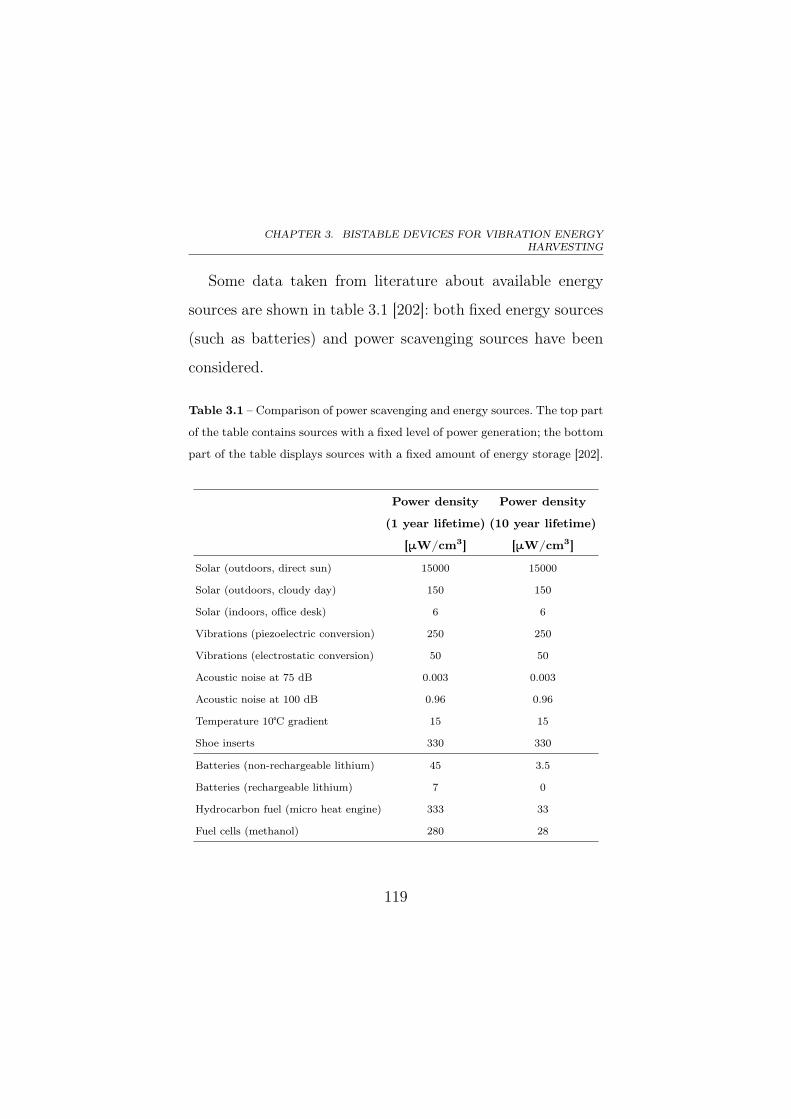
CHAPTER 3. BISTABLE DEVICES FOR VIBRATION ENERGYHARVESTING
Some data taken from literature about available energy
sources are shown in table 3.1 [202]: both fixed energy sources
(such as batteries) and power scavenging sources have been
considered.
Table 3.1 – Comparison of power scavenging and energy sources. The top part
of the table contains sources with a fixed level of power generation; the bottom
part of the table displays sources with a fixed amount of energy storage [202].
Power density Power density
(1 year lifetime) (10 year lifetime)
[μW/cm3] [μW/cm3]
Solar (outdoors, direct sun) 15000 15000
Solar (outdoors, cloudy day) 150 150
Solar (indoors, office desk) 6 6
Vibrations (piezoelectric conversion) 250 250
Vibrations (electrostatic conversion) 50 50
Acoustic noise at 75 dB 0.003 0.003
Acoustic noise at 100 dB 0.96 0.96
Temperature 10℃ gradient 15 15
Shoe inserts 330 330
Batteries (non-rechargeable lithium) 45 3.5
Batteries (rechargeable lithium) 7 0
Hydrocarbon fuel (micro heat engine) 333 33
Fuel cells (methanol) 280 28
119
3.1. ENERGY HARVESTING FROM VIBRATIONS: STATE OF THE ART
The data show that batteries are a reasonable solution only
for short lifetimes. However, another solution is requested for
long lifetimes. Fuel cells represent a potentially large improve-
ment over batteries as an energy reservoir but research to
miniaturize fuel cells is currently underway, even if it is very
promising [262]. Solar cells offer excellent power density only
in direct sunlight. However, in dim office lighting, or areas
with no light, they are inadequate. Power scavenged from ther-
mal gradients is also substantial enough to be of interest if the
necessary thermal gradients are available. It is, however, diffi-
cult to find thermal gradients greater than a 10℃ in a volume
of 1 cm3.
Among different power sources, mechanical vibrations rep-
resent one of the most ubiquitously and continuously available
sources that can potentially deliver a significant amount of en-
ergy. For this reason, kinetic energy from vibrational sources
has been watched with an increasing interest by scientific com-
munity in order to build generators able to efficiently scavenge
energy to power low-power mobile electronic devices.
120
CHAPTER 3. BISTABLE DEVICES FOR VIBRATION ENERGYHARVESTING
A more detailed overview about vibrational energy sources
is reported in subsection 3.1.2 and some details about energy
harvesters from mechanical vibrations are discussed in sub-
section 3.1.3.
3.1.2 Sources of mechanical vibrations
Vibration is a mechanical phenomenon whereby oscilla-
tions occur around an equilibrium point. They are two kinds of
mechanical vibrations: free vibrations and forced vibrations.
Free vibrations are generated by mechanical vibrating sys-
tems without any external forcing; ideally, if those systems
are non subjected to any kind of friction, damping or energy
loss, they would continue to vibrate for an infinite time; such
systems vibrate because they are forced by their non-zero ini-
tial conditions; a simple example is the case of an inertial
mass connected to a frame by means of a spring initially com-
pressed. Forced vibrations occur when an external forcing is
applied to the system, for example in a washing machine,
whose drum, equipped with a shock absorber, is continuously
subjected to a rotating force and to an inertial force generated
by the asymmetrical arrangement of inside clothes [194].
121
3.1. ENERGY HARVESTING FROM VIBRATIONS: STATE OF THE ART
Ambient mechanical vibrations (also known as ambient
noisy vibrations) come in a large variety of forms such as
induced oscillations, seismic noise, vehicle motion, acoustic
noise, multitone vibrating systems, and, more generally, noisy
environments. Suitable vibrations can be found in numer-
ous applications including common household goods (fridges,
washing machines, microwave ovens etc), industrial plant
equipments, moving structures such as automobiles and aero-
planes and structures such as buildings and bridges [17].
Depending on the mechanism that generates vibrations,
existing vibrational sources can be categorized into three ma-
jor groups [189]. The first group is composed of rigid struc-
tures subjected to their own movement such as vehicles in
general, containers, mobile devices, fans and motors, eleva-
tors and escalators in public places, home appliances, refrig-
erators, bridges, building structures and so on. The second
group consists of elastic structures exhibiting an elastic defor-
mation of their walls such as rotor blades, wings of airplanes,
pumps, motors, pipelines, ventilation and air conditioning. Fi-
nally, the third group is given by compliant structures with
122
CHAPTER 3. BISTABLE DEVICES FOR VIBRATION ENERGYHARVESTING
low modulus of elasticity and high deformation coefficients
like textile materials, leather, rubber tubing, pipelines typi-
cally traveled by a moving fluid, etc.
Vibrations sources are typically considered as accelera-
tions characterized in terms of acceleration magnitude and
frequency spectrum with an associated kinetic energy [194].
On the basis of the acceleration magnitude, vibrations are
generally classified into: low-magnitude vibrations (if ampli-
tude is lower than 0.1 m/s2), mid-magnitude vibrations (when
amplitude is between 0.1 m/s2 an 2 m/s2) and high-magnitude
vibrations (if amplitude is larger than 2 m/s2) [194].
On the basis of the frequency spectrum of the source, vi-
brations can be categorized into: wideband vibrations (if a
bandwidth larger than about 100 Hz is exhibited) and reso-
nant or quite-resonant vibrations (if they are characterized by
narrow energy spectra with a few peaked modes). In the case
of resonant or quite-resonant vibrations, it is possible to dis-
tinguish low-frequency vibrations (if main harmonics are con-
fined in a range below 10 Hz), mid-frequency vibrations (when
main harmonics are contained in a range between 10 Hz and
123
3.1. ENERGY HARVESTING FROM VIBRATIONS: STATE OF THE ART
150 Hz) and high-frequency vibrations (if main harmonics are
within a range starting over 150 Hz) [189].
In terms of the level of the kinetic energy carried by vibra-
tions, it is possible to split vibrations into two groups. First
group is given by low-level vibrations that convey a low or
a mid level of energy; this sort of source can be found in a
very wide range of applications, especially in domestic and
civil fields. Second group is represented by high-level vibra-
tions, coming from industrial applications, having a potential
smaller range of applications than low-level vibrations [27].
For example, human based sources are generally character-
ized by low frequency high amplitude accelerations, as shown
in the time series of the acceleration of the footsteps of a walk-
ing and a running person reported respectively in fig. 3.2 and
in fig. 3.3.
The kinetic energy carried by vibration sources is strongly
committed with magnitude and spectrum of the associated
accelerations. In fact, sometimes, the delivered energy is con-
centrated in a very tight region of the frequency spectrum, as
in the case of rotating machines [263], especially when oscil-
124
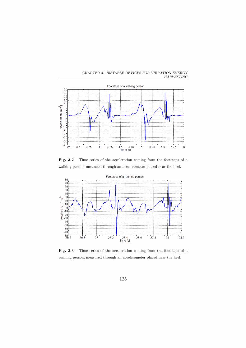
CHAPTER 3. BISTABLE DEVICES FOR VIBRATION ENERGYHARVESTING
Fig. 3.2 – Time series of the acceleration coming from the footsteps of a
walking person, measured through an accelerometer placed near the heel.
Fig. 3.3 – Time series of the acceleration coming from the footsteps of a
running person, measured through an accelerometer placed near the heel.
125
3.1. ENERGY HARVESTING FROM VIBRATIONS: STATE OF THE ART
lations from vibrations follow a periodic or defined dynamics.
On the contrary, energy is very often distributed over a wide
spectrum of frequencies in other applications; in particular,
several scenarios exist where a significant fraction of energy is
generally distributed in the lower part of the frequency spec-
trum, below 500 Hz [200]: this is the case of vibrations having
random dynamics.
Some data on mechanical sources of low-level vibrations
are listed in table 3.2, as reported from literature [202].
Two examples of vibration spectra (a small microwave oven
and a large office windows next to a busy street), taken from
literature [202], are illustrated in fig. 3.4.
In order to harvest energy from mechanical vibrations, the
first step is to study and characterize the specifications of the
vibrational target source and then trying to find a solution
for the development of efficient energy harvesters. Several so-
lutions matching with different sources exist. The strategies
implemented in literature are presented in subsection 3.1.3,
along with some details about the architectures for vibration
126
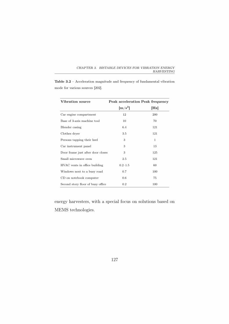
CHAPTER 3. BISTABLE DEVICES FOR VIBRATION ENERGYHARVESTING
Table 3.2 – Acceleration magnitude and frequency of fundamental vibration
mode for various sources [202].
Vibration source Peak acceleration Peak frequency
[m/s2] [Hz]
Car engine compartment 12 200
Base of 3-axis machine tool 10 70
Blender casing 6.4 121
Clothes dryer 3.5 121
Persons tapping their heel 3 1
Car instrument panel 3 13
Door frame just after door closes 3 125
Small microwave oven 2.5 121
HVAC vents in office building 0.2–1.5 60
Windows next to a busy road 0.7 100
CD on notebook computer 0.6 75
Second story floor of busy office 0.2 100
energy harvesters, with a special focus on solutions based on
MEMS technologies.
127
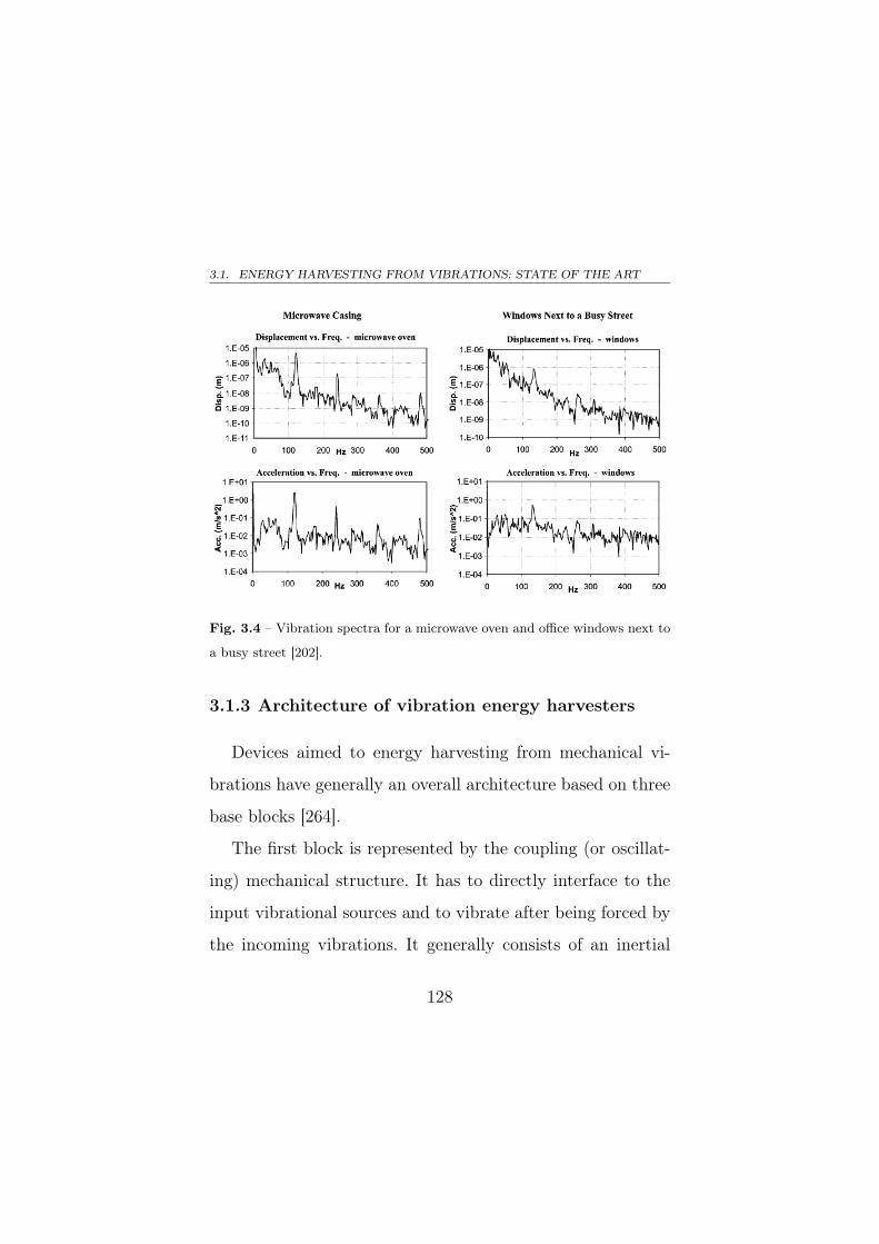
3.1. ENERGY HARVESTING FROM VIBRATIONS: STATE OF THE ART
Fig. 3.4 – Vibration spectra for a microwave oven and office windows next to
a busy street [202].
3.1.3 Architecture of vibration energy harvesters
Devices aimed to energy harvesting from mechanical vi-
brations have generally an overall architecture based on three
base blocks [264].
The first block is represented by the coupling (or oscillat-
ing) mechanical structure. It has to directly interface to the
input vibrational sources and to vibrate after being forced by
the incoming vibrations. It generally consists of an inertial
128
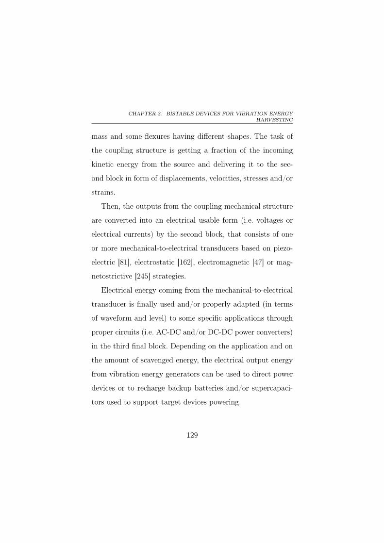
CHAPTER 3. BISTABLE DEVICES FOR VIBRATION ENERGYHARVESTING
mass and some flexures having different shapes. The task of
the coupling structure is getting a fraction of the incoming
kinetic energy from the source and delivering it to the sec-
ond block in form of displacements, velocities, stresses and/or
strains.
Then, the outputs from the coupling mechanical structure
are converted into an electrical usable form (i.e. voltages or
electrical currents) by the second block, that consists of one
or more mechanical-to-electrical transducers based on piezo-
electric [81], electrostatic [162], electromagnetic [47] or mag-
netostrictive [245] strategies.
Electrical energy coming from the mechanical-to-electrical
transducer is finally used and/or properly adapted (in terms
of waveform and level) to some specific applications through
proper circuits (i.e. AC-DC and/or DC-DC power converters)
in the third final block. Depending on the application and on
the amount of scavenged energy, the electrical output energy
from vibration energy generators can be used to direct power
devices or to recharge backup batteries and/or supercapaci-
tors used to support target devices powering.
129
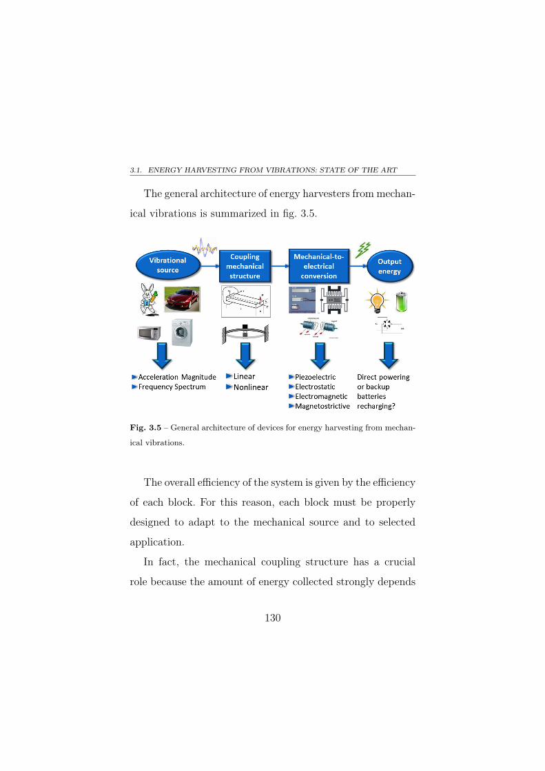
3.1. ENERGY HARVESTING FROM VIBRATIONS: STATE OF THE ART
The general architecture of energy harvesters from mechan-
ical vibrations is summarized in fig. 3.5.
Fig. 3.5 – General architecture of devices for energy harvesting from mechan-
ical vibrations.
The overall efficiency of the system is given by the efficiency
of each block. For this reason, each block must be properly
designed to adapt to the mechanical source and to selected
application.
In fact, the mechanical coupling structure has a crucial
role because the amount of energy collected strongly depends
130
CHAPTER 3. BISTABLE DEVICES FOR VIBRATION ENERGYHARVESTING
on it and consequently it affects heavily the efficiency of the
overall system. Its definition cannot be separated, upstream,
by the characteristics of the source and, downstream, by the
transducer specifications. Depending on the application, sev-
eral types of structures have been proposed and studied in the
literature and, because of the aim of this work, they will be
illustrated in subsections 3.1.4, 3.1.5 and 3.1.6.
In the same way of coupling structures, mechanical-to-
electrical transducers have a huge impact on the harvester
efficiency, but, due to the topic of this work, they will be gen-
erally discussed in subsection 3.1.7.
3.1.4 Linear resonant coupling structures
Traditionally mechanical coupling structures have been
based on linear resonant structures, which are characterized
by a linear relationship between displacement and reaction
forces.
An example of linear resonant structure is represented by a
cantilever beam having a proof mass on its free end and expe-
riencing linear elastic deformations. In this case, accelerations
coming from the vibrational sources put in oscillation the can-
131
3.1. ENERGY HARVESTING FROM VIBRATIONS: STATE OF THE ART
tilever beam (especially its free end) by means of the proof
mass. Beam oscillations are then converted both in stresses
and strains, near the fixed end of the beam (attached to a
fixed inertial frame), and in displacements and velocities in
the “moving” free end of the beam.
The dynamics of this kind of structures is typically modeled
through the 1 degree-of-freedom second-order mass-damper-
stiffness model in (3.1) [223].
mz + cmz + ce(z, z) + kz = −my (3.1)
where m is the proof mass, k is the stiffness coefficient
of the beam, cm is the coefficient of mechanical damping ce
is the damping of the mechanical-to-electrical transducer, y is
the absolute external acceleration applied to the inertial frame
and z, z and z are respectively the relative (with respect to
the inertial frame) displacement, velocity and acceleration of
the free end of the cantilever beam.
The modeling of the mass-damper-stiffness system is illus-
trated in fig 3.6, along with a schematization of a cantilever
beam with proof mass.
132
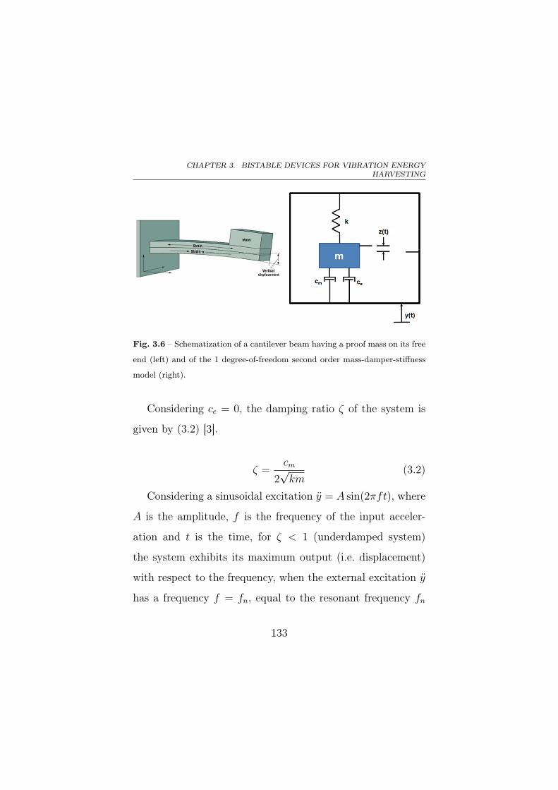
CHAPTER 3. BISTABLE DEVICES FOR VIBRATION ENERGYHARVESTING
Fig. 3.6 – Schematization of a cantilever beam having a proof mass on its free
end (left) and of the 1 degree-of-freedom second order mass-damper-stiffness
model (right).
Considering ce = 0, the damping ratio ζ of the system is
given by (3.2) [3].
ζ =cm
2√km
(3.2)
Considering a sinusoidal excitation y = A sin(2πft), where
A is the amplitude, f is the frequency of the input acceler-
ation and t is the time, for ζ < 1 (underdamped system)
the system exhibits its maximum output (i.e. displacement)
with respect to the frequency, when the external excitation y
has a frequency f = fn, equal to the resonant frequency fn
133
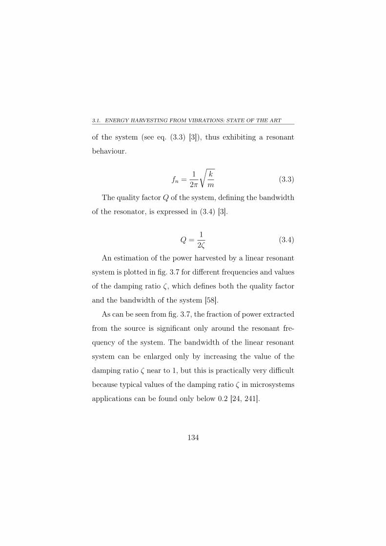
3.1. ENERGY HARVESTING FROM VIBRATIONS: STATE OF THE ART
of the system (see eq. (3.3) [3]), thus exhibiting a resonant
behaviour.
fn =1
2π
√k
m(3.3)
The quality factor Q of the system, defining the bandwidth
of the resonator, is expressed in (3.4) [3].
Q =1
2ζ(3.4)
An estimation of the power harvested by a linear resonant
system is plotted in fig. 3.7 for different frequencies and values
of the damping ratio ζ, which defines both the quality factor
and the bandwidth of the system [58].
As can be seen from fig. 3.7, the fraction of power extracted
from the source is significant only around the resonant fre-
quency of the system. The bandwidth of the linear resonant
system can be enlarged only by increasing the value of the
damping ratio ζ near to 1, but this is practically very difficult
because typical values of the damping ratio ζ in microsystems
applications can be found only below 0.2 [24, 241].
134
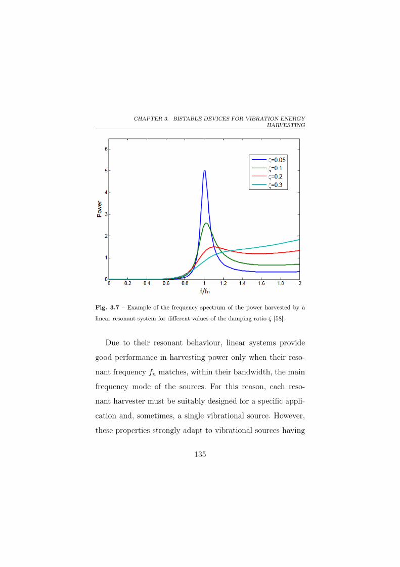
CHAPTER 3. BISTABLE DEVICES FOR VIBRATION ENERGYHARVESTING
Fig. 3.7 – Example of the frequency spectrum of the power harvested by a
linear resonant system for different values of the damping ratio ζ [58].
Due to their resonant behaviour, linear systems provide
good performance in harvesting power only when their reso-
nant frequency fn matches, within their bandwidth, the main
frequency mode of the sources. For this reason, each reso-
nant harvester must be suitably designed for a specific appli-
cation and, sometimes, a single vibrational source. However,
these properties strongly adapt to vibrational sources having
135
3.1. ENERGY HARVESTING FROM VIBRATIONS: STATE OF THE ART
a narrow spectrum and one peaked resonant mode but lead
linear systems to poor performance outside their resonant fre-
quencies and impose several constraints and limitations to the
design and fabrication (especially in MEMS technologies) of
these systems.
In fact, MEMS resonators can be very sensitive to small
dimensional imperfections caused by microfabrication pro-
cesses and this results in disadvantageous fluctuations in ef-
ficiency, because frequency matching is inaccurate. Moreover,
the achievement of very low resonance frequencies (e.g., in the
order of a few hundreds of hertz or lower) with a significantly
large quality factor is a challenging issue at microscale, and
therefore, resonant microsystems will generally work outside
resonance and thus have a poor efficiency. A further reduction
is experienced in the case of wideband vibrations since linear
resonant devices collect energy mainly around their resonance
peak [161].
For these reasons, the necessity of enlarging the bandwidth
of energy harvesting devices, of overcoming the need of fre-
quency matching with the source and of allowing for the down-
136
CHAPTER 3. BISTABLE DEVICES FOR VIBRATION ENERGYHARVESTING
scaling of devices without loosing too much efficiency have
pushed scientific research to find novel solutions for energy
harvesters [232, 269].
Those solutions will be presented in subsection 3.1.5.
3.1.5 Coupling mechanical structures: from linear to
nonlinear
Several solutions have been proposed to overcome the lim-
its of linear resonant devices and to improve their perfor-
mance, especially at microscale, where the power per volume
unit scavenged by microgenerators is quite low. In particu-
lar, two different approaches have been followed by research.
The first one deals with the development of systems having
the ability to adjust or tune (autonomously or through a con-
trol strategy) their resonant frequency so that it can match
the main mode of the vibrational sources at all time and sit-
uations. The second path is aimed to enlarge the operative
bandwidth of harvesters by involving either linear or nonlin-
ear strategies [269].
The adjustment of resonant frequencies in linear harvesters
is performed by changing the mechanical characteristics of the
137
3.1. ENERGY HARVESTING FROM VIBRATIONS: STATE OF THE ART
structure or the electrical load of the generator. Changing the
mechanical characteristics of a generator has previously been
called passive or active tuning depending on the approach.
Passive tuning is defined as a tuning mechanism that op-
erates periodically. This approach consists in tuning the gen-
erator before its operation and afterwards in turning off the
tuning system while the new resonance frequency is main-
tained during harvesting operation. This strategy only con-
sumes power during the tuning operation and uses negligible
energy once the generator is matched to the frequency of the
ambient vibrations.
Active tuning is defined as a tuning mechanism that runs
continuously for matching and eventually adjusting the res-
onant frequency of the mechanical oscillating structure with
the ambient vibration frequency.
Since both of these approaches involve some form of ac-
tive process, the tuning process is power consuming, so the
first constraint is to scavenge a larger amount of power from
the source than the power spent in adjusting the harvester
characteristics [204].
138
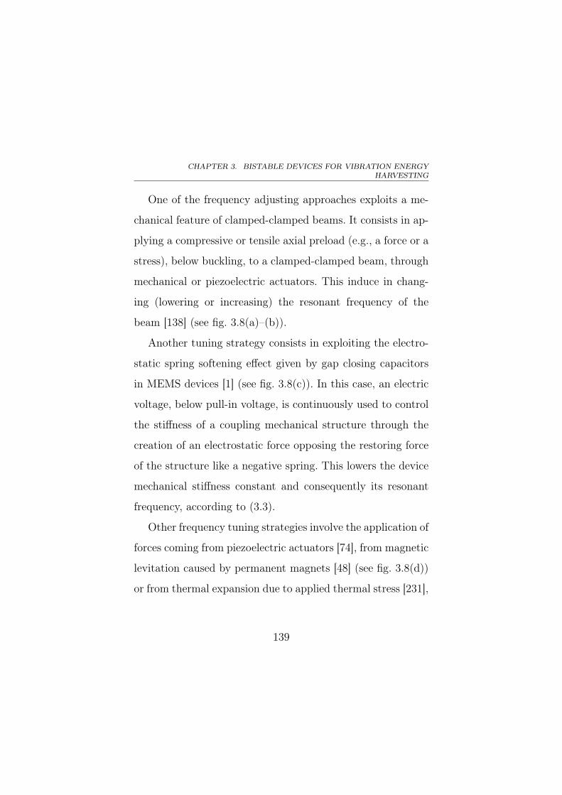
CHAPTER 3. BISTABLE DEVICES FOR VIBRATION ENERGYHARVESTING
One of the frequency adjusting approaches exploits a me-
chanical feature of clamped-clamped beams. It consists in ap-
plying a compressive or tensile axial preload (e.g., a force or a
stress), below buckling, to a clamped-clamped beam, through
mechanical or piezoelectric actuators. This induce in chang-
ing (lowering or increasing) the resonant frequency of the
beam [138] (see fig. 3.8(a)–(b)).
Another tuning strategy consists in exploiting the electro-
static spring softening effect given by gap closing capacitors
in MEMS devices [1] (see fig. 3.8(c)). In this case, an electric
voltage, below pull-in voltage, is continuously used to control
the stiffness of a coupling mechanical structure through the
creation of an electrostatic force opposing the restoring force
of the structure like a negative spring. This lowers the device
mechanical stiffness constant and consequently its resonant
frequency, according to (3.3).
Other frequency tuning strategies involve the application of
forces coming from piezoelectric actuators [74], from magnetic
levitation caused by permanent magnets [48] (see fig. 3.8(d))
or from thermal expansion due to applied thermal stress [231],
139
3.1. ENERGY HARVESTING FROM VIBRATIONS: STATE OF THE ART
in order to affect the mechanical properties of the oscillating
structure.
Fig. 3.8 – (a) Resonant frequency tuning of a clamped-clamped beam through
axial preload [138]. (b) Resonant frequency shift after tensile and compressive
axial preload of clamped-clamped beam [138]. (c) Example of structure exploit-
ing electrostatic spring softening to tune resonant frequency [1]. (d) Resonant
frequency tuning through magnetic levitation forces [48].
A different way in tuning the resonant frequency of de-
vices is exploiting an electrical tuning to change the electri-
140
CHAPTER 3. BISTABLE DEVICES FOR VIBRATION ENERGYHARVESTING
cal damping ce in (3.1) by adjusting the load, which causes
the power spectrum of the generator to shift. This strategy
has been applied to energy harvesters having piezoelectric
mechanical-to-electrical transducers. As resistive loads reduce
the efficiency of power transfer and load inductances are diffi-
cult to be varied, it is most feasible to adjust capacitive loads
to realize electrical tuning [258].
The second approach is to widen the bandwidth (i.e. the
operative frequency range) of the generator in order to in-
crease the device performance and make it compatible with
several vibrational source, without tuning needs.
The first method consists in a generator composed of an
array (named “mechanical band-pass filter”) of small linear
resonant generators (i.e. cantilever beams), each of which has
different dimensions and mass and hence different resonant
frequencies, as in fig. 3.9(a). Considering the superimposition
of the frequency spectra of these devices (e.g., when these
devices are connected in series), the operative bandwidth is
widened, whilst the quality factor does not decrease and larger
dimensions are required [214] (see fig. 3.9(b)).
141
3.1. ENERGY HARVESTING FROM VIBRATIONS: STATE OF THE ART
Another strategy is given by multi-mass systems, where
several proof masses having different dimensions are placed in
appropriate positions on a clamped-clamped beam [201].
The adoption of amplitude limiters (e.g., mechanical stop-
pers) in order to limits the oscillation magnitude in mi-
croresonators (i.e. cantilever beams) has been proven as an-
other strategy to improve microgenerators performance (see
fig. 3.9(c)). In this case, some kinds of nonlinearities intro-
duced by the impacts between the mechanical stopper and
the oscillating structure (see fig. 3.9(d)) positively affect de-
vice dynamics and enlarge device bandwidth [145].
A novel identified approach to widen the bandwidth of mi-
crogenerators is to exploit the nonlinear dynamics descend-
ing from certain structures. In this case, nonlinearities arise
from the adoption of structures having defined shapes or ex-
ploiting the interaction of components coming from different
physics fields (like mechanical structures and permanent mag-
nets) [60].
142
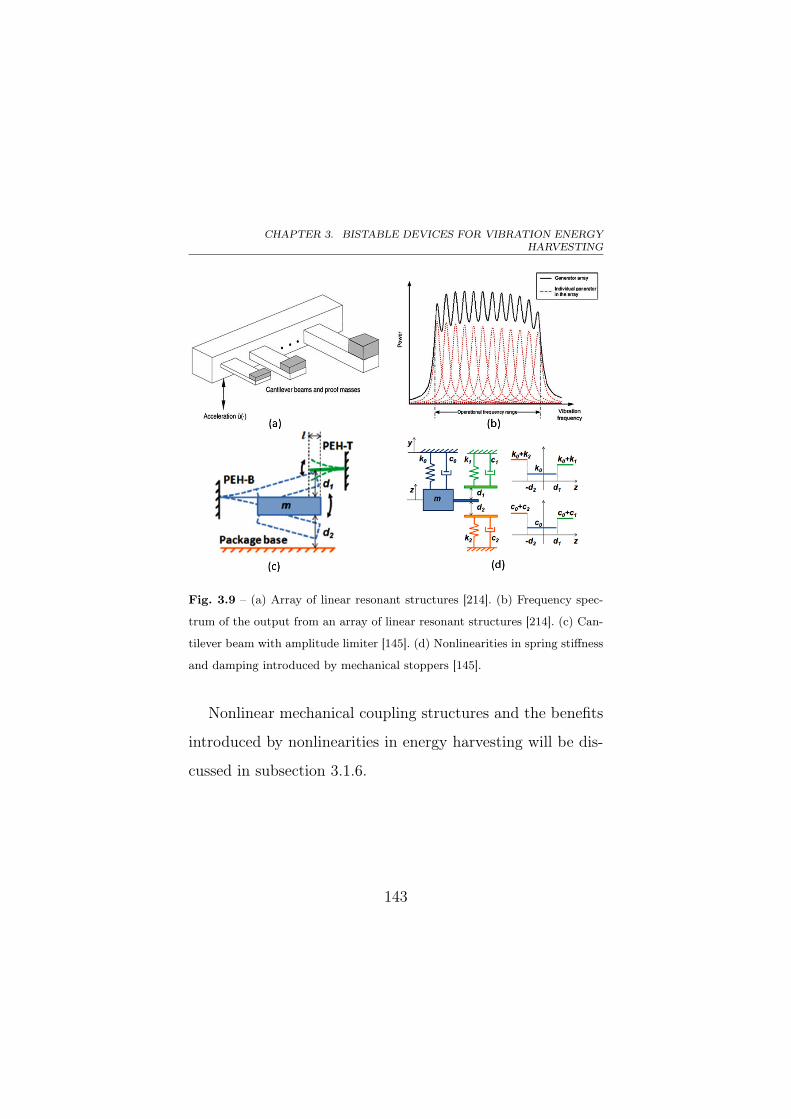
CHAPTER 3. BISTABLE DEVICES FOR VIBRATION ENERGYHARVESTING
Fig. 3.9 – (a) Array of linear resonant structures [214]. (b) Frequency spec-
trum of the output from an array of linear resonant structures [214]. (c) Can-
tilever beam with amplitude limiter [145]. (d) Nonlinearities in spring stiffness
and damping introduced by mechanical stoppers [145].
Nonlinear mechanical coupling structures and the benefits
introduced by nonlinearities in energy harvesting will be dis-
cussed in subsection 3.1.6.
143
3.1. ENERGY HARVESTING FROM VIBRATIONS: STATE OF THE ART
3.1.6 Nonlinear coupling structures
Nonlinear mechanical coupling structures have been pro-
posed to overcome the limits of linear resonant structures and
of tuning systems by increasing the complexity of the harvest-
ing systems.
Several mechanisms have been explored to induce nonlin-
earity in a coupling mechanical structure. One strategy ex-
ploits the adoption of nonlinear elastic springs where non-
linearity is introduced by the geometrical parameters of the
structure and/or by the properties of the materials used in
the device [17]. Another strategy applies stresses/strains in
mechanical structures to implement nonlinear behaviour, as
an example in buckled beams [59]. Another approach couples
mechanics with other fields (e.g., magnetics) to allow for non-
linearities [9].
In the case of mechanical nonlinearities, the second-order
mass-damper-stiffness model in (3.1) modifies in (3.5) [60].
mz + cmz + ce(z, z) + k(z) = −my (3.5)
144
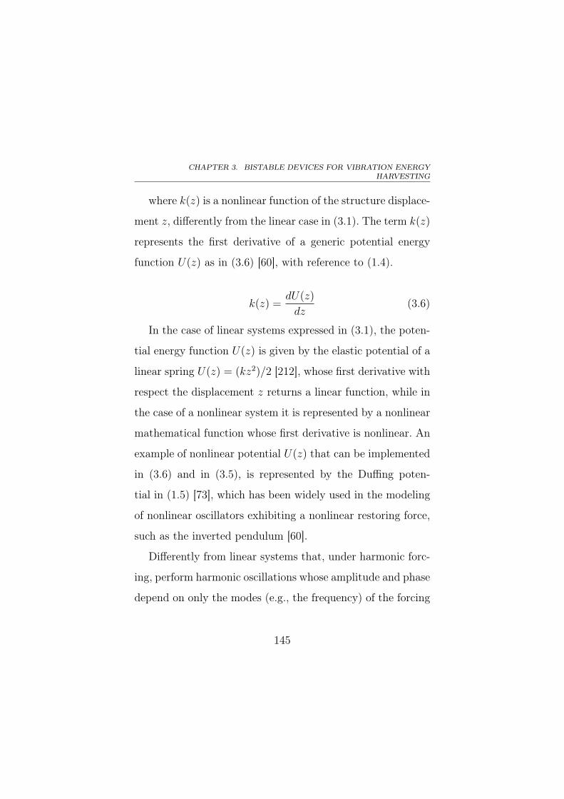
CHAPTER 3. BISTABLE DEVICES FOR VIBRATION ENERGYHARVESTING
where k(z) is a nonlinear function of the structure displace-
ment z, differently from the linear case in (3.1). The term k(z)
represents the first derivative of a generic potential energy
function U(z) as in (3.6) [60], with reference to (1.4).
k(z) =dU(z)
dz(3.6)
In the case of linear systems expressed in (3.1), the poten-
tial energy function U(z) is given by the elastic potential of a
linear spring U(z) = (kz2)/2 [212], whose first derivative with
respect the displacement z returns a linear function, while in
the case of a nonlinear system it is represented by a nonlinear
mathematical function whose first derivative is nonlinear. An
example of nonlinear potential U(z) that can be implemented
in (3.6) and in (3.5), is represented by the Duffing poten-
tial in (1.5) [73], which has been widely used in the modeling
of nonlinear oscillators exhibiting a nonlinear restoring force,
such as the inverted pendulum [60].
Differently from linear systems that, under harmonic forc-
ing, perform harmonic oscillations whose amplitude and phase
depend on only the modes (e.g., the frequency) of the forcing
145
3.1. ENERGY HARVESTING FROM VIBRATIONS: STATE OF THE ART
input, the behaviour of nonlinear systems is characterized, un-
der harmonic forcing, by nonlinear nonharmonic oscillations,
whose amplitude and phase depend on both the amplitude
and the modes of the input forcing [101].
As an example, in the case of Duffing oscillator, the fre-
quency response of the system in terms of amplitude A and
phase φ can lead to different behaviours for increasing and
decreasing values of the input forcing for different values of
the parameter a from (1.5), as shown in fig. 3.10 [113].
In the case of nonlinear oscillating systems, resonant be-
haviours can be found and are known as nonlinear resonance
because they are determined by both the amplitude and the
frequency of the input forcing, differently from linear reso-
nance.
The dependency of the eigenfrequency of a nonlinear os-
cillator on the amplitude and the nonharmoniticity of the os-
cillation lead to behaviours that are impossible in harmonic
oscillators, namely, the foldover effect and superharmonic res-
onance, respectively [76].
146
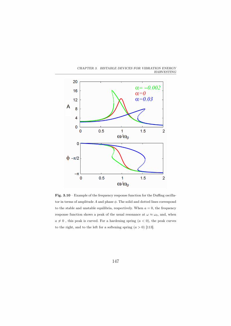
CHAPTER 3. BISTABLE DEVICES FOR VIBRATION ENERGYHARVESTING
Fig. 3.10 – Example of the frequency response function for the Duffing oscilla-
tor in terms of amplitude A and phase φ. The solid and dotted lines correspond
to the stable and unstable equilibria, respectively. When a = 0, the frequency
response function shows a peak of the usual resonance at ω ≈ ω0, and, when
a �= 0 , this peak is curved. For a hardening spring (a < 0), the peak curves
to the right, and to the left for a softening spring (a > 0) [113].
147
3.1. ENERGY HARVESTING FROM VIBRATIONS: STATE OF THE ART
The foldover effect gets its name from the bending of the
resonance peak in a amplitude versus frequency plot. This
bending is due to the frequency-amplitude relation which is
typical for nonlinear oscillators. As an example, the frequency
response of a sinusoidally driven inverted pendulum is shown
in fig. 3.11. As long as the driving amplitude A is “small”, the
resonance line is very well approximated by the result for an
underdamped harmonic oscillator. For a stronger driving, the
resonance lines “folds”, leading to bistability and hysteresis.
That is, the nonlinear oscillator oscillates either with a large
amplitude or a small amplitude. In the middle there is always
an unstable periodic solution (shown as a dotted line). At
the ends of the interval of bistability, this unstable limit cycle
annihilates with one of its stable counterpart in a saddle-node
bifurcation [77].
The foldover effect also occurs in superharmonic resonance.
Because nonlinear oscillators do not oscillate harmonically,
their oscillation is a (infinite) sum of harmonic (i.e., sinu-
soidal) oscillations with frequencies which are integer mul-
tiples of the fundamental frequency (i.e the inverse of the pe-
148
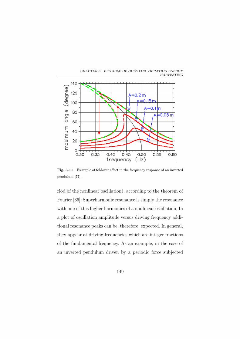
CHAPTER 3. BISTABLE DEVICES FOR VIBRATION ENERGYHARVESTING
Fig. 3.11 – Example of foldover effect in the frequency response of an inverted
pendulum [77].
riod of the nonlinear oscillation), according to the theorem of
Fourier [36]. Superharmonic resonance is simply the resonance
with one of this higher harmonics of a nonlinear oscillation. In
a plot of oscillation amplitude versus driving frequency addi-
tional resonance peaks can be, therefore, expected. In general,
they appear at driving frequencies which are integer fractions
of the fundamental frequency. As an example, in the case of
an inverted pendulum driven by a periodic force subjected
149
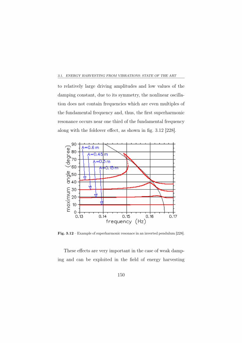
3.1. ENERGY HARVESTING FROM VIBRATIONS: STATE OF THE ART
to relatively large driving amplitudes and low values of the
damping constant, due to its symmetry, the nonlinear oscilla-
tion does not contain frequencies which are even multiples of
the fundamental frequency and, thus, the first superharmonic
resonance occurs near one third of the fundamental frequency
along with the foldover effect, as shown in fig. 3.12 [228].
Fig. 3.12 – Example of superharmonic resonace in an inverted pendulum [228].
These effects are very important in the case of weak damp-
ing and can be exploited in the field of energy harvesting
150
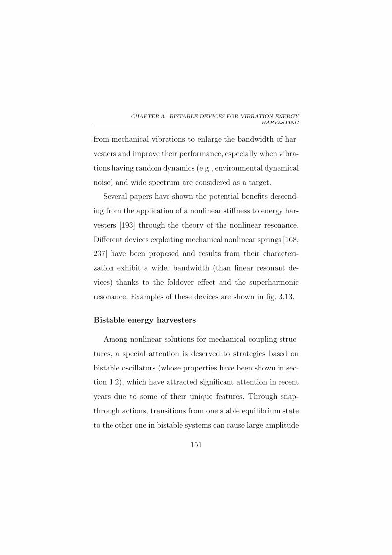
CHAPTER 3. BISTABLE DEVICES FOR VIBRATION ENERGYHARVESTING
from mechanical vibrations to enlarge the bandwidth of har-
vesters and improve their performance, especially when vibra-
tions having random dynamics (e.g., environmental dynamical
noise) and wide spectrum are considered as a target.
Several papers have shown the potential benefits descend-
ing from the application of a nonlinear stiffness to energy har-
vesters [193] through the theory of the nonlinear resonance.
Different devices exploiting mechanical nonlinear springs [168,
237] have been proposed and results from their characteri-
zation exhibit a wider bandwidth (than linear resonant de-
vices) thanks to the foldover effect and the superharmonic
resonance. Examples of these devices are shown in fig. 3.13.
Bistable energy harvesters
Among nonlinear solutions for mechanical coupling struc-
tures, a special attention is deserved to strategies based on
bistable oscillators (whose properties have been shown in sec-
tion 1.2), which have attracted significant attention in recent
years due to some of their unique features. Through snap-
through actions, transitions from one stable equilibrium state
to the other one in bistable systems can cause large amplitude
151
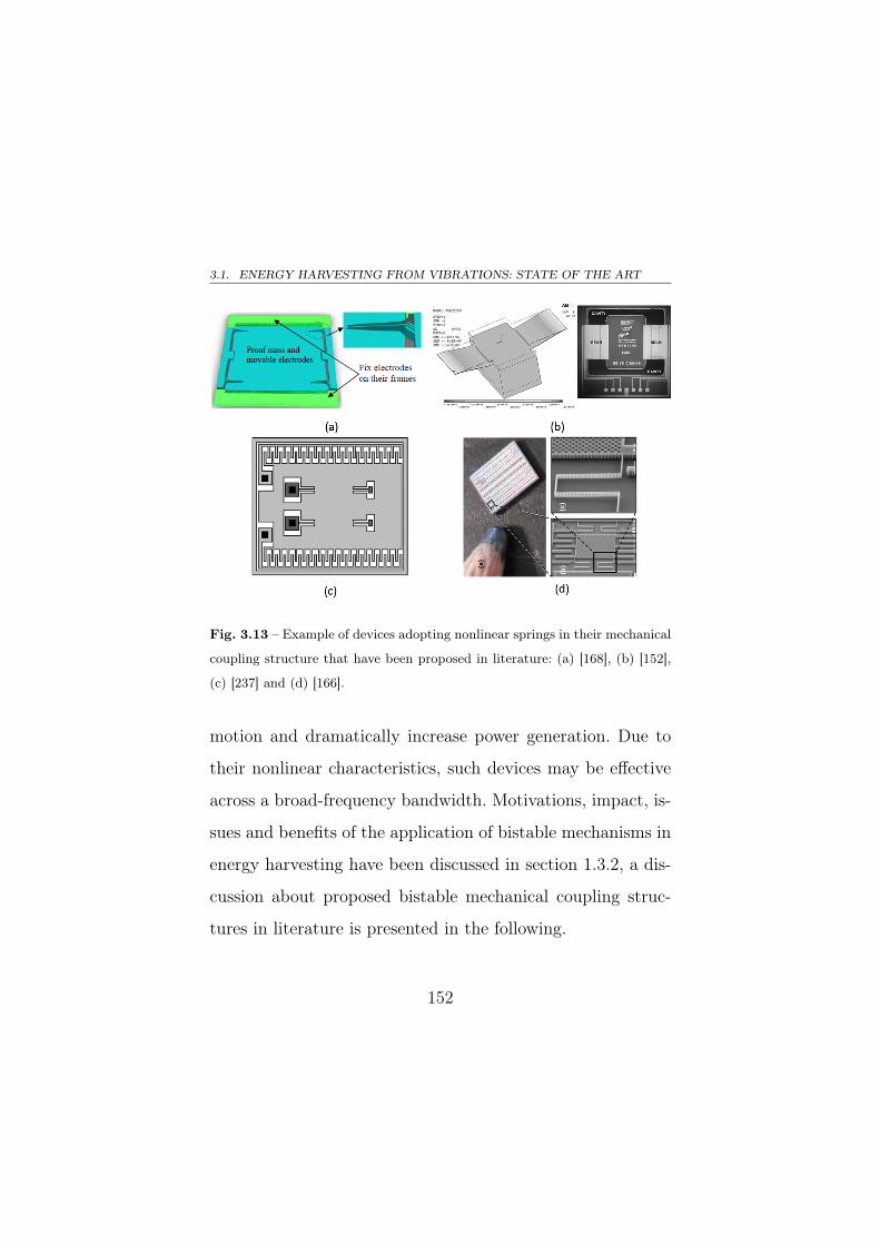
3.1. ENERGY HARVESTING FROM VIBRATIONS: STATE OF THE ART
Fig. 3.13 – Example of devices adopting nonlinear springs in their mechanical
coupling structure that have been proposed in literature: (a) [168], (b) [152],
(c) [237] and (d) [166].
motion and dramatically increase power generation. Due to
their nonlinear characteristics, such devices may be effective
across a broad-frequency bandwidth. Motivations, impact, is-
sues and benefits of the application of bistable mechanisms in
energy harvesting have been discussed in section 1.3.2, a dis-
cussion about proposed bistable mechanical coupling struc-
tures in literature is presented in the following.
152
CHAPTER 3. BISTABLE DEVICES FOR VIBRATION ENERGYHARVESTING
Bistable coupling mechanical structures proposed in the
literature can be categorized into three groups in terms of the
physical principle adopted to induce bistability.
The first group is composed of devices using magnetic at-
traction to allows for bistability in cantilevered ferromagnetic
beams as shown in fig. 3.14(a). In one of these configura-
tions, a centrally suspended magnet is attracted by two end-
suspended magnets along the axis of a tube. As base excita-
tion increases, the central magnet is attracted so as to mag-
netically attach to one of the end magnets; external excitation
thereafter causes the release of the central magnet from one
end, which allows the end magnet to ring down through the
axis of a coil, thus inducing flow of current in a harvesting
circuit [87].
The second group consists in devices exploiting magnetic
repulsion to destabilize the linear equilibrium position. Nu-
merous of these investigations have considered a cantilevered
piezoelectric beam with magnetic tip mass, having opposed
magnetization with respect to a facing fixed permanent mag-
net which may be moved a certain distance to the beam end
153
3.1. ENERGY HARVESTING FROM VIBRATIONS: STATE OF THE ART
so as to tailor the strength of the bistability and “tune” the
bistable potential, as illustrated in fig. 3.14(b). One feature
of this configuration is that the repulsive magnets may be
moved a great distance away so as to remove the nonlinearity
and provide for the comparison against an equivalent linear
harvester [83]. One of the drawbacks is due to the deposition
of permanent magnets on the tip of the cantilever beams that
is not so compatible with some MEMS technology batch pro-
cesses. Because the fabrication on MEMS devices of ferromag-
nets placed very close one each other and having non-parallel
magnetization is seriously challenging, solutions based on cou-
pled parallel cantilevers having an equally oriented permanent
magnet on each tip in order to provide repulsive forces that
in turn induce antisymmetric bistable behaviours in the can-
tilevers have been proposed [6] and adapted to multidimen-
sional applications [8].
The third group includes devices exploiting mechanical
properties, mechanical design and/or mechanical loading to
implement bistable coupling mechanical structures. Several
solutions are based on compliant mechanisms exhibiting bi-
154
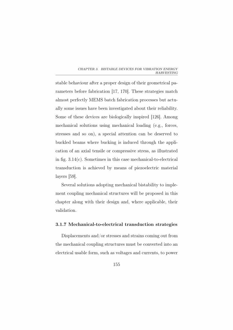
CHAPTER 3. BISTABLE DEVICES FOR VIBRATION ENERGYHARVESTING
stable behaviour after a proper design of their geometrical pa-
rameters before fabrication [17, 170]. These strategies match
almost perfectly MEMS batch fabrication processes but actu-
ally some issues have been investigated about their reliability.
Some of these devices are biologically inspired [126]. Among
mechanical solutions using mechanical loading (e.g., forces,
stresses and so on), a special attention can be deserved to
buckled beams where bucking is induced through the appli-
cation of an axial tensile or compressive stress, as illustrated
in fig. 3.14(c). Sometimes in this case mechanical-to-electrical
transduction is achieved by means of piezoelectric material
layers [59].
Several solutions adopting mechanical bistability to imple-
ment coupling mechanical structures will be proposed in this
chapter along with their design and, where applicable, their
validation.
3.1.7 Mechanical-to-electrical transduction strategies
Displacements and/or stresses and strains coming out from
the mechanical coupling structures must be converted into an
electrical usable form, such as voltages and currents, to power
155
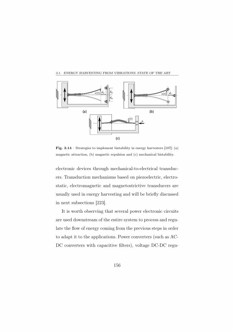
3.1. ENERGY HARVESTING FROM VIBRATIONS: STATE OF THE ART
Fig. 3.14 – Strategies to implement bistability in energy harvesters [107]: (a)
magnetic attraction, (b) magnetic repulsion and (c) mechanical bistability.
electronic devices through mechanical-to-electrical transduc-
ers. Transduction mechanisms based on piezoelectric, electro-
static, electromagnetic and magnetostrictive transducers are
usually used in energy harvesting and will be briefly discussed
in next subsections [223].
It is worth observing that several power electronic circuits
are used downstream of the entire system to process and regu-
late the flow of energy coming from the previous steps in order
to adapt it to the applications. Power converters (such as AC-
DC converters with capacitive filters), voltage DC-DC regu-
156
CHAPTER 3. BISTABLE DEVICES FOR VIBRATION ENERGYHARVESTING
lators are adopted to “shape” (e.g., rectify oscillating wave-
forms) the output waveforms from mechanical-to-electrical
transduction mechanisms and to “adjust” the level of the elec-
trical harvested power [163]. Their use is essential since output
voltage waveforms of vibration harvesters are very similar to
highly irregular AC signals or have incompatible magnitude
levels, and therefore, not suitable for the power supply of elec-
tronic circuits and conventional sensors and/or the recharging
of electrochemical batteries [176]. Moreover, due to the irreg-
ular and often intermittent nature of vibration sources, an
energy storage recovering system (e.g. backup batteries to be
recharged through energy harvesters) is often required as an
energy reservoir to ensure a continuous power supplying of
the downstream electronic circuits.
Piezoelectric transduction strategies
Piezoelectricity is the term used to describe the property
of certain materials to generate electric charges, and therefore
electric fields, after the application of a mechanical stress. This
is a reversible phenomenon, therefore, piezoelectric materials
undergo a deformation after the application of an electric field.
157
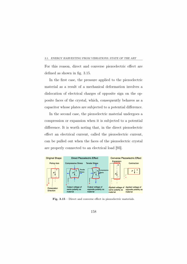
3.1. ENERGY HARVESTING FROM VIBRATIONS: STATE OF THE ART
For this reason, direct and converse piezoelectric effect are
defined as shown in fig. 3.15.
In the first case, the pressure applied to the piezoelectric
material as a result of a mechanical deformation involves a
dislocation of electrical charges of opposite sign on the op-
posite faces of the crystal, which, consequently behaves as a
capacitor whose plates are subjected to a potential difference.
In the second case, the piezoelectric material undergoes a
compression or expansion when it is subjected to a potential
difference. It is worth noting that, in the direct piezoelectric
effect an electrical current, called the piezoelectric current,
can be pulled out when the faces of the piezoelectric crystal
are properly connected to an electrical load [93].
Fig. 3.15 – Direct and converse effect in piezoelectric materials.
158
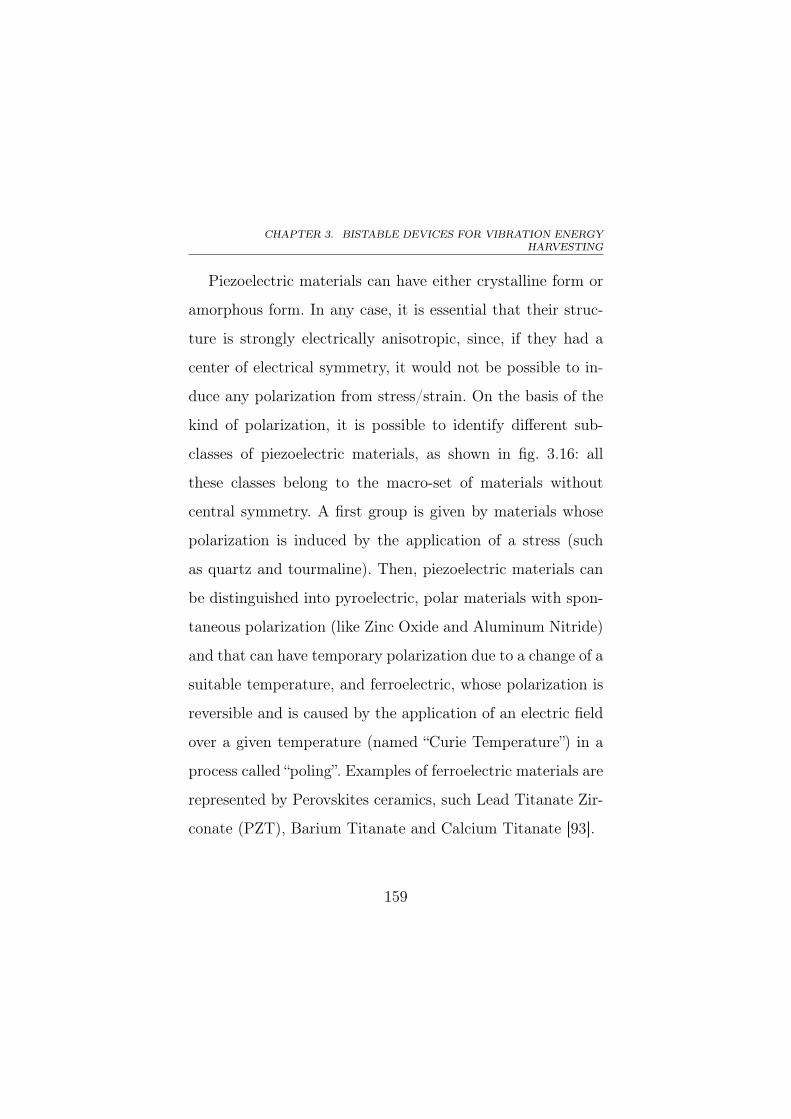
CHAPTER 3. BISTABLE DEVICES FOR VIBRATION ENERGYHARVESTING
Piezoelectric materials can have either crystalline form or
amorphous form. In any case, it is essential that their struc-
ture is strongly electrically anisotropic, since, if they had a
center of electrical symmetry, it would not be possible to in-
duce any polarization from stress/strain. On the basis of the
kind of polarization, it is possible to identify different sub-
classes of piezoelectric materials, as shown in fig. 3.16: all
these classes belong to the macro-set of materials without
central symmetry. A first group is given by materials whose
polarization is induced by the application of a stress (such
as quartz and tourmaline). Then, piezoelectric materials can
be distinguished into pyroelectric, polar materials with spon-
taneous polarization (like Zinc Oxide and Aluminum Nitride)
and that can have temporary polarization due to a change of a
suitable temperature, and ferroelectric, whose polarization is
reversible and is caused by the application of an electric field
over a given temperature (named “Curie Temperature”) in a
process called “poling”. Examples of ferroelectric materials are
represented by Perovskites ceramics, such Lead Titanate Zir-
conate (PZT), Barium Titanate and Calcium Titanate [93].
159
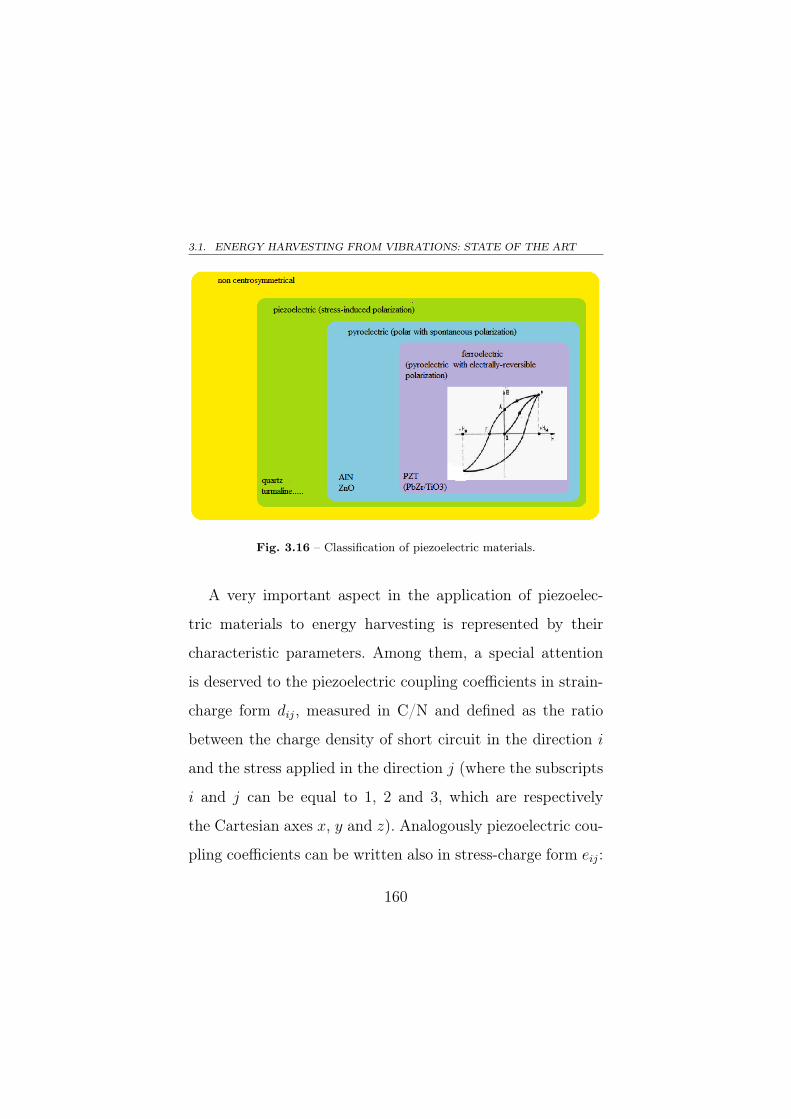
3.1. ENERGY HARVESTING FROM VIBRATIONS: STATE OF THE ART
Fig. 3.16 – Classification of piezoelectric materials.
A very important aspect in the application of piezoelec-
tric materials to energy harvesting is represented by their
characteristic parameters. Among them, a special attention
is deserved to the piezoelectric coupling coefficients in strain-
charge form dij, measured in C/N and defined as the ratio
between the charge density of short circuit in the direction i
and the stress applied in the direction j (where the subscripts
i and j can be equal to 1, 2 and 3, which are respectively
the Cartesian axes x, y and z). Analogously piezoelectric cou-
pling coefficients can be written also in stress-charge form eij:
160
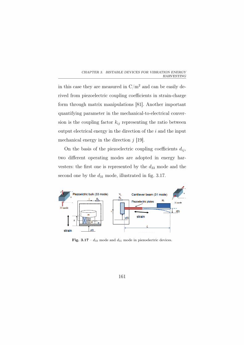
CHAPTER 3. BISTABLE DEVICES FOR VIBRATION ENERGYHARVESTING
in this case they are measured in C/m2 and can be easily de-
rived from piezoelectric coupling coefficients in strain-charge
form through matrix manipulations [81]. Another important
quantifying parameter in the mechanical-to-electrical conver-
sion is the coupling factor kij representing the ratio between
output electrical energy in the direction of the i and the input
mechanical energy in the direction j [19].
On the basis of the piezoelectric coupling coefficients dij,
two different operating modes are adopted in energy har-
vesters: the first one is represented by the d33 mode and the
second one by the d31 mode, illustrated in fig. 3.17.
Fig. 3.17 – d33 mode and d31 mode in piezoelectric devices.
161
3.1. ENERGY HARVESTING FROM VIBRATIONS: STATE OF THE ART
In d33 mode, a mechanical loading (e.g., a force or a stress)
is applied in the same direction as the poling direction and
a voltage/current is read in the same direction. An example
of piezoelectric structure operating in the d33 mode is repre-
sented by a membrane, whose piezoelectric layer is poled in
the direction orthogonal to the plane of the membrane; this
membrane is subjected to an orthogonal (with respect to the
plane of the membrane) mechanical loading and the electrical
output is “acquired” through two electrodes, one on the top
side of the piezoelectric layer and one on the bottom side.
In d31 mode, a mechanical loading (e.g., a force or a stress)
is applied in the direction perpendicular to the poling axis
and a voltage/current is read in the poling direction. An ex-
ample of piezoelectric structure operating in the d31 mode is
represented by a cantilever beam, whose piezoelectric layer is
poled in the direction orthogonal to the plane of the beam; in
this case, the beam is subjected to a loading on its free end
in the orthogonal direction and the consequently axial stress,
near the fixed end, generates an electrical output “acquired”
162
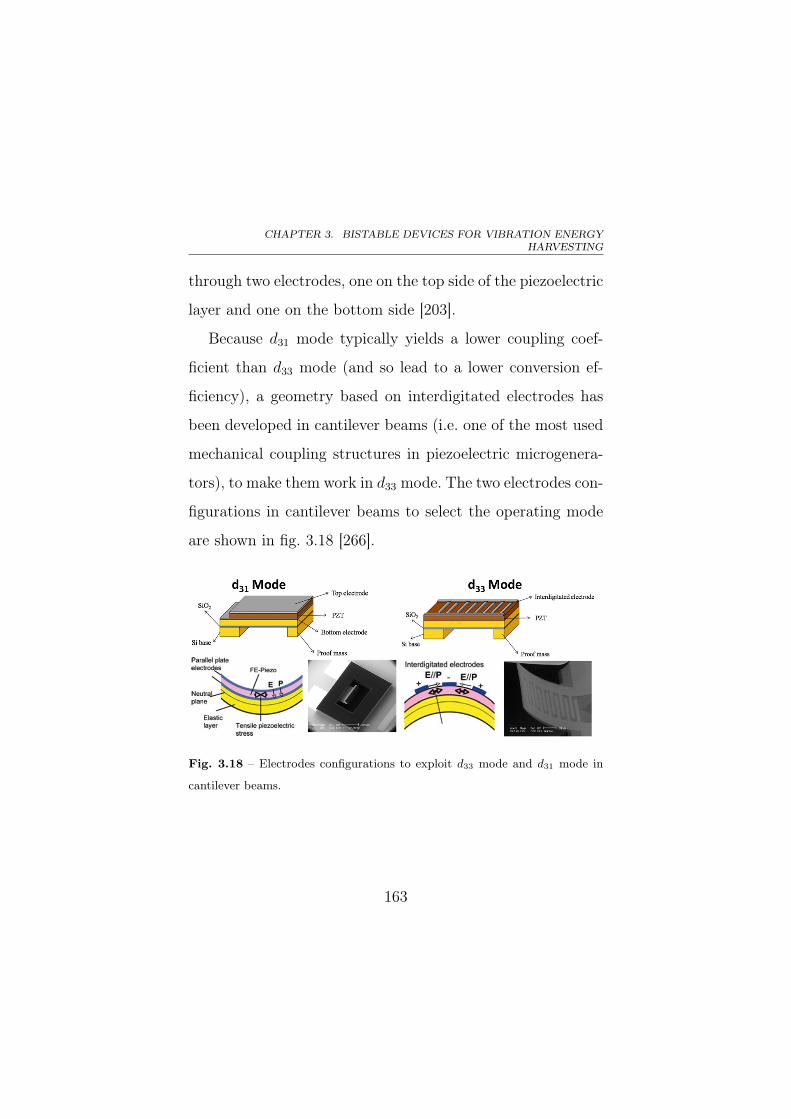
CHAPTER 3. BISTABLE DEVICES FOR VIBRATION ENERGYHARVESTING
through two electrodes, one on the top side of the piezoelectric
layer and one on the bottom side [203].
Because d31 mode typically yields a lower coupling coef-
ficient than d33 mode (and so lead to a lower conversion ef-
ficiency), a geometry based on interdigitated electrodes has
been developed in cantilever beams (i.e. one of the most used
mechanical coupling structures in piezoelectric microgenera-
tors), to make them work in d33 mode. The two electrodes con-
figurations in cantilever beams to select the operating mode
are shown in fig. 3.18 [266].
Fig. 3.18 – Electrodes configurations to exploit d33 mode and d31 mode in
cantilever beams.
163
3.1. ENERGY HARVESTING FROM VIBRATIONS: STATE OF THE ART
Many examples of piezoelectric energy harvesters based on
MEMS cantilever beams operating in d33 mode [120, 268] and
in d31 mode [54, 196] along some industrial microfabrication
process developments for piezoelectric devices [79, 174] can be
found in literature. Sometimes the sensitivity of the device to
mechanical vibrations is increased by adding a proof mass to
the free end of the beam [216]. Several attempts to improve
the power output of piezo-MEMS cantilever beams have been
studied, among them it has been proved that cantilever beams
with a trapezoidal (or triangular) shape exhibit a larger ax-
ial mechanical stress (and consequently the voltage output)
than beams having a rectangular shape [201]. Another im-
provement in the voltage output can be achieved from the
implementation of bimorph piezoelectric cantilever beam at
the cost of higher complexity [80].
An example of lumped parameter 1 DOF modeling of a
simple piezoelectric cantilever beam operating in d31 mode is
presented in (3.7) [81] and obtained by adding the mechanical-
to-electrical piezoelectric transduction to the (3.1).
164
CHAPTER 3. BISTABLE DEVICES FOR VIBRATION ENERGYHARVESTING
mz + cmz + kz − θV = −my
V = − θ
Cp˙z − 1
RLCpV
(3.7)
where θ is the piezoelectric coupling term for the beam and
it is defined as θ = −e31wp [81], in which wp is the width of the
piezoelectric layer in the cantilever beam. Other parameters
in (3.7) are V , state variable defining the output voltage of
the generator, ˙z, the first derivative of the axial strain (i.e.
the axial velocity of the strain) at the fixed end of the beam,
RL, the electrical load resistance attached to the generator
and Cp, the piezoelectric capacitance, defined in (3.8) [81].
Cp =ε33weletp
(3.8)
where ε33 is the electrical permittivity in the 33 direction
of the piezoelectric material, tp is the thickness of the piezo-
electric layer and we and le are respectively width and length
of the electrodes used in the piezo-stack to read the voltage
difference V generated by the piezoelectric layer.
An important result from (3.7) is the dependence of the
piezoelectric output voltage on the velocity in the axial strain
˙z. This means that the power output from piezoelectric scav-
165
3.1. ENERGY HARVESTING FROM VIBRATIONS: STATE OF THE ART
engers can be improved by both increasing strains in mechani-
cal coupling structures and augmenting velocity in their move-
ments. For this reason nonlinear coupling structures, espe-
cially bistable devices, leading to both larger strains and veloc-
ities than linear strictures, have been studied to be used in en-
ergy harvesters adopting piezoelectric mechanical-to-electrical
transduction [107].
Other examples of piezoelectric microgenerators make use
of other mechanical coupling structures such as clamped-
clamped beams [102], plates [57], “cymbals” [127], “wind-
mills” [188] and so on [205].
Piezoelectric transduction is also very promising for the im-
plementation of nanogenerators exploiting nanostructures like
arrays of nanowires and nanorods composed of piezoelectric
materials (zinc oxide and lead titanate zirconate) [190, 246].
Due to the large nonlinear strains, the high density of nanos-
tructures per volume unit and the exploitation of the benefits
of other effects at nanoscale, nanogenerators can provide bet-
ter performance than microgenerators in the future [260].
166

CHAPTER 3. BISTABLE DEVICES FOR VIBRATION ENERGYHARVESTING
Advantages of the piezoelectric mechanical-to-electrical trans-
duction in vibration energy harvesting are represented by [19]:
• high energy density;
• self-generating behaviour (i.e. they do no need an external
energy source to work);
• direct conversion from mechanical input;
• possibility of microfabricating thin films of piezoelectric
materials (e.g., Zinc Oxide, Lead Titanate Zirconate and
Aluminum Nitride).
However, some disadvantages descend from [19]:
• poor coupling coefficient of some thin piezoelectric films;
• depolarization and ageing problems (reduced performance
after long and heavy uses);
• charge leakage and high output impedance;
• operation in predefined single direction because of polar-
ization;
• complexity and sometimes incompatibility with standard
microfabrication process of piezoelectric thin film deposi-
tion techniques (requirement of high temperatures, high
film stress, etc.).
167
3.1. ENERGY HARVESTING FROM VIBRATIONS: STATE OF THE ART
Electrostatic transduction strategies
Electrostatic transducers use electrostatic forces Fel be-
tween charges stored on electrodes to couple energy from the
mechanical domain into the electric domain. The charge sep-
aration Q on the electrodes depends on the electric potential
difference V between them through the constitutive equation
of a capacitance Cv in (3.9) [212].
Q = CvV (3.9)
The capacitance Cv is a function of the geometry of the
electrodes and the characteristics of the materials surrounding
them. For this reason, capacitance represents the coupling be-
tween mechanical and electric fields in the electrostatic trans-
duction. As moving parts (e.g., the proof mass or shuttles)
of mechanical coupling structures displace due to external
vibrations, the capacitance Cv changes its value, sometimes
oscillating between a maximum value Cmax and a minimum
value Cmin. The electrical energy extracted from the mechan-
ical motion then depends strongly on the capacitance Cv vari-
168
CHAPTER 3. BISTABLE DEVICES FOR VIBRATION ENERGYHARVESTING
ation during time and on how the variable capacitance Cv is
connected to the electronic circuitry [157].
The microfabrication of integrated variable capacitances
has been standardized in the field of microsystems both
through surface micromachining techniques and bulk micro-
machining processes [3, 131]. These capacitors has been widely
used in the implementation of the capacitive readout in some
sensors like accelerometers and gyroscopes and in the realiza-
tion of comb drive electrostatic actuators (especially in gy-
roscopes) in MEMS industry [242]. Their development allows
for the operation in the three cartesian axes in a single mi-
crodevice [164].
Integrated variable capacitors can be exploited in imple-
menting energy harvesters based on electrostatic mechanical-
to-electrical transduction by adding them to the mechanical
oscillating structures. Depending on the direction of the mo-
tion and on the implementation of the capacitances, three
kinds of integrated capacitance configurations have been iden-
tified in literature [27] and illustrated in fig. 3.19: in-plane
169
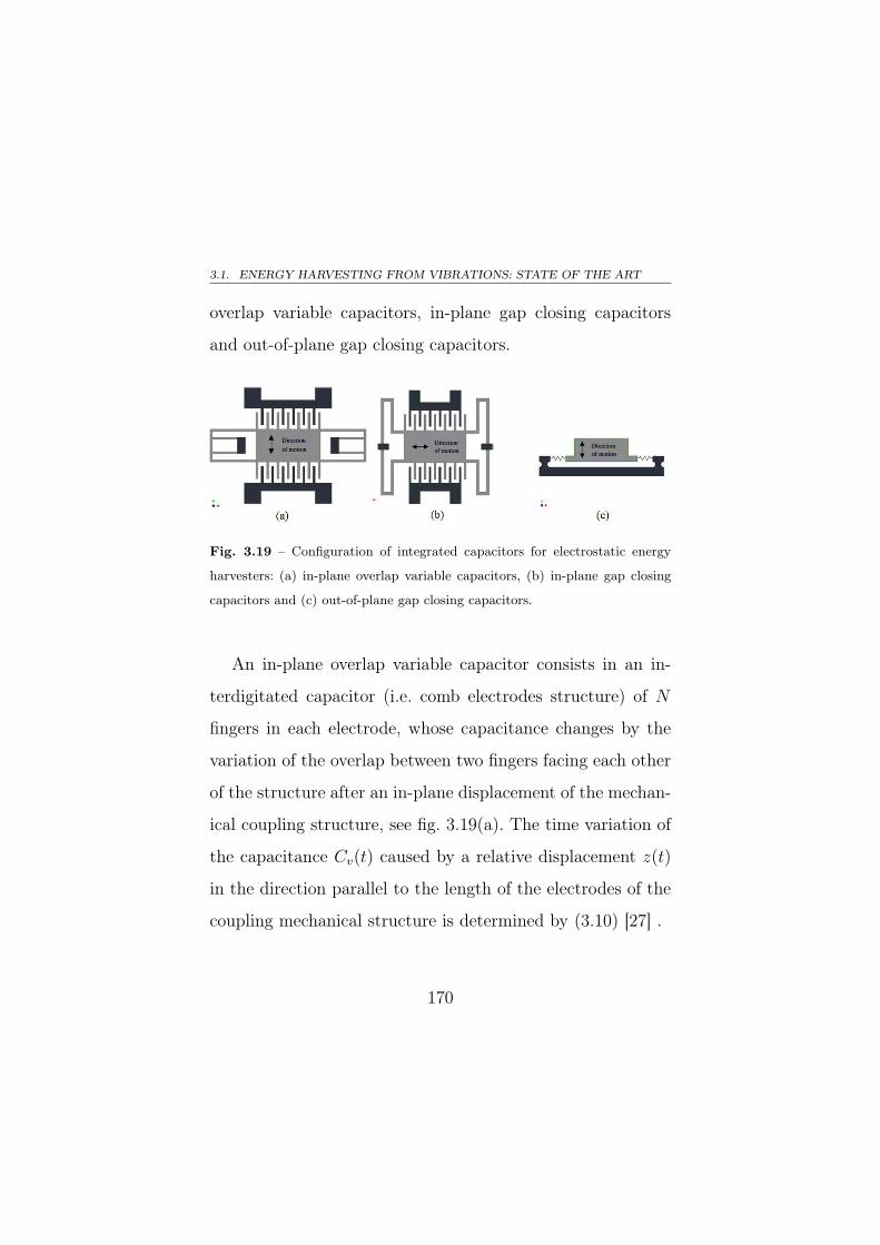
3.1. ENERGY HARVESTING FROM VIBRATIONS: STATE OF THE ART
overlap variable capacitors, in-plane gap closing capacitors
and out-of-plane gap closing capacitors.
Fig. 3.19 – Configuration of integrated capacitors for electrostatic energy
harvesters: (a) in-plane overlap variable capacitors, (b) in-plane gap closing
capacitors and (c) out-of-plane gap closing capacitors.
An in-plane overlap variable capacitor consists in an in-
terdigitated capacitor (i.e. comb electrodes structure) of N
fingers in each electrode, whose capacitance changes by the
variation of the overlap between two fingers facing each other
of the structure after an in-plane displacement of the mechan-
ical coupling structure, see fig. 3.19(a). The time variation of
the capacitance Cv(t) caused by a relative displacement z(t)
in the direction parallel to the length of the electrodes of the
coupling mechanical structure is determined by (3.10) [27] .
170
CHAPTER 3. BISTABLE DEVICES FOR VIBRATION ENERGYHARVESTING
Cv(t) = 2Nεt[l0 ± z(t)]
g(3.10)
where N is the number of fingers of each comb electrode, t
is the thickness of the capacitance fingers, l0 is the fabrication
overlap (i.e. when z(t) = 0) between two fingers facing each
other and g is the gap between the electrodes of the capaci-
tance.
An in-plane gap closing capacitor consists in an interdig-
itated capacitor (i.e. comb electrodes structure) of N fingers
in each electrode, whose capacitance changes by the varia-
tion of the gap of the electrodes of the capacitor after an
in-plane displacement of the mechanical coupling structure,
see fig. 3.19(b). The time variation of the capacitance Cv(t)
caused by a relative displacement z(t) in the direction orthog-
onal to the length of the electrodes of the coupling mechanical
structure is determined by (3.11) [27] .
Cv(t) = 2Nεtl
g0 ± z(t)(3.11)
Differently from (3.10), in (3.11) l is the length of the of
the electrodes of the capacitance and g0 is the fabrication gap
(i.e. when z(t) = 0) between the electrodes of the capacitance.
171
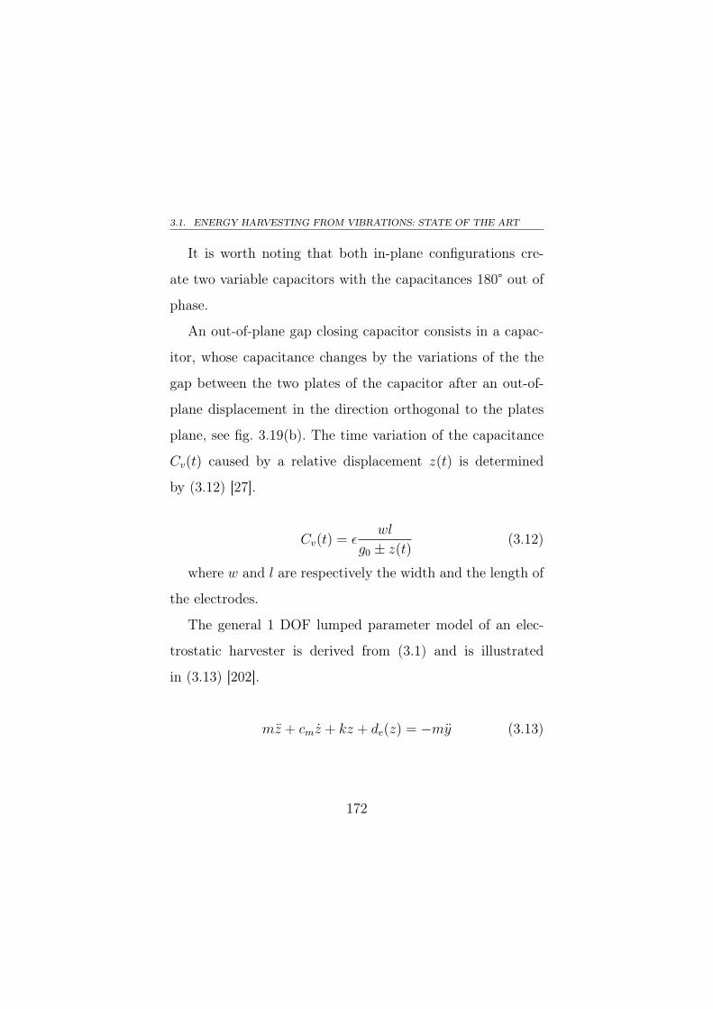
3.1. ENERGY HARVESTING FROM VIBRATIONS: STATE OF THE ART
It is worth noting that both in-plane configurations cre-
ate two variable capacitors with the capacitances 180° out of
phase.
An out-of-plane gap closing capacitor consists in a capac-
itor, whose capacitance changes by the variations of the the
gap between the two plates of the capacitor after an out-of-
plane displacement in the direction orthogonal to the plates
plane, see fig. 3.19(b). The time variation of the capacitance
Cv(t) caused by a relative displacement z(t) is determined
by (3.12) [27].
Cv(t) = εwl
g0 ± z(t)(3.12)
where w and l are respectively the width and the length of
the electrodes.
The general 1 DOF lumped parameter model of an elec-
trostatic harvester is derived from (3.1) and is illustrated
in (3.13) [202].
mz + cmz + kz + de(z) = −my (3.13)
172
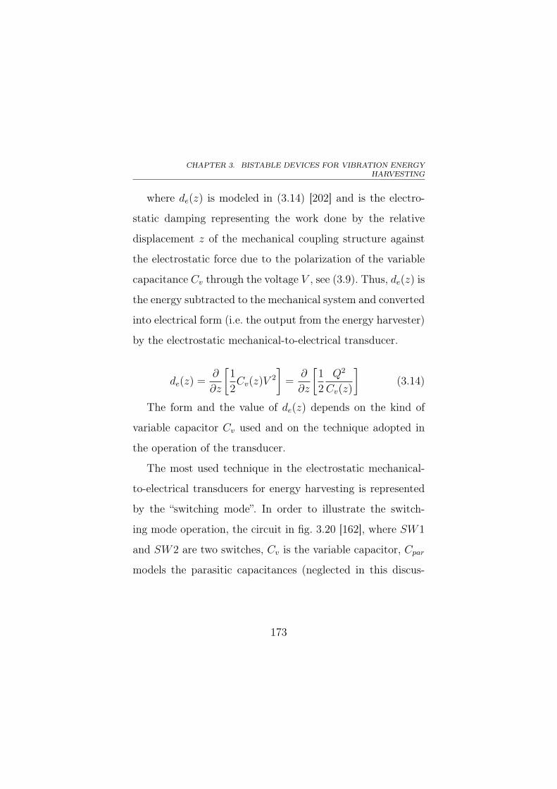
CHAPTER 3. BISTABLE DEVICES FOR VIBRATION ENERGYHARVESTING
where de(z) is modeled in (3.14) [202] and is the electro-
static damping representing the work done by the relative
displacement z of the mechanical coupling structure against
the electrostatic force due to the polarization of the variable
capacitance Cv through the voltage V , see (3.9). Thus, de(z) is
the energy subtracted to the mechanical system and converted
into electrical form (i.e. the output from the energy harvester)
by the electrostatic mechanical-to-electrical transducer.
de(z) =∂
∂z
[1
2Cv(z)V 2
]=
∂
∂z
[1
2
Q2
Cv(z)
](3.14)
The form and the value of de(z) depends on the kind of
variable capacitor Cv used and on the technique adopted in
the operation of the transducer.
The most used technique in the electrostatic mechanical-
to-electrical transducers for energy harvesting is represented
by the “switching mode”. In order to illustrate the switch-
ing mode operation, the circuit in fig. 3.20 [162], where SW1
and SW2 are two switches, Cv is the variable capacitor, Cpar
models the parasitic capacitances (neglected in this discus-
173
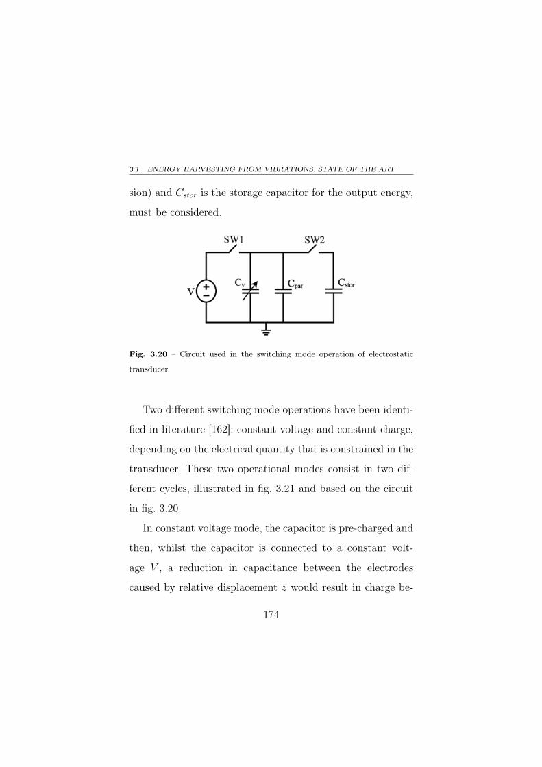
3.1. ENERGY HARVESTING FROM VIBRATIONS: STATE OF THE ART
sion) and Cstor is the storage capacitor for the output energy,
must be considered.
Fig. 3.20 – Circuit used in the switching mode operation of electrostatic
transducer
Two different switching mode operations have been identi-
fied in literature [162]: constant voltage and constant charge,
depending on the electrical quantity that is constrained in the
transducer. These two operational modes consist in two dif-
ferent cycles, illustrated in fig. 3.21 and based on the circuit
in fig. 3.20.
In constant voltage mode, the capacitor is pre-charged and
then, whilst the capacitor is connected to a constant volt-
age V , a reduction in capacitance between the electrodes
caused by relative displacement z would result in charge be-
174
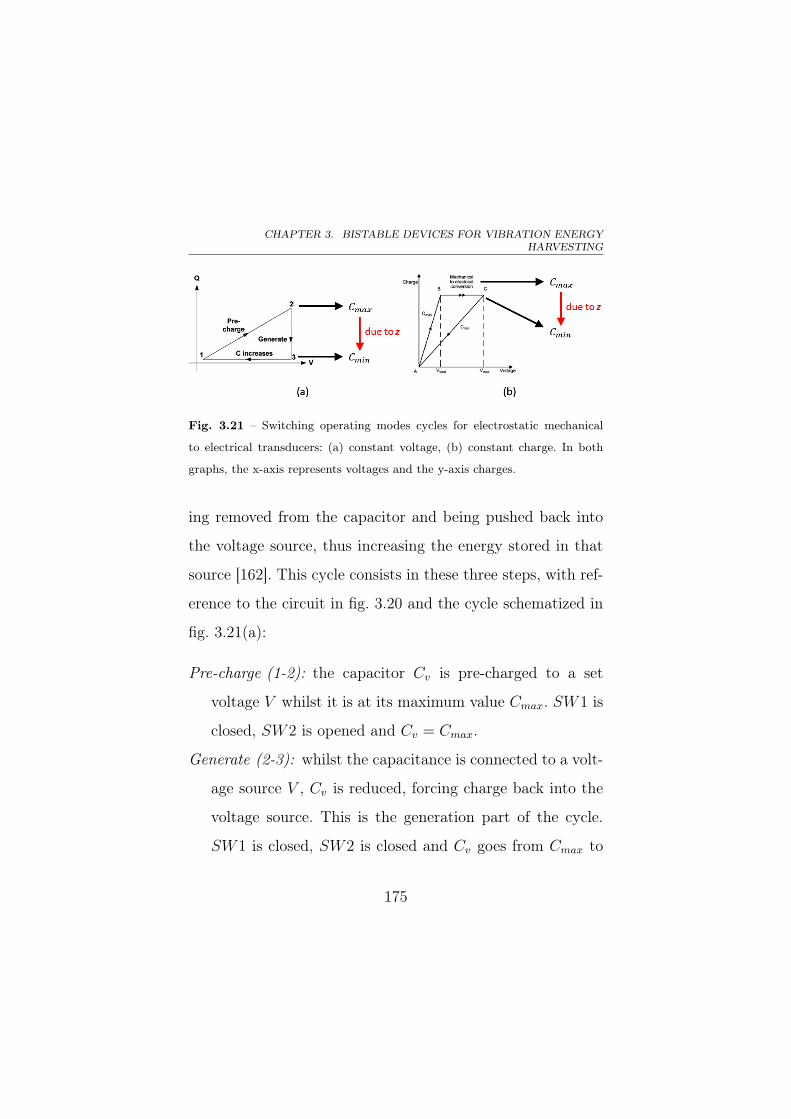
CHAPTER 3. BISTABLE DEVICES FOR VIBRATION ENERGYHARVESTING
Fig. 3.21 – Switching operating modes cycles for electrostatic mechanical
to electrical transducers: (a) constant voltage, (b) constant charge. In both
graphs, the x-axis represents voltages and the y-axis charges.
ing removed from the capacitor and being pushed back into
the voltage source, thus increasing the energy stored in that
source [162]. This cycle consists in these three steps, with ref-
erence to the circuit in fig. 3.20 and the cycle schematized in
fig. 3.21(a):
Pre-charge (1-2): the capacitor Cv is pre-charged to a set
voltage V whilst it is at its maximum value Cmax. SW1 is
closed, SW2 is opened and Cv = Cmax.
Generate (2-3): whilst the capacitance is connected to a volt-
age source V , Cv is reduced, forcing charge back into the
voltage source. This is the generation part of the cycle.
SW1 is closed, SW2 is closed and Cv goes from Cmax to
175
3.1. ENERGY HARVESTING FROM VIBRATIONS: STATE OF THE ART
Cmin because of the relative displacement z of the mechan-
ical coupling structure.
C increases (3-1): switches then disconnect Cv from the volt-
age source V before it is increased at constant charge (3-1)
ready for the cycle to start again. SW1 is opened, SW2 is
opened and Cv goes from Cmin to Cmax.
The area enclosed by the vertex 1, 2 and 3 in the Charge-
Voltage diagram in fig. 3.21(a) represents the electrical energy
E harvested in a cycle and is modeled in (3.15), where para-
sitic effects have been neglected.
E =1
2(Cmax − Cmin)V 2 (3.15)
In the constant charge mode, the variable capacitor Cv is
pre-charged at maximum capacitance Cmax and then discon-
nected from any external circuitry before the geometry of the
capacitor is changed by the relative displacement z of the me-
chanical coupling structure, additional energy will be stored
in the electric field between the electrodes as work has been
done against the electrostatic force [162]. This cycle consists
176
CHAPTER 3. BISTABLE DEVICES FOR VIBRATION ENERGYHARVESTING
in these three steps, with reference to the circuit in fig. 3.20
and the cycle schematized in fig. 3.21(b):
Pre-charge (A-B): the capacitor Cv is pre-charged to a low
voltage Vstart by making a connection to a voltage source.
SW1 is closed, SW2 is opened and Cv = Cmax.
Generate (B-C): the capacitor Cv is disconnected from the
source and the load in order to be separated under constant
charge during this part of the cycle. This is the generation
part of the cycle. SW1 is opened, SW2 is opened, Cv goes
from Cmax to Cmin because of the relative displacement z
of the mechanical coupling structure and the voltage goes
from Vstart to Vmax.
C discharge (C-A): The capacitor Cv is discharged to the load
Cstor in the third part of the cycle. The capacitance is then
increased ready for the cycle to restart. SW1 is opened,
SW2 is closed. When V = 0, Cv goes from Cmin to Cmax
due to the relative displacement z of the mechanical cou-
pling structure.
The area enclosed by the vertex A, B and C in the Charge-
Voltage diagram in fig. 3.21(b) represents the electrical energy
177
3.1. ENERGY HARVESTING FROM VIBRATIONS: STATE OF THE ART
E harvested in a cycle and is modeled in (3.16), where para-
sitic effects have been neglected.
E =1
2(CminVmax
2 − CmaxVstart2) (3.16)
By considering (3.15) and (3.16), larger applied voltages
V lead to larger energy extracted in a cycle, even if more
energy must be initially supplied to polarize the capacitance
Cv. Besides, larger displacements of the mechanical coupling
structure result in a larger energy output.
Several devices adopting switching operating modes have
been proposed in literature [112, 136], even if they exhibit
many limits.
First of all, electrostatic switching transducers require the
application of an external voltage to polarize the variable ca-
pacitances. Furthermore, there is the necessity of a control
logic to handle the polarization and the depolarization of the
capacitance Cv (i.e. the opening and the closing of the switches
SW1 and SW2 in the circuit in fig. 3.20); this requires the use
of electronics circuits, increasing design complexity and power
requirement of electrostatic harvesters. Mechanical switches
178
CHAPTER 3. BISTABLE DEVICES FOR VIBRATION ENERGYHARVESTING
are one of the solutions proposed in literature to help in solv-
ing the issue of the polarization and depolarization control
of the capacitance Cv [52]. Another issue is given by the ne-
cessity of knowing (or sensing) the values of Cmin and Cmax
in order to effectively control the polarization and the depo-
larization during the cycles. This limits, first of all, the de-
sign of the structures because mechanical stoppers must be
designed in order to limits the relative displacement z(t) of
the mechanical coupling structure. Secondly, this restricts the
range of application of these transducers because the han-
dling of sources of mechanical vibrations having a random
dynamics could be problematic for the effective control of po-
larization/depolarization of the capacitances; in fact, quite all
the examples in literature adopt deterministic inputs in labo-
ratory characterization, such as sinusoids [160], to model the
vibrational sources.
The aforesaid limitations have been overcome by the use
of variable capacitances having a fixed internal charge given
by electrets [32].
179
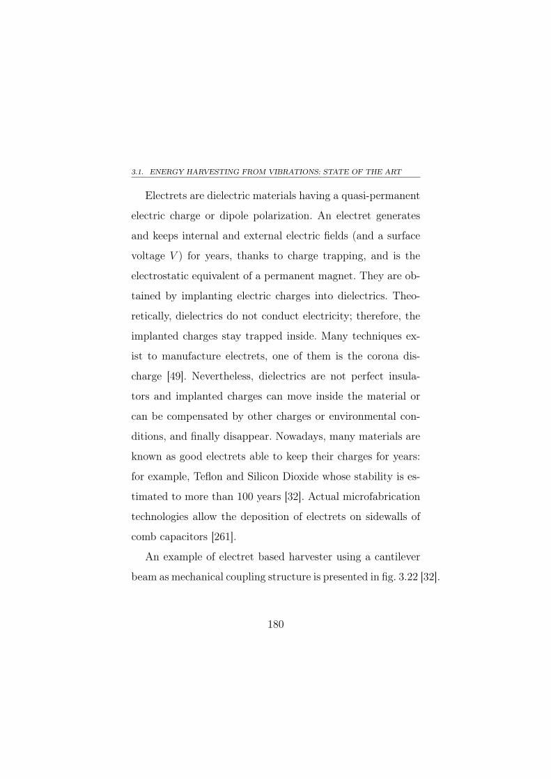
3.1. ENERGY HARVESTING FROM VIBRATIONS: STATE OF THE ART
Electrets are dielectric materials having a quasi-permanent
electric charge or dipole polarization. An electret generates
and keeps internal and external electric fields (and a surface
voltage V ) for years, thanks to charge trapping, and is the
electrostatic equivalent of a permanent magnet. They are ob-
tained by implanting electric charges into dielectrics. Theo-
retically, dielectrics do not conduct electricity; therefore, the
implanted charges stay trapped inside. Many techniques ex-
ist to manufacture electrets, one of them is the corona dis-
charge [49]. Nevertheless, dielectrics are not perfect insula-
tors and implanted charges can move inside the material or
can be compensated by other charges or environmental con-
ditions, and finally disappear. Nowadays, many materials are
known as good electrets able to keep their charges for years:
for example, Teflon and Silicon Dioxide whose stability is es-
timated to more than 100 years [32]. Actual microfabrication
technologies allow the deposition of electrets on sidewalls of
comb capacitors [261].
An example of electret based harvester using a cantilever
beam as mechanical coupling structure is presented in fig. 3.22 [32].
180
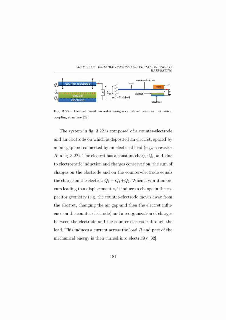
CHAPTER 3. BISTABLE DEVICES FOR VIBRATION ENERGYHARVESTING
Fig. 3.22 – Electret based harvester using a cantilever beam as mechanical
coupling structure [32].
The system in fig. 3.22 is composed of a counter-electrode
and an electrode on which is deposited an electret, spaced by
an air gap and connected by an electrical load (e.g., a resistor
R in fig. 3.22). The electret has a constant charge Qi, and, due
to electrostatic induction and charges conservation, the sum of
charges on the electrode and on the counter-electrode equals
the charge on the electret: Qi = Q1+Q2. When a vibration oc-
curs leading to a displacement z, it induces a change in the ca-
pacitor geometry (e.g. the counter-electrode moves away from
the electret, changing the air gap and then the electret influ-
ence on the counter electrode) and a reorganization of charges
between the electrode and the counter-electrode through the
load. This induces a current across the load R and part of the
mechanical energy is then turned into electricity [32].
181
3.1. ENERGY HARVESTING FROM VIBRATIONS: STATE OF THE ART
This system can be modeled through the 1 DOF lumped
parameter model, derived from (3.1) and exposed in (3.17) [32].
mz + cmz + kz − ∂
∂z
(Q2
2Cv
)= −my
∂Q
∂t=V
R− Q
RCv
Cv = εlEwE
[g0 ± z]
(3.17)
where Q is the charge on the electret, V surface voltage on
the electret, R the resistive load, lE the length of the capac-
itance plates, wE the length of the capacitance plates and g0
the initial gap between the capacitance plates. The electrical
output is given by the current ∂Q∂t.
Several examples of electret based devices can be found
in literature [33, 230] and a special attention is deserved to
harvesters having three axes scavenging capability [158].
Electromagnetic transduction strategies
Electromagnetic mechanical-to-electrical transducers ex-
ploit the electromagnetic induction phenomenon [212]. In this
case, an electro-motive force is induced across a coil if the mag-
netic flux coupled to the inductor changes as a function of time
182
CHAPTER 3. BISTABLE DEVICES FOR VIBRATION ENERGYHARVESTING
and space. Typically, a magnetic field source (e.g., permanent
magnet) is attached to the mechanical coupling structure and
oscillates because of mechanical vibrations. If the resultant
time-varying magnetic flux couples a fixed solenoid/inductor
(and/or vice versa), a voltage difference is generated as out-
put [47].
Considering the model (3.1), a general model for a har-
vester adopting electromagnetic mechanical-to-electrical trans-
duction can be derived in (3.18) [189].
mz + cmz + kz +Demz = −my
−dΦdzz − (Rc +RL)i− Ldi
dt= 0
Dem =1
(Rc +RL)i+ Ldidt
(dΦ
dz
)2(3.18)
where Dem is the electromagnetic damping (i.e. the en-
ergy subtracted from the mechanical system), Rc the electric
resistance of the coils/solenoid, RL the resistive load, L the
inductance of the coils/solenoid, Φ the total magnetic flux
linkage and i the electrical output current induced in the
solenoid/coil. The output voltage is given by the product be-
tween the output current i and the load resistance RL.
183
3.1. ENERGY HARVESTING FROM VIBRATIONS: STATE OF THE ART
Several examples of electromagnetic MEMS generators can
be found in literature [28, 75, 208].
Advantages of electromagnetic transducers are represented
by [189]:
• no separate external voltage source is needed;
• no mechanical stops are requested;
• no smart materials are needed (with the exception of per-
manent magnets).
However disadvantages are given by [189]:
• bulky size;
• difficult to integrate with microsystems;
• difficulty in fabricating integrated coils.
A special case of electromagnetic transducers is represented
by the devices exploiting magnetostrictive materials.
Magnetostriction is a property of ferromagnetic materials
that causes them to change their physical shape under the in-
fluence of external magnetic fields. The inverse magnetostric-
tive effect (also known as Villari effect) is the name given to
the change of the magnetic susceptibility of a material when
184
CHAPTER 3. BISTABLE DEVICES FOR VIBRATION ENERGYHARVESTING
subjected to a mechanical stress. Magnetostrictive materials
can convert magnetic energy into kinetic energy, or the re-
verse. Examples of magnetostrictive materials are: Cobalt,
Terfenol-D, Galfenol and Metglas 2605SC®.
According to Villari effect, the application of a time vari-
able stress (in this case coming from a mechanical coupling
structure) to a magnetostrictive material causes a changing
magnetic field that induces an electro-motive force across
a coil/solenoid through magnetic induction, thus generating
electrical energy [245].
3.2 Bistable MEMS devices for vibration
energy harvesting in the CNM BESOI
process
The development of bistable strategies for energy har-
vesting from mechanical vibrations represents one of the
key research fields to improve the efficiency of MEMS scav-
engers [107].
185
3.2. BISTABLE MEMS DEVICES FOR VIBRATION ENERGY HARVESTINGIN THE CNM BESOI PROCESS
In this section, a novel approach involving purely mechan-
ical, fully-compliant, bistable MEMS devices in the BESOI
process (see subsection 2.1.1) from the CNM of Barcelona
(Spain) is proposed to improve the efficiency of vibration en-
ergy harvesters when wideband vibrations at low frequencies
(e.g., the frequency spectrum below 500 Hz, where vibrations
contain more energy [202]) have to be addressed.
MEMS devices resembling those considered in this section
have been proposed [179] as bistable switches [35, 236]: all
these mechanisms have been actuated by thermal, electro-
static forces or mechanical probes.
Differently from what has been previously proposed in lit-
erature, the bistable microstructures proposed in this section
are actuated by external random mechanical vibrations, which
result in forces acting on an inertial mass placed at the center
of the bistable micromechanism in order to make it “snap-
ping” from one stable equilibrium state to the other one when
target vibrations are taken as input. Both the MEMS inertial
mass displacements and velocities will be taken into account.
In fact these quantities are both crucial in the mechanical-
186
CHAPTER 3. BISTABLE DEVICES FOR VIBRATION ENERGYHARVESTING
to-electrical conversion step: whichever mechanism is used to
produce electrical energy, a higher response in terms of dis-
placement and velocity will result in a higher power harvested
from random vibrations.
The analytical model of the microsystem will be discussed
in the subsection 3.2.1. Numerical analyses and their results
will be presented in the subsection 3.2.2 about the behaviour
of the MEMS device. Afterwards, a realistic case study has
been considered taking into account the range of accelera-
tions that can be experienced in automotive applications and
a geometrically optimized structure for these applications is
proposed and compared with an “equivalent” monostable de-
vice in subsection 3.2.3. Finally, the mechanical-to-electrical
transduction will be discussed in subsection 3.2.4 taking into
account the electrostatic transduction principle.
3.2.1 Device modeling
The mechanical structure investigated here is composed of
a central mass (CM) connected, via two short flexural piv-
ots (LCFP and RCFP), to two slanted rigid links (LRL and
RRL). These links are joined, via two short flexural pivots
187
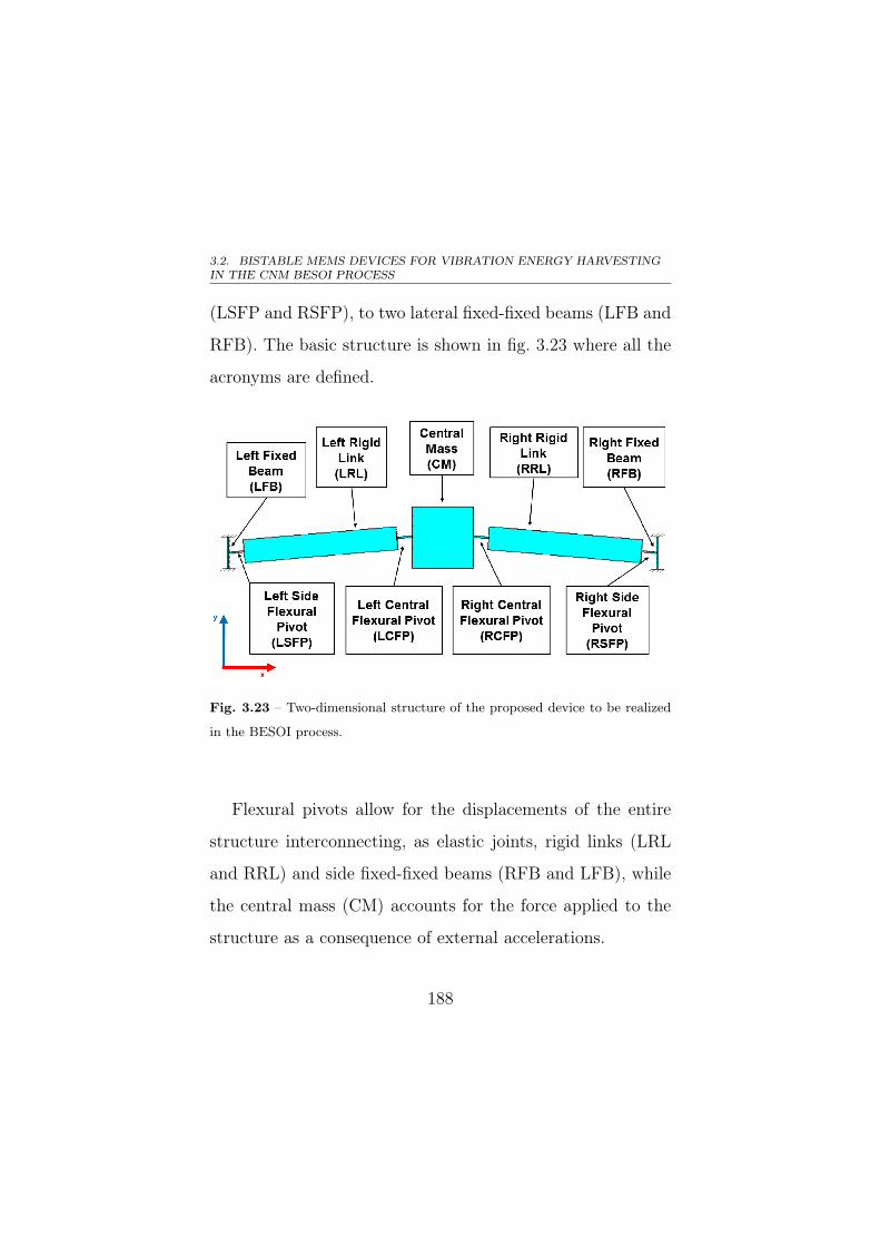
3.2. BISTABLE MEMS DEVICES FOR VIBRATION ENERGY HARVESTINGIN THE CNM BESOI PROCESS
(LSFP and RSFP), to two lateral fixed-fixed beams (LFB and
RFB). The basic structure is shown in fig. 3.23 where all the
acronyms are defined.
Fig. 3.23 – Two-dimensional structure of the proposed device to be realized
in the BESOI process.
Flexural pivots allow for the displacements of the entire
structure interconnecting, as elastic joints, rigid links (LRL
and RRL) and side fixed-fixed beams (RFB and LFB), while
the central mass (CM) accounts for the force applied to the
structure as a consequence of external accelerations.
188
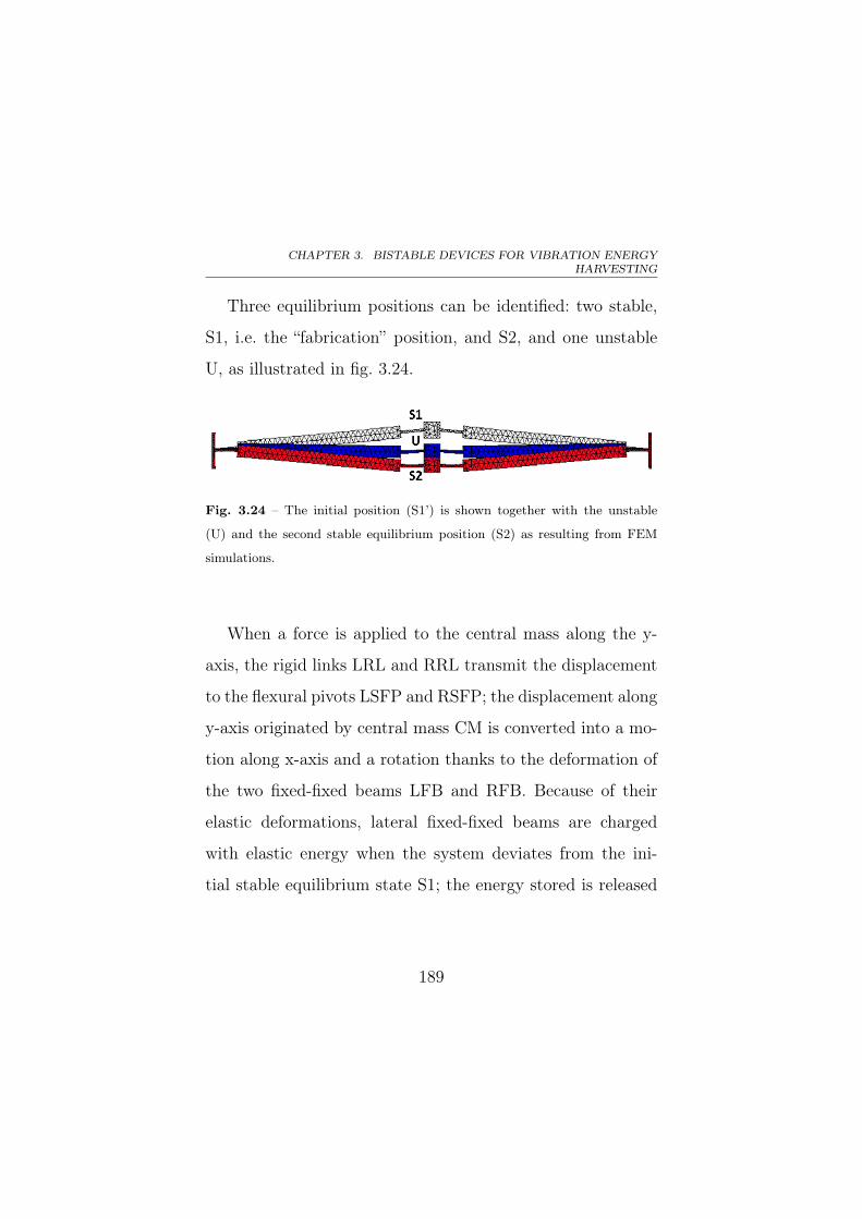
CHAPTER 3. BISTABLE DEVICES FOR VIBRATION ENERGYHARVESTING
Three equilibrium positions can be identified: two stable,
S1, i.e. the “fabrication” position, and S2, and one unstable
U, as illustrated in fig. 3.24.
Fig. 3.24 – The initial position (S1’) is shown together with the unstable
(U) and the second stable equilibrium position (S2) as resulting from FEM
simulations.
When a force is applied to the central mass along the y-
axis, the rigid links LRL and RRL transmit the displacement
to the flexural pivots LSFP and RSFP; the displacement along
y-axis originated by central mass CM is converted into a mo-
tion along x-axis and a rotation thanks to the deformation of
the two fixed-fixed beams LFB and RFB. Because of their
elastic deformations, lateral fixed-fixed beams are charged
with elastic energy when the system deviates from the ini-
tial stable equilibrium state S1; the energy stored is released
189
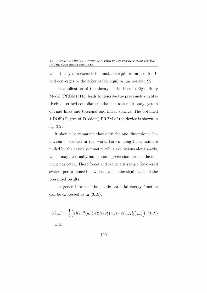
3.2. BISTABLE MEMS DEVICES FOR VIBRATION ENERGY HARVESTINGIN THE CNM BESOI PROCESS
when the system exceeds the unstable equilibrium position U
and converges to the other stable equilibrium position S2.
The application of the theory of the Pseudo-Rigid Body
Model (PRBM) [116] leads to describe the previously qualita-
tively described compliant mechanism as a multibody system
of rigid links and torsional and linear springs. The obtained
1 DOF (Degree of Freedom) PRBM of the device is shown in
fig. 3.25.
It should be remarked that only the one dimensional be-
haviour is studied in this work. Forces along the x-axis are
nulled by the device symmetry, while excitations along z-axis,
which may eventually induce some precession, are for the mo-
ment neglected. These forces will eventually reduce the overall
system performance but will not affect the significance of the
presented results.
The general form of the elastic potential energy function
can be expressed as in (3.19).
U(ym) =1
2
(2K1ψ
21
(ym)+2K2ψ
22
(ym)+2Ksbχ
2sb
(ym))
(3.19)
with:
190
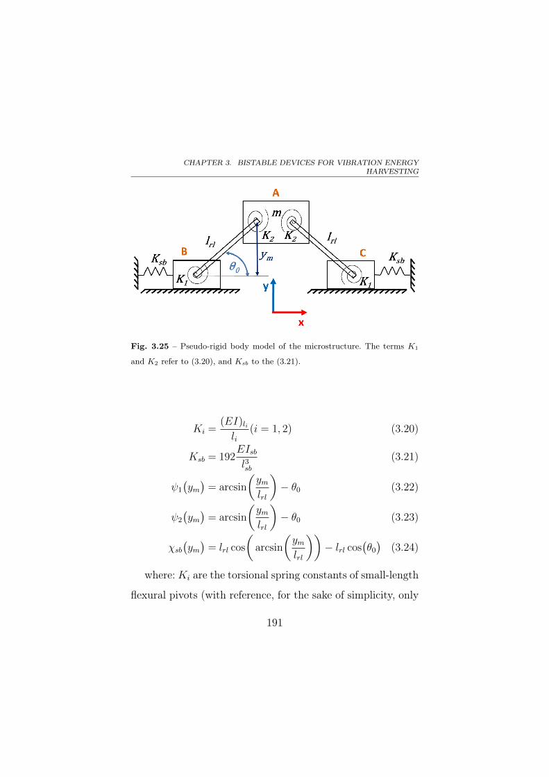
CHAPTER 3. BISTABLE DEVICES FOR VIBRATION ENERGYHARVESTING
Fig. 3.25 – Pseudo-rigid body model of the microstructure. The terms K1
and K2 refer to (3.20), and Ksb to the (3.21).
Ki =(EI)lili
(i = 1, 2) (3.20)
Ksb = 192EIsbl3sb
(3.21)
ψ1
(ym)
= arcsin
(ymlrl
)− θ0 (3.22)
ψ2
(ym)
= arcsin
(ymlrl
)− θ0 (3.23)
χsb(ym)
= lrl cos
(arcsin
(ymlrl
))− lrl cos
(θ0)
(3.24)
where:Ki are the torsional spring constants of small-length
flexural pivots (with reference, for the sake of simplicity, only
191
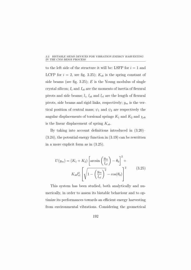
3.2. BISTABLE MEMS DEVICES FOR VIBRATION ENERGY HARVESTINGIN THE CNM BESOI PROCESS
to the left side of the structure it will be: LSFP for i = 1 and
LCFP for i = 2, see fig. 3.25); Ksb is the spring constant of
side beams (see fig. 3.25); E is the Young modulus of single
crystal silicon; Ii and Isb are the moments of inertia of flexural
pivots and side beams; li, lsb and lrl are the length of flexural
pivots, side beams and rigid links, respectively; ym is the ver-
tical position of central mass; ψ1 and ψ2 are respectively the
angular displacements of torsional springs K1 and K2 and χsb
is the linear displacement of spring Ksb.
By taking into account definitions introduced in (3.20)–
(3.24), the potential energy function in (3.19) can be rewritten
in a more explicit form as in (3.25).
U(ym) = (K1 +K2)
[arcsin
(ymlrl
)− θ0
]2+
Ksbl2rl
√1−(ymlrl
)2
− cos(θ0)
2 (3.25)
This system has been studied, both analytically and nu-
merically, in order to assess its bistable behaviour and to op-
timize its performances towards an efficient energy harvesting
from environmental vibrations. Considering the geometrical
192
CHAPTER 3. BISTABLE DEVICES FOR VIBRATION ENERGYHARVESTING
dimensions of the proposed microstructure as design parame-
ters (they are listed in table 3.4), an accurate parameter anal-
ysis has been performed in order to characterize the effects of
the bistable behaviour.
An optimization has been carried out over several parame-
ters in order to minimize the acceleration necessary to obtain
the switching behaviour between the two stable equilibrium
configurations and the resulting set of values is reported in ta-
ble 3.4. Design rules and the mechanical material properties
(see table 3.3) of the structural layer in the BESOI process
described in subsection 3.2.3 have been taken into account as
design constraints.
Table 3.3 – Mechanical material properties of single crystal silicon [213] in
BESOI technology.
Properties Value
Mass density 2330 kg/m3
Young modulus 169 GPa
Poisson’s ratio 0.3
193

3.2. BISTABLE MEMS DEVICES FOR VIBRATION ENERGY HARVESTINGIN THE CNM BESOI PROCESS
Results of the parameter analysis are reported in table 3.4
and a scheme of the variables listed in table 3.4 is shown in
fig. 3.26.
Table 3.4 – Geometric parameters of the microstructure in fig. 3.23. The
microstructure is symmetric along y-axis. A basic schematic of the variables
listed is shown in fig. 3.26.
Variable Value Description
θ0 5.5° Slope of rigid links and flexural pivots
lsfp 200 µm Length of side flexural pivots
lrl 1500 µm Length of rigid links
lcfp 200 µm Length of central flexural pivots
lsb 150 µm Length of side beams
wsfp 10 µm Width of side flexural pivots
wrl 70 µm Width of rigid links
wcfp 10 µm Width of central flexural pivots
wsb 10 µm Width of side beams
t 15 µm Thickness (except the central mass)
tcm 467 µm Thickness of the central mass
The parameters values in table 3.4 have been used to
evaluate the elastic potential energy function U(ym) through
194
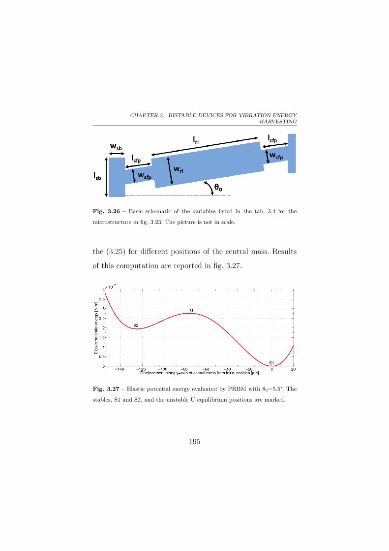
CHAPTER 3. BISTABLE DEVICES FOR VIBRATION ENERGYHARVESTING
Fig. 3.26 – Basic schematic of the variables listed in the tab. 3.4 for the
microstructure in fig. 3.23. The picture is not in scale.
the (3.25) for different positions of the central mass. Results
of this computation are reported in fig. 3.27.
Fig. 3.27 – Elastic potential energy evaluated by PRBM with θ0=5.5°. The
stables, S1 and S2, and the unstable U equilibrium positions are marked.
195

3.2. BISTABLE MEMS DEVICES FOR VIBRATION ENERGY HARVESTINGIN THE CNM BESOI PROCESS
The bistable potential is not symmetrical, this is due to the
slope θ0 assigned as a design parameter to the junction be-
tween the flexures and the rigid links. This means that flexural
pivots are deflected in the second stable equilibrium position
S2 and, consequently, the torsional springs K1 and K2 are not
at rest and give a nonzero contribution to the elastic potential
energy. As a consequence, a higher energy threshold must be
overcome to switch from S1 to S2 than from S2 to S1. The
asymmetrical trend in fig. 3.27 can be seen as the sum of two
contributions: one, symmetrical, due to the spring Ksb and
another, asymmetrical, generated by torsional springs K1 and
K2.
Among all parameters, a special attention has been paid
to the angle θ0, that is the slope (referenced to the horizon-
tal axis) of the rigid links at the intersection with the side
beams. In fact, this angle is one of the fabrication parameters
that strongly affects the bistable behaviour, as can be later
in fig. 3.28 where several elastic potential energy functions
U(ym) for different values of the angle θ0.
196
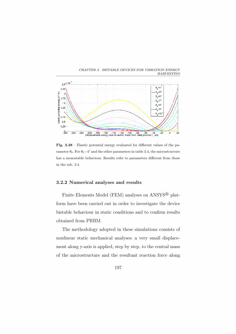
CHAPTER 3. BISTABLE DEVICES FOR VIBRATION ENERGYHARVESTING
Fig. 3.28 – Elastic potential energy evaluated for different values of the pa-
rameter θ0. For θ0=4° and the other parameters in table 3.4, the microstructure
has a monostable behaviour. Results refer to parameters different from those
in the tab. 3.4.
3.2.2 Numerical analyses and results
Finite Elements Model (FEM) analyses on ANSYS® plat-
form have been carried out in order to investigate the device
bistable behaviour in static conditions and to confirm results
obtained from PRBM.
The methodology adopted in these simulations consists of
nonlinear static mechanical analyses: a very small displace-
ment along y-axis is applied, step by step, to the central mass
of the microstructure and the resultant reaction force along
197
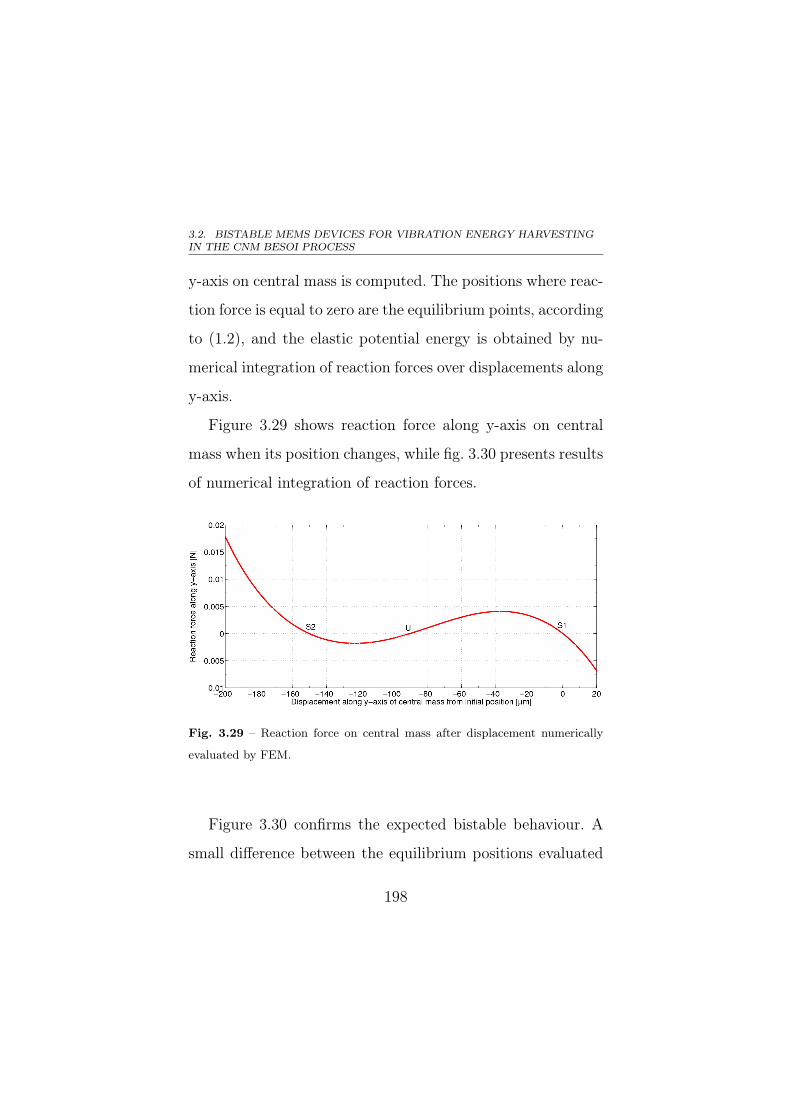
3.2. BISTABLE MEMS DEVICES FOR VIBRATION ENERGY HARVESTINGIN THE CNM BESOI PROCESS
y-axis on central mass is computed. The positions where reac-
tion force is equal to zero are the equilibrium points, according
to (1.2), and the elastic potential energy is obtained by nu-
merical integration of reaction forces over displacements along
y-axis.
Figure 3.29 shows reaction force along y-axis on central
mass when its position changes, while fig. 3.30 presents results
of numerical integration of reaction forces.
Fig. 3.29 – Reaction force on central mass after displacement numerically
evaluated by FEM.
Figure 3.30 confirms the expected bistable behaviour. A
small difference between the equilibrium positions evaluated
198
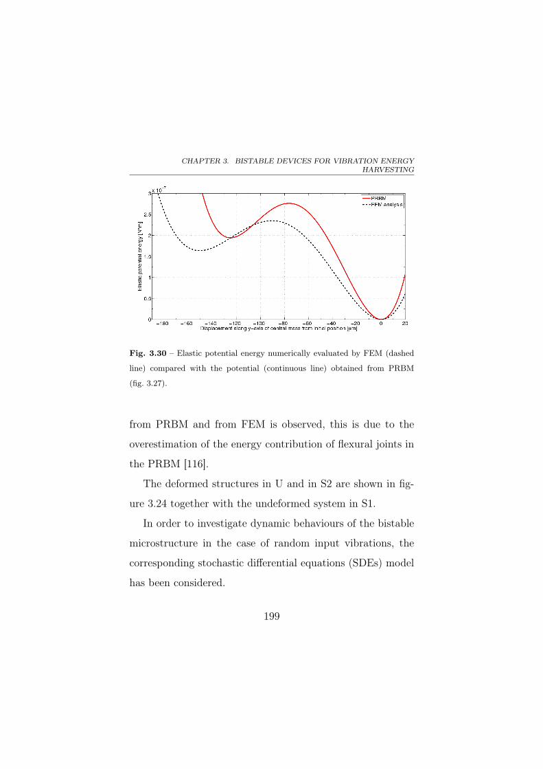
CHAPTER 3. BISTABLE DEVICES FOR VIBRATION ENERGYHARVESTING
Fig. 3.30 – Elastic potential energy numerically evaluated by FEM (dashed
line) compared with the potential (continuous line) obtained from PRBM
(fig. 3.27).
from PRBM and from FEM is observed, this is due to the
overestimation of the energy contribution of flexural joints in
the PRBM [116].
The deformed structures in U and in S2 are shown in fig-
ure 3.24 together with the undeformed system in S1.
In order to investigate dynamic behaviours of the bistable
microstructure in the case of random input vibrations, the
corresponding stochastic differential equations (SDEs) model
has been considered.
199
3.2. BISTABLE MEMS DEVICES FOR VIBRATION ENERGY HARVESTINGIN THE CNM BESOI PROCESS
The nonlinear dynamic model is indicated in (3.26) and
derived from (3.5).
my + cy + Ψ(y) = −maext (3.26)
where m is the central mass of the system, c is the me-
chanical damping coefficient, y is the displacement of central
mass along y-axis with respect to the external frame, aext is
the input acceleration applied to the external frame and Ψ(y)
is the nonlinear elastic term expressed by (3.27):
Ψ(y) =dU(y)
dy(3.27)
where U(y) is the elastic potential energy function, evalu-
ated via a fourth-order polynomial fitting of the FEM results
shown in fig. 3.30.
From (3.26), the two-dimensional stochastic differential
equations system in Ito form [129] can be derived in (3.28):
dy = yvdt
dyv = 1m
[− cyv − Ψ(y)
]dt+ σ
mdWt
(3.28)
200
CHAPTER 3. BISTABLE DEVICES FOR VIBRATION ENERGYHARVESTING
where yv represents the velocity of the central mass,Wt rep-
resents the Wiener process, which increments by dWt. Wiener
process models the stochastic input due to external mechan-
ical random vibrations. Finally σ represents the diffusion co-
efficient which set the magnitude of the stochastic input aext
by (3.29) [139]. The input signal is therefore modeled as:
aext =σ
m
dWt
dt=σ
mεt
1√dt
(3.29)
where εt is a dimensionless, random, serially uncorrelated,
normally distributed variable.
The Euler-Maruyama method has been used to solve nu-
merically the SDEs model in (3.28) by using Matlab and to
evaluate the dynamic behaviour of the system [129]. Setting
σ = 12 µNs1/2, the integration time step ts is equal to 1 µs
and taking into account BESOI technology parameters, re-
sults shown in figs. 3.31–3.32 have been obtained and bistable
behaviour is evident in the simulated dynamics.
In order to compare the behaviour of the device proposed
with an equivalent monostable system, simulations bench-
marks have been performed by considering the same struc-
201
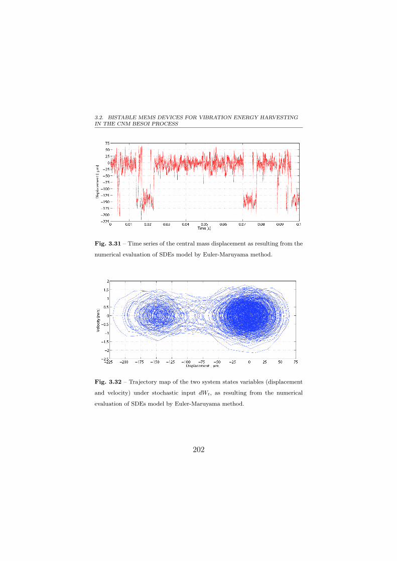
3.2. BISTABLE MEMS DEVICES FOR VIBRATION ENERGY HARVESTINGIN THE CNM BESOI PROCESS
Fig. 3.31 – Time series of the central mass displacement as resulting from the
numerical evaluation of SDEs model by Euler-Maruyama method.
Fig. 3.32 – Trajectory map of the two system states variables (displacement
and velocity) under stochastic input dWt, as resulting from the numerical
evaluation of SDEs model by Euler-Maruyama method.
202
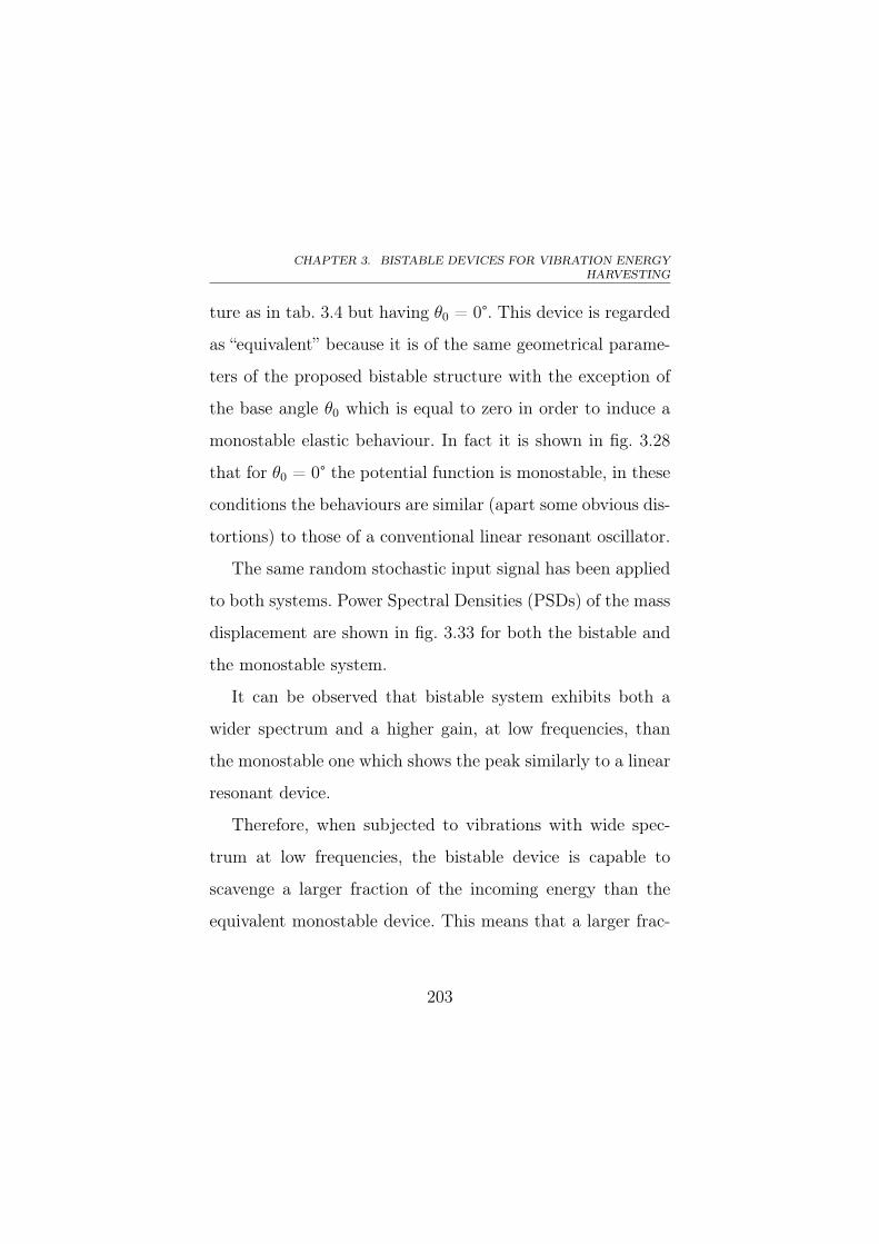
CHAPTER 3. BISTABLE DEVICES FOR VIBRATION ENERGYHARVESTING
ture as in tab. 3.4 but having θ0 = 0°. This device is regarded
as “equivalent” because it is of the same geometrical parame-
ters of the proposed bistable structure with the exception of
the base angle θ0 which is equal to zero in order to induce a
monostable elastic behaviour. In fact it is shown in fig. 3.28
that for θ0 = 0° the potential function is monostable, in these
conditions the behaviours are similar (apart some obvious dis-
tortions) to those of a conventional linear resonant oscillator.
The same random stochastic input signal has been applied
to both systems. Power Spectral Densities (PSDs) of the mass
displacement are shown in fig. 3.33 for both the bistable and
the monostable system.
It can be observed that bistable system exhibits both a
wider spectrum and a higher gain, at low frequencies, than
the monostable one which shows the peak similarly to a linear
resonant device.
Therefore, when subjected to vibrations with wide spec-
trum at low frequencies, the bistable device is capable to
scavenge a larger fraction of the incoming energy than the
equivalent monostable device. This means that a larger frac-
203
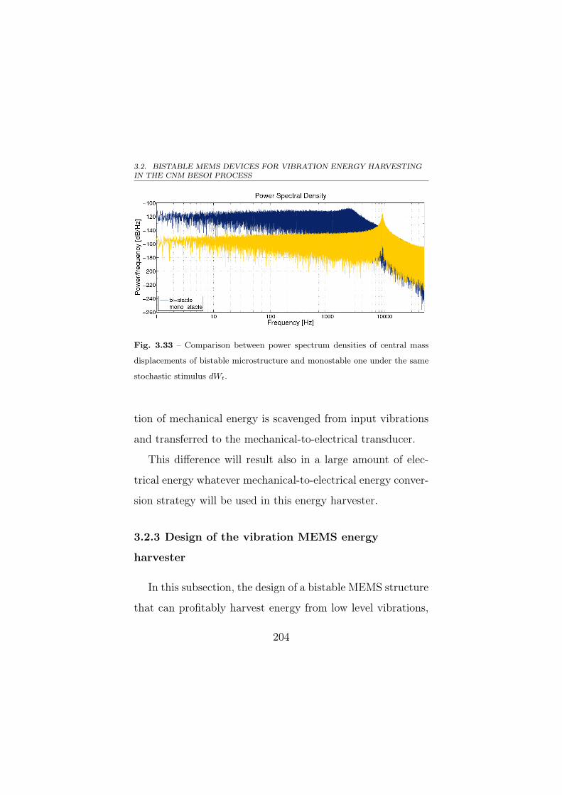
3.2. BISTABLE MEMS DEVICES FOR VIBRATION ENERGY HARVESTINGIN THE CNM BESOI PROCESS
Fig. 3.33 – Comparison between power spectrum densities of central mass
displacements of bistable microstructure and monostable one under the same
stochastic stimulus dWt.
tion of mechanical energy is scavenged from input vibrations
and transferred to the mechanical-to-electrical transducer.
This difference will result also in a large amount of elec-
trical energy whatever mechanical-to-electrical energy conver-
sion strategy will be used in this energy harvester.
3.2.3 Design of the vibration MEMS energy
harvester
In this subsection, the design of a bistable MEMS structure
that can profitably harvest energy from low level vibrations,
204
CHAPTER 3. BISTABLE DEVICES FOR VIBRATION ENERGYHARVESTING
whose energy is spread over a large bandwidth at low frequen-
cies, is proposed.
Several scenarios are considered, including automotive,
where vibrations appear as a noisy signal [202] with acceler-
ation peak of about 12 m/s2 and bandwidth of few hundreds
Hertz, eventually up to about 500 Hz.
The design goal is focused on a bistable MEMS device that
can show low critical forces, mechanical robustness, rejection
of unwanted vibrational modes and a limited occupation of
wafer area taking into account the BESOI technology param-
eters.
The worst case to allow switching between stable equilib-
rium states is represented by the critical force required to stat-
ically commutate from S1 to S2 and that can be evaluated by
FEM (see, for example, fig. 3.29 in the case of the previous
structure), while a more accurate estimation of the minimal
forces required to obtain switching must be performed by tak-
ing into account the dynamic behaviour. The design strategy
will be based on FEM simulations results to estimate the force
level to be applied to the inertial mass in order to induce
205
3.2. BISTABLE MEMS DEVICES FOR VIBRATION ENERGY HARVESTINGIN THE CNM BESOI PROCESS
switching between the two stable equilibrium states of the de-
vice; the worst case, represented by the commutation from
S1 to S2, will be obviously taken into account. The dynamic
behaviours will therefore be taken into account to refer these
results to the external acceleration aext.
The basic bistable structure studied in the previous section
has been considered as first device candidate. For this device
it has been not possible to satisfy all the design goals as the
minimum acceleration level required for inducing switchings
was larger than the considered design goal.
A modified structure has been therefore considered where
a different geometry for the flexural beam has been taken into
account in order to increase the device flexibility. The fixed-
fixed beams (LFB and RFB) have been replaced by a rigid
part (Left Rigid Part, LRP, and Right Rigid Part, RRP) in-
terconnecting respectively each of the original side flexural
pivots (LSFP and RSFP) to two flexural pivots (Left Side
Upper Flexural Pivot, LSUFP, and Left Side Lower Flexural
Pivot, LSLFP, Right Side Upper Flexural Pivot, RSUFP, and
Right Side Lower Flexural Pivot, RSLFP). These two addi-
206
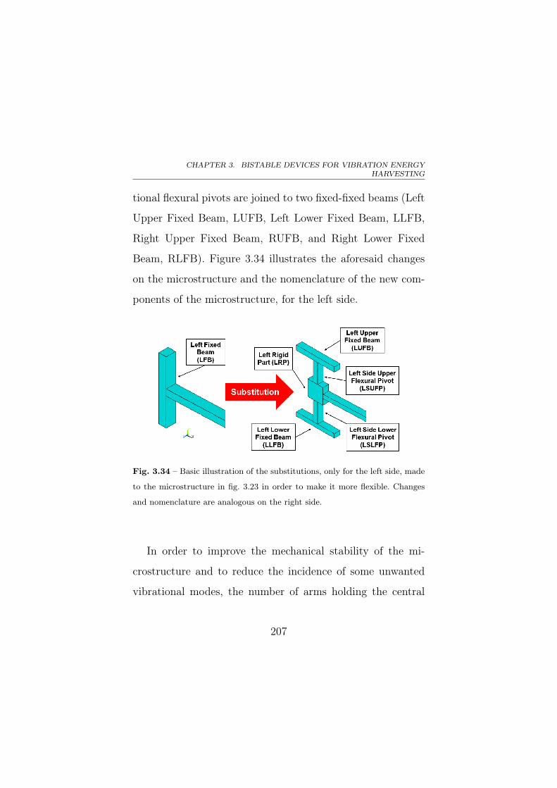
CHAPTER 3. BISTABLE DEVICES FOR VIBRATION ENERGYHARVESTING
tional flexural pivots are joined to two fixed-fixed beams (Left
Upper Fixed Beam, LUFB, Left Lower Fixed Beam, LLFB,
Right Upper Fixed Beam, RUFB, and Right Lower Fixed
Beam, RLFB). Figure 3.34 illustrates the aforesaid changes
on the microstructure and the nomenclature of the new com-
ponents of the microstructure, for the left side.
Fig. 3.34 – Basic illustration of the substitutions, only for the left side, made
to the microstructure in fig. 3.23 in order to make it more flexible. Changes
and nomenclature are analogous on the right side.
In order to improve the mechanical stability of the mi-
crostructure and to reduce the incidence of some unwanted
vibrational modes, the number of arms holding the central
207
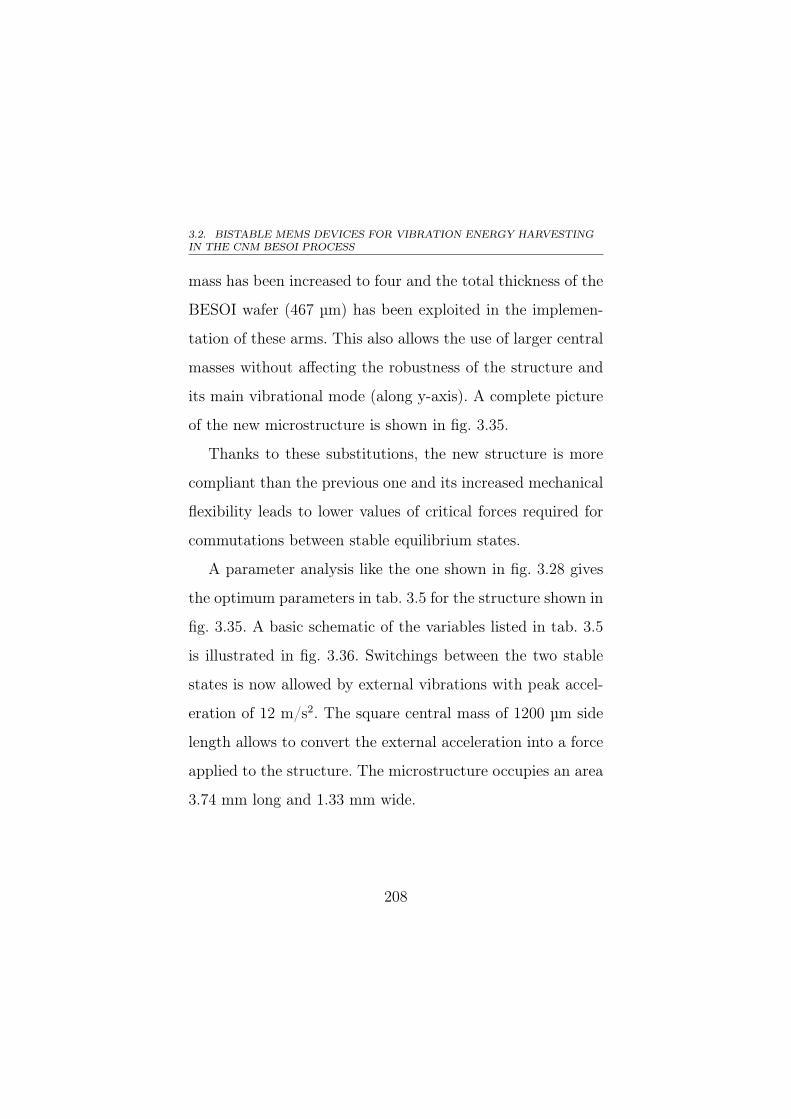
3.2. BISTABLE MEMS DEVICES FOR VIBRATION ENERGY HARVESTINGIN THE CNM BESOI PROCESS
mass has been increased to four and the total thickness of the
BESOI wafer (467 µm) has been exploited in the implemen-
tation of these arms. This also allows the use of larger central
masses without affecting the robustness of the structure and
its main vibrational mode (along y-axis). A complete picture
of the new microstructure is shown in fig. 3.35.
Thanks to these substitutions, the new structure is more
compliant than the previous one and its increased mechanical
flexibility leads to lower values of critical forces required for
commutations between stable equilibrium states.
A parameter analysis like the one shown in fig. 3.28 gives
the optimum parameters in tab. 3.5 for the structure shown in
fig. 3.35. A basic schematic of the variables listed in tab. 3.5
is illustrated in fig. 3.36. Switchings between the two stable
states is now allowed by external vibrations with peak accel-
eration of 12 m/s2. The square central mass of 1200 µm side
length allows to convert the external acceleration into a force
applied to the structure. The microstructure occupies an area
3.74 mm long and 1.33 mm wide.
208
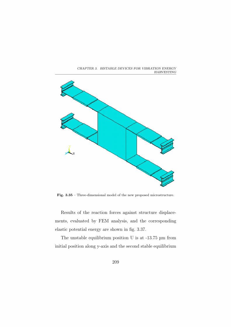
CHAPTER 3. BISTABLE DEVICES FOR VIBRATION ENERGYHARVESTING
Fig. 3.35 – Three-dimensional model of the new proposed microstructure.
Results of the reaction forces against structure displace-
ments, evaluated by FEM analysis, and the corresponding
elastic potential energy are shown in fig. 3.37.
The unstable equilibrium position U is at -13.75 µm from
initial position along y-axis and the second stable equilibrium
209
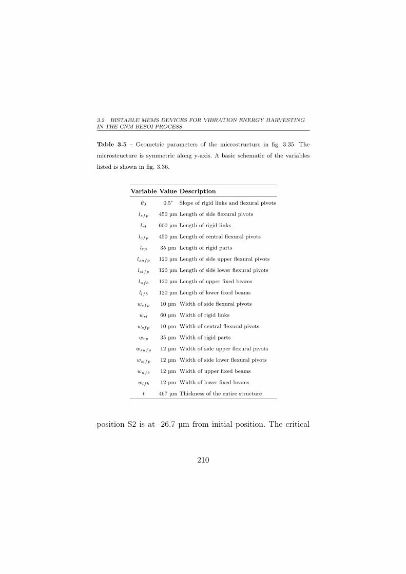
3.2. BISTABLE MEMS DEVICES FOR VIBRATION ENERGY HARVESTINGIN THE CNM BESOI PROCESS
Table 3.5 – Geometric parameters of the microstructure in fig. 3.35. The
microstructure is symmetric along y-axis. A basic schematic of the variables
listed is shown in fig. 3.36.
Variable Value Description
θ0 0.5° Slope of rigid links and flexural pivots
lsfp 450 µm Length of side flexural pivots
lrl 600 µm Length of rigid links
lcfp 450 µm Length of central flexural pivots
lrp 35 µm Length of rigid parts
lsufp 120 µm Length of side upper flexural pivots
lslfp 120 µm Length of side lower flexural pivots
lufb 120 µm Length of upper fixed beams
llfb 120 µm Length of lower fixed beams
wsfp 10 µm Width of side flexural pivots
wrl 60 µm Width of rigid links
wcfp 10 µm Width of central flexural pivots
wrp 35 µm Width of rigid parts
wsufp 12 µm Width of side upper flexural pivots
wslfp 12 µm Width of side lower flexural pivots
wufb 12 µm Width of upper fixed beams
wlfb 12 µm Width of lower fixed beams
t 467 µm Thickness of the entire structure
position S2 is at -26.7 µm from initial position. The critical
210
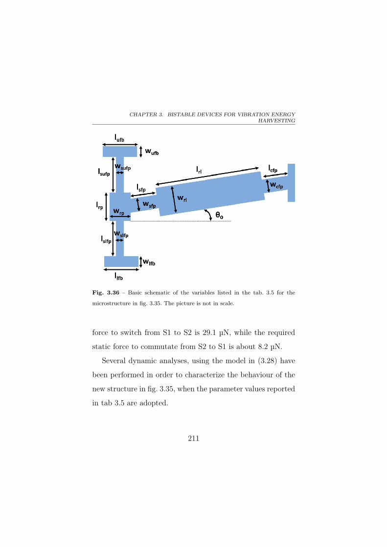
CHAPTER 3. BISTABLE DEVICES FOR VIBRATION ENERGYHARVESTING
Fig. 3.36 – Basic schematic of the variables listed in the tab. 3.5 for the
microstructure in fig. 3.35. The picture is not in scale.
force to switch from S1 to S2 is 29.1 µN, while the required
static force to commutate from S2 to S1 is about 8.2 µN.
Several dynamic analyses, using the model in (3.28) have
been performed in order to characterize the behaviour of the
new structure in fig. 3.35, when the parameter values reported
in tab 3.5 are adopted.
211
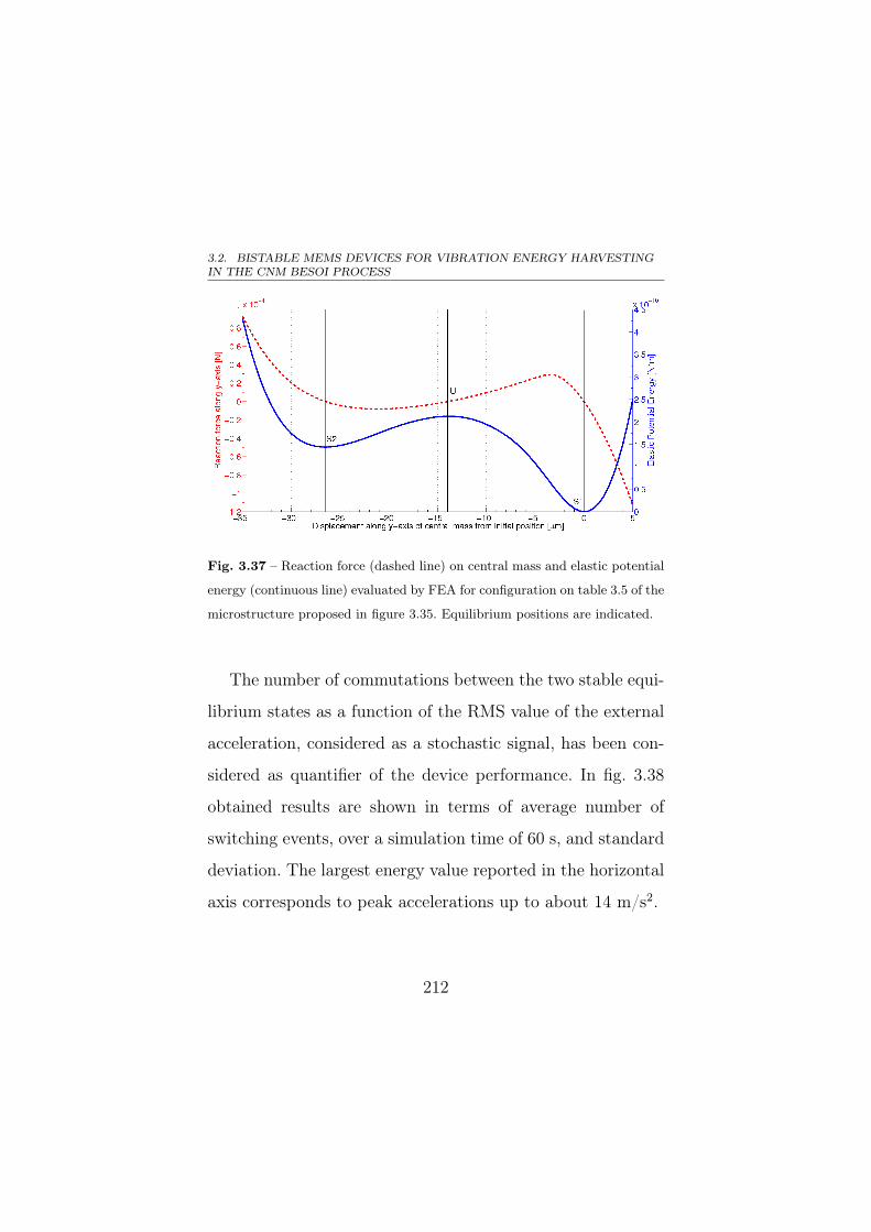
3.2. BISTABLE MEMS DEVICES FOR VIBRATION ENERGY HARVESTINGIN THE CNM BESOI PROCESS
Fig. 3.37 – Reaction force (dashed line) on central mass and elastic potential
energy (continuous line) evaluated by FEA for configuration on table 3.5 of the
microstructure proposed in figure 3.35. Equilibrium positions are indicated.
The number of commutations between the two stable equi-
librium states as a function of the RMS value of the external
acceleration, considered as a stochastic signal, has been con-
sidered as quantifier of the device performance. In fig. 3.38
obtained results are shown in terms of average number of
switching events, over a simulation time of 60 s, and standard
deviation. The largest energy value reported in the horizontal
axis corresponds to peak accelerations up to about 14 m/s2.
212
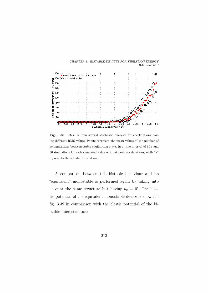
CHAPTER 3. BISTABLE DEVICES FOR VIBRATION ENERGYHARVESTING
Fig. 3.38 – Results from several stochastic analyses for accelerations hav-
ing different RMS values. Points represent the mean values of the number of
commutations between stable equilibrium states in a time interval of 60 s and
30 simulations for each simulated value of input peak accelerations; while “x”
represents the standard deviation.
A comparison between this bistable behaviour and its
“equivalent” monostable is performed again by taking into
account the same structure but having θ0 = 0°. The elas-
tic potential of the equivalent monostable device is shown in
fig. 3.39 in comparison with the elastic potential of the bi-
stable microstructure.
213
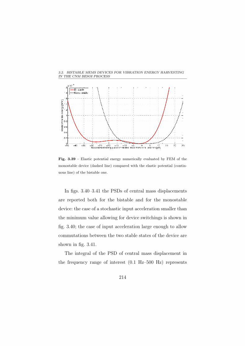
3.2. BISTABLE MEMS DEVICES FOR VIBRATION ENERGY HARVESTINGIN THE CNM BESOI PROCESS
Fig. 3.39 – Elastic potential energy numerically evaluated by FEM of the
monostable device (dashed line) compared with the elastic potential (contin-
uous line) of the bistable one.
In figs. 3.40–3.41 the PSDs of central mass displacements
are reported both for the bistable and for the monostable
device: the case of a stochastic input acceleration smaller than
the minimum value allowing for device switchings is shown in
fig. 3.40; the case of input acceleration large enough to allow
commutations between the two stable states of the device are
shown in fig. 3.41.
The integral of the PSD of central mass displacement in
the frequency range of interest (0.1 Hz–500 Hz) represents
214
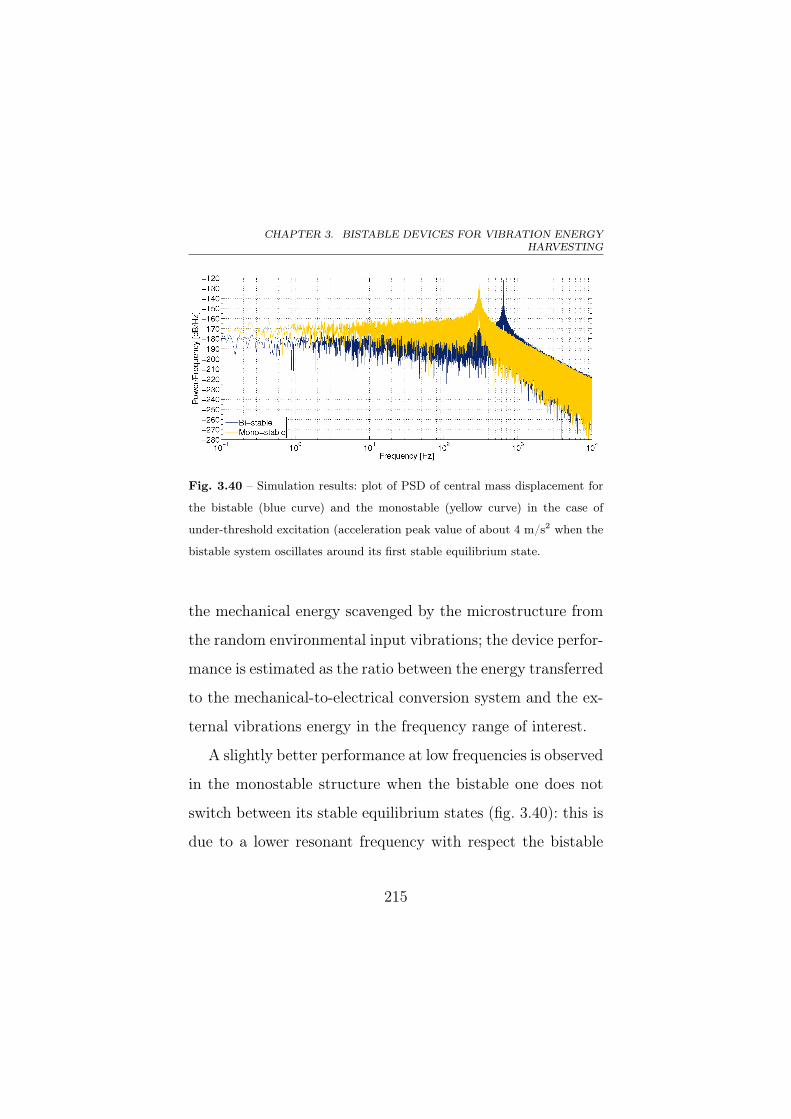
CHAPTER 3. BISTABLE DEVICES FOR VIBRATION ENERGYHARVESTING
Fig. 3.40 – Simulation results: plot of PSD of central mass displacement for
the bistable (blue curve) and the monostable (yellow curve) in the case of
under-threshold excitation (acceleration peak value of about 4 m/s2 when the
bistable system oscillates around its first stable equilibrium state.
the mechanical energy scavenged by the microstructure from
the random environmental input vibrations; the device perfor-
mance is estimated as the ratio between the energy transferred
to the mechanical-to-electrical conversion system and the ex-
ternal vibrations energy in the frequency range of interest.
A slightly better performance at low frequencies is observed
in the monostable structure when the bistable one does not
switch between its stable equilibrium states (fig. 3.40): this is
due to a lower resonant frequency with respect the bistable
215

3.2. BISTABLE MEMS DEVICES FOR VIBRATION ENERGY HARVESTINGIN THE CNM BESOI PROCESS
Fig. 3.41 – Simulation results: plot of PSD of central mass displacement for
the bistable (blue curve) and the monostable (yellow curve) in the case of
underthreshold excitation (acceleration peak value of about 13 m/s2 when the
bistable system oscillates around its first stable equilibrium state.
one. When the bistable structure begins to switch between its
stable equilibrium states, its behaviour is considerably more
efficient than the monostable one (fig. 3.41).
In fig. 3.42 the total energy gathered is plotted, for both the
monostable and the bistable structures, as a function of the
RMS value of input acceleration. The energy is evaluated as
the normalized PSD integral, in the frequency range of 0.1 Hz–
500 Hz of the central mass displacement. Normalization is
216
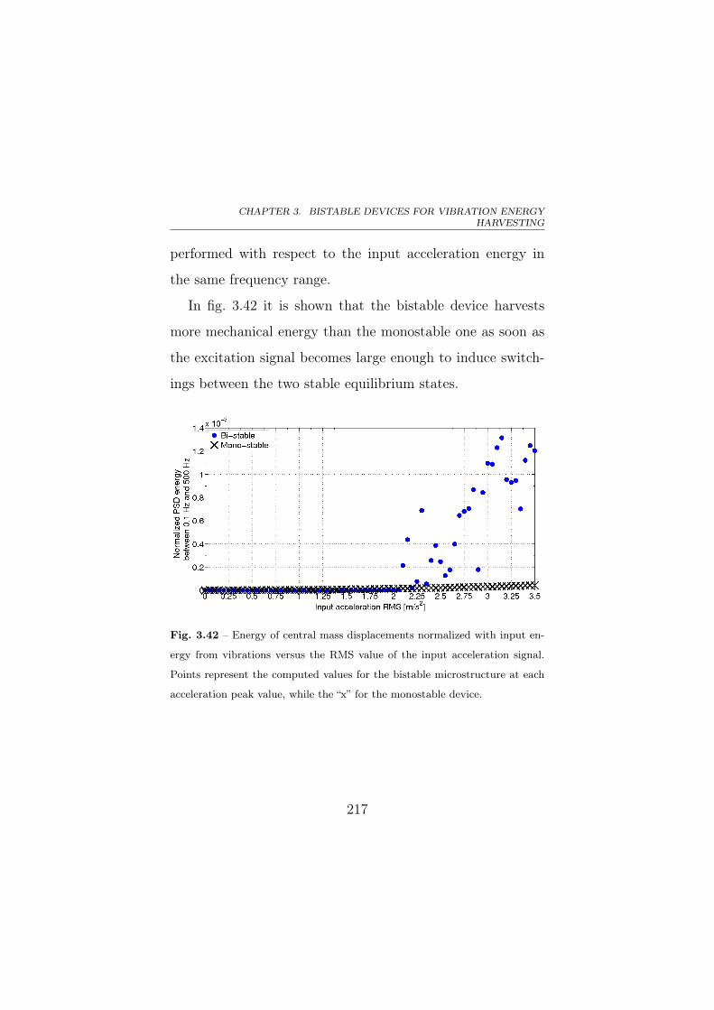
CHAPTER 3. BISTABLE DEVICES FOR VIBRATION ENERGYHARVESTING
performed with respect to the input acceleration energy in
the same frequency range.
In fig. 3.42 it is shown that the bistable device harvests
more mechanical energy than the monostable one as soon as
the excitation signal becomes large enough to induce switch-
ings between the two stable equilibrium states.
Fig. 3.42 – Energy of central mass displacements normalized with input en-
ergy from vibrations versus the RMS value of the input acceleration signal.
Points represent the computed values for the bistable microstructure at each
acceleration peak value, while the “x” for the monostable device.
217
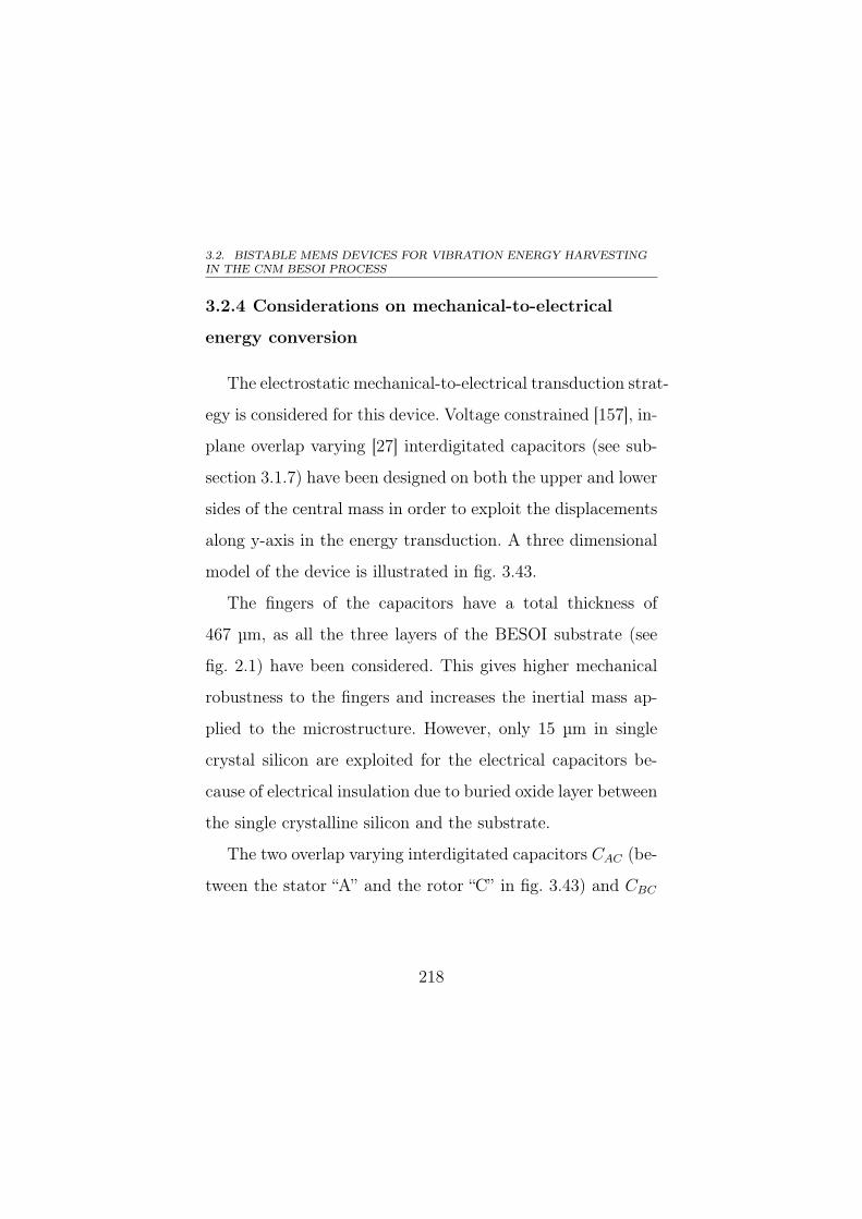
3.2. BISTABLE MEMS DEVICES FOR VIBRATION ENERGY HARVESTINGIN THE CNM BESOI PROCESS
3.2.4 Considerations on mechanical-to-electrical
energy conversion
The electrostatic mechanical-to-electrical transduction strat-
egy is considered for this device. Voltage constrained [157], in-
plane overlap varying [27] interdigitated capacitors (see sub-
section 3.1.7) have been designed on both the upper and lower
sides of the central mass in order to exploit the displacements
along y-axis in the energy transduction. A three dimensional
model of the device is illustrated in fig. 3.43.
The fingers of the capacitors have a total thickness of
467 µm, as all the three layers of the BESOI substrate (see
fig. 2.1) have been considered. This gives higher mechanical
robustness to the fingers and increases the inertial mass ap-
plied to the microstructure. However, only 15 µm in single
crystal silicon are exploited for the electrical capacitors be-
cause of electrical insulation due to buried oxide layer between
the single crystalline silicon and the substrate.
The two overlap varying interdigitated capacitors CAC (be-
tween the stator “A” and the rotor “C” in fig. 3.43) and CBC
218

CHAPTER 3. BISTABLE DEVICES FOR VIBRATION ENERGYHARVESTING
Fig. 3.43 – Three dimensional model of the device incorporating the mi-
crostructure in fig. 3.35 and the mechanical-to-electrical transduction mecha-
nism. The letters “A”, “B” and “C” indicate the pads for the electrical connec-
tion of the plates of the interdigitated capacitors.
(between the stator “B” the rotor “C” in fig. 3.43) are defined
in (3.30) and in (3.31) [22], with reference to (3.10).
CAC(y) = 2Nfε0tf
(lf0 − y
)g
(3.30)
CBC(y) = 2Nfε0tf
(lf0 + y
)g
(3.31)
219
3.2. BISTABLE MEMS DEVICES FOR VIBRATION ENERGY HARVESTINGIN THE CNM BESOI PROCESS
where Nf is the number of fingers (on the rotor side of
the capacitor), ε0 is the electrical permittivity of air, tf is the
thickness of the electrical layer in the capacitor, g is the air
gap, lf0 is the length of the overlap between two fingers facing
each other and y is the displacement of the central mass along
the y-axis from its initial position.
Taking into account the applied mechanical-to-electrical
conversion system(see subsection 3.1.7), the model in (3.26))
modifies [202] in (3.32), according to (3.13).
my + c∗y + be(y) + Ψ(y) = −maext (3.32)
The parameter c∗ in (3.32) represents the mechanical damp-
ing caused predominantly by the slide film effect in the inter-
digitated capacitors and is stated by (3.33) [53].
c∗ = 4Nfηtf lf0
g(3.33)
where η is the dynamic viscosity of air (η = 18 µPa·s).
The term be is the electrical damping that models the effect
of the electrical polarization of the two interdigitated capaci-
220
CHAPTER 3. BISTABLE DEVICES FOR VIBRATION ENERGYHARVESTING
tors CAC(y) and CBC(y) on the mass movement and is defined
by (3.34) [202], according to (3.14).
be(y) =ε0Nf tfg
VAC2 − ε0Nf tf
gVBC
2 (3.34)
where the terms VAC and VBC are respectively the polar-
ization voltages of the capacitors CAC and CBC . The signs
in (3.14) indicate the directions of the damping forces from
the two capacitors (when each of them is polarized) that are
opposite to the direction of the motion of the central mass.
According to (3.30)–(3.31) and considering the bistable dy-
namic operation of the proposed device, if any overshoots in
the displacement of the central mass are neglected, the capac-
itance CAC presents its maximum value in S1 while CBC its
minimum; analogously, in S2, CAC is at its minimum while
CBC at its maximum.
On the basis of the operating cycle of voltage constrained
electrostatic mechanical-to-electrical transduction systems [162],
the voltage VAC is equal to the applied voltage Vin only when
the central mass goes from S1 to S2 and in the other cases
VAC is equal to 0 V, while VBC is equal to Vin when the cen-
221
3.2. BISTABLE MEMS DEVICES FOR VIBRATION ENERGY HARVESTINGIN THE CNM BESOI PROCESS
tral mass comes from S2 to S1 and in the other cases VBC is
equal to 0 V. The energy harvested respectively by the capac-
itor CAC in each cycle of commutation from S1 to S2 and by
the capacitor CBC in each cycle of commutation from S2 to
S1 are expressed by EAC and EBC in (3.35) and (3.36) [157],
according to (3.15).
EAC =1
2
(CAC(S1)− CAC(S2)
)Vin
2 (3.35)
EBC =1
2
(CBC(S2)− CBC(S1)
)Vin
2 (3.36)
If a time series of length ts is observed, an estimation of
the power harvested P by the whole system during the obser-
vation time ts can be done by counting the number of com-
mutations from S1 to S2, N12, and from S2 to S1, N21, and
taking into account (3.35)–(3.36) in (3.37) [157].
P =N12
tsEAC +
N21
tsEBC (3.37)
The computed values of the parameters of the interdigi-
tated fingers for the mechanical-to-electrical energy conver-
sion are listed in the tab. 3.6. The choice of these values is
222

CHAPTER 3. BISTABLE DEVICES FOR VIBRATION ENERGYHARVESTING
motivated by the need to ensure an adequate extraction of en-
ergy without affecting the robustness of the fingers and taking
into account the movements of the structure between the two
stable equilibrium states.
Table 3.6 – Parameters of the adopted mechanical-to-electrical transduction
mechanism for the device in fig. 3.43. Values are equal for both the capacitances
CAC and CBC .
Variable Value Description
Nf 29 Number of fingers on rotor
lf 150 µm Total length of each finger
lf0 75 µm Initial overlap length between two fingers
t 467 µm Mechanical thickness of each finger
tf 15 µm Thickness of the conductive layer
wf 5 µm Width of each finger
g 15 µm Air gap between two fingers
A possible solution to increase the energy harvested in each
cycle of commutation EAC and EBC in (3.35)–(3.36) is to in-
crease the difference in the maximum and minimum values
of the capacitances CAC and CBC . This can be achieved by
exploiting also the thickness of the silicon substrate in the in-
223
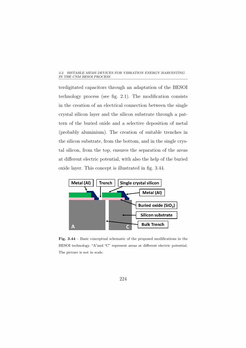
3.2. BISTABLE MEMS DEVICES FOR VIBRATION ENERGY HARVESTINGIN THE CNM BESOI PROCESS
terdigitated capacitors through an adaptation of the BESOI
technology process (see fig. 2.1). The modification consists
in the creation of an electrical connection between the single
crystal silicon layer and the silicon substrate through a pat-
tern of the buried oxide and a selective deposition of metal
(probably aluminium). The creation of suitable trenches in
the silicon substrate, from the bottom, and in the single crys-
tal silicon, from the top, ensures the separation of the areas
at different electric potential, with also the help of the buried
oxide layer. This concept is illustrated in fig. 3.44.
Fig. 3.44 – Basic conceptual schematic of the proposed modifications in the
BESOI technology. “A”and “C” represent areas at different electric potential.
The picture is not in scale.
224
CHAPTER 3. BISTABLE DEVICES FOR VIBRATION ENERGYHARVESTING
Thanks to this eventual modification in the technology pro-
cess, the thickness of the conductive layer on each finger tf
comes from 15 µm to 465 µm (see fig. 2.1). This increases
the values of the two capacitances CAC and CBC from (3.30)–
(3.31), the difference between their maximum and minimum
values and, from (3.35)–(3.36), the amount of the electrical
harvested energy.
In order to estimate the power harvested by the whole sys-
tem from (3.37) as a benchmark of the proposed concept,
the same microstructures studied in subsection 3.2.2 (the bi-
stable microstructure and its “equivalent” monostable one)
with the same mechanical-to-electrical transducers have been
compared in simulations for several accelerations having dif-
ferent associated energy, random dynamics and a spectrum
wide about 500 Hz [202]. This range of low frequency vibra-
tions is the most critical to be explored in order to exploit
the benefits of the proposed bistable device with respect to
linear or monostable systems. Models in (3.32)–(3.37) have
been taken into account and parasitic effects are neglected.
225
3.2. BISTABLE MEMS DEVICES FOR VIBRATION ENERGY HARVESTINGIN THE CNM BESOI PROCESS
As the displacements of the central mass in the monos-
table structure do not always have the same amplitude (ne-
glecting any overshoots) when the device is forced by noisy
vibrations, there are no fixed maximum and minimum val-
ues for the capacitances CAC and CBC in the system dynam-
ics, differently from the bistable device. In order to adopt the
models in (3.32)–(3.37) and the same strategies of the bistable
device in the polarization of the capacitances CAC and CBC ,
two values of displacements tl to th have been imposed as
thresholds to control the polarization and the depolarization
of the transduction capacitors (in the same way of the po-
sitions S1 and S2 in bistable device). So, in the monostable
case, CAC is polarized by Vin when the central mass comes
from the higher threshold th to the lower threshold tl, analo-
gously CBC is polarized when the system goes from tl to th.
Three different pairs of thresholds have been analyzed in the
comparisons with the bistable device: th =1 5 µm and tl = -
5 µm, th = 10 µm and tl = -10 µm and, finally, th = 13.35 µm
and tl = -13.35 µm. The last pair (th = 13.35 µm and tl = -
226

CHAPTER 3. BISTABLE DEVICES FOR VIBRATION ENERGYHARVESTING
13.35 µm) presents the same length of displacements between
the two equilibrium stable states of the bistable device.
Results are presented as the mean values over 30 time series
of 100 s each of the power harvested evaluated through (3.37)
for different RMS input accelerations. Figure 3.45 summarizes
the results for Vin = 30 V.
Fig. 3.45 – Power harvested at several RMS value of input acceleration for
the bistable device and its “equivalent” monostable one. A polarization voltage
of 30 V and the parameters for the transduction mechanism in the tab. 3.6,
with tf = 465 µm, are considered.
227
3.3. BISTABLE MEMS DEVICES FOR VIBRATION ENERGY HARVESTINGIN THE STMICROELECTRONICS THELMA® PROCESS
Results in fig. 3.45 confirm the improvement in perfor-
mance of the bistable device over the monostable one as soon
as the input acceleration is able to put it in commutation
between its two stable equilibrium states.
3.3 Bistable MEMS devices for vibration
energy harvesting in the STMicroelectronics
ThELMA® process
The same methodology followed in the section 3.2 for de-
signing a bistable MEMS harvester exploiting electrostatic
transduction has been adopted in this section to design a
MEMS device for vibration energy harvesting in the STMi-
croelectronics ThELMA® process.
As discussed in the subsection 2.1.4, ThELMA® technol-
ogy is a surface micromachining process that ensures smaller
structural dimensions than bulk micromachining processes,
such as BESOI process. Differences in device sizes and perfor-
mances will be evidenced in the following subsections.
228
CHAPTER 3. BISTABLE DEVICES FOR VIBRATION ENERGYHARVESTING
3.3.1 The mechanical microstructure
In order to reduce the overall dimensions of the struc-
ture and its wafer occupancy, although the shape of flexural
beams is the same as the ones of the BESOI device in subsec-
tion 3.2.3, the position of the four flexural beams holding the
central mass has been changed (with respect to the BESOI
device in subsection 3.2.3) to get a more compact microstruc-
ture.
An image of the concept of the studied structure is illus-
trated in fig. 3.46 and the geometry of the flexural beams is
reported in fig. 3.47.
The 22 µm thick epitaxial polysilicon layer has been ex-
ploited for the device structure.
3.3.2 FEM analyses of the microstructure
The proposed microstructure has been simulated through
FEM analyses on ANSYS® platform by adopting the same
methodology applied to the structure in subsection 3.2.2. The
aim is to properly design structure geometrical parameters
in order to achieve bistable behaviour with a proper poten-
229
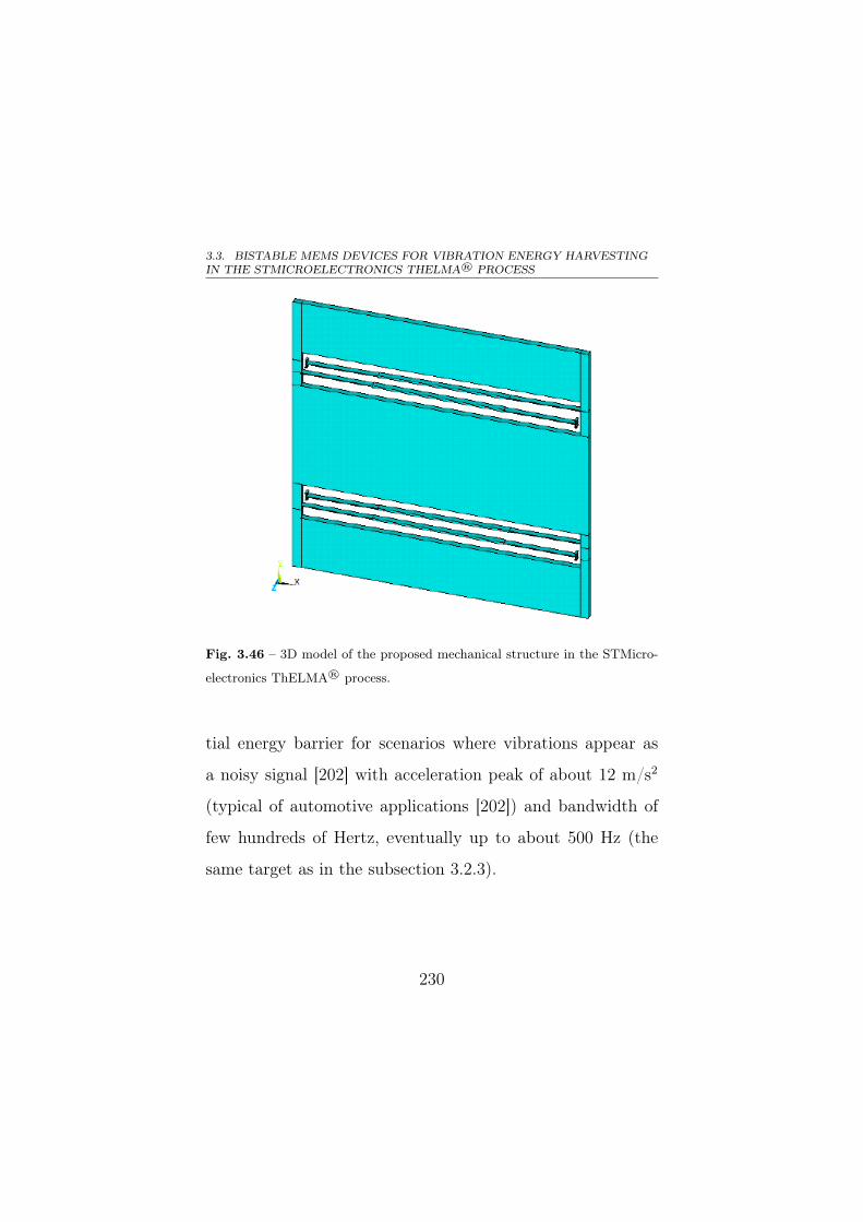
3.3. BISTABLE MEMS DEVICES FOR VIBRATION ENERGY HARVESTINGIN THE STMICROELECTRONICS THELMA® PROCESS
Fig. 3.46 – 3D model of the proposed mechanical structure in the STMicro-
electronics ThELMA® process.
tial energy barrier for scenarios where vibrations appear as
a noisy signal [202] with acceleration peak of about 12 m/s2
(typical of automotive applications [202]) and bandwidth of
few hundreds of Hertz, eventually up to about 500 Hz (the
same target as in the subsection 3.2.3).
230
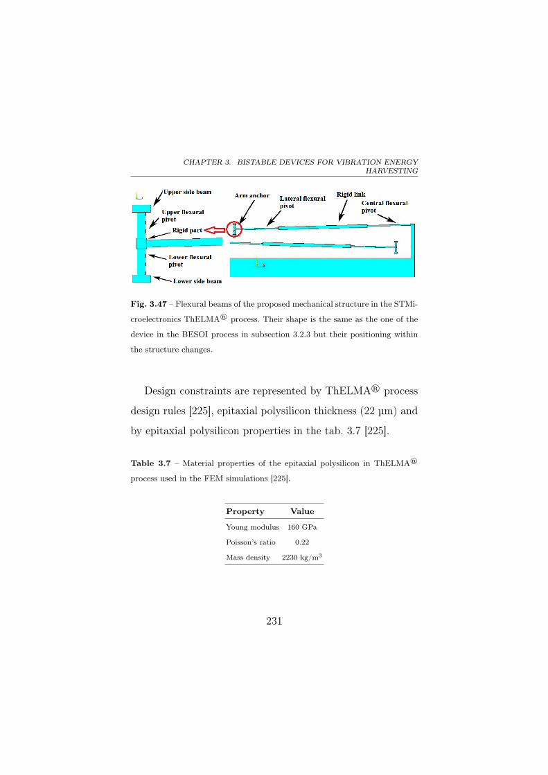
CHAPTER 3. BISTABLE DEVICES FOR VIBRATION ENERGYHARVESTING
Fig. 3.47 – Flexural beams of the proposed mechanical structure in the STMi-
croelectronics ThELMA® process. Their shape is the same as the one of the
device in the BESOI process in subsection 3.2.3 but their positioning within
the structure changes.
Design constraints are represented by ThELMA® process
design rules [225], epitaxial polysilicon thickness (22 µm) and
by epitaxial polysilicon properties in the tab. 3.7 [225].
Table 3.7 – Material properties of the epitaxial polysilicon in ThELMA®
process used in the FEM simulations [225].
Property Value
Young modulus 160 GPa
Poisson’s ratio 0.22
Mass density 2230 kg/m3
231
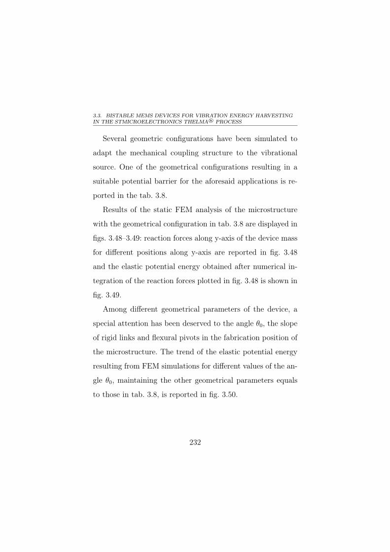
3.3. BISTABLE MEMS DEVICES FOR VIBRATION ENERGY HARVESTINGIN THE STMICROELECTRONICS THELMA® PROCESS
Several geometric configurations have been simulated to
adapt the mechanical coupling structure to the vibrational
source. One of the geometrical configurations resulting in a
suitable potential barrier for the aforesaid applications is re-
ported in the tab. 3.8.
Results of the static FEM analysis of the microstructure
with the geometrical configuration in tab. 3.8 are displayed in
figs. 3.48–3.49: reaction forces along y-axis of the device mass
for different positions along y-axis are reported in fig. 3.48
and the elastic potential energy obtained after numerical in-
tegration of the reaction forces plotted in fig. 3.48 is shown in
fig. 3.49.
Among different geometrical parameters of the device, a
special attention has been deserved to the angle θ0, the slope
of rigid links and flexural pivots in the fabrication position of
the microstructure. The trend of the elastic potential energy
resulting from FEM simulations for different values of the an-
gle θ0, maintaining the other geometrical parameters equals
to those in tab. 3.8, is reported in fig. 3.50.
232

CHAPTER 3. BISTABLE DEVICES FOR VIBRATION ENERGYHARVESTING
Table 3.8 – Geometric parameters of the microstructure in fig. 3.46. The
microstructure is symmetric along y-axis. A basic schematic of the variables
listed is shown in fig. 3.36.
Variable Value Description
θ0 1.5° Slope of rigid links and flexural pivots
lsfp 110 µm Length of side flexural pivots
lrl 220 µm Length of rigid links
lcfp 110 µm Length of central flexural pivots
lrp 7 µm Length of rigid parts
lsufp 150 µm Length of side upper flexural pivots
lslfp 150 µm Length of side lower flexural pivots
lufb 150 µm Length of upper fixed beams
llfb 150 µm Length of lower fixed beams
wsfp 10 µm Width of side flexural pivots
wrl 7 µm Width of rigid links
wcfp 2.8 µm Width of central flexural pivots
wrp 7 µm Width of rigid parts
wsufp 4 µm Width of side upper flexural pivots
wslfp 4 µm Width of side lower flexural pivots
wufb 4 µm Width of upper fixed beams
wlfb 4 µm Width of lower fixed beams
t 22 µm Thickness of the entire structure
lm 1100 µm Length of the device mass
wm 500 µm Width of the device mass
233
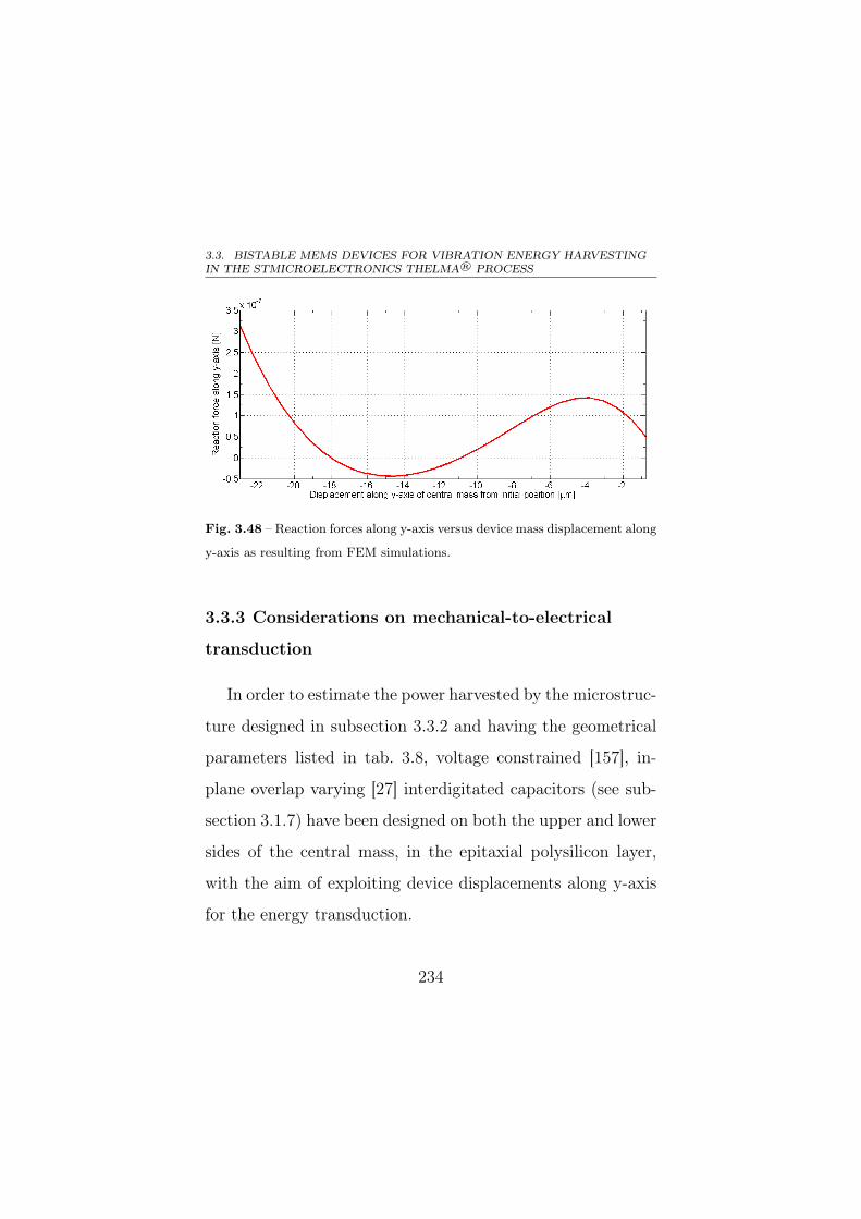
3.3. BISTABLE MEMS DEVICES FOR VIBRATION ENERGY HARVESTINGIN THE STMICROELECTRONICS THELMA® PROCESS
Fig. 3.48 – Reaction forces along y-axis versus device mass displacement along
y-axis as resulting from FEM simulations.
3.3.3 Considerations on mechanical-to-electrical
transduction
In order to estimate the power harvested by the microstruc-
ture designed in subsection 3.3.2 and having the geometrical
parameters listed in tab. 3.8, voltage constrained [157], in-
plane overlap varying [27] interdigitated capacitors (see sub-
section 3.1.7) have been designed on both the upper and lower
sides of the central mass, in the epitaxial polysilicon layer,
with the aim of exploiting device displacements along y-axis
for the energy transduction.
234
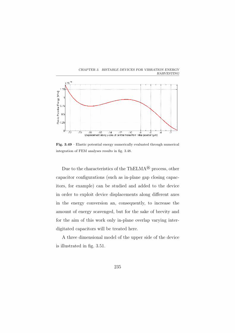
CHAPTER 3. BISTABLE DEVICES FOR VIBRATION ENERGYHARVESTING
Fig. 3.49 – Elastic potential energy numerically evaluated through numerical
integration of FEM analyses results in fig. 3.48.
Due to the characteristics of the ThELMA® process, other
capacitor configurations (such as in-plane gap closing capac-
itors, for example) can be studied and added to the device
in order to exploit device displacements along different axes
in the energy conversion an, consequently, to increase the
amount of energy scavenged, but for the sake of brevity and
for the aim of this work only in-plane overlap varying inter-
digitated capacitors will be treated here.
A three dimensional model of the upper side of the device
is illustrated in fig. 3.51.
235
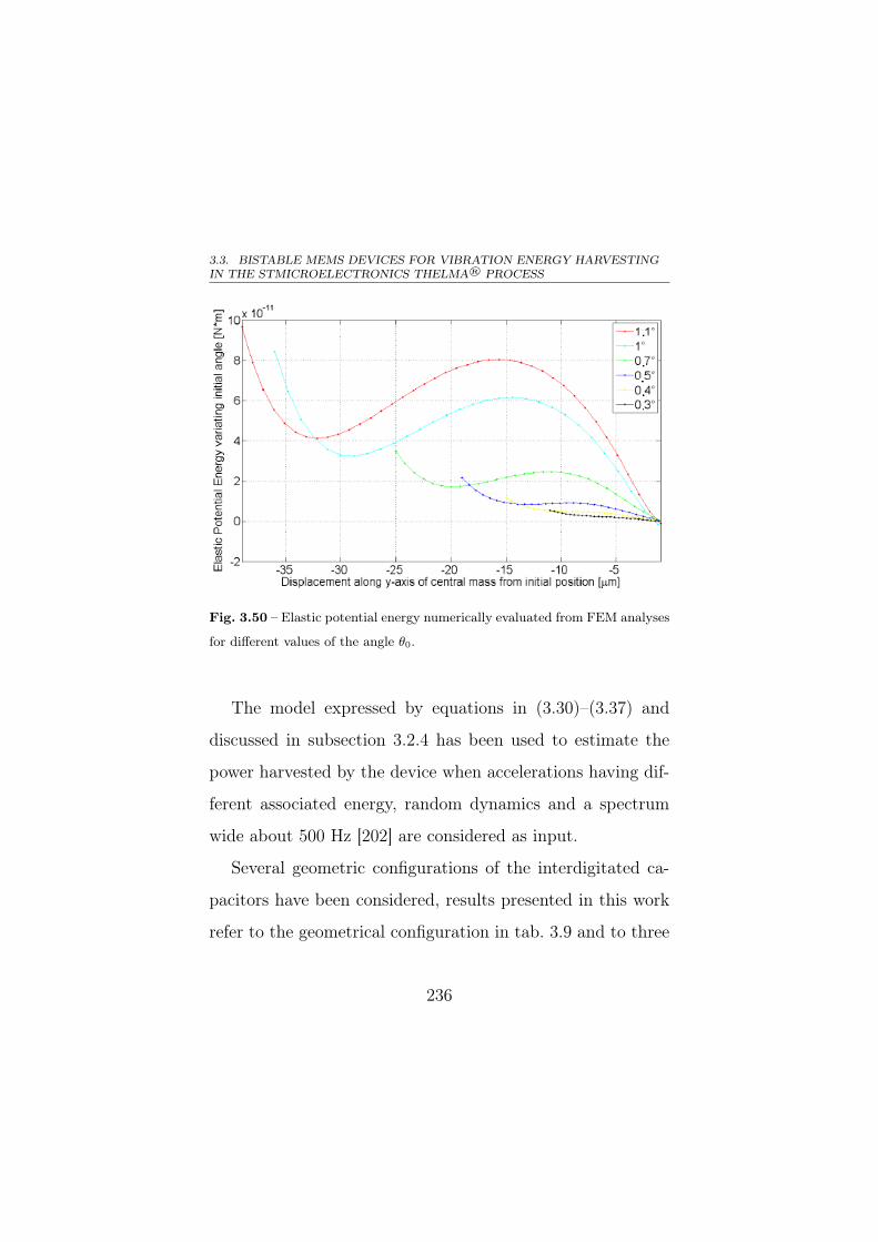
3.3. BISTABLE MEMS DEVICES FOR VIBRATION ENERGY HARVESTINGIN THE STMICROELECTRONICS THELMA® PROCESS
Fig. 3.50 – Elastic potential energy numerically evaluated from FEM analyses
for different values of the angle θ0.
The model expressed by equations in (3.30)–(3.37) and
discussed in subsection 3.2.4 has been used to estimate the
power harvested by the device when accelerations having dif-
ferent associated energy, random dynamics and a spectrum
wide about 500 Hz [202] are considered as input.
Several geometric configurations of the interdigitated ca-
pacitors have been considered, results presented in this work
refer to the geometrical configuration in tab. 3.9 and to three
236
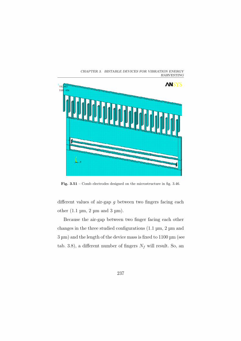
CHAPTER 3. BISTABLE DEVICES FOR VIBRATION ENERGYHARVESTING
Fig. 3.51 – Comb electrodes designed on the microstructure in fig. 3.46.
different values of air-gap g between two fingers facing each
other (1.1 µm, 2 µm and 3 µm).
Because the air-gap between two finger facing each other
changes in the three studied configurations (1.1 µm, 2 µm and
3 µm) and the length of the device mass is fixed to 1100 µm (see
tab. 3.8), a different number of fingers Nf will result. So, an
237

3.3. BISTABLE MEMS DEVICES FOR VIBRATION ENERGY HARVESTINGIN THE STMICROELECTRONICS THELMA® PROCESS
Table 3.9 – Parameters of the adopted mechanical-to-electrical transduction
mechanism for the device in fig. 3.51.
Variable Value Description
lf 40 µm Total length of each finger
lf0 15 µm Initial overlap length between two fingers
t 22 µm Mechanical thickness of each finger
wf 2.7 µm Width of each finger
air-gap of 1.1 µm leads to 141 fingers, 2 µm to 114 and 3 µm to
94.
The different air-gap and the different number of fingers
affect the mechanical damping c∗, according to (3.33), and
the amount of the capacitance variation, see (3.30)–(3.31).
The mean electrical power harvested by the system and the
mean number of commutations between stable equilibrium
states (over 30 simulations) have been evaluated for several
values of the polarization voltage Vin, for the three studied
configurations and for an input acceleration aext having an
RMS value of 7 m/s2 and a bandwidth of 500 Hz. Results are
reported in tab. 3.10 when the air-gap is 1.1 µm, in tab. 3.11
238

CHAPTER 3. BISTABLE DEVICES FOR VIBRATION ENERGYHARVESTING
when the air-gap is 2 µm and in tab. 3.12 when the air-gap is
3 µm.
Table 3.10 – Mean electrical power harvested by the system and mean number
of commutations between stable equilibrium states (over 30 simulations) for
several values of the polarization voltage Vin, when an air-gap of 1.1 µm and
an input acceleration aext having an RMS value of 7 m/s2 and a bandwidth
of 500 Hz are applied to the system.
Voltage Mean power harvested Mean number of commutations
1 V 64 pW 932
2 V 242 pW 867
3 V 446 pW 712
4 V 580 pW 519
5 V 600 pW 344
6 V 522 pW 208
7 V 483 pW 114
In order to show the improvement due to bistability in
the amount of harvested power, the power scavenged by the
designed bistable device (with capacitor fingers having an air-
gap of 3 µm) has been compared with its “equivalent” monos-
table (i.e. the device having the same geometrical parameters
as the bistable one except for the angle θ, which is equal to
239

3.3. BISTABLE MEMS DEVICES FOR VIBRATION ENERGY HARVESTINGIN THE STMICROELECTRONICS THELMA® PROCESS
Table 3.11 – Mean electrical power harvested by the system and mean number
of commutations between stable equilibrium states (over 30 simulations) for
several values of the polarization voltage Vin, when an air-gap of 2 µm and an
input acceleration aext having an RMS value of 7 m/s2 and a bandwidth of
500 Hz are applied to the system.
Voltage Mean power harvested Mean number of commutations
3 V 366 pW 1314
4 V 546 pW 1101
5 V 700 pW 902
6 V 802 pW 720
7 V 902 pW 601
8 V 828 pW 417
9 V 792 pW 315
10 V 764 pW 246
0°, thus causing a monostable behaviour), in the same way as
in subsection 3.2.4.
Results of one of these benchmarking simulations are re-
ported in fig. 3.52 for different values of the polarization volt-
age Vin, when an input acceleration aext having an RMS value
of 7 m/s2 and a bandwidth of 500 Hz has been considered.
As the displacements of the central mass in the monostable
structure do not always have the same amplitude (neglect-
240
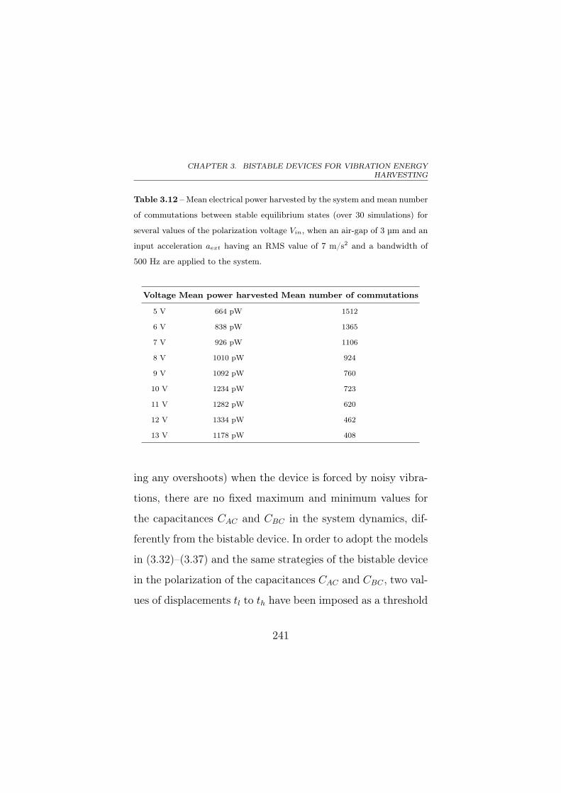
CHAPTER 3. BISTABLE DEVICES FOR VIBRATION ENERGYHARVESTING
Table 3.12 – Mean electrical power harvested by the system and mean number
of commutations between stable equilibrium states (over 30 simulations) for
several values of the polarization voltage Vin, when an air-gap of 3 µm and an
input acceleration aext having an RMS value of 7 m/s2 and a bandwidth of
500 Hz are applied to the system.
Voltage Mean power harvested Mean number of commutations
5 V 664 pW 1512
6 V 838 pW 1365
7 V 926 pW 1106
8 V 1010 pW 924
9 V 1092 pW 760
10 V 1234 pW 723
11 V 1282 pW 620
12 V 1334 pW 462
13 V 1178 pW 408
ing any overshoots) when the device is forced by noisy vibra-
tions, there are no fixed maximum and minimum values for
the capacitances CAC and CBC in the system dynamics, dif-
ferently from the bistable device. In order to adopt the models
in (3.32)–(3.37) and the same strategies of the bistable device
in the polarization of the capacitances CAC and CBC , two val-
ues of displacements tl to th have been imposed as a threshold
241
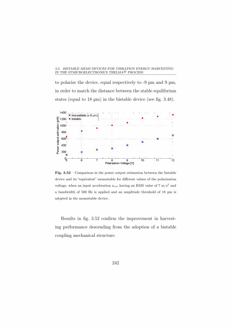
3.3. BISTABLE MEMS DEVICES FOR VIBRATION ENERGY HARVESTINGIN THE STMICROELECTRONICS THELMA® PROCESS
to polarize the device, equal respectively to -9 µm and 9 µm,
in order to match the distance between the stable equilibrium
states (equal to 18 µm) in the bistable device (see fig. 3.48).
Fig. 3.52 – Comparison in the power output estimation between the bistable
device and its “equivalent” monostable for different values of the polarization
voltage, when an input acceleration aext having an RMS value of 7 m/s2 and
a bandwidth of 500 Hz is applied and an amplitude threshold of 18 µm is
adopted in the monostable device.
Results in fig. 3.52 confirm the improvement in harvest-
ing performance descending from the adoption of a bistable
coupling mechanical structure.
242
CHAPTER 3. BISTABLE DEVICES FOR VIBRATION ENERGYHARVESTING
3.4 Bistable microstructure in the
MEMSCAPTM MetalMUMPs® process
In order to test the capabilities of the MetalMUMPs® pro-
cess from MEMSCAPTM (see subsection 2.1.2) in the im-
plementation of bistable microstructures, a MEMS structure,
previously microfabricated for thermal microsensors [18], has
been simulated and tested at the Nanotechlab of the Univer-
sity of Catania (Italy).
3.4.1 Cascaded triple bent-beam structure
The structure is based on a cascaded triple bent-beam sus-
pended architecture realized in the 20.5 µm thick electroplated
nickel layer of the MetalMUMPs® process [62].
The layout of the microstructure along with its geometric
specifications is shown in fig. 3.53; descriptions and values of
its geometric specifications are listed in tab. 3.13.
The 3D model of the device is illustrated in fig. 3.54.
243
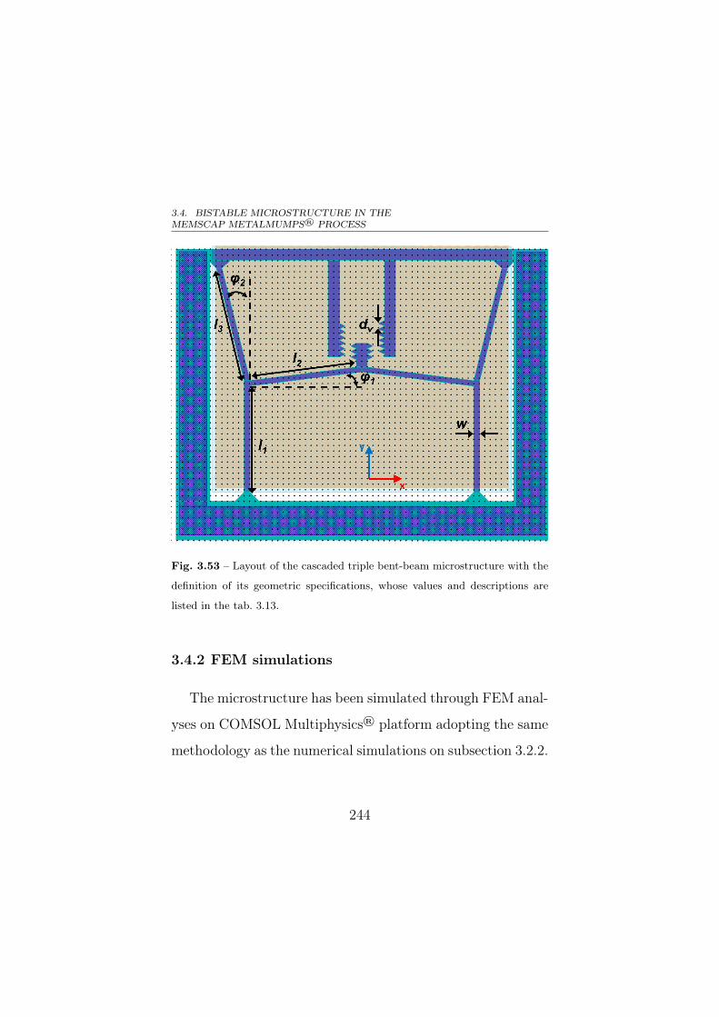
3.4. BISTABLE MICROSTRUCTURE IN THEMEMSCAP METALMUMPS® PROCESS
Fig. 3.53 – Layout of the cascaded triple bent-beam microstructure with the
definition of its geometric specifications, whose values and descriptions are
listed in the tab. 3.13.
3.4.2 FEM simulations
The microstructure has been simulated through FEM anal-
yses on COMSOL Multiphysics® platform adopting the same
methodology as the numerical simulations on subsection 3.2.2.
244
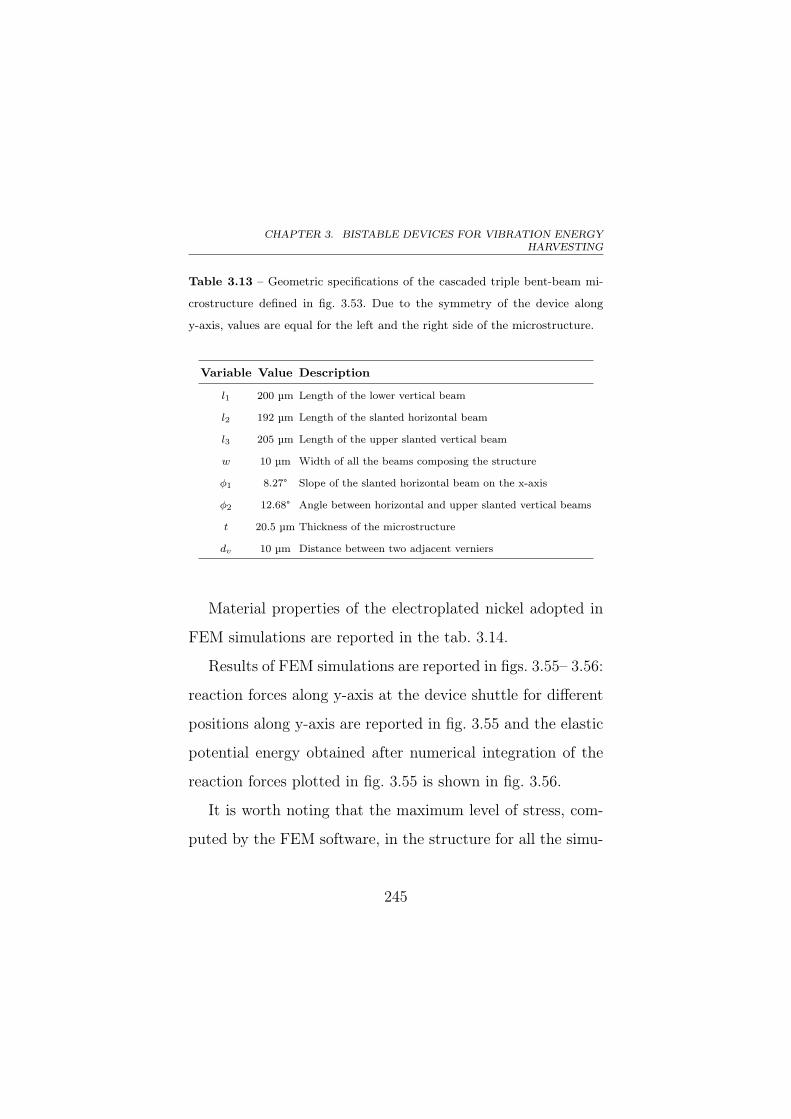
CHAPTER 3. BISTABLE DEVICES FOR VIBRATION ENERGYHARVESTING
Table 3.13 – Geometric specifications of the cascaded triple bent-beam mi-
crostructure defined in fig. 3.53. Due to the symmetry of the device along
y-axis, values are equal for the left and the right side of the microstructure.
Variable Value Description
l1 200 µm Length of the lower vertical beam
l2 192 µm Length of the slanted horizontal beam
l3 205 µm Length of the upper slanted vertical beam
w 10 µm Width of all the beams composing the structure
φ1 8.27° Slope of the slanted horizontal beam on the x-axis
φ2 12.68° Angle between horizontal and upper slanted vertical beams
t 20.5 µm Thickness of the microstructure
dv 10 µm Distance between two adjacent verniers
Material properties of the electroplated nickel adopted in
FEM simulations are reported in the tab. 3.14.
Results of FEM simulations are reported in figs. 3.55– 3.56:
reaction forces along y-axis at the device shuttle for different
positions along y-axis are reported in fig. 3.55 and the elastic
potential energy obtained after numerical integration of the
reaction forces plotted in fig. 3.55 is shown in fig. 3.56.
It is worth noting that the maximum level of stress, com-
puted by the FEM software, in the structure for all the simu-
245
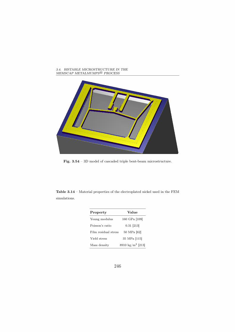
3.4. BISTABLE MICROSTRUCTURE IN THEMEMSCAP METALMUMPS® PROCESS
Fig. 3.54 – 3D model of cascaded triple bent-beam microstructure.
Table 3.14 – Material properties of the electroplated nickel used in the FEM
simulations.
Property Value
Young modulus 160 GPa [109]
Poisson’s ratio 0.31 [213]
Film residual stress 50 MPa [62]
Yield stress 35 MPa [115]
Mass density 8910 kg/m3 [213]
246
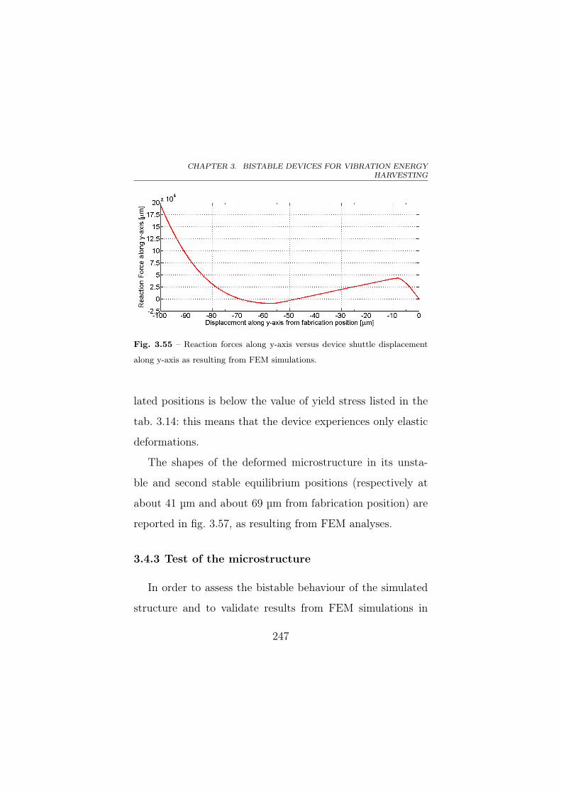
CHAPTER 3. BISTABLE DEVICES FOR VIBRATION ENERGYHARVESTING
Fig. 3.55 – Reaction forces along y-axis versus device shuttle displacement
along y-axis as resulting from FEM simulations.
lated positions is below the value of yield stress listed in the
tab. 3.14: this means that the device experiences only elastic
deformations.
The shapes of the deformed microstructure in its unsta-
ble and second stable equilibrium positions (respectively at
about 41 µm and about 69 µm from fabrication position) are
reported in fig. 3.57, as resulting from FEM analyses.
3.4.3 Test of the microstructure
In order to assess the bistable behaviour of the simulated
structure and to validate results from FEM simulations in
247
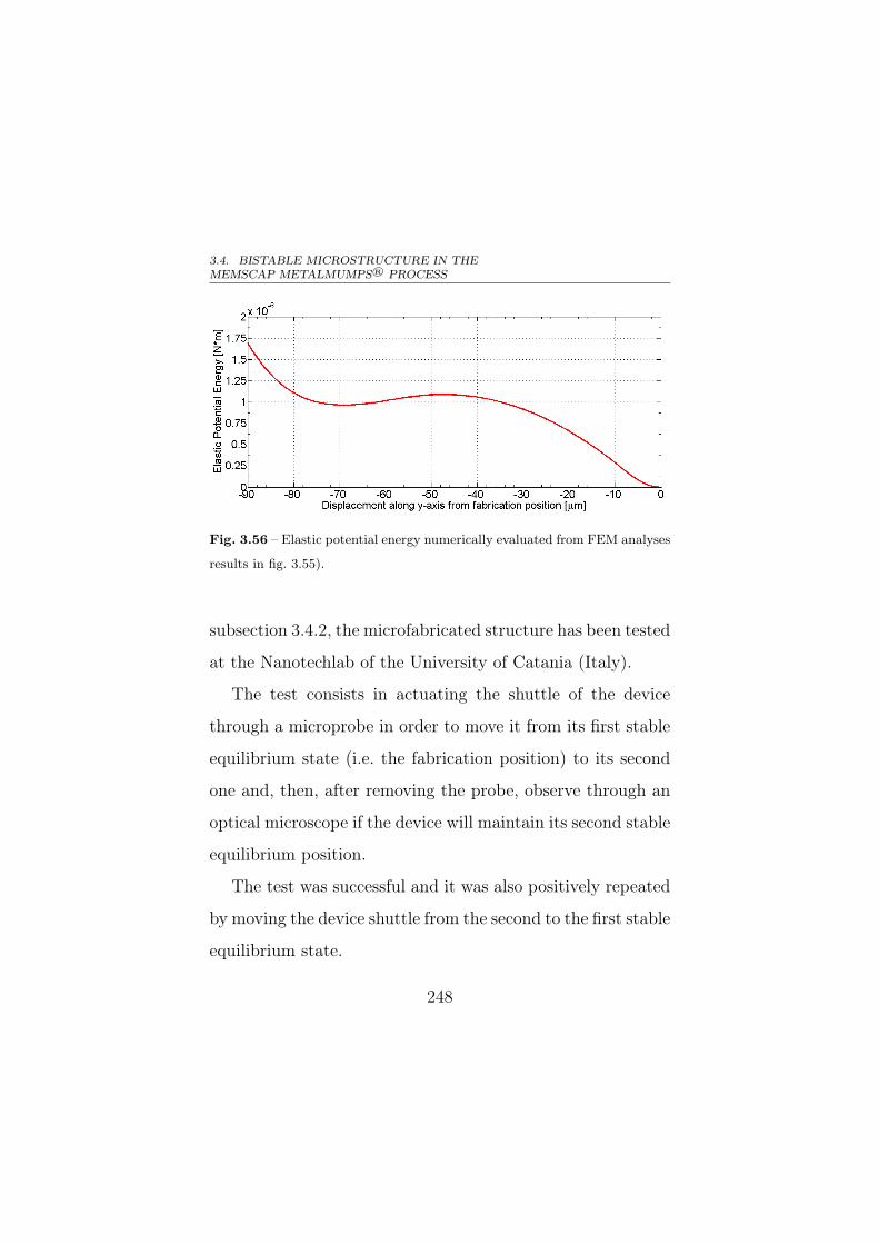
3.4. BISTABLE MICROSTRUCTURE IN THEMEMSCAP METALMUMPS® PROCESS
Fig. 3.56 – Elastic potential energy numerically evaluated from FEM analyses
results in fig. 3.55).
subsection 3.4.2, the microfabricated structure has been tested
at the Nanotechlab of the University of Catania (Italy).
The test consists in actuating the shuttle of the device
through a microprobe in order to move it from its first stable
equilibrium state (i.e. the fabrication position) to its second
one and, then, after removing the probe, observe through an
optical microscope if the device will maintain its second stable
equilibrium position.
The test was successful and it was also positively repeated
by moving the device shuttle from the second to the first stable
equilibrium state.
248
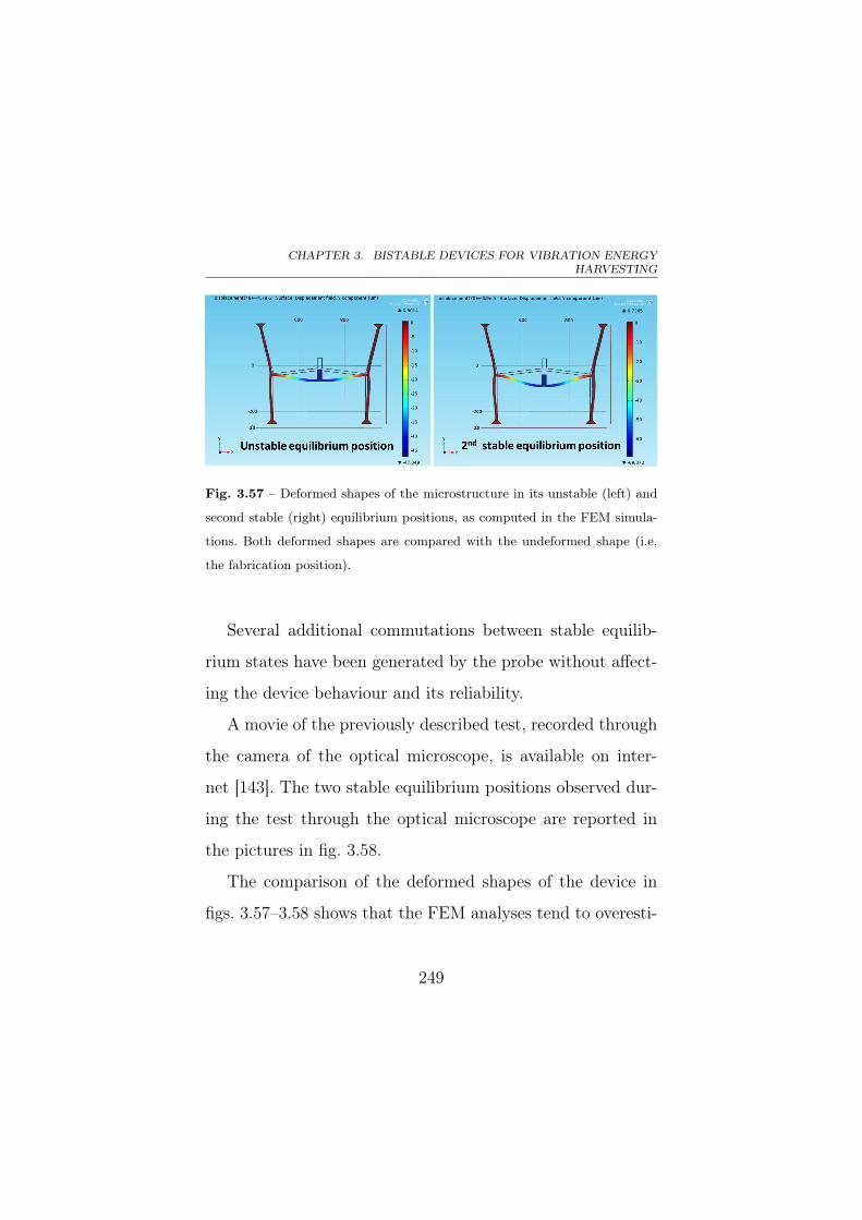
CHAPTER 3. BISTABLE DEVICES FOR VIBRATION ENERGYHARVESTING
Fig. 3.57 – Deformed shapes of the microstructure in its unstable (left) and
second stable (right) equilibrium positions, as computed in the FEM simula-
tions. Both deformed shapes are compared with the undeformed shape (i.e.
the fabrication position).
Several additional commutations between stable equilib-
rium states have been generated by the probe without affect-
ing the device behaviour and its reliability.
A movie of the previously described test, recorded through
the camera of the optical microscope, is available on inter-
net [143]. The two stable equilibrium positions observed dur-
ing the test through the optical microscope are reported in
the pictures in fig. 3.58.
The comparison of the deformed shapes of the device in
figs. 3.57–3.58 shows that the FEM analyses tend to overesti-
249
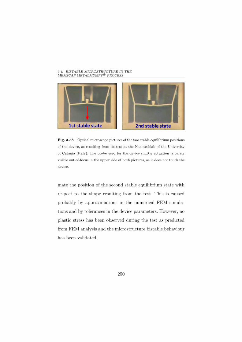
3.4. BISTABLE MICROSTRUCTURE IN THEMEMSCAP METALMUMPS® PROCESS
Fig. 3.58 – Optical microscope pictures of the two stable equilibrium positions
of the device, as resulting from its test at the Nanotechlab of the University
of Catania (Italy). The probe used for the device shuttle actuation is barely
visible out-of-focus in the upper side of both pictures, as it does not touch the
device.
mate the position of the second stable equilibrium state with
respect to the shape resulting from the test. This is caused
probably by approximations in the numerical FEM simula-
tions and by tolerances in the device parameters. However, no
plastic stress has been observed during the test as predicted
from FEM analysis and the microstructure bistable behaviour
has been validated.
250
CHAPTER 3. BISTABLE DEVICES FOR VIBRATION ENERGYHARVESTING
Results exposed in this section reveals the suitability of
the MetalMUMPs® process from MEMSCAPTM to develop
bistable structures for energy harvesting.
3.5 Bistable devices for vibration energy
harvesting in in direct printing technology
Direct printing technology process at the Sensor Lab of
the University of Catania (Italy), described in section 2.3,
has been exploited to develop a macroscale prototype of a
nonlinear piezoelectric energy harvester based on a bistable
snap-through buckled beam [4].
Buckled beams represent a strategy to obtain a bistable
structure by simply applying an axial stress (tensile or com-
pressive) or an axial loading or an axial compressive displace-
ment to a clamped-clamped beam respectively larger than
critical stress σcr defined in (3.38), critical axial load Pcr de-
fined in (3.39) and critical compressive displacement ∆cr de-
fined in (3.40) [199].
251
3.5. BISTABLE DEVICES FOR VIBRATION ENERGY HARVESTING IN INDIRECT PRINTING TECHNOLOGY
σcr =4π2EI
Al(3.38)
Pcr =4π2EI
l2(3.39)
∆cr =4π2I
Al(3.40)
where E is Young modulus, I is the cross section moment
of inertia (in the plane of bending), A is the cross section area,
and l is the in-plane length of the beam. The plane of buckling
will correspond to the smallest moment of inertia: in-plane if
Iyy < Izz and out-of-plane if Iyy > Izz, where Iyy = (1/12)w3t
(in-plane) and Izz = (1/12)wt3 (out-of-plane) for rectangular
cross-sections of out-of-plane thickness t and in-plane width
w.
There is a bifurcation in the buckling equations (i.e., the
direction of buckling of an ideal beam can be in either direc-
tion within the plane of buckling). Thus the beam has two
stable equilibrium positions, separated by an unstable equi-
librium position which corresponds to either a supercritically
stressed, unbuckled position or an intermediate elastica. The
beam may be actuated from one stable position and comes
to rest in the second stable position through the unstable
252
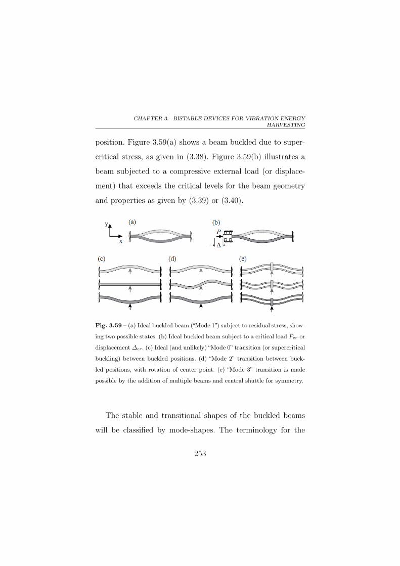
CHAPTER 3. BISTABLE DEVICES FOR VIBRATION ENERGYHARVESTING
position. Figure 3.59(a) shows a beam buckled due to super-
critical stress, as given in (3.38). Figure 3.59(b) illustrates a
beam subjected to a compressive external load (or displace-
ment) that exceeds the critical levels for the beam geometry
and properties as given by (3.39) or (3.40).
Fig. 3.59 – (a) Ideal buckled beam (“Mode 1”) subject to residual stress, show-
ing two possible states. (b) Ideal buckled beam subject to a critical load Pcr or
displacement ∆cr. (c) Ideal (and unlikely) “Mode 0” transition (or supercritical
buckling) between buckled positions. (d) “Mode 2” transition between buck-
led positions, with rotation of center point. (e) “Mode 3” transition is made
possible by the addition of multiple beams and central shuttle for symmetry.
The stable and transitional shapes of the buckled beams
will be classified by mode-shapes. The terminology for the
253

3.5. BISTABLE DEVICES FOR VIBRATION ENERGY HARVESTING IN INDIRECT PRINTING TECHNOLOGY
mode-shapes comes from the number of waveform modes cor-
responding to the number of times the beam crosses the x-axis
(not including the origin of the beam). The familiar buckled
shape, see fig. 3.59(a), is “Mode 1” buckling. The supercriti-
cally stressed transition corresponds to what will be termed
“Mode 0” buckling, or unbuckled deflection. The mode shape
of the intermediate elastica is “Mode 2”, see fig. 3.59(d). This
mode is undesirable for bistable switching applications as it
introduces rotations that may not be compatible with actua-
tion systems or contacts. This mode does however correspond
to the path of lowest potential energy between the stable po-
sitions (i.e. the path of least mechanical resistance). This is
because a “Mode 0” is highly unlikely and other mode-shapes
are always higher energy states. “Mode 2” transition can be
avoided by using multiple beams and a central shuttle, see
fig. 3.59(e), to provide stabilizing symmetry. The resulting
structure is stiffer than a single beam, due to the additional
beam and the “Mode 3” transitional mode-shape, but will be
less prone to rotational deformations.
254
CHAPTER 3. BISTABLE DEVICES FOR VIBRATION ENERGYHARVESTING
Bistable MEMS based on buckled beams have been pro-
posed utilizing beams buckled by residual stress [103, 239],
thermally induced stress [50], or by applying external loading
by on-chip actuation [207]. Another possible technique is to
fabricate the beam in one of the stable positions [192]. Al-
though not buckled in the initial (as fabricated) state, the
beam (or beams) can be designed to have a snap-through be-
haviour and they will however remain biased to the initial
position.
In this work the rapid prototyping of piezoelectric buckled
beams of centimeter size exploiting the benefits of the bistable
dynamics and assuring a wide bandwidth at low frequencies is
presented. Low cost strategies based on direct printing tech-
nologies are adopted in order to ensure the reducing of both
costs and time of realization.
3.5.1 The device and its working principle
The device consists of a PET substrate (“NoveleTM IJ-220
coated PET” from Novacentrix®, see fig. 2.30) having a thick-
ness of about 165 µm that implements a clamped-clamped
beam. The length l and the width w of the beam are design
255
3.5. BISTABLE DEVICES FOR VIBRATION ENERGY HARVESTING IN INDIRECT PRINTING TECHNOLOGY
parameters. On the top of this beam, a layer containing two
pads and two InterDigiTed Electrodes (IDT) has been realized
by inkjet printing of a conductive pattern of the silver nano-
particles solution ink “Metalon® JS-B15P” by Novacentrix
(see section 2.3) [172], through a cheap commercial EPSON®
piezo inkjet printer. IDT fingers width, length and thickness
are respectively about 200 µm, 5 mm and 250 nm, while the
track spacing is about 300 µm. The function of the IDT is the
electrical connection of the Lead Titanate Zirconate (PZT)
piezoelectric layer (from Piezokeramica APC 855 [20]) which
have a thickness of about 25 µm and is deposited above them
through screen printing at the Department of Information En-
gineering of the University of Brescia (Italy). After its depo-
sition, the PZT layer is cured at 100℃ for 10 minutes. A
clamping system allows for both the fixing of the beam ends
and the connection of the pads through proper sockets.
A picture of the realized prototype in its upper stable equi-
librium state and fixed by the clamping system is reported in
fig. 3.60 and diagram (not in scale) of the device layers com-
pared with a picture of the device is reported in fig. 3.61.
256
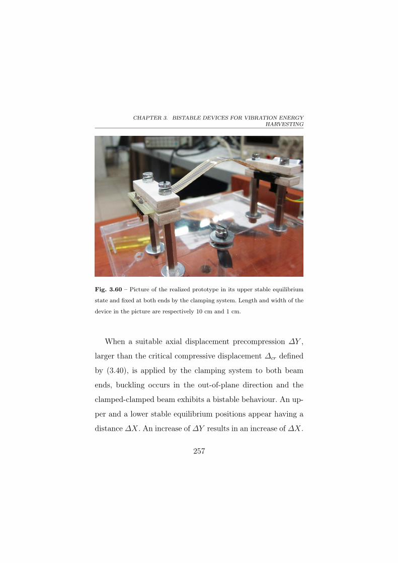
CHAPTER 3. BISTABLE DEVICES FOR VIBRATION ENERGYHARVESTING
Fig. 3.60 – Picture of the realized prototype in its upper stable equilibrium
state and fixed at both ends by the clamping system. Length and width of the
device in the picture are respectively 10 cm and 1 cm.
When a suitable axial displacement precompression ∆Y ,
larger than the critical compressive displacement ∆cr defined
by (3.40), is applied by the clamping system to both beam
ends, buckling occurs in the out-of-plane direction and the
clamped-clamped beam exhibits a bistable behaviour. An up-
per and a lower stable equilibrium positions appear having a
distance ∆X. An increase of ∆Y results in an increase of ∆X.
257
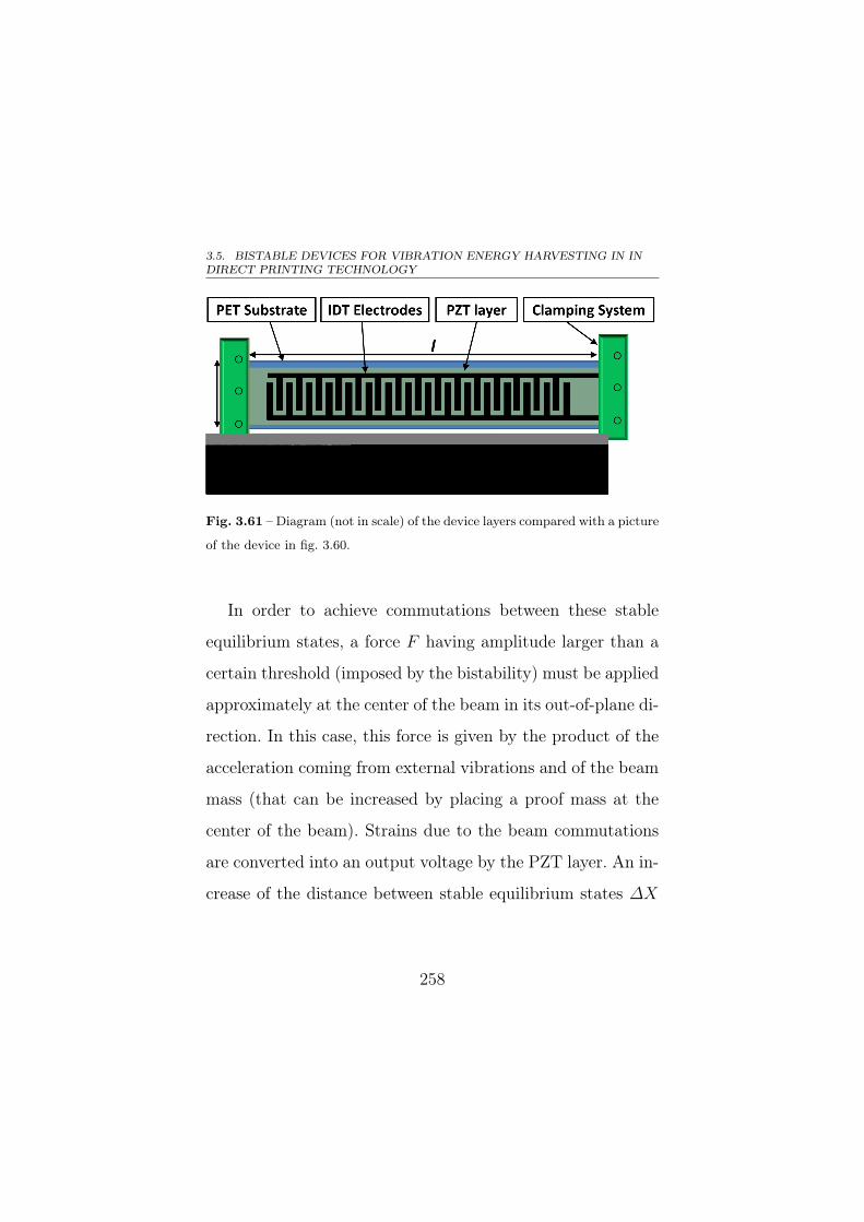
3.5. BISTABLE DEVICES FOR VIBRATION ENERGY HARVESTING IN INDIRECT PRINTING TECHNOLOGY
Fig. 3.61 – Diagram (not in scale) of the device layers compared with a picture
of the device in fig. 3.60.
In order to achieve commutations between these stable
equilibrium states, a force F having amplitude larger than a
certain threshold (imposed by the bistability) must be applied
approximately at the center of the beam in its out-of-plane di-
rection. In this case, this force is given by the product of the
acceleration coming from external vibrations and of the beam
mass (that can be increased by placing a proof mass at the
center of the beam). Strains due to the beam commutations
are converted into an output voltage by the PZT layer. An in-
crease of the distance between stable equilibrium states ∆X
258
CHAPTER 3. BISTABLE DEVICES FOR VIBRATION ENERGYHARVESTING
leads to a growth of both the output voltage V and the force
amplitude F required for commutations.
A proof mass madd can be added at centre of the beam
to reduce the level of the external acceleration aext descend-
ing from mechanical vibrations required to make the device
switching between its stable equilibrium states.
3.5.2 Design flow
The beam length l, width w, the applied displacement pre-
compression ∆Y and the eventual added proof mass madd are
the parameters to be designed before device realization. Pro-
cess parameters, such as layers thickness, are considered un-
changeable design constraints. The specification of this design
is the minimization of the minimum external static accelera-
tion astatic required to achieve device commutations by having
a minimum added proof mass aext.
The value of applied displacement precompression ∆Y is
bounded below by the critical compressive displacement ∆cr
determined by the values of beam length l and width w
through the (3.40). The energy specification of the system
is indicated by the system critical force Fc which is strictly
259
3.5. BISTABLE DEVICES FOR VIBRATION ENERGY HARVESTING IN INDIRECT PRINTING TECHNOLOGY
related to the distance ∆X between stable equilibrium states
for each pair of values of beam length l and width w and ap-
plied displacement precompression ∆Y . Critical force Fc and
distance ∆X can be determined through both FEM analyses
and mechanical characterization of the device prototypes.
By fixing the minimum required static acceleration aext
from the vibrational source taken into account, critical force
Fc is computed through the Newton’s Second Law [212] by
defining the eventual proof mass madd to be added to beam
mass. External static acceleration aext and eventual added
proof mass madd define the distance ∆X between stable equi-
librium states which, then, determines the value of the dis-
placement precompression ∆Y for each pair of beam length l
and width w (selected to optimize system dimension). Design
flow is summarized in fig. 3.62.
In this specific case study, the proposed design flow has
been applied to design a device capable of harvesting energy
from accelerations coming from a running/walking person.
An example of the typical waveforms and magnitude levels
of these accelerations is reported in figs. 3.2–3.3.
260
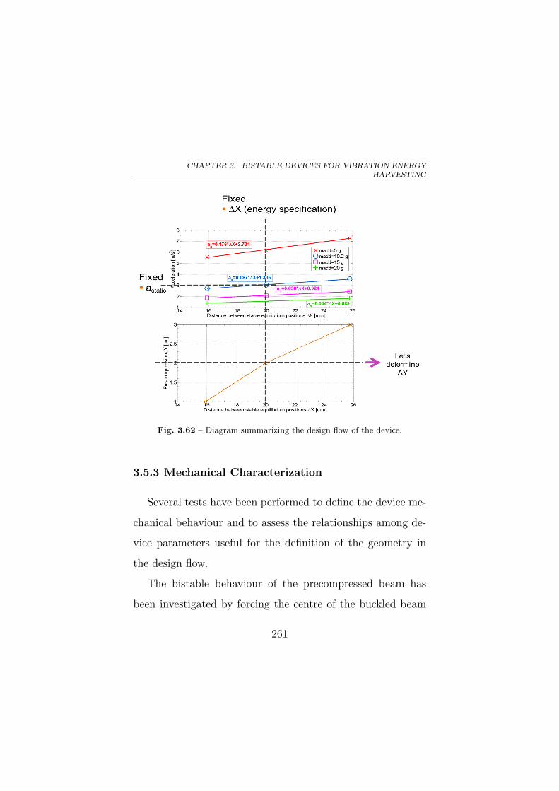
CHAPTER 3. BISTABLE DEVICES FOR VIBRATION ENERGYHARVESTING
Fig. 3.62 – Diagram summarizing the design flow of the device.
3.5.3 Mechanical Characterization
Several tests have been performed to define the device me-
chanical behaviour and to assess the relationships among de-
vice parameters useful for the definition of the geometry in
the design flow.
The bistable behaviour of the precompressed beam has
been investigated by forcing the centre of the buckled beam
261
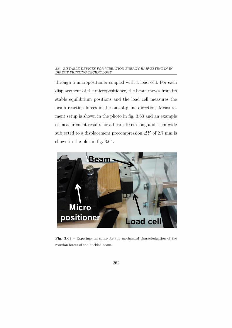
3.5. BISTABLE DEVICES FOR VIBRATION ENERGY HARVESTING IN INDIRECT PRINTING TECHNOLOGY
through a micropositioner coupled with a load cell. For each
displacement of the micropositioner, the beam moves from its
stable equilibrium positions and the load cell measures the
beam reaction forces in the out-of-plane direction. Measure-
ment setup is shown in the photo in fig. 3.63 and an example
of measurement results for a beam 10 cm long and 1 cm wide
subjected to a displacement precompression ∆Y of 2.7 mm is
shown in the plot in fig. 3.64.
Fig. 3.63 – Experimental setup for the mechanical characterization of the
reaction forces of the buckled beam.
262
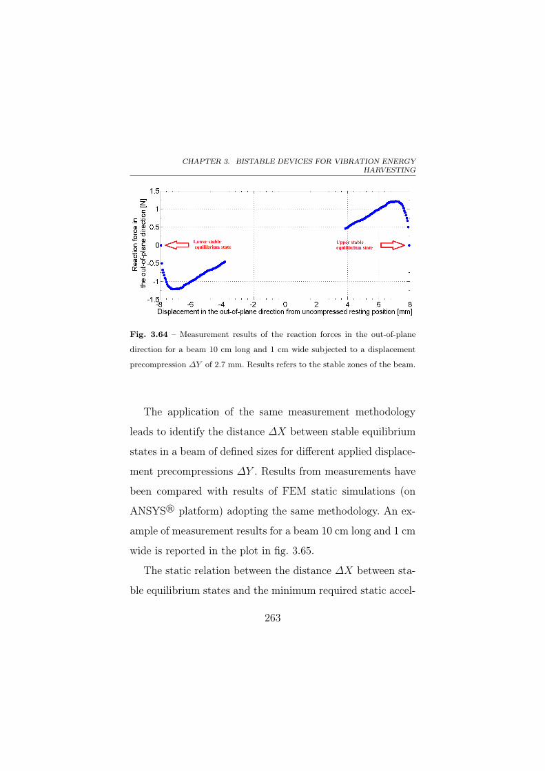
CHAPTER 3. BISTABLE DEVICES FOR VIBRATION ENERGYHARVESTING
Fig. 3.64 – Measurement results of the reaction forces in the out-of-plane
direction for a beam 10 cm long and 1 cm wide subjected to a displacement
precompression ∆Y of 2.7 mm. Results refers to the stable zones of the beam.
The application of the same measurement methodology
leads to identify the distance ∆X between stable equilibrium
states in a beam of defined sizes for different applied displace-
ment precompressions ∆Y . Results from measurements have
been compared with results of FEM static simulations (on
ANSYS® platform) adopting the same methodology. An ex-
ample of measurement results for a beam 10 cm long and 1 cm
wide is reported in the plot in fig. 3.65.
The static relation between the distance ∆X between sta-
ble equilibrium states and the minimum required static accel-
263
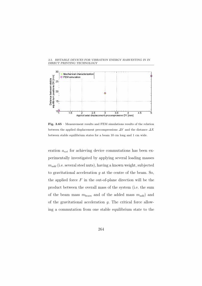
3.5. BISTABLE DEVICES FOR VIBRATION ENERGY HARVESTING IN INDIRECT PRINTING TECHNOLOGY
Fig. 3.65 – Measurement results and FEM simulations results of the relation
between the applied displacement precompressions ∆Y and the distance ∆X
between stable equilibrium states for a beam 10 cm long and 1 cm wide.
eration aext for achieving device commutations has been ex-
perimentally investigated by applying several loading masses
madd (i.e. several steel nuts), having a known weight, subjected
to gravitational acceleration g at the centre of the beam. So,
the applied force F in the out-of-plane direction will be the
product between the overall mass of the system (i.e. the sum
of the beam mass mbeam and of the added mass madd) and
of the gravitational acceleration g. The critical force allow-
ing a commutation from one stable equilibrium state to the
264
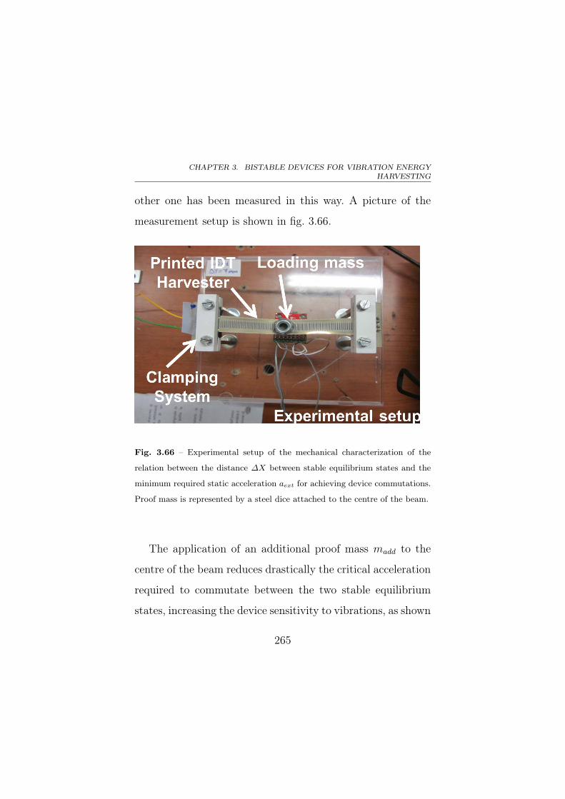
CHAPTER 3. BISTABLE DEVICES FOR VIBRATION ENERGYHARVESTING
other one has been measured in this way. A picture of the
measurement setup is shown in fig. 3.66.
Fig. 3.66 – Experimental setup of the mechanical characterization of the
relation between the distance ∆X between stable equilibrium states and the
minimum required static acceleration aext for achieving device commutations.
Proof mass is represented by a steel dice attached to the centre of the beam.
The application of an additional proof mass madd to the
centre of the beam reduces drastically the critical acceleration
required to commutate between the two stable equilibrium
states, increasing the device sensitivity to vibrations, as shown
265
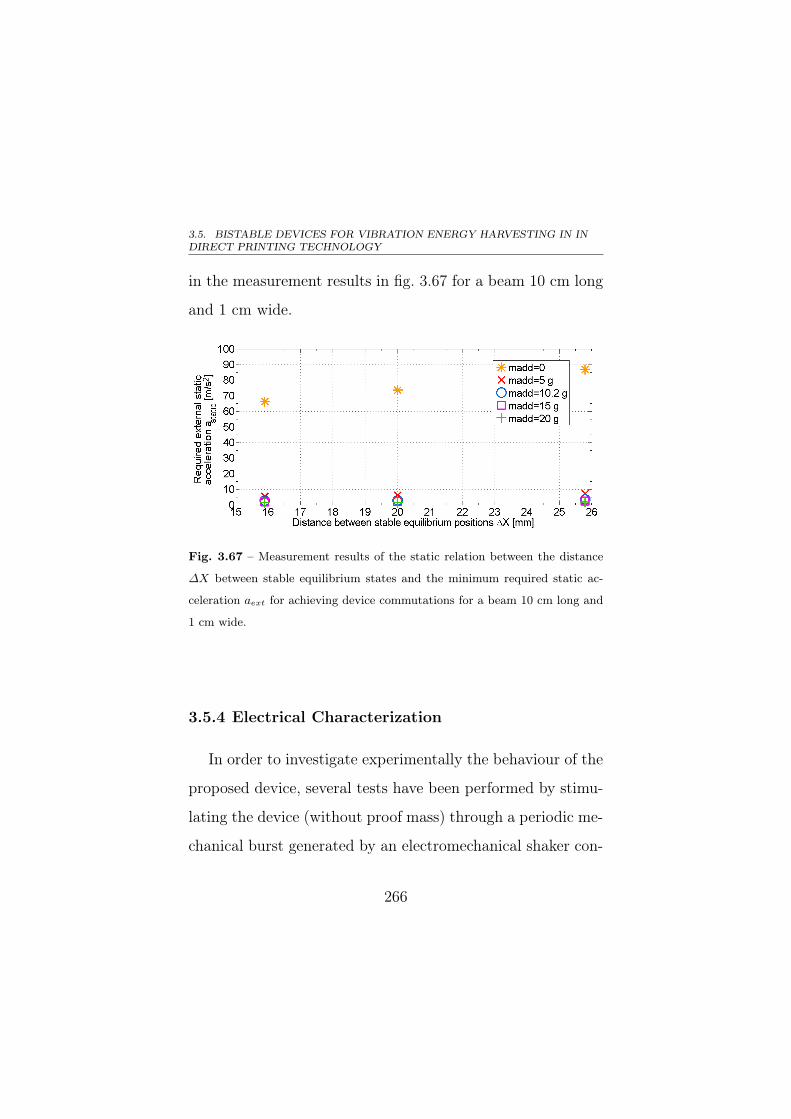
3.5. BISTABLE DEVICES FOR VIBRATION ENERGY HARVESTING IN INDIRECT PRINTING TECHNOLOGY
in the measurement results in fig. 3.67 for a beam 10 cm long
and 1 cm wide.
Fig. 3.67 – Measurement results of the static relation between the distance
∆X between stable equilibrium states and the minimum required static ac-
celeration aext for achieving device commutations for a beam 10 cm long and
1 cm wide.
3.5.4 Electrical Characterization
In order to investigate experimentally the behaviour of the
proposed device, several tests have been performed by stimu-
lating the device (without proof mass) through a periodic me-
chanical burst generated by an electromechanical shaker con-
266
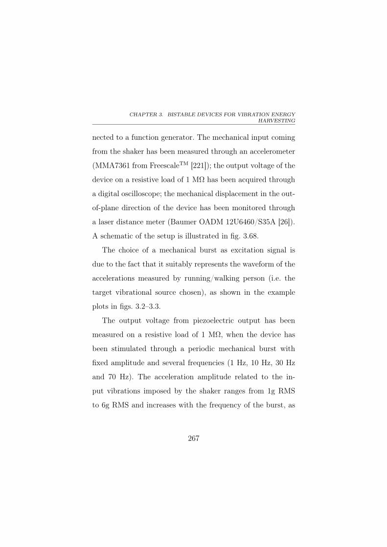
CHAPTER 3. BISTABLE DEVICES FOR VIBRATION ENERGYHARVESTING
nected to a function generator. The mechanical input coming
from the shaker has been measured through an accelerometer
(MMA7361 from FreescaleTM [221]); the output voltage of the
device on a resistive load of 1 MΩ has been acquired through
a digital oscilloscope; the mechanical displacement in the out-
of-plane direction of the device has been monitored through
a laser distance meter (Baumer OADM 12U6460/S35A [26]).
A schematic of the setup is illustrated in fig. 3.68.
The choice of a mechanical burst as excitation signal is
due to the fact that it suitably represents the waveform of the
accelerations measured by running/walking person (i.e. the
target vibrational source chosen), as shown in the example
plots in figs. 3.2–3.3.
The output voltage from piezoelectric output has been
measured on a resistive load of 1 MΩ, when the device has
been stimulated through a periodic mechanical burst with
fixed amplitude and several frequencies (1 Hz, 10 Hz, 30 Hz
and 70 Hz). The acceleration amplitude related to the in-
put vibrations imposed by the shaker ranges from 1g RMS
to 6g RMS and increases with the frequency of the burst, as
267
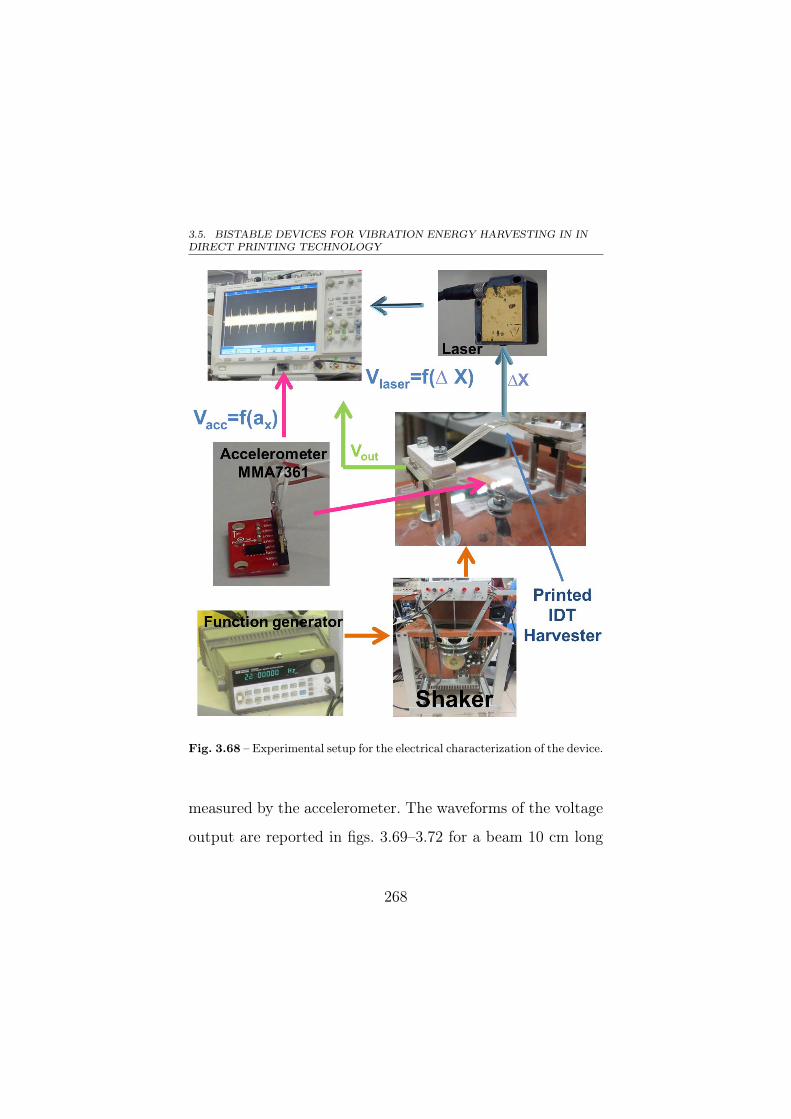
3.5. BISTABLE DEVICES FOR VIBRATION ENERGY HARVESTING IN INDIRECT PRINTING TECHNOLOGY
Fig. 3.68 – Experimental setup for the electrical characterization of the device.
measured by the accelerometer. The waveforms of the voltage
output are reported in figs. 3.69–3.72 for a beam 10 cm long
268
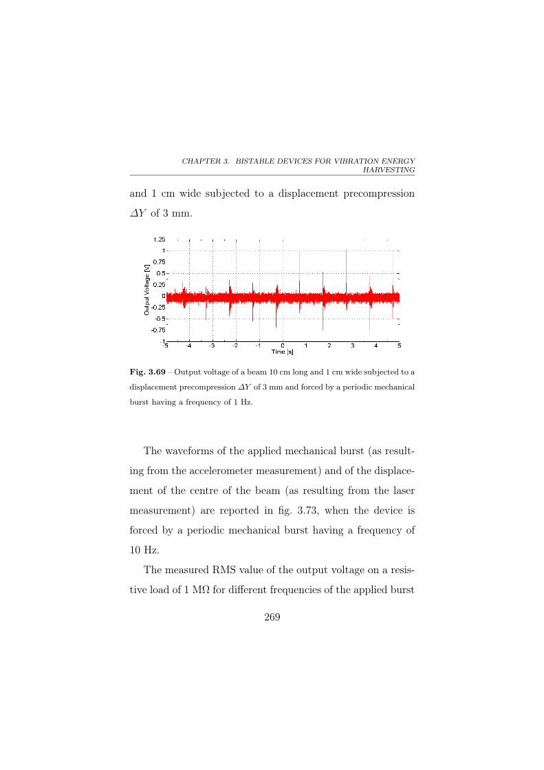
CHAPTER 3. BISTABLE DEVICES FOR VIBRATION ENERGYHARVESTING
and 1 cm wide subjected to a displacement precompression
∆Y of 3 mm.
Fig. 3.69 – Output voltage of a beam 10 cm long and 1 cm wide subjected to a
displacement precompression ∆Y of 3 mm and forced by a periodic mechanical
burst having a frequency of 1 Hz.
The waveforms of the applied mechanical burst (as result-
ing from the accelerometer measurement) and of the displace-
ment of the centre of the beam (as resulting from the laser
measurement) are reported in fig. 3.73, when the device is
forced by a periodic mechanical burst having a frequency of
10 Hz.
The measured RMS value of the output voltage on a resis-
tive load of 1 MΩ for different frequencies of the applied burst
269
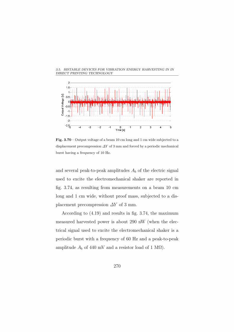
3.5. BISTABLE DEVICES FOR VIBRATION ENERGY HARVESTING IN INDIRECT PRINTING TECHNOLOGY
Fig. 3.70 – Output voltage of a beam 10 cm long and 1 cm wide subjected to a
displacement precompression ∆Y of 3 mm and forced by a periodic mechanical
burst having a frequency of 10 Hz.
and several peak-to-peak amplitudes Ab of the electric signal
used to excite the electromechanical shaker are reported in
fig. 3.74, as resulting from measurements on a beam 10 cm
long and 1 cm wide, without proof mass, subjected to a dis-
placement precompression ∆Y of 3 mm.
According to (4.19) and results in fig. 3.74, the maximum
measured harvested power is about 290 nW (when the elec-
trical signal used to excite the electromechanical shaker is a
periodic burst with a frequency of 60 Hz and a peak-to-peak
amplitude Ab of 440 mV and a resistor load of 1 MΩ).
270
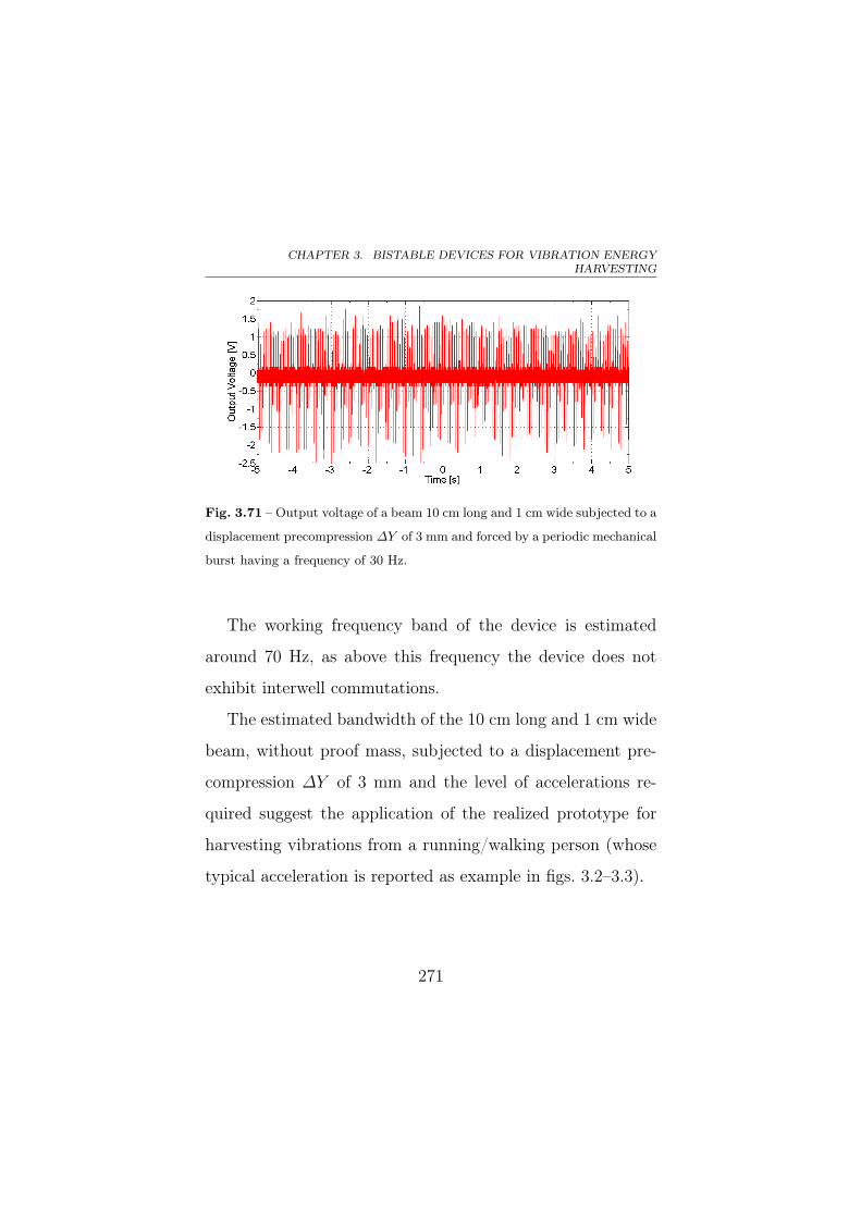
CHAPTER 3. BISTABLE DEVICES FOR VIBRATION ENERGYHARVESTING
Fig. 3.71 – Output voltage of a beam 10 cm long and 1 cm wide subjected to a
displacement precompression ∆Y of 3 mm and forced by a periodic mechanical
burst having a frequency of 30 Hz.
The working frequency band of the device is estimated
around 70 Hz, as above this frequency the device does not
exhibit interwell commutations.
The estimated bandwidth of the 10 cm long and 1 cm wide
beam, without proof mass, subjected to a displacement pre-
compression ∆Y of 3 mm and the level of accelerations re-
quired suggest the application of the realized prototype for
harvesting vibrations from a running/walking person (whose
typical acceleration is reported as example in figs. 3.2–3.3).
271
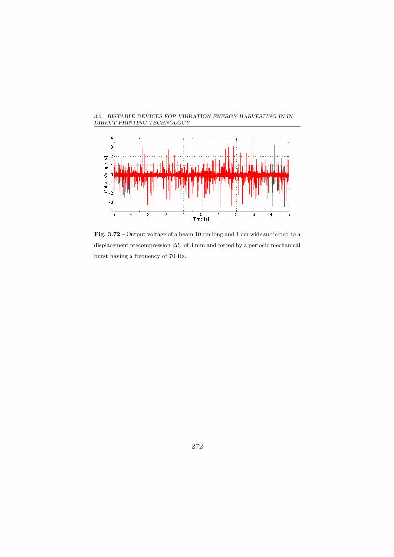
3.5. BISTABLE DEVICES FOR VIBRATION ENERGY HARVESTING IN INDIRECT PRINTING TECHNOLOGY
Fig. 3.72 – Output voltage of a beam 10 cm long and 1 cm wide subjected to a
displacement precompression ∆Y of 3 mm and forced by a periodic mechanical
burst having a frequency of 70 Hz.
272
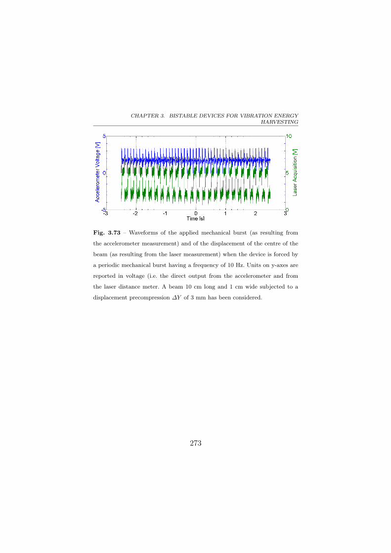
CHAPTER 3. BISTABLE DEVICES FOR VIBRATION ENERGYHARVESTING
Fig. 3.73 – Waveforms of the applied mechanical burst (as resulting from
the accelerometer measurement) and of the displacement of the centre of the
beam (as resulting from the laser measurement) when the device is forced by
a periodic mechanical burst having a frequency of 10 Hz. Units on y-axes are
reported in voltage (i.e. the direct output from the accelerometer and from
the laser distance meter. A beam 10 cm long and 1 cm wide subjected to a
displacement precompression ∆Y of 3 mm has been considered.
273
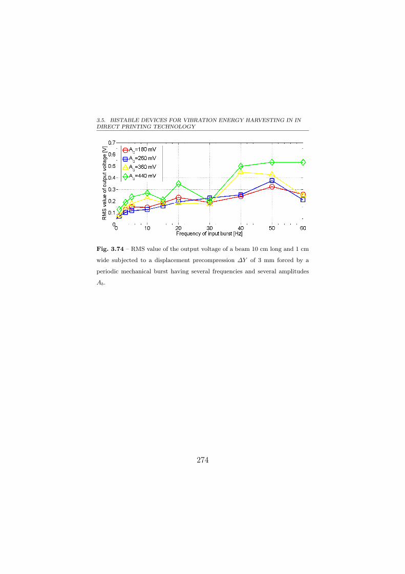
3.5. BISTABLE DEVICES FOR VIBRATION ENERGY HARVESTING IN INDIRECT PRINTING TECHNOLOGY
Fig. 3.74 – RMS value of the output voltage of a beam 10 cm long and 1 cm
wide subjected to a displacement precompression ∆Y of 3 mm forced by a
periodic mechanical burst having several frequencies and several amplitudes
Ab.
274

4
Bistable devices for AC current
sensors
I happen to have discovered a direct relation between magnetism and light,
also electricity and light, and the field it opens is so large and I think rich.
Michael Faraday
In this chapter, a nonlinear methodology to improve the
sensitivity in measuring AC electrical currents in certain op-
erating conditions and to ensure autonomous sensor operation
will be presented along with device simulations and exper-
imental results to assess the feasibility of the proposed ap-
proach.
4.1. STATE OF ART FOR AC CURRENT SENSORS
4.1 State of art for AC current sensors
The need for ubiquitous and autonomous sensors for sens-
ing electrical quantities represents one of the most important
motivating reasons for research efforts spent in the scientific
field. In fact, increasing global requests for energy efficiency,
development of smart-grids and advances in compact sensor
network technologies push researchers to study novel types
of sensors in order to efficiently monitor electricity usage in
power lines both in residential, industrial and commercial en-
vironments and in distribution and transmission power sys-
tems [153].
Among electrical quantities a special attention is deserved
to AC electrical currents in order to monitor power consump-
tion in electric systems [250].
An overview on techniques for current sensing is presented
in subsection 4.1.1 and, due to the topic in this work, more
details on MEMS AC current sensors will be discussed in sub-
section 4.1.2.
276
CHAPTER 4. BISTABLE DEVICES FOR AC CURRENT SENSORS
4.1.1 Techniques for current sensing
Shunt resistor, transformers, and magnetic field sensors are
traditional technologies adopted to measure a current flowing
in a wire [249].
Shunt resistors techniques are used to directly measure the
amount of current through a resistive element placed in series
with the load. The principle is based on Ohm’s law where the
voltage drop across the device is proportional to the flowing
current. This technology can provide an accurate measure-
ment for low currents, but in the case of large currents it is
very impractical because the shunts become bulky and heavy
and the voltage drop causes large heat dissipation. Further-
more, some mounting issues are noticed, their measurement is
affected by insertion loss and other circuitry, such as instru-
mentation amplifiers, are needed to generate distinguishable
signals for measurement [130].
Transformer techniques are passive methodologies adopted
to indirectly measure the current through the secondary wind-
ing of a current transformer. Current transformers are rela-
tively simple to implement and are passive devices that do not
277
4.1. STATE OF ART FOR AC CURRENT SENSORS
require driving circuitry to operate. These transformers have
a primary coil with a few turns and a secondary coil which
should ideally be short circuits, see fig. 4.1(a). The primary
AC current will generate a magnetic field which is coupled
into secondary coil by Faraday’s law. The magnitude of the
secondary current is proportional to the number of turns in
the coil, which is typically higher than 1000. Secondary cur-
rent is then sensed through a sensing resistor to convert the
output to voltage. Current transformers amplitude and phase
errors depend on the core material and size, coil geometry, am-
plitude and frequency of the measured current, and also on
the value of the load. Advantages of current transformers are:
contact-less current measurement, detecting of high currents,
low power consumption, and low temperature shift [259].
Several techniques of current sensing have been developed
by exploiting magnetic field sensors, whose technology and
applications have been in a great interest and in a constant
growth in scientific research in last decades [140, 141]. The
main advantage of this current sensing technique is sensing
the magnetic field produced by the current under test in a
278
CHAPTER 4. BISTABLE DEVICES FOR AC CURRENT SENSORS
contactless measurement, due to the safety needed in the case
of high current measurement.
Hall sensors are among the most commonly used types of
magnetic field sensors. According to the Hall Effect princi-
ple, the magnetic force on a moving electron in a conductor
will produce a slight displacement between the electrons and
the positive ions of the stationary lattice structures. As a re-
sult of this, a voltage will be generated perpendicular to both
the current and the field. This principle is known as Hall Ef-
fect [186]. In the case of current sensors based on Hall Effect,
when a magnetic field is perpendicular to a current in a thin
metal sheet, a Lorentz force is exerted on the current. This
force disturbs the current distribution, resulting in a poten-
tial difference across the output, see fig. 4.1(b). This voltage
is called “Hall voltage” and is directly proportional to the cur-
rent and the magnetic field, albeit of being of very small in
order (micro-Tesla) [69]. The most sensitive Hall sensors are
made of Indium antimonide (InSb) and III-V semiconductors,
which require dedicated fabrication processes [219].
279
4.1. STATE OF ART FOR AC CURRENT SENSORS
Rogowski coil, also known as “di/dt coil”, is used to mea-
sure AC current, transient current and changes in DC current.
It is based on search coil technique for sensing magnetic field.
It is made of coil with or without core [121, 247]. The oper-
ation principle of these sensors is based on Faraday’s Law of
Induction [212]. If the magnetic flux inside the coil changes, a
voltage proportional to the rate of change of the flux is gen-
erated between the coil leads. The sensitivity of the search
coil depends on the magnetic permeability of the core mate-
rial (ferromagnetic core increases the sensitivity), the area of
the coil, the number of turns and the rate of change of the
magnetic flux through the coil. The Rogowski coil is designed
to cancel the far field while the near field will remain. This is
to avoid the possibility of interference occurring which is usu-
ally far field related. Rogowski devices are extremely linear
and have air cores which make construction simple. However,
in terms of signal processing, the output of the coil should
be integrated because it is sensitive to the rate of the cur-
rent, see general scheme in fig. 4.1(c). The advantage that
the Rogowski coil has in addition to current transformers is
280
CHAPTER 4. BISTABLE DEVICES FOR AC CURRENT SENSORS
that no DC or high current saturation is possible. This is
because the saturation of the air-core in a Rogowski coil is
extremely high compared with ferrite cores of normal current
transformers. The air core also has a linear phase response
and low cost [197].
Fluxgate sensors measure the magnitude and direction of
the DC or low AC magnetic field with high sensitivity in the
range between several tens of nano-Tesla and tens of milli-
Tesla [198]. As all ferromagnetic materials exhibit hysteresis,
a sinusoidal current applied to drive coil causes the core to
reach its saturation magnetization once every half cycle. The
sense coil then detects a nonlinearIy distorted signal, see gen-
eral scheme in fig. 4.1(d). The output signal includes even har-
monics of the drive signal, and most importantly, the second
harmonic. The voltage associated with harmonics is propor-
tional to the external magnetic field [68].
Superconducting Quantum Interference Devices (SQUID)
are one of the most sensitive magnetic sensors available. The
sensitivity of these sensors is on the order of femto-Teslas [71].
Besides their use in the laboratory, they have a rich applica-
281

4.1. STATE OF ART FOR AC CURRENT SENSORS
Fig. 4.1 – General schemes of current sensing techniques: (a) current trans-
former, (b) Hall Effect, (c) Rogowski coil and (d) fluxgate magnetometer.
tion potential in areas such as geophysics, bio-magnetism and
non-destructive testing of materials. The basic phenomena
governing the operation of SQUID devices are flux quantiza-
tion in superconducting loops and the Josephson Effect [251].
One of the main applications besides current measurement is
in medical imaging purposes, whereby measuring the neuro-
magnetic field of the humans [72].
282
CHAPTER 4. BISTABLE DEVICES FOR AC CURRENT SENSORS
Other techniques for current measurement are based on
nuclear precession [149], fiber optic with magnetostrictive ma-
terials [209], magnetoresistors [119], magnetodiodes [185] and
magnetotransistors [233].
Because of the scope of this work, a special attention is
deserved to micromechanical AC current sensors, which will
be illustrated with more details in subsection 4.1.2.
4.1.2 MEMS AC current sensors
Most MEMS sensors are based on mechanical microstruc-
tures technology, which uses a broad range of design mate-
rials and mechanical structures. The benefit of MEMS tech-
nology is in the development of miniaturized devices with a
lower cost, lower power consumption, higher performance and
greater integration for batch production [131].
The deposition of functional magnetic materials on mi-
crostructures, such as cantilever beams, enables the possibility
to exploit MEMS devices in magnetic field sensing applica-
tions and, thus, to detect and measure time-variable electric
currents, that are sources of magnetic fields. Among time-
variable currents, AC electrical currents (thus generating an
283
4.1. STATE OF ART FOR AC CURRENT SENSORS
oscillating alternate magnetic field) play a central role in elec-
tric systems because the current delivered by power systems
is sinusoidal (at a frequency of 50 Hz or 60 Hz, depending on
the countries) and switching systems are widely used in power
converters [163].
Using this approach, several microcantilevers capable of
detecting magnetic fields [61] have been developed. Some of
them have also an accurate angle detection capability [123].
Traditionally, MEMS sensors for AC electrical currents are
based on the interaction between a magnetic field generated
by the electrical current to be measured and a magnetic field
produced by the sensor [137]. The magnetic field coming from
the sensor can be generated either by using coils where a sec-
ondary electrical current is forced by the sensor [23] or by
adopting magnetic materials like permanent magnets [197].
To this aim, other materials capable of interacting with the
external magnetic field, such as cobalt, have been used in coat-
ings of cantilever beams too [96]. Sensors exploiting Lorentz
forces [122] and eddy currents [206] have been also proposed.
284
CHAPTER 4. BISTABLE DEVICES FOR AC CURRENT SENSORS
This strategy has the advantage of contactless operation,
even if the distance between the sensor and the source should
be very small for the feasibility of the principles.
The approach based on permanent magnets is preferred be-
cause permanent magnets do not require power and condition-
ing circuitry to generate a magnetic filed. However solutions
using actuation currents or magnetic coatings are desirable in
microsystems applications where the microfabrication of per-
manent magnets, especially having a given magnetization, can
be seriously challenging.
The magnetic force generated by the aforesaid magnetic in-
teraction is commonly used to actuate a mechanical vibrating
structure. Typically, this structure consists of a linear reso-
nant mechanism tuned with the frequency of the AC electri-
cal current to be measured (e.g. a cantilever beam equipped
with a permanent magnet or coils on its free end) and that
gives a linear response [111], in terms of relation between the
magnitude of AC current and the amplitude of mechanical
oscillation of the microstructure. Resonating microstructures
have the advantage of providing a large output signal. For
285
4.1. STATE OF ART FOR AC CURRENT SENSORS
this reason, many micromechanical sensors have exploited this
advantage to improve their sensitivity or dynamic range, al-
though they could suffer from certain operating conditions,
such as noisy environments, or low levels of target currents
(see subsection 1.3.1) [122].
Displacements and strains of the oscillating structure due
to magnetic interaction forces are electrically sensed through
piezoresistors [30] or variable capacitors [78]: these approaches
require external powering. Sometimes capacitive sensing has
been used to correct nonlinearities of resonant sensors through
a feedback logic [122]. Optical readout [124] is also adopted
at the price of higher complexities (e.g., use of laser and/or
optical fibres). Another readout strategy is based on piezo-
electric strategies employing self-generating materials, such
as Lead Titanate Zirconate (PZT) and Aluminium Nitride
(AlN), which provide autonomous solutions without external
powering [178]; an example of piezoelectric resonant AC cur-
rent sensor proposed in literature is illustrated in fig. 4.2
286
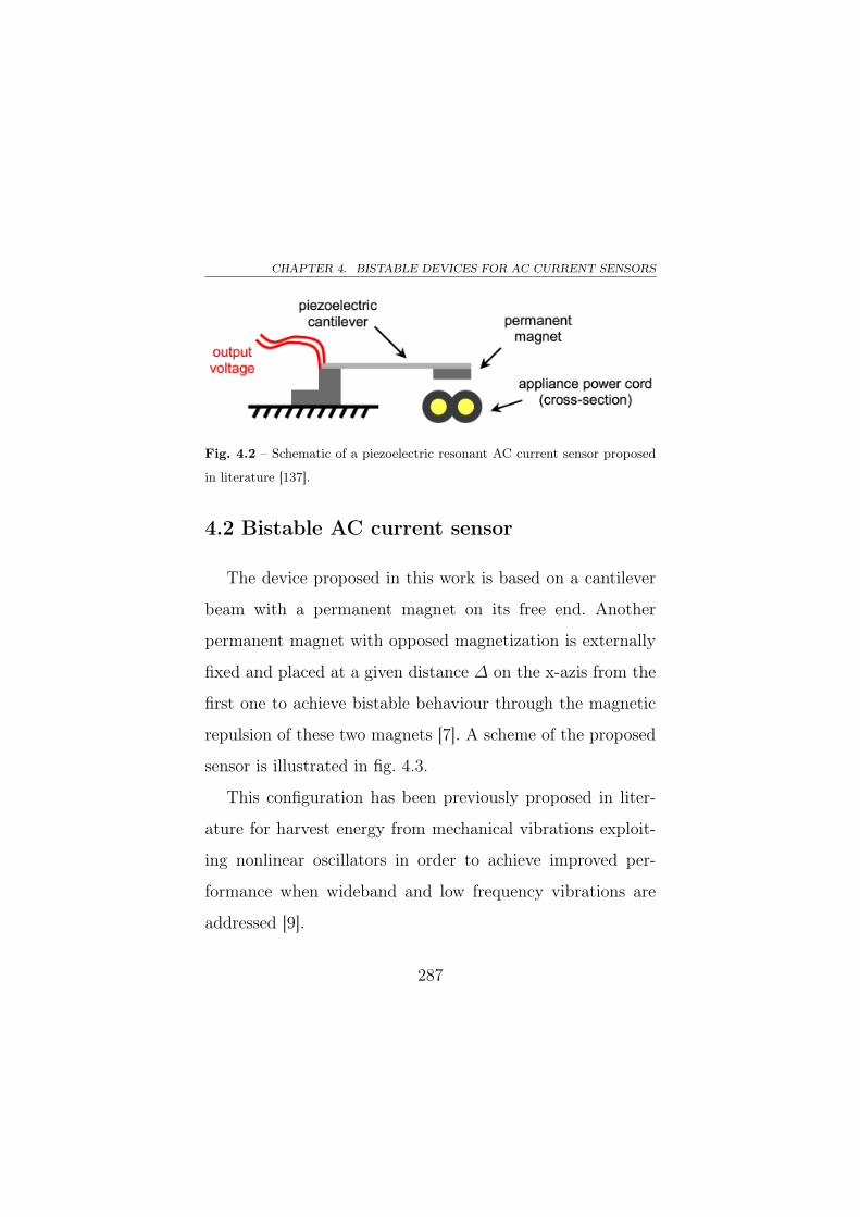
CHAPTER 4. BISTABLE DEVICES FOR AC CURRENT SENSORS
Fig. 4.2 – Schematic of a piezoelectric resonant AC current sensor proposed
in literature [137].
4.2 Bistable AC current sensor
The device proposed in this work is based on a cantilever
beam with a permanent magnet on its free end. Another
permanent magnet with opposed magnetization is externally
fixed and placed at a given distance ∆ on the x-azis from the
first one to achieve bistable behaviour through the magnetic
repulsion of these two magnets [7]. A scheme of the proposed
sensor is illustrated in fig. 4.3.
This configuration has been previously proposed in liter-
ature for harvest energy from mechanical vibrations exploit-
ing nonlinear oscillators in order to achieve improved per-
formance when wideband and low frequency vibrations are
addressed [9].
287
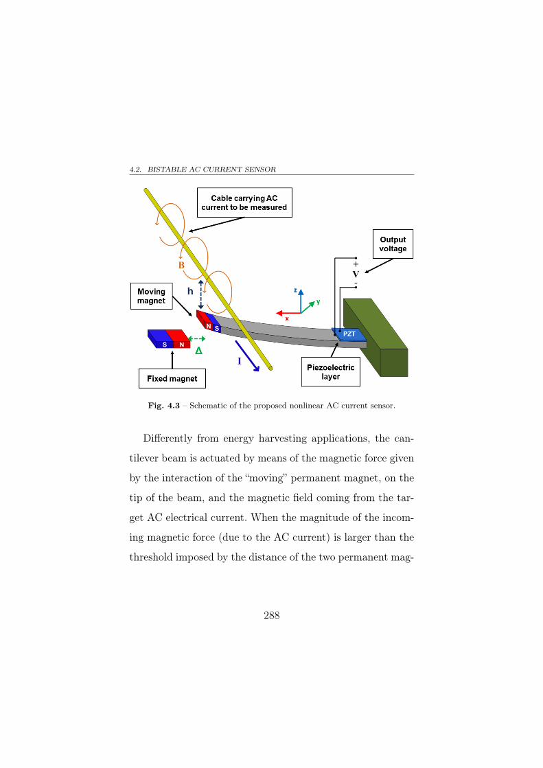
4.2. BISTABLE AC CURRENT SENSOR
Fig. 4.3 – Schematic of the proposed nonlinear AC current sensor.
Differently from energy harvesting applications, the can-
tilever beam is actuated by means of the magnetic force given
by the interaction of the “moving” permanent magnet, on the
tip of the beam, and the magnetic field coming from the tar-
get AC electrical current. When the magnitude of the incom-
ing magnetic force (due to the AC current) is larger than the
threshold imposed by the distance of the two permanent mag-
288
CHAPTER 4. BISTABLE DEVICES FOR AC CURRENT SENSORS
nets, the system snaps from one stable equilibrium state to
the other one, triggering some commutations.
A piezoelectric layer provides a mechanical-to-electrical
transduction of the mechanical displacements and velocities
of the structure and ensures the autonomous operation of the
device.
The number of commutations between the two stable states,
in a defined period of time and with a fixed bistable thresh-
old, grows by increasing the amount of the incoming electrical
current until a saturation level is reached: this directly pro-
vides a digital measurement of the current. In fact, systems
commutations can be easily counted through digital counters
by considering the output from the piezoelectric layer.
Another advantage is given by the increased sensitivity of
the device: in fact, whichever will be the amount of the electri-
cal current above the fixed bistable thresholds and in the op-
erative range of the sensor (easily tuned by adjusting the dis-
tance ∆ between permanent magnets), the amplitude and the
duration of each commutation and, consequently, the ampli-
tude of the output piezoelectric signal will not roughly change,
289
4.2. BISTABLE AC CURRENT SENSOR
differently from strategies based on resonant cantilevers that
provide a linear output. This makes the system more robust
to external noise (e.g., electrical noise in power lines and me-
chanical noise from mechanical vibrations in the operative
environment of the device), especially when weak electric cur-
rents have to be measured [92].
Considering the bistable transduction mechanism imple-
mented in this sensor, this device takes advantage of all the
benefits descending from stochastic resonance and the inter-
play between nonlinearity and noise in “Noise Activated Non-
linear Dynamic Sensors” [88], as discussed in subsection 1.3.1.
In fact, electrical noise in power lines, mechanical noise from
mechanical vibrations in the operative environment of the de-
vice and the deterministic sinusoidal signal of the AC target
current can be related to the theory of stochastic resonance
(see eq. (1.8) in subsection 1.3.1) and exploited to enhance
sensing performance of the device, in terms of sensitivity and
responsivity, in certain operating conditions that can be un-
favorable to linear resonant sensors (e.g., high levels of noise
and weak target signals).
290
CHAPTER 4. BISTABLE DEVICES FOR AC CURRENT SENSORS
The output voltage from the piezoelectric layer can be used
both as signal to carry information from the sensor operation
of the device and as energy harvested from the beam commu-
tations (that can be used to power the sensor and/or other
electronic circuits ensuring sensor operation, e.g., in a wire-
less sensor node). In fact, beam commutations can be caused
by both the magnetic field from the target current and also
by mechanical vibrations in the operating environment of the
device, thus, including in the same device a sensor and an en-
ergy harvester [7]. In this case, the benefits of the interplay be-
tween noise and nonlinearity in periodically-forced nonlinear
oscillators is exploited both in enhancing quality and quantity
of extracted information and in scavenging more energy [40,
235].
The adoption of a nonlinear oscillating structure, thus
avoiding the use of resonant structures, prevents the issues
of matching the frequency of the resonant structures with the
one of the electrical current to be measured. In fact, the re-
alization of linear resonant structures with very low resonant
frequencies (such as 50 Hz or 60 Hz, i.e. the most used fre-
291
4.3. BISTABLE AC CURRENT SENSOR MODELING
quency of the delivered currents in the power lines in many
countries) is very difficult at microscale [17].
The development of this device at microscale (e.g. its in-
tegration in a chip) will allow its insertion into the shields
of cables (i.e. between the cables and their shields). The re-
duction of the system dimensions (the cantilever beam and
the permanent magnets) will also decrease the amount of the
magnetic force required for the commutations of the beam and
will allow its placement at a distance of or below a millimeter
size.
The model of the proposed device will be discussed in sec-
tion 4.3.
4.3 Bistable AC current sensor modeling
The system is composed of a vibrating structure and two
permanent magnets, one fixed and one moving. With refer-
ence to the scheme in fig. 4.3, the vibrating structure of the
system consists in a cantilever beam having a length l (on
x-axis), a width w (on y-axis) and a thickness t (on z-axis). A
piezoelectric layer of thickness tPZT (on z-axis), width wPZT
292
CHAPTER 4. BISTABLE DEVICES FOR AC CURRENT SENSORS
(on y-axis) and length lPZT (on x-axis) is placed on the me-
chanical layer of the cantilever beam in order to implement a
self-generating piezoelectric readout for the sensor. A perma-
nent magnet (i.e. the moving permanent magnet) of volume
Vm, mass density ρm and magnetic remanence Br is attached
to the top of the free end of the beam, while another magnet,
the fixed permanent magnet, having the same properties as
the moving permanent magnet, but opposed magnetization, is
placed on a fixed base at a distance ∆ from the moving mag-
net. The length of the cantilever beam is along x-axis and
the main displacement of its free end is along z-axis. The AC
electrical current to be measured I(t) flows in a wire placed
along the z-axis and at a minimum distance h (measured along
x-axis) from the magnet placed at the tip of the beam. Let
z be the relative displacement of the cantilever beam from
its fabrication position (z = 0), the 1 DOF lumped parame-
ter model is defined by (4.1) (derived from (3.7), after slight
modifications).
293
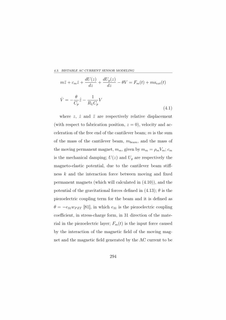
4.3. BISTABLE AC CURRENT SENSOR MODELING
mz + cmz +dU(z)
dz+dUg(z)
dz− θV = Fm(t) +maext(t)
V = − θ
Cp˙z − 1
RLCpV
(4.1)
where z, z and z are respectively relative displacement
(with respect to fabrication position, z = 0), velocity and ac-
celeration of the free end of the cantilever beam; m is the sum
of the mass of the cantilever beam, mbeam, and the mass of
the moving permanent magnet,mm, given bymm = ρmVm; cm
is the mechanical damping; U(z) and Ug are respectively the
magneto-elastic potential, due to the cantilever beam stiff-
ness k and the interaction force between moving and fixed
permanent magnets (which will calculated in (4.10)), and the
potential of the gravitational forces defined in (4.13); θ is the
piezoelectric coupling term for the beam and it is defined as
θ = −e31wPZT [81], in which e31 is the piezoelectric coupling
coefficient, in stress-charge form, in 31 direction of the mate-
rial in the piezoelectric layer; Fm(t) is the input force caused
by the interaction of the magnetic field of the moving mag-
net and the magnetic field generated by the AC current to be
294
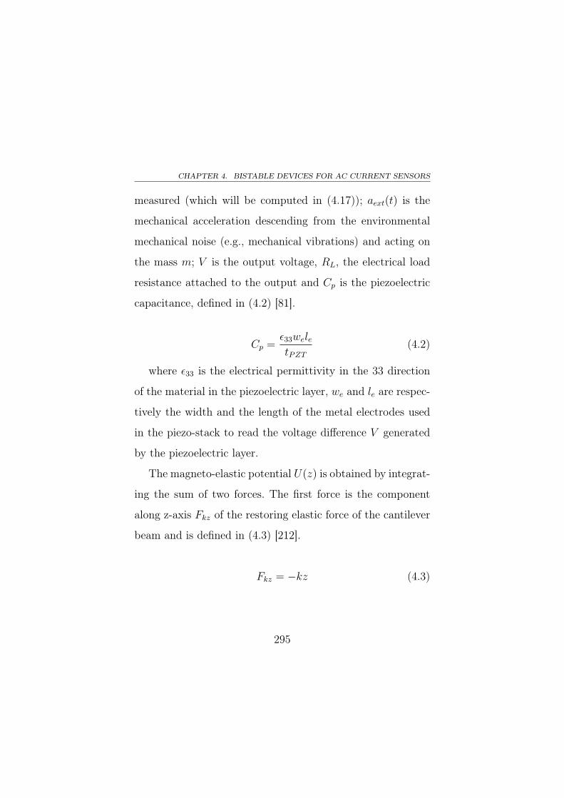
CHAPTER 4. BISTABLE DEVICES FOR AC CURRENT SENSORS
measured (which will be computed in (4.17)); aext(t) is the
mechanical acceleration descending from the environmental
mechanical noise (e.g., mechanical vibrations) and acting on
the mass m; V is the output voltage, RL, the electrical load
resistance attached to the output and Cp is the piezoelectric
capacitance, defined in (4.2) [81].
Cp =ε33weletPZT
(4.2)
where ε33 is the electrical permittivity in the 33 direction
of the material in the piezoelectric layer, we and le are respec-
tively the width and the length of the metal electrodes used
in the piezo-stack to read the voltage difference V generated
by the piezoelectric layer.
The magneto-elastic potential U(z) is obtained by integrat-
ing the sum of two forces. The first force is the component
along z-axis Fkz of the restoring elastic force of the cantilever
beam and is defined in (4.3) [212].
Fkz = −kz (4.3)
295
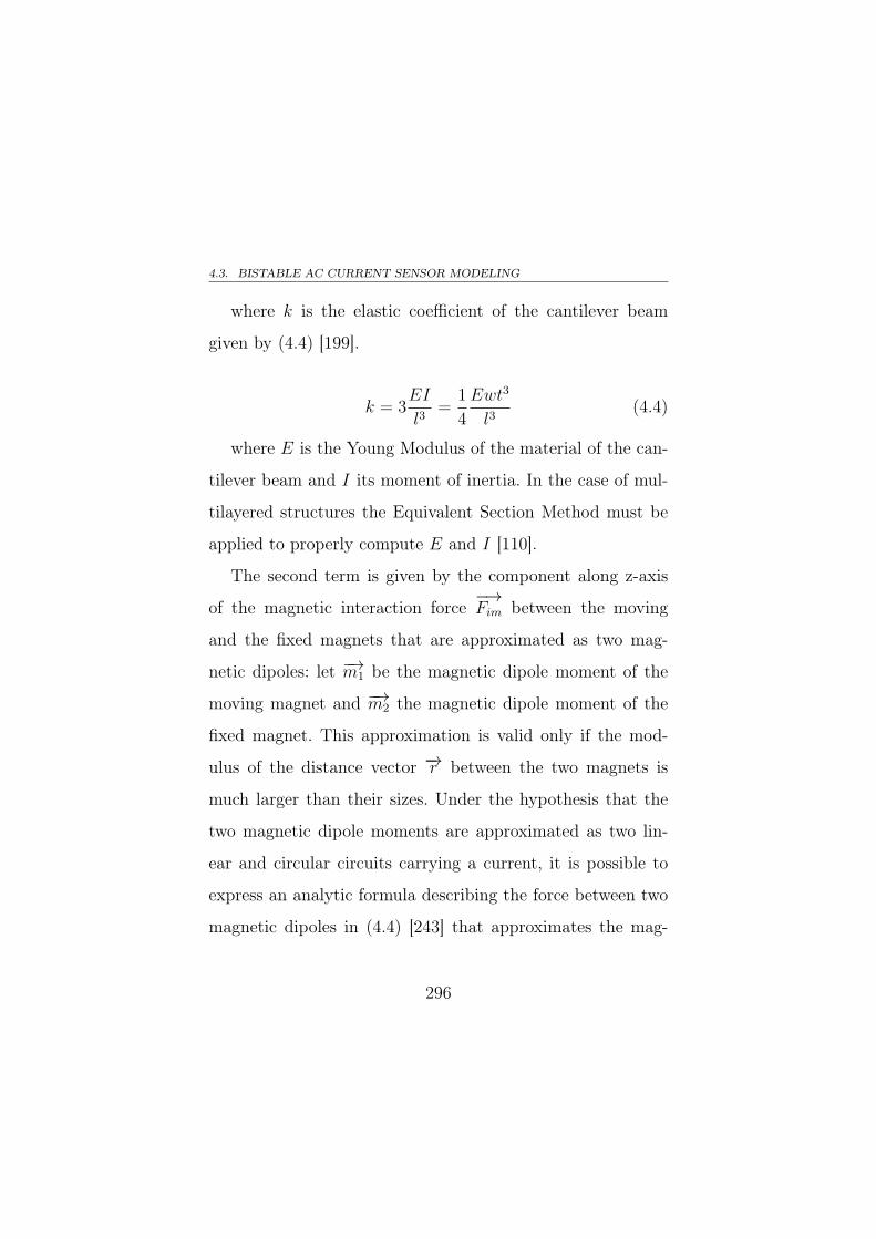
4.3. BISTABLE AC CURRENT SENSOR MODELING
where k is the elastic coefficient of the cantilever beam
given by (4.4) [199].
k = 3EI
l3=
1
4
Ewt3
l3(4.4)
where E is the Young Modulus of the material of the can-
tilever beam and I its moment of inertia. In the case of mul-
tilayered structures the Equivalent Section Method must be
applied to properly compute E and I [110].
The second term is given by the component along z-axis
of the magnetic interaction force−→Fim between the moving
and the fixed magnets that are approximated as two mag-
netic dipoles: let −→m1 be the magnetic dipole moment of the
moving magnet and −→m2 the magnetic dipole moment of the
fixed magnet. This approximation is valid only if the mod-
ulus of the distance vector −→r between the two magnets is
much larger than their sizes. Under the hypothesis that the
two magnetic dipole moments are approximated as two lin-
ear and circular circuits carrying a current, it is possible to
express an analytic formula describing the force between two
magnetic dipoles in (4.4) [243] that approximates the mag-
296
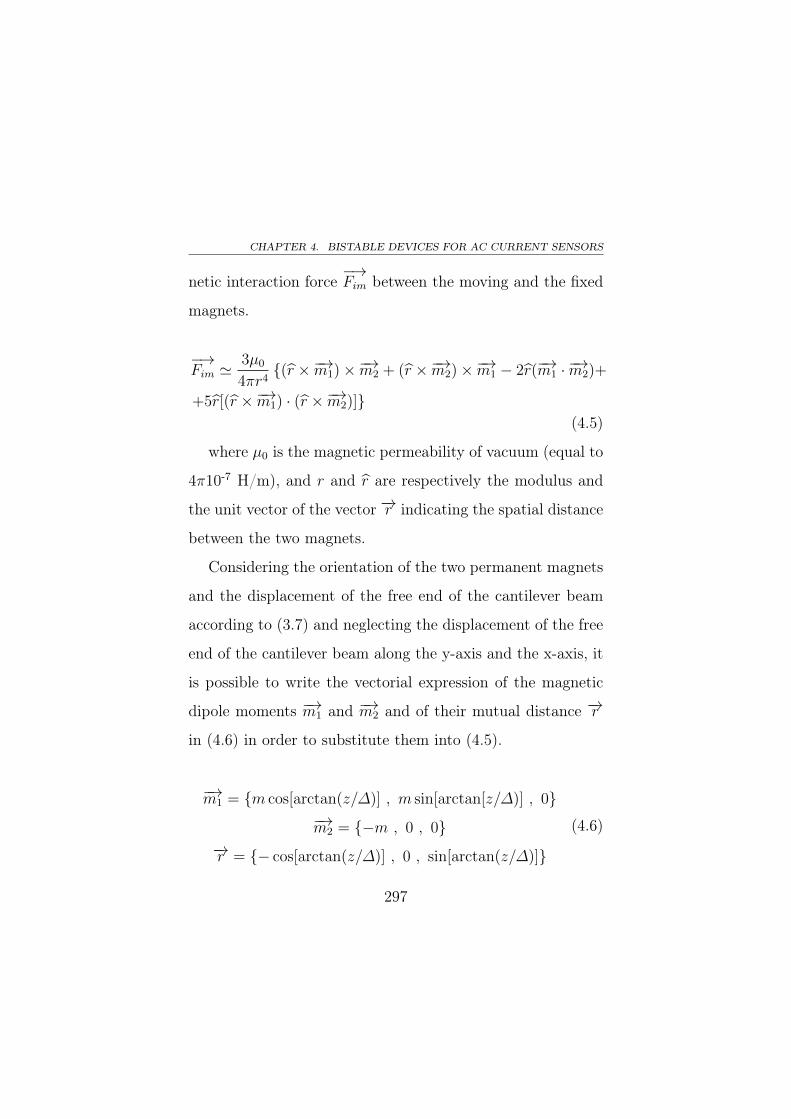
CHAPTER 4. BISTABLE DEVICES FOR AC CURRENT SENSORS
netic interaction force−→Fim between the moving and the fixed
magnets.
−→Fim '
3µ0
4πr4{(r ×−→m1)×−→m2 + (r ×−→m2)×−→m1 − 2r(−→m1 · −→m2)+
+5r[(r ×−→m1) · (r ×−→m2)]}(4.5)
where µ0 is the magnetic permeability of vacuum (equal to
4π10-7 H/m), and r and r are respectively the modulus and
the unit vector of the vector −→r indicating the spatial distance
between the two magnets.
Considering the orientation of the two permanent magnets
and the displacement of the free end of the cantilever beam
according to (3.7) and neglecting the displacement of the free
end of the cantilever beam along the y-axis and the x-axis, it
is possible to write the vectorial expression of the magnetic
dipole moments −→m1 and −→m2 and of their mutual distance −→r
in (4.6) in order to substitute them into (4.5).
−→m1 = {m cos[arctan(z/∆)] , m sin[arctan[z/∆)] , 0}−→m2 = {−m , 0 , 0}
−→r = {− cos[arctan(z/∆)] , 0 , sin[arctan(z/∆)]}
(4.6)
297
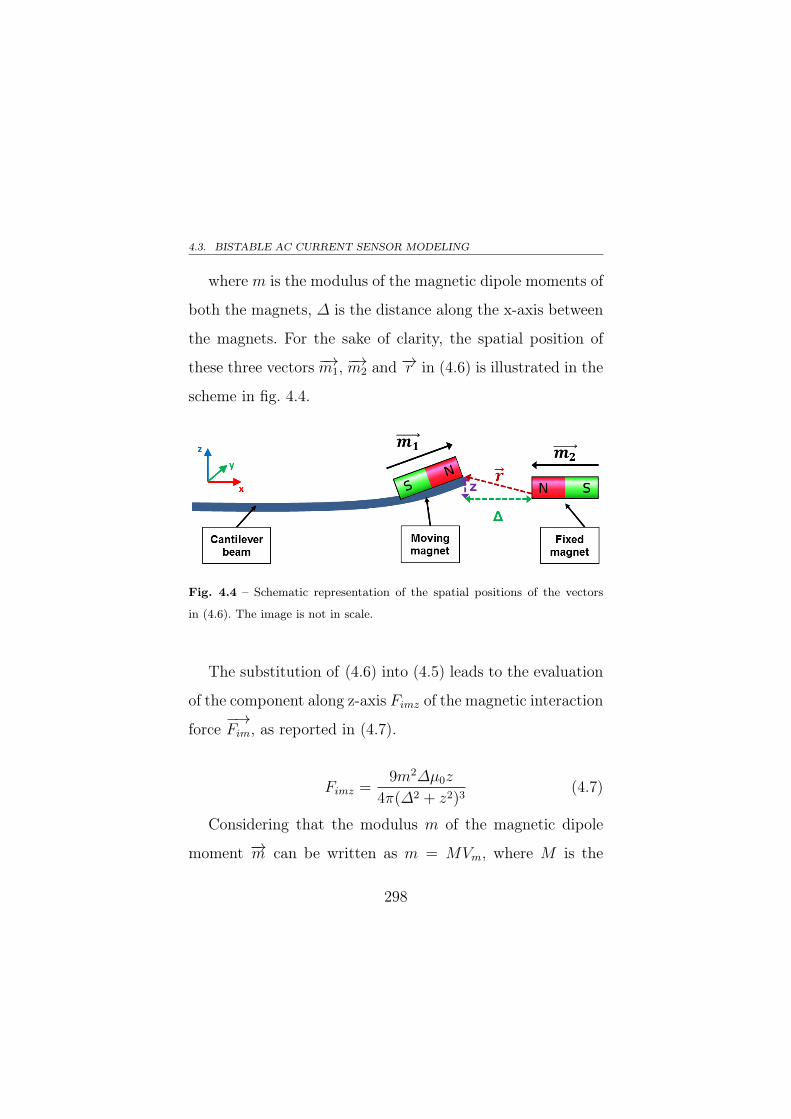
4.3. BISTABLE AC CURRENT SENSOR MODELING
where m is the modulus of the magnetic dipole moments of
both the magnets, ∆ is the distance along the x-axis between
the magnets. For the sake of clarity, the spatial position of
these three vectors −→m1, −→m2 and −→r in (4.6) is illustrated in the
scheme in fig. 4.4.
Fig. 4.4 – Schematic representation of the spatial positions of the vectors
in (4.6). The image is not in scale.
The substitution of (4.6) into (4.5) leads to the evaluation
of the component along z-axis Fimz of the magnetic interaction
force−→Fim, as reported in (4.7).
Fimz =9m2∆µ0z
4π(∆2 + z2)3(4.7)
Considering that the modulus m of the magnetic dipole
moment −→m can be written as m = MVm, where M is the
298
CHAPTER 4. BISTABLE DEVICES FOR AC CURRENT SENSORS
modulus of the magnetization vector−→M [212], and taking into
account that the magnetic remanence Br of the permanent
magnets can be written as Br = µ0M [212], the modulus m
of the magnetic dipole moment can be related to the magnetic
remanence Br of the permanent magnets as in (4.8).
m =BrVmµ0
(4.8)
The substitution of the (4.8) into (4.7) results in (4.9).
Fimz =9Br
2Vm2∆z
4πµ0(∆2 + z2)3(4.9)
By summing and integrating Fkz from (4.9) and Fimz
from (4.3), the expression of the magneto-elastic potential
U(z) in (4.10) is obtained, up to an additive constant.
U(z) =1
2kz2 +
9Br2Vm
2∆
16πµ0(∆2 + z2)2(4.10)
The magneto-elastic potential U(z) in (4.10) exhibits bi-
stable behaviour only if condition in (4.11) is satisfied and in
this case the unstable equilibrium position is in z = 0 and the
two stable equilibrium positions z1,2 are given in (4.12).
299
4.3. BISTABLE AC CURRENT SENSOR MODELING
3
√9
4∆Br
2Vmπµ0k
−∆2 > 0 (4.11)
z1,2 = ±
√√√√ 3
√9
4∆Br
2Vmπµ0k
−∆2 (4.12)
The potential Ug of the gravitational forces is defined
in (4.13) [212].
Ug = −mg(z0 + z) cos(θ) (4.13)
where g is the acceleration of gravity, approximately equal
to 9.81 m/s2, z0 is the “zero-level” assumed for the force of
gravity along the direction of the cantilever beam bending and
θ is the angle between the direction of the cantilever beam dis-
placement z and the direction along which the force of gravity
acts. If cos(θ) is different from zero, the total potential energy
of the system [i.e. U(z) + Ug] will assume different values in
the two stable equilibrium states and the system will have a
larger probability of oscillation around one stable equilibrium
state than around the other one.
300
CHAPTER 4. BISTABLE DEVICES FOR AC CURRENT SENSORS
The input force Fm(t) caused by the interaction of the mag-
netic field of the moving magnet and the magnetic field gener-
ated by the AC current to be measured is given by (4.14) [137].
Fm =
∫d
drHh(t)dVm (4.14)
where Hh(t) is the component on h direction (i.e. the direc-
tion of the minimum distance between the wire carrying the
AC target current and the moving magnet) of the magnetic
field irradiated by the AC electrical current to be measured
and it is defined in (4.15) [137]
Hh(t) =I(t)
2πh(4.15)
where h is the radial distance of the moving magnet from
the wire and I(t) is the AC current to be measured, that is
assumed in the form in (4.16).
I(t) = A sin(2πft) + n(t) (4.16)
where A is the amplitude of the current (the term to be
measured), f is its frequency (equal to 50 Hz or 60 Hz, depend-
301
4.4. BISTABLE AC CURRENT MICROSENSOR IN PIEZOMUMPS®
PROCESS
ing on the countries) and n(t) is the electrical noise carried
by the current.
Through the combination of (4.14), (4.15) and (4.16) and
evaluating the integral in (4.14) (where the integrand is con-
stant with respect to the variable of integration, therefore it is
possible to take it out of the integral significantly simplifying
its calculation), the expression of the input force Fm, acting
along the z-axis, in (4.17) is obtained
Fm = BrVmA sin(2πft) + n(t)
2πh2(4.17)
In (4.17), the distance h is considered larger than the can-
tilever beam tip deflection z and for this reason the influence
of the displacement z is neglected in (4.17).
4.4 Bistable AC current microsensor in
PiezoMUMPs® process
A bistable AC current microsensor has been designed
for a future fabrication in the PiezoMUMPs® process from
MEMSCAPTM.
302
CHAPTER 4. BISTABLE DEVICES FOR AC CURRENT SENSORS
The characteristics, the specifications and the design rules
of the PiezoMUMPs® process are discussed in subsection 2.1.3 [63]
and the model in (4.1) has been taken into account.
The mechanical layer of the cantilever beam is composed of
a n-doped silicon (Si) layer having a thickness t of 10 µm. After
the consideration of several sizes, the length l and the width
w have been designed respectively to 2.5 mm and 900 µm in
order to not exceed with the beam dimensions and to favourite
the deposition by hand of the moving permanent magnet on
the free end of the cantilever beam.
On the silicon layer, a 0.5 µm thick (tPZT ) layer of piezo-
electric aluminium nitride layer (AlN) is deposited by hand
to implement the piezoelectric conversion in the device. The
layer of the AlN has been patterned in order to respect
PiezoMUMPs® design rules [63] and has a length lPZT and a
width wPZT of 2.495 mm and of 890 µm, respectively.
The electrodes of the piezoelectric layer are implemented
by the n-doped mechanical silicon layer in the bottom side,
that also acts as bottom electrode, and by a 1.1 µm thick
aluminium (Al) layer that acts as top electrode. In order to
303
4.4. BISTABLE AC CURRENT MICROSENSOR IN PIEZOMUMPS®
PROCESS
respect PiezoMUMPs® design rules [63], the length le and the
width we of the Al top electrode are respectively 2.492 mm
and of 887 µm. The top electrode is separated into two sub-
electrodes (one on the right side and the other on the left
side separated by a spacing of 10 µm), however, these two
electrodes are connected in short circuit in this device and
considered as a single electrode in this work.
According to this configuration, the device operates in d31
mode.
A 0.2 µm thick silicon dioxide layer has been used as electri-
cally isolating layer to separate conductive layers, implement-
ing top and bottom electrodes, in the routing of the piezo
stack.
At the free end of the cantilever beam, a silicon (Si) me-
chanical proof mass is attached (on its bottom side) in or-
der to increase the device sensitivity to both the external
magnetic force Fm(t) and the acceleration from the mechan-
ical noise aext(t) by providing a larger value of the mass m
in (4.1). The proof mass is composed of the SOI substrate of
the PiezoMUMPs® process and has a length of 695 µm, a
304
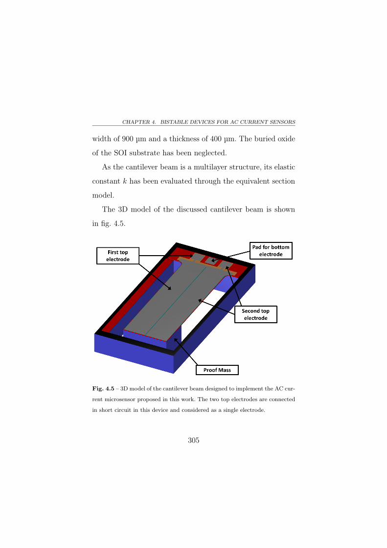
CHAPTER 4. BISTABLE DEVICES FOR AC CURRENT SENSORS
width of 900 µm and a thickness of 400 µm. The buried oxide
of the SOI substrate has been neglected.
As the cantilever beam is a multilayer structure, its elastic
constant k has been evaluated through the equivalent section
model.
The 3D model of the discussed cantilever beam is shown
in fig. 4.5.
Fig. 4.5 – 3D model of the cantilever beam designed to implement the AC cur-
rent microsensor proposed in this work. The two top electrodes are connected
in short circuit in this device and considered as a single electrode.
305
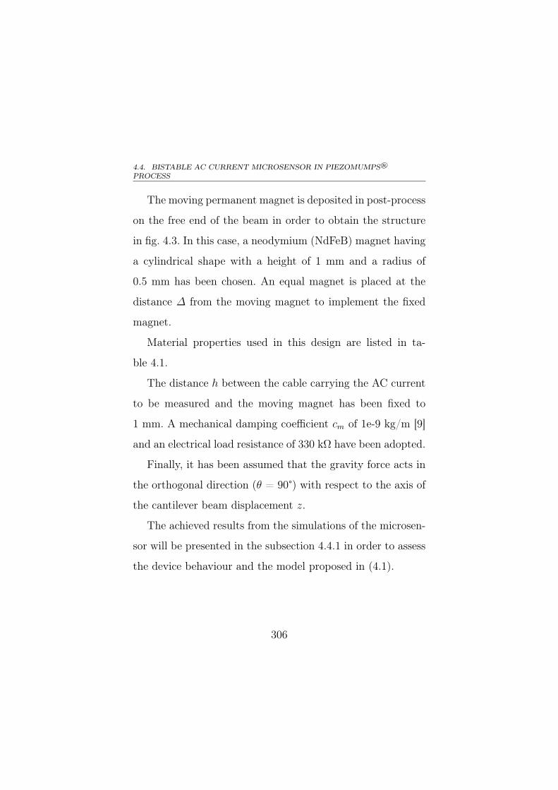
4.4. BISTABLE AC CURRENT MICROSENSOR IN PIEZOMUMPS®
PROCESS
The moving permanent magnet is deposited in post-process
on the free end of the beam in order to obtain the structure
in fig. 4.3. In this case, a neodymium (NdFeB) magnet having
a cylindrical shape with a height of 1 mm and a radius of
0.5 mm has been chosen. An equal magnet is placed at the
distance ∆ from the moving magnet to implement the fixed
magnet.
Material properties used in this design are listed in ta-
ble 4.1.
The distance h between the cable carrying the AC current
to be measured and the moving magnet has been fixed to
1 mm. A mechanical damping coefficient cm of 1e-9 kg/m [9]
and an electrical load resistance of 330 kΩ have been adopted.
Finally, it has been assumed that the gravity force acts in
the orthogonal direction (θ = 90°) with respect to the axis of
the cantilever beam displacement z.
The achieved results from the simulations of the microsen-
sor will be presented in the subsection 4.4.1 in order to assess
the device behaviour and the model proposed in (4.1).
306
CHAPTER 4. BISTABLE DEVICES FOR AC CURRENT SENSORS
Table 4.1 – Material properties used in the design and simulations of the AC
microsensor [213].
Properties Values for Si
Mass density 2329 kg/m3
Young Modulus 170 GPa
Values for AlN
Mass density 3260 kg/m3
Young Modulus in 33 direction 410 GPa
Piezoelectric coupling in 31 direction e31 -0.58 C/m2
Electrical permittivity in 33 direction ε33 7.97 pF/m
Values for Al
Mass density 2700 kg/m3
Young Modulus 70 GPa
Values for NdFeB
Mass density 7400 kg/m3
Magnetic remanence Br 1170 mT [187]
4.4.1 Device simulations
The model of the device in (4.1), along with the parame-
ter values presented in section 4.4, has been simulated in the
Simulink® environment of Matlab® platform.
The aim is to assess, through the validation of the device
model, that a bistable system can achieve better performance
307
4.4. BISTABLE AC CURRENT MICROSENSOR IN PIEZOMUMPS®
PROCESS
than a linear resonant system in terms of sensing capabilities
(in certain operating conditions) and energy harvested.
Design of the distance between permanent magnets
After the consideration of the device model in (4.1) and
the examination of the given parameter values in section 4.4,
the distance ∆ between permanent magnets must be defined.
The application of those parameter values to (4.11) leads to
a limit value of ∆ = 3.32 mm in order to achieve bistable
behaviour: for values of ∆ smaller than 3.32 mm, the system
exhibits bistable behaviour, for larger distances linear reso-
nant behaviour is expected. This means that the distance ∆
plays a crucial role in the device operation.
In fact, in the bistable operative range (∆ ≤ 3.32 mm),
taking into account (4.10), different values of the parameter
∆ result in bistable magneto-elastic potentials U(z) having
distinct shapes, as shown in the plot in fig. 4.6 for four different
values of the distance ∆ (2.1 mm, 2.2 mm, 2.25 mm, 2.3 mm).
In particular, since the distance ∆ affects the magnetic
levitation force between permanent magnets, higher values
of ∆ in the bistable operative range lead to smaller inter-
308
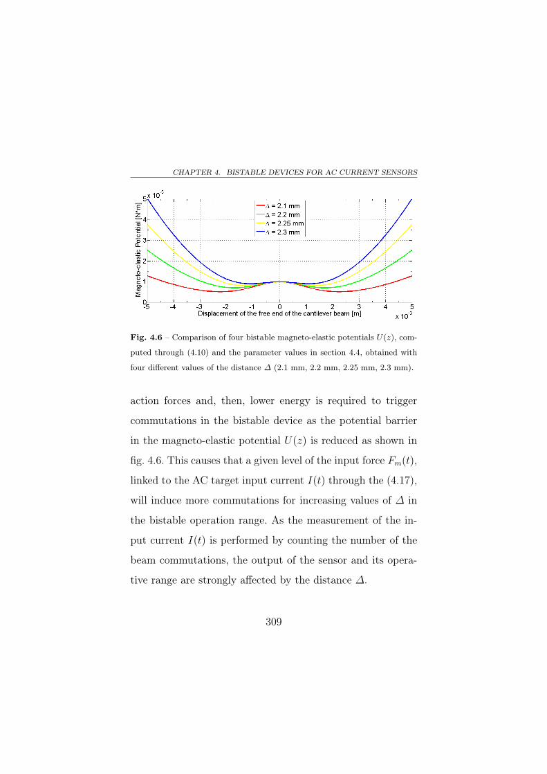
CHAPTER 4. BISTABLE DEVICES FOR AC CURRENT SENSORS
Fig. 4.6 – Comparison of four bistable magneto-elastic potentials U(z), com-
puted through (4.10) and the parameter values in section 4.4, obtained with
four different values of the distance ∆ (2.1 mm, 2.2 mm, 2.25 mm, 2.3 mm).
action forces and, then, lower energy is required to trigger
commutations in the bistable device as the potential barrier
in the magneto-elastic potential U(z) is reduced as shown in
fig. 4.6. This causes that a given level of the input force Fm(t),
linked to the AC target input current I(t) through the (4.17),
will induce more commutations for increasing values of ∆ in
the bistable operation range. As the measurement of the in-
put current I(t) is performed by counting the number of the
beam commutations, the output of the sensor and its opera-
tive range are strongly affected by the distance ∆.
309
4.4. BISTABLE AC CURRENT MICROSENSOR IN PIEZOMUMPS®
PROCESS
Accurate attention should also be paid to the level of input
mechanical noise: In fact, the ranges of the acceleration aext in-
duced by mechanical noise and its effect on the bistable system
(given its magneto-elastic bistable potential) must be investi-
gated. If an energy harvesting application must be addressed,
external noise should be enough to guarantee the presence
of beam switchings (i.e. high energy orbits behaviour). In
this sensing application, however, the measurement of the un-
known quantity is performed by counting of the number of
beam commutations; therefore, it is evident that commuta-
tions triggered by mechanical noise cannot be counted in the
evaluation of the target current.
For this reason, in the designing of the distance ∆, first of
all, it is necessary to verify the minimum and the maximum
amplitude of the AC current that the sensor is able to de-
tect and, then, the maximum level of vibrational noise should
be investigated to avoid device commutations induced by the
input vibrational acceleration.
310
CHAPTER 4. BISTABLE DEVICES FOR AC CURRENT SENSORS
Model simulations
Before running the simulations of the device, the specifica-
tions of the system inputs have been investigated. Given the
sizes of the microstructure, external accelerations aext having
a Root Mean Square (RMS) value smaller than 1g have been
considered to speed up and simplify the design.
The input mechanical noise aext has been modeled through
a band-limited white noise with a given gain to regulate its
RMS value and filtered by a eighth-order Butterworth low-
pass filter having a cut-off frequency of 500 Hz.
Examples of the time series of the input acceleration aext
and its Power Spectrum Density (PSD) are shown in figs. 4.7–
4.12 for three distinct RMS values of the input acceleration
(0.031g, 0.31g and 0.98g).
Considering as input several AC current magnitudes with-
out electrical noise n(t) = 0, several levels of input mechani-
cal noise aext and the parameters described in section 4.4, the
system in (4.1) has been numerically simulated in Simulink®
using Runge-Kutta “ODE45” integration formula [44]. As re-
sults of simulations, the number of commutations between the
311
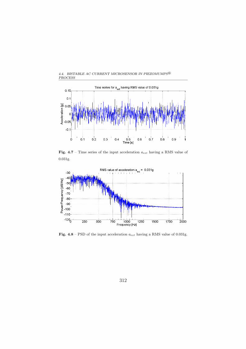
4.4. BISTABLE AC CURRENT MICROSENSOR IN PIEZOMUMPS®
PROCESS
Fig. 4.7 – Time series of the input acceleration aext having a RMS value of
0.031g.
Fig. 4.8 – PSD of the input acceleration aext having a RMS value of 0.031g.
312
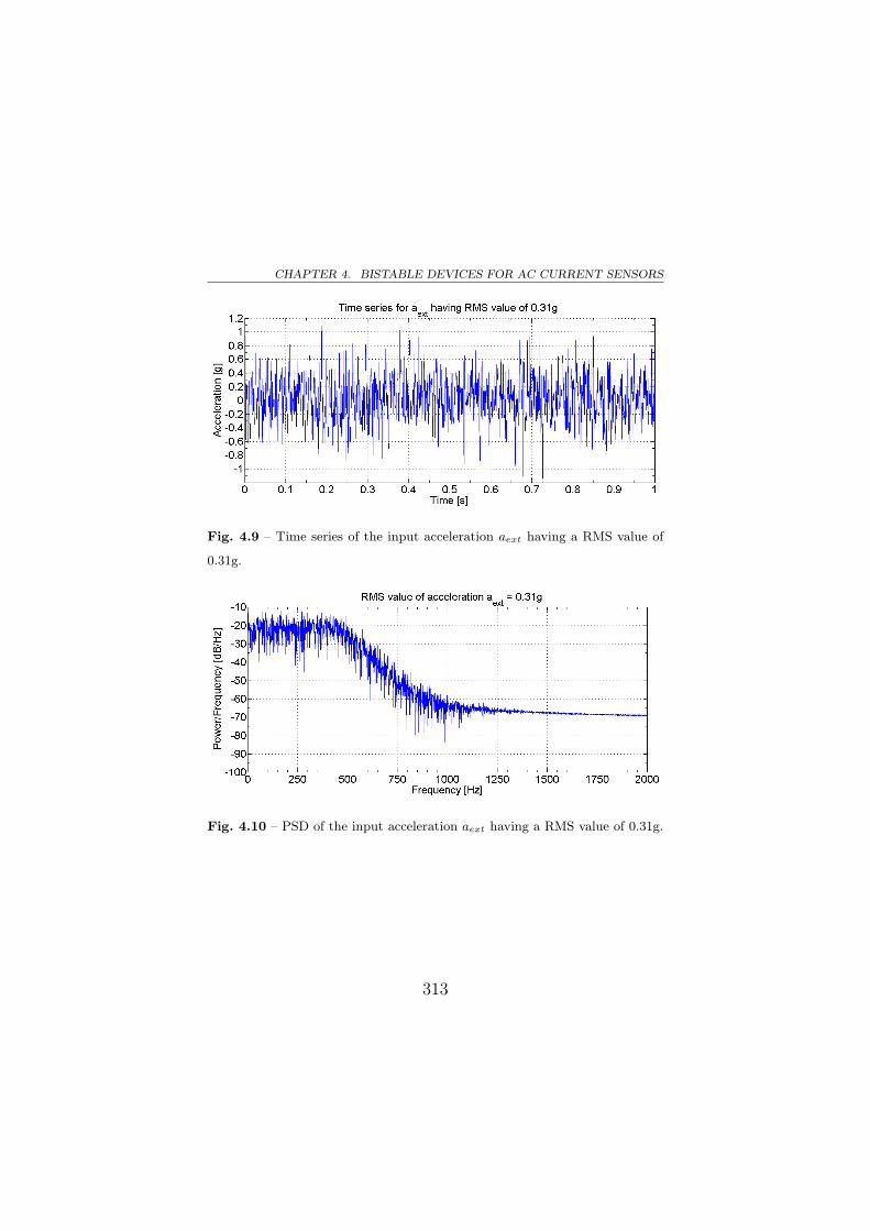
CHAPTER 4. BISTABLE DEVICES FOR AC CURRENT SENSORS
Fig. 4.9 – Time series of the input acceleration aext having a RMS value of
0.31g.
Fig. 4.10 – PSD of the input acceleration aext having a RMS value of 0.31g.
313
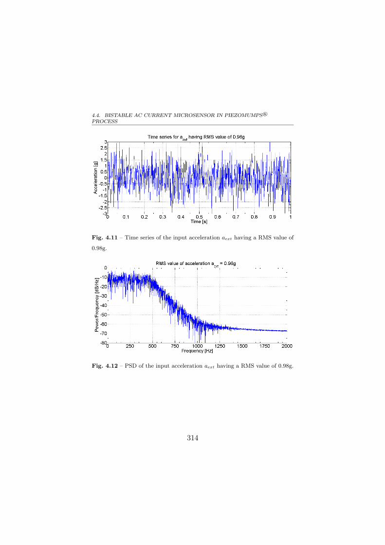
4.4. BISTABLE AC CURRENT MICROSENSOR IN PIEZOMUMPS®
PROCESS
Fig. 4.11 – Time series of the input acceleration aext having a RMS value of
0.98g.
Fig. 4.12 – PSD of the input acceleration aext having a RMS value of 0.98g.
314
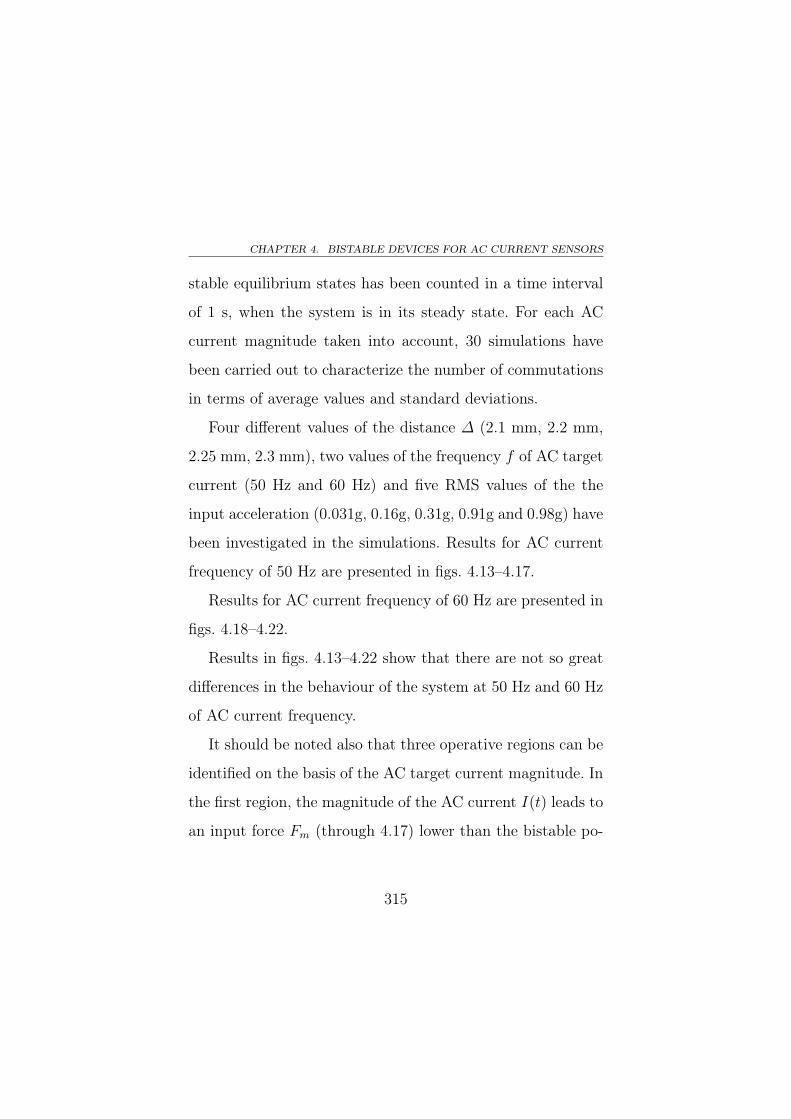
CHAPTER 4. BISTABLE DEVICES FOR AC CURRENT SENSORS
stable equilibrium states has been counted in a time interval
of 1 s, when the system is in its steady state. For each AC
current magnitude taken into account, 30 simulations have
been carried out to characterize the number of commutations
in terms of average values and standard deviations.
Four different values of the distance ∆ (2.1 mm, 2.2 mm,
2.25 mm, 2.3 mm), two values of the frequency f of AC target
current (50 Hz and 60 Hz) and five RMS values of the the
input acceleration (0.031g, 0.16g, 0.31g, 0.91g and 0.98g) have
been investigated in the simulations. Results for AC current
frequency of 50 Hz are presented in figs. 4.13–4.17.
Results for AC current frequency of 60 Hz are presented in
figs. 4.18–4.22.
Results in figs. 4.13–4.22 show that there are not so great
differences in the behaviour of the system at 50 Hz and 60 Hz
of AC current frequency.
It should be noted also that three operative regions can be
identified on the basis of the AC target current magnitude. In
the first region, the magnitude of the AC current I(t) leads to
an input force Fm (through 4.17) lower than the bistable po-
315
4.4. BISTABLE AC CURRENT MICROSENSOR IN PIEZOMUMPS®
PROCESS
Fig. 4.13 – Mean number of commutations in 1 s, over 30 simulations, versus
AC current magnitude at a frequency of 50 Hz, when the RMS value of input
acceleration aext is 0.031g, for four values of the distance ∆ (2.1 mm, 2.2 mm,
2.25 mm, 2.3 mm).
tential barrier; in this case, the system oscillates only around
one of its stable equilibrium states or exhibits some commu-
tations induced by the external mechanical noise aext; this
region can be named “subthreshold” region. In the second re-
gion, the level of the force Fm generated by the AC target
current is able to put the system in commutation between its
stable equilibrium states and the number of commutations in-
creases when the AC current magnitude grows and the level of
mechanical noise is fixed: in this case the system can be used
316
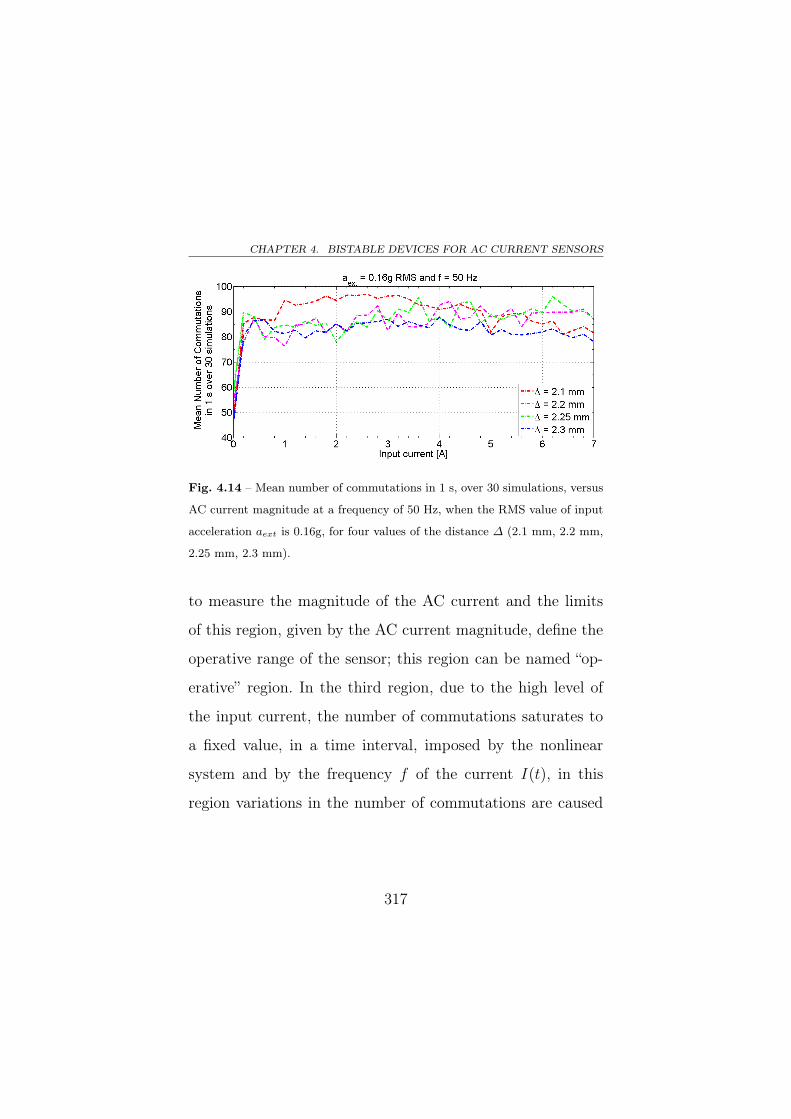
CHAPTER 4. BISTABLE DEVICES FOR AC CURRENT SENSORS
Fig. 4.14 – Mean number of commutations in 1 s, over 30 simulations, versus
AC current magnitude at a frequency of 50 Hz, when the RMS value of input
acceleration aext is 0.16g, for four values of the distance ∆ (2.1 mm, 2.2 mm,
2.25 mm, 2.3 mm).
to measure the magnitude of the AC current and the limits
of this region, given by the AC current magnitude, define the
operative range of the sensor; this region can be named “op-
erative” region. In the third region, due to the high level of
the input current, the number of commutations saturates to
a fixed value, in a time interval, imposed by the nonlinear
system and by the frequency f of the current I(t), in this
region variations in the number of commutations are caused
317
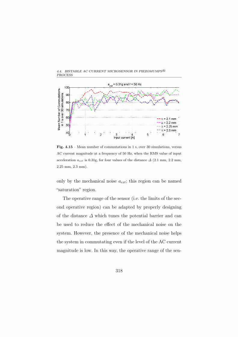
4.4. BISTABLE AC CURRENT MICROSENSOR IN PIEZOMUMPS®
PROCESS
Fig. 4.15 – Mean number of commutations in 1 s, over 30 simulations, versus
AC current magnitude at a frequency of 50 Hz, when the RMS value of input
acceleration aext is 0.31g, for four values of the distance ∆ (2.1 mm, 2.2 mm,
2.25 mm, 2.3 mm).
only by the mechanical noise aext; this region can be named
“saturation” region.
The operative range of the sensor (i.e. the limits of the sec-
ond operative region) can be adapted by properly designing
of the distance ∆ which tunes the potential barrier and can
be used to reduce the effect of the mechanical noise on the
system. However, the presence of the mechanical noise helps
the system in commutating even if the level of the AC current
magnitude is low. In this way, the operative range of the sen-
318
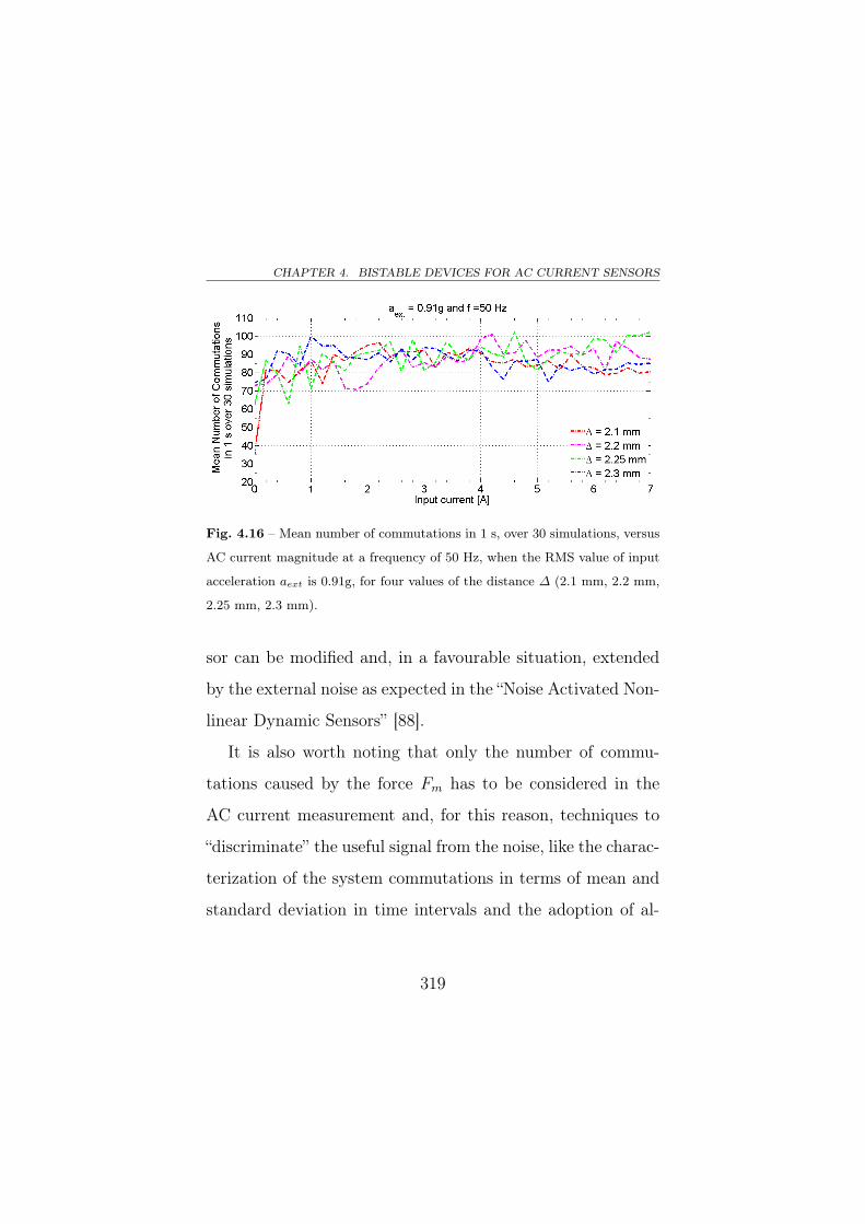
CHAPTER 4. BISTABLE DEVICES FOR AC CURRENT SENSORS
Fig. 4.16 – Mean number of commutations in 1 s, over 30 simulations, versus
AC current magnitude at a frequency of 50 Hz, when the RMS value of input
acceleration aext is 0.91g, for four values of the distance ∆ (2.1 mm, 2.2 mm,
2.25 mm, 2.3 mm).
sor can be modified and, in a favourable situation, extended
by the external noise as expected in the “Noise Activated Non-
linear Dynamic Sensors” [88].
It is also worth noting that only the number of commu-
tations caused by the force Fm has to be considered in the
AC current measurement and, for this reason, techniques to
“discriminate” the useful signal from the noise, like the charac-
terization of the system commutations in terms of mean and
standard deviation in time intervals and the adoption of al-
319
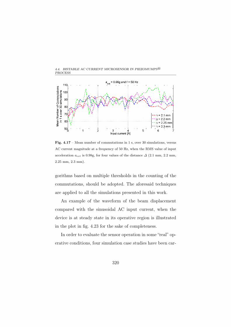
4.4. BISTABLE AC CURRENT MICROSENSOR IN PIEZOMUMPS®
PROCESS
Fig. 4.17 – Mean number of commutations in 1 s, over 30 simulations, versus
AC current magnitude at a frequency of 50 Hz, when the RMS value of input
acceleration aext is 0.98g, for four values of the distance ∆ (2.1 mm, 2.2 mm,
2.25 mm, 2.3 mm).
gorithms based on multiple thresholds in the counting of the
commutations, should be adopted. The aforesaid techniques
are applied to all the simulations presented in this work.
An example of the waveform of the beam displacement
compared with the sinusoidal AC input current, when the
device is at steady state in its operative region is illustrated
in the plot in fig. 4.23 for the sake of completeness.
In order to evaluate the sensor operation in some “real” op-
erative conditions, four simulation case studies have been car-
320
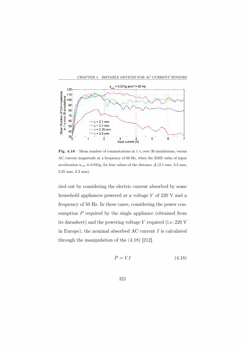
CHAPTER 4. BISTABLE DEVICES FOR AC CURRENT SENSORS
Fig. 4.18 – Mean number of commutations in 1 s, over 30 simulations, versus
AC current magnitude at a frequency of 60 Hz, when the RMS value of input
acceleration aext is 0.031g, for four values of the distance ∆ (2.1 mm, 2.2 mm,
2.25 mm, 2.3 mm).
ried out by considering the electric current absorbed by some
household appliances powered at a voltage V of 220 V and a
frequency of 50 Hz. In these cases, considering the power con-
sumption P required by the single appliance (obtained from
its datasheet) and the powering voltage V required (i.e. 220 V
in Europe), the nominal absorbed AC current I is calculated
through the manipulation of the (4.18) [212].
P = V I (4.18)
321
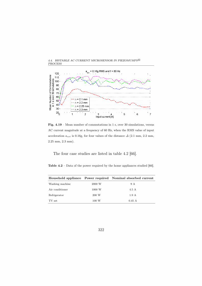
4.4. BISTABLE AC CURRENT MICROSENSOR IN PIEZOMUMPS®
PROCESS
Fig. 4.19 – Mean number of commutations in 1 s, over 30 simulations, versus
AC current magnitude at a frequency of 60 Hz, when the RMS value of input
acceleration aext is 0.16g, for four values of the distance ∆ (2.1 mm, 2.2 mm,
2.25 mm, 2.3 mm).
The four case studies are listed in table 4.2 [66].
Table 4.2 – Data of the power required by the home appliances studied [66].
Household appliance Power required Nominal absorbed current
Washing machine 2000 W 9 A
Air conditioner 1000 W 4.5 A
Refrigerator 200 W 1.9 A
TV set 100 W 0.45 A
322
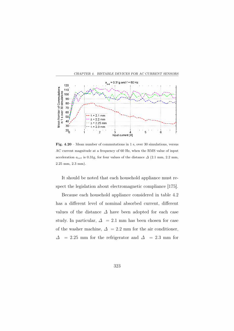
CHAPTER 4. BISTABLE DEVICES FOR AC CURRENT SENSORS
Fig. 4.20 – Mean number of commutations in 1 s, over 30 simulations, versus
AC current magnitude at a frequency of 60 Hz, when the RMS value of input
acceleration aext is 0.31g, for four values of the distance ∆ (2.1 mm, 2.2 mm,
2.25 mm, 2.3 mm).
It should be noted that each household appliance must re-
spect the legislation about electromagnetic compliance [175].
Because each household appliance considered in table 4.2
has a different level of nominal absorbed current, different
values of the distance ∆ have been adopted for each case
study. In particular, ∆ = 2.1 mm has been chosen for case
of the washer machine, ∆ = 2.2 mm for the air conditioner,
∆ = 2.25 mm for the refrigerator and ∆ = 2.3 mm for
323
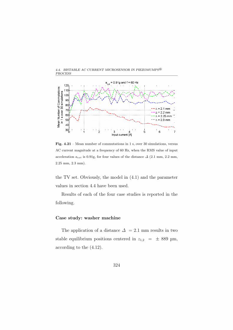
4.4. BISTABLE AC CURRENT MICROSENSOR IN PIEZOMUMPS®
PROCESS
Fig. 4.21 – Mean number of commutations in 1 s, over 30 simulations, versus
AC current magnitude at a frequency of 60 Hz, when the RMS value of input
acceleration aext is 0.91g, for four values of the distance ∆ (2.1 mm, 2.2 mm,
2.25 mm, 2.3 mm).
the TV set. Obviously, the model in (4.1) and the parameter
values in section 4.4 have been used.
Results of each of the four case studies is reported in the
following.
Case study: washer machine
The application of a distance ∆ = 2.1 mm results in two
stable equilibrium positions centered in z1,2 = ± 889 µm,
according to the (4.12).
324
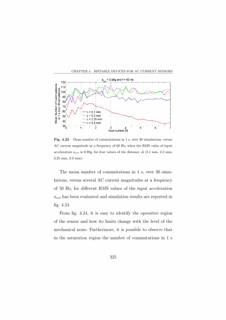
CHAPTER 4. BISTABLE DEVICES FOR AC CURRENT SENSORS
Fig. 4.22 – Mean number of commutations in 1 s, over 30 simulations, versus
AC current magnitude at a frequency of 60 Hz, when the RMS value of input
acceleration aext is 0.98g, for four values of the distance ∆ (2.1 mm, 2.2 mm,
2.25 mm, 2.3 mm).
The mean number of commutations in 1 s, over 30 simu-
lations, versus several AC current magnitudes at a frequency
of 50 Hz, for different RMS values of the input acceleration
aext has been evaluated and simulation results are reported in
fig. 4.24
From fig. 4.24, it is easy to identify the operative region
of the sensor and how its limits change with the level of the
mechanical noise. Furthermore, it is possible to observe that
in the saturation region the number of commutations in 1 s
325
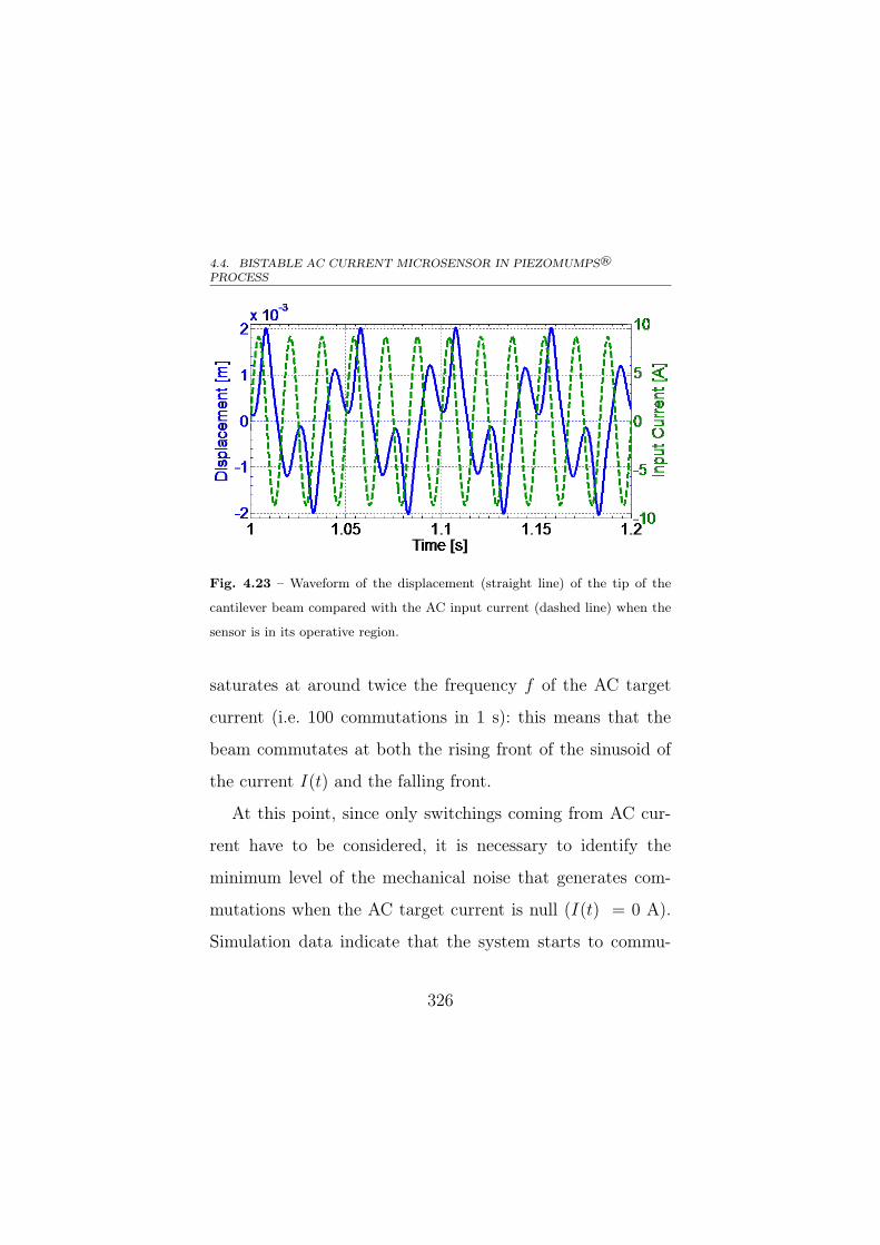
4.4. BISTABLE AC CURRENT MICROSENSOR IN PIEZOMUMPS®
PROCESS
Fig. 4.23 – Waveform of the displacement (straight line) of the tip of the
cantilever beam compared with the AC input current (dashed line) when the
sensor is in its operative region.
saturates at around twice the frequency f of the AC target
current (i.e. 100 commutations in 1 s): this means that the
beam commutates at both the rising front of the sinusoid of
the current I(t) and the falling front.
At this point, since only switchings coming from AC cur-
rent have to be considered, it is necessary to identify the
minimum level of the mechanical noise that generates com-
mutations when the AC target current is null (I(t) = 0 A).
Simulation data indicate that the system starts to commu-
326
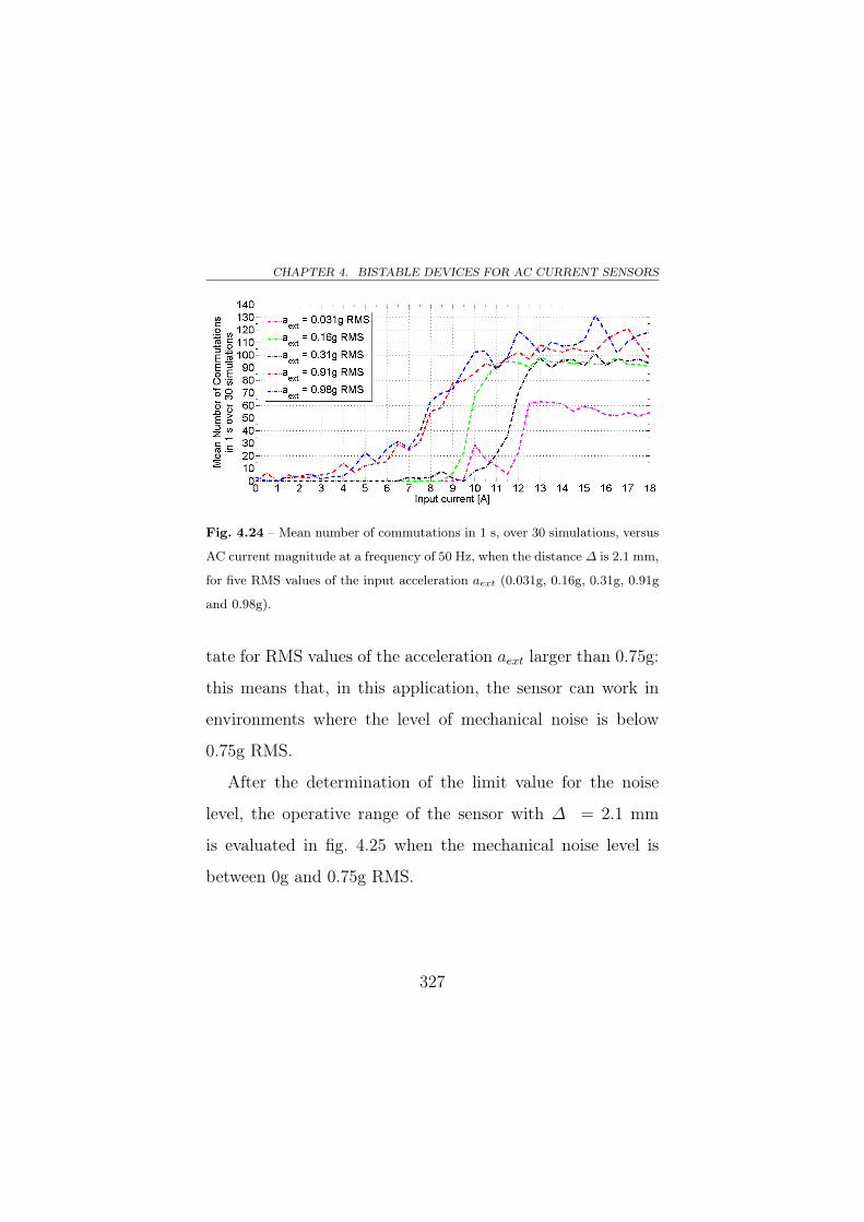
CHAPTER 4. BISTABLE DEVICES FOR AC CURRENT SENSORS
Fig. 4.24 – Mean number of commutations in 1 s, over 30 simulations, versus
AC current magnitude at a frequency of 50 Hz, when the distance ∆ is 2.1 mm,
for five RMS values of the input acceleration aext (0.031g, 0.16g, 0.31g, 0.91g
and 0.98g).
tate for RMS values of the acceleration aext larger than 0.75g:
this means that, in this application, the sensor can work in
environments where the level of mechanical noise is below
0.75g RMS.
After the determination of the limit value for the noise
level, the operative range of the sensor with ∆ = 2.1 mm
is evaluated in fig. 4.25 when the mechanical noise level is
between 0g and 0.75g RMS.
327

4.4. BISTABLE AC CURRENT MICROSENSOR IN PIEZOMUMPS®
PROCESS
Fig. 4.25 – Mean number of commutations and standard deviation in 1 s,
over 30 simulations, versus AC current magnitude at a frequency of 50 Hz,
when the distance ∆ is 2.1 mm and the input acceleration aext is between 0g
and 0.75g RMS.
From fig. 4.25 it is possible to state that the system can
detect AC currents magnitudes between 4.75 A and 9 A (with
a reduction of sensitivity around 9 A for high levels of noise),
according to the range of absorbed currents by the washer
machine.
RMS values of the displacement of the beam and of the
voltage output from the piezoelectric layer of the device (i.e.
the energy harvested by the system), for different AC cur-
328
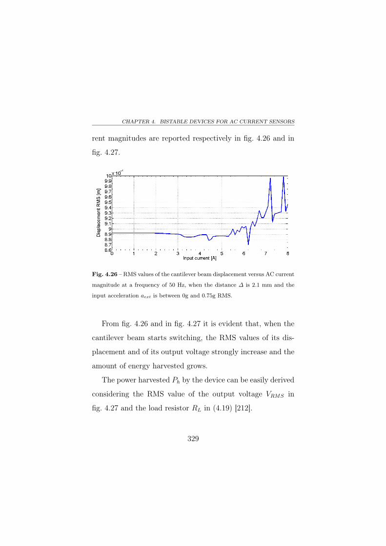
CHAPTER 4. BISTABLE DEVICES FOR AC CURRENT SENSORS
rent magnitudes are reported respectively in fig. 4.26 and in
fig. 4.27.
Fig. 4.26 – RMS values of the cantilever beam displacement versus AC current
magnitude at a frequency of 50 Hz, when the distance ∆ is 2.1 mm and the
input acceleration aext is between 0g and 0.75g RMS.
From fig. 4.26 and in fig. 4.27 it is evident that, when the
cantilever beam starts switching, the RMS values of its dis-
placement and of its output voltage strongly increase and the
amount of energy harvested grows.
The power harvested Ph by the device can be easily derived
considering the RMS value of the output voltage VRMS in
fig. 4.27 and the load resistor RL in (4.19) [212].
329
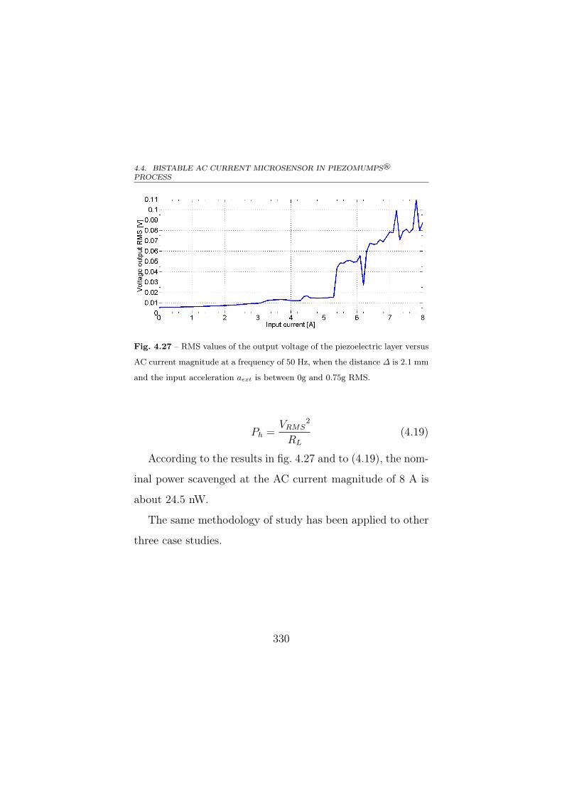
4.4. BISTABLE AC CURRENT MICROSENSOR IN PIEZOMUMPS®
PROCESS
Fig. 4.27 – RMS values of the output voltage of the piezoelectric layer versus
AC current magnitude at a frequency of 50 Hz, when the distance ∆ is 2.1 mm
and the input acceleration aext is between 0g and 0.75g RMS.
Ph =VRMS
2
RL
(4.19)
According to the results in fig. 4.27 and to (4.19), the nom-
inal power scavenged at the AC current magnitude of 8 A is
about 24.5 nW.
The same methodology of study has been applied to other
three case studies.
330
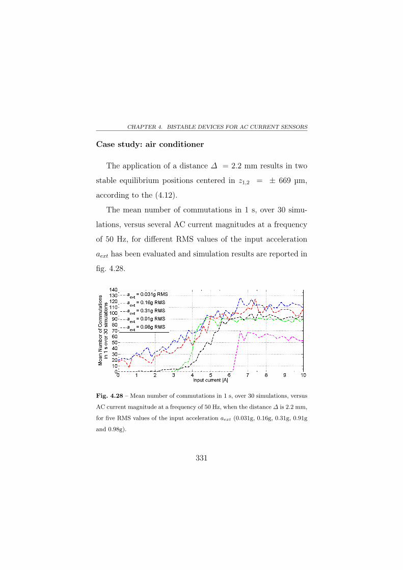
CHAPTER 4. BISTABLE DEVICES FOR AC CURRENT SENSORS
Case study: air conditioner
The application of a distance ∆ = 2.2 mm results in two
stable equilibrium positions centered in z1,2 = ± 669 µm,
according to the (4.12).
The mean number of commutations in 1 s, over 30 simu-
lations, versus several AC current magnitudes at a frequency
of 50 Hz, for different RMS values of the input acceleration
aext has been evaluated and simulation results are reported in
fig. 4.28.
Fig. 4.28 – Mean number of commutations in 1 s, over 30 simulations, versus
AC current magnitude at a frequency of 50 Hz, when the distance ∆ is 2.2 mm,
for five RMS values of the input acceleration aext (0.031g, 0.16g, 0.31g, 0.91g
and 0.98g).
331
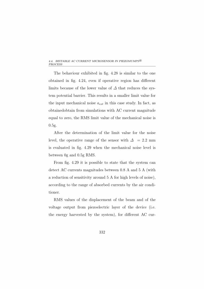
4.4. BISTABLE AC CURRENT MICROSENSOR IN PIEZOMUMPS®
PROCESS
The behaviour exhibited in fig. 4.28 is similar to the one
obtained in fig. 4.24, even if operative region has different
limits because of the lower value of ∆ that reduces the sys-
tem potential barrier. This results in a smaller limit value for
the input mechanical noise aext in this case study. In fact, as
obtainedobtain from simulations with AC current magnitude
equal to zero, the RMS limit value of the mechanical noise is
0.5g.
After the determination of the limit value for the noise
level, the operative range of the sensor with ∆ = 2.2 mm
is evaluated in fig. 4.29 when the mechanical noise level is
between 0g and 0.5g RMS.
From fig. 4.29 it is possible to state that the system can
detect AC currents magnitudes between 0.8 A and 5 A (with
a reduction of sensitivity around 5 A for high levels of noise),
according to the range of absorbed currents by the air condi-
tioner.
RMS values of the displacement of the beam and of the
voltage output from piezoelectric layer of the device (i.e.
the energy harvested by the system), for different AC cur-
332
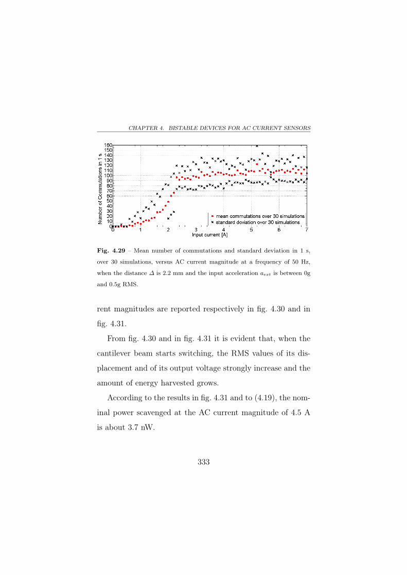
CHAPTER 4. BISTABLE DEVICES FOR AC CURRENT SENSORS
Fig. 4.29 – Mean number of commutations and standard deviation in 1 s,
over 30 simulations, versus AC current magnitude at a frequency of 50 Hz,
when the distance ∆ is 2.2 mm and the input acceleration aext is between 0g
and 0.5g RMS.
rent magnitudes are reported respectively in fig. 4.30 and in
fig. 4.31.
From fig. 4.30 and in fig. 4.31 it is evident that, when the
cantilever beam starts switching, the RMS values of its dis-
placement and of its output voltage strongly increase and the
amount of energy harvested grows.
According to the results in fig. 4.31 and to (4.19), the nom-
inal power scavenged at the AC current magnitude of 4.5 A
is about 3.7 nW.
333
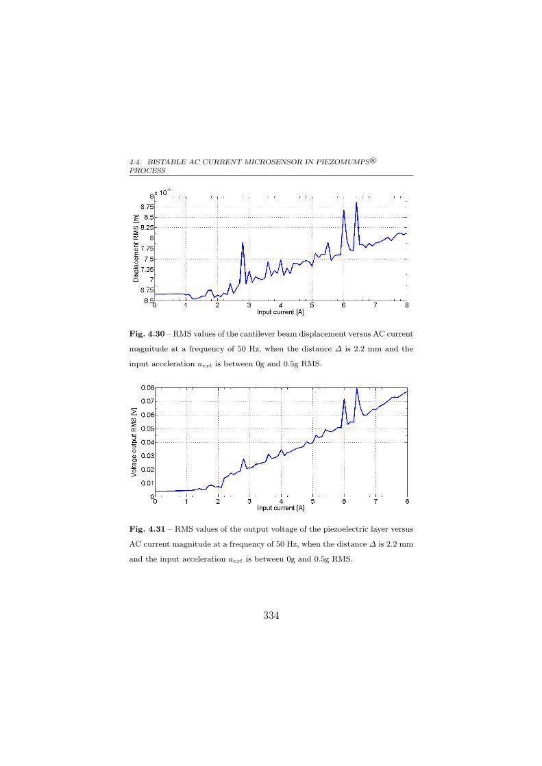
4.4. BISTABLE AC CURRENT MICROSENSOR IN PIEZOMUMPS®
PROCESS
Fig. 4.30 – RMS values of the cantilever beam displacement versus AC current
magnitude at a frequency of 50 Hz, when the distance ∆ is 2.2 mm and the
input acceleration aext is between 0g and 0.5g RMS.
Fig. 4.31 – RMS values of the output voltage of the piezoelectric layer versus
AC current magnitude at a frequency of 50 Hz, when the distance ∆ is 2.2 mm
and the input acceleration aext is between 0g and 0.5g RMS.
334
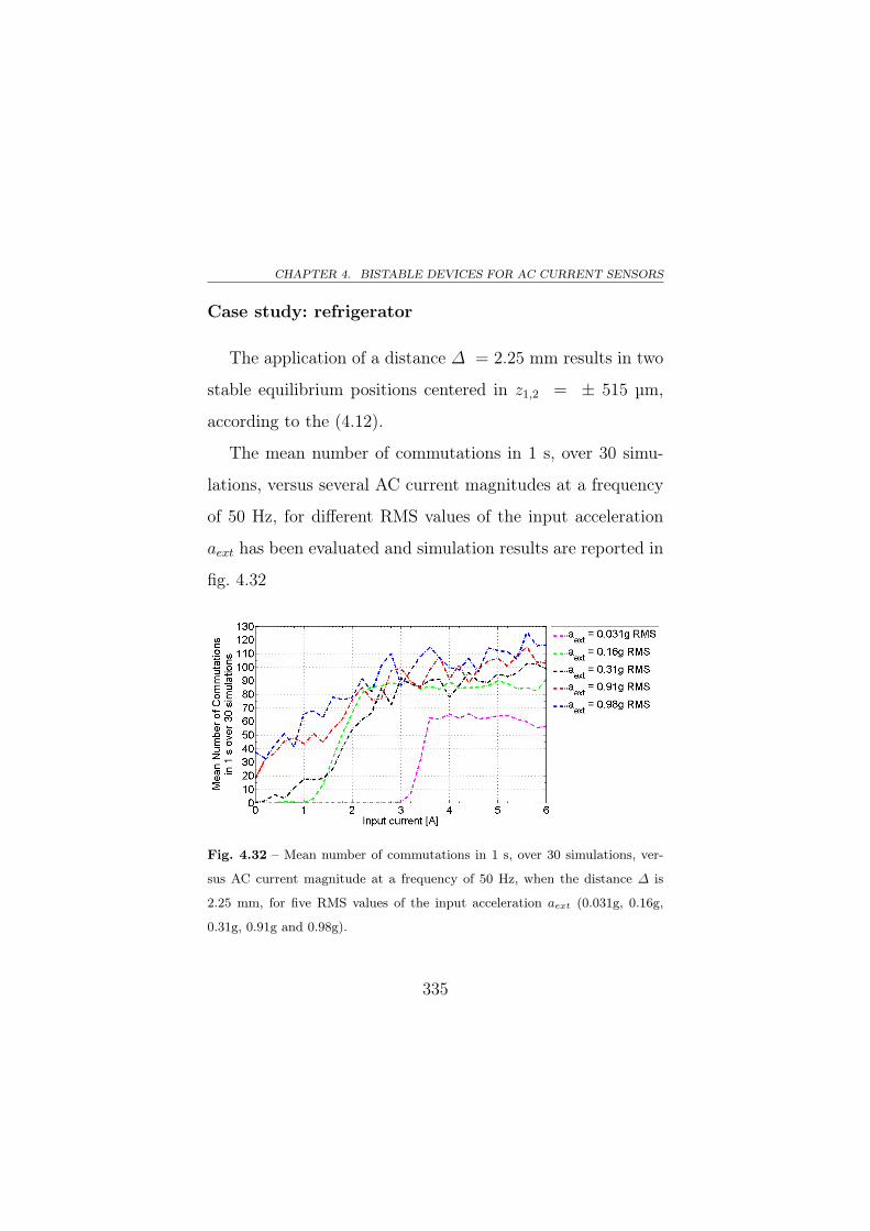
CHAPTER 4. BISTABLE DEVICES FOR AC CURRENT SENSORS
Case study: refrigerator
The application of a distance ∆ = 2.25 mm results in two
stable equilibrium positions centered in z1,2 = ± 515 µm,
according to the (4.12).
The mean number of commutations in 1 s, over 30 simu-
lations, versus several AC current magnitudes at a frequency
of 50 Hz, for different RMS values of the input acceleration
aext has been evaluated and simulation results are reported in
fig. 4.32
Fig. 4.32 – Mean number of commutations in 1 s, over 30 simulations, ver-
sus AC current magnitude at a frequency of 50 Hz, when the distance ∆ is
2.25 mm, for five RMS values of the input acceleration aext (0.031g, 0.16g,
0.31g, 0.91g and 0.98g).
335
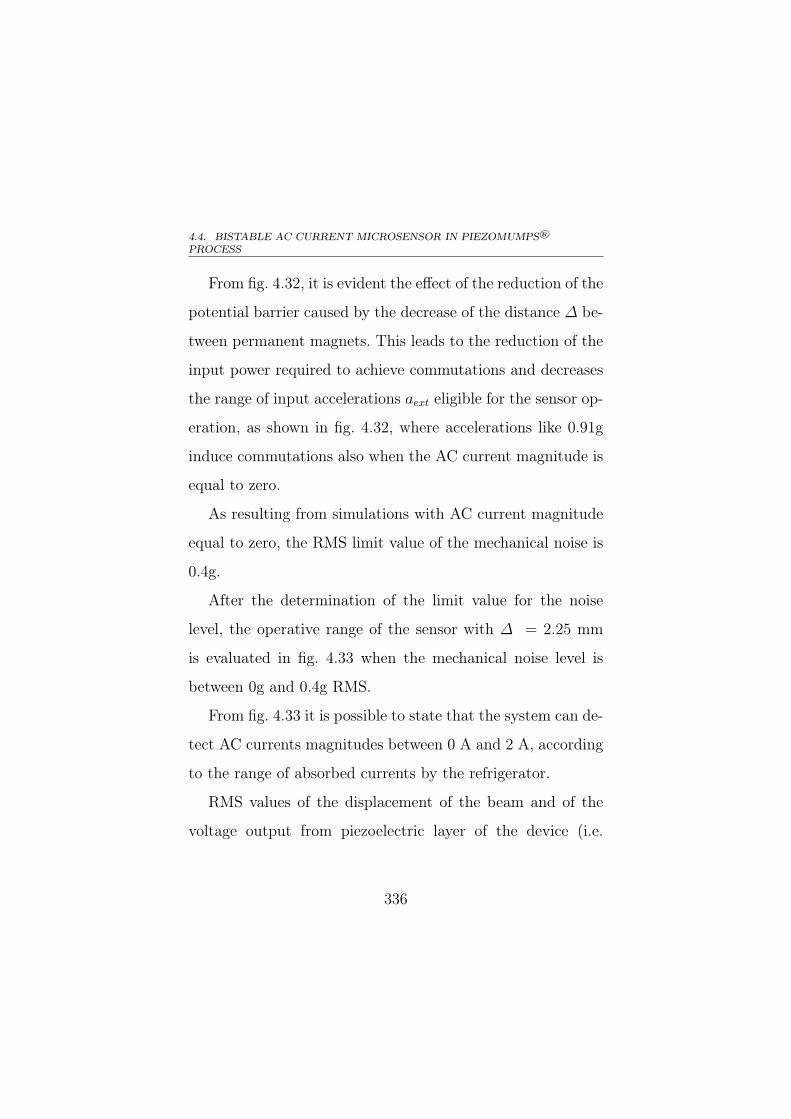
4.4. BISTABLE AC CURRENT MICROSENSOR IN PIEZOMUMPS®
PROCESS
From fig. 4.32, it is evident the effect of the reduction of the
potential barrier caused by the decrease of the distance ∆ be-
tween permanent magnets. This leads to the reduction of the
input power required to achieve commutations and decreases
the range of input accelerations aext eligible for the sensor op-
eration, as shown in fig. 4.32, where accelerations like 0.91g
induce commutations also when the AC current magnitude is
equal to zero.
As resulting from simulations with AC current magnitude
equal to zero, the RMS limit value of the mechanical noise is
0.4g.
After the determination of the limit value for the noise
level, the operative range of the sensor with ∆ = 2.25 mm
is evaluated in fig. 4.33 when the mechanical noise level is
between 0g and 0.4g RMS.
From fig. 4.33 it is possible to state that the system can de-
tect AC currents magnitudes between 0 A and 2 A, according
to the range of absorbed currents by the refrigerator.
RMS values of the displacement of the beam and of the
voltage output from piezoelectric layer of the device (i.e.
336
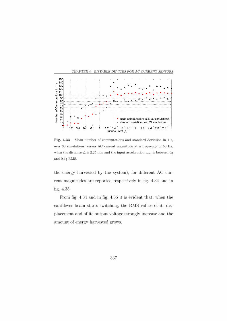
CHAPTER 4. BISTABLE DEVICES FOR AC CURRENT SENSORS
Fig. 4.33 – Mean number of commutations and standard deviation in 1 s,
over 30 simulations, versus AC current magnitude at a frequency of 50 Hz,
when the distance ∆ is 2.25 mm and the input acceleration aext is between 0g
and 0.4g RMS.
the energy harvested by the system), for different AC cur-
rent magnitudes are reported respectively in fig. 4.34 and in
fig. 4.35.
From fig. 4.34 and in fig. 4.35 it is evident that, when the
cantilever beam starts switching, the RMS values of its dis-
placement and of its output voltage strongly increase and the
amount of energy harvested grows.
337
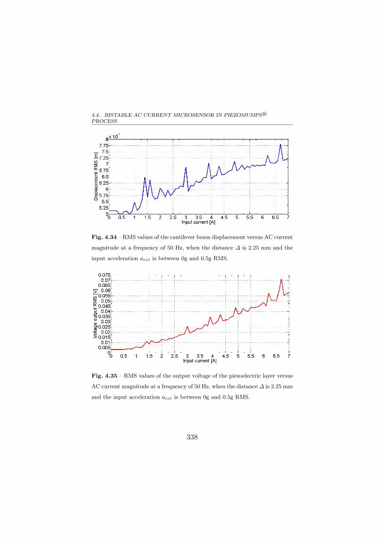
4.4. BISTABLE AC CURRENT MICROSENSOR IN PIEZOMUMPS®
PROCESS
Fig. 4.34 – RMS values of the cantilever beam displacement versus AC current
magnitude at a frequency of 50 Hz, when the distance ∆ is 2.25 mm and the
input acceleration aext is between 0g and 0.5g RMS.
Fig. 4.35 – RMS values of the output voltage of the piezoelectric layer versus
AC current magnitude at a frequency of 50 Hz, when the distance∆ is 2.25 mm
and the input acceleration aext is between 0g and 0.5g RMS.
338
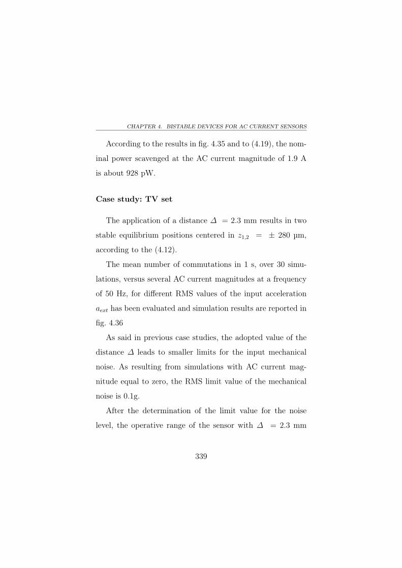
CHAPTER 4. BISTABLE DEVICES FOR AC CURRENT SENSORS
According to the results in fig. 4.35 and to (4.19), the nom-
inal power scavenged at the AC current magnitude of 1.9 A
is about 928 pW.
Case study: TV set
The application of a distance ∆ = 2.3 mm results in two
stable equilibrium positions centered in z1,2 = ± 280 µm,
according to the (4.12).
The mean number of commutations in 1 s, over 30 simu-
lations, versus several AC current magnitudes at a frequency
of 50 Hz, for different RMS values of the input acceleration
aext has been evaluated and simulation results are reported in
fig. 4.36
As said in previous case studies, the adopted value of the
distance ∆ leads to smaller limits for the input mechanical
noise. As resulting from simulations with AC current mag-
nitude equal to zero, the RMS limit value of the mechanical
noise is 0.1g.
After the determination of the limit value for the noise
level, the operative range of the sensor with ∆ = 2.3 mm
339

4.4. BISTABLE AC CURRENT MICROSENSOR IN PIEZOMUMPS®
PROCESS
Fig. 4.36 – Mean number of commutations in 1 s, over 30 simulations, versus
AC current magnitude at a frequency of 50 Hz, when the distance ∆ is 2.3 mm,
for five RMS values of the input acceleration aext (0.031g, 0.16g, 0.31g, 0.91g
and 0.98g).
is evaluated in fig. 4.37 when the mechanical noise level is
between 0g and 0.1g RMS.
From fig. 4.33 it is possible to state that the system can de-
tect AC current magnitudes between 0 A and 0.8 A, according
to the range of absorbed currents by the refrigerator.
RMS values of the displacement of the beam and of the
voltage output from the piezoelectric layer of the device (i.e.
the energy harvested by the system), for different AC cur-
340
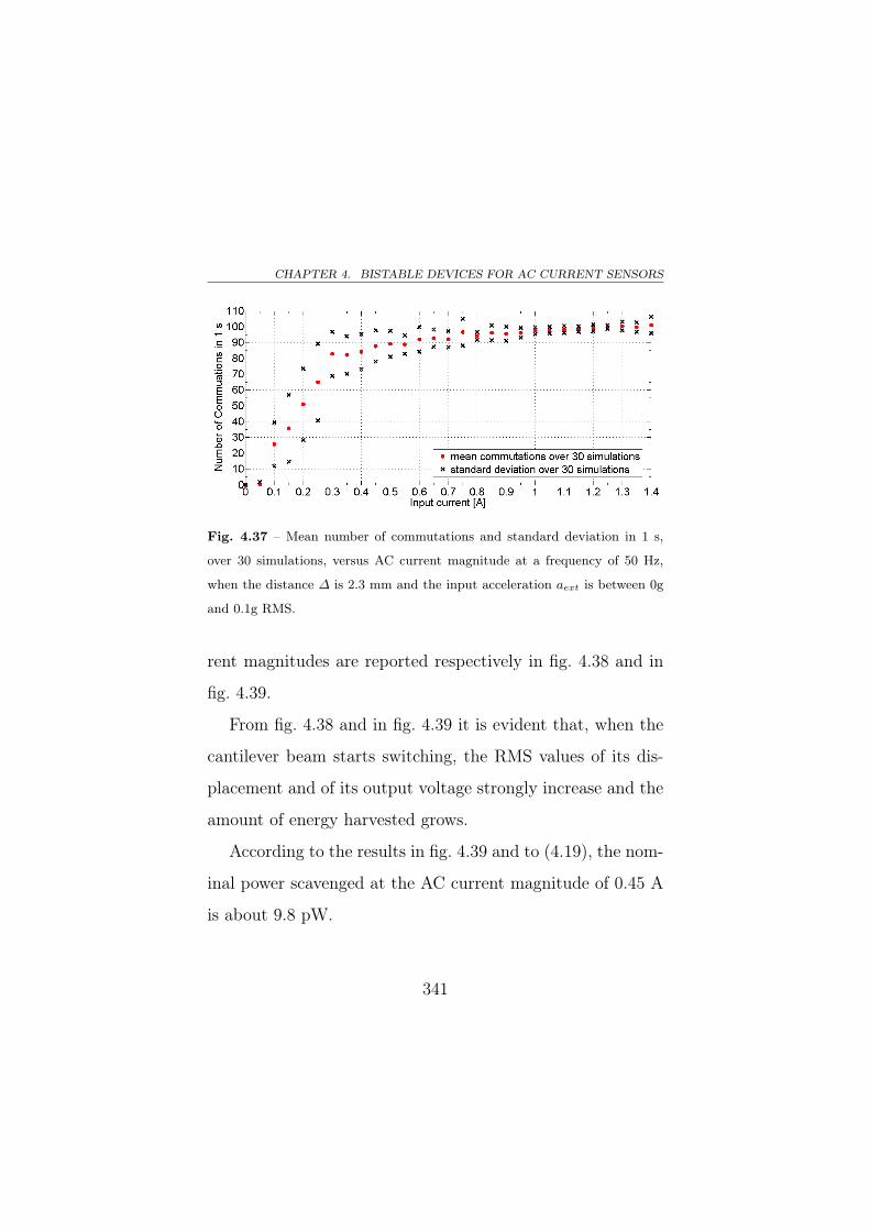
CHAPTER 4. BISTABLE DEVICES FOR AC CURRENT SENSORS
Fig. 4.37 – Mean number of commutations and standard deviation in 1 s,
over 30 simulations, versus AC current magnitude at a frequency of 50 Hz,
when the distance ∆ is 2.3 mm and the input acceleration aext is between 0g
and 0.1g RMS.
rent magnitudes are reported respectively in fig. 4.38 and in
fig. 4.39.
From fig. 4.38 and in fig. 4.39 it is evident that, when the
cantilever beam starts switching, the RMS values of its dis-
placement and of its output voltage strongly increase and the
amount of energy harvested grows.
According to the results in fig. 4.39 and to (4.19), the nom-
inal power scavenged at the AC current magnitude of 0.45 A
is about 9.8 pW.
341
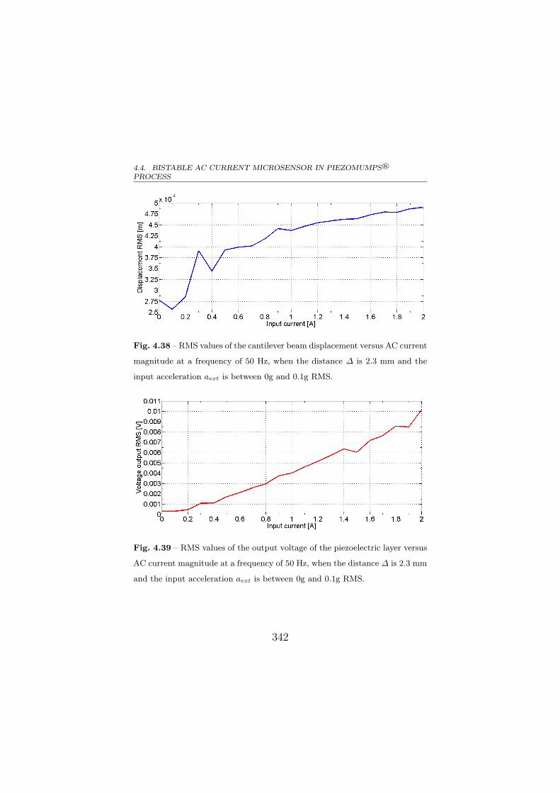
4.4. BISTABLE AC CURRENT MICROSENSOR IN PIEZOMUMPS®
PROCESS
Fig. 4.38 – RMS values of the cantilever beam displacement versus AC current
magnitude at a frequency of 50 Hz, when the distance ∆ is 2.3 mm and the
input acceleration aext is between 0g and 0.1g RMS.
Fig. 4.39 – RMS values of the output voltage of the piezoelectric layer versus
AC current magnitude at a frequency of 50 Hz, when the distance ∆ is 2.3 mm
and the input acceleration aext is between 0g and 0.1g RMS.
342
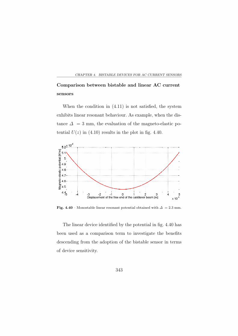
CHAPTER 4. BISTABLE DEVICES FOR AC CURRENT SENSORS
Comparison between bistable and linear AC current
sensors
When the condition in (4.11) is not satisfied, the system
exhibits linear resonant behaviour. As example, when the dis-
tance ∆ = 3 mm, the evaluation of the magneto-elastic po-
tential U(z) in (4.10) results in the plot in fig. 4.40.
Fig. 4.40 – Monostable linear resonant potential obtained with ∆ = 2.3 mm.
The linear device identified by the potential in fig. 4.40 has
been used as a comparison term to investigate the benefits
descending from the adoption of the bistable sensor in terms
of device sensitivity.
343
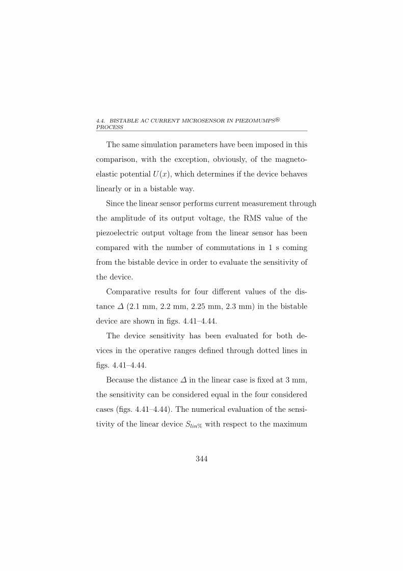
4.4. BISTABLE AC CURRENT MICROSENSOR IN PIEZOMUMPS®
PROCESS
The same simulation parameters have been imposed in this
comparison, with the exception, obviously, of the magneto-
elastic potential U(x), which determines if the device behaves
linearly or in a bistable way.
Since the linear sensor performs current measurement through
the amplitude of its output voltage, the RMS value of the
piezoelectric output voltage from the linear sensor has been
compared with the number of commutations in 1 s coming
from the bistable device in order to evaluate the sensitivity of
the device.
Comparative results for four different values of the dis-
tance ∆ (2.1 mm, 2.2 mm, 2.25 mm, 2.3 mm) in the bistable
device are shown in figs. 4.41–4.44.
The device sensitivity has been evaluated for both de-
vices in the operative ranges defined through dotted lines in
figs. 4.41–4.44.
Because the distance ∆ in the linear case is fixed at 3 mm,
the sensitivity can be considered equal in the four considered
cases (figs. 4.41–4.44). The numerical evaluation of the sensi-
tivity of the linear device Slin% with respect to the maximum
344
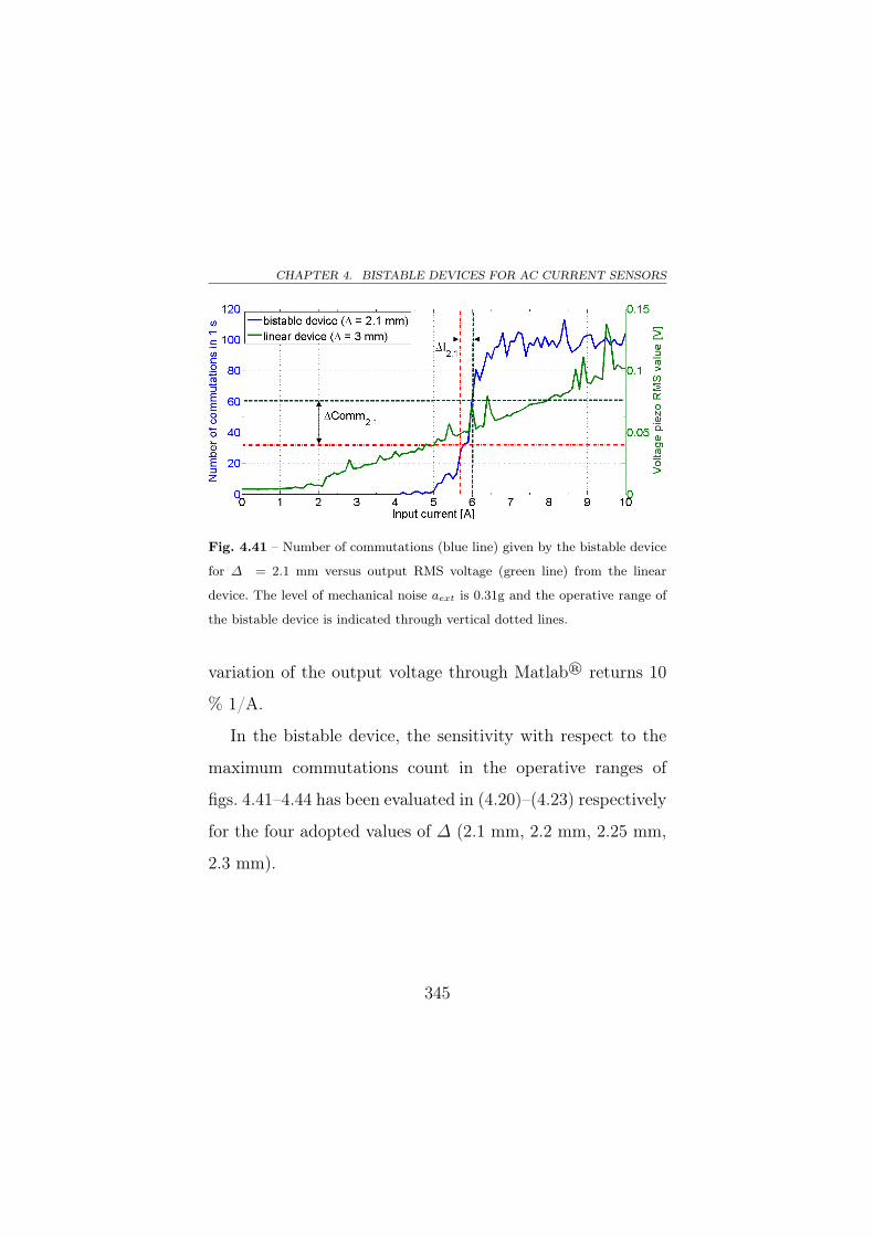
CHAPTER 4. BISTABLE DEVICES FOR AC CURRENT SENSORS
Fig. 4.41 – Number of commutations (blue line) given by the bistable device
for ∆ = 2.1 mm versus output RMS voltage (green line) from the linear
device. The level of mechanical noise aext is 0.31g and the operative range of
the bistable device is indicated through vertical dotted lines.
variation of the output voltage through Matlab® returns 10
% 1/A.
In the bistable device, the sensitivity with respect to the
maximum commutations count in the operative ranges of
figs. 4.41–4.44 has been evaluated in (4.20)–(4.23) respectively
for the four adopted values of ∆ (2.1 mm, 2.2 mm, 2.25 mm,
2.3 mm).
345
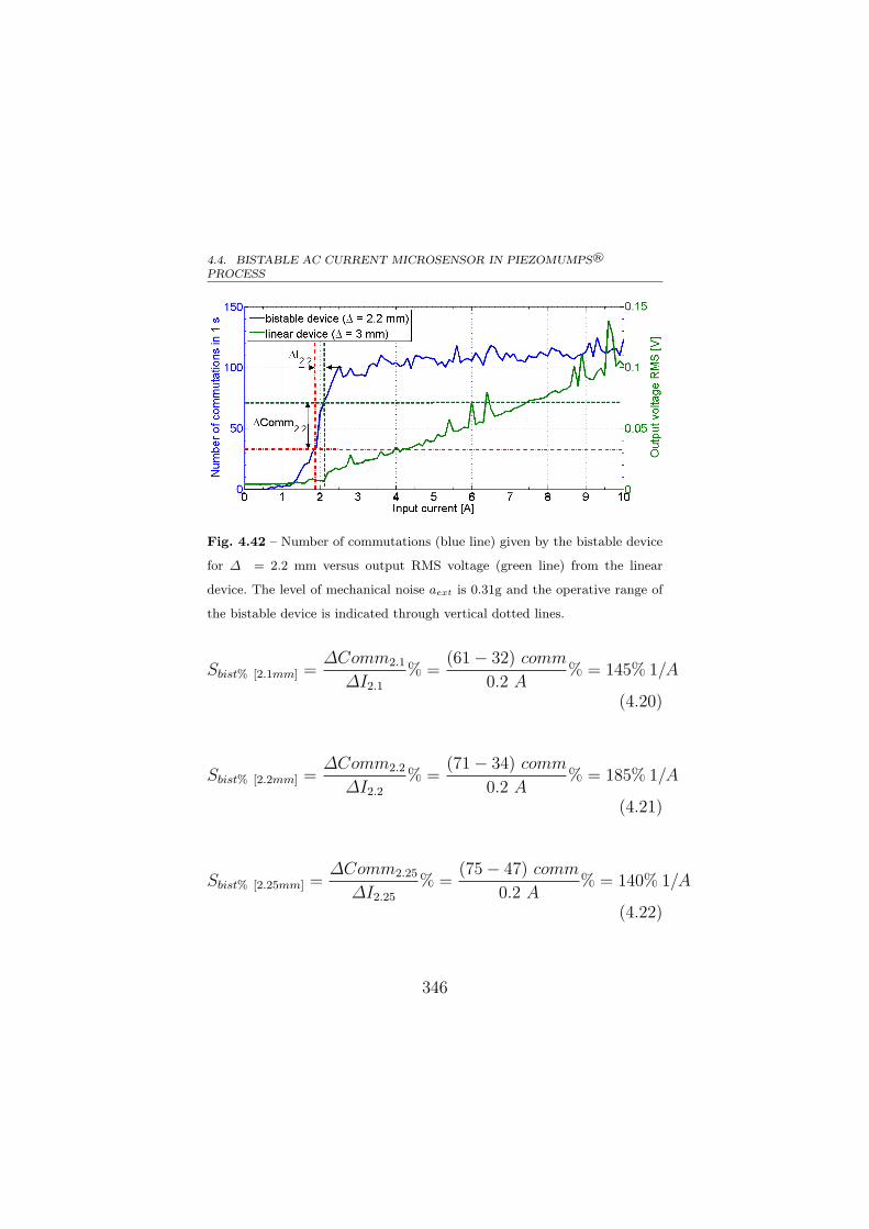
4.4. BISTABLE AC CURRENT MICROSENSOR IN PIEZOMUMPS®
PROCESS
Fig. 4.42 – Number of commutations (blue line) given by the bistable device
for ∆ = 2.2 mm versus output RMS voltage (green line) from the linear
device. The level of mechanical noise aext is 0.31g and the operative range of
the bistable device is indicated through vertical dotted lines.
Sbist% [2.1mm] =∆Comm2.1
∆I2.1% =
(61− 32) comm
0.2 A% = 145% 1/A
(4.20)
Sbist% [2.2mm] =∆Comm2.2
∆I2.2% =
(71− 34) comm
0.2 A% = 185% 1/A
(4.21)
Sbist% [2.25mm] =∆Comm2.25
∆I2.25% =
(75− 47) comm
0.2 A% = 140% 1/A
(4.22)
346
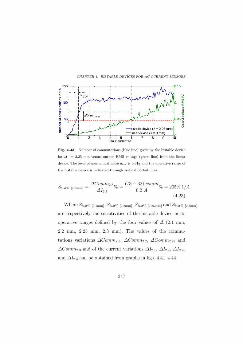
CHAPTER 4. BISTABLE DEVICES FOR AC CURRENT SENSORS
Fig. 4.43 – Number of commutations (blue line) given by the bistable device
for ∆ = 2.25 mm versus output RMS voltage (green line) from the linear
device. The level of mechanical noise aext is 0.31g and the operative range of
the bistable device is indicated through vertical dotted lines.
Sbist% [2.3mm] =∆Comm2.3
∆I2.3% =
(73− 32) comm
0.2 A% = 205% 1/A
(4.23)
Where Sbist% [2.1mm], Sbist% [2.2mm], Sbist% [2.25mm] and Sbist% [2.3mm]
are respectively the sensitivities of the bistable device in its
operative ranges defined by the four values of ∆ (2.1 mm,
2.2 mm, 2.25 mm, 2.3 mm). The values of the commu-
tations variations ∆Comm2.1, ∆Comm2.2, ∆Comm2.25 and
∆Comm2.3 and of the current variations ∆I2.1, ∆I2.2, ∆I2.25
and ∆I2.3 can be obtained from graphs in figs. 4.41–4.44.
347
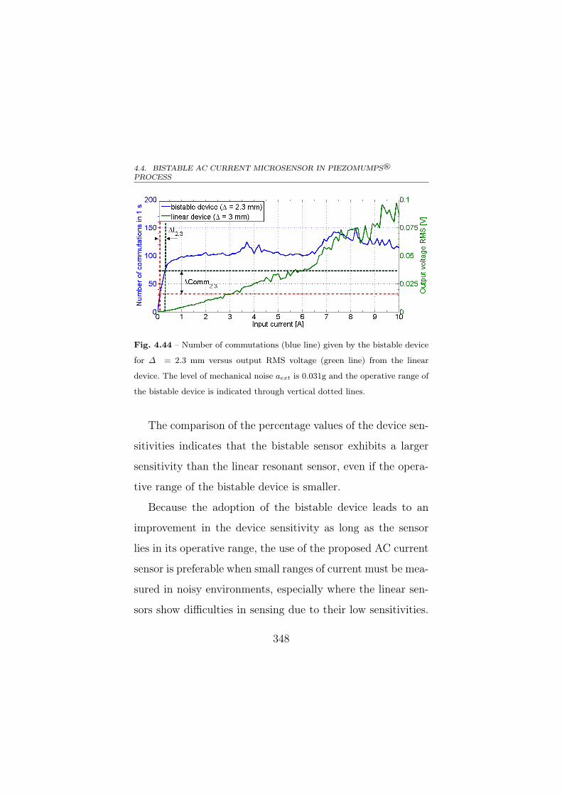
4.4. BISTABLE AC CURRENT MICROSENSOR IN PIEZOMUMPS®
PROCESS
Fig. 4.44 – Number of commutations (blue line) given by the bistable device
for ∆ = 2.3 mm versus output RMS voltage (green line) from the linear
device. The level of mechanical noise aext is 0.031g and the operative range of
the bistable device is indicated through vertical dotted lines.
The comparison of the percentage values of the device sen-
sitivities indicates that the bistable sensor exhibits a larger
sensitivity than the linear resonant sensor, even if the opera-
tive range of the bistable device is smaller.
Because the adoption of the bistable device leads to an
improvement in the device sensitivity as long as the sensor
lies in its operative range, the use of the proposed AC current
sensor is preferable when small ranges of current must be mea-
sured in noisy environments, especially where the linear sen-
sors show difficulties in sensing due to their low sensitivities.
348
CHAPTER 4. BISTABLE DEVICES FOR AC CURRENT SENSORS
The improvement in sensitivity offered by the nonlinearity in
the bistable device is more consistent when small amounts of
current have to be sensed, especially in applications requiring
the detection of the presence of a current flowing in a wire.
Finally, the possibility of tuning the magneto-elastic po-
tential of the bistable sensor through the distance ∆ between
permanent magnets can remedy the small operative range in
bistable sensor by adapting it to the application requirements.
Another advantage descending from the adoption of the bi-
stable device is related to its capability of scavenging a larger
amount of energy than the linear resonant device from its op-
erative environment. As resulting from the device simulations,
the power scavenged by the bistable device (for four different
values of ∆, 2.1 mm, 2.2 mm, 2.25 mm and 2.3 mm) has been
compared with that harvested by the linear resonant device
(∆ = 2.1 mm) in fig. 4.45 for several values of AC current
magnitude to be measured and a mechanical noise of 0.16g.
The values of power in fig. 4.45 have been computed through
the (4.19) and considering a resistive load RL of 330 kΩ.
349
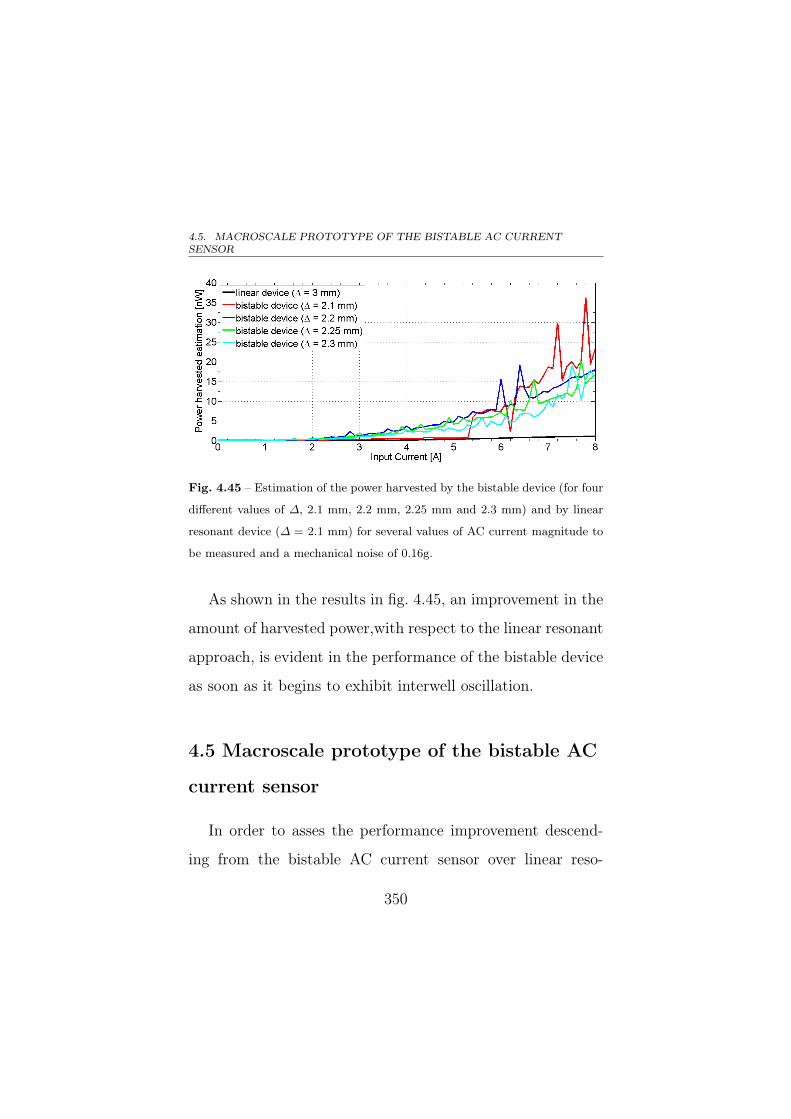
4.5. MACROSCALE PROTOTYPE OF THE BISTABLE AC CURRENTSENSOR
Fig. 4.45 – Estimation of the power harvested by the bistable device (for four
different values of ∆, 2.1 mm, 2.2 mm, 2.25 mm and 2.3 mm) and by linear
resonant device (∆ = 2.1 mm) for several values of AC current magnitude to
be measured and a mechanical noise of 0.16g.
As shown in the results in fig. 4.45, an improvement in the
amount of harvested power,with respect to the linear resonant
approach, is evident in the performance of the bistable device
as soon as it begins to exhibit interwell oscillation.
4.5 Macroscale prototype of the bistable AC
current sensor
In order to asses the performance improvement descend-
ing from the bistable AC current sensor over linear reso-
350
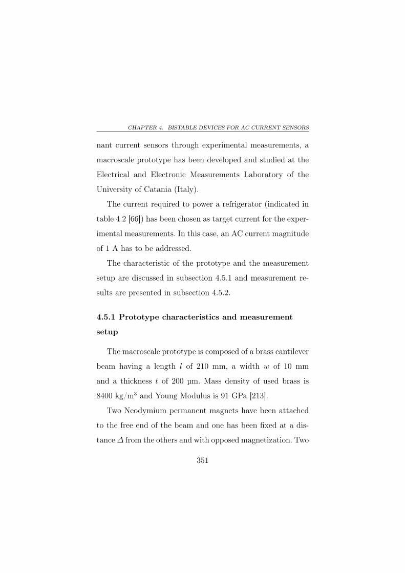
CHAPTER 4. BISTABLE DEVICES FOR AC CURRENT SENSORS
nant current sensors through experimental measurements, a
macroscale prototype has been developed and studied at the
Electrical and Electronic Measurements Laboratory of the
University of Catania (Italy).
The current required to power a refrigerator (indicated in
table 4.2 [66]) has been chosen as target current for the exper-
imental measurements. In this case, an AC current magnitude
of 1 A has to be addressed.
The characteristic of the prototype and the measurement
setup are discussed in subsection 4.5.1 and measurement re-
sults are presented in subsection 4.5.2.
4.5.1 Prototype characteristics and measurement
setup
The macroscale prototype is composed of a brass cantilever
beam having a length l of 210 mm, a width w of 10 mm
and a thickness t of 200 µm. Mass density of used brass is
8400 kg/m3 and Young Modulus is 91 GPa [213].
Two Neodymium permanent magnets have been attached
to the free end of the beam and one has been fixed at a dis-
tance∆ from the others and with opposed magnetization. Two
351
4.5. MACROSCALE PROTOTYPE OF THE BISTABLE AC CURRENTSENSOR
permanent magnets, instead of one, have been attached to the
tip of the cantilever beam in order to increase the overall vol-
ume Vm of the moving magnets and, consequently from (4.17),
to obtain a larger input magnetic force Fm(t), at the same in-
put current, acting on the beam. The necessity of a larger
input magnetic force Fm(t) is caused by the larger dimensions
of the beam and by the different material adopted.
Each of the used Neodymium magnets has a cylindrical
shape with a radius of 4 mm and a height of 4 mm. Values of
mass density and magnetic remanence Br for Neodymium are
listed in table 4.1. The piezoelectric mechanical-to-electrical
transduction is performed through a Lead Titanate Zirconate
(PZT) disk from Murata®, with integrated electrodes, at-
tached at the clamped end of the cantilever beam. The used
PZT disk has a radius of 4.5 mm and a height of 120 µm. A
load resistor RL of 330 kΩ has been connected to the output
electrodes of the PZT disk. Piezoelectric coupling in 31 di-
rection in stress-charge form e31 of PZT is -20.49 C/m2 and
electrical permittivity in 33 direction ε33 is 18.5 nF/m [213].
352
CHAPTER 4. BISTABLE DEVICES FOR AC CURRENT SENSORS
The output voltage on the load resistor RL is read through
an oscilloscope probe and acquired and visualized through a
digital oscilloscope.
The cable carrying the AC current to be measured has been
placed at a distance h of 1 mm from the moving magnets.
The AC current to be measured is obtained from the mains
voltage of 220 V, reduced through a transformer. The value of
the AC target current magnitude has been regulated through
a potentiometer connected to the output of the aforesaid
transformer and verified through an amperemeter.
It should be noted also that the presented prototype is
environmental friendly as it has been realized using recycled
materials.
A picture of the macroscale prototype of the cantilever
beam is reported in fig. 4.46; the transformer and the po-
tentiometer used for generation of the AC target current from
mains voltage are shown in fig. 4.47; a photo of the described
measurement setup is shown in fig. 4.48.
353
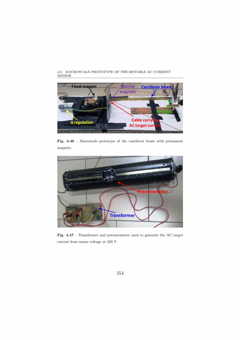
4.5. MACROSCALE PROTOTYPE OF THE BISTABLE AC CURRENTSENSOR
Fig. 4.46 – Macroscale prototype of the cantilever beam with permanent
magnets.
Fig. 4.47 – Transformer and potentiometer used to generate the AC target
current from mains voltage at 220 V.
354
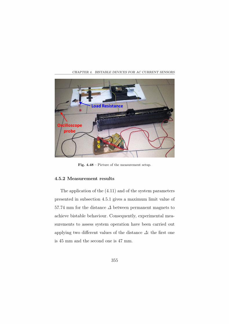
CHAPTER 4. BISTABLE DEVICES FOR AC CURRENT SENSORS
Fig. 4.48 – Picture of the measurement setup.
4.5.2 Measurement results
The application of the (4.11) and of the system parameters
presented in subsection 4.5.1 gives a maximum limit value of
57.74 mm for the distance ∆ between permanent magnets to
achieve bistable behaviour. Consequently, experimental mea-
surements to assess system operation have been carried out
applying two different values of the distance ∆: the first one
is 45 mm and the second one is 47 mm.
355
4.5. MACROSCALE PROTOTYPE OF THE BISTABLE AC CURRENTSENSOR
In order to compare performance of the bistable sensor
with a linear resonant version of the proposed device, a set of
measurements has been fulfilled employing a linear resonant
sensor realized through the elimination of the fixed magnet
from the measurement setup. Thus, a distance ∆ → +∞ is
imposed and linear resonant behaviour is achieved in this case.
No external mechanical noise aext has been applied in these
measurements.
Results of the measurement campaign are presented in the
following and a video of the measurement setup and of the
actuated beam is available on internet [218].
Measurement results for ∆ = 47 mm
According to (4.12), a distance ∆= 47 mm results in two
stable equilibrium positions z1,2 placed at± 30 mm from beam
fabrication position (z = 0 mm).
Considering the application of the refrigerator, an AC cur-
rent magnitude of 1 A has been imposed through the poten-
tiometer but no beam commutations have been observed as
confirmed by the acquired time series of the piezoelectric out-
put voltage reported in fig. 4.49.
356
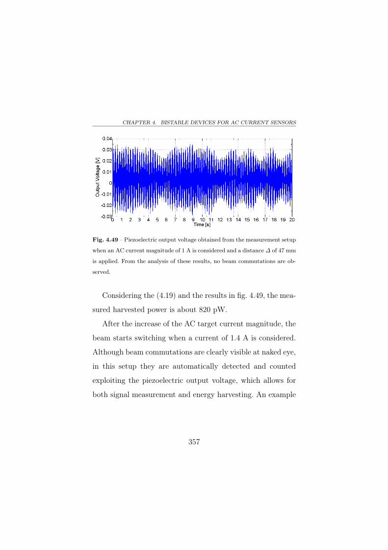
CHAPTER 4. BISTABLE DEVICES FOR AC CURRENT SENSORS
Fig. 4.49 – Piezoelectric output voltage obtained from the measurement setup
when an AC current magnitude of 1 A is considered and a distance ∆ of 47 mm
is applied. From the analysis of these results, no beam commutations are ob-
served.
Considering the (4.19) and the results in fig. 4.49, the mea-
sured harvested power is about 820 pW.
After the increase of the AC target current magnitude, the
beam starts switching when a current of 1.4 A is considered.
Although beam commutations are clearly visible at naked eye,
in this setup they are automatically detected and counted
exploiting the piezoelectric output voltage, which allows for
both signal measurement and energy harvesting. An example
357
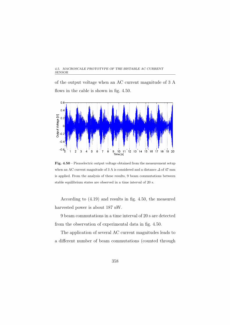
4.5. MACROSCALE PROTOTYPE OF THE BISTABLE AC CURRENTSENSOR
of the output voltage when an AC current magnitude of 3 A
flows in the cable is shown in fig. 4.50.
Fig. 4.50 – Piezoelectric output voltage obtained from the measurement setup
when an AC current magnitude of 3 A is considered and a distance ∆ of 47 mm
is applied. From the analysis of these results, 9 beam commutations between
stable equilibrium states are observed in a time interval of 20 s.
According to (4.19) and results in fig. 4.50, the measured
harvested power is about 187 nW.
9 beam commutations in a time interval of 20 s are detected
from the observation of experimental data in fig. 4.50.
The application of several AC current magnitudes leads to
a different number of beam commutations (counted through
358
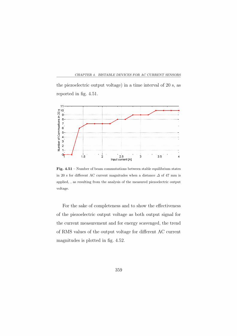
CHAPTER 4. BISTABLE DEVICES FOR AC CURRENT SENSORS
the piezoelectric output voltage) in a time interval of 20 s, as
reported in fig. 4.51.
Fig. 4.51 – Number of beam commutations between stable equilibrium states
in 20 s for different AC current magnitudes when a distance ∆ of 47 mm is
applied, , as resulting from the analysis of the measured piezoelectric output
voltage.
For the sake of completeness and to show the effectiveness
of the piezoelectric output voltage as both output signal for
the current measurement and for energy scavenged, the trend
of RMS values of the output voltage for different AC current
magnitudes is plotted in fig. 4.52.
359
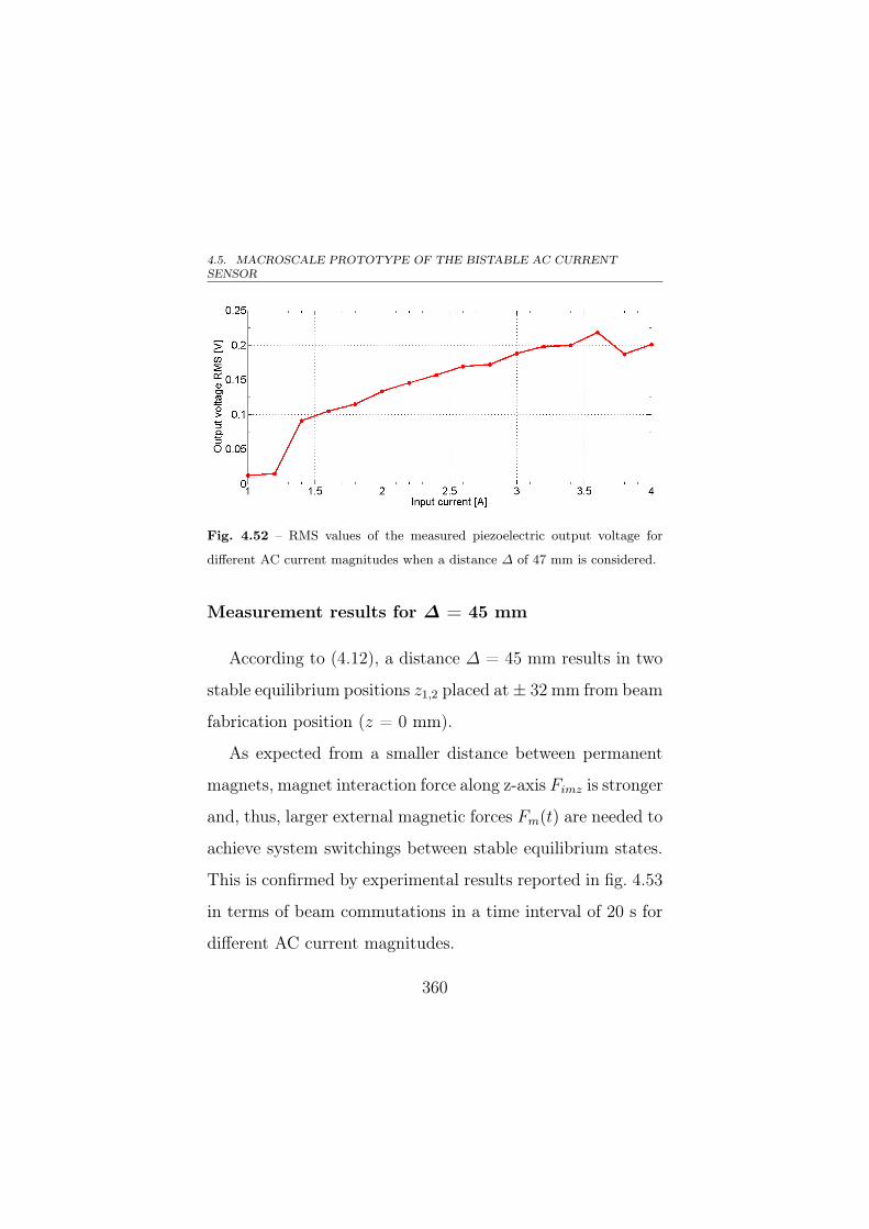
4.5. MACROSCALE PROTOTYPE OF THE BISTABLE AC CURRENTSENSOR
Fig. 4.52 – RMS values of the measured piezoelectric output voltage for
different AC current magnitudes when a distance ∆ of 47 mm is considered.
Measurement results for ∆ = 45 mm
According to (4.12), a distance ∆ = 45 mm results in two
stable equilibrium positions z1,2 placed at± 32 mm from beam
fabrication position (z = 0 mm).
As expected from a smaller distance between permanent
magnets, magnet interaction force along z-axis Fimz is stronger
and, thus, larger external magnetic forces Fm(t) are needed to
achieve system switchings between stable equilibrium states.
This is confirmed by experimental results reported in fig. 4.53
in terms of beam commutations in a time interval of 20 s for
different AC current magnitudes.
360
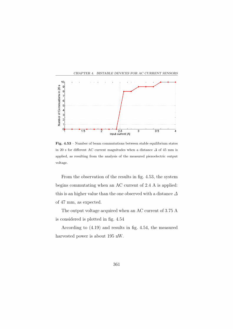
CHAPTER 4. BISTABLE DEVICES FOR AC CURRENT SENSORS
Fig. 4.53 – Number of beam commutations between stable equilibrium states
in 20 s for different AC current magnitudes when a distance ∆ of 45 mm is
applied, as resulting from the analysis of the measured piezoelectric output
voltage.
From the observation of the results in fig. 4.53, the system
begins commutating when an AC current of 2.4 A is applied:
this is an higher value than the one observed with a distance∆
of 47 mm, as expected.
The output voltage acquired when an AC current of 3.75 A
is considered is plotted in fig. 4.54
According to (4.19) and results in fig. 4.54, the measured
harvested power is about 195 nW.
361
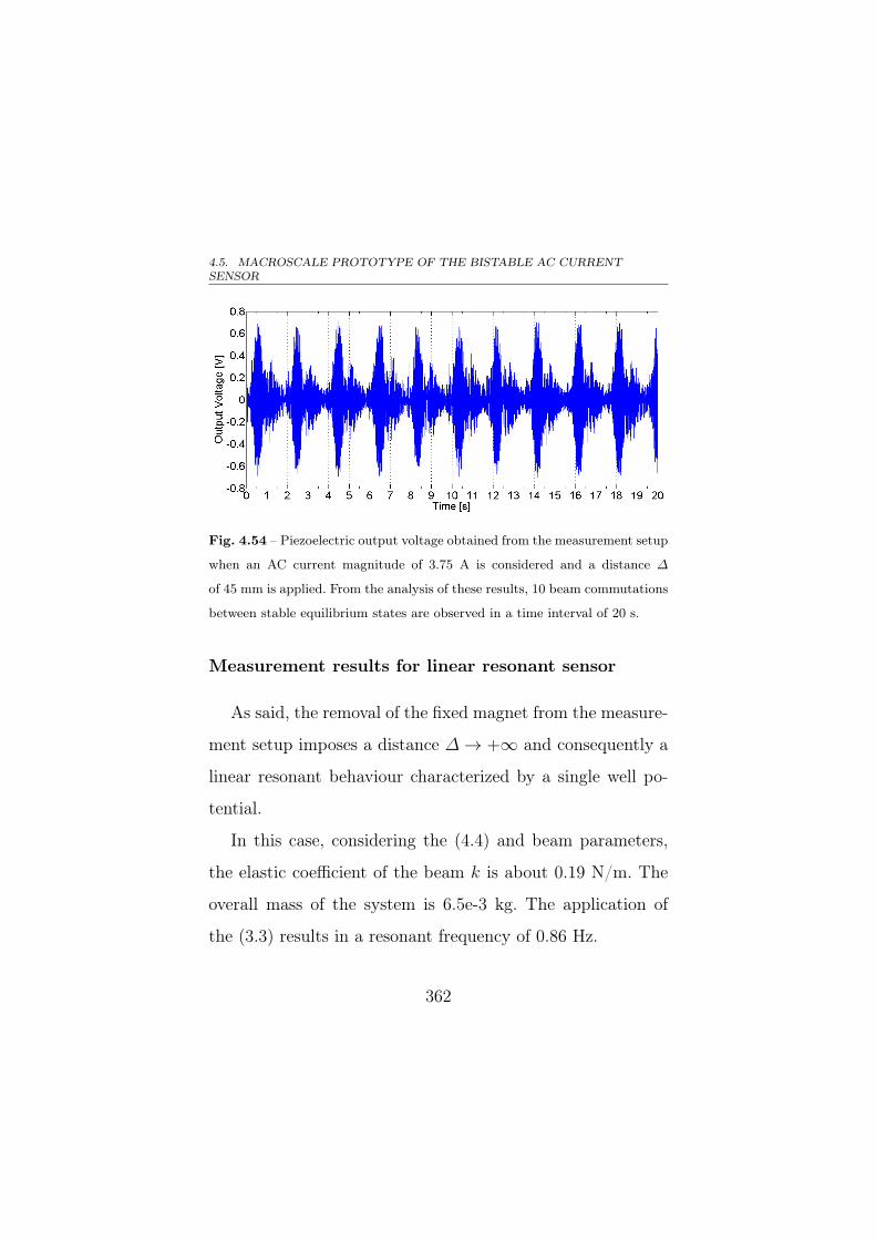
4.5. MACROSCALE PROTOTYPE OF THE BISTABLE AC CURRENTSENSOR
Fig. 4.54 – Piezoelectric output voltage obtained from the measurement setup
when an AC current magnitude of 3.75 A is considered and a distance ∆
of 45 mm is applied. From the analysis of these results, 10 beam commutations
between stable equilibrium states are observed in a time interval of 20 s.
Measurement results for linear resonant sensor
As said, the removal of the fixed magnet from the measure-
ment setup imposes a distance ∆→ +∞ and consequently a
linear resonant behaviour characterized by a single well po-
tential.
In this case, considering the (4.4) and beam parameters,
the elastic coefficient of the beam k is about 0.19 N/m. The
overall mass of the system is 6.5e-3 kg. The application of
the (3.3) results in a resonant frequency of 0.86 Hz.
362
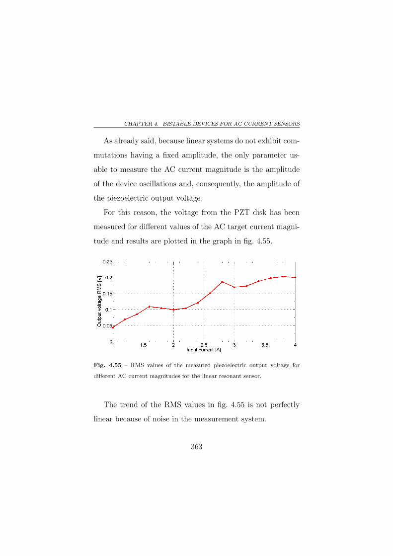
CHAPTER 4. BISTABLE DEVICES FOR AC CURRENT SENSORS
As already said, because linear systems do not exhibit com-
mutations having a fixed amplitude, the only parameter us-
able to measure the AC current magnitude is the amplitude
of the device oscillations and, consequently, the amplitude of
the piezoelectric output voltage.
For this reason, the voltage from the PZT disk has been
measured for different values of the AC target current magni-
tude and results are plotted in the graph in fig. 4.55.
Fig. 4.55 – RMS values of the measured piezoelectric output voltage for
different AC current magnitudes for the linear resonant sensor.
The trend of the RMS values in fig. 4.55 is not perfectly
linear because of noise in the measurement system.
363
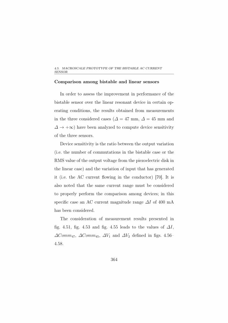
4.5. MACROSCALE PROTOTYPE OF THE BISTABLE AC CURRENTSENSOR
Comparison among bistable and linear sensors
In order to assess the improvement in performance of the
bistable sensor over the linear resonant device in certain op-
erating conditions, the results obtained from measurements
in the three considered cases (∆ = 47 mm, ∆ = 45 mm and
∆ → +∞) have been analyzed to compute device sensitivity
of the three sensors.
Device sensitivity is the ratio between the output variation
(i.e. the number of commutations in the bistable case or the
RMS value of the output voltage from the piezoelectric disk in
the linear case) and the variation of input that has generated
it (i.e. the AC current flowing in the conductor) [70]. It is
also noted that the same current range must be considered
to properly perform the comparison among devices; in this
specific case an AC current magnitude range ∆I of 400 mA
has been considered.
The consideration of measurement results presented in
fig. 4.51, fig. 4.53 and fig. 4.55 leads to the values of ∆I,
∆Comm47, ∆Comm45, ∆V1 and ∆V2 defined in figs. 4.56–
4.58.
364
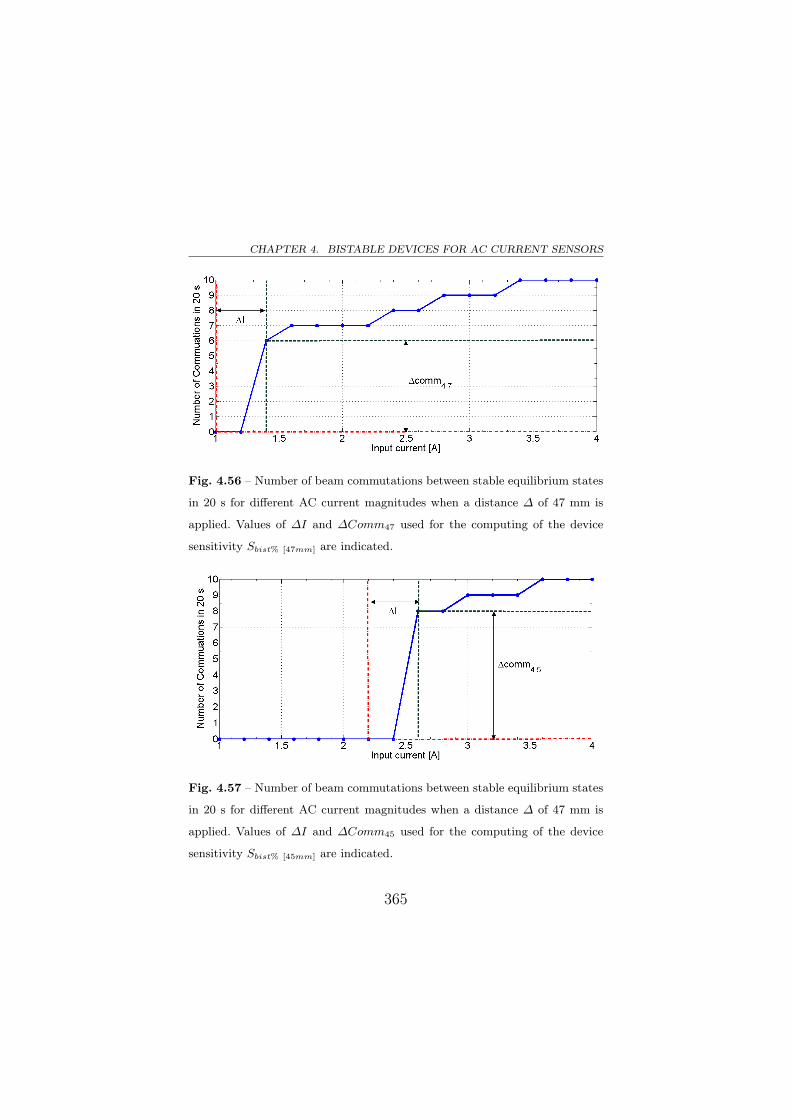
CHAPTER 4. BISTABLE DEVICES FOR AC CURRENT SENSORS
Fig. 4.56 – Number of beam commutations between stable equilibrium states
in 20 s for different AC current magnitudes when a distance ∆ of 47 mm is
applied. Values of ∆I and ∆Comm47 used for the computing of the device
sensitivity Sbist% [47mm] are indicated.
Fig. 4.57 – Number of beam commutations between stable equilibrium states
in 20 s for different AC current magnitudes when a distance ∆ of 47 mm is
applied. Values of ∆I and ∆Comm45 used for the computing of the device
sensitivity Sbist% [45mm] are indicated.
365
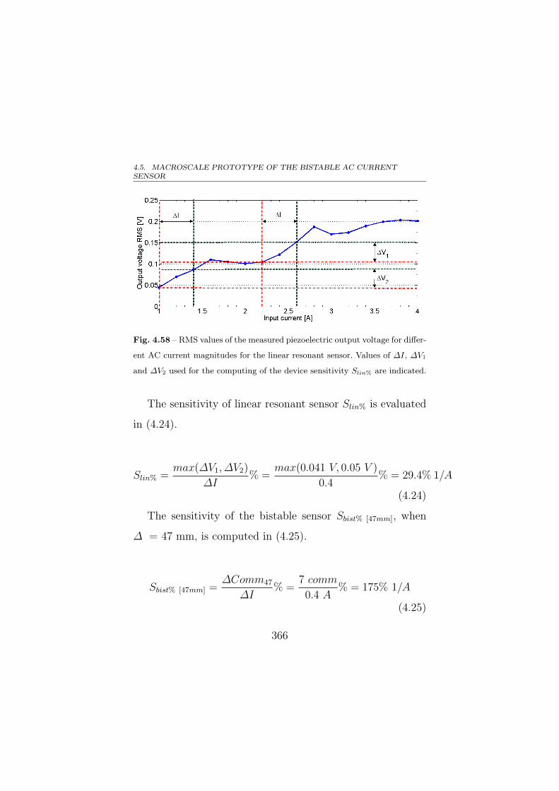
4.5. MACROSCALE PROTOTYPE OF THE BISTABLE AC CURRENTSENSOR
Fig. 4.58 – RMS values of the measured piezoelectric output voltage for differ-
ent AC current magnitudes for the linear resonant sensor. Values of ∆I, ∆V1
and ∆V2 used for the computing of the device sensitivity Slin% are indicated.
The sensitivity of linear resonant sensor Slin% is evaluated
in (4.24).
Slin% =max(∆V1, ∆V2)
∆I% =
max(0.041 V, 0.05 V )
0.4% = 29.4% 1/A
(4.24)
The sensitivity of the bistable sensor Sbist% [47mm], when
∆ = 47 mm, is computed in (4.25).
Sbist% [47mm] =∆Comm47
∆I% =
7 comm
0.4 A% = 175% 1/A
(4.25)
366
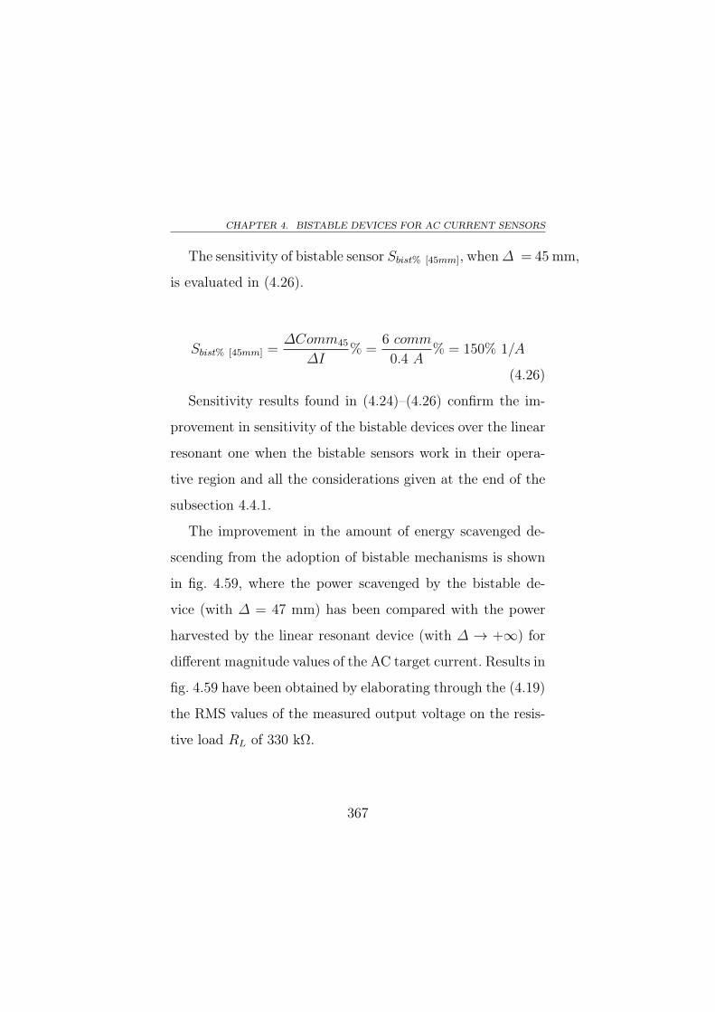
CHAPTER 4. BISTABLE DEVICES FOR AC CURRENT SENSORS
The sensitivity of bistable sensor Sbist% [45mm], when∆ = 45 mm,
is evaluated in (4.26).
Sbist% [45mm] =∆Comm45
∆I% =
6 comm
0.4 A% = 150% 1/A
(4.26)
Sensitivity results found in (4.24)–(4.26) confirm the im-
provement in sensitivity of the bistable devices over the linear
resonant one when the bistable sensors work in their opera-
tive region and all the considerations given at the end of the
subsection 4.4.1.
The improvement in the amount of energy scavenged de-
scending from the adoption of bistable mechanisms is shown
in fig. 4.59, where the power scavenged by the bistable de-
vice (with ∆ = 47 mm) has been compared with the power
harvested by the linear resonant device (with ∆ → +∞) for
different magnitude values of the AC target current. Results in
fig. 4.59 have been obtained by elaborating through the (4.19)
the RMS values of the measured output voltage on the resis-
tive load RL of 330 kΩ.
367
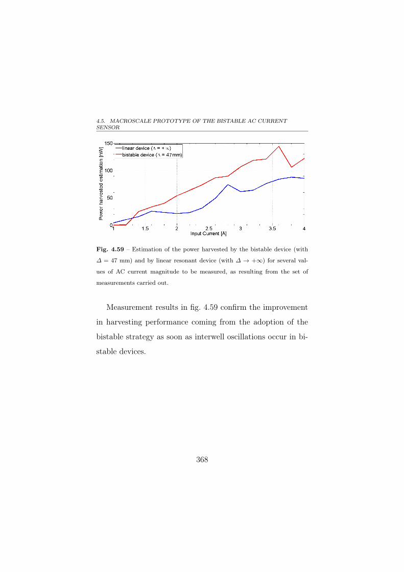
4.5. MACROSCALE PROTOTYPE OF THE BISTABLE AC CURRENTSENSOR
Fig. 4.59 – Estimation of the power harvested by the bistable device (with
∆ = 47 mm) and by linear resonant device (with ∆ → +∞) for several val-
ues of AC current magnitude to be measured, as resulting from the set of
measurements carried out.
Measurement results in fig. 4.59 confirm the improvement
in harvesting performance coming from the adoption of the
bistable strategy as soon as interwell oscillations occur in bi-
stable devices.
368
Conclusions
Imagine a mountain...From the top of this mountain, the view is wonderful.
You want to be there, but the summit seems so far away that you lose hope
of reaching it. You give up, saying “I will never get there”. The truth is, the
footsteps of the ones who reached the top were no bigger than yours. But they’d
just gone on putting those small footsteps one after the other. It’s not miracles
which make the impossible happen, it’s perseverance.
Serdar Özkan
The main aim of this work is focused on the study of the
beneficial effects of the adoption of nonlinear strategies, es-
pecially bistable mechanisms, in specific transducers applica-
tions.
Efforts have been paid in the identification and in the im-
plementation of technology solutions to fabricate/prototype

Conclusions
bistable devices at several scales. Both standard MEMS batch
processes and rapid prototyping strategies have been taken
into account. Among rapid prototyping solutions, processes
to release cantilever beams through Focused Ion Beam milling
and to deposit piezoelectric layers of Zinc Oxide have been de-
veloped at micro and nano-scale. At macro-scale (e.g., size of
a few centimeters), strategies based on low-cost inkjet print-
ing of electrically conductive inks on plastic flexible substrates
have adopted and investigated.
Two large application fields have been explored: one is rep-
resented by the energy harvesting from mechanical vibrations
and the other one by the sensing of AC currents through mi-
cromechanical structures.
In energy harvesting from mechanical vibrations, the appli-
cation of bistable devices based on fully compliant microstruc-
tures and buckled beams, respectively in MEMS standard pro-
cesses and direct printing technologies, has been investigated
through analytical models, FEM simulations and, where pro-
totypes have been fabricated, experimental tests. The widen-
ing of the bandwidth of harvesters has been demonstrated
370
Conclusions
with respect to traditional solutions adopting linear resonant
structures. As a consequence, a larger amount of harvested
energy has been proven with respect to linear strategies when
wideband vibrations at low frequency (e.g., below 500 Hz) are
taken as input.
In the field of the AC currents sensors, a novel nonlinear
transduction mechanism exploiting the number of beam com-
mutations between its stable equilibrium states to quantify
the magnitude of the target AC current has been proposed.
This approach leads to an improvement of the device sen-
sitivity in the device operative range over solutions adopting
linear resonant strategies. The self-generating operation of the
device, due to piezoelectric materials, allows also for the au-
tonomous operation of the device and to exploit ambient noise
to harvest energy along with its sensing operation.
371


Acknowledgements
And in the end the love you take is equal to the love you make.
The Beatles
This thesis concludes three years of work. During this very
important period of my life, I had the daily possibility to
grow and compare my knowledge and experiences with a great
group of researchers and friends. My personal and professional
growth and all the results reported in thesis are also due to
them.
First of all, I would like to thank Prof. Salvatore Baglio,
my tutor during these three years of Ph.D. course. For me,
he was a great mentor and an inexhaustible source of con-
stant inspiration, creativity, enthusiasm and motivation. All
Acknowledgements
my gratitude goes to him for believing in me and for guiding
me as a father every day in this important life path.
I would like to thank Prof. Luigi Fortuna, the coordinator
of my Ph.D. course, for his constant support and motivation.
I owe a big thank to Prof. Bruno Andò who steadily
gave me support and many valuable suggestions which indeed
helped me in my personal growth and in improving my expe-
rience during these years. His precious help in the research on
devices in direct printing technology is part of the results of
this work.
I would like to thank Prof. Salvatore Graziani for his sug-
gestions and the important tutorship experience in his course
about “Electric and Electronic Measurements”.
Special thanks go to all the guys of the “Measurement
Group” and “Automation and Control of Complex Systems,
Robotic Group” of the University of Catania (Italy) for daily
sharing this beautiful experience and for several mutual in-
formation exchanges that have been very relevant to improve
my knowledge: we lived together a really great adventure. In
particular, among them, I want to thank Carlo Trigona, An-
374
Acknowledgements
gela Beninato, Elena Umana, Vincenzo Marletta, Salvatore
La Malfa, Felice Maiorca, Fabio Antoci, Fabio Giusa, Ilenia
Medico, Stefania Medico, Valentina Sinatra, Giuseppe Vitel-
laro, Antonio Pistorio and Viviana De Luca. I wish you all
the best in your lives.
A big thank goes to the people from the company “Ad-
vanced Technology Solutions” of Catania (Alfonso D’Agostino,
Francesca Cunsolo, Valentina La Paglia and Dr. Ada Di Ste-
fano) for their “logistical” and “friendly” support in my activ-
ities at the Nanotechlab of Catania (Italy).
I have to thank Prof. Graziella Malandrino and Prof. Guido
Condorelli from Department of Chemistry of the University
of Catania (Italy) for the X-Ray Diffraction and Energy Dis-
persive X-Ray Spectroscopy analyses of the ZnO samples.
A big thank is for Prof. Lucia Romano from the Depart-
ment of Physics of the University of Catania (Italy) for the
Rutherford Backscattering Spectroscopy analyses of the ZnO
samples and for her precious suggestions when I started work-
ing with the Scanning Electron Microscope and the Focused
Ion Beam of the Nanotechlab of Catania (Italy).
375

Acknowledgements
Last but non least, I want to thank my family: my father
Alfio, my mother Giuseppa and my brother Giuseppe for their
love, their support and for always believing in me in all my
life choices. Also my relatives and my friends deserve thanks:
they were always on my side during these years. All that I am
I owe to them and to those that are no more with us.
Thank you very much.
376
A
Activities during Ph.D. course
A.1 Publications on international journals
• B. Andò, S. Baglio, G. L’Episcopo, V. Marletta, N. Savalli
and C. Trigona. “A BE-SOI MEMS for inertial measure-
ment in geophysical applications”. IEEE Transactions on
Instrumentation and Measurement, vol. 60, no. 5 , pp. 1991–
1908, 2011.
• B. Andò, S. Baglio, G. L’Episcopo and C. Trigona. “In-
vestigation on Mechanically Bi-stable MEMS Devices for
Energy Harvesting from Vibrations”. IEEE Journal of Mi-
croelectromechanical Systems, vol. 21, I. 4, pp. 779–790,
2012.
A.2. INTERNATIONAL CONFERENCE PROCEEDINGS
• B. Andò, S. Baglio and G. L’Episcopo. “A low cost, dispos-
able and contactless resonant mass sensor”. IEEE Trans-
actions on Instrumentation and Measurement, vol. 62, I. 1,
pp. 246–252, 2012.
• G. Vitellaro, G. L’Episcopo, C. Trigona, B. Andò and S.
Baglio. “A Compliant MEMS device for Out-of-Plane Dis-
placements with Thermo-Electric Actuation”. In press on
IEEE Journal of Microelectromechanical System.
A.2 International conference proceedings
• B. Andò, S. Baglio and G. L’Episcopo. “Lateral cantilever
beam in BESOI technology”. IEEE Instrumentation and
Measurement Technology Conference (I2MTC), 2011, Bin-
jang (China), pp. 1–6.
• B. Andò, S. Baglio, S. La Malfa and G. L’Episcopo. “All
inkjet printed system for strain measurement”. IEEE Sen-
sors 2011, Limerick (Ireland), pp. 215–217, 2011.
• S. Baglio, C. Trigona, B. Andò, F. Maiorca, G. L’Episcopo
and A. Beninato. “Energy Harvesting from weak random
vibrations: Bistable strategies and architectures for MEMS
378
APPENDIX A. ACTIVITIES DURING PH.D. COURSE
devices”. IEEE 55th International Midwest Symposium on
Circuits and Systems (MWSCAS), pp. 154–157, 2012.
• B. Andò, S. Baglio, M. Baù A.R. Bulsara, V. Ferrari, M.
Ferrari and G. L’Episcopo. “Nonlinear Energy Harvester by
Direct Printing Technology”. Procedia Engineering, vol. 47,
pp. 933–936 (2012). Eurosensors XXVI, Kraków (Poland),
2012
• B. Andò, S. Baglio, G. L’Episcopo, F. Maiorca and C. Trig-
ona. “Autonomous bistable microsensors for noninvasive
AC electrical current measurements”. IEEE Instrumenta-
tion and Measurement Technology Conference (I2MTC),
2013, Minneapolis (USA), pp. 93–97.
A.3 Book contributions
• B. Andò, S. Baglio, A. Beninato, G. L’Episcopo and G.
Trigona. “A Review on RTD-Fluxgate Magnetometers: From
Single to Coupled Core and Toward Novel Systems with
Innovative Materials” in “Sensors”, pp. 283-286, Springer,
2013.
379
A.5. ITALIAN CONFERENCE PROCEEDINGS
• B. Andò, S. Baglio, G. L’Episcopo and G. Trigona. “Mi-
crosensors for Harsh Environments: Review on Strategies
for Contactless and Self-Powered Systems” in “Sensors”,
pp. 219-222, Springer, 2013.
• B. Andò, S. Baglio and G. L’Episcopo. “Low cost inkjet
printed sensors” in “Sensors”, pp. 31-36, Springer, 2013.
A.4 Publications on Italian journals
• B. Andò, S. Baglio, G. L’Episcopo, C. Lombardo, V. Mar-
letta, I. Medico and S. Medico. “Prototipazione rapida di
sensori: tecnologie, materiali e applicazioni”. Tutto Misure,
year. XIV, no. 3 , pp. 177–182, 2012.
A.5 Italian conference proceedings
• B. Andò, S. Baglio, S. Graziani, G. L’Episcopo and N.
Pitrone. “Sviluppo di dispositivi MEMS bistabili per vibra-
tion energy harvesting a elevata efficienza”. GMEE 2010,
Gaeta (Italy).
380
APPENDIX A. ACTIVITIES DURING PH.D. COURSE
• B. Andò, S. Baglio, A. Beninato and G. L’Episcopo. “Strate-
gie di sviluppo e fabbricazione di nanosensori”. GMEE
2011, Genova (Italy).
• B. Andò, S. Baglio, N. Dumas, L. Latorre, G. L’Episcopo,
P. Nouet and C. Trigona. “Study and experimental valida-
tion of periodically-forced non-resonant oscillators for en-
ergy harvesting from vibrations”. Convegno Nazionale Sen-
sori 2012, Roma (Italy).
• B. Andò, S. Baglio and G. L’Episcopo. “Low cost Inkjet
printed sensors”. Convegno Nazionale Sensori 2012, Roma
(Italy).
• B. Andò, S. Baglio, S. Graziani and G. L’Episcopo. “Sviluppo
di dispositivi MEMS meccanicamente bistabili per energy
harvesting da vibrazioni meccaniche”. GMEE 2012, Monop-
oli (Italy).
• B. Andò, S. Baglio, A. Beninato, S. Graziani and G. L’Episcopo.
“Strategie di sviluppo e prototipazione rapida di nanosen-
sori”. GMEE 2012, Monopoli (Italy).
• B. Andò, S. Baglio, S. Graziani, G. L’Episcopo, F. Maiorca
and C. Trigona. “Un sensore autonomo e bistable per la
381
A.8. ATTENDED CONTESTS
misura non invasiva di correnti elettriche alternate”. GMEE
2013, Trento (Italy).
A.6 Attended conferences
• Convegno Nazionale Sensori. 15th–17th February 2012. Rome
(Italy).
• Eurosensors XXVI. 9th–12th September 2012. Kraków (Poland).
A.7 Attended Ph.D. schools
• Scuola di dottorato in Ingegneria dei Sistemi 2011. 12th
September 2011 – 7th October 2011. University of Catania
(Italy).
• International Student Conference on Microtechnology. 8th–
14th October 2012. Freiburg im Breisgau (Germany).
A.8 Attended contests
• “Science Presentation Competition” at the International
Student Conference on Microtechnology. 8th–14th October
2012. Freiburg im Breisgau (Germany).
382

APPENDIX A. ACTIVITIES DURING PH.D. COURSE
A.9 Attended courses at the University of
Catania (Italy)
• Sistemi elettrici per energia.
• Fisica tecnica.
• Impianti Elettrici I.
A.10 Tutoring Activities at University of
Catania (Italy)
• Misure elettriche ed elettroniche (2011).
383

References
General References
[22] S. Baglio, S. Castorina, and N. Savalli. Scaling issues
and design of MEMS. Wiley Online Library, 2007 (cit.
on p. 219).
[24] Minhang Bao and Heng Yang. “Squeeze film air damp-
ing in MEMS”. In: Sensors and Actuators A: Physical
136.1 (2007), pp. 3–27 (cit. on p. 134).
[36] Ronald Newbold Bracewell and RN Bracewell. The
Fourier transform and its applications. Vol. 31999.
McGraw-Hill New York, 1986 (cit. on p. 149).
[38] Bernard Brogliato. “Absolute stability and the Lagrange–
Dirichlet theorem with monotone multivalued map-
References
pings”. In: Systems & control letters 51.5 (2004), pp. 343–
353 (cit. on p. 14).
[44] John Charles Butcher. The numerical analysis of or-
dinary differential equations: Runge-Kutta and gen-
eral linear methods. Wiley-Interscience, 1987 (cit. on
p. 311).
[53] Y.H. Cho, A.P. Pisano, and R.T. Howe. “Viscous damp-
ing model for laterally oscillating microstructures”. In:
Journal of Microelectromechanical Systems 3.2 (1994),
pp. 81–87 (cit. on p. 220).
[70] Ernest O Doebelin. Measuring Systems - Application
and Design. McGraw-Hill, New York, 1990 (cit. on
pp. 7, 364).
[73] Georg Duffing. Erzwungene Schwingungen bei verän-
derlicher Eigenfrequenz und ihre technische Bedeutung.
R, Vieweg & Sohn, 1918 (cit. on pp. 23, 24, 145).
[84] Gene F Franklin, J David Powell, and Abbas Emami-
Naeini. Feedback control of dynamic systems. Vol. 320.
Addison-Wesley Reading, MA, 1991 (cit. on p. 7).
386
References
[93] Gustav Gautschi. Piezoelectric sensorics: force, strain,
pressure, acceleration and acoustic emission sensors,
materials and amplifiers. Springer, 2002 (cit. on pp. 158,
159).
[110] Xiao-Ting He, Shan-Lin Chen, and Jun-Yi Sun. “Ap-
plying the equivalent section method to solve beam
subjected to lateral force and bending-compression col-
umn with different moduli”. In: International Journal
of Mechanical Sciences 49.7 (2007), pp. 919–924 (cit.
on p. 296).
[115] MA Howaston, GP Lund, and DJ Todd. Engineer-
ing tables and data. Chapman and hall, 1991 (cit. on
p. 246).
[116] Larry L Howell. Compliant mechanisms. Wiley-Interscience,
2001 (cit. on pp. 13, 15, 17, 23, 46, 190, 199).
[129] P.E. Kloeden and E. Platen. Numerical solution of
stochastic differential equations. Springer, 1995 (cit. on
pp. 200, 201).
387
References
[131] Jan Korvink and Oliver Paul.MEMS: A practical guide
to design, analysis and applications. William Andrew,
2005 (cit. on pp. 43, 169, 283).
[139] R. Lensink, H. Bo, and E. Sterken. Investment, capital
market imperfections, and uncertainty: theory and em-
pirical results. Edward Elgar Pub, 2001 (cit. on p. 201).
[148] Aleksandr Mikhailovich Lyapunov. “The general prob-
lem of the stability of motion”. In: International Jour-
nal of Control 55.3 (1992), pp. 531–534 (cit. on p. 12).
[163] Ned Mohan, Tore M Undeland, and William P Rob-
bins. Power electronics: Converters, applications, and
design. Wiley (New York), 1989 (cit. on pp. 157, 284).
[175] Henry W Ott. Electromagnetic compatibility engineer-
ing. Wiley. com, 2011 (cit. on p. 323).
[177] Ramon Pallas-Areny, John GWebster, and Ramo Areny.
Sensors and signal conditioning. Wiley New York, 2001
(cit. on p. 8).
[194] Singiresu Rao. Mechanical Vibrations. Pearson Pren-
tice Hall, 2004 (cit. on pp. 121, 123).
388
References
[199] Raymond Jefferson Roark and Warren Clarence Young.
Formulas for stress and strain. McGraw-Hill, 1975 (cit.
on pp. 251, 296).
[210] Otto H Schmitt. “A thermionic trigger”. In: Journal of
Scientific Instruments 15.1 (1938), p. 24 (cit. on p. 23).
[212] Raymond A Serway, Chris Vuille, and Jerry S Faughn.
College physics. Vol. 10. Cengage Learning, 2008 (cit.
on pp. 15, 16, 145, 168, 182, 260, 280, 295, 299, 300,
321, 329).
[213] James F Shackelford and William Alexander. CRC ma-
terials science and engineering handbook. CRC press,
2010 (cit. on pp. 193, 246, 307, 351, 352).
[219] Gabriel G Skitek, Stanley V Marshall, and Richard
E DuBroff. Electromagnetic concepts and applications.
Prentice-Hall, 1982 (cit. on p. 279).
[227] Steven Strogatz. Nonlinear dynamics and chaos: with
applications to physics, biology, chemistry and engi-
neering. Perseus Books Group, 2001 (cit. on p. 8).
[241] Timo Veijola and Marek Turowski. “Compact damping
models for laterally moving microstructures with gas-
389

References
rarefaction effects”. In: Journal of Microelectromechan-
ical Systems 10.2 (2001), pp. 263–273 (cit. on p. 134).
[242] Benedetto Vigna. “Future of MEMS: an industry point
of view”. In: EuroSime 2006. 7th International Confer-
ence on Thermal, Mechanical and Multiphysics Simula-
tion and Experiments in Micro-Electronics and Micro-
Systems, 2006. IEEE. 2006, pp. 1–8 (cit. on pp. 44, 62,
63, 169).
[243] Daniel D Villani. “An analytic solution for the force
between two magnetic dipoles”. In: Magnetic and Elec-
trical Separation 9 (1998), pp. 39–52 (cit. on p. 296).
[249] John-G Webster. The Measurement, Instrumentation,
and Sensors: Handbook. Springer, 1999 (cit. on pp. 6,
277).
[250] Birron Mathew Weedy, Brian John Cory, N Jenkins,
JB Ekanayake, and G Strbac. Electric power systems.
John Wiley & Sons, 2012 (cit. on p. 276).
[266] QQ Zhang, SJ Gross, S Tadigadapa, TN Jackson, FT
Djuth, and S Trolier-McKinstry. “Lead zirconate ti-
tanate films for d33 mode cantilever actuators”. In: Sen-
390
References
sors and Actuators A: Physical 105.1 (2003), pp. 91–97
(cit. on p. 163).
Nonlinearity and Stochastic Resonance
[2] L Alfonsi, L Gammaitoni, S Santucci, and AR Bul-
sara. “Intrawell stochastic resonance versus interwell
stochastic resonance in underdamped bistable systems”.
In: Physical Review E 62.1 (2000), p. 299 (cit. on p. 10).
[12] Bruno Andò, Salvatore Baglio, Adi Bulsara, Vincenzo
Marletta, and Nicolo Savalli. “E-field ferroelectric sen-
sors: Modeling and simulation [Instrumentation Notes]”.
In: Instrumentation & Measurement Magazine, IEEE
12.2 (2009), pp. 31–37 (cit. on pp. 11, 64, 65).
[13] Bruno Andò, Salvatore Baglio, Adi R Bulsara, and
Vincenzo Marletta. “A Ferroelectric-Capacitor-Based
Approach to Quasistatic Electric Field Sensing”. In:
IEEE Transactions on Instrumentation and Measure-
ment 59.3 (2010), pp. 641–652 (cit. on pp. 11, 32, 65).
[14] Bruno Andò, Salvatore Baglio, Adi R Bulsara, and Vin-
cenzo Sacco. “Residence times difference fluxgate”. In:
391
References
Measurement 38.2 (2005), pp. 89–112 (cit. on pp. 11,
32).
[25] Roland Bartussek, Peter Hänggi, and Peter Jung. “Stochas-
tic resonance in optical bistable systems”. In: Physical
Review E 49.5 (1994), p. 3930 (cit. on p. 29).
[29] Roberto Benzi, Giorgio Parisi, Alfonso Sutera, and An-
gelo Vulpiani. “A theory of stochastic resonance in cli-
matic change”. In: SIAM Journal on applied mathemat-
ics 43.3 (1983), pp. 565–578 (cit. on p. 10).
[34] Wolfgang Bornhöfft and Gerhard Trenkler. “Magnetic
field sensors: Flux gate sensors”. In: Sensors Set: A
Comprehensive Survey (1989), pp. 153–203 (cit. on
p. 29).
[40] Adi R Bulsara and Luca Gammaitoni. “Tuning in to
noise”. In: Physics Today 49 (1996), p. 39 (cit. on pp. 9,
21–23, 25, 26, 28, 30, 291).
[41] Adi R Bulsara, Visarath In, Andy Kho, Antonio Pala-
cios, Patrick Longhini, Joe Neff, Gregory Anderson,
Christopher Obra, Salvatore Baglio, and Bruno Andò.
“Exploiting nonlinear dynamics in a coupled-core flux-
392
References
gate magnetometer”. In:Measurement Science and Tech-
nology 19.7 (2008), p. 075203 (cit. on p. 11).
[42] Adi R Bulsara, C Seberino, L Gammaitoni, MF Karls-
son, B Lundqvist, and JWC Robinson. “Signal detec-
tion via residence-time asymmetry in noisy bistable de-
vices”. In: Physical Review E 67.1 (2003), p. 016120
(cit. on p. 11).
[43] AR Bulsara, ME Inchiosa, and L Gammaitoni. “Noise-
controlled resonance behavior in nonlinear dynamical
systems with broken symmetry”. In: Physical review
letters 77.11 (1996), p. 2162 (cit. on p. 24).
[67] A Dari, L Bosi, and L Gammaitoni. “Nonlinear sensors:
An approach to the residence time detection strategy”.
In: Physical Review E 81.1 (2010), p. 011115 (cit. on
p. 10).
[76] FJ Elmer. “Bistability and strange nonlinear neutral
curve in ferromagnetic resonance”. In: Physics Letters
A 118.1 (1986), pp. 25–28 (cit. on p. 146).
[77] FJ Elmer. “Nonlinear and nonlocal dynamics of spa-
tially extended systems: stationary states, bifurcations
393
References
and stability”. In: Physica D: Nonlinear Phenomena
30.3 (1988), pp. 321–342 (cit. on pp. 148, 149).
[88] L Gammaitoni and AR Bulsara. “Noise activated non-
linear dynamic sensors”. In: Physical review letters 88.23
(2002), p. 230601 (cit. on pp. 10, 23, 30, 32, 37, 290,
319).
[89] L Gammaitoni, P Hänggi, P Jung, and F March-
esoni. “Stochastic Resonance: A remarkable idea that
changed our perception of noise”. In: The European
Physical Journal B 69.1 (2009), pp. 1–3 (cit. on p. 10).
[90] L Gammaitoni, F Marchesoni, E Menichella-Saetta, S
Santucci, et al. “Stochastic resonance in bistable sys-
tems”. In: Physical review letters 62.4 (1989), pp. 349–
352 (cit. on p. 12).
[91] Luca Gammaitoni, Peter Hänggi, Peter Jung, and Fabio
Marchesoni. “Stochastic resonance”. In: Reviews of mod-
ern physics 70.1 (1998), p. 223 (cit. on p. 9).
[92] Luca Gammaitoni, Igor Neri, and Helios Vocca. “The
benefits of noise and nonlinearity: Extracting energy
394
References
from random vibrations”. In: Chemical Physics 375.2
(2010), pp. 435–438 (cit. on pp. 8, 11, 290).
[101] John Guckenheimer and Philip Holmes. Nonlinear os-
cillations, dynamical systems, and bifurcations of vec-
tor fields. Springer-Verlag, 1983 (cit. on p. 146).
[104] Peter Hänggi, Mario E Inchiosa, Dave Fogliatti, and
Adi R Bulsara. “Nonlinear stochastic resonance: The
saga of anomalous output-input gain”. In: Physical Re-
view E 62.5 (2000), p. 6155 (cit. on p. 10).
[105] Peter Hänggi and Fabio Marchesoni. “Artificial Brow-
nian motors: Controlling transport on the nanoscale”.
In: Reviews of Modern Physics 81.1 (2009), p. 387 (cit.
on p. 9).
[106] Gregory Peter Harmer, Bruce R Davis, and Derek Ab-
bott. “A review of stochastic resonance: Circuits and
measurement”. In: Instrumentation and Measurement,
IEEE Transactions on 51.2 (2002), pp. 299–309 (cit. on
p. 26).
[113] PJ Holmes and DA Rand. “The bifurcations of Duff-
ing’s equation: An application of catastrophe theory”.
395
References
In: Journal of Sound and Vibration 44.2 (1976), pp. 237–
253 (cit. on pp. 146, 147).
[114] John J Hopfield. “Neurons with graded response have
collective computational properties like those of two-
state neurons”. In: Proceedings of the national academy
of sciences 81.10 (1984), pp. 3088–3092 (cit. on p. 24).
[128] Seunghwan Kim, Seon Hee Park, and H-B Pyo. “Stochas-
tic resonance in coupled oscillator systems with time
delay”. In: Physical review letters 82.8 (1999), p. 1620
(cit. on p. 28).
[164] Faisal Mohd-Yasin, N Zaiyadi, DJ Nagel, DS Ong, CE
Korman, and AR Faidz. “Noise and reliability measure-
ment of a three-axis micro-accelerometer”. In: Micro-
electronic Engineering 86.4 (2009), pp. 991–995 (cit.
on p. 169).
[167] Alexander Neiman and Lutz Schimansky-Geier. “Stochas-
tic resonance in bistable systems driven by harmonic
noise”. In: Physical review letters 72.19 (1994), p. 2988
(cit. on p. 12).
396
References
[171] A Nikitin, NG Stocks, and AR Bulsara. “Asymmet-
ric bistable systems subject to periodic and stochas-
tic forcing in the strongly nonlinear regime: Switching
time distributions”. In: Physical Review E 68.1 (2003),
p. 016103 (cit. on p. 14).
[226] NG Stocks, ND Stein, and Peter VEMcClintock. “Stochas-
tic resonance in monostable systems”. In: Journal of
Physics A: Mathematical and General 26.7 (1993),
p. L385 (cit. on p. 28).
[228] Torsten Strunz and Franz-Josef Elmer. “Driven Frenkel-
Kontorova model in uniform sliding states and dynam-
ical domains of different particle densities”. In: Physical
Review E 58.2 (1998), p. 1601 (cit. on p. 150).
Bistable Systems
[35] P Boyle, DF Moore, R Breen, RRA Syms, H Zou, and
J Stagg. “MEMS bistable clamp with electrical lock-
ing and release”. In: 15th Micromechanics Workshop,
MME’04. 2004, pp. 45–48 (cit. on p. 186).
397
References
[39] M Brokate and AV Pokrovskiı. “Asymptotically sta-
ble oscillations in systems with hysteresis nonlineari-
ties”. In: Journal of differential equations 150.1 (1998),
pp. 98–123 (cit. on p. 23).
[46] Jasmina Casals-Terre, Andreu Fargas-Marques, and
Andrei M Shkel. “Snap-action bistable micromecha-
nisms actuated by nonlinear resonance”. In: Journal of
Microelectromechanical Systems 17.5 (2008), pp. 1082–
1093 (cit. on p. 18).
[50] Mu Chiao and Liwei Lin. “Self-buckling of microma-
chined beams under resistive heating”. In: Journal of
Microelectromechanical Systems 9.1 (2000), pp. 146–
151 (cit. on p. 255).
[65] Luke J Currano, Miao Yu, and Balakumar Balachan-
dran. “Latching in a MEMS shock sensor: Modeling
and experiments”. In: Sensors and Actuators A: Phys-
ical 159.1 (2010), pp. 41–50 (cit. on p. 33).
[98] Troy Gomm, Larry L Howell, and Richard H Selfridge.
“In-plane linear displacement bistable microrelay”. In:
398
References
Journal of Micromechanics and Microengineering 12.3
(2002), p. 257 (cit. on p. 19).
[103] Beat Hälg. “On a micro-electro-mechanical nonvolatile
memory cell”. In: IEEE Transactions on Electron De-
vices 37.10 (1990), pp. 2230–2236 (cit. on p. 255).
[117] Il-Han Hwang, Yu-Seok Shim, and Jong-Hyun Lee.
“Modeling and experimental characterization of the
chevron-type bi-stable microactuator”. In: Journal of
Micromechanics and Microengineering 13.6 (2003), p. 948
(cit. on p. 19).
[132] W Kreider and Ali H Nayfeh. “Experimental investiga-
tion of single-mode responses in a fixed-fixed buckled
beam”. In: Nonlinear Dynamics 15.2 (1998), pp. 155–
177 (cit. on p. 18).
[147] Rajesh Luharuka and Peter J Hesketh. “Design of fully
compliant, in-plane rotary, bistable micromechanisms
for MEMS applications”. In: Sensors and Actuators A:
Physical 134.1 (2007), pp. 231–238 (cit. on p. 19).
[154] Tadao Matsunaga and Masayoshi Esashi. “Acceleration
switch with extended holding time using squeeze film
399
References
effect for side airbag systems”. In: Sensors and Actua-
tors A: physical 100.1 (2002), pp. 10–17 (cit. on p. 33).
[165] P Mormile, L Petti, M Abbate, P Musto, G Ragosta,
and P Villano. “Temperature switch and thermally in-
duced optical bistability in a PDLC”. In: Optics com-
munications 147.4-6 (1998), pp. 269–273 (cit. on p. 34).
[169] NT Nguyen. “Micromachined flow sensors - a review”.
In: Flow measurement and Instrumentation 8.1 (1997),
pp. 7–16 (cit. on p. 34).
[170] Son D Nguyen, Einar Halvorsen, and Igor Paprotny.
“Bistable springs for wideband microelectromechanical
energy harvesters”. In: Applied Physics Letters 102.2
(2013), pp. 023904–023904 (cit. on pp. 39, 155).
[173] Patrick G Opdahl, Brian D Jensen, and Larry L How-
ell. “An investigation into compliant bistable mecha-
nisms”. In: Proc. 1998 ASME Design Engineering Tech-
nical Conf. 1998, pp. 13–16 (cit. on p. 15).
[179] M.B. Parkinson, B.D. Jensen, and G.M. Roach. “Optimization-
based design of a fully-compliant bistable micromech-
anism”. In: Proceedings of the 2000 ASME Design En-
400
References
gineering Technical Conferences, DETC2000/MECH-
14119 (2000) (cit. on p. 186).
[191] Jin Qiu, Jeffrey H Lang, and Alexander H Slocum. “A
centrally-clamped parallel-beam bistable MEMS mech-
anism”. In: Micro Electro Mechanical Systems, 2001.
MEMS 2001. The 14th IEEE International Conference
on. IEEE. 2001, pp. 353–356 (cit. on p. 46).
[192] Jin Qiu, Jeffrey H Lang, and Alexander H Slocum. “A
curved-beam bistable mechanism”. In: Journal of Mi-
croelectromechanical Systems 13.2 (2004), pp. 137–146
(cit. on p. 255).
[195] Gabriel M Rebeiz and Jeremy B Muldavin. “RF MEMS
switches and switch circuits”. In: Microwave Magazine,
IEEE 2.4 (2001), pp. 59–71 (cit. on p. 19).
[207] M Taher A Saif. “On a tunable bistable MEMS - theory
and experiment”. In: Journal of Microelectromechanical
Systems 9.2 (2000), pp. 157–170 (cit. on p. 255).
[211] Arjun Selvakumar, Navid Yazdi, and Khalil Najafi. “A
wide-range micromachined threshold accelerometer ar-
ray and interface circuit”. In: Journal of Micromechan-
401
References
ics and Microengineering 11.2 (2001), p. 118 (cit. on
p. 33).
[220] U Sonmez. “Compliant MEMS crash sensor designs: the
preliminary simulation results”. In: Intelligent Vehicles
Symposium, 2007 IEEE. IEEE. 2007, pp. 303–308 (cit.
on p. 19).
[236] Jinni Tsay, Liang-Qing Su, and Cheng-Kuo Sung. “De-
sign of a linear micro-feeding system featuring bistable
mechanisms”. In: Journal of Micromechanics and Mi-
croengineering 15.1 (2005), p. 63 (cit. on pp. 19, 186).
[239] Mattias Vangbo and Ylva Bäcklund. “A lateral sym-
metrically bistable buckled beam”. In: Journal of Mi-
cromechanics and Microengineering 8.1 (1998), p. 29
(cit. on p. 255).
[240] M Vázquez, C Gómez-Polo, D-X Chen, and A Her-
nando. “Magnetic bistability of amorphous wires and
sensor applications”. In: IEEE Transactions on Mag-
netics 30.2 (1994), pp. 907–912 (cit. on p. 34).
402
References
[254] Thomas Wilhelm. “The smallest chemical reaction sys-
tem with bistability”. In: BMC systems biology 3.1
(2009), p. 90 (cit. on p. 23).
[267] Jian Zhao, Yintang Yang, Kefeng Fan, Ping Hu, and
Hongxi Wang. “A bistable threshold accelerometer with
fully compliant clamped-clamped mechanism”. In: Sen-
sors Journal, IEEE 10.5 (2010), pp. 1019–1024 (cit. on
p. 33).
Technology References
[5] B Andò, S Baglio, M Baù, V Ferrari, E Sardini, N
Savalli, M Serpelloni, and C Trigona. “Contactless elec-
tromagnetic interrogation of a MEMS-based microres-
onator used as passive sensing element”. In: Solid-
State Sensors, Actuators and Microsystems Confer-
ence, 2009. TRANSDUCERS 2009. International. IEEE.
2009, pp. 1429–1432 (cit. on p. 50).
[10] Bruno Andò, S Baglio, G L’Episcopo, and C Trig-
ona. “Microsensors for Harsh Environments: Review on
403
References
Strategies for Contactless and Self-Powered Systems”.
In: Sensors. Springer, 2014, pp. 219–222 (cit. on p. 50).
[11] Brunò Ando and Salvatore Baglio. “Inkjet-printed sen-
sors: A useful approach for low cost, rapid prototyping
[Instrumentation Notes]”. In: Instrumentation & Mea-
surement Magazine, IEEE 14.5 (2011), pp. 36–40 (cit.
on p. 100).
[15] Bruno Andò, Salvatore Baglio, Salvatore La Malfa, and
Gaetano L’Episcopo. “All inkjet printed system for
strain measurement”. In: IEEE Sensors, 2011. IEEE.
2011, pp. 215–217 (cit. on pp. 105, 109).
[16] Bruno Andò, Salvatore Baglio, Gaetano L’Episcopo,
Vincenzo Marletta, Nicolò Savalli, and Carlo Trigona.
“A BE-SOI MEMS for inertial measurement in geo-
physical applications”. In: Instrumentation and Mea-
surement, IEEE Transactions on 60.5 (2011), pp. 1901–
1908 (cit. on p. 50).
[18] Bruno Andò, Salvatore Baglio, Nicolo Savalli, and Carlo
Trigona. “Cascaded “Triple-Bent-Beam” MEMS Sensor
for Contactless Temperature Measurements in Nonac-
404
References
cessible Environments”. In: IEEE Transactions on In-
strumentation and Measurement 60.4 (2011), pp. 1348–
1357 (cit. on pp. 52, 243).
[21] S Baglio, B Ando, and G L’Episcopo. “Lateral can-
tilever beam in BESOI technology”. In: Instrumenta-
tion and Measurement Technology Conference (I2MTC),
2011 IEEE. IEEE. 2011, pp. 1–6 (cit. on p. 50).
[31] Mark T Bohr. “Nanotechnology goals and challenges
for electronic applications”. In: IEEE Transactions on
Nanotechnology 1.1 (2002), pp. 56–62 (cit. on p. 69).
[37] Martin Brischwein, Sigrun Herrmann, Winfried Vonau,
Frank Berthold, Helmut Grothe, Elena R Motrescu,
and Bernhard Wolf. “The use of screen printed elec-
trodes for the sensing of cell responses”. In: AFRICON
2007. IEEE. 2007, pp. 1–5 (cit. on p. 101).
[45] Andrew Cao, Jongbaeg Kim, and Liwei Lin. “Bi-directional
electrothermal electromagnetic actuators”. In: Journal
of Micromechanics and Microengineering 17.5 (2007),
p. 975 (cit. on p. 52).
405
References
[49] J-S Chang, Phil A Lawless, and Toshiaki Yamamoto.
“Corona discharge processes”. In: IEEE Transactions
on Plasma Science 19.6 (1991), pp. 1152–1166 (cit. on
p. 180).
[51] Tsung-Shune Chin. “Permanent magnet films for appli-
cations in microelectromechanical systems”. In: Journal
of Magnetism and Magnetic Materials 209.1 (2000),
pp. 75–79 (cit. on p. 83).
[55] Stephen Y Chou, Peter R Krauss, and Preston J Ren-
strom. “Nanoimprint lithography”. In: Journal of Vac-
uum Science & Technology B: Microelectronics and
Nanometer Structures 14.6 (1996), pp. 4129–4133 (cit.
on p. 72).
[56] Claudio Contiero, Bnmo Murari, and Benedetto Vigna.
“Progress in power ICs and MEMS”. In: Proceedings of
The 16th International Symposium on Power Semicon-
ductor Devices and ICs, 2004. ISPSD’04. IEEE. 2004,
pp. 3–12 (cit. on p. 60).
[62] Allen Cowen, Bruce Dudley, E Hill, M Walters, R
Wood, S Johnson, H Wynands, and B Hardy. Metal-
406
References
MUMPs design handbook. Tech. rep. 4.0. http://www.
memscap.com/__data/assets/pdf_file/0015/1833/
MetalMUMPs.DR.4.0.pdf: MEMSCAP Inc., Durham,
2012 (cit. on pp. 52–54, 243, 246).
[63] Allen Cowen, G Hames, K Glukh, and B Hardy. Piezo-
MUMPs design handbook. Tech. rep. 1.2. http://www.
memscap.com/__data/assets/pdf_file/0020/5915/
PiezoMUMPs.DR.1.2.pdf: MEMSCAP Inc., Durham,
2012 (cit. on pp. 56–58, 303, 304).
[64] Karl et al. Crowley. “Fabrication of an ammonia gas
sensor using inkjet-printed polyaniline nanoparticles”.
In: Talanta 77.2 (2008), pp. 710–717 (cit. on pp. 101,
103).
[79] Chang-Beom Eom and Susan Trolier-McKinstry. “Thin-
film piezoelectric MEMS”. In:MRS Bulletin 37.11 (2012),
pp. 1007–1017 (cit. on p. 164).
[82] Leonard C Feldman and James W Mayer. Fundamen-
tals of surface and thin film analysis. Vol. 119. North-
Holland New York, 1986 (cit. on p. 95).
407
References
[86] Sawyer B Fuller, Eric J Wilhelm, and Joseph M Ja-
cobson. “Ink-jet printed nanoparticle microelectrome-
chanical systems”. In: Journal of Microelectromechani-
cal Systems 11.1 (2002), pp. 54–60 (cit. on p. 103).
[94] David Girbau, Lluis Pradell, Antonio Lazaro, and Al-
var Nebot. “Electrothermally-actuated RF-MEMS sus-
pended parallel switch”. In: Microwave and Optical
Technology Letters 49.12 (2007), pp. 2894–2896 (cit.
on p. 52).
[97] Joseph Goldstein, Dale E Newbury, David C Joy, Charles
E Lyman, Patrick Echlin, Eric Lifshin, Linda Sawyer,
and Joseph R Michael. Scanning electron microscopy
and X-ray microanalysis. Springer, 2003 (cit. on p. 95).
[100] F Grassia, G Izzo, N Piluso, A Di Stefano, and G Foti.
“Spatial distribution of pulsed plasma emitted from
a carbon target”. In: Radiation Effects & Defects in
Solids: Incorporating Plasma Science & Plasma Tech-
nology 165.6-10 (2010), pp. 713–720 (cit. on pp. 72, 86,
87, 91).
408
References
[109] Siyuan He, John S Chang, Lihua Li, and Hsu Ho.
“Characterization of Young’s modulus and residual
stress gradient of MetalMUMPs electroplated nickel
film”. In: Sensors and Actuators A: Physical 154.1
(2009), pp. 149–156 (cit. on p. 246).
[133] Robert Krueger. “Dual-column (FIB–SEM) wafer ap-
plications”. In: Micron 30.3 (1999), pp. 221–226 (cit. on
p. 71).
[134] Riadh Lakhmi, Hélène Debéda, Isabelle Dufour, and
Claude Lucat. “Force sensors based on screen-printed
cantilevers”. In: IEEE Sensors Journal 10.6 (2010),
pp. 1133–1137 (cit. on p. 101).
[135] Giacomo Langfelder, Antonio Francesco Longoni, Alessan-
dro Tocchio, and Ernesto Lasalandra. “MEMS mo-
tion sensors based on the variations of the fringe ca-
pacitances”. In: IEEE Sensors Journal 11.4 (2011),
pp. 1069–1077 (cit. on pp. 60, 62, 63).
[146] Yi Liu, Tianhong Cui, and Kody Varahramyan. “All-
polymer capacitor fabricated with inkjet printing tech-
409
References
nique”. In: Solid-State Electronics 47.9 (2003), pp. 1543–
1548 (cit. on p. 103).
[151] M Mantysalo, Ville Pekkanen, Kimmo Kaija, Juha Ni-
ittynen, Santtu Koskinen, Eerik Halonen, P Mansikka-
maki, and O Hameenoja. “Capability of inkjet technol-
ogy in electronics manufacturing”. In: 59th Electronic
Components and Technology Conference, 2009. ECTC
2009. IEEE. 2009, pp. 1330–1336 (cit. on p. 100).
[155] ME McHenry and DE Laughlin. “Nano-scale materials
development for future magnetic applications”. In: Acta
materialia 48.1 (2000), pp. 223–238 (cit. on p. 83).
[172] Novacentrix® Metalon Conductive Inks. http://www.
novacentrix . com / products / metalon - inks. Ac-
cessed: 2013-07-01 (cit. on pp. 106, 256).
[174] NP Ostbo. “MEMS-pie: The Integration of Piezo-electric
Thin Films in a SOI-MEMS Process”. In: MST NEWS
4 (2006), p. 40 (cit. on p. 164).
[180] RFW Pease. “Electron beam lithography”. In: Contem-
porary Physics 22.3 (1981), pp. 265–290 (cit. on pp. 70,
72).
410
References
[182] FCM Van de Pol, FR Blom, and Th JA Popma. “RF
planar magnetron sputtered ZnO films I: structural
properties”. In: Thin Solid Films 204.2 (1991), pp. 349–
364 (cit. on p. 99).
[183] A Pomarico, A Morea, P Flora, G Roselli, and E Lasa-
landra. “Vertical MEMS resonators for real-time clock
applications”. In: Journal of Sensors 2010 (2010) (cit.
on p. 60).
[184] Charles P Poole and Frank J Owens. Introduction to
nanotechnology. Cambridge University Press, 2003 (cit.
on pp. 68, 69).
[215] Rana I Shakoor, Shafaat A Bazaz, M Burnie, Y Lai,
and MM Hasan. “Electrothermally actuated resonant
rate gyroscope fabricated using the MetalMUMPs”. In:
Microelectronics Journal 42.4 (2011), pp. 585–593 (cit.
on p. 52).
[217] SN Shtykov and T Yu Rusanova. “Nanomaterials and
nanotechnologies in chemical and biochemical sensors:
capabilities and applications”. In: Russian Journal of
411
References
General Chemistry 78.12 (2008), pp. 2521–2531 (cit.
on p. 83).
[222] Chavis Srichan, T Saikrajang, T Lomas, A Jomphoak,
T Maturos, D Phokaratkul, T Kerdcharoen, and A Tu-
antranont. “Inkjet printing PEDOT:PSS using desk-
top inkjet printer”. In: 6th International Conference on
Electrical Engineering/Electronics, Computer, Telecom-
munications and Information Technology, 2009. ECTI-
CON 2009. Vol. 1. IEEE. 2009, pp. 465–468 (cit. on
p. 103).
[224] FA Stevie, LA Giannuzzi, and BI Prenitzer. Introduc-
tion to Focused Ion Beams: instrumentation, theory,
techniques and practice. New York: Springer, 2005 (cit.
on pp. 72, 75).
[225] STMicroelectronics. Design rules for ThELMA 22 (cit.
on p. 231).
[229] Tuomo Suntola. “Atomic layer epitaxy”. In: Materials
Science Reports 4.5 (1989), pp. 261–312 (cit. on p. 72).
[234] A Tocchio, G Langfelder, A Longoni, and E Lasalan-
dra. “In-plane and out-of-plane MEMS motion sensors
412
References
based on fringe capacitances”. In: Procedia Engineering
5 (2010), pp. 1392–1395 (cit. on p. 62).
[238] Tomas Unander and H-E Nilsson. “Characterization
of printed moisture sensors in packaging surveillance
applications”. In: IEEE Sensors Journal 9.8 (2009),
pp. 922–928 (cit. on p. 101).
[248] Bertram E Warren. X-ray Diffraction. DoverPublica-
tions.com, 1969 (cit. on p. 96).
[252] George M Whitesides and Bartosz Grzybowski. “Self-
assembly at all scales”. In: Science 295.5564 (2002),
pp. 2418–2421 (cit. on p. 72).
[253] Gary Wiederrecht. Handbook of nanofabrication. Ac-
cess Online via Elsevier, 2010 (cit. on p. 70).
[255] Oliver Wilhelmi. “Rapid Prototyping with DualBeam
Instruments”. In: Imaging & Microscopy 9.3 (2007),
pp. 54–56 (cit. on p. 73).
[257] Edward L Wolf. Nanophysics and nanotechnology: an
introduction to modern concepts in nanoscience. John
Wiley & Sons, 2008 (cit. on p. 71).
413
References
[265] NK Zayer, R Greef, K Rogers, AJC Grellier, and CN
Pannell. “In situ monitoring of sputtered zinc oxide
films for piezoelectric transducers”. In: Thin Solid Films
352.1 (1999), pp. 179–184 (cit. on p. 91).
Energy Harvesting
[1] SG Adams, FM Bertsch, KA Shaw, PG Hartwell, FC
Moon, and NC MacDonald. “Capacitance based tun-
able resonators”. In: Journal of Micromechanics and
Microengineering 8.1 (1998), p. 15 (cit. on pp. 139,
140).
[3] James J Allen. Micro Electro Mechanical System De-
sign (Mechanical Engineering). CRC, 2005 (cit. on
pp. 42, 44, 45, 133, 134, 169).
[4] B Andò, S Baglio, M Baù, AR Bulsara, V Ferrari, M
Ferrari, and G L’Episcopo. “A Nonlinear Energy Har-
vester by Direct Printing Technology”. In: Procedia En-
gineering 47 (2012), pp. 933–936 (cit. on pp. 105, 109,
251).
414
References
[6] B Andó, S Baglio, L Latorre, F Maiorca, P Nouet, and
C Trigona. “Magnetically-Coupled Cantilevers with An-
tiphase Bistable Behavior for Kinetic Energy Harvest-
ing”. In: Procedia Engineering 47 (2012), pp. 1065–1068
(cit. on pp. 83, 154).
[8] B Andó, S Baglio, F Maiorca, and C Trigona. “Two
Dimensional Bistable Vibration Energy Harvester”. In:
Procedia Engineering 47 (2012), pp. 1061–1064 (cit. on
p. 154).
[9] B Andò, S Baglio, C Trigona, N Dumas, Laurent La-
torre, and P Nouet. “Nonlinear mechanism in MEMS
devices for energy harvesting applications”. In: Journal
of Micromechanics and Microengineering 20.12 (2010),
p. 125020 (cit. on pp. 35, 38, 46, 83, 144, 287, 306).
[17] Bruno Andò, Salvatore Baglio, Gaetano L’Episcopo,
and Carlo Trigona. “Investigation on Mechanically Bi-
stable MEMS Devices for Energy Harvesting From Vi-
brations”. In: Journal of Microelectromechanical Sys-
tems 21.4 (2012), pp. 779–790 (cit. on pp. 37, 39, 50,
122, 144, 155, 292).
415
References
[19] Steven R Anton and Henry A Sodano. “A review of
power harvesting using piezoelectric materials (2003–
2006)”. In: Smart Materials and Structures 16.3 (2007),
R1 (cit. on pp. 161, 167).
[27] SP Beeby, MJ Tudor, and NMWhite. “Energy harvest-
ing vibration sources for microsystems applications”.
In: Measurement Science and Technology 17.12 (2006),
R175–R195 (cit. on pp. 124, 169–172, 218, 234).
[28] Steve P Beeby, RN Torah, MJ Tudor, P Glynne-Jones,
T O’Donnell, CR Saha, and S Roy. “A micro electro-
magnetic generator for vibration energy harvesting”. In:
Journal of Micromechanics and Microengineering 17.7
(2007), p. 1257 (cit. on p. 184).
[32] S Boisseau, G Despesse, T Ricart, E Defay, and A
Sylvestre. “Cantilever-based electret energy harvesters”.
In: Smart Materials and Structures 20.10 (2011), p. 105013
(cit. on pp. 179–182).
[33] S Boisseau, G Despesse, and A Sylvestre. “Optimiza-
tion of an electret-based energy harvester”. In: Smart
416
References
Materials and Structures 19.7 (2010), p. 075015 (cit. on
p. 182).
[47] Clemens Cepnik, Roland Lausecker, and Ulrike Wallrabe.
“Review on Electrodynamic Energy Harvesters - A
Classification Approach”. In:Micromachines 4.2 (2013),
pp. 168–196 (cit. on pp. 118, 129, 183).
[48] Vinod R Challa, MG Prasad, Yong Shi, and Frank
T Fisher. “A vibration energy harvesting device with
bidirectional resonance frequency tunability”. In: Smart
Materials and Structures 17.1 (2008), p. 015035 (cit. on
pp. 139, 140).
[52] Yi Chiu and Victor FG Tseng. “A capacitive vibration-
to-electricity energy converter with integrated mechan-
ical switches”. In: Journal of micromechanics and mi-
croengineering 18.10 (2008), p. 104004 (cit. on p. 179).
[54] WJ Choi, Yongbae Jeon, J-H Jeong, Rajendra Sood,
and Sang-Gook Kim. “Energy harvesting MEMS device
based on thin film piezoelectric cantilevers”. In: Journal
of Electroceramics 17.2-4 (2006), pp. 543–548 (cit. on
p. 164).
417
References
[57] KA Cook-Chennault, N Thambi, and AM Sastry. “Pow-
ering MEMS portable devices - A review of non-regenerative
and regenerative power supply systems with special
emphasis on piezoelectric energy harvesting systems”.
In: Smart Materials and Structures 17.4 (2008), p. 043001
(cit. on p. 166).
[58] F. Cottone. “Nonlinear Piezoelectric Generators for Vi-
bration Energy Harvesting”. PhD thesis. Università,
degli Studi di Perugia - Dottorato di Ricerca in Fisica
- XX Ciclo, 2006/07 (cit. on pp. 134, 135).
[59] F Cottone, L Gammaitoni, H Vocca, M Ferrari, and V
Ferrari. “Piezoelectric buckled beams for random vibra-
tion energy harvesting”. In: Smart materials and struc-
tures 21.3 (2012), p. 035021 (cit. on pp. 144, 155).
[60] F Cottone, H Vocca, and L Gammaitoni. “Nonlinear
energy harvesting”. In: Physical Review Letters 102.8
(2009), p. 080601 (cit. on pp. 11, 142, 144, 145).
[74] C Eichhorn, F Goldschmidtboeing, and PWoias. “Bidi-
rectional frequency tuning of a piezoelectric energy
converter based on a cantilever beam”. In: Journal
418
References
of Micromechanics and Microengineering 19.9 (2009),
p. 094006 (cit. on p. 139).
[75] M El-Hami, P Glynne-Jones, NMWhite, M Hill, Stephen
Beeby, E James, AD Brown, and JN Ross. “Design and
fabrication of a new vibration-based electromechanical
power generator”. In: Sensors and Actuators A: Physi-
cal 92.1 (2001), pp. 335–342 (cit. on p. 184).
[80] A Erturk and DJ Inman. “An experimentally validated
bimorph cantilever model for piezoelectric energy har-
vesting from base excitations”. In: Smart Materials and
Structures 18.2 (2009), p. 025009 (cit. on p. 164).
[81] Alper Erturk and Daniel J Inman. Piezoelectric energy
harvesting. Wiley. com, 2011 (cit. on pp. 118, 129, 161,
164, 165, 294, 295).
[83] M Ferrari, V Ferrari, M Guizzetti, B Andò, S Baglio,
and C Trigona. “Improved energy harvesting from wide-
band vibrations by nonlinear piezoelectric converters”.
In: Sensors and Actuators A: Physical 162.2 (2010),
pp. 425–431 (cit. on pp. 11, 154).
419
References
[87] Tzeno Galchev, Hanseup Kim, and Khalil Najafi. “Mi-
cro power generator for harvesting low-frequency and
nonperiodic vibrations”. In: Journal of Microelectrome-
chanical Systems 20.4 (2011), pp. 852–866 (cit. on
pp. 38, 153).
[95] Fabio Giusa, Andrea Giuffrida, Carlo Trigona, Bruno
Andò, Adi R Bulsara, and Salvatore Baglio. ““Ran-
dom Mechanical Switching Harvesting on Inductor”:
A Novel Approach to Collect and Store Energy from
Weak Random Vibrations with Zero Voltage Thresh-
old”. In: Sensors and Actuators A: Physical (2013) (cit.
on p. 36).
[102] Arman Hajati and Sang-Gook Kim. “Ultra-wide band-
width piezoelectric energy harvesting”. In: Applied Physics
Letters 99.8 (2011), pp. 083105–083105 (cit. on p. 166).
[107] RL Harne and KW Wang. “A review of the recent re-
search on vibration energy harvesting via bistable sys-
tems”. In: Smart Materials and Structures 22.2 (2013),
p. 023001 (cit. on pp. 15, 16, 18–21, 37, 156, 166, 185).
420
References
[108] P Harrop and R Das. “Energy Harvesting and Stor-
age for Electronic Devices 2009-2019”. In: IDTechEx,
Cambridge, January (2009) (cit. on p. 116).
[112] Daniel Hoffmann, Bernd Folkmer, and Yiannos Manoli.
“Fabrication, characterization and modelling of electro-
static micro-generators”. In: Journal of Micromechan-
ics and Microengineering 19.9 (2009), p. 094001 (cit.
on p. 178).
[118] Hamid Jabbar, Young S Song, and Taikyeong Ted
Jeong. “RF energy harvesting system and circuits for
charging of mobile devices”. In: IEEE Transactions on
Consumer Electronics 56.1 (2010), pp. 247–253 (cit. on
p. 118).
[120] YB Jeon, R Sood, J-h Jeong, and S-G Kim. “MEMS
power generator with transverse mode thin film PZT”.
In: Sensors and Actuators A: Physical 122.1 (2005),
pp. 16–22 (cit. on p. 164).
[125] S Kerzenmacher, J Ducrée, R Zengerle, and F Von Stet-
ten. “Energy harvesting by implantable abiotically cat-
421
References
alyzed glucose fuel cells”. In: Journal of Power Sources
182.1 (2008), pp. 1–17 (cit. on p. 118).
[126] Gi-Woo Kim and Jaehwan Kim. “Compliant bistable
mechanism for low frequency vibration energy har-
vester inspired by auditory hair bundle structures”. In:
Smart Materials and Structures 22.1 (2013), p. 014005
(cit. on p. 155).
[127] Hyeoung Woo Kim, Amit Batra, Shashank Priya, Kenji
Uchino, Douglas Markley, Robert E Newnham, and
Heath F Hofmann. “Energy Harvesting Using a Piezo-
electric “Cymbal” Transducer in Dynamic Environ-
ment”. In: Japanese journal of applied physics 43 (2004),
p. 6178 (cit. on p. 166).
[136] Chengkuo Lee, Ye Mei Lim, Bin Yang, Rama Kr-
ishna Kotlanka, Chun-Huat Heng, Johnny Han He, Min
Tang, Jin Xie, and Hanhua Feng. “Theoretical com-
parison of the energy harvesting capability among var-
ious electrostatic mechanisms from structure aspect”.
In: Sensors and Actuators A: Physical 156.1 (2009),
pp. 208–216 (cit. on p. 178).
422
References
[138] Eli S Leland and Paul K Wright. “Resonance tuning
of piezoelectric vibration energy scavenging generators
using compressive axial preload”. In: Smart Materials
and Structures 15.5 (2006), p. 1413 (cit. on pp. 139,
140).
[144] Hélène Lhermet, Cyril Condemine, Marc Plissonnier,
Raphaël Salot, Patrick Audebert, and Marion Rosset.
“Efficient power management circuit: From thermal en-
ergy harvesting to above-IC microbattery energy stor-
age”. In: IEEE Journal of Solid-State Circuits 43.1
(2008), pp. 246–255 (cit. on p. 118).
[145] Huicong Liu, Chengkuo Lee, Takeshi Kobayashi, Cho
Jui Tay, and Chenggen Quan. “Investigation of a MEMS
piezoelectric energy harvester system with a frequency-
widened-bandwidth mechanism introduced by mechan-
ical stoppers”. In: Smart Materials and Structures 21.3
(2012), p. 035005 (cit. on pp. 142, 143).
[150] Felice Maiorca, Fabio Giusa, Carlo Trigona, Bruno
Andò, Adi R Bulsara, and Salvatore Baglio. “Diode-less
Mechanical H-Bridge Rectifier for “Zero Threshold” Vi-
423
References
bration Energy Harvesters”. In: Sensors and Actuators
A: Physical (2013) (cit. on p. 36).
[152] Marcin Marzencki, Maxime Defosseux, and Skandar
Basrour. “MEMS vibration energy harvesting devices
with passive resonance frequency adaptation capabil-
ity”. In: Microelectromechanical Systems, Journal of
18.6 (2009), pp. 1444–1453 (cit. on p. 152).
[156] CR McInnes, DG Gorman, and MP Cartmell. “En-
hanced vibrational energy harvesting using nonlinear
stochastic resonance”. In: Journal of Sound and Vibra-
tion 318.4 (2008), pp. 655–662 (cit. on p. 37).
[157] Scott Meninger, Jose Oscar Mur-Miranda, Rajeevan
Amirtharajah, Anantha Chandrakasan, and Jeffrey H
Lang. “Vibration-to-electric energy conversion”. In: IEEE
Transactions on Very Large Scale Integration (VLSI)
Systems 9.1 (2001), pp. 64–76 (cit. on pp. 169, 218,
222, 234).
[158] Ulrich Mescheder, Antwi Nimo, Bernhard Müller, and
Awad Saad Abou Elkeir. “Micro harvester using isotropic
charging of electrets deposited on vertical sidewalls for
424
References
conversion of 3D vibrational energy”. In: Microsystem
technologies 18.7-8 (2012), pp. 931–943 (cit. on pp. 43,
182).
[160] Paul D Mitcheson, Tim C Green, Eric M Yeatman, and
Andrew S Holmes. “Architectures for vibration-driven
micropower generators”. In:Microelectromechanical Sys-
tems, Journal of 13.3 (2004), pp. 429–440 (cit. on
p. 179).
[161] Paul D Mitcheson, Elizabeth K Reilly, T Toh, Paul K
Wright, and Eric M Yeatman. “Performance limits of
the three MEMS inertial energy generator transduction
types”. In: Journal of Micromechanics and Microengi-
neering 17.9 (2007), S211 (cit. on pp. 35, 136).
[162] Paul DMitcheson, Tom Sterken, Cairan He, M Kiziroglou,
EM Yeatman, and R Puers. “Electrostatic microgen-
erators”. In: Measurement and Control 41.4 (2008),
pp. 114–119 (cit. on pp. 118, 129, 173–176, 221).
[166] G Murillo, G Abadal, F Torres, JL Lopez, J Giner,
A Uranga, and N Barniol. “Harvester-on-chip: Design
425
References
of a proof of concept prototype”. In: Microelectronic
Engineering 86.4 (2009), pp. 1183–1186 (cit. on p. 152).
[168] DS Nguyen, E Halvorsen, GU Jensen, and A Vogl.
“Fabrication and characterization of a wideband MEMS
energy harvester utilizing nonlinear springs”. In: Jour-
nal of Micromechanics and Microengineering 20.12 (2010),
p. 125009 (cit. on pp. 151, 152).
[176] Geffrey K Ottman, Heath F Hofmann, and George A
Lesieutre. “Optimized piezoelectric energy harvesting
circuit using step-down converter in discontinuous con-
duction mode”. In: IEEE Transactions on Power Elec-
tronics 18.2 (2003), pp. 696–703 (cit. on p. 157).
[181] María Teresa Penella-López and Manuel Gasulla-Forner.
“Optical Energy Harvesting”. In: Powering Autonomous
Sensors. Springer, 2011, pp. 81–123 (cit. on p. 118).
[188] Shashank Priya, Chih-Ta Chen, Darren Fye, and Jeff
Zahnd. “Piezoelectric windmill: a novel solution to re-
mote sensing”. In: Japanese Journal of Applied Physics
44.3 (2005), pp. 104–107 (cit. on p. 166).
426
References
[189] Shashank Priya and Daniel J Inman. Energy Harvest-
ing Technologies. Boston, MA: Springer US, 2009 (cit.
on pp. 114, 122, 124, 183, 184).
[190] Yong Qin, XudongWang, and Zhong LinWang. “Microfibre–
nanowire hybrid structure for energy scavenging”. In:
Nature 451.7180 (2008), pp. 809–813 (cit. on p. 166).
[193] R Ramlan, MJ Brennan, BR Mace, and I Kovacic. “Po-
tential benefits of a non-linear stiffness in an energy
harvesting device”. In: Nonlinear dynamics 59.4 (2010),
pp. 545–558 (cit. on p. 151).
[196] M Renaud, K Karakaya, Tom Sterken, P Fiorini, Chris-
tiaan Van Hoof, and Robert Puers. “Fabrication, mod-
elling and characterization of MEMS piezoelectric vi-
bration harvesters”. In: Sensors and Actuators A: Phys-
ical 145 (2008), pp. 380–386 (cit. on p. 164).
[200] Shad Roundy. “On the effectiveness of vibration-based
energy harvesting”. In: Journal of intelligent material
systems and structures 16.10 (2005), pp. 809–823 (cit.
on pp. 34, 126).
427
References
[201] Shad Roundy, Eli S Leland, Jessy Baker, Eric Car-
leton, Elizabeth Reilly, Elaine Lai, Brian Otis, Jan M
Rabaey, Paul K Wright, and V Sundararajan. “Im-
proving power output for vibration-based energy scav-
engers”. In: Pervasive Computing, IEEE 4.1 (2005),
pp. 28–36 (cit. on pp. 142, 164).
[202] Shad Roundy, Paul K Wright, and Jan Rabaey. “A
study of low level vibrations as a power source for wire-
less sensor nodes”. In: Computer communications 26.11
(2003), pp. 1131–1144 (cit. on pp. 117–119, 126–128,
172, 173, 186, 205, 220, 221, 225, 230, 236).
[203] Shad Roundy, Paul KennethWright, and Jan M Rabaey.
Energy scavenging for wireless sensor networks: with
special focus on vibrations. Springer, 2004 (cit. on p. 163).
[204] Shad Roundy and Yang Zhang. “Toward self-tuning
adaptive vibration-based microgenerators”. In: Smart
Materials, Nano-, and Micro-Smart Systems. Interna-
tional Society for Optics and Photonics. 2005, pp. 373–
384 (cit. on p. 138).
428
References
[205] Salem Saadon and Othman Sidek. “A review of vibration-
based MEMS piezoelectric energy harvesters”. In: En-
ergy Conversion and Management 52.1 (2011), pp. 500–
504 (cit. on p. 166).
[208] Ibrahim Sari, Tuna Balkan, and Haluk Kulah. “An elec-
tromagnetic micro energy harvester based on an array
of parylene cantilevers”. In: Journal of Micromechanics
and Microengineering 19.10 (2009), p. 105023 (cit. on
p. 184).
[214] SM Shahruz. “Design of mechanical band-pass filters
for energy scavenging: multi-degree-of-freedom mod-
els”. In: Journal of Vibration and Control 14.5 (2008),
pp. 753–768 (cit. on pp. 141, 143).
[216] Dongna Shen, Jung-Hyun Park, Jyoti Ajitsaria, Song-
Yul Choe, Howard C Wikle III, and Dong-Joo Kim.
“The design, fabrication and evaluation of a MEMS
PZT cantilever with an integrated Si proof mass for
vibration energy harvesting”. In: Journal of Microme-
chanics and Microengineering 18.5 (2008), p. 055017
(cit. on p. 164).
429
References
[223] Tom Sterken, Kris Baert, Christiaan Van Hoof, Robert
Puers, Gustaaf Borghs, and Paolo Fiorini. “Compara-
tive modelling for vibration scavengers [MEMS energy
scavengers]”. In: Proceedings of IEEE Sensors, 2004.
IEEE. 2004, pp. 1249–1252 (cit. on pp. 132, 156).
[230] Yuji Suzuki, Daigo Miki, Masato Edamoto, and Makoto
Honzumi. “A MEMS electret generator with electro-
static levitation for vibration-driven energy-harvesting
applications”. In: Journal of Micromechanics and Mi-
croengineering 20.10 (2010), p. 104002 (cit. on p. 182).
[231] Richard RA Syms. “Electrothermal frequency tuning
of folded and coupled vibrating micromechanical res-
onators”. In: Journal of Microelectromechanical Sys-
tems 7.2 (1998), pp. 164–171 (cit. on p. 139).
[232] Lihua Tang, Yaowen Yang, and Chee Kiong Soh. “To-
ward broadband vibration-based energy harvesting”.
In: Journal of Intelligent Material Systems and Struc-
tures 21.18 (2010), pp. 1867–1897 (cit. on p. 137).
[235] Carlo Trigona, Norbert Dumas, Laurent Latorre, Bruno
Andò, S Baglio, and Pascal Nouet. “Exploiting Ben-
430
References
efits of a Periodically-Forced Nonlinear Oscillator for
Energy Harvesting from Ambient Vibrations”. In: Pro-
cedia engineering 25 (2011), pp. 819–822 (cit. on pp. 11,
37, 38, 291).
[237] Lars Geir Whist Tvedt, Duy Son Nguyen, and Einar
Halvorsen. “Nonlinear behavior of an electrostatic en-
ergy harvester under wide-and narrowband excitation”.
In: Microelectromechanical Systems, Journal of 19.2
(2010), pp. 305–316 (cit. on pp. 151, 152).
[244] RJM Vullers, Rob van Schaijk, Inge Doms, Chris Van
Hoof, and R Mertens. “Micropower energy harvesting”.
In: Solid-State Electronics 53.7 (2009), pp. 684–693
(cit. on pp. 115, 117, 118).
[245] Lei Wang and FG Yuan. “Vibration energy harvest-
ing by magnetostrictive material”. In: Smart Material
Structures 17.4 (2008), p. 5009 (cit. on pp. 118, 129,
185).
[246] Zhong Lin Wang and Jinhui Song. “Piezoelectric nano-
generators based on zinc oxide nanowire arrays”. In:
Science 312.5771 (2006), pp. 242–246 (cit. on p. 166).
431
References
[256] P Woias, Y Manoli, T Nann, and FV Stetten. “Energy
harvesting for autonomous microsystems”. In: MST
news 4 (2005), p. 42 (cit. on pp. 115, 118).
[258] Wen-Jong Wu, Yu-Yin Chen, Bor-Shun Lee, Jyun-
Jhang He, and Yen-Tun Peng. “Tunable resonant fre-
quency power harvesting devices”. In: Smart Structures
and Materials. International Society for Optics and
Photonics. 2006, 61690A–61690A (cit. on p. 141).
[260] Sheng Xu, Yong Qin, Chen Xu, Yaguang Wei, Rusen
Yang, and Zhong Lin Wang. “Self-powered nanowire
devices”. In: Nature Nanotechnology 5.5 (2010), pp. 366–
373 (cit. on p. 166).
[261] Kiyotaka Yamashita, Makoto Honzumi, Kei Hagiwara,
Yoshinori Iguchi, and Yuji Suzuki. “Vibration-driven
MEMS energy harvester with vertical electrets”. In:
Proc. PowerMEMS (2010), pp. 165–168 (cit. on p. 180).
[262] Shi-Chune Yao, Xudong Tang, Cheng-Chieh Hsieh,
Yousef Alyousef, Michael Vladimer, Gary K Fedder,
and Cristina H Amon. “Micro-electro-mechanical sys-
tems (MEMS)-based micro-scale direct methanol fuel
432
References
cell development”. In: Energy 31.5 (2006), pp. 636–649
(cit. on p. 120).
[263] Eric M Yeatman. “Energy harvesting from motion us-
ing rotating and gyroscopic proof masses”. In: Proceed-
ings of the Institution of Mechanical Engineers, Part
C: Journal of Mechanical Engineering Science 222.1
(2008), pp. 27–36 (cit. on p. 124).
[264] Eric M Yeatman, Paul D Mitcheson, and Andrew S
Holmes. “Micro-engineered devices for motion energy
harvesting”. In: Electron Devices Meeting, 2007. IEDM
2007. IEEE International. IEEE. 2007, pp. 375–378
(cit. on p. 128).
[268] Wenli Zhou, Wei-Hsin Liao, and Wen J Li. “Analy-
sis and design of a self-powered piezoelectric microac-
celerometer”. In: Society of Photo-Optical Instrumen-
tation Engineers (SPIE) Conference Series. Vol. 5763.
2005, pp. 233–240 (cit. on p. 164).
[269] D. Zhu, M.J. Tudor, and S.P. Beeby. “Strategies for
increasing the operating frequency range of vibration
433
References
energy harvesters: a review”. In: Measurement Science
and Technology 21 (2010), p. 022001 (cit. on p. 137).
Electric Current Sensors
[7] B Ando, S Baglio, G L’Episcopo, F Maiorca, and C
Trigona. “Autonomous bistable microsensors for nonin-
vasive AC electrical current measurements”. In: IEEE
International Instrumentation and Measurement Tech-
nology Conference (I2MTC) 2013. IEEE. 2013, pp. 93–
97 (cit. on pp. 287, 291).
[23] Salvatore Baglio, Laurent Latorre, and Pascal Nouet.
“Development of novel magnetic field monolithic sen-
sors with standard CMOS-compatible MEMS technol-
ogy”. In: 1999 Symposium on Smart Structures and Ma-
terials. International Society for Optics and Photonics.
1999, pp. 417–424 (cit. on p. 284).
[30] Vincent Beroulle, Yves Bertrand, Laurent Latorre, and
Pascal Nouet. “Monolithic piezoresistive CMOS mag-
netic field sensors”. In: Sensors and Actuators A: Phys-
ical 103.1 (2003), pp. 23–32 (cit. on p. 286).
434
References
[61] RP Cowburn, AM Moulin, and ME Welland. “High
sensitivity measurement of magnetic fields using mi-
crocantilevers”. In: Applied physics letters 71.15 (1997),
pp. 2202–2204 (cit. on p. 284).
[68] O Dezuari, E Belloy, SE Gilbert, and MAM Gijs.
“Printed circuit board integrated fluxgate sensor”. In:
Sensors and Actuators A: Physical 81.1 (2000), pp. 200–
203 (cit. on p. 281).
[69] Richard Dickinson and Shaun Milano. “Isolated open
loop current sensing using Hall Effect technology in an
optimized magnetic circuit”. In: Allegro MicroSystems,
Inc.(Last visited: 7 th November 2007) (2002) (cit. on
p. 279).
[71] D Drung, C Assmann, J Beyer, A Kirste, M Peters,
F Ruede, and Th Schurig. “Highly sensitive and easy-
to-use SQUID sensors”. In: IEEE Transactions on Ap-
plied Superconductivity 17.2 (2007), pp. 699–704 (cit.
on p. 281).
[72] Dietmar Drung, Jörn Beyer, Margret Peters, J-H Storm,
and Thomas Schurig. “Novel SQUID current sensors
435
References
with high linearity at high frequencies”. In: IEEE Trans-
actions on Applied Superconductivity 19.3 (2009), pp. 772–
777 (cit. on p. 282).
[78] Harald Emmerich and Martin Schofthaler. “Magnetic
field measurements with a novel surface micromachined
magnetic-field sensor”. In: IEEE Transactions on Elec-
tron Devices 47.5 (2000), pp. 972–977 (cit. on p. 286).
[96] SM Goedeke, SW Allison, and PG Datskos. “Non-
contact current measurement with cobalt-coated mi-
crocantilevers”. In: Sensors and Actuators A: Physical
112.1 (2004), pp. 32–35 (cit. on p. 284).
[99] D Gordon and RE Brown. “Recent advances in fluxgate
magnetometry”. In: IEEE Transactions on Magnetics
8.1 (1972), pp. 76–82 (cit. on p. 30).
[111] Agustín L Herrera-May, Luz A Aguilera-Cortés, Pe-
dro J García-Ramírez, and Elías Manjarrez. “Resonant
magnetic field sensors based on MEMS technology”. In:
Sensors 9.10 (2009), pp. 7785–7813 (cit. on p. 285).
[119] Albrecht Jander, Carl Smith, and Robert Schneider.
“Magnetoresistive sensors for nondestructive evalua-
436
References
tion”. In: Nondestructive Evaulation for Health Mon-
itoring and Diagnostics. International Society for Op-
tics and Photonics. 2005, pp. 1–13 (cit. on p. 283).
[121] Liao Jingsheng, Guo Xiaohua, Zhu Mingjun, Ye Miaoyuan,
and Yang Zefu. “Rogowski coil current transducer for
low amplitude current measurement I”. In: Automa-
tion of Electric Power Systems 2 (2003), p. 013 (cit.
on p. 280).
[122] Zsolt Kádár, Andre Bossche, and Jeff Mollinger. “Inte-
grated resonant magnetic-field sensor”. In: Sensors and
Actuators A: Physical 41.1 (1994), pp. 66–69 (cit. on
pp. 284, 286).
[123] J Kaienburg, M Lutz, B Maihofer, and R Schellin. “A
precise and contactless angle detection sensor using
surface micromachining technology”. In: Proceedings of
The Eleventh Annual International Workshop on Micro
Electro Mechanical Systems, 1998. MEMS 98. IEEE.
1998, pp. 367–371 (cit. on p. 284).
[124] Franz Keplinger, Samuel Kvasnica, Artur Jachimow-
icz, Franz Kohl, Johannes Steurer, and Hans Hauser.
437
References
“Lorentz force based magnetic field sensor with optical
readout”. In: Sensors and Actuators A: Physical 110.1
(2004), pp. 112–118 (cit. on p. 286).
[130] William Koon. “Current sensing for energy metering”.
In: Application Engineering. Analog Devices (2002)
(cit. on p. 277).
[137] Eli S Leland, Richard M White, and Paul K Wright.
“Design and fabrication of a MEMS AC electric cur-
rent sensor”. In: Advances in Science and Technology
54 (2009), pp. 350–355 (cit. on pp. 284, 287, 301).
[140] James Lenz and S Edelstein. “Magnetic sensors and
their applications”. In: IEEE Sensors Journal 6.3 (2006),
pp. 631–649 (cit. on p. 278).
[141] James E Lenz. “A review of magnetic sensors”. In: Pro-
ceedings of the IEEE 78.6 (1990), pp. 973–989 (cit. on
p. 278).
[149] Steven A Macintyre. “Magnetic field sensor design”. In:
Sensor Review 11.2 (1991), pp. 7–11 (cit. on p. 283).
[153] S Massoud Amin and Bruce F Wollenberg. “Toward a
smart grid: power delivery for the 21st century”. In:
438
References
IEEE Power and Energy Magazine 3.5 (2005), pp. 34–
41 (cit. on p. 276).
[178] Igor Paprotny, Eli Leland, Christopher Sherman, Richard
M White, and Paul K Wright. “Self-powered MEMS
sensor module for measuring electrical quantities in
residential, commercial, distribution and transmission
power systems”. In: IEEE Energy Conversion Congress
and Exposition (ECCE) 2010. IEEE. 2010, pp. 4159–
4164 (cit. on p. 286).
[185] RS Popovic, HP Baltes, and F Rudolf. “An integrated
silicon magnetic field sensor using the magnetodiode
principle”. In: IEEE Transactions on Electron Devices
31.3 (1984), pp. 286–291 (cit. on p. 283).
[186] RS el Popovic, Z Randjelovic, and D Manic. “Inte-
grated Hall-effect magnetic sensors”. In: Sensors and
Actuators A: Physical 91.1 (2001), pp. 46–50 (cit. on
p. 279).
[197] Pavel Ripka. “Electric current sensors: a review”. In:
Measurement Science and Technology 21.11 (2010),
p. 112001 (cit. on pp. 281, 284).
439
References
[198] Pavel Ripka. “Review of fluxgate sensors”. In: Sensors
and Actuators A: Physical 33.3 (1992), pp. 129–141
(cit. on p. 281).
[206] Daniel J Sadler and Chong H Ahn. “On-chip eddy cur-
rent sensor for proximity sensing and crack detection”.
In: Sensors and Actuators A: Physical 91.3 (2001),
pp. 340–345 (cit. on p. 284).
[209] Debashis Satpathi, Jeffrey A Moore, and Michael G
Ennis. “Design of a Terfenol-D based fiber-optic cur-
rent transducer”. In: IEEE Sensors Journal 5.5 (2005),
pp. 1057–1065 (cit. on p. 283).
[233] RD Tikhonov. “Sensors on bipolar magnetotransistors
with the base in the well”. In: Solid-state electronics
49.8 (2005), pp. 1302–1308 (cit. on p. 283).
[247] David A Ward and J La T Exon. “Using Rogowski coils
for transient current measurements”. In: Engineering
Science & Education Journal 2.3 (1993), pp. 105–113
(cit. on p. 280).
440

References
[251] Harold Weinstock. SQUID sensors: fundamentals, fab-
rication, and applications. Vol. 329. Springer, 1996 (cit.
on p. 282).
[259] Chucheng Xiao, Lingyin Zhao, Tadashi Asada, WG
Odendaal, and JD Van Wyk. “An overview of integrat-
able current sensor technologies”. In: Conference Record
of the Industry Applications Conference, 2003. 38th
IAS Annual Meeting. Vol. 2. IEEE. 2003, pp. 1251–
1258 (cit. on p. 278).
Internet Links
[20] APC International, Ltd. Piezoelectric materials. http:
//www.americanpiezo.com/apc-materials/choosing.
html. Accessed: 2013-07-05 (cit. on p. 256).
[26] Baumer Distance sensors. http://baumer.amirada.
net/pfinder_sensor/downloads/Produkte/PDF/
Datenblatt / Optoelektronische _ Sensoren / OADM _
12U6460_S35A_web_EN.pdf. Accessed: 2013-09-05 (cit.
on p. 267).
441

References
[66] Daft Logic - List of the Power Consumption of Typ-
ical Household Appliances - Last Updated: 12th May
2008. http://www.daftlogic.com/information-
appliance-power-consumption.html. Accessed: 2013-
07-05 (cit. on pp. 322, 351).
[85] Fujifilm Industrial Inkjet Printheads. http : / / www .
fujifilmusa.com/products/industrial_inkjet_
printheads/index.html. Accessed: 2013-07-01 (cit.
on p. 103).
[142] Gaetano L’Episcopo. FIB machined cantilever beam
piezoelectrically actuated. Youtube: http://www.youtube.
com / watch ? v = LllIZhyiEKY. Published: 2012-03-16
(cit. on p. 83).
[143] Gaetano L’Episcopo, Fabio Giusa, and Carlo Trigona.
Bistable MEMS Structure. Youtube: http : / / www .
youtube . com / watch ? v = 1No1QSEB4f4. Published:
2012-07-25 (cit. on p. 249).
[159] Microdrop Technologies. http://www.microdrop.de/.
Accessed: 2013-07-01 (cit. on p. 103).
442
References
[187] POWER Magnet Shop: Magnet 1 mm diameter x 1 mm
height. http://www.powermagnetshop.net/disc/
266/magnet- 1- mm- x- height- 1- mm?c=2306. Ac-
cessed: 2013-05-05 (cit. on p. 307).
[218] Valentina Sinatra, Carlo Guzzetta, Adriano Leonardi,
Carlo Trigona, and Gaetano L’Episcopo. Bistable can-
tilever beam with permanent magnet actuated by AC
current. Youtube: http://www.youtube.com/watch?
v=oBCXHP_qmRw. Published: 2013-09-14 (cit. on p. 356).
[221] Sparkfun - Triple Axis Accelerometer Breakout - MMA7361.
https://www.sparkfun.com/products/9652. Ac-
cessed: 2013-09-05 (cit. on p. 267).
443

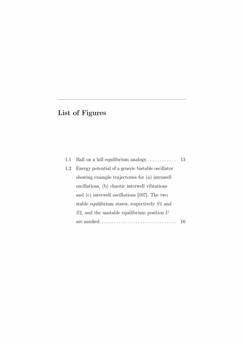
List of Figures
1.1 Ball on a hill equilibrium analogy. . . . . . . . . . . . 13
1.2 Energy potential of a generic bistable oscillator
showing example trajectories for (a) intrawell
oscillations, (b) chaotic interwell vibrations
and (c) interwell oscillations [107]. The two
stable equilibrium states, respectively S1 and
S2, and the unstable equilibrium position U
are marked. . . . . . . . . . . . . . . . . . . . . . . . . . . . . . . . 16
List of Figures
1.3 Restoring force for a generic bistable system.
The two stable equilibrium states, respectively
S1 and S2, and the unstable equilibrium
position U are marked. Critical force required
to switch from the first to second equilibrium
state, F12 , and from the second to the
first, F21, are marked. . . . . . . . . . . . . . . . . . . . . . 18
1.4 Example of displacement–time responses
(top row) and phase plots with an overlap
Poincaré map as black circles (bottom
row) for three dynamic regimes of bistable
oscillators, as reported in fig. 1.2: (a) and
(d) intrawell oscillations, (b) and (e) chaotic
interwell vibrations, (c) and (f) interwell
oscillations [107]. . . . . . . . . . . . . . . . . . . . . . . . . . . 20
1.5 Periodic driving signal causes the bistable
potential to be tilted back and forth,
antisymmetrically raising and lowering the left
and right potential wells during a period of
the driving signal. . . . . . . . . . . . . . . . . . . . . . . . . . 26
446
List of Figures
2.1 Schematic of the cross section of the
BESOI technology from Centro Nacional de
Microelectrónica (CNM) of Barcelona. Layers
on the top of the mechanical structure layer
are generically indicated as “other layers”. The
picture is not in scale. . . . . . . . . . . . . . . . . . . . . . . 48
2.2 SEM image of the SOI substrate used in the
BESOI process. Roughness in the etched
sidewalls of the silicon substrate is due to the
RIE. . . . . . . . . . . . . . . . . . . . . . . . . . . . . . . . . . . . . . 49
2.3 SEM image of a nonlinear fully compliant
structure released in the BESOI process. . . . . . . 51
2.4 Schematic of the cross section of the
MetalMUMPs® process provided by
MEMSCAPTM [62]. The picture is not in scale. 53
2.5 SEM image of some microdevices realized
in the MetalMUMPs® process provided by
MEMSCAPTM. . . . . . . . . . . . . . . . . . . . . . . . . . . . . 55
447
List of Figures
2.6 Schematic of the cross section of the
PiezoMUMPs® process provided by
MEMSCAPTM [63]. The picture is not in scale. 57
2.7 A die with several devices such as cantilever
beams and nonlinear test structures designed
at the Nanotechlab of the University of
Catania (Italy) and fabricated in the
PiezoMUMPs® process at MEMSCAPTM. . . . . 59
2.8 Schematic of the cross section of the
ThELMA® process from STMicroelectronics
(courtesy of the STMicroelectronics of
Castelletto, Italy). The picture is not in scale. . 61
2.9 SEM pictures of some devices
in the ThELMA® process from
STMicroelectronics [135, 242]. . . . . . . . . . . . . . . . 63
2.10 Schematic of the cross section of the RTI 5µ®
process from Radiant (courtesy of Radiant
inc.). The picture is not in scale. . . . . . . . . . . . . . 65
2.11 SEM picture of the resulting cross section
from the RTI 5µ® process from Radiant. . . . . . 66
448
List of Figures
2.12 Optical microscope image of a ferroelectric
capacitor in the RTI 5µ® process from
Radiant. The same kind of capacitors will be
recycled to build prototypes of piezoelectric
nano-cantilever beams through FIB milling in
subsection 2.2.1. . . . . . . . . . . . . . . . . . . . . . . . . . . . 67
2.13 First step of process of releasing a cantilever
beam through FIB milling (SEM picture). . . . . 76
2.14 Tip of the cantilever beam just before its
release (SEM picture). . . . . . . . . . . . . . . . . . . . . . . 78
2.15 Tip of the cantilever beam after its release
(SEM picture). . . . . . . . . . . . . . . . . . . . . . . . . . . . . 79
2.16 SEM picture of the finally released cantilever
beam along with its sizes in length and width
(tilt correction has been taken into account).
A slight curvature in the out-of-plane direction
is caused by the residual stress inside the
structure due to the Radiant process. . . . . . . . . . 80
449
List of Figures
2.17 SEM picture of the finally released cantilever
beam along with its sizes in thickness (tilt
correction has been taken into account). . . . . . . 81
2.18 SEM picture illustrating the position of
released cantilever beam inside the die
previously used as ferroelectric capacitor.
The areas occupied by the layers of the
piezoelectric stack (top electrode, PZT and
bottom electrode) are distinguished by the
different shades of gray and indicated in the
image for the sake of clearness. . . . . . . . . . . . . . . 82
2.19 SEM picture of a polished cantilever beam
along with its sizes in length and width (tilt
correction has been taken into account). . . . . . . 84
2.20 SEM picture of a polished cantilever beam
along with its sizes in thickness (tilt correction
has been taken into account). . . . . . . . . . . . . . . . 85
2.21 Schematic representing the process of ablation
of the target material in the PPD. . . . . . . . . . . . 88
450
List of Figures
2.22 Picture of the components of the PPD along
with the pulsed plasma and the plume during
a material deposition. . . . . . . . . . . . . . . . . . . . . . . 89
2.23 SEM picture showing the surface morphology
of the deposited ZnO film. . . . . . . . . . . . . . . . . . . 93
2.24 SEM picture showing a cross section of the
deposited ZnO film. Top brighter layer is the
deposited ZnO film and the bottom darker
layer is the silicon substrate. This cross section
has been realized through FIB milling. . . . . . . . 94
2.25 Relation between the number of plasma pulses
in a single deposition and the final thickness
of the deposited ZnO film, as resulting from
the characterization of the depositions samples. 95
2.26 RBS spectrum obtained from ZnO film
characterization. Peaks of the element zinc
and of the element oxygen are detected and
the stoichiometric ratio is derived from data
elaborations. . . . . . . . . . . . . . . . . . . . . . . . . . . . . . . 97
451
List of Figures
2.27 XRD detector scan spectra comparison of three
ZnO samples deposited at different substrate
temperatures. Crystalline orientations
observed are indicated in the plot. . . . . . . . . . . . 98
2.28 XRD rocking curves comparison of two ZnO
samples deposited at substrate temperatures
respectively of 400℃ and 600℃. . . . . . . . . . . . . . 99
2.29 SEM picture showing the surface morphology
and the typical thickness of the metal ink (left
upper side of the picture) after its deposition
through the inkjet printer on the plastic
flexible substrate (right lower side of the
picture). . . . . . . . . . . . . . . . . . . . . . . . . . . . . . . . . . . 107
452
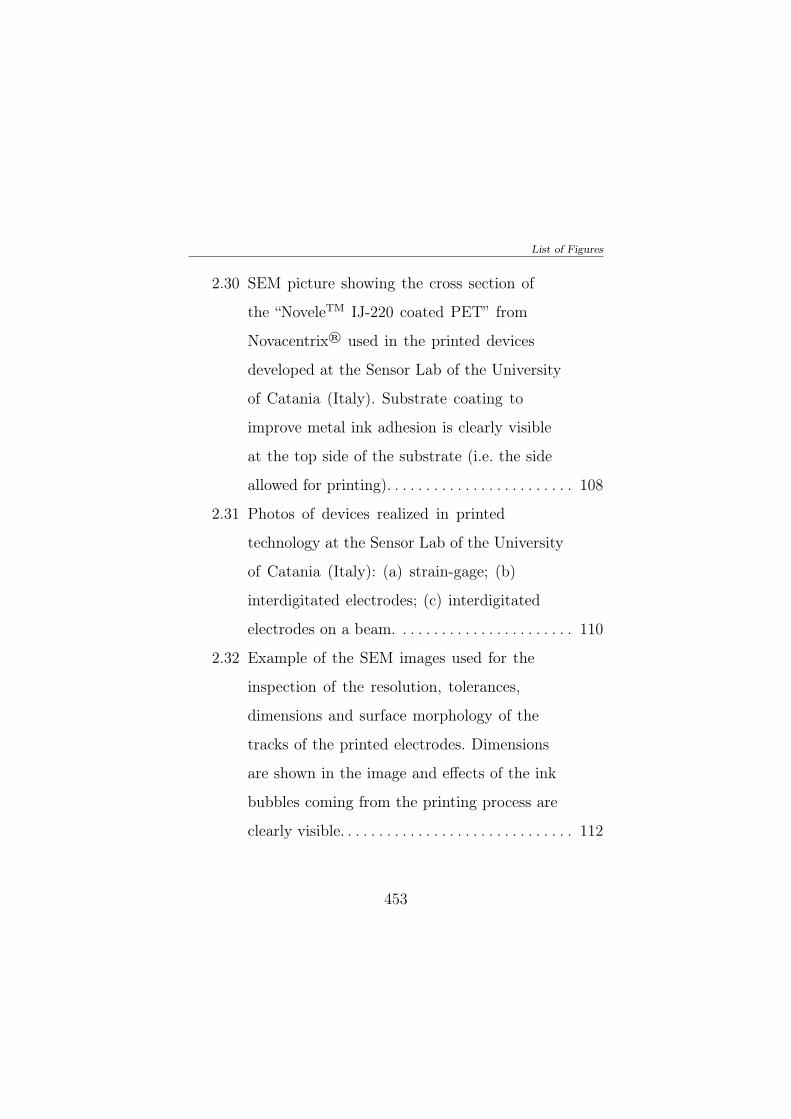
List of Figures
2.30 SEM picture showing the cross section of
the “NoveleTM IJ-220 coated PET” from
Novacentrix® used in the printed devices
developed at the Sensor Lab of the University
of Catania (Italy). Substrate coating to
improve metal ink adhesion is clearly visible
at the top side of the substrate (i.e. the side
allowed for printing). . . . . . . . . . . . . . . . . . . . . . . . 108
2.31 Photos of devices realized in printed
technology at the Sensor Lab of the University
of Catania (Italy): (a) strain-gage; (b)
interdigitated electrodes; (c) interdigitated
electrodes on a beam. . . . . . . . . . . . . . . . . . . . . . . 110
2.32 Example of the SEM images used for the
inspection of the resolution, tolerances,
dimensions and surface morphology of the
tracks of the printed electrodes. Dimensions
are shown in the image and effects of the ink
bubbles coming from the printing process are
clearly visible. . . . . . . . . . . . . . . . . . . . . . . . . . . . . . 112
453
List of Figures
3.1 Plot of the power consumption of several target
devices for energy harvesting applications
compared with power available from batteries
and power scavenged by energy harvesters in
actual technologies [108]. . . . . . . . . . . . . . . . . . . . 116
3.2 Time series of the acceleration coming from
the footsteps of a walking person, measured
through an accelerometer placed near the heel. 125
3.3 Time series of the acceleration coming from
the footsteps of a running person, measured
through an accelerometer placed near the heel. 125
3.4 Vibration spectra for a microwave oven and
office windows next to a busy street [202]. . . . . . 128
3.5 General architecture of devices for energy
harvesting from mechanical vibrations. . . . . . . . 130
3.6 Schematization of a cantilever beam having
a proof mass on its free end (left) and
of the 1 degree-of-freedom second order
mass-damper-stiffness model (right). . . . . . . . . . 133
454
List of Figures
3.7 Example of the frequency spectrum of the
power harvested by a linear resonant system
for different values of the damping ratio ζ [58]. 135
3.8 (a) Resonant frequency tuning of a clamped-
clamped beam through axial preload [138].
(b) Resonant frequency shift after tensile and
compressive axial preload of clamped-clamped
beam [138]. (c) Example of structure
exploiting electrostatic spring softening to
tune resonant frequency [1]. (d) Resonant
frequency tuning through magnetic levitation
forces [48]. . . . . . . . . . . . . . . . . . . . . . . . . . . . . . . . . 140
3.9 (a) Array of linear resonant structures [214].
(b) Frequency spectrum of the output from
an array of linear resonant structures [214].
(c) Cantilever beam with amplitude
limiter [145]. (d) Nonlinearities in spring
stiffness and damping introduced by
mechanical stoppers [145]. . . . . . . . . . . . . . . . . . . 143
455
List of Figures
3.10 Example of the frequency response function
for the Duffing oscillator in terms of amplitude
A and phase φ. The solid and dotted lines
correspond to the stable and unstable
equilibria, respectively. When a = 0, the
frequency response function shows a peak of
the usual resonance at ω ≈ ω0, and, when
a 6= 0 , this peak is curved. For a hardening
spring (a < 0), the peak curves to the
right, and to the left for a softening spring
(a > 0) [113]. . . . . . . . . . . . . . . . . . . . . . . . . . . . . . 147
3.11 Example of foldover effect in the frequency
response of an inverted pendulum [77]. . . . . . . . 149
3.12 Example of superharmonic resonace in an
inverted pendulum [228]. . . . . . . . . . . . . . . . . . . . 150
3.13 Example of devices adopting nonlinear springs
in their mechanical coupling structure that
have been proposed in literature: (a) [168],
(b) [152], (c) [237] and (d) [166]. . . . . . . . . . . . . . 152
456
List of Figures
3.14 Strategies to implement bistability in energy
harvesters [107]: (a) magnetic attraction,
(b) magnetic repulsion and (c) mechanical
bistability. . . . . . . . . . . . . . . . . . . . . . . . . . . . . . . . . 156
3.15 Direct and converse effect in piezoelectric
materials. . . . . . . . . . . . . . . . . . . . . . . . . . . . . . . . . 158
3.16 Classification of piezoelectric materials. . . . . . . . 160
3.17 d33 mode and d31 mode in piezoelectric devices. 161
3.18 Electrodes configurations to exploit d33 mode
and d31 mode in cantilever beams. . . . . . . . . . . . 163
3.19 Configuration of integrated capacitors for
electrostatic energy harvesters: (a) in-plane
overlap variable capacitors, (b) in-plane gap
closing capacitors and (c) out-of-plane gap
closing capacitors. . . . . . . . . . . . . . . . . . . . . . . . . . 170
3.20 Circuit used in the switching mode operation
of electrostatic transducer . . . . . . . . . . . . . . . . . . 174
457
List of Figures
3.21 Switching operating modes cycles for
electrostatic mechanical to electrical
transducers: (a) constant voltage, (b) constant
charge. In both graphs, the x-axis represents
voltages and the y-axis charges. . . . . . . . . . . . . . 175
3.22 Electret based harvester using a cantilever
beam as mechanical coupling structure [32]. . . . 181
3.23 Two-dimensional structure of the proposed
device to be realized in the BESOI process. . . . 188
3.24 The initial position (S1’) is shown together
with the unstable (U) and the second stable
equilibrium position (S2) as resulting from
FEM simulations. . . . . . . . . . . . . . . . . . . . . . . . . . . 189
3.25 Pseudo-rigid body model of the microstructure.
The terms K1 and K2 refer to (3.20), and Ksb
to the (3.21). . . . . . . . . . . . . . . . . . . . . . . . . . . . . . . 191
3.26 Basic schematic of the variables listed in the
tab. 3.4 for the microstructure in fig. 3.23.
The picture is not in scale. . . . . . . . . . . . . . . . . . . 195
458
List of Figures
3.27 Elastic potential energy evaluated by PRBM
with θ0=5.5°. The stables, S1 and S2, and the
unstable U equilibrium positions are marked. . . 195
3.28 Elastic potential energy evaluated for different
values of the parameter θ0. For θ0=4° and
the other parameters in table 3.4, the
microstructure has a monostable behaviour.
Results refer to parameters different from
those in the tab. 3.4. . . . . . . . . . . . . . . . . . . . . . . . 197
3.29 Reaction force on central mass after
displacement numerically evaluated by FEM. . . 198
3.30 Elastic potential energy numerically evaluated
by FEM (dashed line) compared with the
potential (continuous line) obtained from
PRBM (fig. 3.27). . . . . . . . . . . . . . . . . . . . . . . . . . 199
3.31 Time series of the central mass displacement
as resulting from the numerical evaluation of
SDEs model by Euler-Maruyama method. . . . . . 202
459
List of Figures
3.32 Trajectory map of the two system states
variables (displacement and velocity) under
stochastic input dWt, as resulting from the
numerical evaluation of SDEs model by
Euler-Maruyama method. . . . . . . . . . . . . . . . . . . . 202
3.33 Comparison between power spectrum densities
of central mass displacements of bistable
microstructure and monostable one under the
same stochastic stimulus dWt. . . . . . . . . . . . . . . . 204
3.34 Basic illustration of the substitutions, only
for the left side, made to the microstructure
in fig. 3.23 in order to make it more flexible.
Changes and nomenclature are analogous on
the right side. . . . . . . . . . . . . . . . . . . . . . . . . . . . . . 207
3.35 Three-dimensional model of the new proposed
microstructure. . . . . . . . . . . . . . . . . . . . . . . . . . . . . 209
3.36 Basic schematic of the variables listed in the
tab. 3.5 for the microstructure in fig. 3.35.
The picture is not in scale. . . . . . . . . . . . . . . . . . . 211
460
List of Figures
3.37 Reaction force (dashed line) on central mass
and elastic potential energy (continuous
line) evaluated by FEA for configuration on
table 3.5 of the microstructure proposed in
figure 3.35. Equilibrium positions are indicated. 212
3.38 Results from several stochastic analyses for
accelerations having different RMS values.
Points represent the mean values of the
number of commutations between stable
equilibrium states in a time interval of 60 s
and 30 simulations for each simulated value of
input peak accelerations; while “x” represents
the standard deviation. . . . . . . . . . . . . . . . . . . . . . 213
3.39 Elastic potential energy numerically evaluated
by FEM of the monostable device (dashed
line) compared with the elastic potential
(continuous line) of the bistable one. . . . . . . . . . 214
461
List of Figures
3.40 Simulation results: plot of PSD of central
mass displacement for the bistable (blue
curve) and the monostable (yellow curve)
in the case of under-threshold excitation
(acceleration peak value of about 4 m/s2 when
the bistable system oscillates around its first
stable equilibrium state. . . . . . . . . . . . . . . . . . . . . 215
3.41 Simulation results: plot of PSD of central mass
displacement for the bistable (blue curve) and
the monostable (yellow curve) in the case of
underthreshold excitation (acceleration peak
value of about 13 m/s2 when the bistable
system oscillates around its first stable
equilibrium state. . . . . . . . . . . . . . . . . . . . . . . . . . . 216
462
List of Figures
3.42 Energy of central mass displacements
normalized with input energy from vibrations
versus the RMS value of the input acceleration
signal. Points represent the computed values
for the bistable microstructure at each
acceleration peak value, while the “x” for the
monostable device. . . . . . . . . . . . . . . . . . . . . . . . . . 217
3.43 Three dimensional model of the device
incorporating the microstructure in fig. 3.35
and the mechanical-to-electrical transduction
mechanism. The letters “A”, “B” and “C”
indicate the pads for the electrical connection
of the plates of the interdigitated capacitors. . . 219
3.44 Basic conceptual schematic of the proposed
modifications in the BESOI technology.
“A”and “C” represent areas at different electric
potential. The picture is not in scale. . . . . . . . . . 224
463
List of Figures
3.45 Power harvested at several RMS value of input
acceleration for the bistable device and its
“equivalent” monostable one. A polarization
voltage of 30 V and the parameters for the
transduction mechanism in the tab. 3.6, with
tf = 465 µm, are considered. . . . . . . . . . . . . . . . . 227
3.46 3D model of the proposed mechanical structure
in the STMicroelectronics ThELMA® process. 230
3.47 Flexural beams of the proposed mechanical
structure in the STMicroelectronics
ThELMA® process. Their shape is the same
as the one of the device in the BESOI process
in subsection 3.2.3 but their positioning within
the structure changes. . . . . . . . . . . . . . . . . . . . . . . 231
3.48 Reaction forces along y-axis versus device
mass displacement along y-axis as resulting
from FEM simulations. . . . . . . . . . . . . . . . . . . . . . 234
3.49 Elastic potential energy numerically evaluated
through numerical integration of FEM
analyses results in fig. 3.48. . . . . . . . . . . . . . . . . . 235
464

List of Figures
3.50 Elastic potential energy numerically evaluated
from FEM analyses for different values of the
angle θ0. . . . . . . . . . . . . . . . . . . . . . . . . . . . . . . . . . . 236
3.51 Comb electrodes designed on the
microstructure in fig. 3.46. . . . . . . . . . . . . . . . . . . 237
3.52 Comparison in the power output estimation
between the bistable device and its
“equivalent” monostable for different values
of the polarization voltage, when an input
acceleration aext having an RMS value of
7 m/s2 and a bandwidth of 500 Hz is applied
and an amplitude threshold of 18 µm is
adopted in the monostable device. . . . . . . . . . . . 242
3.53 Layout of the cascaded triple bent-beam
microstructure with the definition of its
geometric specifications, whose values and
descriptions are listed in the tab. 3.13. . . . . . . . . 244
3.54 3D model of cascaded triple bent-beam
microstructure. . . . . . . . . . . . . . . . . . . . . . . . . . . . . 246
465
List of Figures
3.55 Reaction forces along y-axis versus device
shuttle displacement along y-axis as resulting
from FEM simulations. . . . . . . . . . . . . . . . . . . . . . 247
3.56 Elastic potential energy numerically evaluated
from FEM analyses results in fig. 3.55). . . . . . . . 248
3.57 Deformed shapes of the microstructure in
its unstable (left) and second stable (right)
equilibrium positions, as computed in the
FEM simulations. Both deformed shapes are
compared with the undeformed shape (i.e. the
fabrication position). . . . . . . . . . . . . . . . . . . . . . . . 249
3.58 Optical microscope pictures of the two
stable equilibrium positions of the device, as
resulting from its test at the Nanotechlab of
the University of Catania (Italy). The probe
used for the device shuttle actuation is barely
visible out-of-focus in the upper side of both
pictures, as it does not touch the device. . . . . . . 250
466
List of Figures
3.59 (a) Ideal buckled beam (“Mode 1”) subject to
residual stress, showing two possible states.
(b) Ideal buckled beam subject to a critical
load Pcr or displacement ∆cr. (c) Ideal (and
unlikely) “Mode 0” transition (or supercritical
buckling) between buckled positions. (d)
“Mode 2” transition between buckled positions,
with rotation of center point. (e) “Mode 3”
transition is made possible by the addition
of multiple beams and central shuttle for
symmetry. . . . . . . . . . . . . . . . . . . . . . . . . . . . . . . . . 253
3.60 Picture of the realized prototype in its upper
stable equilibrium state and fixed at both ends
by the clamping system. Length and width
of the device in the picture are respectively
10 cm and 1 cm. . . . . . . . . . . . . . . . . . . . . . . . . . . . 257
3.61 Diagram (not in scale) of the device layers
compared with a picture of the device in
fig. 3.60. . . . . . . . . . . . . . . . . . . . . . . . . . . . . . . . . . . 258
467
List of Figures
3.62 Diagram summarizing the design flow of the
device. . . . . . . . . . . . . . . . . . . . . . . . . . . . . . . . . . . . 261
3.63 Experimental setup for the mechanical
characterization of the reaction forces of the
buckled beam. . . . . . . . . . . . . . . . . . . . . . . . . . . . . 262
3.64 Measurement results of the reaction forces
in the out-of-plane direction for a beam
10 cm long and 1 cm wide subjected to a
displacement precompression ∆Y of 2.7 mm.
Results refers to the stable zones of the beam. . 263
3.65 Measurement results and FEM simulations
results of the relation between the applied
displacement precompressions ∆Y and the
distance ∆X between stable equilibrium states
for a beam 10 cm long and 1 cm wide. . . . . . . . . 264
468
List of Figures
3.66 Experimental setup of the mechanical
characterization of the relation between the
distance ∆X between stable equilibrium states
and the minimum required static acceleration
aext for achieving device commutations. Proof
mass is represented by a steel dice attached to
the centre of the beam. . . . . . . . . . . . . . . . . . . . . . 265
3.67 Measurement results of the static relation
between the distance ∆X between stable
equilibrium states and the minimum required
static acceleration aext for achieving device
commutations for a beam 10 cm long and
1 cm wide. . . . . . . . . . . . . . . . . . . . . . . . . . . . . . . . . 266
3.68 Experimental setup for the electrical
characterization of the device. . . . . . . . . . . . . . . . 268
3.69 Output voltage of a beam 10 cm long and
1 cm wide subjected to a displacement
precompression ∆Y of 3 mm and forced by a
periodic mechanical burst having a frequency
of 1 Hz. . . . . . . . . . . . . . . . . . . . . . . . . . . . . . . . . . . 269
469

List of Figures
3.70 Output voltage of a beam 10 cm long and
1 cm wide subjected to a displacement
precompression ∆Y of 3 mm and forced by a
periodic mechanical burst having a frequency
of 10 Hz. . . . . . . . . . . . . . . . . . . . . . . . . . . . . . . . . . 270
3.71 Output voltage of a beam 10 cm long and
1 cm wide subjected to a displacement
precompression ∆Y of 3 mm and forced by a
periodic mechanical burst having a frequency
of 30 Hz. . . . . . . . . . . . . . . . . . . . . . . . . . . . . . . . . . 271
3.72 Output voltage of a beam 10 cm long and
1 cm wide subjected to a displacement
precompression ∆Y of 3 mm and forced by a
periodic mechanical burst having a frequency
of 70 Hz. . . . . . . . . . . . . . . . . . . . . . . . . . . . . . . . . . 272
470
List of Figures
3.73 Waveforms of the applied mechanical
burst (as resulting from the accelerometer
measurement) and of the displacement of
the centre of the beam (as resulting from
the laser measurement) when the device is
forced by a periodic mechanical burst having
a frequency of 10 Hz. Units on y-axes are
reported in voltage (i.e. the direct output from
the accelerometer and from the laser distance
meter. A beam 10 cm long and 1 cm wide
subjected to a displacement precompression
∆Y of 3 mm has been considered. . . . . . . . . . . . 273
3.74 RMS value of the output voltage of a beam
10 cm long and 1 cm wide subjected to a
displacement precompression ∆Y of 3 mm
forced by a periodic mechanical burst having
several frequencies and several amplitudes Ab. . 274
4.1 General schemes of current sensing techniques:
(a) current transformer, (b) Hall Effect, (c)
Rogowski coil and (d) fluxgate magnetometer. . 282
471
List of Figures
4.2 Schematic of a piezoelectric resonant AC
current sensor proposed in literature [137]. . . . . 287
4.3 Schematic of the proposed nonlinear AC
current sensor. . . . . . . . . . . . . . . . . . . . . . . . . . . . . 288
4.4 Schematic representation of the spatial
positions of the vectors in (4.6). The image is
not in scale. . . . . . . . . . . . . . . . . . . . . . . . . . . . . . . . 298
4.5 3D model of the cantilever beam designed
to implement the AC current microsensor
proposed in this work. The two top electrodes
are connected in short circuit in this device
and considered as a single electrode. . . . . . . . . . . 305
4.6 Comparison of four bistable magneto-elastic
potentials U(z), computed through (4.10) and
the parameter values in section 4.4, obtained
with four different values of the distance ∆
(2.1 mm, 2.2 mm, 2.25 mm, 2.3 mm). . . . . . . . . 309
4.7 Time series of the input acceleration aext
having a RMS value of 0.031g. . . . . . . . . . . . . . . 312
472
List of Figures
4.8 PSD of the input acceleration aext having a
RMS value of 0.031g. . . . . . . . . . . . . . . . . . . . . . . . 312
4.9 Time series of the input acceleration aext
having a RMS value of 0.31g. . . . . . . . . . . . . . . . 313
4.10 PSD of the input acceleration aext having a
RMS value of 0.31g. . . . . . . . . . . . . . . . . . . . . . . . . 313
4.11 Time series of the input acceleration aext
having a RMS value of 0.98g. . . . . . . . . . . . . . . . 314
4.12 PSD of the input acceleration aext having a
RMS value of 0.98g. . . . . . . . . . . . . . . . . . . . . . . . . 314
4.13 Mean number of commutations in 1 s, over 30
simulations, versus AC current magnitude at
a frequency of 50 Hz, when the RMS value
of input acceleration aext is 0.031g, for four
values of the distance ∆ (2.1 mm, 2.2 mm,
2.25 mm, 2.3 mm). . . . . . . . . . . . . . . . . . . . . . . . . 316
473
List of Figures
4.14 Mean number of commutations in 1 s, over 30
simulations, versus AC current magnitude at
a frequency of 50 Hz, when the RMS value of
input acceleration aext is 0.16g, for four values
of the distance ∆ (2.1 mm, 2.2 mm, 2.25 mm,
2.3 mm). . . . . . . . . . . . . . . . . . . . . . . . . . . . . . . . . . 317
4.15 Mean number of commutations in 1 s, over 30
simulations, versus AC current magnitude at
a frequency of 50 Hz, when the RMS value of
input acceleration aext is 0.31g, for four values
of the distance ∆ (2.1 mm, 2.2 mm, 2.25 mm,
2.3 mm). . . . . . . . . . . . . . . . . . . . . . . . . . . . . . . . . . 318
4.16 Mean number of commutations in 1 s, over 30
simulations, versus AC current magnitude at
a frequency of 50 Hz, when the RMS value of
input acceleration aext is 0.91g, for four values
of the distance ∆ (2.1 mm, 2.2 mm, 2.25 mm,
2.3 mm). . . . . . . . . . . . . . . . . . . . . . . . . . . . . . . . . . 319
474
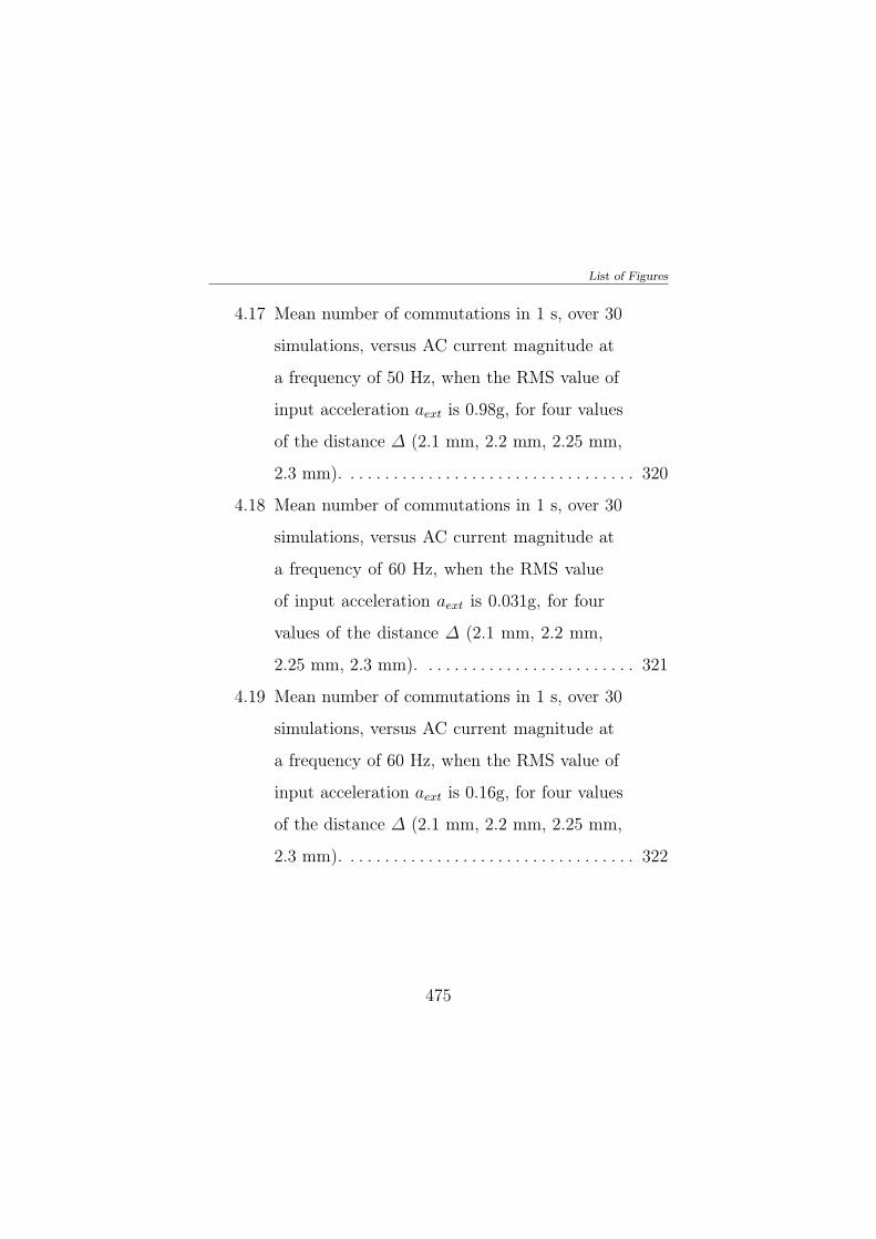
List of Figures
4.17 Mean number of commutations in 1 s, over 30
simulations, versus AC current magnitude at
a frequency of 50 Hz, when the RMS value of
input acceleration aext is 0.98g, for four values
of the distance ∆ (2.1 mm, 2.2 mm, 2.25 mm,
2.3 mm). . . . . . . . . . . . . . . . . . . . . . . . . . . . . . . . . . 320
4.18 Mean number of commutations in 1 s, over 30
simulations, versus AC current magnitude at
a frequency of 60 Hz, when the RMS value
of input acceleration aext is 0.031g, for four
values of the distance ∆ (2.1 mm, 2.2 mm,
2.25 mm, 2.3 mm). . . . . . . . . . . . . . . . . . . . . . . . . 321
4.19 Mean number of commutations in 1 s, over 30
simulations, versus AC current magnitude at
a frequency of 60 Hz, when the RMS value of
input acceleration aext is 0.16g, for four values
of the distance ∆ (2.1 mm, 2.2 mm, 2.25 mm,
2.3 mm). . . . . . . . . . . . . . . . . . . . . . . . . . . . . . . . . . 322
475

List of Figures
4.20 Mean number of commutations in 1 s, over 30
simulations, versus AC current magnitude at
a frequency of 60 Hz, when the RMS value of
input acceleration aext is 0.31g, for four values
of the distance ∆ (2.1 mm, 2.2 mm, 2.25 mm,
2.3 mm). . . . . . . . . . . . . . . . . . . . . . . . . . . . . . . . . . 323
4.21 Mean number of commutations in 1 s, over 30
simulations, versus AC current magnitude at
a frequency of 60 Hz, when the RMS value of
input acceleration aext is 0.91g, for four values
of the distance ∆ (2.1 mm, 2.2 mm, 2.25 mm,
2.3 mm). . . . . . . . . . . . . . . . . . . . . . . . . . . . . . . . . . 324
4.22 Mean number of commutations in 1 s, over 30
simulations, versus AC current magnitude at
a frequency of 60 Hz, when the RMS value of
input acceleration aext is 0.98g, for four values
of the distance ∆ (2.1 mm, 2.2 mm, 2.25 mm,
2.3 mm). . . . . . . . . . . . . . . . . . . . . . . . . . . . . . . . . . 325
476
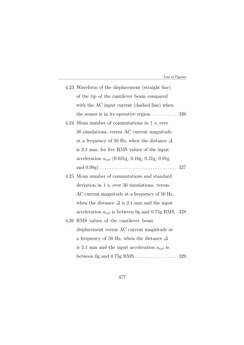
List of Figures
4.23 Waveform of the displacement (straight line)
of the tip of the cantilever beam compared
with the AC input current (dashed line) when
the sensor is in its operative region. . . . . . . . . . . 326
4.24 Mean number of commutations in 1 s, over
30 simulations, versus AC current magnitude
at a frequency of 50 Hz, when the distance ∆
is 2.1 mm, for five RMS values of the input
acceleration aext (0.031g, 0.16g, 0.31g, 0.91g
and 0.98g). . . . . . . . . . . . . . . . . . . . . . . . . . . . . . . . 327
4.25 Mean number of commutations and standard
deviation in 1 s, over 30 simulations, versus
AC current magnitude at a frequency of 50 Hz,
when the distance ∆ is 2.1 mm and the input
acceleration aext is between 0g and 0.75g RMS. 328
4.26 RMS values of the cantilever beam
displacement versus AC current magnitude at
a frequency of 50 Hz, when the distance ∆
is 2.1 mm and the input acceleration aext is
between 0g and 0.75g RMS. . . . . . . . . . . . . . . . . . 329
477
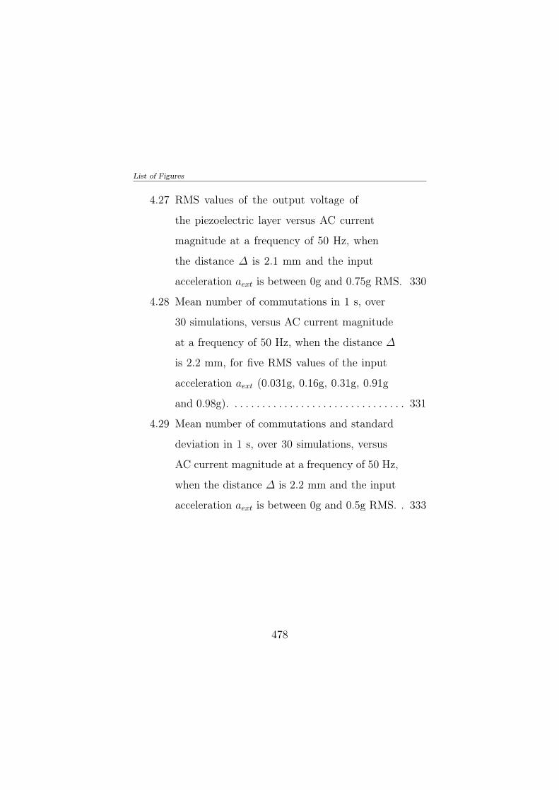
List of Figures
4.27 RMS values of the output voltage of
the piezoelectric layer versus AC current
magnitude at a frequency of 50 Hz, when
the distance ∆ is 2.1 mm and the input
acceleration aext is between 0g and 0.75g RMS. 330
4.28 Mean number of commutations in 1 s, over
30 simulations, versus AC current magnitude
at a frequency of 50 Hz, when the distance ∆
is 2.2 mm, for five RMS values of the input
acceleration aext (0.031g, 0.16g, 0.31g, 0.91g
and 0.98g). . . . . . . . . . . . . . . . . . . . . . . . . . . . . . . . 331
4.29 Mean number of commutations and standard
deviation in 1 s, over 30 simulations, versus
AC current magnitude at a frequency of 50 Hz,
when the distance ∆ is 2.2 mm and the input
acceleration aext is between 0g and 0.5g RMS. . 333
478
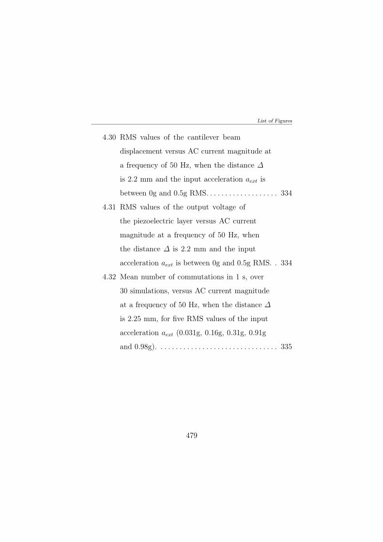
List of Figures
4.30 RMS values of the cantilever beam
displacement versus AC current magnitude at
a frequency of 50 Hz, when the distance ∆
is 2.2 mm and the input acceleration aext is
between 0g and 0.5g RMS. . . . . . . . . . . . . . . . . . . 334
4.31 RMS values of the output voltage of
the piezoelectric layer versus AC current
magnitude at a frequency of 50 Hz, when
the distance ∆ is 2.2 mm and the input
acceleration aext is between 0g and 0.5g RMS. . 334
4.32 Mean number of commutations in 1 s, over
30 simulations, versus AC current magnitude
at a frequency of 50 Hz, when the distance ∆
is 2.25 mm, for five RMS values of the input
acceleration aext (0.031g, 0.16g, 0.31g, 0.91g
and 0.98g). . . . . . . . . . . . . . . . . . . . . . . . . . . . . . . . 335
479
List of Figures
4.33 Mean number of commutations and standard
deviation in 1 s, over 30 simulations, versus
AC current magnitude at a frequency of 50 Hz,
when the distance ∆ is 2.25 mm and the input
acceleration aext is between 0g and 0.4g RMS. . 337
4.34 RMS values of the cantilever beam
displacement versus AC current magnitude at
a frequency of 50 Hz, when the distance ∆
is 2.25 mm and the input acceleration aext is
between 0g and 0.5g RMS. . . . . . . . . . . . . . . . . . . 338
4.35 RMS values of the output voltage of
the piezoelectric layer versus AC current
magnitude at a frequency of 50 Hz, when
the distance ∆ is 2.25 mm and the input
acceleration aext is between 0g and 0.5g RMS. . 338
480
List of Figures
4.36 Mean number of commutations in 1 s, over
30 simulations, versus AC current magnitude
at a frequency of 50 Hz, when the distance ∆
is 2.3 mm, for five RMS values of the input
acceleration aext (0.031g, 0.16g, 0.31g, 0.91g
and 0.98g). . . . . . . . . . . . . . . . . . . . . . . . . . . . . . . . 340
4.37 Mean number of commutations and standard
deviation in 1 s, over 30 simulations, versus
AC current magnitude at a frequency of 50 Hz,
when the distance ∆ is 2.3 mm and the input
acceleration aext is between 0g and 0.1g RMS. . 341
4.38 RMS values of the cantilever beam
displacement versus AC current magnitude at
a frequency of 50 Hz, when the distance ∆
is 2.3 mm and the input acceleration aext is
between 0g and 0.1g RMS. . . . . . . . . . . . . . . . . . . 342
481
List of Figures
4.39 RMS values of the output voltage of
the piezoelectric layer versus AC current
magnitude at a frequency of 50 Hz, when
the distance ∆ is 2.3 mm and the input
acceleration aext is between 0g and 0.1g RMS. . 342
4.40 Monostable linear resonant potential obtained
with ∆ = 2.3 mm. . . . . . . . . . . . . . . . . . . . . . . . . 343
4.41 Number of commutations (blue line) given by
the bistable device for ∆ = 2.1 mm versus
output RMS voltage (green line) from the
linear device. The level of mechanical noise
aext is 0.31g and the operative range of the
bistable device is indicated through vertical
dotted lines. . . . . . . . . . . . . . . . . . . . . . . . . . . . . . . 345
482
List of Figures
4.42 Number of commutations (blue line) given by
the bistable device for ∆ = 2.2 mm versus
output RMS voltage (green line) from the
linear device. The level of mechanical noise
aext is 0.31g and the operative range of the
bistable device is indicated through vertical
dotted lines. . . . . . . . . . . . . . . . . . . . . . . . . . . . . . . 346
4.43 Number of commutations (blue line) given by
the bistable device for ∆ = 2.25 mm versus
output RMS voltage (green line) from the
linear device. The level of mechanical noise
aext is 0.31g and the operative range of the
bistable device is indicated through vertical
dotted lines. . . . . . . . . . . . . . . . . . . . . . . . . . . . . . . 347
483
List of Figures
4.44 Number of commutations (blue line) given by
the bistable device for ∆ = 2.3 mm versus
output RMS voltage (green line) from the
linear device. The level of mechanical noise
aext is 0.031g and the operative range of the
bistable device is indicated through vertical
dotted lines. . . . . . . . . . . . . . . . . . . . . . . . . . . . . . . 348
4.45 Estimation of the power harvested by the
bistable device (for four different values of ∆,
2.1 mm, 2.2 mm, 2.25 mm and 2.3 mm) and
by linear resonant device (∆ = 2.1 mm) for
several values of AC current magnitude to be
measured and a mechanical noise of 0.16g. . . . . 350
4.46 Macroscale prototype of the cantilever beam
with permanent magnets. . . . . . . . . . . . . . . . . . . . 354
4.47 Transformer and potentiometer used to
generate the AC target current from mains
voltage at 220 V. . . . . . . . . . . . . . . . . . . . . . . . . . . 354
4.48 Picture of the measurement setup. . . . . . . . . . . . 355
484

List of Figures
4.49 Piezoelectric output voltage obtained from
the measurement setup when an AC current
magnitude of 1 A is considered and a
distance ∆ of 47 mm is applied. From
the analysis of these results, no beam
commutations are observed. . . . . . . . . . . . . . . . . . 357
4.50 Piezoelectric output voltage obtained from
the measurement setup when an AC current
magnitude of 3 A is considered and a
distance ∆ of 47 mm is applied. From the
analysis of these results, 9 beam commutations
between stable equilibrium states are observed
in a time interval of 20 s. . . . . . . . . . . . . . . . . . . . 358
4.51 Number of beam commutations between
stable equilibrium states in 20 s for different
AC current magnitudes when a distance ∆
of 47 mm is applied, , as resulting from the
analysis of the measured piezoelectric output
voltage. . . . . . . . . . . . . . . . . . . . . . . . . . . . . . . . . . . 359
485
List of Figures
4.52 RMS values of the measured piezoelectric
output voltage for different AC current
magnitudes when a distance ∆ of 47 mm is
considered. . . . . . . . . . . . . . . . . . . . . . . . . . . . . . . . 360
4.53 Number of beam commutations between
stable equilibrium states in 20 s for different
AC current magnitudes when a distance ∆
of 45 mm is applied, as resulting from the
analysis of the measured piezoelectric output
voltage. . . . . . . . . . . . . . . . . . . . . . . . . . . . . . . . . . . 361
4.54 Piezoelectric output voltage obtained from
the measurement setup when an AC current
magnitude of 3.75 A is considered and
a distance ∆ of 45 mm is applied. From
the analysis of these results, 10 beam
commutations between stable equilibrium
states are observed in a time interval of 20 s. . . 362
4.55 RMS values of the measured piezoelectric
output voltage for different AC current
magnitudes for the linear resonant sensor. . . . . . 363
486
List of Figures
4.56 Number of beam commutations between
stable equilibrium states in 20 s for different
AC current magnitudes when a distance ∆
of 47 mm is applied. Values of ∆I and
∆Comm47 used for the computing of the
device sensitivity Sbist% [47mm] are indicated. . . . 365
4.57 Number of beam commutations between
stable equilibrium states in 20 s for different
AC current magnitudes when a distance ∆
of 47 mm is applied. Values of ∆I and
∆Comm45 used for the computing of the
device sensitivity Sbist% [45mm] are indicated. . . . 365
4.58 RMS values of the measured piezoelectric
output voltage for different AC current
magnitudes for the linear resonant sensor.
Values of ∆I, ∆V1 and ∆V2 used for the
computing of the device sensitivity Slin% are
indicated. . . . . . . . . . . . . . . . . . . . . . . . . . . . . . . . . 366
487
List of Figures
4.59 Estimation of the power harvested by the
bistable device (with ∆ = 47 mm) and by
linear resonant device (with ∆ → +∞) for
several values of AC current magnitude to
be measured, as resulting from the set of
measurements carried out. . . . . . . . . . . . . . . . . . . 368
488

List of Tables
3.1 Comparison of power scavenging and energy
sources. The top part of the table contains
sources with a fixed level of power generation;
the bottom part of the table displays sources
with a fixed amount of energy storage [202]. . . . 119
3.2 Acceleration magnitude and frequency of
fundamental vibration mode for various
sources [202]. . . . . . . . . . . . . . . . . . . . . . . . . . . . . . . 127
3.3 Mechanical material properties of single
crystal silicon [213] in BESOI technology. . . . . . 193
List of Tables
3.4 Geometric parameters of the microstructure
in fig. 3.23. The microstructure is symmetric
along y-axis. A basic schematic of the variables
listed is shown in fig. 3.26. . . . . . . . . . . . . . . . . . . 194
3.5 Geometric parameters of the microstructure
in fig. 3.35. The microstructure is symmetric
along y-axis. A basic schematic of the variables
listed is shown in fig. 3.36. . . . . . . . . . . . . . . . . . . 210
3.6 Parameters of the adopted mechanical-to-
electrical transduction mechanism for the
device in fig. 3.43. Values are equal for both
the capacitances CAC and CBC . . . . . . . . . . . . . . . 223
3.7 Material properties of the epitaxial polysilicon
in ThELMA® process used in the FEM
simulations [225]. . . . . . . . . . . . . . . . . . . . . . . . . . . 231
3.8 Geometric parameters of the microstructure
in fig. 3.46. The microstructure is symmetric
along y-axis. A basic schematic of the variables
listed is shown in fig. 3.36. . . . . . . . . . . . . . . . . . . 233
490
List of Tables
3.9 Parameters of the adopted mechanical-to-
electrical transduction mechanism for the
device in fig. 3.51. . . . . . . . . . . . . . . . . . . . . . . . . . 238
3.10 Mean electrical power harvested by the system
and mean number of commutations between
stable equilibrium states (over 30 simulations)
for several values of the polarization voltage
Vin, when an air-gap of 1.1 µm and an input
acceleration aext having an RMS value of
7 m/s2 and a bandwidth of 500 Hz are applied
to the system. . . . . . . . . . . . . . . . . . . . . . . . . . . . . . 239
3.11 Mean electrical power harvested by the system
and mean number of commutations between
stable equilibrium states (over 30 simulations)
for several values of the polarization voltage
Vin, when an air-gap of 2 µm and an input
acceleration aext having an RMS value of
7 m/s2 and a bandwidth of 500 Hz are applied
to the system. . . . . . . . . . . . . . . . . . . . . . . . . . . . . . 240
491
List of Tables
3.12 Mean electrical power harvested by the system
and mean number of commutations between
stable equilibrium states (over 30 simulations)
for several values of the polarization voltage
Vin, when an air-gap of 3 µm and an input
acceleration aext having an RMS value of
7 m/s2 and a bandwidth of 500 Hz are applied
to the system. . . . . . . . . . . . . . . . . . . . . . . . . . . . . . 241
3.13 Geometric specifications of the cascaded triple
bent-beam microstructure defined in fig. 3.53.
Due to the symmetry of the device along
y-axis, values are equal for the left and the
right side of the microstructure. . . . . . . . . . . . . . 245
3.14 Material properties of the electroplated nickel
used in the FEM simulations. . . . . . . . . . . . . . . . 246
4.1 Material properties used in the design and
simulations of the AC microsensor [213]. . . . . . . 307
4.2 Data of the power required by the home
appliances studied [66]. . . . . . . . . . . . . . . . . . . . . . 322
492


