Embed Size (px)
Citation preview

1
Topological insulator Bi2Se3 thin films grown on double-layer graphene by
molecular beam epitaxy
Can-Li Song1,2, Yi-Lin Wang1, Ye-Ping Jiang1, 2, Yi Zhang1, Cui-Zu Chang1,2, Lili Wang1, Ke He1, Xi
Chen2, Jin-Feng Jia2, Yayu Wang2, Zhong Fang1, Xi Dai1, Xin-Cheng Xie1, Xiao-Liang Qi3,
Shou-Cheng Zhang3, Qi-Kun Xue1,2*, and Xucun Ma1*
1 Institute of Physics, Chinese Academy of Sciences, Beijing 100190, China
2 Department of Physics, Tsinghua University, Beijing 100084, China
3Department of Physics, Stanford University, Stanford, California 94305-4045, USA
Atomically flat thin films of topological insulator Bi2Se3 have been grown on
double-layer graphene formed on 6H-SiC(0001) substrate by molecular beam
epitaxy. By a combined study of reflection high energy electron diffraction and
scanning tunneling microscopy, we identified the Se-rich condition and
temperature criterion for layer-by-layer growth of epitaxial Bi2Se3 films. The
as-grown films without doping exhibit a low defect density of 1.0±0.2×10¹¹/cm2,
and become a bulk insulator at a thickness of 10 quintuple layers, as revealed by
in situ angle resolved photoemission spectroscopy measurement.

2
Three dimensional (3D) topological insulators (TIs) such as Bi2Se3 and Bi2Te3 are
characterized by a bulk energy gap of strong spin-orbit coupling origin and metallic
surface states protected by time-reversal symmetry.1-11 Without external doping, the
Fermi level (EF) of the materials resides in the bulk energy gap and thus only
intersects the Dirac cone topological surface states,1-6 which we call as “intrinsic” TI
hereafter. A major experimental breakthrough in the emerging field of TIs is the
material realization of high-quality single crystals by self-flux method.2,3,5,12 However,
as revealed by angle resolved photoemission spectroscopy (ARPES), the as-grown
samples without doping are not a bulk insulator, rather, an n-type doped
semiconductor,2,3,5,12 presumably due to Se (Te) vacancies and antisite defects.12-14
Further improvement in material quality via reducing/removing the Se (Te) vacancies
is limited: it requires significant bulk diffusion of Se (Te) atoms in the quartz tube
where the crystal forms, which is difficult because of the very volatile nature of Se or
Te molecules compared to Bi. To reduce the unwanted electron carriers and move the
EF into the gap, a great number of carriers of opposite sign were introduced by
extremely heavy doping with Sn atoms in Bi2Te35 and Ca atoms in Bi2Se3.3,12
In this work, we report molecular beam epitaxy (MBE) growth of high-quality
Bi2Se3 thin films on double-layer graphene formed on the commercial 6H-SiC(0001)
substrates. The double-layer graphene has a similar layered structure to Bi2Se3 and is
chemically inert due to the strong bonding of carbon atoms,15 which turns out to
greatly suppress interface reaction leading to atomically sharp interface between
Bi2Se3 and graphene. We identify the layer-by-layer growth conditions of Bi2Se3
3
immediately on graphene by real-time reflection high energy electron diffraction
(RHEED). In situ scanning tunneling microscope (STM) and ARPES measurements
show that the as-grown films by our method are indeed a bulk insulator when the
thickness is above 10 quintuple layers (QL). The resulting sharp interface can be
employed to study the interaction of the two distinct massless Dirac fermions in TI
and graphene, respectively.
Our MBE growth and characterization of Bi2Se3 thin films were conducted in an
ultrahigh vacuum (UHV) MBE-ARPES-STM combined system (Omicron) with a
base pressure of 1×10⁻¹⁰ Torr. The double-layer graphene was prepared on a
nitrogen-doped SiC(0001) substrate with a resistivity of ~0.1 Ω·cm using the
well-established recipe.16 High purity Bi (99.999%) and Se (99.999%) were
evaporated from standard Knudsen-cells. ARPES spectra were collected at room
temperature by a Gammadata Scienta SES-2002 analyzer with a HeI light source of
21.2eV. We also used a low temperature STM system to characterize the as-grown
films (Unisoku).17 An MBE chamber is attached to the STM system and Bi2Se3 films
were grown by using the same conditions mentioned above. STM images were taken
at 4.8 K at a constant current of 0.1nA with a polycrystalline W tip. The dI/dV
mapping was acquired using a lock-in technique with a bias modulation of 10mV at
987.5Hz.17
The optimal conditions for layer-by-layer growth of bulk insulating Bi2Se3 films
were established by a systematic investigation of the growth dynamics, surface
morphology and thickness-dependent electronic structure with RHEED, STM and
4
ARPES. Similar to those for GaAs18 and Bi2Te3,6 the optimal growth can be achieved
under Se-rich atmosphere (Se/Bi beam flux ratio θ ≥10) and TBi>Tsubstrate>TSe (TBi,
Tsubstrate and TSe are the Bi-cell, Se-cell and substrate temperatures, respectively). The
former not only assures nucleation of the Bi2Se3 phase than other phases, according to
the phase diagram,19 but also minimizes the formation of Se vacancy, which is
difficult in self-flux method.2,3,5,12 Under Se-rich condition, there always exist extra
Se molecules on the growing front. However, these molecules cannot be incorporated
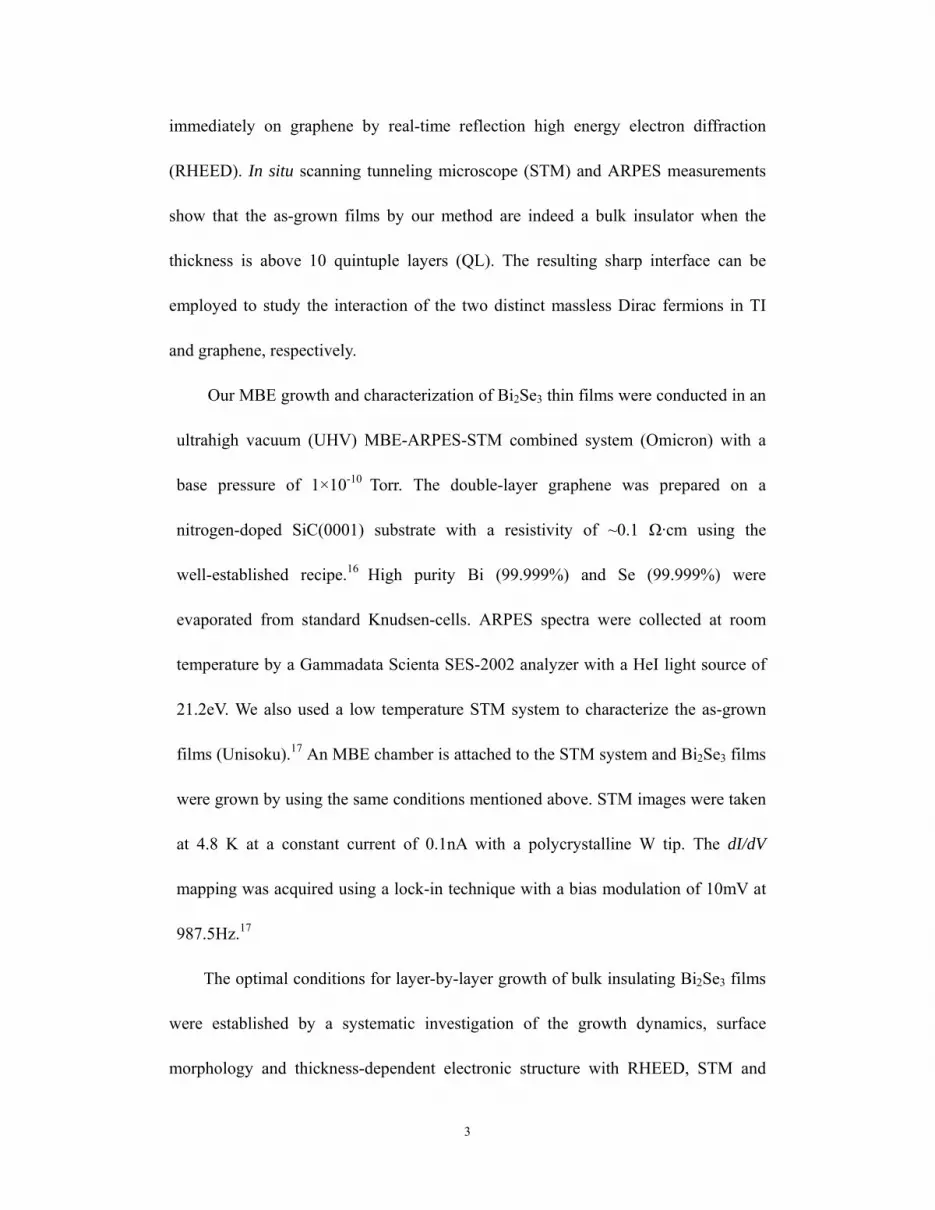
into the film and will desorb since Tsubstrate>TSe. The optimal growth is demonstrated
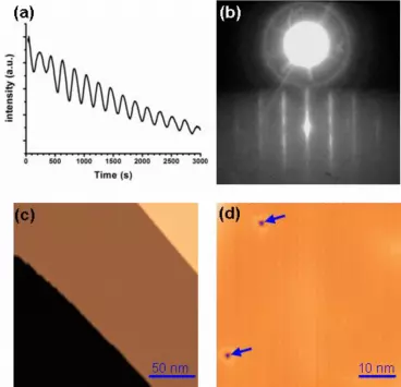
in Fig. 1. The film shown in this figure was grown at θ=11, TBi=550°C, TSe=136°C,
Tsubstrate=220°C and has a nominal thickness of 26 QL. The characteristic RHEED
intensity oscillation recorded during film deposition indicates an ideal layer-by-layer
growth (Fig. 1a), where each circle of the oscillations corresponds to deposition of
one QL of Bi2Se3. Therefore, the growth rate can be precisely measured, which is ~0.3
QL/min in this case. The atomically flat nature of the film is first evidenced by the
sharp 1×1 RHEED pattern in Fig. 1b and further demonstrated by the STM image in
Fig. 1c. As expected, the steps seen in the STM image have a height of 0.95 nm,
exactly the QL unit cell size of Bi2Se3 along the c axis.20 The Se-rich condition results
in very few defects in the as-grown samples. A typical STM image of the film is
shown in Fig. 1d. Only two defects can be found in an area of 50×50 nm2. The
dominant defects are Se vacancies (the dark depressions in Fig. 1d), which can be
identified by their registry with respect to the topmost Se lattice. The areal defect
density in this sample is ~1.0±0.2×10¹¹/cm2, which is much lower than that on the
5
cleaved samples.12 Further investigation indicates fewer vacancy defects if higher
Se/Bi flux ratio is used.
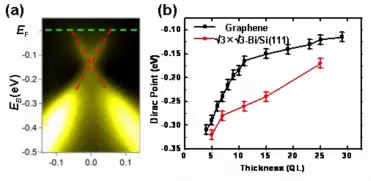
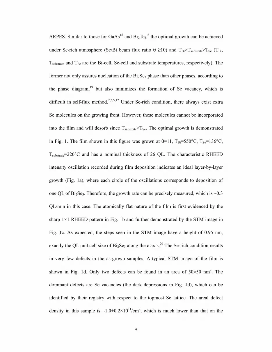
The electronic structure of the film is studied by ARPES and shown in Fig. 2a.
The Dirac cone (the dashed red lines) can be clearly seen, and the Dirac point is
located at 130 meV below EF. While the position of the Dirac point can change
(several tens meV) with film thickness, what’s important here is that the intense
electronic pocket from the bulk conduction band observed in the cleaved crystals2,3,12
does not appear, suggesting that the film at this thickness is already a bulk insulator.
Given the conditions we used, it is found that the minimum thickness for the film
being an “intrinsic” TI is 11 QL. The details of this result has been discussed
elsewhere.4
We also tried another substrate Si(111)-7×7. To avoid possible formation of SiSe2
and other selenides at the interface,21 the Bi-terminated √3×√3 structure was first
grown.20 In spite of it, the morphology of the Bi2Se3 films on the Bi-terminated √3×√3
surface, especially in the very thinner regime, is ill-defined. Moreover, the films suffer
from stronger electron-doping, which can be seen by a comparison of the ARPES data
on both substrates (Fig. 2b). Clearly, the Bi2Se3(111) films on graphene show much
quicker development to the bulk insulating state than those on the √3×√3-Bi/Si(111)
substrate, suggesting more defects and poorer film quality in the latter case. The
critical thickness for “intrinsic” TIs on the Bi-terminated Si(111) surface is as high as
24 QL.
Now we discuss the role of the double-layer graphene. In a heteroepitaxial
6
growth, the interface plays very critical roles in growth mode, strain relaxation and
formation of defects such as misfit and screw dislocations. The situation becomes
even more severe when a film is being deposited on a substrate of different material,
for example, Bi2Se3 on Si in which strong surface selenidization by Se molecules may
occur. By using inert graphene substrate, we found that not only is the interface
reaction completely suppressed, but also could the strain relaxation be complete at the
very first epitaxial layer of Bi2Se3, which doesn’t necessarily induce any dislocations
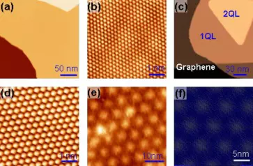
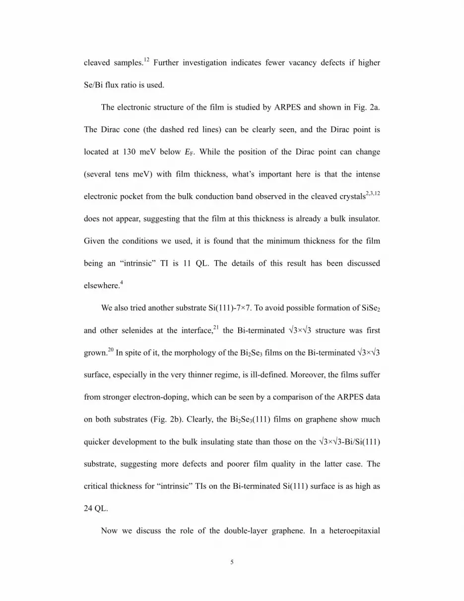
expected from the large lattice mismatch between graphene and Bi2Se3. Figures 3a
and 3b show the morphology and hexagonal atomic lattice of the graphene,
respectively, prepared on 6H-SiC(0001). After ~1.5 QL deposition, single crystalline
Bi2Se3 film is formed (Fig. 3c). At this stage, both 1 QL and 2 QL islands are
observed, implying an incomplete wetting of the graphene surface. From the
atomically resolved STM image of the 1 QL Bi2Se3 film in Fig. 3d, we know that
Bi2Se3(111)-1×1 surface is formed. The surface lattice constant measured with respect
to the exposed graphene is 0.41±0.01 nm, consistent with that (0.414 nm) of the bulk
Bi2Se3(111) surface. The observation reveals that the strain is already fully relaxed
even at the first QL. According to Figs. 3b and 3d, the close-packed direction of the
Se atoms is rotated by 28° with respect to that of the graphene. This leads to a
well-defined Morié pattern with a period of ~7.10 nm, as observed from dI/dV
mapping at -0.35 V (Fig. 3e). Assuming that the Bi2Se3(111) film is fully relaxed, a
simple simulation (Fig. 3f) indicates that, to form the Morié pattern in Fig. 3e, the
in-plane close-packed direction of the Bi2Se3(111) film should be rotated by 29°,
7
which is very close to the experimental value. It further supports a fully relaxed
Bi2Se3 film at 1 QL. Evidently, no interface reaction occurs and the Bi2Se3/graphene
interface is atomically sharp.
In summary, we have shown that graphene can serve a superb substrate for
growing high quality Bi2Se3 films. Under the growth criteria established in this study,
intrinsic TI films can be easily obtained when the thickness is above 10 QL. We
emphasize that the growth conditions presented here can be applied to growth of other
V-VI topological thin films and their heterostructures by standard MBE technique.
Acknowledgements: This work was supported by National Science Foundation and
Ministry of Science and Technology of China. XLQ and SCZ are supported by the
Department of Energy, Office of Basic Energy Sciences, Division of Materials
Sciences and Engineering, under contract DE-AC02-76SF00515. The STM
topographic images were processed by WSxM software (www.nanotec.es).
8
References
1 H. J. Zhang, C. X. Liu, X. L. Qi, X. Dai, Z. Fang, and S. C. Zhang, Nature Phys. 5, 438 (2009).
2 Y. Xia, D. Qian, D. Hsieh, L. Wray, A. Pal, H. Lin, A. Bansil, D. Grauer, Y. S. Hor, R. J. Cava,
and M. Z. Hasan, Nature Phys. 5, 398 (2009).
3 D. Hsieh, Y. Xia, D. Qian, L. Wray, J. H. Dil, F. Meier, J. Osterwalder, L. Patthey, J. G.
Checkelsky, N. P. Ong, A. V. Fedorov, H. Lin, A. Bansil, D. Grauer, Y. S. Cava, and M. Z.
Hasan, Nature (London) 460, 1101 (2009).
4 Y. Zhang, K. He, C. Z. Chang, C. L. Song, L. L. Wang, X. Chen, J. J. Jia, Z, Fang, X. Dai, W. Y.
Shan, S. Q. Shen, Q. Niu, X. L. Qi, S. C. Zhang, X. C. Ma, and Q. K. Xue, Nature Phys.
(DOI:10.1038/NPHYS1689, June 13, 2010).
5 Y. L. Chen, J. G. Analytis, J. H. Chu, Z. K. Liu, S. K. Mo, X. L. Qi, H. J. Zhang, D. H. Lu, X.
Dai, Z. Fang, S. C. Zhang, I. R. Fisher, Z. Hussain, and Z. X. Shen, Science 325, 178 (2009).
6 Y. Y. Li, G. Wang, X. G. Zhu, M. H. Liu, C. Ye, X. Chen, Y. Y. Wang, K. He, L. L.Wang, X. C.
Ma, H. J. Zhang, X. Dai, Z. Fang, X. C. Xie, Y. Liu, X. Q. Qi, J. F. jia, S. C. Zhang, and Q. K.
Xue, Arxiv: 0912.5054 (2009).
7 P. Roushan, J. Seo, C. V. Parker, Y. S. Hor, D. hsieh, D. Qian, A. Richardella, M. Z. Hasan, R. J.
Cava, and A. Yazdani, Nature (London) 460, 1106 (2009).
8 T. Zhang, P. Cheng, X. Chen, J. J. Jia, X. C. Ma, K. He, L. L. Wang, H. J. Zhang, X. Dai, Z.
Fang, X. C. Xie, and Q. K. Xue, Phys. Rev. Lett. 103, 266803 (2009).
9 X. L. Qi and S. C. Zhang, Phys. Today 63, 33 (2010).
10 J. E. Moore, Nature (London) 464, 194 (2010).
11 M. Z. Hasan and C. L. Kane, Arxiv:1002.3895 (2010).

9
12 Y. S. Hor, A. Richardella, P. Roushan, Y. Xia, J. G. Checkelsky, A. Yazdani, M. Z. Hasan, N. P.
Ong, and R. J. Cava, Phys. Rev. B 79, 195208 (2009).
13 S. Urazhdin, D. Bilc, S. H. Tessmer, and S. D. Mahanti, Phys. Rev. B 66, 161306(R) (2002).
14 S. Urazhdin, D. Bilc, S. D. Mahanti, and S. H. Tessmer, Phys. Rev. B 69, 085313 (2004).
15 A. K. Geim, and K. S. Novoselov, Nature Mater. 6, 183 (2007).
16 J. Hass, W. A. D. Heer, and E. H. Conrad, J. Phys.: Condens. Matter. 20, 323206 (2008).
17 X.-C. Ma, P. Jiang, Y. Qi, J.-F. Jia, Y. Yang, W.-H. Duan, W.-X. Li, X. Bao, S. B. Zhang, and
Q.-K. Xue, Proc. Natl. Acad. Sci. U.S.A. 104, 9204 (2007).
18 Q. K. Xue, T. Hashizume, and T. Sakurai, Prog. Surf. Sci. 56, 1 (1997).
19 H. Okamoto, and L. E. Tanner, Bi-Se (Bismuth-Selenium) Phase Diagram, ASM (1986).
20 G. H. Zhang, H. J. Qin, J. Teng, J. D. Guo, Q. L. Guo, X. Dai, Z, Fang, and K. H. Wu, Appl.
Phys. Lett. 95, 053114 (2009).
21 R. D. Bringans and M. A. Olmstead, Phys. Rev. B 39, 12985 (1989).

10
Figure captions
FIG. 1. (a) RHEED intensity of the (0, 0) diffraction versus growth time. (b) RHEED
pattern along Γ-K direction and (c) STM image of the 26 QL Bi2Se3 film acquired at a
sample bias (Vs) of 1.0V. (d) STM image (Vs=10 mV) showing the Se vacancies (the
blue arrows).
FIG. 2. (a) ARPES intensity map of the 26 QL film along the Γ-K direction. The green
dotted line indicates the Fermi level, and the red ones the topological surface states. (b)
thickness-dependent surface Dirac point of Bi2Se3 films on graphene (black curve)
and Si (red curve) substrates.
FIG. 3. (a) Large scale (Vs=4.0 V) and (b) atomic resolution STM images (Vs=10 meV)
of double-layer graphene on SiC(0001) substrate. (c) STM image (Vs=1.0V) recorded
after deposition of 1.5 QL Bi2Se3 on graphene. (d) High-resolution STM image (Vs=10
meV) of 1 QL Bi2Se3 film. The bright spot corresponds to a topmost surface Se atom.
(e) dI/dV mapping of 1 QL Bi2Se3 film at Vs=-0.35V, revealing a Moiré pattern with a
period of 7.10 nm. (f) Simulated Moiré pattern by assuming a fully relaxed Bi2Se3 on
graphene.