Embed Size (px)
Citation preview
4Synchronous Finite-StateMachine Designs
This chapter looks at a numberof practical designs using the techniques developed inChapters 1
to 3. It compares the conventional design of FSMs with the design proposed in the book. This
illustrates howmore effective the latter method is in developing a given design. The traditional
method of designing FSMs is common in a lot of textbooks on digital design. It makes use of
transition tables and can become cumbersome to use when dealing with designs having a large
number of inputs. Even for designs having few inputs, the method used in Chapters 1–3 is
quicker and easier to use.
Most designers involved in the development of FSMs make use of unused secondary state
assignments to help reduce the flip-flop input and output equations. This practice is investigated
with some interesting results.
The chapter covers a number of practical system designs. Some have simulation waveforms
showing theFSMdesignworking.TheVerilogHDLcode used to create the simulationswill not
be shown, as VerilogHDL code development is not covered until later on in the book. However,
the respectiveVerilog codes are available on theCDROMdisk that is includedwith this book, as
are the Verilog tools used to view the simulations.
Eight examples are discussed in this chapter, with each example introducing techniques that
help to solve the particular requirements in the design being investigated.
4.1 TRADITIONAL STATE DIAGRAM SYNTHESIS METHOD
Before continuing with the development of FSM systems based on the synthesization method
covered in Chapters 1–3, it is worth investigating the more popular traditional method of
synthesization used by many system designers. Then see what solutions are obtained by using
both methods. It should be possible to obtain the same results, or at least results that are of a
similar level of complexity (i.e. number of gates).
Consider the state diagram shown in Figure 4.1. This, being a four-state diagram, will
need two D-type flip-flops. Using the traditional synthesization method, begin by con-
structing a state table containing the present state (PS) values and the next state (NS)
FSM-based Digital Design using Verilog HDL Peter Minns and Ian Elliott# 2008 John Wiley & Sons, Ltd. ISBN: 978-0-470-06070-4

values for A and B, for all possible values of the input x. One then adds to this the next
states for the inputs Da and Db, for all possible values of x. The result is the state table
shown in Table 4.1.
The values for A and B in Table 4.1 are obtained by inspection of the state diagram in
Figure 4.1. For example, in state s0 (PS of AB ¼ 00) in col1 the NS of AB for x ¼ 0 will
be 00 in col2; however, if x ¼ 1, the NS of AB ¼ 01 in col3 (i.e. s1).
The values for the NS Da and Db values will follow the NS values for AB because in a
D flip flop the output of the flip flop (A, B) follows the Da and Db inputs.
The reader can follow the rest of the rows in Table 4.1 to complete the state table.
Table 4.1 Present state–next state table for the state machine.
col1 col2 col3 col4 col5
PS NS NS NS NS
AB AB AB DaDb DaDb
x ¼ 0 x ¼ 1 x ¼ 0 x ¼ 1
Row1 00 00 01 00 01
Row2 01 11 01 11 01
Row3 11 00 10 00 10
Row4 10 11 00 11 00
/Zs0
/Zs1
/Zs2
Zs3
x_| /x_|
/x_|
x_|/x_|
x_|
AB00
AB01
AB11
AB10
Figure 4.1 A state diagram used in the comparison.
68 Synchronous Finite-State Machine Designs
The next step is to obtain the Da and Db equations from the state table by writing
down the product terms where Da ¼ 1 in both columns x ¼ 0 and x ¼ 1.
Consider, for example, Da ¼ 1 when A changes 0 to 1; look for PS A ¼ 0 to NS A ¼ 1
in row 2, and PS A ¼ 1 to NS A ¼ 1 in row 3 of columns 1, 3 (x ¼ 1):
� when PS AB ¼ 01 (row 2) and x ¼ 0, flip-flop A should set, and the product term /AB/x is
required;
� whenPSAB ¼ 01 and x ¼ 1 (row2, col3), flip-flopA should be reset, and the term /ABx is not
required;
� when PS AB ¼ 10 (row 4) and x ¼ 0, flip-flop A should set, and the term A/B/x is
required;
� when PS AB ¼ 11 (row 3) and x ¼ 1, flip-flop A should be set, and term ABx is required.
Therefore, the D input terms for Da are
D�a ¼ =AB�=xþ A=B�=xþ AB�x;
which cannot be reduced. For D �b¼ /A/B �xþ /AB � /xþ /AB �xþ A/B � /x we have
D�b ¼ =A�xþ =ABþ A=B�=x:
The output equation for Z ¼ s3 ¼ A=B, since this is a Moore state machine.
Now do the problem using the synthesization method described in Chapters 1�3.
From the state diagram directly:
Da ¼ s1�=xþ s2� xþ s3�=x¼ =AB�=xþ AB�xþ A=B�=x
Db ¼ s0� xþ s1þ s3�=x¼ =A=B� xþ =ABþ A=B
¼ =A� xþ =ABþ A=B�=x:
This is the same as obtained using the traditional method.
Themain advantage of themethod used inChapters 1–3, over the traditionalmethod, is that it
does not require the use of the state table. It is also much easier to usewhen the number of input
variables is large (as is the case in largepracticalFSMdesigns) since the sizeof thepresent state–
next state table increases as more inputs are added.
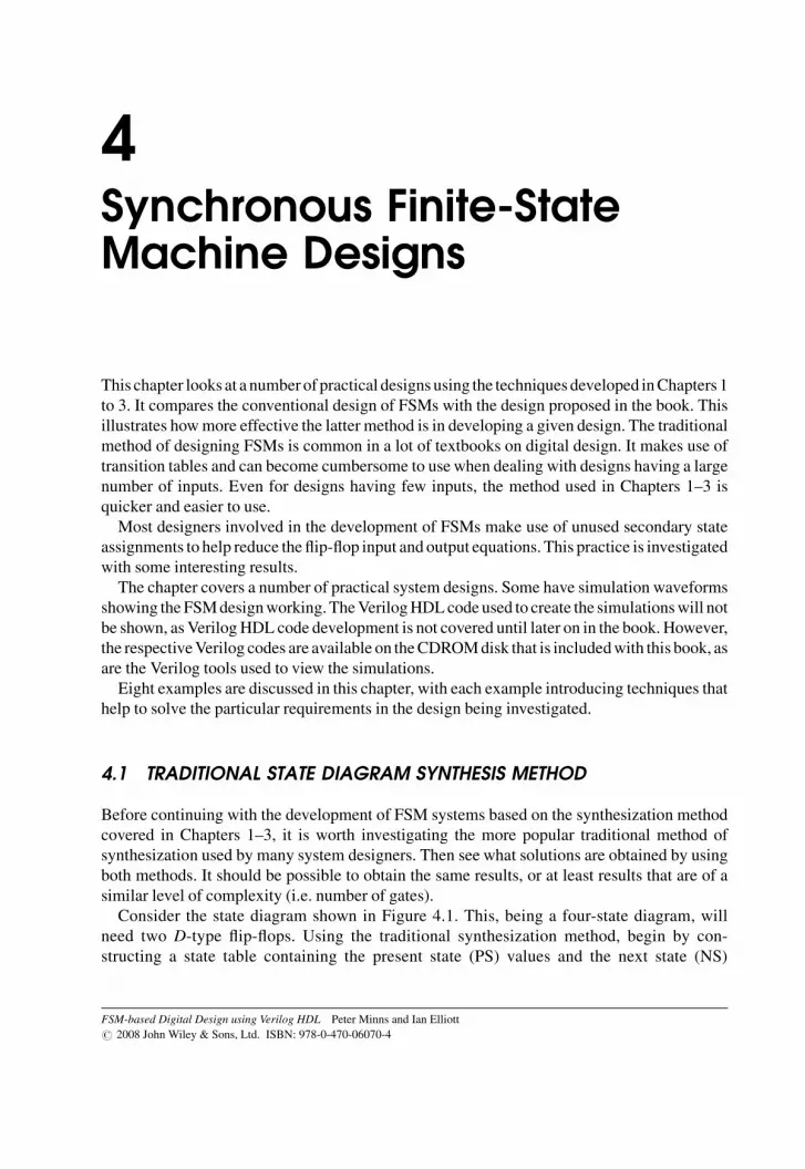
4.2 DEALING WITH UNUSED STATES
Whendeveloping statediagrams that use less than the2n states forn secondary statevariables the
question of what to do with the unused states arises. Consider the state diagram of Figure 4.2.
Dealing with Unused States 69
From the state assignment used in this example there are
Used states Unused states
s0¼ 000 s5¼ 010
s1¼ 100 s6¼ 110
s2¼ 101 s7¼ 001
s3¼ 111
s4¼ 011
The equations for D flip-flops are:
A � d ¼ s0 � sþ s1þ s2þ s3 � z¼ ���=A =B=C � sþ A=B���=C þ A=B���=C þ A���=BC � z:
The crossed-out literals are a result of applying logical adjacency and the aux rule (see
Appendix A). The result is
A � d ¼ =B=C � sþA=BþAC � zB �d ¼ s2 � yþ s3 � =zþ s4
¼ A=BC � yþ���=ABC � =zþ =ABC
¼ A=BC � yþBC � =zþ =ABC
C � d ¼ s1 � xþ s2 � yþ s3þ s4
¼ A=B=C � xþA���=B=C � yþ���=ABCþ���=ABC:
s0/P, /Q
s1P, /Q
s2P,Q
s3/P,Q
s4/P,/Q
ABC000
ABC100
ABC101
ABC111
ABC011
s_|x_|
/y_|
y_|
z_|
/z_|
Figure 4.2 A state diagram using less than the 23 states.
70 Synchronous Finite-State Machine Designs

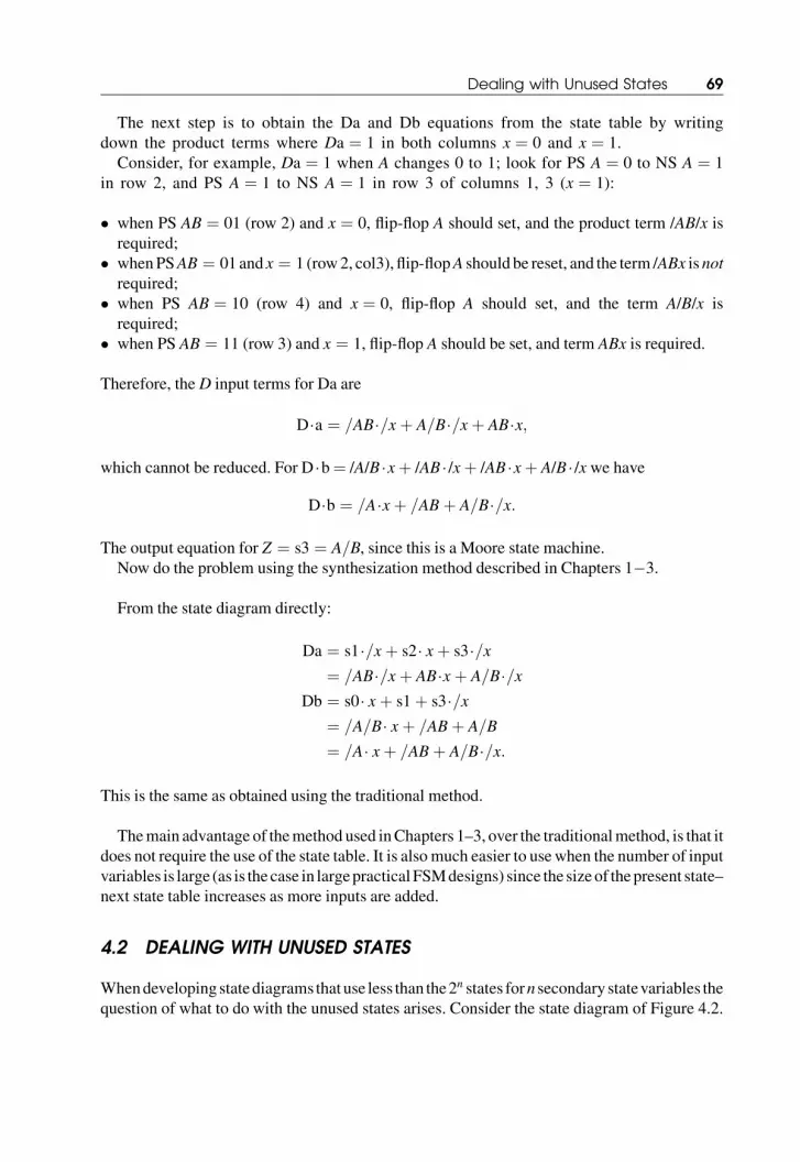
Again, the crossed-out terms are using logical adjacency and the aux rule.
C � d ¼ A=B=C � xþ AC � yþ BC:
The output equations:
P ¼ s1þ s2 ¼ A=B=C þ A=BC
P ¼ A=B
Q ¼ s2þ s3 ¼ A=BC þ ABC
Q ¼ A=BC þ ABC ¼ AC:
If the state machine falls into the unused state s5 (/AB/C) then the result will be
A � d ¼ 0;B � d ¼ 0; and C � d ¼ 0 the state machine falls into s0:
If the state machine falls into unused state s6 (AB/C):
A � d ¼ 0;B � d ¼ 0; andC � d ¼ 0 again; the state machine will fall into s0:
If state machine falls into the unused state s7 (/A/BC):
A � d ¼ 0;B � d ¼ 0; and C � d ¼ 0 with next state being s0 again:
This shows that the FSM designed with D-type flip-flops will be self- resetting.
Note that ifTflip-flops are used, then theFSMwill not be self-resetting since theT input either
toggles with T ¼ 1 or remains in its current statewith T ¼ 0. The only way to ensue that it does
return to s0 is to make transitions available for this, as illustrated in Figure 4.3. Clearly, this
requires more product terms in the equations for A � t, B � t, and C � t.In general, if the state machine has a lot of 1-to-1 transitions and few 1-to-0 and
0-to-1 transitions, then T flip-flops may need less terms and, hence, a possible deduction in
logic.
If the state machine has few 1-to-1 transitions the D flip-flop solution may result in fewer
terms. However, the self-resetting features of theD flip-flopmay provide a greater advantage in
the overall design.
The rest of this chapter contains anumberofpractical examples,makinguse of the techniques
developed in the first three chapters.
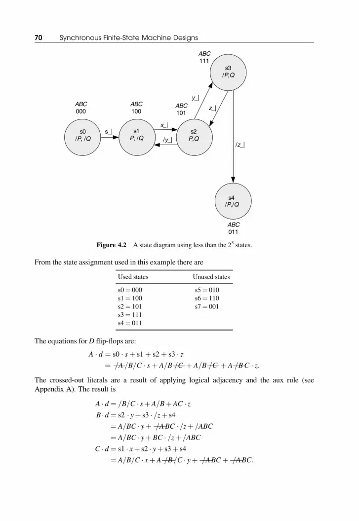
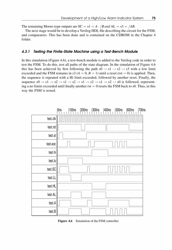
4.3 DEVELOPMENT OF A HIGH/LOW ALARM INDICATOR SYSTEM
Figure 4.4 illustrates a block diagram for the proposed system. In Figure 4.4, the FSM is used to
control anADCandmonitor the converted analogue signal levels until either the low-level limit
or the high-level limit is exceeded. The low- and high-level values are set up on the Lo-word/
Hi-word inputs, which could be dual in-line switches. The comparators are standard 8-bit
Development of a High/Low Alarm Indicator System 71
8
8
8
8
8
Hi-word
Lo-word
Vin
ADC
8-Bit Comparators
Synchronous FSM
iholcoeCS
AL
rst
Vcc
LL HL
LowLED
HighLED
CLKSystemReset
A B
A B
A>B
A<B
st
Figure 4.4 Block diagram for the High/Low detector system.
S0
/p, /q
S1
p, /qS2
P,q
S3
/p,q
S4/p,/q
ABC
000
ABC
100ABC
101
ABC
111
ABC
011
s0
/P, /Q
s1
P, /Qs2
P,Q
s3
/P,Q
s4/P,/Q
ABC
000
ABC
100ABC
101
ABC
111
ABC
011
s_|
x_|
/y_|
y_| z_|
/z_|
_|
_| _|
s5 s6 s7
ABC
010ABC
110
ABC
001
Figure 4.3 The arrangement needed for T flip-flops.
72 Synchronous Finite-State Machine Designs

comparator circuits similar to the standard7485devices.These couldeasilybe incorporated into
a PLD/FPGA along with the FSM.
In this application it is assumed that, when theADC outputA exceeds the Hi-word, hi will go
to logic 1. AnADCoutput less than the Lo-wordwill make lo go to logic 1. TheADC could be a
separate device or its digital circuits could be implemented on a PLD/FPGA device and an
external R/2R network connected to the chip.
Thesystemis to startwhenstgoeshigh. It shouldperformanalogue-to-digital conversionsat a
regular sampling frequency dictated by the system clock and when either the Hi-word or Lo-
wordare exceeded, turnon theappropriateLEDindicator andstop. It canbe returned to its initial
state by operation of the reset button. Note that in this example the alarm will not sound for an
ADC output that is equal either to Hi-word or Lo-word.
From this specification, a state diagramcanbe developed. The control of theADCwill follow
in much the same way that was used in Chapter 2.
The two digital comparators being combinational logic will give an output dependent on the
level of the ADC output.When the ADC output is equal to or less than hi-word but greater than
Lo-word, thenboth loandhiwill be low, signifying that theADCvalue isbetween the two limits.
When the ADC output is greater than Hi-word, then hi will be logic 1 and is to sound the alarm
and turnon theHLindicator.When theADCoutput is less thanLo-word, then lobecomes logic1
and the alarm turns on the LL indicator.
A state diagramhas been developed as shown in Figure 4.5. Looking at this state diagram, the
systemsits in s0 frompoweron reset andwaits for the start input togohigh.Then theADCsignal
SC is raised to perform an analogue-to-digital conversion. After this the system falls into s2.
Here, the outputs from the two comparators are checked, and if either the Hi-word or the Lo-
word limit has been exceeded then the state machine will fall into s3. If, however, neither limit
has been exceeded, then the statemachinewill fall back into s1 to perform another analogue-to-
digital conversion.
/SC,LL,HL,/ALs0
SCs1
/SCs2
AL/LL=lo/HL=hi
s3
st_| eoc_|
lo+hi_|
/(lo+hi) _|
In s3 /LL = lo is in fact LL = /(s3.lo)
In s3 /HL = hi which is HL = /(s3.hi)
Both are mealy outputs
Note: /(lo + hi) is the same as lo + hi
AB00
AB10
AB11
AB01
Figure 4.5 A possible state diagram for the problem.
Development of a High/Low Alarm Indicator System 73
Looking at the two-way branch state s2, it is clear that the inverseof loþ hi is /(loþ hi).As an
aside, if one applies DeMorgan’s rule to /(loþ hi) one gets /lo � /hi, indicating for the transitionfrom s2 to s1 that both lo and hi must be low.
Moving on to look at s3, one can see that the two outputs HL and LL are dictated by the logic
state of the comparator outputs lo and hi so that in s3 theHL indicator should be active if hi¼ 1,
whereas the LL indicator should be active if lo¼ 1.
/HL¼ hi in s3 indicates that HL must be active low. The output equation for HL will be
written as
HL ¼ =ðs3 � hiÞ;
whichmeans thatHLwill be logic0whenhi¼ 1, butonlywhen the statemachine is in s3.This is
defining a Mealy active low output. This is how it was defined in Chapter 3.
In a similar way, LL ¼ =ðs3 � loÞ:
The best way to remember this idea is to think of the /HL¼ hi equation in the s3 state as
representing the equation HL ¼ /ðs3 � hiÞ, but then written inside the state circle one does notneed to include the s3, as it is implied.
Replacing the state number s3with its secondary statevariablevalueAB ¼ 01, the twoMealy
outputs can be written as
HL ¼ =ðs3 � hiÞ ¼ =ð=A � B � hiÞ and LL ¼ =ðs3 � loÞ ¼ =ð=A � B � loÞ;
which results in two three-input NAND gates. Remember, active low signals are inverted
(see Chapter 3).
So, from the equation for HL ¼ =ð=A � B � hiÞ it can be seen that, when in state s3, A ¼ 0
ð=A ¼ 1Þ, B ¼ 1, and if hi¼ 1 then the output of the NAND gate will be zero, which is exactly
what is required to light the LED indicator (active low output).
Havinggone into somedetail to describe the logicbehind theMealyoutputs, thenext step is to
determine the equations for the two flip-flopsA andB.Using themethod described in Chapter 3
for D flip-flops, these are
A � d ¼ s0 � stþ s1þ s2 � =ðloþ hiÞ ¼ =A � =B � stþ A � =Bþ A � B � =hi � =lo:
The equation for A � d could be simplified using the Auxiliary rule to form
A � d ¼ =B � stþ A � =Bþ A � =lo � =hi:
Moving on to flip-flop B:
B � d ¼ s1 � eocþ s2 � ðloþ hiÞ þ s3: ¼ A � =B � eocþ A � B � loþ A � B � hiþ =A � B:
Again, using the Auxiliary rule:
B � d ¼ A � =B � eocþ B � loþ B � hiþ =A � B:
74 Synchronous Finite-State Machine Designs
The remaining Moore-type outputs are SC ¼ s1 ¼ A � =BandAL ¼ s3 ¼ =AB.The next stage would be to develop a Verilog HDL file describing the circuit for the FSM,
and comparators. This has been done and is contained on the CDROM in the Chapter 4
folder.
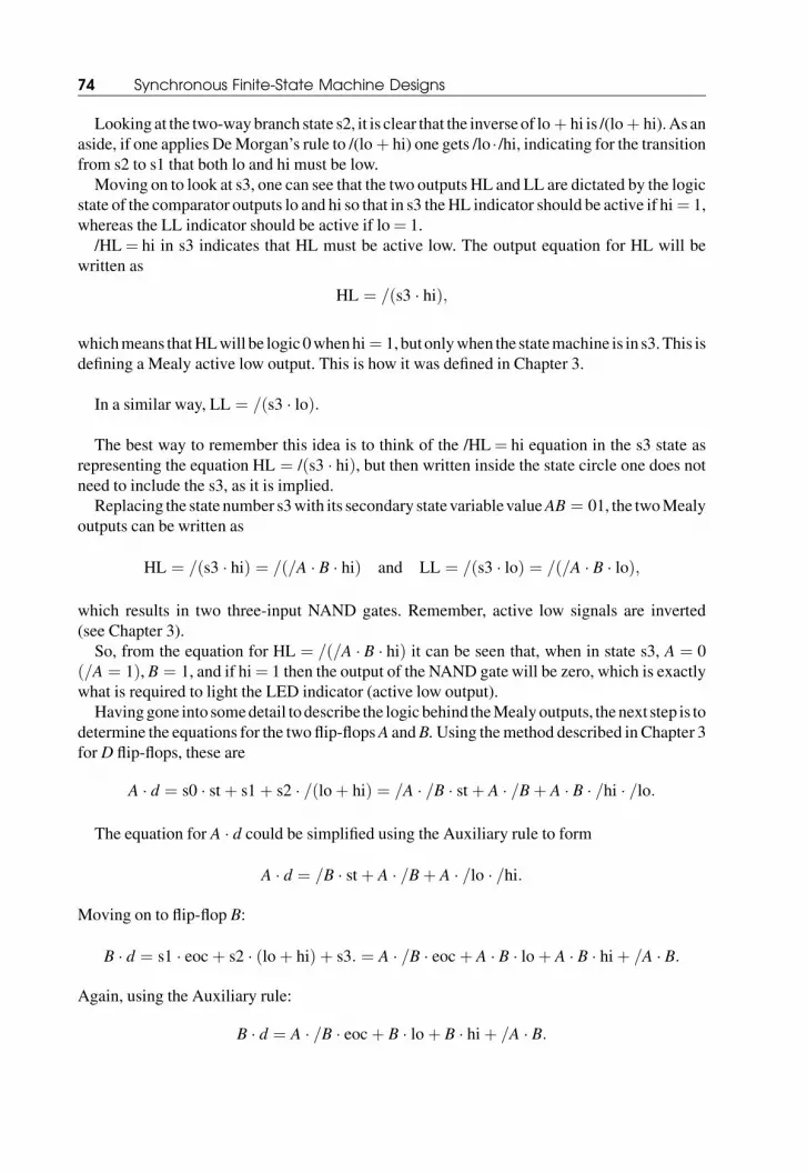
4.3.1 Testing the Finite-State Machine using a Test-Bench Module
In this simulation (Figure 4.6), a test-bench module is added to the Verilog code in order to
test the FSM. To do this, test all paths of the state diagram. In the simulation of Figure 4.6
this has been achieved by first following the path s0 ! s1 ! s2 ! s3 with a low limit
exceeded and the FSM remains in s3 (A ¼ 0, B ¼ 1) until a reset (rst ¼ 0) is applied. Then,
the sequence is repeated with a Hi limit exceeded, followed by another reset. Finally, the
sequence s0 ! s1 ! s2 ! s1 ! s2 ! s1 ! s2 ! s1 ! s2 ! s0 is followed, represent-
ing a no limits exceeded until finally another rst ¼ 0 resets the FSM back to s0. Thus, in this
way the FSM is tested.
0ns 100ns 200ns 300ns 400ns 500ns 600ns 700ns
test.clk
test.rst
test.st
test.eoc
test.hi
test.lo
test.SC
test.LL
test.HL
test.AL
test.A
test.B
Figure 4.6 Simulation of the FSM controller.
Development of a High/Low Alarm Indicator System 75
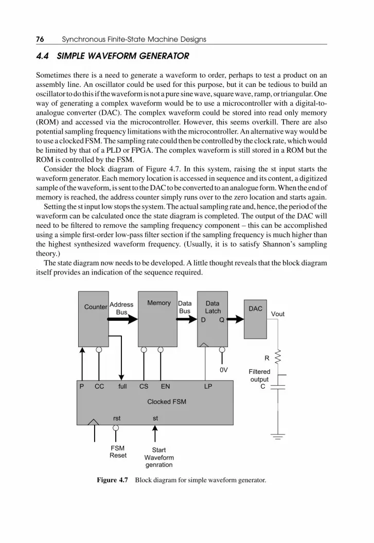
4.4 SIMPLE WAVEFORM GENERATOR
Sometimes there is a need to generate a waveform to order, perhaps to test a product on an
assembly line. An oscillator could be used for this purpose, but it can be tedious to build an
oscillator todo this if thewaveform isnot apure sinewave, squarewave, ramp, or triangular.One
way of generating a complex waveform would be to use a microcontroller with a digital-to-
analogue converter (DAC). The complex waveform could be stored into read only memory
(ROM) and accessed via the microcontroller. However, this seems overkill. There are also
potential sampling frequency limitationswith themicrocontroller.An alternativewaywould be
to use a clockedFSM.The sampling rate could thenbe controlled by the clock rate,whichwould
be limited by that of a PLD or FPGA. The complex waveform is still stored in a ROM but the
ROM is controlled by the FSM.
Consider the block diagram of Figure 4.7. In this system, raising the st input starts the
waveform generator. Eachmemory location is accessed in sequence and its content, a digitized
sample of thewaveform, is sent to theDACtobeconverted to ananalogue form.When the endof
memory is reached, the address counter simply runs over to the zero location and starts again.
Setting the st input lowstops the system.Theactual sampling rate and, hence, theperiodof the
waveform can be calculated once the state diagram is completed. The output of the DAC will
need to be filtered to remove the sampling frequency component – this can be accomplished
using a simple first-order low-pass filter section if the sampling frequency is much higher than
the highest synthesized waveform frequency. (Usually, it is to satisfy Shannon’s sampling
theory.)
The state diagram now needs to be developed. A little thought reveals that the block diagram
itself provides an indication of the sequence required.
R
C
DACData
Latch
MemoryCounter
Clocked FSM
Address
Bus
Data
Bus
D QVout
P CC full CS EN LP
rst st
FSMReset
Start
Waveformgenration
Filtered
output
0V
Figure 4.7 Block diagram for simple waveform generator.
76 Synchronous Finite-State Machine Designs
1. Initially, the address counter needs to be cleared to provide the necessary zero address for the
first location of the memory. The system should remain in state s0 until the start input st is
asserted (high).
2. Thememory then needs to be enabled, selected, and allowed to settle, after which the data in
thememory locationwill beavailable at thedata latch inputs.Then thedataneed tobe latched
into the data latch to be available at the input of the DAC.
3. At this stage, the address counter needs to be incremented so as to point to the next memory
location and the sequence in 2 repeated again as long as the start input is still asserted (high).
Note that, in this problem, the end of memory location is not an issue, since the address counter
can be allowed to overrun and start from location zero again. This does imply that thewaveform
information canbefitted into thememorydevice so that thewaveform is produced seamlessly. It
would be possible to add further logic to the system to ensure that this was always the case, but
this is not done in this example.
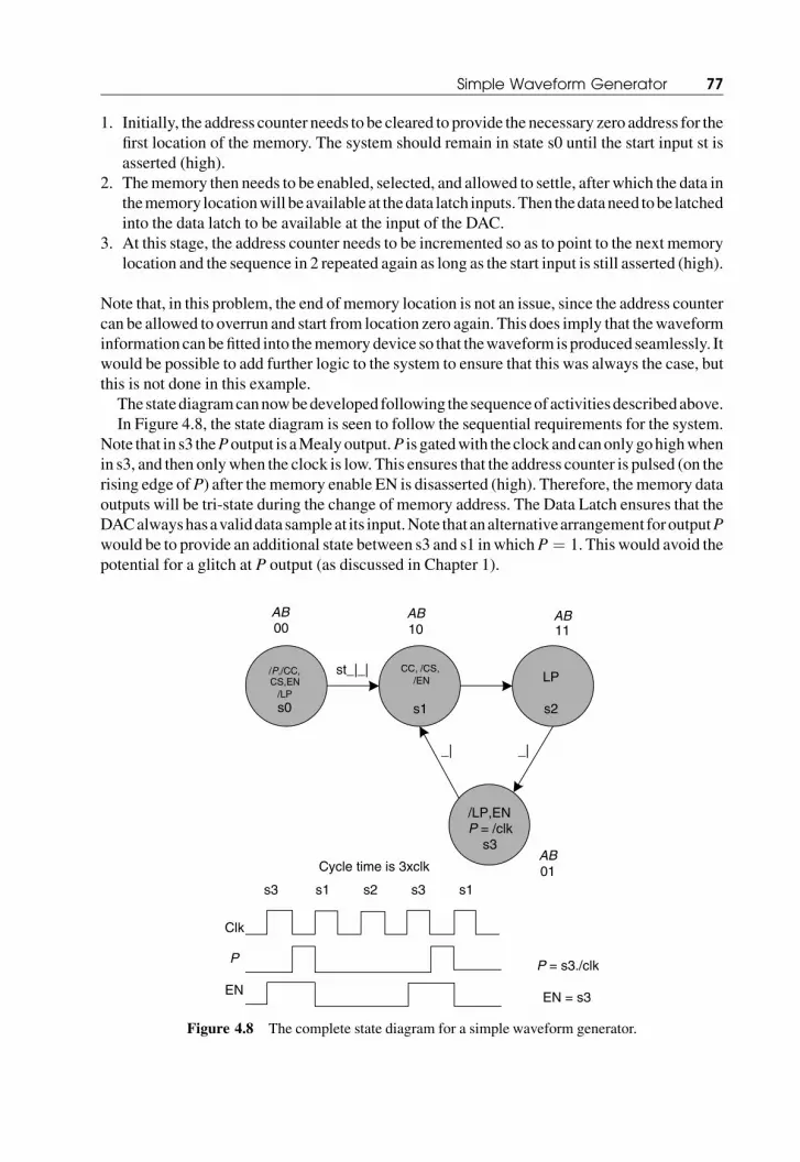
The statediagramcannowbedeveloped following the sequenceof activitiesdescribedabove.
In Figure 4.8, the state diagram is seen to follow the sequential requirements for the system.
Note that in s3 thePoutput is aMealyoutput.P is gatedwith the clockandcanonlygohighwhen
in s3, and then onlywhen the clock is low. This ensures that the address counter is pulsed (on the
rising edge ofP) after thememory enable EN is disasserted (high). Therefore, thememory data
outputs will be tri-state during the change of memory address. The Data Latch ensures that the
DACalwayshasavaliddata sampleat its input.Note that analternativearrangement foroutputP
would be to provide an additional state between s3 and s1 inwhichP ¼ 1. This would avoid the
potential for a glitch at P output (as discussed in Chapter 1).
Clk
P
EN
P = s3./clk
EN = s3
s3 s1 s2 s3 s1
/P,/CC,CS,EN
/LP
s0
CC, /CS, /EN
s1
LP
s2
/LP,ENP = /clk
s3
st_|_|
_|_|
AB00
AB10
AB11
AB01Cycle time is 3xclk
Figure 4.8 The complete state diagram for a simple waveform generator.
Simple Waveform Generator 77

The equations can now be developed:
A � d ¼ s0 � stþ s1þ s3
¼ =A � =B � stþ A � =Bþ =A � B¼ =B � stþ A � =Bþ =A � BB � d ¼ s1þ s2
¼ A � =Bþ A � B¼ A:
Outputs are
CC ¼ =s0 ¼ =ð=A � =BÞ an active low output:
CS ¼ s0 ¼ =A � =B although an active low signal it is only high in s 0:
LP ¼ s2 ¼ A � B:EN ¼ s0þ s3 ¼ =A high in these two states:
P ¼ s3 � =clk ¼ =A � B � =clk a Mealy output gated with the clock:
In Verilog, these equations can be entered directly, but using the Verilog convention for
logic:
AND is & OR is j NOT is � exclusive OR is :̂
These equations would be contained in an assign block thus:
assignA. d¼� B& st|A&�B|�A& B,B.d¼ A,CC¼� (� A & � B);CS¼� A& � B,LP¼ A&B,EN¼� A,P¼� A&B&� clk;
AppendixCcontains a tutorial onhowtoproduceaVerilogfile to simulate a statemachine.Also,
much more detail is available in Chapters 6 to 8.
4.4.1 Sampling Frequency and Samples per Waveform
From the state diagram of Figure 4.8 it is apparent that the system cycles though three states for
every memory access, so the sampling period is three times the clock period.
Therefore, for a sampling frequency of 300� 103 Hz, a clock of 300�103�3¼ 900�103 Hz
is required. For a critical sampling-rate application, a dummy state could be added to make the
sampling frequency four times the clock frequency (for example).
The size of the memory can be whatever is required for the systems use, and will dictate the
size of the address counter. If the memory is 1 Kbyte, the address counter needs to be
78 Synchronous Finite-State Machine Designs

Number of flip-flops in address counter ¼ lnð1024Þ=lnð2Þ ¼ 10:
The simulation of the FSM is illustrated in Figure 4.9.
4.5 THE DICE GAME
In this example the system consists of seven LED indicators, a p input, and a clock. The block
diagramof the system is shown inFigure 4.10,with a single push switchp.Theclock input could
be a simple oscillator circuit using a 555 timer chip running at 100 Hz so as to provide aflicker to
add effect.
The LED indicators are arranged as illustrated in Figure 4.11 to look more realistic. In this
design it is assumed that low-current LEDs are usedwith a forward current of 2 mA.Thismakes
the current-limiting resistors 1800� for a 5 Vsupply. It is also assumed that theFSMoutputs are
open drain. Figure 4.11 illustrates how the seven LED indicators would look for each number
displayed. The situation when all LEDs are off is not shown.
The state machine is simple to develop, as all that is required is to display each number in
sequence, but at a speed that the user cannot follow. The state diagram consists of seven states,
each one to display a given LED pattern. The transition between each state is conditional on the
input p being equal to one for each transition.When the user releases the p button the FSMwill
stop in a state. Because of the frequency of the clock, the user will not be able to follow the state
sequence, thus realizing the chance element of the game. Note that if the clock frequency is too
high then all the LED indicators will appear to be on when the p button is pressed. Having a
0ns 100ns 200ns 300ns
test.st
test.clk
test.rst
test.A
test.B
test.P
test.CC
test.CS
test.EN
test.LP
Figure 4.9 Simulation results for the FSM of the waveform synthesizer.
The Dice Game 79

L1
L3
L5
L2
L4
L6
L7
Dice format and possible LED patterns
LED2LED1
LED3 LED4
LED6LED5
LED7
Figure 4.11 Dice format for numbers.
Vdd = 5 V
FSM
L1
L2
L3
L4
L5
L6
p
100 HzClock
LED1
LED2
LED3
LED4
LED5
LED6
Block Diagram of Dice Game
LED7L7
Figure 4.10 Block diagram of the dice game FSM
80 Synchronous Finite-State Machine Designs
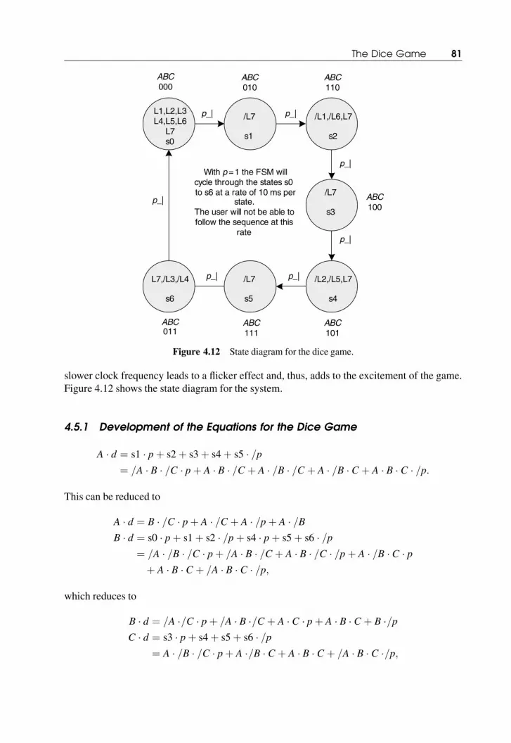
slower clock frequency leads to a flicker effect and, thus, adds to the excitement of the game.
Figure 4.12 shows the state diagram for the system.
4.5.1 Development of the Equations for the Dice Game
A � d ¼ s1 � pþ s2þ s3þ s4þ s5 � =p¼ =A � B � =C � pþ A � B � =C þ A � =B � =C þ A � =B � C þ A � B � C � =p:
This can be reduced to
A � d ¼ B � =C � pþ A � =C þ A � =pþ A � =BB � d ¼ s0 � pþ s1þ s2 � =pþ s4 � pþ s5þ s6 � =p
¼ =A � =B � =C � pþ =A � B � =C þ A � B � =C � =pþ A � =B � C � pþ A � B � C þ =A � B � C � =p;
which reduces to
B � d ¼ =A �=C � pþ =A � B �=C þ A � C � pþ A � B � C þ B �=pC � d ¼ s3 � pþ s4þ s5þ s6 � =p
¼ A � =B � =C � pþ A �=B � C þ A � B � C þ =A � B � C �=p;
L1,L2,L3L4,L5,L6
L7s0
/L7
s1
/L1,/L6,L7
s2
/L7
s3
/L2,/L5,L7
s4
/L7
s5
L7,/L3,/L4
s6
p_| p_|
p_|
p_|
p_|p_|
p_|
ABC000
ABC010
ABC110
ABC100
ABC101
ABC111
ABC011
With p = 1 the FSM willcycle through the states s0to s6 at a rate of 10 ms per
state.The user will not be able tofollow the sequence at this
rate
Figure 4.12 State diagram for the dice game.
The Dice Game 81

reducing to
C � d ¼ A � =B � pþ B � C � =pþ A � C:
The outputs (LEDs are active low) are
L1 ¼ ðs0þ s1Þ¼ð=A � =B �=Cþ=A � B �=C ¼ =A �=CÞ using active high in s0 and s1only:
L2 ¼ ðs0þ s1þ s2þ s3Þ ¼ =C using active high in these states only:
L3 ¼ =s6ðactive lowÞ ¼ =ð=A � B � CÞ:L4 ¼ =s6 ¼ =ð=A � B � CÞ low in s6 only; hence invert:
L5 ¼ =ðs4þ s5þ s6Þ ¼ =ðA � C þ B � CÞ low in only these states; hence invert:
L6 ¼ =ðs2þ s3þ s4þ s5þ s6Þ or ðs0þ s1Þ only high in s0 or s1 giving ð=A � =CÞ:L7 ¼ =ðs1þ s3þ s5Þ ¼ =ð=A � B � =C þ A � =B � =C þ A � B � CÞ:
Figure 4.13 illustrates thediceFSMrunning through each state.The secondary statevariables
a, b, and c can be seen to be moving through each state. The outputs L1 to L7 are responding as
expected and are illustrated in Figure 4.11.
0ns 50ns 100ns 150ns 200ns
test.p
test.clk
test.rst
test.a
test.b
test.c
test.L1
test.L2
test.L3
test.L4
test.L5
test.L6
test.L7
Figure 4.13 Simulation of the dice game.
82 Synchronous Finite-State Machine Designs

In Figure 4.14, the input p has been simulated as ‘on’ then ‘off’. The FSM is seen to have
stopped in state s3, then started again when p is set to logic 1.
Note that in both simulations the time-scale is in nanoseconds, but in practice the clockwould
be slowed down to a 10 ms period.
4.6 BINARY DATA SERIAL TRANSMITTER
The next example involves sending the 4-bit binary codes of a counter to a shift register to be
serially shifted out over a serial transmission line.
Figure 4.15 shows the block diagram for a possible system. The FSM is used to control the
operation of the Binary Counter and the Parallel Loading Shift Register. Both of these devices
could be designed using the techniques described in Appendix B on counting methods. This
leads to a Verilog description (module) for each device.
The system is started by raising the st input to logic 1. This is to cause the FSM to remove
the reset from the Binary Counter and then load the current count value of the counter into
the parallel inputs of the shift register. On releasing the parallel load input LD to logic 1, the
shift register will clock the count value out over its transmit output (TX) at the baud rate
dictated by the clock. When the shift register is empty its RE signal will go high and this
0ns 50ns 100ns 150ns 200ns 250ns 300ns
test.p
test.clk
test.rst
test.L1
test.L2
test.L3
test.L4
test.L5
test.L6
test.L7
test.A
test.B
test.C
Figure 4.14 Dice game simulation with p input released showing FSM stopped in s3.
Binary Data Serial Transmitter 83

will be seen by the FSM, which will then determine whether the last count value has been
sent. This is seen by the FSM when done = 1, detected by the detector block (an AND gate).
If not the last counter value, then the next count value will be loaded into the shift register
and the sequence repeated until all count values have been sent. At this point the system
will stop and wait for st to be returned to its inactive state before returning the FSM to its
s0 state.
From the above description, the state diagram in Figure 4.16 is developed. This state
diagram is correct, but it is difficult to obtain a unit distance code for the secondary state
variables. If a dummy state s7 is added, then a unit distance coding between s6 and s0 can
be obtained for the secondary state variables A, B, and C. Note: it is not apparent from
Figure 4.17, but the outputs in state s7 are the same as the state it is going to (s0), apart
from the RC output. The s5 to s1 transition is not unit distance. If glitches are produced in
any outputs, then dummy states could be introduced between s5 and s1 to establish unit
distance coding. The reader might like to try to establish a unit distance code for the state
diagram. This would require introducing an additional state variable (flip-flop), since all 23
states have been used in this design.
Using Figure 4.17, the equations for the FSM are obtained from the state diagram and
implemented using D flip-flops:
A � d ¼ s1þ s2þ s3þ s4
¼ =A � B �=C þ A � B�=C þ A �=B �=C þ A �=B � C;
Binary Counter
Parallel Loading ShiftRegister (includes Re
counter)
P0 P1 P2 P3
TX
Ld
FSM
CB RC
rst
st
reLD
done
Reset counter
Clock Counterq0 q1 q2 q3
reset
RE
Register empty flag
Det
Load
Clk
Figure 4.15 Block diagram of the binary data serial transmitter.
84 Synchronous Finite-State Machine Designs

/RC
s0
RC
s1
/LD
s2
LD,CBs3
/CB
s4s5s6
st_| _|
_|
_|
re_|done_|
/st_|
ABC000
ABC010
ABC110
ABC100
ABC101
ABC111
ABC011
Remove resetfrom binary counter
Load parallelshift register
Pulse binarycounter
Wait for shiftregister to empty
Test for end ofbinary count sequence
/done_|
Wait for st going lowto return to s0.
Figure 4.16 State diagram for the binary data serial transmitter.
/RC
s0
RC
s1
/LD
s2
LD,CBs3
/CB
s4s5s6
st_| _|
_|
_|
re_|done_|
/st_|
ABC000
ABC010
ABC110
ABC100
ABC101
ABC111
ABC011
Remove resetfrom binary counter
Load parallelshift register
Pulse binarycounter
Wait for shiftregister to empty
Test for end ofbinary count sequence
/done_|
Wait for st going lowto return to s0.
_|
s7
ABC001
Figure 4.17 State diagramwith additional dummystate s7 to obtain unit distance code for the secondary
state variables.
Binary Data Serial Transmitter 85

reducing to
A � d ¼ B �=C þ A �=BB � d ¼ s0 � stþ s1þ s4 � reþ s5þ s6 � st
¼ =A �=B �=C � stþ=A � B � =C þ A � =B � C � reþ A � B � C þ =A � B � C � st;
reducing to
B � d ¼ =A �=C � st þ =A � B �=C þ A � C � reþ B � C � stþ A � B � CC � d¼s3þ s4þs5 � doneþ s6 ¼ A � =B �=C þ A � =B � CþA � B � C � doneþ=A � B � C;
reducing to
C � d ¼ A � =Bþ B � C � doneþ =A � B � C:The outputs (all Moore) are
RC ¼ =s0ðactive lowÞ ¼ =ð=A � =B � =CÞLD ¼ =ðs2Þ ¼ =ðAB=CÞCB ¼ s3ðactive highÞ ¼ A � =B � =C:
The serial transmitter simulation is shown in Figure 4.18. The state machine is tracked
through its state sequence in the usual way by comparing the A, B, and C values in Figure 4.18
with the state diagram A, B, and C values in Figure 4.17.
0ns 100ns 200ns 300ns 400ns
test.st
test.clk
test.rst
test.re
test.done
test.A
test.B
test.C
test.RC
test.LD
test.CB
Figure 4.18 Simulation of the binary data serial transmitter.
86 Synchronous Finite-State Machine Designs

4.6.1 The RE Counter Block in the Shift Register of Figure 4.15
The shift register in Figure 4.15 has an output RE to flag the point at which the register is empty.
This can easily beobtainedbyusing a four-stageBinaryCounter that becomesenabledwhen the
load input is disasserted (high). The counter can then be clockedwith the same clock as the shift
register; then,when it reaches itsmaximumcount 1000, themost significant bit is used as theRE
signal. Table 4.2 illustrates the effect.
FromTable 4.2 it can be seen thatwhen the counter reaches the eighth clock pulse the counter
rolls over to set themost significant bit of the counterD to logic 1. This bit acts as theRE register
empty bit. After shifting out the binary number, the FSMwill return to its s0 state, where theRC
output will once again go low and reset both the Binary Counter and the RE counter in the shift
register. Note that in this particular design an additional flip-flopE could be added to the binary
counter and this used as the RE output instead
The equations to describe the RE counter can be developed from thematerial in Appendix B
on counting applications. The equations, using T-type flip-flops, are
A � t ¼ 1
B � t ¼ A
C � t ¼ A � BD � t ¼ A � B � CRE ¼ D:
This last example has illustrated how a complete design can be developed in terms of Boolean
equations that can be directly implemented in Verilog HDL (or any other HDL for that matter).
There are examples in Appendix B showing how a synchronous binary counter can be
implemented using T flip-flops. Of course, the counter could be implemented as an asynchro-
nous (ripple-through) counter if desired.
Table 4.2 Illustrating the effect of a binary counter used to determine shift register empty.
Binary counter
RE
D C B A Count value
0 0 0 0 0
0 0 0 1 1
0 0 1 0 2
0 0 1 1 3
0 1 0 0 4
0 1 0 1 5
0 1 1 0 6
0 1 1 1 7
1 0 0 0 8 Shift register empty when D ¼ 1
1 0 0 1 9 D output stays set
Binary Data Serial Transmitter 87
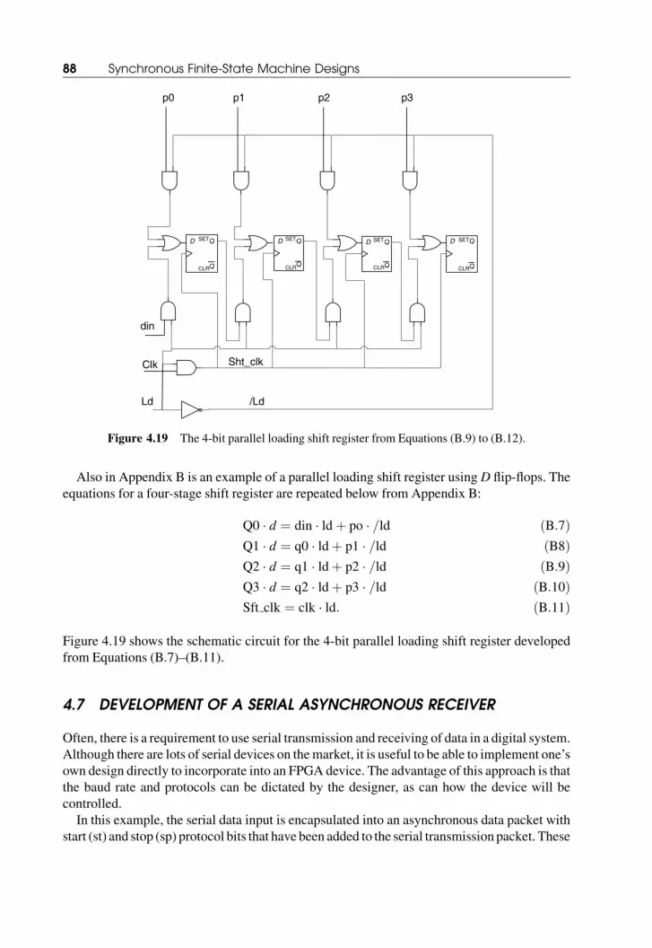
Also in Appendix B is an example of a parallel loading shift register using D flip-flops. The
equations for a four-stage shift register are repeated below from Appendix B:
Q0 � d ¼ din � ldþ po � =ld ðB:7ÞQ1 � d ¼ q0 � ldþ p1 � =ld ðB8ÞQ2 � d ¼ q1 � ldþ p2 � =ld ðB:9ÞQ3 � d ¼ q2 � ldþ p3 � =ld ðB:10ÞSft clk ¼ clk � ld: ðB:11Þ
Figure 4.19 shows the schematic circuit for the 4-bit parallel loading shift register developed
from Equations (B.7)–(B.11).
4.7 DEVELOPMENT OF A SERIAL ASYNCHRONOUS RECEIVER
Often, there is a requirement to use serial transmission and receiving of data in a digital system.
Although there are lots of serial devices on themarket, it is useful to be able to implement one’s
own design directly to incorporate into an FPGA device. The advantage of this approach is that
the baud rate and protocols can be dictated by the designer, as can how the device will be
controlled.
In this example, the serial data input is encapsulated into an asynchronous data packet with
start (st) and stop (sp) protocol bits that have been added to the serial transmission packet. These
Q
QSET
CLR
D
Q
QSET
CLR
D
Q
QSET
CLR
D
Q
QSET
CLR
D
Clk
Ld
din
p0 p1 p2 p3
/Ld
Sht_clk
Figure 4.19 The 4-bit parallel loading shift register from Equations (B.9) to (B.12).
88 Synchronous Finite-State Machine Designs
are used to provide a means of identifying the data packets as they arrive. This allows the data
packets to arrive at any time and at any selected rate (dictated by the baud rate).
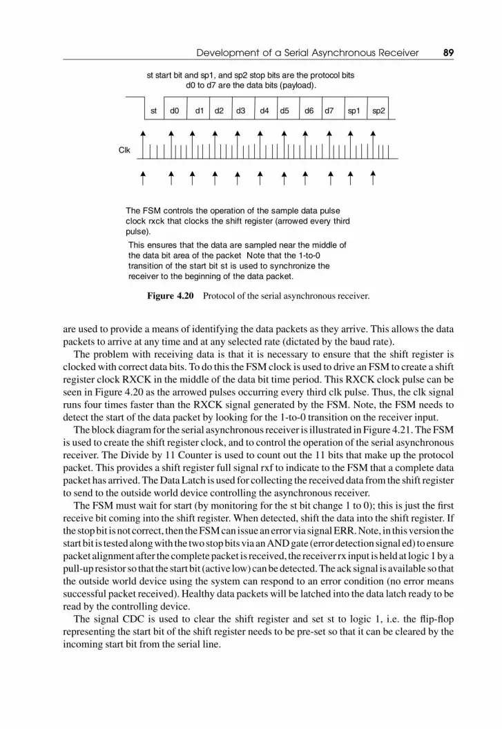
The problem with receiving data is that it is necessary to ensure that the shift register is
clocked with correct data bits. To do this the FSM clock is used to drive an FSM to create a shift
register clock RXCK in the middle of the data bit time period. This RXCK clock pulse can be
seen in Figure 4.20 as the arrowed pulses occurring every third clk pulse. Thus, the clk signal
runs four times faster than the RXCK signal generated by the FSM. Note, the FSM needs to
detect the start of the data packet by looking for the 1-to-0 transition on the receiver input.
The block diagram for the serial asynchronous receiver is illustrated in Figure 4.21. The FSM
is used to create the shift register clock, and to control the operation of the serial asynchronous
receiver. The Divide by 11 Counter is used to count out the 11 bits that make up the protocol
packet. This provides a shift register full signal rxf to indicate to the FSM that a complete data
packet has arrived. TheData Latch is used for collecting the received data from the shift register
to send to the outside world device controlling the asynchronous receiver.
The FSM must wait for start (by monitoring for the st bit change 1 to 0); this is just the first
receive bit coming into the shift register. When detected, shift the data into the shift register. If
the stopbit isnot correct, then theFSMcan issueanerrorvia signalERR.Note, in thisversion the
start bit is testedalongwith the twostopbits via anANDgate (error detection signal ed) toensure
packet alignment after the completepacket is received, the receiver rx input is held at logic1bya
pull-up resistor so that the start bit (active low)canbedetected.The ack signal is available so that
the outside world device using the system can respond to an error condition (no error means
successful packet received). Healthy data packets will be latched into the data latch ready to be
read by the controlling device.
The signal CDC is used to clear the shift register and set st to logic 1, i.e. the flip-flop
representing the start bit of the shift register needs to be pre-set so that it can be cleared by the
incoming start bit from the serial line.
Clk
st d0 d1 d2 d3 d4 d5 d6 d7 sp1 sp2
The FSM controls the operation of the sample data pulseclock rxck that clocks the shift register (arrowed every thirdpulse).
This ensures that the data are sampled near the middle ofthe data bit area of the packet Note that the 1-to-0transition of the start bit st is used to synchronize thereceiver to the beginning of the data packet.
st start bit and sp1, and sp2 stop bits are the protocol bitsd0 to d7 are the data bits (payload).
Figure 4.20 Protocol of the serial asynchronous receiver.
Development of a Serial Asynchronous Receiver 89

The en signal is used to enable and start the asynchronous receiver. This is necessary to ensure
that the system startsmonitoring the clock so as to issue the shift register clock pulse (RXCK) at
the right time (in the middle of the data bit period).
Figure 4.22 illustrates the state diagram for the system. In Figure 4.22, the FSMwaits for the
enable signal en going high and start signal st going low; it thenmoves through states s1, s2, and
s4 andonto s5 to shift the start bit into the shift register. This is required in order to ensure that the
start bit is detected and then shifted at the right time. In state s5, the shift register clockRXCK is
pulsed toplace the start bit into the shift register. It then falls into state s6, sendingRXCKlowand
proceeds to cycle through the second loop consisting of states s5, s6, s7, and s8.
These states count out the clock cycles and produce a shift register clock pulse (RXCK) at the
right time near the middle of each data bit. After all 11 bits have been clocked into the shift
register the 11-bit counter will issue a receive register full signal rxf, and the FSMwill now fall
into state s9,where thestart andstopbits are tested (edshouldbe logic1). If ed ¼ 0, then theFSM
will move into s10 and issue the error signal.
The controlling device can then reset the asynchronous receiver and start again. If no error,
then the FSMmoves to s11 to latch the data in the shift register into the data latch ready for the
controlling device to read (OQ0 to OQ7). It will also issue a data ready signal (DRY) to the
controlling device, which will acknowledge this by raising an ack signal. The FSM can then
move back to s0 via s12 (when ack goes low) towait for the next data packet. The DRYand ack
signals form a handshake mechanism between the FSM and the controlling device.
Data Latch
Shift Register
FSM
Divide
By 11
counter
QST Q0 Q1 Q2 Q3 Q4 Q5 Q6 Q7 QSP1 QSP2
PD
clk
st CDC rxf rxo RXCK
ed
DRY ERR ack en rst
Parallel data out – to outside world
Receivedata in
Error detectiondetection
Receive bit
Receive Shift
Register clockReceive
Register full
Clear Shift Register & counter
Start bitdetectionPulse
Data latch
DataReady
Error in
Receiveddata
Acknowledgeerror
Enable Device initialise system (controlled by outside
world device to recover from error)
rx
OQ0 OQ1 OQ2 OQ3 OQ4 OQ5 OQ6 OQ7
R
d0 d1 d2 d3 d4 d5 d6 d7
Vcc
clr
clr
Figure 4.21 Block diagram of the serial asynchronous receiver.
90 Synchronous Finite-State Machine Designs

The device enable signal en will be left high until all data packets have been received.
Note that the state assignments miss s3, which was removed from the state diagram during
development when state s3 was no longer needed (owing to an error in the design at that time).
State diagram development tends to be an iterative process.
4.7.1 Finite-State Machine Equations
A � d ¼ s0 � en � =stþ s1þ s2þ s4þ s5þ s8
B � d ¼ s1þ s2þ s4þ s5 � rxf þ s7þ s8þ s9þ s10þ s11 � =ackC � d ¼ s2þ s4þ s5 � =rxf þ s6þ s7þ s8þ s9 � edþ s11þ s12 � ackD � d ¼ s4þ s5þ s6þ s7þ s8þ s9 � =edþ s10
RXCK ¼ s5 ¼ ABCD
PD ¼ dry ¼ s11 ¼ =ABC=D
ERR ¼ s10 ¼ =AB=CD:
The reader may like to complete these to form the equations in terms of A, B, C, and D.
The complete asynchronous serial receiver block is simulated, together with all the modules
in Figure 4.21, in Appendix B.
/RXCK
s0 s2s1 s4
RXCK
s5s6s7s8
s9
ERR
s10
PD,DRY
s11
/PD,/DRY
s12
_|2en./st_|1 _|3
_|4
/rxf_|1_|2_|3
_|4
rxf_|
ed_|
/ed_|
ack_|
/ack_|
ABCD
0000
ABCD
1000
ABCD
1100
ABCD
1111
ABCD
1110
ABCD
1011
ABCD
0011
ABCD
0111
ABCD
1101
ABCD
0101
ABCD
0110
ABCD
0010
Wait for
enable
Test for
shift reg
full.2nd clk
received3rd clk
received
Shift reg. full
So check stop
Bits true
Start/Stop
bit error
No start/stop bit errors
so transfer data
from shift reg.
to data latch
and send data
Ready (DRY) to
controlling device
ack from controlling
device so return to state s0
for next data packet
Note: so initial signals are
/CDC, /PD, /ERR, /RXCK,/DRY
Pulse data
into shift reg.
Wait for st 1 to 0 transtition then
clock into shift register
/RXCK
RXCK
Figure 4.22 State diagrams for the serial asynchronous receiver.
Development of a Serial Asynchronous Receiver 91
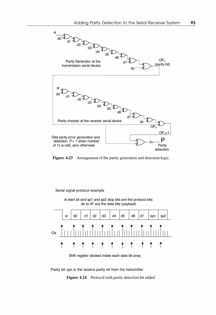
4.8 ADDING PARITY DETECTION TO THE SERIAL RECEIVER SYSTEM
The foregoing example could be improved upon bymaking the first stop bit sp1 into a parity bit.
The parity bit would require combinational logic to check each bit of the protocol packet for
either evenparity or odd parity. Thiswould require an exclusiveORblockmade upof the 11 bits
of the packet.
For example, odd parity would require an odd parity output OP at the Transmitter of
OP ¼ bo^b1^b2^b3^b4^b5^b6^b7^b8^b9^b10:
Or, including the protocol bits:
OPnþ1 ¼ st^d0^d1^d2^d3^d4^d5^d6^d7^OPn ^sp:
Thisoutputwouldbe testedby theFSMfor logic1. If logic0, thiswould indicate thatoneormore
of the received bits was faulty.
Note that even parity EP can be detected by complementing the OP signal:
EPn ¼ =OPn:
To implement the parity detector term, two input exclusive OR gates are cascaded with the last
exclusive OR gate providing the OPn signal. The output of the parity block at the receiver is P.
The inputsd0,d1; . . . ; d7will beobtained from theoutputof the shift register in eachcase (see
Figure 4.21).
4.8.1 To Incorporate the Parity
The parity detector inputs are connected to the outputs of the shift register and its output OPnmade available as an input to the FSMvia the last two bit comparator comparingOPn andOPnþ1
in Figure 4.23.
Figure 4.24 shows the new protocol with the parity bit OPn (shown in lower case)
replacing sp1.
Figure4.25 shows theadditionalparityblockadded to theblockdiagram.Thisversiondetects
stop and parity bit errors at the output of the shift register; the start bit has not been tested (but
could be included if desired).
Figure 4.26 illustrates the modified state diagram with ODD parity detection. Note that
the input parity bit OPnþ1 must be compared with the generated parity bit OPn. If both
are the same, then there is no parity error. This comparison can be made with a 2-bit
exclusive NOR gate having an output P (OPn ¼¼ OPnþ1) being logic 1 if there is no
parity error and logic 0 otherwise. This output is an input p to the state machine (see
Figure 4.25).
In state s9, the bit sp is checked to find out whether the whole packet has been input, and s11
nowtests for anoddparity error. In either casea failurewill result in theFSMaborting the receive
packet process and falling into state s10 to await a reset from the controlling device. The logic
used in Figure 4.21 could be used to detect for start and stop bits if desired.
92 Synchronous Finite-State Machine Designs
st
d0d1
d2d3
d4d5
d6d7
sp
OPn(parity bit)
Parity Generator at thetransmission serial device.
st
d0d1
d2d3
d4d5
d6d7
OPn
sp
OPn+1
Parity checker at the receiver serial device
Odd parity error generation and detection P = 1 when number of 1s is odd, zero otherwise Parity
detection
P
Figure 4.23 Arrangement of the parity generation and detection logic.
Parity bit opn is the receive parity bit from the transmitter
Clk
st d0 d1 d2 d3 d4 d5 d6 d7 opn sp2
Serial signal protocol example
st start bit and sp1 and sp2 stop bits are the protocol bitsdo to d7 are the data bits (payload)
Shift register clocked inside each data bit area
Figure 4.24 Protocol with parity detection bit added.
Adding Parity Detection to the Serial Receiver System 93

4.8.2 D-Type Equations for Figure 4.26
In the following equations, the variable P is the output of the parity check (OPn = OPnþ1)
connected to the input p of the FSM. See Figure 4.23.
A � d ¼ s0 � en � =stþ s1þ s2þ s4þ s5þ s8þ s9� sp¼ =A=B=C=D � en � =stþ A=B=C=Dþ AB=C=Dþ ABC=Dþ ABCD
þ=ABCDþ AB=CD � spB � d ¼ s1þ s2þ s4þ s5 � rxf þ s7þ s8þ s9 � =spþ s10þ s11þ s12 � =ack
¼ A=B=C=Dþ AB=C=Dþ ABC=Dþ ABCD � rxf þ =A=BCD þ =ABCD
þAB=CD � =spþ =AB=CDþ A=B=CDþ =ABC=D � =ackC � d ¼ s2þ s4þ s5 � =rxf þ s6þ s7þ s8þ s11 � pþ s12þ s13 � ack
¼ AB=C=Dþ ABC=Dþ ABCD � =rxf þ A=BCDþ =A=BCDþ =ABCD
þ A=B=CD � pþ =ABC=Dþ =A � =B � C � =D � ackD � d ¼ s4þ s5þ s6þ s7þ s8þ s9þ s10þ s11 � =p
¼ ABC=Dþ ABCD þ A=BCDþ =A=BCDþ =ABCDþ AB=CD
þ =AB=CDþ A=B=CD � p:
Data Latch
Shift Register
FSM
Divide
By 11
counter
QSt Q0 Q1 Q2 Q3 Q4 Q5 Q6 Q7 OPn QSP
PD
clk
CDCst rxf RXCKrxo
sp
DRY ERR ack en rst p
Parallel data out – to outside world
Receive Shift
register clockReceive
Reg full
Clear Shift Register
& counter
Start bit
detectionPulse
Data latch
Data
Ready
Error in
Received
data
Acknowledge
error
Enable
Device Reset system (controlled by outside
world device to recover from error)
Parity check
Receive
Data in
Rx
Parity
Block
QST
Q0
QSP
.
.
Receive
bits
rxo
VccR
P
OQ0 OQ1 OQ2 OQ3 OQ4 OQ5 OQ6 OQ7
d0 d1 d2 d3 d4 d5 d6 d7
clr
clr
Figure 4.25 Block diagram with parity block added.
94 Synchronous Finite-State Machine Designs
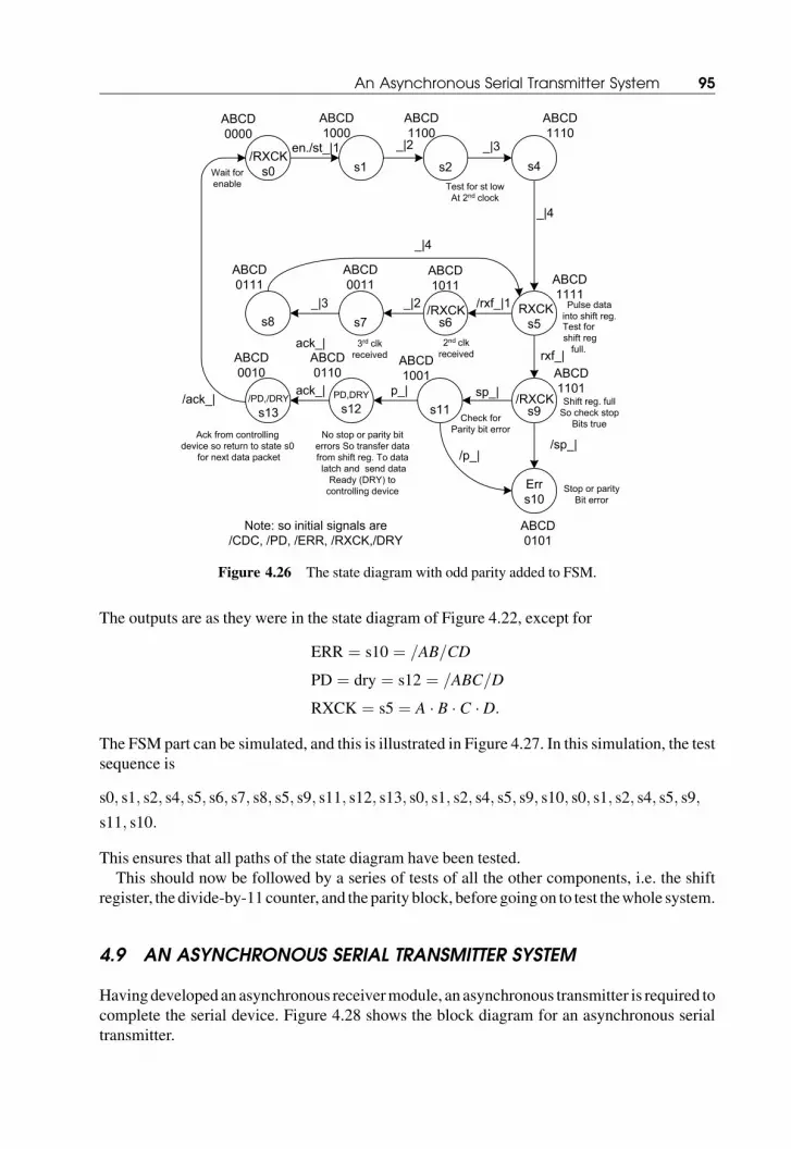
The outputs are as they were in the state diagram of Figure 4.22, except for
ERR ¼ s10 ¼ =AB=CD
PD ¼ dry ¼ s12 ¼ =ABC=D
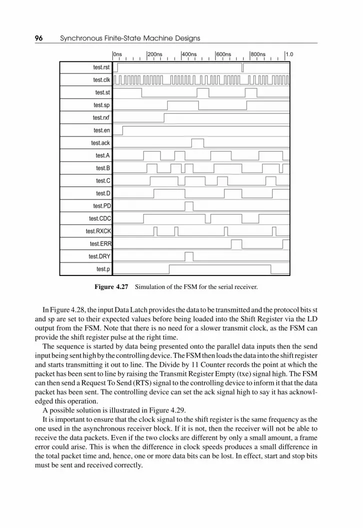
RXCK ¼ s5 ¼ A � B � C � D:The FSM part can be simulated, and this is illustrated in Figure 4.27. In this simulation, the test
sequence is
s0; s1; s2; s4; s5; s6; s7; s8; s5; s9; s11; s12; s13; s0; s1; s2; s4; s5; s9; s10; s0; s1; s2; s4; s5; s9;
s11; s10:
This ensures that all paths of the state diagram have been tested.
This should now be followed by a series of tests of all the other components, i.e. the shift
register, the divide-by-11 counter, and the parity block, beforegoingon to test thewhole system.
4.9 AN ASYNCHRONOUS SERIAL TRANSMITTER SYSTEM
Havingdeveloped an asynchronous receivermodule, an asynchronous transmitter is required to
complete the serial device. Figure 4.28 shows the block diagram for an asynchronous serial
transmitter.
/RXCK
s0 s2s1 s4
RXCK
s5s6s7s8
s9
Err
s10
/PD,/DRY
s13
en./st_|1 _|2 _|3
_|4
/rxf_|1_|2_|3
_|4
rxf_|
sp_|
/sp_|
ack_|
/ack_|
ABCD
0000
ABCD
1000
ABCD
1100
ABCD
1111
ABCD
1110
ABCD
1011
ABCD
0011
ABCD
0111
ABCD
1101
ABCD
0101
ABCD
0110
ABCD
0010
Wait for
enable Test for st low
At 2nd clock
Test for
shift reg
full.2nd clk
received3rd clk
received
Shift reg. full
So check stop
Bits true
Stop or parity
Bit error
No stop or parity bit
errors So transfer data
from shift reg. To data
latch and send data
Ready (DRY) to
controlling device
Ack from controlling
device so return to state s0
for next data packet
Note: so initial signals are
/CDC, /PD, /ERR, /RXCK,/DRY
s11
PD,DRY
s12
p_|ack_|
ABCD
1001
/p_|
Check for
Parity bit error
Pulse data
into shift reg./RXCK
/RXCK
Figure 4.26 The state diagram with odd parity added to FSM.
An Asynchronous Serial Transmitter System 95
In Figure 4.28, the inputData Latch provides the data to be transmitted and the protocol bits st
and sp are set to their expected values before being loaded into the Shift Register via the LD
output from the FSM. Note that there is no need for a slower transmit clock, as the FSM can
provide the shift register pulse at the right time.
The sequence is started by data being presented onto the parallel data inputs then the send
inputbeingsenthighby thecontrollingdevice.TheFSMthen loads thedata into the shift register
and starts transmitting it out to line. The Divide by 11 Counter records the point at which the
packet has been sent to line by raising the Transmit Register Empty (txe) signal high. The FSM
can then send a Request To Send (RTS) signal to the controlling device to inform it that the data
packet has been sent. The controlling device can set the ack signal high to say it has acknowl-
edged this operation.
A possible solution is illustrated in Figure 4.29.
It is important to ensure that the clock signal to the shift register is the same frequency as the
one used in the asynchronous receiver block. If it is not, then the receiver will not be able to
receive the data packets. Even if the two clocks are different by only a small amount, a frame
error could arise. This is when the difference in clock speeds produces a small difference in
the total packet time and, hence, one or more data bits can be lost. In effect, start and stop bits
must be sent and received correctly.
0ns 200ns 400ns 600ns 800ns 1.0
test.rst
test.clk
test.st
test.sp
test.rxf
test.en
test.ack
test.A
test.B
test.C
test.D
test.PD
test.CDC
test.RXCK
test.ERR
test.DRY
test.p
Figure 4.27 Simulation of the FSM for the serial receiver.
96 Synchronous Finite-State Machine Designs

Total packet time ¼ 11� 1=ðclock frequencyÞ:
For example, if the transmitter shift register clock is 1 MHz (usually referred to as the baud rate),
then
Total packet time ¼ 11� 1=ð1� 106Þ ¼ 11� 1 ms ¼ 11 ms in duration:
The receiver shift register clock does have a tolerance; this is a result of the fact that the data are
sampled within a four-clock window (see Figure 4.20) and a small difference in the two packet
lengths can be accommodated.
In some commercial Universal Asynchronous Receiver Transmitter (UART) devices, 16
(rather than4) is used for the clk signal used to generate the shift register clock (RXCK), giving a
greater resolution for detecting the logic value of the data bits.
Generally, if the clocks in both the transmitter and the receiver are of a high accuracy (as one
would expect from crystal oscillators), then there is usually not a problem. It would be easy to
restructure the receiver state diagrams of Figures 4.22 and 4.26 to accommodate a higher
resolution shift register clock by addingmore states in the loop comprising s5 to s8, and adding
states between s1 to s5 for the start bit. However, such a design could make use of the One Hot
method covered in Chapter 5.
Note that the FSM clock is four times that of the baud rate.
The state diagram for the asynchronous transmitter is illustrated in Figure 4.29. In this
state diagram, the shift register is clocked every four FSM clock pulses as it moves between
Data Latch
Shift Register
FSM
Divide
By 11
counter
st d0 d1 d2 d3 d4 d5 d6 d7 OPn sp
PD
clk
LDsend txe CLKOUT
RTS ack rst
Parallel data in – from outside world
Transmit
Data out
Shift Reg
clockTransmit
Reg empty
Load Shift Register
& clear counter
Pulse
Data latch
Data
Transmitted
To controller
Acknowledge
From controller Reset system (controlled by outside
world device to reset the system)
0
Sp=1
Parity
Generator
Block
St = 0
d0
d7
Parity generator
Block Connected
to data Latch outputs
and St and sp bits
From controller
TX
d0 d1 d2 d3 d4 d5 d6 d7
Q0 Q1 Q2 Q3 Q4 Q5 Q6 Q7
.
.
ld
clr
Figure 4.28 Block diagram for an asynchronous serial transmitter.
An Asynchronous Serial Transmitter System 97

s4, s8, s9, and s5. Note that for a 1 �s baud rate the transmitter FSM clock would need to be
4 MHz.
4.9.1 Equations for the Asynchronous Serial Transmitter
A � d ¼ s0 � sendþ s1þ s2þ s3þ s4þ s5 � =txe¼ =B � =C � =D � sendþ A � =B � =Dþ A � C � =Dþ A � B � =Dþ B � =C � =D � =txe
B � d ¼ s2þ s3þ s4þ s5þ s8þ s9þ s6 � =ack¼ A � C � =Dþ B � =C þ =A � B � =D � =ack
C � d ¼ s1þ s2þ s5 � txeþ s6þ s7 � ack¼ A � =B � =Dþ =A � B � =D � txeþ =A � C � =D
D � d ¼ s4þ s8
¼ A � B � =C � =Dþ A � B � =C � D¼ A � B � =C
PD ¼ s1 ¼ A � =B � =C � =DCLKOUT ¼ s4 ¼ A � B � =C � =DLD ¼ =s2 ¼ =ðA � =B � C � =DÞRTS ¼ s6 ¼ =A � B � C � =D:
/PD,LD,/CLKOUT
/RTSs0
PD
s1
/PD, /LD
s2
LD
s3
CLKOUT
s4s5
RTS
s6
/RTS
s7
send_| _| _|
_|
_|
txe_| /txe_|ack_|
/ack_|
ABCD0000
ABCD1000
ABCD1010
ABCD1110
ABCD1100
ABCD0100
ABCD0110ABCD
0010
NOTE: Clk _| must be same as receiver FSM clock
Ready toaccept data
packet to send
Load data latch
Load shift reg.with data latch
data + st & sp bits
Shift reg.settling time
Pulseshiftreg.
Check forshift reg.empty
All data shifted outso send RTS to
controlling device.Wait for acknowledge
from controlling device
Dummy stateto obtain unit
distance coding
Controller can set send to logic 1 for duration of data packetstransactions with ack and RTS as handshakes between the controllerand asynchronous transmitter.
_|
_|
/CLKOUT
s8s9
Produceclkout
pulse every4 FSM clk
ABCD1101
ABCD0101
Figure 4.29 State diagram for the asynchronous serial transmitter.
98 Synchronous Finite-State Machine Designs

A simulation of the FSM results in the waveforms of Figure 4.30. In this simulation, the test
sequence is s0, s1, s2, s3, s4, s8, s9, s5, s4, s8, s9, s5, s6, s7, s0.
Using the asynchronous transmitter and receiver FSMs just described, it would be possible
with modern FPGAs to run at quite high baud rates, as illustrated below.
FSM clock Receiver Transmitter clock Baud rate
RXCK CLKOUT
4MHz 1MHz 1MHz 1 mega baud
8 MHz 2MHz 2MHz 2 mega baud
16 MHz 4MHz 4MHz 4 mega baud
32 MHz 8MHz 8MHz 8 mega baud
80 MHz 20MHz 20MHz 20 mega baud
Both transmit and receiver units use the same FSM clock frequency generated with their own
clock circuits.
Thehigher baud rateswouldneed to use twisted-pair cables over relatively short transmission
distances up to around 1 m. Transmission line effects would need to be taken into account, but
this is beyond the scope of this book.
0ns 100ns 200ns 300ns 400ns
test.rst
test.clk
test.send
test.txe
test.ack
test.CLKOUT
test.PD
test.LD
test.RTS
test.A
test.B
test.C
test.D
Figure 4.30 Simulation of the serial transmitter FSM.
An Asynchronous Serial Transmitter System 99
4.10 CLOCKED WATCHDOG TIMER
Mostmicrocontrollers thesedayshaveabuilt inwatchdogtimer(WDT).TheWDTisanaddressable
device that can bewritten to on a regular basis. The idea is that the timer (usually a down counter) is
regularlywritten toreinitialize it toaknowncountvalue.Betweenwrites, thecounterwillbeclocked
towardszero. If themicrocontrollerdoesnotwrite to theWDTbetweencountdownperiods, then the
counter will reset to zero and this action can be used to reset the microcontroller.
TheWDT thus acts as a safeguard to prevent themicrocontroller from running out of control
(jumping to an instruction that is not part of the program sequence), perhaps due to a transient in
the power system.
Another use is in amicroprocessor-based systemwhere the operating system (perhaps a real-
time operating system) can regularly reset theWDTand, hence, provide ameans of determining
a microprocessor system failure.
The application program running on themicrocontroller needs towrite regularly to theWDT
to prevent it from reaching the reset state.
Although most microcontrollers have this feature, a lot of microprocessor systems do not.
Therefore, a circuit would need to be designed for this purpose.
The clocked FSM system shown in Figure 4.31 is a basic system designed to perform the
action of aWDT. The system needs to be designed around the specificmemory/IO cycle timing
of the microprocessor. In Figure 4.31 the memory/IO write cycle is based around a four-clock
pulse cycle time T1 to T4.
clk
ce
iow
WDP
T1 T2 T3 T4 T1 T2
AddrAddressDecoding FSM
Down
Counter
clk
ce WDP
iow
initializeInitializecounter
Toreset
Microprocessor
Figure 4.31 Block diagram for a WDT for a microprocessor system.
100 Synchronous Finite-State Machine Designs

The system is controlled by anFSMthatmonitors the chip enable ce controlled by the address
decoding logic. This can respond to a particular address from the microprocessor. In addition,
the iow signal controlled by the microprocessor is also monitored by the FSM. When the
microprocessor addresses theWDT, ce goes low, followed by iow in theT2 clock period.On the
rising edge of the T3 clock period, the WDT pulse is generated. The FSM must produce this
watchdogpulse (WDP)at exactly the right time in thewrite cycle (T3period).Both theFSMand
the down counter are clocked by the same microprocessor clock clk.
InAppendixB, the design of a downbinary counter is described andSectionB.1 shows how this
canbedone.Toprovide this counterwith afixed startingvalue (to count down from), theflipflips of
the counter canbepreset to aknownvalue,usingaparallel loadingcounter (seeSectionB.3).This is
thepurposeoftheinitializeinputinFigure4.31(essentiallyaparallel loadinputtothedowncounter).
Note that this same input provides the initial state for the FSM (whichwill be state zero). The
WDPwill provide frequent reinitialization pulses to the down counter and, thus, prevent it from
reaching its zero state (which would otherwise cause a microprocessor reset).
A suitable state diagram is illustrated in Figure 4.32,wherein the FSMwaits in state s0 for the
microprocessor to write to the address of the WDT. This will cause ce to go low during the T1
state of the memory/IO cycle (see Figure 4.31) so that on the T2 rising clock edge the FSMwill
move into s1. Here, it waits for the microprocessor to lower iow; then, on the next clock pulse
(T3), the FSM will move into state s2, where it will lower the WDP output signal. On the next
clock pulse (T4), the FSMwillmove to s3, raising theWDP, andwait for the ce signal to go high.
Thiswill occur at the endof thememory/IOwrite cycle andwill be seenby theFSMon the rising
edge of T1.
The equations for the FSM that follow are from Figure 4.32.
/ce_|(T2)
/iow_|(T3)
_|(T4)
ce_|(T1)
WDP
s0
WDP
s1
/WDP
s2
WDP
s3
AB00
AB10
AB11
AB01
Each clock pulse corresponds to a T state
Figure 4.32 State diagram for the WDT.
Clocked Watchdog Timer 101
4.10.1 D Flip-Flop Equations
A � d ¼ s0 � =ceþ s1
¼ =A � =B � =ceþ A � =B¼ =B � ceþ A � =BB � d ¼ s1 � =iowþ s2þ s3 � =ce¼ A � =B � =iowþ A � Bþ =A � B � =ce¼ A � =iowþ A � Bþ B � =ce:
4.10.2 Output Equation
WDP ¼ =ðs2Þ ¼ =ðA � BÞ:
Theequation for cewoulddependupon thedesiredaddressassigned to theWDT.Forexample, if
the address assigned was 300h (11 0000 0000 binary), then the equation would result in
ce ¼ =ða9 � a8 � =a7 � =a6 � =a5 � =a4 � =a3 � =a2 � =a1 � =a0Þ:
0ns 50ns 100ns 150ns 200ns
test.rst
test.clk
test.ce
test.iow
test.WDP
test.A
test.B
Figure 4.33 The WDT FSM simulation.
102 Synchronous Finite-State Machine Designs
There could be additional qualifier signals, i.e. in a PC using the IOmemorymap the signal /aen
would be required in order to distinguish between dynamic memory access (DMA) cycles and
IO cycles (see Chapter 5 for DMA). Also, the /iow signal would be needed to identify a write
cycle.
The above equation for ce would then be
ce ¼ =ða9 � a8 � =a7 � =a6 � =a5 � =a4 � =a3 � =a2 � =a1 � =a0 � =aen � =iowÞ:The equations to describe the down counter are repeated below from Appendix B for conve-
nience.
Qn � t ¼Yp¼n
p¼1ð=qpÞ for an n-stage counter;with the first T mflip-flop q0 � t input ¼ 1:
This equation expands to
Q0 � t ¼ 1
Q1 � t ¼ =q0
Q2 � t ¼ =q0 � =q1Q3 � t ¼ =q0 � =q1 � =q2Q4 � t ¼ =q0 � =q1 � =q2 � =q3:
for a four-stage down counter.
Note that the counter needs anasynchronous initialization signal connected to eachTflip-flop
to form the parallel loading input logic (see Equation (B.4) and Figure B.4).
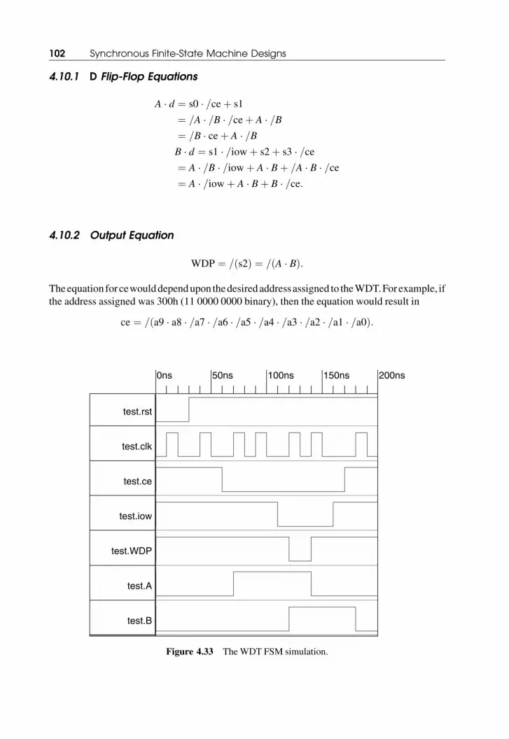
Figure 4.33 shows the FSM in action. The output WDP goes low during state s2 after the
address-decoding ce and iow have been detected going low in sequence. The FSM state
transitions are clearly seen in the flip-flop A and B outputs.
Note that in theabovesimulation there areadditional clockpulses.Thesehavebeengenerated
by the test benchgenerator to test for theFSMremaining in states s0ands1until changes in thece
and iowsignalsoccur.Thiswouldnothappen inpractice, since themicroprocessorhascontrolof
iow and the address-decoding logic ce.
4.11 SUMMARY
In thischapter, anumberofpractical exampleshavebeendevelopedusing theblockdiagramand
state diagram approach developed in the Chapters 1–3. These have then been implemented in
terms of D-type flip-flops. You may well decide to use some of these examples in your own
designs, or expand upon them to make them fit your own requirements.
In the next chapter, the idea of having a state for each D-type flip-flop will be introduced,
leading to systems that do not need secondary state variables.
Summary 103


