Embed Size (px)
Citation preview
Ss
JSa
b
ARRAA
KSHIM
1
csincbdoTma
mno
0h
Applied Surface Science 280 (2013) 424– 430
Contents lists available at SciVerse ScienceDirect
Applied Surface Science
jou rn al h omepa g e: www.elsev ier .com/ locate /apsusc
urface roughness reduction using spray-coated hydrogenilsesquioxane reflow�
iri Cecha,b, Henrik Pranovb, Guggi Kofodb, Maria Matschukb,wathi Murthyb, Rafael Taboryskia,∗
Department of Micro- and Nanotechnology, Technical University of Denmark Building 345E, DK, 2800 Kgs. Lyngby, DenmarkInMold Biosystems A/S, Gregersensvej 6H, DK, 2630 Taastrup, Denmark
a r t i c l e i n f o
rticle history:eceived 17 January 2013eceived in revised form 1 May 2013ccepted 2 May 2013vailable online 10 May 2013
eywords:urface roughnessydrogen silsesquioxane
njection molding
a b s t r a c t
Surface roughness or texture is the most visible property of any object, including injection molded plasticparts. Roughness of the injection molding (IM) tool cavity directly affects not only appearance and percep-tion of quality, but often also the function of all manufactured plastic parts. So called “optically smooth”plastic surfaces is one example, where low roughness of a tool cavity is desirable. Such tool surfaces canbe very expensive to fabricate using conventional means, such as abrasive diamond polishing or diamondturning. We present a novel process to coat machined metal parts with hydrogen silsesquioxane (HSQ)to reduce their surface roughness. Results from the testing of surfaces made from two starting rough-nesses are presented; one polished with grit 2500 sandpaper, another with grit 11.000 diamond polishingpaste. We characterize the two surfaces with AFM, SEM and optical profilometry before and after coat-
old coating ing. We show that the HSQ coating is able to reduce peak-to-valley roughness more than 20 times onthe sandpaper polished sample, from 2.44(±0.99) �m to 104(±22) nm and more than 10 times for thepaste polished sample from 1.85(±0.63) �m to 162(±28) nm while roughness averages are reduced 10and 3 times respectively. We completed more than 10,000 injection molding cycles without detectabledegradation of the HSQ coating. This result opens new possibilities for molding of affordable plastic partswith perfect surface finish.
© 2013 The Authors. Published by Elsevier B.V. All rights reserved.
. Introduction
Roughness of advanced polymer replication tools is costly andhallenging to control, especially in case of complex geometriesuch as tools for freeform optical components, for microflu-dic and medical diagnostics devices [1–3] or as substrates foranopatterned surfaces. Such applications may often require spe-ial fabrication of molding tools. Low roughness surfaces fabricatedy conventional means, such as abrasive diamond polishing oriamond turning, are often extremely costly. Hard coatings areften required to protect molds and to extend their lifetime.
hese coatings [4–6] are usually vacuum deposited [7,8] confor-al coatings that simply copy an underlying topography, withoutffecting roughness. Electroplated coatings like hard chrome can
� This is an open-access article distributed under the terms of the Creative Com-ons Attribution-NonCommercial-No Derivative Works License, which permits
on-commercial use, distribution, and reproduction in any medium, provided theriginal author and source are credited.∗ Corresponding author. Tel.: +45 21444236.
E-mail address: [email protected] (R. Taboryski).
169-4332/$ – see front matter © 2013 The Authors. Published by Elsevier B.V. All rights ttp://dx.doi.org/10.1016/j.apsusc.2013.05.004
even increase roughness. Wet deposited polymer coatings usuallydo not form sufficiently hard and durable films and the dip coatingprocess may ruin fine features of a mold surface, such as microflu-idic channels or micro- and nanopatterned regions.
Silsesquioxanes are small, cage-like, organosilicate moleculeswith the formula [RSiO3/2], with three silicate bonds per sili-con atom and one organic substituent R [9]. They tend to formcross-linked, organic-inorganic networks. Such networks maydemonstrate features of both a hard, ceramic-like materials andfeatures of a soft, organic material. Properties can be tuned andmodified by processing to achieve for instance high final hard-ness together with solution processing or spin coating. There isa wide range of applications for this sophisticated material, suchas optical coatings [10], dielectric insulators [11], barrier coatings,nanocomposites [12], or lithography [13] to name a few.
Hydrogen silsesquioxane (HSQ), where the organic substituentR is simply a hydrogen atom, is an established lithographic resist[14,15] with good contrast and high sensitivity. HSQ resist in a
solvent consist of individual cage-like molecules or a partiallycross-linked, low molecular mass oligomer. Hence, it flows and canbe spray-coated on planar and non-planar surfaces. It can be re-saturated with solvent to reduce surface roughness, as we show inreserved.

ce Sci
taPlmatAo
atct[cftnr
2
pm
2
aiTpags1ufbs
FmoswHp
tle where inert gas is introduced to the MIBK solvent and thenreintroduced back to the chamber to achieve fast exposure to theatmosphere saturated with solvent vapor. Samples are kept in thechamber for 30–60 min, at ambient temperature and pressure.
J. Cech et al. / Applied Surfa
his paper, or it can be (nano)patterned [16–18]. HSQ cross-linksfter curing and so forms a hard, fused silica-like structure.atterned HSQ surfaces have previously been used as nanoimprintithography masters [19]. Prerequisite to use HSQ for an injection
olding mold is durability and robustness, which we tested. Hence, mold comprising of such a cross-linked HSQ surface, is expectedo be able to withstand a large number of injection molding cycles.nother viable use of spray-coated HSQ film is repair/refurbishingf injection molds as they are often extremely costly to replace.
HSQ mold surfaces can be coated with additional chemicals suchs a monolayer of perfluorodecyltrichlorosilane (FDTS) which fur-her reduces surface energy, sticking and demolding force. Whileoating of SiO2 [20–23] or cured HSQ [16] nanoimprint lithographyools with an antisticking/release layer is not new, it was suggested24] and recently shown [25,26] that an FDTS monolayer coatingan be successfully used to coat certain injection molding tools. Thisurther reduction of the surface energy is important for a cost effec-ive injection molding of complex and challenging articles such asanopatterned superhydrophobic surfaces, where a successful partelease remains a challenge.
. Methods
We describe preparation of the metallic substrates, deposition,rocessing and curing of the HSQ film, sputtering of a reflectiveetallic film and characterization of the surfaces.
.1. Substrates
Our testing substrates are the machined aluminum RSA 6061lloy discs with a diameter of 33 mm and a thickness of approx-mately 3.7 mm, which may be used as an injection mold insert.he surface after machining was sanded with a series of sandpa-ers from Siawat fc, Switzerland for the grits P800, P1000, P1200nd from Rhynowet plus from Indasa, Portugal for the superfinerits P1500, P2000 and P2500. Sanding was performed in a wettate, using cca 10 min with each grit. Ceramic polishing paste MPA1,000/1 from Festool, Germany, corresponding to grit 11,000 was
sed on the appropriate sample for approximately 15 min. All sur-aces have been carefully rinsed with acetone, isopropylalcohol andlow dried in dry nitrogen after surface preparation. Aluminumubstrates have been cleaned immediately before spray-coating inig. 1. Photograph of two aluminium samples. The diameter of disks is approxi-ately 33 mm. The left sample was polished with P2500 sandpaper, and the right
ne with a polishing paste corresponding to grit 11,000. Vertical divide on eachample is the border between the left side, which was masked, and the right parthich was coated with silsesquioxane, thus having substantially lower roughness.orizontal line at the top section of each of shown samples marks an area that wasrotected by a silicon wafer during deposition of a reflective metallic film.
ence 280 (2013) 424– 430 425
the air plasma chamber for 15 min, using the chamber Diener PicoP100 from Diener Electronic, Germany to ensure perfect cleanlinessand to reduce hydrocarbon contamination on the surface.
2.2. HSQ film processing
HSQ resist, FOX 16 from Dow Corning was applied using a spray-coating technique with an ultrasonic nozzle (Sonotek ExactaCoatwith Impact spray nozzle). The resist passes through the nozzle andreaches the ultrasonically agitated nozzle tip, where it disintegratesinto a mist. The mist is forced onto the sample surface using a carrierair stream. FOX 16 resist is mixed 1:10 with methyl isobutyl ketoneas solvent, and then sprayed at a flow rate of 0.4 mL/min, with therobot passing the nozzle at 25 mm/s and line spacing of 0.88 mm.Half of sample area was masked with cleanroom blue tape, andtherefore not coated with HSQ.
2.3. Re-saturation with a solvent
Samples were transferred to the reflow chamber immediatelyafter spray-coating. The reflow chamber consists of a bubbler bot-
Fig. 2. The root mean square (RMS) roughness (top panel), the roughness average(Sa), which is normally used to describe the roughness of machined surfaces (middlepanel), and the peak-to-valley roughness (SPV) all dramatically decrease once sam-ples are coated with the hydrogen silsesquioxane (HSQ) film. This was observedon sandpaper and on paste polished samples and is valid for both optical (verticalscan interferometry [VSI]) and AFM data. VSI roughness data cannot be measuredon HSQ coated samples without coating them with a reflective film first becauseHSQ coating is transparent.
4 ce Sci
2
awwr
2
If8wrma
mca0fe
w9it
Fs
26 J. Cech et al. / Applied Surfa
.4. Curing
Samples were cured in an inert gas atmosphere oven, first for 8 ht 70 ◦C to facilitate full solvent removal and then the temperatureas ramped up to 400 ◦C for 1 h to ensure full cross-linking. Heatingas turned off and the oven temperature slowly ramped down to
oom temperature.
.5. Characterization
We used a Sensofar optical profiler in the Vertical Scannterference (VSI) mode with 5 scans per spot and a 100× DI inter-erence objective. We selected our tested area to be approximately5 × 85 �m, with the 512 × 512 pixels resolution, to be comparableith the AFM data. The pixel to pixel distance is 166 nm, compa-
able to the 176 nm for the AFM. Data was plane corrected. Weeasured 3 spots for each sample and treatment, each at least 2 mm
part.To increase reflectance of the HSQ film and to avoid light trans-
ission and reflection from the metal substrate, we sputter coatedured HSQ samples with a thin film of gold/palladium (80/20)lloy. We used the Balzers SCD 004 sputter coater, operated with.06–0.07 mBar pressure of Argon. Samples have been processedor 240 s at 30 mA current. A silicon wafer is always included toxamine the effect of sputtering on roughness.
We also characterized our sample surfaces in a tapping mode
ith an AFM PSIA XE-150. We selected the maximal area, approx.0 × 90 �m and measured it with 512 × 512 pixels resolution, giv-ng a pixel to pixel distance of 176 nm, comparable to the 166 nm forhe optical profiler. We used a BudgetSensor aluminium coated tip.
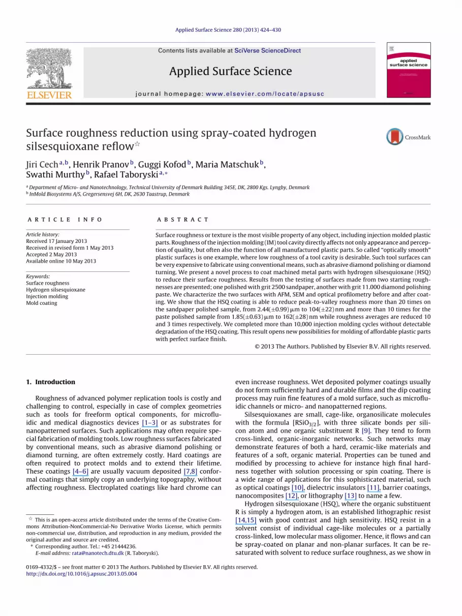
ig. 3. Atomic force microscopy data showing the topography of superfine sandpaper polhows the silsesquioxane coated and cured surface. Surface roughness is strongly reduce
ence 280 (2013) 424– 430
Collected AFM data was evaluated using XEI software, 1.8.0 Build16 from Park Systems corp.
The samples were investigated in a Zeiss Crossbeam 1540 EsB.After transfer to the scanning electron microscope (SEM) the sam-ples were tilted 54◦ relative to the beam. A focused ion beam (FIB)was used to selectively remove material from the samples in ca.10 �m wide trenches, revealing the profile, i.e. the inner structureperpendicular to the surface. The samples were imaged using 3 kVaccelerating voltage.
3. Results and discussion
Aluminum disks having two different starting roughnesses werecoated with a layer of hydrogen silsesquioxane (HSQ). The superfinesandpaper polished disk shows an initial area peak-to-valleyroughness of 2.44(±0.99) �m while the paste polished disc shows1.85(±0.63) �m. The HSQ layer was deposited by spray-coating,which is, unlike spin-coating, capable of coating non-planar sur-faces and challenging geometries such as concave optical andmicro-optical surfaces, molds for microfluidic devices and othergeometries which would be impossible to polish by manual ormechanical means. Samples that have been spray-coated with HSQand cured show considerably reduced roughness as shown in Fig. 1.The left sample is rougher as it was wet polished with superfineP2500 sandpaper, while the right sample was polished with apolishing paste corresponding to grit 11,000. We can see a verti-
cal line on each sample, dividing it into two parts. The left partwas masked and is thus uncoated, in the original state, and theright part, which was coated with HSQ, has substantially lowerroughness.ished sample surfaces. Top panel shows the uncoated surface and the bottom paneld.
ce Sci
cSsrtHatTfttsnccibCth[
Ft
J. Cech et al. / Applied Surfa
Films, spray-coated under conditions described in Section 2.2onsists of almost solvent-free particles of un-cross-linked HSQ.uch films do not reduce roughness per se; they have to be re-aturated with solvent prior to full cross-linking. However duringe-saturation with solvent, the surface energy of the soft, plas-ic, solvent re-soaked film is minimized by self-smoothing. A softSQ film reflows to achieve the minimal surface area. This statend shape is then fixed by re-evaporation of solvent, which makeshe HSQ films harder, yet still capable of a plastic deformation.his is especially true when the HSQ film is exposed to externalorces, such as nanopatterning by imprinting [27]. However, if wehermally cure a smooth, virtually solvent free film at an elevatedemperature, it fully cross-links and forms a hard coating with aubstantially reduced roughness, compared to the starting rough-ess of the metal substrate. This is demonstrated in Fig. 2. Structuralhanges in HSQ films during thermal curing, such as cross-linking,age-to-network redistribution, and film densification of the result-ng SiO2 film are already well described in literature. They haveeen studied using FTIR spectroscopy by Liu et al. [28], Yang and
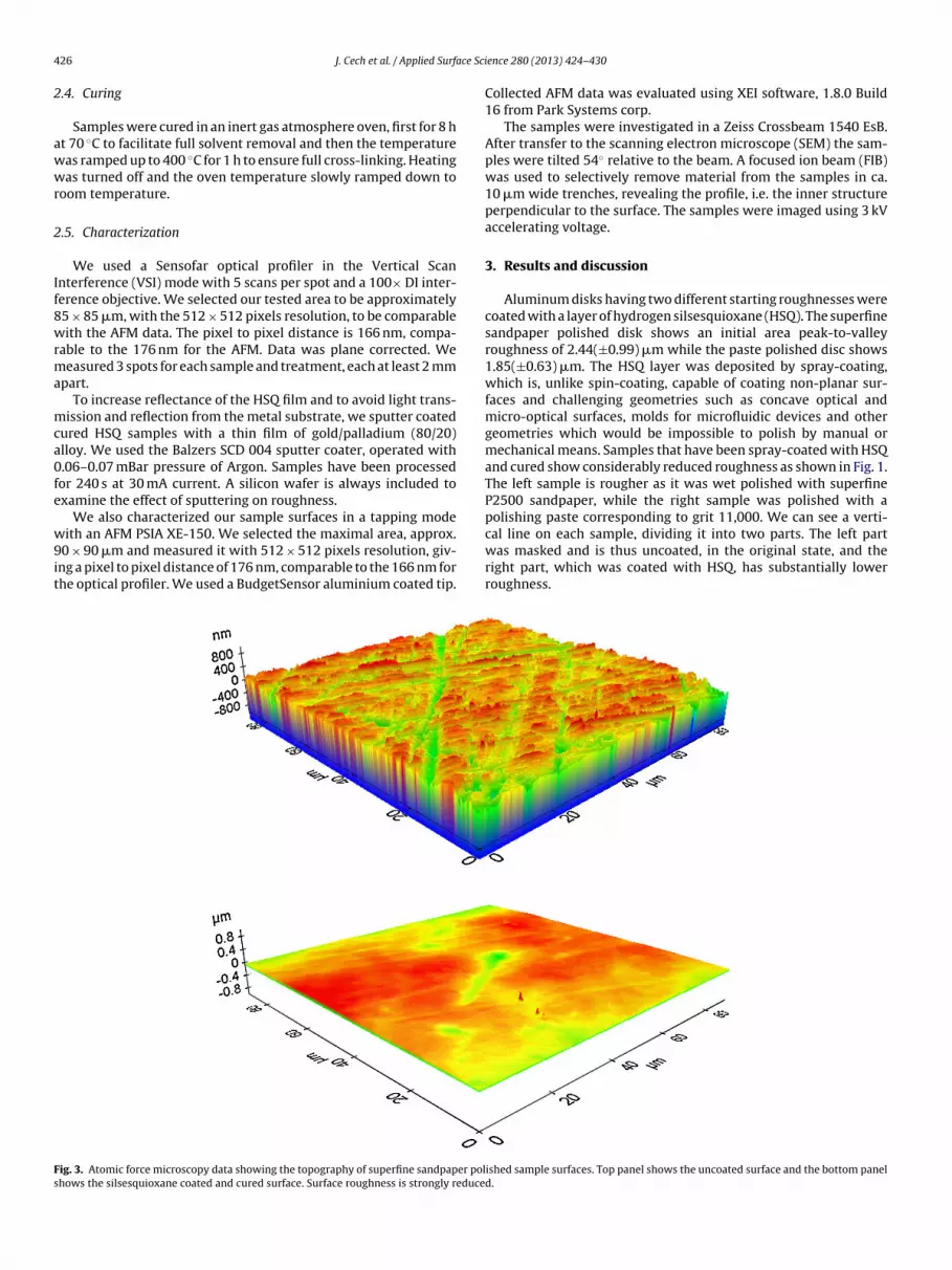
hen [29], and using Broadband coherent anti-Stokes Raman scat-ering microscopy by Caster et al. [30]. Thermally induced changesave been compared with e-beam induced changes by Choi et al.31].ig. 4. Optical profiler data showing the topography of superfine sandpaper polished samhe silsesquioxane coated and cured surface. Surface roughness is strongly reduced.
ence 280 (2013) 424– 430 427
We did not encounter issues with sublimation during heatingpossibly due to the fact that the film is partially cross-linked alreadyat room temperature. The fully cross-linked HSQ film on the metalsubstrate is capable of and has been tested to withstand more than10,000 injection molding cycles, when applied on the metal moldinsert. We have been also able to demonstrate use of HSQ resist fora mold repair and refurbishing [32].
We characterized coated and uncoated surfaces with AFM andan optical profiler. An example of AFM topography is shown in Fig. 3.For the 3-D optical profiler measurements on surfaces coated withthe cured HSQ films it was necessary to sputter a thin layer of areflective film in order to characterize roughness of HSQ coated sur-faces. This is essential as the HSQ film alone is transparent, and has,according to the literature [29], a relatively low refractive index ofabout 1.36–1.39. Hence, HSQ only reflects approximately 2.4–2.7%of incident light, assuming perpendicular incidence and no rough-ness. This, together with an uneven, rough and highly reflectivemetallic substrate surface under the HSQ prevents reliable opti-cal characterization without metallization. Neither the HSQ film
thickness nor the surface topography/roughness can be reliablymeasured without metallization.However, when sputtering of a thin, reflective layer of metalon top of the HSQ, we can increase reflectance to well over 50%
ple surfaces. Top panel shows the uncoated surface and the bottom panel shows
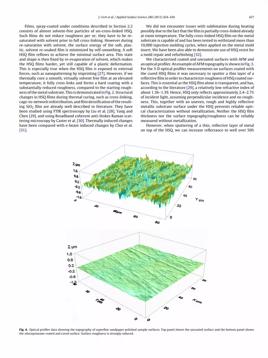
428 J. Cech et al. / Applied Surface Science 280 (2013) 424– 430
F columb ess is
weeawtofiaosu
ctWmc1acSau
(t
ig. 5. FIB-SEM micrographs showing profiles of a sandpaper polished sample (leftottom row shows surfaces with the HSQ film. Tilt angle is 54◦ and HSQ film thickn
ithout altering the surface topography significantly. Using Fresnelquations and optical constants from literature [33,34] we canasily calculate that, for instance, as little as 14 nm of gold gives
perpendicular reflectance R = 0.51 for a wavelength of 500 nm,hich is sufficient for characterization using an optical profiler and
he vertical scan interference method. One should note that theptical constants of an extremely thin (less than 15 nm) metalliclm differ slightly from the properties of the bulk metal [35,36]nd that they usually form islands and voids instead of a continu-us film. We can see this effect in the FIB-SEM profile micrographs,hown as Fig. 5, where the non-continuous metal film is seen as theppermost layer.
Therefore we sputtered thin reflective films not only on HSQoated samples but also on silicon wafer samples, to verify theopography change due to the sputtering of a reflective film.
e observed that a pristine silicon wafer sample shows rootean square roughness SRMS of 2.4 ± 0.3 nm while a sputter
oated wafer with gold-palladium reflective film shows SRMS of.96 ± 0.2 nm, and the peak-to-valley roughnesses are 16 ± 2.30 nmnd 13.6 ± 1.6 nm respectively. We can see that the topographyhange due to sputtering of a reflective film is indeed very small (seeupplementary Table S1) thus the effect is negligible. This finallyllows surface topography measurement on HSQ coated substrates
sing a 3-D optical profilometer, as shown in Fig. 4.Areal roughness parameters, root mean square (RMS) roughnessSRMS) and the roughness average (Sa) are defined as the average ofhe height deviations and the mean surface (quadratic mean), and
n) and a paste polished sample (right column). Top row shows uncoated surfaces,approximately 1.3 �m.
the arithmetic average (mean) of the 3-D roughness, taken over theevaluation area, therefore they are statistical parameters, and wepresent them in Figs. 3 and 4. They are less sensitive to outliers andmore independent from the choice of the evaluation area/regionof interest. We see substantial decrease of roughness on the HSQcoated samples; approximately 10 times for a sample with initiallyhigher roughness and 3 times for a sample with initially lowerroughness.
For the peak-to-valley roughness (SPV), defined as being the dis-tance from the highest to the lowest point in the evaluation area,the decrease is the most dramatic one, as shown Fig. 2. We seea more than 20 times lower value for the sample with a higherstarting roughness and a more than 10 times lower value for thepaste polished sample with a lower starting roughness. Despite thefact that the peak-to-valley roughness is the one most affected bythe region-of-interest-selection, and unlike the roughness averageand the root mean square roughness it is not a statistically robustparameter, it is a very a important parameter since it dominatesthe sample appearance, the optical properties and the perceptionof quality. Even samples with decent, fairly low Sa and SRMS caneasily be ruined by a few deep scratches, thus, the reduction of thepeak-to-valley roughness is a very important effect.
We see a very good correspondence between results from two
fully independent methods, AFM and 3-D optical profilometry(after deposition of a reflective film) as can be seen by comparingFigs. 3 and 4. This result is in agreement with the FIB-SEM micro-graphs, presented in Fig. 5. We can see cross-sections of a sandpaper
ce Sci
pppiucsno
4
srdIpw
tsrtt
Hitcsf
A
tp“atBm
A
f2
R
[
[
[
[
[
[
[
[
[
[
[
[
[
[
[
[
[
[
[
J. Cech et al. / Applied Surfa
olished surface with a visible tool marks in the left column and aaste polished surface in the right column. The bottom row showsrofiles of same surfaces coated with a cured HSQ film. We can eas-
ly see an apparent film thickness and un-even morphology of annderlying metal substrate. With a known tilt angle and scale wean calculate The HSQ film thickness of approximately 1.3 �m forelected spray parameters. We can also directly see a low rough-ess top surface, with islands and voids of metal from a depositionf a reflective film.
. Conclusion
We observed smoothing of HSQ spray-coated and solvent re-aturated films on rough and polished metallic substrates. Thiseduction of surface roughness was measured with two indepen-ent methods, Atomic Force Microscopy (AFM) and Vertical Scan
nterference (VSI) optical profilometry and their results are in aerfect agreement. Sample cross-sections micrographs, measuredith a FIB-SEM confirms the same result.
The peak-to-valley surface roughness (SPV) was reduced morehan 20 times for an initially rougher sample, wet polished withuperfine sandpaper and more than 10 times for an initially lessough sample, polished with paste. The roughness average (Sa) andhe root mean square roughness (SRMS) were reduced 10 and 3imes, for the rougher and smoother substrates, respectively.
In conclusion, we have been able to show that a relatively thinSQ film on metallic substrates such as molds for injection molding
s able to greatly to decrease surface roughness. This is impor-ant, since such coating can withstand more than 10,000 moldingycles and is capable of reducing roughness on otherwise inacces-ible surfaces and geometries. This result opens new possibilitiesor molding affordable plastic parts with perfect finish.
cknowledgment
This work was funded and supported by the DTU Nanotech,he Danish National Advanced Technology Foundation (HTF)rojects “Integrated Camera Module” (grant no. 051-2008-3) andAdvanced Technology Platform NanoPlast” (grant no. 007-2010-2)nd the Copenhagen Graduate School for Nanoscience and Nano-echnology (C:O:N:T). Authors would like to thank Dr. Kathrinejørneboe from the Danish Technological Institute for the FIB-SEMicrographs and Dr. Eric Jensen for proofreading.
ppendix A. Supplementary data
Supplementary data associated with this article can beound, in the online version, at http://dx.doi.org/10.1016/j.apsusc.013.05.004.
eferences
[1] S. Tanzi, P.F. Ostergaard, M. Matteucci, T.L. Christiansen, J. Cech, R. Marie, R.Taboryski, Fabrication of combined-scale nano- and microfluidic polymer sys-tems using a multilevel dry etching, electroplating and molding process, Journalof Micromechanics and Microengineering 22 (2012) 115008, 10.1088/0960-1317/22/11/115008.
[2] P.F. Ostergaard, M. Matteucci, W. Reisner, R. Taboryski, DNA barcoding viacounterstaining with AT/GC sensitive ligands in injection-molded all-polymernanochannel devices, Analyst (2013).
[3] K.O. Andresen, M. Hansen, M. Matschuk, S.T. Jepsen, H.S. Sorensen, P. Utko, D.Selmeczi, T.S. Hansen, N.B. Larsen, N. Rozlosnik, R. Taboryski, Injection moldedchips with integrated conducting polymer electrodes for electroporation ofcells, Journal of Micromechanics and Microengineering 20 (2010) 055010,
10.1088/0960-1317/20/5/055010.[4] C. Mitterer, F. Holler, D. Reitberger, E. Badisch, M. Stoiber, C. Lugmair, R.Nobauer, T. Muller, R. Kullmer, Industrial applications of PACVD hard coatings,Surface and Coatings Technology 163 (2003), PII S0257-8972(02)00685-0.doi:10.1016/S0257-8972(02)00685-0.
[
ence 280 (2013) 424– 430 429
[5] C.H. Hsu, D. Huang, W. Ho, L. Huang, C. Chang, Characteristics and performanceof Cr2O3/CrN double-layered coatings deposited by cathodic arc plasma depo-sition, Materials Science and Engineering A – Structural Materials PropertiesMicrostructure and Processing 429 (2006), 10.1016/j.msea.2006.05.108.
[6] C.A.N. Estima, V.F. Neto, M.S.A. Oliveira, J. Gracio, Nanocrystalline diamondcoating on non-planar silicon substrates, Journal for Nanoscience and Nano-technology 12 (2012) 6700–6706, doi:10.1166/jnn.2012.4567.
[7] K. Bobzin, R. Nickel, N. Bagcivan, F.D. Manz, PVD – coatings in injection moldingmachines for processing optical polymers, Plasma Processes and Polymers 4(2007), doi:10.1002/ppap.200730507.
[8] K. Bobzin, N. Bagcivan, M. Ewering, A. Gillner, S. Beckemper, C. Hartmann,S. Theiss, Nano Structured Physical Vapor Deposited Coatings by Means ofPicosecond Laser Radiation, Journal of Nanoscience and Nanotechnology. 11(2011), doi:10.1166/jnn.2011.3468.
[9] R. Baney, M. Itoh, A. Sakakibara, T. Suzuki, Silsesquioxanes, Chemical Reviews95 (1995) 1409–1430, doi:10.1021/cr00037a012.
10] J. Zhao, I. Malik, T. Ryan, E. Ogawa, P. Ho, W. Shih, A. McKerrow, K. Taylor,Thermomechanical properties and moisture uptake characteristics of hydrogensilsesquioxane submicron films, Applied Physics Letters 74 (1999) 944–946,doi:10.1063/1.123417.
11] W. Volksen, R.D. Miller, G. Dubois, Low dielectric constant materials, ChemicalReviews 110 (2010) 56–110, doi:10.1021/cr9002819.
12] R. Kannan, H. Salacinski, P. Butler, A. Seifalian, Polyhedral oligomericsilsesquioxane nanocomposites: the next generation material for biomed-ical applications, Accounts of Chemical Research 38 (2005) 879–884,doi:10.1021/ar050055b.
13] A.E. Grigorescu, C.W. Hagen, Resists for sub-20-nm electron beam lithogra-phy with a focus on HSQ: state of the art, Nanotechnology 20 (2009) 292001,http://dx.doi.org/10.1088/0957-4484/20/29/292001.
14] H.F. Yang, A.Z. Jin, Q. Luo, C.Z. Gu, Z. Cui, Y.F. Chen, Low-energy electron-beam lithography of hydrogen silsesquioxane, Microelectronic Engineering 83(2006), doi:10.1016/j.mee.2006.01.004.
15] J.K.W. Yang, B. Cord, H. Duan, K.K. Berggren, J. Klingfus, S. Nam, K. Kim, M.J.Rooks, Understanding of hydrogen silsesquioxane electron resist for sub-5-nm-half-pitch lithography, Journal of Vacuum Science Technology B 27 (2009),doi:10.1116/1.3253652.
16] H.W. Ro, V. Popova, L. Chen, A.M. Forster, Y. Ding, K.J. Alvine, D.J. Krug, R.M.Laine, C.L. Soles, Cubic silsesquioxanes quioxanes as a green, high-performancemold material for nanoimprint lithography, Advanced Materials 23 (2011),doi:10.1002/adma.201001761.
17] S. Matsui, Y. Igaku, H. Ishigaki, J. Fujita, M. Ishida, Y. Ochiai, M. Komuro,H. Hiroshima, Room temperature replication in spin on glass by nanoim-print technology, Journal of Vacuum Science & Technology B 19 (2001),doi:10.1116/1.1417547.
18] Y. Kang, M. Okada, S. Omoto, Y. Haruyama, K. Kanda, S. Matsui, Room temper-ature nanoimprinting using spin-coated hydrogen silsesquioxane with highboiling point solvent, Journal of Vacuum Science and Technology B 29 (2011)06FC03, doi:10.1116/1.3653227.
19] D. Morecroft, J.K.W. Yang, S. Schuster, K.K. Berggren, Q. Xia, W. Wu, R.S.Williams, Sub-15 nm nanoimprint molds and pattern transfer, Journal of Vac-uum Science & Technology B 27 (2009) 2837–2840, doi:10.1116/1.3264670.
20] G. Jung, Z. Li, W. Wu, Y. Chen, D. Olynick, S. Wang, W. Tong, R. Williams, Vapor-phase self-assembled monolayer for improved mold release in nanoimprintlithography, Langmuir 21 (2005) 1158–1161, doi:10.1021/la0476938.
21] W. Zhou, J. Zhang, Y. Liu, X. Li, X. Niu, Z. Song, G. Min, Y. Wan, L. Shi,S. Feng, Characterization of anti-adhesive self-assembled monolayer fornanoimprint lithography, Applied Surface Science 255 (2008) 2885–2889,doi:10.1016/j.apsusc.2008.08.045.
22] H. Schift, S. Saxer, S. Park, C. Padeste, U. Pieles, J. Gobrecht, Controlled co-evaporation of silanes for nanoimprint stamps, Nanotechnology 16 (2005)S171–S175.
23] H. Li, X. Li, Q. Wang, H. Li, X. Li, Q. Wang, X. Li, The preparation of anti-stickinglayers on stamps of nano-imprint lithography technology via vapor deposi-tion process, Shanghai Jiaotong Daxue Xuebao/Journal of Shanghai JiaotongUniversity 41 (2007), 1687–1689+1694.
24] N.B. Larsen, S.B., Nyrup, H. Pranov, Transferring heat sensitive material on poly-mer surface for e.g. biotechnology application, comprises applying material toshaping surface at specific temperature, contacting with heated polymer, andtransferring material to polymer surface. WO2006097483-A1; EP1863621-A1.
25] J. Cech, R. Taboryski, Stability of FDTS monolayer coating on aluminuminjection molding tools, Applied Surface Science 259 (2012) 538–541,doi:10.1016/j.apsusc.2012.07.078.
26] V. Miikkulainen, M. Suvanto, T.A. Pakkanen, S. Siitonen, P. Karvinen, M.Kuittinen, H. Kisonen, Thin films of MoN, WN, and perfluorinated silanedeposited from dimethylamido precursors as contamination resistant coatingson micro-injection mold inserts, Surface and Coatings Technology 202 (2008),doi:10.1016/j.surfcoat.2008.05.007.
27] G. Kofod, Reflow polishing of injection molds, November 19–20, in: WorkshopSteel Polishing, Aachen, Germany, 2012.
28] W.C. Liu, C.C. Yang, W.C. Chen, B.T. Dai, M.S. Tsai, The structural transforma-tion and properties of spin-on poly(silsesquioxane) films by thermal curing,
Journal of Non-Crystalline Solids 311 (2002) 233–240, doi:10.1016/S0022-3093(02)01373-X.29] C. Yang, W. Chen, The structures and properties of hydrogen silsesquioxane(HSQ) films produced by thermal curing, Journal of Materials Chemistry 12(2002) 1138–1141, doi:10.1039/b107697n.

4 ce Sci
[
[
[
[
[
[in situ transmission ellipsometry and intensity measurements, Thin Solid Films455 (2004) 443–449, doi:10.1016/j.tsf.2003.11.243.
30 J. Cech et al. / Applied Surfa
30] A.G. Caster, S. Kowarik, A.M. Schwartzberg, O. Nicolet, S. Lim, S.R. Leone, Observ-ing hydrogen silsesquioxane cross-linking with broadband CARS, Journal ofRaman Spectroscopy 40 (2009) 770–774, doi:10.1002/jrs.2190.
31] S. Choi, M.J. Word, V. Kumar, I. Adesida, Comparative study of thermally curedand electron-beam-exposed hydrogen silsesquioxane resists, Journal of Vac-
uum Science & Technology B 26 (2008) 1654–1659, doi:10.1116/1.2960565.32] H. Pranov, G. Kofod, S. Murthy, Mold repair test, in: Inmold Biosystems Com-pany Records, 2012.
33] E.D. Palik, Handbook of Optical Constants of Solids, Elsevier Science & Tech.,San Diego, California, 1985.
[
ence 280 (2013) 424– 430
34] P. Johnson, R. Christy, Optical constants of noble metals, Physical Review B 6(1972) 4370–4379, doi:10.1103/PhysRevB.6.4370.
35] G. Pribil, B. Johs, N. Ianno, Dielectric function of thin metal films by combined
36] M. Novotny, J. Bulir, J. Lancok, P. Pokorny, M. Bodnar, In-situ monitoring ofthe growth of nanostructured aluminum thin film, Journal of Nanophotonics 5(2011), doi:10.1117/1.3543816.


