Embed Size (px)
Citation preview
IEEE TRANSACTIONS ON APPLIED SUPERCONDUCTIVITY, VOL. 15, NO. 2, JUNE 2005 249
Superconductor Digital Receiver ComponentsAlex Kirichenko, Saad Sarwana, Deepnarayan Gupta, and Daniel Yohannes
Abstract—We have developed and experimentally demonstratedseveral new RSFQ circuits, designed as components for digitalreceivers that are being developed by HYPRES. The first circuit isa digital phase generator, which produces a periodic digital signalwith a controllable phase shift. This signal is obtained by decima-tion of an external high frequency signal by a factor of 1024, andprovides a controllable phase shift with digital precision of 512.The second circuit, a precise digital static frequency divider, iscapable of dividing of an input signal frequency by any integervalue between 1 and 1024. The third circuit is a digital quadraturemixer performing digital downconversion of bit-stream data. Thisreport presents results of experimental evaluation of these circuitsat speeds in excess of 30 GHz.
Index Terms—Digital signal processors, HF receivers, static fre-quency dividers, superconducting integrated circuits.
I. INTRODUCTION
Adirect digital receiver of wideband radio frequency signalsis an attractive application for superconductor digital elec-
tronics. In this paper, we report the development of circuit com-ponents for realization of two types of digital receivers devel-oped at HYPRES.
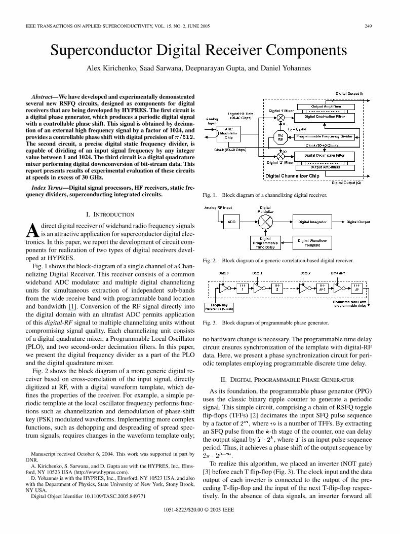
Fig. 1 shows the block-diagram of a single channel of a Chan-nelizing Digital Receiver. This receiver consists of a commonwideband ADC modulator and multiple digital channelizingunits for simultaneous extraction of independent sub-bandsfrom the wide receive band with programmable band locationand bandwidth [1]. Conversion of the RF signal directly intothe digital domain with an ultrafast ADC permits applicationof this digital-RF signal to multiple channelizing units withoutcompromising signal quality. Each channelizing unit consistsof a digital quadrature mixer, a Programmable Local Oscillator(PLO), and two second-order decimation filters. In this paper,we present the digital frequency divider as a part of the PLOand the digital quadrature mixer.
Fig. 2 shows the block diagram of a more generic digital re-ceiver based on cross-correlation of the input signal, directlydigitized at RF, with a digital waveform template, which de-fines the properties of the receiver. For example, a simple pe-riodic template at the local oscillator frequency performs func-tions such as channelization and demodulation of phase-shiftkey (PSK) modulated waveforms. Implementing more complexfunctions, such as dehopping and despreading of spread spec-trum signals, requires changes in the waveform template only;
Manuscript received October 6, 2004. This work was supported in part byONR.
A. Kirichenko, S. Sarwana, and D. Gupta are with the HYPRES, Inc., Elms-ford, NY 10523 USA (http://www.hypres.com).
D. Yohannes is with the HYPRES, Inc., Elmsford, NY 10523 USA, and alsowith the Department of Physics, State University of New York, Stony Brook,NY USA.
Digital Object Identifier 10.1109/TASC.2005.849771
Fig. 1. Block diagram of a channelizing digital receiver.
Fig. 2. Block diagram of a generic correlation-based digital receiver.
Fig. 3. Block diagram of programmable phase generator.
no hardware change is necessary. The programmable time delaycircuit ensures synchronization of the template with digital-RFdata. Here, we present a phase synchronization circuit for peri-odic templates employing programmable discrete time delay.
II. DIGITAL PROGRAMMABLE PHASE GENERATOR
As its foundation, the programmable phase generator (PPG)uses the classic binary ripple counter to generate a periodicsignal. This simple circuit, comprising a chain of RSFQ toggleflip-flops (TFFs) [2] decimates the input SFQ pulse sequenceby a factor of , where is a number of TFFs. By extractingan SFQ pulse from the -th stage of the counter, one can delaythe output signal by , where is an input pulse sequenceperiod. Thus, it achieves a phase shift of the output sequence by
.To realize this algorithm, we placed an inverter (NOT gate)
[3] before each T flip-flop (Fig. 3). The clock input and the dataoutput of each inverter is connected to the output of the pre-ceding T-flip-flop and the input of the next T-flip-flop respec-tively. In the absence of data signals, an inverter forward all
1051-8223/$20.00 © 2005 IEEE
250 IEEE TRANSACTIONS ON APPLIED SUPERCONDUCTIVITY, VOL. 15, NO. 2, JUNE 2005
Fig. 4. Functionality test of the PPG.
Fig. 5. Photograph of a 5-mm chip fabricated using HYPRES’ 1 kA=cmprocess with a 10-bit programmable phase generator.
clock pulses to its output. When an SFQ pulse is sent to the datainput of the inverter, it skips the following clock pulse. Thus, bysending an -bit binary number to the control port of the de-vice, we achieve a phase shift the output signal by .
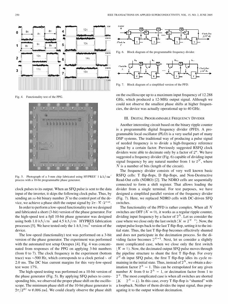
In order to perform a low-speed functionality test we designedand fabricated a short (3-bit) version of the phase generator. Forthe high-speed test a full 10-bit phase generator was designedusing both 1.0 and 4.5 HYPRES fabricationprocesses [5]. We have tested only the 1- version of thedevice.
The low-speed (functionality) test was performed on a 3-bitversion of the phase generator. The experiment was performedwith the automated test setup Octopux [4]. Fig. 4 was concate-nated from responses of the PPG on applying 3-bit numbers(from 0 to 7). The clock frequency in the experiment (bottomtrace) was 500 Hz, which corresponds to a clock period of2.0 ms. The DC bias current margins for this very-low-speedtest were 17%.
The high-speed testing was performed on a 10-bit version ofthe phase generator (Fig. 5). By applying SFQ pulses to corre-sponding bits, we observed the proper phase shift on the oscillo-scope. The minimum phase shift of the 10-bit phase generator is
. We could clearly observe the phase shift
Fig. 6. Block diagram of the programmable frequency divider.
Fig. 7. Block diagram of a simplified version of the PFD.
on the oscilloscope up to a maximum input frequency of 12.288GHz, which produced a 12-MHz output signal. Although wecould not observe the smallest phase shifts at higher frequen-cies, the device was actually operational up to 40 GHz.
III. DIGITAL PROGRAMMABLE FREQUENCY DIVIDER
Another interesting circuit based on the binary ripple counteris a programmable digital frequency divider (PFD). A pro-grammable local oscillator (PLO) is a very useful part of manyDSP systems. The traditional way of producing a pulse signalof needed frequency is to divide a high-frequency referencesignal by a certain factor. Previously suggested RSFQ clockdividers were able to decimate only by a factor of . We havesuggested a frequency divider (Fig. 6) capable of dividing inputsignal frequency by any natural number from 1 to , where
is a number of bits (length of the circuit).The frequency divider consists of very well known basic
RSFQ cells: T flip-flops, D flip-flops, and Non-DestructiveRead-Out cells (NDRO) [2]. The NDRO cells are sequentiallyconnected to form a shift register. That allows loading thedivider from a single terminal. For test purposes, we havedesigned a simplified parallel version of the frequency divider(Fig. 7). Here, we replaced NDRO cells with DC-driven SFQswitches.
The functionality of the PFD is rather complex. When allswitches are OFF , it works as a regular ripple counter,dividing input frequency by a factor of . Let us consider thecase where we close only the last switch . Now, theoutput pulse loops back to the last T flip-flop, setting it to the ini-tial state. Thus, the last T flip-flop becomes effectively shuntedand does not participate in the decimation process. So the di-viding factor becomes . Next, let us consider a slightlymore complicated case, when we close only the first switch
. Now, the decimated output SFQ pulse moves throughthe pipeline structure to shunt the first T flip-flop. For every
-th input SFQ pulse, the first T flip-flop idles its cycle re-maining in the initial state. Thus, instead of , we obtain a dec-imation factor . This can be extrapolated for any givennumber from 0 to , or decimation factor from 1 to
. The most complicated case is when all switches are shorted. In this case, every T flip-flop is “shunted” with
a loopback. Neither of them divides the input signal, thus prop-agating it to the output without decimation.
KIRICHENKO et al.: SUPERCONDUCTOR DIGITAL RECEIVER COMPONENTS 251
Fig. 8. Layout fragment of 2 bits of the programmable frequency divider.
Fig. 9. Functionality test of the 4-bit programmable frequency divider.
A 2-bit fragment of the PFD layout is -shown in Fig. 8. Thesize of a single stage of the PFD is for HY-PRESs old 3- design rules [5]. This fragment is of the par-allel version of the PFD (Fig. 7). We have designed and fab-ricated two programmable frequency dividers: a 4-bit (short)version for low-speed (functionality) testing and a 10-bit forhigh-speed testing.
The results of a low-speed (functionality) test of the 4-bit PFDare shown in Fig. 9. Here, we apply a low-frequency clock (2kHz) to the bottom trace, set different 4-bit factors by currentlevels on DC-driven switches (the next four traces), and mon-itor the output voltage from the toggling SFQ-to-DC converter(upper trace). As one can see in the picture, the 4-bit PFD dec-imates the input clock pulses by a factor of 16 for , by 5for , and by 10 for . It takes 16 clock pulsesfor transitioning from one frequency to another. This number ofclock pulses is needed to clean up the shift register (Fig. 7). Wehave checked DC bias current margins for all 16 numbers. Theminimal margin was 8% for and the maximum marginwas 22% for .
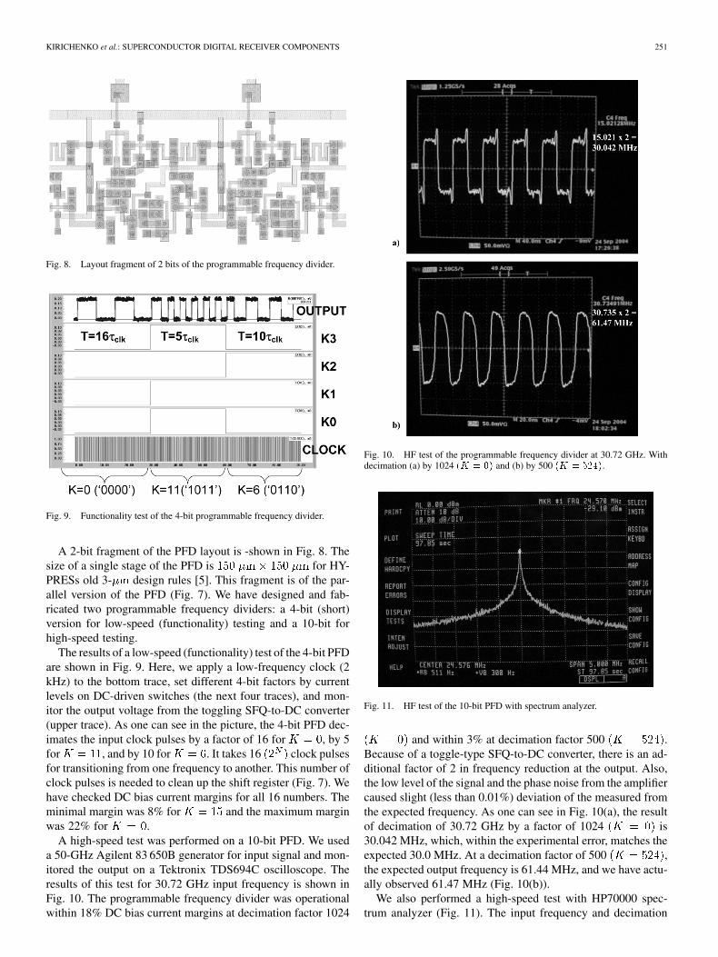
A high-speed test was performed on a 10-bit PFD. We useda 50-GHz Agilent 83 650B generator for input signal and mon-itored the output on a Tektronix TDS694C oscilloscope. Theresults of this test for 30.72 GHz input frequency is shown inFig. 10. The programmable frequency divider was operationalwithin 18% DC bias current margins at decimation factor 1024
Fig. 10. HF test of the programmable frequency divider at 30.72 GHz. Withdecimation (a) by 1024 (K = 0) and (b) by 500 (K = 524).
Fig. 11. HF test of the 10-bit PFD with spectrum analyzer.
and within 3% at decimation factor 500 .Because of a toggle-type SFQ-to-DC converter, there is an ad-ditional factor of 2 in frequency reduction at the output. Also,the low level of the signal and the phase noise from the amplifiercaused slight (less than 0.01%) deviation of the measured fromthe expected frequency. As one can see in Fig. 10(a), the resultof decimation of 30.72 GHz by a factor of 1024 is30.042 MHz, which, within the experimental error, matches theexpected 30.0 MHz. At a decimation factor of 500 ,the expected output frequency is 61.44 MHz, and we have actu-ally observed 61.47 MHz (Fig. 10(b)).
We also performed a high-speed test with HP70000 spec-trum analyzer (Fig. 11). The input frequency and decimation
252 IEEE TRANSACTIONS ON APPLIED SUPERCONDUCTIVITY, VOL. 15, NO. 2, JUNE 2005
Fig. 12. Block-diagram of the digital I/Q square-wave mixer.
factor were set to 24.576 GHz and 500 . The ex-pected output was 24.576 MHz (taking into account the addi-tional factor of 2). We observed a single peak at the expectedfrequency indicating the absence of systematic errors in the de-vice.
We have tested the digital programmable frequency dividerat up to 40 GHz clock frequency. The circuit starts malfunc-tioning at at frequencies above 31 GHz. We havealso designed a PFD for the 4.5 HYPRES’ fabricationprocess [5] and expect its maximum speed to be around 60 GHz.
IV. DIGITAL I/Q MIXER
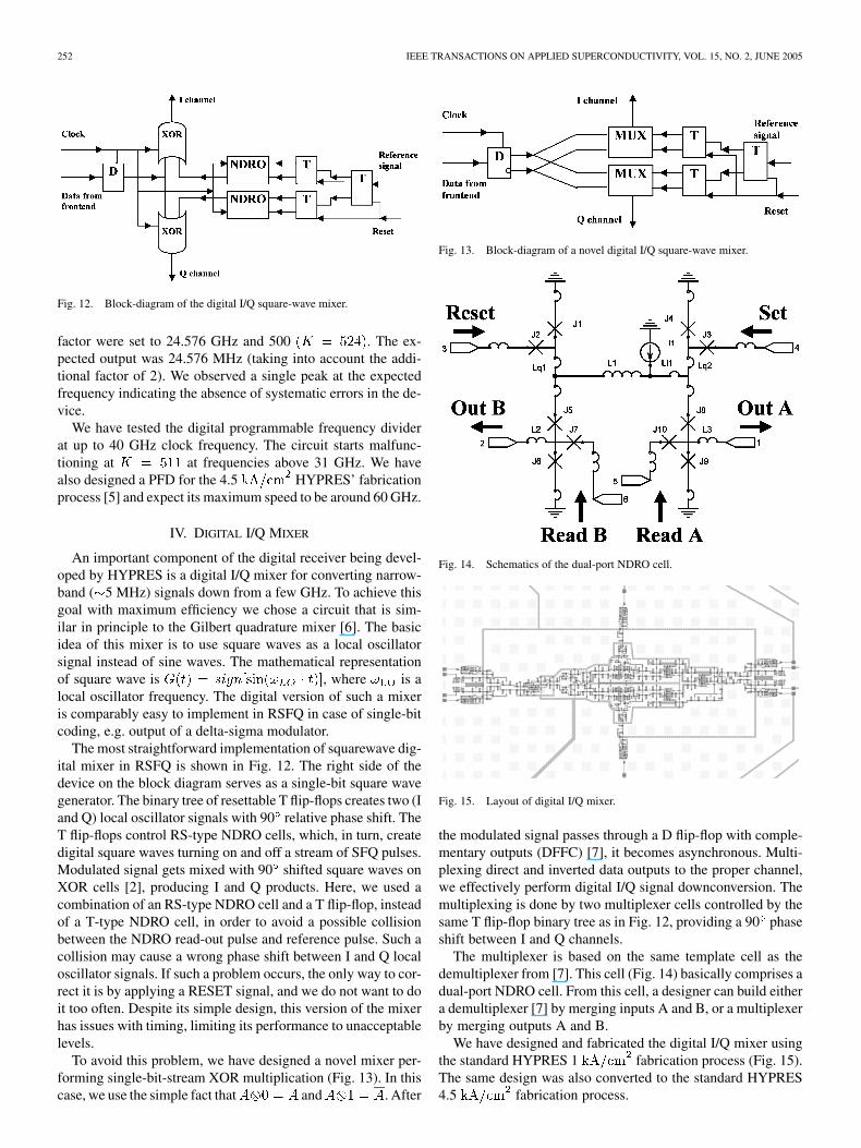
An important component of the digital receiver being devel-oped by HYPRES is a digital I/Q mixer for converting narrow-band ( 5 MHz) signals down from a few GHz. To achieve thisgoal with maximum efficiency we chose a circuit that is sim-ilar in principle to the Gilbert quadrature mixer [6]. The basicidea of this mixer is to use square waves as a local oscillatorsignal instead of sine waves. The mathematical representationof square wave is , where is alocal oscillator frequency. The digital version of such a mixeris comparably easy to implement in RSFQ in case of single-bitcoding, e.g. output of a delta-sigma modulator.
The most straightforward implementation of squarewave dig-ital mixer in RSFQ is shown in Fig. 12. The right side of thedevice on the block diagram serves as a single-bit square wavegenerator. The binary tree of resettable T flip-flops creates two (Iand Q) local oscillator signals with 90 relative phase shift. TheT flip-flops control RS-type NDRO cells, which, in turn, createdigital square waves turning on and off a stream of SFQ pulses.Modulated signal gets mixed with 90 shifted square waves onXOR cells [2], producing I and Q products. Here, we used acombination of an RS-type NDRO cell and a T flip-flop, insteadof a T-type NDRO cell, in order to avoid a possible collisionbetween the NDRO read-out pulse and reference pulse. Such acollision may cause a wrong phase shift between I and Q localoscillator signals. If such a problem occurs, the only way to cor-rect it is by applying a RESET signal, and we do not want to doit too often. Despite its simple design, this version of the mixerhas issues with timing, limiting its performance to unacceptablelevels.
To avoid this problem, we have designed a novel mixer per-forming single-bit-stream XOR multiplication (Fig. 13). In thiscase, we use the simple fact that and . After
Fig. 13. Block-diagram of a novel digital I/Q square-wave mixer.
Fig. 14. Schematics of the dual-port NDRO cell.
Fig. 15. Layout of digital I/Q mixer.
the modulated signal passes through a D flip-flop with comple-mentary outputs (DFFC) [7], it becomes asynchronous. Multi-plexing direct and inverted data outputs to the proper channel,we effectively perform digital I/Q signal downconversion. Themultiplexing is done by two multiplexer cells controlled by thesame T flip-flop binary tree as in Fig. 12, providing a 90 phaseshift between I and Q channels.
The multiplexer is based on the same template cell as thedemultiplexer from [7]. This cell (Fig. 14) basically comprises adual-port NDRO cell. From this cell, a designer can build eithera demultiplexer [7] by merging inputs A and B, or a multiplexerby merging outputs A and B.
We have designed and fabricated the digital I/Q mixer usingthe standard HYPRES 1 fabrication process (Fig. 15).The same design was also converted to the standard HYPRES4.5 fabrication process.
KIRICHENKO et al.: SUPERCONDUCTOR DIGITAL RECEIVER COMPONENTS 253
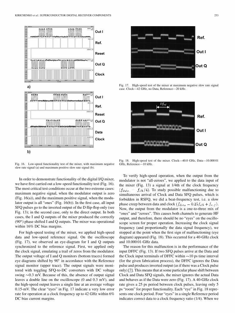
Fig. 16. Low-speed functionality test of the mixer, with maximum negativeslew rate signal (a) and maximum positive slew rate signal (b).
In order to demonstrate functionality of the digital I/Q mixer,we have first carried out a low-speed functionality test (Fig. 16).The most critical test conditions occur at the two extreme cases:maximum negative signal, when the modulator output is zero(Fig. 16(a)), and the maximum positive signal, when the modu-lator output is all “ones” (Fig. 16(b)). In the first case, all inputSFQ pulses go to the inverted output of the D flip-flop only (seeFig. 13); in the second case, only to the direct output. In bothcases, the I and Q outputs of the mixer produced the correctly(90 ) phase shifted I and Q outputs. The mixer was operationalwithin 16% DC bias margins.
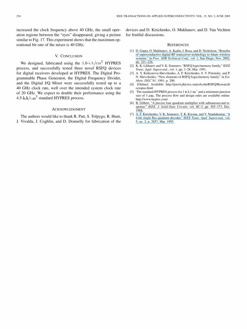
For high-speed testing of the mixer, we applied high-speeddata and low-speed reference signal. On the oscilloscope(Fig. 17), we observed an eye-diagram for I and Q outputssynchronized to the reference signal. First, we applied onlythe clock signal, emulating a trail of zeros from the modulator.The output voltage of I and Q monitors (bottom traces) formedeye diagrams shifted by 90 in accordance with the Referencesignal monitor (upper trace). The output signals were moni-tored with toggling SFQ-to-DC converters with DC voltageswing 0.3 mV. Because of this, the absence of output signalleaves a double line on the oscilloscope (0 and 0.3 mV), andthe high-speed output leaves a single line at an average voltage0.15-mV. The clear “eyes” in Fig. 17 indicate a very low errorrate for operation at a clock frequency up to 42 GHz within 6%DC bias current margins.
Fig. 17. High-speed test of the mixer at maximum negative slew rate signalcase. Clock—42 GHz, no Data, Reference—20 kHz.
Fig. 18. High-speed test of the mixer. Clock—40.0 GHz, Data—10.000 01GHz, Reference—10 kHz.
To verify high-speed operation, when the output from themodulator is not “all-zeroes”, we applied to the data input ofthe mixer (Fig. 13) a signal at 1/4th of the clock frequency
. To study possible malfunctioning due tosimultaneous arrival of Clock and Data SFQ pulses, which isforbidden in RSFQ, we did a beat-frequency test, i.e. a slowphase creep between data and clock .Now, the output from the modulator is a one-to-three mix of“ones” and “zeroes”. This causes both channels to generate HFoutput, and therefore, there should be no “eyes” on the oscillo-scope screen for proper operation. Increasing the clock signalfrequency (and proportionally the data signal frequency), westopped at the point when the first sign of malfunctioning (eyediagram) appeared (Fig. 18). This occurred for a 40-GHz clockand 10.000 01-GHz data.
The reason for this malfunction is in the performance of theinput DFFC (Fig. 13). If two SFQ pulses arrive at the Data andthe Clock input terminals of DFFC within 10 ps time interval(for the given fabrication process), the DFFC ignores the Datapulse and produces inverted output (as if there was a Clock pulseonly) [7]. This means that at some particular phase shift betweenClock and Data SFQ signals, the mixer ignores the actual Dataand behaves as if the Data were zero (Fig. 17). A 40-GHz clockrate gives a 25 ps period between clock pulses, leaving only 5ps “room” for proper functionality. Each “eye” in Fig. 18 repre-sents one clock period. Four “eyes” in a single Reference periodindicates correct data to a clock frequency ratio (1/4). When we
254 IEEE TRANSACTIONS ON APPLIED SUPERCONDUCTIVITY, VOL. 15, NO. 2, JUNE 2005
increased the clock frequency above 40 GHz, the small oper-ation regions between the “eyes” disappeared, giving a picturesimilar to Fig. 17. This experiment shows that the maximum op-erational bit rate of the mixer is 40 GHz.
V. CONCLUSION
We designed, fabricated using the 1.0- HYPRESprocess, and successfully tested three novel RSFQ devicesfor digital receivers developed at HYPRES. The Digital Pro-grammable Phase Generator, the Digital Frequency Divider,and the Digital I/Q Mixer were successfully tested up to a40 GHz clock rate, well over the intended system clock rateof 20 GHz. We expect to double their performance using the4.5- standard HYPRES process.
ACKNOWLEDGMENT
The authors would like to thank R. Patt, S. Tolpygo, R. Hunt,J. Vivalda, J. Coghlin, and D. Donnelly for fabrication of the
devices and D. Kirichenko, O. Mukhanov, and D. Van Vechtenfor fruitful discussions.
REFERENCES
[1] D. Gupta, O. Mukhanov, A. Kadin, J. Rosa, and D. Nicholson, “Benefitsof superconductive digital-RF transceiver technology to future wirelesssystems,” in Proc. SDR Technical Conf., vol. 1, San Diego, Nov. 2002,pp. 221–226.
[2] K. K. Likharev and V. K. Semenov, “RSFQ logic/memory family,” IEEETrans. Appl. Supercond., vol. 1, pp. 3–28, Mar. 1991.
[3] A. Y. Kidiyarova-Shevchenko, A. F. Kirichenko, S. V. Polonsky, and P.N. Shevchenko, “New elements of RSFQ logic/memory family,” in Ext.Abstr. ISEC’91, 1991, p. 200.
[4] [Online]. Available: http://pavel.physics.sunysb.edu/RSFQ/Research/octopus.html
[5] The standard HYPRES process for 1 kA=cm and a minimum junctionsize of 3 �m. The process flow and design rules are available online:http://www.hypres.com/.
[6] B. Gilbert, “A precise four quadrant multiplier with subnanosecond re-sponse,” IEEE. J. Solid-State Circuits, vol. SC-3, pp. 365–373, Dec.1968.
[7] A. F. Kirichenko, V. K. Semenov, Y. K. Kwong, and V. Nandakumar, “A4-bit single flux quantum decoder,” IEEE Trans. Appl. Supercond., vol.5, no. 2, p. 2857, Mar. 1995.


